1
TONE GRABBER 2
DTMF DECODER KIT
Ramsey Electronics Model No.
TG2
Ever wonder what numbers were being dialed on the phone or
radio? Do you need to see what DTMF codes have been used
during the day on the local repeater? Well, this is the kit for you!
Using the power of a microprocessor this unit can record over
600 numbers, and store them in FLASH memory even after
power is removed!
•
Full microprocessor control for simple, but comprehensive features.
•
640 memory locations - FLASH memory holds data for years!
•
Automatically places dashes between sets of numbers for easy
reading of codes!
•
Eight LED displays; see any 8 digits at any time.
•
Able to scroll through memory while unit is operating to see all
memory locations.
•
Decodes all sixteen DTMF codes!
•
Built-in RJ-11 jack for easy interfacing with your phone line as well
as a highly sensitive audio input for custom monitoring!
•
Built-in 1 to 60 digit Data Latch for custom controller applications!
•
Accepts a wide range of supply voltages between 8-15VDC.
TG2 • 1
RAMSEY TRANSMITTER KITS
· FM100B Professional FM Stereo Transmitter
· FM25B Synthesized Stereo FM Transmitter
· MR6 Model Rocket Tracking Transmitter
·TV6 Television Transmitter
RAMSEY RECEIVER KITS
· FR1 FM Broadcast Receiver
· AR1 Aircraft Band Receiver
· SR2 Shortwave Receiver
· SC1 Shortwave Converter
RAMSEY HOBBY KITS
· SG7 Personal Speed Radar
· SS70A Speech Scrambler
· WCT20 Cable Wizard Cable Tracer
· AVS10 Automatic Sequential Video
Switcher
· BS1 “Bullshooter” Digital Voice Storage Unit
· ECG1 Electrocardiogram Heart Monitor
· LABC1 Lead Acid Battery Charger
· LC1 Inductance-Capacitance Meter
RAMSEY AMATEUR RADIO KITS
· DDF1 Doppler Direction Finder
· HR Series HF All Mode Receivers
· QRP Series HF CW Transmitters
· CW7 CW Keyer
· CPO3 Code Practice Oscillator
· QRP Power Amplifiers
RAMSEY MINI-KITS
Many other kits are available for hobby, school, Scouts and just plain FUN. New
kits are always under development. Write or call for our free Ramsey catalog.
TG2 KIT INSTRUCTION MANUAL
Ramsey Electronics publication No. MTG2 Rev 1.1
First printing: February 2002
COPYRIGHT 2002 by Ramsey Electronics, Inc. 590 Fishers Station Drive, Victor, New York
14564. All rights reserved. No portion of this publication may be copied or duplicated without the
written permission of Ramsey Electronics, Inc. Printed in the United States of America.
TG2 • 2
Ramsey Publication No. MTG2
Price $5.00
KIT ASSEMBLY
AND INSTRUCTION MANUAL FOR
TONE GRABBER 2
DTMF DECODER KIT
TABLE OF CONTENTS
Introduction ................................. 4
Circuit Description....................... 4
Parts Layout Diagram ................. 6
Schematic Diagram .................... 7
Parts List .................................... 8
Assembly Instructions ................. 10
Custom Case .............................. 17
Initial Testing .............................. 18
Troubleshooting Guide ............... 19
Using your TG2 .......................... 20
Specifications ............................. 22
Warranty ..................................... 23
RAMSEY ELECTRONICS, INC.
590 Fishers Station Drive
Victor, New York 14564
Phone (585) 924-4560
Fax (585) 924-4555
www.ramseykits.com
TG2 • 3
INTRODUCTION
The Ramsey TG2 is a dual tone multi-frequency (DTMF) decoder with data
retention, 8 character display, and a trigger output enabling the user to activate
an external device when a user selected data match occurs. It decodes all
sixteen DTMF characters and stores them in non-volatile FLASH memory. It
automatically places a dash between incoming codes that have a 3 second
spacing between them to make viewing the data at a later time easier to
understand. To ensure data security, the FLASH memory micro-controller can
store saved codes with the power off for more than 10 years!
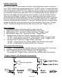
CIRCUIT DESCRIPTION
Take a look at the TG2's Schematic Diagram as we walk through the circuit
description. As you can see there is not much to the Tone Grabber componentwise; most of the work is done internally by the IC's.
The DTMF audio input circuitry has been split into two sections to make
interfacing with the TG2 easier. The ‘Audio In’ (J4) RCA jack accepts line-level
input from almost any audio source and presents it to the DTMF decoder IC.
Pretty simple. The ‘Phone Line Monitor In’ (J3) RJ-11 jack allows you to quickly
hook the TG2 directly to any phone line and continually monitor and ‘grab’ any
DTMF data on the line (keep in mind it does not display digital caller-ID data)!
The audio sniffer formed by C14, C15, R8, R9, and R10 will not capture the line
so it does not interfere with the normal use of your phones. It quietly feeds any
DTMF audio tones to the decoder IC for processing. Protection diodes D2 and
D3 limit the incoming signal to +- 0.7 V so that potentially damaging voltages
like the 90 Vp-p ‘Ring’ signal does not blow-up your decoder IC!
The real heart of the circuit is U3, the tone decoder IC. This chip has the task of
decoding the input tone data from the phone line, or other audio source, and
presenting it in a 4 bit digital fashion to the micro-controller. Internally, this chip
has a set of counters that latch different outputs depending on the tones. The
internal counters are referenced to a television color-burst crystal operating at
3.579 MHz. Some of this reference frequency signal is taken from pin 7 of U3
and is also used to operate the timing control for U1, the micro-controller.
U1 is the preprogrammed 68HC908JK1 micro-controller. This IC contains the
developed code required to take the DTMF tone data from U3 and process it
while updating the displays, reading and writing the data into FLASH memory,
and driving the external ‘Trigger Output’ (J2, more on this in a moment). It also
continually monitors the front panel arrow buttons and takes action accordingly
when the user requests to scan through the stored data or clear the memory.
The previously mentioned external ‘Trigger Output’ on J2 is an Open Collector
transistor driver formed by R7, Q1, and protection diode D4. The microTG2 • 4
controller switches Q1 ‘On’ or ‘Off’ providing the user with a closure to ground
that can be used to drive an external device such as an event counter, further
logic controllers, or even a relay circuit that sets off an alarm (let your
imagination run wild)! Whenever the TG2 grabs a DTMF tone, it compares that
data to the very first code in memory; this is your Trigger Code. The Trigger
Code may be any 1 to 60 digit combination of the 16 different valid DTMF
characters. This means you can look for a particular string, or series, of data
tones that may be embedded within a larger string of data and the TG2 will alert
you by activating Q1 whenever there is a match.
To tell the micro-controller how and when to turn on Q1, jumper blocks J5 and
J6 are set by the user. J5 (Series Mode) handles the ‘when’ aspect of Q1’s
operation. By setting the jumper block for ‘exact match’ (J5 jumper Off) or
‘contains match’ (J5 jumper On), the micro-controller will compare the incoming
DTMF data to that of the very first entry to see if the sequential series matches
up. An ‘exact match’ means that the DTMF entries were exactly the same with
no other digits preceding or following the series (note: there is a 3 second delay
before the Trigger activates to ensure no other data has come in). This is useful
for precise code applications to switch a device on or off. The ‘contains match’
setting means that the proper series was present within a string of received
data. This setting can be used to look for a specific series embedded within a
long entry of data; like looking for the last 7 digits of a restricted phone number!
The J6 (Trigger Mode) jumper determines ‘how’ Q1 will function when a series
match does occur as specified by the user. By setting the jumper block for
‘pulse mode’ (J6 jumper Off), Q1 will turn on and provide a closure to ground
(40VDC @ 2000 mA max) for 1 second before turning off. In ‘toggle mode’ (J6
jumper On), Q1 will alternately toggle on and off each time a series match is
received.
To this point, the only chip we haven’t talked about is U2, a serially loaded
seven segment display driver. This chip can be fully configured by software to
cover things including brightness, testing of the display, low power mode, and
different decode modes for custom characters! It is a really versatile IC and
makes driving the displays much easier for the micro-controller.
VR1 and the surrounding parts C3, C4 and the polarity protection diode D1
form a simple voltage regulator to supply a steady 5 VDC to the ICs on the
board. By using this scheme, we can operate the unit with a wide range of input
supply voltages anywhere from 8 to 15 Volts DC (positive tip on J1).
TG2 • 5
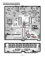
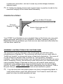
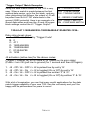
TG2 PARTS LAYOUT DIAGRAM
TG2 • 6
TG2 • 7
PARTS SUPPLIED WITH YOUR TG2 KIT
Capacitors
2 22 pF disc capacitor (marked 22 or 221) [C7,8]
1 470 pF disc capacitor (marked 470 or 471) [C1]
7 .01 µF disc capacitor (marked .01 or 103 or 10 nF) [C2,5,6,9,13,14,15]
3 .1 µF disc capacitor (marked .1 or 104 or 100 nF) [C10,11,12]
1 10 µF electrolytic capacitor [C4]
1 100 µF electrolytic capacitors [C3]
Resistors and Potentiometers
1 1K ohms (brown-black-red) [R3]
9 10K ohms (brown-black-orange) [R1,2,5,7,8,9,10,12,13]
1 47K ohms (yellow-violet-orange) [R11]
1 100K ohms (brown-black-yellow) [R4]
1 330K ohms (orange-orange-yellow) [R6]
Semiconductors and Integrated Circuits
1 1N4000 series diode (black with white band) [D1]
-Note that 1N4002-1N4007 diodes may used.
3 1N4148 diodes (small glass diode) [D2,3,4]
1 2N3904 transistor (three leads TO-92 package marked 3904) [Q1]
1 78L05 +5 volt voltage regulator [VR1]
1 HT9170B DTMF decoder IC (18 pin DIP) [U3]
1 MAX7219 eight digit display driver (24 pin DIP) [U2]
1 68HC908JK1 pre-programmed micro-controller (20 pin DIP) [U1]
(marked with a sticker labeled TG2)
Miscellaneous Components
8 Seven Segment LED displays [DS1,2,3,4,5,6,7,8]
1 3.579 MHz crystal (Marked 3.579 or 3.579545) [X1]
1 2.1 mm DC power jack [J1]
1 3.5 mm mono jack (3 leads) [J2]
1 RJ11 modular phone jack (PCB mount) [J3]
1 RCA jack (PCB mount) [J4]
2 Two pin jumper and jumper block [J5,6]
1 20 pin socket for U1
2 SPST, miniature push button switches (PCB mount) [S1,2]
1 Heatsink, 3/4” x 3/4” layout [HS1]
1 #4-40 Kep nut (HDWE52)
1 #4-40 3/8” screw (HDWE10)
4” #24 AWG Red & Black insulated hookup wire
4” length of #20 buss wire
TG2 • 8
RAMSEY "Learn-As-You-Build KIT ASSEMBLY
There are numerous solder connections on the TG2 printed circuit board.
Therefore, PLEASE take us seriously when we say that good soldering is
essential to the proper operation of your Tone Grabber kit!
•
•
•
Use a 25-watt soldering pencil with a clean, sharp tip.
Use only rosin-core solder intended for electronics use.
Use bright lighting; a magnifying lamp or bench-style magnifier may be
helpful.
Do your work in stages, taking breaks to check your work. Carefully brush away
wire cuttings so they don't lodge between solder connections.
We have a two-fold strategy for the order of the following kit assembly steps.
First, we install parts in physical relationship to each other, so there's minimal
chance of inserting wires into wrong holes. Second, whenever possible, we
install in an order that fits our "Learn-As-You Build" Kit building philosophy. This
entails describing the circuit that you are building, instead of just blindly
installing components. We hope that this will not only make assembly of our kits
easier, but help you to understand the circuit you’re constructing.
For each part, our word "Install" always means these steps:
1. Pick the correct component with the proper value to start with.
2. Insert it into the correct PC board location.
3. Orient it correctly, following the PC board drawing and the written
directions for all parts - especially when there's a right way
and a wrong way to solder it in. (Diode bands, electrolytic
capacitor polarity, transistor shapes, dotted or notched ends
of IC's, and so forth.)
4. Solder all connections unless directed otherwise. Use enough heat
and solder flow for clean, shiny, completed connections.
5. Trim or nip the excess component lead wire after soldering.
NOTE: Save some of the longer wire scraps nipped from resistors and
capacitors. These will be used to form wire jumpers (JMP1, etc.) to be soldered
in just like parts during these construction steps.
Enough of that ... let’s get started!
TG2 • 9
TG2 TONE GRABBER KIT ASSEMBLY
Although we know that you are anxious to complete the assembly of your
Tone Grabber kit it is best to follow the step-by-step instructions in this
manual. Try to avoid the urge to jump ahead installing components.
Since you may appreciate some warm-up soldering practice as well as a
chance to put some landmarks on the PC board, we’ll first install some of the
larger mounting components. This will also help us to get acquainted with the
up-down, left-right orientation of the circuit board. Remember that all of the
components will be mounted on the component side of the circuit board and
soldered on the solder side of the circuit board (the side that contains the
printed circuit traces). Have a look at the parts layout diagram to help with
your assembly.
Use the boxes to check off your progress.
Check all received parts against the parts list. The parts list describes the
various markings that may be found on the kit parts. Carefully sort the parts
into small piles, (an empty egg tray does nicely for this purpose) to aid in
finding the correct part at the required time.
Today's IC’s have achieved remarkable performance levels and it is extremely
unlikely that any of your chips will have problems, yet we know that some of
our hobbyists insist on socketing all IC components. The addition of these will
not “void” your warranty, but if a problem arises from a socketed component
you will be required to pay the additional technician fee for labor in the repair
of your kit, if necessary.
Now we will install the input and output connectors of the circuit. We use
several printed circuit (PC) type jacks to accomplish our interfaces. These
jacks typically have several mounting pins associated with each connector.
Notice on the schematic how these connectors use extra contacts as switches
so that when the plug is inserted the contacts will open. That’s how your
transistor radio turns off the speaker when you plug in your headphones!
Proper Component Installation:
TG2 • 10
1. Locate and install the large modular phone jack, J3.
2. Install R9, 10K ohms (brown-black-orange).
3. Install C14, .01µF ceramic capacitor
(marked .01, 103 or 10 nF). Disc
capacitors are not polarized so they can
be installed in either direction. The reason
we call them “disc” caps can be seen by
the package style. The capacitor itself is
two conductive discs separated by a
dielectric compound.
Cathode
Anode
4. Install C15, .01µF ceramic capacitor
(marked .01, 103 or 10 nF).
5. Install R10, 10K ohms (brown-black-orange).
6. Install R8, 10K ohms (brown-black-orange).
7. Install C11, .1µF ceramic capacitor (marked 104 or .1).
8. Install D2, one of the 1N4148 diodes (small glass diode with black
band). The lead closest to the black band is the Cathode end. Make sure it
lines up with the white band shown on the PC board silkscreen and the
Parts Layout Diagram. Be gentle with this fragile part and double check the
orientation before soldering.
9. Install D3, another 1N4148 diode in the same fashion as D2.
10. Install J4, the RCA type audio jack, by the edge of the board.
11. Install R11, 47K ohms (yellow-violet-orange).
12. Install C13, .01µF ceramic capacitor (marked .01, 103 or 10 nF).
13. Install C12, .1µF ceramic capacitor (marked 104 or .1).
You’ve just finished phone line audio monitor through J3 and the line level
audio monitor through J4 input circuitry! Make sure you’re saving those clipped
off leads to use as jumpers later. We’ll need 7 of them!
14. Install U3, the 18 pin DIP tone decoder chip marked HT9170B. Make
absolutely sure it is mounted in the proper direction. The small semi-circle
on the IC represents pin 1 and should be mounted in the same direction as
in the Parts Layout Diagram. Not all ICs in this kit are mounted in the same
direction as this one so keep this in mind with later IC installations.
15. Install R3, 1K ohms (brown-black-red).
16. Install R4, 100K ohms (brown-black-yellow).
17. Install X1, the 3.579 MHz crystal (silver metallic can marked 3.579).
TG2 • 11
Make sure it is flush to the board before soldering.
18 Install C8, 22 pF disc capacitor (marked 22).
19. Install C7, 22 pF disc capacitor (marked 22).
20. Install R6, 330K ohms (orange-orange-yellow).
21. Install C10, .1µF ceramic capacitor (marked 104 or .1).
This concludes the assembly of the entire DTMF decoder section!!! Now let’s
tackle the micro-controller and a few of its peripherals.
22. Install the 20 pin DIP socket for U1, the 68HC909JK1 micro-controller
IC. It doesn’t matter which way the socket is oriented, as long as the chip is
placed in the socket correctly. You can bend two of the corner leads out
slightly to hold the socket in place when you flip the board over to solder it
in. Be sure to solder all 20 pins.
23. Now insert U1, the micro-controller marked with a sticker labeled TG2
into the socket. Orient the notched end as shown on the PC board
silkscreen, toward J4. Before you push it down into the socket check to be
sure that none of the pins are bent under or outside of the socket. When
you’re sure the pins are where they belong, press it down so that it is
seated flat within the socket.
24. Install C1, 470 pF disc capacitor (marked 470 or 471). This capacitor
couples over a bit of the X1 clock signal from U3 to run the micro-controller.
25. Install C2, .01µF ceramic capacitor (marked .01, 103 or 10 nF).
26. Install J6, the two pin ‘Trigger Mode’ jumper. Once it is soldered in you
can place the jumper block on it so that you don’t lose it! Notice the quick
reference silkscreen on the board listing the jumper configuration setups.
27. Install R13, 10K ohms (brown-black-orange).
28. Install J5, the other two pin jumper. This one is for the ‘Series Compare’
user configuration setting.
29. Install R12, 10K ohms (brown-black-orange).
Now for the external trigger circuitry that is controlled by the micro-controller.
30. Install D4, the last 1N4148 diode with the glass body.
31. Install J2, the mono 3.5 mm external ‘Trigger Output’ jack. Proper
positioning of this part will help you later with case-up so be sure it’s where
you want it before soldering.
32. Install Q1, the transistor marked 2N3904. The flat side must be placed
as shown on the PC board. Mount it as close to the board as possible
without forcing it. This component provides you with the Open Collector
TG2 • 12
trigger output.
33. Install R7, 10K ohms (brown-black-orange).
Take those clipped off scrap leads from the components you’ve installed and
let’s put in jumper wires 1 through 7. These act like electronic bridges that
connect circuit traces over the top side of the PC board.
34. Using one of the scrap component leads, install JMP1. Form it into a
staple-like shape and insert it into the holes shown on the silkscreen of the
PC board. Make sure you solder both ends of the wire to ensure proper
operation. See the Parts Layout Diagram for clarification if necessary.
35. In the same fashion as JMP1, install JMP2, 3, 4, 5, 6, and 7.
On to the display driver!
36. Install U2, the 24 pin DIP marked MAX7219. This is the display driver
chip that runs the eight displays on the display board. Be careful soldering
this part as it is easy to forget a pin or solder a pin to a nearby lead. Also
make sure and check its orientation in comparison to the Parts Layout
Diagram before soldering.
37. Install R1, 10K ohms (brown-black-orange).
38. Install C5, .01µF ceramic capacitor (marked .01, 103 or 10 nF). There
is not much to this section but the actual displays are yet to come!
39. Install C6, .01µF ceramic capacitor (marked .01, 103 or 10 nF).
40. Install C9, .01µF ceramic capacitor (marked .01, 103 or 10 nF). Note
that C6 and C9 are actually part of the user switch assembly (S1 and S2).
This was just the best time to put them in!
We’ll finish off the component section of the main board now by building up the
power supply circuitry.
41. Identify and install the power connector J1, the 2.1 mm DC power jack
at the edge of the PC board. Gently slide the leads through the component
side of the circuit board until the connector is mounted flush. Solder all
three connections using enough heat to flow the ground connection
completely.
42. Install D1, the 1N4004 diode (black epoxy body with a white band).
Watch your polarity like you did with D2!
43. Install VR1, the 7805, 3 terminal voltage regulator. Place the heatsink,
HS1, on the circuit board, lining it up with the silkscreen so that the hole in
the heatsink matches the hole in the board. Take the 7805 and place it on
top of the heatsink so that the hole in the regulator lines up with the other
two. This will show you where to bend the leads down so that the part fits in
the PC board holes and lays flat on the heatsink allowing maximum “bleed
TG2 • 13
off” of heat from the part. Once the leads are bent and through the PC
board holes, take the screw and nut and attach the 7805 and the heatsink
to the board. In order for the unit to properly mount in its case, insert the
screw from the bottom side of the PC board and place the holding nut on
the top side. Once the screw is tightened and holding everything in place
solder the three leads of the 7805.
44. Install C3, 100 µF electrolytic capacitor. This part also must be installed
properly to function. In fact, this capacitor has the potential to explode if
installed in reverse polarity! The PC board silkscreen shows the positive
hole and the band on the capacitor shows the negative side. You’ll also
note that the lead closest to the stripe is shorter than the other lead; this
also indicates the negative side.
45. Install C4, 10 µF electrolytic capacitor. Watch that polarity!
46. Locate the Red and Black #24 AWG insulated hookup wire provided in
your kit. Strip both ends of each wire back approximately 1/4" and
"tin" (melt solder on) all four ends to hold the loose strands together.
47. Using the Red wire, install the jumper between the holes marked
JMPA1 and JMPA2.
48. With the Black wire, jumper between the holes marked JMPB1 and
JMPB2. These feed the front panel user switch info to the micro-controller.
Now here comes the fun part, the front panel display board! Take your time on
the next few stages as they can make or break your kit. Don't be in a rush to
get it done, hook it up, and find you misinterpreted a step and cause big
trouble! Play it smart and have patience and your kit will make you proud when
it works the first time!
49. Install DS1, one of the seven segment displays. Pay very close
attention to where the decimal point is! It should be positioned in the lower
right hand corner when installed correctly. Check and double check
orientation before soldering, since desoldering on these fine traces will
absolutely destroy them. Make sure the display is flush to the board before
soldering; you can bend a few leads slightly over to assist in holding it there
while you solder. Use the specialized soldering skills that you learned
earlier in this kit, and make sure that there are no solder bridges between
pins and other traces on the board. Also make sure you still heat the joints
hot enough for a good solid connection.
50. Hope you had an OK time doing the first display; now you get to do it
seven more times! Install DS2 - DS8 using the same technique as before.
Start with DS2 and proceed in order, ending with DS8. This prevents finger
squeezing and much ranting and raving.
51. Install R2, 10K ohms (brown-black-orange). Keep it close to the board!
TG2 • 14
52. Install R5, 10K ohms (brown-black-orange). Keep it close again!
53. Install S1, one of the pushbutton switches. Notice that this part only
fits comfortably in one direction. Mount this switch flush to the board.
54. Install S2 in the same fashion, making sure that it to is flush to the
board.
Whew! That was some work. But we’re almost done. Now is a good time to
recheck all your work up to this point. Carefully inspect the circuit boards for
stray leads or open solder connections, trim and touch up any that need work.
Now here comes some more fun! It's time to join the two boards together.
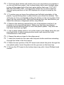
55. Notice the holes in the main board and the display board where SUP1
and SUP2 are located. Using two pieces of stiff buss wire or spare
component leads, install the supports to hold the main board and the
display boards at a 90 degree angle to each other. Note how the display
board is mounted with the solder side toward the main board. Do not
solder the display board ends of the supports until after the finger tabs are
attached in the next step. This will give you a bit more flexibility and make
it easier to position the display at the proper angle.
56. The display board mounts at a right angle to the main board with
solder pads providing both mechanical support and electrical connection
between the two boards. The display board is placed against the main
board so that the solder pads on the display board line up with the solder
pads on the main board. Solder the display board pads flush with the main
board pads. Check to be sure the two boards are perpendicular and not
tilted, then solder all remaining pads. Use enough solder to provide a
good
Support
wire
Display
board
Solder
fillet
TG2 • 15
Main
board
mechanical connection, but don’t cause any solder bridges between
adjacent pads.
57. Solder the display board ends support wires in position to add to the
structural integrity of the entire board assembly.
CONGRATULATIONS !
Top of Main PC board
Front of
Dis play PC Board
Solder f illet betw een PC
boards
Your DTMF Tone Grabber is now complete! Have a final look over your work,
paying particular attention to the orientation of diodes, capacitors, and IC’s.
Remember that any problems you find now can save time and effort after the
unit has been cased up.
ASSEMBLY INSTRUCTIONS FOR CUSTOM CASE
The enclosure is a key element to the overall pride you will have upon
completing your Ramsey kit. The enclosure will show how you were able to
“build from scratch” a commercial piece of high-tech electronics. For some of
us, the enclosure will also hide a number of “not-so-pretty” assembly
mistakes. Once the kit is enclosed, your friends will never know that you were
new to soldering. Finally, the enclosure case will protect your electronics from
many possible causes of damage so that you can receive years worth of
enjoyment using, talking about, and remembering the fun you had building
your kit. In short, TAKE YOUR TIME when assembling the enclosure. This is
the part that you and your friends will look at and admire for years!
1. Lay the front and rear plastic plates over their corresponding labels to
verify which sticker goes with which panel. You’ll want to work with one
panel at a time to avoid possible mix-ups.
TG2 • 16
2. The front panel sticker will need to be cut to size before you position it
on the red front lens panel. Use a sharp hobby knife and a straight edge
to trim off the upper half of the front panel sticker that says “CUT OFF
BELOW DOTTED LINE”. Cut below the dotted line to ensure that the
decimal point positions of the LED displays do not get covered by the
sticker.
3. To make sure you know the up/down and left/right orientation of the
panels, try positioning them in place before you mount the stickers. This
will keep you from accidentally putting the sticker on the wrong side of the
panel you are working with. Remove the panels from the case before you
attach the stickers or alignment will be very difficult.
4. Remove the backing material from one of the stickers and line it up
properly on its pre-punched panel. Make sure that they are aligned
correctly before allowing them to touch the plastic plates. They stick the
first time; line them up right!
5. Use a sharp hobby knife to cut out the holes in the labels along the prepunched holes. A short sawing motion works well around the inner
circumference of the holes.
6. Repeat the above steps for the other panel.
7. Insert the board into the case with the push button switches extending
through the holes in the front panel.
8. Raise the rear portion of the PC board and extend the jacks through the
rear plastic plate. Insert the plate into the grooves on the base tray.
9. Secure the PC board to the bottom base tray with 4 short Phillips head
screws.
TG2 • 17
TG2 INITIAL TESTING:
Now that the assembly of the unit has been completed, we can move on to
testing it! To start with, we are going to need to gather a few items to help us
test the circuitry.
•
A radio, or a DTMF generator, with an RCA audio patch cable (J3).
OR
•
A phone line, with an RJ-11 telephone patch cable, and a phone (J4).
•
A power supply 8-15 VDC @ 500 mA (J1)
(The Ramsey AC125 is ideal 12 VDC @ 500 mA)
1. Verify that all parts are mounted and soldered in the correct places.
Make sure there are no solder bridges or cold solder joints.
2. Connect the audio source with the DTMF tones to J3 or J4 respectively.
3. Carefully plug in the power to your kit (J1) making sure the center pin is
positive. The display will briefly flash all “8”s to test each segment.
[On first time power up the memory should be all dashes except for one test
phone number that has been programmed into memory as the initial Trigger
Code.] If nothing lights on your first power up, quickly unplug the power and
consult the troubleshooting section of the manual. If all of the displays light in
some fashion, then you’re OK for now.
4. Press and hold both buttons at the same time until the display begins to
flash. This is how to clear the regular data memory. To clear the Trigger
Code you’ll need to press a both buttons again; this prevents having to
reenter the Trigger Code ever time the memory is full. Note that this takes
about a second or more to do when operating correctly.
5. Press and hold the left button, and then the right to verify that the
decimal point moves in the proper directions. These buttons scroll the
“window” across the available 640 memory locations.
6. Generate some tones into your Tone Grabber with the decimal point lit
on the right most display. You should see the appropriate numbers and
characters light on the display and scroll to the left.
7. Generate a series of eights to verify that all of the segments of your
displays are operating properly.
If you have made it this far with your kit and have had no problems, you’re all
set to go! If not, consult the troubleshooting guide in the manual to determine
the cause of the problem and how to go about solving it.
TG2 • 18
TROUBLESHOOTING GUIDE
If your TG2 does not work at all, recheck the following:
•
correct orientation of U1, U2 and U3 (see PC board layout diagram)
•
correct polarity of all electrolytic capacitors.
•
correct orientation of diodes D1 through D4
•
all solder connections
•
jumper wires at all JMP locations.
Still having trouble?
While we had hoped that it wouldn’t come to this, if you are still having trouble
with your TG2, here are a few additional suggestions.
PROBLEM: None of the displays light and VR1 regulator gets hot fast.
SOLUTION: You likely have a short across the power supply or you have a
component placed in the incorrect orientation. Check all of your parts to make
sure they correlate with those in the Parts Layout Diagram.
PROBLEM: None of the displays light and VR1 remains cool.
SOLUTION: Using an oscilloscope or a frequency counter to verify that there
is a 3.579 MHz signal on pin 7 of U3 and pin 3 of U1. It should be
approximately 0.5 Vp-p or greater. If you cannot check the oscillator, verify
that 5 Volts DC is present on the IC power pins (U1:5, U2:19, and U3:18). If
not, check VR1 for 5 VDC output with at least 8 VDC input from your power
supply.
PROBLEM: Some displays and segments light but others do not.
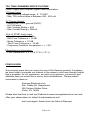
SOLUTION:
are only
two possibilities for this problem. First check with
Display
Conversions:
J6 - TriggerThere
Mode
a OFF
magnifier
to verify
- Pulse
Modethat there are no shorts or cold solder joints on the display
board
displays. Also check the interface between the two boards to
ON -behind
Togglethe
Mode
8 correctly. Second, you may have a
make sure everything0has been done
faulty
display.
Since
this
is
very
unlikely,
check all of your solder joints again to
9
J5 - Series Compare
1
make
sure
they
are
OK.
If
everything
is
fine,
then see the warranty section of
OFF - Exact Match 2
A
the
manual.
ON - Contains Match
3
B
PROBLEM: Everything
no tones can be detected.
4 is OK, but C
SOLUTION: Check around U3 and J3 and J4 for bad solder joints. Also check
5 to the unit.D
your audio connections
6
#
Have another set of eyes look over your work. Here at the shop we have often
run into a “stone wall”7of a problem*only to have a fellow technician see our
obvious error. It is sometimes very difficult to see your own mistakes.
TG2 • 19
USING YOUR TG2
Now we’re ready for the moment of truth, the initial power up and running of
your TG2! Connect your power supply (8 to 15 VDC) to the J1 power jack and
your audio source with the DTMF codes you wish to detect, i.e. the phone line
(J3) or radio line out (J4). You can leave it running all day and come back later
to review the codes that were used. The unit automatically inserts dashes so
that you can easily tell one code set from another (if you fill all 640 memory
slots the unit will begin to flash). The front panel arrow buttons allow you to
scroll through the stored data and view up to 8 characters at a time; note that
the decimal point marks the position of the next open data field. To clear the
memory, press both arrow keys for 1 second. This will remove all stored data
except for the first entry (the series up to the first dash), this is your “Trigger
Code”. Double clearing the memory will remove the old “Trigger Code”.
User Controls:
1. Left arrow button scrolls through the data to the left.
2. Right arrow button scrolls through the data to the right.
3. Both buttons (for 1 second) to clear all but the “Trigger Code”.
4. Both buttons again (for 1 second) to clear “Trigger Code”.
5. Jumper block J5 sets the “Series Compare” operation.
- J5 OFF - Data series must be an “Exact Match” of the “Trigger Code”.
- J5 ON - Data series must only “Contain Match” of the “Trigger Code”.
6. Jumper block J6 sets the “Trigger Mode” operation.
- J6 OFF - Toggle output On (active GND) and Off with each match.
- J6 ON - Pulse output On (active GND) for 1 second.
Automated Data Handling:
1. A dash “-” is automatically inserted between data stings after 3 seconds.
2. A decimal point shows the location of the next data entry.
3. The 1st data series up to the 1st dash is the “Trigger Code” .
-To change the “Trigger Code” you must first double clear the memory.
“Trigger Output” (J2) External Connections:
Buzzer speaker
TG2 • 20
“Trigger Output” Match Examples:
Using the data match feature of the TG2 is very
easy. When a match is made between the first
entered data series, up to the first dash, and any
other data string that follows, the output of J2 will
be pulled from its Hi-Z ‘Off’ state down to the
ground (GND) potential. Here is an example of a
stored data series and how the J5 and J6 jumper
block settings control the J2 “Trigger Output”:
J6 - TRIGGER CODE
OFF - PULSE MODE
ON - TOGGLE MODE
J5 - SERIES COMPARE
OFF - EXACT MATCH
ON - CONTAINS MATCH
1234-0-411-18004462295-15859244560-0123456789-1234-.
Data string break down:
A. 1234 <<< first entry “Trigger Code”
B. 0
C. 411
D. 18004462295
E. 15859244560
F. 0123456789
G. 1234
J2 activation (active low) for the above codes:
(Toggle = change On or Off state of J2 based on its prior state)
(Pulse = turn On (pull low to ground) for 1 second and then Off again)
1.
2.
3.
4.
J5 - Off / J6 - OFF => J2 is pulsed low by entry ‘G’.
J5 - Off / J6 - On => J2 is toggled (On or Off) by entry ‘G’.
J5 - On / J6 - OFF => J2 is pulsed low entries ‘F’ & ‘G’.
J5 - On / J6 - On => J2 is toggled (On or Off) by entries ‘F’ & ‘G’.
With a bit of imagination, you can find many useful applications for the data
match trigger capability of your new TG2. Use the unit wisely and you’ll be
happy with its performance for years to come!
TG2 • 21
TG2 TONE GRABBER SPECIFICATIONS
Power Supply and External Signal Level Information:
J1 Power Input
- Input working voltage range: 8 - 15 VDC
- Max TG2 current draw is between 400 - 450 mA.
J2 “Trigger Output”
- Active Low - On = ground (0VDC)
- Hi-Z Off state
- Max Voltage Rating = 40V
- Max Current Rating = 200mA
J3 & J4 DTMF Audio Input
- Signal Level = -29 to 1 dBm
- Dial Tone Tolerance = 10 dB
- Noise Tolerance = -12 dB
- Third Tone Tolerance = -16 dB
- Frequency Deviation Acceptance = +- 1.5%
Miscellaneous Information:
- PCB Dimensions: 4.5” L x 4.0” W x 1.2” H
CONCLUSION
We sincerely hope that you enjoy the use of this Ramsey product. As always,
we have tried to compose our manual in the easiest, most user-friendly format
that is possible. As our customers, we value your opinions, comments, and
additions that you would like to see in future publications. Please submit
comments or ideas to:
Ramsey Electronics Inc.
Attn. Hobby Kit Department
590 Fishers Station Drive
Victor, NY 14564
Please also feel free to visit our Website at www.ramseyelectronics.com and
offer your observations to other kit enthusiasts as well.
And once again, thanks from the folks at Ramsey!
TG2 • 22
The Ramsey Kit Warranty
Please read carefully BEFORE calling or writing in about your kit. Most problems can be
solved without contacting the factory.
Notice that this is not a "fine print" warranty. We want you to understand your rights and ours too!
All Ramsey kits will work if assembled properly. The very fact that your kit includes this new manual
is your assurance that a team of knowledgeable people have field-tested several "copies" of this kit
straight from the Ramsey Inventory. If you need help, please read through your manual carefully.
All information required to properly build and test your kit is contained within the pages!
1. DEFECTIVE PARTS: It's always easy to blame a part for a problem in your kit, Before you
conclude that a part may be bad, thoroughly check your work. Today's semiconductors and passive
components have reached incredibly high reliability levels, and it’s sad to say that our human
construction skills have not! But on rare occasions a sour component can slip through. All our kit
parts carry the Ramsey Electronics Warranty that they are free from defects for a full ninety (90)
days from the date of purchase. Defective parts will be replaced promptly at our expense. If you
suspect any part to be defective, please mail it to our factory for testing and replacement. Please
send only the defective part(s), not the entire kit. The part(s) MUST be returned to us in suitable
condition for testing. Please be aware that testing can usually determine if the part was truly
defective or damaged by assembly or usage. Don't be afraid of telling us that you 'blew-it', we're all
human and in most cases, replacement parts are very reasonably priced.
2. MISSING PARTS: Before assuming a part value is incorrect, check the parts listing carefully to
see if it is a critical value such as a specific coil or IC, or whether a RANGE of values is suitable
(such as "100 to 500 uF"). Often times, common sense will solve a mysterious missing part
problem. If you're missing five 10K ohm resistors and received five extra 1K resistors, you can
pretty much be assured that the '1K ohm' resistors are actually the 'missing' 10 K parts ("Hum-m-m,
I guess the 'red' band really does look orange!") Ramsey Electronics project kits are packed with
pride in the USA. If you believe we packed an incorrect part or omitted a part clearly indicated in
your assembly manual as supplied with the basic kit by Ramsey, please write or call us with
information on the part you need and proof of kit purchase.
3. FACTORY REPAIR OF ASSEMBLED KITS:
To qualify for Ramsey Electronics factory repair, kits MUST:
1. NOT be assembled with acid core solder or flux.
2. NOT be modified in any manner.
3. BE returned in fully-assembled form, not partially assembled.
4. BE accompanied by the proper repair fee. No repair will be undertaken until we have received
the MINIMUM repair fee (1/2 hour labor) of $25.00, or authorization to charge it to your
credit card account.
5. INCLUDE a description of the problem and legible return address. DO NOT send a separate
letter; include all correspondence with the unit. Please do not include your own hardware
such as non-Ramsey cabinets, knobs, cables, external battery packs and the like. Ramsey
Electronics, Inc., reserves the right to refuse repair on ANY item in which we find excessive
problems or damage due to construction methods. To assist customers in such situations,
Ramsey Electronics, Inc., reserves the right to solve their needs on a case-by-case basis.
The repair is $50.00 per hour, regardless of the cost of the kit. Please understand that our
technicians are not volunteers and that set-up, testing, diagnosis, repair and repacking and
paperwork can take nearly an hour of paid employee time on even a simple kit. Of course, if we find
that a part was defective in manufacture, there will be no charge to repair your kit (But please
realize that our technicians know the difference between a defective part and parts burned out or
damaged through improper use or assembly).
4. REFUNDS: You are given ten (10) days to examine our products. If you are not satisfied, you
may return your unassembled kit with all the parts and instructions and proof of purchase to the
factory for a full refund. The return package should be packed securely. Insurance is
recommended. Please do not cause needless delays, read all information carefully.
TG2 • 23
TG2 TONE GRABBER KIT
Quick Reference Page Guide
Introduction ...................................... 4
Circuit Description ............................ 4
Parts Layout Diagram ...................... 6
Schematic Diagram .......................... 7
Parts List .......................................... 8
Assembly Instructions ...................... 10
Troubleshooting Guide..................... 19
Using your TG2 ................................ 20
Specifications ................................... 22
Warranty .......................................... 23
REQUIRED TOOLS
• Soldering Iron
Ramsey WLC-100,
• Thin Rosin Core Solder
Ramsey RTS12
• Needle Nose Pliers
Ramsey RTS05
• Small Diagonal Cutters
Ramsey RTS04
<OR> Complete Soldering Tool Set RS64-2801
ADDITIONAL SUGGESTED ITEMS
• Optivisor Magnifier Headband
• Holder for PC Board/Parts
• Desoldering Braid
Ramsey OPMAG
Ramsey RTS13,
Ramsey RTS08
Price: $5.00
Ramsey Publication No. MTG2
Assembly and Instruction manual for:
RAMSEY MODEL NO. TG2
TOTAL SOLDER POINTS
270
ESTIMATED ASSEMBLY
TIME
Beginner ........... 3.0 hrs
Intermediate .........2.5 hrs
Advanced .............1.5 hrs
RAMSEY ELECTRONICS, INC.
590 Fishers Station Drive
Victor, New York 14564
Phone (585) 924-4560
Fax (585) 924-4555
www.ramseykits.com
TG2 • 24