1
SL 486YB
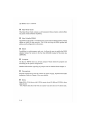
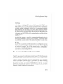
INTRODUCTION!
This manual has been designed for several purposes. If the SL 486VE is
already set up in a functioning system, it will be helpful to reviewthe manual
to become familiar with the features of the board and where things are. This
will be helpful in the unlikely event there is a problem with the system.
For those who want to alter the board's configuration or upgrade it, the
manual will serve as a guide to both procedures and specifications. While
the necessary information is included in the manual, we recommend that
unless you feel confident of your ability to do the work, it would be best to
have your dealer or a local service shop do it. Before making alterations to
the system, check to see that doing so will not violate the system warranty. If
it does, have the work done by an authorized dealer.
The "chip set"consists of six chips; SiS85C411/420/431/405/406, which incorporate most of the logic required for a low-cost, highly integrated IBM PC
AT-compatible computer.
IMPORTANT:
The chip set requires correct configuration information; otherwise a malfunction may result.
CAUTION:
Static electricity can cause serious damage to
integrated circuit chips. To avoid building up a
static electric charge on your body, touch a
grounded object before touching the chips and
at frequent intervals as you handle the chips. If
chips are handed from one person to another,
the two should touch hands first, then pass the
chips.
i
Information presented in this publication has been carefully checked for
reliability; however, no responsibility is assumed for inaccuracies. The
information contained in this document is subject to change without notice.
Contact your dealer for warranty details.
Trademarks
AMI Modular BIOS is a trademark of American Megatrends Inc.
IBM, PC, AT, and PS/2 are registered trademarks of
International Business Machines Corporation.
SiS is a registered trademark of Silicon Integrated Systems Corp.
ii
•
CONTENTS
CHAPTER 1
INTRODUCTION
1.1
1.2
General Specifications and Features
Major Components
1-1
1-2
CHAPTER 2
MEMORY CONFIGURATION
2.1 System Memory
2.1.1 DRAM Module Insertion
2.1.2 DRAM Module Removal
2.2 Cache Memory Subsystem
2-1
2-2
2-3
2-3
CHAPTER 3
JUMPERS SETTING AND CONNECTORS
3.1
3.2
Jumper Settings
Connectors
3-1
3-3
APTER 4
BUILT-IN BIOS SETUP PROGRAM
4.1 Setup Summary
4.2 BIOS Setup
4.2.1 When Should You Run Setup ?
4.2.2 How to Recall the Setup Program ?
4-1
4-2
4-2
4-2
1/CONTENTS
•
CONTENTS
4.2.3 Running the SETUP Program
4.3 Running the Standard CMOS Setup
4.4 Running the Advanced CMOS Setup
4.5 Running the Advanced CHIPSet Setup
4.6 Using the Change Password Setup
4.7 BIOS Errors and Messages
4.7.1 Fatal Errors Through Beeps
4.7.2 Non-Fatal Errors Through Beeps
4.7.3 Fatal Errors Shown in Display
4.7.4 Non-Fatal Errors in Display
4.7.5 Errors With Setup Option
4.7.6 Errors Without Setup Option
4-4
4-5
4-7
4-9
4-12
4-13
5-13
5-14
5-14
5-14
5-15
5-15
CHAPTER 5
EISA Configuration Utility
5.1 EISA Specification
5.1.1 EISA AS A Differences
5.1.2 EISA Bus Specification
5.1.3 EISA Configuration Utility Features
5.2 Configuring Your Computer for the First Time
5.3 Installing the ECU
5.4 Running the EISA Configuration Utility
5.4.1 Main Menu
5.4.2 Using Help
5.5 About EISA Configuration
5.6 Add and Remove Boards
5.6.1 Change Configuration Settings
5.6.2 View Switch/Jumper Settings
5.7 Define ISA Board
5.8 Check CFG File
5.9 Write Ext CMOS
2/CONTENTS
5-1
5-1
5-2
5-2
5-3
5-4
5-5
5-6
5-7
5-8
5-10
5-11
5-12
5-12
5-18
5-14
•
CONTENTS
5.10 Board ID Map
5-14
5.11 Other Main Menu Options
5-14
APPENDIX A
HARD DISK TYPES
APPENDIX В
SETTING THE SYSTEM SPEED
3/CONTENTS
Introduction
Chapter 1
Introduction
This chapter will cover the general specifications and features of the SL 486VE.
1.1
General Specifications and Features
The SL 486VE mainboard is based on the powerful 80486 microprocessor and
incorporates advanced computer technology to meet the requirements of the
next generation of operating systems and applications. Yet, it retains full
compatibility with the original IBM XT and AT and uses existing PC software
and hardware.
•
Co-processor:
Support primary CPU with 80486SX for 25/ 33 MHz,
80486DX for 25/ 33/ 50 MHz or
80486DX2 for 50/ 66 MHz
Support CPU upgrade socket with OverDrive™ CPU.
All the above are packed in PGA package.
о
Memory
n Cache:
Write-back/ write-through selectable direct mapped cache controller.
Support 64KB/ 128KB/256KB Cache memory size.
Two programmable Non-Cacheable regions.
a Memory:
Support 486 burst and EISA burst modes to local memory access.
Bank Interleaved Fast Page Mode DRAM access.
Support 256KB/ 1MB/ 4MB/ 16MB 30-pin SIMM module from 1MB
to 128MB main memory.
.
Support AMI 64 KB BIOS.
.
CHIPSet: SIS85C411/ С420/ С431/ С405/ C406 EISA CHIPSet.
1-1
SL 486VE User's
•
Manual
Slots:
П 8 EISA slots with 6 EISA-master slots (S1-S6) and 2 EISA slave slots
(S7, S8).
n Two VESA slots (S9, S10) with one master/ one slave slot or two slave
slots.
•
Form Factor: Baby AT size, 6 layers PCB SMD design.
1.2
Major Components
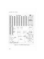
The SL 486VE mainboard is composed of many integrated circuits, chips,
jumpers and connectors. (Please refer to Figure 3.1)
The major components and their basic features and functions are outlined as
below:
•
8 0 4 8 6 CPU (Central Processing Unit)
The central processing unit is the brain of a computer system that interprets
and executes instructions, such as performing calculations, routing information, and temporarily storing data. In personal computers, the CPU is a highly
integrated chip called the microprocessor.
11 SiS/EISA 4 8 6 Chipset
The SiS85C405, 85C406 , 85 C411, 85C420, and 85C431 chipset supports
486-based EISA system. Such chipset is achieved through a very high level of
function integration, system partition and is proven to be a highe performance,
compact and cost-effective product. This EISA chipset consists of the following:
П SiS85C405 (Address Buffer)
The Address Buffer is a buffer interfacing between EISA LA and SA
address bus. It also contains EISA bus refresh counter to generate address
during refresh cycle.
n SiS85C406 (Highly Integrated System Peripheral)
The Highly Integrated System Perpheral integrates all the necessary
peripheral control logic used in eisa specific applications, the SiS85C406
4-2
Introduction
consists of: an arbitration scheme that allows efficient bus sharing among
multiple EISA masters, the host CPU, Refresh, and DMA devices; a
seven-channel programmable DMA Controller, a 16 level programmable interrupt controller which provides level or edge triggered interrupt
capability on a channel-by-chaneel basis; non-maskable interrupt logic
for multiple NMI control and generatin; five counters/timers which
provide a system timer interrupt, DRAM refresh requests, a fail safe
timer, a speaker tone output, and a periodic CPU speed control. Besides,
SiS85C406 also integrates the imperative glue logic in EISA system to
further minimize the number of board components.
П SiS85C411 (System/Cache/DRAM Controller)
The System/Cache/DRAM Controller provides powerful cache, DRAM
and CPU interfaces utilizing the integration of faster and configurable
memory functions and most efficient cache systems. Its memory logic
circuit can respond to the CPU and EISA burst cycle allowign faster
transfer operations. With its bank (or double-word) memory interleaving, systems at full speed can attain the utmost memory speed.
a SiS85C420 (EISA Bus Controller)
The EISA Bus Controller is a generic EISA Bus Controller which
contains all the necessary logic to control EISA bus cycles in the system
level design. The SiS85C420 provides the state machines that interfaces
to the host, EISA, and ISA buses, and is loosely coupled with SiS85C411
to support 8-, 16-, and 32-bit masters and slaves. SiS85C420, combining
with SiS85C406, creates a full feature of EISA system board.
n SiS85C431 (EISA Data Buffer)
The EISA Data Buffer is a general data path chip that provides all the
data routing and swapping between the host data bus, memory data bus,
and EISA data bus. It also contains parity genertion and detection logic.
•
Real-Time Clock
The Real-Time Clock contains a self-contained lithium battery which offers
ten years of data retention capability.
1-3
SL 486VE User's
•
Manual
Real-Time Clock
The Real-Time Clock contains a self-contained lithium battery which offers
ten years of data retention capability.
•
Non-Volatile SRAM
The NVM employs 4K x 4 of SRAM and a self-contained lithium battery which
offers ten years of data retention. The NVM can keep the EISA system and
add-on card configuration information.
A
BIOS
In addition to reducing space and cost, it allows the user to enable the BIOS
shadow feature for access to the fast chip (DRAM) instead of the slow one
(EPROM).
•
Jumpers
On the SL 486VE there are several jumpers which should be properly set
according to the system configuration.
Detailed information regarding all jumpers can be obtained from Chapter 3.
•
Connectors
Several connectors are used to connect the power supply, keyboard and LED
indicators. Refer to Chapter 3 for more details.
•
Slots
Eight EISA 32-bit slots with 6 EISA-master slots (S1-S6) and 2 EISA- slave
slots (S1,S2
Two VESA slots (S9, S10) with one master/ one slave slot or two slave slots.
4-4
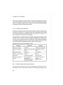
Memory
Configuration
Chapter 2
Memory Configuration
In this chapter, the SL 486VE DRAM configurations are discussed, followed
by instructions for DRAM module installation and removal. Users are recommended to read through this chapter before installing or removing memory.
2.1
System Memory
The SL 486VE provides tremendous flexibility to support a number of different
on-board DRAM configurations. The on-board DRAM is installed with SIMM
(Single-In-Line Memory Module). There are two banks of DRAM module
slots seated on the SL 486VE to support up to 128 MB of on-board memory.
The location and layout of all the SIMM banks is illustrated below and shown
in Figure 3.1:
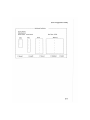
BANK
0
BANK
1
SIMM M EIV О RY
Each bank is composed of four standard 30-pin SIMM sockets. These sockets
take 256KB, 1MB, 4MB, 16MB SIMM.
2-1
SL 486VE User's
Manual
Note that all of the four SIMMs within a bank must be of the same type; you
can not mix 256KB, 1MB, 4MB, or 16MB modules in the same bank.
The SL 486VE board provides 8 sockets for SIMM modules. These 8 sockets
are divided into two banks and each bank can accommodate four SIMM
sockets. Every bank can accept 256KB, 1MB, ,4MB or 16MB SIMM modules,
but all of the four SIMM modules used in the same bank must be the same size.
This ability for mixing assorted SIMM modules on the two banks allows the
system to be shipped with minimal memory and upgrade without sacrificing
the memory already on board.
Since this main board is designed to automatically scan the total memory
installed, there is no jumper for further adjustment when installing or
reinstalling the SIMM modules. Please note that there is a bank ordering
restriction for SIMM installation. In other words, the user must install SIMM
modules from left side (bank 0).
2.1.1
DRAM Module Insertion
The SIMMs must be seated on the sockets as firmly as possible, and, because
of the fragility of the slot, you must be careful when inserting or removing the
module.
1. Align the module so that the pin-1 marking and corner notch of the module
correspond to the SIMM socket pin 1 marking at the rear of the board.
The module can fit in the socket one way only. Do not force it!
2. Push the module against the clip arms with your thumbs until a "clicking"
sound is heard; the little plastic tabs appear in the latching holes on the
RAM module board, and the clip arms fully grab the module board.
4-2
Memory
2.1.2
Configuration
DRAM Module Removal
If possible, use a SIMM extraction tool; otherwise use the following method:
1. Carefully use your thumbs to bend outward the plastic tab ends on both
sides of the slot.
2. The RAM module board will be automatically ejected off the clip arms.
3. Take it out of the socket.
4. Repeat step 1 through 3 to release the other RAM modules.
2.2
Cache Memory Subsystem
For CPU cycles, the content of the cache memory is renewed when either the
cache read miss or write hit occurs. Tag and data RAMs are both updated in
the cache read miss cycles. In the cache write hit cycles, the SiS85C411 updates
only the data RAM. In the cache write miss cycles, the 80486 writes data into
the mam memory (DRAM), while the cache memory remains unchanged. The
alter bits in the write-back cache are reset in the cache update (read miss) cycles
and set in the hit cycles.
When the cache is disabled, all the CPU reads to the cacheable memory are
treated as cache read miss, so both tag and data RAMs are updated. This feature
is used to initialize the cache memory before enabling it.
In DMA/master cycles, the cache data RAM is written when a writen when
hit occurs, to assure the cache coherency. Cache memory is not accessed in
DMA/master write miss or read cycles for write-through cache. For the
write-back cache, DMA/master read hit cycles are conducted to the cache, not
to the DRAM. The following is the Cache size options.
Cache Size
Tag RAM
Data RAM
Dirty Bit
Cacheable
Size
6 4 KB
16K x 4 x 2
8K x 8 x 8
16K x 4 x 1
16 MB
128 KB
16K x 4 x 2
32K x 8 x 4
16K x 4 x 1
3 2 MB
2 5 6 KB
16K x 4 x 2
32Kx 8 x 8
16K x 4 x 1
6 4 MB
Note:The 128 KB Cache memory are installed by 4 pieces of 32K x 8 bit
SRAM on U30, U31, U32, U33.
2-3
SL486VE
User's
Manual
The on-board DRAM beyond the cacheable size is not cacheable for the
secondary cache. It is still cacheable for the 80486 internal cache, however.
To reduce the propagation delay of the chip output buffer, the SiS85C411
employs an "advanced clock" instead of CPU clock to clock the cache read
control signals. The advanced clock should lead CPU clock by 3 to 7 ns. It
will increase the margin of data RAM access time. For 16/20 MHz systems,
the ACLK can be connected to CPUCLK to simplify the clock circuit.
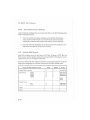
The following is a table of cache configurations and suggested speed ratings
of the SRAM for implementing the cache data RAM for various speeds of the
80486 CPU.
Cache Configuraion
2-1-2 Interleave *
25 MHz CPU 33 MHz CPU 50 MHz CPU
None
20 ns
20 ns
2-1-2 Non-interleave
20
ns
None
None
2-2-2 Non-interleave
20
ns
20
ns
None
3-2-3 Non-interleave
20
ns
20
ns
20
ns
ns
20
ns
3-2-3 Interleave
20
ns
20
N o t e : " * " x -y- z means x-y-y-y burst read and zT write cycle.
Interleave means two banks Cache (64KB/256KB)
Non-interleave means one bank Cache (128 KB).
SL 486VE
User's
Manual
32- Bit Slots
ш IM
IH 2
4
S7
Л , SB
S1
S2
S3
S4
S6
Banku
S6
Turob SW
#
1£3&3
Turbo LED
f~1 |W«
Reset Speaker KeyLock
Figure 3 . 1 SL 4 8 6 V E Board Layout
4-2
4
BankT,
Jumper Settings and Connectors
Chapter 3
Jumper Settings and Connectors
This chapter will assist you in setting up the SL 486VE before you install it in
a system case. If your SL 486VE has already been installed and you do not
wish to change the configuration settings, you can skip over this section.
3.1
Jumper Settings
The SL 486VE has several jumper switches that must be set to define a system
configuration. They are turned off and on by placing or removing a cover cap
over the pins. This is called an opened or a closed jumper. All jumpers must
be set to one of the possible two settings.
Figure 3.1 shows the location of the jumpers and connectors.
3-1
Jumper Settings and
Connectors
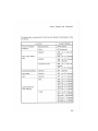
The table below summarizes the functions and settings of each jumper on the
SL 486VE.
Function
Jumper Setting
Monochrome
JP14closed
Color
JP14opened
486DX
JP8 pin 1,2 & 3,4
closed
JP9 pin 1,2 closed
486SX
JP8
JP9
OverDrive CPU
JP8 pin 1,2 & 2,3
closed
JP9 pin 2,3 closed
Local Burst Mode
Default
JP1
CPU Miss
Default
JP2 pin 2,3 closed
JP7
Default
JP7
64K
JP3 pin
JP4 pin
JPIOpin
JP11 pin
JP12 pin
JP13 pin
1,2
1,2
1,2
2,3
1,2
1,2
128K
JP3 pin
JP4 pin
JPIOpin
JP11 pin
JP12 pin
JP13pin
2,3 closed
1,2 closed
2,3closed
1,2 closed
1,2 closed
2,3 closed
Type of Display
Adapter
CPU Type Selection
Cache Memory
Size Setting
pin 2,3 closed
opened
opened
pin 1,2 closed
closed
closed
closed
closed
closed
closed
3-3
SL 486VE User's Manual
Function
Jumper Setting
Cache Memory
Size Setting
256K
VESA ID Selecton
CPU Speed > 33MHz JP5
CPU Speed< = 3 3 M H z JP5
closed
opened
1 Wait State Write
0 Wait State Write
closed
opened
3.2
JP3 pin
JP4 pin
JPIOpin
JP11 pin
JP12pin
JP13 pin
JP6
JP6
2,3
2,3
2,3
4,5
2,3
2,3
closed
closed
closed
closed
closed
closed
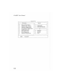
Connectors
There are several connectors located on the SL 486E. They are used to connect
with some peripheral devices to enhance the operating performance of the
system.
Refer to Figure 3.1 for the positions of all the connectors on the mainboard.
Their functions are listed below:
Connector
J1
4-4
Function
Keyboard Connector
J2
Power Supply
JP7
KeyLock Connector
JP6
Speaker Connector
JP5
Hardware Reset Connector
JP4
Turbo Switch Connector
JP3
Turbo LED Indicator
SL 486VE User's Manual
to operate according to this information. If the information it retrieves is
incorrect or insufficient, the system may not be able to operate properly until
accurate information is supplied. You do this by means of the SETUP
program built in the system BIOS.
4.2.1
When Should You Run Setup ?
1.
Although someone may have set up the system for you,you may want
to adjust the system to fit your needs.
2.
Whenever you change some components in your system, (for example, if you add a hard disk or more memory), you must run Setup to
record the new system configuration. If you don't do so after adding
memory, the computer will prompt you to run Setup.
3.
The last and most unlikely possibility is the loss of information in the
CMOS memory. You may never encounter this situation. But if you
do, you can restore the information by running the Setup.
4.2.2
How to Recall the Setup Program ?
You can run the built-in SETUP program in several ways:
1.
When powering-on the system
When you turn on the system power or press the reset button on the
system case while the system is running (not every system has this
button), the BIOS will first test the functionality of the system
components and display a start-up message similar to the following:
XXXX KB OK
Hit <Del>,If you want to run Setup
The numeral digits will continue to count at the top left of the screen.
This represents the BIOS testing the mainboard memory chips.
Before the above message disappears, you can press the < D e l >
key to run the Setup program.
2.
To reset the system
By pressing < C t r l > < Alt > < D e l > key combination when the
system is up and running (assuming you are running under DOS or
other environments that support this feature), the system will immediately reset itself and boot up. Before booting up from a diskette or
hard disk, you can also see the below start-up message :
Hit <Del>,if you want to run Setup
4-2
Built-in BIOS Setup Program
Chapter 4
Built-in BIOS Setup Program
This chapter provides detailed instructions on how to configure your system
using the Built-in BIOS Setup program and gives some technical information
about your computer. If you are not very familiar with microcomputers,
please read this chapter carefully before proceeding. If you do not want to
change the system's configuration, you can skip this chapter.
Before you start to add optional devices to your system, you should first learn
how to set up your system and adjust its jumpers (Refer to Chapter 3 for
detailed information). You may run the Setup program of the SL 486VE only
after all jumper setting adjustments have been completed. At this time you
should record what the configuration is, and keep it for reference.
4.1 Setup Summary
1.
2.
3.
4.
5.
6.
7.
Install any extra memory SIMMs.
Set jumper JP14 for color or monochrome monitor.
Make all connections to board.
Install control cards, monitor, and any peripheral devices and drivers.
Turn on system.
At setup prompt, press the Del key.
Type the password if you set the password checking option to "Setup" or
"Always" in the Advanced CMOS Setup program.
8. Choose Standard CMOS, Advanced CMOS or Advanced Chipset Setup.
9. Follow screen prompts.
4 . 2 BIOS Setup
Every AT-compatible computer has battery supported CMOS memory otherwise called "non-volatile "RAM. It stores information about your computer
and peripheral device configuration. Unlike ordinary RAM, it retains the
information even after you turn off your computer.
A computer needs to know certain things about itself so it can operate
correctly when powered on. A special type of software called BIOS (Basic
Input Output System) is contained in read-only memory (ROM) chips on
the mainboard. The BIOS reads information from the CMOSmemory every
time you power on the computer. It then instructs the CPU and other devices
4-1
Built-in BIOS Setup Program
3.
When the BIOS prompts you
In the self-test process, if the BIOS detects inconsistent or incorrect
configuration information or some physical system error, it will
display an error message on the screen, and prompt you to take
action; for example:
Run SETUP UTILITY
Press <F1> to RESUME
Press the < F 1 > key,and continue.
4.
4.2.3
To Enter password
If you set the password checking option to the "Setup" or "Always"
field in the Advanced CMOS Setup program, after pressing the
"Del" key to run the Setup program, the Enter password message
will be displayed on the screen. Refer to section 4.6, Using the
Change Password Setup.
Running the SETUP Program
When you call up the Setup program, the screen displays a "main menu"
similar to the following:
BIOS SETUP PROGRAM - AMI BIOS SETUP UTILITIES
(C) 1991 American Megatrends Inc., All Rights Reserved
STANDARD CMOS SETUP
ADVANCED CMOS SETUP
ADVANCED CHIPSET SETUP
AUTO CONFIGURATION WITH BIOS DEFAULTS
CHANGE PASSWORD
WRITE TO CMOS AND EXIT
DO NOT WRITE TO CMOS AND EXIT
Standard CMOS Setup for Changing Time, Date, Hard Disk Type, etc.
ESC:EXIT 4- — : S e l F2/F3:Color F10:Save&Exit
Figure 4.1 BIOS Setup Main Menu Options
On-screen instructions at the bottom of the screen explain how to use the
program.
4-3
SL 486VE User's Manual
The following is a brief description of the six options of the Setup main menu:
•
STANDARD CMOS SETUP
Display the standard CMOS Setup screen to check or modify general
configuration information. The standard CMOS setup displays the date,
time, floppy type, hard disk type, video type, etc.
•
ADVANCED CMOS SETUP
The ADVANCED CMOS SETUP option is used to set the various system
options for the user, including the above 1 MB memory test, scratch RAM
area for BIOS, coprocessor detection, video ROM shadowand system ROM
shadow.
И
ADVANCED CHIPSET SETUP
This Setup option is for the user who wishes to program the chipset registers.
The chipset registers control most of the system options in the computer.
•
AUTO CONFIGURATION
WITH BIOS DEFAULTS
This option allows for automatic configuration of all the options in the
Advanced CMOS Setup/Advanced Chipset Setup with the BIOS defaults.
•
CHANGE PASSWORD
The password is required for entering the Setup program or booting your
system. The user can change the current password stored in the CMOS by
accessing this option.
13 WRITE TO CMOS AND EXIT
Choose this option to save the changes you have made in the "Standard
Setup"," Advanced Setup" and "Advanced Chipset" options, and then exit
to reboot the system.
•
DO NOT WRITE TO CMOS AND EXIT
Choose this option to abandon all previous settings and then exit to reboot
the system.
To choose an item from the Setup main menu, move the cursor to appropriate
line using the Up < t > and Down < i > arrow keys and press < E n t e r > .
The screen will display a warning message as below:
4-4
Built-in BIOS Setup Program
BIOS SETUP PROGRAM-WARNING INFORMATION
(C) 1991 American Megatrends. Inc., All Rights Reserved
Improper Use of Setup May Cause Problems!!
If System Hangs, Reboot System and Enter Setup by Pressing the < D e l > Key
Do Any of the Following After Entering Setup
(i) Alter Options to Make System Work
(ii) Load BIOS Setup Defaults
(iii) Load Power-On Defaults
Hit < E S C > to Stop Now, Any Other Key to Continue
Figure 4.2 BIOS Setup Warning Message
4.3 Running the Standard CMOS Setup
To check or modify the general system configuration, choose "STANDARD
CMOS S E T U P " from the Setup main menu and press < Enter > .The screen
will display the following:
BIOS SETUP PROGRAM - ADVANCED CMOS SETUP
(C) 1990 American Megatrends Inc., All Rights Reserved
Base m e m o r y
Ext. m e m o r y
Date (mn/date/year): Tue, Jan 01, 1980
Time (hour/min/sec): 01 : 19 : 01
Hard disk C: type:
Hard disk D: type:
Floppy drive A:
Floppy drive B:
Primary display:
Keyboard:
47 = USER TYPE
Not Installed
1.2 MB, 5 1/4"
Not Installed
VGA/PGA/EGA
Installed
Month : Jan, Feb,
01, 02,03
Date
1901, 1902,
Year
Dec
31
2099
: 640 KB
: 256 KB
Cyln Head W p c o m LZone Sec Size
981
10
17
81 MB
Sun
Mon
Tue
Wed
Thu
Fri
Sat
30
31
1
2
3
4
5
6
7
8
9
10
11
12
13
14
15
16
17
18
19
20
21
22
23
24
25
26
27
28
29
30
31
1
2
3
4
5
6
7
S
9
t i - » T ^ S e l e c t F2/F3:Color PU/PD:Modify
Figure 4.3 The Standard CMOS Setup Program Screen
4-5
SL 486VE User's Manual
On-screen instructions in the lower left corner of the screen explain how to
use the program. After making all selections, press < E S C > key and then
return to the main menu program to choose another Setup program.
И
Date
In the Date fields, you manuallyset the electronic calendar on the mainboard
only if the values are incorrect.
И
Time
Time fields include hour, minutes, seconds, but you can only set the value of
hour and minute. Check and adjust these fields according to your clock or
wrist watch.
И
Floppy Drive A and В
In this field you may specify the capacity and format of the floppy drives
installed in your system.
В
Hard Disk С: and Hard Disk D:
In these fields, you specify the physical and electronic properties of the
"standard" hard disk drives installed in your system. Relevant specifications
include the number of cylinders and heads, write pre-compensation time,
read/write head landing zone, number of sectors per track.
The BIOS provides 46 predefined types of popular hard disk drives. You
select the appropriate type by scrolling forward/backward using the
< P g U p > and < P g D n > keys. The relevant specifications of the selected
drive will be immediately displayed on the corresponding field positions.
If for some reasons your particular drive is not one of the 46 predefined types,
simply scroll down to select type 47, then use the left <<— > and right <—»
arrow keys to move to the Cyln(Cylinders), Head, WPcom(Write Pre-Compensation),LZone(Landing Zone),and Sec(Sectors) fields and directlykey
in the appropriate values. The Setup program will calculate the capacity of
the drive based on the input cylinder, head and sector numbers and display
the result on the capacity field for your reference.
Refer to Appendix A for the table of hard disk types.
•
Primary Display
In the display field, you specify the display adapter installed in your system.
•
Keyboard
This setting is used to select "Installed" or "Not Installed" for the keyboard
during the Power On Self Test. Normally, it should be set as "Installed".
4-6
Built-in BIOS Setup Program
Щ
Base Memory and Extended Memory
A small section in the upper right corner of the screen displays important
status information on your system, including base and extended memory
amount. They are updated automatically by the Setup program according to
status detected by the BIOS self-test; no manual change is allowed.
4.4 Running the Advanced C M O S Setup
When you choose.the "RUN Advanced CMOS Setup" option in the Setup
main menu, the screen displays the following menu:
BIOS SETUP PROGRAM- ADVANCED CMOS SETUP
(C)1991 American Megatrends Inc., All Rights Reserved
Above 1 MB Memory Test
Hard Disk Type 47 RAM Area
System Boot Up N u m Lock
External Cache M e m o r y
Internal Cache M e m o r y
Password Checking Option
Video ROM S h a d o w С 0 0 0 . 3 2 К
:
:
:
:
:
:
:
Disabled
DOS 1KB
On
Enabled
Enabled
Setup
Enabled
ESC:Exit 4- —»t <—: Sel (Ctrl)Pu/Pd:Modify F1:Help F2/F3:Color
F5:0ld Values F6:BI0S Setup Defaults F7:Power-On Defaults
Figure 4 . 4 T h e Advanced CMOS Setup Program Screen
Above 1 MB Memory Test
П
You can disable this option to bypass the memory test if a lot of memory is
installed in the system, or you can enable this option to test all the memory.
•
Hard Disk Type 47 RAM Area
The purpose of this field is to specify the address of the memory area used
by the system BIOS for storing extended information, such as to save the user
definable drive type 47.
You have the following options:
.
0:300
To reserve the stack area at address 30h:0.
4-7
SL 486VE User's Manual
• DOS 1KB
To reserve the top 640 KB in the DOS base memory and reduce the
size of base memory by 1 KB.
H
System Boot Up Num Lock
This option can set the "Num Lock" key to "On" or " O f f ' a f t e r system boot
up.
H
External/ Internal Cache Memory
Due to constraint of technology, speed of currently available D R A M may
not be high enough to catch up with the speed of the CPU, which means that
at every step of program execution, the CPU must wait for the DRAM to
respond.
In fact, for CPU to run faster, the system must be designed to use another
kind of fast RAM chip — S R A M (Static-column RAM).
You can have a dual cache architecture - internal (from the CPU) & external
cache (from the SRAM).
И
Password Checking Option
The purpose of this field is to determine whether the password is asked for
in every boot (set to "Always") when entering into the Setup program (set to
"Setup") or never asked for (set to "Disabled").
•
Video ROM Shadow
Choose these two options for better video display performance. It enables
the shadow RAM operation for the video BIOS on display cards such as
VGA or EGA. The video card should be checked to see whether it has 16 К
or 32 К of R O M .
4-8
Built-in BIOS Setup Program
4.5 Running the Advanced Chipset Setup
To program the registers of the chipset, choose the "Advanced Chipset
Setup" option from the Setup main menu and press < E n t e r > . T h e screen
will display the following menu:
BIOS SETUP PROGRAM - ADVANCED CHIPSET SETUP
( O 1 9 9 0 American Megatrends Inc., All Rights Reserved
Auto-Configuration
: Enabled
DRAM Speed
: Slowest
DRAM Write CAS pulse Width : 2T
Cache Write Back
: Disabled
Cache Write Cycle
: 3T
Cache Burst Read Cycle
: 1T
BUSCLK Selection
: 7.159MHz
Non-Cacheable Area 1
: DRAM
Non-Cacheable Area 1 Size
: 0 KB
Non-Cacheable Area 1 Start
: Disabled
Non-Cacheable Area 2
: DRAM
Non-Cacheable Area 2 Size
: 0 KB
Non-Cacheable Area 2 Start
: Disabled
С ООО Shadow RAM Cacheable : Disabled
F000 Shadow RAM Cacheable : Disabled
DRAM Hidden Refresh
: Disabled
I/O Recovery Select
: 11 BCLKs
ESC: Exit Sel (Ctrl) Pu/Pd: Modify F1: Help F2/F3: Color
F5: Old Values F6: BIOS Setup Defaults F7: Power-On Defaults
Figure 4.5 The Advanced Chipset Setup
И
Auto-Configuration
If enabled, following parameters will be automatically configured with values
depending on CPU clock speed:
. DMA Speed
. DRAM Write CAS Pulse Width
• Cache Write Cycle
• Cache Burst Read Cycle
• BUSCLK Selection
If disabled, user selected values for above parameters will be used. The
available options are listed below:
•
•
Disabled
Enabled
4-9
SL 486VE User's Manual
•
DRAM Speed
There will be plenty of timing marging if the user adopts Fastest for 25 MHz,
Faster for 33 MHz, and Slowest for 50 MHz, even when 100ns D R A M s are
used. If 70/ 80ns DRAMs are used, faster speed option can be selected.
•
DRAM Write CAS Pulse Width
The option determines the number of wait states to be kept when the CPU
writes data into the local DRAM.
The available options are as follows:
.
2 T
.
IT
Ш
Cache Write Back
I f disabled, cache is write-through. If enabled, cache is write-back. A writeback cache can offer higher performance than a write-through if writes to
the main memory are much slower than writes to the cache. The write-back
cache is also favored when a memory location is written several times in the
cache before written into the main memory. The performance advantage of
the write-back cache over write-through cache is software dependent.
•
Cache Write Cycle
During CPU cycle, it is used as a write latch function to support longer data
hold time for DRAM write, while in hold acknowledge cycle it indicates
cache read hit.
•
Cache Burst Read Cycle
Due to constraint for technology, speed of currently available SRAM may
not be high enough to catch up with the speed o f t h e CPU, which means that
at every step of program execution, the CPU must wait for the SRAM to
respond. This option determines the number of cycle times to be inserted
when CPU read data to SRAM.
Moreover, the setting depends on the speed of the CPU and SRAM. I f the
CPU is of high speed, the timing of SRAM processing data needs an
extension, except for some SRAMs that can be high enough to catch up with
the speed of CPU .
The available options are as follows:
«
2-1-1-1
. 3-1-1-1
о 3-2-2-2
4-10
Built-in BIOS Setup Program
•
BUSCLK Selection
The BUSCLK Selection is an output clock for the I/O channel. This field
used to specify the I/OBUSCLK clcok source used by the system. The user
does not need to change this settings.
The available options are listed below:
. 7.159MHz
. CPUCLK/2 (is
• CPUCLK/2.5
. CPUCLK/3 (is
. CPUCLK/4 (is
. CPUCLK/5
• CPUCLK/6 (is
. CPUCLK/8
•
recommended for 16 & 20 MHz)
recommended for 25 MHz)
recommended for 22 MHz)
recommended for 50 MHz)
Non-Cacheable Area 1/2
In some applications, users desire a block of memory not to be cached. The
mainboard provids two programmable non-cacheable regions to serve this
function. The memory residing on the AT add-on is non-cacheable. When a
memory space is mapped by both the on-board DRAM and AT add-on
memory, CPU access will be conducted to the on-board D R A M . If users
desire the AT add-on memory to be accessed instead of the on-board D R A M
at the overlapped memory space, the two non-cacheable regions can be used
to disable the on-board DRAM in the proagrammed space.
H
Non-Cacheable Area 1/2 Size
For some special I/O cards which need to use system memory, you should
reserve some memory space for use. The size of the Non-Cacheable Area
1/2 can be as small as 64KB or as large as 4MB. The Non-Cacheable Area
1/2 Start is set to be "Disabled" as default value.
•
Non-Cacheable Area 1/2 Start
This function is to set the address of Non-Cacheable Area 1/2 from starting.
•
C000 Shadow RAM Cacheable
If you have a shadowing of the video BIOS at C000 Shadow RAM, you can
enable this memory cacheable.
•
FOOO Shadow RAM Cacheable
If you have a shadowing of the system BIOS, you can enable this option for
memory cacheable function.
4-11
SL 486VE User's Manual
Я
DRAM Hidden Refresh
Recently the speed of DRAM is becoming faster so the time needed per
refresh cycle is getting shorter. The refresh cycle time for the 100ns DRAM
is 200ns minimum, for example. In a system with cache, most of the CPU
accesses are referred to the cache so that the DRAM usage (percent of time
the D R A M is accessed by the CPU) is significantly reduced.
В
I/O Recovery Select
This field is used to specify the I/O command recovery time except for some
add-on card that cannot work properly. It is recommended to set this option
at low" value to enhance the I/O performance.
The available options are as follows:
о
.
.
.
3 BCLKs
4BCLKs
5BCLKs
11 BCLKs
4.6 Using the Change Password Setup
To change the password.choose the "ГН ANOF PASSWORD"option from
the Setup main menu and press < Enter > .
1.
If the CMOS is bad or if this option has never been used, the user is
asked to enter new password. The screen will display the following
message:
Enter NEW Password:
If you want to disable the password function, you can press < E n t e r > key to return to the Main Setup menu.
2.
If the CMOS is good or if this option has been used to enter the
password, the user is asked for the password stored in the CMOS.
The screen will display the following message:
Enter Current Password:
Enter the correct password and continue to change the password.
4-12
Built-in BIOS Setup Program
After pressing the current password , you can change the password stored
in the CMOS. The password can be at most 6 characters long.
To change the password, please follow the steps below:
4.7 BIOS Errors and Messages
After entering setup choices, the system will reboot. The setup summary and
system information will appear on screen along with messages. These may
include ERROR messages concerning the system or setup.
AMI BIOS performs various diagnostic tests at the time the system is turned
on. Whenever an error is encountered during these tests, there will be either
a few short beeps or an error displayed on the monitor. If the error occurs
before the display device is initialized, the system reports the error with
several short beeps.
If the error is FATAL, the system halts after reporting the FATAL error. If
the error is NON-FATAL, the process continues after reporting the error.
4-13
SL 486VE User's Manual
4.7.1
Fatal Errors Through Beeps
These errors are conveyed through a number of beeps.
Beep Count
1
2
4
5
6
7
9
4.7.2
Meaning
DRAM Refresh Failure
Base 64 KB RAM Failure
System Timer Failure
Processor Failure
Keyboard Controller-GATE A20 Error
Virtual Mode Exception Error
ROM-BIOS C h e c k s u m Failure
Non- Fatal Errors Through Beeps
These errors are conveyed as one long beep followed by several short beeps.
Beep Count
3
8
4.7.3
Meaning
Conventional and Extended Memory Test Failure
Display Test and Vertical and Horizontal Retrace Test Failure
Fatal Errors Shown in Display
When these errors are displayed, the screen is cleared,and the error message
display is followed by a line saying SYSTEM HALTED.
1.
CMOS INOPERATIONAL: indicates failure of CMOS shutdown
register test.
2.
8042 GATE-A20 E R R O R : error in getting into protected mode.
3.
INVALID SWITCH MEMORY FAILURE
4.
DMA E R R O R ; DMA controller page register test failed.
5.
DMA # 1 E R R O R : DMA Unit 1 register test failed.
6.
DMA # 2 E R R O R : DMA Unit 2 register test failed.
4-14
Built-in BIOS Setup Program
4.7.4
Non- Fatal Errors In Display
There are two types of errors in this category:
1.
One that requires you to press the F1 key and give you the option of
running SETUP.
2.
One that requires you to press the F1 key and don't give you the
SETUP option.
4.7.5
Errors With Setup Option
1.
CMOS battery state low indicates failure of CMOS battery or a
failure in the set and checksum tests.
2.
CMOS system options not set indicates failure of CMOS battery or
a failure in the set and checksum tests.
3.
CMOS checksum failure indicates CMOS battery low or a failure in
the set and checksum tests.
4.
CMOS display type mismatch indicates failure of display verification.
5.
CMOS memory size mismatch indicates system configuration and
setup failure.
6.
CMOS time & date not set indicates system configuration verification error and setup error (in timer).
4.7.6
Errors Without Setup Option
1.
CH-2 timer error indicates channel 2,1,0 timer test failure.
2.
keyboard error indicates keyboard test failure.
3.
KB/Interface error indicates keyboard test failure.
4.
Display switch setting not proper indicates display type verification
error.
5.
Keyboard is locked ....Unlock it.
6.
FDD controller error indicates system configuration verification
error in diskette setup.
7.
H D D controller failure indicates system configuration verification
error in hard disk setup.
8.
C:Drive error indicates hard disk setup error.
9.
D:Drive error indicates hard disk setup error.
10. D:Drive failure indicates hard disk failure.
4-15
EISA Configuration Utility
Chapter 5
EISA Configuration Utility
The EISA Configuration Utility software utility from American Megatrends, Inc. configures EISA (Extended Industry Standard Architecture)
computer systems.
EISA systems and adapter cards are much more complex and flexible than
the older ISA designs. The EISA configuration Utility was created to automate this configuration process in EISA systems.
The E C U permits the user to configure an EISA computer. The E C U takes
into account the needs of all adapter cards in the system. The E C U configures the EISA devices and sets and maintains system parameters, storing
them in EISA CMOS R A M . The ECU guarantees that there will be no
conflicts or contention issues between adapter cards, since it assigns all
necessary system resources.
The E C U must be executed every time ISA or EISA adapter cards are
physically added, removed, or moved. The E C U operates on the information
provided by the CFG (configuration) files that accompany the EISA motherboard and EISA or ISA adapter cards.
5.1
EISA Specification
EISA is an acronym for Extended Industry Standard Architecture. EISA is
basically a superset of the Industry Standard Architecture (ISA), which is
based on IBM's original PC/AT specifications. The EISA specifications
allow 32-bit memory addressing to be used by the CPU, D M A devices, and
bus mastering devices. The above devices can also use either 16-bit or 32-bit
data transferring.
5.1.1
EISA/ISA Differences
An important different between ISA and EISA is that in EISA systems,
configuration is done through software, rather than the hardware switches
5-1
SL 486VE User's
Manual
used by an ISA system. In other words, I/O ports, R O M addresses, memory
use, and the IRQ and DMA lines for an EISA motherboard and adapter
card are configured using an E C U , where an ISA card uses DIP switches
and jumpers to perform the same function.
5.1.2
EISA Bus Specification
The EISA computer has 32-bit expansion slots that are fully compatible with
8-bit and 16-bit PC/XT/AT expansion slots. EISA expansion slots have 188
pins. The upper 98 pins are exactly the same as the standard AT pinouts. The
lower 90 pins are used for EISA bus signals.
The EISA bus is much faster than the ISA Bus. Not only does EISA provide
a wider 32-bit bus, it also provides a maximum 33 MB/sec bus transfer rate.
An ISA bus can transfer data at only 8 MB/sec. EISA achieves this higher
throughput using high-speed burst mode transfers, which take only one clock
cycle. Normal (ISA compatible) transfers take two clock cycles.
EISA Bus Rate Versus the ISA Bus Rate
Attribute
EISA Bus
ISA Bus
Burst Transfer Rate
33 MB/sec
8 MB/sec at 0 wait states
DMA characteristics
Supports 8, 16, and 32-bit
DMA
Supports 8 and 16-bit
DMA
DMA Transfer Rate
33 MB/ sec
1 to 4 MB/seo
Adapter Card Pin Count
188 pins
98 pins
Bus Master
Intelligent Bus Master
No Bus master
Configuring Adapter
Cards
Auto configuration
through ECU.
DIP svutch and j u m p e r
setting still available.
Only DIP Switch and
jumper
setting available.
5.1.3
EISA Configuration Utility Features
A practical benefit of EISA is automatic configuration of system resources
and adapter cards. That means an end to DIP switches, jumpers, and
4-2
EISA Configuration Utility
installing configuration files, although switch configurations are still allowed
for both ISA and EISA to maintain compatibility.
EISA provides a product identification mechanism for system and adapter
cards. The computer automatically interrupts each device during the BIOS
Power-On Self Test (POST) for the product identifier, compares it with the
ID stored in EISA Extended CMOS RAM and configures the adapter card
accordingly.
The EISA configuration scheme has the following characteristics:
•
An ECU (EISA Configuration Utility) for configuration of motherboards and adapter cards.
• A software interface to the ECU used by CFG files to control the
configuration process.
. CFG files for the ECU.
• CFG files for the motherboard and adapter cards.
• EISA Extended CMOS RAM to store configuration parameters.
® A mechanism to save and restore the configuration parameters.
о BIOS routines to read and write to Extended CMOS RAM.
о Automatic detection and initialization of adapter cards by the
BIOS during POST routines.
• 1 KB of I/O address space for each EISA expansion device (adapter card).
5.2
Configuring Your Computer for the First Time
The first time you set up your EISA computer and any time you change the
configuration by adding or removing an EISA or ISA board, you must
configure your system with the EISA Configuration Utility program. When
the configuration process is completed, the configuration is stored in the
computer's nonvolatile memory where it is available to the system whenever
you use your computer.
The EISA Configuration Utility program is on the System Configuration
diskette provided with your computer. Before you use this diskette to run the
Configuration Utilityprogram,we recommend that you make a backup copy.
This ensures that you will be able to run the program if the original diskette
is damaged or lost.
5-3
SL 486VE
5.3
User's Manual
Installing the ECU
The E C U is easy to install and can be used from either a hard disk drive or
a floppy drive.
Hard Disk Drive Operation
Simply copy all files from the ECU floppy disk to the same directory on the
hard disk drive. Make sure all CFG files are copied to the same directory.
Floppy Drive
You can execute the ECU from a floppy drive.
Make a backup copy of the AMI E C U floppy disk to use as a working copy.
You may have to run the ECU from a floppy drive if the system hard disk
drive must be configured by the ECU before it can be used.
System Requirements
The following are the minimum hardware and software requirements necessary to successfully use the E C U :
•
.
•
MS-DOS Version 3.2 or later
640 KB of R A M Memory
1.2 MB Floppy disk Drive and a hard disk drive, monitor and keyboard.
EISA Configuration Files
The E C U floppy disk should contain the following files:
. CFG .EXE the ECU (EISA Configuration Utility)
. EISACFG.HLP E C U Help file
• Several CFG files for ECS products.
Additional file can be created as the ECU is executed.
•
о
4-4
the CFG .ISA file is created when any ISA adapter card is configured
.CMS files are created in the EISA configuration process, as are
.INF files.
EISA Configuration Utility
CFG Files
Each adapter card in the EISA system should come with a CFG file on
floppy disk. A card's CFG file contains detailed information on the card
as well as the functions that the card can perform. The CFG file tells the
E C U the possible configuration choices for the adapter card and the
system resources that the adapter card needs. System resources include
BMA(Direct Memory Access) channels,IRQ (Interrupt Request) lines,
I/O Address Ports, and m e m o r y s p a c e . B e s u r e a l l C F G files for all cards
in the system and the CFG file for the motherboard are available before
running the E C U .
CMS File
The CMS file contains a copy of the configuration information that is
written into the system's Extended CMOS Memory. The default name
for a CMS file matches the ID of the system board that was used in the
configuration. Each CMS file should have a corresponding INF file.
SNF File
The INF file contains detailed information about a configuration such as
switch and jumper settings, software statements, connection statements,
and resource allocation. The INF file is used by the "Display/Print"
command to recall information on a saved configuration. Each INF file
should have a corresponding CMS file.
Pi
Running the EISA Configuration Utility
The E C U operates on the information provided by the CFG (Configuration)
files that accompany the EISA mainboard and EISA or ISA adapter cards.
The E C U stores configuration data in a battery-backed EISA Extended
CMOS R A M . When an EISA system is powered on, the BIOS reads this
configuration information and initializes all adapter cards in the system. If
the battery runs down, the contents of CMOS R A M can be lost. You must
then either reconfigure the system or copy the configuration data to EISA
Extended CMOS R A M from a backup source.
5-5
SL 486VE User's Manual
5.4.1
Main Menu
The main menu outlines the six steps involved in configuringan EISA system.
Steps 1,2, and 3 are optional. To select a step, use the up and down cursor
keys to move to a step and then press < Enter > .You may also select a step
by pressing its item.
The following sample screen shows the ECU Main Menu.
EISA CONFIGURATION UTILITY, Release 2.01
p5j> b .flout Ш
iitB%n:afbu
Step 2: Add and Remove Boards
Step 3: Change Configuration Settings
Step 4: Save Configuration
Step 5: View Switch/Jumper Settings
Step 6: Exit
[ S e l e c t = Enter
[Exit = ESC]
[Help = F1]
[Utilities = F9J
Step 1
About EISA Configuration
This step displays information for users who are new to
EISA and EISA configuration.
Step2
Add and Rempve Boards
This step is optional. Use this step to manuallyadd or delete
boards. Most boards are automatically detected and
added by the E C U .
Step3
Change Configuration Settings
This step is optional. Use this step to change configuration
settings for any board in the system. If you skip this step, all
setting will remain set to their default state.
Step4
Save Configuration
This step saves the configuration^ettjng to EISA CMOS
RAM and into a backup file (the CMS File).
Step5
View Switch/Jumper Settings.
This step displays h ę w t o set DIP switches and jumpers on
any board that is switch or jumper configurable.
4-6
EISA Configuration Utility
Step6
5.4.2
Exit
This step exits to the operating system. If any configuration
settings were changed, you are given the option o f rebooting the system so that the new settings will take effect.
Using Help
The help window may be accessed at any time by pressing the < F 1 > key
While in the help system you may scroll the window up and down using the
up and down cursor keys.
The help window includes a menu with three buttons at the bottom of the
window:
About AMI E C U Step2 (Add and Remove Boards)
Step3 (Change Configuration Settings)
Step4 (View Switch/Jumper Settings)
Step5 (Exit)
Back
Press F2 to redisplay the last help topic that was shown.
Contents
Press F3 to display the table of contents for the help system
help system.
Quit
Press ESC to exit from the help system and return to the
ECU.
5-7
SL 486VE User's Manual
5.5
About EISA Configuration
Use the cursor keys to move the menu bar to the "Step 1 "item and then press
. The screen will display the following:
About EISA Configuration and AMI E C U
The EISA Configuration Utility from American Megatrends, Inc.
configuresEISA (Extended IndustryStandard Architecture) computer
systems
EISA systems and adapter cards are much more complex
See also: CFG Files
CMS File
I N F File
Using Help
EISA CMOS RAM
EISA Slot Numbers
Main Menu
[Back= F2] [Contents= F3] [Quit= ESC]
There are several options available from the file menu.
CFG Files
The CFG file describes the adapter card characteristics and the system
resources that it requires. The CFG file should be on a floppy disk provided
with the EISA motherboard or EISA adapter card.
CMS File
The CMS file contains a copy of the configuration information that is written
into the system's EISA CMOS RAM. Each CMS file should have a corresponding INF file.
INF File
The I N F file contains detailed information about a configuration such as
switch and jumper settings, software statements, connection statements, and
resource allocation.
4-8
EISA Configuration Utility
EISA CMOS RAM
Initialization and configuration information is read by the E C U and stored
in EISA CMOS R A M . A backup of CMOS R A M configuration data is also
stored on disk. When the system is rebooted, the BIOS reads the CMOS
R A M configuration data and executes the initialization instructions during
POST.
EISA Slot Numbers
Each adapter card (EISA or ISA) is installed in an EISA or ISA expansion
slot (connector) on the EISA motherboard. The slots are numbered from 1
to n (n can be 1 through 15). The EISA motherboard is always slot 0.
5-9
SL 486VE User's Manual
5.6
Add and Remove Boards
The ECU is menu-driven for ease of installation. There is also an extensive
online help facility which can be accessed at any time by pressing the
< F 1 > k e y or by moving the cursor to the Help option at the top of the Main
Menu screen.
Use the cursor keys to move the menu bar to the "Step 2" and then press
< Enter > . The screen will display the following:
System - SL486VE EISA System Board
Slot 1 - Empty
Slot 2 - E m p t y
Slot 3 - Empty
Slot 4 - E m p t y
Slot 5 - E m p t y
Slot 6 - Empty
Slot 7 - E m p t y
Slot 8 - Empty
- Press INSERT to add a board that was not detected or has
not been installed yet.
- Press D E L to remove the selected board.
- Press F7 to move the selected board to a different slot.
- Press ESC when finished with this step.
[Select= ENTER] [Done=ESC] [Advanced Options=F9]
The Add and Remove Boards Screen allows you to edit the adapter card
configuration settings. You can change junction choice settings and resource
allocation settings by highlighting the adapter card to be modified and
pressing < Enter >
4-10
EISA Configuration Utility
5.6.1
Change Configuration Settings
When you choose a configuration setting to change by moving the cursor to
the appropriate adapter card and pressing < Enter > , the following screen
appears:
я м тел M B ^ r f
Slot 1 - Empty
Slot 2 - E m p t y
Slot 3 - Empty
Slot 4 - Empty
Slot 5 - Empty
Slot 6 - Empty
Slot 7 - Empty
SlotS - Empty
- This step is optional, you may skip it by pressing ESC and all
configuration settings will remain unchanged.
- Press ENTER to view or change a board's configuration settings.
- Press ESC when you are satisfied with the current settings.
[Select = E N T E R ] { D o n e = E S C ] [Advanced options=F9]
To change a function's choice setting, select one of the long horizontal bars
on the screen and press < Enter > . To change resource allocation settings,
select one of the shorter bars along the right edge of the screen. Select
< O K > or press < E s c > when you are finished editing this adapter card.
5-11
SL 486VE User's Manual
5.6.2
View Switch/Jumper Settings
After saving the configuration, it is important that you do the following steps
before using this system:
1. Note the switch and jumper settings and verify that all switches
and jumpers on the boards in your systems set correctly. Some
boards have switches and jumpers that need to be set manually.
2. Note the software statements to see if any of the boards in your configuration need special drivers to be loaded.
5.7
Define ISA Board
Most ISA adapter cards do not have a CFG file. Without a CFG file, the
E C U cannot reserve system resources automatically for ISA adapter cards.
These cards must be configured manually.
The chart below lists the resources used by common ISA adapter cards and
helps avoid assigning one of these resources to an EISA adapter card.
Type of ISA Adapter Card
!RQ
I Floppy Disk Controller:
6
'j Serial Ports:
4
3
4
3
СОМ1:
COM2:
COM3:
COM4:
DMA
Ports
2
3F0h-3F7h
-
3F8h-3FFh
3F8h-2FFh
3E8h-3EFh
2E8h2EFh
| Parallel Ports:
LPT1:
LPT2:
Other:
Other:
4-12
7
5
-
378h-37Fh
278h-27Fh
EISA Configuration Utility
Use the chart as a worksheet and list any other ISA adapter cards.
You can configure the system automatically or manually. If the system has
an ISA adapter cards and there is not a CFG file for each adapter card, use
Manual Mode to configure a system.
Manual Mode allows you to edit the configuration setting for all adapter
cards in the system and make sure there are no resource conflicts between
the EISA and ISA adapter cards.
Manual Configuration
5 1 о 1 0 - : Ш Ш Ш Ш шёшшж
Slot 1 - Empty
Slot 2 - Empty
Slot 3 - Empty
Slot 4 - Empty
Slot 5 - Empty
Slot 6 - Empty
Slot 7 - Empty
Slot 8 - Empty
[ Add]
[Remove]
[Move]
Щ1
Шшй
[Options]
[Save]
[Cancel]
You can also use the Display/Print option to show all resources used by the
EISA adapter cards in the system.
The above screen is displayed when configuring an ISA board. Complete the
screen as appropriate and choose Save to save this ISA Board definition.
This definition can be used in subsequent configuration sessions.
Choose Save to save this ISA Board definition. This definition can be used
in subsequent configuration session.
5-13
SL 4S6VE User's Manual
5.8
Check CFG File
Runs a syntax check on one or more CFG files and reports any errors. The
following sample screens depict the screens that can be displayed.
5.9
Write Ext C M O S
This option copies the contents of a CMS File to EISA Extended CMOS
R A M which is maintained by the battery when the system is turned off.Doing
this erases any previous configuration information stored in Extended
CMOS R A M . If there is more than one CMS File in the current directory, a
prompt asks which one to use. The following sample screen shows the
extended CMOS screen".
5.10 Board ID Map
This option displays a map of all EISA adapter cards in the system.
5.11 Other Main Menu Options
Display/ Print Menu
Board Functions
SL486VE EISA System Board
Resources
Basic Main Board Functions
1 llVltri
Reserved
Keai-time ы о с к
Reserved
Free
Free
Co-processor
[OK]
5-14
Installed
Link
101 Key
Link
EISA Configuration Utility
The Display/Print option presents a screen display of configured adapter
cards. The following screen appears. You can select any number of the listed
options to display.
The Display/Print menu has four group of options.
1.
The information to be displayed or printed. You can choose one or
more option.
2. The information source All Board or Selected Board. If you choose
Selected Board, a list of adapter cards is displayed.
3. The screen, printer (LPT1), or file. If you choose Tile," the E C U asks
for a DOS filename.
4. OK to display the information. Choose Cancel to return to the Main
Menu.
Choice Selection
Basic Main Board Functions
TIMER
Reserves IRQ, DMA and other resources
[ -4 ] Reserved
( O K ] [Cancel ]
Using Help
Help can be accessed at anytime by pressing < F 1 > or moving the cursor
to the Help option at the top of the Main Menu.
Quit
The last Main Menu option exits from the ECU and returns to DOS.
5-15
SL 486VE User's Manual
Display/Print
The configuration has been saved.
It is important that you do the follovung steps before
using this system:
1. View the switch and jumper settings and verify
that all switches and jumpers on the boards in
your system are set correctly. Some boards
have switches and jumpers that need to be set
manually.
2. View the software statements to see if any of
the boards in your configuration need special
drivers to be loaded.
Do you want to display or print configuration information ?
[ Yes ]
4-16
[ No ]
EISA Configuration Utility
ISA Board Definition
Board N a m e :
Manufacturer:
Board Type:
DMA
[ Save ]
Video Board
IRQ
[Load]
Slot Type: 16 Bit
Ports
Memory
[ New]
[ Delete ]
[ Quit]
5-17
SL 486VE User's Manual
File Selection
Select the CFG files to be checked.
Filespec *.CFG
[
[
] IECS1100.CFG - SI486VE EISASystem Board
] IECS1110.CFG - SL4S6VE EISASystem Board
[OK]
-[Cancel]
Pares Messages
Checking: IECS1110.CFG
Identified CFG file IECS1110.CFG
Board : SL4S6E EISASystem Board
C a t e g o r y : SYS
Parsing file : "IECS1110.CFG"
No errors detected
N u m b e r of warnings : 0
[ OK]
4-18
EISA Configuration Utility
Write Extended CMOS
This command vwites data to extended CMOS
from a CMS file. This will destroy any
previous configuration information that is
stored in the system's CMOS memory.
[OK]
[Cancel]
Display/ Print
Information
]
]
]
]
]
]
]
]
Board Information
Switches & Jumpers
Software Statements
Connection Statements
DMA Resources
IRQ Resources
Port Resources
Memory Resources
[OK]
Source
[
[
] All Boards
] Selected Boards
To
[
[
[
] Screen
] Printer
] File
[Cancel]
5-19
SL 486VE User's
Manual
Display/ Print
Information
]
]
]
]
]
]
]
]
Board Information
Switches & Jumpers
Software Statements
Connection Statements
DMA Resources
IRQ Resources
Port Resources
Memory Resources
[ OK ]
4-20
[ Cancel ]
Source
[
t
] All Boards
] Selected Boards
To
[
t
[
] Screen
] Printer
] File
Appendix A
Hard Disk Types
Type
Cylinders
Heads
WriteLanding
Precomp Zone Sectors
Capacity
(Mbytes)
1
306
4
128
305
17
10
2
615
4
300
615
17
20
3
615
6
300
615
17
31
4
940
8
512
940
17
62
5
940
6
512
940
17
47
6
615
4
65535
615
17
20
7
462
8
256
511
17
31
8
733
5
65535
733
17
30
9
900
15
65535
901
17
112
10
820
3
65535
820
17
20
11
855
5
65535
855
17
35
12
855
7
65535
855
17
50
13
306
8
128
319
17
20
14
733
7
65535
733
17
43
15
000
0__
000
000
17
00
16
612
4
0000
663
17
20
17
977
5
300
977
17
41
18
977
7
65535
977
17
57
19
1024
7
512
1023
17
60
20
733
5
300
732
17
30
Table A . I
AMI BIOS Hard Disk Types
A-1
Table A.1 AMI BIOS Hard Disk Types Continued
21
733
7
300
732
17
43
22
733
5
300
733
17
30
23
306
4
0000
336
17
10
24
325
7
0000
925
17
54
25
925
9
65535
925
17
69
26
754
7
754
754
17
44
27
754
11
65535
754
17
69
28
699
7
256
699
17
41
29
823
10
65535
823
17
68
30
918
7_
918
918
17
53
31
1024
11
65535
1024
17
94
32
1024
.15
65535
1024
17
128
33
1024
5
1024
1024
17
43
34
612
2
128
612
17
10
35
1024
9
65535
1024
17
77
36
1024
8
512
1024
17
68
37
615
8
128
615
17
41
38
987
3
987
987
17
25
39
987
7
987
987
17
57
40
820
6
820
820
17
41
41
977
5
977
977
17
41
42
981
5
981
981
17
41
43
830
7
512
830
17
48
44
830
10
65535
830
17
69
45
917
15
65535
_918_
46
1224
15
65535
1223
A-2
_
17
114
17
152
Appendix В
Setting the System Speed
There are two methods to select the system processing speed. You can
change the speed during operation while you are working with your application program.
High Speed
/
Ctrl
/
\
+
\
/
\
Alt
/
+
/
\
L o w Speed
Ctrl
*
+
Alt
/
+
" + " means one must press the keys simultaneously.
+
4
\