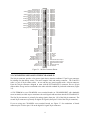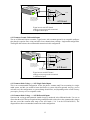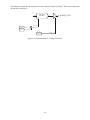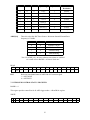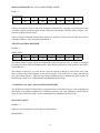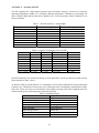
1
PCI-DAS1602/12 PCI Bus Data Acquisition Board User’s Manual Revision 4, September 2001 ME A S U R E M E NT CO MP U T I N G CO RP O RA T I O N LIFETIME WARRANTY Every hardware product manufactured by Measurement Computing Corp. is warranted against defects in materials or workmanship for the life of the product, to the original purchaser. Any products found to be defective will be repaired or replaced promptly. LIFETIME HARSH ENVIRONMENT WARRANTYTM Any Measurement Computing Corp. product which is damaged due to misuse may be replaced for only 50% of the current price. I/O boards face some harsh environments, some harsher than the boards are designed to withstand. When that happens, just return the board with an order for its replacement at only 50% of the list price. Measurement Computing Corp. does not need to profit from your misfortune. By the way, we will honor this warranty for any other manufacture’s board that we have a replacement for! 30 DAY MONEY-BACK GUARANTEE Any Measurement Computing Corp. product may be returned within 30 days of purchase for a full refund of the price paid for the product being returned. If you are not satisfied, or chose the wrong product by mistake, you do not have to keep it. Please call for a RMA number first. No credits or returns accepted without a copy of the original invoice. Some software products are subject to a repackaging fee. These warranties are in lieu of all other warranties, expressed or implied, including any implied warranty of merchantability or fitness for a particular application. The remedies provided herein are the buyer’s sole and exclusive remedies. Neither Measurement Computing Corp., nor its employees shall be liable for any direct or indirect, special, incidental or consequential damage arising from the use of its products, even if Measurement Computing Corp. has been notified in advance of the possibility of such damages. MEGA-FIFO, the CIO prefix to data acquisition board model numbers, the PCM prefix to data acquisition board model numbers, PCM-DAS08, PCM-D24C3, PCM-DAC02, PCM-COM422, PCM-COM485, PCM-DMM, PCM-DAS16D/12, PCM-DAS16S/12, PCM-DAS16D/16, PCM-DAS16S/16, PCI-DAS6402/16, Universal Library, InstaCal, Harsh Environment Warranty and Measurement Computing Corp. are registered trademarks of Measurement Computing Corp. IBM, PC, and PC/AT are trademarks of International Business Machines Corp. Windows is a trademark of Microsoft Corp. All other trademarks are the property of their respective owners. Information furnished by Measurement Computing Corp. is believed to be accurate and reliable. However, no responsibility is assumed by Measurement Computing Corp. neither for its use; nor for any infringements of patents or other rights of third parties, which may result from its use. No license is granted by implication or otherwise under any patent or copyrights of Measurement Computing Corp. All rights reserved. No part of this publication may be reproduced, stored in a retrieval system, or transmitted, in any form by any means, electronic, mechanical, by photocopying, recording or otherwise without the prior written permission of Measurement Computing Corp. Notice Measurement Computing Corp. does not authorize any Measurement Computing Corp. product for use in life support systems and/or devices without the written approval of the President of Measurement Computing Corp. Life support devices/systems are devices or systems which, a) are intended for surgical implantation into the body, or b) support or sustain life and whose failure to perform can be reasonably expected to result in injury. Measurement Computing Corp. products are not designed with the components required, and are not subject to the testing required to ensure a level of reliability suitable for the treatment and diagnosis of people. © Copyright 2001, Measurement Computing Corporation HM PCI-DAS1602_12.lwp Table of Contents . . . . . . . . . . . . . ................................................ 1 1.0 INTRODUCTION 1.1 FUNCTIONAL DESCRIPTION . . . . . . . . . . . . . . . . . . . . . . . . . . . . . . . . . . . . . . . . . . . . . . . . . . . . . . . 1 1.1.1 Analog Inputs . . . . . . . . . . . . . . . . . . . . . . . . . . . . . . . . . . . . . . . . . . . . . . . . . . . . . . . . . . . . . . . 1 1.1.2 Burst Mode . . . . . . . . . . . . . . . . . . . . . . . . . . . . . . . . . . . . . . . . . . . . . . . . . . . . . . . . . . . . . . . . 1 1.1.3 Analog Outputs . . . . . . . . . . . . . . . . . . . . . . . . . . . . . . . . . . . . . . . . . . . . . . . . . . . . . . . . . . . . . 2 1.1.4 Parallel Digital I/O . . . . . . . . . . . . . . . . . . . . . . . . . . . . . . . . . . . . . . . . . . . . . . . . . . . . . . . . . . . 2 1.1.5 Counter/Timer I/O . . . . . . . . . . . . . . . . . . . . . . . . . . . . . . . . . . . . . . . . . . . . . . . . . . . . . . . . . . . 2 2.0 INSTALLATION . . . . . . . . . . . . . . . . . . . . . . . . . . . . . . . . . . . . . . . . . . . . . . . . . . . . . . . . . . . . . . . . . . 3 2.1 SOFTWARE INSTALLATION . . . . . . . . . . . . . . . . . . . . . . . . . . . . . . . . . . . . . . . . . . . . . . . . . . . . . . . 3 2.2 HARDWARE INSTALLATION . . . . . . . . . . . . . . . . . . . . . . . . . . . . . . . . . . . . . . . . . . . . . . . . . . . . . . . 3 3.0 HARDWARE CONNECTIONS . . . . . . . . . . . . . . . . . . . . . . . . . . . . . . . . . . . . . . . . . . . . . . . . . . . . . . . . 3 3.1 CONNECTOR PIN DIAGRAM . . . . . . . . . . . . . . . . . . . . . . . . . . . . . . . . . . . . . . . . . . . . . . . . . . . . . . . 3 3.2 CONNECTING SIGNALS TO THE PCI-DAS1602/12 . . . . . . . . . . . . . . . . . . . . . . . . . . . . . . . . . . . . . . . . 4 4.0 ANALOG CONNECTIONS . . . . . . . . . . . . . . . . . . . . . . . . . . . . . . . . . . . . . . . . . . . . . . . . . . . . . . . . . . . 7 4.1 ANALOG INPUTS . . . . . . . . . . . . . . . . . . . . . . . . . . . . . . . . . . . . . . . . . . . . . . . . . . . . . . . . . . . . . . . . 7 4.1.1 Single-Ended and Differential Inputs . . . . . . . . . . . . . . . . . . . . . . . . . . . . . . . . . . . . . . . . . . . . . . . 7 4.1.2 System Grounds and Isolation . . . . . . . . . . . . . . . . . . . . . . . . . . . . . . . . . . . . . . . . . . . . . . . . . . . . 9 4.2 WIRING CONFIGURATIONS . . . . . . . . . . . . . . . . . . . . . . . . . . . . . . . . . . . . . . . . . . . . . . . . . . . . . . . . 12 4.2.1 Common Ground / Single-Ended Inputs . . . . . . . . . . . . . . . . . . . . . . . . . . . . . . . . . . . . . . . . . . . . . . 12 4.2.2 Common Ground / Differential Inputs . . . . . . . . . . . . . . . . . . . . . . . . . . . . . . . . . . . . . . . . . . . . . . . 13 4.2.3 Common Mode Voltage < +/-10V/Single-Ended Inputs . . . . . . . . . . . . . . . . . . . . . . . . . . . . . . . . . . . . 13 4.2.4 Common Mode Voltage < +/-10V/Differential Inputs . . . . . . . . . . . . . . . . . . . . . . . . . . . . . . . . . . . . . 13 . . . . . . . . . . . . . . . . . . . . . . . . . . . . . . . . . . . . . . . . . . . . . . . . 14 4.2.5 Common Mode Voltage > +/-10V 4.2.6 Isolated Grounds / Single-Ended Inputs . . . . . . . . . . . . . . . . . . . . . . . . . . . . . . . . . . . . . . . . . . . . . . 15 4.2.7 Isolated Grounds / Differential Inputs . . . . . . . . . . . . . . . . . . . . . . . . . . . . . . . . . . . . . . . . . . . . . . . 15 5.0 PROGRAMMING & APPLICATIONS . . . . . . . . . . . . . . . . . . . . . . . . . . . . . . . . . . . . . . . . . . . . . . . . . . 16 5.1 PROGRAMMING LANGUAGES . . . . . . . . . . . . . . . . . . . . . . . . . . . . . . . . . . . . . . . . . . . . . . . . . . . . . 16 5.2 PACKAGED APPLICATIONS PROGRAMS . . . . . . . . . . . . . . . . . . . . . . . . . . . . . . . . . . . . . . . . . . . . . . 16 6.0 SELF-CALIBRATION . . . . . . . . . . . . . . . . . . . . . . . . . . . . . . . . . . . . . . . . . . . . . . . . . . . . . . . . . . . . . . 17 6.1 CALIBRATION CONFIGURATION . . . . . . . . . . . . . . . . . . . . . . . . . . . . . . . . . . . . . . . . . . . . . . . . . . . . 17 7.0 REGISTER DESCRIPTION . . . . . . . . . . . . . . . . . . . . . . . . . . . . . . . . . . . . . . . . . . . . . . . . . . . . . . . . . 19 7.1 REGISTER OVERVIEW . . . . . . . . . . . . . . . . . . . . . . . . . . . . . . . . . . . . . . . . . . . . . . . . . . . . . . . . . . . . 19 7.2 BADR0 . . . . . . . . . . . . . . . . . . . . . . . . . . . . . . . . . . . . . . . . . . . . . . . . . . . . . . . . . . . . . . . . . . . . . . . 19 7.3 BADR1 . . . . . . . . . . . . . . . . . . . . . . . . . . . . . . . . . . . . . . . . . . . . . . . . . . . . . . . . . . . . . . . . . . . . . . . 19 7.3.1 INTERRUPT / ADC FIFO REGISTER . . . . . . . . . . . . . . . . . . . . . . . . . . . . . . . . . . . . . . . . . . . . . . 19 7.3.2 ADC CHANNEL MUX AND CONTROL REGISTER . . . . . . . . . . . . . . . . . . . . . . . . . . . . . . . . . . . . 22 7.3.3 TRIGGER CONTROL/STATUS REGISTER . . . . . . . . . . . . . . . . . . . . . . . . . . . . . . . . . . . . . . . . . . 23 7.3.4 CALIBRATION REGISTER . . . . . . . . . . . . . . . . . . . . . . . . . . . . . . . . . . . . . . . . . . . . . . . . . . . . 26 7.3.5 DAC CONTROL/STATUS REGISTER . . . . . . . . . . . . . . . . . . . . . . . . . . . . . . . . . . . . . . . . . . . . . . 27 7.4 BADR2 . . . . . . . . . . . . . . . . . . . . . . . . . . . . . . . . . . . . . . . . . . . . . . . . . . . . . . . . . . . . . . . . . . . . . . . 29 7.4.1 ADC DATA REGISTER . . . . . . . . . . . . . . . . . . . . . . . . . . . . . . . . . . . . . . . . . . . . . . . . . . . . . . . 29 7.4.2 ADC FIFO CLEAR REGISTER . . . . . . . . . . . . . . . . . . . . . . . . . . . . . . . . . . . . . . . . . . . . . . . . . . . 29 7.5 BADR3 . . . . . . . . . . . . . . . . . . . . . . . . . . . . . . . . . . . . . . . . . . . . . . . . . . . . . . . . . . . . . . . . . . . . . . . 30 7.5.1 ADC PACER CLOCK DATA AND CONTROL REGISTERS . . . . . . . . . . . . . . . . . . . . . . . . . . . . . . . 30 7.5.2 DIGITAL I/O DATA AND CONTROL REGISTERS . . . . . . . . . . . . . . . . . . . . . . . . . . . . . . . . . . . . 31 7.6 BADR4 . . . . . . . . . . . . . . . . . . . . . . . . . . . . . . . . . . . . . . . . . . . . . . . . . . . . . . . . . . . . . . . . . . . . . . . 34 7.6.1 DAC DATA REGISTER . . . . . . . . . . . . . . . . . . . . . . . . . . . . . . . . . . . . . . . . . . . . . . . . . . . . . . . 35 7.6.2 DAC FIFO CLEAR REGISTER . . . . . . . . . . . . . . . . . . . . . . . . . . . . . . . . . . . . . . . . . . . . . . . . . . . 36 . . . . . . . . . . . . . . . . . . . . . . . . . . . . . . . . . . . . . . . . . . . . . . . . . . . . . . . . . . . . . . . 37 8.0 SPECIFICATIONS This page is blank 1.0 INTRODUCTION 1.1 FUNCTIONAL DESCRIPTION The PCI-DAS1602/12 multifunction analog and digital I/O board sets a new standard for high performance data acquisition on the PCI bus. It can sample analog inputs at rates up to 330 kHz. The board provides 16, single-ended, or 8, differential, 12-bit analog inputs, 24 bits of digital I/O, three, 16-bit down-counters. The PCI-DAS1602/12 has an analog trigger input with trigger levels and direction selectable by software. In addition, the PCI-DAS1602/12 has two FIFO-buffered 12-bit analog outputs with 250 kHz maximum update rates. The PCI-DAS1602/12 is completely plug-and-play. There are no switches, jumpers or potentiometers on the board. All board addresses, interrupt channels etc. are set by your computer’s plug-and-play software. Even calibration is performed via software by using on-board digital potentiometers and trim D/A converters. (For more details on our digital calibration techniques, please see our calibration tutorial on page 74). 1.1.1 Analog Inputs The PCI-DAS1602/12 provides eight differential or 16 single-ended analog inputs. The input mode is software selectable, with no switches or jumpers to set. The board offers a 330 kHz maximum sample rate in single and multichannel scans at any gain setting. A 1024 sample FIFO assures data taken from the board is transferred into computer memory without the possibility of missed samples. Software also selects the bipolar/unipolar input configuration as well as selecting among the input ranges. The table below details the input ranges and resolutions for the available input configurations and gains. Bipolar Range Resolution Unipolar Range Resolution ±10V ±5V ±2.5V ±1.25V 4.88 mV 2.44 mV 1.22 mV 0.61 mV 0 to 10V 0 to 5V 0 to 2.5V 0 to 1.25V 2.44 mV 1.22 mV 0.61 mV 305 µV 1.1.2 Burst Mode Channel-to-channel skew is the result of multiplexing the A/D inputs and is defined as the time between consecutive samples. For example, if four channels are sampled at a rate of 1 kHz per channel, the channel skew is 250 µs (1 ms/4). Burst mode minimizes channel-to-channel skew by clocking the A/D at the maximum rate between successive channels. For example, at the 1-ms pulse channel 0 is sampled, channel 1 is sampled 3 µs later, channel 2, 3 µs after that, and channel 3, 3 µs after that. Then no samples are taken until the next 1-ms pulse, when channel 0 is sampled again. In this mode the rate for all channels is 1 kHz, but the channel-tochannel skew (delay) is now 3 µs, or 9 µs total. The minimum burst mode skew/delay on the PCI-DAS1602/12 is 3 µs. 1 1.1.3 Analog Outputs The PCI-DAS1602/12 provides two channels of high-speed 12-bit analog output. The analog outputs are updated via an on-board FIFO and REP OUTSW commands and provide a 250 kHz maximum update rate. Software selectable output ranges of 0 to 10V, 0 to 5V, ±10V and ±5V are provided, and channels may be set at different ranges. The D/A outputs provide rated accuracy to ±5 mA, are short circuit protected (25 mA limit) and are cleared to 0 volts on power up or reset. 1.1.4 Parallel Digital I/O The PCI-DAS1602/12 provide 24 bits of parallel, digital I/O in the form of two 8-bit ports, and two 4-bit ports. This digital capability is based on an on-board 82C55 PIA chip, which allows each of the ports to be set independently as input or output. On power up or reset, the ports default to the input state (high impedance). 1.1.5 Counter/Timer I/O The PCI-DAS1602/12 provides one 16-bit down counter (one third of an 82C54 chip). The counter provides clock, gate and output connections. The Counter clock may also be connected to the on-board 10 MHz crystal oscillator or may be left uncommitted for user input. Installed in any PCI bus compatible personal computer the PCI-DAS1602/12 turns your personal computer into a high-speed data acquisition and control station suitable for laboratory data collection, instrumentation, production test, or industrial monitoring. This product is supported by our Universal Library programming library. As an owner, you are entitled to the latest revision of the manual and software. Just call with your current revision numbers handy, and request an update be sent to you. Gain and Offset Autocal Gain and Offset Autocal VDAC 0 12-Bit, 250KHz DAC0 Mux & Gain 1024 x 12 FIFO 12-Bit, 330KHz Start EOC 1024 x 12 FIFO VDAC 1 12-Bit, 250KHz DAC1 INT Analog In 16 CH S.E. 8 CH DIFF. INT Burst/Scan DAC Data Control Gains = 1, 2, 4, 8 Control ADC Pacer CTR 2 CTR 1 Burst/Scan Sample Counter CTR0 CONTROLLER FPGA Scan HS ADC & DAC Pacer Burst Control Control Logic CTR2 CTR1 EXT PCR XTRIG Trigger Control INT DAC Pacer Control XTRIG 10MHz TRIG_HI ANALOG TRIGGER TRIG_LO Analog Trigger Logic Decode/Status INT XINT Int Ctl Time Base Bus Timing PB (7:0) Port B PC (7:0) Port C 8 Control Port A GATE CLK OUT LO CA L BU S Digital I/O PA (7:0) 10MHz ADC Index Counter User CTR 0 Control INT DAC Pacer Boot EEPROM PCI CONTROLLER BADR1 BADR2 BADR3 BADR4 Interrupt P C I BU S (5V, 32-B IT, 33M H Z) 2 P CI -DAS 1 6 0 2 /1 2 B l ock Di agr am 2.0 INSTALLATION 2.1 SOFTWARE INSTALLATION In order to easily test your installation, it is recommended that you install InstaCal the installation, calibration and test utility that was supplied with your board. Refer to the Software Installation Manual for information on the initial setup, loading, and installation of InstaCal (and optional Universal Library software if purchased). 2.2 HARDWARE INSTALLATION The PCI-DAS1602-12 is completely plug and play. There are no switches or jumpers to set. Configuration is controlled by your systems’ BIOS and data that you will enter using InstaCal. Follow the steps shown below to install your PCI board. 1. Turn your computer off, unplug it, open it up and insert the board into any available PCI slot. 2. Close your computer up, plug it back in and turn it on. 3. If you are using an operating system with support for Plug and Play (such as Windows 95 or 98), a dialog box will pop up as the system loads indicating that new hardware has been detected. If the information file for this board is not already loaded onto your PC, you will be prompted for a disk containing it. The InstaCal™ software supplied with your board contains this file. Just insert the disk or CD and click OK. 3.0 HARDWARE CONNECTIONS 3.1 CONNECTOR PIN DIAGRAM The PCI-DAS1602/12 employs a 100-pin I/O connector. Please make accurate notes and pay careful attention to wire connections. In a large system, a misplaced wire may create hours of work ‘fixing’ problems that do not exist. Note that the pin signal names on pins 2 to 17 give the function names both for single-ended and for differential input modes. For example, if using eight differential inputs, pin 2 is the high side of channel 0 (CH0 HI) and pin 3 is the low side (CH0 LO/...). But, if using single-ended inputs, pin 2 is channel 0 (CH0 HI), but pin 3 is now channel 8 (.../CH8 HI). When using single-ended inputs, use LLGND for analog signal returns, NOT GND. 3 Analog Ground Analog Input Ch 0 High Analog Input Ch 0 Low / 8 High Analog Input Ch 1 High Analog Input Ch 1 Low / 9 High Analog Input Ch 2 High Analog Input Ch 2 Low / 10 High Analog Input Ch 3 High Analog Input Ch 3 Low / 11 High Analog Input Ch 4 High Analog Input Ch 4 Low / 12 High Analog Input Ch 5 High Analog Input Ch 5 Low / 13 High Analog Input Ch 6High Analog Input Ch 6 Low / 14 High Analog Input Ch 7 High Analog Input Ch 7 Low / 15 High Analog Ground NC NC NC NC NC NC NC NC NC NC NC NC NC NC NC NC D/A GND 0 D/A OUT 0 D/A GND 1 D/A OUT 1 CLK 4 GATE 4 OUT 4 A/D External Pacer Analog Trigger In D/A External Pacer A/D External Trigger NC NC PC +5V SSH OUT PC Ground 1 2 3 4 5 6 7 8 9 10 11 12 13 14 15 16 17 18 19 20 21 22 23 24 25 26 27 28 29 30 31 32 33 34 35 36 37 38 39 40 41 42 43 44 45 46 47 48 49 50 51 52 53 54 55 56 57 58 59 60 61 62 63 64 65 66 67 68 69 70 71 72 73 74 75 76 77 78 79 80 81 82 83 84 85 86 87 88 89 90 91 92 93 94 95 96 97 98 99 100 Digital A0 Digital A1 Digital A2 Digital A3 Digital A4 Digital A5 Digital A6 Digital A7 Digital B0 Digital B1 Digital B2 Digital B3 Digital B4 Digital B5 Digital B6 Digital B7 Digital C0 Digital C1 Digital C2 Digital C3 Digital C4 Digital C5 Digital C6 Digital C7 NC NC NC NC NC NC NC NC NC NC NC NC NC NC PC Ground PC +12V PC Ground PC -12V NC NC A/D Internal Pacer Output D/A Internal Pacer Output External D/A Pacer Gate NC External Interrupt PC Ground Figure 3-1. 100-Pin Connector Pinout 3.2 CONNECTING SIGNALS TO THE PCI-DAS1602/12 The 100-pin connector provides a far greater signal density than the traditional 37-pin D type connector. In exchange for that density comes a far more complex cable and mating connector. The C100-FF-2 cable is a pair of 50-pin ribbon cables. At one end they are joined together with a 100-pin connector. From the 100-pin connector designed to mate with the PCI-DAS1602/12 connector, the two 50-pin ribbon cables diverge and are terminated at the other end with standard 50-pin header connectors (Figure 3-2). A CIO-TERM100 or two CIO-MINI50 screw terminal boards (or CIO-MINI50/DST with detachable screw terminals) are ideal ways to terminate real-world signals and route them into the PCI-DAS1602/12. The first 50-pin connector is primarily for analog signals (from pins 1-50 of the 100-pin connector). The second 50-pin connector is primarily for digital I/O signals (from pins 51-100 of the 100-pin connector). If you are using two CIO-MIN50 screw terminal boards, use Figure 3-3 for translations of boardconnector pins 51-100 to pins 1-50 on the digital I/O signal 50-pin connector. 4 C100FF-XX CABLE PCI-DAS1602/12 100-Pin Connector ANALOG I/O PINS 1 TO 50 ANALOG SIGNAL CONDITIONING or CIO-MINI50 DIGITAL I/O PINS 51 TO 100 CIO-MINI50 or DIGITAL SIGNAL CONDITIONING Figure 3-2. Cable C100FF-XX Configuration 5 Figure 3-3. Pin Translation - Pins 51-100 to Pins 1-50, Digital I/O Signals 6 4.0 ANALOG CONNECTIONS 4.1 ANALOG INPUTS Analog signal connection is one of the most challenging aspects of applying a data acquisition board. If you are an Analog Electrical Engineer, this section is not for you, but if you are like most PC data acquisition users, the best way to connect your analog inputs may not be obvious. Though complete coverage of this topic is well beyond the scope of this manual, the following section provides some explanations and helpful hints regarding these analog input connections. This section is designed to help you achieve the optimum performance from your PCI-DAS1602 series board. Prior to jumping into actual connection schemes, you should have at least a basic understanding of singleended/differential inputs and system grounding/isolation. If you are already comfortable with these concepts, you may wish to skip to the next section (on wiring configurations). 4.1.1 Single-Ended and Differential Inputs The PCI-DAS1602/12 provides either 8 differential or 16 single-ended input channels. The concepts of single-ended and differential inputs are discussed in the following section. Single-Ended Inputs A single-ended input measures the voltage between the input signal and ground. In this case, in single-ended mode the PCI-DAS1602/12 measures the voltage between the input channel and low level ground (LLGND). The single-ended input configuration requires only one physical connection (wire) per channel and allows the PCI-DAS1602/12 to monitor more channels than the (2-wire) differential configuration using the same connector and onboard multiplexor. However, because the PCI-DAS1602/12 is measuring the input voltage relative to its own low level ground, single-ended inputs are more susceptible to both EMI (electromagnetic interference) and any ground noise at the signal source. The following diagrams show the single-ended input configuration . C H IN + Inp ut Amp LL G N D To A/D - I/O C o n n ecto r Sing le -E nded Input 7 C H IN ~ + In pu t Am p V s + Vg2 - V g1 Vs LL G N D To A /D - g2 g1 A ny volta ge differe ntial betwee n groun ds g1 and g2 sh ows up a s an error signal at the inp ut a m plifier S ingle -en ded inp ut w ith C o m m o n M ode Voltag e Differential Inputs Differential inputs measure the voltage between two distinct input signals. Within a certain range (referred to as the common mode range), the measurement is almost independent of signal source to PCI-DAS1602/12 ground variations. A differential input is also much more immune to EMI than a singleended one. Most EMI noise induced in one lead is also induced in the other, the input measures only the difference between the two leads, and the EMI common to both is ignored. This effect is a major reason for twisted pair wire because the twisting ensures that both wires are subject to virtually identical external influence. The diagram below shows a typical differential input configuration. C H High C H L ow + Inp ut Amp To A /D - LL GN D I/O C o nn ector ~ D ifferential Input CH High Vs Input Amp CH Low V cm g1 + Vs V cm = V g 2 - V g1 To A/D - LL GND g2 C om m on M ode Voltage (Vc m ) is ignored by differential input configuration. H ow ever, note that V cm + V s m ust rem ain w ithin the am plifier’s com m on m ode range of ±10V D ifferential Input 8 Before moving on to the discussion of grounding and isolation, it is important to explain the concepts of common mode, and common mode range (CM Range). Common mode voltage is depicted in the diagram above as Vcm. Though differential inputs measure the voltage between two signals, without (almost) respect to the either signal’s voltages relative to ground, there is a limit to how far away from ground either signal can go. Though the PCI-DAS1602/12 has differential inputs, it will not measure the difference between 100V and 101V as 1 Volt (in fact the 100V would destroy the board!). This limitation or common mode range is depicted graphically in the following diagram. The PCI-DAS1602/12 common mode range is +/- 10 Volts. Even in differential mode, no input signal can be measured if it is more than 10V from the board’s low level ground (LLGND). +13V G ray area represents com m on mo de range B oth V + and V- m ust always rem ain within the com m on m ode range relative to LL G nd +12V +11V +10V +9V +8V +7V W ith Vcm = +5V DC , +Vs m ust be less than +5V, or the com m on m ode range will be exceeded (>+10V ) +6V V cm +5V +4V +3V +2V +1V -1V -2V -3V -4V -5V -6V -7V -8V -9V -10V -11V -12V V cm (C om m on M ode Voltage) = +5 Volts -13V 4.1.2 System Grounds and Isolation There are three scenarios possible when connecting your signal source to your PCI-DAS1602/12 board. 1. The PCI-DAS1602/12 and the signal source may have the same (or common) ground. This signal source may be connected directly to the PCI-DAS1602/12. 2. The PCI-DAS1602/12 and the signal source may have an offset voltage between their grounds (ac and/or dc). This offset is commonly referred to as common mode voltage. Depending on the magnitude of this voltage, it may or may not be possible to connect the PCI-DAS1602/12 directly to your signal source. We will discuss this topic further in a later section. 3. The PCI-DAS1602/12 and the signal source may already have isolated grounds. This signal source may be connected directly to the PCI-DAS1602/12. 9 Which system do you have? Try the following experiment. Using a battery powered voltmeter*, measure the voltage (difference) between the ground signal at your signal source and at your PC. Place one voltmeter probe on the PC ground and the other on the signal source ground. Measure both the ac and dc voltages. *If you do not have access to a voltmeter, skip this experiment and take a look a the following three sections. You may be able to identify your system type from the descriptions provided. If both ac and dc readings are 0.00 volts, you may have a system with common grounds. However, since voltmeters will average out high frequency signals, there is no guarantee. Please refer to the section below titled Common Grounds. If you measure reasonably stable ac and dc voltages, your system has an offset voltage between the grounds category. This offset is referred to as a Common Mode Voltage. Please to read the following warning carefully, then proceed to the section describing Common Mode systems. WARNING If either the ac or dc voltage is greater than 10 volts, do not connect the PCI-DAS1602/12 to this signal source. You are beyond the board’s usable common mode range and will need to either adjust your grounding system or add special isolation signal conditioning to take useful measurements. A ground offset voltage of more than 30 volts will likely damage the PCI-DAS1602/12 board and possibly your computer. Note that an offset voltage much greater than 30 volts will not only damage your electronics, but it may also be hazardous to you. This is such an important point, that we will state it again. If the voltage between the ground of your signal source and your PC is greater than 10 volts, your board will not take useful measurements. If this voltage is greater than 30 volts, it will likely cause damage, and may represent a serious shock hazard! In this case you will need to either reconfigure your system to reduce the ground differentials, or purchase and install special electrical isolation signal conditioning. If you cannot obtain a reasonably stable dc voltage measurement between the grounds, or the voltage drifts around considerably, the two grounds are most likely isolated. The easiest way to check for isolation is to change your voltmeter to it’s ohm scale and measure the resistance between the two grounds. It is recommended that you turn both systems off prior to taking this resistance measurement. If the measured resistance is more than 100 Kohm, it’s a fairly safe bet that your system has electrically isolated grounds. Systems with Common Grounds In the simplest (but perhaps least likely) case, your signal source will have the same ground as the PCI-DAS1602/12. This would typically occur when providing power or excitation to your signal source directly from the PCI-DAS1602/12. There may be other common ground configurations, but it is important to note that any voltage between the PCI-DAS1602/12 ground and your signal ground is a potential error voltage if you set up your system based on a common ground assumption. As a safe rule of thumb, if your signal source or sensor is not connected directly to an LLGND pin on your PCI-DAS1602/12, it’s best to assume that you do not have a common ground even if your voltmeter measured 0.0 volts. Configure your system as if there is ground offset voltage between the source and the PCI-DAS1602/12. This is especially true if you are using high gains, since ground potentials in the sub-millivolt range will be large enough to cause A/D errors, yet will not likely be measured by your handheld voltmeter. Systems with Common Mode (ground offset) Voltages 10 The most frequently encountered grounding scenario involves grounds that are somehow connected, but have ac and/or dc offset voltages between the PCI-DAS1602/12 and signal source grounds. This offset voltage my be ac, dc, or both and may be caused by a wide array of phenomena including EMI pickup, resistive voltage drops in ground wiring and connections, etc. Ground offset voltage is a more appropriate term to describe this type of system, but since our goal is to keep things simple, and help you make appropriate connections, we’ll stick with our somewhat loose usage of the phrase Common Mode. Small Common Mode Voltages If the voltage between the signal source ground and PCI-DAS1602/12 ground is small, the combination of the ground voltage and input signal will not exceed the PCI-DAS1602/12’s +/-10V common mode range, (i.e., the voltage between grounds, added to the maximum input voltage, stays within +/-10V), This input is compatible with the PCI-DAS1602/12 and the system may be connected without additional signal conditioning. Fortunately, most systems will fall in this category and have a small voltage differential between grounds. Large Common Mode Voltages If the ground differential is large enough, the PCI-DAS1200’s +/- 10V common mode range will be exceeded (i.e. the voltage between PCI-DAS1602/12 and signal source grounds, added to the maximum input voltage you’re trying to measure exceeds +/-10V). In this case the PCI-DAS1602/12 cannot be directly connected to the signal source. You will need to change your system grounding configuration or add isolation signal conditioning. (Please look at our ISO-RACK and ISO-5B-series products to add electrical isolation, or give our technical support group a call to discuss other options.) NOTE Relying on the earth prong of a 120 VAC for signal ground connections is not advised. Different ground plugs may have large and potentially even dangerous voltage differentials. Remember that the ground pins on 120 VAC outlets on different sides of the room may only be connected in the basement. This leaves the possibility that the “ground” pins may have a significant voltage differential (especially if the two 120 VAC outlets happen to be on different phases!) PCI-DAS1602/12 and signal source already have isolated grounds Some signal sources will already be electrically isolated from the PCI-DAS1602/12. The diagram below shows a typical isolated ground system. These signal sources are often battery powered, or are fairly expensive pieces of equipment (since isolation is not an inexpensive proposition), isolated ground systems provide excellent performance, but require some extra effort during connections to ensure optimum performance is obtained. Please refer to the following sections for further details. 11 4.2 WIRING CONFIGURATIONS Combining all the grounding and input type possibilities provides us with the following potential connection configurations. The combinations along with our recommendations on usage are shown in the chart below. Ground Category Our view Input Configuration Common Ground Single-Ended Inputs Recommended Common Ground Differential Inputs Acceptable Common Mode Voltage < +/-10V Single-Ended Inputs Not Recommended Common Mode Voltage < +/-10V Differential Inputs Recommended Common Mode Voltage > +/- 10V Single-Ended Inputs Unacceptable without adding Isolation Common Mode Voltage > +/-10V Differential Inputs Unacceptable without adding Isolation Already Isolated Grounds Single-ended Inputs Acceptable Already Isolated Grounds Differential Inputs Recommended The following sections depict recommended input wiring schemes for each of the 8 possible input configuration/grounding combinations. 4.2.1 Common Ground / Single-Ended Inputs Single-ended is the recommended configuration for common ground connections. However, if some of your inputs are common ground and some are not, we recommend you use the differential mode. There is no performance penalty (other than loss of channels) for using a differential input to measure a common ground signal source. However, the reverse is not true. The diagram below shows a recommended connection diagram for a common ground / single-ended input system 12 l S ig n a rc e w it h d S ou on Gn Comm C H IN LL G N D O p tio na l w ire since sig na l s ou rce an d A /D bo ard sh are co m m on g rou nd + Inp ut Amp To A /D - I/O C o nn e c to r A /D B o a rd S ig n a l s o u rc e a n d A /D b o a rd s h a rin g c o m m o n g ro u n d c o n n e c te d to s in g le -e n d e d in p u t. 4.2.2 Common Ground / Differential Inputs The use of differential inputs to monitor a signal source with a common ground is an acceptable configuration, though it requires more wiring and offers fewer channels than selecting a single-ended configuration. The diagram below shows the recommended connections in this configuration. l S ig n a rc e w it h d Sou on Gn Comm C H H ig h CH Low + Inp ut Am p To A /D - LL GND O p tio na l w ire sinc e s ign a l so u rce a nd A /D b o a rd sh a re co m m o n g ro un d I/O C o nn e ctor A /D B o a rd R eq u ire d co nn ec tion o f L L G N D to C H Lo w S ig n a l s o u rc e a n d A /D b o a rd s h a rin g c o m m o n g ro u n d c o n n e c te d to d iffe re n tia l in p u t. 4.2.3 Common Mode Voltage < +/-10V/Single-Ended Inputs This is not a recommended configuration. In fact, the phrase “common mode” has no meaning in a singleended system, and this case would be better described as a system with offset grounds. Anyway, you are welcome to try this configuration, no system damage should occur, and, depending on the overall accuracy you require, you may receive acceptable results. 4.2.4 Common Mode Voltage < +/-10V/Differential Inputs Systems with varying ground potentials should always be monitored in the differential mode. Use care to ensure that the sum of the input signal and the ground differential (referred to as the common mode voltage) does not exceed the common mode range of the A/D board (+/-10 V on the PCI-DAS1602/12). The diagram below shows recommended connections in this configuration. 13 S ig n a e l S o u rc o m m o n w it h C d e V o lt a g e Mo GND C H H igh + Inp u t Amp To A /D - C H L ow LL G N D T he v oltag e diffe ren tia l be tw een the se gro un ds , ad de d to the m a xim u m in pu t s ig nal m us t s tay w ithin + /-10V I/O C o n n e cto r A /D B o a rd S ig n a l s o urc e a n d A /D b o a rd w ith c o m m o n m o d e v o lta g e c o n n e c te d to a d iffe re n tia l in p u t. 4.2.5 Common Mode Voltage > +/-10V The PCI-DAS1602/12 will not directly monitor signals with common mode voltages greater than +/-10V. You will need to either alter the system ground configuration to reduce the overall common mode voltage, or add isolated signal conditioning between the source and your board. Is olatio n B arrier on com m L a rg e o d e v o lta g e s ig n a l b o a rd m en b e tw e u rc e & A /D so GND C H IN + Inp ut Amp LL G ND To A /D - I/O C o nn ecto r W hen the v oltage differenc e betw een sign al sou rce a nd A /D boa rd grou nd is large eno ugh so the A /D board’s com m on m od e ran ge is exce eded , isolated signa l cond itioning m ust be ad ded . A /D B o a rd Syste m w ith a La rg e C om m on M o de Vo lta g e , C o nn e cte d to a Sin gle -En de d In pu t Isolation B arrier om m o n L a rg e cd e v o lta g e mo n al b o a rd e n s ig b e tw e rc e & A /D s ou G ND C H H igh + Inp ut A mp C H L ow To A /D - 10 K LL G N D W he n the voltag e difference betw een sig nal so urc e a nd A /D boa rd g ro und is large eno ugh so th e A/D boa rd’s com m on m ode range is exce eded , isolated sig nal cond itioning m ust be adde d. I/O Co nnector A /D B o a rd 1 0K is a reco mme nd ed va lue. You m ay s hort LL GND to CH L ow ins te ad , but this will red uce your system’s no ise im mu nity. System with a Large C omm on M ode Voltag e, Connected to a Differential Inp ut 14 4.2.6 Isolated Grounds / Single-Ended Inputs Single-ended inputs can be used to monitor isolated inputs, though the use of the differential mode will increase your system’s noise immunity. The diagram below shows the recommended connections in this configuration. d Is o la te ig n a l s e so u rc C H IN + In p u t Amp To A /D - LL G N D I/O C o n n e c to r A /D B o a rd Isolated Signal Source C onne cted to a Single-Ended Input 4.2.7 Isolated Grounds / Differential Inputs Optimum performance with isolated signal sources is ensured with the use of the differential input setting. The diagram below shows the recommend connections in this configuration. rc e a rd l Sou S ig n a n d A /D B o Is o la te d . a dy A lr e a G ND C H H igh + In p u t Amp C H Low 10 K LL G ND I/O C o nn e ct or T h e se g ro u n d s ar e e le c trica lly is o la te d . To A /D - A /D B o a rd 1 0 K is a re c o m m e n d e d v a lu e . Yo u m a y sh o rt L L G N D to C H L o w in s te a d , b u t t his w ill re d u c e yo u r s y ste m ’s n oi se im m u n ity. A lre a d y iso la te d s ig n a l s o u rce a n d A /D b oa rd c o n n ec te d to a d iffe re n tia l in p u t. 15 5.0 PROGRAMMING & APPLICATIONS Your PCI-DAS1602/12 is supported by Measurement Computing’s powerful Universal Library. We strongly recommend that you take advantage of the Universal Library as your software interface. The complexity of the registers required for automatic calibration combined with the dynamic allocation of addresses and internal resources makes the PCI-DAS1602/12 series very challenging to program via direct register I/O operations. Direct I/O programming should be attempted only by experienced programmers. Although the PCI-DAS1602/12 is part of the larger DAS family, there is no correspondence between register locations of the PCI-DAS1602/12 and boards in the CIO-DAS16 family. Software written at the register level for the other DAS boards will not work with the PCI-DAS1602/12. 5.1 PROGRAMMING LANGUAGES Measurement Computing’s Universal Library provides complete access to the PCI-DAS1602/12 functions from a range of Windows programming languages. If you are planning to write programs, or would like to run example programs for Visual Basic or many other languages, please consider acquiring our Universal Library. It will save you a great deal of time and effort. SoftWIRE™ is a very powerful graphical programming package that can greatly simplify your programming effort. SoftWIRE™ is based on Visual Basic 6. It uses an extensive set of ActiveX control blocks that permit point-and-click construction of graphical displays, data processing and analysis functions, and control structures. Please refer to our catalog for a complete description. 5.2 PACKAGED APPLICATIONS PROGRAMS Many packaged application programs, such as SoftWIRE, have drivers for the PCI-DAS1602/12. If the package you own does not appear to have drivers, please fax or e-mail the package name and the revision number from the install disks. We will research the package for you and advise how to obtain correct drivers. Some application drivers are included with the Universal Library package, but not with the application package. If you have purchased an application package directly from the software vendor, you may need to purchase our Universal Library and drivers. Please contact us for more information. 16 6.0 SELF-CALIBRATION The PCI-DAS1602/12 is shipped fully-calibrated from the factory with calibration coefficients stored in nvRAM. At run time, these calibration factors can be loaded into system memory and can be automatically retrieved each time a different DAC/ADC range is specified. The user has the option to recalibrate with respect to the factory-measured voltage standards at any time by simply selecting the “Calibrate” option in InstaCal. Full calibration typically requires less than two minutes and requires no user intervention. 6.1 CALIBRATION CONFIGURATION The PCI-DAS1602/12 provides self-calibration of the analog source and measurement systems thereby eliminating the need for external equipment and user adjustments. All adjustments are made via 8-bit calibration DACs or 7-bit digital “potentiometers” referenced to an on-board factory calibrated standard. Calibration factors are stored on the serial nvRAM. A variety of methods are used to calibrate the different elements on the board. The analog front-end has several “knobs” to turn. Offset calibration is performed in the instrumentation amplifier gain stage. Frontend gain adjustment is performed via a variable attenuator/gain stage. The analog output circuits are calibrated for both gain and offset. Offset adjustments for the analog output are made in the output buffer section. The tuning range of this adjustment allows for maximum DAC and output buffer offsets. Gain calibration of the analog outputs are performed via DAC reference adjustments. Figure 6-1 below is a block diagram of the analog front-end calibration system: Cal Ref Analog-In ADC Offset Adj Offset Adj Trim Dac Ref Uni/Bip O f f set Digital Offset Pot Digital Gain Pot Figure 6-1. Block Diagram - Analog Front-end Calibration System 17 The calibration scheme for the Analog Out section is shown in Figure 6-2 below. This circuit is duplcated for both DAC0 and DAC1 12 R ef T rim D ac (coarse) T rim D ac (fine) DAC A n alog O u t G a in A d j. O ffse t A d j. T rim D ac Figure 6-2. Calibration Scheme - Analog Out Section 18 7.0 REGISTER DESCRIPTION 7.1 REGISTER OVERVIEW PCI-DAS1602/12 operation registers are mapped into I/O address space. Unlike ISA bus designs, this board has several base addresses, each corresponding to a reserved block of addresses in I/O space. As we mention in our programming chapter, we highly recommend customers use the Universal Library package. Direct register level programming should be attempted only by extremely experienced register level programmers. Of six Base Address Regions (BADR) available in the PCI 2.1 specification, five are implemented in this design and are summarized as follows: I/O Region Function Operations BADR0 PCI Controller Operation Registers 32-Bit DWORD BADR1 General Control/Status Registers 16-Bit WORD BADR2 ADC Data, FIFO Clear Registers 16-Bit WORD BADR3 Pacer, Counter/Timer and DIO Registers BADR4 DAC Data Registers 8-Bit BYTE 16-Bit WORD BADRn will likely be different on different machines. Assigned by the PCI BIOS, these Base Address values cannot be guaranteed to be the same even on subsequent power-on cycles of the same machine. All software must interrogate BADR0 at run-time with a READ_CONFIGURATION_WORD instruction to determine the BADRn values. 7.2 BADR0 BADR0 is reserved for the AMCC S5933 PCI Controller operations. There is no reason to access this region of I/O space for most PCI-DAS1602/12 users. This region supports 32-bit DWORD operations. The installation procedures and Universal Library access all required information in this area. Unless you are writing direct register level software for the PCI-DAS1602/12, which is beyond the scope of this manual, you will not need to be concerned with BADR0 address. 7.3 BADR1 The I/O region defined by BADR1 contains 5 control and status registers for ADC, DAC, interrupt and Autocal operations. This region supports 16-bit WORD operations. 7.3.1 INTERRUPT / ADC FIFO REGISTER BADR1+ 0 Interrupt Control, ADC status. A read/write register. 19 WRITE 15 14 13 12 - DAEMCL ADFLCL DAEMIE 11 10 9 8 7 - - - - INTCL 6 5 EOACL DAHFCL 4 EOAIE 3 2 1 DAHFIE INTE INT1 0 INT0 Write operations to this register allow the user to select interrupt sources, enable interrupts, clear interrupts as well as ADC FIFO flags. The following is a description of the Interrupt/ADC FIFO Register: INT[1:0] General Interrupt Source selection bits. INT1 INT0 Source 0 0 External 0 1 End of Channel Scan 1 0 AD FIFO Half Full 1 1 AD FIFO Not Empty INTE Enables interrupt source selected via the INT[1:0] bits. 1 = Selected interrupt Enabled 0 = Selected interrupt Disabled DAHFIE Enables DAC FIFO Half-Full signal as interrupt source. Used for high speed DAC operations. 1= Enable DAC FIFO Half-Full interrupt 0 = Disable DAC FIFO Half-Full interrupt EOAIE Enables End-of-Acquisition interrupt. Used during FIFO'd ADC operations to indicate that the desired sample size has been gathered. 1= Enable EOA interrupt 0 = Disable EOA interrupt AHFCL A write-clear to reset DAC FIFO Half-Full interrupt status. 1 = Clear DAC FIFO Half-Full interrupt. 0 = No effect. EOACL A write-clear to reset EOA interrupt status. 1 = Clear EOA interrupt. 0 = No effect. INTCL A write-clear to reset INT[1:0] selected interrupt status. 1 = Clear INT[1:0] interrupt 0 = No effect. DAEMIE Enables DAC FIFO Empty signal as an interrupt source. 1 = Enables DAC FIFO Empty interrupt. 0 = Disables DAC FIFO Empty interrupt. ADFLCL A write-clear to reset latched ADC FIFO Full status. 1 = Clear ADC FIFO Full latch. 0 = No Effect. 20 DAEMCL A write-clear to reset DAEM interrupt status. 1= Clear DAEM interrupt. 0 = No effect. NOTE: It is not necessary to reset any write-clear bits after they are set. READ 15 - 14 13 DAEMI LADFUL 12 11 10 9 8 7 6 5 4 3 2 1 0 ADNE ADNEI ADHFI EOBI XINTI INT EOAI DAHFI - - - - - Read operations on this register allow the user to check status of the selected interrupts and ADC FIFO flags. The following is a description of Interrupt / ADC FIFO Register Read bits: DAHFI Status bit of DAC FIFO Half-Full interrupt 1 = Indicates a DAC FIFO Half-Full interrupt has been latched. 0 = Indicates a DAHF interrupt has not occurred. EOAI Status bit of ADC FIFO End-of-Acquisition interrupt 1 = Indicates an EOA interrupt has been latched. 0 = Indicates an EOA interrupt has not occurred. INT Status bit of General interrupt selected via INT[1:0] bits. This bit indicates that any one of these interrupts has occurred. 1 = Indicates a General interrupt has been latched. 0 = Indicates a General interrupt has not occurred. XINTI Status bit of External interrupt. External interrupt requires a rising TTL logic level input. 1 = Indicates an External interrupt has been latched. 0 = Indicates an interrupt has not occurred. EOBI Status bit ADC End-of-Burst interrupt. Only valid for ADC Burst Mode enabled. 1 = Indicates an EOB interrupt has been latched. 0 = Indicates an EOB interrupt has not occurred. ADHFI Status bit of ADC FIFO Half-Full interrupt. Used during REP INSW operations. 1 = Indicates an ADC Half-Full interrupt has been latched. FIFO has been filled with more than 511 samples. 0 = Indicates an ADC Half-Full interrupt has not occurred. FIFO has not yet exceeded 1/2 of its total capacity. ADNEI Status bit of ADC FIFO Not-Empty interrupt. Used to indicate ADC conversion complete in single conversion applications. 1 = Indicates an ADC FIFO Not-Empty interrupt has been latched and that one data word may be read from the FIFO. 0 = Indicates an ADC FIFO Not-Empty interrupt has not occurred. FIFO has been cleared, read until empty or ADC conversion still in progress. ADNE Real-time status bit of ADC FIFO Not-Empty status signal. 1 = Indicates ADC FIFO has at least one word to be read. 0 = Indicates ADC FIFO is empty. LADFUL Status bit of ADC FIFO FULL status. This bit is latched. 1 = Indicates the ADC FIFO has exceeded full state. Data may have been lost. 21 0 = Indicates non-overflow condition of ADC FIFO. Status bit of DAC FIFO Empty interrupt. Used to indicate that a FIFO'd DAC operation has completed. 1 = DAC FIFO Empty interrupt condition has occurred. 0 = DAC FIFO Empty interrupt condition has not occurred. DAEMI 7.3.2 ADC CHANNEL MUX AND CONTROL REGISTER BADR1 + 2 This register sets channel MUX HI/LO limits, ADC gain, offset and pacer source. A Read/Write register. WRITE 15 14 - - 13 12 11 10 ADPS1 ADPS0 UNIBIP SEDIFF 9 8 7 6 5 4 3 2 1 0 GS1 GS0 CHH8 CHH4 CHH2 CHH1 CHL8 CHL4 CHL2 CHL1 CHL8-CHL1, CHH8-CHH1 When these bits are written, the analog input multiplexers are set to the channel specified by CHL8-CHL1. After each conversion, the input multiplexers increment to the next channel, reloading to the "CHL" start channel after the "CHH" stop channel is reached. LO and HI channels are the decode of the 4-bit binary patterns. GS[1:0] These bits determine the ADC range as indicated below: GS1 GS0 Range 0 0 10 V 0 1 5V 1 0 2.5 V 1 1 1.25 V SEDIFF Selects measurement configuration for the Analog Front-End. 1 = Analog Front-End in Single-Ended Mode. This mode supports up to 16 channels. 0 = Analog Front-End in Differential Mode. This mode supports up to 8 channels. UNIBIP Selects offset configuration for the Analog Front End. 1 = Analog Front-End Unipolar for selected range 0 = Analog Front-End Bipolar for selected range. The following table summarizes all possible Offset/Range configurations: 22 UNIBIP GS1 GS0 Input Range Input Gain Measurement Resolution 0 0 0 ±10 V 1 4.88 mV 0 0 1 ±5V 2 2.44 mV 0 1 0 ±2.5 V 4 1.22 mV 0 1 1 ±1.25 V 8 610 µV 1 0 0 0 to10 V 1 2.44 mV 1 0 1 0 to 5 V 2 1.22 mV 1 1 0 0 to 2.5 V 4 610 µV 1 1 1 0 to 1.25 V 8 305 µV ADPS[1:0] These bits select the ADC Pacer Source. Maximum Internal/External Pacer frequency is 330 kHz. ADPS1 ADPS0 Pacer Source 0 0 Software Convert 0 1 82C54 Counter/Timer 1 0 External Falling 1 1 External Rising Note: For ADPS[1:0] = 00 case, software conversions are initiated via a word write to BADR2 + 0. Data is 'don't care.' READ 15 14 - EOC 13 12 11 10 9 8 7 6 5 4 3 2 1 0 - - - - - - - - - - - - - - Real-time, non-latched status of ADC End-of-Conversion signal. 1 = ADC DONE 0 = ADC BUSY EOC 7.3.3 TRIGGER CONTROL/STATUS REGISTER BADR1 + 4 This register provides control bits for all ADC trigger modes. A Read/Write register. WRITE 15 14 - - 13 12 C0SRC FFM0 11 ARM 10 9 8 7 6 5 4 3 HMODE CHI_EN CLO_EN XTRCL PRTRG BURSTE TGEN TGSEL 23 2 1 0 TGPOL TS1 TS0 TS[1:0] These bits select one-of-three possible ADC Trigger Sources: TS1 TS0 Source 0 0 Disabled 0 1 Software Trigger 1 0 External (Digital) 1 1 External (Analog) Note: TS[1:0] should be set to 0 while setting up Pacer source and count values. This bit sets the polarity for the external trigger/gate. Internally, the ADC is triggered on TGPOL a rising edge or gated on with an active high signal. Use TGPOL to condition external trigger/gate for proper polarity. 1 = External trigger/gate input inverted. 0 = External trigger/gate input not inverted. TGSEL This bit selects whether external ADC control signal is an edge or a level. Use TGPOL signal to create rising edge or high level input. 1 = Edge triggered. 0 = Level triggered. TGEN This bit is used to enable External Trigger/Gate function 1 = Selected Trigger Source enabled. 0 = Selected Trigger Source has no effect. Note that external trigger/gate requires proper setting of the TS[1:0], TGPOL, TGSEL and TGEN bits. Example: Application requires use of external falling edge to start acquisition. Set: TS1 = 1, TS0 = 0 TGPOL = 1 TGSEL = 1 TGEN = 1 -> External Digital Trigger -> Invert falling edge -> Edge Triggered event -> Enable External Trigger. After TGEN is set, the next falling edge will start a paced ADC conversion. Subsequent triggers will have no effect until the external trigger flop is cleared (XTRCL). BURSTE This bit enables ADC Burst mode. Start/Stop channels are selected via the CHLx, CHHx bits in ADC CTRL/STAT register at BADR1 + 2. 1 = Burst Mode enabled 0 = Burst Mode disabled PRTRG This bit enables ADC Pre-trigger Mode. This bit works with the ARM and FFM0 bits when using Pre-trigger mode. 1 = Enable Pre-trigger Mode 0 = Disable Pre-trigger Mode XTRCL A write-clear to reset the XTRIG flip-flop. 1 = Clear XTRIG status. 24 0 = No Effect. These bits select the Analog Trigger/Gate Mode as described in the table below. Note that the CHI Threshold is set by DAC1, CLO Threshold is set by DAC0. CHI >= CLO by definition. HI_EN, CLO_EN, HMODE CHI_EN CLO_EN HMODE Analog Trigger/Gate Function Mode 0 0 0 Signal goes HIGH when ATRIG is more positive than CHI. Signal goes low when ATRIG becomes more negative than CLO. Hysteresis level is the difference between CHI and CLO. Negative Hysteresis 0 0 1 Signal goes HIGH when ATRIG is more negative than CLO. Signal goes low when ATRIG becomes more positive than CHI. Hysteresis level is the difference between CHI and CLO. Positive Hysteresis 0 1 X Signal goes high when ATRIG more negative than CLO. CHI has no effect. Negative Slope 1 0 X Signal goes high when ATRIG is more positive than CHI. CLO has no effect. Positive Slope 1 1 X Signal goes high when within region defined by CHI-CLO. Signal is low outside this region. Window ARM, FFM0 These bits works in conjunction with PRTRG during FIFO'd ADC operations. The table below provides a summary of bit settings and operation. PRTRG FFM0 0 0 ARM is set... FIFO Mode Via SW when remaining count <1024 -----------------------Via SW immediately # Samples >1 FIFO Normal Mode ---------------------------------1/2 FIFO < # Samples < 1 FIFO Normal Mode 0 1 Via SW immediately # Samples <1/2 FIFO Normal Mode 1 0 Via SW when remaining count <1024 -----------------------Via SW immediately # Samples >1 FIFO Pre-Trigger Mode ---------------------------------1/2 FIFO < # Samples < 1 FIFO Pre-Trigger Mode Via SW immediately # Samples <1/2 FIFO, Pre-Trigger Mode 1 1 25 Sample CTR Starts on... ADHF ADC Pacer ADHF XTRIG This bit allows the user to select the clock source for user Counter 0. 1 = Internal 10 MHz oscillator 0 = External clock source input via CTR0CLK pin on 100-pin connector. C0SRC READ 15 14 13 12 11 10 9 8 7 6 5 4 3 2 1 0 - - - INDX_GT - - - - XTRIG - - - - - - - XTRIG 1 = External Trigger flip-flop has been set. This bit is write-cleared. 0 = External Trigger flip-flop reset. No trigger has been received. INDX_GT 1 = Pre-trigger index counter has completed its count. 0 = Pre-trigger index counter has not been gated on or has not yet completed its count. 7.3.4 CALIBRATION REGISTER As mentioned before, direct register-level programming instruction is beyond the scope of this manual, and should be attempted only by programmers having experience in register-level programming. This is also true for register-level calibration. If you’re not sure, don’t attempt it. Call Technical Support for further information. BADR1 + 6 This register controls all autocal operations. This is a write-only register. WRITE 15 14 13 12 11 10 SDI CALEN CSRC2 CSRC1 CSRC0 - SEL8800 9 8 SEL7376 SEL8800 7 6 5 4 3 2 1 0 - - - - - - - - This bit enables the 8-bit trim DACs for the following circuits: DAC Channel Cal Function 0 DAC0 Fine Gain 1 DAC0 Coarse Gain 2 DAC0 Offset 3 DAC1 Offset 4 DAC1 Fine Gain 5 DAC1 Coarse Gain 6 ADC Coarse Offset 7 ADC Fine Offset This bit latches the 7-bit serial data stream into the AD7376 digital potentiometer SEL7376 (10 kohm). The AD7376 is used for analog front-end gain calibration. 26 CSRC[2:0] These bits select the different calibration sources available to the ADC front end. CSRC2 CSRC1 CSRC0 Cal Source 0 0 0 AGND 0 0 1 7.0V 0 1 0 3.5V 0 1 1 1.75V 1 0 0 0.875V 1 0 1 8.6mV 1 1 0 VDAC0 1 1 1 VDAC1 CALEN This bit is used to enable Cal Mode. 1 = Selected Cal Source, CSRC[2:0], is fed into Analog Channel 0. 0 = Analog Channel 0 functions as normal input. SDI Serial Data In. This bit is used to set serial address/data stream for the DAC8800 TrimDac and 7376 digital potentiometer. Used in conjunction with SEL8800 and SEL7376 bits. 7.3.5 DAC CONTROL/STATUS REGISTER BADR1 + 8 This register selects the DAC gain/range, Pacer source, trigger and High-Speed Modes. In addition, DAC FIFO status information is available. This is a Read/Write register. WRITE 15 14 13 12 - - - - 11 10 9 8 DAC1R1 DAC1R0 DAC0R1 DAC0R0 7 6 5 - HS1 HS0 4 3 DAPS1 DAPS0 2 1 0 START DACEN LDAEMCL LDAEMCL This is a Write-clear bit to reset the latched EMPTY status flag of the DAC FIFO. 1 = Reset Empty Flag 0 = No Effect. DACEN This bit enables the Analog Out features of the board. 1 = DAC0/1 enabled. 0 = DAC0/1 disabled. START signal, the This bit starts FIFO'd DAC operations. If used with DAXTRG, the external trigger START bit is used to arm the operation. 1 = Start/Arm FIFO operations. 0 = Disable FIFO'd DAC operations. 27 DAPS[1:0] These bits select the DAC Pacer Source: DAPS1 DAPS0 Pacer Source 0 0 SW Convert 0 1 Internal 82C54 Programmed via BADR3 + 9, + A 1 0 External Falling Edge 1 1 External Rising Edge These bits select the High-Speed DAC Modes as follows: HS[1:0] DACnR[1:0] HS1 HS0 DAC Mode 0 0 Disabled 0 1 DAC0 1 0 DAC1 1 1 Simultaneous DAC0/1 These bits select the independent gains/ranges for either DAC0 or DAC1. n=0 for DAC0 and n=1 for DAC1. DACnR1 DACnR0 Range LSB Size 0 0 Bipolar 5V 2.44mV 0 1 Bipolar 10V 4.88mV 1 0 Unipolar 5V 1.22mV 1 1 Unipolar 10V 2.44mV READ 15 14 13 12 11 10 9 8 7 6 5 4 3 2 1 0 - - - - - - - - - - - - - - - LDAEM LDAEM This is the latched version of the DAC FIFO_EMPTY signal. This bit must be write-write cleared with the DAEMCL bit. 1 = DAC FIFO was emptied at some point during FIFO'd operations. Incorrect data may have been clocked into the selected DAC(s). 0 = DAC FIFO did not empty during FIFO'd operations. Status good. 28 7.4 BADR2 The I/O Region defined by BADR2 contains the ADC Data register and the ADC FIFO clear register. 7.4.1 ADC DATA REGISTER BADR2 + 0 ADC Data register. WRITE Writing to this register is only valid for software-initiated conversions. The ADC Pacer source must be set to 00 via the ADPS[1:0] bits. A null write to BADR2 + 0 with begin a single conversion. Conversion status may be determined in two ways. The EOC bit in BADR1 + 0 may be polled until true or ADNEI (the AD FIFO not-empty interrupt) may be used to signal that the ADC conversion is complete and the data word is present in the FIFO. READ 15 14 13 12 0 0 0 0 11 10 9 8 7 6 5 4 3 2 1 AD11 AD10 AD9 AD8 AD7 AD6 AD5 AD4 AD3 AD2 AD1 MSB 0 AD0 LSB AD[15:0] This register contains the current ADC data word. Data format is dependent upon offset mode: Bipolar Mode: Offset Binary Coding 000h = −FS 7FFh = Mid-scale (0V) FFFh = +FS − 1LSB Unipolar Mode: Straight Binary Coding 000h = −FS (0V) 7FFh = Mid-scale (+FS/2) FFFh = +FS − 1LSB 7.4.2 ADC FIFO CLEAR REGISTER BADR2 + 2 ADC FIFO Clear register. A Write-only register. A write to this address location clears the ADC FIFO. Data is don't care. Clear the ADC FIFO before all new ADC operations. 29 7.5 BADR3 The I/O Region defined by BADR3 contains data and control registers for the ADC Pacer, DAC Pacer, Pre/Post-Trigger Counters and Digital I/O bytes. The PCI-DAS1602/12 has two 8254 counter/timer devices. These are referred to as 8254A and 8254B and are assigned as shown below: Device Counter # Function 8254A 0 ADC Post-Trigger Sample Counter 8254A 1 ADC Pacer Lower Divider 8254A 2 ADC Pacer Upper Divider 8254B 0 ADC Pre-Trigger Index/User Counter 8254B 1 DAC Pacer Lower Divider 8254B 2 DAC Pacer Upper Divider All reads/writes to BADR3 are byte operations. 7.5.1 ADC PACER CLOCK DATA AND CONTROL REGISTERS 8254A COUNTER 0 DATA - ADC POST-TRIGGER CONVERSION COUNTER BADR3 + 0 READ/WRITE 7 D7 6 5 4 2 3 1 0 D6 D5 D4 D3 D2 D1 D0 Counter 0 is used to stop the acquisition when the desired number of samples have been gathered. It essentially is gated on when a 'residual' number of conversions remain. The main counting of samples is done by the Interrupt Service Routine, which increments each time 'packets' equals 1/2 FIFO. Generally, the value loaded into Counter 0 is N mod 512, where N is the total count. Or, it could be the post-trigger count, since Total Count is not known when pre-trigger is active. Counter 0 is enabled by using the ARM bit (BADR1 + 4) when the next-to-last 1/2-full interrupt is processed. Operate Counter 0 in Mode 0. 8254A COUNTER 1 DATA - ADC PACER DIVIDER LOWER BADR3 + 1 READ/WRITE 7 D7 6 5 4 2 3 1 0 D6 D5 D4 D3 D2 D1 D0 30 8254A COUNTER 2 DATA - ADC PACER DIVIDER UPPER BASE + 2 READ/WRITE 7 D7 6 5 4 2 3 1 0 D6 D5 D4 D3 D2 D1 D0 Counter 1 provides the lower 16 bits of the 32-bit pacer clock divider. Its output is tied to the clock input of Counter 2 which provides the upper 16-bits of the pacer clock divider. The clock input to Counter 1 is a precision 10 MHz oscillator source. Counter 2 output is called the 'Internal Pacer' and can be selected by software to be the ADC Pacer source. Configure Counters 1 and 2 to operate in 8254 Mode 2. ADC 8254 CONTROL REGISTER BADR3 + 3 WRITE ONLY 7 6 D7 D6 5 4 2 3 1 0 D5 D4 D3 D2 D1 D0 The control register is used to set the operating Modes of 8254 Counters 0,1 & 2. A counter is configured by writing the correct Mode information to the Control Register followed by count written to the specific Counter Register. The Counters on the 8254 are 16-bit devices. Since the interface to the 8254 is only 8-bits wide, Count data is written to the Counter Register as two successive bytes. First the low byte is written, then the high byte. The Control Register is eight bits wide. Further information can be obtained from Intel or Harris or our WEB site at http://www.computerboards.com/PDFmanuals/82C54.pdf 7.5.2 DIGITAL I/O DATA AND CONTROL REGISTERS The 24 DIO lines on the PCI-DAS1602/12 are grouped as three, byte-wide I/O ports. Port assignment and functionality is the industry-standard 82C55 Peripheral Interface. For more information, contact Intel or Harris or call our WEB site at http://www.computerboards.com/PDFmanuals/82C55A.pdf DIO PORT A DATA BADR3 + 4 PORT A can be configured as an 8-bit input or output channel. READ/WRITE 31 7 6 5 4 2 3 1 0 D7 D6 D5 D4 D3 D2 D1 D0 DIO PORT B DATA BADR3 + 5 PORT B can be configured as an 8-bit input or output channel. Functionality is the same as PORT A. READ/WRITE 7 6 5 4 2 3 1 0 D7 D6 D5 D4 D3 D2 D1 D0 DIO PORT C DATA BADR3 + 6 PORT C can be configured as an 8-bit port of either inputs or outputs, or it can be split into two independent 4-bit ports for inputs or outputs. When split into two, 4-bit I/O ports, D[3:0] is the lower nibble, D[7:4] is the upper nibble. Although it can be split, every write to Port C is a byte operation. Unwanted information must be ANDed out during reads and writes must be ORd with current value of the other 4-bit port. READ/WRITE 7 D7 6 5 4 2 3 1 0 D6 D5 D4 D3 D2 D1 D0 DIO CONTROL REGISTER BADR3 + 7 The DIO Control register is used configure Ports A, B, and C as inputs or outputs. Operation is 8255, in Mode 0. WRITE 7 6 5 4 2 3 1 0 D7 D6 D5 D4 D3 D2 D1 D0 The following table summarizes the possible DI/O Port configurations. 32 D4 D3 D1 D0 PORT A PORT C UPPER PORT B PORT C LOWER HEX DECIMAL 0 0 0 0 OUT OUT OUT OUT 80 128 0 0 0 1 OUT OUT OUT IN 81 129 0 0 1 0 OUT OUT IN OUT 82 130 0 0 1 1 OUT OUT IN IN 83 131 0 1 0 0 OUT IN OUT OUT 88 136 0 1 0 1 OUT IN OUT IN 89 137 0 1 1 0 OUT IN IN OUT 8A 138 0 1 1 1 OUT IN IN IN 8B 139 1 0 0 0 IN OUT OUT OUT 90 144 1 0 0 1 IN OUT OUT IN 91 145 1 0 1 0 IN OUT IN OUT 92 146 1 0 1 1 IN OUT IN IN 93 147 1 1 0 0 IN IN OUT OUT 98 152 1 1 0 1 IN IN OUT IN 99 153 1 1 1 0 IN IN IN OUT 9A 154 1 1 1 1 IN IN IN IN 9B 155 7.5.3 DAC PACER CLOCK DATA AND CONTROL REGISTERS 8254B COUNTER 0 DATA - ADC PRE-TRIGGER INDEX COUNTER (or User Counter 4 when not using Pre-trigger) BADR3 + 8 READ/WRITE 7 D7 6 5 4 2 3 1 0 D6 D5 D4 D3 D2 D1 D0 Counter 0 of the DAC 8254 device is used as the ADC Pre-Trigger index counter. This counter serves to mark the boundary between pre- and post-trigger samples when the ADC is operating in Pre-Trigger Mode. The External ADC Trigger flip flop gates Counter 0 on; the ADC FIFO Half-Full signal gates it off. Having the desired number of post-trigger samples, software can then calculate how many 1/2 FIFO data packets need to be collected and what corresponding residual sample count needs to be written to BADR3 + 0. When not using the counter for Pre-Trigger functions, it is available as User Counter 4. 33 8254B COUNTER 1 DATA - DAC PACER DIVIDER LOWER BADR3 + 9 READ/WRITE 7 D7 6 5 4 2 3 1 0 D6 D5 D4 D3 D2 D1 D0 8254B COUNTER 2 DATA - DAC PACER DIVIDER UPPER BADR3 + Ah READ/WRITE 7 D7 6 5 4 2 3 1 0 D6 D5 D4 D3 D2 D1 D0 Counter 1 provides the lower 16 bits of the 32-bit pacer clock divider. Its output is fed to the clock input of Counter 2 which provides the upper 16-bits of the pacer clock divider. The clock input to Counter 1 is a precision 10 MHz oscillator source. Counter 2's output is called the 'Internal Pacer' and can be selected by software to the be the ADC Pacer source. Configure Counters 1 & 2 to operate in 8254 Mode 2. 8254B CONTROL REGISTER BADR3 + Bh WRITE ONLY 7 6 D7 D6 5 4 2 3 1 0 D5 D4 D3 D2 D1 D0 The control register is used to set the operating Modes of 8254B Counters 0,1, and 2. A counter is configured by first writing mode information to the Control Register, then count data is written to the specific Counter Register. The Counters on the 8254 are 16-bit devices. Since the interface to the 8254 is eight bits wide, Count data is written to the Counter Register as two successive bytes; first the low byte, then the high byte. The Control Register is eight bits wide. Further information can be obtained from Intel or Harris or our WEB site at http://www.computerboards.com/PDFmanuals/82C54.pdf 7.6 BADR4 The I/O Region defined by BADR4 contains the shared DAC data register and the DAC FIFO clear register. 34 7.6.1 DAC DATA REGISTER BADR4 + 0 DAC Data register. A Write-only register. WRITE 15 14 13 12 0 0 0 0 11 10 9 8 7 6 5 4 3 2 1 0 DA11 DA10 DA9 DA8 DA7 DA6 DA5 DA4 DA3 DA2 DA1 DA0 MSB LSB These bits represent the DAC data word. Format is dependent upon offset mode as described below: DA[11:0] Bipolar Mode: Offset Binary Coding 000 h = −FS 7FFh = Mid-scale (0V) FFFh = +FS − 1LSB Unipolar Mode: Straight Binary Coding 000 h = −FS (0V) 7FFh = Mid-scale (+FS/2) FFFh = +FS − 1LSB Paced DAC operations require that the FIFO be loaded with the appropriate data. A REP OUTSW instruction to this address will do this. It is important to note that the FIFO is the shared data source between DAC0 and DAC1. Take care to ensure that DAC0 data always precedes DAC1 data during simultaneous operations. Target DAC selection is made via the HS[1:0] bits described earlier. HS1 HS0 SELECTED DAC(S) LOCATION # FIFO DATA 0 0 None N/A N/A 0 1 DAC0 0 1 2 3 DAC0 DAC0 DAC0 DAC0 1 0 DAC1 0 1 2 3 DAC1 DAC1 DAC1 DAC1 1 1 DAC0 and DAC1 0 1 2 3 DAC0 DAC1 DAC0 DAC1 NOTE: FIFO location #0 is the first value written to the Cleared DAC FIFO. 35 7.6.2 DAC FIFO CLEAR REGISTER BADR4 + 2 The DAC FIFO Clear register is a write-only register. A write to this address location clears the DAC FIFO. Data is don't care. Clear the DAC FIFO before all new DAC operations. . 36 8.0 SPECIFICATIONS Typical for 25°C unless otherwise specified. POWER CONSUMPTION +5V +12V Table 1. Power Consumption 1.2A typical, 1.5A max 30 mA maximum ANALOG INPUT SECTION A/D converter type Resolution Number of channels Input ranges (SW programmable) Polarity A/D pacing (SW programmable) Burst mode A/D Triggering Modes A/D trigger sources Data transfer A/D conversion time Throughput Calibration Table 2. Analog Inputs ADS7800 12 bits 16 single-ended / 8 differential, software-selectable Bipolar: ±10V, ±5V, ±2.5V, ±1.25V Unipolar: 0 to 10V, 0 to 5V, 0 to 2.5V, 0 to 1.25V Unipolar/Bipolar, software-selectable Internal counter External source (A/D External Pacer) Software polled Software selectable option, burst rate = 3 µs. External digital: Software configurable for: edge (triggered) level-activated (gated). Programmable polarity (rising/falling edge trigger, high/low gate). External analog: Software-configurable for: Positive or Negative slope. Above or Below reference Positive or Negative hysteresis In or Out of window Trigger levels set by DAC0 and/or DAC1, 4.88mV resolution. Unlimited pre- and post-trigger samples. Total # of samples must be > 512. Compatible with both Digital and Analog trigger options. External digital (A/D External Trigger) External analog (Analog Trigger In) From 1024 sample FIFO via REPINSW Programmed I/O 3.0 µs max 330 kHz min Auto-calibration, calibration factors for each range stored on board in non-volatile RAM. 37 ACCURACY – ANALOG INPUTS 330 kHz sampling rate, single channel operation and a 60-minute warm-up: Accuracies are listed for operational temperatures within ±2°C of internal calibration temperature. Calibrator test source high side tied to Channel 0 High and low side tied to Channel 0 Low. Low-level ground is tied to Channel 0 Low at the user connector. Table 3 – Absolute Accuracy – Analog Inputs Range ±10.000V ±5.000V ±2.500V ±1.250V 0V to +10.000V 0V to +5.000V 0V to +2.500V 0V to +1.250V Range ±10.00V ±5.000V ±2.500V ±1.250V 0 to +10.00V 0 to +5.000V 0 to +2.500V 0 to +1.250V Absolute Accuracy (LSB) ±2.5 LSB ±2.5 LSB ±2.5 LSB ±2.5 LSB ±2.5 LSB ±2.5 LSB ±2.5 LSB ±2.5 LSB Absolute Accuracy (mV) ±12.2 ±6.10 ±3.05 ±1.53 ±6.10 ±3.05 ±1.53 ±0.76 Table 4 - Accuracy Components (errors in LSBs) Gain Error Offset Error DLE ±1.0 max ±1.0 max ±0.75 max ±1.0 max ±1.0 max ±0.75 max ±1.0 max ±1.0 max ±0.75 max ±1.0 max ±1.0 max ±0.75 max ±1.0 max ±1.0 max ±0.75 max ±1.0 max ±1.0 max ±0.75 max ±1.0 max ±1.0 max ±0.75 max ±1.0 max ±1.0 max ±0.75 max LIE ±1.5 max ±1.5 max ±1.5 max ±1.5 max ±1.5 max ±1.5 max ±1.5 max ±1.5 max Each PCI-DAS1602/12 is tested at the factory to assure the board’s overall error does not exceed accuracy limits described in Table 3 above. As shown in Table 4, total board error is a combination of Gain, Offset, Differential Linearity and Integral Linearity error. The theoretical worst-case error of the board can be calculated by summing these component errors. Worst case errors are realized only in the unlikely event that each of the component errors are at their maximum level, and causing error in the same direction. Table 5. Analog Input Specs ADC Full-Scale Gain drift ±6 ppm/°C ADC Zero drift ±6 ppm/°C No missing codes guaranteed 12 bits Common Mode Range ±10V CMRR @ 60Hz −70 dB typ Input impedance 10 MegOhm min Input leakage current 200 nA max Absolute maximum input voltage ±35V power on or off Warm-up time 60 minutes 38 Noise Performance Table 6 below summarizes the noise performance for the PCI-DAS1602/12. Noise distribution is determined by gathering 50K samples @ 330 kHz with inputs tied to ground at the user connector. Table 6 – Board Noise Performance % within ±2 % within ±1 MaxCounts counts count ±10.00V 100% 100% 3 ±5.000V 100% 100% 3 ±2.500V 100% 100% 3 ±1.250V 100% 100% 5 0 to +10.00V 100% 100% 3 0 to +5.000V 100% 100% 3 0 to +2.500V 100% 100% 3 0 to +1.250V 100% 100% 5 * RMS noise is defined as the peak-to-peak bin spread divided by 6.6 Range LSBrms* 0.45 0.45 0.45 0.76 0.45 0.45 0.45 0.76 ANALOG OUTPUT SECTION A/D Converter type Resolution Number of Channels Voltage Ranges Monotonicity Overall Analog Output drift Slew Rate Settling Time Current Drive Output short-circuit duration Output coupling Output impedance Power up and reset Table 7. Analog Output Specs AD7945BR multiplying type 12-bits 2 ±10V, ±5V, 0 to 5V, 0 to 10V. Each independently programmable Guaranteed monotonic over temperature ±0.02 LSB/°C ±10V Range: 15V/µs ±5V Range: 10V/µs 0 to 10V Range: 7.5V/µs 0 to 5V Range: 5V/µs 20V step to 0.012%: 4 µs max ±5 mA Indefinite @ 25 mA DC 0.1 ohms DACs cleared to 0 volts ±200mV max ACCURACY Table 8 – Absolute Accuracy – Analog Output Range ±10.000V ±5.000V 0V to +10.000V 0V to +5.000V Absolute Accuracy ±3.0 LSB ±3.0 LSB ±3.0 LSB ±3.0 LSB 39 Range ±10.00V ±5.000V 0 to +10.00V 0 to +5.000V Table 9 – Accuracy Components (errors in LSBs) Gain Error (LSB) Offset Error (LSB) DLE (LSB) ±2.0 max ±0.1 max ±1.0 max ±2.0 max ±0.2 max ±1.0 max ±2.0 max ±0.2 max ±1.0 max ±2.0 max ±0.4 max ±1.0 max ILE (LSB) ±1.0 max ±1.0 max ±1.0 max ±1.0 max Each PCI-DAS1602/12 is tested at the factory to assure the board’s overall error does not exceed ±3.0 LSB. Total board error is a combination of Gain, Offset, Integral Linearity and Differential Linearity error. The theoretical worst-case error of the board may be calculated by summing these component errors. Worst case error is realized only in the unlikely event that each of the component errors are at their maximum level, and causing error in the same direction. Although an examination of the chart and a summation of the maximum theoretical errors shows that the board could theoretically exhibit a ±4.4 LSB error, our testing assures this error is never realized in a board that we ship. ANALOG OUTPUT PACING AND TRIGGERING Table 10. Analog Output Pacing and Triggering Summary D/A pacing Internal counter (SW programmable) External source (D/A External Pacer) Software paced D/A trigger Modes External digital (External D/A Pacer Gate) Software triggered Data transfer From 1024 sample FIFO via REPOUTSW mode. Data interleaved for dual analog output mode. Programmed I/O Update DACs individually or simultaneously (SW selectable) Throughput 250 kHz max per channel, 2 channels simultaneous DIGITAL INPUT / OUTPUT Table 11. Digital Input/Output 82C55 24 (Port A0 through Port C7) 2 banks of 8 and 2 banks of 4 or 3 banks of 8 or 2 banks of 8 with handshake Input high voltage 2.0V min, 5.5V absolute max Input low voltage 0.8V max, –0.5V absolute min 3.0V min Output high voltage (IOH = −2.5 mA) Output low voltage (IOL = 2.5 mA) 0.4V max Power-up / reset state Input mode (high impedance) Digital Type 82C55 Number of I/O Configuration 40 INTERRUPTS Interrupt PCI Interrupt enable Interrupt sources Table 12. Interrupts INTA# - mapped to IRQn via PCI BIOS at boot-time Programmable External (rising TTL edge event) Residual sample counter A/D end of conversion A/D end of channel scan A/D FIFO-not-empty A/D FIFO-half-full D/A FIFO-not-empty D/A FIFO-half-full COUNTER SECTION Counter type Configuration Counter 1 – ADC residual sample counter Counter 1 Source Counter 1 Gate Counter 1 Output Counter 2 - ADC pacer lower divider Table 13. Counters 82C54 Two 82C54 devices. 3 down-counters per 82C54, 16 bits each ADC Clock Programmable source End-of-Acquisition interrupt source Counter 2 Source Counter 2 Gate Counter 2 Output Counter 3 - ADC pacer upper divider Internal 10 MHz Tied to Counter 3 gate, programmable source. Chained to Counter 3 clock Counter 3 Source Counter 3 Gate Counter 3 Output Counter 2 Output Tied to Counter 2 gate, programmable source ADC Pacer clock (if software selected), available at user connector Counter 4 (Pre-trigger Mode) Counter 4 Source Counter 4 Gate Counter 4 Output Counter 4 - (Non pre-trigger Mode) Counter 4 Source Counter 4 Gate Counter 4 Output Counter 5 – DAC pacer lower divider Counter 5 Source Counter 5 Gate Counter 5 Output ADC Clock A/D External Trigger End-of-Acquisition interrupt source User input at 100 pin connector (CLK 4) or internal 10 MHz (software selectable) User input at 100 pin connector (GATE 4) Available at 100 pin connector (OUT 4) Internal 10 MHz Tied to Counter 6 gate, programmable source. Chained to Counter 6 clock 41 Counter 6 – DAC pacer upper divider Counter 6 Source Counter 6 Gate Counter 6 Output Gate width high Gate width low Input High Input Low Output High Output Low Crystal Oscillator Frequency Counter 5 output Tied to Counter 5 gate, programmable source. DAC Pacer clock, available at user connector (D/A Internal Pacer Output) 50 ns min 50 ns min 2.0 volts min, 5.5 volts absolute max 0.8 volts max, −0.5 volts absolute min 3.0 volts min @ −2.5mA 0.4 volts max @ 2.5mA 10 MHz ENVIRONMENTAL Operating Temperature Range Storage Temperature Range Humidity Table 14. Environmental 0 to 70°C −40 to 100°C 0 to 95% non-condensing MECHANICAL Table 15. Mechanical PCI half card: 174.4mm(L) x 100.6mm(W) x11.65mm(H) Card dimensions SOFTWARE Table 16. Software Universal Library and InstaCal Software Support MAIN CONNECTOR AND PIN OUT Connector type Compatible Cables Table 17. Connector/Cable 100-pin, high-density, Robinson-Nugent. C100FF-xx 42 Pin 1 2 3 4 5 6 7 8 9 10 11 12 13 14 15 16 17 18 19 20 21 22 23 24 25 26 27 28 29 30 31 32 33 34 35 36 37 38 39 40 41 42 43 44 45 46 47 48 49 50 Table 18. 8-Channel Differential Mode Pin Out Signal Name Pin Signal Name LLGND 51 FIRST PORT A 0 CH0 HI 52 FIRST PORT A 1 CH0 LO 53 FIRST PORT A 2 CH1 HI 54 FIRST PORT A 3 CH1 LO 55 FIRST PORT A 4 CH2 HI 56 FIRST PORT A 5 CH2 LO 57 FIRST PORT A 6 CH3 HI 58 FIRST PORT B 7 CH3 LO 59 FIRST PORT B 0 CH4 HI 60 FIRST PORT B 1 CH4 LO 61 FIRST PORT B 2 CH5 HI 62 FIRST PORT B 3 CH5 LO 63 FIRST PORT B 4 CH6 HI 64 FIRST PORT B 5 CH6 LO 65 FIRST PORT B 6 CH7 HI 66 FIRST PORT B 7 CH7 LO 67 FIRST PORT C 0 LLGND 68 FIRST PORT C 1 N/C 69 FIRST PORT C 2 N/C 70 FIRST PORT C 3 N/C 71 FIRST PORT C 4 N/C 72 FIRST PORT C 5 N/C 73 FIRST PORT C 6 N/C 74 FIRST PORT C 7 N/C 75 N/C N/C 76 N/C N/C 77 N/C N/C 78 N/C N/C 79 N/C N/C 80 N/C N/C 81 N/C N/C 82 N/C N/C 83 N/C N/C 84 N/C D/A GND 0 85 N/C D/A OUT 0 86 N/C D/A GND 1 87 N/C D/A OUT 1 88 N/C CTR4 CLK 89 GND CTR4 GATE 90 +12V CTR4 OUT 91 GND A/D EXTERNAL PACER 92 -12V ANALOG TRIGGER IN 93 N/C D/A EXTERNAL PACER IN 94 N/C A/D EXTERNAL TRIGGER IN 95 A/D INTERNAL PACER OUTPUT N/C 96 D/A INTERNAL PACER OUTPUT N/C 97 EXTERNAL D/A PACER GATE PC +5V 98 N/C SSH OUT 99 EXTERNAL INTERRUPT GND 100 GND 43 Table 19. 16-Channel Single-Ended Mode Pin Out Pin 1 2 3 4 5 6 7 8 9 10 11 12 13 14 15 16 17 18 19 20 21 22 23 24 25 26 27 28 29 30 31 32 33 34 35 36 37 38 39 40 41 42 43 44 45 46 47 48 49 50 Signal Name LLGND CH0 HI CH8 HI CH1 HI CH9 HI CH2 HI CH10 HI CH3 HI CH11 HI CH4 HI CH12 HI CH5 HI CH13 HI CH6 HI CH14 HI CH7 HI CH15 HI LLGND N/C N/C N/C N/C N/C N/C N/C N/C N/C N/C N/C N/C N/C N/C N/C N/C D/A GND 0 D/A OUT 0 D/A GND 1 D/A OUT 1 CTR4 CLK CTR4 GATE CTR4 OUT A/D EXTERNAL PACER ANALOG TRIGGER IN D/A EXTERNAL PACER IN A/D EXTERNAL TRIGGER IN N/C N/C PC +5V SSH OUT GND Pin 51 52 53 54 55 56 57 58 59 60 61 62 63 64 65 66 67 68 69 70 71 72 73 74 75 76 77 78 79 80 81 82 83 84 85 86 87 88 89 90 91 92 93 94 95 96 97 98 99 100 Signal Name FIRST PORT A 0 FIRST PORT A 1 FIRST PORT A 2 FIRST PORT A 3 FIRST PORT A 4 FIRST PORT A 5 FIRST PORT A 6 FIRST PORT B 7 FIRST PORT B 0 FIRST PORT B 1 FIRST PORT B 2 FIRST PORT B 3 FIRST PORT B 4 FIRST PORT B 5 FIRST PORT B 6 FIRST PORT B 7 FIRST PORT C 0 FIRST PORT C 1 FIRST PORT C 2 FIRST PORT C 3 FIRST PORT C 4 FIRST PORT C 5 FIRST PORT C 6 FIRST PORT C 7 N/C N/C N/C N/C N/C N/C N/C N/C N/C N/C N/C N/C N/C N/C GND +12V GND −12V N/C N/C A/D INTERNAL PACER OUTPUT D/A INTERNAL PACER OUTPUT EXTERNAL D/A PACER GATE N/C EXTERNAL INTERRUPT GND 44 EC Declaration of Conformity We, Measurement Computing Corp., declare under sole responsibility that the product: PCI-DAS1602/12 Part Number High speed analog I/O board for the PCI bus Description to which this declaration relates, meets the essential requirements, is in conformity with, and CE marking has been applied according to the relevant EC Directives listed below using the relevant section of the following EC standards and other normative documents: EU EMC Directive 89/336/EEC: Essential requirements relating to electromagnetic compatibility. EU 55022 Class B: Limits and methods of measurements of radio interference characteristics of information technology equipment. EN 50082-1: EC generic immunity requirements. IEC 801-2: equipment. Electrostatic discharge requirements for industrial process measurement and control IEC 801-3: Radiated electromagnetic field requirements for industrial process measurements and control equipment. IEC 801-4: Electrically fast transients for industrial process measurement and control equipment. Carl Haapaoja, Director of Quality Assurance Measurement Computing Corporation 16 Commerce Boulevard, Middleboro, Massachusetts 02346 (508) 946-5100 Fax: (508) 946-9500 E-mail: [email protected] www. measurementcomputing.com