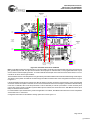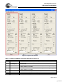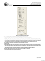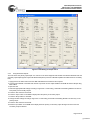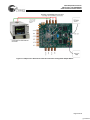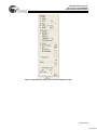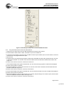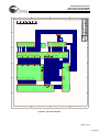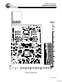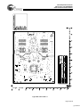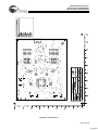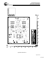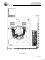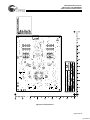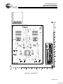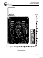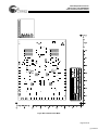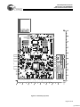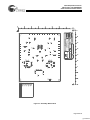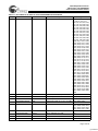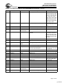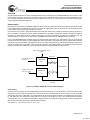
1
Quad Independent Channel HOTLink II™ CYV15G0404DXB Video PHY Demonstration Board Users Guide Cypress Semiconductor Corporation • 3901 North First Street • San Jose, CA 95134 • 408-943-2600 Revised February 2, 2005 [+] Feedback Quad Independent Channel HOTLink II™ CYV15G0404DXB Video PHY Demonstration Board TABLE OF CONTENTS 1.0 INTRODUCTION .............................................................................................................................. 5 2.0 KIT CONTENTS ............................................................................................................................... 5 3.0 DEMO BOARD FEATURES ............................................................................................................ 6 4.0 BOARD ARCHITECTURE ............................................................................................................... 7 4.1 Cable Driver and Equalizer Interfaces ........................................................................................ 7 4.2 Clocking Architecture .................................................................................................................. 8 4.3 FPGA and Control Architecture ................................................................................................ 10 4.4 Power Supply ............................................................................................................................ 11 5.0 GUI AND OPERATING MODES .................................................................................................... 12 5.1 Setting the SDI Data Rate ......................................................................................................... 14 5.2 Serial Interface I/O Selection .................................................................................................... 15 5.3 Standard ................................................................................................................................... 15 5.4 Transmit Test Pattern ............................................................................................................... 16 5.5 Status ........................................................................................................................................ 16 6.0 SAMPLE TEST PROCEDURES ....................................................................................................17 6.1 Required Equipment ................................................................................................................. 17 6.2 Tektronix WFM 700 ................................................................................................................... 17 6.3 Tests ......................................................................................................................................... 19 6.3.1 Generating SD Color Bar Patterns .................................................................................................. 19 6.3.2 Generating HD Color Bar Patterns and Reclocking the Data Three Times .................................... 20 6.3.3 Using Redundant Outputs ............................................................................................................... 22 6.3.4 Using Selectable Inputs and Automatic Rate Detection .................................................................. 25 7.0 SUMMARY ..................................................................................................................................... 29 8.0 REFERENCES ............................................................................................................................... 29 APPENDIX A: SCHEMATICS OF HOTLINK II CYV15G0404DXB VIDEO DEMO BOARD ................ 30 APPENDIX B: PCB MANUFACTURING FILES (GERBER FILES) ..................................................... 43 APPENDIX C: PCB ASSEMBLY FILES (DRILL AND ASSEMBLY) ................................................... 65 APPENDIX D: BILL OF MATERIALS (BOM) OF HOTLINK II CYV15G0404DXB VIDEO DEMO BOARD.......................................................................................................................... 69 APPENDIX E: UNPACKING HOTLINK II CYV15G0404DXB VIDEO DEMO BOARD ........................ 75 APPENDIX F: CONFIGURING THE HOTLINK II CYV15G0404DXB VIDEO DEMO BOARD FOR SD-SDI TO HD-SDI UPCONVERSION .................................................. 86 Page 2 of 92 [+] Feedback Quad Independent Channel HOTLink II™ CYV15G0404DXB Video PHY Demonstration Board LIST OF FIGURES Figure 2-1. Top View of Video Demo Board ............................................................................................ 6 Figure 4-1. Placement of Cable Drivers and Equalizers and Channel-specific LEDs ............................. 7 Figure 4-2. Placement of Clocks on the Board ........................................................................................ 9 Figure 4-3. Clock Configuration ............................................................................................................. 10 Figure 4-4. Placement of FPGA and Controls ....................................................................................... 11 Figure 4-5. Placement of Power Supply and Jumper Headers.............................................................. 12 Figure 5-1. Graphical User Interface ..................................................................................................... 13 Figure 5-2. GUI–Setting the Data Rate.................................................................................................. 15 Figure 5-3. GUI–Selecting the Serial I/Os ............................................................................................. 15 Figure 5-4. GUI–Selecting the Standards–SD....................................................................................... 15 Figure 5-5. GUI–Selecting the Standards–HD....................................................................................... 16 Figure 5-6. GUI–Selecting the Test Patterns......................................................................................... 16 Figure 5-7. GUI–Selecting Status .......................................................................................................... 17 Figure 6-1. Tektronix WFM 700–Front View .......................................................................................... 18 Figure 6-2. Tektronix WFM 700–Rear View .......................................................................................... 18 Figure 6-3. Sample Test 1–Generating and Transmitting Color Bars.................................................... 19 Figure 6-4. GUI Setting for Sample Test 1 ............................................................................................ 20 Figure 6-5. Sample Test 2–Transmits Color Bar Data Via Three Reclockers ....................................... 21 Figure 6-6. GUI Setting for Sample Test 2 ............................................................................................ 22 Figure 6-7. Sample Test 3–Generate and Transmit Color Bars Through Both Output Buffers ............. 23 Figure 6-8. GUI Setting for Sample Test 3–Transmit SD-SDI Color Bars ............................................. 24 Figure 6-9. GUI Setting for Sample Test 3–Transmit HD-SDI Color Bars ............................................. 25 Figure 6-10. Sample Test 4–Selectable Inputs and Auto Rate Detection ............................................. 26 Figure 6-11. GUI Setting for Sample Test 4: Step 6 .............................................................................. 27 Figure 6-12. GUI Settings for Sample Test 4: Step 9 ............................................................................ 28 Figure 6-13. GUI Setting for Sample Test 4: Step 13 ............................................................................ 29 Page 3 of 92 [+] Feedback Quad Independent Channel HOTLink II™ CYV15G0404DXB Video PHY Demonstration Board LIST OF TABLES Table 4-1. Interface of Cable Drivers and Equalizers to HOTLink II Serial I/Os ..................................... 8 Table 5-1. Summary of GUI Button Functionality (Shown Here for Channel A) ................................... 13 Page 4 of 92 [+] Feedback Quad Independent Channel HOTLink II™ CYV15G0404DXB Video PHY Demonstration Board 1.0 Introduction The Quad Independent Channel HOTLink II CYV15G0404DXB Video Demonstration (Demo) Board is a full-fledged serial digital video reference platform that demonstrates the HOTLink II video physical layers (PHYs) interfacing to industry-standard cable drivers and equalizers. Upstream processing of the video data is performed using on-board Altera Cyclone FPGAs. The board also has a flexible clocking architecture with automatic rate detection that allows the board to pass video traffic in multiple formats. The Independent Channel HOTLink II devices[1] are capable of simultaneously operating each channel at a different data rate. The CYV15G0404DXB has the additional capability of performing independent reclocking on a per-channel basis. The Independent Channel HOTLink II CYV15G0404DXB Video Demo Board demonstrates: • the ability of the Cypress family of transceivers to pass serial digital video at signaling rates from 270 Mb/s to 1485 Mb/s • the independent channel functionality of the applicable devices[1] • the ability to use a HOTLink II transceiver with an FPGA for auto rate detection and clock reconfiguration • the ability to perform reclocking in the HOTLink II CYV15G0404DXB device • the flexible configuration abilities of Cypress Microsystems’ PSoC microcontroller • the use of Cypress EZ-USB FX2™ USB microcontroller for video data and in-system configuration applications • on-board FPGAs that generate and receive different video test patterns. Although this board uses the CYV15G0404DXB device, the same board can be used as an evaluation vehicle for any device in the HOTLink II Independent Channel family of devices. Please refer to the data sheets for descriptions of the HOTLink II Independent Channel family of devices. 2.0 Kit Contents The kit contains the following: 1. Quad Independent Channel HOTLink II CYV15G0404DXB Video PHY Demo Board, as shown in Figure 2-1. 2. CD containing: a. Graphical User Interface (GUI) set-up file[2] b. Application Notes c. Demo board user’s guide (this document) d. Cypress’ device data sheets e. Schematics 3. 75Ω Coaxial cable 4. AC/DC wall adapter 5. USB cable 6. Dear Customer Letter 7. Kit checklist. Notes: 1. The Independent Channel HOTLink II family consists of the CYV15G0403DXB, CYV15G0404DXB, CYV15G0104TRB, CYV15G0203TB, CYV15G0204RB, CYV15G0204TRB, CYV15G0403TB, CYV15G0404RB. Refer to each data sheet for a description. 2. Please see Appendix E for instructions on installation. Page 5 of 92 [+] Feedback Quad Independent Channel HOTLink II™ CYV15G0404DXB Video PHY Demonstration Board Figure 2-1. Top View of Video Demo Board 3.0 Demo Board Features This section highlights the key features of the Quad Independent Channel HOTLink II CYV15G0404DXB Video PHY Demo Board. • Video transport at multiple rates of 270 Mb/s, 360 Mb/s, 540 Mb/s, and 1485 Mb/s • Auto-rate detection • Low-Jitter outputs • Programmable clocking options for different SMPTE data rates • SMPTE scrambler/descrambler functionality implemented in FPGA • 4x4 clock header to support multiple clocking options • High-speed USB FX2 microcontroller to configure FPGAs • Configuration of HOTLink II device using Cypress Microsystems PSoC Microcontroller • Reclocking Deserializers • 6V DC supply with on-board voltage regulator to prevent noise transfer from external power sources • Interfaces to industry-standard equalizers and cable drivers • LED status indicators • User-friendly GUI • Windows 2000/XP supported. Page 6 of 92 [+] Feedback Quad Independent Channel HOTLink II™ CYV15G0404DXB Video PHY Demonstration Board 4.0 Board Architecture The architecture of the board is shown in Figure 4-1 through Figure 4-4. The heart of the board is the Quad Independent Channel HOTLink II CYV15G0404DXB device. The device has four independent transceiver channels. Each transceiver has a transmitter with two outputs and a receiver with two selectable inputs. Each CYV15G0404DXB channel also incorporates a reclocking deserializer. Each transmitter performs 10-to-1 serialization. Each receiver includes a Clock and Data Recovery PLL (CDR PLL with embedded VCO and loop filter) and 1-to-10 deserializer. On the board, the parallel interface of the CYV15G0404DXB is connected to the on-board FPGAs (U2 and U3). All serial outputs (except OUTA2) are connected to commercially-available cable drivers. All serial inputs (excluding INA2) are connected to commercially-available equalizers. The CYV15G0404DXB is configured via an 8-bit data/4-bit address configuration interface. This configuration is controlled via a Cypress Microsystems PSoC microcontroller (U14). The architecture of the board is described in the following sections. 4.1 Cable Driver and Equalizer Interfaces The serial I/Os of the HOTLink II device are connected to various equalizers on the receive side and various cable drivers on the transmit side as shown in Figure 4-1. The different cable drivers, equalizers and their connections to the HOTLink II device are shown in Table 4-1. Note that all primary interfaces (INx1 and OUTx1) of each channel support multiformat (both HD and SD) drivers and equalizers, while the secondary interfaces (INx2 and OUTx2) support SD only. OUTA2+/- SMA (J4 and J2) (No CableDriver) INB1 (J11) (GS1524 Equalizer) INB2 (J10) OUTB1 (J9) (CLC014 (GS1528 CD) Equalizer) OUTB2 (J8) (CLC001 CD) Channel A LEDs Channel B LEDs INA2+/- SMA (J3 and J5) (No Equalizer) OUTA1 (J6) (GS1528 CD) INA1 (J7) (GS1524 Equalizer) OUTD2 (J16) (CLC007 CD) IND2 (J19) (CLC014 Equalizer) OUTD1 (J17) (GS1528 CD) IND1 (J18) (GS1524 Equalizer) OUTC2 (J12) (GS9028 CD) INC2 (J15) (GS9024 OUTC1 (J14) Equalizer) (GS1528 CD) INC1 (J13) (GS1524 Equalizer) Channel C LEDs Channel D LEDs Figure 4-1. Placement of Cable Drivers and Equalizers and Channel-specific LEDs Page 7 of 92 [+] Feedback Quad Independent Channel HOTLink II™ CYV15G0404DXB Video PHY Demonstration Board Table 4-1. Interface of Cable Drivers and Equalizers to HOTLink II Serial I/Os HOTLink II Channel Serial I/O of HOTLink II Device Interfacing Cable Driver Interfacing Equalizer Supported Standard Channel A OUTA1+ Gennum GS1528 x HD-SDI and SD-SDI Channel B Channel C Channel D 4.2 INA1+ x Gennum GS1524 OUTA2+ No Cable Driver (SMA) x INA2+ x No Equalizer (SMA) Supports any data rate from 195 Mb/s–1500 Mb/s (not SMPTE-compliant) OUTB1+ Gennum GS1528 x HD-SDI and SD-SDI INB1+ x Gennum GS1524 OUTB2+ National CLC001 x INB2+ x National CLC014 OUTC1+ Gennum GS1528 x INC1+ x Gennum GS1524 OUTC2+ Gennum GS9028 x INC2+ x Gennum GS9024 OUTD1+ Gennum GS1528 x IND1+ x Gennum GS1524 OUTD2+ National CLC007 x IND2+ x National CLC014 SD-SDI HD-SDI and SD-SDI SD-SDI HD-SDI and SD-SDI SD-SDI Clocking Architecture The board has multiple clocking options to allow for flexible testing and configuration. On each channel, the user can select either the on-board programmable clock, on-board 74.25-MHz crystal oscillator (for HD-SDI/SMPTE 292M), a clock provided by the FPGA, or an external clock. The on-board programmable clock plays a useful role in the auto rate detection mechanism, which dynamically reprograms the reference clock to the correct frequency, based on the incoming SDI data rate. When transmitting the video test patterns generated by the FPGA, either the programmable clock, external clock or on-board crystal oscillator (only for HD-SDI) should be used. Page 8 of 92 [+] Feedback Quad Independent Channel HOTLink II™ CYV15G0404DXB Video PHY Demonstration Board Programmable Clocks for Each Channel B C (U13) (U12) D A (U11) (U10) A (X5) B (X2) B (JP13) A (JP11) 74.25 MHz Crystal Oscillators Clock Config Headers for Each D (JP10) Channel C (X4) C (JP12) D (X3) Channel A 27 MHz Crystal 1 to 4 Differential Oscillator (reference for Fanout Clock programmable clocks) (X1) Buffer (U9) Channel B Channel C Channel D Figure 4-2. Placement of Clocks on the Board Note. For HD-SDI transmit jitter measurements, it is recommended to avoid using the programmable clock due to the high intrinsic jitter generated by this clock. This jitter will not influence the output jitter in reclocker mode, so the programmable clock may be used to measure reclocked jitter generation. To measure HD-SDI transmit jitter of the HOTLink II video demo board, it is recommended to use the on-board crystal oscillator. The board allows various video test patterns to be generated by the FPGA at different rates and transmitted through serial outputs. The selection of the pattern and data rate is made through the USB host interface GUI. Clock configuration instructions are given in Figure 4-3. If the programmable clock option is selected, the data rate setting in the GUI controls the output frequency of the programmable clock. If the external clock option is selected, the user must ensure that the external clock frequency matches the data rate setting in the GUI. For HD-SDI, either a full-rate (148.5 MHz or 148.5/1.001 MHz) or half-rate (74.25 MHz or 74.25/1.001 MHz) clock may be used. If the on-board 74.25-MHz crystal oscillator option is selected, the GUI must be set to 1485 Mb/s and the FR (FullRate) box should be left unchecked. For further details on jitter measurement, please see application note entitled, SDI SMPTE Jitter Performance of the Independent Channel HOTLink II Transceiver. Configuration instructions for the different clocking options are found in Figure 4-3. Page 9 of 92 [+] Feedback Quad Independent Channel HOTLink II™ CYV15G0404DXB Video PHY Demonstration Board JP10, JP11, JP12, JP13 GND 1 5 2 6 3 7 OSC+ 9 GND 13 REFCLKx+ FCLKx+ FCLKx- 10 14 CLOCKOUT+ 11 15 CLOCKOUT- REFCLKx4 8 12 16 GND GND OSC- GND Micrel Programmable Clock SY87729 GND The position of the Micrel programmable clock chip is given to set the correct orientation for determining the pin numbers for clock configuration. Note: Jumpers 6 and 10, and jumpers 7 and 11 are physically shorted for header design considerations. On board programmable clock option: Jumper 14 to 10 and Jumper 15 to 11 for using Programmable Micrel clock as Reference Clock. Remove all other jumpers from the header. This option must be chosen if the auto rate detect feature of the board is used. On board 74.25 MHz crystal oscillator clock option: Jumper 9 to 10 and Jumper 12 to 11 for using 74.25 MHz crystal oscillator clock as Reference Clock. All other jumpers must be removed. This option should be chosen for HD-SDI transmit jitter measurement. The GUI must be set to a datarate of 1485 Mb/s (FR box unchecked) for the associated channel. FPGA clock option: Jumper 2 to 6 and Jumper 3 to 7 for using FPGA clock (FCLK) as Reference Clock. Remove all other jumpers from the clock configuration header. This clock option is only used when implementing the upconversion feature of the board. See Appendix F for further details. External clock option: Remove all jumpers from the clock configuration header. Provide a differential clock to pins 6 and 7, with pins 5 and 8 as respective grounds (pins 6 and 5 and pins 7 and 8 are signal and ground pairs). Ensure that the GUI is set to the same clock frequency as the external clock. Figure 4-3. Clock Configuration 4.3 FPGA and Control Architecture The board contains two FPGAs, U2 and U3. The FPGA U2 interfaces to channels A and B of the CYV15G0404DXB device. The FPGA U3 interfaces to channels C and D of the CYV15G0404DXB device. The major functions performed by the FPGA are as follows. Page 10 of 92 [+] Feedback Quad Independent Channel HOTLink II™ CYV15G0404DXB Video PHY Demonstration Board 1. Video test pattern generation. For SD-SDI, the FPGA can generate EG1 Color Bar Data, Grey Pattern, SMPTE RP178, and SMPTE RP178 alternate SDI checkfield patterns. For HD-SDI, the FPGA can generate Color Bar Data, Grey Pattern, SMPTE RP198, and SMPTE RP198 alternate SDI checkfield patterns. 2. Auto rate detection and clock reconfiguration. The FPGA plays an important role in automatically detecting the incoming data rate and reconfiguring the programmable clock to the correct frequency. The CYV15G0404DXB configuration interface (8-bit data and 4-bit address) is configured through a Cypress Microsystems PSoC microcontroller. The PSoC receives instructions from the host PC through the on-board USB interface. The on-board USB interface is used to control the various operating modes of the device through a flexible GUI. The USB interface is also used to re-program the FPGA and the PSoC microcontroller. HOTLink II CYV15G0404DXB (U1) FPGA for channels A and B (U2) Cypress Microsystems PSoC Microcontroller (U14) Configuration Devices (U4 and U5) PSoC Programming Header for external PSoC configuration (JB5) 128-bit I2C Bus Serial EEPROM boot EEPROM for USB micro-controller (U8) USB Interface Connector (J20) Cypress FX2TM USB Microcontroller (U7) FPGA for channels C and D (U3) Processor Supervisory Circuit (U6) 24MHz crystal for USB(Y1) Figure 4-4. Placement of FPGA and Controls 4.4 Power Supply The entire board is powered through a single 6V DC power supply. The 6V input is down-converted using on-board regulators to different voltages for the various devices in the board. The kit for the board includes a compatible 6V AC wall power supply adapter. Page 11 of 92 [+] Feedback Quad Independent Channel HOTLink II™ CYV15G0404DXB Video PHY Demonstration Board Parallel Jumper Headers (JP14, JP15, JP16, JP17, JP18, JP19, JP20, JP21) HOTLink II CYV15G0404DXB (U1) A C B D D C 3-Terminal Positive Regulator (Q2) DC-DC Converter 25W 8V in, 3.3V out (U15) Channel A Channel B Channel C Channel D 6V DC 3-Terminal Positive Regulator (Q1) Power Supply Jack (J1) Figure 4-5. Placement of Power Supply and Jumper Headers 5.0 GUI and Operating Modes Please refer to Appendix E for instructions on installing the GUI on a PC/Laptop and configuring the computer to recognize the USB device. A picture of the GUI window is presented in Figure 5-1. A summary of the functionality of the buttons for channel A is presented in Table 5-1. The description of each button’s functionality applies equally to all channels. Page 12 of 92 [+] Feedback Quad Independent Channel HOTLink II™ CYV15G0404DXB Video PHY Demonstration Board Figure 5-1. Graphical User Interface Table 5-1. Summary of GUI Button Functionality (Shown Here for Channel A) Group Button Name Standard SMPTE Functionality (On Click) No action. This radio button is always selected. 1080i (see channel C in Standard for HD-SDI, automatically checked when user selects 1485Mb/s in Tx/Rx Rate the above figure) Panel of the GUI. NTSC Standard for SD-SDI. The user can check NTSC when they are transmitting/receiving data at 270 Mb/s, 360 Mb/s, or 540 Mb/s. PAL Standard for SD-SDI. The user can check PAL when they are transmitting/receiving data at 270 Mb/s, 360 Mb/s, or 540 Mb/s. Interface TxPrim Transmit data via OUTA1 (supports both SD and HD) TxSec Transmit data via OUTA2 (supports SD only) RxPrim Receive data via INA1 (supports both SD and HD) Page 13 of 92 [+] Feedback Quad Independent Channel HOTLink II™ CYV15G0404DXB Video PHY Demonstration Board Table 5-1. Summary of GUI Button Functionality (Shown Here for Channel A) (continued) Group Tx/Rx Rate Tx Source Status Button Name Receive data via INA2 (supports SD only) 270 Mb/s SD-SDI: SMPTE 259M-C 360 Mb/s SD-SDI: SMPTE 259M-D 540 Mb/s SD-SDI: SMPTE 344M 1485 Mb/s HD-SDI: SMPTE 292M Auto Rate Detect Programmable clock is reconfigured to the incoming video data rate and all other Tx/Rx Rate buttons will display which frequency the programmable clock is set to. FR Setting the source clock frequency for HD-SDI as either full-rate (148.5 MHz) or half rate (74.25 MHz). When the check-box is checked, a full-rate 148.5 MHz clock is used; when unchecked, a 74.25 MHz clock is used. EG1 Color Bars The FPGA generates EG1 color bars, which will be transmitted out on OUTA1 or OUTA2 or both. Grey The FPGA generates a uniform grey pattern, which will be transmitted out on OUTA1 or OUTA2 or both. RP178/198 The FPGA generates RP178/198 pattern (a pink half-frame on top of a grey half-frame, which will be transmitted out on OUTA1 or OUTA2 or both. RP 178/198 Alt. The FPGA generates an alternative set of the RP178/198 pattern which will be transmitted out on OUTA1 or OUTA2 or both. Reclocker Reclock the recovered data from the clock and data recovery unit and retransmit it through the serial outputs of the same channel. Up Convert Ch B Functionality not yet implemented. MCL Maximum Cable Length: for normal operation there is no need for the user to touch this (i.e. leave at 300m). If user would like to test at specific cable lengths then the bar can be set to the desired setting. Auto Rate Locked Button selected when the correct data rate is detected. CD Carrier Detect: Button selected when the amplitude of the signal on equalizer is above the MCL threshold. LFI Link Fault Indicator: Button automatically selected when HOTLink II CYV15G0404DXB does NOT receive a valid serial signal on the relevant channel. CRC Errors Cyclic Redundancy Check Errors Indicator Bar: indicator bar indicates data reception errors. CLI Cable Length Indicator: estimates length of the cable being used for transmitting/receiving data. Output from cable equalizer. Channel Run/Stop A 5.1 Functionality (On Click) RxSec Hitting run configures the channel with the applied settings; hitting stop ends operation and powers down channel A. Setting the SDI Data Rate The appropriate data rate is set by selecting the appropriate button in the Tx/Rx Rate Box of the GUI. The various data rate options are 270 Mb/s (SD-SDI/SMPTE 259M-C), 360 Mb/s (SMPTE 259M-D), 540 Mb/s (SMPTE 344M) or 1485 Mb/s (HD-SDI). See Figure 5-2 for a picture of this GUI panel. The FR (Full Rate) check box adjacent to the 1485-Mb/s option is for setting the source clock frequency for HD-SDI as either full-rate (148.5 MHz) or half-rate (74.25 MHz), via the programmable clock. When the check-box is checked, a full-rate 148.5-MHz clock is used, and when unchecked, a 74.25-MHz clock is used. This button is active only when the 1485-Mb/s button is selected. If the programmable clock option is selected, the data rate setting in the GUI controls the output frequency of the programmable clock. If the external clock option is selected, the user must ensure that the external clock frequency matches the data rate setting in the GUI. If the on-board 74.25-MHz crystal oscillator is used, the 1485 Mb/s option must be selected with the FR box left unchecked. See Section 4.2 for information on selecting clock options. Page 14 of 92 [+] Feedback Quad Independent Channel HOTLink II™ CYV15G0404DXB Video PHY Demonstration Board If the output is to be viewed on a Tektronix WFM 700 waveform monitor, the user should not select the 360 Mb/s or 540 Mb/s options because this waveform monitor does not support these data rates, and consequently, no images will be displayed on the monitor. Figure 5-2. GUI–Setting the Data Rate Auto Rate Detect When the Auto Rate Detect button is selected, the programmable clock is reconfigured to match the incoming video data rate and all other data rate buttons will be disabled. Upon clicking “Run,” various rates are attempted until a valid SMPTE data rate is detected on the input. This is shown as the last button in Figure 5-2. During the Auto Rate Detection function, a radial dot loops through each data rate as it is attempted. If the data rate is successfully detected, the dot stops next to the rate of the incoming data stream. For this feature to function, the programmable clock option must be selected. 5.2 Serial Interface I/O Selection Each HOTLink II transmit channel has redundant outputs. Either one or both outputs can be enabled to transmit the same data. When TxPrim is checked, the primary serial outputs OUTx1 are enabled. When TxSec is checked, the secondary serial outputs OUTx2 are enabled. Note that both primary and secondary outputs can be enabled simultaneously. Each HOTLink II receive channel has selectable dual inputs. Either INx1 (RxPrim) or INx2(RxSec), but not both, can be selected as the input serial data source for the respective channel. See Figure 5-3 for a picture of the GUI panel. Figure 5-3. GUI–Selecting the Serial I/Os 5.3 Standard The first box in the top of the GUI sets the video standard. For SD, the supported SMPTE formats are NTSC and PAL as shown in Figure 5-4. For HD, the supported format is 1080i and upon selecting 1485 Mb/s in the “Tx/Rx Rate” panel, the “Standard” panel will reflect the HD standard as shown in Figure 5-5. Figure 5-4. GUI–Selecting the Standards–SD Page 15 of 92 [+] Feedback Quad Independent Channel HOTLink II™ CYV15G0404DXB Video PHY Demonstration Board Figure 5-5. GUI–Selecting the Standards–HD 5.4 Transmit Test Pattern For SD-SDI, the FPGA can be configured to generate EG1 Color Bar, SMPTE RP178 SDI checkfield, SMPTE RP178 Alternate SDI checkfield, or Grey field patterns. For HD-SDI, the FPGA can be configured to generate Color Bar, SMPTE RP198 SDI checkfield, SMPTE RP198 Alternate SDI checkfield, or Grey field patterns. The Maximum Cable Length (MCL) scroll bar should be set to 300m for normal operating conditions. See Figure 5-6 for details. Reclocking Function Figure 5-6. GUI–Selecting the Test Patterns Reclocker The CYV15G0404DXB has an integrated reclocker function to reclock the recovered data from the clock and data recovery unit and retransmit it through the serial outputs of the same channel. This can be set by selecting the Reclocker button. If both Reclocker and Auto Rate Detect are selected, and the programmable clocking option is enabled, the auto rate detect logic will detect the incoming data rate and reconfigure the clocks to perform reclocking function on the selected channel. See Figure 5-6 for a picture of the reclocker radio button. 5.5 Status The status panel reflects the real time status of the board; the user has no control of this panel. The “Cable Length Indicator (CLI)” estimates the length of the cable being used between a transmitter and the receiver on that channel. The “Cyclic Redundancy Check (CRC) Errors” status bar indicates the number of errors detected after the received signal goes through the appropriate cyclic redundancy check. The “Link Fault Indicator (LFI)” is asserted when the HOTLink II CYV15G0404DXB does not receive a valid signal. The “Carrier Detect (CD)” is automatically checked when the amplitude of the incoming signal is greater than the threshold. The “Auto Rate Locked” button is selected when the data rate for incoming data is detected and the clock is programmed to the corresponding frequency. Page 16 of 92 [+] Feedback Quad Independent Channel HOTLink II™ CYV15G0404DXB Video PHY Demonstration Board Figure 5-7. GUI–Selecting Status 6.0 Sample Test Procedures Before performing the sample tests, please be sure to read Appendix E. It contains instructions on installing the GUI and configuring the hardware completely. Note: The on-board FPGAs and PSoC will be preprogrammed at the factory for testing. Therefore there should be no need to program them. Appendix E contains programming instructions should you need them. 6.1 Required Equipment • Tektronix Waveform Monitor: WFM 700 • Quad Independent Channel HOTLink II CYV15G0404DXB Video PHY Demo Board • PC/Laptop with HVDB installed • USB cable • 6V DC Power Supply • Four–six BNC cables 6.2 Tektronix WFM 700 The Tektronix WFM 700 is used in the demo tests to display the signal(s) output by the video demo board on the channel(s) specified by the user. As mentioned in previous sections, the WFM 700 does not support data rates of 360 Mb/s and 540 Mb/s. For a brief description of relevant buttons for the tests, please see Figure 6-1. The connectors used in the tests are shown in Figure 6-2. Page 17 of 92 [+] Feedback Quad Independent Channel HOTLink II™ CYV15G0404DXB Video PHY Demonstration Board STATUS - Displays video format information and CRC status. Used to see if data contains errors Touchscreen allows easy user interface PICTURE - Displays video EYE - Displays eye diagram used for jitter analysis INPUT - A or B used to choose desired input Figure 6-1. Tektronix WFM 700–Front View S e r ia l D ig ita l In te r fa c e C a r d Channel B in p u t C h a n n e l A in p u t Figure 6-2. Tektronix WFM 700–Rear View Page 18 of 92 [+] Feedback Quad Independent Channel HOTLink II™ CYV15G0404DXB Video PHY Demonstration Board 6.3 Tests This section contains step-by-step tests for fully evaluating the functionality of the board. 6.3.1 Generating SD Color Bar Patterns 1. Apply power to the board and connect the USB cable between the board and the computer. 2. Connect output OUTA1 to input A of the WFM700 using a BNC cable. 3. Open the GUI. 4. Configure channel A to generate color bars in SD format. In the “Tx/Rx Rate” panel of the GUI, click on the radio box for 270 Mb/s. In the “Tx Source” panel, select “EG1 Color Bars” to generate the color bar in SD format. See Figure 6-4 for the GUI setting for transmitting color bar at 270 Mb/s. 5. Select the programmable clocking option as shown in Figure 4-3. 6. Press the “Run” button for channel A. 7. View the picture and status displays for the signal on the WFM 700. Figure 6-3. Sample Test 1–Generating and Transmitting Color Bars Page 19 of 92 [+] Feedback Quad Independent Channel HOTLink II™ CYV15G0404DXB Video PHY Demonstration Board Figure 6-4. GUI Setting for Sample Test 1 6.3.2 Generating HD Color Bar Patterns and Reclocking the Data Three Times 1. Apply power to the board and connect the USB cable between the board and the computer. 2. Connect a BNC cable between OUTC1 and IND1, a cable between OUTD1 and INB1, a cable between OUTB1 and INA1, and a cable from OUTA1 to WFM 700. The pattern is sent from the FPGA to channel C; the data is then reclocked from channel C to channel D, then reclocked from channel D to channel B, then reclocked from channel B to channel A and then displayed on the WFM. Since HD color bars are transmitted, the primary outputs/inputs of each channel should be used. 3. For all channels, configure the clock headers to the programmable clock option. 4. Open the GUI. 5. Select appropriate buttons on the GUI according to Figure 6-6. Please note that there are two methods for setting the data rate on the reclocker channels. One method is to select “Auto Rate Detect”, which will reconfigure the programmable clocks to the incoming data rate. The other method is to set the data rate for all reclocked channels to be the same as the data rate of the transmitting channel. In the set up shown in Figure 6-5 and Figure 6-6, the transmitting data rate is 1485 Mb/s which is transmitting HD color bars. All reclocked channels are configured to automatically detect this data rate. 6. Press the “Run” button for channel C, then channel A, then channel B, then channel D. 7. View the picture display of the signal on the WFM 700. Page 20 of 92 [+] Feedback Quad Independent Channel HOTLink II™ CYV15G0404DXB Video PHY Demonstration Board Figure 6-5. Sample Test 2–Transmits Color Bar Data Via Three Reclockers Page 21 of 92 [+] Feedback Quad Independent Channel HOTLink II™ CYV15G0404DXB Video PHY Demonstration Board Figure 6-6. GUI Setting for Sample Test 2 6.3.3 Using Redundant Outputs This test shows that primary input/output of a channel on the board supports both SD-SDI and HD-SDI standards while the secondary input/output supports only the SD-SDI standard (due to presence of SD-SDI equalizers and cable drivers on secondary I/Os). 1. Apply power to the board and connect the USB cable between the board and the computer. 2. Connect output OUTB1 to the WFM 700 channel A input and connect output OUTB2 to the WFM 700 channel B input using BNC cables. 3. Open the GUI. 4. Select the appropriate GUI settings according to Figure 6-8. For this setting, channel B is transmitting SD-SDI color bars on both primary and secondary outputs. 5. Press the “Run” button for channel B. 6. Press the “Input” button on the WFM to display either the primary or secondary output. 7. Press the “Stop” button for channel B. 8. Change the GUI settings according to Figure 6-9. For this setting, channel B is transmitting HD-SDI color bars only on the primary output. 9. Press the “Run” button for channel B. 10.Press the Input button on the WFM 700 to display either the primary or secondary output. No signal is shown when the secondary output is selected. Page 22 of 92 [+] Feedback Quad Independent Channel HOTLink II™ CYV15G0404DXB Video PHY Demonstration Board Figure 6-7. Sample Test 3–Generate and Transmit Color Bars Through Both Output Buffers Page 23 of 92 [+] Feedback Quad Independent Channel HOTLink II™ CYV15G0404DXB Video PHY Demonstration Board Figure 6-8. GUI Setting for Sample Test 3–Transmit SD-SDI Color Bars Page 24 of 92 [+] Feedback Quad Independent Channel HOTLink II™ CYV15G0404DXB Video PHY Demonstration Board Figure 6-9. GUI Setting for Sample Test 3–Transmit HD-SDI Color Bars 6.3.4 Using Selectable Inputs and Automatic Rate Detection 1. Apply power to the board and connect the USB cable between the board and the computer. 2. Connect OUTB1 to IND2, OUTA1 to IND1, and OUTD1 to input A of the WFM 700. 3. Configure the clock header for channel A to the 74.25-MHz on-board crystal oscillator option, the clock header for channel B and channel D to the programmable clock option. 4. Open the GUI 5. Configure channel A to generate the grey pattern in HD format at 1485 Mb/s and channel B to generate the EG1 color bars in SD format at 270 Mb/s. For channel D, select TxPrim and RxPrim with Auto Rate Detect and Reclocker enabled. See Figure 6-11. 6. Press the “Run” button for channel A, channel B, and channel D. 7. View the picture display of the signal on the WFM 700. The user should see the grey pattern in HD-SDI format displayed. 8. Press the “Stop” button for channel D. 9. Keep the GUI settings for channel A and channel B. For channel D, select TxPrim and RxSec with Auto Rate Detect and Reclocker enabled. See Figure 6-12. 10.Press the “Run” button for channel A, channel B, and channel D. 11.View the picture display of the signal on the WFM 700. The user should see the EG1 color bars in SD-SDI format displayed. 12.Press the “Stop” button for all channels. 13.Keep the GUI settings for channel A and channel B. For channel D, keep the settings in the “Interface” panel; select the data rate to be 270 Mb/s and reclocker enabled. See Figure 6-13. 14.Press the “Run” button for channel A, channel B, and channel D. Page 25 of 92 [+] Feedback Quad Independent Channel HOTLink II™ CYV15G0404DXB Video PHY Demonstration Board 15.View the picture display of the signal on the WFM 700. The user should see the EG1 color bars in SD-SDI format displayed. 16.Press the “Stop” button for all channels. Note: For this test, the clock headers for channel A can be configured to either the on-board programmable clock option or the on-board 74.25-MHz crystal oscillator clock option. Clock headers for channel B and channel D should be configured to the onboard programmable clock option. Figure 6-10. Sample Test 4–Selectable Inputs and Auto Rate Detection Page 26 of 92 [+] Feedback Quad Independent Channel HOTLink II™ CYV15G0404DXB Video PHY Demonstration Board Figure 6-11. GUI Setting for Sample Test 4: Step 6 Page 27 of 92 [+] Feedback Quad Independent Channel HOTLink II™ CYV15G0404DXB Video PHY Demonstration Board Figure 6-12. GUI Settings for Sample Test 4: Step 9 Page 28 of 92 [+] Feedback Quad Independent Channel HOTLink II™ CYV15G0404DXB Video PHY Demonstration Board Figure 6-13. GUI Setting for Sample Test 4: Step 13 7.0 Summary The Cypress HOTLink II family of transceivers are compliant to requirements specified by SMPTE for SD-SDI and HD-SDI serial interfaces. The evaluation platform provides a full-fledged reference design that enables customers to easily implement Serial Digital Interface systems with HOTLink II Video PHYs. 8.0 References 1. Television—10-Bit 4:2:2 Component and 4fSC Composite Digital Signals–Serial Digital Interface, ANSI/SMPTE 259M–1997, Society of Motion Picture and Television Engineers, 1997. 2. Television—Component Video Signal 4:2:2 - Bit-Parallel Digital Interface, ANSI/SMPTE 125M-1995, Society of Motion Picture and Television Engineers, 1995. 3. Television—System M/NTSC Composite Video Signals–Bit-Parallel Digital Interface, ANSI/SMPTE 244M-1995, Society of Motion Picture and Television Engineers, 1995. 4. Television—Bit-Parallel Digital Interface–Component Video Signal 4:2:2 16x9 Aspect Ratio, ANSI/SMPTE 267M-1995, Society of Motion Picture and Television Engineers, 1995. 5. Pathological Conditions in Serial Digital Video Systems, SMPTE Engineering Guidelines, EG 34-1999, Society of Motion Picture and Television Engineers, 1999. 6. Serial Digital Interface Checkfield for 10-Bit 4:2:2 Component and 4fsc Composite Digital Signals, SMPTE Recommended Practices, RP 178-1996, Society of Motion Picture and Television Engineers, 1996. 7. SDI SMPTE Jitter Performance of the Independent Channel HOTLink II Transceiver, Application Note, Cypress Semiconductor Corporation 2004. Page 29 of 92 [+] Feedback Quad Independent Channel HOTLink II™ CYV15G0404DXB Video PHY Demonstration Board Appendix A: Schematics of HOTLink II CYV15G0404DXB Video Demo Board Page 30 of 92 [+] Feedback D C 1 OUTB1+ OUTB1OUTB2+ OUTB2INB1+ INB1INB2+ INB2OUTC1+ OUTC1OUTC2+ OUTC2INC1+ INC1INC2+ INC2OUTD1+ OUTD1OUTD2+ OUTD2IND1+ IND1IND2+ IND2- OUTB1+ OUTB1OUTB2+ OUTB2INB1+ INB1INB2+ INB2OUTC1+ OUTC1OUTC2+ OUTC2INC1+ INC1INC2+ INC2OUTD1+ OUTD1OUTD2+ OUTD2IND1+ IND1IND2+ IND2- SD/HDA SD/HDB SD/HDC SD/HDD CD/MUTEA CD/MUTEB CD/MUTEC CD/MUTED CD/MUTEB2 CD/MUTED2 SSI/CDC2 OUTA1+ OUTA1OUTA2+ OUTA2INA1+ INA1INA2+ INA2- Flexible Clock &Configuration Flexible Clock &Configuration.SchDoc 2 REFCLKA+ REFCLKAREFCLKB+ REFCLKBREFCLKC+ REFCLKCREFCLKD+ REFCLKDHR ESET# B CLIA CLIB CLIC CLID CLIA CLIB CLIC CLID CYV15G0403 CYV15G0403.SchDoc OUTA1+ OUTA1OUTA2+ OUTA2INA1+ INA1INA2+ INA2- 3 SCSE1 SCSE SCL SDO SDI TD3 TD4 I2SCL I2SDA TXDC[7..0] TXCTC[1..0] TXCLKOC TXCLKC TXERRC RXDC[7..0] RXSTC[2..0] RXCLKC+ RXCLKCRCLKENC LFIC TXDD[7..0] TXCTD[1..0] TXCLKOD TXCLKD TXERRD RXDD[7..0] RXSTD[2..0] RXCLKD+ RXCLKDRCLKEND LFID TXDC[7..0] TXCTC[1..0] TXCLKOC TXCLKC TXERRC RXDC[7..0] RXSTC[2..0] RXCLKC+ RXCLKCRCLKENC LFIC TXDD[7..0] TXCTD[1..0] TXCLKOD TXCLKD TXERRD RXDD[7..0] RXSTD[2..0] RXCLKD+ RXCLKDRCLKEND LFID 4 4 GPIF Interface I2CBUS RESET# Programmming Interface I2SCL I2SDA RESET# F1CONFIG_DONE F1nCONFIG F1nCE F1DATA0 F1DCLK F1nCS F1ASDI DMINUS DPLUS F2CONFIG_DONE F2nCONFIG F2nCE F2DATA0 F2DCLK F2nCS F2ASDI PA7/*FLAGD/SLCS# IFCLK CLKOUT FD[15..0] RDY[1..0] CTL[2..0] FX2 USB Microcontroller FX2 USB Microcontroller.SchDoc Power Supply Power Supply.SchDoc PRXDD[9..0] PRXCLKD PRXDD[9..0] PRXCLKD FCLKA+ FCLKAFCLKB+ FCLKBFCLKC+ FCLKCFCLKD+ FCLKD- PTXDD[9..0] PTXCLKD PRXDC[9..0] PRXCLKC PRXDC[9..0] PRXCLKC PTXDD[9..0] PTXCLKD PTXDC[9..0] PTXCLKC PRXDB[9..0] PRXCLKB PRXDB[9..0] PRXCLKB PTXDC[9..0] PTXCLKC PTXDB[9..0] PTXCLKB PRXDA[9..0] PRXCLKA PRXDA[9..0] PRXCLKA PTXDB[9..0] PTXCLKB PTXDA[9..0] PTXCLKA Parallel Interfaces Parallel Interfaces.SchDoc PTXDA[9..0] PTXCLKA SD/HDA SD/HDB SD/HDC SD/HDD CD/MUTEA CD/MUTEB CD/MUTEC CD/MUTED CD/MUTEB2 FD[15..0] CD/MUTED2 RDY[1..0] SSI/CDC2 CTL[2..0] LDTDEN ULCD ULCC ULCB ULCA IFCLK INSELD CLKOUT INSELC INSELB PA7/*FLAGD/SLCS# INSELA LPEND F1CONFIG_DONE LPENC F1nCONFIG LPENB F1nCE LPENA F1DATA0 SPDSELD F1DCLK SPDSELC F1nCS SPDSELB F1ASDI SPDSELA F2CONFIG_DONE F2nCONFIG F2nCE F2DATA0 F2DCLK F2nCS F2ASDI SCSE1 SCSE SCL SDO SDI RESET# TDO TDI TCLK TMS TMRESET# TXDA[7..0] TXCTA[1..0] TXCLKOA TXCLKA TXERRA RXDA[7..0] RXSTA[2..0] RXCLKA+ RXCLKARCLKENA LFIA TXDB[7..0] TXCTB[1..0] TXCLKOB TXCLKB TXERRB RXDB[7..0] RXSTB[2..0] RXCLKB+ RXCLKBRCLKENB LFIB FPGA FPGA.SchDoc TXDA[7..0] TXCTA[1..0] TXCLKOA TXCLKA TXERRA RXDA[7..0] RXSTA[2..0] RXCLKA+ RXCLKARCLKENA LFIA TXDB[7..0] TXCTB[1..0] TXCLKOB TXCLKB TXERRB RXDB[7..0] RXSTB[2..0] RXCLKB+ RXCLKBRCLKENB LFIB XDATA XSC LK XRES Serial IO Interface Serial IO Interface.SchDoc MCLADJA MCLADJB MCLADJC MCLADJD MCLADJA MCLADJB MCLADJC MCLADJD 3 REFCLKA+ REFCLKAREFCLKB+ REFCLKBREFCLKC+ REFCLKCREFCLKD+ REFCLKDHR ESET# SPDSELA SPDSELB SPDSELC SPDSELD LPENA LPENB LPENC LPEND INSELA INSELB INSELC INSELD ULCA ULCB ULCC ULCD LDTDEN DATA[7..0] ADDR [3.. 0] WREN TMRESET# TMS TCLK TDO TDI DATA[7..0] ADDR[3..0] WREN FCLKA+ FCLKAFCLKB+ FCLKBFCLKC+ FCLKCFCLKD+ FCLKD- 2 XR ES XSCLK XDATA A 1 5 5 4.7n C158 1M R167 S C 2 6 Revision 12 of G. Cosens LS7652 Sheet 01 Drawn By: Linear Systems Ltd. Fiducial FID6 Fiducial FID5 Fiducial FID4 Fiducial FID3 Fiducial FID2 Fiducial FID1 1PIN TP7 1PIN TP6 1PIN TP5 1PIN TP4 1PIN TP3 1PIN TP2 1PIN TP1 DrawingNumber Date: 7/6/2004 File: Top Level.SchDoc Size Cypress Molson - Top Level USB-B VBUS DD+ GND FRM1 FRM2 J20 USB Connector 1 2 3 4 5 6 6 D C B A Quad Independent Channel HOTLink II™ CYV15G0404DXB Video PHY Demonstration Board Figure A-1. Top Level Schematic Page 31 of 92 [+] Feedback D C B A C36 0.1u C37 0.1u C38 0.1u C39 0.1u 22p C42 22p C41 C40 0.1u Y1 24 MHz 1 1 2 3 4 24LC00 A0 A1 A2 Vss U8 8 7 6 5 I2SCL I2SDA Vcc WP SCL SDA +3.3V R18 2.2K +3.3V R17 2.2K +3.3V C252 0.1u 2 IFCLK DPLUS DMINUS RDY[1..0] C168 0.1u RDY[1..0] C169 0.1u DPLUS/DMINUS should have 90 ohm +/-10% differential impedance. C35 0.1u 2 RDY1 RDY0 C255 0.1u FD[15..0] C254 0.1u R195 1k FD[15..0] C253 0.1u 1 2 3 4 5 6 7 8 9 10 11 12 13 14 15 16 17 18 19 20 21 22 23 24 25 26 27 28 29 30 C257 0.1u VCC GND RDY0/*SLRD RDY1/*SLWR RDY2 RDY3 RDY4 RDY5 AVCC XTALOUT XTALIN AGND NC NC NC VCC DPUS DMINUS GND VCC GND INT4 T0 T1 T2 IFCLK RESERVED BKPT SCL SDA C256 0.1u CLKOUT C258 0.1u 3 FD15 FD14 FD13 FD12 3 FD0 FD1 FD2 FD3 1 C259 0.1u + C260 10u 2 4 1 3 5 PD0/FD8 *WAKEUP VCC RESET CTL5 GND PA7/*FLAGD/SLCS PA6/*PKTEND PA5/FIFOADR1 PA4/FIFOADR0 PA3/*WU2 PA2/*SLOE PA1/INT1 PA0/INT0 VCC GND PC7/GPIFADR7 PC6/GPIFADR6 PC5/GPIFADR5 PC4/GPIFADR4 PC3/GPIFADR3 PC2/GPIFADR2 PC1/GPIFADR1 PC0/GPIFADR0 CTL2/*FLAGC CTL1/*FLAGB CTL0/*FLAGA VCC CTL4 CTL3 80 79 78 77 76 75 74 73 72 71 70 69 68 67 66 65 64 63 62 61 60 59 58 57 56 55 54 53 52 51 4 XRES XSCLK XDATA F1CONFIG_DONE F1nCONFIG F1nCE F1DATA0 F1DCLK F1nCS F1ASDI CTL[2..0] PA7/*FLAGD/SLCS# F2CONFIG_DONE F2nCONFIG F2nCE F2DATA0 F2DCLK F2nCS F2ASDI RESET# CTL[2..0] RESET# CTL2 CTL1 CTL0 FD8 +3.3V R16 4.7K +3.3V RESET# 4 U7 CY7C68013-100AC RST MR VDD TPS3820-33 GND WDI U6 FD11 FD10 FD9 100 99 98 97 96 95 94 93 92 91 90 89 88 87 86 85 84 83 82 81 CLKOUT GND PD7/FD15 PD6/FD14 PD5/FD13 PD4/FD12 GND PE7/GPIFADR8 PE6/T2EX PE5/INT6 PE4/RXD1OUT PE3/RXD0OUT PE2/T2OUT PE1/T1OUT PE0/T0OUT VCC INT5 PD3/FD11 PD2/FD10 PD1/FD9 RD WR VCC PB0/FD0 PB1/FD1 PB2/FD2 PB3/FD3 VCC GND TXD0 RXD0 TXD1 RXD1 PB4/FD4 PB5/FD5 PB6/FD6 PB7/FD7 GND VCC GND 31 32 33 34 35 36 37 38 39 40 41 42 43 44 45 46 47 48 49 50 FD4 FD5 FD6 FD7 +3.3V B LS7652 Drawing Number 5 Date: 7/6/2004 File: FX2 USB Microcontroller.SchDoc Size 6 6 Sheet 02 Drawn By: Linear Systems Ltd. Cypress Molson - FX2 USB Microcontroller 5 12 of G. Cosens 2 Revision D C B A Quad Independent Channel HOTLink II™ CYV15G0404DXB Video PHY Demonstration Board Figure A-2. USB FX2 Microcontroller Page 32 of 92 [+] Feedback D C B A TDO TCLK TDI TMS TMRESET# TD4 1 0 R192 1 TD3 TD1 R15 1.0K R13 1.0K +3.3V R14 1.0K 2 4 6 8 10 HEADER 5X2 1 3 5 7 9 JP9 2 2 +3.3V SCSE1 TXCLKOC TXCLKOD RXDC[7..0] RXDD[7..0] RXSTC[2..0] RXSTD[2..0] RXCLKC+ RXCLKD+ RXCLKCRXCLKDCD/MUTEC CD/MUTED PTXDC[9..0] PTXDD[9..0] F2ASDI F2DCLK F2nCS LFIC LFID CD/MUTED2 SSI/CDC2 F2nCE F2nCONFIG F2CONFIG_DONE PTXCLKC PTXCLKD TXERRC TXERRD TXCLKOA TXCLKOB RXDA[7..0] RXDB[7..0] RXSTA[2..0] RXSTB[2..0] RXCLKA+ RXCLKB+ RXCLKARXCLKBCD/MUTEA CD/MUTEB PTXDA[9..0] PTXDB[9..0] F1ASDI F1DCLK F1nCS CLKOUT IFCLK LFIA LFIB SDO SCL SCSE F1nCE F1nCONFIG F1CONFIG_DONE PA7/*FLAGD/SLCS# RESET# PTXCLKA PTXCLKB TXERRA TXERRB FD[15..0] CTL[2..0] CD/MUTEB2 3 3 TD2 TXCLKOC TXDC[7..0] TXCLKOD TXDD[7..0] RXDC[7..0] TXCTC[1..0] RXDD[7..0] TXCTD[1..0] RXSTC[2..0] TXCLKC RXSTD[2..0] TXCLKD RXCLKC+ SD/HDC RXCLKD+ SD/HDD RXCLKCPRXDC[9..0] RXCLKDPRXDD[9..0] CD/MUTEC F2DATA0 CD/MUTED RCLKENC PTXDC[9..0] RCLKEND PTXDD[9..0] SPDSELC F2ASDI SPDSELD F2DCLK PRXCLKC F2nCS PRXCLKD LFIC LPENC LFID LPEND CD/MUTED2 INSELC SSI/CDC2 INSELD F2nCE ULCC F2nCONFIG ULCD F2CONFIG_DONE SDI PTXCLKC TDO PTXCLKD RDY[1..0] TXERRC FCLKC+ TXERRD FCLKCSDO FCLKD+ SCL FCLKDSCSE1 RESET# TCK TDI TMS CLKOUT IFCLK CTL[2..0] FD[15..0] PA7/*FLAGD/SLCS# FPGA2 FPGA2.SchDoc TXCLKOA TXDA[7..0] TXCLKOB TXDB[7..0] RXDA[7..0] TXCTA[1..0] RXDB[7..0] TXCTB[1..0] RXSTA[2..0] TXCLKA RXSTB[2..0] TXCLKB RXCLKA+ SD/HDA RXCLKB+ SD/HDB RXCLKAPRXDA[9..0] RXCLKBPRXDB[9..0] CD/MUTEA F1DATA0 CD/MUTEB SDI PTXDA[9..0] RCLKENA PTXDB[9..0] RCLKENB F1ASDI SPDSELA F1DCLK SPDSELB F1nCS LPENA CLKOUT LPENB IFCLK INSELA LFIA INSELB LFIB ULCA SDO ULCB SCL LDTDEN SCSE PRXCLKA F1nCE PRXCLKB F1nCONFIG RDY[1..0] F1CONFIG_DONE TDO PA7/*FLAGD/SLCS#FCLKA+ RESET# FCLKAPTXCLKA FCLKB+ PTXCLKB FCLKBTXERRA TXERRB FD[15..0] CTL[2..0] CD/MUTEB2 TCK TDI TMS FPGA1 FPGA1.SchDoc 4 4 FCLKC+ FCLKCFCLKD+ FCLKD- TXDC[7..0] TXDD[7..0] TXCTC[1..0] TXCTD[1..0] TXCLKC TXCLKD SD/HDC SD/HDD PRXDC[9..0] PRXDD[9..0] F2DATA0 RCLKENC RCLKEND SPDSELC SPDSELD PRXCLKC PRXCLKD LPENC LPEND INSELC INSELD ULCC ULCD FCLKA+ FCLKAFCLKB+ FCLKB- TXDA[7..0] TXDB[7..0] TXCTA[1..0] TXCTB[1..0] TXCLKA TXCLKB SD/HDA SD/HDB PRXDA[9..0] PRXDB[9..0] F1DATA0 SDI RCLKENA RCLKENB SPDSELA SPDSELB LPENA LPENB INSELA INSELB ULCA ULCB LDTDEN PRXCLKA PRXCLKB RDY[1..0] B 5 Date: 7/6/2004 File: FPGA.SchDoc Size 6 2 6 Revision LS7652 of 12 G. Cosens Drawing Number Sheet 03 Drawn By: Linear Systems Ltd. Cypress Molson - FPGA's 5 D C B A Quad Independent Channel HOTLink II™ CYV15G0404DXB Video PHY Demonstration Board Figure A-3. FPGA Top Level Page 33 of 92 [+] Feedback D C B A C147 1n 0 FD[15..0] RESET# RXCLKA+ TXCLKOA RXCLKASDI SDO SCSE LFIA INSELB LPENB SCL FD[15..0] CTL[2..0] 1 CLKOUT PA7/*FLAGD/SLCS# TXDA[7..0] TXCTA[1..0] R213 FCLKA+ FCLKA- CTL[2..0] C146 0.1u +1.5VA TXCLKA TXDA[7..0] TXCTA[1..0] C3 C2 D3 D2 D4 D1 E3 E2 F1 E4 E5 F2 F3 F4 F5 G1 G2 F6 F7 G3 G4 G5 G6 H1 H2 H3 H4 H5 H6 J1 H7 J2 J5 J3 J4 K1 J6 K2 J7 K3 K7 L1 K6 K4 K5 L7 L6 L2 L3 L5 L4 M1 M3 M2 M5 M4 N1 N2 M6 N7 N5 N6 N3 N4 P5 P2 P3 R1 P4 R2 R3 T2 T3 + +3.3V F1CONFIG_DONE F1nCONFIG F1nCE F1DATA0 F1DCLK F1nCS F1ASDI FD4 FD14 FD15 FD12 FD13 FD5 FD11 FD10 FD8 FD7 FD6 CTL1 FD9 CTL0 CTL2 F1DCLK F1ASDI F1nCE RXCLKA+ TXCLKOA F1nCS F1DATA0 F1nCONFIG RXCLKA- RXDA7 TXCTA1 TXCLKA RXSTB2 TXDA1 RXDA3 C250 10u C155 0.1u +3.3V C170 0.1u +3.3V F1CONFIG_DONE F1nCONFIG F1nCE F1DATA0 F1DCLK F1nCS F1ASDI BANK1 EP1C20F324C8 rxstb[2] txda[1] rxda[3] lpenb scl txclka inselb txcta[1] RESERVED_INPUT rxda[7] RESERVED_INPUT sdo scse lfia RESERVED_INPUT RESERVED_INPUT RESERVED_INPUT RESERVED_INPUT RESERVED_INPUT RESERVED_INPUT RESERVED_INPUT RESERVED_INPUT RESERVED_INPUT RESERVED_INPUT RESERVED_INPUT rxclka_n sdi RESERVED_INPUT RESERVED_INPUT RESERVED_INPUT DATA0 nCONFIG VCCA_PLL1 rxclka_p txclkoa GNDA_PLL1 GNDG_PLL1 nCEO nCE MSEL0 MSEL1 DCLK RESERVED_INPUT fclka_p fclka_n RESERVED_INPUT RESERVED_INPUT ctl[2] reset_n RESERVED_INPUT pa7_flagd_slcs ctl[1] fd[9] ctl[0] RESERVED_INPUT fd[8] fd[7] fd[6] RESERVED_INPUT RESERVED_INPUT RESERVED_INPUT RESERVED_INPUT fd[11] fd[10] RESERVED_INPUT fd[12] fd[13] fd[5] RESERVED_INPUT fd[4] fd[14] fd[15] clkout U2A C143 0.1u C171 0.1u C20 0.1u C172 0.1u 2 C21 0.1u C173 0.1u RXDA[7..0] RXSTA[2..0] TXCTB[1..0] TXDB[7..0] TXCLKB RXDB[7..0] RXSTB[2..0] 2 INSELA TXERRA LFIB RXDA[7..0] RXSTA[2..0] TXCTB[1..0] TXDB[7..0] +3.3V 0 LPENA RCLKENA RXDB[7..0] TXERRB RXSTB[2..0] R214 POWER/GND V5 V14 P8 P11 C10 0.1u C174 0.1u VC CIO4 VC CIO4 VC CIO4 VC CIO4 +1.5V P18 M12 H12 E18 VC CIO3 VC CIO3 VC CIO3 VC CIO3 RXDA6 RXDB3 RXDA5 TXDA2 RXDB6 RXDA4 TXDA3 RXDB7 TXDA0 TXDA5 TXDA6 RXDA1 TXCTA0 TXCTB0 RXDA0 RXDB2 TXDA7 TXDA4 RXSTA0 RXDA2 TXDB1 TXDB5 RXDB1 RXSTA2 RXDB0 TXDB7 TXDB4 RXDB5 RXSTA1 TXDB0 TXCTB1 TXDB2 TXCLKB TXDB3 RXDB4 RXSTB0 SPDSELB' RXSTB1 E9 E12 A5 A14 VC CIO2 VC CIO2 VC CIO2 VC CIO2 C16 B16 G11 F11 B15 A15 C15 D14 B14 C14 E13 G10 F10 B13 A13 D13 C13 D12 C12 B12 A12 C11 D11 B11 A11 E11 C10 D10 B10 A10 E10 G9 F9 D9 C9 A9 B9 D8 C8 A8 B8 E8 E7 A7 B7 D7 C7 E6 D6 B6 C6 A6 B5 C5 D5 A4 B4 F8 G8 B3 C4 P1 M7 G7 E1 VC CIO1 VC CIO1 VC CIO1 VC CIO1 BANK2 EP1C20F324C8 rxstb[1] txerrb VCCINT GND rxstb[0] spdselb lpena rclkena txdb[3] rxdb[4] RESERVED_INPUT GND VCCINT txdb[2] txclkb insela rxdb[1] rxsta[2] rxdb[0] txdb[7] txdb[4] rxdb[5] rxsta[1] txdb[0] txctb[1] RESERVED_INPUT RESERVED_INPUT rxda[2] txdb[1] txdb[5] RESERVED_INPUT VCCINT GND rxsta[0] RESERVED_INPUT txcta[0] txctb[0] rxda[0] rxdb[2] txda[7] txda[4] RESERVED_INPUT RESERVED_INPUT txda[5] txda[6] rxda[1] lfib RESERVED_INPUT rxda[4] txda[3] rxdb[7] txda[0] RESERVED_INPUT rxdb[3] rxda[5] txda[2] rxdb[6] VCCINT GND txerra rxda[6] U2B 3 C11 0.1u C175 0.1u C12 0.1u C176 0.1u C13 0.1u C177 0.1u C14 0.1u +1.5V C178 0.1u +1.5V C15 0.1u C179 0.1u 3 C16 0.1u C180 0.1u C148 0.1u +1.5VA C17 0.1u C181 0.1u C18 0.1u C182 0.1u C19 0.1u C183 0.1u C149 1n FCLKB+ FCLKB- 221 +3.3V R196 U2E EP1C20F324C8 +1.5V V2 V17 U18 U1 L9 K10 J9 H10 B18 B1 A2 A17 VC CINT VC CINT VC CINT VC CINT VC CINT VC CINT VC CINT VC CINT VC CINT VC CINT VC CINT VC CINT GND GND GND GND GND GND GND GND GND GND GND GND GND GND GND GND GND GND GND GND GND GND GND GND GND GND GND GND V3 V18 V16 V1 U2 U17 T18 T1 L8 L11 L10 K9 K8 K11 J8 J11 J10 H9 H8 H11 C18 C1 B2 B17 A3 A18 A16 A1 1 C9 0.1u +3.3V ULCB LDTDEN RCLKENB ULCA CD/MUTEB2 CD/MUTEB SD/HDB CD/MUTEA SD/HDA +3.3V RXCLKB- TDI L7425A L270A L540A L360A LFIA CDA L7425B L540B LFIB L270B L360B CDB PTXDA1 PTXDA0 8 7 3 4 EPCS4SI8N VCC VCC VCC GND U4 TXDB6 SPDSELA' RXCLKB- TXCLKOB RXCLKB+ F1CONFIG_DONE F1nSTATUS TXCLKOB RXCLKB+ TCK TMS TDO PTXCLKA PRXCLKB LED2 D30 4 2 6 1 5 BANK3 EP1C20F324C8 F1DATA0 F1DCLK F1nCS F1ASDI led2 ledcdb ptxda[1] ptxda[0] prxclkb ledlfib led270b led360b RESERVED_INPUT RESERVED_INPUT RESERVED_INPUT led540b ptxclka RESERVED_INPUT RESERVED_INPUT led7425b RESERVED_INPUT ledlfia ledcda RESERVED_INPUT RESERVED_INPUT led270a led540a led360a RESERVED_INPUT RESERVED_INPUT led7425a RESERVED_INPUT RESERVED_INPUT fclkb_p fclkb_n CONF_DONE nSTATUS TCK TMS TDO GNDG_PLL2 GNDA_PLL2 txclkob rxclkb_p VCCA_PLL2 TDI RESERVED_INPUT RESERVED_INPUT RESERVED_INPUT RESERVED_INPUT rxclkb_n RESERVED_INPUT RESERVED_INPUT cd_mutea sd_hda RESERVED_INPUT RESERVED_INPUT RESERVED_INPUT RESERVED_INPUT RESERVED_INPUT RESERVED_INPUT RESERVED_INPUT cd_muteb sd_hdb RESERVED_INPUT RESERVED_INPUT cd_muteb2 RESERVED_INPUT RESERVED_INPUT rclkenb ulca spdsela RESERVED_INPUT ldtden RESERVED_INPUT txdb[6] ulcb U2C DATA DCLK nCS ASDI T16 T17 R17 R18 R15 R16 P16 P17 P15 P14 N14 N18 N17 N13 N12 N16 N15 M18 M17 M14 M15 M16 L18 L17 M13 L13 L16 L15 L14 K16 K15 K17 L12 K18 K14 K13 J18 K12 J16 J15 J12 J17 J14 J13 H13 H14 H15 H16 H17 H18 G18 G17 G13 G14 G15 G16 G12 F12 F18 F17 F13 F14 F16 F15 E17 E16 E15 D18 E14 D16 D15 C17 D17 4 F1DCLK F1CONFIG_DONE F1nCONFIG F1DATA0 F1ASDI PRXDB[9..0] PTXDB[9..0] PRXDA[9..0] PTXDA[9..0] RDY[1..0] 2 4 6 8 10 HEADER 5X2 1 3 5 7 9 JP6 PRXDB[9..0] PTXDB[9..0] PRXDA[9..0] PTXDA[9..0] RDY[1..0] F1nCE F1nCS +3.3V PRXCLKA PTXCLKB IFCLK 5 +1.5V 5 U3 V4 M8 N8 T4 U4 T5 U5 R4 R5 V6 U6 P6 P7 T6 R6 U7 V7 T7 R7 U8 V8 T8 R8 U9 V9 R9 T9 M9 N9 P9 U10 V10 T10 R10 P10 R11 T11 U11 V11 V12 U12 T12 R12 V13 U13 T13 R13 N10 M10 P12 P13 U14 T14 R14 V15 U15 N11 M11 U16 T15 F1nCE F1nCONFIG F1nSTATUS F1CONFIG_DONE PRXDA1 PTXDB0 PRXDB0 PTXDA2 PRXDA0 PRXDB3 PTXDB3 PRXDA4 PTXDA5 PTXDA4 PRXDA3 PTXDB2 PRXDB2 PTXDA3 PRXDA2 PTXDB1 PRXDB1 PRXDA5 PTXDA6 PTXDB4 PRXDB4 PTXDB8 PRXDB8 PRXDA8 PTXDA9 PTXDB7 PRXDB7 PRXDA7 PTXDA8 PTXDB6 PRXDB6 PRXDA6 PTXDA7 PRXDB5 PTXDB5 FD3 PTXDB9 PRXDA9 RDY0 PRXDB9 FD0 FD1 RDY1 FD2 +3.3V 0 B Date: 7/6/2004 File: FPGA1.SchDoc Size +3.3V +3.3V 3 2 1 3 2 1 3PIN JB2 3PIN JB1 L7425B L540B L360B L270B CDB LFIB L7425A L540A L360A L270A CDA LFIA SPDSELB SPDSELA 221 R179 221 R178 221 R177 221 R176 221 R175 221 R174 221 R173 221 R172 221 R171 221 R170 221 R169 221 R168 2 6 Revision 12 of G. Cosens LS7652 LED2 D14 LED2 D13 LED2 D12 LED2 D11 LED2 D10 LED2 D9 LED2 D8 LED2 D7 LED2 D6 LED2 D5 LED2 D4 LED2 D3 DrawingNumber Sheet 04 Drawn By: Linear Systems Ltd. R2 0 R1 Cypress Molson - FPGA1 10K R6 10K R5 10K R4 10K R3 SPDSELB' SPDSELA' BANK4 EP1C20F324C8 rdy[1] fd[2] VCCINT GND ifclk fd[3] ptxdb[9] prxda[9] rdy[0] prxdb[9] fd[0] fd[1] RESERVED_INPUT RESERVED_INPUT ptxdb[8] prxdb[8] prxda[8] ptxda[9] ptxdb[7] prxdb[7] prxda[7] ptxda[8] ptxdb[6] prxdb[6] prxda[6] ptxda[7] prxdb[5] ptxdb[5] GND VCCINT RESERVED_INPUT prxda[5] ptxda[6] ptxdb[4] prxdb[4] RESERVED_INPUT prxdb[3] ptxdb[3] prxda[4] ptxda[5] ptxda[4] prxda[3] ptxdb[2] prxdb[2] ptxda[3] prxda[2] ptxdb[1] prxdb[1] GND VCCINT RESERVED_INPUT RESERVED_INPUT prxda[1] ptxdb[0] prxdb[0] ptxda[2] prxda[0] VCCINT GND prxclka ptxclkb U2D 6 D C B A Quad Independent Channel HOTLink II™ CYV15G0404DXB Video PHY Demonstration Board Figure A-4. FPGA for Channel A and B Page 34 of 92 [+] Feedback D C B A RXDD[7..0] RXSTD[2..0] SCL SDO SDI SCSE1 RXCLKD+ TXCLKOD 1 RXDD[7..0] TXERRD RXSTD[2..0] 1n FCLKD+ FCLKD- C151 0.1u RXCLKD- PA7/*FLAGD/SLCS# RESET# CTL[2..0] C150 +1.5VA CTL[2..0] FD[15..0] FD[15..0] C3 C2 D3 D2 D4 D1 E3 E2 F1 E4 E5 F2 F3 F4 F5 G1 G2 F6 F7 G3 G4 G5 G6 H1 H2 H3 H4 H5 H6 J1 H7 J2 J5 J3 J4 K1 J6 K2 J7 K3 K7 L1 K6 K4 K5 L7 L6 L2 L3 L5 L4 M1 M3 M2 M5 M4 N1 N2 M6 N7 N5 N6 N3 N4 P5 P2 P3 R1 P4 R2 R3 T2 T3 + C251 10u C157 0.1u 0.1u 0.1u C185 C156 +3.3V 0.1u C184 +3.3V F2CONFIG_DONE F2nCONFIG F2nCE F2DATA0 F2DCLK F2nCS F2ASDI EP1C20F324C8 BANK1 fd[1] fd[2] fd[3] fd[13] rdy[1] fd[12] fd[4] fd[5] fd[10] RESERVED_INPUT RESERVED_INPUT fd[11] fd[6] fd[7] RESERVED_INPUT fd[8] fd[9] RESERVED_INPUT RESERVED_INPUT ctl[0] ctl[1] RESERVED_INPUT RESERVED_INPUT pa7_flagd_slcs reset_n ctl[2] rxclkd_n RESERVED_INPUT RESERVED_INPUT RESERVED_INPUT DATA0 nCONFIG VCCA_PLL1 rxclkd_p txclkod GNDA_PLL1 GNDG_PLL1 nCEO nCE MSEL0 MSEL1 DCLK RESERVED_INPUT fclkd_p fclkd_n RESERVED_INPUT RESERVED_INPUT sdi scse1 RESERVED_INPUT RESERVED_INPUT sdo RESERVED_INPUT scl RESERVED_INPUT RESERVED_INPUT RESERVED_INPUT RESERVED_INPUT RESERVED_INPUT RESERVED_INPUT RESERVED_INPUT RESERVED_INPUT RESERVED_INPUT RESERVED_INPUT RESERVED_INPUT RESERVED_INPUT rxstd[2] txerrd rxstc[2] rxdd[1] rxstc[1] txctd[1] rxstd[0] U3A +3.3V F2CONFIG_DONE F2nCONFIG F2nCE F2DATA0 F2DCLK F2nCS F2ASDI RXSTC2 RXDD1 RXSTC1 TXCTD1 RXSTD0 RXSTD2 F2DCLK F2ASDI F2nCE RXCLKD+ TXCLKOD F2nCS F2DATA0 F2nCONFIG CTL2 RXCLKD- CTL0 CTL1 FD8 FD9 FD11 FD6 FD7 FD1 FD2 FD3 FD13 RDY1 FD12 FD4 FD5 FD10 2 +3.3V RDY[1..0] PRXDD[9..0] PTXDD[9..0] PRXDC[9..0] PTXDC[9..0] 0.1u C33 0.1u C186 POWER/GND 2 0.1u C34 0.1u C187 PTXCLKC IFCLK PTXCLKD PRXCLKD CLKOUT PRXCLKC PRXDD[9..0] PTXDD[9..0] PRXDC[9..0] PTXDC[9..0] RDY[1..0] V5 V14 P8 P11 VC CIO4 VC CIO4 VC CIO4 VC CIO4 P18 M12 H12 E18 VC CIO3 VC CIO3 VC CIO3 VC CIO3 +1.5V E9 E12 A5 A14 VC CIO2 VC CIO2 VC CIO2 VC CIO2 FD0 RDY0 FD15 FD14 PTXDD0 PRXDD0 PRXDD1 PTXDD1 PTXDC0 PRXDD3 PTXDD3 PTXDC2 PRXDC1 PRXDD2 PTXDD2 PTXDC1 PRXDC0 PTXDD4 PRXDD4 PRXDC2 PTXDC3 PRXDC5 PTXDC6 PRXDD7 PTXDD7 PRXDD6 PTXDD6 PRXDC4 PTXDC5 PTXDD5 PRXDD5 PRXDC3 PTXDC4 PRXDC7 PTXDC7 PTXDD9 PRXDD8 PRXDC6 PTXDD8 PRXDC9 PRXDC8 P1 M7 G7 E1 VC CIO1 VC CIO1 VC CIO1 VC CIO1 C16 B16 G11 F11 B15 A15 C15 D14 B14 C14 E13 G10 F10 B13 A13 D13 C13 D12 C12 B12 A12 C11 D11 B11 A11 E11 C10 D10 B10 A10 E10 G9 F9 D9 C9 A9 B9 D8 C8 A8 B8 E8 E7 A7 B7 D7 C7 E6 D6 B6 C6 A6 B5 C5 D5 A4 B4 F8 G8 B3 C4 0.1u C23 0.1u C188 0.1u C24 0.1u C189 0.1u C25 0.1u C190 0.1u C26 0.1u C191 0.1u C27 +1.5V 0.1u 0.1u C28 0.1u C193 3 0.1u C29 0.1u C194 0.1u C30 0.1u 0.1u C31 0.1u C196 1n 0.1u C32 0.1u C197 221 +3.3V R197 C153 0.1u FCLKC+ FCLKC- C152 +1.5VA C195 U3E EP1C20F324C8 +1.5V EP1C20F324C8 BANK2 C192 +1.5V 3 prxdc[9] prxdc[8] VCCINT GND prxdc[7] ptxdc[7] ptxdd[9] prxdd[8] prxdc[6] ptxdd[8] RESERVED_INPUT GND VCCINT prxdc[5] ptxdc[6] prxdd[7] ptxdd[7] prxdd[6] ptxdd[6] prxdc[4] ptxdc[5] ptxdd[5] prxdd[5] prxdc[3] ptxdc[4] RESERVED_INPUT ptxdd[4] prxdd[4] prxdc[2] ptxdc[3] RESERVED_INPUT VCCINT GND prxdd[3] ptxdd[3] ptxdc[2] prxdc[1] prxdd[2] ptxdd[2] ptxdc[1] prxdc[0] RESERVED_INPUT RESERVED_INPUT ptxdc[0] prxclkc prxdd[1] ptxdd[1] RESERVED_INPUT prxdd[0] clkout ptxdd[0] ptxclkc ifclk ptxclkd prxclkd fd[15] fd[14] VCCINT GND fd[0] rdy[0] U3B V2 V17 U18 U1 L9 K10 J9 H10 B18 B1 A2 A17 VC CINT VC CINT VC CINT VC CINT VC CINT VC CINT VC CINT VC CINT VC CINT VC CINT VC CINT VC CINT GND GND GND GND GND GND GND GND GND GND GND GND GND GND GND GND GND GND GND GND GND GND GND GND GND GND GND GND V3 V18 V16 V1 U2 U17 T18 T1 L8 L11 L10 K9 K8 K11 J8 J11 J10 H9 H8 H11 C18 C1 B2 B17 A3 A18 A16 A1 1 0.1u C22 +3.3V TXDC4 TXDC0 SPDSELD' 8 7 3 4 EPCS4SI8N VCC VCC VCC GND U5 PTXDC8 CDD PRXDD9 PTXDC9 L270D LFID L7425D L540D L360D L270C L7425C L360C L540C LFIC CDC RXCLKC- TXCLKOC RXCLKC+ F2CONFIG_DONE F2nSTATUS +3.3V LED2 D31 TDI RXCLKC- TXCLKOC RXCLKC+ TCK TMS TDO CD/MUTED2 SD/HDD CD/MUTED SSI/CDC2 SD/HDC CD/MUTEC INSELC ULCC LPEND ULCD INSELD DATA DCLK nCS ASDI T16 T17 R17 R18 R15 R16 P16 P17 P15 P14 N14 N18 N17 N13 N12 N16 N15 M18 M17 M14 M15 M16 L18 L17 M13 L13 L16 L15 L14 K16 K15 K17 L12 K18 K14 K13 J18 K12 J16 J15 J12 J17 J14 J13 H13 H14 H15 H16 H17 H18 G18 G17 G13 G14 G15 G16 G12 F12 F18 F17 F13 F14 F16 F15 E17 E16 E15 D18 E14 D16 D15 C17 D17 4 4 2 6 1 5 F2DATA0 F2DCLK F2nCS F2ASDI EP1C20F324C8 BANK3 inseld txdc[4] ulcd spdseld RESERVED_INPUT ulcc lpend txdc[0] inselc RESERVED_INPUT RESERVED_INPUT sd_hdc cd_mutec RESERVED_INPUT RESERVED_INPUT RESERVED_INPUT RESERVED_INPUT cd_muted ssi_cdc2 RESERVED_INPUT RESERVED_INPUT RESERVED_INPUT cd_muted2 sd_hdd RESERVED_INPUT RESERVED_INPUT RESERVED_INPUT RESERVED_INPUT RESERVED_INPUT fclkc_p fclkc_n CONF_DONE nSTATUS TCK TMS TDO GNDG_PLL2 GNDA_PLL2 txclkoc rxclkc_p VCCA_PLL2 TDI rxclkc_n RESERVED_INPUT RESERVED_INPUT RESERVED_INPUT RESERVED_INPUT led7425c led360c led540c ledlfic ledcdc RESERVED_INPUT RESERVED_INPUT RESERVED_INPUT led270c RESERVED_INPUT RESERVED_INPUT led540d led360d RESERVED_INPUT RESERVED_INPUT led7425d RESERVED_INPUT led270d ledlfid RESERVED_INPUT ptxdc[9] RESERVED_INPUT ledcdd prxdd[9] led2 ptxdc[8] U3C F2DCLK F2CONFIG_DONE F2nCONFIG F2DATA0 F2ASDI TXCTC[1..0] TXDC[7..0] RXSTC[2..0] RXDC[7..0] TXCTD[1..0] TXDD[7..0] 2 4 6 8 10 HEADER 5X2 1 3 5 7 9 JP8 TXCTC[1..0] TXCLKC TXDC[7..0] RXSTC[2..0] RXDC[7..0] TXCTD[1..0] TXDD[7..0] TXCLKD +1.5V F2nCE F2nCS +3.3V LPENC RCLKEND LFID LFIC 0 R215 RCLKENC TXERRC 0 R216 5 5 U3 V4 M8 N8 T4 U4 T5 U5 R4 R5 V6 U6 P6 P7 T6 R6 U7 V7 T7 R7 U8 V8 T8 R8 U9 V9 R9 T9 M9 N9 P9 U10 V10 T10 R10 P10 R11 T11 U11 V11 V12 U12 T12 R12 V13 U13 T13 R13 N10 M10 P12 P13 U14 T14 R14 V15 U15 N11 M11 U16 T15 F2nCE F2nCONFIG F2nSTATUS F2CONFIG_DONE SPDSELC' TXDC7 RXDC6 SPDSELC' TXDC1 TXCTC0 TXDC3 TXDC2 RXDD6 RXDC2 TXDC5 TXCTC1 RXDD7 RXDC7 RXDD2 TXDC6 TXCLKC RXDD3 RXDC3 RXDD4 TXDD2 RXDC4 RXDC5 TXDD0 TXDD1 RXDD5 RXSTC0 TXDD3 TXDD4 RXDC1 TXDD6 TXDD5 RXDC0 RXDD0 RXSTD1 TXDD7 TXCTD0 TXCLKD 10K 10K R12 10K R11 10K R10 R9 3 2 1 3PIN JB3 +3.3V B Date: 7/6/2004 File: FPGA2.SchDoc Size 0 R8 SPDSELC L7425D L540D L360D L270D CDD LFID L7425C L540C L360C L270C CDC LFIC +3.3V LS7652 DrawingNumber 3 2 1 3PIN JB4 221 R191 221 R190 221 R189 221 R188 221 R187 221 R186 221 R185 221 R184 221 R183 221 R182 221 R181 221 R180 6 Sheet 05 Drawn By: Linear Systems Ltd. SPDSELD' +3.3V Cypress Molson - FPGA2 0 R7 EP1C20F324C8 BANK4 txctd[0] txclkd VCCINT GND rxdc[0] rxdd[0] rxstd[1] txdd[7] RESERVED_INPUT rxdc[1] txdd[6] txdd[5] RESERVED_INPUT RESERVED_INPUT rxdd[5] rxstc[0] txdd[3] txdd[4] RESERVED_INPUT rxdc[5] txdd[0] txdd[1] RESERVED_INPUT rxdc[4] txerrc txdd[2] rclkenc rxdd[4] GND VCCINT RESERVED_INPUT txdc[6] txclkc rxdd[3] rxdc[3] RESERVED_INPUT lfic rxdd[2] RESERVED_INPUT txctc[0] txdc[3] txdc[2] rxdd[6] rxdc[2] txdc[5] txctc[1] rxdd[7] rxdc[7] GND VCCINT RESERVED_INPUT RESERVED_INPUT txdc[1] lfid rxdc[6] spdselc rclkend VCCINT GND txdc[7] lpenc U3D 6 12 of G. Cosens 2 Revision SPDSELD LED2 LED2 D26 LED2 D25 LED2 D24 LED2 D23 LED2 D22 LED2 D21 LED2 D20 LED2 D19 LED2 D18 LED2 D17 LED2 D16 D15 D C B A Quad Independent Channel HOTLink II™ CYV15G0404DXB Video PHY Demonstration Board Figure A-5. FPGA for Channel C and D Page 35 of 92 [+] Feedback D C B A 1 1 2 4 6 8 10 12 14 16 18 20 22 2 PTXDC[9..0] PTXDB[9..0] PTXDC[9..0] PTXDB[9..0] PTXDA[9..0] PRXDC[9..0] PRXDB[9..0] PRXDA[9..0] PRXDC[9..0] PRXDB[9..0] PRXDA[9..0] 2 4 6 8 10 12 14 16 18 20 22 HEADER 11X2 1 3 5 7 9 11 13 15 17 19 21 JP20 HEADER 11X2 2 4 6 8 10 12 14 16 18 20 22 PTXCLKD PTXDD0 PTXDD1 PTXDD2 PTXDD3 PTXDD4 PTXDD5 PTXDD6 PTXDD7 PTXDD8 PTXDD9 PTXDD[9..0] PTXDD[9..0] 3 PRXDD[9..0] PRXDD[9..0] PRXDD0 PRXDD1 PRXDD2 PRXDD3 PRXDD4 PRXDD5 PRXDD6 PRXDD7 PRXDD8 PRXDD9 PRXCLKC PRXCLKB PRXCLKA PRXCLKD PRXDC0 PRXDC1 PRXDC2 PRXDC3 PRXDC4 PRXDC5 PRXDC6 PRXDC7 PRXDC8 PRXDC9 PRXDB0 PRXDB1 PRXDB2 PRXDB3 PRXDB4 PRXDB5 PRXDB6 PRXDB7 PRXDB8 PRXDB9 PRXDA0 PRXDA1 PRXDA2 PRXDA3 PRXDA4 PRXDA5 PRXDA6 PRXDA7 PRXDA8 PRXDA9 4 JP21 2 4 6 8 10 12 14 16 18 20 22 1 3 5 7 9 11 13 15 17 19 21 JP17 2 4 6 8 10 12 14 16 18 20 22 HEADER 11X2 1 3 5 7 9 11 13 15 17 19 21 JP15 2 4 6 8 10 12 14 16 18 20 22 HEADER 11X2 1 3 5 7 9 11 13 15 17 19 21 2 4 6 8 10 12 14 16 18 20 22 HEADER 11X2 1 3 5 7 9 11 13 15 17 19 21 JP19 1 3 5 7 9 11 13 15 17 19 21 PTXDC0 PTXDC1 PTXDC2 PTXDC3 PTXDC4 PTXDC5 PTXDC6 PTXDC7 PTXDC8 PTXDC9 PTXDB0 PTXDB1 PTXDB2 PTXDB3 PTXDB4 PTXDB5 PTXDB6 PTXDB7 PTXDB8 PTXDB9 PTXDA[9..0] JP18 PTXCLKC PTXCLKB PTXDA0 PTXDA1 PTXDA2 PTXDA3 PTXDA4 PTXDA5 PTXDA6 PTXDA7 PTXDA8 PTXDA9 4 HEADER 11X2 2 4 6 8 10 12 14 16 18 20 22 PTXCLKA 3 HEADER 11X2 1 3 5 7 9 11 13 15 17 19 21 JP16 HEADER 11X2 1 3 5 7 9 11 13 15 17 19 21 JP14 2 B 2 5 6 Revision LS7652 12 of G. Cosens Drawing Number Date: 7/6/2004 File: Parallel Interfaces.SchDoc Size 6 Sheet 06 Drawn By: Linear Systems Ltd. Cypress Molson - Parallel Interfaces 5 D C B A Quad Independent Channel HOTLink II™ CYV15G0404DXB Video PHY Demonstration Board Figure A-6. Parallel Interface Headers Page 36 of 92 [+] Feedback D C B C279 0.1u +3.3V C281 0.1u +3.3V C278 0.1u +3.3V C280 0.1u +3.3V OUT OUT X1 27 MHz +3.3V 14 VC C GND 7 C283 0.1u C285 0.1u C282 0.1u C284 0.1u 1 8 1 2 1 2 1 2 1 2 C248 0.1u +3.3V 1 NC NC NC NC NC NC NC NC i 50 ohm OUT OUT X3 74.25 MHz OUT OUT X4 74.25 MHz OUT OUT X2 74.25 MHz OUT OUT X5 74.25 MHz i 50 ohm C249 0.1u 6 4 5 4 5 4 5 4 5 R224 130 R228 130 R220 130 R232 130 C140 0.1u +3.3V 1 2 3 4 5 6 7 8 9 10 i i 50 ohm C246 0.1u 0 R230 0 R223 0 R222 OSCA- i OSCC+ 50 ohm 50 ohm i OSCB- OSCB+ 50 ohm i + C245 10u 20 19 18 17 16 15 14 13 12 11 OSCA+ 50 ohm i i 50 ohm C247 0.1u VCCO Q0 Q0# Q1 Q1# Q2 Q2# Q3 Q3# VCCO 0 R226 i OSCD+ 50 ohm R227 OSCDi 0 i R225 50 ohm 130 50 ohm i 50 ohm R231 OSCCi 0 i R229 50 ohm 130 50 ohm i 50 ohm R221 50 ohm 130 i i 50 ohm 0 R235 0 R234 CY2DP314OI VCCO NC VCC CLK_SEL CLKA CLKA# CLKB CLKB# VEE VCCO U9 R233 50 ohm 130 C141 0.1u R44 82 R43 82 +3.3V R199 130 +3.3V R198 130 i 2 i 2 R42 147 R47 147 i R48 147 50 ohm i 50 ohm R41 147 50 ohm i 50 ohm 50 ohm 50 ohm i i i 50 ohm SCSA SCSB R38 100 LOCKEDA +3.3V SDO SCL R34 +3.3V 100 6 7 8 14 1 3 4 6 7 8 14 1 3 4 R25 2.0K 33 32 31 30 U11 SY87729L PROGCS PROGDI PROGSK LOCKED R29 2.0K VCCA REFCLK+ REFCLK- GND GNDA FNVCF+ FNVCF33 32 31 30 U13 SY87729L PROGCS PROGDI PROGSK LOCKED VCCA REFCLK+ REFCLK- GND GNDA FNVCF+ FNVCF- C48 R26 0.1u 2.0K 27 26 25 C49 0.1u 3 C58 R30 0.1u 2.0K 3 VCCO VCC VCC GND VCCA CLOCKOUT+ CLOCKOUT- C59 0.1u VCCO VCC VCC GND VCCA CLOCKOUT+ CLOCKOUT- WRVCF+ WRVCFGNDA 27 26 25 WRVCF+ WRVCFGNDA A 3 VC C GND 6 6 VC C GND 3 3 VC C GND 6 VC C GND 3 C61 0.1u R51 121 i 50 ohm C51 0.1u DATA[7..0] DATA[7..0] MCLADJA C233 0.1u + C242 10u + +3.3V SDI SDO SCSD SCSB DATA7 DATA5 DATA3 DATA1 VDD P0[6]/AI P0[4]/AIO P0[2]/AIO P0[0]/AI P2[6]/AI(Ref) P2[4]/AI(AGND) P2[2]/AI(ASD13/ASC23) P2[0]/AI(ASC23) P4[6] P4[4] P4[2] P4[0] XRES P3[6] P3[4] P3[2] P3[0] P5[2] P5[0] P1[6] P1[4]/EXTCLK P1[2] P1[0]/XTALOUT/SDA LOCKEDC SCSC R46 147 R35 100 LOCKEDD SCSD 48 47 46 45 44 43 42 41 40 39 38 37 36 35 34 33 32 31 30 29 28 27 26 25 +3.3V +3.3V +3.3V 6 7 8 14 1 3 4 R27 2.0K U10 SY87729L PROGCS PROGDI PROGSK LOCKED VCCA REFCLK+ REFCLK- PROGCS PROGDI PROGSK LOCKED VCCA REFCLK+ REFCLK- CLID U12 SY87729L 6 7 8 14 1 3 4 0 R19 I2SCL I2SDA HRESET# CLIA SDI CLIC 0 R22 ADDR3 ADDR1 LOCKEDD LOCKEDB 4 CY8C27643-PVI CY8C27643-24PVI XRES XSCLK XDATA AI/P0[7] AIO/P0[5] AIO/P0[3] AI/P0[1] P2[7] P2[5] AI(ASC10)/P2[3] AI(ASD20/ASC10)/P2[1] P4[7] P4[5] P4[3] P4[1] SMP P3[7] P3[5] P3[3] P3[1] P5[3] P5[1] SCL/P1[7] SDA/P1[5] P1[3] SCL/XTALIN/P1[1] VSS ADDR2 ADDR0 SCL SCSE SCSC SCSA DATA6 DATA4 DATA2 DATA0 XRES LOCKEDC LOCKEDA SCSE1 SCSE1 WREN SCSE CLIB 0 U14 R45 147 R40 147 R23 2.0K R21 C142 10n +3.3V REFCLKB+ REFCLKB- REFCLKAREFCLKA+ R39 147 R31 100 0 1 2 3 4 5 6 7 8 9 10 11 12 13 14 15 16 17 18 19 20 21 22 23 24 FCLKB+ FCLKB- R37 100 C244 10u 50 ohm 50 ohm i i C240 0.1u R33 100 FCLKA+ FCLKA- 50 ohm 50 ohm i i C234 0.1u 4 Place close to HOTLink II R20 OSCB- C239 0.1u OSCA- OSCA+ OSCB+ C238 0.1u C232 0.1u MCLADJB R56 121 JP11 JP13 C62 0.1u R52 121 i ADDR[3..0] R55 121 C52 0.1u 50 ohm +3.3V 50 ohm 50 ohm i i C60 0.1u +3.3V ADDR[3..0] 18 17 9 10 24 22 21 18 17 9 10 24 22 21 C50 0.1u +3.3V Place close to HOTLink II 33 32 31 30 GND GNDA FNVCF+ FNVCF33 32 31 30 GND GNDA FNVCF+ FNVCF- C43 R24 0.1u 2.0K 5 C44 0.1u MCLADJD MCLADJC VCCO VCC VCC GND VCCA CLOCKOUT+ CLOCKOUT- C54 0.1u VCCO VCC VCC GND VCCA CLOCKOUT+ CLOCKOUT- C53 R28 0.1u 2.0K 5 27 26 25 WRVCF+ WRVCFGNDA 27 26 25 WRVCF+ WRVCFGNDA 50 ohm LOCKEDB 18 17 9 10 24 22 21 C47 0.1u R54 121 i 50 ohm C57 0.1u R50 121 i 50 ohm R200 1K SDO SCL R53 121 i 50 ohm C56 0.1u R49 121 i 50 ohm C46 0.1u OSCC- OSCC+ C236 0.1u OSCD- OSCD+ 5 4 3 2 1 C230 0.1u B LS7652 DrawingNumber Date: 7/6/2004 File: Flexible Clock &Configuration.SchDoc Size i R32 100 C241 10u FCLKC+ FCLKC- 50 ohm 50 ohm i i + C243 10u FCLKD+ FCLKD+3.3V 5 PINFL JB5 C237 0.1u i + +3.3V 6 Sheet 07 Drawn By: REFCLKDREFCLKD+ REFCLKC+ REFCLKC- 12 of G. Cosens 2 Revision R36 100 Place close to HOTLink II 50 ohm 50 ohm C231 0.1u Linear Systems Ltd. XDATA XSCLK XRES JP12 C235 0.1u JP10 C229 0.1u Cypress Molson - Flexible Clock & Configuration +3.3V C55 0.1u 18 17 9 10 24 22 21 +3.3V C45 0.1u 6 Place close to HOTLink II 1 D C B A Quad Independent Channel HOTLink II™ CYV15G0404DXB Video PHY Demonstration Board Figure A-7. Clocking and PSoC Page 37 of 92 [+] Feedback D C B A C167 68u TXCLKOD TXCLKOC TXCLKOB TXCLKOA + 10 R204 10 R203 10 R202 10 R201 1 C227 1u TXCTD[1..0] TXERRD TXCLKD TXDD[7..0] REFCLKD+ REFCLKDSPDSELD TXCTC[1..0] TXERRC TXCLKC TXDC[7..0] REFCLKC+ REFCLKCSPDSELC TXCTB[1..0] TXERRB TXCLKB TXDB[7..0] REFCLKB+ REFCLKBSPDSELB TXCTA[1..0] TXERRA TXCLKA TXDA[7..0] REFCLKA+ REFCLKASPDSELA C228 1u C160 0.1u TXDD[7..0] TXDD7 TXDD6 TXDD5 TXDD4 TXDD3 TXDD2 TXDD1 TXDD0 TXCTD[1..0] TXCTD1 TXCTD0 TXDC[7..0] TXDC7 TXDC6 TXDC5 TXDC4 TXDC3 TXDC2 TXDC1 TXDC0 TXCTC[1..0] TXCTC1 TXCTC0 TXDB[7..0] TXDB7 TXDB6 TXDB5 TXDB4 TXDB3 TXDB2 TXDB1 TXDB0 TXCTB[1..0] TXCTB1 TXCTB0 2 CYV15G0403DXB REFCLKD+ REFCLKDSPDSELD TXCLKOD TXERRD TXCLKD TXDD7 TXDD6 TXDD5 TXDD4 TXDD3 TXDD2 TXDD1 TXDD0 TXCTD1 TXCTD0 OUTC2+ OUTC2- OUTC1+ OUTC1- OUTB2+ OUTB2- OUTB1+ OUTB1- OUTA2+ OUTA2- OUTA1+ OUTA1- C164 0.1u OUTD2+ OUTD2- OUTD1+ OUTD1- CYV15G0403DXB REFCLKC+ REFCLKCSPDSELC TXCLKOC TXERRC TXCLKC TXDC7 TXDC6 TXDC5 TXDC4 TXDC3 TXDC2 TXDC1 TXDC0 TXCTC1 TXCTC0 U1C CYV15G0403DXB REFCLKB+ REFCLKBSPDSELB TXCLKOB TXERRB TXCLKB TXDB7 TXDB6 TXDB5 TXDB4 TXDB3 TXDB2 TXDB1 TXDB0 TXCTB1 TXCTB0 U1B CYV15G0403DXB U1D L2 K2 D7 R2 M4 K4 G1 L4 J2 G3 J4 J3 G4 F3 J1 K3 M17 M18 G17 F19 M19 M20 R20 L20 P17 P18 P19 P20 R17 R18 R19 U18 C163 0.1u REFCLKA+ REFCLKASPDSELA TXCLKOA TXERRA TXCLKA TXDA7 TXDA6 TXDA5 TXDA4 TXDA3 TXDA2 TXDA1 TXDA0 TXCTA1 TXCTA0 U1A C162 0.1u W18 Y18 G19 V12 W12 Y11 V15 W15 Y15 U14 V14 W14 U12 Y14 U9 U15 V11 U11 C15 Y9 Y17 Y2 W2 Y1 W1 V2 V1 U3 U2 U1 U4 V3 C161 0.1u TXDA[7..0] TXDA7 TXDA6 TXDA5 TXDA4 TXDA3 TXDA2 TXDA1 TXDA0 TXCTA[1..0] TXCTA1 TXCTA0 C159 0.1u 2 B10 A10 B7 A7 B4 A4 B2 A2 B20 A20 B18 A18 B15 A15 B12 A12 C165 0.1u C219 0.1u OUTD2+ OUTD2- OUTD1+ OUTD1- OUTC2+ OUTC2- OUTC1+ OUTC1- OUTB2+ OUTB2- OUTB1+ OUTB1- OUTA2+ OUTA2- OUTA1+ OUTA1- C166 0.1u i 3 50 ohm 50 ohm i LPEND INSELD IND1+ IND1IND2+ IND2ULCD LPENC INSELC INC1+ INC1INC2+ INC2ULCC 50 ohm 50 ohm i LPENB INSELB INB1+ INB1INB2+ INB2ULCB i C221 0.1u LPENA INSELA INA1+ INA1INA2+ INA2ULCA C220 0.1u 3 C19 D3 B6 A6 B9 A9 C6 G18 C3 B1 A1 B3 A3 C7 D14 C4 B17 A17 B19 A19 D15 D17 D4 B11 A11 B14 A14 D6 C223 0.1u LFIB RXDB7 RXDB6 RXDB5 RXDB4 RXDB3 RXDB2 RXDB1 RXDB0 RXSTB2 RXSTB1 RXSTB0 RXCLKB+ RXCLKBRCLKENB LFIC RXDC7 RXDC6 RXDC5 RXDC4 RXDC3 RXDC2 RXDC1 RXDC0 RXSTC2 RXSTC1 RXSTC0 RXCLKC+ RXCLKCRCLKENC LFID RXDD7 RXDD6 RXDD5 RXDD4 RXDD3 RXDD2 RXDD1 RXDD0 RXSTD2 RXSTD1 RXSTD0 RXCLKD+ RXCLKDRCLKEND CYV15G0403DXB LPEND INSELD IND1+ IND1IND2+ IND2ULCD U1H CYV15G0403DXB LPENC INSELC INC1+ INC1INC2+ INC2ULCC U1G CYV15G0403DXB LPENB INSELB INB1+ INB1INB2+ INB2ULCB U1F W3 Y3 V4 Y6 W6 V6 U6 U7 Y7 V9 W7 V7 Y4 W4 F4 L3 F2 F1 M2 M1 L1 K1 P1 P2 R1 P4 P3 R3 R4 M3 K20 K19 L17 J19 K18 K17 J20 G20 J18 J17 F18 F20 L18 L19 C14 W17 V17 Y19 Y20 W19 V18 U17 W20 V19 U19 U20 V20 W11 Y12 F17 C225 0.1u LFIA RXDA7 RXDA6 RXDA5 RXDA4 RXDA3 RXDA2 RXDA1 RXDA0 RXSTA2 RXSTA1 RXSTA0 RXCLKA+ RXCLKARCLKENA C224 0.1u CYV15G0403DXB LPENA INSELA INA1+ INA1INA2+ INA2ULCA U1E C222 0.1u C1 0.1u 22 R211 RXDD7 RXDD6 RXDD5 RXDD4 RXDD3 RXDD2 RXDD1 RXDD0 RXSTD2 RXSTD1 RXSTD0 22 R209 RXDC7 RXDC6 RXDC5 RXDC4 RXDC3 RXDC2 RXDC1 RXDC0 RXSTC2 RXSTC1 RXSTC0 22 R207 RXDB7 RXDB6 RXDB5 RXDB4 RXDB3 RXDB2 RXDB1 RXDB0 RXSTB2 RXSTB1 RXSTB0 22 R205 RXDA7 RXDA6 RXDA5 RXDA4 RXDA3 RXDA2 RXDA1 RXDA0 RXSTA2 RXSTA1 RXSTA0 C226 0.1u +3.3V C2 0.1u 4 22 R212 RXSTD[2..0] RXDD[7..0] 22 R210 RXSTC[2..0] RXDC[7..0] 22 R208 RXSTB[2..0] RXDB[7..0] 22 R206 RXSTA[2..0] RXDA[7..0] 4 C4 0.1u RCLKEND RXCLKD- RXCLKD+ RXSTD[2..0] LFID RXDD[7..0] RCLKENC RXCLKC- RXCLKC+ RXSTC[2..0] LFIC RXDC[7..0] RCLKENB RXCLKB- RXCLKB+ RXSTB[2..0] LFIB RXDB[7..0] RCLKENA RXCLKA- RXCLKA+ RXSTA[2..0] LFIA RXDA[7..0] C3 0.1u 2 2 2 2 C6 0.1u HEADER 1X2 1 JP4 HEADER 1X2 1 JP3 HEADER 1X2 1 JP2 HEADER 1X2 1 JP1 C5 0.1u C8 0.1u +3.3V LDTDEN VCC VCC VCC VCC VCC VCC VCC VCC VCC VCC VCC VCC VCC VCC VCC VCC VCC VCC VCC VCC VCC VCC VCC VCC VCC VCC VCC VCC VCC VCC VCC VCC B LS7652 Drawing Number 5 Date: 7/6/2004 File: CYV15G0403.SchDoc Size C214 0.1u GND GND GND GND GND GND GND GND GND GND GND GND GND GND GND GND GND GND GND GND GND GND GND GND GND GND GND GND GND GND GND GND C215 0.1u 6 U1I CYV15G0403DXB TMRESET# TMS TCLK TDI TDO 12 of G. Cosens 2 C218 0.1u +3.3V C217 0.1u Revision U13 V13 W13 Y13 U8 V8 W8 Y8 N20 N19 N18 N17 N4 N3 N2 N1 H20 H19 H18 H17 H4 H3 H2 H1 D13 C13 B13 A13 D8 C8 B8 A8 C216 0.1u 6 Sheet 08 Drawn By: Linear Systems Ltd. DATA[7..0] ADDR[3..0] U16 V16 W16 Y16 U5 V5 W5 Y5 T20 T19 T18 T17 T4 T3 T2 T1 E20 E19 E18 E17 E4 E3 E2 E1 D16 C16 B16 A16 D5 C5 B5 A5 C213 0.1u Cypress Molson - CYV15G0403 LDTDEN DATA[7..0] 2 C212 0.1u HEADER 1X2 1 JP26 C211 0.1u WREN ADDR[3..0] HRESET# C7 0.1u 5 D2 C18 C2 D1 C1 C20 RESET TRST TMS TCLK TDI TDO 1 D18 D19 D20 LTEN1 SCANEN2 TMEN3 WREN ADDR3 ADDR2 ADDR1 ADDR0 DATA7 DATA6 DATA5 DATA4 DATA3 DATA2 DATA1 DATA0 LDTDEN G2 W9 V10 W10 U10 C9 D9 C10 D10 C11 D11 C12 D12 C17 ADDR3 ADDR2 ADDR1 ADDR0 DATA7 DATA6 DATA5 DATA4 DATA3 DATA2 DATA1 DATA0 +3.3V D C B A Quad Independent Channel HOTLink II™ CYV15G0404DXB Video PHY Demonstration Board Figure A-8. HOTLink II CYV15G0404DXB Page 38 of 92 [+] Feedback 2 3 INA2+ INA2INB2+ INB2INC2+ INC2IND2+ IND2CD/MUTEB2 CD/MUTED2 SSI/CDC2 INA1+ INA1INB1+ INB1INC1+ INC1IND1+ IND1CLIA CLIB CLIC CLID INA2+ INA2INB2+ INB2INC2+ INC2IND2+ IND2CD/MUTEB2 CD/MUTED2 SSI/CDC2 INA1+ INA1INB1+ INB1INC1+ INC1IND1+ IND1CLIA CLIB CLIC CLID 4 5 Linear Systems Ltd. 6 B A B 5 2 6 Revision of 12 G. Cosens LS7652 Sheet 09 Drawn By: Drawing Number Date: 7/6/2004 File: Serial IO Interface.SchDoc Size Cypress Molson - Serial I/O's D OUTA2+ OUTA2OUTB2+ OUTB2OUTC2+ OUTC2OUTD2+ OUTD2- Serial IO Interface2 Serial IO Interface2.SchDoc OUTA1+ OUTA1OUTB1+ OUTB1OUTC1+ OUTC1OUTD1+ OUTD1SD/HDA SD/HDB SD/HDC SD/HDD CD/MUTEA CD/MUTEB CD/MUTEC CD/MUTED MCLADJA MCLADJB MCLADJC MCLADJD Serial IO Interface1 Serial IO Interface1.SchDoc 4 D OUTA2+ OUTA2OUTB2+ OUTB2OUTC2+ OUTC2OUTD2+ OUTD2- OUTA1+ OUTA1OUTB1+ OUTB1OUTC1+ OUTC1OUTD1+ OUTD1SD/HDA SD/HDB SD/HDC SD/HDD CD/MUTEA CD/MUTEB CD/MUTEC CD/MUTED MCLADJA MCLADJB MCLADJC MCLADJD 3 C 1 2 C B A 1 Quad Independent Channel HOTLink II™ CYV15G0404DXB Video PHY Demonstration Board Figure A-9. Serial I/Os Top Level Page 39 of 92 [+] Feedback D C B A OUTD1- OUTD1+ OUTC1- OUTC1+ OUTB1- OUTB1+ OUTA1- OUTA1+ 50 ohm i i 50 ohm 50 ohm i i 50 ohm 50 ohm i i 50 ohm 50 ohm i i 50 ohm R76 100 R71 100 R67 100 R62 100 1 1 R116 750 +3.3V R115 750 +3.3V R114 750 +3.3V R113 750 +3.3V 1 2 3 4 1 2 3 4 1 2 3 4 1 2 3 4 GS1528 SDI SDI VEE RSET U19 GS1528 SDI SDI VEE RSET U18 GS1528 SDI SDI VEE RSET U17 GS1528 SDI SDI VEE RSET U16 SDO SDO SD/HD VCC SDO SDO SD/HD VCC SDO SDO SD/HD VCC SD/HDA SDO SDO SD/HD VCC SD/HDD 8 7 6 5 SD/HDC 8 7 6 5 SD/HDB 8 7 6 5 8 7 6 5 +3.3V C200 2.2u i 75 ohm i 2.2u 75 ohm i 2.2u 75 ohm C202 2.2u i 75 ohm i R125 75 ohm 150 75 2 i 2.2u 75 ohm 75 ohm R109 i L4 75 5.6nH Optional, Do Not Populate C114 R59 C201 2.2u i 75 ohm i R121 75 ohm150 75 75 ohm R96 i L3 75 5.6nH Optional, Do Not Populate C97 R98 +3.3V R108 75 75 i R119 75 ohm150 +3.3V +3.3V R95 75 i 2.2u 75 ohm 75 ohm R88 i L2 75 5.6nH Optional, Do Not Populate C78 R89 +3.3V +3.3V R87 75 C199 2.2u i 75 ohm i R118 75 ohm 150 75 75 ohm R80 i L1 75 5.6nH Optional, Do Not Populate C69 R81 +3.3V +3.3V R79 75 2 75 ohm i 75 ohm i 75 ohm i 75 ohm i J17 BNC JACK J14 BNC JACK J9 BNC JACK J6 BNC JACK C120 0.1u C101 0.1u C85 0.1u C73 0.1u C269 0.1u C268 0.1u C267 0.1u C266 0.1u + +3.3V + +3.3V + +3.3V + +3.3V C206 10u C205 10u C204 10u C203 10u 3 3 MCLADJD IND1+ IND1- R74 100 CLID CD/MUTED MCLADJC R70 100 CLIC CD/MUTEC MCLADJB R68 100 50 ohm i i 50 ohm C276 0.1u +3.3V 50 ohm i i 50 ohm C274 0.1u +3.3V 50 ohm i i C132 0.1u C130 0.1u C128 0.1u C126 0.1u 50 ohm C272 0.1u +3.3V 50 ohm i i 50 ohm C270 0.1u +3.3V CLIB CD/MUTEB INC1+ INC1- INB1+ INB1- MCLADJA INA1+ INA1- R63 100 CLIA CD/MUTEA 16 15 14 13 12 11 10 9 16 15 14 13 12 11 10 9 4 16 15 14 13 12 11 10 9 16 15 14 13 12 11 10 9 1 2 3 4 5 6 7 8 GS1524 CD/MUTE CLI VCC VCC VEE VEE SDO SDI SDO SDI VEE VEE MCLADJ AGC+ BYPASS AGC- U23 GS1524 CD/MUTE CLI VCC VCC VEE VEE SDO SDI SDO SDI VEE VEE MCLADJ AGC+ BYPASS AGC- U22 GS1524 CD/MUTE CLI VCC VCC VEE VEE SDO SDI SDO SDI VEE VEE MCLADJ AGC+ BYPASS AGC- U21 GS1524 CD/MUTE CLI VCC VCC VEE VEE SDO SDI SDO SDI VEE VEE MCLADJ AGC+ BYPASS AGC- U20 4 1 2 3 4 5 6 7 8 1 2 3 4 5 6 7 8 1 2 3 4 5 6 7 8 i C137 75 ohm 1u i 75 ohm i C136 75 ohm 1u i C117 2.2u i R136 37.4 R111 75 75 R110 10nH i L8 C277 0.1u 75 ohm +3.3V C115 2.2u 75 ohm C133 0.1u R101 75 75 R97 5 i 75 ohm i 75 ohm i 75 ohm i 75 ohm 10nH i L7 C275 0.1u 75 ohm +3.3V C96 2.2u 75 ohm i C98 2.2u R134 37.4 C131 0.1u R92 75 75 R90 10nH i L6 C273 0.1u 75 ohm +3.3V C82 2.2u 75 ohm i C86 2.2u R133 37.4 C129 0.1u R83 75 75 R82 10nH i L5 C271 0.1u 75 ohm +3.3V C72 2.2u 75 ohm i C74 2.2u R130 37.4 75 ohm i C135 75 ohm 1u i 75 ohm i C134 75 ohm 1u i 75 ohm C127 0.1u 5 J18 BNC JACK Optional J13 BNC JACK J11 BNC JACK J7 BNC JACK C208 10u C207 10u C210 10u C209 10u Linear Systems Ltd. B 12 of G. Cosens 2 6 Revision LS7652 Sheet 10 Drawn By: DrawingNumber Date: 7/6/2004 File: Serial IO Interface1.SchDoc Size Cypress Molson - Serial I/O Interface (Primary) + +3.3V + +3.3V + +3.3V + +3.3V 6 D C B A Quad Independent Channel HOTLink II™ CYV15G0404DXB Video PHY Demonstration Board Figure A-10. Serial I/O Interface (Primary) Page 40 of 92 [+] Feedback D C B A 1 50 ohm i OUTC2+ OUTC2- i 50 ohm 2.2u C92 2.2u Standard C90 50 ohm i OUTD250 ohm i OUTD2+ R157 108.7 R152 40.3 R151 40.3 R156 108.7 R148 52.3 R147 52.3 Optional +5V 0 2.2u R58 0 Optional 2.2u C112 Optional R57 R160 51.1 2 i R60 2.0K R162 51.1 50 ohm +5V 1 2 3 4 50 ohm R163 51.1 R166 1540 R117 750 +5V i 8 7 6 5 8 7 6 5 CLC007 VCC VIN+ VINVEE U29 + +5V Q0 Q0 Q1 Q1 C139 6.8u 1 2 3 4 C89 10n i i 3 75 R94 i 2.2u 75 ohm 2.2u C111 75 ohm 2.2u i C109 75 ohm 2.2u i C108 3 i 2.2u 75 ohm C93 8.2nH L9 R93 75 75 ohm i C106 150 R120 75 ohm i R219 75 +5V J8 BNC JACK 75 ohm R131 75 ohm37.4 R164 59 2.2u R84 75 C125 10n i 75 ohm J4 SMA-TH-RA J2 SMA-TH-RA +3.3V 75 ohm i C75 4 3 2 1 C118 10n Standard 50 ohm R73 100 Optional C95 1u GS9028 VEE RSET SDI VEE SDI SDO VCC SDO U27 C88 10n CLC001 5 6 7 8 i i 50 ohm VBB VDD VIN+ SDO VIN- SDO RREF VSS U24 C94 0.1u R146 1.91K R155 680 +5V 50 ohm i R64 100 i 2.2u 50 ohm OUTA2- C70 2.2u 50 ohm i C67 OUTA2+ R161 51.1 C87 10n +3.3V Standard C138 6.8u C110 50 ohm i i 50 ohm + OUTB2+ OUTB2- i 50 ohm 2 2.2u C91 75 R105 75 ohm i 150 75 ohm 150 i R124 75 ohm i i 75 ohm i R122 75 ohm 150 i R123 75 ohm 75 ohm i J16 BNC JACK J12 BNC JACK CD/MUTED2 i 2.2u 50 ohm i C104 2.2u 50 ohm C102 82 4 R218 D33 SDM40E20LS +3.3V INC2- INC2+ R72 100 C122 0.1u C81 0.1u INA2- INA2+ i C123 100p +5V 50 ohm i SSI/CDC2 108.7 R159 108.7 R158 50 ohm Optional 82 R217 D32 SDM40E20LS +3.3V Standard CD/MUTEB2 4 1 2 3 4 5 6 7 +5V 1 40.3 R154 40.3 R153 +5V CLC014 DO DO MUTE VEE VEE DI DI C107 0.1u 3 +5V CLC014 VCC VCC OEM VCC CD AEC+ AEC- U25 50 ohm i i 50 ohm +5V 52.3 R150 52.3 VCC VCC OEM VCC CD AEC+ AEC- U26 R165 100K 1 2 3 4 5 6 7 R149 2.2u 2.2u R61 100 C71 C68 C83 100p 50 ohm i i 50 ohm 2 1 R100 75 i 100 14 13 12 11 75 ohm 10 i R77 9 8 100 R78 75 ohm D2 MMBD914 14 13 12 11 10 9 8 C113 10n GS9024 C116 R144 223.8 R140 218.2 R128 90.9 Optional i 2.2u 75 ohm 5 R112 75 R137 37.4 C119 i 2.2u 75 75 ohm 50 ohm ohm i C121 2.2u i 75 ohm 50 ohm C124 i 2.2u i 1 2 3 4 5 6 7 R75 100 Standard IND2+ IND2- 75 i R104 75 ohm 75 C145 10n R103 75 J15 BNC JACK Linear Systems Ltd. 37.4 i 75 ohm INB2- INB2+ i R135 75 ohm +5V R65 100 Standard 6 B 12 of G. Cosens 2 6 Revision LS7652 Sheet 11 Drawn By: DrawingNumber Date: 7/6/2004 File: Serial IO Interface2.SchDoc Size Cypress Molson - Serial I/O Interface (Secondary) J19 BNC JACK R145 223.8 R141 218.2 R129 90.9 +5V i 2.2u 75 ohm C105 2.2u 75 ohm 75 ohm +5V i C103 i R102 0.1u AGCVEE VCC SDI SDI VEE VCC U28 0.1u AGC+ HIGH Z SSI/CD SDO SDO CD_ADJ OEM C100 C79 2.2u R143 223.8 R139 218.2 R127 90.9 +5V C77 Standard R142 223.8 C99 100 R106 R107 75 75 +5V Standard R99 75 i 75 ohm C76 10n R138 218.2 R126 90.9 +5V Optional i 75 ohm 50 ohm C80i 2.2u i 50 ohm i 75 ohm C84 J10 2.2u BNC JACK i 2.2u i R91 75 ohm 75 ohmR132 75 37.4 R85 R86 75 75 D1 MMBD914 Standard +5V 14 13 12 11 75 ohm 10 i R66 9 8 100 R69 +5V DO DO MUTE VEE VEE DI DI C144 0.1u Standard +5V J5 SMA-TH-RA J3 SMA-TH-RA 5 D C B A Quad Independent Channel HOTLink II™ CYV15G0404DXB Video PHY Demonstration Board Figure A-11. Serial I/O Interface (Secondary) Page 41 of 92 [+] Feedback 1 C262 68u C263 0.1u C264 0.1u + 2 C265 68u P6 PGood APC08F08 P ENABLE P7 P5 C198 1u 3 + C63 100u 1 2 3 PWR JACK CENTER SLEEVE SHUNT J1 1 IN 3 4 3 +3.3V OUT GND Q1 LM2940CS-5.0 C64 22u IN OUT OUT Q2 LT1587CM-1.5 + +5V 2 4 +1.5V + C66 22u Ferrite Bead L10 + +1.5VA C154 22u LED2 LED2 D28 Linear Systems Ltd. B A B 5 6 Revision of 12 G. Cosens 2 Sheet 12 Drawn By: Drawing Number LS7652 Date: 7/6/2004 File: Power Supply.SchDoc Size Cypress Molson - Power Supply D + GND Vo P1 221 R193 360 D27 6 D C261 0.1u P3 P2 Vin +3.3V +5V R194 5 C C65 0.1u +3.3V TRIM U15 4 C B P4 3 2,4 2 GND 1 A 1 Quad Independent Channel HOTLink II™ CYV15G0404DXB Video PHY Demonstration Board Figure A-12. Power Supply Page 42 of 92 [+] Feedback Quad Independent Channel HOTLink II™ CYV15G0404DXB Video PHY Demonstration Board Appendix B: PCB Manufacturing Files (GERBER Files) Page 43 of 92 [+] Feedback Quad Independent Channel HOTLink II™ CYV15G0404DXB Video PHY Demonstration Board Figure B-1. Board Stackup Page 44 of 92 [+] Feedback Quad Independent Channel HOTLink II™ CYV15G0404DXB Video PHY Demonstration Board Figure B-2. Top Overlay Page 45 of 92 [+] Feedback Quad Independent Channel HOTLink II™ CYV15G0404DXB Video PHY Demonstration Board Figure B-3. Top Layer Page 46 of 92 [+] Feedback Quad Independent Channel HOTLink II™ CYV15G0404DXB Video PHY Demonstration Board Figure B-4. Top Paste Page 47 of 92 [+] Feedback Quad Independent Channel HOTLink II™ CYV15G0404DXB Video PHY Demonstration Board Figure B-5. Top Solder Mask Page 48 of 92 [+] Feedback Quad Independent Channel HOTLink II™ CYV15G0404DXB Video PHY Demonstration Board Figure B-6. Internal Plane 1 Page 49 of 92 [+] Feedback Quad Independent Channel HOTLink II™ CYV15G0404DXB Video PHY Demonstration Board Figure B-7. Internal Plane 2 Page 50 of 92 [+] Feedback Quad Independent Channel HOTLink II™ CYV15G0404DXB Video PHY Demonstration Board Figure B-8. Midlayer 1 Page 51 of 92 [+] Feedback Quad Independent Channel HOTLink II™ CYV15G0404DXB Video PHY Demonstration Board Figure B-9. Internal Plane 3 Page 52 of 92 [+] Feedback Quad Independent Channel HOTLink II™ CYV15G0404DXB Video PHY Demonstration Board Figure B-10. Midlayer 2 Page 53 of 92 [+] Feedback Quad Independent Channel HOTLink II™ CYV15G0404DXB Video PHY Demonstration Board Figure B-11. Internal Plane 4 Page 54 of 92 [+] Feedback Quad Independent Channel HOTLink II™ CYV15G0404DXB Video PHY Demonstration Board Figure B-12. Internal Plane 5 Page 55 of 92 [+] Feedback Quad Independent Channel HOTLink II™ CYV15G0404DXB Video PHY Demonstration Board Figure B-13. Midlayer 3 Page 56 of 92 [+] Feedback Quad Independent Channel HOTLink II™ CYV15G0404DXB Video PHY Demonstration Board Figure B-14. Internal Plane 6 Page 57 of 92 [+] Feedback Quad Independent Channel HOTLink II™ CYV15G0404DXB Video PHY Demonstration Board Figure B-15. Midlayer 4 Page 58 of 92 [+] Feedback Quad Independent Channel HOTLink II™ CYV15G0404DXB Video PHY Demonstration Board Figure B-16. Internal Plane 7 Page 59 of 92 [+] Feedback Quad Independent Channel HOTLink II™ CYV15G0404DXB Video PHY Demonstration Board Figure B-17. Internal Plane 8 Page 60 of 92 [+] Feedback Quad Independent Channel HOTLink II™ CYV15G0404DXB Video PHY Demonstration Board Figure B-18. Bottom Overlay Page 61 of 92 [+] Feedback Quad Independent Channel HOTLink II™ CYV15G0404DXB Video PHY Demonstration Board Figure B-19. Bottom Layer Page 62 of 92 [+] Feedback Quad Independent Channel HOTLink II™ CYV15G0404DXB Video PHY Demonstration Board Figure B-20. Bottom Paste Page 63 of 92 [+] Feedback Quad Independent Channel HOTLink II™ CYV15G0404DXB Video PHY Demonstration Board Figure B-21. Bottom Solder Mask Page 64 of 92 [+] Feedback Quad Independent Channel HOTLink II™ CYV15G0404DXB Video PHY Demonstration Board Appendix C: PCB Assembly Files (Drill and Assembly) Page 65 of 92 [+] Feedback Quad Independent Channel HOTLink II™ CYV15G0404DXB Video PHY Demonstration Board Figure C-1. Drill Placement Page 66 of 92 [+] Feedback Quad Independent Channel HOTLink II™ CYV15G0404DXB Video PHY Demonstration Board Figure C-2. Assembly–Top View Page 67 of 92 [+] Feedback Quad Independent Channel HOTLink II™ CYV15G0404DXB Video PHY Demonstration Board Figure C-3. Assembly–Bottom View Page 68 of 92 [+] Feedback Quad Independent Channel HOTLink II™ CYV15G0404DXB Video PHY Demonstration Board Appendix D: Bill of Materials (BOM) of HOTLink II CYV15G0404DXB Video Demo Board Page 69 of 92 [+] Feedback Quad Independent Channel HOTLink II™ CYV15G0404DXB Video PHY Demonstration Board Table D-1. Bill of Materials for HOTLink II CYV15G0404DXB Video Demo Board Qty Part No. Manufacturer Description Designator 185 C0603C104K4RAC Kemet 0.1-µF 10% X7R ceramic 16V 0603 C1, C2, C3, C4, C5, C6, C7, C8, C9, C10, C11, C12, C13, C14, C15, C16, C17, C18, C19, C20, C21, C22, C23, C24, C25, C26, C27, C28, C29, C30, C31, C32, C33, C34, C35, C36, C37, C38, C39, C40, C43, C44, C45, C46, C47, C48, C49, C50, C51, C52, C53, C54, C55, C56, C57, C58, C59, C60, C61, C62, C65, C73, C81, C85, C94, C99, C100, C101, C107, C120, C122, C126, C127, C128, C129, C130, C131, C132, C133. C140, C141, C143, C144, C146, C148, C150, C152, C155, C156, C157, C159, C160, C161, C162, C163, C164, C165, C166, C168, C169, C252, C253, C254, C255, C256, C257, C258, C259, C170, C171, C172, C173, C174, C175, C176, C177, C178, C179, C180, C181, C182, C183, C184, C185, C186, C187, C188, C189, C190, C191, C192, C193, C194, C195, C196, C197, C219, C211, C212, C213, C214, C215, C216, C217, C218, C220, C221, C222, C223, C224, C225, C226, C229,C230, C231, C232, C233, C234, C235, C236, C237, C238, C239, C240, C246, C247, C248, C249, C261, C263, C264, C266, C267, C268, C269, C270, C271, C272, C273, C274, C275, C276, C277, C278, C279, C280, C281, C282, C283, C284, C285 2 T491C685K020AS Kemet CAPACITOR TANT 6.8-µF 20V 10% SMD C138, C139 4 C0603C102K5RACTU Kemet CAP 1000-pF 50V CERAMIC X7R 0603 C147, C149, C151, C153 1 C0603C472K5RACTU Kemet CAP 4700-pF 50V CERAMIC X7R 0603 C158 3 TPSC686K016R0200 AVX CAPACITOR TANT 68-µF 20V 10% SMD C167, C262, C265 16 T491C106K020AS Kemet CAPACITOR TANT 10-µF 20V 10% SMD C203, C204, C205, C206, C207, C208, C209, C210, C241, C242, C243, C244, C245, C250, C251, C260 2 ECJ-1VC1H220J Panasonic 22-pF 5% NPO ceramic 50V 0603 C41, C42 1 T491D107M016AS Kemet 100-µF Tantalum 16V 7343 C63 3 T491C226K016AS Kemet 22-µF 10% Tantalum 16V 6032 C64, C66, C154 4 C0805C105K4RAC CAP CERAMIC 1.0-µF 16V X7R 0805 C95, C198, C227, C228 Page 70 of 92 [+] Feedback Quad Independent Channel HOTLink II™ CYV15G0404DXB Video PHY Demonstration Board Table D-1. Bill of Materials for HOTLink II CYV15G0404DXB Video Demo Board (continued) Qty Part No. Manufacturer Description Designator 43 ECJ-1VB0J225K Panasonic CAP 2.2-µF 6.3V CERAMIC X5R 0603 C67, C68, C69, C70, C71, C72, C74, C75, C77, C78, C79, C80, C82, C84, C86, C90, C91, C92, C93, C96, C97, C98, C102, C103, C104, C105, C106, C108, C109, C110, C111, C112, C114, C115, C116, C117, C119, C121, C124, C199, C200, C201, C202 9 C0603C103K5RAC Kemet 10-nF (0.01-µF) 10% X7R ceramic 50V C76, C87, C88, C89, C113, C118, C125, C142, C145 2 C0805C101K5GACTU Kemet 100-pF 0805 SMT Ceramic Cap C83, C123 4 C0603C105K8PACTU Kemet CAP CERAMIC 1.0-µF 10V X5R 0603 C134, C135, C136, C137 2 MMBD914 Fairchild Semiconductor High Conductance Ultra Fast Diode D1, D2 28 SML-LX0603GW-TR Lumex Surface Mount LED, Half-Moon Solder Terminals D3, D4, D5, D6, D7, D8, D9, D10, D11, D12, D13, D14, D15, D16, D17, D18, D19, D20, D21, D22, D23, D24, D25, D26, D27, D28, D30, D31 D32, D33 2 SDM40E20LS Diodes Inc. Schottky Barrier Diode 1 RAPC722 Switchcraft Conn Power Jack Right Angle PCB 2.1 J1 mm 4 142-0701-301 Johnson nents 1 787780-1 AMP Universal Serial Bus Type B Receptacle J20 14 UCBBJE20-3 Trompeter Circuit Board Bulkhead Edge Mount 4 * 0.075 36-140G-0 1 640456-5 Compo- Right angle SMA jack Mode J2, J3, J4, J5 Coax BNC Style Receptacle J6, J7, J8, J9, J10, J11, J12, J13, J14, J15, J16, J17, J18, J19 3X1 PIN JB1, JB2, JB3, JB4 AMP 5X1 PIN FRICTION LOCK JB5 5 * 0.025 36-280G-0 Mode HEADER 1X2 JP1, JP2, JP3, JP4, JP26 8 * 0.1 36-280G-0 Mode HEADER 4X4 (2 X 2X4) JP10, JP11, JP12, JP13 8 90059-0009 Molex 0.1-inch shunt, 15µ gold plate JP10, JP11, JP12, JP13 8 * 0.275 36-280G-0 Mode HEADER 11X2 JP14, JP15, JP16, JP17, JP18, JP19, JP20, JP21 3 * 0.125 36-280G-0 Mode HEADER 5X2 JP6, JP8, JP9 4 LL2012-F5N6K Toko America 5.6-nH 0805 Inductor L1, L2, L3, L4 1 BLM18BD102SN1D Murata FERRITE CHIP 1000-OHM 100-MA 0603 L10 4 LL2012-F10NK Toko America 10-nH 0805 Inductor L5, L6, L7, L8 1 LL2012-F8N2K Toko America 8.2-nH 0805 Inductor L9 1 LM2940CS-5.0 National 3-Terminal Positive Regulator Q1 1 LT1587CM-1.5 3-Terminal Positive Regulator Q2 Semiconductor Page 71 of 92 [+] Feedback Quad Independent Channel HOTLink II™ CYV15G0404DXB Video PHY Demonstration Board Table D-1. Bill of Materials for HOTLink II CYV15G0404DXB Video Demo Board (continued) Qty Part No. Manufacturer Description Designator 21 ERJ-3GEY0R00V Panasonic RES ZERO-OHM 1/10W 5% 0603 SMD R1, R2, R7, R8, R19, R20, R21, R22, R192, R213, R214, R215, R216, R222, R223, R226, R227, R230, R231, R234, R235 5 ERJ-3GEYJ751V Panasonic RES 750-OHM 1/10W 5% 0603 SMD R113, R114, R115, R116, R117 8 ERJ-3GEYJ151V Panasonic RES 150-OHM 1/10W 5% 0603 SMD R118, R119, R120, R121, R122, R123, R124, R125 5 ERJ-3GEYJ102V Panasonic RES 1.0K-OHM 1/10W 5% 0603 SMD R13, R14, R15, R195, R200 8 ERJ-3EKF37R4V Panasonic RES 37.4-OHM 1/16W 1% 0603 SMD R130, R131, R132, R133, R134, R135, R136, R137 1 ERJ-3EKF1911V Panasonic RES 1.91K-OHM 1/16W 1% 0603 SMD R146 1 ERJ-3GEYJ681V Panasonic RES 680-OHM 1/10W 5% 0603 SMD R155 1 ERJ-3GEYJ472V Panasonic RES 4.7K-OHM 1/10W 5% 0603 SMD R16 4 ERJ-3EKF51R1V Panasonic RES 51.1-OHM 1/16W 1% 0603 SMD R160, R161, R162, R163 1 ERJ-3EKF59R0V Panasonic RES 59.0-OHM 1/16W 1% 0603 SMD R164 1 CT6W104 BC Components POT 100K 6-MM CERM SQ ST TOP R165 1 ERJ-3EKF1541V Panasonic RES 1.54K-OHM 1/16W 1% 0603 SMD R166 1 ERJ-3GEYJ105V Panasonic RES 1.0M-OHM 1/10W 5% 0603 SMD R167 27 9C06031A2210FKHFT Yageo America RES 221-OHM 1/10W 1% 0603 SMD R168, R169, R170, R172, R173, R174, R176, R177, R178, R180, R181, R182, R184, R185, R186, R188, R189, R190, R193, R196, R197 2 ERJ-3GEYJ222V Panasonic RES 2.2K-OHM 1/10W 5% 0603 SMD R17, R18 1 ERJ-3GEYJ361V Panasonic RES 360-OHM 1/10W 5% 0603 SMD R194 10 ERJ-3EKF1300V Panasonic RES 130-OHM 1/16W 1% 0603 SMD R198, R199, R220, R221, R224, R225, R228, R229, R232, R233 4 ERJ-3EKF10R0V Panasonic RES 10.0-OHM 1/16W 1% 0603 SMD R201, R202, R203, R204 8 9C06031A22R0FKHT Yageo America RES 22.0-OHM 1/10W 1% 0603 SMD R205, R206, R207, R208, R209, R210, R211, R212 9 ERJ-3GEYJ202V Panasonic RES 2.0K-OHM 1/10W 5% 0603 SMD R23, R24, R25, R26, R27, R28, R29, R30, R60 8 ERJ-3GEYJ103V Panasonic RES 10K-OHM 1/10W 5% 0603 SMD R3, R4, R5, R6, R9, R10, R11, R12 26 ERJ-3GEYJ101V Panasonic RES 100-OHM 1/10W 5% 0603 SMD R31, R32, R33, R34, R35, R36, R37, R38, R61, R62, R63, R64, R65, R66, R67, R68, R69, R70, R71, R72, R73, R74, R75, R76, R77, R78 8 ERJ-3EKF1470V Panasonic RES 147-OHM 1/16W 1% 0603 SMD R39, R40, R41, R42, R45, R46, R47, R48 4 ERJ-3GEYJ820V Panasonic RES 82-OHM 1/10W 5% 0603 SMD R43, R44, R217, R218 8 ERJ-3EKF1210V Panasonic RES 121-OHM 1/16W 1% 0603 SMD R49, R50, R51, R52, R53, R54, R55, R56 R171, R175, R179, R183, R187, R191, Page 72 of 92 [+] Feedback Quad Independent Channel HOTLink II™ CYV15G0404DXB Video PHY Demonstration Board Table D-1. Bill of Materials for HOTLink II CYV15G0404DXB Video Demo Board (continued) Qty Part No. Manufacturer Panasonic Description Designator 36 ERJ-3EKF75R0V 1 CYV15G0404DXB-BGC Cypress Independent Clock Quad HOTLink II U1 Transceiver 4 SY87729LHI 3.3V AnyClock Fractional N Synthesizer U10, U11, U12, U13 1 CY8C27643-24PVI Cypress PSoC Mixed Signal Array 1 APC08F08 Astec CONV DC-DC 25W 8VIN 3.3VOUT SMD U15 2 EP1C20F324C8 Altera Cyclone FPGA 4 GS1528-CKA Gennum HD-LINX II Multi-Rate SDI Dual Slew- U16, U17, U18, U19 Rate Cable Driver 4 GS1524-CKD Gennum HD-LINX II Multi-Rate SDI Adaptive U20, U21, U22, U23 Cable Equalizer 1 CLC001AJE National Serial Digital Cable Driver with Adjustable U24 Outputs 2 CLC014AJE National 1 GS9028-CKA Gennum GENLINX II Cable Driver with Two U27 Adjustable Outputs 1 GS9024-CKB Gennum GENLINX II Automatic Cable Equalizer 1 CLC007AJE National Semiconductor Serial Digital Cable Driver with Dual U29 Complementary Outputs Micrel Semiconductor Semiconductor RES 75.0-OHM 1/16W 1% 0603 SMD R59, R79, R80, R81, R82, R83, R84, R85, R86, R87, R88, R89, R90, R91, R92, R93, R94, R95, R96, R97, R98, R99, R100, R101, R102, R103, R104, R105, R106, R107, R108, R109, R110, R111, R112, R219 U14 U2, U3 Adaptive Cable Equalizer for High-Speed U25, U26 Data Recovery U28 2 EPCS4SI8 Altera Configuration device U4, U5 1 TPS3820-33 TI Processor Supervisory Circuit U6 1 CY7C68013-100AC Cypress EZ-USB FX2 USB Microcontroller High- U7 Speed USB Peripheral Controller 1 24LC00/SN Microchip 128-bit I2C Bus Serial EEPROM(SOIC) U8 1 CY2DP314OI Cypress 1 of 2:4 Differential Fanout Buffer U9 1 SEL2431A-27.0000MHz Saronix PE1144MV-27.0M Pletronics 27-MHz PECL OSCILLATOR MODULE X1 4 VF261-SL-74.25 MHz Valpey Fisher XO-500-DFC-205N74.25 MHz Vectron 74.25-MHz 20ppm ECS-240-20-4 ECS 24-MHz 20-pF load Crystal 1 SMT OSCILLATOR 4 6-32 threaded Nylon standoffs 4 6-32 Nylon screws +/- X2, X3, X4, X5 1 LS7652 Rev 2 1 DTS060330UDC-P5P CUI Inc. Universal input 6V 20W power supply, 2.1-mm center-positive plug 1 P012-006 Tripp Lite NEMA 1-15P to IEC 320 C7 power cable, 6' Y1 14 Layer PCB Page 73 of 92 [+] Feedback Quad Independent Channel HOTLink II™ CYV15G0404DXB Video PHY Demonstration Board Table D-1. Bill of Materials for HOTLink II CYV15G0404DXB Video Demo Board (continued) Qty Part No. Manufacturer Description Do not populate Designator R57, R58, R126, R128, R129, R138, R140, R141, R142, R144, R145, R147, R149, R150, R151, R153, R154, R156, R158, R159 R127, R139, R143, R148, R152, R157, Page 74 of 92 [+] Feedback Quad Independent Channel HOTLink II™ CYV15G0404DXB Video PHY Demonstration Board Appendix E: Unpacking HOTLink II CYV15G0404DXB Video Demo Board Page 75 of 92 [+] Feedback Quad Independent Channel HOTLink II™ CYV15G0404DXB Video PHY Demonstration Board The software GUI must be installed from the resource CD included in the kit. Please follow instructions listed below for installing and running the various tests from the GUI. HOTLink II CYV15G0404DXB Video Demo Board Software Set-up Instructions Open the CD that was supplied with the kit and locate the file named “HOTLink II Video Demo Board Set-up.exe” located in the zip file. Follow the on screen instructions to set up the GUI. This will install the GUI for the video demo board software to run on your PC/Laptop. A Windows 2000/XP operating system environment is a minimum requirement to run the software. The following instructions on installation are based on the Windows XP operating system environment. 1. Locate the file HOTLink II Video Demo Board set-up.exe. Double click the icon. 2. When a dialog box pops up to confirm installation, click “Yes” to continue (see Figure E-1). This will launch the installation wizard. Figure E-1. Software Set-up Dialog Box 3. Click “Next” to continue. Figure E-2. Software Set-up Wizard 4. Select the folder where the HOTLink II Video Demo Board software will be installed, then click on “Next.” Page 76 of 92 [+] Feedback Quad Independent Channel HOTLink II™ CYV15G0404DXB Video PHY Demonstration Board Figure E-3. Software Set-up Wizard 2 5. Select the Start menu folder in which the HOTLink II Video Demo Board shortcut will be created, then click on “Next.” Figure E-4. Software Set-up Wizard 3 Page 77 of 92 [+] Feedback Quad Independent Channel HOTLink II™ CYV15G0404DXB Video PHY Demonstration Board 6. Click on the check box to have the software icon installed either on desktop, or as a quick launch icon, or both, then click “Next.” Figure E-5. Software Set-up Wizard 4 7. Click install to have the software installed. Figure E-6. Software Set-up Wizard 5 Page 78 of 92 [+] Feedback Quad Independent Channel HOTLink II™ CYV15G0404DXB Video PHY Demonstration Board The HVDB icon will now be available on your Desktop and/or as a Quick Launch item in your taskbar (depending on your selections during installation). Connect the 6V DC power supply to the power supply jack (J1) on the board. The power LEDs on the board will turn on. Connect the USB cable between the USB port of the video board and the PC/laptop. Once the USB connection from PC/laptop is made, the “Found New Hardware Wizard” will pop up indicating that new hardware has been detected and the drivers may need to be installed if they are not present. See Figure E-7. 1. Choose “Install the software automatically (Recommended)”, then click on “Next.” Figure E-7. New Hardware Wizard 2. If a warning window pops up as shown in Figure E-8, click on “Continue Anyway.” Figure E-8. Hardware Installation Page 79 of 92 [+] Feedback Quad Independent Channel HOTLink II™ CYV15G0404DXB Video PHY Demonstration Board 3. “Completing the Find New Hardware Wizard” will pop up. Click on “Finish.” Figure E-9. New Hardware Wizard 2 4. Click on the HVDB icon on your desktop or Quick Launch taskbar. The HVDB GUI should appear as shown in Figure E-15 indicating that and you have successfully installed the relevant software and hardware on the computer. However, if upon clicking the HDVB icon, the following warning dialog pops up, please follow the rest of the instructions in this section. Note. The dialog box shown is Figure E-10 will also appear if the GUI is launched while the board is powered down. Figure E-10. HVDB Warning 5. Go to Start -> Control Panel -> Add Hardware. This will bring up the Add Hardware Wizard as shown in Figure E-11. Click on “Next.” Page 80 of 92 [+] Feedback Quad Independent Channel HOTLink II™ CYV15G0404DXB Video PHY Demonstration Board Figure E-11. Add Hardware Wizard 6. Make sure the USB cable is connected to the PC/laptop at this point. The “Yes, I have already connected the hardware” option should be checked by default. Click on “Next.” Figure E-12. Add Hardware Wizard 2 Page 81 of 92 [+] Feedback Quad Independent Channel HOTLink II™ CYV15G0404DXB Video PHY Demonstration Board 7. Select the “Cypress HOTLink II Video Demo Board” hardware already installed on the computer. Figure E-13. Add Hardware Wizard 3 8. Click on “Finish” when the hardware is configured properly. Figure E-14. Add Hardware Wizard 4 Page 82 of 92 [+] Feedback Quad Independent Channel HOTLink II™ CYV15G0404DXB Video PHY Demonstration Board • The GUI looks like the following. Figure E-15. HVDB Graphical User Interface Board Configuration Instructions Please note that the FPGAs and PSoC are preprogrammed at the factory, for testing purposes. Therefore, you should have no need to perform the following steps. They are included as a reference should you ever need to reprogram the board. 1. Double click on the HDVB icon. The GUI should appear. 2. Click on Tools ->FPGA Programming. A small dialog box should pop up as shown. Figure E-16. GUI–FPGA Programming Dialog Box Click on FPGA1 (U2). This will bring up a File Open dialog box. Select “Hdvb0.pof”. Click on “Open”. The dialog box will have a “percentage complete” indicator which indicates if the erasing/programming is completed. The FPGA will first be erased, then programmed. When “Programming U2 Complete” is indicated on top of the “percentage complete” bar, click on “Exit” to close the dialog box. The FPGA 1 (U2) is now configured. The series of status indications of the dialog box is shown in the following figures. Page 83 of 92 [+] Feedback Quad Independent Channel HOTLink II™ CYV15G0404DXB Video PHY Demonstration Board Figure E-17. FPGA Programming Dialog Box 1 Figure E-18. FPGA Programming Dialog Box 2 Figure E-19. FPGA Programming Dialog Box 3 Click on FPGA2 (U3). This will bring up a “File Open” dialog box. Select “Hdvb1.pof.” Click on “Open.” The FPGA is configured the same way as in (1). 3. Click on Tools->PSoC Programming. A small dialog should pop up as shown. Click on “Program PSoC.” This will bring up a File Open dialog box. Select “Hdvb.hex.” Click on “Open.” PSoC is now configured. Figure E-20. GUI PSoC Programming Dialog Box Page 84 of 92 [+] Feedback Quad Independent Channel HOTLink II™ CYV15G0404DXB Video PHY Demonstration Board Setting Configurations Once the user has configured the desired settings on the GUI, the settings selected can be saved to a file for future retrieval. Similarly, a user can retrieve a saved setting. • To save a current setting, click on File -> Save Settings, the “Save As” dialog box will prompt the user to enter a valid file name and the setting for the GUI is saved as a configuration file with an “.ini” file extension. Click on “Save” to save the file. See Figure E-21. • To load a saved setting, click on File -> Load Settings, the “Open” dialog box will prompt the user to select a valid existing configuration file. Click on “Open” to open the file. The GUI settings should be loaded with the new setting. Figure E-21. GUI–Save/Load Settings Page 85 of 92 [+] Feedback Quad Independent Channel HOTLink II™ CYV15G0404DXB Video PHY Demonstration Board Appendix F: Configuring the HOTLink II CYV15G0404DXB Video Demo Board for SD-SDI to HD-SDI Upconversion Page 86 of 92 [+] Feedback Quad Independent Channel HOTLink II™ CYV15G0404DXB Video PHY Demonstration Board Overview This appendix discusses the necessary modifications that need to be made to the CYV15G0404DXB video demo board, in order for it to be able to perform upconversion. The upconversion function described in this appendix is for functional verification only. Due to design constraints, the measured jitter will be higher than normal. If you have any questions about this feature please contact Cypress’s Application Engineers. Upconversion Upconversion is the process of manipulating SD video data to produce an HD version of the same video. An SD signal is scaled to the desired number of horizontal lines per frame, as well as the appropriate number of pixels per line. The resulting HD signal can be used to drive a high-resolution projector or monitor. Upconversion may be used in broadcast situations where SD video masters are provided to stations that wish to broadcast in HD. For example, if a show is produced in 480 line interlaced and is provided to a station that wishes to broadcast in 1080 line interlaced, an upconversion would be required. Upconversion can also be used when programming is broadcast in HD, but advertisements are in SD format. An upconversion will enable the transmission of the advertisements in HD format. In the CYV15G0404DXB video evaluation board, incoming SDI data that needs to be upconverted is input to the channel B receiver of the HOTLink II device. The deserialized video data is processed by the FPGA where it is upconverted and transmitted through the channel A transmitter of the HOTLink II device. The upconversion process is comprised of two primary components: scaling of the video from 720 by 483 to 1440 by 1035 and conversion of the clock frequency from 27 MHz to 74.25/1.001 MHz. Figure F-1 shows the block diagram for upconversion through the CYV15G0404DXB video demo board. REFCLK (Programmable Clock) 27 MHz RXCLKB SD-SDI: SMPTE 259 (270 Mb/s) Channel B Rx 10 FPGA (U2) HD-SDI: SMPTE 292 (1485/1.001 Mb/s) Channel A Tx 10 REFCLK (FPGA Clock) 74.17 MHz Figure F-1. SD-SDI to HD-SDI Upconversion Block Diagram Video Scaling To perform the video scaling, the incoming SDI data is stored and scaled in up to seven line buffers. For each seven lines of SDI data input, the first six lines are repeated twice, and the seventh line is repeated three times. The result is 15 lines of HD-SDI data for each seven lines of SDI data in. The original SD-SDI image of 720 by 483 is converted to an HD-SDI image 1440 (720*2) by 1035 (483*15/7). This changes the aspect ratio of 4:3 (1.333:1) to [4*15]:[3*14] (1.429:1). The resulting image is stretched vertically by about 7%, but matches the average line and frame rates for incoming and outgoing data. In order to generate HDSDI line data, each pixel sample pair is repeated twice as follows. CRnYnCBnYn+1 -> CRnY2nCBnYn+1Rn+1Yn+1CBn+1Yn+1 Page 87 of 92 [+] Feedback Quad Independent Channel HOTLink II™ CYV15G0404DXB Video PHY Demonstration Board Clock Rate Conversion As part of the upconversion process, the incoming SDI clock rate (27 MHz) must be converted to HD-SDI (half rate at 74.25/1.001 MHz). To achieve this, both PLLs in FPGA(U2) are connected in series to get the correct frequency for transmitting. The 27-MHz clock rate from RXCLKB+ is passed through FPGA(U2), where the first PLL multiplies RXCLKB+ by 25/13, while the second PLL multiplies the result by 10/7. This produces the desired half rate frequency of 74.17 MHz (74.25/1.001 MHz), which is sent to the reference clock for channel A (REFCLKA). Configure to programmable clock Connect JP13 and JP1 Configure to FPGA clock Remove R205 Configure to programmable clock Figure F-2. Upconversion Board Modifications Board Modification The following describes the board modifications required to achieve the clock rate conversion. 1. Connect JP13 (FCLKB+) and JP1 (RXCLKA+) as indicated in Figure F-2. Refer to Figure F-3 for location of the ground pins. RXCLKB+ is connected to the first PLL in FPGA(U2), while the output of the PLL is internally connected to FCLKB+. By connecting JP13 and JP1 as indicated, the output of the first PLL (FCLKB+ output pin) is sent to the input of the second PLL (RXCLKA+ input pin) in FPGA(U2). Ground Pins Figure F-3. Ground Pin Location Page 88 of 92 [+] Feedback Quad Independent Channel HOTLink II™ CYV15G0404DXB Video PHY Demonstration Board 2.Remove resistor R205. The RXCLKA+ pin on FPGA(U2) is connected to the input of the second PLL in FPGA(U2). However, the RXCLKA+ output pin of the CYV15G0404DXB chip is connected to the RXCLKA+ input pin of FPGA(U2). The removal of resistor R205 breaks this connection and allows FCLKB to be routed through the second PLL. 3. .Configure clocking options to FPGA clock option for Channel A (JP11). This sets the reference clock for Channel A (REFCLKA) to the FPGA clock (FCLKA). Refer to theCYV15G0404DXB User’s Guide for further information on clocking options. 4. Configure clocking options to programmable clock option for Channels B, C, D. The block diagram for the resulting clock circuit is shown in Figure F-4. FCLKB+ FPGA(U2) REFCLKA+ FCLKA+ RXCLKB+ 27MHz PLL 1 PLL 2 JP11 74.17 MHz FCLKAREFCLKARXCLKB * (25/13) FCLKB * (10/7) Figure F-4. Upconversion Clock Circuit Test Procedure Transmission of the SD-SDI signal may be generated on either channel C or channel D. This application note will describe the connections and settings required for upconverting an SD-SDI signal transmitted on channel C. Board Connections 1. Apply power to the board and connect the USB cable between the board and the computer. 2. Connect output OUTC1 to input INB1 using a BNC cable. 3. Connect output OUTA1 to the WFM700 using a BNC cable. Figure F-5 shows the required board connections. Page 89 of 92 [+] Feedback Quad Independent Channel HOTLink II™ CYV15G0404DXB Video PHY Demonstration Board OUTB2 INB2 OUTB1 INB1 OUTA1 INA1 MS Windows based PC OUTD2 IND2 Tektronix WFM 700 OUTD1 IND1 INC1 OUTC1 INC2 OUTC2 Figure F-5. Upconversion Test Connections GUI Configuration Configuration of the CYV15G0404DXB GUI is comprised of the following steps. The typical settings are shown in Figure F-6. 1. Enable an SD-SDI/SMPTE 259M-C signal by selecting 270 Mb/s in the Tx/Rx Rate Box of the GUI. 2.Select “Up Convert Ch B” on channel A 3.Run channels A, B, and C Page 90 of 92 [+] Feedback Quad Independent Channel HOTLink II™ CYV15G0404DXB Video PHY Demonstration Board Figure F-6. Upconversion GUI Settings Page 91 of 92 [+] Feedback Quad Independent Channel HOTLink II™ CYV15G0404DXB Video PHY Demonstration Board Results The output of the upconverted signal may be verified by monitoring the output signal on any HD-SDI waveform monitor (example Tektronix WFM 700). Figure F-7 and Figure F-8 show the output for an SD-SDI, HD-HDI, and upconverted HD-SDI signal respectively. Figure F-7. SD-SDI Video Picture Figure F-8. Upconverted HD-SDI Video Picture Unused active video samples in active outgoing video lines are set to black. This will result in the black bars at the sides of the video image in Figure F-8. Some active video lines at the top and bottom of the HD-SDI output are not used, and result in the black bars above and below the image. EZ-USB FX2 and HOTLink II are trademarks of Cypress Semiconductor Corporation. PSoC is a trademark of Cypress MicroSystems. Windows is a registered trademark of Microsoft Corporation. All product and company names mentioned in this document are trademarks of their respective holders. Page 92 of 92 © Cypress Semiconductor Corporation, 2005. The information contained herein is subject to change without notice. Cypress Semiconductor Corporation assumes no responsibility for the use of any circuitry other than circuitry embodied in a Cypress product. Nor does it convey or imply any license under patent or other rights. Cypress products are not warranted nor intended to be used for medical, life support, life saving, critical control or safety applications, unless pursuant to an express written agreement with Cypress. Furthermore, Cypress does not authorize its products for use as critical components in life-support systems where a malfunction or failure may reasonably be expected to result in significant injury to the user. The inclusion of Cypress products in life-support systems application implies that the manufacturer assumes all risk of such use and in doing so indemnifies Cypress against all charges. [+] Feedback