1
Freescale Semiconductor, Inc.
CONTENTS
CHAPTER 3
FUNCTIONAL DESCRIPTION
Freescale Semiconductor, Inc...
3.1
3.2
3.3
INTRODUCTION............................................................................................................. 3-1
EVB DESCRIPTION........................................................................................................ 3-1
MCU SUMMARY ............................................................................................................ 3-3
3.3.1 32-Bit Central Processor Unit.................................................................................... 3-3
3.3.2 Time Processor Unit .................................................................................................. 3-4
3.3.3 Queued Serial Module ............................................................................................... 3-4
3.3.4 Random Access Memory........................................................................................... 3-4
3.3.5 External Bus Interface ............................................................................................... 3-5
3.3.6 Chip Selects ............................................................................................................... 3-5
3.3.7 System Clock ............................................................................................................. 3-5
3.3.8 Test Module ............................................................................................................... 3-5
3.4 USER MEMORY.............................................................................................................. 3-5
3.5 I/O CONNECTORS.......................................................................................................... 3-7
3.5.1 64-Pin Expansion Connectors ................................................................................... 3-7
3.5.2 Serial Communication Connectors ............................................................................ 3-7
3.5.3 Background Mode Interface Connector..................................................................... 3-7
3.6 PFB DESCRIPTION......................................................................................................... 3-7
3.6.1 Floating-Point Coprocessor Socket (U5)................................................................... 3-7
3.6.2 Logic Analyzer Connectors ....................................................................................... 3-8
MPC50
EVALUATIO
USER’S M
CHAPTER 4
4.1
4.2
SUPPORT INFORMATION
INTRODUCTION............................................................................................................. 4-1
CONNECTOR SIGNAL DESCRIPTIONS...................................................................... 4-1
FIGURES
2-1.
2-2.
2-3.
2-4.
3-1.
3-2.
iv
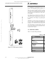
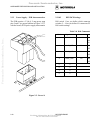
EVB Connector, Switch, and Jumper Header Location Diagram..................................... 2-2
Power Supply Connector (P7)......................................................................................... 2-18
Expansion Connector P6 Pin Assignments ..................................................................... 2-20
Expansion Connector P7 Pin Assignments ..................................................................... 2-21
EVB Block Diagram ......................................................................................................... 3-2
EVB Memory Map............................................................................................................ 3-6
© MOTOROLA Inc., 19
For More Information On This Product,
Go to: www.freescale.com
MPC505EVB/D
Freescale Semiconductor, Inc.
Freescale Semiconductor, Inc...
CONT
CHAPTER
GEN
Motorola reserves the right to make changes without further notice to any products
herein to 1
improve reliability, function, or design. Motorola does not assume any liability arising out of the
1.1 INTRODUCTION......................................
application or use of any product or circuit described herein; neither
does it convey any license
1.2
FEATURES................................................
under its patent rights nor the rights of others. Motorola products are not designed, intended, or
1.3implant
GENERAL
authorized for use as components in systems intended for surgical
into theDESCRIPTION
body, or other ......................
....................................
application in which the failure of the Motorola product could 1.4
create SPECIFICATIONS
a situation where personal
1.5 EQUIPMENT
REQUIRED........................
injury or death may occur. Should Buyer purchase or use Motorola
products for
any such
unintended or unauthorized application, Buyer shall indemnify and hold Motorola and its
officers, employees, subsidiaries, affiliates, and distributors harmless
against all
costs,
CHAPTER
2 claims,
HARDWARE
PRE
damages, and expenses, and reasonable attorney fees arising out of, directly or indirectly, any
claim of personal injury or death associated with such unintended
unauthorized use, even if
2.1 orINTRODUCTION......................................
such claim alleges that Motorola was negligent regarding the design
manufacture of
the part.
2.2 orHARDWARE
PREPARATION
................
2.2.1 Crystal Clock Select Header (J1) ......
Motorola and the Motorola logo are registered trademarks of Motorola
2.2.2Inc. Clock Source Select Header (J2).......
2.2.3 Keep Alive Power 2 Select Header (J
Motorola Inc. is an Equal Opportunity/Affirmative Action Employer.
2.2.4 Keep Alive Power 2 Select Header (J
2.2.5 Burst Memory Select Header (J5) .....
PowerPC is a trademark of International Business Machines Corporation.
2.2.6 System Clock Selection Headers (J6
2.2.7 EVB LED Descriptions .....................
2.2.8 Optional Memory Configuration.......
2.2.9 EVB Reset Switches..........................
2.2.10 EVB DIP Switches ............................
2.2.10.1 Chip Select Dip Switch (DS1)..
2.3.10.2 Reset Data Dip Switches (DS2
2.2.10.3 DTE/DCE Settings ...................
2.3 INSTALLATION INSTRUCTIONS.........
2.3.1 Host Computer – EVB Interconnecti
2.3.2 Background Mode Connector (P5)....
2.3.3 Power Supply – EVB Interconnectio
2.3.4 RS-232C – EVB Interconnection ......
2.3.5 EVB Expansion Connectors..............
2.3.6 Logic Analyzer Connectors...............
2.3.7 SCSI...................................................
MPC505EVB/D
For More Information On This Product,
Go to: www.freescale.com
Freescale Semiconductor, Inc.
GENERAL INFORMATION
TAB
Freescale Semiconductor, Inc...
1.3 GENERAL DESCRIPTION
1-1. EVB Specifications ....................................
1-2. External
Equipment
Requirements
............
The EVB is a low-cost tool for evaluating and debugging MPC505
MCU-based
systems.
The
MPC505 MCU device is an advanced single-chip MCU with2-1.
on-chip
memory
andTypes.................................
peripheral
Jumper
Header
functions. For more information refer to the PowerPC MPC5052-2.
RISCMPFB
Microcontroller
Technical
Jumper Header
Descriptions...........
Summary (MPC505TS/D).
2-3. MF and RFD Bits Required to Set Clock S
2-4.
System Clock
Source Configuration..........
The EVB includes a monitor/debugging program (MPCbug) that
demonstrates
the capabilities
of
2-5.
Optional
Memory
Configuration................
the MPC505. You can debug user code under control of the MPCbug monitor program, assemble
2-6. it to
Chip
Select Dip Switch (DS1) ...................
it (as either a Motorola S-record, COFF, or ELF file) and download
RAM.
2-7. Data Bus Reset Configuration Word..........
The Motorola S-record format lets you encode programs or data
in aCommunication
printable format
for Switch Setting
2-8.filesDS6
Type
transportation between computer systems. The transportation process can therefore be monitored
2-9. SCSI Port Parts List....................................
and the S-records easily edited. Refer to Appendix A for additional S-record information.
4-1. SCSI Connector (not populated) ................
Connector
The EVB has one host computer port (P4), two RS-232C 4-2.
serial RS-232C
ports (P2I/O
and
P3) and P2
a Pin Assignmen
4-3. (DB-25
RS-232Cconnector)
I/O Connector
P3 Pin Assignmen
background debug mode port (P5). The host computer port
is for
downloading S-records and communicating with the EVB 4-4.
via a Host
host Computer
computer.Connector
You canP4 Pin Assignm
configure P4 as DTE or DCE. P4 is fixed at 19200 baud. P2 and
(DB-9Mode
connectors)
on the
4-5. P3Debug
Connector
P5 Pin Assignmen
EVB are RS-232C I/O ports. These two I/O ports let you evaluate
MPC505
control
of
RS-232
4-6. P6 Expansion Connector Pin Assignments
communication. These ports can be configured as either data computer equipment (DCE) or data
4-7. Input Power Connector P7 Pin Assignmen
terminal equipment (DTE) protocol via a set of switches. (An example of DCE is a modem and
4-8. at P8
Connector Pin Assignments
DTE a computer terminal). These serial ports are available to you
all Expansion
times; the development
4-9. baud
Logic
Analyzer
system monitor, MPCbug, does not require these ports. Supported
rates
for P2 Connector
and P3 arePOD1 Pin Assi
4-10.
Logic MCU
Analyzer
Connector POD2 Pin Assi
1200 to 19200. P5 (10-pin berg) lets you communicate with the
MPC505
in background
4-11. Logic Analyzer Connector POD3 Pin Assi
debug mode.
4-12. Logic Analyzer Connector POD4 Pin Assi
The EVB requires a user-supplied +5 Vdc power supply. The power
voltage isConnector
converted POD5 Pin Assi
4-13. supply
Logic Analyzer
to +3.3 Vdc by the EVB on-board voltage converter. +3.3 Vdc is the voltage required by the
4-14. Logic Analyzer Connector POD6 Pin Assi
MPC505 MCU.
4-15. Logic Analyzer Connector POD7 Pin Assi
The EVB comes with a 4 MHz crystal and a socket for a crystal oscillator. The EVB is factory
configured to use the 4 MHz crystal as the input. You can increase the clock frequency up to 33
MHz (refer to paragraph 2.2.8).
All MPC505 MCU signals are available, unbuffered, on the expansion connectors and logic
analyzer connectors. The logic analyzer connectors let you monitor MPC505 MCU activity
during the development stage.
There are four flash memory devices (U24, U25, U27, and U28) on the EVB that provide 512
kilobytes of program storage memory. These devices are organized as long-word (32 bits wide).
You may program on-board flash memory using the MPCbug commands to download the
program via the debug port and run the programming algorithm. Flash memory may be upgraded
1-2
MPC505EVB/D MPC505EVBUM/D
For More Information On This Product,
Go to: www.freescale.com
Freescale Semiconductor, Inc.
CONTENTS
CHAP
GENERAL IN
1.1 INTRODUCTION
Freescale Semiconductor, Inc...
This manual provides general information, hard
support information for the MPC505EVB Evalu
PowerPC MPC505 RISC Microcontrollers.
1.2 FEATURES
EVB features include:
vi
•
MPC505 MCU running at 4-33 MHz
•
512 kilobytes of flash memory (may b
•
128 kilobytes of synchronous static R
•
Serial port with 25-pin RS-232 conne
•
MC68681 DUART providing two ser
•
MC68HC711 MCU for the backgroun
•
SCSI-2 port (optional)
•
Expansion connectors for the MPC50
•
20-pin logic analyzer connectors for t
•
5-volt-to-3.3-volt converter for the M
•
Reset data configuration switches
•
Crystal or crystal oscillator operation
MPC505EVBUM/D
MPC505EVB/D *PRELIMINARY
For More Information On This Product,
Go to: www.freescale.com
Freescale Semiconductor, Inc.
HARDWARE PREPARATION AND INSTALLATION
to 2 megabytes by replacing the devices at lo
devices. The flash memory devices require +5 vo
There are a total of eight 52-pin PLCC sockets
U31, and U32) for synchronous static RAM (SSR
and lower words and organized for long-word (3
to as BANKx.
Freescale Semiconductor, Inc...
The SSRAM factory default for the EVB is 128
These devices have 9 nanosecond access times an
be expanded to 256 kilobytes by replacing the
devices.
Alternately, you may increase the amount of on
U30, U31, and U32 with additional SSRAM dev
megabytes. (For information on increasing on-bo
The EVB includes an optional SCSI-2 port con
not provided, and the user may add them if the S
are provided in Chapter 2.
1.4 SPECIFICATIONS
Table 1-1 lists the EVB specifications.
Table 1-1. EVB
Characteristics
MCU
I/O ports:
I/O devices
Host computer
RSRS-
Temperature:
Operating
Storage
+25
0 to
0 to
Relative
humidity
Figure 2-1. EVB Connector, Switch, and Jumper Header Location
Diagram
2-2
MP
MP
0 to
Power requirements
+5 V
Dimensions:
9.17
MPC505EVBUM/D
MPC505EVBUM/D
For More Information On This Product,
Go to: www.freescale.com
Freescale Semiconductor, Inc.
GENERAL INFORMATION
1.5 EQUIPMENT REQUIRED
CHAP
Table 1-2 lists the external equipment requirements for EVB operation.
HARDWARE PREPARATI
Table 1-2. External Equipment Requirements
External Equipment
+5 Vdc power supply
Freescale Semiconductor, Inc...
SUN host computer
2.1 INTRODUCTION
This chapter provides unpacking instructions, ha
for the EVB. Chapter 6 is a description of the EV
RS-232C cable assembly
2.2 HARDWARE PREPARATION
This paragraph describes the preparation of EV
ensure that the EVB components are properly co
shipped with factory-installed jumpers. Figure 2header locations. The EVB consists of:
1-4
•
Dip switch DS1 lets you disconnect th
the target board.
•
Dip switches DS2 through DS5 define
•
Dip switch DS6 sets P2 ,P3 ,P4 and fo
•
Jumper headers J1 through J7 are for
2-2 and paragraphs 2.2.1 through 2.2.
•
Connector P1 is a SCSI interface conn
•
Connectors P2 and P3 let you conne
purposes.
•
Connector P4 is the serial port for
computer. You must supply your own
•
Connector P5 is the debug mode port
debug mode.
•
Expansion connectors P6 and P8 let
board.
•
Connector P7 is the EVB +5 Vdc pow
•
POD1 through POD7 are 20-pin lo
MPC505 MCU signals.
•
Switch SW1 lets you reset the MPC50
•
Switch SW2 lets you reset the EVB.
MPC505EVBUM/D
MPC505EVBUM/D
For More Information On This Product,
Go to: www.freescale.com
Freescale Semiconductor, Inc.
HARDWARE PREPARATION AND INSTALLATION
2.2.2
Clock Source Select Header (J2)
Freescale Semiconductor, Inc...
Table 2-1. Jump
Use jumper header J2 to select either a crystal or clock oscillator as the MCU clock source. The
drawing below shows the factory configuration: bus wire soldered
on Header
pins 2 and 3. This
Jumper
configuration selects the crystal clock source; crystal in socket at locatedType
Y1. When youSymbol
want to
use the clock oscillator as the EVB clock, move the bus wire on J2 from pins 2 and 3 to pins 1
two-pin with solder
and 2 and remove the bus wire on J1 (see paragraph 2.2.1). This disconnects
the MCU XTAL pin Two-pin plate
strap
designated as
from the crystal clock circuit at location Y1 and selects the crystal oscillator (U7) as the MCU soldered betw
clock source. The frequency of the crystal clock circuit is 4 MHz. The frequency of the crystal create a short.
oscillator circuit can be as fast as 40 MHz.
2.2.3
2
Two-pin jumpe
header numbe
between the tw
two-pin with jumper
Two-pin jumpe
jumper header
three-pin
Three-pin jump
header numbe
between two o
three-pin with jumper
Three-pin jump
the jumper hea
configuration,
Bus Wire
J2
3
two-pin
1
Keep Alive Power 2 Select Header (J3)
Jumper header J3 provides power to the MCU-internal RAM module via the MCU VKAPWR2
pin. You may use either the on-board +3.3 Vdc (jumper on J3 pins 1 and 2) or connect an
Table 2-2. MPFB Jump
external +3.3 Vdc power supply to J3 pins 2 and 3. An external +3.3 Vdc power supply on J3
pins 2 and 3 will maintain MCU-internal RAM data after EVB power
is turned OFF. To attach
Jumper
an external power supply to VKAPWR2: remove the jumper on J3 pins
1 and 2, and
connect the
Header
Type
power supply ground to J3 pin 3 and +3.3 Vdc to pin 2.
21
J1
Crystal clock
sourcr select
header
(XTAL)
J2
Bus wire between pins 1
clock source as the MCU
321
Clock
oscillator
source select
header
(EXTAL)
CAUTION
J3
Bus wire between pins 1
source as the MCU EXT
between pins 1 and 2 on
Bus wire soldered betwe
on-board 4 MHz crystal
321
Applying power to the EVB with J4 removed and no external
Keep alive
power supply attached to J4 will damage the power
MPC505
MCU.
2 select
Always keep a jumper or an external +3.3 Vdc power
supply on J4
header
pins 1 and 2. If using an external power supply, apply VKAPWR1
before powering up the EVB.
2-6
Bus wire soldered betwe
on-board 4 MHz crystal
Jumper installed on pins
active as long as power
VKAPWR2 pin of the MC
+3.3 Vdc external powe
internal RAM after EVB
MPC505EVBUM/D
MPC505EVBUM/D
For More Information On This Product,
Go to: www.freescale.com
Freescale Semiconductor, Inc.
HARDWARE PREPARATION AND INSTALLATION
2.2.1(continued)
Crystal Clock Select Header (J1)
Table 2-2. MPFB Jumper Header Descriptions
Jumper
Header
Type
J4
321
Freescale Semiconductor, Inc...
Keep alive
power 1 select
header
J5
J6,
System clock
selection
header
J7
System clock
selection
header
Jumper header J1 connects the crystal clock to t
shows the factory configuration: bus wir
the
crystal clock
source; crystal in socket
Jumper installed on pins 1 and 2 (factoryselects
default);
MCU-internal
oscillator,
oscillator
as
the
EVB
clock,
time base, and decrementer operates as long as power is applied to theremove the bus wire
and
1 and 2 (see paragraph 2.2.2). T
EVB (+3.3 Vdc present on the VKAPWR2
pin3ofto
thepins
MCU).
crystal clock circuit at location Y1 and selects the
+3.3 Vdc external power supply attached to jumper header J4 pins 2 and 3;
The frequency
of the operates
crystal clock circuit is 4 MH
maintains MCU-internal oscillator, time base,
and decrementer
can be as fast as 40 MHz.
after EVB power is turned OFF.
Description
below
Unused
3
2
1
Jumper installed on pins 1 and 2 (factory default); jumper headers J6 and
J7 select the MCU clock mode. The state of this signal during reset selects
the source of the system clock.
3
2
1
Jumper installed on pins 1 and 2 (factory default); jumper headers J6 and
J7 select the MCU clock mode.
J1
2
1
The EVB comes with a 4 MHz crystal and a soc
configured to use the 4 MHz crystal as the input.
MHz by setting the MF bits (bits 9-12) and RF
0x8007_FC50 (shown in Table 2-3).
Table 2-3. MF and RFD Bits
CLKO
RFD [0:3]
2-4
MF=
X000
(X4)
MF=
X001
(X5)
MF=
X010
(X6)
MF
X0
(X
0 = 0000
16
20
24
2
1 = 0001
8
10
12
1
2 = 0010
4
5
6
7
3 = 0011
2
2.5
32
3.
4 = 0100
1
1.25
1.5
1.7
5 = 0101
.5
.625
.75
.87
6 = 0110
.25
.313
.375
.43
7 = 0111
.125
.156
.188
.21
MPC505EVBUM/D
MPC505EVBUM/D
For More Information On This Product,
Go to: www.freescale.com
Freescale Semiconductor, Inc.
HARDWARE PREPARATION AND INSTALLATION
2.2.4
2.2.9
EVB Reset Switches
Freescale Semiconductor, Inc...
There are two reset switches on the EVB:
•
Switch SW1 lets you reset the MPC505 MCU
•
Switch SW2 lets you reset the EVB.
Keep Alive Power 2 Select Header (J4)
Jumper header J3 provides power to the MCU
modules via the MCU VKAPWR1 pin. You may
pins 1 and 2) or connect an external +3.3 Vdc po
Vdc power supply on J4 pins 2 and 3 will mainta
turned OFF. To attach an external power supply
and 2, and connect the power supply ground to J4
2.2.10 EVB DIP Switches
There are six DIP switches on the EVB (DS1 – DS6):
•
DS1 – Attaches the MCU chip selects to the EVB on-board memory and peripheral
devices. You may disable on-board chip selects and connect them via the expansion
connectors (P6 and P8) to external memory or peripheral devices.
•
DS2, DS3, DS4, DS5 – Data Bus Reset Configuration Word
•
DS6 – On the EVB are 3 RS232 ports (P2, P3, & P4) and one background debug
mode connector (P5). Each of the RS-232 ports can be either DTE or DCE port
(defined by DS6 switches 2, 3 and 4). While the host computer may be connected to
CAUT
the RS-232 port or the debug mode connector (DS6 switch 1).
Applying power to the EVB wi
power supply attached to J4 w
Always keep a jumper or an exter
pins 1 and 2. If using an external
before powering up the EVB.
2.2.5
Burst Memory Select Header (J5)
Unused.
2-10
MPC505EVBUM/D
MPC505EVBUM/D
For More Information On This Product,
Go to: www.freescale.com
Freescale Semiconductor, Inc.
HARDWARE PREPARATION AND INSTALLATION
2.2.6
System Clock Selection Headers (J6 and J7)
2.2.7
EVB LED Descriptions
Jumper headers J6 and J7 let you define the system clock source.
There are
Thethree
factory
LEDsconfiguration
on the EVB. Their function
(shown below) is for normal operation; a fabricated jumper on J6 and J7 pins 1 and 2. Refer to
• LD1 – 3.3 Vdc power: ON = 3.3 Vdc
Table 2-4 for configuring the system clock source.
• LD2 – Debug Mode: ON = MPC505
Freescale Semiconductor, Inc...
• LD3 – +5 Vdc power: ON = power is
Table 2-4. System Clock Source Configuration
MODCLK (J6)
Jumper Settings
VDDSYN (J7)
Jumper Settings
System Phase-LockLoop Options
1 and 2 (default)
1 and 2 (default)
2 and 3
1 and 2
1:1 Mode
1 and 2
2 and 3
SPLL Bypass Mode
2 and 3
2 and 3
Normal Operation
2.2.8
Optional Memory Configuration
There are eight 52-pin PLCC sockets on the EV
U32) for synchronous static RAM (SSRAM) d
lower
Special
Testwords
Mode and organized for long-word (32 bit
BANKx. Table 2-5 shows on-board, memory con
J6
Table 2-5. Optional M
3
Bank
Upper Word
Lower
BANK1
U29
U1
BANK2
U30
U2
1 BANK3
U31
U2
BANK4
U32
U2
2
Fabricated Jumpers
J7 The SSRAM factory default for the EVB is 128
(U19 and U29). You may increase the amou
3
increasing
the memory in sockets U19 and U29
populating U20, U21, U22, U30, U31, and U32
The2EVB can have up to 1 megabyte of on-board
1
2-8
MPC505EVBUM/D
MPC505EVBUM/D
For More Information On This Product,
Go to: www.freescale.com
Freescale Semiconductor, Inc.
HARDWARE PREPARATION AND INSTALLATION
Table 2-7. Data Bus Reset Configuration Word
2.2.10.1
(continued)
Chip Select Dip Switch (DS1)
Data
Bus
Bit
Configuration
Function
Effected
24
LEN
Freescale Semiconductor, Inc...
25
26
PRUMODE
ADDR[12:15]
Effect of
Mode Select = 1
During Reset
L-bus Memory modules
are enabled.
No effect
ADDR[12:15]
PB[4:7]
Reserved
28
Reserved
29
Reserved
31
2-14
disabled and emulated
externally.
Forces accesses to Ports
A, B, I, J, K, and L to go
external.
27
30
Effect of MCU uses several
EVB chip selects on-b
The MPC505
Mode
Select
=
0
Default
peripheral devices). You can redefine these ch
During Reset
Mode
expansion connectors. To avoid conflicts betwe
chip select
the appropriate
L-busappropriate
Memory modules
are by setting
1
Test Slave Mode Enable Test Slave Mode
Disabled
Test Transparent Mode Test Transparent Mode
Enable
Disabled
Table 2-6. Chip Sele
0
Pin
Chip Select
1
CSBOOT
2
FOE
3
CS1
4
CS2
5
CS3
Test Slave Mode Enabled
6
CS4
Test Transparent
Mode
7
Enabled
8
CS5
—
D
1
0
0
0
1
Flash chip select (U
Flash output enable
Burst RAM Bank1 (
Burst RAM Bank2 (
Burst RAM Bank3 (
Burst RAM Bank4 (
1 SCSI DUART (U4)
UNUSED
MPC505EVBUM/D
MPC505EVBUM/D
For More Information On This Product,
Go to: www.freescale.com
Freescale Semiconductor, Inc.
HARDWARE PREPARATION AND INSTALLATION
2.3.10.2
Reset Data Dip Switches (DS2 – DS5)
Table 2-7. Data Bus Reset Co
Data
Configuration
Dip switches DS2 – DS5 are connected through 4 buffers on the MPC505
MCU
data bus (D31 –
Bus
Function to these
D0). At RESET the MCU reads the data bus and changes its configuration according
Bit
Effected
switches ("ON" = 0 LOGIC).
Freescale Semiconductor, Inc...
[9:10]
IMEMBASE[0:1]
Effect o
Mode Selec
During Re
IMEMBASE
There are two reset configuration modes: data bus configuration mode (pertinent to the EVB) or00
internal default mode. In either mode the configuration is set by the MCU driving a configuration01
word onto the internal data bus. Table 2-7 describes the configuration options. The EVB Default10
11
Mode column shows the default reset configuration word. The default reset data bus
configuration word is X9E5EF4A3. For information on the internal
configuration modeLMEMBASE
[11:12] reset LMEMBASE[0:1]
00
refer to the PowerPC MPC505 RISC Microcontroller Technical Summary, MPC505TS/D.
Table 2-7. Data Bus Reset Configuration Word
Data
Bus
Bit
Configuration
Function
Effected
0
Address Bus
1
Vector Table Location
(IP Bit)
Vector Table
0xFFF0 0000
2
Burst Type/Indication
Type 2/LAST
3
Interface Type for
CSBOOT
4
CSBOOT Port Size
5
Reset Configuration
Source For DATA[6:13]
Latch Configuration from
external pins.
[6:8]
TA Delay For CSBOOT
TA Delay Encoding
000
001
010
011
100
101
110
111
13
Reset configuration
Latch configuratio
Effect
of for DATA[14:21]
EVB external pins
source
Mode Select = 0
Default
During
Reset
14
CT[0:3], AT[0:1],Mode
TS
CT[0:3], AT[0:1],
Effect of
Mode Select = 1
During Reset
Minimum Bus Mode
ADDR[0:11] = CS[0:11]
01
10
11
Maximum15Bus Mode WR, BDIP
1
ADDR[0:11] = Address Pins
16
PLLL/DSDO, VF[0:2],
Vector Table
VFLS[0:1], WP[1:5]0
0x0000 0000
17
BURST, TEA, AACK,
Type 1/BDIP
TA, BE[0:3] 0
WR, BDIP
ITYPE = 001
Asynchronous (Time to
Hi-Z = 2Clk)
ITYPE = 18
1000 CR, BI, BR, BB, BG,
1
Synchronous Burst
ARETRY
Bus Arbitration P
32-Bit
16-Bit
DSDO, Pipe Trac
Watchpoints
Handshake Pins
19
2-12
Release reset when PLL Release reset wh
1
locked
locked and after 1
(when not in PLL
Latch Configuration from
1
mode)
internal defaults.
20
Reserved
# of Wait States
100
0
21
Reset Configuration
Latch Configurati
1
Source For DATA[22:31] external pins.
2
22
Reserved
3
4
23
IEN
I-bus Memory mo
5
are enabled.
6
7
MPC505EVBUM/D
MPC505EVBUM/D
For More Information On This Product,
Go to: www.freescale.com
Freescale Semiconductor, Inc.
HARDWARE PREPARATION AND INSTALLATION
2.3.3
Power Supply – EVB Interconnection
2.2.10.3
DTE/DCE Settings
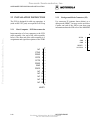
The EVB requires +5 Vdc @ 2 amp power supply for operation.
DS6
Connector
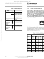
switch 1P7lets
pinyou
1 is define
+5 Vdc;
which connector
pins 2 and 3 are ground (shown in Figure 2-2). Use 16-22 AWG
switches
wire in2the
- 4connector
lets you define
(supplied
I/O connectors P2
with the board). EVB power supply interconnection for connector
DS6
P7switch
is shown
settings.
below.
Freescale Semiconductor, Inc...
Table 2-8. DS6 Communic
Pin #
Signal Name
Connector
1
OEDSDIDSCK
P4/P5
Swi
Swi
I/O
2
ADCE_DTE~
P2
ON
OFF
3
BDCE_DTE~
P3
ON
OFF
4
CDCE_DTE~
P4
ON
OFF
5
—
6
—
7
—
8
—
Figure 2-2. Power Supply Connector (P7)
2-18
MPC505EVBUM/D
MPC505EVBUM/D
For More Information On This Product,
Go to: www.freescale.com
Freescale Semiconductor, Inc.
HARDWARE PREPARATION AND INSTALLATION
2.3 INSTALLATION INSTRUCTIONS
2.3.2
Background Mode Connector (P5)
Freescale Semiconductor, Inc...
connector
P5 host
(pinouts
shown below) to co
The EVB is designed for table top operation. A user supplied Use
power
supply and
computer
debug
mode
(BDM).
You
may
use the serial deve
(with an RS-232C port) are required for EVB operation.
Connect one end of the SDI to your host comp
information about the SDI refer to the M68SDIU
2.3.1 Host Computer – EVB Interconnection
Interconnection of a host computer to the EVB is accomplished via a user supplied 25-pin flat
cable assembly. One end of the cable assembly is connected to the EVB connector P4 (shown
below). The other end of the cable assembly is connected to the host computer. For connector pinVFLS0
assignments and signal descriptions of the EVB I/O port connector P4, refer to Appendix B.
GND
P4
NC
CTXD
CRXD
CRTS
CCTS
CDSR
GND
CDCD
NC
NC
NC
NC
NC
1
2
3
4
5
6
7
8
9
10
11
12
13
14
15
16
17
18
19
20
21
22
23
24
25
1
•
3
•
GND
5
•
RESET~
7
•
VCC/V3.3
9
•
NC
NC
NC
NC
NC
NC
CDTR
NC
NC
NC
NC
NC
HOST COMPUTER
2-16
P
MPC505EVBUM/D
MPC505EVBUM/D
For More Information On This Product,
Go to: www.freescale.com
Freescale Semiconductor, Inc.
HARDWARE PREPARATION AND INSTALLATION
2.3.6
Logic Analyzer Connectors
2.3.4
RS-232C – EVB Interconnection
Freescale Semiconductor, Inc...
Use connectors POD1 through POD7 to connect a logic analyzer
Interconnection
to the circuit of
being
an evaluated.
RS-232C compatible de
Below are the pin assignments for the logic analyzer connectors.supplied 9-pin cable assembly. One end of the ca
or P3 (shown below). The other end of the cable
POD1
232CPOD2
compatible device. For connector pin assig
NC 1
•
• 2 NC
NC 232C
1 • ports
• P2
2 and
NCP3, refer to Appendix B.
TS~
3
•
•
4
FOE~
NC
3
•
•
4
A16
CS1~
5
•
•
6
CS2~
A17
5
•
•
6
A18
CS3~
7
•
•
8
CS4~
A19
7
•
•
8
A20
9
•
•
10 BSWE0~
A21
BSWE1~ 11
•
•
12 BSWE2~
A23 11
BSWE3~ 13
•
•
14 A10
A25 13
A11 15
•
•
16 A12
A27 15
A13 17
•
•
18 A14
A29 17
A15 19
•
•
20 GND
CS5~
9
(A31) GND 19
POD3
2-22
P2
• ADCD
• 10 1 A22
6
• ARXD
• 12 2 A24
7
• ATXD
• 14 3 A26
8
• ADTR
• 16 4 A28
• GND
• 18 5 GND (A30) 9
•
•
POD4
ADSR
ARTS
ACTS
NC
20 GND
RS-232 DEVICE
NC
1
•
•
2
NC
NC
1
•
•
2
NC
NC
3
•
•
4
D16
NC
3
•
•
4
D0
D17
5
•
•
6
D18
D1
5
•
•
6
D2
D19
7
•
•
8
D20
D3
7
•
•
8
D4
D21
9
•
•
10 D22
D5
9
•
•
10 D6
D23 11
•
•
12 D24
D7 11
•
•
12 D8
D25 13
•
•
14 D26
D9 13
•
•
14 D10
D27 15
•
•
16 D28
D11 15
•
•
16 D12
D29 17
•
•
18 D30
D13 17
•
•
18 D14
D31 19
•
•
20 GND
D15 19
•
•
20 GND
MPC505EVBUM/D
MPC505EVBUM/D
For More Information On This Product,
Go to: www.freescale.com
Freescale Semiconductor, Inc.
HARDWARE PREPARATION AND INSTALLATION
2.3.5
C
EVB Expansion Connectors
+3.3 Vdc
1
•
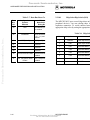
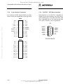
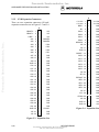
There are two expansion connectors (P6 and P8) on the EVB. The pin assignments for the
+3.3
expansion connectors are in Figures 2-3 and 2-4. Signal descriptions are in Appendix
B. Vdc 2 •
Freescale Semiconductor, Inc...
C
B
+3.3 Vdc
BDIP~
3
•
GND
A
BI~
4
•
GND
IRQ3~
5
•
GND
IRQ2~
6
•
GND
IRQ1~
7
•
GND
IRQ0~
8
•
GND
MODCLK
9
•
GND
NC 10
•
GND
NC 11
•
GND
GND 12
•
GND
BURST~ 13
•
GND
WP0~ 14
•
GND
WP1~ 15
•
GND
WP2~ 16
•
GND
WP3~ 17
•
GND
WP4~ 18
•
GND
WP5~ 19
•
GND
NC 20
•
GND
AT0 21
•
GND
ECROUT 22
•
GND
BE0~ 23
•
GND
BE1~ 24
•
GND
BE2~ 25
•
GND
BE3~ 26
•
GND
NC 27
•
GND
CR~ 28
•
GND
PDWU 29
•
GND
NC 30
•
VCC
GND 31
•
VCC
GND 32
•
VCC
BSWE3~
1
•
VCC
1
•
FOE~
1
•
BSWE1~
2
•
VCC
2
•
CS5~
2
•
CSBT~
3
•
VCC
3
•
A10
3
•
A21
4
•
BSWE2~
3
•
A11
4
•
A22
5
•
BSWE0~
4
•
A12
5
•
A23
6
•
CS4~
6
•
A13
6
•
A24
7
•
CS3~
7
•
A14
7
•
A25
8
•
CS2~
8
•
A15
8
•
A26
9
•
CS1~
9
•
A16
9
•
A27 10
•
GND 10
•
A17 10
•
A28 11
•
GND 11
•
A18 11
•
A29 12
•
GND 12
•
A19 12
•
GND 13
•
GND 13
•
A20 13
•
D16 14
•
GND 14
•
GND 14
•
D17 15
•
GND 15
•
D0 15
•
D18 16
•
GND 16
•
D1 16
•
D19 17
•
GND 17
•
D2 17
•
D20 18
•
GND 18
•
D3 18
•
D21 19
•
GND 19
•
D4 19
•
D22 20
•
GND 20
•
D5 20
•
D23 21
•
GND 21
•
D6 21
•
D24 22
•
GND 22
•
D7 22
•
D25 23
•
GND 23
•
D8 23
•
D26 24
•
GND 24
•
D9 24
•
D27 25
•
GND 25
•
D10 25
•
D28 26
•
GND 26
•
D11 26
•
D29 27
•
GND 27
•
D12 27
•
D30 28
•
GND 28
•
D13 28
•
D31 29
•
GND 29
•
D14 29
•
GND 30
•
CLKOUT 30
•
D15 30
•
NC 31
•
GND 31
•
GND 31
•
NC 32
•
GND 32
•
NC 32
•
Figure 2-4. Expansion Con
Figure 2-3. Expansion Connector P6 Pin Assignments
2-20
+3.3 Vdc
MPC505EVBUM/D
MPC505EVBUM/D
For More Information On This Product,
Go to: www.freescale.com
Freescale Semiconductor, Inc.
FUNCTIONAL DESCRIPTION
Freescale Semiconductor, Inc...
POD5
NC
1
•
•
2
NC
NC
3
•
•
4
DSCK
DSDI
5
•
•
6
DSDO
VF0
7
•
•
8
VF1
VF2
9
•
•
10 VFLS0
VFLS1 11
•
•
12 WP0~
WP1~ 13
•
•
14 WP2~
WP3~ 15
•
•
16 WP4~
WP5~ 17
•
•
18 NC
NC 19
•
•
20 GND
POD7
2.3.7
NC
1
•
•
2
NC
CLKOUT
3
•
•
4
BURST~
TEA~
5
•
•
6
AACK~
TA~
7
•
•
8
BE0~
BE1~
9
•
•
10 BE2~
BE3~ 11
•
•
12 BDIP~
R_W~ 13
•
•
14 TS~
AT0 15
•
•
16 AT1~
BI~ 17
•
•
18 ARETRY~
CSBT~ 19
•
•
20 GND
SCSI
The EVB printed circuit board includes an optio
port are user supplied. SCSI port parts list is prov
Table 2-9. SCSI
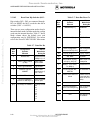
Figure 3-1. EVB Block Diagram
3-2
Reference Designation
P1
SCSI Conn
U1, U2
I.C., DS210
Semicondu
U3
I.C., 53C90
MPC505EVBUM/D
MPC505EVBUM/D
For More Information On This Product,
Go to: www.freescale.com
Freescale Semiconductor, Inc.
HARDWARE PREPARATION AND INSTALLATION
CHAP
FUNCTIONAL
3.1
INTRODUCTION
Freescale Semiconductor, Inc...
This chapter is a functional description of the EV
3.2
EVB DESCRIPTION
The EVB may be configured in either of two w
mounted on the target system. Figure 3-1 is the E
When the BCC is mounted on the PFB, you ma
code. To do this connect a terminal or host comp
debug monitor program. Logic analyzer connecti
the PFB.
Mount the BCC on the target system to verify h
target system, MC68332 MCU device emulat
connecting a PC to BCC connector P4 and run
connection may be made to connectors P1 and P2
2-24
MPC505EVBUM/D
MPC505EVBUM/D
For More Information On This Product,
Go to: www.freescale.com
Freescale Semiconductor, Inc.
FUNCTIONAL DESCRIPTION
XXX7FF
INTERNAL RAM
(2)
FFFFFF
MCU
INTERNAL
MODULES
FFF000
Freescale Semiconductor, Inc...
OPTIONAL RAM/EPROM
PFB: U2 & U4
CPU32BUG EPROM
BCC: U1 & U2
•
32-bit central processor unit (CPU32)
•
Time processor unit (TPU)
•
Queued serial module (QSM)
•
Random access memory (RAM)
7FF000
•
External bus interface
110000 /120000 (5)
•
Chip selects
•
System clock
•
Test module
FFE800
800000
ALTERNATE MCU
INTERNAL MODULES
LOCATION (4)
100000
0E0000
OPTIONAL RAM
PFB: U1 & U3
TARGET RAM
BCC: U3 & U4
SYSTEM RAM
BCC: U3 & U4
5.
The resident MC68332 Microcontroller Unit
designing, debugging, and evaluating MC68332
evaluation of prototype hardware/software produ
The MCU device is a 32-bit integrated micr
manipulation capabilities with powerful peripher
OPTIONAL FPCP (3)
PFB: U5
3.
4.
020000
010000
003000
CPU32BUG
3.3.1 INTERNAL
32-Bit Central
Processor Unit
STACK
CPU32BUG
The CPU32 is the central processor for the MC
INTERNAL
object code compatible with the MC68000 and
VARIABLES
unchanged. The CPU32 features are:
CPU32BUG VECTOR
• 32-Bit
internal data path and arithmet
TABLE
000000
Consult the MCU device user’s manual.
XXbase address is user programmable. Internal modules, such as
internal RAM, can be configured on power-up/reset by using the
initilization table (INITTBL) covered in Appendix C of the
M68MPCBUG Debug Monitor User’s Manual, M68MPCBUG /AD1.
Floating point coprocessor - MC68881/MC68882.
See Appendix C of the M68MPCBUG Debug Monitor User’s Manual,
M68MPCBUG /AD1.
Depends on the memory device type used.
Figure 3-2. EVB Memory Map
3-6
MCU SUMMARY
(1 )
XXX000
1.
2.
3.3
• 32-BitVECTOR
internal address bus - 24-bit ex
TARGET
TABLE
• Powerful instruction set
•
Eight 32-bit general purpose data regi
•
Seven 32-bit general purpose address
•
Separate user and supervisor stack po
•
Separate program and data address sp
•
Flexible addressing modes
•
Full interrupt processing
MPC505EVBUM/D
MPC505EVBUM/D
For More Information On This Product,
Go to: www.freescale.com
Freescale Semiconductor, Inc.
FUNCTIONAL DESCRIPTION
Freescale Semiconductor, Inc...
3.3.5
3.3.2
Time Processor Unit
3.3.3
Queued Serial Module
External Bus Interface
The external bus consists of 24 address lines and
sizing between
8- The
and TPU
16-bithas
data
The Time Processor Unit (TPU) optimizes performance of time-related
activities.
a accesses. A r
bus cycle
interruption.
External
dedicated execution unit, tri-level prioritized scheduler, data storage
RAM,
dual time bases,
and bus arbitration
interface.
microcode ROM which drastically reduces the need for CPU intervention. The TPU controls
sixteen independent, orthogonal channels; each channel has an associated I/O pin and can
perform any time function. Each channel also contains a dedicated
register,
for both match
3.3.6eventChip
Selects
and input capture functions.
Twelve independently programmable chip selec
Each channel can be synchronized to either of two 16-bit, free-running
counters
with
a pre-scaler.
peripheral
access.
Block
size is programmable f
One counter, based on the system clock, provides resolution ofcan
TPU
divided
by16-bit
4.
besystem
selectedclock
for either
8- or
transfers. A
The second counter, based on an external reference, also provides
resolution
of
TPU
system
insertion during the access. All bus interface sign
clock divided by 8. Channels may also be linked together,logic.
allowing the user to reference
operations on one channel to the occurrence of a specified action on another channel, providing
inter-task control.
3.3.7
System Clock
An on-chip phase locked loop circuit generates
16.78 MHz from a 32.768 kHz watch crystal. T
The QSM contains two serial ports. The queued serial peripheral
interfaceeither
(QSPI)
portperformance
provides
providing
high
or low pow
easy peripheral expansion or inter-processor communicationssystem
via a clock
full-duplex,
synchronous,
is a fully-static CMOS design, so it
three-line bus: data-in, data-out, and a serial clock. Four programmable
peripheral
select pins while still reta
via a low power stop instruction,
provide address-ability for as many as 16 peripheral devices. ARAM.
QSPI enhancement is an added
queue in a small RAM. This lets the QSPI handle as many as 16 serial transfers of 8- to 16-bits
each, or to transmit a stream of data as long as 256 bits without CPU intervention. A special
wrap-around mode lets the user continuously sample a serial peripheral,
automatically
3.3.8
Test
Module updating
the QSPI RAM for efficient interfacing to serial peripheral devices (such as analog-to-digital
The test module consolidates the microcontrol
converters).
production testing, user self-test, and system dia
The serial communications interface (SCI) port provides a standard
to zero checks
(NRZ) on internal log
providenon-return
signature analysis
mark/space format. Advanced error detection circuitry catches noise
glitches
to
1/16
of
a
bit
timeprovides a pass
pin to enter test mode. This test
in duration. Word length is software selectable between 8- or 9-bits,
and the SCI modulus-type,
vectors.
baud rate generator provides baud rates from 64 to 524k baud, based on a 16.77 MHz system
clock. The SCI features full- or half-duplex operation, with separate transmitter and receiver
3.4 andUSER
MEMORY
enable bits and double buffering of data. Optional parity generation
detection
provide either
even or odd parity check capability. Wake-up functions let the CPU run uninterrupted until either
On board the BCC is 32k x 16 bits of RAM an
a true idle line is detected or a new address byte is received.
debug monitor storage area and user accessib
Monitor is stored in the BCC EPROMs. For deb
3.3.4
Random Access Memory
Debug Monitor User’s Manual, M68MPCBUG /A
2k bytes of static RAM are contained within the MC68332 MCU
Thesockets
RAM for
is used
Thedevice.
PFB has
32k for
x 16 or 64k x 16
storage of variable and temporary data. RAM data size may beand/or
8-bitsEPROM,
(byte), 16-bits
(word),
supplied by theoruser, is user-acc
32-bits (longword). The RAM can be mapped to any 2k byte boundary in the address map.
3-4
MPC505EVBUM/D
MPC505EVBUM/D
For More Information On This Product,
Go to: www.freescale.com
Freescale Semiconductor, Inc.
SUPPORT INFORMATION
3.5
Pin
Freescale Semiconductor, Inc...
1
I/O CONNECTORS
Table 4-1. SCSI Connector (not populated)
There are two 64-pin expansion connectors on th
the BCC communicates with the PFB or target sy
Mnemonic
Signal
through P3 and serial communication through P4
GND
GROUND
interface connectors pin assignments.
2
SDB0
SCSI DATA BUS (bit 0) – Bit 0 of the SCSI bi-directional data bus lines.
3
GND
GROUND
4
SDB1
expansion
connectors
SCSI DATA BUS (bit 1) – Bit 1 of theThe
SCSI
bi-directional
data bus interconnect
lines.
5
GND
GROUND
6
SDB2
SCSI DATA BUS (bit 2) – Bit 2 of the SCSI bi-directional data bus lines.
7
GND
GROUND
8
SDB3
SCSI DATA BUS (bit 3) – Bit 3 of the SCSI bi-directional data bus lines.
9
GND
10
SDB4
A terminal or host computer with terminal emula
GROUND
be connected to the BCC or to the PFB. Termi
communication connectors, BCC P4 or to PFB P
SCSI DATA BUS (bit 4) – Bit 4 of the SCSI bi-directional data bus lines.
11
GND
GROUND
12
SDB5
SCSI DATA BUS (bit 5) – Bit 5 of the SCSI bi-directional data bus lines.
13
NC
14
SDB6
15
GND
16
SDB7
17
GND
GROUND
18
SDBP
SCSI DATA BUS PARITY – SCSI bi-directional
dataDESCRIPTION
parity line.
3.6 PFB
19 – 25
GND
GROUND
26
VCC
+5 VDC POWER – Input voltage (+5 memory.
Vdc @ 2.0I/O
A) used
by the EVB
connectors
are available
logic circuits.
3.5.1
64-Pin Expansion Connectors
the BCC
MC68332 MCU device, serial communication, a
the expansion connectors.
3.5.2
3.5.3
Serial Communication Connectors
Background Mode Interface Connect
The background debug mode is implemented in M
can be viewed or altered, memory can be read
SCSI DATA BUS (bit 6) – Bit 6 of theBackground
SCSI bi-directional
lines. by one of seve
modedata
is bus
initiated
internal peripherally generated breakpoints, so
GROUND
Instruction execution is suspended for the dur
SCSI DATA BUS (bit 7) – Bit 7 of the SCSI bi-directional data bus lines.
communications between the BCC and the devel
Not Connected
The PFB is the physical location for installing the
for commu
3.6.1
Floating-Point Coprocessor Socket (U
Socket U5 on the PFB accommodates an optiona
or an MC68882 coprocessor can be used in sock
part of the EVB, so must be provided by the
interface, see the application note MC68881 Fl
M68000 System, AN947.
4-2
MPC505EVBUM/D
MPC505EVBUM/D
For More Information On This Product,
Go to: www.freescale.com
Freescale Semiconductor, Inc.
FUNCTIONAL DESCRIPTION
The coprocessor interface is a transparent, logical extension of the MC68332 MCU device
registers and instructions. To the external environment the CPU and coprocessor execution
model appear to be on the same chip.
CHAP
Freescale Semiconductor, Inc...
SUPPORT INF
A coprocessor interface is an execution model based on sequential instruction execution by the
CPU and coprocessor. For optimum performance, the coprocessor interface lets floating point
instructions execute concurrently with CPU integer instructions. Concurrent instruction
4.1 INTRODUCTION
execution is further extended by the coprocessor, which executes
multiple floating-point
instructions simultaneously.
The tables in this chapter describe EVB connecto
3.6.2
Logic Analyzer Connectors
4.2 CONNECTOR SIGNAL DESCRIP
To debug hardware and software developed for the MC68331 MCU device, connect a logic
The following are all the connectors on the bo
analyzer to the desired pins of PFB connectors P1 - P6.
description.
Connector P7 connects external power to the EV
P4. POD1 through POD7 let you connect a logi
ports for evaluating RS-232C devices.
NO
The signal descriptions in the
reference only. For a complete
consult the appropriate MCU user
summary. For a complete descrip
the appropriate NCR 53C90B U
complete description of the P2,P
MOTOROLA M68681 User Man
Tables 4-1 through 4-19 list pin assignments for
3-8
Table 4-1
SCSI connector P1 (not populated)
Table 4-2
RS-232C I/O port P2
Table 4-3
RS-232C I/O port P3
Table 4-4
Host computer connector P4
Table 4-5
Debug mode connector P5
Table 4-6
Expansion connector P6
Table 4-7
Input power connector P7
Table 4-8
Expansion connector P8
MPC505EVBUM/D
MPC505EVBUM/D
For More Information On This Product,
Go to: www.freescale.com
Freescale Semiconductor, Inc.
SUPPORT INFORMATION
Freescale Semiconductor, Inc...
Table 4-4. Host Computer Connector P4 Pin Assignments
4-6
Signal
Table 4-1. SCSI Connector
Pin
Mnemonic
1
NC
2
CTXD
TRANSMIT – RS-232C serial output signal.32
3
CRXD
4
CRTS
RECEIVE DATA – RS-232C serial input signal.
33 – 35
GND
GROUND
REQUEST TO SEND – An input signal used to request permission to
36
BSY
BUSY – Active low I/
transfer data.
5
CCTS*
6
ADSR*
7
GND
8
CDCD*
9 - 19
NC
20
ADTR*
21 - 25
NC
Not Connected
Pin
Mnemonic
27 – 31
GND
GROUND
ATNI*
ATTENTION – Active
the MPC505 has a m
CLEAR TO SEND – An output signal that indicates
37
a ready-to-transfer
GND
GROUND
data status.
38
ACK
ACKNOWLEDGE – A
DATA SET READY – An output signal (held high) that indicates an on-target that the MPC5
line/in-service/active status.
39
GND
GROUND
GROUND
40
RST
RESET – Active-low
DATA CARRIER DETECT – An output signal used to indicate an
devices using the bu
acceptable received line (carrier) signal has been detected.
41
GND
GROUND
Not Connected
42
MSG
MESSAGE – ActiveDATA TERMINAL READY – An output line that indicates an on-line/insending a message.
service/active status.
43
GND
GROUND
Not Connected
44
SEL
SELECT – Active-low
target.
45
GND
GROUND
46
C/D
CONTROL/DATA – A
control of data is on t
47
GND
GROUND
48
REQ
REQUEST – Active-l
that the target has tra
49
GND
GROUND
50
I/O
INPUT/OUTPUT – A
controls data directio
MPC505EVBUM/D
MPC505EVBUM/D
For More Information On This Product,
Go to: www.freescale.com
Freescale Semiconductor, Inc.
SUPPORT INFORMATION
Table 4-2. RS-232C I/O Connector P2 Pin Assignments
Freescale Semiconductor, Inc...
Pin
Mnemonic
Signal
Pin
Table 4-3. RS-232C I/O Con
Mnemonic
1
ADCD*
DATA CARRIER DETECT – An output signal
1 used to indicate
BDCD*
an
acceptable received line (carrier) signal has been detected.
DATA CARRIER DE
acceptable received
2
ARXD
RECEIVE DATA – RS-232C serial input signal.
2
BRXD
RECEIVE DATA – R
3
ATXD
TRANSMIT – RS-232C serial output signal.3
BTXD
TRANSMIT – RS-23
4
ADTR*
DATA TERMINAL READY – An output line 4that indicatesBDTR*
an on-line/inDATA TERMINAL RE
service/active status.
service/active status.
5
GND
GROUND
6
ADSR*
DATA SET READY – An output signal (held6high) that indicates
BDSR*an on-DATA SET READY –
line/in-service/active status.
line/in-service/active
7
ARTS
REQUEST TO SEND – An input signal used7 to request permission
BRTS
toREQUEST TO SEND
transfer data.
transfer data.
8
ACTS*
CLEAR TO SEND – An output signal that indicates
8
a ready-to-transfer
BCTS*
CLEAR TO SEND –
data status.
data status.
9
NC
Not Connected
4-4
5
9
GND
NC
GROUND
Not Connected
MPC505EVBUM/D
MPC505EVBUM/D
For More Information On This Product,
Go to: www.freescale.com
Freescale Semiconductor, Inc.
SUPPORT INFORMATION
Freescale Semiconductor, Inc...
Table 4-8. P8 Expansion Connector Pin Assignments (continued)Table 4-5. Debug Mode Co
Pin
Mnemonic
A-21
NC
A-22
ARETRY*
A-23
BG*
A-24
BR*
BUS REQUEST – Active-low input signal that
an externalDEVELOPMENT SE
4 indicates that
DSCK
device requests bus mastership.
debug mode.
A-25
BB*
A-26
RESET*
BUS BUSY – Active-low, bi-directional signal5asserted by the
current GROUND
GND
master that indicates that the bus is in use.
6
VFLS1
VISIBILITY FLUSH
RESET – Active-low, input signal that resets the MPC505 MCU.
background debug m
A-27
SRESET*
A-28, A-29
VFLS1,
VFLS0
A-30
DSDI
A-31
DSCK
A-32
DSDO
B-1, B-2
V3.3
+3.3 VDC POWER – Voltage generated by the on-board voltage
converter for use by the MPC505 MCU logic circuits.
B-3 B-29
GND
GROUND
B-30 B-32
VCC
+5 VDC POWER – Input voltage (+5 Vdc @ 2.0 A) used by the EVB
logic circuits.
C-1, C-2
V3.3
+3.3 VDC POWER – Voltage generated by the on-board voltage
converter for use by the MPC505 MCU logic circuits.
C-3
BDIP*
4-10
Signal
Not Connected
Pin
Mnemonic
1
VFLS0
VISIBILITY FLUSH
background debug m
ADDRESS PHASE RETRY – An active-low input signal that indicates
the master needs to retry its address phase. 2
SRESET*
SYSTEM RESET –
asserted by the MC
BUS GRANT – Active-low input signal that indicates that an external
device has assumed control of the bus.
3
GND
GROUND
SYSTEM RESET – Active-low, MPC505 MCU
that resetsRESET – Active-low
7 output signal
RESET*
the EVB.
8
DSDI
DEVELOPMENT SE
VISIBILITY FLUSH – History buffer flush status bits that indicate how mode.
many instructions are flushed from the history buffer during the current
VCC
+5 VDC POWER –
clock cycle. Also indicates the freeze state. 9
logic circuits.
DEVELOPMENT SERIAL DATA IN – Serial data input signal for debug
10
DSDO
DEVELOPMENT SE
mode.
debug mode.
DEVELOPMENT SERIAL CLOCK – Serial input clock for background
debug mode.
DEVELOPMENT SERIAL DATA OUT – Serial data output signal for
debug mode.
BURST DATA IN PROGRESS – An active-low output signal that
indicates the data beat in front of the current one is needed by the
master.
MPC505EVBUM/D
MPC505EVBUM/D
For More Information On This Product,
Go to: www.freescale.com
Freescale Semiconductor, Inc.
SUPPORT INFORMATION
Freescale Semiconductor, Inc...
Table 4-6. P6 Expansion Connector Pin Assignments
Pin
Mnemonic
A-1
FOE*
FLASH OUTPUT ENABLE - Active low output
1 signal that VCC
lets you read
+5 VDC POWER – In
the EVB on-board flash memory.
logic circuits. The "VC
A-2
CS5*
A-3 A-13
A10 A20
CHIP SELECT 5 Output signal that selects2peripheral/memory
GND devices
GROUND The "GND
at programmed addresses.
3
GND
GROUND The "GND
ADDRESS BUS (bits 10 – 20) – 11-pins of the three-state output
address bus.
A-14
GND
A-15 A-30
D0 D15
A-31
GND
A-32
NC
B-1 B-3
VCC
B-4
BSWE2*
B-5
BSWE0*
B-6 B-9
CS4* CS1*
B-10 B-29
GND
B-30
CLKOUT
B-31, B-32
GND
C-1
BSWE3*
C-2
BSWE1*
C-3
CSBT*
C-4 C-12
A21 A29
C-13
GND
C-14 C-29
D16 D31
C-30
GND
C-31, C-32
NC
4-8
Signal Pin
Table 4-7. Input Power Con
Table 4-8. P8 Expansion C
GROUND
Pin
DATA BUS (bits 0 15) – Bi-directional data
pins.
GROUND
Not Connected
Mnemonic
Mnemonic
A-1, A-2
V3.3
+3.3 VDC POWER –
converter for use by
A-3
AACK*
ADDRESS ACKNOW
the slave has receive
+5 VDC POWER –Input voltage (+5 Vdc @ 2.0 A) used by the EVB
A-4
TS*
TRANSFER START
logic circuits.
start of a bus cycle.
Address signal A8 - one signal of the three-state output address bus.
A-5
VDDSYN
VDDSYN – Clock sy
Address signal A6 - one signal of the three-state output address bus.
INTERRUPT REQUE
A-6 A-8
IRQ6* –
CHIP SELECT (4 – 1) – Output signals that select peripheral/memory
IRQ4*
requests MCU synch
devices at programmed addresses.
A-9 A-12
CT0 CT3
CYCLE TYPE SIGNA
GROUND
the bus master is init
SYSTEM CLOCK OUT – Output signal that
is the MPC505
MCU
A-13
GND
internal system clock.
A-14 A-16
VF0 VF2
GROUND
GROUND
VISIBILITY FETCH –
fetched instruction or
instruction queue.
Address signal A9 - one signal of the three-state output address bus.
A-17
R_W*
READ/WRITE – Acti
Address signal A7 - one signal of the three-state output address bus.data transfer on the b
TA*peripheral
TRANSFER ACKNO
BOOT CHIP SELECT – Active-low outputA-18
signal that selects
indicates the slave h
or memory devices at programmed addresses.
data during a read cy
ADDRESS BUS (bits 21 29) – 9-pins of the three-state output address
A-19
TEA*
TRANSFER ERROR
bus.
indicates bus error co
GROUND
A-20
AT1
ADDRESS TYPES b
space as: user data,
DATA BUS (bits 16 31) – Bi-directional data pins.
instruction.
GROUND
Not Connected
MPC505EVBUM/D
MPC505EVBUM/D
For More Information On This Product,
Go to: www.freescale.com
Freescale Semiconductor, Inc.
SUPPORT INFORMATION
Freescale Semiconductor, Inc...
Table 4-14. Logic Analyzer Connector POD6 Pin Assignments
Table 4-8. P8 Expansion Connec
Pin
Mnemonic
1–3
NC
4
CLKOUT
5
RESET*
6
SRESET*
7 – 10
CT0 – CT3
11
CR*
12
BR*
13
14
15, 16
17
18
19
20
4-14
Signal
Not Connected
Pin
Mnemonic
C-4
BI*
SYSTEM CLOCK OUT – Output signal that is the MPC505 MCU
C-5, C-6
IRQ3* IRQ2*
internal system clock.
BURST INHIBIT – Ac
not support burst mo
INTERRUPT REQUE
requests MCU synch
RESET – Active-low, input signal that resets the MPC505 MCU.
C-7, C-8
IRQ1*, IRQ0* INTERRUPT REQUE
SYSTEM RESET – Active-low, MPC505 MCU output signal that resets
requests MCU synch
the EVB.
C-9
MODCK
CLOCK MODE SELE
CYCLE TYPE SIGNALS – Four bits that indicate what type of bus cycle
source of the interna
the bus master is initiating.
C-10, C-11
NC
Not Connected
CANCEL RESERVATION Active-low input that instructs the bus master
GND
GROUND
to clear the external device's reservation. C-12
BUS REQUEST – Active-low input signal C-13
that indicates that
BURST*
an external
BURST – Active low
device requests bus mastership.
C-14 C-17
WP0* – WP3* WATCHPOINT (0 - 3
BB*
BUS BUSY – Active-low, bi-directional signal asserted by the current watchpoint.
master that indicates that the bus is in use.
C-18, C-19
WP4*, WP5* WATCHPOINT (4, 5)
BG*
BUS GRANT – Active-low input signal that indicates that an external watchpoint.
device has assumed control of the bus.
C-20
NC
Not Connected
IRQ0*, IRQ1* INTERRUPT REQUEST (0, 1) – Prioritized active low input lines that
C-21has the highest
AT0priority. ADDRESS TYPES b
requests MCU synchronous interrupts. IRQ1*
space as: user data,
ECROUT
ENGINEERING CLOCK REFERENCE OUT Clock reference for
instruction.
peripheral chips.
C-22
ECROUT
ENGINEERING CLO
MODCLK
CLOCK MODE SELECT – Active-high input signal that selects the
peripheral chips.
source of the internal system clock.
C-23 C-26
BE0* BE3* BYTE ENABLE (03)
PDWU
POWER DOWN WAKEUP Output signal sends a power-down wakeup
controls one byte lan
to external power-on reset circuits.
C-27
NC
Not Connected
GND
GROUND
C-28
CR*
CANCEL RESERVA
to clear the external
C-29
PDWU
C-30
NC
C-31, C-32
GND
POWER DOWN WA
to external power-on
Not Connected
GROUND
MPC505EVBUM/D
MPC505EVBUM/D
For More Information On This Product,
Go to: www.freescale.com
Freescale Semiconductor, Inc.
SUPPORT INFORMATION
Freescale Semiconductor, Inc...
Table 4-9. Logic Analyzer Connector POD1 Pin Assignments
Table 4-12. Logic Analyzer Con
Pin
Mnemonic
Signal
Pin
Mnemonic
1, 2
NC
Not Connected
1–3
NC
3
TS*
4
FOE*
TRANSFER START – An active-low output
4 –signal
19 that indicates
D0 – D15the DATA BUS (bits 0 1
start of a bus cycle.
20
GND
GROUND
FLASH OUTPUT ENABLE - Active low output signal that lets you read
the EVB on-board flash memory.
5–9
CS1* – CS5*
10 – 13
BSWE0* –
BSWE3*
14 – 19
A10 – A15
20
GND
CHIP SELECT (1 – 5) – Output signals that select peripheral/memory
Table 4-13. Logic
devices at programmed addresses.
Mnemonic
1–3
NC
4 – 17
A16 – A29
18 – 20
GND
Analyzer Co
Address signal A6 - A9 - one signal of the three-state
output
address
Pin
Mnemonic
bus.
1–3
NC
Not Connected
ADDRESS BUS (bits 10 15) – 6-pins of the three-state output address
4
DSCK
DEVELOPMENT SE
bus.
debug mode.
GROUND
5
DSDI
DEVELOPMENT SE
mode.
Table 4-10. Logic Analyzer Connector POD2 Pin Assignments
6
DSDO
Pin
Not Connected
Signal
VISIBILITY FETCH –
fetched instruction or
instruction queue.
ADDRESS BUS (bits 16 29) – 14-pins of the three-state output address
bus.
10, 11
VFLS0,
VISIBILITY FLUSH –
VFLS1
many instructions are
GROUND
clock cycle. Also indi
Not Connected
7–9
DEVELOPMENT SE
debug mode.
12 – 15
VF0 – VF2
WP0* – WP3* WATCHPOINT (0 - 3
watchpoint.
Table 4-11. Logic Analyzer Connector POD3 Pin Assignments
Pin
Mnemonic
1–3
NC
4 – 19
D16 – D31
20
GND
4-12
Signal 16, 17
WP4*, WP5*
Not Connected
18, 19
DATA BUS (bits 16 31) – Bi-directional data pins.
20
GROUND
NC
GND
WATCHPOINT (4, 5)
watchpoint.
Not Connected
GROUND
MPC505EVBUM/D
MPC505EVBUM/D
For More Information On This Product,
Go to: www.freescale.com
Freescale Semiconductor, Inc.
SUPPORT INFORMATION
Freescale Semiconductor, Inc...
Table 4-15. Logic Analyzer Con
4-16
Pin
Mnemonic
1, 2
NC
3
CLKOUT
4
BURST
BURST – Active low
5
TEA*
TRANSFER ERROR
indicates bus error co
6
AACK*
ADDRESS ACKNOW
the slave has receive
7
TA*
TRANSFER ACKNO
indicates the slave h
data during a read cy
8 – 11
BE0* – BE3*
BYTE ENABLE (0 3
controls one byte lan
12
BDIP*
BURST DATA IN PR
indicates the data be
master.
13
R_W*
READ/WRITE – Acti
data transfer on the b
14
TS*
TRANSFER START
start of a bus cycle.
15, 16
AT0, AT1
ADDRESS TYPES (0
space as: user data,
instruction.
17
BI*
BURST INHIBIT – Ac
not support burst mo
18
ARETRY*
ADDRESS PHASE R
the master needs to
19
CSBT*
BOOT CHIP SELEC
or memory devices a
20
GND
Not Connected
SYSTEM CLOCK OU
internal system clock
GROUND
MPC505EVBUM/D
MPC505EVBUM/D
For More Information On This Product,
Go to: www.freescale.com