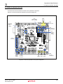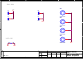
1
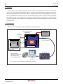
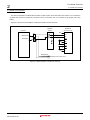
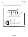
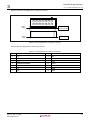
REJ10J0917-0100
PRELIMINARY
Notice This is not a final specification.
Some parametric limits are subject to change.
SH7149 CPU Board
M3A-HS49
32
User's Manual
Renesas 32-Bit RISC Microcomputers
SuperH RISC engine Family / SH7149 Group
TM
Rev. 1.0
Issued : Dec 15, 2006
Microsoft, MS-DOS, Windows and Windows.NET are registered trademarks of Microsoft Corporation of the U.S. in the U.S.
and other countries.
IBM and AT are registered trademarks of International Business Machines Corporation of the U.S.
Adobe and Acrobat are registered trademarks of Adobe Systems Incorporated.
All other brand names and product names are registered trademarks or trademarks of the respective proprietors.
Requests for Safety Design
• Renesas is constantly making efforts to improve the quality and reliability of its products. However, not
all semiconductor products are trouble-free, they may become faulty or operate erratically. To ensure
that no accidents such as injury or a fire or no social damage may arise from Renesas semiconductor
products should they become faulty or operate erratically, please pay careful attention to the safety
design of your system by, for example, considering redundancy design and incorporating measures to
check the spread of a fire and prevent device malfunction.
Precautions on Using This Manual
• This manual only provides reference information to help customers purchase the appropriate type of
Renesas Technology product that suits the intended purpose of use, and the technical information
contained herein does not implicitly or otherwise grant a license or rights to use the intellectual property or
other rights of Renesas Technology.
• Renesas Technology will not assume any responsibility for damage or losses or infringement on the third
parties’ rights arising from the use of product data, diagrams, tables, programs, algorithms or example
application circuits presented in this manual.
• The product data, diagrams, tables, programs, algorithms and all other information presented herein reflect
the latest that was available at the time this manual was issued, and Renesas Technology reserves the
right to change the products or specifications described herein without prior notice. When purchasing
Renesas Technology semiconductor products, please contact Renesas Technology or Renesas
Technology Sales or other distributors to obtain the latest information, and also keep abreast of the
information published at the Renesas Technology home page (http://www.renesas.com) or through other
media.
• The information contained herein was carefully prepared and is believed to be correct. However, Renesas
Technology will not assume responsibility for losses that the customers by any possibility may suffer
because of erroneous description in this manual.
• To use the technical contents in product data, diagrams or tables or the programs or algorithms presented
herein for your system, please carefully evaluate their suitability as part of the entire system, not singly as
a technical content, program or algorithm alone, to determine in advance whether they are actually
suitable for your system. Renesas Technology will not assume responsibility for the suitability of said items
in user systems.
• The products presented herein are not designed or manufactured for use in equipment or systems that are
used under conditions where human life is concerned. If you plan to use the products presented herein for
special applications such as transportation, mobile, medical, aerospace, nuclear control or submarine
repeater equipment or systems, please consult Renesas Technology or Renesas Technology Sales or
other distributors.
• This manual may not be copied or reproduced, in whole or part, without prior written consent of Renesas
Technology.
• For more detailed information or for questions or doubts about this manual, please consult Renesas
Technology or Renesas Technology Sales or other distributors.
Revision History
Rev.
SH7149 CPU Board M3A-HS49User's Manual
Date of Issue
Content of Revision
Page
1.0
Dec 15, 2006
-
Page
First edition issued
Table of Contents
Chapter 1 Overview ............................................................................................................................. 1-1
1.1 Overview .................................................................................................................................................................... 1-2
1.2 Configuration .............................................................................................................................................................. 1-2
1.3 External Specifications ............................................................................................................................................... 1-3
1.4 External View ............................................................................................................................................................. 1-4
1.5 M3A-HS49 Block Diagram.......................................................................................................................................... 1-5
1.6 M3A-HS49 Board Overview ....................................................................................................................................... 1-6
1.7 M3A-HS49 Memory Mapping ..................................................................................................................................... 1-8
1.8 Absolute Maximum Ratings...................................................................................................................................... 1-11
1.9 Recommended Operating Conditions ...................................................................................................................... 1-11
Chapter2 Functional Overview ............................................................................................................ 2-1
2.1 Functional Overview................................................................................................................................................... 2-2
2.2 CPU............................................................................................................................................................................ 2-3
2.3 Serial Port Interface.................................................................................................................................................... 2-4
2.4 I/O Ports ..................................................................................................................................................................... 2-5
2.5 Clock Module.............................................................................................................................................................. 2-7
2.6 Reset Module ............................................................................................................................................................. 2-8
2.7 Interrupt Switches....................................................................................................................................................... 2-9
2.8 E10A-USB Interface ................................................................................................................................................. 2-10
Chapter3 Operational Specifications ................................................................................................... 3-1
3.1 M3A-HS49 Connectors Outline .................................................................................................................................. 3-2
3.1.1 H-UDI Connector (J1, J2).................................................................................................................................. 3-3
3.1.2 Serial Port Connector (J3)................................................................................................................................. 3-5
3.1.3 External Power Supply Connectors (J4)............................................................................................................ 3-6
3.1.4 Power Supply Connector (J5) ........................................................................................................................... 3-7
3.1.5 User I/O Connector (J6-J8) ............................................................................................................................... 3-8
3.1.6 Extension Connectors (J9-J13) ....................................................................................................................... 3-10
3.1.7 Extension Connector (J14).............................................................................................................................. 3-14
3.2 Outline of Switches and LEDs .................................................................................................................................. 3-15
3.2.1 SH7149 Power Supply Select Jumper (JP1)................................................................................................... 3-16
3.2.2 FWE Pin Select Jumper (JP2)......................................................................................................................... 3-17
3.2.3 Serial Port Select Jumpers (JP3,JP4) ............................................................................................................. 3-18
3.2.4 Switch and LED Functions .............................................................................................................................. 3-19
3.3 Package Dimensions of M3A-HS49 ......................................................................................................................... 3-21
Appendix..............................................................................................................................................A-1
M3A-HS49 SCHEMATICS
Rev. 1.0 Dec 15, 2006
REJ10J0917-0100
(i)
Chapter 1Overview
Chapter 1
Overview
1-1
1
Overview
1.1 Overview
1.1 Overview
The M3A-HS49 is the CPU board designed for users to evaluate the functionality and performance of the SH7149
group of Renesas Technology original microcomputers, as well as develop and evaluate the application software for
this group of microcomputers. The SH7149's data bus, address bus and various internal peripheral circuit function
pins are connected to the extension connector of the M3A-HS49, allowing users to evaluate the timing relationship
with peripheral devices using measurement instruments or develop extension boards tailored to suit development
purposes. Furthermore, the E10A-USB or the on-chip emulator made by Renesas Technology can also be connected
to the M3A-HS49.
1.2 Configuration
Figure1.2.1 shows an example of system configuration using the M3A-HS49.
5V DC
Power Supply
(1.5A min.)
SH7149 CPU Board
M3A-HS49
Serial port
connector
*
H-UDI connector
(14-pin or 36-pin)
SH7149
Extension
Board
Can be created according
to applications
Extension
connector
*
High-performance
*
Embeded Workshop(HEW)
HEW
debugger
SuperH RISC engine
C/C++ compiler package *
E10A-USB *
USB
Host
Computer
* : It is necessary to buy separately for software development.
Figure1.2.1 Example System Configuration of the M3A-HS49
Rev.1.0 Dec 15, 2006
REJ10J0917-0100
1-2
1
Overview
1.3 External Specifications
1.3 External Specifications
Table1.3.1 lists external specifications of M3A-HS49.
Table1.3.1 External Specifications of M3A-HS49
No.
Item
Content
SH7149
1
CPU
• Input(XIN) clock : 10MHz
• Bus clock : 40MHz, max
• CPU clock : 80MHz, max
• On-chip memory
Flash memory : 256KB
RAM : 8KB
2
Connectors
3
LED
4
Switches
5
External dimensions
Rev.1.0 Dec 15, 2006
REJ10J0917-0100
• Extension connector (Bus, I/O, VCC, GND)
• User I/O connector (SH7149’s MTU2, A/D function pins)
• Serial Port connector (D-sub 9pins)
• H-UDI connector (36pins)
• H-UDI connector (14pins)
• POWER LED (1pc.)
• LED for Interrupt confirmation (1pc.)
• User LED (6pcs.)
• Reset switch (1pc.)
• NMI switch (1pc.)
• MRES switch (1pc.)
• IRQ0 switch (1pc.)
• DIP switch for System setting (1pc.,3 poles)
• DIP switch for users (1pc.,4 poles)
• Dimensions : 100mm x 100mm
• Mounting form : 4-layer, double-side mounted
• Board configuration : 1 board
1-3
1
Overview
1.4 External View
1.4 External View
Figure1.4.1 shows the external view of M3A-HS49.
Figure1.4.1 External View of M3A-HS49
Rev.1.0 Dec 15, 2006
REJ10J0917-0100
1-4
1
Overview
1.5 M3A-HS49 Block Diagram
1.5 M3A-HS49 Block Diagram
Figure1.5.1 shows the system block diagram of M3A-HS49.
H-UDI Connector
(36-pin)
H-UDI Connector
(14-pin)
Serial Port
Connector
User I/O
Connector
H-UDI
AUD
SH7149
(80MHz)
Bus clock: 40MHz
16
SH7149 CPU Board
M3A-HS49
Extension connector
Figure1.5.1 System Block Diagram of M3A-HS49
Rev.1.0 Dec 15, 2006
REJ10J0917-0100
1-5
1
Overview
1.6 M3A-HS49 Board Overview
1.6 M3A-HS49 Board Overview
Figure1.6.1 shows the M3A-HS49 board overview.
<Top view of the component side >
JP3,JP4
Serial Port
Select
J14
Jumpers
Extension
Connector*
JP2
FWE Pin
Select
Jumpers
JP1
Power
SupplySelect
Jumpers
J5
Power Supply
Connector
SW1
Power Switch
LED1
Power LED
SW4
DIP Switch
for system setting
J3
Serial Port
Connector
J1
H-UDI Connector
(36-pin)
U2
RS-232C Driver
U1
SH7149
LED2 to 7
User LED
J2
H-UDI Connector
(14-pin)
J7,J8
*
User I/O Connector
SW2
RESET
Switch
U3
SW3
Reset IC
DIP Switch
for users
LED8
SW5
Interrupt Confirmation NMI
Switch
SW7
MRES
Switch
SW6
IRQ0
Switch
<Top view of the solder side >
J13
*
Extension Connector
J12
Extension Connector *
J11
Extension Connector*
J6
User I/O Connector *
J9
*
Extension Connector
J10
*
Extension Connector
Note *: Not mounted
Figure1.6.1 M3A-HS49 Board Overview
Rev.1.0 Dec 15, 2006
REJ10J0917-0100
1-6
1
Overview
1.6 M3A-HS49 Board Overview
Table1.6.1 lists main components mounted in M3A-HS49.
Table1.6.1 Main Components Mounted in M3A-HS49
Symbol
Parts Name
Remarks
Parts number for
recommended components
that are not mounted
U1
CPU
SH7149 (Renesas)
U1
CPU Socket
U2
RS-232C Driver
U3
Reset IC
U4
Logic IC
X1
Oscillator
10.00MHz
J1
H-UDI Connector
36-pin type
J2
H-UDI Connector
14-pin type
J3
Serial Port Connector
J4
External Power Supply Connector
J5
Power Supply Connector
J6
M51957BFP (Renesas)
Not mounted
A2-2PA-2.54DSA (Hirose)
User I/O Connector
Not mounted
XG4C-2634 (Omron)
J7,J8
User I/O Connector
Not mounted
A2-3PA-2.54DSA (Hirose)
J9,J11,J12
Extension Connector
Not mounted
XG4C-2031 (Omron)
J10,J13
Extension Connector
Not mounted
XG4C-4031 (Omron)
J14
Extension Connector
Not mounted
3428-6002LCSC
(Sumitomo 3M)
LED1
Power LED
Blue
LED2 to 7
User LED
Green
LED8
LED for Interrupt confirmation
SW1
Power Switch
SW2
Reset Switch
SW3
DIP Switch for users
SW4
DIP Switch for system setting
SW5
NMI Switch
SW6
IRQ0 Switch
SW7
MRES Switch
Rev.1.0 Dec 15, 2006
REJ10J0917-0100
Red/Yellowgreen
(Two colors)
1-7
1
Overview
1.7 M3A-HS49 Memory Mapping
1.7 M3A-HS49 Memory Mapping
Figure1.7.1, Figure1.7.2 and Figure1.7.3 show a memory mapping example of SH7149 in the M3A-HS49.
Logical space of the SH7149
MCU mode 3
(Single Chip mode)
H’0000 0000
H’0003 FFFF
H’0004 0000
On-chip ROM(256KB)
Memory Mapping
of the M3A-HS49
H’0000 0000
H’0003 FFFF
H’0004 0000
On-chip ROM(256KB)
Reserved
H’FFFF
H’FFFF
H’FFFF
H’FFFF
8FFF
9000
AFFF
B000
H’FFFF BFFF
H’FFFF C000
H’FFFF FFFF
On-chip RAM(8KB)
Reserved
On-chip Peripheral Module
Reserved
H’FFFF
H’FFFF
H’FFFF
H’FFFF
8FFF
9000
AFFF
B000
H’FFFF BFFF
H’FFFF C000
On-chip RAM(8KB)
Reserved
On-chip Peripheral Module
H’FFFF FFFF
Figure1.7.1 Memory Mapping Example of SH7149 (MCU mode 3)
Rev.1.0 Dec 15, 2006
REJ10J0917-0100
1-8
1
Overview
1.7 M3A-HS49 Memory Mapping
Logical space of the SH7149
MCU mode 0,1
(On-chip ROM disabled mode)
H’0000 0000
Memory Mapping
of the M3A-HS49
H’0000 0000
*
CS0 space:64MB
User Area
H’03FF FFFF
H’0400 0000
H’03FF FFFF
H’0400 0000
*
CS1 space:64MB
User Area
H’07FF FFFF
H’0800 0000
H’07FF FFFF
H’0800 0000
Reserved
Reserved
予約領域
(使用禁止)
H’FFFF
H’FFFF
H’FFFF
H’FFFF
8FFF
9000
AFFF
B000
H’FFFF BFFF
H’FFFF C000
H’FFFF FFFF
On-chip RAM(8KB)
Reserved
On-chip Peripheral Module
H’FFFF
H’FFFF
H’FFFF
H’FFFF
8FFF
9000
AFFF
B000
H’FFFF BFFF
H’FFFF C000
On-chip RAM(8KB)
Reserved
On-chip Peripheral Module
H’FFFF FFFF
*
[Note] :Because the address pins of SH7149 are A19 to A0, the address space that can be actually used is 1MB.
Figure1.7.2 Memory Mapping Example of SH7149 (MCU mode 0,1)
Rev.1.0 Dec 15, 2006
REJ10J0917-0100
1-9
1
Overview
1.7 M3A-HS49 Memory Mapping
Logical space of the SH7149
MCU mode 2
(On-chip ROM enabled mode)
H’0000
H’0003
H’0004
H’01FF
H’0200
H’03FF
H’0400
0000
FFFF
0000
FFFF
0000
FFFF
0000
H’07FF FFFF
H’0800 0000
On-chip ROM(256KB)
Reserved
CS0 space:64MB
CS1 space:64MB
Memory Mapping
of the M3A-HS49
H’0000
H’0003
H’0004
H’01FF
H’0200
0000
FFFF
0000
FFFF
0000
On-chip ROM(256KB)
Reserved
*
User Area
H’07FF FFFF
H’0800 0000
Reserved
H’FFFF
H’FFFF
H’FFFF
H’FFFF
8FFF
9000
AFFF
B000
H’FFFF BFFF
H’FFFF C000
H’FFFF FFFF
On-chip RAM(8KB)
Reserved
On-chip Peripheral Module
*
User Area
H’03FF FFFF
H’0400 0000
Reserved
H’FFFF
H’FFFF
H’FFFF
H’FFFF
8FFF
9000
AFFF
B000
H’FFFF BFFF
H’FFFF C000
On-chip RAM(8KB)
Reserved
On-chip Peripheral Module
H’FFFF FFFF
*
[Note] :Because the address pins of SH7149 are A19 to A0, the address space that can be actually used is 1MB.
Figure1.7.3 Memory Mapping Example of SH7149 (MCU mode 2)
Rev.1.0 Dec 15, 2006
REJ10J0917-0100
1-10
1
Overview
1.8 Absolute Maximum Ratings
1.8 Absolute Maximum Ratings
Table1.8.1 lists the absolute maximum ratings of M3A-HS49.
Table1.8.1 Absolute Maximum Ratings of M3A-HS49
Symbol
Parameter
Rated Value
Remarks
VCC
5V System Power Supply Voltage
-0.3V to 6.0V
Relative to VSS
Topr
Operating Ambient Temperature
0°C to 50°C
No dewdrops allowed.
Use in corrosive gas environment prohibited.
Tstr
Storage Ambient Temperature
-10°C to 60°C
No dewdrops allowed.
Use in corrosive gas environment prohibited.
Note: The ambient temperature refers to the air temperature in places closest possible to the board.
1.9 Recommended Operating Conditions
Table1.9.1 lists recommended operating conditions of M3A-HS49.
Table1.9.1 Recommended Operating Conditions of M3A-HS49
Symbol
VCC
—
Topr
Parameter
5V System Power Supply Voltage
Maximum Current Consumption in the Board
Operating Ambient Temperature
Rated Value
4.75V to 5.25V
Remarks
Relative to VSS
Within 1A
0°C to 50°C
No dewdrops allowed.
Use in corrosive gas environment prohibited.
Rev.1.0 Dec 15, 2006
REJ10J0917-0100
1-11
1
Overview
1.8 Absolute Maximum Ratings
* This is a blank page *
Rev.1.0 Dec 15, 2006
REJ10J0917-0100
1-12
Chapter2Functional Overview
Chapter2
Functional Overview
2-1
2
Functional Overview
2.1 Functional Overview
2.1 Functional Overview
The M3A-HS49 is the SH7149 CPU board that has functions listed in Table2.1.1.
Table2.1.1 lists functional modules of M3A-HS49.
Table2.1.1 Functional Modules of M3A-HS49
Section
2.2
Function
CPU
Content
SH7149
• Input(XIN) clock : 10MHz
• Bus clock : 40MHz, max
• CPU clock : 80MHz, max
• On-chip Memory
- Flash memory : 256KB
- RAM : 8KB
2.3
Serial Port Interface
Connects SCI1 of the SH7149 to the Serial Port connector
2.4
Input/Output Ports
Connects to the I/O ports of the SH7149
2.5
Clock Module
Controls the system clock
2.6
Reset Module
Controls device reset accommodated by the M3A-HS49
2.7
Interrupt Switches
Controls interrupt (NMI,IRQ0,MRES)
2.8
E10A-USB Interface
SH7149 H-UDI/AUD interface
Operational specifications
Connectors, switches and LEDs
-
• SH7149 extension connector
• Switches and LEDs
• H-UDI connector
Detailed in Chapter 3.
Rev.1.0 Dec 15, 2006
REJ10J0917-0100
2-2
2
Functional Overview
2.2 CPU
2.2 CPU
The M3A-HS49 contains the 32-bit RISC microcomputer SH7149 that operates with a maximum 80MHz of CPU
clock frequency. The SH7149 includes 256-Kbyte flash memory, and 8-Kbyte SRAM, making it useful in a wide range
of applications from data processing to equipment control.
The M3A-HS49 can be operated with a maximum 80MHz of CPU clock frequency (external bus 40MHz, max) using
a 10MHz input clock.
Figure2.2.1 shows the block diagram of SH7149 in the M3A-HS49.
SH7149
Clock
EXTAL
XTAL
PA15/CK
Mode
MD1
MD0
FWE
System
Control
NMI switch
MRES switch
NMI
PE13/MRES
User
LED
User DIP Switch
PB0
PB16
PB17
PB18
Bus
Control
A/D
Converter
RXD1
TXD1
WDTOVF
RES
PE0
PE9
PE11
PE12
PE14
PE15
GPIO/SCI/
MTU2
Serial Port
Connector
IRQ0 Switch
IRQ0
PB1/BREQ/TIC5W
PE3/TIOC0D/SCK0
PE2/TIOC0C/TXD0
PE1/TIOC0B/RXD0
PE10/CS0
PA6/RD
PA7/WRH
PA8/WRL
PA9/WAIT
PF0/AN0
PF2/AN2
PF4/AN4
PF6/AN6
PF8/AN8
PF9/AN9
PF10/AN10
PF11/AN11
PF12/AN12
PF13/AN13
PF14/AN14
PF15/AN15
H-UDI
Connector
AUDATA0
AUDATA1
AUDATA2
AUDATA3
H-UDI
Connector
AUDCK
AUDSYNC
PA0/A0
PA1/A1
PA2/A2
PA3/A3
PA4/A4
PA5/A5
PA10/A6
PA11/A7
PA12/A8
PA13/A9
PA14/A10
PE4/A11
PE5/A12
PE6/A13
PE7/A14
PE8/A15
PB2/A16
PB3/A17
PB4/A18
PB5/A19
PD0/D0
PD1/D1
PD2/D2
PD3/D3
PD4/D4
PD5/D5
PD6/D6
PD7/D7
PD8/D8
PD9/D9
PD10/D10
PD11/D11
PD12/D12
PD13/D13
PD14/D14
PD15/D15
PE19/TDO
PE18/TDI
PE17/TCK
PE16/ASEBRKAK/ASEBRK
ASEMD0
PE21/TRST
PE20/TMS
Address bus
Data bus
H-UDI
Connector
Figure2.2.1 Block Diagram of SH7149
Rev.1.0 Dec 15, 2006
REJ10J0917-0100
2-3
2
Functional Overview
2.3 Serial Port Interface
2.3 Serial Port Interface
The SH7149 included in the M3A-HS49 contains a UART module. In the M3A-HS49, SCI channel 1 is connected to
J3 (Serial Port connector). Switch the connection of the J3 connector and J14 connector by the jumper (JP3, JP4)
setting.
Figure2.3.1 shows the block diagram of serial port interface in the M3A-HS49.
RS232C
Driver
SH7149
NC
RXD1(PA3)
JP4
2
2
3
1
3
JP3
TXD1(PA4)
1
2
4
1
3
GND
5
6
7
8
NC
9
Serial Port
Connector (J3)
DCD
RxD
TxD
DTR
GND
DSR
RTS
CTS
RI
RXD1(PA3)
TXD1(PA4)
Extension Connector (J14)
Figure2.3.1 Block Diagram of Serial Port Interface
Rev.1.0 Dec 15, 2006
REJ10J0917-0100
2-4
2
Functional Overview
2.4 I/O Ports
2.4 I/O Ports
In the M3A-HS49, all of the SH7149's I/O ports are connected to the extension connector. Some I/O ports are
connected to DIP switches and LEDs of the M3A-HS49 board. Users are free to use these ports.
Figure2.4.1 shows the block diagram of DIP switch and LEDs in the M3A-H49.
Table2.4.1 shows functions of SH7149 I/O ports in the M3A-HS49.
VCC
LED7
GREEN
LED6
GREEN
LED5
GREEN
LED4
GREEN
LED3
GREEN
LED2
GREEN
SH7149
PE0
PE9
PE11
PE12
PE14
PE15
VCC
DIP switch
for users (SW3)
SW3-1
PB0
SW3-2
PB16
SW3-3
PB17
SW3-4
PB18
Figure2.4.1 Block Diagram of DIP Switch and LEDs
Rev.1.0 Dec 15, 2006
REJ10J0917-0100
2-5
2
Functional Overview
2.4 I/O Ports
Table2.4.1 Functions of SH7149 I/O Ports
SH7149 Port Name
Connection in the M3A-HS49
PA0 - PA2
Extension Connector
PA3,PA4
Serial Port Connector(via JP3 and JP4), Extension Connector
PA5 - PA15
Extension Connector
PB0
DIP Switch(SW3), Extension Connector
PB1
Extension Connector
PB2
IRQ0 Switch(SW6), LED8, Extension Connector
PB3 - PB5
Extension Connector
PB16 - PB18
DIP Switch(SW3), Extension Connector
PD0 - PD7
Extension Connector
PD8 - PD11
H-UDI Connector(J1)
(When R55-R58 are mounted, connects to the extension connector)
PD12,PD13
Extension Connector
PD14,PD15
H-UDI Connector(J1), Extension Connector
PE0
LED2, Extension Connector
PE1 - PE8
Extension Connector
PE9
LED3, Extension Connector
PE10
Extension Connector
PE11
LED4, Extension Connector
PE12
LED5, Extension Connector
PE13
MRES Switch(SW7), Extension Connector
PE14
LED6, Extension Connector
PE15
LED7, Extension Connector
PE16 - PE21
H-UDI Connector(J1/J2), Extension Connector
PF0, PF2, PF4, PF6,
Extension Connector
PF8 - PF15
Rev.1.0 Dec 15, 2006
REJ10J0917-0100
2-6
2
Functional Overview
2.5 Clock Module
2.5 Clock Module
The clock module in the M3A-HS49 consists of the following two blocks:
•
•
Output from a oscillator connected to EXTAL of the SH7149
Ceramic resonator connected to EXTAL and XTAL
The M3A-HS49 has a 10MHz oscillator connected to it as standard specification.
To connect an extension board to the extension connector, we recommend including a clock buffer that contains a
PLL to ensure that the board will be supplied with a stable clock signal.
Figure2.5.1 shows the block diagram of clock module.
Oscillator
CLK
R9
SH7149
*
EXTAL
PA15/CK
PA15/CK
(Extension connector)
XTAL
Ceramic Resonators
10MHz
*: To mount the ceramic oscillator, remove R9.
: Not mounted parts
Figure2.5.1 Block Diagram of Clock Module
Rev.1.0 Dec 15, 2006
REJ10J0917-0100
2-7
2
Functional Overview
2.6 Reset Module
2.6 Reset Module
This module controls the reset signal connected to the SH7149 mounted on the M3A-HS49.
Figure2.6.1 shows the block diagram of reset module in the M3A-HS49.
Reset IC output delay time,td = 0.34×Cd(pF)usec = 34ms
Reset IC output detection voltage,Vs = 1.25 × (Ra+Rb)/Rb = 3.75V
H-UDI connector(J1,J2)
RES
Vcc
Vcc
Ra
20K Ω
RESET
Reset IC
M51957BP
Open-collector output
Input
Rb
Extension connector(J9,10)
10K Ω
SH7149
Output
RES
Delay capacitance
Cd
0.1uF
Reset switch
SW2
Extension
Connector (J14)
Figure2.6.1 Block Diagram of Reset Module
Rev.1.0 Dec 15, 2006
REJ10J0917-0100
2-8
2
Functional Overview
2.7 Interrupt Switches
2.7 Interrupt Switches
In the M3A-HS49, the switch is connected with the IRQ0 (PB2) pin, MRES pin and NMI pin of the SH7149.
LED to confirm that the switch has been pushed is connected to the NMI switch and IRQ0 switch.
Figure2.7.1 shows the interrupt block diagram in the M3A-HS49.
VCC
LED8 ; LED for interrupt confirmation
VCC
RED
Yellowgreen
SH7149
NMI
SW5
NMI switch
VCC
IRQ0(PB2)
SW6
IRQ0 switch
VCC
MRES(PE13)
SW7
MRES switch
Figure2.7.1 Interrupt Block Diagram
Rev.1.0 Dec 15, 2006
REJ10J0917-0100
2-9
2
Functional Overview
2.8 E10A-USB Interface
2.8 E10A-USB Interface
The M3A-HS49 has a 36-pin H-UDI connector and 14-pin H-UDI connector included in it for connection to the
E10A-USB.
Because the SH7149's H-UDI pins and AUD pins are being output to the extension connector, do not use the
applicable pins of the extension connector when debugging with the H-UDI connector.
Figure2.8.1 shows the block diagram of E10A-USB interface.
Vcc
Vcc
J1
H-UDI Connector(36-pin)
2
4
6
8
10
GND
AUDCK
GND
AUDATA0
GND
AUDATA1
GND
AUDATA2
GND
12
GND
14
GND
16
GND
18
GND
20
GND
22
(GND)
24
GND
26
GND
28
GND
30
GND
32
GND
34
GND
36
GND
AUDATA3
AUDSYNC
N.C.
N.C.
TCK
TMS
TRST
TDI
TDO
ASEBRKAK/ASEBRK
UVCC
RES
GND
N.C.
SH7149
1
AUDCK
3
AUDATA0
5
AUDATA1
7
AUDATA2
9
AUDATA3
11
AUDSYNC
13
15
17
19
21
23
25
27
29
31
33
11
9
10
12
13
14
J2
H-UDI Connector(14-pin)
UVCC
TCK
(GND)
TMS
GND
TRST
GND
TDI
GND
TDO
GND
ASEBRKAK/ASEBRK
N.C.
35
RES
1
5
2
6
3
4
8
7
TCK
TMS
TRST
TDI
TDO
ASEBRKAK/ASEBRK
ASEMODE0
RES
Reset Signal
Extension Connector (J14)
Figure2.8.1 Block Diagram of E10A-USB Interface
Note : 36 pin type and 14 pin type of the H-UDI connector cannot be used at the same time.
Rev.1.0 Dec 15, 2006
REJ10J0917-0100
2-10
Chapter3Operational Specifications
Chapter3
Operational Specifications
3-1
3
Operational Specifications
3.1 M3A-HS49 Connectors Outline
3.1 M3A-HS49 Connectors Outline
Figure3.1.1 shows the M3A-HS49 Connector assignments.
<Top view of the component side >
J5
J4
J3
J1
J14
J7,J8
J2
< Top view of the solder side >
J13
J12
J11
J6
J9
J10
Figure3.1.1 M3A-HS49 Connector Assignments
Rev.1.0 Dec 15, 2006
REJ10J0917-0100
3-2
3
Operational Specifications
3.1.1 H-UDI Connector (J1, J2)
3.1.1 H-UDI Connector (J1, J2)
M3A-HS49 has the H-UDI (J1) connector and H-UDI (J2) connector included in it for connection to the E10A-USB
emulator.
Figure3.1.2 shows a pin assignment of H-UDI (J1) connector.
35
1
36
2
35
1
Top view of the
Component side
Board
edge
Side view
Board
edge
36
2
Figure3.1.2 Pin Assignment of H-UDI (J1) Connector
Table3.1.1 lists pin assignments of H-UDI connector.
Table3.1.1 Pin Assignments of H-UDI (J1) Connector
Pin
1
Signal Name
Pin
Signal Name
AUDCK
19
TMS
2
GND
20
GND
3
AUDATA0
21
_________
4
GND
22
(GND)
5
AUDATA1
23
TDI
6
GND
24
GND
AUDATA2
25
TDO
GND
26
GND
AUDATA3
27
___________________ ______________
10
GND
28
GND
11
________________
AUDSYNC
29
UVCC
12
GND
30
GND
13
NC
31
RES
14
GND
32
GND
NC
33
GND
GND
34
GND
TCK
35
NC
GND
36
GND
7
8
9
15
16
17
18
Rev.1.0 Dec 15, 2006
REJ10J0917-0100
TRST
ASEBRKAK/ASEBRK
_______
3-3
3
Operational Specifications
3.1.1 H-UDI Connector (J1, J2)
Figure3.1.3 shows a pin assignment of H-UDI (J2) connector.
7
6
5
4
3
2
1
14
13
12
11
10
9
8
Board
edge
Top view of the
component side
J2
Board
edge
Side view
Figure3.1.3 Pin Assignment of H-UDI (J2) Connector
Table3.1.2 lists pin assignments of H-UDI (J2) connector.
Table3.1.2 Pin Assignments of H-UDI (J2) Connector
Pin
Signal Name
Pin
Signal Name
1
TCK
8
NC
2
_________
TRST
9
(GND)
3
TDO
10
GND
4
___________________ ______________
ASEBRKAK/ASEBRK
11
UVCC
5
TMS
12
GND
6
TDI
13
GND
7
_______
14
GND
RES
Rev.1.0 Dec 15, 2006
REJ10J0917-0100
3-4
3
Operational Specifications
3.1.2 Serial Port Connector (J3)
3.1.2 Serial Port Connector (J3)
The M3A-HS49 includes a serial port connector (J3) for serial communication.
Figure3.1.4 shows a pin assignment of serial port connector.
1
Board edge
Board edge
5
6
9
1
5
6
9
Top view of the
component side
Side view
Figure3.1.4 Pin Assignment of Serial Port Connector (J3)
Table3.1.3 lists pin assignments of serial port connector.
Table3.1.3 Pin Assignments of Serial Port Connector (J3)
Pin
Signal Name
Pin
1
NC
6
2
RXD
7
3
TXD
8
_______
4
DTR
5
GND
9
Signal Name
_______
DSR
_______
RTS
_______
CTS
NC
Pins 4-6 are loopback-connected. Pins 7-8 are loopback-connected.
Rev.1.0 Dec 15, 2006
REJ10J0917-0100
3-5
3
Operational Specifications
3.1.3 External Power Supply Connectors (J4)
3.1.3 External Power Supply Connectors (J4)
The M3A-HS49 includes external power supply connectors for the SH7149.
Figure3.1.5 shows a pin assignment of power supply connector.
1
2
Top view of the
component side
J4
VCC
Board
edge
Figure3.1.5 Pin Assignment of Power Supply Connector (J4)
Table3.1.4 lists pin assignments of power supply connector for the SH7149.
Table3.1.4 Pin Assignment of Power Supply Connector (J4)
Pin
1
Signal Name
+5V
Rev.1.0 Dec 15, 2006
REJ10J0917-0100
Pin
2
Signal Name
GND
3-6
3
Operational Specifications
3.1.4 Power Supply Connector (J5)
3.1.4 Power Supply Connector (J5)
The M3A-HS49 includes a power supply connector for the board itself.
Figure3.1.6 shows a pin assignment of power supply connector.
1
2
Top view of the
component side
Board
edge
J5
1
2
Board
edge
Side view
Figure3.1.6 Pin Assignment of Power Supply Connector (J5)
Table3.1.5 lists a pin assignment of power supply connector for the M3A-HS49.
Table3.1.5 Pin Assignment of Power Supply Connector (J5)
Pin
1
Signal Name
+5V
Rev.1.0 Dec 15, 2006
REJ10J0917-0100
Pin
2
Signal Name
GND
3-7
3
Operational Specifications
3.1.5 User I/O Connector (J6-J8)
3.1.5 User I/O Connector (J6-J8)
The M3A-HS49 includes user I/O connectors to which the on-chip peripheral function pins of the SH7149 applicable
for motor control (e.g.,MTU2 and AD functions) are connected. Figure3.1.7 shows a pin assignment of each user I/O
connector. Table3.1.6 lists pin assignments of user I/O connector (J6).
Board
edge
Board
edge
Top view of the
solder side
Top view of the
component side
J6
1 2
J7 J8
1
2
3
1
2
3
Board
edge
Board
edge
25 26
Figure3.1.7 Pin Assignment of User I/O Connectors (J6-J8)
Table3.1.6 Pin Assignments of User I/O Connector (J6)
Pin
Signal Name
Other connection
1
2
+5V
-
GND
-
3
PF8/AN8
4
PB5/A19/IRQ3/POE5/TIC5U
5
PB3/A17/IRQ1/POE1/TIC5V
6
PB1/BREQ/TIC5W
Extension Connector(J11)
7
PE9/TIOC3B
LED3
8
PE12/TIOC4A
LED5
9
PE13/MRES/TIOC4B
_________
_________
__________
__________
Extension Connector(J10)
Extension Connector(J10)
MRES Switch(SW7)
10
PE11/TIOC3D
LED4
11
PE14/TIOC4C
LED6
12
PE15/IRQOUT/TIOC4D
LED7
13
PE0/TIOC0A
LED2
14
PE1/TIOC0B/RXD0
-
15
PE2/TIOC0C/TXD0
-
16
PE3/TIOC0D/SCK0
-
17
PF2/AN2
-
18
PF10/AN10
-
19
PF4/AN4
-
20
PF9/AN9
21
PB16/POE3
DIP Switch(SW3)
22
PB17/POE7
DIP Switch(SW3)
23
PF12/AN12
-
24
PF13/AN13
-
25
PF14/AN14
-
26
PF15/AN15
-
______________
_________
_________
Rev.1.0 Dec 15, 2006
REJ10J0917-0100
3-8
3
Operational Specifications
3.1.5 User I/O Connector (J6-J8)
Table3.1.7 lists pin assignments of User I/O Connector (J7).
Table3.1.7 Pin Assignments of User I/O Connector (J7)
Pin
Signal Name
Other connection
1
PD5/D5/IRQ1/SCK1
Extension Connector(J12, J13)
2
PD6/D6/IRQ2/RXD2
Extension Connector(J12, J13)
3
PD7/D7/IRQ3/TXD2
Extension Connector(J12, J13)
Table3.1.8 lists pin assignments of User I/O Connector (J8).
Table3.1.8 Pin Assignments of User I/O Connector (J8)
Pin
Signal Name
Other connection
1
PF0/AN0
-
2
PF6/AN6
-
3
PF11/AN11
-
Rev.1.0 Dec 15, 2006
REJ10J0917-0100
3-9
3
Operational Specifications
3.1.6 Extension Connectors (J9-J13)
3.1.6 Extension Connectors (J9-J13)
The M3A-HS49 includes extension connectors to which the I/O pins of the SH7149 are connected.
MIL Standard connectors can be connected to J9-J13, allowing the user to create extension board or monitor the
SH7149 bus signals.
The bus signals of SH7149 are connected to the terminal connector J10 (J13) through J9 (J12). There are J9 and
J12 for measuring the signals by measuring instrument. When an extension board is made, J10 and J13 of the
terminal connector are recommended to be used to prevent the waveform being distorted because of the reflection of
the signal.
Figure3.1.8 shows a pin assignment of extension connector.
Board edge
2
40
1
39
19
2
20
20
J13
1
19
J12
Top view of the
solder side
J11
J9
1
Board edge
2
20
2
19
1
J10
40
2
39
1
Figure3.1.8 Pin Assignment of Extension Connectors (J9-J13)
Rev.1.0 Dec 15, 2006
REJ10J0917-0100
3-10
3
Operational Specifications
3.1.6 Extension Connectors (J9-J13)
Table3.1.9 lists pin assignments of extension connectors (J9,J10).
Table3.1.9 Pin Assignments of Extension Connectors (J9, J10)
Pin
Pin
J10
J9
1
2
-
3
-
4
5
6
Other connection
Signal Name
+5V
-
+5V
-
_______________
WDTOVF
-
-
NC
-
-
NC
-
-
NC
-
7
-
NC
-
8
-
NC
-
9
-
NC
10
-
PB5/A19/IRQ3/POE5/TIC5U
11
-
PB4/A18/IRQ2/POE4/TIC5US
12
-
PB3/A17/IRQ1/POE1/TIC5V
13
-
PB2/A16/IRQ0/POE0/TIC5VS
IRQ0 switch(SW6), LED8
14
-
PE8/A15/TIOC3A
-
15
-
PE7/A14/TIOC2B
-
16
-
PE6/A13/TIOC2A/SCK1
-
17
-
PE5/A12/TIOC1B/TXD1
-
18
-
PE4/A11/TIOC1A/RXD1
-
19
-
PA14/A10/RXD1
-
20
-
GND
-
21
1
NC
-
22
2
NC
-
23
3
PA15/CK/TXD1
-
24
4
PA13/A9/SCK1
-
25
5
PA12/A8/SCK0
26
6
PA11/A7/TXD0/ADTRG
27
7
PA10/A6/RXD0
-
28
8
PA5/A5/IRQ3/SCK1
-
29
9
PA4/A4/IRQ2/TXD1
Serial port select Jumper(JP3)
30
10
PA3/A3/IRQ1/RXD1
Serial port select Jumper(JP4)
31
11
PA2/A2/IRQ0/POE2/SCK0
32
12
PA1/A1/POE1/TXD0
33
13
PA0/A0/POE0/RXD0
34
14
PE10/CS0/TIOC3C
-
35
15
NC
-
36
16
NC
-
37
17
NC
-
38
18
NC
39
19
RES
Reset Module
40
20
GND
-
Rev.1.0 Dec 15, 2006
REJ10J0917-0100
_________
_________
_________
_________
_________
_________
_________
_______
User I/O Connector(J6)
_____________
_______
User I/O Connector(J6)
-
-
-
3-11
3
Operational Specifications
3.1.6 Extension Connectors (J9-J13)
Table3.1.10 lists pin assignments of extension connectors (J11).
Table3.1.10 Pin Assignments of Extension Connectors (J11)
Pin
Signal Name
Other connection
1
2
NC
NC
-
3
NC
-
4
NC
5
PA8/WRL/TCLKC/POE6/RXD2
6
PA7/WRH /TCLKB/POE5/SCK2
7
PE19/RD/TIOC4BS/TDO
8
PE18/CS1/TIOC4AS/TDI
9
PE17/CS0/TIOC3DS/TCK
10
PE16/WAIT/TIOC3BS/ASEBRKAK/ASEBRK
11
PE21/WRL/TIOC4DS/TRST
12
PE20/WRH /TIOC4CS/TMS
H-UDI Connector(J1,J2)
13
NC
-
14
NC
-
15
NC
-
16
NC
17
PB18/POE8
18
PB1/BREQ/TIC5W
19
PB0/BACK/TIC5WS
DIP Switch(SW3)
20
GND
-
________
_________
_________
_________
_____
_______
_______
________
________
_________
_________
H-UDI Connector(J1,J2)
H-UDI Connector(J1,J2)
H-UDI Connector(J1,J2)
H-UDI Connector(J1,J2)
H-UDI Connector(J1,J2)
_________
__________
__________
Rev.1.0 Dec 15, 2006
REJ10J0917-0100
___________________ ______________
-
DIP Switch(SW3)
User I/O Connector(J6)
3-12
3
Operational Specifications
3.1.6 Extension Connectors (J9-J13)
Table3.1.11 lists pin assignments of extension connectors (J12, J13).
Table3.1.11 Pin Assignments of Extension Connectors (J12, J13)
Pin
Pin
J13
J12
1
2
-
3
-
4
5
Other connection
Signal Name
+5V
-
+5V
_________
-
-
PA9/WAIT/TCLKD/TXD2
NC
-
NC
-
6
-
NC
-
7
-
NC
-
8
-
NC
-
-
9
-
NC
-
10
-
NC
-
11
-
NC
-
12
-
NC
-
13
-
NC
-
14
-
NC
-
15
-
NC
-
16
-
NC
-
17
-
NC
-
18
-
NC
-
19
-
NC
-
20
-
GND
-
21
1
NC
-
22
2
NC
23
3
PA6/RD/UBCTRG/TCLKA/POE4
24
4
H-UDI Connector(J1)
25
5
PD15/D15/AUDSYNC
PD14/D14/AUDCK
26
6
PD13/D13/AUDMD
-
27
7
PD12/D12/AUDRST
-
28
8
NC (PD11/D11/AUDATA3 when R55 mounted)
H-UDI Connector(J1) when R55 mounted
29
9
NC (PD10/D10/AUDATA2 when R56 mounted)
H-UDI Connector(J1) when R56 mounted
30
10
NC (PD9/D9/AUDATA1 when R57 mounted)
H-UDI Connector(J1) when R57 mounted
31
11
NC (PD8/D8/SCK2/AUDATA0 when R58 mounted)
H-UDI Connector(J1) when R58 mounted
32
12
PD7/D7/IRQ3/TXD2
User I/O Connector(J7)
33
13
PD6/D6/IRQ2/RXD2
User I/O Connector(J7)
34
14
PD5/D5/IRQ1/SCK1
User I/O Connector(J7)
35
15
PD4/D4/IRQ0/TXD1
-
36
16
PD3/D3/RXD1
-
37
17
PD2/D2/SCK0
-
38
18
PD1/D1/TXD0
-
39
19
PD0/D0/RXD0
-
40
20
GND
-
Rev.1.0 Dec 15, 2006
REJ10J0917-0100
_____ _______________
_________
________________
______________
H-UDI Connector(J1)
3-13
3
Operational Specifications
3.1.7 Extension Connector (J14)
3.1.7 Extension Connector (J14)
Extension connector(J14) connects the pins necessary for writing a on-chip flash memory of SH7149.
Figure 3.1.9 lists pin assignments of the extension connectors.
Board edge
2
1
J14
20
19
Top view of the
component side
Board edge
Figure 3.1.9 Pin assignments of the Extension Connector (J14)
Table 3.1.12 lists pin assignments of the extension connector(J14).
Table 3.1.12 Pin assignments of the extension connector (J14)
Signal name
Pin
________
Other connection
RES
GND
-
3
FWE
FWE pin Select Jumper (JP2)
4
GND
-
5
MD0
DIP switch for system setting (SW4-3)
6
GND
-
7
MD1
DIP switch for system setting (SW4-2)
8
GND
-
9
NC
-
10
GND
-
11
NC
-
12
GND
-
13
NC
-
14
GND
15
FTXD1(PA4/TXD1)*
16
GND
17
FRXD1(PA3/RXD1)*
Serial port Select Jumper (JP4), Extension connector(J9, J10)
18
VCC
-
19
NC
-
20
VCC
-
1
2
1
Serial port Select Jumper (JP3), Extension connector(J9, J10)
-
2
1:
Note * When serial port select jumper (JP3) is set to “2-3”, it is activated.
*2: When serial port select jumper (JP4) is set to “2-3”, it is activated.
Rev.1.0 Dec 15, 2006
REJ10J0917-0100
3-14
3
Operational Specifications
3.2 Outline of Switches and LEDs
3.2 Outline of Switches and LEDs
The M3A-HS49 includes switches and LEDs as its operational components.
Figure3.2.1 shows the M3A-H49 operational component assignment.
<Top view of the component side >
JP1
Power Supply
Select Jumpers
SW1
Power
Switch
LED1
Power LED
JP3, JP4
Serial Port
Select
Jumpers
SW4
DIP switch for
system setting
JP2
FWE Pin
Select
Jumpers
LED2-7
User LED
SW2
RESET
Switch
SW3
DIP Switch
for users
SW6
SW5 SW7
NMI MRES IRQ0
Switch Switch Switch
LED8
Interrupt
confirmation
Figure3.2.1 M3A-H49 Operational Component Assignment
Rev.1.0 Dec 15, 2006
REJ10J0917-0100
3-15
3
Operational Specifications
3.2.1 SH7149 Power Supply Select Jumper (JP1)
3.2.1 SH7149 Power Supply Select Jumper (JP1)
The JP1 allows the sources for the SH7149 power supply voltages to be selected.
Figure3.2.2 shows the SH7149 power supply voltage select jumper (JP1) assignment.
Table3.2.1 lists jumper setting for selecting SH7149 power supply voltage (JP1).
Top view of the
Component side
3
2
1
JP1 PWRSEL
Board
edge
Board
edge
Figure3.2.2 SH7149 Power Supply Voltage Select Jumper (JP1) Assignment
Table3.2.1 Jumper Setting for Selecting SH7149 Power Supply Voltage (JP1)
Jumper
Setting
Function
JP1
1-2
5V fixed power supply voltage
PWRSEL
2-3
External power supply voltage (supplied from J4)
: Initial Setting
Note : Do not change jumper settings while the operation of M3A-HS49. Ensure to turn off the power for the
M3A-HS49 before changing jumper settings.
Rev.1.0 Dec 15, 2006
REJ10J0917-0100
3-16
3
Operational Specifications
3.2.2 FWE Pin Select Jumper (JP2)
3.2.2 FWE Pin Select Jumper (JP2)
The JP2 allows the connection for the FWE pin to be selected.
Figure3.2.2 shows the FWE pin select jumper (JP2) assignment.
Table3.2.1 lists the jumper setting for selecting FWE pin (JP2).
Top view of the
component side
3
2
1
JP2 FWESEL
Board
edge
Board
edge
Figure3.2.3 FWE Pin Select Jumper (JP2) Assignment
Table3.2.2 Jumper Setting for Selecting FWE pin (JP2)
Jumper
Setting
Function
JP2
1-2
The FWE pin of SH7149 is connected with DIP Switch (SW4-1).
FWESEL
2-3
The FWE pin of SH7149 is connected with Extension Connector (J14).
: Initial Setting
Note : Do not change jumper settings while the operation of M3A-HS49. Ensure to turn off the power for the
M3A-HS49 before changing jumper settings.
Rev.1.0 Dec 15, 2006
REJ10J0917-0100
3-17
3
Operational Specifications
3.2.3 Serial Port Select Jumpers (JP3,JP4)
3.2.3 Serial Port Select Jumpers (JP3,JP4)
The JP3 and JP4 allow the connection for the Serial port (TXD1 and RXD1) in the SH7149 to be selected.
Figure 3.2.4 shows the Serial port select jumper (JP3, JP4) assignment.
Table 3.2.3 and Table 3.2.4 list the jumper setting for selecting Serial port (JP3, JP4).
Top view of the
Component side
3
3
1
1
JP4 RXD1 SEL
JP3 TXD1 SEL
Board
edge
Board
edge
Figure 3.2.4 Serial Port Select Jumper (JP3, JP4) Assignment
Table 3.2.3 Jumper Setting for Selecting Serial Port (JP3)
Jumper
Setting
Function
JP3
1-2
The TXD1 pin of SH7149 is connected with Serial port connector (J3).
TXD1 SEL
2-3
The TXD1 pin of SH7149 is connected with extension connector (J14).
: Initial Setting
Table 3.2.4 Jumper Setting for Selecting Serial Port (JP4)
Jumper
Setting
Function
JP4
1-2
The RXD1 pin of SH7149 is connected with Serial port connector (J3).
RXD1 SEL
2-3
The RXD1 pin of SH7149 is connected with extension connector (J14).
: Initial Setting
Note : Do not change jumper settings while the operation of M3A-HS49. Ensure to turn off the power for the
M3A-HS49 before changing jumper settings.
Rev.1.0 Dec 15, 2006
REJ10J0917-0100
3-18
3
Operational Specifications
3.2.4 Switch and LED Functions
3.2.4 Switch and LED Functions
The M3A-HS49 includes seven switches and eight LEDs.
Figure3.2.5 shows the switch and LED pin assignment. Table3.2.5 lists switches mounted on M3A-HS49.
Figure3.2.5 Switch and LED Pin Assignment
Table3.2.5 Switches Mounted on M3A-HS49
No.
Function
Remarks
SW1
System power on/off switch
-
SW2
System reset input switch
ref. section 2.6
SW3
DIP switch for users
PB0, PB16, PB17 and PB18 are pulled up.
SW3-1
OFF : PB0=H, ON : PB0=L
ref. section 2.4
SW3-2 OFF : PB16=H, ON : PB16=L
SW3-3 OFF : PB17=H, ON : PB17=L
SW3-4 OFF : PB18=H, ON : PB18=L
SW4
DIP switch for CPU mode setting
ref. Table3.2.6
SW5
NMI input switch
ref. section 2.7
SW6
IRQ0 input switch
ref. section 2.7
SW7
*
MRES input switch
ref. section 2.7
*: By MRES (manual reset), each register of the on-chip peripheral module is not initialized though an internal state of
CPU is initialized.
Rev.1.0 Dec 15, 2006
REJ10J0917-0100
3-19
3
Operational Specifications
3.2.4 Switch and LED Functions
Table3.2.6 lists functions of switch SW4. SH7149 operating mode is determined by the setting of the MD0, MD1 and
FWE pins. Table3.2.7 lists the selection of SH7149 operating modes.
Table3.2.6 Functions of Switch SW4
No.
Setting
Function
SW4-1
OFF
FWE=H (Releasing the writing/erasing protects of on-chip flash memory)
FWE
ON
FWE=L (Setting the writing erasing protects of on-chip flash memory)
SW4-2
OFF
MD1 pin state “H”
CPU mode setting
MD1
ON
MD1 pin state “L”
(ref. Table3.2.7)
SW4-3
OFF
MD0 pin state “H”
MD0
ON
MD0 pin state “L”
: Initial Setting
Table3.2.7 Selection of SH7149 operating modes
SW4-1
SW4-2
SW4-3
(FWE)
(MD1)
(MD0)
SH7149 Operating mode
Operating mode
ON
ON
ON
Mode0
ON
ON
OFF
Mode1
Mode name
MCU extension mode0
(On-chip ROM not active, CSO space: 8-bit bus width)
MCU extension mode1
(On-chip ROM not active, CSO space: 8-bit bus width))
ON
OFF
ON
Mode2
MCU extension mode2 (On-chip ROM active)
ON
OFF
OFF
Mode3
Single chip mode (On-chip ROM active)
Boot mode (On-chip ROM active)
OFF
ON
ON
Mode4
OFF
ON
OFF
Mode5
User Boot mode (On-chip ROM active)
OFF
OFF
ON
Mode6
User Programming mode (On-chip ROM active)
OFF
OFF
OFF
Mode7
User Programming mode (On-chip ROM active)
: Initial Setting
Table3.2.8 lists functions of LEDs mounted in M3A-HS49.
Table3.2.8 Functions of LEDs Mounted in M3A-HS49
No.
Color
LED1
Blue
Power-on LED (LED1 lights when power is supplied)
LED2
Green
Open to the user (LED2 lights when PE0 outputs “L”)
LED3
Green
Open to the user (LED3 lights when PE9 outputs “L”)
LED4
Green
Open to the user (LED4 lights when PE11 outputs “L”)
LED5
Green
Open to the user (LED5 lights when PE12 outputs “L”)
LED6
Green
Open to the user (LED6 lights when PE14 outputs “L”)
LED7
Green
Open to the user (LED7 lights when PE15 outputs “L”)
LED8
Red
Yellowgreen
Rev.1.0 Dec 15, 2006
REJ10J0917-0100
Functions/Remarks
Interrupt confirmation (LED8 lights red when pushing at NMI switch (SW5).
Interrupt confirmation (LED8 lights yellowgreen when pushing IRQ0 switch (SW6).
3-20
3
Operational Specifications
3.3 Package Dimensions of M3A-HS49
3.3 Package Dimensions of M3A-HS49
Figure3.3.1 shows package dimensions of M3A-HS49.
<Top view of the component side >
< Top view of the solder side >
Figure3.3.1 Package Dimensions of M3A-HS49
Rev.1.0 Dec 15, 2006
REJ10J0917-0100
3-21
3
Operational Specifications
3.3 Package Dimensions of M3A-HS49
This is a blank page
Rev.1.0 Dec 15, 2006
REJ10J0917-0100
3-22
Appendix
M3A-HS49 SCHEMATICS
A-1
* This is a blank page *
A-2
1
2
3
4
5
SH7149 CPU BOARD M3A-HS49 SCHEMATICS
A
A
B
TITLE
PAGE
INDEX
CPU SH7149
UDI/RESET/UART/POWER
BUS CONNECTORS/PUSH SW
OTHERS
1
2
3
4
5
B
Note:
VCC = 5V
C
C
R
RA
C
CE
CP
[Note]
=
=
=
=
=
Fixed Resistors
Resistor Array
Ceramic Caps
Tantalum Electrolytic Caps
Decoupling Caps
: not mounted
D
D
CHANGE
RENESAS SOLUTIONS CORPORATION
DRAWN
SCALE
DATE
Ver. 1.0
1
2
CHECKED
DESIGNED
M3A-HS49
INDEX
( 1
DK30508
06-12-08
3
APPROVED
4
5
/ 5
)
1
2
3
4
5
VCC
AVCC
AVCC
AVCC
AVCC
VDD
VDD
VDD
VDD
VDD
90
96
U1
SH7149
[3,4] MD1
[3,4] MD0
[3] FWE
XOUT
XIN
[4] PA15/CK
R2
0Ω
[4] _WDTOVF
[3,4] _RESET
User Port
[4] NMI
[4] PE13/_MRES
B
71
72
MD1
MD0
70
FWE
66
67
XTAL
EXTAL
45
PA15/CK/TXD1
65
_WDTOVF
64
_RES
69
9
NMI
PE13/TIOC4B/_MRES
[3,4]
[3,4]
[3,4]
[3,4]
[3,4]
[3,4]
PE15
PE14
PE12
PE11
PE9
PE0
6
8
10
11
13
25
PE15/TIOC4D/_IRQOUT
PE14/TIOC4C
PE12/TIOC4A
PE11/TIOC3D
PE9/TIOC3B
PE0/TIOC0A
[3,4]
[3,4]
[3,4]
[3,4]
PB18
PB17
PB16
PB0
26
98
97
80
PB18/_POE8
PB17/_POE7
PB16/_POE3
PB0/_BACK/TIC5WS
PA9/_WAIT
PA8/_WRL
PA7/_WRH
PA6/_RD
PB1/_BREQ
PE10/_CS0
PE3/SCK0
PE2/TXD0
PE1/RXD0
51
52
53
54
79
14
20
21
23
PA9/_WAIT/TCLKD/TXD2
PA8/_WRL/TCLKC/_POE6/RXD2
PA7/_WRH/TCLKB/_POE5/SCK2
PA6/_RD/_UBCTRG/TCLKA/_POE4
PB1/_BREQ/TIC5W
PE10/_CS0/TIOC3C
PE3/TIOC0D/SCK0
PE2/TIOC0C/TXD0
PE1/TIOC0B/RXD0
95
94
92
91
89
88
87
86
85
84
83
82
PF0/AN0
PF2/AN2
PF4/AN4
PF6/AN6
PF8/AN8
PF9/AN9
PF10/AN10
PF11/AN11
PF12/AN12
PF13/AN13
PF14/AN14
PF15/AN15
[4]
[4]
[4]
[4]
[4]
[4]
[4]
[4]
[4]
A/D
[4]
[4]
[4]
[4]
[4]
[4]
[4]
[4]
[4]
[4]
[4]
[4]
PF0/AN0
PF2/AN2
PF4/AN4
PF6/AN6
PF8/AN8
PF9/AN9
PF10/AN10
PF11/AN11
PF12/AN12
PF13/AN13
PF14/AN14
PF15/AN15
PF0/AN0
PF2/AN2
PF4/AN4
PF6/AN6
PF8/AN8
PF9/AN9
PF10/AN10
PF11/AN11
PF12/AN12
PF13/AN13
PF14/AN14
PF15/AN15
A[0:19]
PA0/A0/_POE0/RXD0
PA1/A1/_POE1/TXD0
PA2/A2/IRQ0/_POE2/SCK0
PA3/A3/IRQ1/RXD1
PA4/A4/IRQ2/TXD1
PA5/A5/IRQ3/SCK1
PA10/A6/RXD0
PA11/A7/TXD0/_ADTRG
PA12/A8/SCK0
PA13/A9/SCK1
PA14/A10/RXD1
PE4/A11/TIOC1A/RXD1
PE5/A12/TIOC1B/TXD1
PE6/A13/TIOC2A/SCK1
PE7/A14/TIOC2B
PE8/A15/TIOC3A
PB2/A16/IRQ0/_POE0/TIC5VS
PB3/A17/IRQ1/_POE1/TIC5V
PB4/A18/IRQ2/_POE4/TIC5US
PB5/A19/IRQ3/_POE5/TIC5U
63
62
60
58
56
55
50
49
48
47
46
19
18
17
16
15
78
77
76
74
A0
A1
A2
A3
A4
A5
A6
A7
A8
A9
A10
A11
A12
A13
A14
A15
A16
A17
A18
A19
PD0/D0/RXD0
PD1/D1/TXD0
PD2/D2/SCK0
PD3/D3/RXD1
PD4/D4/IRQ0/TXD1
PD5/D5/IRQ1/SCK1
PD6/D6/IRQ2/RXD2
PD7/D7/IRQ3/TXD2
PD8/D8/AUDATA0/SCK2
PD9/D9/AUDATA1
PD10/D10/AUDATA2
PD11/D11/AUDATA3
PD12/D12
PD13/D13
PD14/D14/AUDCK
PD15/D15/_AUDSYNC
44
43
42
40
38
37
36
35
34
33
32
31
30
29
28
27
D0
D1
D2
D3
D4
D5
D6
D7
D8
D9
D10
D11
D12
D13
D14
D15
0Ω
1
[3,4]
A
[3,4]
VCC
D0
D1
D2
D3
D4
D5
D6
D7
D12
D13
AUDATA0
AUDATA1
AUDATA2
AUDATA3
AUDCK
_AUDSYNC
5
10
1
2
3
4
6
7
8
9
R4
R3
RA1
A4.7KΩ
B
4.7KΩ
4.7KΩ
VCC
PE19/TDO/_RD/TIOC4BS
PE18/TDI/_CS1/TIOC4AS
PE17/TCK/_CS0/TIOC3DS
PE16/_ASEBRKAK/_ASEBRK/_WAIT/TIOC3BS
_ASEMD0
PE21/_TRST/_WRL/TIOC4DS
PE20/TMS/_WRH/TIOC4CS
PLLVSS
1
2
3
4
68
99
100
PE19/TDO [3,4]
PE18/TDI [3,4]
PE17/TCK [3,4]
PE16/_ASEBRKAK/_ASEBRK
_ASEMD0 [3]
PE21/_TRST [3,4]
PE20/TMS [3,4]
[3,4]
PF0/AN0
PF2/AN2
PF4/AN4
PF6/AN6
PF8/AN8
PF9/AN9
PF10/AN10
PF11/AN11
1
2
3
4
6
7
8
9
PF12/AN12
PF13/AN13
PF14/AN14
PF15/AN15
R5
R6
R8
R7
5
10
RA2
A4.7KΩ
4.7KΩ
4.7KΩ
4.7KΩ
4.7KΩ
75
PA3/RXD1
PA4/TXD1
XIN
81
93
10.00MHz
CP2
0.47µF
XOUT
R10
CP3
VSS
VSS
18Ω
C
AUDATA0 [3,4]
AUDATA1 [3,4]
AUDATA2 [3,4]
AUDATA3 [3,4]
AUDCK
[3,4]
_AUDSYNC [3,4]
22
41
R9
VSS
1
57
3
GND OE
VCL
VCC OUT
SG8002CA_10.00MHz
61
2
VSS
4
AVSS
AVSS
CP1
0.1µF
7
X1
PA3/RXD1 [4]
PA4/TXD1 [4]
AUDATA0
AUDATA1
AUDATA2
AUDATA3
AUDCK
_AUDSYNC
VCC
VCL
VCC
12
C
H1
AVCC
PA3/RXD1
PA4/TXD1
D[0:15]
SH7149
A
R1
5
24
39
59
73
VCC_CPU
0.47µF
1MΩ
X2
1
2
3
10.00MHz
CERALOCK
Decoupling Caps
VCC_CPU
+
CP4
0.1µF
CP5
0.1µF
CP6
0.1µF
CP7
0.1µF
CP8
0.1µF
CE1
4.7µF
D
D
CHANGE
RENESAS SOLUTIONS CORPORATION
DRAWN
CHECKED
APPROVED
DESIGNED
M3A-HS49
CPU SH7149
( 2
SCALE
DATE
Ver. 1.0
1
2
DK30508
06-12-08
3
4
5
/ 5
)
1
2
3
4
H-UDI INTERFACE
SERIAL CONNECTOR(COM)
VCC
R14
4.7KΩ
R15
4.7KΩ
R16
4.7KΩ
VCC
1
2
3
4
6
7
8
9
29
[2,4]
[2,4]
[2,4]
[2,4]
[2,4]
AUDCK
AUDATA0
AUDATA1
AUDATA2
AUDATA3
AUDATA0
AUDATA1
AUDATA2
AUDATA3
[2,4] _AUDSYNC
[2,4]
[2,4]
[2,4]
[2,4]
[2,4]
[2,4]
PE17/TCK
PE20/TMS
PE21/_TRST
PE18/TDI
PE19/TDO
PE16/_ASEBRKAK/_ASEBRK
R17
R18
R19
R20
1
3
5
7
9
22Ω
22Ω
22Ω
22Ω
1
C1+
3
4
C1C2+
C3
0.1µF
5
C2-
CTS#
TxD
RTS#
RxD
12
11
10
9
C1
0.1µF
J1
JP3
UVCC
AUDCK
AUDATA0
AUDATA1
AUDATA2
AUDATA3
_AUDSYNC
11
_AUDSYNC
TCK
TMS
_TRST
TDI
TDO
_ASEBRKAK/_ASEBRK
17
19
21
23
25
27
31
TCK
TMS
_TRST
TDI
TDO
ASEBRAK
_RES
NC
NC
NC
15
13
35
GND
GND
GND
GND
GND
GND
GND
GND
GND
GND
GND
GND
GND
GND
GND
GND
GND
GND
GND
2
4
6
8
10
12
14
16
18
20
22
24
26
28
30
32
33
34
36
[2,4]
1
PA4/TXD1
2
FTXD1
3
[4]
A2-3PA-2.54DSA
VCC
JP4
[2,4]
1
PA3/RXD1
2
FRXD1
3
R21
4.7KΩ
[4]
_ASEMD0 [2]
V+
2
V-
6
C2
0.1µF
J3
C4
0.1µF
R1OUT
T1IN
T2IN
R2OUT
SP3232E
A2-3PA-2.54DSA
UART connector
mount hole = GND
16
R13
4.7KΩ
VCC
R12
4.7KΩ
U2
R1IN
T1OUT
T2OUT
R2IN
GND
R11
4.7KΩ
VCC
A4.7KΩ
RA3
15
5
10
VCC
A
5
5
9
4
8
3
7
2
6
1
RI#
DTR#
CTS#
TxD
RTS#
RxD
DSR#
DCD#
13
14
7
8
R1IN, R2IN, Internal
Pull-down
A
XM2C-0912-112
VCC
1-2 TXD1/RXD1:COM
2-3 TXD1/RXD1:FDM
+
CP9
0.1µF
CE2
4.7µF
DX10M-36
VCC
11
1
2
3
4
5
6
7
Power On Reset
B
Decoupling Caps
for SP3232E
J2
UVCC
TCK
_TRST
TDO
_ASEBRAK
TMS
TDI
_RES
NC
GND
GND
GND
GND
GND
8
9
10
12
13
14
POWER SUPPLY
B
1-2 Power On
2-3 Power Off
7614-6002
VCC
VCC
R22
20KΩ
R23
4.7KΩ
2
IN
4
CP10
0.1µF
U3
7
Ra
VCC
GND
VCC
Decoupling Caps
Rb
R27
10KΩ
[4]
OUT
6
Cd
5
VCC
R24
4.7KΩ
4
Cd
R26
100Ω
C5
0.1µF
A2-2PA-2.54DSA
1
VCC
+ CE4
10µF
D1
6.8V
Power
Connector
Decoupling Caps
R25
110Ω
CE3
10µF
3
MS-12AAH1
U4
TC7S08
M51957BFP
1
2
+
SW1
2
1
2
_RESET [2,4]
2
VCC
VCC_EX
J4
Power
Switch
J5
S2B-XH-A
1
_RES_FDM
POWER LED
EXTERNAL POWER
LED1
UB1111C
BLUE
+ CE5
10µF
SW2
B3SN-3012
RESET
SWITCH
CP11
0.1µF
td = 34ms[0.34*Cd(pF)usec]
Vs = 3.75V[1.25*((Ra+Rb)/Rb)]
7S08
VCC_EX
VCC
VCC_CPU
JP1
1
2
3
HW-3P
1-2 Fixed VCC
2-3 External VCC
C
C
[4]
Mode
Switch
FWE_FDM
VCC
1-2 FWE:DIP-Switch
2-3 FWE:FDM
User Port
VCC
R28
4.7KΩ
R29
4.7KΩ
R30
4.7KΩ
JP2
3
2
R33
150Ω
R34
150Ω
R31
150Ω
R35
150Ω
R32
150Ω
R36
150Ω
LED2
GREEN
[2,4]
[2,4]
[2,4]
[2,4]
[2,4]
[2,4]
PE0
PE9
PE11
PE12
PE14
PE15
LED3
GREEN
LED4
GREEN
LED5
GREEN
LED6
GREEN
LED7
GREEN
[2]
MD1
MD0
[2,4]
[2,4]
R38
4.7KΩ
R39
4.7KΩ
OFF
OFF
ON
ON
ON
OFF
OFF
OFF
ON
Mode
MCU extension mode 0
MCU extension mode 1
MCU extension mode 2
Single chip mode
Boot mode
User Boot mode
User Programming mode
OFF
PB0
PB16
PB17
PB18
ON 8
7
6
5
ON
OFF
R40
4.7KΩ
SW3
1
2
3
4
3
ON
HW-3P
ON 6
5
4
A6S-3101
R37
4.7KΩ
PE0
PE9
PE11
PE12
PE14
PE15
FWE
2
ON
1
SW4
1
2
3
VCC
1
PB0
PB16
PB17
PB18
[2,4]
[2,4]
[2,4]
[2,4]
A6S-4104
D
D
CHANGE
RENESAS SOLUTIONS CORPORATION
DRAWN
CHECKED
APPROVED
DESIGNED
M3A-HS49
H-UDI/RESET/UART/POWER ( 3 / 5 )
SCALE
DATE
Ver. 1.0
1
2
DK30508
06-12-08
3
4
5
1
2
3
4
5
Extension Connector
VCC
R41
R42
0Ω
0Ω
VCC
J6
A
AN8
PB5/IRQ3/_POE5/TIC5U
PB3/IRQ1/_POE1/TIC5V
PB1/_BREQ/TIC5W
PE9/TIOC3B
PE12/TIOC4A
PE13/_MRES/TIOC4B
PE11/TIOC3D
PE14/TIOC4C
PE15/TIOC4D/_IRQOUT
PE0/TIOC0A
PE1/TIOC0B/RXD0
PE2/TIOC0C/TXD0
PE3/TIOC0D/SCK0
AN2
AN10
AN4
AN9
PB16/_POE3
PB17/_POE7
AN12
AN13
AN14
AN15
[2] PF8/AN8
[2]
[2,3]
[2,3]
[2]
[2,3]
[2,3]
[2,3]
[2,3]
[2]
[2]
[2]
[2]
[2]
[2]
[2]
[2,3]
[2,3]
[2]
[2]
[2]
[2]
PB1/_BREQ
PE9
PE12
PE13/_MRES
PE11
PE14
PE15
PE0
PE1/RXD0
PE2/TXD0
PE3/SCK0
PF2/AN2
PF10/AN10
PF4/AN4
PF9/AN9
PB16
PB17
PF12/AN12
PF13/AN13
PF14/AN14
PF15/AN15
J7
PD5/IRQ1/SCK1
PD6/IRQ2/RXD2
PD7/IRQ3/TXD2
1
2
3
4
5
6
7
8
9
10
11
12
13
14
15
16
17
18
19
20
21
22
23
24
25
26
A
1
2
3
J10
A2-3PA-2.54DSA
[2,3]
A[0:19]
[2]
[2]
[2]
[2]
J8
AN0
AN6
AN11
PF0/AN0
PF6/AN6
PF11/AN11
1
2
3
4
5
6
7
8
9
10
11
12
13
14
15
16
17
18
19
20
21
22
23
24
25
26
27
28
29
30
31
32
33
34
35
36
37
38
39
40
_WDTOVF
_WDTOVF
1
2
3
PB5/IRQ3/_POE5/TIC5U
PB4/IRQ2/_POE4/TIC5US
PB3/IRQ1/_POE1/TIC5V
PB2/IRQ0/_POE0/TIC5VS
PE8/TIOC3A
PE7/TIOC2B
PE6/SCK1/TIOC2A
PE5/TXD1/TIOC1B
PE4/RXD1/TIOC1A
PA14/RXD1
A2-3PA-2.54DSA
A19
A18
A17
A16
A15
A14
A13
A12
A11
A10
J9
[2]
PA15/CK
PA15/CK
PA13/SCK1
PA12/SCK0
PA11/TXD0/_ADTRG
PA10/RXD0
PA5/IRQ3/SCK1
PA4/IRQ2/TXD1
PA3/IRQ1/RXD1
PA2/IRQ0/_POE2/SCK0
PA1/_POE1/TXD0
PA0/_POE0/RXD0
PE10/TIOC3C
XG4C-2634
[2] PE10/_CS0
B
A9
A8
A7
A6
A5
A4
A3
A2
A1
A0
_CS0
_RESET
[2,3] _RESET
1
2
3
4
5
6
7
8
9
10
11
12
13
14
15
16
17
18
19
20
PA15/CK
A9
A8
A7
A6
A5
A4
A3
A2
A1
A0
_CS0
_RESET
J11
[2]
[2]
[2,3]
[2,3]
[2,3]
[2,3]
[2,3]
[2,3]
1
2
3
4
5
6
7
8
9
10
11
12
13
14
15
16
17
18
19
20
PA8/_WRL
PA7/_WRH
PE19/TDO
PE18/TDI
PE17/TCK
PE16/_ASEBRKAK/_ASEBRK
PE21/_TRST
PE20/TMS
[2,3] PB18
[2] PB1/_BREQ
[2,3] PB0
XG4C-4031
XG4C-2031
B
XG4C-2031
VCC
NMI SWITCH CIRCUIT
VCC
VCC
R44
150Ω
R43
10KΩ
RED
R46
100Ω
R47
0Ω
NMI
R45
120Ω
YELLOWGREEN
[2]
R48
R49
0Ω
0Ω
VCC
LED8
VCC
J13
SW5
B3SN-3012
+ CE6
4.7µF
NMI
SWITCH
PA9/_WAIT/TCLKD/TXD2
[2] PA9/_WAIT
VCC
IRQ SWITCH CIRCUIT
C
R52
10KΩ
R53
[2,3]
100Ω
R54
0Ω
D[0:15]
PB2/IRQ0/_POE0/TIC5VS
J12
[2]
IRQ
SWITCH
SW6
B3SN-3012
VCC
MRES SWITCH CIRCUIT
R61
100Ω
PA6/_RD
_RD
D15
D14
D13
D12
D11
D10
D9
D8
D7
D6
D5
D4
D3
D2
D1
D0
+ CE7
4.7µF
R60
10KΩ
R62
0Ω
R55
R56
R57
R58
0Ω
0Ω
0Ω
0Ω
PA6/_UBCTRG/TCLKA/_POE4
PD15/_AUDSYNC
PD14/AUDCK
PD13
PD12
PD11/AUDATA3
PD10/AUDATA2
PD9/AUDATA1
PD8/AUDATA0/SCK2
PD7/IRQ3/TXD2
PD6/IRQ2/RXD2
PD5/IRQ1/SCK1
PD4/IRQ0/TXD1
PD3/RXD1
PD2/SCK0
PD1/TXD0
PD0/RXD0
PE13/_MRES [2]
1
2
3
4
5
6
7
8
9
10
11
12
13
14
15
16
17
18
19
20
_RD
D15
D14
D13
D12
PD11/AUDATA3
PD10/AUDATA2
PD9/AUDATA1
PD8/AUDATA0/SCK2
D7
D6
D5
D4
D3
D2
D1
D0
XG4C-2031
SW7
B3SN-3012
MRES
SWITCH
VCC
R50
47KΩ
1
2
3
4
5
6
7
8
9
10
11
12
13
14
15
16
17
18
19
20
21
22
23
24
25
26
27
28
29
30
31
32
33
34
35
36
37
38
39
40
R51
47KΩ
J14
1
2
3
4
5
6
7
8
9
10
11
12
13
14
15
16
17
18
19
20
[3] _RES_FDM
[3] FWE_FDM
[2,3] MD0
[2,3] MD1
[3]
FTXD1
[3]
FRXD1
C
3428-6002LCSC
R59
47KΩ
XG4C-4031
+ CE8
4.7µF
D
D
CHANGE
RENESAS SOLUTIONS CORPORATION
DRAWN
CHECKED
APPROVED
DESIGNED
M3A-HS49
BUS CONNECTORS/PUSH SW ( 4 / 5 )
SCALE
DATE
Ver. 1.0
1
2
DK30508
06-12-08
3
4
5
1
2
3
4
5
TEST PIN
A
A
MH1
VCC
H2
H4
1
1
1
VCC
GND
H3
H5
1
1
VCC
GND
1
MOUNT-HOLE
MH2
1
B
1
B
MOUNT-HOLE
MH3
1
1
MOUNT-HOLE
MH4
C
C
AGND-GND
1
R63
0Ω
1
MOUNT-HOLE
D
D
CHANGE
RENESAS SOLUTIONS CORPORATION
DRAWN
SCALE
DATE
Ver. 1.0
1
2
CHECKED
DESIGNED
M3A-HS49
OTHERS
( 5
DK30508
06-12-08
3
APPROVED
4
5
/ 5
)
This is a blank page
SH7149 CPU Board
M3A-HS49
User's Manual
Publication Data
Dec 15, 2006
Rev. 1.0
Published by
Renesas Technology Corp.
Renesas Solutions Corp.
© 2006. Renesas Technology Corp., All rights reserved. Printed in Japan.
M3A-HS49
User's Manual