1
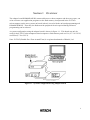
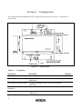
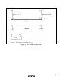
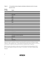
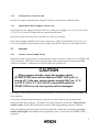
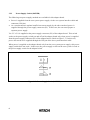
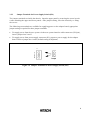
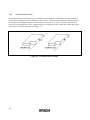
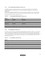
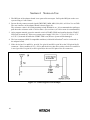
To all our customers Regarding the change of names mentioned in the document, such as Hitachi Electric and Hitachi XX, to Renesas Technology Corp. The semiconductor operations of Mitsubishi Electric and Hitachi were transferred to Renesas Technology Corporation on April 1st 2003. These operations include microcomputer, logic, analog and discrete devices, and memory chips other than DRAMs (flash memory, SRAMs etc.) Accordingly, although Hitachi, Hitachi, Ltd., Hitachi Semiconductors, and other Hitachi brand names are mentioned in the document, these names have in fact all been changed to Renesas Technology Corp. Thank you for your understanding. Except for our corporate trademark, logo and corporate statement, no changes whatsoever have been made to the contents of the document, and these changes do not constitute any alteration to the contents of the document itself. Renesas Technology Home Page: http://www.renesas.com Renesas Technology Corp. Customer Support Dept. April 1, 2003 F-ZTATTM Microcomputer On-Board Programming Adapter Board HS0008EASF4H User’s Manual HS0008EASF4HE(D) Cautions 1. Hitachi neither warrants nor grants licenses of any rights of Hitachi’s or any third party’s patent, copyright, trademark, or other intellectual property rights for information contained in this document. Hitachi bears no responsibility for problems that may arise with third party’s rights, including intellectual property rights, in connection with use of the information contained in this document. 2. Products and product specifications may be subject to change without notice. Confirm that you have received the latest product standards or specifications before final design, purchase or use. 3. Hitachi makes every attempt to ensure that its products are of high quality and reliability. However, contact Hitachi’s sales office before using the product in an application that demands especially high quality and reliability or where its failure or malfunction may directly threaten human life or cause risk of bodily injury, such as aerospace, aeronautics, nuclear power, combustion control, transportation, traffic, safety equipment or medical equipment for life support. 4. Design your application so that the product is used within the ranges guaranteed by Hitachi particularly for maximum rating, operating supply voltage range, heat radiation characteristics, installation conditions and other characteristics. Hitachi bears no responsibility for failure or damage when used beyond the guaranteed ranges. Even within the guaranteed ranges, consider normally foreseeable failure rates or failure modes in semiconductor devices and employ systemic measures such as fail-safes, so that the equipment incorporating Hitachi product does not cause bodily injury, fire or other consequential damage due to operation of the Hitachi product. 5. This product is not designed to be radiation resistant. 6. No one is permitted to reproduce or duplicate, in any form, the whole or part of this document without written approval from Hitachi. 7. Contact Hitachi’s sales office for any questions regarding this document or Hitachi semiconductor products. Contents Section 1 Overview..............................................................................................1 Section 2 Configuration.........................................................................................2 Section 3 Connectors, Switches, and LEDs...........................................................3 3.1 3.2 3.3 Connectors .......................................................................................................................................3 3.1.1 User Interface Connector (P1) ........................................................................................3 3.1.2 Serial Interface Connector (P2).......................................................................................7 3.1.3 Adapter Board Power-Supply Connector (P3).............................................................7 Switches............................................................................................................................................7 3.2.1 Transfer Switch (START/STOP)....................................................................................7 3.2.2 Power-Supply Switch (POWER)....................................................................................8 3.2.3 Jumper Terminals for Power-Supply Switch (JP1) .......................................................9 3.2.4 Circuit Protector (F1)........................................................................................................10 3.2.5 Control-Signal Enable/Disable Switches (S4)...............................................................11 3.2.6 Low (0)/High (1) Switches (S3).......................................................................................11 3.2.7 Vcc and PVcc Switches (S5 and S6)...............................................................................12 3.2.8 S3, S4, S5, and S6 Setting Examples ...............................................................................13 LEDs 13 3.3.1 START LED (START: Red)............................................................................................13 3.3.2 Power LED (POWER: Green)...........................................................................................13 Section 4 Notes on Use........................................................................................14 Section 5 Specifications ........................................................................................15 5.1 5.2 Input Voltage and Consumption Current ....................................................................................15 Write Processing.............................................................................................................................15 i Section 1 Overview The adapter board HS0008EASF4H, connected between a host computer and the user system, can write and erase user application programs on the flash memory incorporated in the F-ZTAT* microcomputer on the user system (on-board) when it is used with the on-board programming tool HS6400FWIW1SF. Therefore, the burden on the peripheral circuit required during on-board programming can be reduced. A system configuration using the adapter board is shown in figure 1.1. This board can only be used for the F-ZTAT microcomputers that incorporate a flash memory and use Vcc (2.7 V to 5.25 V) and PVcc (2.7 V to 5.25 V). Note: F-ZTAT (Flexible-Zero Turn Around Time) is a registered trademark of Hitachi, Ltd. Figure 1.1 System Configuration Using Adapter Board 1 Section 2 Configuration The configuration and components of the adapter board are shown in figure 2.1 and table 2.1, respectively. Figure 2.1 Adapter Board Table 2.1 Components Item Name Description Quantity Adapter board Main unit 1 Serial interface cable Connection between main unit and host computer (2000 mm) 1 User system interface cable Connection between main unit and user system (300 mm) 1 User system interface cable connector Connection between main unit and user system 1 Adapter board power cable Adapter board power supply (1000 mm) 1 2 Section 3 Connectors, Switches, and LEDs 3.1 Connectors This adapter board has connectors P1, P2, and P3. 3.1.1 User Interface Connector (P1) Observe the precautions listed below. Failure to do so will result in a FIRE HAZARD and will damage the user system and the adapter board or will result in PERSONAL INJURY. 1. Always switch OFF the adapter board and the user system before connecting or disconnecting ANY CABLES or PARTS. 2. Before connecting, always make sure that pin 1 on both sides are correctly aligned. 3. When disconnecting cables, take care not to put excessive stress on the cables. The signals required for writing to flash memory are shown in figures 3.1 and 3.2. Connect the adapter board and the user system using the user system interface cable provided (with an 20-pole connector on each end) and a user system interface cable connector (used for connecting the cable to the user system). The user system interface cable provided straight-matches the pins in the adapter board to those in the user system, as shown in figure 3.2. 3428-6002LCSC (manufactured by Sumitomo 3M Ltd.) is used as a user system interface cable connector. 3 Figure 3.1 Connector Pin Location 4 Figure 3.2 User System Interface Cable 5 Table 3.1 Correspondence between Signals and Numbers Indicated on the User System Interface Cable Number on Cable Signal 1 RES 2 GND 3 FWE/FWP 4 GND 5 MD0 6 GND 7 MD1 8 GND 9 IO0 10 GND 11 IO1 12 GND 13 IO2 14 GND 15 RXD (TXD for the user system) 16 GND 17 TXD (RXD for the user system) 18 VIN (Vcc) 19 NC 20 VIN (PVcc) If the device has Vcc and PVcc, provide Vcc (pin 18) and PVcc (pin 20) to the VIN pin of the P1 connector. If the condition is Vcc = PVcc and the device that does not have both Vcc and PVcc is used, provide Vcc (pin 18) or PVcc (pin 20) to the two VIN pins of the P1 connector. When the target microcomputer requires port control during on-board programming, connect necessary port signals. For details, refer to table 3.5 in section 3.2.8, S3, S4, S5, and S6 Setting Examples. 6 3.1.2 Serial Interface Connector (P2) Connect the adapter board and host computer using the serial interface cable provided. 3.1.3 Adapter Board Power-Supply Connector (P3) Supply power to the adapter board from the user system power supply (Vcc: 2.7 V to 5.25 V, PVcc: 2.7 V to 5.25 V) via the VIN pin of the user system interface cable. If the device does not use the PVcc, provide Vcc to the two VIN pins. If the current supply capability of the user system power supply is insufficient, power (Vcc 5 V ± 5%) can be supplied using a separate power supply from the P3 connector to the adapter board. 3.2 Switches 3.2.1 Transfer Switch (START/STOP) When this switch is pressed once, a programming control is initiated. In this case, the START LED (red) is turned on. When this switch is pressed again after program transfer, the programming control is terminated. At this time, the START LED (red) is turned off. CAUTION After program transfer, press the transfer switch (START/STOP) and confirm that the START LED (red) is turned off. If the user system power supply VIN (Vcc: 2.7 V to 5.25 V, PVcc: 2.7 V to 5.25 V) is turned off while the START LED is on, the user system will be damaged. For details on activating the on-board programming tool, refer to the On-Board Programming Tool User's Manual. Activate the on-board programming tool, and select the boot mode or user program mode displayed on the host computer. The hardware setting sequence is displayed. Then press the transfer switch. The START LED (red) is turned on and a programming control is initiated. After programming the flash memory in the selected mode, confirm the end message, press the transfer switch again, and complete the programming control. At this time, the START LED is turned off. 7 3.2.2 Power-Supply Switch (POWER) The following two power-supply methods are available for this adapter board. • Power is supplied from the user system power supply via the user system interface cable and connector (VIN pin). • As a countermeasure against insufficient current supply by the above method, power is supplied through the power-supply connector (P3). In this case, the user must prepare a separate power supply. Vcc 5 V ± 5% is supplied to the power-supply connector (P3) of the adapter board. This switch works as the power-supply switch (on and off) of the adapter board only when power is supplied from the power-supply connector (P3) of the adapter board. (Refer to figure 3.3.) In this case, power also needs to be supplied through the VIN pin of the user system interface cable. When power is supplied to the adapter board only from the user system power supply, this powersupply switch does not work. In this case, the power-supply switch on the user system is used as the power-supply switch for the adapter board. Figure 3.3 Power-Supply Switch (POWER) 8 3.2.3 Jumper Terminals for Power-Supply Switch (JP1) The jumper terminals are inside the chassis. Open the upper panel by removing the screw in each corner attaching the upper and lower panels. After jumper setting, close the chassis by re-fixing the screws. The following two methods are available for supplying power to the adapter board; appropriate jumper setting is required for these jumper terminals. • To supply power from the user system via the user system interface cable connector (VIN pin), insert a jumper into 2 and 3. • To supply power from power-supply connector (P3), prepare a power supply for the adapter board. Insert a jumper into 1 and 2 (default setting at shipment). Figure 3.4 Jumper Terminals for Power-Supply Switch (JP1) 9 3.2.4 Circuit Protector (F1) This adapter board is provided with a resumable circuit protector on the input section of the user system power supply to prevent damage to the system. If the circuit protector is turned off due to erroneous power-supply connection or excessive current (1 A or more), check the system, then return the circuit protector to the original state by pressing the switch in the hole with a thin pin or wire to activate the circuit protector (figure 3.5). Figure 3.5 Circuit Protector Setting 10 3.2.5 Control-Signal Enable/Disable Switches (S4) This adapter board is provided with switches so that each control signal can be enabled or disabled separately, as shown in table 3.2; the control-signal switches that are necessary to program the F-ZTAT microcomputer should be set to E. These switches are inside the case. Open the upper panel by removing the screw in each corner between the upper and lower panels. After switch setting, reclose the case and refasten the screws. Table 3.2 Control-Signal Enable/Disable Switches (S4) Signal E D FWE (S4-1) Enabled Disabled MD0 (S4-2) Enabled Disabled MD1 (S4-3) Enabled Disabled IO0 (S4-4) Enabled Disabled IO1 (S4-5) Enabled Disabled IO2 (S4-6) Enabled Disabled 3.2.6 Low (0)/High (1) Switches (S3) Level 0 or 1 can be selected by enabling the enable/disable switch (S4) (see table 3.2). Select 0 or 1 for the control signals according to the F-ZTAT microcomputer you are using (to program the FZTAT microcomputer). These switches are inside the case. Open the upper panel by removing the screw in each corner between the upper and lower panels. After switch setting, reclose the case and refasten the screws. Table 3.3 Low (0)/High (1) Switches (S3) Signal 0 1 FWE (S3-1) 0 1 MD0 (S3-2) 0 1 MD1 (S3-3) 0 1 IO0 (S3-4) 0 1 IO1 (S3-5) 0 1 IO2 (S3-6) 0 1 11 3.2.7 Vcc and PVcc Switches (S5 and S6) Select Vcc or PVcc level for the control signals according to the F-ZTAT microcomputer you are using (to program the F-ZTAT microcomputer). The Vcc or PVcc level can be selected by the switch settings of S5 and S6 (see table 3.4). The switches are inside the case. Open the upper panel by removing the screw in each corner between the upper and lower panels. After switch setting, reclose the case and refasten the screws. Table 3.4 Vcc and PVcc Switches (S5 and S6) Signal P V FWE (S5-1) PVcc Vcc MD0 (S5-2) PVcc Vcc MD1 (S5-3) PVcc Vcc IO0 (S5-4) PVcc Vcc IO1 (S6-1) PVcc Vcc IO2 (S6-2) PVcc Vcc 12 3.2.8 S3, S4, S5, and S6 Setting Examples Table 3.5 shows examples of S3 to S6 switch settings for on-board programming in boot mode. When using an F-ZTAT microcomputer that is not listed in table 3.5, refer to the corresponding hardware manual. Table 3.5 S3, S4, S5, and S6 Setting Examples HS0008EASF4H SH7055F P1 Connector Signal MCU Signal S4 S3 S5 and S6 VIN (Vcc) Vcc *1 *1 *1 VIN (PVcc) PVcc2 *1 *1 *1 GND Vss *1 *1 *1 RES RES *1 *1 *1 TXD RXD *1 *1 *1 RXD TXD *1 *1 *1 FWE/FWP FWE E 1 C (S5-1) MD0 MD1 E 0 P (S5-2) MD1 MD2 E 1 P (S5-3) IO0 — *3 D *2 *2 IO1 —*3 D *2 *2 IO2 —*3 D *2 *2 Notes: 1. The P1 connector signals and MCU signals on the user system must always be connected regardless of the S3, S4, S5, and S6 settings. 2. Either setting is available. 3. Need not be connected. 3.3 LEDs 3.3.1 START LED (START: Red) This LED is turned on or off when the transfer switch (START/STOP) is pressed. 3.3.2 Power LED (POWER: Green) This LED is on while the user system power supply VIN (Vcc: 2.7 V to 5.25 V, PVcc: 2.7 V to 5.25 V) or the power supply Vcc (5 V ± 5%) dedicated to the adapter board is supplied. 13 Section 4 Notes on Use 1. The RES pin of the adapter board is an open-collector output. Pull up the RES pin on the user system using a 1-kΩ resistor. 2. Do not directly connect control signals FWP/FWE, MD0, MD1, IO0, IO1, or IO2 to Vcc or GND. The user interface of the adapter board is shown figure 4.1. The resistance value is 20 Ω when analog switch HC4066 is on. It is recommended to pull up or pull down the resistance with 4.7-kΩ or more. (For revision A, 47 kΩ or more is recommended.) 3. After program transfer, press the transfer switch (START/STOP) and confirm that the START LED (red) is turned off. If the user system power supply VIN (Vcc: 2.7 V to 5.25 V, PVcc: 2.7 V to 5.25 V) is turned off while the START LED is on, the user system will be damaged. 4. The host computer (DOS/V compatible machines) with built-in Pentium can be connected to the adapter board. 5. If the device has Vcc and PVcc, provide Vcc (pin 18) and PVcc (pin 20) to the VIN pin of the P1 connector. If the condition is Vcc = PVcc and the device that does not have both Vcc and PVcc is used, provide Vcc (pin 18) or PVcc (pin 20) to the two VIN pins of the P1 connector. Figure 4.1 Control-Signal Circuit Example 14 Section 5 Specifications 5.1 Input Voltage and Consumption Current • Power-supply input (VIN) from the user interface connector (Vcc: 2.7 V to 5.25 V, PVcc: 2.7 V to 5.25 V) • Power-supply input (Vcc) from the P3 connector of the adapter board: 5 V ± 5% • Consumption current: 200 mA at 5 V or 330 mA at 3 V 5.2 Write Processing 1. When the transfer switch is pressed, the RES signal is held to the low level for 500 ms. 2. After 10 ms of the falling edge of the RES signal, 2.7- to 5.25-V application to the FWE/FWP pin starts or stops (figure 5.1). Figure 5.1 Reset Signal, 2.7- to 5.25-V Application, and Stop Timing 15