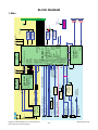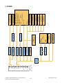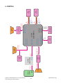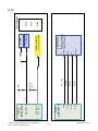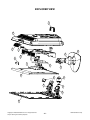
1
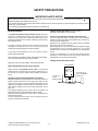
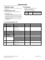
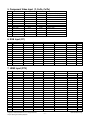
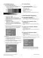
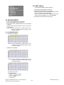
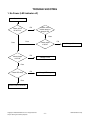
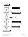
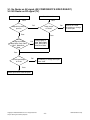
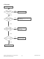
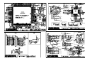
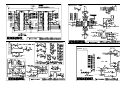
CONTENTS
CONTENTS .............................................................................................. 2
SAFETY PRECAUTIONS ......................................................................... 3
SPECIFICATION ....................................................................................... 6
ADJUSTMENT INSTRUCTION ................................................................ 8
TROUBLE SHOOTING ........................................................................... 11
BLOCK DIAGRAM.................................................................................. 14
EXPLODED VIEW .................................................................................. 22
REPLACEMENT PARTS LIST ............................................................... 24
SVC. SHEET ...............................................................................................
Copyright © 2008 LG Electronics. Inc. All right reserved.
Only for training and service purposes
-2-
LGE Internal Use Only
SAFETY PRECAUTIONS
IMPORTANT SAFETY NOTICE
Many electrical and mechanical parts in this chassis have special safety-related characteristics. These parts are identified by
in the
Schematic Diagram and Replacement Parts List.
It is essential that these special safety parts should be replaced with the same components as recommended in this manual to prevent
Shock, Fire, or other Hazards.
Do not modify the original design without permission of manufacturer.
Leakage Current Hot Check (See below Figure)
Plug the AC cord directly into the AC outlet.
General Guidance
An isolation Transformer should always be used during the
servicing of a receiver whose chassis is not isolated from the AC
power line. Use a transformer of adequate power rating as this
protects the technician from accidents resulting in personal injury
from electrical shocks.
It will also protect the receiver and it's components from being
damaged by accidental shorts of the circuitry that may be
inadvertently introduced during the service operation.
If any fuse (or Fusible Resistor) in this TV receiver is blown,
replace it with the specified.
When replacing a high wattage resistor (Oxide Metal Film Resistor,
over 1W), keep the resistor 10mm away from PCB.
Do not use a line Isolation Transformer during this check.
Connect 1.5K/10watt resistor in parallel with a 0.15uF capacitor
between a known good earth ground (Water Pipe, Conduit, etc.)
and the exposed metallic parts.
Measure the AC voltage across the resistor using AC voltmeter
with 1000 ohms/volt or more sensitivity.
Reverse plug the AC cord into the AC outlet and repeat AC voltage
measurements for each exposed metallic part. Any voltage
measured must not exceed 0.75 volt RMS which is corresponds to
0.5mA.
In case any measurement is out of the limits specified, there is
possibility of shock hazard and the set must be checked and
repaired before it is returned to the customer.
Leakage Current Hot Check circuit
Keep wires away from high voltage or high temperature parts.
AC Volt-meter
Before returning the receiver to the customer,
always perform an AC leakage current check on the exposed
metallic parts of the cabinet, such as antennas, terminals, etc., to
be sure the set is safe to operate without damage of electrical
shock.
Leakage Current Cold Check(Antenna Cold Check)
With the instrument AC plug removed from AC source, connect an
electrical jumper across the two AC plug prongs. Place the AC
switch in the on position, connect one lead of ohm-meter to the AC
plug prongs tied together and touch other ohm-meter lead in turn to
each exposed metallic parts such as antenna terminals, phone
jacks, etc.
If the exposed metallic part has a return path to the chassis, the
measured resistance should be between 1MΩ and 5.2MΩ.
When the exposed metal has no return path to the chassis the
reading must be infinite.
An other abnormality exists that must be corrected before the
receiver is returned to the customer.
Copyright © 2008 LG Electronics. Inc. All right reserved.
Only for training and service purposes
-3-
To Instrument's
exposed
METALLIC PARTS
Good Earth Ground
such as WATER PIPE,
CONDUIT etc.
0.15uF
1.5 Kohm/10W
LGE Internal Use Only
SERVICING PRECAUTIONS
CAUTION: Before servicing receivers covered by this service
manual and its supplements and addenda, read and follow the
SAFETY PRECAUTIONS on page 3 of this publication.
NOTE: If unforeseen circumstances create conflict between the
following servicing precautions and any of the safety precautions on
page 3 of this publication, always follow the safety precautions.
Remember: Safety First.
General Servicing Precautions
1. Always unplug the receiver AC power cord from the AC power
source before;
a. Removing or reinstalling any component, circuit board
module or any other receiver assembly.
b. Disconnecting or reconnecting any receiver electrical plug or
other electrical connection.
c. Connecting a test substitute in parallel with an electrolytic
capacitor in the receiver.
CAUTION: A wrong part substitution or incorrect polarity
installation of electrolytic capacitors may result in an
explosion hazard.
2. Test high voltage only by measuring it with an appropriate high
voltage meter or other voltage measuring device (DVM,
FETVOM, etc) equipped with a suitable high voltage probe.
Do not test high voltage by "drawing an arc".
3. Do not spray chemicals on or near this receiver or any of its
assemblies.
4. Unless specified otherwise in this service manual, clean
electrical contacts only by applying the following mixture to the
contacts with a pipe cleaner, cotton-tipped stick or comparable
non-abrasive applicator; 10% (by volume) Acetone and 90% (by
volume) isopropyl alcohol (90%-99% strength)
CAUTION: This is a flammable mixture.
Unless specified otherwise in this service manual, lubrication of
contacts in not required.
5. Do not defeat any plug/socket B+ voltage interlocks with which
receivers covered by this service manual might be equipped.
6. Do not apply AC power to this instrument and/or any of its
electrical assemblies unless all solid-state device heat sinks are
correctly installed.
7. Always connect the test receiver ground lead to the receiver
chassis ground before connecting the test receiver positive
lead.
Always remove the test receiver ground lead last.
8. Use with this receiver only the test fixtures specified in this
service manual.
CAUTION: Do not connect the test fixture ground strap to any
heat sink in this receiver.
Electrostatically Sensitive (ES) Devices
Some semiconductor (solid-state) devices can be damaged easily
by static electricity. Such components commonly are called
Electrostatically Sensitive (ES) Devices. Examples of typical ES
devices are integrated circuits and some field-effect transistors and
semiconductor "chip" components. The following techniques
should be used to help reduce the incidence of component
damage caused by static by static electricity.
1. Immediately before handling any semiconductor component or
semiconductor-equipped assembly, drain off any electrostatic
charge on your body by touching a known earth ground.
Alternatively, obtain and wear a commercially available
discharging wrist strap device, which should be removed to
prevent potential shock reasons prior to applying power to the
Copyright © 2008 LG Electronics. Inc. All right reserved.
Only for training and service purposes
unit under test.
2. After removing an electrical assembly equipped with ES
devices, place the assembly on a conductive surface such as
aluminum foil, to prevent electrostatic charge buildup or
exposure of the assembly.
3. Use only a grounded-tip soldering iron to solder or unsolder ES
devices.
4. Use only an anti-static type solder removal device. Some solder
removal devices not classified as "anti-static" can generate
electrical charges sufficient to damage ES devices.
5. Do not use freon-propelled chemicals. These can generate
electrical charges sufficient to damage ES devices.
6. Do not remove a replacement ES device from its protective
package until immediately before you are ready to install it.
(Most replacement ES devices are packaged with leads
electrically shorted together by conductive foam, aluminum foil
or comparable conductive material).
7. Immediately before removing the protective material from the
leads of a replacement ES device, touch the protective material
to the chassis or circuit assembly into which the device will be
installed.
CAUTION: Be sure no power is applied to the chassis or circuit,
and observe all other safety precautions.
8. Minimize bodily motions when handling unpackaged
replacement ES devices. (Otherwise harmless motion such as
the brushing together of your clothes fabric or the lifting of your
foot from a carpeted floor can generate static electricity
sufficient to damage an ES device.)
General Soldering Guidelines
1. Use a grounded-tip, low-wattage soldering iron and appropriate
tip size and shape that will maintain tip temperature within the
range or 500°F to 600°F.
2. Use an appropriate gauge of RMA resin-core solder composed
of 60 parts tin/40 parts lead.
3. Keep the soldering iron tip clean and well tinned.
4. Thoroughly clean the surfaces to be soldered. Use a mall wirebristle (0.5 inch, or 1.25cm) brush with a metal handle.
Do not use freon-propelled spray-on cleaners.
5. Use the following unsoldering technique
a. Allow the soldering iron tip to reach normal temperature.
(500°F to 600°F)
b. Heat the component lead until the solder melts.
c. Quickly draw the melted solder with an anti-static, suctiontype solder removal device or with solder braid.
CAUTION: Work quickly to avoid overheating the circuit
board printed foil.
6. Use the following soldering technique.
a. Allow the soldering iron tip to reach a normal temperature
(500°F to 600°F)
b. First, hold the soldering iron tip and solder the strand against
the component lead until the solder melts.
c. Quickly move the soldering iron tip to the junction of the
component lead and the printed circuit foil, and hold it there
only until the solder flows onto and around both the
component lead and the foil.
CAUTION: Work quickly to avoid overheating the circuit
board printed foil.
d. Closely inspect the solder area and remove any excess or
splashed solder with a small wire-bristle brush.
-4-
LGE Internal Use Only
IC Remove/Replacement
Some chassis circuit boards have slotted holes (oblong) through
which the IC leads are inserted and then bent flat against the
circuit foil. When holes are the slotted type, the following technique
should be used to remove and replace the IC. When working with
boards using the familiar round hole, use the standard technique
as outlined in paragraphs 5 and 6 above.
Removal
1. Desolder and straighten each IC lead in one operation by gently
prying up on the lead with the soldering iron tip as the solder
melts.
2. Draw away the melted solder with an anti-static suction-type
solder removal device (or with solder braid) before removing the
IC.
Replacement
1. Carefully insert the replacement IC in the circuit board.
2. Carefully bend each IC lead against the circuit foil pad and
solder it.
3. Clean the soldered areas with a small wire-bristle brush.
(It is not necessary to reapply acrylic coating to the areas).
"Small-Signal" Discrete Transistor
Removal/Replacement
1. Remove the defective transistor by clipping its leads as close as
possible to the component body.
2. Bend into a "U" shape the end of each of three leads remaining
on the circuit board.
3. Bend into a "U" shape the replacement transistor leads.
4. Connect the replacement transistor leads to the corresponding
leads extending from the circuit board and crimp the "U" with
long nose pliers to insure metal to metal contact then solder
each connection.
Power Output, Transistor Device
Removal/Replacement
1. Heat and remove all solder from around the transistor leads.
2. Remove the heat sink mounting screw (if so equipped).
3. Carefully remove the transistor from the heat sink of the circuit
board.
4. Insert new transistor in the circuit board.
5. Solder each transistor lead, and clip off excess lead.
6. Replace heat sink.
Circuit Board Foil Repair
Excessive heat applied to the copper foil of any printed circuit
board will weaken the adhesive that bonds the foil to the circuit
board causing the foil to separate from or "lift-off" the board. The
following guidelines and procedures should be followed whenever
this condition is encountered.
At IC Connections
To repair a defective copper pattern at IC connections use the
following procedure to install a jumper wire on the copper pattern
side of the circuit board. (Use this technique only on IC
connections).
1. Carefully remove the damaged copper pattern with a sharp
knife. (Remove only as much copper as absolutely necessary).
2. carefully scratch away the solder resist and acrylic coating (if
used) from the end of the remaining copper pattern.
3. Bend a small "U" in one end of a small gauge jumper wire and
carefully crimp it around the IC pin. Solder the IC connection.
4. Route the jumper wire along the path of the out-away copper
pattern and let it overlap the previously scraped end of the good
copper pattern. Solder the overlapped area and clip off any
excess jumper wire.
At Other Connections
Use the following technique to repair the defective copper pattern
at connections other than IC Pins. This technique involves the
installation of a jumper wire on the component side of the circuit
board.
1. Remove the defective copper pattern with a sharp knife.
Remove at least 1/4 inch of copper, to ensure that a hazardous
condition will not exist if the jumper wire opens.
2. Trace along the copper pattern from both sides of the pattern
break and locate the nearest component that is directly
connected to the affected copper pattern.
3. Connect insulated 20-gauge jumper wire from the lead of the
nearest component on one side of the pattern break to the lead
of the nearest component on the other side.
Carefully crimp and solder the connections.
CAUTION: Be sure the insulated jumper wire is dressed so the
it does not touch components or sharp edges.
Diode Removal/Replacement
1. Remove defective diode by clipping its leads as close as
possible to diode body.
2. Bend the two remaining leads perpendicular y to the circuit
board.
3. Observing diode polarity, wrap each lead of the new diode
around the corresponding lead on the circuit board.
4. Securely crimp each connection and solder it.
5. Inspect (on the circuit board copper side) the solder joints of
the two "original" leads. If they are not shiny, reheat them and if
necessary, apply additional solder.
Fuse and Conventional Resistor
Removal/Replacement
1. Clip each fuse or resistor lead at top of the circuit board hollow
stake.
2. Securely crimp the leads of replacement component around
notch at stake top.
3. Solder the connections.
CAUTION: Maintain original spacing between the replaced
component and adjacent components and the circuit board to
prevent excessive component temperatures.
Copyright © 2008 LG Electronics. Inc. All right reserved.
Only for training and service purposes
-5-
LGE Internal Use Only
SPECIFICATION
NOTE : Specifications and others are subject to change without notice for improvement.
1. Application range
3. Test method
This specification is applied to the 19”/ 22” Wide LCD TV used
LA85C chassis.
2. Requirement for Test
1) Performance: LGE TV test method followed
2) Demanded other specification
- Safety: UL, CSA, IEC specification
- EMC: FCC, ICES, IEC specification
Model
Each part is tested as below without special appointment.
19LG30-UA
1) Temperature: 20±5ºC
2) Relative Humidity: 65±10%
3) Power Voltage : Standard input voltage(100-240V~, 50/60Hz)
* Standard Voltage of each product is marked by models
4) Specification and performance of each parts are followed
each drawing and specification by part number in
accordance with BOM.
5) The receiver must be operated for about 20 minutes prior to
the adjustment.
Market
Appliance
Central America Safety : UL1492, CSA C22.2.No.1
22LG30-UA
EMC : FCC Class B, IEC Class B
4. General Specification(TV)
No
Item
Specification
Option
1
Receivable System
ATSC/64 & 256 QAM/ NTSC-M
2
Available Channel
VHF : 02 ~ 13
Remark
USA only
UHF : 14 ~ 69
DTV : 02 ~ 69
CATV : 01 ~ 135
CADTV : 01 ~ 135
3
Input Voltage
100-240V~, 50/60Hz
4
Market
North and Central America
5
Screen Size
19/22 Inch
6
Aspect Ratio
16:9
7
Tuning System
FS
8
LCD Module
LM190WX1 (1440*900)
Wide, LPL
Not applied.
M190A1-L07 (1440*900)
Wide, CHI MEI
19LG30-UA (07.11.05)
LM220WE1 (1680*1050)
Wide, LPL
22LG30-UA
M220Z1-L01 (1680*1050)
Wide, CHI MEI
Not applied.
9
Operating Environment
Temp : 0 ~ 40 deg
10
Storage Environment
Temp : -20 ~ 60 deg
Humidity : ~ 80 %
Humidity : 0 ~ 85 %
Copyright © 2008 LG Electronics. Inc. All right reserved.
Only for training and service purposes
-6-
LGE Internal Use Only
5. Component Video Input (Y, CB/PB, CR/PR)
No
H-freq(kHz)
V-freq.(kHz)
1
2
720*480
720*480
Resolution
15.73
15.73
59.94
60.00
SDTV, DVD 480I(525I)
SDTV, DVD 480I(525I)
Proposed
3
4
720*480
720*480
31.47
31.50
59.94
60.00
SDTV 480P
SDTV 480P
5
1280*720
44.96
59.94
HDTV 720P
6
7
1280*720
1920*1080
45.00
33.72
60.00
59.94
HDTV 720P
HDTV 1080I
8
9
1920*1080
1920*1080
33.75
27
60.00
24
HDTV 1080I
HDTV 1080P
10
1920*1080
33.75
30
HDTV 1080P
11
12
1920*1080
1920*1080
67.43
67.5
59.94
60
HDTV 1080P
HDTV 1080P
6. RGB Input (PC)
No
Resolution
PC
H-freq(kHz)
V-freq.(Hz)
Pixel clock(MHz)
Remark
Proposed
DDC
1
2
640*350
720*400
31.469
31.469
70.08
70.08
25.17
28.32
DOS
DOS
O
3
640*480
31.469
59.94
25.17
VESA(VGA)
O
4
5
800*600
1024*768
37.879
48.363
60.31
60.00
40.00
65.00
VESA(SVGA)
VESA(XGA)
O
O
6
7
1280*768
1360*768
47.776
47.712
59.87
60.01
79.50
85.50
VESA(WXGA)
VESA(WXGA)
O
O
8
9
1440*900
1400*1050
55.5
64.744
59.90
59.948
88.750
101.00
22LG30-UA only
WXGA
WSXGA
10
1680*1050
62.290
59.954
146.25
22LG30-UA only
WSXGA
Remark
7. HDMI input (DTV)
No
Resolution
PC
H-freq(kHz)
V-freq.(Hz)
Pixel clock(MHz)
1
640*480
31.469
59.94
25.17
VESA(VGA)
O
2
3
800*600
1024*768
37.879
48.363
60.31
60.00
40.00
65.00
VESA(SVGA)
VESA(XGA)
O
O
4
5
1280*768
1360*768
47.776
47.720
59.87
59.799
79.50
84.75
CVT(WXGA)
CVT(WXGA)
O
O
6
1440*900
55.5
59.90
88.750
19/22LG30-UA only
WXGA
7
8
1400*1050
1680*1050
64.744
65.290
59.948
59.954
101.00
146.25
22LG30-UA only
22LG30-UA only
WSXGA
WSXGA
1
DTV
720*480
31.469
59.94
27.00
SDTV 480P
2
3
720*480
1280*720
31.500
44.96
60.00
59.94
27.03
74.17
SDTV 480P
HDTV 720P
4
1280*720
45.00
60.00
74.25
HDTV 720P
5
6
1920*1080
1920*1080
33.72
33.75
59.94
60.00
74.17
74.25
HDTV 1080I
HDTV 1080I
7
8
1920*1080
1920*1080
27
33.75
24.00
30.00
74.25
74.25
HDTV 1080P
HDTV 1080P
9
1920*1080
67.43
59.94
148.35
HDTV 1080P
10
1920*1080
67.5
60.00
148.50
HDTV 1080P
Copyright © 2008 LG Electronics. Inc. All right reserved.
Only for training and service purposes
-7-
Proposed
DDC
LGE Internal Use Only
ADJUSTMENT INSTRUCTION
1. Application Range
(5)
This specification sheet is applied for all of the LCD TV with
LA85C chassis.
filexxx.bin
(7) ........ OK
2. Specification
1) The adjustment is according to the order which is
designated and which must be followed, according to the
plan which can be changed only on agreeing.
2) Power Adjustment : 100-240V~, 50/60Hz
3) Magnetic Field Condition : Nil.
4) Input signal Unit : Product Specification Standard
5) Reserve after operation : Above 30 Minutes
6) Adjustment equipments: Color Analyzer(CA-210 or CA110), Pattern Generator (MSPG-925L or Equivalent), DDC
Adjustment Jig equipment, SVC remote control
(6)
3.2. ADC Process
3.2.1. PC input ADC
3. Main PCB check process
* APC - After Manual-Insult, executing APC
3.1. Software download
1) Execute ISP program “Mstar ISP Utility” and then click
“Config” tab.
2) Set as below, and then click “Auto Detect” and check “OK”
message. If display “Error”, Check connect computer, jig,
and set.
3) Click “Connect” tab. If display “Can’t”, Check connect
computer, jig, and set.
(1)
(3)
<Adjustment pattern (PC)>
Please Check Speed :
To us speed between from 200 KHz
to 400 KHz
(2)
(1) Auto RGB Gain/Offset Adjustment
1) Convert to PC in Input-source
I2C COMMAND:0xF4(SELECT INPUT) 0x00 0x60(RGB)
cf. 0x10(TV), 0x20(AV), 0x40(COMPONENT),
0x60(RGB), 0x90(HDMI)
2) Signal equipment displays
Output Voltage : 700 mVp-p
Impress Resolution XGA (1024x 768 @ 60Hz)
Model : 60 in Pattern Generator
Pattern : 29 in Pattern Generator (MSPG-925 Series)
[gray pattern that left & right is black and center is
white signal (Refer below picture)].
3) Adjust by commanding AUTO_COLOR _ADJUST
(0xF1) 0x00 0x02 instruction.
OK
4) Click “Read” tab, and then load download file(XXXX.bin) by
clicking “Read”.
(4)
* Manual ADC process using Service Remote control. After
enter Service Mode by pushing “ADJ” key, execute “Autoadjust” by pushing “G” key at “0. ADC CALIBRATION”.
filexxx.bin
EZ ADJUST
0. ADC CALIBRATION
: RGB
1. ADC ADJUST
2. SUB B/C ADJUST
3. W/B ADJUST
4. WHITE PATTERN
: OFF
5. 2HOUR OFF
: ON
6. OAD
7. UART DOWNLOAD
8. FACTORY MODE
: ON
9. DEBUG MODE
: OFF
5) Click “Auto” tab and set as below
6) click “Run”.
7) After downloading, check “OK” message.
Copyright © 2008 LG Electronics. Inc. All right reserved.
Only for training and service purposes
(2) Confirmation
1) We confirm whether “0xB6” address of EEPROM
“0xA2” is “0xAA” or not.
2) If “0xB6(RGB)” address of EEPROM “0xB2” isn’t
“0xAA”, we adjust once more.
3) We can confirm the ADC values from “0xB0~0xB5
(RGB)” addresses in a page “0xA2”
-8-
LGE Internal Use Only
3.2.2. COMPONENT input ADC
3.3. Function Check
(1) Component Gain/Offset Adjustment
1) Convert to Component in Input-source
I2C command : 0xF4(Select input) 0x00 0x40(Component)
cf. 0x10(TV), 0x20(AV), 0x40(COMPONENT),
0x60(RGB), 0x90(HDMI)
3.3.1. Check display and sound
- Check Input and Signal items. (cf. work instructions)
1) TV
2) AV (CVBS/ S-Video)
3) COMPONENT (480i)
4) RGB (PC : 1024 x 768 @ 60hz)
5) HDMI
6) PC Audio In and H/P Out
* Display and Sound check is executed by Remote control.
<Adjustment pattern (COMPONENT)>
2) Signal equipment displays
Impress Resolution 480i
MODEL : 209 in Pattern Generator(480i Mode)
PATTERN : 08 in Pattern Generator(MSPG-925 Series)
3) Adjust by commanding AUTO_COLOR_ADJUST (0xF1)
0x00 0x02 instruction.
4) Signal equipment display
-Impress Resolution : 1080i
- MODEL: 223 in Pattern Generator(1080i Mode)
- PATTERN: 08 in Pattern generator(MAPG-925 series)
5) Adjust by commanding AUTO_COLOR ADJUST(0xF1)
0x00 0x02 instruction.
* Manual ADC process using Service Remote control. After
enter Service Mode by pushing “ADJ” key, execute “Autoadjust” by pushing “G” key at “0. ADC CALIBRATION”.
EZ ADJUST
0. ADC CALIBRATION : COMPONENT
1. ADC ADJUST
2. SUB B/C ADJUST
3. W/B ADJUST
4. WHITE PATTERN
: OFF
5. 2HOUR OFF
: ON
6. OAD
7. UART DOWNLOAD
8. FACTORY MODE
: ON
9. DEBUG MODE
: OFF
4. Total Assembly line process
4.1. Adjustment Preparation
1) Heat-run above 30 minutes in RF no signal.
2) 15 Pin D-sub jack is connected to the auto W/B equipment.
4.2. Adjust color coordinate of Cool
1) Set Input to RGB.
2) Set Temperature : Cool
3) Adjust x=0.285±0.005, y=0.293±0.005 (9300ºK±1000ºK) or
not.
4.3. Adjust color coordinate of Medium
1) Set Input to RGB.
2) Set Temperature : Medium
3) Adjust x=0.295±0.005, y=0.305±0.005 (8000ºK±1000ºK) or
not.
4.4. Adjust color coordinate of Warm
1) Set Input to RGB.
2) Set Temperature : Warm
3) Adjust x=0.313±0.005, y=0.329±0.005 (8000ºK±1000ºK) or
not.
(2) Confirmation
1) We confirm whether “0xBF(480i)/0xC8(1080i)” address
of EEPROM “0xA2” is “0xAA” or not.
2) If “0xBF(480i)/0xC8(1080i)” address of EEPROM “0xA2”
isn’t “0xAA”, we adjust once more.
3) We can confirm the ADC values from “0xB9~0xBE(480i)/
0xC2~(1080i)” addresses in a page “0xA2”.
* Manual ADC Confirmation using Service Remocon. After
enter Service Mode by pushing “INSTART” key.
MODEL : 22LG30_UA_UA/LPL_LM220WT7
S/W VER : 3.00.1
UTT : 6
ADC CAL.
RGB : OK
YPbPr(SD) : OK
YPbPr(HD) : OK
0. STEREO DETECT
1. SYNC LEVEL
2. DTV SNR
3. SCREEN MUTE
4. POWER OFF HISTORY
Copyright © 2008 LG Electronics. Inc. All right reserved.
Only for training and service purposes
* Manual ADC Confirmation using Service Remocon. After
enter Service Mode by pushing “INSTART” key.
EZ ADJUST
0. ADC CALIBRATION : RGB
1. ADC ADJUST
2. SUB B/C ADJUST
3. W/B ADJUST
4. WHITE PATTERN
: OFF
5. 2HOUR OFF
: ON
6. OAD
7. UART DOWNLOAD
8. FACTORY MOD
: ON
9. DEBUG MODE
: OFF
* Adjust “R/G/B - GAIN” by pushing “F”, “G” key at “Cool”
* Adjust “R/G/B - GAIN” by pushing “F”, “G” key at “Medium”
* Adjust “R/G/B - GAIN” by pushing “F”, “G” key at “Warm”
-9-
LGE Internal Use Only
4.6. HDCP setting
W/B ADJUST
0. MODE : RGB
1. WHITE PATTERN : White
2. TEMPERATURE : Cool
3. R - GAIN : 128
4. G - GAIN : 128
5. B - GAIN : 128
6. R – OFFSET : 128
7. G – OFFSET : 128
8. B – OFFSET : 128
9. RESET
(High-Bandwidth Digital Contents Protection)
1) Connect D-sub Signal Cable to D-Sub Jack.
2) Input HDCP key with HDCP-key- in-program.
3) HDCP Key value is stored on EEPROM(AT24C512) which
is 80~A1 addresses of 0xA0~0xA2 page
4) AC off/ on and on HDCP button of MSPG925 and confirm
whether picture is displayed or not of using MSPG925
5) HDCP Key value is different among the sets.
4.5. DDC EDID WRITE
1) Connect D-sub Signal Cable to D-Sub Jack.
2) Connect HDMI Signal Cable to HDMI Jack.
3) Write EDID DATA to EEPROM (24C02) by using DDC2B
protocol.
4) Check whether written EDID data is correct or not. (Refer to
Product spec).
5) Remark : A week manufacture in address 0x10 can be
changed. And thus Checksum (Address: 0x7F)
can be also changed.
4.5.1. 19LG30 EDID DATA
(1) ANALOG DATA 128Byte
- Remark: A week manufacture in address 0x10 can be
changed. And thus Checksum (Address: 0x7F)
can be also changed.
(2) DIGITAL DATA 256Byte
- Remark: A week manufacture in address 0x10 can be
changed. And thus Checksum (Address: 0x7F)
can be also changed.
1) All Data : HEXA Value
2) Changeable Data :
*: Serial No : Controlled / Data:01
**: Month : Controlled / Data:00
***:Year : Controlled
****:Check sum
Copyright © 2008 LG Electronics. Inc. All right reserved.
Only for training and service purposes
- 10 -
LGE Internal Use Only
TROUBLE SHOOTING
1. No Power (LED indicator off)
Start check
Fail
Check 15V or
5V of P701.
Check short
of Main board or
change LIPS.
Pass
Pass
Pass
Check Output
of IC705.
Check output
of Q701.
Fail
Change Q701.
Fail
Change IC705.
Pass
Fail
Check LED Assy.
Change LED Assy.
Pass
Check P304 & Connector.
Copyright © 2008 LG Electronics. Inc. All right reserved.
Only for training and service purposes
- 11 -
LGE Internal Use Only
2. No RASTER
Start check
Check LED status
On Display Unit.
Fail
Repeat No power (1) PROCESS.
Pass
Check
IC700, IC702,
IC703, IC704, IC705, IC706,
IC708, IC709,
IC710.
Fail
Change IC700, IC702, IC703, IC704,
IC705, IC706, IC708, IC709, IC710.
Pass
Check input/output
of IC00.
Fail
Change IC100
Pass
Check the
inverter connector or
inverter.
Fail
Change inverter connector or inverter
Pass
Check LVDS cable
or module.
Fail
Change LVDS cable or module.
Pass
Check input source cable & jack.
Copyright © 2008 LG Electronics. Inc. All right reserved.
Only for training and service purposes
- 12 -
LGE Internal Use Only
3-1. No Raster on AV signal (AV/ COMPONENT/ S-VIDEO RGB-PC)
3-2. NO Raster on RF signal (TV)
Start Check 3-1
Start Check 3-2
Pass
Pass
Fail
Repeat No power(1)
process.
Check output
of TU400.
Pass
Check
the signal of R622,
R623, R681, R615, R616,
R617, R640,R641,
R642.
Fail
Check 5V of TU400.
Re-Soldering or change
the defect part.
Pass
Fail
Change signal of
R622, R623, R681,
R615, R616, R617,
R640,R641,R642.
Pass
Check input/output
of IC100.
Fail
Re-soldering or change defect part.
Check X100.
Pass
Check input source cable and jack.
Copyright © 2008 LG Electronics. Inc. All right reserved.
Only for training and service purposes
- 13 -
LGE Internal Use Only
4. No sound
Start Check
Check the input
Source.
Fail
Change source input.
Pass
Check input/Output
of IC100.
Fail
Re-soldering or change the defect part.
Check the X100.
Fail
Re-soldering or change
the defect part.
Pass
Check the input/
output of IC500.
Pass
Fail
Check the Speaker.
Change the speaker.
Pass
Check the Speaker wire.
Copyright © 2008 LG Electronics. Inc. All right reserved.
Only for training and service purposes
- 14 -
LGE Internal Use Only
[3]
[N:11]
[P:10]
SCL[8]
[12]
Copyright © 2008 LG Electronics. Inc. All right reserved.
Only for training and service purposes
1.0Vp-p
96dBuV
[16]
[15]
SDA[7]
- 15 -
EAG31022001
USB(SVC only)
6630G00001A
RS232C(SVC only)
6612F00099A
PC Audio IN
6630G70016A
PC(VGA)
6612J10031C
Tx_Out
IF-P
IF-N
SIF
TPA6110A20
Tx/Rx
EAN41348201
ST-5V
R232C_Tx
R232C_Rx
ST-5V
HPDCTRL[12]
PC IN
Comp1
DDC_SDA/UART_TX12V
DDC_SCL/UART_RX
HP_L/r[70,71]
TXCLK-[2]
TXCLK+[3]
IN1
IN1
SIFP0
SIFM0
TUNER_CVBS
VCOM0
1.25V 3.3V
LVDS(8Bit)
HY5DU561622F
256M (DDR)
HY5DU561622F
256M (DDR)
2.5V
VDD_DDR
3.3V
AVDD_DVI
OUT_P_R[8]
OUT_N_R[14]
OUT_P_L[35]
OUT_N_L[29]
(YDA148-EZ)
EAN40130001
D-AMP
MUTE[6]
Audio_R
IN_R[5]
HP_DET[37]
IN_L[38]
Audio_L
LGE1854C
L OUT
R OUT
CVBS1[42]
AUL_IN0[54]
AUR_IN[55]
AV1_SW[111]
SV_C0[38]
SV_Y0[39]
MSTAR
S_SW[82]
EAN37156404SCL_EEPROM[136]
SDA_EEPROM[135]
B_TX0-[4] Air : 8VSB
EEPROM(512K)
EEPROM(512K)
B_TX0+[5]
24C512
Cable : 256/64QAM
24C512
G_TX1-[7]
•RGB/YPbYr*2
G_TX1[8]
0IMMRAL025A
R_TX2-[10] •CVBS*3
SPI_CK[129]
R_TX2+[11]
SPI_DI[130]
PB_IN[26] •YC*2
Flash
Flash(64M)
(64M)
SPI_DO[131]
SOY[29]
•L/R-IN*3
S25FL064A
S25FL064A
SPI_CZ[132]
Y_IN[28]
•SIF
PR_IN[31]
SAR3[121]
EAN42961201
AUL_IN1[56]•CVBS OUT*1
SAR2[120]
AUR_IN1[57]•HDMI*1
SAR1[119]
KEY_CTL[1,2]
COMP_SW[112]
SAR0[118]
BIN[21]SOGIN[22]GIN[23]RIN[24] IR_RX[114]
VS_RGB[17]
HS_RGB[16]
RGB_SW[80]
SCL/RX[117]
SDA/TX[116]
AUOUTL0[72] AUOUTR0[73] GPIO12[79]
SIFP0[51]
VCOM0[45]
CVBS0[44]
SIFM0[50]
1CH LVDS[137-146]
2CH LVDS[137-146,
150-159]
RXE/RXO
TS0-7[86,87,88,89,90,91,92,93]
IN[255] OUT[254]
MSCL SCLM1[127]
MSDA SDAM1[126]
TSCLK[96]
TSSYNC[95]
TSVALID[94]
TP DATA[0-7]
DDCDA_SDA[14]
DDCDA_SCL[15]
POWER_HDMI[110]
Video/Audio SW
Buffer
Buffer
TPVALID[19]
TPERR[17]
0ICTMLG019C
TPSOP[34]
(LGDT3304)
SDA_TU[13]
TPCLK[33]
MAX3232CDR
USB_DM[251]
USB_DP[252]
USB_OCD_N[83]
IN[55] OUT[54]
VSB/QAM
[20,22,24,26,
27,28,29,31]
SCL[38]
Receiver
SCL_TU[11]
SDA[36]
IFP[3]
IFN[4]
12MHz
2
6212AB2872A
2
X100
1.2V 3.3V
CLK_ 25MHz
IFAGC[22]
OP-AMP
CVBS(ATV)
IF_AGC
2
EEPROM
EAN35989901
Rx_In
AUR_IN[59]
AUL_IN[58]
6612F00001D
Comp_1 YPbPr/LR
Head Phone
5V
YC EAG35541101
EEPROM
EAN35989901
6612B00015C
6612B00015C
HDMI
Rear S_1
Rear AV_1 V, LR EAG35541101
ATSC/NTSC Tuner
(TDVF-H051F)
LG Innotek
5V
AIR CABLE
L
C
D
Power
15V/ST-5V
19”/22 ”
Power/LIPS
3.3V
3.3V
G-5V
BLOCK DIAGRAM
1. Main
LGE Internal Use Only
2
15V
Copyright © 2008 LG Electronics. Inc. All right reserved.
Only for training and service purposes
ST5V
ST15V
From LIPs
(19” ,22 ” W)
INV_BR 11
DIM 10
INV_CTL 9
NC 8
GND 7
ST5V 6
ST5V 5
GND 4
GND 3
1
15V
- 16 5V
Q704
FET
(SI49258 )
IC708
SC4215ISTRT
3.3V
IC704
AZ1085S-3.3
IC600
CAT24C02WI
IC705
AZ1085S-ADJ
IC709
AZ1085S-ADJ
IC703
AZ1085S-3.3
IC706
AZ1117H-3.3
IC700
KIA7809F
IC702
MP2305DS
1.2V
3.3V
ST3.3V
ST2.6V
ST3.3V
ST3.3V
9V
12V
Pannel
19”, 22”
IC800
CAT24C02WI
VDD
AVDD
VDD33
AVDD33
IC400
LGDT3304
IC200 / IC201
SDRAM *2
HY57V641620ETP
IC710
AZ1085S-ADJ
IC701
KIA7805F
ST1.25V
5V
IC601
MAX3232CDR
IC104
MC74LCX140I
IC102
AT24C512W
IC103 / IC105
Flash Memory
IR receiver
IC501
HP Amp (TPA6110A)
VDDP
AVDD_OTG
VDD_DDR
LGE1854C
AVDD_ADC, AVDD_SIF
AVDD_AU , AVDD_MemPLL
AVDD_MPLL, AVDD_LPLL
AVDD_DVI, AVDD_XTAL
AVDD_DVI
IC100
VDDC
TU400
TUNER (TDVF-H051F)
IC500
Sound Amp (YDA148)
2. POWER
LGE Internal Use Only
Copyright © 2008 LG Electronics. Inc. All right reserved.
Only for training and service purposes
- 17 -
CVBS[16]
SIF[15]
AS[9]
TDVFH051F
SDA[7]
SCL[8]
IF_AGC[12]
IF1[10]
IF1[11]
B+[3]
Buffer
IF_AGC
IF_P
IF_N
64Kbyte
TUNER_CVBS
SIF
LPF
TS[20,22,24,26,
27,28,29,31]
TU_SDA[13]
TU_SCL[11] MSDA[36]
MSCL[38]
IF_AGC[15]
TS_VALID
TS_CLK
TS_SYNC
TS[0-7]
I2C MSCL / MSDA
TS_CLK[33]
TS_SYNC[34]
TS_VALID[19]
LGDT3304
[8VSB,QAM]
IF_N[4]
IF_P[3]
DDC_I2C
E2PROM_I2C
CVBS_0
SIF
MAIN I2C
TS_DATA
[MSTAR]
LGE1854C
E2PROM
EDID / ISP
3. TUNER + VSB
LGE Internal Use Only
Copyright © 2008 LG Electronics. Inc. All right reserved.
Only for training and service purposes
Audio path
Video path
- 18 DSUB RGB_L/R
COMPONENT_L/R
AV1_L/R
SIF
HDMI_DATA
TS_DATA
HDMI
RGB
Component
S-Video
AV
AU_OUT0_
L/R
LGE1854C
LGDT3304
(From
Tuner)
LGE1854C
TS Data
HDMI
RGB
[TPA6110A]
Head Phone
AMP
[YDA148]
CLASS-D
AMP
Head Phone
Output
SPEAKER
Output
Component ( Y/
Cb/Cr )
SVIDEO ( Y/C )
CVBS1
CVBS0
YAMAHA
DTV_IN
HDMI_DATA
RGB_IN
Y/Cb/Cr_IN
Y/C IN
CVBS1
AT_TU_V
4. VIDEO, AUDIO
LGE Internal Use Only
Copyright © 2008 LG Electronics. Inc. All right reserved.
Only for training and service purposes
- 19 -
SDA[7]
SCL[8]
TU400
TUNER
IC600
24C02
[EDID]
IC800
24C02
[EDID]
DDC_SCL
DDC_SDA
JK605
D-SUB
DDCDA_SDA
DDCDA_SCL
MSDA
SDA [36] MSCL
SCL [38]
IC400
LGDT3304
SCL_HDMI
SDA_HDMI
SDA_TU
SCL_TU
J800
HDMI
IC102
24C512
SCL
SDA
SCL_EEPROM [136]
SDA_EEPROM [135]
IC103/IC105
Flash Memory
SPI_CK
SPI_DI
SPI_DO
SPI_CZ
SCK [129]
SDI [130]
SDO [131]
SCZ [132]
IC100
LGE1854C
DDCDA_DA [14]
DDCDA_CK [15]
DDCR_DA [126]
DDCR_CK [127]
DDCA_SC [116]
DDCA_DA [117]
UART_TX1 [196]
UART_RX1 [195]
AR[0:12]
MDATA[16:31]
DQM0/1
CKE
MCLK
AR[0:12]
MDATA[0:15]
DQM0/1
CKE
MCLK
RS232C_TXD
RS232C_RXD
IC601
MAX3232CDR
JK606
RS232C
IC201
SDRAM
IC200
SDRAM
5. CONTROL
LGE Internal Use Only
Copyright © 2008 LG Electronics. Inc. All right reserved.
Only for training and service purposes
- 20 -
SCK
SDI
SDO
CSZ
IC100
[LGE1854C]
DDC_ROM
SCL/SDA
MSCL/MSDA
IC100
[LGE1854C]
I2C_5V
SPI_CK
SPI_DI
SPI_DO
SPI_CSZ
ST3.3V
/5V
5VST
SCLK
SI
SO
S25PFL064A
or
MX25L64050MI
CS#
[Serial Flash]
EEPROM
EEPROM (EDID)
(EDID)
IC102,
IC102, IC600,IC800
IC600,IC800
LGDT3304
TUNER
0xA0
0x1C
0xC2
I2C Address
6. I2C
LGE Internal Use Only
MEMO
Copyright © 2008 LG Electronics. Inc. All right reserved.
Only for training and service purposes
- 21 -
LGE Internal Use Only
521
920
500
501
300
123
122
120
200
530
540
LV1
820
910
900
510
511
400
410
EXPLODED VIEW
Copyright © 2008 LG Electronics. Inc. All right reserved.
Only for training and service purposes
- 22 -
LGE Internal Use Only
Copyright © 2008 LG Electronics. Inc. All right reserved.
Only for training and service purposes
LGE Internal Use Only
Copyright © 2008 LG Electronics. Inc. All right reserved.
Only for training and service purposes
LGE Internal Use Only
P/NO : MFL41524412
Mar., 2008
Printed in Korea