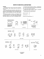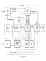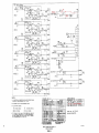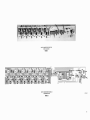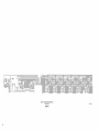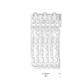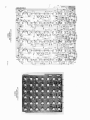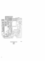
1
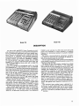
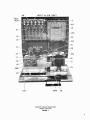
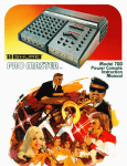
Price $10.00
700 AND 706 SERIES
SERVICE MANUAL
Manufactured by
SHURE BROTHERS INC.
222 Hartrey Avenue
Evanston, Illinois 60204 U.S.A.
Copyright 1981, Shure Brothers Inc.
AL663 (Al) 27A8027
Printed in U.S.A.
SPECIFICATIONS*
Type
. . . . . . . . . . . . . . . . .Solid-state
power console using
discrete components and integrated circuits
Inputs . . . . . . . . . . . . . . . .Six input channels (high andlor
balanced low impedance), plus
two aux input channels (7
and 8)
lnput Channel Controls. VOLUME, INPUT ATTENUATOR,
A/B PAN (700), LOW and HlGH
FREQUENCY EQUALIZATION,
EFFECTSIREVERB, MONITOR
Aux Channel Controls. . .VOLUME, A/B PAN (700)
Master Controls. . . . . . . .MASTER, EFFECTS SEND, REVERB LOW and HlGH EQUALIZATION, REVERB RETURN,
MONITOR MASTER
Outputs . . . . . . . . . . . . . .SPEAKER, MONITOR, EQ OUT,
MIX OUT, EFFECTS, HEADPHONES, AUX, MIC
Common Mix Buses . . . .MIX OUTPUT, EQ OUTPUT (A, B
in 700)
Reverb and Effects . . . . . Built-in reverberation unit; provisions for connection to remote
reverb on-off switch and external effects devices
Graphic Equalizers. . . . .lo-band, fully combining, minimum-phase, octave type, normally connected to power amplifier input; 13 dB boost or cut
at 63, 125, 250, 500 Hz, 1, 2, 4,
8 and 16 kHz; BELOW 63 Hz 12
dB/octave cutoff filter (10 dB
down at 31 Hz)
LED Status Indicators. . . INPUT CLIP, DB PEAKIfeedback
frequency, PA OVERLOAD,
POWER, TEMP WARNING,
SHUTDOWN
706; 700 with
both channels
driven
700 with
one channel
driven
Power Output
Per channel/4 ohms
200W min. 240W typical
125W min. 145W typical
Per channel/8 ohms
Measured at 1 kHz, 120 Vac, 1% THD
Distortion . . . . . . . . . . . .THD typically less than 0.1% at
40 Hz and 1 kHz, 0.25% at 15
kHz; IM distortion typically
less than 0.25% [One channel
driven, 180W or less to 4 ohms,
110W or less to 8 ohms, measured from low-impedance input with individual and master
controls at typical settings
(orange index marks)]
Low- and HighFrequency lnput
Equalization . . . . . . . . ? 13 dB at 100 Hz and 10 kHz
lnput Clipping
Indicators . . . . . . . . . .Light 3 dB below input or equalizer clipping level
DB Peak Indicators.. . . . Indicate power amplifier peak
voltage; +6 dB LED indicates
100 watts sine-wave output to
4-ohm load. Rise time: 250 @ec
to full-scale indication; fall
time: 65 msec from full-scale to
no indication
PA Overload
Indicators . . . . . . . . . .Light when power amplifier THD
exceeds 1% ; fully on at 5%
Temperature Warning
Indicator . . . . . . . . . . .Lights when output transistor
temperature exceeds 70°C
(158°F)
Shutdown Indicator . . . . Lights when power amplifier shutdown occurs due to output
transistor temperature over
100°C (212"F), air flow or fan
failure, or dc at speaker output
lnput Sensitivity
(full power output). . . . BAL LO IMP 0.6 mV
HI IMP
AUX
EQ INPUT
PA INPUT
8 mV
215 mV (700)
106 mV (706)
960 mV
960 mV
SPECIFICATIONS* (continued)
Input Clipping Level.
. . . BAL LO IMP
HI IMP
AUX
Voltage Gain
700 mV to 21 mV
(INPUT ATTEN
-30 to 0)
10V to 335 mV (INPUT
ATTEN -30 to 0)
30V to 10V (VOLUME
from 0 to 10)
. . . . . . . . . .94 dB BAL LO IMP INPUT to
SPEAKER OUTPUTS
71 dB HI IMP INPUT to SPEAKER
OUTPUTS
43 dB AUX INPUT to SPEAKER
OUTPUTS (700; 706: 49 dB)
64 dB BAL LO IMP INPUT to MIX
OUTPUT
77 dB BAL LO IMP INPUT to
MONITOR OUTPUT
74 dB BAL LO IMP INPUT to
EFFECTS OUTPUT
16 dB BAL LO IMP INPUT to MIC
OUTPUT
58 dB BAL LO IMP INPUT to AUX
OUTPUT
81 dB BAL LO IMP INPUT to
HEADPHONE OUTPUT
0 dB EQ INPUT to EQ OUTPUT
30 dB PA INPUT to SPEAKER
OUTPUTS
Levels and Impedances
Nominal Maximum Actual
Working
Circuit
Level
Level
Impedance Impedance
BAL LO IMP INPUT
HI IMP INPUT
AUX INPUT
MIX OUTPUT
EFFECTS OUTPUT
MONITOROUTPUT
EQ INPUT
EQ OUTPUT
AUX OUTPUT
MIC OUTPUT
PA INPUT
SPEAKER OUTPUT
HEADPHONES
5 mV
50 mV
0.5V
1V
1V
1V
1V
1V
1V
5 mV
1V
-
700 mV
10V
30V
9V
9V
9V
1OV
9V
9V
75 mV
1OV
28.3V
1OV
lk
145k
50k
2.4k
2.4k
2.4k
50k
2.4k
5k
70 ohms
50k
360 ohms
19-300 ohms
lOOk or less
10k or less
2k or more
2k or more
2k or more
10k or less
2k or more
2k or more
19-300 ohms
10k or less
4 ohms or more
4 ohms or more
Frequency Response . . . 2 2 dB, 40 to 20,000 Hz, BAL LO
IMP INPUT to SPEAKER OUTPUTS
Hum and Noise
(20 Hz to 20 kHz). . . . . -127 dBV equivalent input (BAL
LO IMP)
Noise
(300 Hz to 20 kHz). . . . -128 dBV equivalent input (BAL
LO IMP)
Signal-to-Noise Ratio . . .Greater than 80 dB (below full
output) at typical control settings (orange marks, MASTER
at 5, INPUT ATTEN at -12)
Mic lnput Simplex
Power . . . . . . . . . . . . .24 Vdc open-circuit, 1.8k series
resistance, simplex o n l o f f
switch
Power Requirements . . .Models 700 and 706: 120 Vac
fl o % , 50160 Hz; 1100W (700),
600W (706) max. (Can be rewired for other voltages; see
OPERATION AT OTHER VOLTA G E S ) ; Models 700E6 and
706E6: 100, 120, 140, 200, 220
and 240 volts, 50160 Hz (switchselectable).
Environmental
Conditions
Operating . . . . . . . . . .-7" to 43°C (20" to 110°F)
Storage . . . . . . . . . . ..-40" to 74°C (-40" to 165°F)
Overall Dimensions. . . . .l9O mm H x 584 mm W x 508 mm
D (7% in. x 23 in. x 20 in.)
Weight
. . . . . . . . . . . . . . .700: 21.3 kg (47 Ib)
706: 17.9 kg (39% Ib)
Construction . . . . . . . . . .Molded construction with black
finish, carrying handle, molded
rubber feet, line cord storage
Certifications . . . . . . . . .Listed by Underwriters' Laboratories, Inc.; listed by Canadian
Standards Association as Certified (700, 706)
*Measurement Conditions (unless otherwise specified): All volume and gain
controls for measured channel at maximum; unused channel controls at 0 ;
equalization controls at 0. Measured input terminated as follows (unused
inputs unterminated): BAL LO IMP, 150 ohms; HI IMP, 33k; AUX. EQ and PA.
4.7k. All outputs terminated as follows: all high-level outputs. 47k; MIC,
150 ohms; SPEAKER, 4 ohms: HEADPHONES, 200 ohms.
TABLE OF CONTENTS
Section
Page
. . . . . . . . . . . . . . . . . . . . . . . . . . . . . . . ii
DESCRIPTION . . . . . . . . . . . . . . . . . . . . . . . . . . . . . . . . . . vii
MAINTENANCE . . . . . . . . . . . . . . . . . . . . . . . . . . . . . . . . . 1
TROUBLESHOOTING . . . . . . . . . . . . . . . . . . . . . . . . . . . . 1
SPECIFICATIONS
CIRCUIT OPERATION
. . . . . . . . . . . . . . . . . . . . . . . . . . . .2
PA Overload LED Indicators . . . . . . . . . . . . . . . . . . . . . 2
DB PeakIFeedback FinderTM LEDS . . . . . . . . . . . . . . . 3
Feedback Finder . . . . . . . . . . . . . . . . . . . . . . . . . . . . . . 3
Power Amplifier Protection Circuits . . . . . . . . . . . . . . . 3
........................ 4
Replacement Parts . . . . . . . . . . . . . . . . . . . . . . . . . . . . . 4
FuseReplacement . . . . . . . . . . . . . . . . . . . . . . . . . . . . . 4
External Parts . . . . . . . . . . . . . . . . . . . . . . . . . . . . . . . . .4
Service Access . . . . . . . . . . . . . . . . . . . . . . . . . . . . . . . 4
Reverb Pan Assembly . . . . . . . . . . . . . . . . . . . . . . . . . . 6
Printed Circuit Boards . . . . . . . . . . . . . . . . . . . . . . . . . . 6
DC Output Balance Adjustment . . . . . . . . . . . . . . . . . 7
DC Bias Current Adjustment . . . . . . . . . . . . . . . . . . . . 7
SERVICE INSTRUCTIONS
DB Peak IndicatorsIFeedback Finder Frequency
Calibration . . . . . . . . . . . . . . . . . . . . . . . . . . . . . . . . . 7
Full Wave Balance . . . . . . . . . . . . . . . . . . . . . . . . . 7
DB Peak LED Calibration . . . . . . . . . . . . . . . . . . . 8
Feedback Finder Calibration . . . . . . . . . . . . . . . . 8
Small Signal and Driver Transistors and
Integrated Circuits . . . . . . . . . . . . . . . . . . . . . . . . . . . 8
Driver Transistors . . . . . . . . . . . . . . . . . . . . . . . . . . . . . 8
Output Transistors . . . . . . . . . . . . . . . . . . . . . . . . . . . . . 8
Diode Bridge Rectifier . . . . . . . . . . . . . . . . . . . . . . . . . . 8
Transistor and Diode Removal . . . . . . . . . . . . . . . . . . . 8
Active Component Checking . . . . . . . . . . . . . . . . . . . . 8
Printed Circuit Board Connectors . . . . . . . . . . . . . . . . 9
Ferrite Bead Rings . . . . . . . . . . . . . . . . . . . . . . . . . . . . . 9
....................... 9
OPTIONAL ACCESSORIES . . . . . . . . . . . . . . . . . . . . . . . 9
GUARANTEE . . . . . . . . . . . . . . . . . . . . . . . . . . . . . . . . . . .9
SHIPPING INSTRUCTIONS . . . . . . . . . . . . . . . . . . . . . . . 9
OPERATION AT OTHER VOLTAGES . . . . . . . . . . . . . . .10
REPLACEMENT PARTS LIST . . . . . . . . . . . . . . . . . . . . .11
NOTES TO SERVICE ILLUSTRATIONS . . . . . . . . . . . .17
SERVICE ILLUSTRATIONS
Model 706
Model 700
DESCRIPTION
The Shure PRO MASTERTM Power Consoles are portable, high-power, eight-input mixer-amplifiers designed for
use by professional entertainers and sound system operators. They are all solid-state units, employing the latest
developments in integrated circuit, discrete component,
and printed wiring technology. The PRO MASTER features
pre-fader monitor, and exclusive FEEDBACK FINDERTM
and PATCH BLOCKTMrear panel. Models 700 and 700E6
are stereo units, with twin 200-watt (rms) power amps, and
Models 706 and 706E6 are mono units, with a single 200watt (rms) power amp.
Six input channels for microphones andlor aux level
sources provide six high-impedance and six balanced
low-impedance inputs (which can be used simultaneously).
Each input channel is equipped with volume, 0-30 dB attenuator, high- and low-frequency equalization, effectdreverb
and monitor controls. Two additional aux (only) input channels (7 and 8) with volume controls are also provided.
Models 700 and 700E6 also contain A I B PAN controls.
LED indicators show input clipping, power amp peak
output level, power amp overload, power-on, temperature
warning, and shutdown conditions.
Master controls include: master volume, effects send,
reverb high- and low-frequency equalization, reverb return
and monitor. Console outputs are: monitor, effects, stereo
headphones, aux, mic, and speakers. In addition, common
mix buses are provided: mix output and equalizer output.
Each 10-band graphic equalizer uses minimum-phase,
combining-type octave filters. Each filter is continuously
adjustable over a 213 dB range, except for the lowest,
which is a 12 dB1octave cut-only switch. The FEEDBACK
FINDER circuit switches the LEDs from power amp peak
output level indicators to visual indicators of feedback
frequency for eliminating feedback by graphic equalizer
adjustment.
The built-in electromechanical spring-type reverberation device has provisions for connecting an external reverb onloff switch through the rear panel.
The rear-panel PATCH BLOCK contains a block diagram
of the console's circuits, with patching jacks located in the
diagram for easy reference.
The Model 700 and 706 consoles' regulated low-voltage
10% range (operpower supplies operate over a 120 Vac
ation as low as 100 Vac is possible at reduced output). The
consoles can be rewired internally for operation at other
voltages (see OPERATION AT OTHER VOLTAGES). An
unswitched ac receptacle for powering accessory equipment up to 100 watts is supplied. The Models 700E6 and
706E6 operate at switch-selected voltages of 100, 120, 140,
200, 220 and 240 volts. Irf all models, a regulated 24 Vdc
simplex supply is provided for powering condenser microphones. The consoles are protected against damage from
open- or short-circuits on inputs or outputs, against heat
damage by a cooling fan and automatic thermal shutdown
circuit, and against radio frequency interference and line
noise.
The structural foam molded cover is fastened to a
19 mm (% in.) wood bottom panel and contains a retractile handle, rubber molded feet, and line cord storage.
Models 700 and 706 are Listed by Underwriters' Laboratories, Inc., and listed by Canadian Standards Association
as Certified.
*
MAINTENANCE
The PRO MASTERTM is an exceptionally well-designed
unit. All components are of the highest quality, operating
well within their respective ratings to assure long life. The
following list of Do's and Don'ts describes minimal operating precautions and maintenance to provide years of dependable service.
DO clean the air filter every 100 hours of operation (more
frequently in dusty or dirty areas). Stand the console on
its rear bumpers, remove the screw securing the filter,
and slide it out of its slot. Rinse the filter i n water or a
mild detergent solution, allow to dry, and replace.
DO unplug the console before cleaning. DO clean the
outer surfaces of the console with a clean, damp cloth
and mild detergent. DON'T use strong solvents or cleaning fluids.
DO use a l6AWG or larger (700, 700E6; 18 AWG for 706
or 706E6) heavy-duty extension cord when additional
line cord length is needed.
DON'T operate the console with air louvers blocked, or
placed on a radiator or heat-producing equipment. Avoid
operation in direct, hot sunlight.
DON'T replace the rear-panel fuse with a different size
or type. Use only IOA, 250V (for Model 700, or 700E6
when operated at 100, 120 or 140 volts), or 5A, 250V,
slow blow (for Model 700E6 when operated at 200, 220
or 240 volts. For Model 706, use a 4A, 250V SLOW BLOW
fuse. For Model 706E6, use a 5A, 250V fuse when operated at 100, 120 or 140 volts, or a 3.15A, 250V SLOW
BLOW fuse when operated at 200, 220 or 240 volts.
DON'T connect the A and B speaker outputs together
(700 or 700E6). (See Instruction Manual for monophonic
setups.)
Console appears to
1. Check air louvers for blockage
be overheating (TEMP
of proper air flow.
WARNING LED on)
2. Check for proper speaker load
or shorted speaker cable.
3. Check air filter and clean if
necessary.
Console power
1. Check for proper air flow (fan
amplifiers turn off
remains on during shutdown).
and remain off
2. Check f o r h o t a i r f r o m l e f t
LED On)
louvers; console may have
overheated (see above). Wait
one minute to allow proper
cooling.
3. Turn console off for a few seconds and turn back on.
4. If shutdown persists, have console checked by qualified service personnel.
No signal at speaker
(all console functions
appear normal)
1. Check for defective or improperly connected speaker cables.
2. Check for improper connections to EQ or PA INPUT.
3. Check settings of channel
VOLUME and MASTER volume
controls.
Console fuse blown
1. Replace with identical fuse.
2. If second fuse blows, have console checked by qualified service personnel.
DON'T risk fire or shock hazard by operating the console
in rain.
DON'T use UNbalanced low-impedance microphones
with the SIMPLEX 24V switch on; turn off the switch
if not required for powering condenser microphones.
If simplex power is in use, connect unbalanced lowimpedance microphones through a line matching transformer (Shure A95FP) to a HI IMP INPUT.
TROUBLESHOOTING
Should any difficulty be encountered in console operation, the problem can often be traced to some simple
source such as an error in interconnection. The following
is offered as a basic guide to this type of problem.
SYMPTOM
Console is "dead"
(no output,
POWER LED off)
1
PROBABLE CAUSE
OR CORRECTION
1. Check that ac power source
is "live" and that console is
plugged in.
2. Check that power ONIOFF
switch is on.
3. Check that rear-panel fuse
is good.
One of two inputs
1. M a k e sure s i m i l a r m i c r o on same channel not
phones are used o n b o t h
working properly (both
inputs, and microphone im%-inch and 3-pin
pedances match the inputs
jacks in use)
used.
2. Make sure microphone is not
used with accessory equipment on other input.
3. Make sure both microphone
switches are on.
INPUT CLIP LED
flashing
1. Adjust INPUT ATTEN to reduce channel input level.
2. Reduce input signal level at
source.
PA OVERLOAD LED
1. Check for defective (shorted)
flashes while DB PEAK
speaker cable.
read less 2. Check that load impedance is
than + 6
not too low (too many speakers
connected).
No DB PEAK/frequen- 1. M a k e c e r t a i n FEEDBACK
cy band LEDindicators
FINDER switch is set to A, B,
flashing (console
ON or OFF (not between positions).
output normal)
No console output;
no DB PEAK LED
indicatorsflashing
1. Check PATCH BLOCKTM rear
panel for improper patching.
2. Check for improper connections to EQ or PA INPUT.
3. Check settings of channel
VOLUME and MASTER volume
controls.
Loud noise or
clicks when certain
microphones or
cables are used
1. SIMPLEX 24V switch is on
(when not needed).
2. Unbalanced cable used when
SIMPLEX 24V switch is on.
3. Check for defective microphone cables.
No monitor output
(program output
normal)
Sound quality poor
(weak or thin)
1. Check MONITOR OUTPUT
connection to EQ or PA INPUT,
or external amplifier.
2. M a k e sure MONITOR and
MONITOR MASTER controls
are turned up.
3. Monitor speaker volume control (if present) may be turned
down.
1. Excessive equalization o n
graphic equalizers.
2. Defective input or patching
cables.
Two simple methods of localizing problems without
opening the console are as follows. These methods can
be used to find the abnormal console section with or without test equipment. (The methods are not needed if the
problem is obvious: SHUTDOWN, no POWER indication,
etc.)
With test equipment: Set all console controls to full
clockwise, REVERB RETURN control to full counterclockwise, and PAN (700) and EQ controls to center. Do not
connect a speaker or headphone load. Apply a 0.5 mV,
1 kHz test signal across pins 2 and 3 of one of the BAL LO
IMP input connectors. Normal voltmeter readings taken
at each speaker, rear-panel PATCH BLOCKTMand frontpanel HEADPHONES connector are given in Table 1.
The top row of figures indicates the voltage i n each stage
from input to output. Similarly, a 5 mV signal inserted in a
HI IMP input will check these same voltages. The other
listed inputs give voltage indications only for those circuits
following the inserted signal. Ac voltages may vary t 3 0 %
from the values shown.
Without test equipment: Using only a microphone and
speaker, it is often possible to isolate problem areas using
the PATCH BLOCK rear panel. The ability to bypass certain circuits and interchange channel signals provides a
simple but powerful tool for troubleshooting. For example,
in a 700 console a suspected channel A equalizer can be
checked by patching between the A MIX OUTPUT and
A PA INPUT jacks. The signal bypasses the equalizer, and
a talk test will immediately indicate whether the problem
has been eliminated.
Similarly, a potentially defective channel B mix amplifier can be verified by patching the A MIX OUTPUT to the
B MIX OUTPUT. The presence of a "clean" signal from
channel A to the B speaker output indicates that the problem precedes the B MIX OUTPUT jack. Further patching
between the EFFECTS OUTPUT and B MIX OUTPUT jacks
will isolate the problem to the B MIX amplifier.
TABLE 1. NOMINAL TEST VOLTAGES
7-
I
I
INPUT
Bal Lo Imp
Hi Imp
Aux (700)
AUX (706)
Eq
PA
I
Monitor Effects
0.5 mV 3.8V
3.8V
5 mV
0.15V
64 mV 0.54V
0.54V
2.7V
2.7V
-
-
I
OUTPUTS
Mix
Aux
Mic
Eq
0.54V
0.54V
0.54V
0.54V
0.54V
0.54V
0.54V
0.54V
7.0mV
7.0mV
7.0mV
7.0mV
0.54V
0.54V
0.54V
0 54V
0.54V
-
-
-
-
-
HeadSpeaker phones*
18.OV
18.OV
18.OV
18.OV
18.0V
180V
11.5V
11.5V
11.5V
11.5V
11.5V
11.5V
'Tip or ring to sleeve.
The above methods are extremely useful for saving time
in localizing problem areas. In addition, they may allow use
of the console in an emergency until repairs can be made.
Internal servicing should only be performed by qualified
service personnel.
CIRCUIT OPERATION
Most of the PRO MASTERTM circuitry uses conventional
operational amplifier technology, and can be serviced
using standard voltage-measurement procedures. However, certain circuits are unusual and may not be familiar
to many servicemen. This section describes these circuits
as an aid to servicing (see Figures 5-38).
PA OVERLOAD LED INDICATORS
The PA OVERLOAD LEOS (01109) are designed to
respond to error signals in their respective differential
amplifiers. The overload circuit is comprised of transistor
Q607 and associated resistors with the LED connected
across the collector and emitter of Q607.
The power amplifier assembly input is the differential
amplifier Q605-Q606, which amplifies the difference of the
signals at the bases (the input signal to Q605 and the negative feedback signal to Q606). With small error signals
(normal power amplifier operation), the dc voltage drop
across R611 is approximately 1.6V, sufficient to keep Q607
turned on. Q607's collector-emitter voltage drop is very
low (approximately O.IV), and as long as Q607 is on, the
associated overload LED is turned off.
When the differential amplifier input signals differ
greatly (such as when clipping or V-l protection takes
place), the ac signal across R611 increases rapidly. At
about 1% distortion, the large ac signal through R611
causes Q607 to turn off. With Q607 turned off, the current
flow is through the associated LED and R616 to ground,
lighting the LED.
Note that the circuit is sensitive to the actual power
supply voltages; if the ac line input voltage is less than
120V, clipping and overload indication will take place at
a lower output level. Note too that the LEDs remain on
during shutdown; this is a normal condition because the
power amplifiers are still partially powered during shutdown.
DB PEAK/FEEDBACK FINDERTM LEDS
With the FEEDBACK FINDER switch (S903) in the OFF
position, LED string D1101-Dl108 indicates peak power
amplifier output voltage values corresponding to indications of -36 to +6 dB at the SPEAKER OUTPUTS. A +6 dB
indication is calibrated through R919 (or R916, Model 700)
for a 20 Vrms sinusoidal output (100 watts to a 4-ohm load).
The power amp assembly (A6) has a resistive voltage
divider at the power amp output that feeds the DB CAL
potentiometer R919. The DB CAL potentiometer sets the
point at which the $6 dB LED turns on. The ac signal is
then forwarded to a full-wave rectifier (U920).
The rectifier is composed of two sections: a unity gain,
inverting precision half-wave rectifier formed by U920A*
and its associated components, and an inverting summing
amplifier formed by U920B, which has two inputs. The first
is via R1045 and R1040, and exhibits a voltage gain of
approximately 1.5 times. The second input is from the output of the precision half-wave rectifier via R1041. The gain
of this input is approximately 3 times.
When the input signal from the power amp is negative,
the output of the precision half-wave rectifier is zero; when
the input signal is positive, the rectifier output is negative.
When the summing amplifier adds the rectifier output and
the non-rectified signal together, the result is an output
voltage that is always positive 1.5 VIN.
The FULL WAVE BAL adjustment (R1045) is used to trim
the gain in one of the summing amplifier paths so that it
is exactly one-half the gain of the half-wave rectifier path.
The output of the full-wave rectifier is fed to the network
comprised of D940, C925 and R1037, which produces the
desired fast attack, slower decay operation. The dc voltage
developed at C925 is fed to the LED comparator string via
the FEEDBACK FINDER switch (S903).
The dc output voltages from U920 drive the comparators
U1101-U1102, which are referenced to a resistive voltage
divider. Each doubling of voltage on the input to the comparators turns on the next higher comparator, causing it
to light its associated LED, as well as keeping the LEDs
below it lit. For example, an input voltage of 1.OV to the
comparator lights the -18 dB LED, as well as the -24,
-30 and -36 LEDS.
Model 700: Note that when S903 is turned to A or B for
feedback determination, the corresponding LED string becomes a readout of frequency for that channel, and the
other channel retains its dB peak indicating function.
FEEDBACK FINDERTM
The Equalizer outputs are fed to the FEEDBACK FINDER
switch (S903) on the Output Controls board (A9), which
selects the desired output channel (A or B in Model 700)
for display. The FEEDBACK FINDER circuit senses the
frequency of the Equalizer signal and converts it to a dc
voltage for display on the selected channel LEDs.
'Channel 8 only: channel A components are shown In the Model 700 A9 Circuit
Diagram.
Amplifier U916B clips the input signal to establish a
square wave of approximately 1.2 Vpp. U916B also contains the FEEDBACK FINDER THRESHOLD control (R999)
which is used to adjust the sensitivity of the circuit. U916B's
output is capacitively coupled to comparator U903A via an
RC filter (R915, C909) that attenuates any ultrasonic noise
present in the signal. The first comparator (U903A) is a
zero-crossing detector, with the operating threshold set
by the amount of hysteresis in the first stage.
The second comparator (U903B) holds capacitor C910
discharged until the output of U903A goes high. The output of the third comparator (U903C) goes high at the same
time as U903A, and stays high until C910 charges to the
reference voltage of 7.5V. This time constant is adjustable
(through R972, FBF CAL) about the nominal 20 ,&ec period
to calibrate the frequency-to-voltage converter. The resultant 20 @ec pulse from U903D is inverted by U903C and
switches a constant current source (Q901) on and off.
Thus, the output of U903D is a pulse train with a constant
pulse width of 20 ~ s e cand a repetition rate equal to the
input frequency. The current pulses are integrated by
capacitor C911 into a dc voltage which is directly proportional to the input frequency (approximately 12 Vdc output
with an input frequency of 11 kHz). The dc output voltage
is fed through switch S903 to the LED comparator strings
to indicate the frequency band. For example, a 1 kHz signal
will produce approximately 1 Vdc at C911 and light the
LED above the 1 kHz graphic equalizer control (and all
lower frequency LEDs: 125, 250 and 500 Hz).
POWER AMPLIFIER PROTECTION CIRCUITS
Each power amplifier is protected by a voltage-current
(V-I) sensing circuit which limits the V-l conditions in the
output transistors to a safe level under overload conditions.
Transistors Q610 and Q611 conduct under overload conditions and remove the input signal from the driver transistors
(Q608 and Q609), thus limiting the dissipation of the output
transistors (Q612-Q615). A single-slope boundary is defined by the values of the resistor network on the bases of
Q610 and Q611.
Thermistors RT602 and RT603 (mounted on transistor
Q614 and Q615 heat sinks) monitor the transistor case temperatures. RT602 and RT603 decrease in resistance as the
case temperatures go up, causing the boundary to "pivot"
to a lower value. The benefit of this arrangement is that
under severe overload conditions, such as operating into
a short circuit, dissipation is limited to a safe value. However, under normal conditions the protection boundary
moves out to allow operation with more severe "normal"
loads than would otherwise be possible. Capacitors C609
and C610 insure stability during limiting.
Q603 provides pre-driver (Q601) protection as follows.
When the current through Q601 reaches a sufficiently high
level during overload, the increased voltage drop through
resistor R614 is sensed by Q603, which then shorts out the
signal to (2601, limiting its collector current to a safe value.
Diodes D609 and D608 are normally reverse-biased and
do not conduct. But with highly reactive amplifier loads, the
diodes will conduct to prevent reverse-voltage breakdown
of the output transistors.
Thermistor RT601 is mounted on output transistor Q613.
Comparators U503A and U503B compare a constant refer-
ence voltage of 0.73V to the voltage across RT601. When
an unusually high temperature of 70°C (158OF) is reached
on the heat sink, RT6Ol's voltage will have dropped to the
reference voltage and U503A or U503B will change state,
turning on theTEMP WARNING LED (D801). If the temperature continues to rise to 100°C (212OF), RT6Ol's voltage
drops below 0.3V, U503C or U503D changes state, turning
off Q502 and Q501, opening relay K1, and turning on the
SHUTDOWN LED (D802). In this condition, the power amps
are partially powered but all other (low-level) circuits and
the fan (BI) remain fully on. This condition remains until
the temperature on the heat sink drops to 70°C, when the
LEDs turn off and full power is restored to the power amps.
RT501 is a positive-temperature-coeffic~entthermistor
with a threshold at 120°C (248OF). It is mounted on the
Power Supply board (A5) in front of fan 61 i n the path of the
air flow through the PC board-fan assembly. When air
motion is severely restricted, RT501 heats and its resistance Increases (from 450 to approximately 1200 ohms).
The current through R502 is reduced and the voltage
drop across R502 is not enough to keep transistor Q501
turned on. (2501 turns off, opening relay K1 and turning
on the SHUTDOWN LED. It is extremely important that
RT501 should be mounted in the path of the air flow, its
body perpendicular to the flow, approximately % " from
and not bent flat against the power supply board.,
The SPEAKER OUTPUTS dc sensor circuit is comprised
of comparator U504 and associated components. A portion
of the output voltage is derived from the divider network of
R640 and R641 on the power amp board. It is fed to the
comparator inputs, and capacitors C509 and C510 remove
the audio signal leaving only the dc component. When the
dc output at the SPEAKER OUTPUTS jacks exceeds 3QV,
U504 changes state, cutting off transistors Q501 and (2502,
opening relay K1, and turning on SHUTDOWN LED D802.
Note that, when the comparator outputs change state,
diode D509 and resistor R518 cause "latching"; the power
switch must be turned off and back on to reactivate the
console. This feature is designed to call attention to the
presence of excessive dc at the output, which is an abnormal condition and probably requires servicing.
placement Kit Number (RKC) or part number, description,
product model number, and serial number.
FUSE REPLACEMENT
To replace line fuse F1, disconnect the line cord from
the ac source and remove the rear-panel fuseholder cap.
Replace the defective fuse as shown in the table. The following rear-panel symbols denote a fast-operating fuse
m
~
and
;
a slow-blow (time lag) fuse
r
T
Model
Voltages in this equipment are hazardous to life.
Refer servicing to qualified service personnel.
REPLACEMENT PARTS
Parts that are readily available through local electronic
parts distributors are not shown on the accompanying Parts
List. Their values are shown on the Circuit Diagrams. Commercial parts not readily available and unique parts are
shown on the Parts List and may be ordered directly from
the factory.
The commercial alternates shown on the Parts List are
not necessarily equivalents, but may be used in the event
that direct factory replacements are not immediately available. To maintain the highest possible performance and
reliability Shure factory replacement parts should be used.
When ordering replacement parts, specify the Shure Re-
Fuse
700
120Vac~10%
700
200,220,240 Vac*
700E6 100,120,140 Vac
IOA, 250V
5A, 250V
IOA, 250V
700E6 200,220,240 Vac
5A, 250V,
Time Lag
4A, 250V,
SLO BLO
3A, 250V,
SLO BLO
5A, 250V
"10%
706
120 Vac
706
200,220,240 Vac*
706E6 100,120,140 Vac
706E6 200,220,240 Vac
3.1 5A, 250V,
Time Lag
Type
3AB, ABC
3AB, ABC
10A/250V
(6.3 x 32 mm)
T5/250V
(5 x 20 mm)
AGC, 3AG
AGC, 3AG
5A/250V
(6.3 x 32 mm)
T3.15/250V
(5 x 20 mm)
'Rewired (see Operation at Other Voltages).
,-CAUTION
+
SERVICE INSTRUCTIONS
Operation at
I
If trouble symptoms-overheating, erratic operation,
etc.-were apparent before the fuse blew, or if the
replacement fuse blows, a qualified serviceman
should troubleshoot the console carefully to find the
source of the trouble. Do not continue to replace
fuses until the trouble is corrected.
I
I
The Consoles also contain four fuses (F501-F504) on
the Power Supply board (A5). If replacement becomes
necessary, replace only with identical fuses. Models 700
and 706 use type 3AG, I A , 250V, SLO BLO, with "pigtail"
leads. Models 700E6 and 706E6 use 5 mm x 20 mm, l A ,
250V, Time Lag fuses.
EXTERNAL PARTS
The following parts can be removed and replaced without disassembling the console:
Air Filter (MP1)
Knob, Rotary (MP2)
Knob, Slider (MP3)
Handle (MP4)
Foot (MP5)
All knobs are pull-off types and are interchangeable.
SERVICE ACCESS
Disconnect the console from its ac power source. To
open the console for servicing, carefully place the console
on a firm, flat surface with the handle upward (sitting on the
rear bumpers). Remove the air filter and remove nine
screws and eight washers securing the bottom panel to the
cover (four from the front and five from the rear of the
bottom panel). Carefully rotate the console until the bottom
panel rests on the work surface and extend either side
A8 \
/INPUT ALIGN. BRKT.
AIO
MP4
PRINTED CIRCUIT BOARD AND
PARTS LOCATION
FIGURE 1
C6
about 5" over the edge of the work surface. Remove the
two exposed screws from the bottom panel. Rotate the
console 180° and remove the remaining two exposed
screws. Lift the cover straight up. When clear of the bottom
panel, rotate it until the cover rests on its rear bumpers.
This "open clamshell" position, with the bottom panel
horizontal and the cover vertical, provides access to all
internal parts and assemblies (see Figure 1).
When closing the console, reassemble as follows to
avoid damage. Remove the air filter (if not already removed). Bend and position the left wiring harness to fold
on top of the PC board-fan assembly. Bend and position
the right wiring harness to fold between the fan and power
transformer, clearing the fan blades. Center the cover over
the bottom panel and lower the cover. With one side of the
console extending about five inches over the edge of the
work surface, replace four screws and washers in the exposed bottom panel holes. Rotate the console so that the
other side extends over the edge of the work surface, and
replace four screws and washers. Raise the front of the
console so that it is sitting on the rear bumpers with the
handle upward and replace the remaining screws and
washers. NOTE: The screw next to the left handle mounting
bracket does not use a washer. Replace the air filter.
REVERB PAN
To remove the reverb pan (AlO), disconnect the input
and output leads from the reverb. Remove the screws and
nuts holding the unit to the bottom cover plate. The cover
plate and foam pads will remain in place. Secure the
replacement pan to the cover plate, making sure the side
of the reverb with the phono jacks faces the front of the
console. Reattach the leads previously removed.
If the console is to be operated with the reverb pan removed, make sure the associated leads are not free to
short out any other wiring. Insulate and tie down the two
reverb cables and ground lead.
PRINTED CIRCUIT BOARDS
The console's printed circuit boards are mounted by
various methods. The following paragraphs describe the
best method of removing each board after cable connectors and connecting wires have been removed. IMPORTANT: When disconnecting cable connectors or soldered
wire connections, make sure connectors or wires are identified for proper reconnection. This may be done by affixing a piece of masking tape marked with the reference
designation (connectors) or terminal letter or color (wires).
Similar wire colors are used in different circuits;
make sure proper re-connections can be made.
Push-on connectors must be removed by pulling
straight out from printed circuit board surfaces. Do
not apply side force when removing or reconnecting
terminals, or damage may result.
Refer to Figure 1 for the location of each board. The
function of each board is given in the following table.
Board
No.
A1
A4
A5
A6
A7
A8
A9
All
Function
Input Controls (Ch. 1-6)
Equalizer
Regulated Power Supply
Power Amplifier (2)
Output Connectors
Input Connectors
Output Controls
LED Board
Component
Numbering
100s, 200s, 300s
400s
500s
600s
700s
800s
900s, 1000s
1100s
A magnetic screwdriver is recommended for removing
boards secured with screws. When removing front-panel
jack retaining nuts with a Y2" nutdriver or wrench, be careful not to damage the surface around the jack. Boards or
parts secured with nylon standoffs may be removed by
using a long-nose pliers to squeeze the locking lugs of the
nylon standoffs on the circuit board side, and sliding the
board outward and off the standoffs. The printed circuit
board connectors can be reconnected for testing purposes
after disassembly from the cover or bottom panel.
lnput Controls (Ch. 1-6) and lnput Connectors Boards (A1
and A8): These boards must be removed at the same time.
Remove the knobs from the left (Input Controls) side of the
front panel. Remove the nine retaining nuts and washers
from the front-panel phone jacks (note that the HEADPHONES jack-J815-has
an insulating washer behind
the metal washer.) Remove connectors J1 and J21 from
the lnput Connectors board and connector J2 from the
lnput Controls board. Remove connectors J24 and J25
from the Output Controls board.
Use a long-nosed pliers to release the locking lugs on the
board standoffs. As each standoff locking lug is released,
push the potentiometer shaft in the vicinity of the standoff
to disengage the board. Repeat this procedure for each of
10 standoffs. As the lnput Controls board is disengaged
from the standoff, all the pot shafts except the six closest
to the lnput Connectors board will fall clear of the top
cover. Using the tips of the long-nosed pliers (or any blunt
object that will clear the pot clearance holes in the cover),
push the six remaining pot shafts through the top cover.
After the lnput Controls board has been disengaged, free
the three phone jacks on the right hand side from the top
cover by grasping the body of the HEADPHONES jack with
the thumb and forefinger, and pulling downward until the
bushing is free from the top cover. Repeat for the AUX
INPUT 7 and AUX INPUT 8 jacks. Free the left side of the
lnput Connectors board by inserting a medium-size screwdriver between the input alignment bracket and the cover.
Start at Channel 6 and lift the screwdriver handle, freeing
the &pin connector and phone jack from the top cover.
Repeat for all six channels. When all six channels have
been freed, the lnput Connectors board and the lnput
Controls board may be lifted out for service.
To reassemble, first make sure that the LEDs are properly positioned. Position the lnput Connectors board in the
top cover (do not assemble nuts or washers at this time).
Position the lnput Controls board at the approximate location of the standoffs. The six rotary pot shafts closest to the
front should be visible through their respective clearance
holes when viewed from the top of the cover. Reach
through the respective clearance holes from the outside
of the top cover using a hooked tool (or a formed paper
clipj and pop the rotary pot shafts into position. The remaining shafts will fall into position. Before snapping the
board into its locked position on the standoffs, check that
the LEDs are aligned with their respective holes. Seat the
board into its locked position. Assemble the washers and
nuts to the phone jacks on the Input Connectors board.
Make sure that the insulating washer is behind the metal
washer on the HEADPHONES jack. Check that the POWER,
TEMP WARNING, and SHUTDOWN LEDs are in their proper
locations. Replace all knobs.
Equalizer Board (A4): This board is located at the center
of the foil side of the Output Controls board (A9). Removal
requires releasing the nylon standoff locking lugs holding
the board in place and pulling the board straight out. Disconnect the wiring harness connectors from J401 and J402.
Regulated Power Supply Board (AS): Remove this board
by disconnecting connectors J7, J8, and J9, and removing
six screws along the edges of the board.
Power Amplifier Boards (A6): The two Power Amplifier
boards (Model 700) are identical except for mounting
brackets. Remove either board by first loosening the PC
board-fan assembly. This is accomplished by removing
four screws securing the boards to the bottom panel.
Select the power amplifier to be removed (channel B
amplifier is toward the front of the console and channel A
is toward the back).
Remove the electromagnetic shield (steel) and electrostatic shield (foil) by disconnecting the grounding lug and
disengaging the shields from the nylon standoffs. Disconnect connectors J13 and J14 (for channel B; J10 and J11
for channel A). Remove three screws from the edge of the
Power Supply board and, using a small Phillips screwdriver, two screws from the fan.
Output Connectors Board (A7): Remove all PATCH
BLOCKTM jack retaining nuts and washers, remove board
connectors J5 and J6 and unsolder three leads (yellow,
green and black) to the MIC OUTPUT jack (PI). The board
lifts straight out of the rear of the cover.
Output Controls Board (A9): Remove the knobs from the
right side of the front panel. Remove the four screws with
lockwashers and insulating washers, and disengage the
five nylon standoffs securing the board to the front panel.
Remove connectors J3, J4, J22, J23, J24 and J25.
LED Board ( A l l ) : This board (two boards in the Model 700)
can be removed after the Output Controls board (A9) is
removed. The LED board is located directly below the
equalizer sliders, and can be removed by lifting upward.
DC OUTPUT BALANCE ADJUSTMENT
In order to eliminate dc offset at the output, a dc balance
control (R601, blue) has been provided for each Power
Amplifier (A6). This control is accessible from the lefthand side of the console. The dc balance should be
checked and adjusted as necessary whenever any Power
Amplifier circuit components are replaced. The dc output
balance adjustment should be made before making the dc
bias current adjustment.
The dc balance adjustment is made with all volume controls down and no speaker load. Connect a dc voltmeter
(preferably with a 0.1 Vdc full-scale range) across a
SPEAKER OUTPUTS jack (J16-J17 for channel A, J18-J19
for channel B).
Use a small screwdriver with an insulated shaft to
make this adjustment; hazardous voltages are present in the circuitry near R601.
Carefully adjust the dc balance control for 0 Vdc -C20 mV
at the output. NOTE: The normal adjustment range of R601
is 1V. If the dc offset exceeds this value, other problems
exist in the circuit.
+
DC BIAS CURRENT ADJUSTMENT
Each Power Amplifier (A6) contains a dc bias current
adjustment control (R617, orange) to set the dc idling
current through output transistors Q612-Q615. This adjustment minimizes crossover distortion without drawing excessive idling power. The bias current should be checked
whenever any Power Amplifier circuit components are replaced. The adjustment should be made after the dc output
balance adjustment. Both dc bias current controls are
accessible from the left-hand side of the console.
The dc bias current adjustment is made with all volume
controls down and no speaker load. Remove the Power
Amplifier board shield and connect a dc voltmeter with a
floating ground across resistor R632 (0.3 ohms, 7W). See
Figures 28-31.
Use a small screwdriver with an insulated shaft to
make this adjustment; hazardous voltages are present in the circuitry near R617.
Starting with the dc bias current control at full counterclockwise, adjust it for 6 f2 mV across R632. The same
voltage should be present across resistors R633, R638 and
R639.
DB PEAK INDICATORSIFEEDBACK FINDERTM
CALIBRATION
The following calibration procedures should be performed when parts in the DB PEAK LED strings have been
replaced. The potentiometers involved on board A9 are the
A DB (R916), B DB (R919), FULL WAVE CAL A (R1044),
FULL WAVE CAL B (R1045), and FBF (R972). The balance
and dB peak calibrations that follow are given for output
channel B; the identical steps for channel A use potentiometers R916 and R1044. All procedures can be performed with the cover open and the Output Controls board
in place (see Figure 1). Note that the first two procedures
apply to the Model 706 and to channel B of the Model 700.
Full Wave Balance
1. Set the console controls to typical settings (orange
index marks), the INPUT ATTENuators to 0, and the
MASTER controls to 5.
2. Feed a 1 kHz, 150 mV signal from a low-distortion
sine-wave signal generator to a channel input HI IMP
jack. With an audio voltmeter connected (without a
speaker load) to a B SPEAKER OUTPUT jack, adjust
the B MASTER or signal generator level control for a
10V output.
3. Connect an oscilloscope across test point TP B (right
center of A9) and ground (see Figures 18 and 20).
The scope display should appear as in Figure 2A or B
if the Full Wave is out of balance, or as in Figure 2C
if it is in balance.
4. If out of balance, adjust the FULL WAVE CAL B
(R1045) until the display looks like Figure 2C (alternate peaks have equal heights).
5. Repeat the above steps for channel A with the scope
on test point TP A.
DB Peak LED Calibration
1. With the console, signal generator and voltmeter set
up as for the Full Wave Balance procedure, vary
the signal generator level so that the output across
the B SPEAKER OUTPUT jack is 20V.
2. Adjust the B DB (R919) until the channel B +6 DB
PEAK LED just barely turns on (dim or flickering).
3. Check for proper operation by decreasing the output
to 19V (the +6 LED should turn off) and increasing
it to 21V (the +6 LED should be on brightly).
4. Repeat the above procedure for channel A.
Feedback FinderTM Calibration
1. With the console, signal generator and voltmeter set
up as for the Full Wave Balance procedure, adjust
the signal generator for an 11.3 kHz signal.
2. Set the FEEDBACK FINDER switch to B or ON.
3. Adjust the FBF (R972) so that the 16 kHz (+6) LED
barely turns on (dim or flickering).
4. Check for proper operation by decreasing the signal
generator frequency to t l . O kHz (the 16 kHz LED
should turn off) and increasing it to 11.5 kHz (the 16
kHz LED should be on brightly).
BALANCE WAVEFORMS
FIGURE 2
SMALL SIGNAL AND PREDRIVER TRANSISTORS
AND INTEGRATED CIRCUITS
All transistors and integrated circuits are mounted on
printed circuit boards. When replacing these parts it is
imperative that proper lead configuration be followed. A
minimum of soldering heat (25W maximum iron) should be
used to avoid damage to the part or printed circuit board.
When replacing regulators U501 or U502, apply Wakefield
Type 120 thermal joint compound to assure good heat
transfer. Refer to the NOTES TO SERVICE ILLUSTRATIONS for transistor and integrated circuit lead codes.
DRIVER TRANSISTORS
Driver transistors Q608 and Q609 are mounted on heat
sink brackets located on the surface of the Power Amplifier boards. Unsolder the transistor leads. When replacing
transistors, apply Wakefield Type 120 thermal joint compound to the surface of the transistor to provide good heat
transfer from transistor to bracket. Be sure that these
transistors are not interchanged in the circuit; they are not
identical devices. Q608 is an NPN transistor and Q609 is a
PNP transistor. Refer to the NOTES TO SERVICE ILLUSTRATIONS for transistor lead codes.
OUTPUT TRANSISTORS
Output transistors Q612 through Q615 are located on the
black, finned heat sinks. The replacement procedure is the
same as that used for driver transistors Q608 and Q609,
except make certain the two diodes mounted below the
heat sinks on Q612 and Q613 are thermally coupled (with
Wakefield Type 120 thermal joint compound) to the heat
sinks above them. Also, make sure that the thermistor
assemblies are replaced, and the output transistors are
replaced in the same orientation as when they were removed. Position the thermistor lead wires so that they are
not in contact with the heat sink or thermistor clip.
NOTE: When replacing output transistors, make certain
the replacement transistor matches the other output transistors in part number and beta code (A, B or C).
DIODE BRIDGE RECTIFIER
Silicon diode bridge rectifier D l is mounted on the bottom panel adjacent to power transformer T I . When replacing this component, apply Wakefield Type 120 thermal joint
compound between the heat sink base of the rectifier and
the bottom panel to provide heat transfer to the bottom
plate. Note that the base of the rectifier is provided with a
locating pin. A notch is provided in the bottom plate to
position the rectifier such that the locating pin fits into the
notch. The terminals are marked to indicate the ac conand "-" dc
nections to the power transformer and the
output connections to filter capacitors C5 and C6.
"+"
TRANSISTOR AND DIODE REMOVAL
Most transistors and all diodes used in the console are
mechanically supported by their leads. When replacing
these devices, proper lead configurations must be followed.
Minimum soldering heat (preferably with a low-wattage25W maximum-soldering
iron) should be used to avoid
damage to the device. Be sure to place heat-shrinkable
tubing or "spaghetti" on leads where the original device
contained such tubing. Transistor lead codes are included
in the NOTES TO SERVICE ILLUSTRATIONS (Figure 4).
ACTIVE COMPONENT CHECKING
Integrated circuits can be checked without removing
them from their circuit board. Measure the input, output
and power supply voltages as shown on the applicable
circuit diagram.
Defective transistors and diodes can be located by use
of a standard ohmmeter such as a Simpson 260. Polarity
of the ohmmeter must be verified before these checks
are made.
With a known diode orientation, measure the diode resistance in the forward and reverse directions. The lowest
meter reading will establish the probe at the cathode end
(schematic symbol arrow points to cathode) as the "minus"
probe while the other probe will be "plus." Some ohmmeters are not polarized i n this manner with relation to
"volts plus probe" and "volts minus probe." With the ohmmeter "plus" probe on the anode end of a diode, and the
"minus" probe on the cathode end, the ohmmeter should
read approximately 2000 ohms or less. With the meter
probes reversed, a reading of about 10,000 ohms or more
should be obtained. If either of these conditions is not met,
the diode should be replaced.
To check LEDs, connect the cathode (notch or flat) of
the LED to the negative terminal of a 9V transistor radio battery. Connect the positive battery terminal through a 4.7k
resistor to the LED anode. Replace any LED that does not
light.
CAUTION
Do not check LEDs with an ohmmeter. The LEDs may
be damaged or erroneous readings may be obtained.
To check transistors, the ohmmeter should be set to the
100- or 1,000-ohm scale. Transistors and diodes must be
removed from the circuit before testing. If all conditions
in the following table are met, the transistor may be considered free of any major defect; if any of the following
conditions are not met, the transistor should be replaced.
See NOTES TO SERVICE ILLUSTRATIONS, Figure 4, for
transistor lead codes.
I
I
OHMMETER CONNECTIONS
"PIYs" Lead
Collector
Emitter
Collector
Emitter
Base
Base
I
64Minus"Lead
Emitter
Collector
Base
Base
Collector
Emitter
I
I
OHMMETER READING
Transistor
NPN
High
High
High
Low
Low
I
Transistor
PNP
I
High
High
Low
Low
High
*
'Not a significant measurement.
PRINTED CIRCUIT BOARD CONNECTORS
All printed circuit board connectors use the Molex KK
Modular Interconnection System. To replace a lead and its
associated connector contact, proceed as follows. Using a
scribe or other pointed instrument, depress the contact
through the slot at the side of the connector housing. This
will free the contact and allow it to be removed from the
rear of the connector housing. Trim a new lead so that
inch of wire appears. lnsert the trimmed lead in a new
contact (Shure Part No. 56A235 or 56A251). Crimp the
wire to the contact and solder the wire to the crimped con-
nection. Insert the new contact (with attached lead) in the
connector housing, pushing firmly to lock the contact.
FERRITE BEAD RINGS
All input and output connectors in the console contain
ferrite bead rings (L701-L711 and L801-L816). Be sure to
replace any ferrite bead rings removed during servicing.
SERVICE ILLUSTRATIONS
Immediately following the parts list on the pages that
follow are circuit diagrams, parts locating photographs,
and board foil drawings. Once a board has been located
through the parts location photo (Figure I ) , the components
on that board can be located from the corresponding parts
location photo. The function of the part is shown on the
adjacent circuit diagram. NOTE: Each circuit diagram
applies to all 700 Series consoles. Portions shown in red
only apply to Models 700 and 700E6. Further differences
are shown in notes at the bottom of each diagram.
OPTIONAL ACCESSORIES
The following optional accessories are specially designed for use with the Shure 700 Series Power Consoles:
A700C Protective Cover
A7S Console Stand
GUARANTEE
This Shure product is guaranteed in normal use to be
free from electrical and mechanical defects for a period of
one year from date of purchase. Please retain proof of
purchase date. This guarantee includes all parts and labor.
This guarantee is in lieu of any and all other guarantees or
warranties, express or implied, and there shall be no recovery for any consequential or incidental damages.
SHIPPING INSTRUCTIONS
Carefully repack the unit and return it prepaid to:
Shure Brothers Incorporated
Attention: Service Department
1501 West Shure Drive
Arlington Heights, Illinois 60004
If outside the United States, return the unit to your dealer
or Authorized Shure Service Center for repair. The unit
will be returned to you prepaid.
OPERATION AT OTHER VOLTAGES
The Model 700 and 706 consoles are supplied wired for
operation at an input of 120 Vac *10°/~, 50/60 Hz. For operation at 240V, 220V, 200V, 140V or 100V, follow the steps
listed below. Open the cover as described in SERVICE
ACCESS. Remove the screws securing the PC board-fan
assembly to the bottom panel and remove the assembly to
provide working room. For 240V, 220V or 200V operation,
unsolder and insulate the black lead from fuseholder XFl
to UNSWITCHED AC receptacle J20 (J20 will be inoperative at these voltages). NOTE: Fan B1 is permanently
wired and will continue to operate at 120 Vac with the
following wiring changes. (Figure 3 illustrates terminal
strip TSl, located between transformer T I and fan B1,
and the jumper and transformer T1 leads which must be
moved.)
240V Operation:
1. Cut the bare jumper between the redlblack and blue1
white leads.
2. Unsolder the yellowlblack lead and solder it to the
redlblack lead.
220V Operation:
1. Perform the above steps for 240V operation.
2. Unsolder the white (AC) lead from the bluelwhite lead
terminal and solder it to the terminal with blue and
yellow leads.
200V Operation:
1. Cut the bare jumper between the redlblack and blue/
white leads.
2. Unsolder the yellowlblack lead and solder it to the
white transformer lead.
3. Unsolder the white (AC) lead and solder it to the
terminal with blue and yellow leads.
140V Operation:
1. Cut the bare jumper between the red/black and blue/
white leads.
2. Unsolder the blue lead and solder it to the redlblack
lead.
3. Unsolder the white transformer lead and solder it to
the yellow lead.
100V Operation:,
1. Unsolder the white (AC) lead and solder it to the white
transformer lead terminal.
2. Solder a jumper wire between the white transformer
lead terminal and the terminal with blue and yellow
leads.
Reposition the power harness and mount the PC boardfan assembly before testing the unit. For 240V, 220V and
200V operation, obtain a suitable ac plug and attach it to
the line cord. Obtain a 5A, 250V, type 3AB or ABC fuse
(for the 700 console), or a 3A, 250V, SLO BLO, type AGC
or 3AG fuse (for the 706 console), and insert it in place of
the present fuse. Check for proper operation by measuring
voltage across capacitor C5 or C6: Under no-signal conditions, the voltage should be 54V t 3 V . Be sure to mark the
rear panel with the new operating voltage.
As supplied, Model 700E6 and 706E6 consoles are set to
operate from 240 volts. To change operating voltages, disconnect the ac power (mains) cable, select the desired
operating voltage using the rear-panel VOLTAGE SELECTOR switch, and make certain the fuse ( F l ) is of
the proper value.
TRANSFORMER REWIRING
FIGURE 3
REPLACEMENT PARTS LIST
This list describes parts for Models 700, 700E6, 706 and 706E6. Major differences between parts are shown by multiple
listings of the part with parenthetical notation of the models. When servicing 706 and 706E6 consoles, disregard reference designations given for parts not present in these models.
Reference
Designation
Replacement
Kit No.*
Replacement Kit Consists Of:
Qty.
Part No.
Description
Commercial
Alternate
A1
-
lnput Controls (Ch. 1-6)
Board (700,700E6)
None
A1
-
lnput Controls (Ch. 1-6)
Board (706, 706E6)
None
A4
-
Equalizer Board
None
A5
-
Power Supply Board (700)
None
A5
-
Power Supply Board (700E6)
None
A5
-
Power Supply Board (706)
None
A5
-
Power Supply Board (706E6)
None
A6A
-
Power Amplifier Board,
Ch. A (all models)
None
A6B
-
Power Amplifier Board,
Ch. B (700,700E6)
None
A7
-
Output Connectors Board
(700, 700E6)
None
A7
-
Output Connectors Board
(706, 706E6)
None
A8
-
lnput Connectors Board
(700, 700E6)
None
A8
-
lnput Connectors Board
(706, 706E6)
None
A9
-
Output Controls Board
(700,700E6)
None
A9
-
Output Controls Board
(706, 706E6)
None
A1 0
-
Reverb Pan
None
A1 1
-
LED Board
None
B1
Fan, Cooling, 70 CFM
Rotron WR2HI
C5, C6
-
Capacitor, Electrolytic,
800OPF, 60 W V ~ (700,700E6)
C
None
C5, C6
-
Capacitor, Electrolytic,
4000 ,uF,60 W V ~ (706,706E6)
C
Sprague
36D252F075AC2A
C101, C103,
C111, C112,
C201, C203,
C211, C212,
C301, C303,
C311, C312,
C508, C513,
C904, C905,
C911, C918,
C930
-
Capacitor, Electrolytic,
.,, 35 Wvdc
4.7 or 5 F
Sprague, 30DTE1303; CDE
NLW-5-50
'Parts listed as RKC K ~ t sshould be ordered by
quantit~es.
at kit nun 3er. Any orders received for piece parts where RKC Kit number i s shown will be shipped i n RKC
REPLACEMENT PARTS LIST
Reference
Designation
Replacement
Kit No.*
C315, C316,
C605, C703,
C718, C928,
C929
-
C447, C448,
C915, C924,
C926, C927
-
Replacement Kit Consists Of:
Qty.
-
Part No.
Description
Commercial
Alternate
86N628
Capacitor, Electrolytic,
100 ,LF, 25 Wvdc
Sprague 30DTE1211; Mallory
MTA-100F35; CDE
NLW-100-25
86F629
Capacitor, Electrolytic,
4.7 p.F, 25 W V ~ C
Sprague
503D475G025
86A632
Capacitor, Electrolytic,
1000 ,LF, 25 W V ~ C
Sprague TVA-1211
868632
Capacitor, Electrolytic,
1000 ,LF, 40 Wvdc
None
C501, C502
-
C503
-
C504
-
-
86C629
Capacitor, Electrolytic,
33 pF, 16 Wvdc
None
C507
-
-
86B636
Capacitor, Electrolytic,
4 pF, 25 Wvdc
Mallory
TNT405U050POA
C819
-
-
86L628
Capacitor, Electrolytic,
220 or 250 pF,40 Wvdc
CDE BR250-50
C901, C902,
C908
-
-
86B629
Capacitor, Electrolytic,
22 pF, 35 Wvdc
Sprague 502D226G050CEl C;
Mallory MTV-25B35
D1
-
-
86A640
Silicon Rectifier, 200V,
25A
Varo VT200/T
RKC21
4
86A404
Silicon Rectifier, IOOV,
1/2A
Motorola 1N4002
-
-
86D422
Diode, Light-Emitting
Monsanto
MV5075C
D l 03-Dl 06,
D203-D206,
D303-D306,
D509, D510,
D604, D605,
D701-D708,
D901-D906,
D925-D936,
D938, D939,
D941, D942
-
-
86A415
Diode, Silicon, Computer, 75V
TI or GE 1N4148
D507
-
-
86A428
Silicon Zener Diode, 24V, 5W
Motorola 1N5359A
D606, D607
RKC50
2
86A410
Silicon Rectifier, IOOV, 1/2A
Motorola 1N4002
D608, D609
RKC46
4
86A406
Diode, Silicon, 200V, 3A
Motorola 1N4721
D937, D940
RKC19
4
86A405
Diode, Germanium, 30V
RCA 1N48,l N60
-
-
80C323
Fuse, IOA, 250V (700)
Littelfuse 314010
D2, D501-D506,
D508, D601D603, D803,
D943, D944
Dl01, D102,
D201, D202,
D301, D302,
D801,D802,
D804, D l 101Dl109
F1
-
'Parts listed as RKC K ~ t sshould b e ordered by that kit number. Any orders r e c e ~ v e dfor piece parts where RKC Kit number i s shown w i l l b e shipped in RKC
quantities.
12
REPLACEMENT PARTS LIST
Reference
Designation
Replacement
Kit No.*
Replacement Kit Consists Of:
Qty.
Part No.
Commercial
Alternate
Description
F1
-
-
80A380
Fuse, Slo-Blo, 5A, 250V (700E6)
Littelfuse 213005
F1
-
80E159
Fuse, Slo-Blo, 4A, 250V (706)
Littelfuse 313004
F1
-
808258
Fuse, Slo-Blo, 3.15A, 250V (706E6)
Littelfuse 21303.15
F501-F504
-
-
80A268
Fuse, Pigtail, Slo-Blo, 1A, 250V
(700,706)
Littelfuse 315001
F501-F504
-
-
808380
Fuse, Time Lag, 1A, 250V
(700E6, 706E6)
Schurter 034.31 17
J1-J8, JIO,
J11, J13, J14,
J21-J25,
J401-J402
-
-
56A251
Connector Contact (only)
None
J9
-
56A235
Connector Contact (only)
None
J16-J19
-
-
90BA2600
Phone Jack, 2-Conductor
Switchcraft 11
J20
-
-
95A8005
Outlet, UNSWITCHED AC (700, 706)
None
J 30
-
-
95A898
Receptacle, AC Power Line (700E6)
Otto Heil 161-6
J30
-
-
95A689
Receptacle, AC Power Line (706E6)
Otto Heil 6061-3
J701-J705,
J707, J709,
J710, J801,
J803, J805,
J807, J809,
J811, J813,
J814
-
-
90BL2600
Phone Jack, 2-Conductor
None
J707, J708,
J711, J712
-
-
90BK2600
Phone Jack, 3-Conductor
None
J802, J804,
J806, J808,
J810, J812
-
-
95A899
Connector, Receptacle,
3-Pin
None
J815
-
-
90BJ2600
Phone Jack, 3-Conductor,
HEADPHONES
None
K1
-
-
55A145
Relay, DPDT
None
-
95A8004
Choke Coil, 4.7 pH
None
L701-L711,
L801-L816
-
-
80A365
Ferrite Bead Ring
Stackpole 57-3425
MPI
-
90BM2600
Air Filter Assembly
None
MP2
-
-
90A8101
Knob, Rotary
None
MP3
-
-
90A2950
Knob, Slider
None
MP4
-
-
65A8013A
Handle
None
MP5
-
-
66A158
Foot
None
MP6
-
-
66A164
Rear Bumper
None
-
90E2232
Connector, Plug, 3-Pin,
MIC OUTPUT
Switchcraft D3M
L601
PI
*Parts listed as RKC Klts should be ordered by that klt number Any orders recelved for piece parts where RKC KII pumber
auantltles
I
shown will be shipped i n
REPLACEMENT PARTS LIST
Reference
Designation
Replacement
Kit No.*
Replacement Kit Consists Of:
Qty.
Part No.
Description
Commercial
Alternate
Q501, Q603,
Q607
RKC66
1
86A335
Transistor, Silicon, PNP
TI TIS93
Q502
RKC65
1
86A334
Transistor, Silicon, NPN
TI TIS92
Q601
-
-
86A8301
Transistor, Silicon, Power, PNP
None
Q602, Q605,
Q606
-
-
86A355
Transistor, Silicon, NPN
Motorola MPS-A06
(2604
-
-
86A8300
Transistor, Silicon, NPN
None
Q608
-
-
86A361
Transistor, Silicon, NPN
RCA 2N6263
(2609
-
-
86A362
Transistor, Silicon, PNP
Motorola 2N3741* *
(2610
-
-
86A363
Transistor, Silicon, Power, NPN
Motorola MPS-A20T
Q611
-
-
86A364
Transistor, Silicon, PNP
Motorola MPS-A70T
Q612-Q615
-
-
86A378
868378
Transistor, Silicon, Power, NPN
Transistor, Silicon, Power, NPN
Motorola 2N3773tT
RCA TA8638ASt
Q901, (2905
-
86A348
Transistor, Silicon, PNP
Motorola 2N5087
Q902
-
-
86A352
Transistor, Silicon, Power, NPN
Motorola MPS-UO2;
GE D40D4
Q903
-
-
86A353
Transistor, Silicon, Power, PNP
Motorola MPS-U52;
GE D41D4
(2904
-
-
86A329
Transistor, Silicon,
N-Channel, Field Effect
Motorola 2N5458
R1, R2
-
-
45EC561B
Resistor, 560, 5\N, 10%
IRC or Dale PW-5
R3
-
45EC252B
Resistor, 2.5k, 5W, 10%
IRC or Dale PW-5
R102, R107,
R115, R116,
R148, R149,
R202, R207,
R215, R216,
R248, R249,
R302, R307,
R315, R316,
R348, R349,
R997
-
-
46B82
Potentiometer, Linear
Taper, lOk
None
R118, R119,
R126, R127,
R218, R219,
R226, R227,
R318, R319,
R326, R327,
R995, R996
-
-
46C82
Potentiometer, Linear
Taper, 50k
None
R131, R132,
R231, R232,
R331, R332,
R926, R939
-
-
46D82
Potentiometer, Linear
Taper, lOk
None
**Parts listed as RKC Kits should be ordered by that kit number. Any orders received for piece parts where RKC Kit number is shown will be shipped in RKC
quantities.
"Selected for 120V BV,.l.:o min.
tUse in emergency only. Select for high gain. May affect power output and reliability.
t t M u s t be matched for manufacturer and beta value.
REPLACEMENT PARTS LIST
Reference
Designation
Replacement Kit Consists Of:
part NO.
1
46A82
Commercial
Alternate
Description
Potentiometer, Audio
Taper, 1OOk
None
Potentiometer, IOk, Dc
Output Balance
None
Resistor, 1.5k, 5W, 10%
IRC or Dale PW-5A
Potentiometer, 100, Dc
Bias Current
None
45HB309C
Resistor, 0.3, 7W, 5%
IRC or Dale PW-7A
45HC561 B
I Resistor, 560,5W, 10%
IRC or Dale PW-5A
45HC220B
Resistor, 22,5W, 10%
IRC or Dale PW-5A
46B84
Potentiometer, Linear
Taper, 10k
None
46E82
Potentiometer, Audio
Taper, 100k
None
46B83
1 Potentiometer. Slide.
None
45A43
I
None
46F33
45HC152B
46G33
90A2790
86A904
1I
1 Thermistor Assembly. NTC
1
55A139
55A141
55C119
1
55A99
55E140
55E135
1
51A282
51A285
9082150
Thermistor, PTC
11
None
Metal Oxide Varistor,
56V
GE V56MA2B
Switch, Rocker, SPST,
ON/OFF (700,706)
Cutler-Hammer
8021-K25M1V
Switch, Rocker, SPST,
ON/OFF (700E6,706E6)
Marquardt 1601
Switch, Slide, DPDT.
SIMPLEX
None
Switch, Rotary, VOLTAGE
SELECTOR (700E6,706E6)
Schurter SWP
033.3007
Switch, Slide, DPDT,
BELOW 63/FLAT
None
Switch, Slide, TPTT,
FEEDBACK FINDERTM
None
Transformer, Power
(700, 700E6)
None
Transformer, Power
(706, 706E6)
None
Output Transformer and
Shield
None
'Parts listed as RKC Kits should be ordered by that k ~ number.
t
Any orders received f o r piece parts where RKC Kit number i s shown w i l l be shipped In RKC
quantities.
15
REPLACEMENT PARTS LIST
Replacement
Kit No.*
Reference
Designation
Replacement Kit Consists Of:
Part No.
Description
Input Transformer and
Shield Assembly
None
lntegrated Circuit, Quad
Operational Amplifier
Raytheon
RC4156DB * *
lntegrated Circuit, Quad
Comparator
Raytheon LM339DB
lntegrated Circuit, Quad
Operational Amplifier
Raytheon RC4156DB
lntegrated Circuit,
Voltage Regulator,
Positive
Motorola
MC7815CT
lntegrated Circuit,
Voltage Regulator,
Negative
Motorola
MC7915CT
lntegrated Circuit, Dual
Operational Amplifier
Raytheon
RC4559NB
Ac Cable and Plug, 91/2 ft,
3-Conductor (700)
None
Ac Cable and Plug, 9 ft,
3-Conductor, Single
Connector (700E6)
None
Ac Cable and Plug, 91/2 ft,
3-Conductor (706)
None
Ac Cable and Plug, 9 ft,
3-Conductor, Single
Connector (706E6)
1
Commercial
Alternate
1
None
Fuseholder (700,706)
Littelfuse 341001
Fuseholder (700E6,706E6)
Schurter FEC
I
'Parts listed as RKC Kits should be ordered by
quantities.
**Selected for low noise figure.
at kit number. Any orders received for piece parts where RKC Kit number is shown will be shipped
In
RKC
NOTES TO SERVICE ILLUSTRATIONS
GENERAL
The pages that follow contain interconnection diagrams,
circuit diagrams, parts locating photos and board foil
drawings.
Shure part numbers are not shown in the Parts List if
parts are readily available through local electronics parts
suppliers. In these instances, the circuit diagrams show
only the reference designation and value of the standard
parts.
All capacitor values are shown in microfarads unless
otherwise designated. All non-electrolytic capacitors are
50 working volts dc or more unless otherwise specified.
Electrolytic capacitors are shown in microfarads x volts.
INTEGRATED CIRCUITS
All resistor values are shown in ohms-(k = 1000). Resistors are 5% tolerance unless otherwise specified. Resistors
are-%-watt unless otherwise specified.
Transistor lead codes are shown in Figure 4. Acceptable
replacements are shown in the Parts List.
The following ground symbols denote:
Chassis Ground
d7
Circuit Ground
&
Printed Circuit Board Ground
1
6
f
ANODE
4
CATHODE
NOTCH
UIOI, U102.U201,U202,
USOl. U302, U401-U404,
w o 3 , ~(104,~ 7 0 1usoa,
,
ume, WIOI, u11o2
U913
- U92I
U501, U 5 0 2
6
"'
DIOI. D102. D201, D202,
DSOI, D302,D801,0802,
0804, Dt161 01409
-
(TOP VIEWS1
(BOTTOM VIEW)
(BOTTOM VIEW)
(BOTTOM VIEWS)
(BOTTOM VIEWS)
(BOTTOM VIEW1
LEAD CODES
FIGURE 4
NOTE: The ÿ ire Interchange" footnotes shown below
the connector tables in the circuit diagrams are for manufacturing purposes only. Wires should not be interchanged
during servicing as incorrect ohmmeter readings may
result.
TROUBLESHOOTING
A general troubleshooting process is as follows: If the
console is completely "dead," check the ac power source,
fuses, chassis power supply output (54V across capacitors
C5 and C6), regulated power supply (+15V between pin E
and ground, connector P502, or -15V between pin M and
ground, P503, board A5). If the POWER LED is on but the
output is low or not present, follow the procedure described under TROUBLESHOOTING in this manual. Following localization of the problem, determine that the
input and output voltage to the board is correct. If an incorrect voltage is found, perform Ac and Dc Voltage Measurements as described below to isolate the problem area.
AC VOLTAGE MEASUREMENTS
The numbers within rectangular symbols
on the
circuit diagrams denote the ac voltages at that point under
the following test conditions:
1. Voltages measured with respect to chassis unless
otherwise indicated.
2. Line voltage: 120V, 60 Hz.
3. Test signal of 0.5 mV, 1 kHz applied across pins 2 and
3 of connector J802.
4. Ac voltage measurements may vary +30% from
values shown.
5. Measurements made with ac VTVM of 1 megohm or
greater input impedance.
6. No load on SPEAKER OUTPUTS jacks (J16-J19).
7. All controls in full clockwise settings.
8. REVERB RETURN set to full counterclockwise.
9. PAN (700) and EQ controls set to center.
DC VOLTAGE MEASUREMENTS
The numbers within elliptical symbols 0 on the circuit diagrams denote the dc voltages at that point under
the following test conditions:
1. Voltages measured with respect to chassis unless
otherwise indicated.
2. Line voltage: 120V, 60 Hz.
3. No input signal applied.
4. Dc voltage measurements may vary +20% from
values shown.
5. Measurements made with VTVM of 11 megohms or
greater input impedance.
RESISTANCE MEASUREMENTS
With the ac line cord disconnected from the ac source
and the Power ONIOFF switch in the OFF position, the
following ohmmeter measurements may be made:
1. Reverb pan A10 output coil: approximately 360 ohms;
input: approximately 40 ohms.
2. Transformers may be checked for continuity of each
winding.
3. To test transistors and diodes, refer to the section on
ACTIVE COMPONENT CHECKING.
INPUTS
1- 8
AC
LINE
INPUT
I
+55V
I
FZA. O V E R L O A D
MODEL 700 AND 706 BLOCK DIAGRAM
FIGURE 5
Pa02
D
STEREO
C
HEADFWNES
J813
T
POWER
I
-L
AUX INPUT 7
JBI 3
1814
AUX IbJPUT 8
,,BLU w24-- A
I
caer
I
T
- IOOPF
'
r
c
DLK *24
CONNECTOR: P802 (J21)
I,
FUNCTION
IN pF AND 50V OR MORE UNLE55 OTHERWISE SHOWN,
ELECTKOLYTlC CAPACITCi?S SMCWM IN ,kF X VOLTS.
A L L CAPACIT-
2. bLL RESI5TORS 1/4W, 5% UNLESS OTHERWISE SHOWN.
3. THE F O L L W N G CENCTE :
1$7
CUA5515 6IIOLND
0D.C. V o l T A C E
MODEL 706: J815 TIP AND
RING ARE CONNECTED.
4. TE5T SIGNAL OF S m V , 1 K H t APPLIED AGO55 PIN5 2 A N D 3 OF
LOW IMPEMNCE CONNfCTORS. AC VOLTAGE MEASLREMENT.
MAY VARY f 30 % GROM V A W E S SHOWN. ALL P.C. 8 0 A R G 5
ARE IUTERCDNNECTED AS IN FINAL UhJIT.
INPUT CONNECTCRS BOARD A8
CIRCUIT DIAGRAM
FIGURE 6
I
INPUT CONNECTORS BOARD A8
PARTS LOCATION
FIGURE 7
INPUT CONNECTORS BOARD A8
COMPONENT SIDE
FIGURE 8
INPUT CONNECTORS BOARD A8
FOIL SIDE
FIGURE 9
INPUT CONNECTORS BOARD A1
FOIL SIDE
FIGURE 10
I
MIS
.
NOTES :
CONNECTOR : PI01 ( J 2 )
\.ON INPUTS 3 AND 4 ( A Z ) ADD 100
ON INPUTS 5 AND 6 (43)ADD 260
EXCEPT C315, C316.
TO
R L L C , D , R AND U N U M B E R S .
TO ALL
C , D,R
ilND
U
\"JMBLRS
2. ALL CAPACITORS IN p F AND W V OR MORE UhiLECC OTHERWI5E
3HOWN. ELECTROLYTIC CAPACITOR5 SHOWN IN ,uF r VOLTS.
MODEL 706: R111, 113 ARE
56K; R105, R108 ARE JUMPERS.
3.ALL RESISTORS 1/4 w ,5% UNLESS OTHERW I5E SPELIFzIED.
4.THE FOLLOWING SYMBOLS DENOTE :
P.C BOWD G R O U N D
0D.C. VOLTAGE
nA . ~ . ~ o L T A G E
4. TEST ZIGNAL CF 6 mV, I U H t APPLIED BETWEEU 3LU AND BLK INPUT
WIRES FROM 33K OHM 5 W R C E . ALL VOLTAGES MEASUREL) AT
2 5 O C WITH 120 VAC AM0 ALL P. C. W A R D S INTERCONNECTED
65 IN PINAL UNIT. VOLTAGE MEASLIHmEN'E M A Y VARY
f 30% FROM VALUE5 SHOW
b. EQ
L
#24
IwW/BLC(
M
$+24
a24
W G -
P
W
- R-
q
WHTt
N
(J7) P503F
(J7) D503M
(J8)
P502G
CLOCKWISE.
+
N.C.
(J7)
P503N
AND PAN W T R O L S 'CENTERED. ALL OTHER COIJTKO-5
FULLY
INFUTCUPPINC LED GROUND
INPUT,CUF(WGLED - 15V
15V
INPUT CONTROLS BOARD A1
CIRCUIT DIAGRAM
FIGURE 13
- 15V
2
LK
I
I
A + I3 AUX. OUTPUT
I
0 MIX OlJTPUT
I
P701
1
A
--------x
6
P702
U7Ol
86A806
C/-
C
D
E
7
E-
BAL LG IMP
F
,-
G
H
J .
K .
\
I
L
R7Z8
J71 I
MONITOR 0UTPL)T
1
C
-v
$1
E
F
G
A PA INPUT
D7&7 C
%A415
-L'
R722
C720
33K
REVERB SWITCH
R
I
-@
0704
66A415
0717
I
~724
I'VI
J7l2
\
J
I
G725
W
B PA INPU
I
I
EQ OUTPUT
-I. A L L C A P A C I T O R S I N
F AND 50V
OTHEHVJISE SHOWN. &ECTRGLYTIC
IN ,uF
X
--
--
--
--
OR MORE UNLE55
CAPACITORS
SHOLJU
VOLTS.
2 . A L L RESISTORS 1 /4 W , 5% UNLESS OTHERW,SE S H O I ~ N .
3.THE FOLLOkriNG SYMBOCS DENOTE :
,j, CHA351S
P.C. BOARD
GROUND
0D. C.
VOLTAGE
b_J A .C. VOLTAGE
4. All- VCXTAtES MEASWED AT 25-C WITH IZOV AC, INPUT AT I KHz
AND &L PC BOARDS INTERCWEfJTED A5 IN FIUNIT.
LOLTAGE VALUE5 ARE WPICAL AND M Y VARY f 30%.
t WIRES CAN BE
*
WIRES CAN BE I N T E R C H A W
IN EARLIER MODE.^ :
INTEWAtJGED.
MODEL 706: D702, R713, R716, R719,
R722 ARE JUMPERS.
OUTPUT CONNECTORS BOARD A7
CIRCUIT DIAGRAM
FIGURE 14
OUTPUT CONNECTORS BOARD A7
PARTS LOCATION
FIGURE 15
OUTPUT CONNECTORS BOARD A7
COMPONENT SIDE
FIGURE 16
OUTPUT CONNECTORS BOARD A7
FOIL SIDE
FIGURE 17
,TEST
POINT
P
FULL
WAVE
BAL
.TEST
POINT
DB
'C A L
OUTPUT CONTROLS BOARD A9
FOIL SIDE
FIGURE 18
OUTPUT CONTROLS BOARD A9
PARTS LOCATION
FIGURE 19
OUTPUT CONTROLS BOARD A9
COMPONENT SIDE
FIGURE 20
1 PIN&
C
24
22
I
1
VlO
GRN
I
(J6) P7SI J IMONITGK
9UTPUT
LM!PLO^LC(B)
I"B"FEAK:NDLCATOR DRIVE
22
?
ORN
(JII)F.LOZC(A)I X.. PEAK 1NDICATOR DRIVE
i
G
H
.-
J
-ES.
I A L L C A P A C I T O R S I N w F A N D 5 0 V O R M O R E UNLESS
OTHERWISE SHOWN. E L E C T R O L Y T I C CAPACITORS SHOWN
I N , u F x VOLTS
2 . A L L RESISTORS 114 WATT, 5 % UNLESS OTHERWISE SPECIFIED.
3.THE FOLLOWING S Y M B O L S DENOTE.
&
R C . B O A R D GROUND
v
(3D.C
4 ALL VOLTAGES MEASURED AT 2SeC W I T H I20VAC,lNPUT
AT IK H \ A N D A L L P C BORRDS I N T E R - CONNECTED
AS I N FINAL UN\T. VOLTAGE VALUES ARE TYPICAL AND
MAY VARY t ZOqo
L
5 REVERB RETURN CONTROL FULLY COUNTERCLOCKWISE.
?AN AND € 9 CONTROLS CENTERED.
ALL OTHER CONTROLS FULLY CLOCKWISE.
!p
li
K
;
-.l*co;mD~
€ ;A; [
IELIBLK
AC VOLTAGE
VARIABLE WITH FREQUENCY:
o-lev
-
N
p
R
- .
--
OUTPUT CONTROLS BOARD A9
CIRCUIT DIAGRAM
.- .
-
KC.
S I G N A L GROUND
SIGNAL GROKN-D-
NC
SIGNAL GROUND
-
FIGURE 21
W3
TO
(re) p w z u
(J6)P 7 0 1 L
FINDER)
24
COLOR
TO
I
BLACK
A8 C820
NO CONNECTION
BLUE
( ~ LR13
8
FUNCTION
AUX "7"GROUND
SIGNAL G R O U N D
A U X "7" INPUT
,
PIN*
FUNCTION
+ISVDC(FEEDBACK
24
D
F
ZONNECTION
( ~ 6P7OI
) F
A
WHT
SHIELD
/ A10
NO CONNECTION
WHT /ELK
VOLTAGE
t 1 5 v W l T H LED OFF
.5V WlTH LED O N
NO
I GAUGE I
GAUGE
COLOR
A
24
BLUE
C
24
BLAPK
TO
A8 L E I 4
FUNCTION
AUX."8' INPUT
EFFECTS OUTPUT
GROUND (PEAK RECTI FICR)
REVERB RETURN (HOT)
EVERR RETURN(~HIELD/~>D\
A 8 "821
A:X
"a"GROUND
I
IOOK
LED BOARD A l l
PARTS LOCATION
FIGURE 22
TOP FOlL
CAPACITORS INpF
OTHERWISE SHOWN.
I. ALL
BOTTOM FOlL
AND
50V
OR
2. ALL
RESISTORS
1/4 W . 5% UNLESS
3. THE
FOLLOWING
SYMBOLS
DENOTE
MORE
UNLESS
OTHERWISE
SHOWN.
:
6
P.C. B O A 9 0 OROUND
C)D.C. VOLTAGE
0A.C. VOLTAGE
4. ALL VOLTAGES
MEASURED AT 2S°C W I T H I20 VAC,
A N D ALL P.C. BOARDS I N T E R C ~ N N E C T E G AS IN F I N A L
UNIT. VOLTAGE M E A S U R E M E N T S M A Y VARY 230' FROM
VALUES SHOWN.
LED BOARD A l l
COMPONENT SIDE
FIGURE 23
5 . A L L PIN L E T T E R S OF 5401
'3402 CONNECT T O
CORRESPONDING PIN L E T T E R S OF W901 W902 AND/OR
W903 -4
ON A P l W I I I A l T 0UTPlJTU)NTROCS d A R D A9.
6
6.THIS IS AWBREAKAWAY"BOARD CONTAINING TWO IDENTICAL
EQUALIZER C I R C U l TS . ONE CIRCUIT IS SHOWN.
EQUAI-IZER BOARD A4
CIRCUIT DIAGRAM
FIGURE 24
FILTER
R414
12K
R419
12K
I
EQUALIZER BOARD A4
COMPONENT SIDE
FIGURE 25
EQUALIZER BOARD A4
PARTS LOCATION
FIGURE 26
EQUALIZER BOARD A4
FOIL SIDE
FIGURE 27
POWER AMPLIFIER BOARD A6
FOIL SIDE
FIGURE 28
1-D
fa-
POWER AMPLIFIER BOARD A6
PARTS LOCATION
FIGURE 29
POWER AMPLIFIER BOARD A6
COMPONENT SIDE
FIGURE 30
MOTES;
I
ALL CAPACITORS IN F AND 50 V OR MORE UNLES5 M U E R 3 H O W N , E L E L ~ ~ L Y T I CCAPKITOR5 S H O W N I N y F X VOLTS.
WISE
2. ALL RE5IS'TORS 114 W , 5% UNLESS OTHERWlSE W W N .
3. THE FOLLOWING
SYMBOLS DENOTE :
I f \ VOLTAGE
(3D C VmTAGE
+
Q608,609,612 -615 MOUNTED O N HEAT SINKS.
0606 CONNECTED TO HEAT 5INK OF Q612
&07 CONNECTED TO HEAT SlNK OF Q613
RTbOl CONNECTED TO HEAT SlNK OF Qbl3
R T U X CONNECTED T O HEAT SlNK OF Obi5
RT603 C W N E C T E D TO HEAT SINK OF 0614
CONNECTOR: P601(A) (~10)
4. ALL VOLTCGES M E A N R E D AT 29'2 W I T H I 2 0 VAC L I N E I KHZ
INWT AND ALL PC Bmm
AS IN
UNIT.
3 P W R AND HEADPHONE OUTPUTS ARE UNLOLUWD. VOLTAGE
VALUES ARE T V P U L AND M A Y VRRV I2Q0b.
INTERCONNECTED
FINAL
706 HAS R E V 1 5 1 0 N 5 LISTED BELOW :
C d t 2 ) P904E
( J 2 2 ) P904B
POWER AMPLIFIER BOARD A6
CIRCUIT DIAGRAM
FIGURE 31
I
MODEL 706: R506
AND C510 ARE
NOTES:
I.
2.
ALL CAPACITORS IN
F AND W V OR MORE UNL.E55 i S E R ' d I 5 E
SciOW:d. ELECTROLYTE C A X L T O R S 5HGWN IN /AF X VOLT5
'4?SI5TORS 1/4 W , 5% ~ I h l L E 5 5OTHERWISE 5 M C W N .
3. THE FOLLOwlNG 5YMaOL5 DENOTE :
-$ PC. K W D I R O V N U
0D.C. VOLTAGE
0A.C.
V~TAGE
4...
ALL VOLTA,SES bAEAtjURED AT E0C WlTH 120 V A.C. LINE I KHz
~5 I N FINAL UNIT.
INWT v ii.: ALL P.C. BCAUVZ INTE~COMNECTEC
V O L ~ A ~VI\LI
E !ES ARE WFlGU AND MAY VAGV t 309.
YC
U501 AND U W 2
M~IJMTEDON kEAT 5iNK5.
REGULATED POWER SUPPLY BOARD A5
CIRCUIT DIAGRAM
FIGURE 32
REGULATED POWER SUPPLY BOARD A5
FOIL SIDE
FIGURE 35
.
SI
250 V
T Y P E J A B OR A B C
FI
OFF
"
-RED,*~G
U N S W I T C H E D AC
! O D W . MAX
'3
120 V A C
50/60 H i
BLK
BLK
GRN
TI
- -
d
-
T O MAlN S U P P L Y CENTER TAP
flHT
GRN
1\00 WATT-
A
SIMPLEX
1
-RED/BLK
T O ( ~ 9P501
) F
bm~$
To MAIN S U P P L Y
CENTER T A P
-
Y E L/ B L K
IOOV
YEL
TO(JI) P ~ O I C
\
~ 5 0 3 A
GRN *24
POWLR AMP C M N N E L
BLU
YEL/GRN&~~
RED,YEL
20V
R7.4-7K
W I0 Oio
RLt /b/LdT
I/z
T O MAIN S U P P L Y
Cf NTER T A P
-
SHIELD
dd
RRI 560 5 W
B L K ~ Z Z ~
'P4PU-r
W2
L
--------,
A I0
REVERB
T G (J61 P 7 0 1 E, BLK,#;22
TO ( J Z I ) P 8 0 2 A , BLK , 2 2
NOTES
T O M A l N SUPPLY - C E N T E R TAP, E L K , * I 6
TO MAIN SUPPL'f - CEL T';I
',:tt'
3-K.
a 10
I. FOR REMAINDER OF SCHEMATIC SEE INDIVIDUAL PRINTEOTO
( ~ 9P)~ O I EELK,#
,
I8
CIRCUIT BOARD SCH EM AT ICS .
M A I N SUPPLY
*
:
MODEL 706:
a
2. THE FOLLOWING SYMBOLS DENOTE:
/$7
CHA%IS
GRWN,D
I
AC ]
VOLTAGE
DC VOLTAGE
,
3. ALL VOLTAfjES MEASURED A T 25O C WITH 120 AC LINE, I K H z
INPUT AND A L L P S 93ARCS INTERCONNEr,TEL AS \N
F I N A L UbJ\T, SPEAKER OUTPUTS ARE UNLOADES
VALUES
ARE TYPICAL. A N D
.
h24Y VARY ? 2 0 X , .
VOLTASE
MODELS 700 AND 706
INTERCONNECTION AND MAlN POWER SUPPLY
CIRCUIT DIAGRAM
FIGURE 36
W1 IS 600 WATTS.
F1 IS 4A, 3AG, SLO-BLO.
C5, C6 ARE 4000 X 60.
' BLK
'20
L A
I
4 s o v J
RED
"B"