1
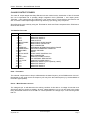
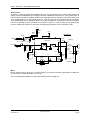
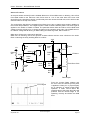
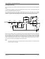
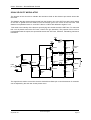
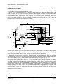
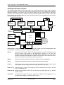
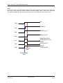
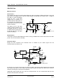
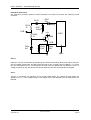
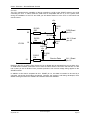
50Hz
Colour Television
DA100 and DW100
Chassis
Colour Television – DA100/DW100 Chassis
Contents
POWER SUPPLIES...........................................................................................................................1
Switch Mode Power Supply......................................................................................................1
Start up operation...........................................................................................................1
Voltage regulation ..........................................................................................................2
Over-voltage Protection..................................................................................................2
Over-current control .......................................................................................................2
Slave Processor Power Supply.................................................................................................3
Degauss Circuit........................................................................................................................4
5v Regulator ............................................................................................................................5
DA100 (59ESD7H and 66ESD7H) 4:3 chassis................................................................5
DW100 (56FW53H to 6FW54H) 16:9 chassis .................................................................6
CLASS D OUTPUT STAGES ............................................................................................................7
Tda7480 Pin Functions.............................................................................................................7
Pin 9 – Frequency ..........................................................................................................7
Pin 12 – Mute/Standby function ......................................................................................7
Audio Output............................................................................................................................8
Field Output .............................................................................................................................9
Vertical Fly-back...........................................................................................................10
VIDEO AND SYNC PROCESSOR ...................................................................................................11
Description.............................................................................................................................11
Analogue front-end.......................................................................................................11
Input Selector...............................................................................................................11
Clamping......................................................................................................................11
Automatic Gain Control ................................................................................................12
Analogue-to-Digital Converters.....................................................................................12
Digitally Controlled Clock Oscillator ..............................................................................12
Analogue Video Output ................................................................................................12
Average Beam Current Limiting....................................................................................12
Protection Circuitry .......................................................................................................12
Scan Velocity Modulation Output ..................................................................................12
PICTURE ROTATION......................................................................................................................13
SCAN VELOCITY MODULATOR ....................................................................................................14
LINE OUTPUT STAGE....................................................................................................................15
East West Circuit....................................................................................................................16
Circuit Description ........................................................................................................16
MICROPROCESSOR CONTROL ....................................................................................................17
Reset .....................................................................................................................................18
PROTECTION .................................................................................................................................19
Microprocessor.......................................................................................................................19
Audio Output ................................................................................................................19
Beam Current...............................................................................................................19
Horizontal Mute ............................................................................................................19
Video/Sync Processor ............................................................................................................20
Safety ..........................................................................................................................20
Vprot ............................................................................................................................20
Sharp Electronics (UK) Ltd
Technical Support
September 99
Colour Television – DA100/DW100 Chassis
POWER SUPPLIES
This CTV employs two power supplies, which are similar in design to previous models. The Power
Supply located on the sub-board 'PWB-C' will supply the Dolby Prologic circuit and Audio Output
Stages that are also located on PWB-C. Similar to the CS, CA10 and CW100 chassis, when this
receiver is in standby mode, the outputs from the power supplies (including the supply to the Main
Microprocessor circuit) will be muted by removal of the FET gate voltage. The Slave Processor
(IC702) performs standby and timer on/off functions, additionally in this chassis the Slave Processor
will control the degauss circuit.
SWITCH MODE POWER SUPPLY
+8v
+HT
T701
17
R715
47k
R713
560k
R714
560k
C710
47nF
D718
C718
1000
D719
C719
1000
4
To Degauss
Circuit
D712
15v
C714
82nF
R717
22k
D720
R719
220
Q702
D730
R716
0R47
Q703
C738
56pF
C713
68nF
C715
330pF
R718
18
R723
270
D716
5v6
C717
15nF
150V
C720
100
12
R766
220
6
15
D713
+16v
-16v
5
R730
82
D721
8v2
3
Q701
C711
330pF
R727
180
7
D711
C712
100pF
8
R728
180
1
R765
220
D715
R722
0R33
C718
3n3
14
2
IC705
D726
12v
R743
47k
Standby
R724
470
R750
1M
R744
47k
IC706
R745
1k8
R746
47k
START UP OPERATION
Rectified and smoothed mains voltage (+320VDC) is used to provide the start up voltage to the gate
of Q701. Current flows via R713 and R714 charging C714 (C714 earth return is via T701 secondary
winding pins 14 and 15). This allows a voltage at the gate of Q701 to rise slowly (Q701 will turn on
when the gate reaches 4.5V). D712 ensures that Q701 gate voltage will not exceed 15V, preventing
the FET being damage by voltage spikes.
When Q701 turns on, current will flow from the bridge rectifier, through T701 primary winding (pins 12
and 17), Q701 source/drain junction, returning to the bridge rectifier via, R716. The current flowing
through T701 primary will induce an e.m.f. into secondary windings
The e.m.f. produced at T701 pin 15 will flow through D715 and the collector emitter junction of the
opto-coupler (IC705), charging C713. Once the charge on C713 reaches 0.6V Q703 will turn on,
connecting Q701 gate to ground, turning Q701 off and discharging C714.
Sharp Electronics (UK) Ltd
Technical Support
September 99
Page 1
Colour Television – DA100/DW100 Chassis
At this point, the magnetic field within T701 will collapse causing the e.m.f at pin 15 to go negative
turning Q703 off.
Q701 will not turn on until sufficient charge has built up on C714. However, at this time the negative
plate of C714 is approximately -12V; due to the collapsing field within T701. This results in the time
period required to build sufficient charge on C714 to bias Q701 on increasing i.e. Q701 off time = the
time for the back 'e.m.f.' to decade to zero, plus C714 charge time form zero to 4.5V approx.).
VOLTAGE REGULATION
The feed back through the opto-coupler (IC705), provides voltage regulation. The +150V line is used
as the controlling source and a reference is provided from the +16v supply.
Increase in load
As the +150V rail falls due to an increase in load (high beam current), the trigger voltage of IC706 will
fall, increasing IC706 cathode voltage, reducing the current flowing through the LED section of IC705.
This has the effect of decreasing the conduction of the photo transistor part of IC705. This increases
the voltage drop across the collector/emitter junction; thereby increasing the time taken to charge
C713, delaying the point when Q703 turns on, turning Q701 off. Energy is transferred across T701 for
a longer period, increasing the HT rail; hence, the frequency of the power supply will fall.
Decrease in load
As the +150V rail increase due to a decreasing load (low beam current), the trigger voltage of IC706
will rise decreasing IC706 cathode voltage which increases the current flow through the LED section
of IC705. This has the effect of increase the conduction of the phototransistor within IC705. Thereby
decreasing the voltage drop across the collector/emitter junction; which will decrease C713 charge
time, advancing the point when Q703 turns off, turning off Q701 to turn on earlier. Energy is
transferred across T701 for a shorter period, decreasing the HT rail; hence, the frequency of the
power supply will increase.
It can now be seen that this is a variable frequency power supply, typically the frequency will vary
between 144kHz (no load) to 70kHz (high beam current).
OVER-VOLTAGE PROTECTION
D716 is used to prevent the secondary rails increasing beyond safe limits. If the e.m.f. at T701 pin 15
increases beyond safe limits D716 will conduct, increase the voltage across C713, thereby reducing
its charge time, turning on Q703 earlier, turning off Q701, allowing the HT rails to fall. Once the HT
starts to fall Q703 will turn off allowing the Power Supply to restart.
OVER-CURRENT CONTROL
Over current control is performed by monitoring the amount of current passing though the R716
(Q701 drain, earth return resistor). This resistor is an extremely low value, 0.47R, and Ohms Law
dictates that the current flowing through it must be proportional to the voltage across it. The base
voltage required for turning on Q702, is +0.6V then the voltage across R706 to ‘trip’ the circuit would
have to be approximately 1.2V (this includes 0.6V drop across D720). Therefore a current of 2.5amps
is required to operate the trip circuit.
The voltage developed across R716 will turn Q702 on via D713 and R719. Once Q702 turns on,
C714 will discharge rapidly, removing Q701 gate bias. Q701 will remain turn off until the current
through R716 decreases. At this point Q702 turns off allowing C714 to charge turning on Q701. If the
overload is still present then Q702 will turn on again, thus repeating the cycle. In the case of a short
circuit line output transistor the power supply will keep repeating this cycle. The HT rail and base of
Q702 (if measured with a standard DVM) would normally read zero volts and the power supply
appears not to be working. On some occasions when the short is not as heavy then a whistle may be
heard.
Sharp Electronics (UK) Ltd
Technical Support
September 99
Page 2
Colour Television – DA100/DW100 Chassis
SLAVE PROCESSOR POWER SUPPLY
This part of the circuit has changed compared to previous chassis, where this supply was derived by
means of a bridge rectifier with two additional 68k resistors and a 5v1 zener diode to limit the voltage.
This has been replaced by a series regulator circuit, which is supplied from one side of the mains, with
an earth return via the bridge rectifier.
D708 and D707 forms part of a bridge rectifier, two diodes of the main bridge rectifier are used for the
other part. Therefore, at the junction of D707 and D708 there is a 100Hz signal comprising of positive
halve cycles at mains potential. Each time this signal exceeds 47v D729 will conduct, turning on
Q717.
D734
R771
470k
D731
HT
D707
R774
470k
R775
470k
D732
15v
R703
150k
R777
47
Q715
+5v
C739
220
D710
5v1
C724
220
D733
D729
47v
R776
82k
R721
150k
R770
220
D708
R738
47k
R735
470k
R739
47k
R736
470k
Q717
Clock
Q708
Q709
R737
180k
C725
4n7
R787
47k
When Q717 turns on the gate of Q715 is taken to ground. Since this is a N Channel MOSFET Q715 is
turned off and no current will flow through this device.
During the period when Q717 is turned off Q715 will turn on allowing C739 to charge to approximately
7v which is limited to 5v by R777 and D710.
It can now be seen that the period of Q715 conduction is very short (it is only turned on when the
100Hz signal at the junction of D707 and D708 is less than 47v). Therefore, a top-up supply from the
bridge rectifier circuit comprising of D734 and D731 is added to the cathode of D710 via R721 and
R703.
The 100Hz signal at the junction Q717 and D733 is also used as a timing signal for the real time clock
within the slave processor. However, before it can be used the signal is passed through a Schmitt
Trigger circuit (Q708 and Q709) to ensure that the signal free from noise.
Sharp Electronics (UK) Ltd
Technical Support
September 99
Page 3
Colour Television – DA100/DW100 Chassis
DEGAUSS CIRCUIT
This circuit is configured to ensure that the degauss circuit will not operated unless the switch mode
power supply is operating and IC702 pin 14 = low.
A positive bias is applied to the emitter of Q714 from T701 pin 15 (rectified by D727 and limited by
D728). Via the opto-coupler; IC708. Since Q714 is a pnp device once the base is taken low compared
to the emitter, Q714 will turn on allowing current to flow through IC708 (LED Section), turning on the
triac T702, allowing current to flow through the degauss coils.
N
T702
POR701
C702
10nF
Degause
Coils
L
D728
4v7
IC708
R768
220
R763
100
Q714
From IC702
pin 14
R762
220
D727
From T701
pin15
Current will continue to flow through the degauss coils until either the PTC (POR701) has increased in
value sufficiently to cut off the current flow, or IC702 pin 14 goes high, turning of Q714, preventing
current flow through IC708, turning the triac T702 off.
Since the default condition for IC702 = low, it can be seen that the degauss circuit should now operate
each time the CTV is turned on from the main on/off switch or switched from standby to normal
operation. Whether the main processor has set up communication with the slave processor or not.
Sharp Electronics (UK) Ltd
Technical Support
September 99
Page 4
Colour Television – DA100/DW100 Chassis
5V REGULATOR
This is another new circuit, but depending on whether you are dealing with the DA100 (4:3) chassis or
DW100 (16:9) chassis will determine the exact circuit.
DA100 (59ESD7H AND 66ESD7H) 4:3 CHASSIS
The FET Q704 is a series regulator producing 5v, which is controlled by Q713. A voltage is fed-back
from the output of Q704 (junction of L705 and C723) which will control the conduction of a variable
zener diode (IC707). D723, Q705 and Q706 provide protection against excessive supply voltage.
D722
+16v
C735
150pF
C722
10nF
R707
1k5
Q713
R757
2k2
From T701
pin 1
D714
R726
22
R710
2k2
R725
10k
R706
8k2
R760
4k7
R729
4k7
Q704
C734
470
C721
470
L705
Q706
IC707
+5v
D723
2v7
R731
10k
R756
10k
Q705
C723
2200
Sharp Electronics (UK) Ltd
Technical Support
September 99
Page 5
Colour Television – DA100/DW100 Chassis
DW100 (56FW53H TO 6FW54H) 16:9 CHASSIS
For models using the DW100 chassis this regulator circuit has been replaced by an integrated circuit
(L4978D).
R748
4k7
C742
68nF
D722
11
T701 pin 1
C721
470
C743
100nF
C735
2n7
R706
20k
R747
2k7
14
+5v
IC707
C722
100nF
4
L705
13
3
C741
100nF
5,6
2
D714
This DC-DC converter will operate from a supply between 8v to 55v and produces an output voltage
of between 3v3 and 50v depending on the value of R747 (5v output R747 = 2k7). C741 connected to
pin 3 provides a soft-start routine. If pin 3 is held low then the device will not operate. The frequency
of the internal oscillator is fixed by the value of R706 and C735. Over-current and over-voltage
protection is incorporated into the design of this device.
Sharp Electronics (UK) Ltd
Technical Support
September 99
Page 6
Colour Television – DA100/DW100 Chassis
CLASS D OUTPUT STAGES
The class ‘D’ output stages that Sharp Electronics have used since the introduction of the CS chassis
are now incorporated into a specially design integrated circuit (TDA7480 = 10w output power,
TDA7481 = 15w output power and TDA7482 = 25w output power). These devices are ideal for use
with TV Audio & Field output stages where high efficiency (low energy use) is required.
Sharp Electronics are currently using the TDA7480 for Audio and Frame outputs and the TDA7481 to
drive the sub-woofer.
T DA7480 PIN F UNCTIONS
Pin No.
1
2
3
4
5
6
7
8
9
10
11
12
13
14
15
16
17
18
19
20
Name
-VCC
-VCC
-VCC
OUT
BOOTDIODE
BOOT
NC
FEEDCAP
FREQUENCY
SGN-GND
IN
ST-BY-MUTE
NC
+VCC SIGN
VREG
+VCC POW
-VCC
-VCC
-VCC
-VCC
Function
NEGATIVE SUPPLY.
NEGATIVE SUPPLY.
NEGATIVE SUPPLY.
PWM OUTPUT
BOOTSTRAP DIODE ANODE
BOOTSTRAP CAPACITOR
NOT CONNECTED
FEEDBACK INTEGRATING CAPACITANCE
SETTING FREQUENCY RESISTOR
SIGNAL GROUND
INPUT
ST-BY/ MUTE CONTROL PIN
NOT CONNECTED
POSITIVE SIGNAL SUPPLY
10V INTERNAL REGULATOR
POSITIVE POWER SUPPLY
NEGATIVE SUPPLY (De-coupled by 100nF)
NEGATIVE SUPPLY
NEGATIVE SUPPLY
NEGATIVE SUPPLY
PIN 9 – FREQUENCY
The external components on this pin will determine the base frequency of the PWM section of this IC.
Remember for the audio circuit the frequency will vary from the base frequency by the bandwidth of
the audio signal (20kHz).
PIN 12 – MUTE/STANDBY FUNCTION
The voltage at pin 12 will determine the working condition of this device. A voltage of less than 0.8v
will tell the device to switch to standby, where a voltage between 1.8v to 2.5v will result in the output
being attenuated between 60 to 80 dB. For normal operation the voltage at pin 12 should be greater
than 4v.
Sharp Electronics (UK) Ltd
Technical Support
September 99
Page 7
Colour Television – DA100/DW100 Chassis
AUDIO OUTPUT
At switch on C362 is discharged holding IC301, pin 12 low preventing any output from IC301 until
supply has been established. Once supply has been established and IC301, pin 12 is greater than 4v
then the IC301 will start to oscillate, producing a PWM signal with a frequency and a mark space ratio
which is dependant on the input signal at pin 11. L352 and C361 form a low pass filter for conversion
of the PWM signal into an analogue signal to drive the loudspeaker. A proportion of this drive signal is
fed into an averaging circuit via R358 as a protection signal i.e. if the average of the signal at the
junction of R358 and L352 is not zero then the software will switch the CTV to standby mode.
+5v
R350
10k
R351
27k
+16v
Left Channel
Q305
C362
2.2
Mute
R362
4k7
12 St-By/Mute
14
Vcc sign
7,13
N.C
Boot
6
TDA7480
C356
15nF
11
Input
R372
10k
16
Vcc pow
C357
1nF
R375
47k
-PRE
4
+
8
C360
560pF
Feedcap
IC301
5
Boot Diode
Sign-GND
C359
4n7
10
-Vcc
1,2,3,18,19,20
Freq
9
C354
100pf
200kHz
L352
-PWM
+
C353
100nF
-16v
-Vcc
17
15
Vref
R353
150
C361
470nF
R358
100k
C358
100nF
Protection
R352
12k
MUTE
During system reset or when the ‘Line Mute (HOUT)’ is present, the audio outputs will be muted due
to an increase in Q305 base bias, turning it on.
The circuit description/diagram for this mute signal is shown on page 19.
Sharp Electronics (UK) Ltd
Technical Support
September 99
Page 8
Colour Television – DA100/DW100 Chassis
FIELD OUTPUT
The operation of the field output circuit is similar to the audio with the exception that there is no mute
circuit except for C511, which will stop the circuit from operating until the +13v supply, is present.
+5v
+13v
R509
39k
Vertical
Flyback
12 St-By/Mute
R544
1k
Input
16
Vcc pow
C511
2.2
14
Vcc sign
7,13
N.C
TDA7480
11
-PRE
C524
330nF
6
L352
-PWM
+
C505
100nF
Boot
4
+
C508
560pF
8
Feedcap
IC501
5
Boot Diode
Sign-GND
10
C507
4n7
-Vcc
1,2,3,18,19,20
Freq
9
C503
100pf
R502
4k7
R515
1k2
R510
8k2
IC502
-Vcc
17
-13v
R503
1k
R511
150
15
Vref
C534
1nF
C506
100nF
Vertical
Flyback
3
Q503
Field Coils
R518
1R
C504
680nF
R533
1R
R501
150
R516
1k
1
R512
4k7
2
The PWM signal from pin 4 of the IC, is passed through a low pass filter (L352 and C504) producing a
ramp signal at the field deflection coils. This ramp waveform will vary between +13v when the scan is
at the top of the screen decreasing to –13v when the scan has reached the bottom of the screen. The
field scan coils are returned to ground via Q503. Q503 is turned on during the vertical scan period and
turn off during vertical fly-back.
IC502 will produce an error signal. This error signal is fed to the vertical drive input (IC501 pin 11), for
the purpose of linearity and amplitude correction.
Sharp Electronics (UK) Ltd
Technical Support
September 99
Page 9
Colour Television – DA100/DW100 Chassis
VERTICAL FLY-BACK
At the point where vertical fly-back is initiated Q503 turns off and Q502 turns on allowing +25v to flow
from Q502 emitter to the field scan coils. Since there is –13v on the other side of the scan coils
derived from the vertical drive signal, we effectively have 38v across the field coils, which will force the
electron beam to the top of the screen.
The vertical drive signal that is outputted from IC801 pin 31 has a negative going pulse in addition to
the normal ramp waveform. This negative pulse is used to initiate vertical fly-back. This drive signal is
applied to the emitter of Q505 via R508. The potential divider R526 and R514 will fix Q505 base
voltage so that it will only turn on during the period of the negative going pulse. Once Q505 turns on
its collector voltage will fall turning on Q507 taking its emitter to ground, which results in:
Q503 turns off due to the removal of gate bias
Q502 turns on allowing +25v at the junction of Q502 collector and the scan coils due to the action
D507 conducting secondly enabling D507 to conduct.
+25v
R504
39k
+5v
R526
4k7
R547
3k9
D508
R505
2k2
Q502
Q507
R506
120
Q505
VProtect
R528
100k
R514
390
R508
680
D507
12v
C512
220nF
R517
15k
Field Scan Coils
Q503
R507
8k2
Drive
Field Output
V Prot Signal
From the Junction Q502 collector and
the scan coils the vertical fly-back pulse
is applied to IC801 pin 11 (Vprot Signal)
as an indicator of vertical output stage
operation. If IC801 cannot detect the
negative edge of this pulse the IC801 will
presume that the vertical stage is not
operating correctly and blank the RGB
drive.
Sharp Electronics (UK) Ltd
Technical Support
September 99
Page 10
Colour Television – DA100/DW100 Chassis
VIDEO AND SYNC PROCESSOR
This IC is a member of the ‘Micronas’ VDP 31xxB IC family, which are high-quality video processors
Allowing the economic integration of features in all classes of TV sets. The VDP 31xxB family is
based on functional blocks contained in the two previous chips form Micronas:
VPC 3200A Video Processor
DDP 3300A Display and Deflection Processor
VDP 31xxB contains the entire video, display, and deflection processing for 4:3 and 16:9 CTV’s
operating at either 50 or 60Hz featuring:
2H adaptive Comb-filter
Scan Velocity Modulator.
1H Comb-filter
Colour Transient Improvement.
RGB Insertion
Tube Control
Programmable RGB Matrix
4 composite inputs (one for S-VHS)
Composite video & sync output
Horizontal scaling (0.25 to 4)
Panorama vision
Black level expander
Dynamic peaking
Soft-limiter (gamma correction)
Picture frame generator
High-performance H/V deflection
Separate ADC for tube measurements
EHT compensation
One 20.25 MHz crystal (for all systems), few external components
Embedded RISC controller (80 MIPS)
I 2 C-Bus Interface
Single 5 V power supply
DESCRIPTION
ANALOGUE FRONT-END
This block provides the analogue interfaces to all video inputs and mainly carries out analogue-to
digital conversion for the following digital video processing.
Most of the functional blocks in the front-end are digitally controlled (clamping, AGC, and clock-DCO).
The control loops are closed by the Fast Processor (‘FP’) embedded in the decoder.
INPUT SELECTOR
Up to five analogue inputs can be connected. Four inputs are for input of composite video or S-VHS
luma signal. These inputs are clamped to the sync back porch and are amplified by a variable gain
amplifier. One input is for connection of S-VHS chrominance signal. This input is internally biased and
has a fixed gain amplifier.
CLAMPING
The composite video input signals are AC coupled to the IC. The clamping voltage is stored on the
coupling capacitors and is generated by digitally controlled current sources. The clamping level is the
back porch of the video signal. S-VHS chroma is also AC coupled. The input pin is internally biased to
the centre of the ADC input range.
Sharp Electronics (UK) Ltd
Technical Support
September 99
Page 11
Colour Television – DA100/DW100 Chassis
AUTOMATIC G AIN CONTROL
A digitally working automatic gain control adjusts the magnitude of the selected base-band by +6/–4.5
dB in 64 logarithmic steps to the optimal range of the ADC. The gain of the video input stage including
the ADC is 213 steps/V with the AGC set to 0 dB.
ANALOGUE-TO-DIGITAL CONVERTERS
Two ADCs are provided to digitise the input signals. Each converter runs with 20.25 MHz and has 8
bit resolution. An integrated band-gap circuit generates the required reference voltages for the
converters.
DIGITALLY CONTROLLED CLOCK OSCILLATOR
The clock generation is also a part of the analogue front end. The crystal oscillator is controlled
digitally by the control processor; the clock frequency can be adjusted within ±150 ppm.
ANALOGUE VIDEO OUTPUT
The input signal of the Luma ADC is available at the analogue video output pin. A source follower
must buffer the signal at this pin. The output voltage is 2 V, thus the signal can be used to drive a 75Ω
line. The magnitude is adjusted with an AGC in 8 steps together with the main AGC.
AVERAGE BEAM CURRENT LIMITING
The average beam current limiter (BCL) uses the sense input for the beam current measurement. The
BCL uses a different filter to average the beam current during the active picture. The filter bandwidth
is approximately. 2 kHz.
The beam current limiter has an automatic offset adjustment that is active two lines before the first
cut-off measurement line.
The beam current limiter allows the setting of a threshold current. If the beam current is above the
threshold, the excess current is low-pass filtered and used to attenuate the RGB outputs by adjusting
the white-drive multipliers for the internal (digital) RGB signals, and the analogue contrast multipliers
for the analogue RGB inputs, respectively.
The lower limit of the attenuator is programmable, thus a minimum contrast can always be set. During
the CRT measurement, the ABL attenuation is switched off. After the white drive measurement line it
takes 3 lines to switch back to BCL limited drives and brightness.
PROTECTION CIRCUITRY
‘Vertical fly-back’ and the ‘Safety’ inputs provide picture tube and drive stage protection.
Vertical fly-back;
This pin searches for a negative edge in every field, otherwise the RGB
drive signals are blanked. Drive shutoff during fly-back: this feature can be
selected by software.
Safety;
Input pin: this input has two thresholds. Between zero and the lower
threshold, normal functioning takes place. Between the lower and the
higher threshold, the RGB signals are blanked. Above the higher
threshold, the RGB signals are blanked and the horizontal drive is shut off.
Both thresholds have a small hysteresis. The main oscillator and the
horizontal drive circuitry are run from a separate (standby) power supply
and are already active while the TV set is powering up.
Note:
In the DA100 and DW100 chassis the standby supply pin is connected to VCC.
SCAN VELOCITY MODULATION OUTPUT
This output delivers the analogue SVM signal. The D/A converter is a current sink like the RGB D/A
converters. At zero signal level the output current is 50% of the maximum output current.
Sharp Electronics (UK) Ltd
Technical Support
September 99
Page 12
Colour Television – DA100/DW100 Chassis
PICTURE ROTATION
Due to the width of a 16:9 CRT the horizontal tilt of the picture can be influence by external magnetic
fields.
To overcome this problem, an extra coil is fitted around the CRT, which is connected between the
junction of Q1603/Q1604 emitter and ground.
The microprocessor (IC1001) will output a PWM signal from pin 55. This signal is then passed
through a LPF and fed to an error amplifier (IC601). The output from this error amp can swing from a
positive to a negative voltage depending on the mark space ratio of the PWM signal from IC1001.
+13v
C1612
220
R1615
1M
1kHz PWM
IC1001, pin 55
R1620
10k
R1619
100k
C1608
10
R1617
2k2
D1607
2v4
C1611
10nF
R1616
100k
Q1603
R1622
470
IC1601
R1618
100k
+
R1621
100
R1624
100
Tilt Coils
Q1604
C1609
10
C1610
100nF
R1623
100
-13v
C1613
220
Under normal conditions (CRT is not effected by external magnetic fields) there will be no output from
the error amplifier, therefore, both Q1603 and Q1604 are turned off causing no current to flow through
the coil around the CRT neck. However if the output from the error amplifier is positive then Q1603
will turn on allowing current to flow from the +13v rail, through the coil to ground. If the error amplifier
output is negative going then Q1604 will turn on, allowing current to flow from ground to the –13v rail.
The end user has control of this adjustment via the picture menu.
Note
The location of this circuit can vary between 66cm models (Located on CRT base) and 76cm
models (located on sub PWB).
Sharp Electronics (UK) Ltd
Technical Support
September 99
Page 13
Colour Television – DA100/DW100 Chassis
SCAN VELOCITY MODULATOR
The purpose of this circuit is to maintain the luminance level as the electron spot moves across the
CRT face.
The distance that the electron beam travels from the electron gun to the CRT face at the outer edges
of the CRT is greater than the distance from the electron gun to the centre of the CRT face. This
distance is emphasised more on 16:9 CRT’s than 4:3 CRT’s with deflection angles of 110°
This result in the intensity of the electron spot varying as it travels across the CRT face. To overcome
this a coil is placed around the CRT neck, close to the gun assembly. The purpose of this coil is to
increase/decrease the speed, the spot travels across the CRT face, therefore, maintaining luminance
transitions.
140v
+12v
R5425
470
R5415
82
Q5405
R5431
390
R5432
33
R5433
100
R5413 C5408
10
68nF
R5412
47
IC801
pin 34
Q5410
+5v
Q5412
R5434
1k
Q5406
R5435
220
R5416
3k3 R5417
0
R5423
3R3
Q5407
SVM Coils
R5414
10
Q5411
R5410
0
C5409
68nF
R5418
3k3
Q5408
R5419
82
R5421
3R3
R5411
0
The signal that is used to control this circuit is derived from IC801 pin 34 and the amount of correction
can be adjusted by the end user via the picture menu.
Sharp Electronics (UK) Ltd
Technical Support
September 99
Page 14
Colour Television – DA100/DW100 Chassis
LINE OUTPUT STAGE
As in previous chassis a transformer-less driver circuit has been used, with the driver stage obtaining
it’s run voltage from the fly-back transformer, T601.
At switch on +8v from the power supply is applied to Q603 collector via R605 and Q602 collector via
R628 and R608. At the same time –16v is applied to Q602 emitter via R619. Horizontal drive from
IC801 is applied to the base of Q603, This will cause Q603 to switch, which in turn switches the line
output transistor Q601, producing an e.m.f on pins 6 and 10 of the fly-back transformer T601. The
e.m.f at pin 10 is rectified by D611 to produce the positive run voltage and the e.m.f at pin 6 is
rectified by D610 to produce the negative run voltage.
D611
+150v
L606
R608
1k
+8V
R617
22
Q601
L609
C610
27nF
Q603
Line
Drive
R612
22
R601
3k9
R642
470
C601
12nF
Focus
7
+150v
(CRT Base)
R628
1k
EHT
2
D621
R605
470
R607
12k
R623
1
Screen
3
13
D603
8
ABL
10
D604
East/West Circuit
1
4
R617
22
6
+25v
5 9
+13v
Q602
R624
D610 5R6
R619
560
HFB
D510
D609
F602
D608
F601
-13v
C607
330
-16v
With this type of driver circuit, it is essential that the circuit is started softly, otherwise transient pulses
can damage the line output transistor. This is achieved by doubling the horizontal drive frequency;
which effectively reduces Q601 on time, until the run voltage has been established.
In addition to producing the EHT, focus, screen voltage and horizontal scan from the fly-back
transformer T601, the +/-13v rails for the field output are produced at pins 5 and 9. D609 rectifies the
e.m.f at pin 9 producing the +13v and D608 rectifies the e.m.f at pin 5 producing the –13v.
Horizontal fly-back pulses (HFB) from pin 1 is fed to IC801 for both timing purposes and safety
(prevents excesses EHT), HFB is also rectified by D610 to produce +25v for vertical fly-back. From
the primary winding (pin 7) the HT is stepped up and rectified by D621 to produce the HT required by
the CRT drive circuit. Finally a negative going voltage is fed from pin 8 to the protection circuit. This
voltage represents the beam current. The greater the beam current (Bright Raster) the greater this
voltage would be in a negative direction. This negative voltage is then fed to the IC1001 pin 95 via
D622 and Q606. Once this voltage has exceeded safe working levels IC1001 pin 95 will go low
switching the CTV to standby.
Sharp Electronics (UK) Ltd
Technical Support
September 99
Page 15
Colour Television – DA100/DW100 Chassis
EAST WEST CIRCUIT
In addition to the normal function of an East West correction circuit used with 4:3, 110° CRT, with a
wide screen CTV correction has to be allowed for the different types of scanning modes.
16:9 CTV generally has three scanning modes, 4:3, 14:9 and 16:9, additionally the 16:9 scanning
modes has three variants, Full, Panama and Cinema. Full mode is used to stretch a picture which is in
4:3 format and contains fast moving action (motor racing), therefore, it does not matter if the line
linearity is not constant across the screen. Panama is similar to full mode but this time the action is
slow or even stationary (news programs), therefore, your eye would pickup on any variation in
linearity. To overcome this the linearity in the centre of the screen is kept constant and the edges of
the picture are stretched to fill the screen. Cinema mode is intended for use with pictures that are in
true 16:9 format.
R555
100k
+150v
D506
R613
2k2
C518
10pF
R527
1k
R525
5k6
R524
1k
Q501
Line
Drive
Q601 (c)
+5v
+5v
R519
100k
Scan Coils
R556
10k
C514
47nF
R610
1
+
C620
2.2
Q506
R525
10k
D503
EW Drive
D613
C613
560nF
C619
2.2
L605
L603
C611
1
RA611
3k3
L604
IC503
Diode Modulator
CIRCUIT DESCRIPTION
IC503 is a switching amplifier with integrated line pulses being fed to one input from the line driver
circuit via Q501 and an East West parabolic signal from IC801 to the other input. This will produce a
PWM signal running at line frequency and the width of the pulses will be determine by the East West
parabolic signal.
This signal is then passed a driver circuit (Q506, class ‘d’ biased), low passed filtered (L603, C610) to
the diode modulator (D603 and D604). Additionally from L603 the signal is fed to one end of a centre
tap coil (L604) via C611. The other of L604 is connected to ground with the centre tap connected to
the line linearity circuit. Therefore the line linearity can now be adjusted by the East West Parabolic
signal.
Sharp Electronics (UK) Ltd
Technical Support
September 99
Page 16
Colour Television – DA100/DW100 Chassis
MICROPROCESSOR CONTROL
The microprocessor (CPU) is at the hart of this CTV, communicating with all other area via various
data buses. Similar to the CS, CA10 and CW100 chassis this CPU is not operating during standby,
therefore contained in the primary side of the power supply there is a slave processor. This slave
processor has a volatile memory, therefore each time power is applied to this CTV the switch mode
powers supply has to start enabling the slave processor program to be downloaded from the OTProm
before switching to standby.
I2S Bus
Dolby
Processor
Multi-Sound
Processor
Video/Sync
Processor
IF
Tuner
IC2028
I2C Bus (1)
AFT-1
AFT-2
Slave
Processor
OTP
NVM
(eeprom)
IC1001
(CPU)
Main Reset
Reset out (1)
Reset out (2)
AV Link Data
AV Link Clock
Protection
I2C Bus (2)
M3 Bus
NVM
(eeprom)
Page
Store
MegaText
PARALLEL BUS Communication between the CPU and the OTProm (one time programmable read
only memory). This device contains the software (operating system)
2
2
I2C BUS
There are two I C buses, I C(2) communicates between the NVM’s (eeprom), these
devices contains data relating to all adjustments, whether it is an end user
2
adjustment, service adjustment or an automatic setting performed by the CPU. I C(1)
provides serial data communications between the CPU and Tuner, Video Processor,
Multi Sound Processor and the Dolby Processor (if fitted).
M3 BUS
Data communication between CPU and the teletext processor (MegaText)
SLAVE
Data bus to the slave processor an a data us from the slave processor.
RESET IN
Main system reset, this will operate each time the main switch mode powers supply
starts. Reset is a state change from low to high generated by IC1005.
RESET OUT (1) IC801 reset (low). If IC801 is not reset then the line oscillator will not function. This will
only occur after reset in.
RESET OUT (2) Resets all other areas of this CTV, this will only occur after reset out (1). Teletext
reset is inverted.
PROTECTION
If the CPU pin 96 goes low the CTV will switch to standby. This is trigged by one of
the audio output stages or excessive beam current.
Sharp Electronics (UK) Ltd
Technical Support
September 99
Page 17
Colour Television – DA100/DW100 Chassis
RESET
It can be seen from the diagram below that all of the reset signals are a change in state, either form
low to high or high to low. The order of events is as shown, supply, reset in, reset out (1), Reset out
(2). The line oscillator will not start until reset out (1) has occurred and the HOUT pulse = zero
3v3
Low
Reset in
Low
Reset out (1)
Low
Reset out (2)
Low
Low
MegaText Reset
From Reset out (2)
Low
HOUT
IC1001 pin 57
Low
PROT
IC1001 pin 95
Line Drive
Start
Power Supply
Start
Sharp Electronics (UK) Ltd
Technical Support
September 99
Page 18
Colour Television – DA100/DW100 Chassis
PROTECTION
MICROPROCESSOR
AUDIO OUTPUT
The outputs from all of the audio output stages are fed to the base of Q303 and Q304. C377 and
R361 form an averaging circuit. Since the audio signals are basically sine waves the d.c. voltage at
the base of these transistors
+5v
should be zero. If this base
voltage was to increase in a
R1021
positive direction Q303 will turn
4k7
D301
on, removing the biased from
Protection
IC1001 pin 95, and the CTV will
IC1001 pin 95
Q303
switch to standby.
Q302
Q606
The same is true if the base
voltage increase negatively, this
time Q304 will turn on, turning
on Q302 causing IC1001 pin 95
to fall and the CTV will again
switch two standby.
R360
10k
Q304
Audio
-16v
C377
10
R361
10k
C644
2200
D622
27v
R615
5k6
ABL
(T601 pin 8)
BEAM CURRENT
If the beam current increase D622 will conduct, turning on Q606 which removes the bias from IC1001
pin 95. The CTV will switch to standby
HORIZONTAL MUTE
During the boot sequence the horizontal drive is inhibited by the HOUT signal from the
microprocessor (IC1001 pin 57).
R1005
4k7
5v
1
C1028
100nF
3v3
Q1004
R1044
10k
IC1005
3
2
Mute
D1009
C1033
68nF
Line Drive
Main
Reset
R1047
10k
Q602
R626
4k7
R1049
10k
3v3
HOUT
IC1001 pin 57
Its function is to remove the line drive by turning on Q607, thus placing short between the horizontal
drive signal and ground, at the same time this HOUT pulse will cause the audio mute circuits to
activate, preventing any noise from the speakers.
Additionally HOUT signal will occur when the microprocessor can not communicate with the other
devices connected to the I²C buses
Sharp Electronics (UK) Ltd
Technical Support
September 99
Page 19
Colour Television – DA100/DW100 Chassis
VIDEO/SYNC PROCESSOR
The video/sync processor (IC801) contains protection circuit that can monitor the scanning circuits
operation.
D617
24v
D615
12
R615
1k
Safety
C617
100nF
HFB
+5v
R620
1k
IC801
Q608
HFB
13
11
D618
4v7
C643
10nF
R644
220
Vprot
SAFETY
IC801 pin 12, EHT is calculated by measuring the rectified horizontal fly-back pulse. D615 and C617
are the rectifier components, and D617 limits the bias at pin 12 (sets normal conditions, >1v) There
are two thresholds once the first threshold has been met the RGB drives are blanked, if the d.c.
voltage continues to rise and passes the second threshold, then the horizontal drive is stopped.
VPROT
This pin is monitoring the operation of the vertical output stage. The vertical fly-back pulses are
applied to pin 11. If the negative edge of this signal cannot be detected then the RGB drives are
blanked.
Sharp Electronics (UK) Ltd
Technical Support
September 99
Page 20
Colour Television – DA100/DW100 Chassis
A V Link
This CTV chassis has the capability of directly controlling a VCR via the SCART socket or the VCR
controlling the CTV. In either chase the VCR must be compatible with the ‘A V Link’ system, also
during the installation of the CTV and VCR you will decide whether it is the CTV or VCR which has
overall control.
+5v
R1032
27k
R1023
220
92
RGB Scart
pin 10
D1003
IC1001
16
R1033
10k
D411
5v6
AV-1 Scart
pin 10
Q1005
+5v
R1025
10k
21
R1035
4k7
Service Data
AV-1 Scart
pin 12
Data from the CTV to VCR is from IC1001 pin 16 via Q1005 and is outputted from pin 10 either AV-1
or RGB SCART sockets. Data from VCR is from the same SCART connection but this time it is fed
into IC1001 pin 92 via D1003. D411 provides protection from excess voltage being applied to the
SCART sockets.
In addition to this data is outputted at AV-1 SCART pin 12, this data is intended to be read by a
computer, enhancing fault finding procedures. Currently this system is still being developed, more
details will be given when the software and interface becomes available.
Sharp Electronics (UK) Ltd
Technical Support
September 99
Page 21
Colour Television – DA100/DW100 Chassis
Sharp Electronics (UK) Ltd
Technical Support
September 99
Page 22