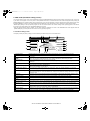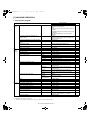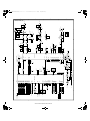
1
[00]COVER.fm 1 ページ
2004年10月26日 火曜日 午後3時41分
CODE : 00ZARFX12/A1E
LASER PRINTER OPTIONS
FAX EXPANSION KIT
(For North America)
MODEL
AR-FX12
OPTION
AR-MM9
CONTENTS
[1]
PRODUCT OUTLINE . . . . . . . . . . . . . . . . . . . . . . . . . . . . . . . . 1 - 1
[2]
CONFIGURATION . . . . . . . . . . . . . . . . . . . . . . . . . . . . . . . . . . 1 - 1
[3]
SPECIFICATIONS . . . . . . . . . . . . . . . . . . . . . . . . . . . . . . . . . . 3 - 1
[4]
EXTERNAL VIEWS AND INTERNAL STRUCTURES . . . . . . . 4 - 1
[5]
UNPACKING AND INSTALLATION. . . . . . . . . . . . . . . . . . . . . . 5 - 1
[6]
SIMULATIONS, FAX SOFTWARE SWITCH. . . . . . . . . . . . . . . 6 - 1
[7]
MACHINE OPERATION . . . . . . . . . . . . . . . . . . . . . . . . . . . . . . 7 - 1
[8]
ELECTRICAL SECTION . . . . . . . . . . . . . . . . . . . . . . . . . . . . . 8 - 1
Parts marked with “ “ are important for maintaining the safety of the set.
Be sure to replace these parts with specified ones for maintaining the safety and performance of the set.
SHARP CORPORATION
This document has been published to be used for
after sales service only.
The contents are subject to change without notice.
[co]CONTENTS.fm
1 ページ
2004年10月26日 火曜日 午後3時41分
CONTENTS
[1] PRODUCT OUTLINE . . . . . . . . . . . . . . . . . . . . . . . . . . . . 1-1
[6] SIMULATIONS, FAX SOFTWARE SWITCH
1. Entering the simulation mode . . . . . . . . . . . . . . . . . . . . 6-1
[2] CONFIGURATION . . . . . . . . . . . . . . . . . . . . . . . . . . . . . . 1-1
2. Switching the simulation mode . . . . . . . . . . . . . . . . . . . 6-1
3. Canceling the simulation mode . . . . . . . . . . . . . . . . . . . 6-1
4. Simulation list . . . . . . . . . . . . . . . . . . . . . . . . . . . . . . . . 6-1
[3] SPECIFICATIONS
1. FAX function . . . . . . . . . . . . . . . . . . . . . . . . . . . . . . . . . 3-1
[4] EXTERNAL VIEWS AND INTERNAL STRUCTURES
1. Operation panel . . . . . . . . . . . . . . . . . . . . . . . . . . . . . . 4-1
2. FAX mode (Condition setting screen). . . . . . . . . . . . . . 4-2
3. PWB . . . . . . . . . . . . . . . . . . . . . . . . . . . . . . . . . . . . . . . 4-4
5. Detail of simulations . . . . . . . . . . . . . . . . . . . . . . . . . . . 6-4
6. FAX software switch . . . . . . . . . . . . . . . . . . . . . . . . . . . 6-25
[7] MACHINE OPERATION
1. Key operator program . . . . . . . . . . . . . . . . . . . . . . . . . . 7-1
2. Originals that can be faxed . . . . . . . . . . . . . . . . . . . . . . 7-2
3. Own number sending . . . . . . . . . . . . . . . . . . . . . . . . . . 7-3
4. Quick On-line . . . . . . . . . . . . . . . . . . . . . . . . . . . . . . . . 7-3
[5] UNPACKING AND INSTALLATION . . . . . . . . . . . . . . . . . 5-1
5. Trouble codes . . . . . . . . . . . . . . . . . . . . . . . . . . . . . . . . 7-4
[8] ELECTRICAL SECTION
1. Block Diagram . . . . . . . . . . . . . . . . . . . . . . . . . . . . . . . . 8-1
2. Actual Wiring Diagram . . . . . . . . . . . . . . . . . . . . . . . . . 8-2
3. Circuit Diagram . . . . . . . . . . . . . . . . . . . . . . . . . . . . . . . 8-3
4. Part Layout . . . . . . . . . . . . . . . . . . . . . . . . . . . . . . . . . . 8-19
[01]OUTLINE ・ CONFIGU.fm
1 ページ 2004年10月26日 火曜日 午後3時42分
[1] PRODUCT OUTLINE
This unit provides the FAX function and the PC-FAX function when installed to the following machines:
Machines to install this unit :
•AR-M355U/M455U
•AR-M351U/M451U
•AR-M355N/M455N
•AR-M351N/M451N
[2] CONFIGURATION
Extended memory
<AR-MM9>
* Installed to FAX I/F PWB.
FAX I/F PWB
*1
FAX Interface cable
FAX-BOX unit
<AR-FX12>
*1) Installed to the machine MFP controller PWB.
AR-FX12 PRODUCT OUTLINE • CONFIGURATION 1-1
[03]SPECIFICATIONS.fm
1 ページ
2004年10月26日 火曜日 午後3時42分
[3] SPECIFICATIONS
F. Plural destinations specifications
1. FAX function
A. Mode
Scanner (Scan to E-mail, Scan to Sharpdesk, Scan to FTP, Scan to
HDD), FAX, Internet FAX
B. Support system
Mode
Support server
Scanner
SMTP Server
FTP Server
Internet FAX
POP Server
SMTP Server
ESMTP Server
FAX
---
C. Support image
Mode
Fail system
Compression
system
Scanner
TIFF, PDF
• No
compression
• G3(First
dimension) *1
• G4 *2
Internet FAX
FAX
TIFF-F, TIFF-FX --MH, MMR
MH, MR, MMR,
JBIG
*1) G3 (First dimension) = MH(Modified Huffman)
*2) G4 = MMR (Modified MR)
Scanner
Internet FAX
FAX
Specified by one-touch, group, or direct destination
input (*).
U model: Group, interface broadcast, total 100 items
N model: Group, interface broadcast, total 5000 items
O
(FTP/Desktop:
Broadcast is
disabled.)
Sequential send --request
FAX
O
) are for U model
Mode
Scanner
Internet FAX
Corresponds to 256 gradations.
O
* Direct destination input: Input by 10-key or soft keyboard other than
one touch.
* For broadcast including FAX , it is the FAX resolution.
* For broadcast of the internet FAX and the scanner, it is the internet
FAX resolution.
* The compression type of broadcast conforms to the key operation
setting.
G. Function Values in (
D. Image process
Mode
Half-tone
reproduction
Density
adjustment
Image quality
selection
Resolution
(Differs
depending on
the file type/
send method).
Mode
Destination
specifications
Number of items
which can be
registered by
direct
destination input
Broadcast send
Scanner
Send
Memory send
function
Automatic + 5 steps
Half-tone ON/OFF (*) is inhibited.
On-hook
--Memory
send is
performed
when the
upper limit
value is set.
Internet FAX
FAX
O
---
O
Quick online send ---
O
Direct send
---
Only when
on-hook
Automatic
reduction send
---
O
A3
A3
B4
Rotational send
O
E. Destination specification Values in ( ) are for the U model
Zoom send
O (Only fixed size
fixed size. Rotation
is disable for some combinations.)
Mode
LDAP
Destination
specifications
One-touch
destination
registration
items
Group
Recall
mode
Error
---
O
Busy
---
---
200 x 200dpi*
200 x 100dpi*
300 x 300dpi
200 x 200dpi
400 x 400dpi
200 x 400dpi
600 x 600dpi
400 x 400dpi
---
600 x 600dpi
Normal text
(203.2x97.8dpi)*
Fine
(203.2 x 195.6dpi)
Super fine
(203.2 x 391dpi)
Ultra fine
(406.4 x 391dpi)
---
Scanner
Internet FAX
FAX
O (Can be registered as one-touch address.)
Specified by input of one-touch, group, and direct
destination.
Total Max. 999 (500) items.
Sub total of 200 (100) items (FTP and desktop) of
them
O 500 (300) items can be registered as one-touch
dial and direct input.
Program
O (8 items)
Direct
Soft keyboard
Input by 10-key,
destination input
# key, * key
Chain dial
--Common with
(Direct
pause, up to 64
destination
digits
input)
Resend
Calls the previous destination.
Reduction
Calls the destination registration number by 10-key
destination
input.
selection
B4
A4
A4
O
Number of times and time are set by the
key operations.
Book document
send
O
Long size
document send
O
O
File division send O
---
Send size
limitation
O
O
Number of items Max. 999 items (500)
of senders which
can be registered
Receive Automatic receive --function Manual receive
--Memory receive
O
O
---
O
Fixed size
--reduction receive
O
Specified size
zoom receive
---
Rotational receive ---
AR-FX12 SPECIFICATIONS 3-1
O
Max. 800mm
O
---
[03]SPECIFICATIONS.fm
2 ページ
2004年10月26日 火曜日 午後3時42分
Mode
Scanner
Receive Division receive
function
Internet FAX
FAX
---
Conditions setting by key
operation
Duplex receive
---
Conditions setting by key
operations
2 in 1 receive
---
Address/domain
specification
receive enable
---
O (50 items) ---
Address/domain
specification
receive disable
---
O (50 items) Specified
number only
Mode
Other
External TEL
connection
remote
---
O
Answering TEL
connection
---
X (PAT
counter
measure)
Transfer function
when output is
disable
---
Automatic boot
mode
---
O
Special Time specification O
function Paling receive
---
Scanner
PC send
---
Mode
Electrical
transmission
time
Scanner
Modem speed
---
Mutual
transmission
Communication
line
---
---
O
---
O
O
ECM
Cover function
---
---
X
I. Record size
Sender print
---
O
Page division
O
Page connection
X
Confidential
(Remote
machine)
---
Interface
broadcast
specification
---
Large scale
document mode
O
Center erase
O
2 in 1
O
Card shot
Report/
List
Communication
function report list
Address/TEL
number table
Mode
Max. record
width
Record size
Scanner
Internet FAX
293mm
---
A3 - A5,11" x 17" - 5.5" x 8.5"
O (F code
system)
Mode
Sub address
Pass code
O
O
O
O
ID • Sender
address table
---
Sender table
O (Sender
registration
table)
Confidential box
check table
---
O (Integrated
with the
memory box
table).
Interface group
table
---
O (Integrated
with the
memory box
table).
Program table
O
X
Listed on the key operation
list.
AR-FX12 SPECIFICATIONS 3-2
FAX
2sec range
(Super G3/JBIG)
6 sec range
(G3 ECM)
33.6kbps
2.4kbps
Automatic
Fall back
Super G3 / G3
---
J. F code communication
Group table
PC-FAX
Public telephone
line (PSTN),
Private branch
exchange
(PBX), F net
O
O (F code
system)
O
X
Internet FAX
---
---
X
PC-iFAX
H. Transmission system
---
O
O (FAX
mode only)
--In case of an error, an output may be
made.
---
Edge erase
FAX
Memory content
cleat notification
table
Bulletin board
send
Send message
Internet FAX
Report/ Send reservation X
List
table
function Memory box table ---
Scanner
-----
FAX
Internet FAX
FAX
O
O
[04]ETERNALVIEWS.fm 1 ページ
2004年10月26日 火曜日 午後3時42分
[4] EXTERNAL VIEWS AND INTERNAL STRUCTURES
1. Operation panel
Model
Key name
Description in this manual
AR-M355N/
AR-M455N
Described in the configuration where the
optional fax expansion kit (AR-FX12) is
installed on the AR-M355N/AR-M455N models.
AR-M355U/
AR-M455U
No functions related to document filing or
Internet fax reception are described in this
manual.
1 Touch panel
(following page)
2
3
4
5
6
7
8
• Messages and keys appear in the touch panel. Touch the displayed keys to select functions and enter settings.
• When a key in the touch panel is touched, a beep sounds and the key is highlighted.
• Keys that cannot be selected in a screen are grayed out. If touched, a double-beep will sound to alert you that the key cannot
be selected.
Mode select keys Use these keys to change modes.
[IMAGE SEND]
Press to switch to fax mode. The main screen of fax mode will appear. The screen that appears when this key is selected can
key
be changed with "Default display settings" in the key operator programs.
Numeric keys
Use to enter fax numbers, sub-addresses, passcodes, and numerical settings.
[C] key (clear key) Use to clear a mistake when entering fax numbers, sub-addresses, passcodes, and numerical settings. One digit is cleared
each time you press the key.When an original is being scanned, this key can also be used to cancel scanning.
[CA] key
Use to cancel a transmission or programming operation. When this key is pressed, the operation is canceled and you return to
(clear all key)
the main screen described on the following page. This key is also used to cancel resolution, paper size and special mode
settings.
[ ] key
This is used to produce tone signals when you are on a pulse dial line.
[START] key
Press to begin scanning an original for fax transmission.
AR-FX12 EXTERNAL VIEWS AND INTERNAL STRUCTURES 4-1
[04]ETERNALVIEWS.fm 2 ページ
2004年10月26日 火曜日 午後3時42分
2. FAX mode (Condition setting screen)
The condition settings screen of fax mode is displayed by pressing the [IMAGE SEND] key while the document filing mode (printer mode), copy mode,
or job status screen appears in the touch panel. In the explanations that follow, it is assumed that the initial screen that appears after pressing the
[IMAGE SEND] key is the condition settings screen (shown below). If you have set the display to show the address book screen (following page) when
the [IMAGE SEND] key is pressed, touch the [CONDITION SETTINGS] key in the address book screen to display the condition settings screen.
"Default display settings" in the key operator programs can be used to select whether the condition settings screen (below) appears or the address
book screen (next page) appears when the [IMAGE SEND] key is pressed.
• When the network scanner option is installed, you can select whether the "E-MAIL/FTP" screen or the "INTERNET FAX" screen appears when the
[IMAGE SEND] key is pressed (the selection is made in the key operator programs).
A. Condition setting screen
The display is initially set (factory setting) to show the following condition setting screen as the initial screen.
READY TO SEND.
AUTO
EXPOSURE
SPEAKER
RESEND
FAX
MODE SWITCH
ADDRESS BOOK
ADDRESS REVIEW
STANDARD
RESOLUTION
SPECIAL MODES
SUB ADDRESS
AUTO
ORIGINAL
1
2
3
4
5
6
7
8
9
10
11
12
13
14
15
16
17
FILE
AUTO RECEPTION
FAX MEMORY:100%
QUICK FILE
Message display
[MODE SWITCH] key
Messages appear here to indicate the current status of the machine. The icon at left indicates fax mode.
Use this key when the network scanner option is installed to switch between the "E-MAIL/FTP" and "INTERNET
FAX" screens
[
] key (Speed dial key) When a one-touch dial key or group key is stored in the address book, the machine automatically assigns it a 3-digit
number. This key and the Speed Dial number can be used to abbreviate the transmission procedure.
[SPEAKER] key
Touch the [SPEAKER] key to dial and transmit a fax manually.
During dialing it changes into the [PAUSE] key, and after pressing the [SUB ADDRESS] key it changes into the
[SPACE] key.
[RESEND] key
Touch this key to redial the number most recently dialed with the numeric keys or a one-touch dial key. After dialing,
this key changes into the [NEXT ADDRESS] key.
[ADDRESS BOOK] key
Touch this key to display the address book screen (next page). Touch this key when you want to use an auto-dial
number (one-touch dialing or group dialing).
[ADDRESS REVIEW] key
When performing a broadcast transmission, touch this key to check your selected destinations. The selected
destinations will appear and any unneeded destinations can be deleted.
[SPECIAL MODES] key
Touch this key to select one of the following special functions:
•Edge erase •Dual page scan •Timer transmission •2in1 •Card shot •Job build mode •Polling •Memory box •Program
•Transaction report
[FILE] key*
Touch this key to store a document image that you are transmitting in the hard disk (this includes selecting a user
name, file name, and location).
[QUICK FILE] key*
Touch this key to store a document image that you are transmitting in the temporary storage folder.
Memory and reception mode This shows the amount of fax memory that is free and the currently selected reception mode.
display
[SUB ADDRESS] key
Touch this key to enter a sub-address and passcode when using F-code transmission.
Two-sided scanning icon
Icons appear here when you touch the [ORIGINAL] key and select two-sided scanning. The icons can be touched to
display
open function selection screens.
[ORIGINAL] key
Touch this key when you wish to manually set the size of the original to be scanned or scan both sides of the
original.
[RESOLUTION] key
Touch this key to change the resolution setting for the original to be scanned. The selected resolution setting will be
highlighted above the key. The initial factory setting is [STANDARD].
[EXPOSURE] key
Touch this key to change the exposure setting for the original to be scanned. The selected exposure setting will be
highlighted above the key. The initial factory setting is AUTO.
Special mode icon display
When a special mode such as polling or dual page scan is selected, a special mode icon appears here.
* Can only be used on the AR-M355N/AR-M455N. The AR-M355U/AR-M455U models do not have this function.
AR-FX12 EXTERNAL VIEWS AND INTERNAL STRUCTURES 4-2
[04]ETERNALVIEWS.fm 3 ページ
2004年10月26日 火曜日 午後3時42分
B. Address book screen (alphabetically ordered)
The screen below appears initially when the address book is set as the initial screen using "Default display settings" in the key operator programs.
• The screen below is the alphabetical index screen. You can also have the user index screen appear initially.
• The screen appears as shown below when the network scanner option is not installed.
READY TO SEND.
A
B
C
D
E
F
G
H
FREQUENT USE
ABCD
RESEND
SPEAKER
EFGHI
CONDITION
SETTINGS
1/2
ADDRESS REVIEW
GLOBAL
ADDRESS SEARCH
JKLMN
OPQRST
UVWXYZ
ABC
GROUP
1 One-touch key display
2
3
4
5
6
This shows the one-touch keys that have been stored on the selected "index card". The key type is indicated by
the icon at the right. One-touch keys in which a fax number is stored are indicated by a "
" icon.
The display is initially set to show 6 keys. This can be changed to 8 or 12 using the key operator program.
Display illustrations in this manual show the display set to eight keys.
Display switching keys
When more one-touch keys are stored than can be displayed in one screen, touch the "
" keys to change
screens.
[CONDITION SETTINGS] key This displays the condition settings screen (previous page), which is used to set various conditions.
[GLOBAL ADDRESS
Touch this key to search for a fax number on an LDAP server.
SEARCH] key
[ABC
GROUP] key
Touch this key to switch between the alphabetical index and the group index.
Index keys
One-touch key destinations are stored on each of these index cards (alphabetical index or group index). Each time
the selected tab is touched, the key display order changes from the order of storing (the initial display order), to
ascending order, to descending order. As this is done, the icon on the tab indicates the current display order.
Storing or order
(initially selected)
FREQUENT USE
ABCD
Ascending order
FREQUENT USE
ABCD
Descending order
FREQUENT USE
ABCD
Group indexes make it possible to store one-touch keys by group with an assigned name for easy reference. This
is done with the custom settings.
Frequently used onetouch key destinations can be stored on the FREQUENT USE card for convenient access.
NOTE
When the network scanner option is installed and a destination other than a fax numbers is stored in a one-touch key, one of the following icons will
appear.
: Scan to E-mail destination
: Internet fax destination
: Scan to FTP destination
: Scan to Desktop destination
: Multiple destinations (Scan to E-mail, fax, etc.)
AR-FX12 EXTERNAL VIEWS AND INTERNAL STRUCTURES 4-3
[04]ETERNALVIEWS.fm 4 ページ
2004年10月26日 火曜日 午後3時42分
3. PWB
3
2
1
6
5
4
1
2
3
4
5
6
Modem control PWB
FAX FLASH ROM PWB
FAX power PWB
TEL/LIU PWB
FAX I/F PWB (Installed to the machine side)
FAX extended memory (Installed to FAX I/F PWB)
FAX communication control
FAX control program
Supplies power to the FAX unit.
TEL line communication control
Connection between FAX and MFP controller
<AR-MM9>
AR-FX12 EXTERNAL VIEWS AND INTERNAL STRUCTURES 4-4
[05]UNPACKINGANDINSTALLATION.fm
1 ページ
2004年10月26日 火曜日 午後3時43分
[5] UNPACKING AND INSTALLATION
<Before installation>
• For installation of AR-FX12, the control PWB unit and the scanner unit
must have been installed.
• Start installation after checking that the COMMUNICATION indictor on
the operation panel is neither lit nor blinking.
3)Remove the FAX I/F cover.
Remove the two screws that secure the FAX I/F cover of the control
PWB unit and remove the FAX I/F cover.
<Procedure for mounting additional memory (AR-MM9)>
* If mounting of additional memory is not needed, proceed to step 5.
4)Mount the additional memory.
Mount the additional memory to the socket located on the back side
of the interface PWB unit.
5)Attach the fax interface PWB unit.
1)Turn off the power switch of the main unit.
Then remove the power plug of the main unit from the outlet.
Connect the fax interface PWB unit to the fax interface PWB
connector (100 pins) of the control PWB unit and secure it with two
screws C.
2)Pull out the control PWB unit.
<1>Remove the scanner cable from the control PWB unit.
6)Reattach the control PWB unit.
<1>Reattach the control PWB unit to the main unit.
<2>Connect the flat cable that has been removed in step 2)-<4> to the
connector.
<3>Push the control PWB unit into the main unit and secure it with the
five screws.
<2>Remove the five screws that secure the control PWB unit to the main
unit.
<3>Hold the two grips and pull out the control PWB unit until it is stopped
by the stopper.
<4>Remove the connector of the flat cable.
<5>While unlocking the stopper with your finger, pull the control PWB
unit to remove it from the main unit.
AR-FX12 UNPACKING AND INSTALLATION 5-1
[05]UNPACKINGANDINSTALLATION.fm
2 ページ
2004年10月26日 火曜日 午後3時43分
7)Attach the fax box unit.
11)Set the destination for the main unit.
<1>Secure screw A to the rack.
<2>Fit the positioning hole located on the side facing fax box unit to
screw A, slide the fax box unit toward the rack, and secure the rack
and the fax box unit using two screws B.
• Be sure to set the destination for the main unit before setting the
destination for the fax.
<1>Switch the operation panel to the copy mode and use the key
operation [P], [*], [C], and [*] to enter the simulation mode.
<2>Use the 10-key pad to enter [26] in the main code entry screen and
press the [START] key.
<3>The sub-code list is displayed. Use the 10-key pad to enter [6] and
press the [START] key.
8)Connect the fax power supply connector.
<1>Ensure that the fax power switch is set to “OFF”.
<2>Remove the screw from the connector cover for connection of the fax
power supply connector of the main unit and remove the connector
cover.
<3>Connect the fax power supply connector to the connector of the main
unit.
<4>Secure the connector by lightening the three screws on the
connector.
<4>Select the desired destination from the destination list by entering
the number and press the [START] key.
When you press the [START] key, this machine will be rebooted and
will start with the setting of the selected destination for the main unit.
Example: To set the UK as the destination, select it from the
destination list by entering [7] and press the [START] key.
9)Connect the connector.
Connect the fax interface cable to the fax box unit and the control
PWB unit.
Connect the scanner cable that has been removed in step 2.
12)Set the destination for the fax.
<1>Switch the operation panel to the copy mode and use the key
operation [P], [*], [C], and [*] to enter the simulation mode.
<2>Use the 10-key pad to enter [66] in the main code entry screen and
press the [START] key.
<3>Use the 10-key pad to enter [2] in the sub-code entry screen and
press the [START] key.
10)Turn on the power switches of the main unit.
Insert the power plug of the main unit to the outlet and turn on the
power switch of the main unit and the fax power switch of the box
unit.
AR-FX12 UNPACKING AND INSTALLATION 5-2
[05]UNPACKINGANDINSTALLATION.fm
3 ページ
2004年10月26日 火曜日 午後3時43分
<4>Select the desired destination from the destination list (separate
table 1) by entering the number using the 10-key pad and press the
[START] key.
(For example, to set the UK as the destination, enter [10110100]
using the 10-key pad and then press the [START] key.
<4>Use the 10-key pad to enter [1] in the submenu screen and press the
[START] key.
<5>The screen shown below is displayed and memory clear operation is
executed.
<5>Check the destination in the following screen. If the destination is
correct, enter [1] (YES) using the 10-key pad and press the [START]
key.
<6>After several minutes, memory clear operation will be completed and
then this machine will be automatically rebooted.
14)Connect the line cable to the fax box unit.
<6>Press the [CA] key.
* This machine will be rebooted and will start with the setting of the
selected destination for the fax.
Connect the line cable to the fax box unit.
As shown in the figure, insert the FAX cable terminal (with the core
attached) into the FAX box unit.
Separate table 1: Setting value of destination for fax
Destination
FAX Software SW No.1 - 8
U.S.A
1
0
1
1
0
1
0
AUSTRALIA
0
0
0
0
1
0
0
1
1
NEWZEALAND
0
1
1
1
1
1
1
0
U.K.
1
0
1
1
0
1
0
0
FRANCE
0
0
1
1
1
1
0
1
GERMANY
0
0
0
0
0
1
0
0
SWEDEN
1
0
1
0
0
1
0
1
13)Clear the image memory.
• If an additional memory (AR-MM9) has been mounted, be sure to carry
out this step.
If no additional memory has been mounted, this step is not necessary.
<1>Switch the operation panel to the copy mode and use the key
operation [P], [*], [C], and [*] to enter the simulation mode.
<2>Use the 10-key pad to enter [66] in the main code entry screen and
press the [START] key.
<3>Use the 10-key pad to enter [10] in the sub-code entry screen and
press the [START] key.
AR-FX12 UNPACKING AND INSTALLATION 5-3
[06]SIMULATIONS ・ FAXSOFTWARESWITCH.fm
1 ページ
2004年10月26日 火曜日 午後3時44分
[6] SIMULATIONS, FAX SOFTWARE SWITCH
1. Entering the simulation mode
a. Normal mode
Enter the copy mode and perform the following procedures.
[P]
[*]
[C]
[*]
[Main code]
[START]
[Sub code]
[START]
b. FAX mode
Enter the copy mode and perform the following procedures.
[9]
[*]
[8]
[#]
[7]
2. Switching the simulation mode
Press [USER SETTING] to return to the code entry screen.
3. Canceling the simulation mode
Press CA key to cancel the simulation mode.
4. Simulation list
Code
Function (Content)
Purpose
Section
Item
Main Sub
22
5
Used to check the ROM version of each unit (section).
Other
Software
6
Used to print the list of adjustments and setup data
(simulations, FAX soft switches, counters).
Adjustment, setup,
operation data output,
check (print)
Data
11 Used to check the use frequency of FAX. (send/receive)
(Only when FAX is installed.)
Adjustment, setup,
operation data output,
check (display)
FAX
Data
FAX
Counter
23
2
24
10 Used to clear the FAX counter. (After completion of
maintenance, this counter must be cleared.)
(Only when FAX is installed.)
Jam/Trouble data print
Data clear
46
12 Used to adjust the print density in the FAX mode (all modes).
An adjustment with this simulation affects all the copy density
adjustment values. (Only when FAX is installed)
Adjustment
Picture
quality
13 Used to adjust the print density in the FAX mode
(Standard mode). (Only when FAX is installed.)
Adjustment
Picture
quality
14 Used to adjust the print density in the FAX mode
(Fine mode). (Only when FAX is installed.)
Adjustment
Picture
quality
15 Used to adjust the print density in the FAX mode
(Super Fine mode). (Only when FAX is installed.)
Adjustment
Picture
quality
16 Used to adjust the print density in the FAX mode
(Ultra Fine mode). (Only when FAX is installed.)
Adjustment
Picture
quality
Adjustment
Operation
56
1
Data transfer
61
3
Used to adjust laser power (absolute value) in the FAX
reception mode. (Only when FAX is installed.)
AR-FX12 SIMULATIONS, FAX SOFTWARE SWITCH 6-1
Setup,
adjustment
data
[06]SIMULATIONS ・ FAXSOFTWARESWITCH.fm 2 ページ
Code
2004年10月26日 火曜日 午後3時44分
Function (Content)
Purpose
Section
Item
Main Sub
66
1
Used to set the FAX soft switch function. (Used to utilize the
FAX soft switch function.)
Setup
FAX
2
Used to set the FAX soft switch setup to the default.
(Except for the adjustment values)
Data clear
FAX
Data
3
Used to check the operations of FAX PWB memory
(read/write). (This adjustment is required when replacing the
PWB with a new one.)
Operation test, check
FAX
Data
4
Used to check the operations of data signal output in the FAX
data output mode.
(Used to check the MODEM operation.)
Send level Max. (Only when FAX is installed.)
Operation test, check
FAX
Operation
5
Used to check the operations of data signal output in the FAX Operation test, check
data output mode.
(Used to check the MODEM operation.)Signals are sent in the
send level set with the soft switch. (Only when FAX is installed.)
FAX
Operation
6
Used to print the confidential password.
(Used when the confidential password is forgotten.)
(Only when FAX is installed.)
User data output, check FAX
(display, print)
Data
7
Used to print the image memory data (memory send, receive). User data output, check FAX
(Only when FAX is installed.)
(display, print)
Data
8
Used to check the output operation of the FAX sound signals.
(Sound output IC operation check) Send level Max.
(Only when FAX is installed.)
Operation test, check
FAX
Operation
9
Used to check the output operation of the FAX sound signals.
(Sound output IC operation check)
(Only when FAX is installed.)
Operation test, check
FAX
Operation
10 Used to clear all data of image memory
(memory send, receive). Confidential data are also cleared.
(Only when FAX is installed.)
User data output, check FAX
(display, print)
Data
11 Used to check the output operation of FAX G3 mode 300BPS.
(Used to check the MODEM operation.)
Send level 0dB (Max.) (Only when FAX is installed.)
Operation test, check
FAX
Operation
12 Used to check the output operation of FAX G3 mode 300BPS. Operation test, check
(Used to check the MODEM operation.) Signals are sent in the
send level set with the soft switch. (Only when FAX is installed.)
FAX
Operation
13 Used to enter (set) the number for the FAX dial signal output
test.
(The dial number signal set with this simulation is outputted in
the dial signal output test with SIM 66-14~16)
(Only when FAX is installed.)
Setup
FAX
Data
14 Used to set the make time in the FAX pulse dial mode (10PPS) Setup
and to test the dial signal output.
(The dial number signal set with SIM 66-13 is outputted.)
Used to check dialing troubles and the operation.
(Only when FAX is installed.)
FAX
Operation
15 Used to set the make time in the FAX pulse dial mode (20PPS) Setup
and to test the dial signal output. (The dial number signal set
with SIM 66-13 is outputted.) Used to check dialing troubles
and the operation. (Only when FAX is installed.)
FAX
Operation
16 Used to test the dial signal (DTMF) output in the FAX tone dial Setup
mode. (The dial number signal set with SIM 66-13 is outputted.)
The send level can be set to an optional level.
Dialing troubles and operation.(Only when FAX is installed.)
FAX
Operation
17 Used to test the dial signal (DTMF) output in the Fax tone dial
mode. Send level Max. Used to check the operation.
(Only when FAX is installed.)
Setup
FAX
Operation
18 Used to test the dial signal (DTMF) in the FAX tone dial mode. Setup
The send level set with the soft switch is outputted. Used to
check the operation. (Only when FAX is installed.)
FAX
Operation
19 Used to backup the Address data into the flash Memory
(Option FAX memory:AR-MM9)
(Only when FAX is installed.)
Setup
FAX
Operation
20 Used to restore the backup data (SIM 66-19) to Address data.
(Only when FAX is installed.)
Setup
FAX
Operation
AR-FX12 SIMULATIONS, FAX SOFTWARE SWITCH 6-2
[06]SIMULATIONS ・ FAXSOFTWARESWITCH.fm 3 ページ
Code
2004年10月26日 火曜日 午後3時44分
Function (Content)
Purpose
Section
Item
Main Sub
66
21 Used to print the FAX information (registrations, communication Adjustment, setup,
management, file management, system errors, protocol).
operation data output,
(Only when FAX is installed.)
check (display, print)
FAX
23 Used to download the FAX program.
(Only when FAX is installed.)
Inhibited
FAX
24 Used clear the FAST memory data.
(Only when FAX is installed.)
Inhibited
FAX
25 Used to register the FAX number for MODEM dial-in.
(Only when FAX is installed.)
Inhibited
FAX
26 Used to register the external telephone number for MODEM
dial-in. (Only when FAX is installed.)
Inhibited
FAX
27 Used to register the voice-warp transfer number.
(Only when FAX is installed.)(Voice-warp:Japan only)
Inhibited
FAX
29 Used to clear the Address data.
Setup
FAX
30 Used to check TEL/LIU status change.
Setup
FAX
Operation
31 Used to set the TEL/LIU status.
Setup
FAX
Operation
32 Used to check received data.
Inhibited
FAX
33 Used to check signal detection.
Inhibited
FAX
Data
Operation
34 Used to measure and display the communication time.
Setup
FAX
Operation
35 Modem program rewriting.(Only when FAX is installed.)
Operation test, check
FAX
Operation
36 Used to check I/F between MFPC and MDMC.
Check is made in the data line or the command line.
Operation test, check
FAX
Operation
39 Registration of FAX destination
FAX
42 Used to rewrite the program to the PIC installed in the FAX box.
To execute this simulation, FAX program writing must be
allowed. (Jumper and DIP switch which differ depending on the
model)
FAX
43 To execute this simulation, FAX program writing must be
allowed. (Jumper and DIP switch which differ depending on the
model)The adjustment value of PIC are changed and written.
The current setting is highlighted beside the item.
FAX
AR-FX12 SIMULATIONS, FAX SOFTWARE SWITCH 6-3
[06]SIMULATIONS ・ FAXSOFTWARESWITCH.fm 4 ページ
2004年10月26日 火曜日 午後3時44分
5. Detail of simulations
22-11
Main code 22
Purpose
22-5
Purpose
Function (Content)
Other
Used to check the ROM version of each unit
(section).
Section
Item
Software
Operation/Procedure The version of each ROM is displayed.
SIMULATION 22-5
ROM VERSION DATA DISPLAY.
S/N :
000000000
MFP :
1.00
(LANGUAGE : 1.00)
PCU :
1.00
BOOT :
SCANNER :
1.00
FAX :
FINISHER :
1.00
SADDLE UNIT :
1.00
LCC :
INSERTER :
1.00
SIMULATION 22-11
FAX COUNTER DATA DISPLAY.
FAX SEND : ********
FAX RECEIVE : ********
FAX OUTPUT : ********
SEND IMAGES : ********
SEND TIME : ********:**:**
RECEIVE TIME : ********:**:**
1.00
1.00
<List of display values>
1.00
FAX SEND
FAX RECEIVE
FAX OUTPUT
SEND IMAGES
SEND TIME
RECEIVE TIME
<List of display values>
S/N
MFP
(LANGUAGE)
BOOT
FAX
PCU
SCANNER
FINISHER
SADDLE UNIT
LCC
INSERTER
Adjustment, setup, operation data output, check
(display)
Function (Content)
Used to check the use frequency of FAX.
(send/receive) (Only when FAX is installed.)
Section
FAX
Item
Data
Operation/Procedure The counter data below are displayed.
Engine section serial number
MFP controller
(Language version)
MFP controller boot ROM
FAX controller
PCU controller
Scanner controller
Finisher controller
Saddle unit
Side LCC
Inserter
Number of times of FAX sending
Number of times of FAX receiving
FAX print quantity
Quantity of sending
Time for sending
Time for receiving
22-6
Purpose
Function (Content)
Adjustment, setup, operation data output, check
(print)
Used to print the list of adjustments and setup
data (simulations, FAX soft switches, counters).
Section
Item
Data
Operation/Procedure The selected data is displayed on the right side
of the item.
SIMULATION 22-6
DATA PRINT MODE, SELECT SETTING,AND PRESS START.
0. TRAY SELECT
:AUTO ONLY
1. PRINT START
When "1" is selected,
press [START] key.
1
Press [CUSTOM SETTINGS] key
or [START] key
SIMULATION 22-6
DATA PRINT MODE.. EXECUTING
0
<List of display values>
0
1
TRAY SELECT auto only (no selection)
PRINT START
AR-FX12 SIMULATIONS, FAX SOFTWARE SWITCH 6-4
[06]SIMULATIONS ・ FAXSOFTWARESWITCH.fm 5 ページ
2004年10月26日 火曜日 午後3時44分
Main code 23
Main code 24
23-2
24-10
Purpose
Function (Content)
Jam/Trouble data print
Section
Item
Operation/Procedure The current selected data is displayed on the
side of the menu.
Purpose
Function (Content)
Section
Item
Operation/Procedure
SIMULATION 23-2
JAM/TOROUBLE DATA PRINT MODE. SELECT SETTING, AND
PRESS START.
0. TRAY SELECT
:AUTO ONLY
1. PRINT START
When "1" is selected,
press [START] key
1
SIMULATION 24-10
FAX COUNTER DATA CLEAR. SELECT 1-6, AND PRESS START.
1. FAX SEND
2. FAX RECEIVED
3. FAX OUTPUT
4. SEND IMAGES
5. SEND TIME
6. RECEIVE TIME
Press [CUSTOM SETTINGS] key
or [START] key
SIMULATION 23-2
JAM/TOROUBLE DATA PRINT MODE.. EXECUTING .
0.TRAY SELECT
:1
1
0
Press [START] key.
<List of display values>
0
1
Data clear
Used to clear the FAX counter.
FAX
Counter
Select with 10 digit key pad and press START
key.
The procedure below is executed and the display
returns to the original state.
1: Counter is cleared 2: Not cleared
TRAY SELECT (Selection disabled)
PRINT START
Press [CUSTOM SETTINGS] key
or [START] key
SIMULATION 24-10
FAX SEND COUNTER DATA CLEAR.
ARE YOU SURE?
1. YES
2. NO
<List of set values>
1
2
3
4
5
6
FAX SEND: Number of times of FAX sending
FAX RECEIVE: Number of times of FAX reception
FAX OUTPUT: FAX print quantity
SEND IMAGES: Sending quantity
SEND TIME: Time for sending
RECEIVE TIME: Time for reception
AR-FX12 SIMULATIONS, FAX SOFTWARE SWITCH 6-5
1
[06]SIMULATIONS ・ FAXSOFTWARESWITCH.fm 6 ページ
2004年10月26日 火曜日 午後3時44分
<List of set values 1>
0
1
2
Main code 46
46-12
Purpose
Function (Content)
Adjustment
Used to adjust the print density in the FAX mode
(all modes). An adjustment with this simulation
affects all the reading density adjustment values.
(Only when FAX is installed)
Section
Item
Picture quality
Operation/Procedure The exposure mode to be set is selected.
(FAX auto adjustment)
1) The current set value is highlighted on the
right side of each item. In this screen, be sure
to select "1: COPY START." (Set value: 1)
2) Set the exposure level with 10 digit key pad.
Press P to store the set value.
(Default: 50, set range: 0 - 99)
3) Press START, and copying is started and the
set value is stored. (Display value 1)
4) Select a paper feed tray. (Set value 2)
Paper feed tray selection
Copy start (Default)
FAX mode exposure setup
<List of display values 1>
Normal display
ERROR display
“NOW PRINTING”
DOOR OPEN.
JAM
PAPER EMPTY.
<List of set values 2>
1
2
3
4
5
TRAY1
TRAY2
TRAY3
TRAY4
Manual feed
SIMULATION 46-12
EXP. LEVEL SETUP FAX (AUTO SET). SELECT 0-2, AND PRESS START.
0. TRAY SELECT
1. COPY START
1
2. FAX EXP. LEVEL 50
1
Select other than 0 - 1,
and press [START] key.
Press [CUSTOM SETTINGS] key
SIMULATION 46-12
EXP. LEVEL SETUP FAX (AUTO SET),INPUT VALUE 0-99, AND PRESS
START.
2. FAX EXP. LEVEL
50
Select 1, and
press [START] key.
Press [START] key.
Press [CUSTOM SETTINGS] key
Or copying is terminated.
SIMULATION 46-12
EXP. LEVEL SETUP FAX (AUTO SET). NOW PRINTING.
Select 0, and
press [START] key.
Press [START] key or
Press [CUSTOM SETTINGS] key
SIMULATION 46-12
EXP. LEVEL SETUP FAX (AUTO SET). SELECT 1-5, AND PRESS START.
(FEED TRAY)
1. TRAY1 2. TRAY2 3. TRAY3 4. TRAY4 5.BPT
1
AR-FX12 SIMULATIONS, FAX SOFTWARE SWITCH 6-6
[06]SIMULATIONS ・ FAXSOFTWARESWITCH.fm 7 ページ
2004年10月26日 火曜日 午後3時44分
<List of set values 1>
46-13
Purpose
Function (Content)
Adjustment
Used to adjust the reading density in the FAX
mode (Standard mode).
(Only when FAX is installed.)
Section
Item
Picture quality
Operation/Procedure The exposure mode to be set is selected.
(FAX Standard mode individual adjustment)
1) The current set value is highlighted on the
right side of each item. In this screen, be sure
to select "1: PRINT START." (Set value: 1)
2) Set the exposure level with 10 digit key pad.
Press P to store the set value.
(Default: 50, set range: 0 - 99)
3) Press START, and copying is started and the
set value is stored. (Display value 1)
4) Select a paper feed tray. (Set value 2)
5) Select an exposure level. (Set value 3)
SIMULATION 46-13
EXP. LEVEL SETUP FAX(NORMAL). SELECT 0-8, AND PRESS START.
1
0. TRAY SELECT
1. PRINT START
1
2. EXP LEVEL
50
50
50
3. AUTO
4. 1.0
5. 2.0
6. 3.0
7. 4.0
8. 5.0
50
50
50
1
Select other than 0 - 2,
and press [START] key.
Press [CUSTOM SETTINGS] key
SIMULATION 46-13
EXP. LEVEL SETUP FAX(NORMAL),INPUT VALUE 0-99, AND PRESS START.
4. 1.0
50
Select 1, and
press [START] key.
0
1
2
3
4
5
6
7
8
Paper feed tray selection
Print start (Default)
Exposure level selection
Auto
Exposure level 1
Exposure level 2
Exposure level 3
Exposure level 4
Exposure level 5
<List of display values 1>
Normal display
ERROR display
“NOW PRINTING”
DOOR OPEN.
JAM
PAPER EMPTY.
<List of set values 2>
1
2
3
4
5
TRAY1
TRAY2
TRAY3
TRAY4
Manual feed
For the above +20, the machine enters the duplex mode (DS), making
duplex copy.
<List of set values 3>
3
4
5
6
7
8
Auto
Exposure level 1
Exposure level 2
Exposure level 3
Exposure level 4
Exposure level 5
Press [START] key.
Press [CUSTOM SETTINGS] key
Or copying is terminated.
SIMULATION 46-13
EXP. LEVEL SETUP FAX(NORMAL). NOW PRINTING.
Select 0, and
press [START] key.
Press [START] key or
Press [CUSTOM SETTINGS] key
SIMULATION 46-13
EXP. LEVEL SETUP FAX(NORMAL). SELECT 1-5, AND PRESS START.
(FEED TRAY)
1. TRAY1 2. TRAY2 3. TRAY3 4. TRAY4
5. BPT
(ABOVE +20: DSPF MODE)
1
Select 2, and
press [START] key.
Press [START] key or
Press [CUSTOM SETTINGS] key
SIMULATION 46-13
EXP. LEVEL SETUP FAX(NORMAL). SELECT 3-8, AND PRESS START.
(EXP. LEVEL SELECT)
3. AUTO
4. 1.0
5. 2.0
6. 3.0
7. 4.0
8. 5.0
1
AR-FX12 SIMULATIONS, FAX SOFTWARE SWITCH 6-7
[06]SIMULATIONS ・ FAXSOFTWARESWITCH.fm 8 ページ
2004年10月26日 火曜日 午後3時44分
<List of set values 1>
46-14
Purpose
Function (Content)
Adjustment
Used to adjust the reading density in the FAX
mode (Fine mode). (Only when FAX is installed.)
Section
Item
Picture quality
Operation/Procedure The exposure mode to be set is selected.
(FAX Fine mode individual adjustment)
1) The current set value is highlighted on the
right side of each item. In this screen, be sure
to select "1: PRINT START." (Set value: 1)
2) Set the exposure level with 10 digit key pad.
Press P to store the set value.
(Default: 50, set range: 0 - 99)
3) Press START, and copying is started and the
set value is stored. (Display value 1)
4) Select a paper feed tray. (Set value 2)
5) Select an exposure level. (Set value 3)
SIMULATION 46-14
EXP. LEVEL SETUP FAX(FINE). SELECT 0-14, AND PRESS START.
1
0. TRAY SELECT
1. PRINT START
1
2. EXP LEVEL
50
50
50
3. AUTO
4. 1.0
5. 2.0
50
50
50
6. 3.0
7. 4.0
8. 5.0
50
9. AUTO(H) 50
10. 1.0(H)
11. 2.0(H) 50
12. 3.0(H)
13. 4.0(H)
14. 5.0(H) 50
50
50
Select other than 0 - 2,
and press [START] key.
1
Press [CUSTOM SETTINGS] key.
SIMULATION 46-14
EXP. LEVEL SETUP FAX(FINE),INPUT VALUE 0-99, AND PRESS START.
4. 1.0
50
Select 1, and
press [START] key.
Press [START] key.
Press [CUSTOM SETTINGS] key.
Or copying is terminated.
SIMULATION 46-14
EXP. LEVEL SETUP FAX(FINE). NOW PRINTING.
Select 0, and
press [START] key.
Press [START] key or
press [CUSTOME SETTINGS] key.
SIMULATION 46-14
EXP. LEVEL SETUP FAX(FINE). SELECT 1-5, AND PRESS START.
(FEED TRAY)
1. TRAY1 2. TRAY2 3. TRAY3 4. TRAY4
5. BPT
Select 2, and
press [START] key.
1
0
Paper feed selection
1
Print start (Default)
2
Exposure level selection
3
Auto
4
Exposure level 1
5
Exposure level 2
6
Exposure level 3
7
Exposure level 4
8
Exposure level 5
<Half tone>
9
Auto
10 Exposure level 1
11 Exposure level 2
12 Exposure level 3
13 Exposure level 4
14 Exposure level 5
<List of display values 1>
Normal display
ERROR display
“NOW PRINTING”
DOOR OPEN.
JAM
PAPER EMPTY.
<List of set values 2>
1
2
3
4
5
TRAY1
TRAY2
TRAY3
TRAY4
Manual feed
<List of set values 3>
3
Auto
4
Exposure level 1
5
Exposure level 2
6
Exposure level 3
7
Exposure level 4
8
Exposure level 5
<Half tone>
9
Auto
10 Exposure level 1
11 Exposure level 2
12 Exposure level 3
13 Exposure level 4
14 Exposure level 5
Press [START] key or
press [CUSTOME SETTINGS] key.
SIMULATION 46-14
EXP. LEVEL SETUP FAX(FINE). SELECT 3-14, AND PRESS START.
(EXP. LEVEL SELECT)
3. AUTO
4. 1.0
5. 2.0
6. 3.0
7. 4.0
8. 5.0
9. AUTO(H)
10. 1.0(H)
11. 2.0(H)
12. 3.0(H)
13. 4.0(H)
14. 5.0(H)
1
AR-FX12 SIMULATIONS, FAX SOFTWARE SWITCH 6-8
[06]SIMULATIONS ・ FAXSOFTWARESWITCH.fm 9 ページ
2004年10月26日 火曜日 午後3時44分
<List of set values 1>
46-15
Purpose
Function (Content)
Adjustment
Used to adjust the reading density in the FAX
mode (Super Fine mode).
(Only when FAX is installed.)
Section
Item
Picture quality
Operation/Procedure The exposure mode to be set is selected.
(FAX Super Fine mode individual adjustment)
1) The current set value is highlighted on the
right side of each item. In this screen, be sure
to select "1: PRINT START." (Set value: 1)
2) Set the exposure level with 10 digit key pad.
Press P to store the set value.
(Default: 50, set range: 0 - 99)
3) Press START, and copying is started and the
set value is stored. (Display value 1)
4) Select a paper feed tray. (Set value 2)
5) Select an exposure level. (Set value 3)
SIMULATION 46-15
EXP. LEVEL SETUP FAX(SUPER FINE). SELECT 0-14, AND PRESS START.
1
0. TRAY SELECT
1. PRINT START
1
2. EXP LEVEL
50
50
50
3. AUTO
4. 1.0
5. 2.0
50
50
50
6. 3.0
7. 4.0
8. 5.0
50
9. AUTO(H) 50
10. 1.0(H)
11. 2.0(H) 50
12. 3.0(H)
13. 4.0(H)
14. 5.0(H) 50
50
50
1
Select other than 0 - 2,
and press [START] key.
Press [CUSTOM SETTINGS] key.
SIMULATION 46-15
EXP. LEVEL SETUP FAX(SUPER FINE),INPUT VALUE 0-99, AND PRESS
START.
2. AUTO
50
Select 1, and
press [START] key.
Press [START] key.
Press [CUSTOM SETTINGS] key.
Or copying is terminated.
SIMULATION 46-15
EXP. LEVEL SETUP FAX(SUPER FINE). NOW PRINTING.
Select 0, and
press [START] key.
Press [START] key or
press [CUSTOME SETTINGS] key.
SIMULATION 46-15
EXP. LEVEL SETUP FAX(SUPER FINE). SELECT 1-5, AND PRESS START.
(FEED TRAY)
1. TRAY1 2. TRAY2 3. TRAY3 4. TRAY4
5. BPT
1
Select 2, and
press [START] key.
0
Paper feed tray selection
1
Print start (Default)
2
Exposure level selection
3
Auto
4
Exposure level 1
5
Exposure level 2
6
Exposure level 3
7
Exposure level 4
8
Exposure level 5
<Half tone>
9
Auto
10 Exposure level 1
11 Exposure level 2
12 Exposure level 3
13 Exposure level 4
14 Exposure level 5
<List of display values 1>
Normal display
ERROR display
“NOW PRINTING”
DOOR OPEN.
JAM
PAPER EMPTY.
<List of set values 2>
1
2
3
4
5
TRAY1
TRAY2
TRAY3
TRAY4
Manual feed
<List of set values 3>
3
Auto
4
Exposure level 1
5
Exposure level 2
6
Exposure level 3
7
Exposure level 4
8
Exposure level 5
<Half tone>
9
Auto
10 Exposure level 1
11 Exposure level 2
12 Exposure level 3
13 Exposure level 4
14 Exposure level 5
Press [START] key or
press [CUSTOME SETTINGS] key.
SIMULATION 46-15
EXP. LEVEL SETUP FAX(SUPER FINE). SELECT 3-14, AND PRESS START.
(EXP. LEVEL SELECT)
3. AUTO
4. 1.0
5. 2.0
6. 3.0
7. 4.0
8. 5.0
9. AUTO(H)
10. 1.0(H)
11. 2.0(H)
12. 3.0(H)
13. 4.0(H)
14. 5.0(H)
1
AR-FX12 SIMULATIONS, FAX SOFTWARE SWITCH 6-9
[06]SIMULATIONS ・ FAXSOFTWARESWITCH.fm
10 ページ 2004年10月26日 火曜日 午後3時44分
<List of set values 1>
46-16
Purpose
Function (Content)
Adjustment
Used to adjust the reading density in the FAX
mode (Ultra Fine mode). (Only when FAX is
installed.)
Section
Item
Picture quality
Operation/Procedure The exposure mode to be set is selected.
(FAX Ultra Fine mode individual adjustment)
1) The current set value is highlighted on the
right side of each item. In this screen, be sure
to select "1: PRINT START." (Set value: 1)
2) Set the exposure level with 10 digit key pad.
Press P to store the set value.
(Default: 50, set range: 0 - 99)
3) Press START, and copying is started and the
set value is stored. (Display value 1)
4) Select a paper feed tray. (Set value 2)
5) Select an exposure level. (Set value 3)
SIMULATION 46-16
EXP. LEVEL SETUP FAX(ULTRA FINE). SELECT 0-14, AND PRESS START.
1 1. PRINT START
0. TRAY SELECT
2. EXP LEVEL 1
50
50
50
3. AUTO
4. 1.0
5. 2.0
50
50
50
6. 3.0
7. 4.0
8. 5.0
50
9. AUTO(H) 50
10. 1.0(H)
11. 2.0(H) 50
12. 3.0(H)
13. 4.0(H)
14. 5.0(H) 50
50
50
1
Select other than 0 - 2,
and press [START] key.
0
Paper feed tray selection
1
Print start (Default)
2
Exposure level selection
3
Auto
4
Exposure level 1
5
Exposure level 2
6
Exposure level 3
7
Exposure level 4
8
Exposure level 5
<Half tone>
9
Auto
10 Exposure level 1
11 Exposure level 2
12 Exposure level 3
13 Exposure level 4
14 Exposure level 5
<List of display values 1>
Normal display
ERROR display
“NOW PRINTING”
DOOR OPEN.
JAM
PAPER EMPTY.
<List of set values 2>
1
2
3
4
5
TRAY1
TRAY2
TRAY3
TRAY4
Manual feed
Press [CUSTOM SETTINGS] key.
<List of set values 3>
SIMULATION 46-16
EXP. LEVEL SETUP FAX(ULTRA FINE),INPUT VALUE 0-99, AND PRESS
START.
2. AUTO
50
Select 1, and
press [START] key.
Press [START] key.
Press [CUSTOM SETTINGS] key.
Or copying is terminated.
SIMULATION 46-16
EXP. LEVEL SETUP FAX(ULTRA FINE). NOW PRINTING.
Select 0, and
press [START] key.
Press [START] key or
press [CUSTOME SETTINGS] key.
SIMULATION 46-16
EXP. LEVEL SETUP FAX(ULTRA FINE). SELECT 1-5, AND PRESS START.
(FEED TRAY)
1. TRAY1 2. TRAY2 3. TRAY3 4. TRAY4
5. BPT
3
Auto
4
Exposure level 1
5
Exposure level 2
6
Exposure level 3
7
Exposure level 4
8
Exposure level 5
<Half tone>
9
Auto
10 Exposure level 1
11 Exposure level 2
12 Exposure level 3
13 Exposure level 4
14 Exposure level 5
1
Select 2, and
press [START] key.
Press [START] key or
press [CUSTOME SETTINGS] key.
SIMULATION 46-16
EXP. LEVEL SETUP FAX(ULTRA FINE). SELECT 3-14, AND PRESS START.
(EXP. LEVEL SELECT)
3. AUTO
4. 1.0
5. 2.0
6. 3.0
7. 4.0
8. 5.0
9. AUTO(H)
10. 1.0(H)
11. 2.0(H)
12. 3.0(H)
13. 4.0(H)
14. 5.0(H)
1
AR-FX12 SIMULATIONS, FAX SOFTWARE SWITCH 6-10
[06]SIMULATIONS ・ FAXSOFTWARESWITCH.fm
11 ページ 2004年10月26日 火曜日 午後3時44分
Main code 56
Main code 61
56-1
61-3
Purpose
Function (Content)
Data transfer
Section
Item
Operation/Procedure Used to perform data transfer. Select an item
with 10 digit key pad and press START key.
The following operation is performed and the
display returns to the original state.
1. Data transfer executed
2. Data transfer not executed
Purpose
Function (Content)
SIMULATION 56-1
DATA COPY. SELECT 1 - 7, AND PRESS START.
1.ALL(EEPROM,SRAM,FlashROM) HDD
2.HDD ALL(EEPROM,SRAM,FlashROM)
3.EEPROM HDD
4.HDD EEPROM
5.SRAM(+FAX Memory, +Option Memory)
HDD
6.HDD SRAM(+FAX Memory, +Option Memory)
7.FontROM HDD
press [START] key
Adjustment
Used to adjust the scanner (exposure) laser
power (absolute value) in the FAX reception
mode. (Only when FAX is installed.)
Section
PCU
Item
Operation
Operation/Procedure Set the laser power in FAX operation.
Enter the set value and press START to store it.
Set range: 1 ~ 165
Default : (45PPM) 104
(35PPM) 88
SIMULATION 61-3
LASER POWER SETTING (FAX). PRESS START.
1. FAX 5
1
1
Press [CUSTOM SETTINGS] key
or [START] key.
Press [START] key.
SIMULATION 61-3
LASER POWER SETTING (FAX). INPUT VALUE 67-150, AND PRESS START.
1. FAX
Press [CUSTOM SETTINGS] key
5
or [START] key
SIMULATION 56-1
EEPROM HDD DATA COPY.
ARE YOU SURE?
1. YES
2. NO
<List of set values>
Initial value
1
FAX reception
1
45PPM
104
35PPM
88
Set range
1 ~ 165
<List of display values>
1*
2*
3
4
5*
6*
7
All memory contents are transferred to HDD.
(Same operation as 3.5.)
The contents of HDD are transferred to all memory.
(Same operation as 4.6.)
Transfer from EEPROM to HDD
Transfer from HDD to EEPROM
Transfer from SRAM to HDD.If, however, a FAX memory or an
option memory (for FAX) is installed, the contents of the FAX
memory are also transferred to HDD.
Transfer from HDD to SRAM. If, however, a FAX memory or an
option memory (for FAX) is installed, the contents of the FAX
memory are also transferred as well as the contents of HDD.
Transfer from Font Rom to HDD>
* : When the Flash ROM and the OP.Flash ROM are not installed,
transfer is not executed.
Main code 66
66-1
Purpose
Function (Content)
Setup
Used to set the FAX soft switch function.
(Used to utilize the FAX soft switch function.)
FAX
Section
Item
Operation/Procedure Set the Fax soft switch.
(For details of the soft SW, refer to the AR-FX12
Specifications.)
SW1 cannot be changed with this simulation.
Entry of 1 - 8 only is effective.
1) Specify the bit to be changed (highlighted)
with a number.
2) Press START to rewrite the setting.
*
SIM 1 cannot be changed with this simulation.
SIMULATION 66-1
FAX SOFT SW. SETTING. SELECT 2 - 120, AND PRESS START.
1
Press [START] key.
Press [CUSTOM SETTINGS] key
or [START] key.
SIMULATION 66-1
FAX SOFT SW. SETTING. INPUT DATA No(1-8), AND PRESS START.
SOFT SW-2:
1 2 3 4 5 6 7 8
00001001
AR-FX12 SIMULATIONS, FAX SOFTWARE SWITCH 6-11
[06]SIMULATIONS ・ FAXSOFTWARESWITCH.fm
12 ページ 2004年10月26日 火曜日 午後3時44分
66-2
66-3
Purpose
Function (Content)
Purpose
Function (Content)
Data clear
Used to set the FAX soft switch setup to the
default. (Except for the adjustment values)
Section
FAX
Item
Data
Operation/Procedure The current set value of SW1 is displayed.
Entry of 1 ~ 8 is effective.
1) Specify the bit to be changed (highlighted)
with a number.
2) Select the country code, and press START to
rewrite the setting.
For the country code, refer to the table below.
An entry other than the specified codes is
accepted as Japan.
* Conforms to Recommendations T.35.
3) Select a number with 10 digit key pad and
press START key to execute.
4) The soft switch (excluding the FAX adjustment
value) corresponding to the selected country
code is cleared.
1: FAX soft SW clear
2: Not clear
5) The selected country is highlighted.
SIMULATION 66-2
FAX SOFT SW.CLEAR (WIHTOUT ADJUSTMENT VALUE).
INPUT COUNTRY CODE, AND PRESS START.
1 2 3 4 5 6 7 8
00000000
Press [CUSTOM SETTINGS] key.
1
JAPAN
1:YES
2:NO
<Country codes>
*
1
In repeat, the number of repeat is displayed in
a four-digit decimal number as "CHECKING 0001."
When 9999 is exceeded, the number returns to 0000.
(A space is placed between CHECKING and the number.)
SIMULATION 66-2
FAX SOFT SW. CLEAR.
ARE YOU SURE?
1
SIMULATION 66-3
FAX PWB MEMORY CHECK. INPUT 1-13, AND PRESS START.
1. All Memory Device Check (once)
2. MFP SRAM (once)
3. MFP SRAM (repeat)
4. MFP FLASH + OP FLASH (once)
5. MFP FLASH + OP FLASH (repeat)
6. MODEM EEPROM (once)
7. MODEM EEPROM (repeat)
8. MODEM SRAM(G/A) (once)
9. MODEM SRAM(G/A) (repeat)
10. MODEM SDRAM1 (once)
11. MODEM SDRAM1 (repeat)
12. MODEM SDRAM2 (once)
13. MODEM SDRAM2 (repeat)
Press [START] key.
Press [START] key.
U.S.A
Operation test, check
Used to check the operations of FAX PWB
memory (read/write).
(This adjustment is required when replacing the
PWB with a new one.)
Section
FAX
Item
Data
Operation/Procedure Select an item and press START key to execute.
The display goes to the next menu.
When "1. All Memory Device Check" is selected,
all memory devices are checked only once.
The error occurring address or the data line is
displayed for each item.
When an item with "repeat" is selected, the
result is displayed as "NG" or execution is
continued until [CUSTOM SETTINGS]) or ([CA]
key) is pressed.
0
1
1
0
1
0
1
SIMULATION 66-3
FAX PWB MEMORY CHECK.
MFP SRAM: CHECKING
MFP FLASH: NO CHECK
NO CHECK
MODEM EEPROM: NG:A0010000
MODEM SDRAM2(G/A):NO CHECK
MODEM CASRAM: NG A11
MODEM SDRAM1: OK
The selected number is displayed.
1
Conforms to Advisory Document T.35.
When check is "repeat" and
[CUSTOM SETTINGS] key is pressed.
When Check is "once," the display stops at the report display.
When [CUSTM SETTING] key pressed, the display returns to
the selection menu of 1 ~ 13.
<List of display values>
NO CHECK
CHECKING
OK
NG
Not checked
Checking
Check complete OK
Check error
<Items>
MFP SRAM (MFP control PWB)
MFP FLASH (FAX I/F PWB)
MFP OP.FLASH (FAX I/F PWB)
MODEM EEPROM (FAX PWB)
MODEM SRAM(G/A) (FAX PWB)
MODEM SDRAM1 (FAX PWB)
MODEM SDRAM 2(FAX PWB)
AR-FX12 SIMULATIONS, FAX SOFTWARE SWITCH 6-12
SRAM
FLASH Memory
FLASH Memory (AR-MM9)
[06]SIMULATIONS ・ FAXSOFTWARESWITCH.fm
13 ページ 2004年10月26日 火曜日 午後3時44分
<List of set values>
66-4
Purpose
Function (Content)
Operation test, check
Used to check the operations of data signal
output in the FAX data output mode.
(Used to check the MODEM operation.)
Send level 0db (Max.)
(Only when FAX is installed.)
Section
FAX
Item
Operation
Operation/Procedure Signal output check (level Max.)
When CUSTOM SETTING is pressed during
execution of this simulation, execution is
stopped.
Enter a number and press START to change the
kind of signal.
1
2
3
4
5
6
7
8
9
10
11
12
13
14
15
16
No signal
26.4 V34
31.2 V34
28.8 V34
26.4 V34
24.0 V34
21.6 V34
19.2 V34
16.8 V34
14.4 V34
12.0 V34
9.6 V34
7.2 V34
4.8 V34
2.4 V34
14.4 V33
SIMULATION 66-4
SIGNAL OUTPUT CHECK.(LEVEL MAX) SELECT 1-32, AND PRESS START.
1.NOSIGNAL 2.33.6 V34 3.31.2 V34 4.28.8 V34
5.26.4 V34 6.24.0 V34 7.21.6 V34 8.19.2 V34
9.16.8 V34 10.14.4 V34 11.12.0 V34 12.9.6 V34
13.7.2 V34 14.4.8 V34 15.2.4 V34 16.14.4 V33
17.12.0 V33 18.14.4 V17 19.12.0 V17 20.9.6 V17
21.7.2 V17 22.9.6 V29 23.7.2 V29 24.4.8 V27t
25.2.4 V27t 26.0.3 FLG 27.CED 2100 28.CNG 1100
29.0.3 V21 30.ANSam 31.RINGER 32.No RBT
1
Press [START] key.
Press [CUSTOM SETTINGS] key.
SIMULATION 66-4
SIGNAL OUTPUT CHECK.(LEVEL MAX) SELECT 1-32, AND PRESS START.
EXECUTING...
1.NOSIGNAL 2.33.6 V34 3.31.2 V34 4.28.8 V34
5.26.4 V34 6.24.0 V34 7.21.6 V34 8.19.2 V34
9.16.8 V34 10.14.4 V34 11.12.0 V34 12.9.6 V34
13.7.2 V34 14.4.8 V34 15.2.4 V34 16.14.4 V33
17.12.0 V33 18.14.4 V17 19.12.0 V17 20.9.6 V17
21.7.2 V17 22.9.6 V29 23.7.2 V29 24.4.8 V27t
25.2.4 V27t 26.0.3 FLG 27.CED 2100 28.CNG 1100
29.0.3 V21 30.ANSam 31.RINGER 32.No RBT
1
Same
display
Select 2 and press [START] key.
SIMULATION 66-4
SIGNAL OUTPUT CHECK.(LEVEL MAX) SELECT 1-32, AND PRESS START.
EXECUTING...
1.NOSIGNAL 2.33.6 V34 3.31.2 V34 4.28.8 V34
5.26.4 V34 6.24.0 V34 7.21.6 V34 8.19.2 V34
9.16.8 V34 10.14.4 V34 11.12.0 V34 12.9.6 V34
13.7.2 V34 14.4.8 V34 15.2.4 V34 16.14.4 V33
17.12.0 V33 18.14.4 V17 19.12.0 V17 20.9.6 V17
21.7.2 V17 22.9.6 V29 23.7.2 V29 24.4.8 V27t
25.2.4 V27t 26.0.3 FLG 27.CED 2100 28.CNG 1100
29.0.3 V21 30.ANSam 31.RINGER 32.No RBT
2
Press [CUSTOM SETTINGS] key.
SIMULATION 66-4
SIGNAL OUTPUT CHECK.(LEVEL MAX) SELECT 1-32, AND PRESS START.
1.NOSIGNAL 2.33.6 V34 3.31.2 V34 4.28.8 V34
5.26.4 V34 6.24.0 V34 7.21.6 V34 8.19.2 V34
9.16.8 V34 10.14.4 V34 11.12.0 V34 12.9.6 V34
13.7.2 V34 14.4.8 V34 15.2.4 V34 16.14.4 V33
17.12.0 V33 18.14.4 V17 19.12.0 V17 20.9.6 V17
21.7.2 V17 22.9.6 V29 23.7.2 V29 24.4.8 V27t
25.2.4 V27t 26.0.3 FLG 27.CED 2100 28.CNG 1100
29.0.3 V21 30.ANSam 31.RINGER 32.No RBT
2
AR-FX12 SIMULATIONS, FAX SOFTWARE SWITCH 6-13
17
18
19
20
21
22
23
24
25
26
27
28
29
30
31
32
12.0 V33
14.4 V17
12.0 V17
9.6 V17
7.2 V17
9.6 V29
7.2 V29
4.8 V27t
2.4 V27t
0.3 FLG
CED2100
CNG1100
0.3 V21
ANSam
RINGER
No RBT
[06]SIMULATIONS ・ FAXSOFTWARESWITCH.fm
14 ページ 2004年10月26日 火曜日 午後3時44分
<List of set values>
66-5
Purpose
Function (Content)
Operation test, check
Used to check the operations of data signal
output in the FAX data output mode.
(Used to check the MODEM operation.)
Signals are sent in the send level set with the
soft switch. (Only when FAX is installed.)
Section
FAX
Item
Operation
Operation/Procedure Signal output check
(Send level is set with the soft SW.)
When CUSTOM SETTING is pressed during
execution of this simulation,
execution is stopped.
Enter a number and press START to change the
kind of signal.
SIMULATION 66-5
SIGNAL OUTPUT CHECK.(SOFT SW.) SELECT 1-32, AND PRESS START.
1.NOSIGNAL 2.33.6 V34 3.31.2 V34 4.28.8 V34
5.26.4 V34 6.24.0 V34 7.21.6 V34 8.19.2 V34
9.16.8 V34 10.14.4 V34 11.12.0 V34 12.9.6 V34
13.7.2 V34 14.4.8 V34 15.2.4 V34 16.14.4 V33
17.12.0 V33 18.14.4 V17 19.12.0 V17 20.9.6 V17
21.7.2 V17 22.9.6 V29 23.7.2 V29 24.4.8 V27t
25.2.4 V27t 26.0.3 FLG 27.CED 2100 28.CNG 1100
29.0.3 V21 30.ANSam 31.RINGER 32.No RBT
1
Press [START] key.
Press [CUSTOM SETTINGS] key.
1
2
3
4
5
6
7
8
9
10
11
12
13
14
15
16
17
18
19
20
21
22
23
24
25
26
27
28
29
30
31
32
Purpose
Function (Content)
User data output, check (display, print)
Used to print the confidential pass code.
(Used when the confidential pass code is
forgotten.) (Only when FAX is installed.)
Section
FAX
Item
Data
Operation/Procedure The confidential pass code is printed.
The currently selected data is displayed on the
side of menu. Paper is automatically selected
with the size stored in the image memory.
SIMULATION 66-5
SIGNAL OUTPUT CHECK.(SOFT SW.) SELECT 1-32, AND PRESS START.
EXECUTING...
1.NOSIGNAL 2.33.6 V34 3.31.2 V34 4.28.8 V34
5.26.4 V34 6.24.0 V34 7.21.6 V34 8.19.2 V34
9.16.8 V34 10.14.4 V34 11.12.0 V34 12.9.6 V34
13.7.2 V34 14.4.8 V34 15.2.4 V34 16.14.4 V33
17.12.0 V33 18.14.4 V17 19.12.0 V17 20.9.6 V17
21.7.2 V17 22.9.6 V29 23.7.2 V29 24.4.8 V27t
25.2.4 V27t 26.0.3 FLG 27.CED 2100 28.CNG 1100
29.0.3 V21 30.ANSam 31.RINGER 32.No RBT
SIMULATION 66-6
PASS CODE PRINT OUT. PRESS START.
1. PRINT START
Enter 1 and
press [START] key.
When there is no print data,
the display return to the
original state without printing.
(When 1)
Select 2 and press [START] key.
SIMULATION 66-5
SIGNAL OUTPUT CHECK.(SOFT SW.) SELECT 1-32, AND PRESS START.
EXECUTING...
1.NOSIGNAL 2.33.6 V34 3.31.2 V34 4.28.8 V34
5.26.4 V34 6.24.0 V34 7.21.6 V34 8.19.2 V34
9.16.8 V34 10.14.4 V34 11.12.0 V34 12.9.6 V34
13.7.2 V34 14.4.8 V34 15.2.4 V34 16.14.4 V33
17.12.0 V33 18.14.4 V17 19.12.0 V17 20.9.6 V17
21.7.2 V17 22.9.6 V29 23.7.2 V29 24.4.8 V27t
25.2.4 V27t 26.0.3 FLG 27.CED 2100 28.CNG 1100
29.0.3 V21 30.ANSam 31.RINGER 32.No RBT
12.0 V33
14.4 V17
12.0 V17
9.6 V17
7.2 V17
9.6 V29
7.2 V29
4.8 V27t
2.4 V27t
0.3 FLG
CED2100
CNG1100
0.3 V21
ANSam
RINGER
No RBT
66-6
1
Same
display
No signal
26.4 V34
31.2 V34
28.8 V34
26.4 V34
24.0 V34
21.6 V34
19.2 V34
16.8 V34
14.4 V34
12.0 V34
9.6 V34
7.2 V34
4.8 V34
2.4 V34
14.4 V33
SIMULATION 66-6
PASS CODE PRINT OUT.EXECUTING...
1. PRINT START
After completion of printing
2
<Set value>
1
Print start
Press [CUSTOM SETTINGS] key.
SIMULATION 66-5
SIGNAL OUTPUT CHECK.(SOFT SW.) SELECT 1-32, AND PRESS START.
1.NOSIGNAL 2.33.6 V34 3.31.2 V34 4.28.8 V34
5.26.4 V34 6.24.0 V34 7.21.6 V34 8.19.2 V34
9.16.8 V34 10.14.4 V34 11.12.0 V34 12.9.6 V34
13.7.2 V34 14.4.8 V34 15.2.4 V34 16.14.4 V33
17.12.0 V33 18.14.4 V17 19.12.0 V17 20.9.6 V17
21.7.2 V17 22.9.6 V29 23.7.2 V29 24.4.8 V27t
25.2.4 V27t 26.0.3 FLG 27.CED 2100 28.CNG 1100
29.0.3 V21 30.ANSam 31.RINGER 32.No RBT
2
AR-FX12 SIMULATIONS, FAX SOFTWARE SWITCH 6-14
0
[06]SIMULATIONS ・ FAXSOFTWARESWITCH.fm
15 ページ 2004年10月26日 火曜日 午後3時44分
SIMULATION 66-8
MESSAGE OUTPUT CHECK.(LEVEL MAX) SELECT 1-20, AND PRESS
START.
1.NONE
2.PAUSE
3.MESSAGE1
4.MESSAGE2
5.MESSAGE3
6.MESSAGE4
7.MESSAGE5
8.MESSAGE6
9.MESSAGE7
10.MESSAGE8
11.MESSAGE9
12.MESSAGE10
13.MESSAGE11
14.MESSAGE12
15.MESSAGE13
16.MESSAGE14
17.MESSAGE15
18.ALARM
19.RINGER
20.EXT.TEL.RINGER
66-7
Purpose
Function (Content)
User data output, check (display, print)
Used to print the image memory data
(memory send, receive).
(Only when FAX is installed.
Section
FAX
Item
Data
Operation/Procedure The content of image memory is printed.
The paper size is automatically selected with the
paper size stored in the image memory.
SIMULATION 66-7
IMAGE MEMORY PRINT OUT.PRESS START.
1. PRINT START
Select 1 and press [START] key.
Press [CUSTOM SETTINGS] key.
0
Same
display
Select 1 and
press [START] key.
(When 1 is selected)
SIMULATION 66-8
MESSAGE OUTPUT CHECK.(LEVEL MAX) SELECT 1-20, AND PRESS
START.EXECUTING...
1.NONE
2.PAUSE
3.MESSAGE1
4.MESSAGE2
5.MESSAGE3
6.MESSAGE4
7.MESSAGE5
8.MESSAGE6
9.MESSAGE7
10.MESSAGE8
11.MESSAGE9
12.MESSAGE10
13.MESSAGE11
14.MESSAGE12
15.MESSAGE13
16.MESSAGE14
17.MESSAGE15
18.ALARM
19.RINGER
20.EXT.TEL.RINGER
1
Select 2 and press [START] key.
SIMULATION 66-7
IMAGE MEMORY PRINT OUT.EXECUTING...
1. PRINT START
SIMULATION 66-8
MESSAGE OUTPUT CHECK.(LEVEL MAX) SELECT 1-20, AND PRESS
START.EXECUTING...
1.NONE
2.PAUSE
3.MESSAGE1
4.MESSAGE2
5.MESSAGE3
6.MESSAGE4
7.MESSAGE5
8.MESSAGE6
9.MESSAGE7
10.MESSAGE8
11.MESSAGE9
12.MESSAGE10
13.MESSAGE11
14.MESSAGE12
15.MESSAGE13
16.MESSAGE14
17.MESSAGE15
18.ALARM
19.RINGER
20.EXT.TEL.RINGER
After completion of printing
<Set value>
1
2
Print start
2
Press [CUSTOM SETTINGS] key.
66-8
Purpose
Function (Content)
Operation test, check
Used to check the output operation of the FAX
sound signals.
(Sound output IC operation check)
Send level Max.
(Only when FAX is installed.)
Section
FAX
Item
Operation
Operation/Procedure A voice message is outputted. (Level Max.)
Enter a number during execution to change the
kind of signal.
Press START to start sending a voice message.
Press CUSTOM SETTINGS to terminate.
SIMULATION 66-8
MESSAGE OUTPUT CHECK.(LEVEL MAX) SELECT 1-20, AND PRESS
START.
1.NONE
2.PAUSE
3.MESSAGE1
4.MESSAGE2
5.MESSAGE3
6.MESSAGE4
7.MESSAGE5
8.MESSAGE6
9.MESSAGE7
10.MESSAGE8
11.MESSAGE9
12.MESSAGE10
13.MESSAGE11
14.MESSAGE12
15.MESSAGE13
16.MESSAGE14
17.MESSAGE15
18.ALARM
19.RINGER
20.EXT.TEL.RINGER
<List of set values>
1
2
3
4
5
6
7
8
9
10
11
12
13
14
15
16
17
18
19
20
NONE
PAUSE
MESSAGE1
MESSAGE2
MESSAGE3
MESSAGE4
MESSAGE5
MESSAGE6
MESSAGE7
MESSAGE8
MESSAGE9
MESSAGE10
MESSAGE11
MESSAGE12
MESSAGE13
MESSAGE14
MESSAGE15
ALARM
RINGER
EXT.TEL.RINGER
AR-FX12 SIMULATIONS, FAX SOFTWARE SWITCH 6-15
NONE
PAUSE
MESSAGE1
MESSAGE2
MESSAGE3
MESSAGE4
MESSAGE5
MESSAGE6
MESSAGE7
MESSAGE8
MESSAGE9
MESSAGE10
MESSAGE11
MESSAGE12
MESSAGE13
MESSAGE14
MESSAGE15
ALARM
RINGER
EXT.TEL.RINGER
2
[06]SIMULATIONS ・ FAXSOFTWARESWITCH.fm
16 ページ 2004年10月26日 火曜日 午後3時44分
<List of set values>
66-9
Purpose
Function (Content)
Operation test, check
Used to check the output operation of the FAX
sound signals.
(Sound output IC operation check)
(Only when FAX is installed.)
Section
FAX
Item
Operation
Operation/Procedure A voice message is outputted.
(Send level is set with SW.)
Enter a number during execution to change the
kind of signal.
Press START to start sending a voice message.
Press CUSTOM SETTINGS to terminate.
SIMULATION 66-9
MESSAGE OUTPUT CHECK.(SOFT SW.) SELECT 1-20, AND PRESS
START.
1.NONE
2.PAUSE
3.MESSAGE1
4.MESSAGE2
5.MESSAGE3
6.MESSAGE4
7.MESSAGE5
8.MESSAGE6
9.MESSAGE7
10.MESSAGE8
11.MESSAGE9
12.MESSAGE10
13.MESSAGE11
14.MESSAGE12
15.MESSAGE13
16.MESSAGE14
17.MESSAGE15
18.ALARM
19.RINGER
20.EXT.TEL.RINGER
2
1
Select 2 and press [START] key.
SIMULATION 66-9
MESSAGE OUTPUT CHECK.(SOFT SW.) SELECT 1-20, AND PRESS
START.EXECUTING...
1.NONE
2.PAUSE
3.MESSAGE1
4.MESSAGE2
5.MESSAGE3
6.MESSAGE4
7.MESSAGE5
8.MESSAGE6
9.MESSAGE7
10.MESSAGE8
11.MESSAGE9
12.MESSAGE10
13.MESSAGE11
14.MESSAGE12
15.MESSAGE13
16.MESSAGE14
17.MESSAGE15
18.ALARM
19.RINGER
20.EXT.TEL.RINGER
Press [CUSTOM SETTINGS] key.
NONE
PAUSE
MESSAGE1
MESSAGE2
MESSAGE3
MESSAGE4
MESSAGE5
MESSAGE6
MESSAGE7
MESSAGE8
MESSAGE9
MESSAGE10
MESSAGE11
MESSAGE12
MESSAGE13
MESSAGE14
MESSAGE15
ALARM
RINGER
EXT.TEL.RINGER
Purpose
Function (Content)
Press [CUSTOM SETTINGS] key.
Same
display
NONE
PAUSE
MESSAGE1
MESSAGE2
MESSAGE3
MESSAGE4
MESSAGE5
MESSAGE6
MESSAGE7
MESSAGE8
MESSAGE9
MESSAGE10
MESSAGE11
MESSAGE12
MESSAGE13
MESSAGE14
MESSAGE15
ALARM
RINGER
EXT.TEL.RINGER
66-10
Select 1 and press [START] key.
SIMULATION 66-9
MESSAGE OUTPUT CHECK.(SOFT SW.) SELECT 1-20, AND PRESS
START.EXECUTING...
1.NONE
2.PAUSE
3.MESSAGE1
4.MESSAGE2
5.MESSAGE3
6.MESSAGE4
7.MESSAGE5
8.MESSAGE6
9.MESSAGE7
10.MESSAGE8
11.MESSAGE9
12.MESSAGE10
13.MESSAGE11
14.MESSAGE12
15.MESSAGE13
16.MESSAGE14
17.MESSAGE15
18.ALARM
19.RINGER
20.EXT.TEL.RINGER
1
2
3
4
5
6
7
8
9
10
11
12
13
14
15
16
17
18
19
20
2
User data output, check (display, print)
Used to clear all data of image memory
(memory send, receive). Confidential data are
also cleared. (Only when FAX is installed.)
Section
FAX
Item
Data
Operation/Procedure The FAX image memory is cleared.
1) Select an item with 10 digit key pad and press
START. The following is executed and the
display returns to the initial state.
1: Image memory clear 2: Not clear
Only the Flash ROM area is cleared.
2) After completion of memory clear, reset.
SIMULATION 66-10
IMAGE MEMORY CLEAR.
ARE YOU SURE ?
1. YES
2. NO
1
Press [START] key and start clear.
SIMULATION 66-10
IMAGE MEMORY CLEAR. EXECUTING...
++++++
During execution of image memory clear, "+" is displayed.
When one block or a certain unit of area is cleared, "+" is added.
AR-FX12 SIMULATIONS, FAX SOFTWARE SWITCH 6-16
1
[06]SIMULATIONS ・ FAXSOFTWARESWITCH.fm
17 ページ 2004年10月26日 火曜日 午後3時44分
66-11
66-12
Purpose
Function (Content)
Purpose
Function (Content)
Operation test, check
Used to check the output operation of FAX G3
mode 300BPS.
(Used to check the MODEM operation.)
Send level Max.
(Only when FAX is installed.)
Section
FAX
Item
Operation
Operation/Procedure A signal of 300bps is outputted. (Level Max.)
Enter a number during execution to change the
kind of signal.
Press START to start sending a voice message.
Press CUSTOM SETTINGS to terminate.
SIMULATION 66-11
300bps SIGNAL OUTPUT.(LEVEL MAX) SELECT 1-6, AND PRESS
START.
1.NO SIGNAL 2.11111 3.11110
4.00000
5.010101
6.00001
Setup
Used to check the output operation of FAX G3
mode 300BPS.
(Used to check the MODEM operation.)
Signals are sent in the send level set with the
soft switch. (Only when FAX is installed.)
Section
FAX
Item
Operation
Operation/Procedure A signal of 300bps is outputted.
(Send level is set with soft SW.)
Enter a number during execution to change the
kind of signal.
Press CUSTOM SETTINGS to terminate.
SIMULATION 66-12
300bps SIGNAL OUTPUT.(SOFT SW.) SELECT 1-6, AND PRESS
START.
1.NO SIGNAL 2.11111 3.11110
4.00000
5.010101
6.00001
1
Press [START] key.
Press [START] key.
Press [CUSTOM SETTINGS] key.
SIMULATION 66-11
300bps SIGNAL OUTPUT.(LEVEL MAX) SELECT 1-6, AND PRESS
START.
EXECUTING...
1.NO SIGNAL 2.11111 3.11110
4.00000
5.010101
6.00001
Same
display
Press [CUSTOM SETTINGS] key.
SIMULATION 66-12
300bps SIGNAL OUTPUT.(SOFT SW.) SELECT 1-6, AND PRESS
START.
EXECUTING...
1.NO SIGNAL 2.11111 3.11110
4.00000
5.010101
6.00001
1
Select 3 and press [START] key.
Same
display
SIMULATION 66-11
300bps SIGNAL OUTPUT.(LEVEL MAX) SELECT 1-6, AND PRESS
START.
EXECUTING...
1.NO SIGNAL 2.11111 3.11110
4.00000
5.010101
6.00001
SIMULATION 66-12
300bps SIGNAL OUTPUT.(SOFT SW.) SELECT 1-6, AND PRESS
START.
EXECUTING...
1.NO SIGNAL 2.11111 3.11110
4.00000
5.010101
6.00001
3
<List of set values>
NO SIGNAL
11111
11110
00000
010101
00001
Press [CUSTOM SETTINGS] key.
<List of set values>
No signal
1
2
3
4
5
6
1
Select 2 and press [START] key.
Press [CUSTOM SETTINGS] key.
1
2
3
4
5
6
1
NO SIGNAL
11111
11110
00000
010101
00001
AR-FX12 SIMULATIONS, FAX SOFTWARE SWITCH 6-17
No signal
2
[06]SIMULATIONS ・ FAXSOFTWARESWITCH.fm
18 ページ 2004年10月26日 火曜日 午後3時44分
66-13
66-15
Purpose
Function (Content)
Purpose
Function (Content)
Setup
Used to enter (set) the number for the FAX dial
signal output test. (The dial number signal set
with this simulation is outputted in the dial signal
output test with SIM 66-14~16)
(Only when FAX is installed.)
Section
FAX
Item
Data
Operation/Procedure The dial test number is set.
Enter a number with 10 digit key pad, * key, and
# key.
The upper limit is 20 digits.
Press CLEAR to return to the initial state.
Press START to register.
SIMULATION 66-13
DIAL TEST NUMBER SETTING.
INPUT NUMBER AND PRESS START.
0123456789*#01234567
Setup
Used to set the make time in the FAX pulse dial
mode (20PPS) and to test the dial signal output.
(The dial number signal set with SIM 66-13 is
outputted.)
Used to check dialing troubles and the operation.
(Only when FAX is installed.)
Section
FAX
Item
Operation
Operation/Procedure The dial test is performed. (20PPS output)
The make time is set. (Set range : 0-15)
When CUSTOM SETTINGS is pressed, the
execution is terminated.
SIMULATION 66-15
DIAL TEST(20PPS). SELECT 0-1, AND PRESS START.
0. EXECUTE
1.MAKE TIME 7 ; [ +9 ms]
0-9:[0-9], *:[*], #:[# ]
1
Select 0 and
Select 1 and press [START] key. Press [CUSTOM SETTINGS] key
press [START] key.
or [START] key.
66-14
Setup
Used to set the make time in the FAX pulse dial
mode (10PPS) and to test the dial signal output.
(The dial number signal set with SIM 66-13 is
outputted.)
Used to check dialing troubles and the operation.
(Only when FAX is installed.)
Section
FAX
Item
Operation
Operation/Procedure The dial test is performed. (10PPS output)
The make time is set. (Set range : 0-15)
When CUSTOM SETTING is pressed, the
execution is terminated.
SIMULATION 66-15
DIAL TEST(20PPS). SELECT 0-15, AND PRESS START.
[1.MAKE TIME]
Purpose
Function (Content)
SIMULATION 66-14
DIAL TEST(10PPS). SELECT 0-1, AND PRESS START.
0. EXECUTE
1.MAKE TIME 7 ; [ +29 ms]
Press [CUSTOM SETTINGS] key.
SIMULATION 66-15
DIAL TEST(20PPS). EXECUTING...
1.MAKE TIME 7 ; [ +9 ms]
<List of set values>
0
1
*
Execution
Dial pulse make time setup (0 - 15)
Dial is send with the setup value of +9ms.
1
Select 0 and
Select 1 and press [START] key. Press [CUSTOM SETTINGS] key
press [START] key.
or [START] key.
SIMULATION 66-14
DIAL TEST(10PPS). SELECT 0-15, AND PRESS START.
[1.MAKE TIME]
7
Press [CUSTOM SETTINGS] key.
SIMULATION 66-14
DIAL TEST(10PPS). EXECUTING...
1.MAKE TIME 7 ; [ +29 ms]
<List of set values>
0
1
*
7
Execution
Dial pulse make time setup (0 - 15)
Dial is send with the setup value of +29ms.
AR-FX12 SIMULATIONS, FAX SOFTWARE SWITCH 6-18
[06]SIMULATIONS ・ FAXSOFTWARESWITCH.fm
19 ページ 2004年10月26日 火曜日 午後3時44分
66-16
66-17
Purpose
Function (Content)
Purpose
Function (Content)
Setup
Used to test the dial signal (DTMF) output in the
FAX tone dial mode. (The dial number signal set
with SIM 66-13 is outputted.)
The send level can be set to an optional level.
Used to check dialing troubles and the operation.
Section
FAX
Item
Operation
Operation/Procedure The dial test is performed. (DTMF signal output)
1) The level (dB) setup is made.
(Set range: 0 - 15dB)
2) The difference between high group and low
group is set. (Set range: 0 - 15)
3) When CUSTOM SETTING is pressed,
the execution is terminated.
*
Setup
Used to test the dial signal (DTMF) output in the
Fax tone dial mode. Send level Max.
Used to check the dial IC operation.
(Only when FAX is installed.)
Section
FAX
Item
Operation
Operation/Procedure The DTMF signal output is checked.
(Output level 0)
When CUSTOM SETTING is pressed,
the execution is terminated.
SIMULATION 66-17
DTMF SIGNAL OUTPUT.(LEVEL MAX) INPUT 0 9,* ,#, AND PRESS START.
1
For the set value, refer to the soft SW specifications.
Press [START] key.
SIMULATION 66-16
DIAL TEST(DTMF). SELECT 0-2, AND PRESS START.
0. EXECUTE
1.HIGH 7 (dB)
2. HIGH-LOW 7
Press [CUSTOM SETTINGS] key.
1
Select 1 or 2 and press [START] key. Press [CUSTOM SETTINGS] key
or [START] key.
(When 1 is selected)
SIMULATION 66-16
DIAL TEST(DTMF). SELECT 0-15, AND PRESS START.
1.HIGH (dB)
7
(When 2 is selected)
SIMULATION 66-16
DIAL TEST(DTMF). SELECT 0-15, AND PRESS START.
2. HIGH-LOW
Select 0 and
press [START] key.
(When 0 is selected)
Press [CUSTOM SETTINGS] key.
SIMULATION 66-16
DIAL TEST(DTMF). EXECUTING...
1.HIGH 7 (dB)
2. HIGH-LOW 7
<List of set values>
0
1
2
HIGH
HIGH-LOW
7
Execution
High group level
High group - low group
For the set values, refer to the soft SW specifications.
SIMULATION 66-17
DTMF SIGNAL OUTPUT.(LEVEL MAX) EXECUTING...
1
<DTMF signal>
1 - 9, 0, *, #
66-18
Purpose
Function (Content)
Setup
Used to test the dial signal (DTMF) output in the
Fax tone dial mode.
The send level set with the soft switch is
outputted.
Used to check the dial IC operation.
(Only when FAX is installed.)
Section
FAX
Item
Operation
Operation/Procedure The DTMF signal output is checked.
(Output level is set with soft SW.)
When CUSTOM SETTING is pressed,
the execution is terminated.
SIMULATION 66-18
DTMF SIGNAL OUTPUT.(SOFT SW) INPUT 0
9,* ,#, AND PRESS START.
1
Press [START] key.
Press [CUSTOM SETTINGS] key.
SIMULATION 66-18
DTMF SIGNAL OUTPUT.(SOFT SW) EXECUTING...
<DTMF signal>
1 - 9, 0, *, #
AR-FX12 SIMULATIONS, FAX SOFTWARE SWITCH 6-19
1
[06]SIMULATIONS ・ FAXSOFTWARESWITCH.fm 20 ページ 2004年10月26日 火曜日 午後3時44分
SIMULATION 66-20
ADDRESS DATA (READ FROM FLASH ROM)
ARE YOU SURE ?
1. YES
2. NO
66-19
Purpose
Function (Content)
Setup
Used to backup the Address data
(Set values of rapid key dialing) into the flash
Memory (AR-MM9).
(When FAX is installed and FAX extended
memory is installed.)
Section
FAX
Item
Operation
Operation/Procedure Address data is backed up into Flash ROM.
Contents of backup data
•One-touch
•FTP expansion
•Group expansion
•Program
•User index
•Standard sender
•I-FAX sender registration
•Polling allow number
•Memory box
•Sender's name
•FAX sender
•Subject
•File name
•FAX receive select table
•iFAX receive YES/NO
The data other than the above are not backed
up.
SIMULATION 66-19
ADDRESS DATA BACK UP. (WRITE TO FLASH ROM)
ARE YOU SURE?
1. YES
2. NO
1
Press [START] key.
SIMULATION 66-20
ADDRESS DATA BACK UP. (READ FROM FLASH ROM) EXECUTING...
1
After completion of reading
<Set value>
1
2
Read/Write executed
Read/Write not executed
66-21
Purpose
Adjustment, setup, operation data output, check
(display, print)
Function (Content)
Used to print the FAX information (registrations,
communication management, file management,
system errors). (Only when FAX is installed.)
Section
FAX
Item
Data
Operation/Procedure Information related to FAX is printed.
1) Enter the number corresponding to the
information(item) to be printed with 10-key.
2) Press [start] key.
SIMULATION 66-21
FAX INFORMATION PRINT OUT. SELECT 1-5, AND PRESS START.
1.REGISTERED
2.MANAGEMENT
3.FILE MANAGEMENT
4.SYSTEM ERROR
5.PROTOCOL
1
0
Select other than 0 and
press [START] key.
Press [START] key.
SIMULATION 66-19
ADDRESS DATA BACK UP. (WRITE TO FLASH ROM) EXECUTING...
If there is no print data,
the display returns to the
original state without printing.
(When 1)
1
SIMULATION 66-21
FAX INFORMATION PRINT OUT.EXECUTING...
1. REGISTERED
After completion of backup
<Set values>
1
2
After completion of printing
Backup executed
No backup
<List of set values>
66-20
Purpose
Function (Content)
Setup
Used to restore the backup data (SIM 66-19) to
Address data. (When FAX is installed and FAX
extended memory is installed.)
Section
FAX
Item
Operation
Operation/Procedure Address data backed up with SIM 66-19 are read
from the option Flash ROM and written into the
machine.
However, data backed up in the Tiger series
cannot be restored to the machine. If an option
Flash ROM backed up in the Tiger series is
installed, the data in the option Flash ROM are
deleted.
1
2
3
4
5
REGISTERED
MANAGEMENT
FILE
MANAGEMENT
SYSTEM ERROR
PROTOCOL
AR-FX12 SIMULATIONS, FAX SOFTWARE SWITCH 6-20
Various registered information
Communication management information
File management information
System error information
Protocol information
[06]SIMULATIONS ・ FAXSOFTWARESWITCH.fm 21 ページ 2004年10月26日 火曜日 午後3時44分
66-23
66-30
Purpose
Function (Content)
Purpose
Function (Content)
Operation test, check
Used to download the FAX program.
(Only when FAX is installed.)
Section
FAX
Item
Operation
Operation/Procedure The contents of ROM in the option memory
(AR-MM9) installing section are copied as FAX
program.
Setup
Used to check TEL/LIU status change.
(Only when FAX is installed.)
Section
FAX
Item
Operation
Operation/Procedure The TEL/LIU status can be checked.
The display is highlighted when the status is
changed.
(This mode is for development, and inhibited in the market.)
SIMULATION 66-30
TEL/LIU SENSOR CHECK.
HS1
HS2
EXHS
RHS
SIMULATION 66-23
FAX PROGRAM DOWNLOAD.
EJECT PROTECT PIN, AND PRESS START.
<List of set values>
HS1
HS2
RHS
EXHS
Press [START] key.
SIMULATION 66-23
FAX PROGRAM DOWNLOAD. EXECUTING...
Polarity reverse signal
Polarity reverse signal
Handset hook SW
External telephone hook SW
66-31
After normal completion of writing
Purpose
Function (Content)
SIMULATION 66-23
FAX PROGRAM DOWNLOAD.
COMPLETE
POWER OFF, AND SET PROTECT PIN
After failure of writing
SIMULATION 66-23
FAX PROGRAM DOWNLOAD.
FAIL
CHECK PROTECT PIN
66-24
Purpose
Function (Content)
Operation test, check
Used to clear the FAST memory data.
(Only when FAX is installed.)
Section
FAX
Item
Operation
Operation/Procedure 1) Select with 10 digit key pad, press START to
execute the following.
1: Fast memory data clear
2: Not clear
SIMULATION 66-24
FAST MEMORY DATA CLEAR.
ARE YOU SURE ?
1. YES
2. NO
Setup
Used to set the TEL/LIU status.
(Only when FAX is installed.)
Section
FAX
Item
Operation
Operation/Procedure Entry of only 0 or 1 is effective.
Shift the cursor to the bit to enter.
Cursor shift keys :
:*,
: #.
The bits are 1, 2, 3, 4, 5, 6, 7, and 8 from the left.
The entered bit is highlighted.
Press STRT to select the relay.
SIMULATION 66-31
TEL/LIU SETTING.
INPUT 0 - 1, AND PRESS START.
MOVEMENT LEFT: [*] RIGHT: [#]
1. MPXA
2.CION
3. MR
5. S.
6. CML
7. DP
1 2 3 4 5 6 7 8
4. EC
8.
66-32
Purpose
Function (Content)
Setup
Used to check the received data.
(Only when FAX is installed.)
Section
FAX
Item
Operation
Operation/Procedure The fixed data received from the line are
checked.
(This mode is for production check, and inhibited in the market.)
SIMULATION 66-32
RECEIVED DATA CHECK.
CHECKING...(OK or NG)
66-29
Purpose
Function (Content)
Section
Item
Operation/Procedure
Setup
Used to clear the Address data.
FAX, NWS
Operation
1) Select with 10 digit key pad and press START
to execute the following.
1: Address data clear
2: Address data not clear
SIMULATION 66-29
ADDRESS DATA CLEAR.
ARE YOU SURE ?
1. YES
2. NO
10001100
<Display message>
CHECKING
OK
NG
Checking
Checking complete (Coincided)
Checking end (Not coincided)
1
AR-FX12 SIMULATIONS, FAX SOFTWARE SWITCH 6-21
[06]SIMULATIONS ・ FAXSOFTWARESWITCH.fm 22 ページ 2004年10月26日 火曜日 午後3時44分
66-33
Purpose
Function (Content)
Section
Item
Operation/Procedure
66-35
Setup
Used to check signal detection.
FAX
Operation
When the signal is detected, the display is
highlighted.
Purpose
Function (Content)
Section
Item
Operation/Procedure
(This mode is for production check, and inhibited in the market.)
SIMULATION 66-33
SIGNAL DETECT CHECK.
CED
BUSY TONE CNG
FNET
DTMF
66-34
Purpose
Function (Content)
Setup
Used to measure and display the communication
time.
Section
FAX
Item
Operation
Operation/Procedure The time spent for communication is measured.
Send/receives are performed in the Standard
mode.
The communication time is displayed with the
simulation. (unit: ms)
Operation test, check
Modem program rewriting.
FAX
Operation
The modem program in the FAX program is
rewritten.
1) Select with 10 digit key pad and press START
to execute the following.
1: MODEM program rewrite
2:Not clear
2) Check the loader check sum value.
If it is OK, the test is normally completed.
If NG, the check sum value
(1 byte = hexadecimal) is displayed.
3) If the loader is NG, the MODEM result is also
NG.
4) The Modem rewrite result is displayed.
SIMULATION 66-35
MODEM PROGRAM RELOAD.
ARE YOU SURE ?
1. YES
2. NO
Press [START] key.
SIMULATION 66-35
MODEM PROGRAM RELOAD. EXECUTING...
LOADER...(OK or Check Sum value 1 byte (Hexadecimal))
MODEM...(COMPLETE or NG code 1 byte (Hexadecimal))
SIMULATION 66-34
COMMUNICATION TIME DISPLAY.
***** ms
<Setup for send>
Communication means
Image quality
Density
ECM
Sender record
1
After completion of writing
memory transmission
Normal
Thin
ON
OFF
SIMULATION 66-35
MODEM PROGRAM RELOAD.
LOADER...OK
MODEM...COMPLETE
<Result of MODEM writing>
COMPLETE
81
82
83
84
NG
AR-FX12 SIMULATIONS, FAX SOFTWARE SWITCH 6-22
Writing completed
Check sum error
Write error
Delete error
Verify error
Due to loader error
[06]SIMULATIONS ・ FAXSOFTWARESWITCH.fm 23 ページ 2004年10月26日 火曜日 午後3時44分
66-36
66-39
Purpose
Function (Content)
Purpose
Function (Content)
Registration of FAX destination
Section
FAX
Item
Operation/Procedure The current destination saved in the EEPROM of
FAXBOX is displayed.
Entries of 1 - 6 only are valid. Enter the number
corresponding to your desired destination.
(If no destination is saved in the EERPOM of
FAXBOX, "0" is displayed.)
1) Enter the number with the 10-key and press
[START] key, and the destination will be
written on the FAX.
Operation test, check
Used to check I/F between MFPC and MDMC.
Check is made in the data line or the command
line.
Section
FAX
Item
Operation
Operation/Procedure 1) Select with 10 digit key pad and press START.
2) When check is "repeat," the operation is
executed until the result becomes NG or
CUSTOM SETTING is pressed.
SIMULATION 66-36
MFPC-MDMC I/F CHECK . INPUT 1-8, AND PRESS START.
1. MFPC<-MDMC(DATA once)
2. MFPC->MDMC(DATA once)
3. MFPC<-MDMC(DATA repeat)
4. MFPC->MDMC(DATA repeat)
5. MFPC<-MDMC(CMD once)
6. MFPC->MDMC(CMD once)
7. MFPC<-MDMC(CMD repeat)
8. MFPC->MDMC(CMD repeat)
1
SIMULATION 66-39
FAX DESTINATION SETUP.
SELECT 1 - 6, AND PRESS START
0. NO DESTINATION
1. JAPAN
2. U.S.A/CANADA
3. EUROPE
4. AUSTRALIA
5. CHINA
6. ASIA
Press [START] key.
SIMULATION 66-36
MFPC-MDMC I/F CHECK . INPUT 1-8, AND PRESS START.
EXECUTING...
When check is "once" or "repeat"
and the result is NG
1
When check is "repeat" and
[CUSTOM SETTINGS] key is pressed.
SIMULATION 66-36
MFPC-MDMC I/F CHECK . INPUT 1-8, AND PRESS START.
EXECUTING...(OK or NG)
<List of display values>
1
2
3
4
5
6
7
8
MFPC <- MDMC
MFPC -> MDMC
MFPC <- MDMC
MFPC -> MDMC
MFPC <- MDMC
MFPC -> MDMC
MFPC <- MDMC
MFPC -> MDMC
press [START] key
<List of display values>
1
2
3
4
5
6
Japan
North America
Europe (including U.K.)
Australia
China
Asia
Data line once only
Data line once only
Data line repeat
Data line repeat
Command line once only
Command line once only
Command line repeat
Command line repeat
AR-FX12 SIMULATIONS, FAX SOFTWARE SWITCH 6-23
1
[06]SIMULATIONS ・ FAXSOFTWARESWITCH.fm 24 ページ 2004年10月26日 火曜日 午後3時44分
SIMULATION 66-43
PIC ADJUSTMENT VALUE WRITING .
ENABLE WRITE PIN (for FAX PROGRAM ROM).
SELECT 0-12, AND PRESS START.
0. WRITING for PIC
1. ci_level_judge 2
2. ci_cycle_min 10 3. ci_cycle_max 107 4. ci_range 5
5. ci_count 3 6. ci_detect 8 7. fnet_level_judge 1
8. fnet_range 3 9. fnet_time_out 100 10. fnet_count 3
11. poff_time 3
12. mswon_level_judge 3
66-42
Purpose
Function (Content)
Used to rewrite the program to the PIC installed
in the FAX box.
FAX
Section
Item
Operation/Procedure During writing, "EXECUTING" is displayed.
When writing is completed, if the process is OK,
"OK" is displayed. In case of an error, "NG" is
displayed. Possible causes of NG are:
•Write protect is set.
•PIC is not installed.
•Failure in access to PIC
Serect other than 0,
and Press [START] key.
Serect 0,and
Press [START] key.
SIMULATION 66-42
PIC PROGRAM RELOAD.
ARE YOU SURE?.
1. YES
2. NO
1
SIMULATION 66-43
PIC ADJUSTMENT VALUE WRITING.
EXECUTING...
Press [CUSTOM SETTING] key.
Press [CUSTOM SETTING] key
SIMULATION 66-42
PIC PROGRAM RELOAD
OK
SIMULATION 66-43
PIC ADJUSTMENT VALUE WRITING.
OK ( or NG )
<List of display values>
*
Execution (FAX program writing is allowed.)
Cancel (FAX program writing is allowed.)
FAX program writing is allowed by the jumper and the DIP switch
which differ depending on the model.
66-43
Purpose
Function (Content)
1
Press 1 key.
SIMULATION 66-42
PIC PROGRAM RELOAD EXECUTING...
1
2
2
Press [CUSTOM SETTING] key or
Press
2key
SIMULATION 66-43
PIC ADJUSTMENT VALUE WRITING.
ARE YOU SURE?
1.YES
2.NO
Press [START] key.
After completion of reload
Press [START] key or
Press [CUSTOM SETTING] key
SIMULATION 66-43
PIC ADJUSTMENT VALUE WRITING. INPUT VALUE 1-15, AND
PRESS START.
1. ci_level_judge(1-15)
Note: Release write protect.
1
To execute this simulation, FAX program writing
must be allowed. (Jumper and DIP switch which
differ depending on the model)The adjustment
value of PIC are changed and written. The
current setting is highlighted beside the item.
FAX
Section
Item
Operation/Procedure 1) Set the adjustment value with 10-key.
Press P key to save the entered value.
The setting range differs depending on the
item.
Example:1.Number of sensing until
settlement of the CI signal level:
(Default) 2, (Range) 1 - 15
* When the value outside the specified range is
displayed, scan from the PIC may not have
been completed. (Because of FAX program
write protection, etc.)
2) When YES is selected, the adjustment values
are collectively written into the PIC installed
to the FAX box.
Normal completion of writing: "WRITING OK"
In case of an error:"NG"
<List of display values>
0
1
2
3
4
5
6
7
8
9
10
11
12
WRITING to PIC • • Writing to PIC
ci_level_judge(1-15)
ci_cycle_min(0-254)
ci_cycle_max(0-254)
ci_range(0-127)
ci_count(1-15)
ci_detect(1-15)
fnet_level_judge(1-15)
fnet_range(0-74)
fnet_time_out(76-255)
fnet_count(1-15)
poff_time(0-15)
mswon_level_judge(2-15)
AR-FX12 SIMULATIONS, FAX SOFTWARE SWITCH 6-24
[06]SIMULATIONS ・ FAXSOFTWARESWITCH.fm 25 ページ 2004年10月26日 火曜日 午後3時44分
6. FAX software switch
A. SOFT SW SETUP CHANGE QUICK REFERENCE
Large item
Dial (Calling)
Medium item
Reception
(Calling)
Key operator Soft SW No.
SW 70-5
SW 62-1~2
Dial disable/Erroneous dialing
SW 70-1~4
Dial disable/Erroneous dialing
Tone/Pulse default setup (Dial ringing signal Initial setup
setup)
SW 62-5~6
Dial disable
•DTMF signal level (high group)
•DTMF send level (low group)
•DTMF signal send time
•DTMF minimum pause time setup
SW 66-5~8
Dial disable in PB (PB/FAX service, etc.)
SW 67-1~4
Dial disable in PB (PB/FAX service, etc.)
SW 68-1~5
Dial disable in PB (PB/FAX service, etc.)
SW 69-1~8
Dial disable in PB (PB/FAX service, etc.)
Make time (10PPS) setup
SW 63-1~4
Dial disable in pulse
Break time (10PPS)setup
SW 63-5~8
Dial disable in pulse
Minimum pause (10PPS)setup
SW 64-1~4
Dial disable in pulse
Busy tone detection
SW 71-3
Busy tone detection disable
Busy tone detection cycle
SW 71-4~5
Busy tone detection error
DT/BT detection level
SW 71-6~7
Busy tone detection disable
Dial tone detection
SW 70-6
Dial tone detection disable
Dial tone monitor time
SW 70-7
Dial tone detection error
Lower limit of busy tone detection time
(ON time)
SW 72-1~2
Busy tone detection error
Upper limit of busy tone detection time
(ON time)
SW 72-3~4
Busy tone detection error
Frequency range setup for detection of DT/
BT
SW 71-1~2
Dial tone/busy tone detection error
Remote
machine not
responding
Resend when no response from the other
party
SW 56-8
No recall wanted when remote machine
not responding
Error
Number of times of recall in communication
error
send setup
SW 57-5~8
Error
Recall allowed in communication error
Send setup
SW 59-3
Error
Recall interval in communication error
Busy
Recall interval in busy state
send setup
SW 57-1~4
Busy
Number of times of recall in busy
send setup
SW 58-1~4
Busy
Recall allowed in busy
send setup
SW 59-2
Not receiving
Number of calls for auto receives
Receive
setup
SW 3-5~8
Number of reception call
Auto/Manual default setup
User setup
SW 7-2
Initial setup of auto reception/manual
reception
Lower limit of call signal ON time
SW 75-1~4
CI signal detection disable
Upper limit of call signal ON time
SW 75-5~8
CI signal detection disable
Lower limit of call signal OFF time
SW 76-1~4
Ci signal detection disable
Upper limit of call signal OFF time
SW 76-5~6
CI signal detection disable
SW 77-1~4
CI signal detection disable
SW 3-2
External telephone connection
SW 12-1~8
External telephone off-hook detection
error
SW 13-1~8
Remote switch detection error
SW 14-1
Remote switch inhibit
CI detection
disable
SW 58-5~8
Call signal OFF non-detection time
External
telephone
handset
Purpose of use
Dial disable
Initial setup
Signal
detection
Redial
Content of switch
Remote
Detection of line current when dialing
machine
Dial call wait time
calling disable
Pause time setup (between dialing)
External
telephone
connection
External telephone connection
Initial setup
External
External telephone off-hook detection time
telephone offhook detection
Remote switch Remote switch number setup
number
Remote switch Remote reception instruction
setup
Notification to external telephone in remote
switch
Remote switch operation allowed
Initial setup
SW 14-2
SW 14-3
AR-FX12 SIMULATIONS, FAX SOFTWARE SWITCH 6-25
Remote switch is made when calling
from external telephone.
[06]SIMULATIONS ・ FAXSOFTWARESWITCH.fm 26 ページ 2004年10月26日 火曜日 午後3時44分
Large item
TEL/FAX auto
switch
Communication
Medium item
Content of switch
General
SG3
Receive
Receive print
G3/SG3
Purpose of use
SW 51-1
External
Ring back tone ON time
telephone call
SW 10-1~4
External telephone call disable
CNG detection disable
Ring back tone OFF time
SW 10-5~8
External telephone call disable
CNG detection disable
Signal send level
SW 15-1~8
When the remote machine does not
receive signals in a proper level.
SW 17-5
Error resend frequently occurs, resulting
in extended communication time.
Timer setup between flag and address
(V.21-FSK)
SW 20-3~4
Communication error in a satellite line
Coding capacity in send/receive
(V.34 communication)
(Reflected on DIS/DCS/DTC.)
SW 17-3~4
Error in JBIG mode
Coding capacity in send/receive
(Reflected on DIS/DCS/DTC)
(Other than V.34)
SW 17-7~8
Error in JBIG mode
V.34 mode function(When call out and
polling)
SW 43-1
Frequent errors in SG3 communication
V.34Symbol Rate Mask (when receiving)
SW 43-3~6
Frequent errors in SG3 communication
V.34 mode function in manual
communication
SW 42-8
Frequent errors in SG3 communication in
FAX service
Countermeasures against echo in
transmission
(Used to set the hold time from DIS reception
to signal sending.)
SW 20-7
An error occurs in phase B.
DIS reception confirmation in G3
transmission
SW 20-2
An error occurs in phase B.
ECM (Valid for other than V.34)
(Reflected on V.21 DIS/DCS.)
Send
Key operator Soft SW No.
Voice answering send level to the line
Initial setup
V.34 mode transmission speed
SW 25-5
CED signal detection error
SG3
V.34 mode transmission speed
SW 44-1~4
An error occurs in SG3 communication.
G3
Echo suppresser tone setup
SW 27-1~4
An error occurs in V.29 communication
Modem transmission speed (Except for V.34)
(DCS)
SW 16-1~4
To uncertain/certain receiver
DCS-TCF interval time
SW 24-1
An error occurs in training.
Error process in RTN reception
SW 30-2
OK is displayed when RTN is received.
G3/SG3
CSI send
SW 20-1
SG3
V.34 mode reception speed
SW 44-5~8
An error occurs in SG3 communication.
G3
Countermeasures against echo in reception
(CED tone send interval)
SW 20-6
An error occurs n phase B in reception.
Reception modem speed fixed
(other than V.34) (DIS)
SW 16-5~6
Fall back or an error occurs due to poor
line conditions.
Paper
selection
EOL detection timer
SW 23-1
EOL time up occurs frequently.
RTN send line error rate
SW 23-7~8
Line error occurs frequently.
EQM judgment threshold value
when confirming TCF reception
SW 24-2
TCF reception error occurs.
Judgment method in confirmation of TCF
reception
SW 24-3
TCF reception error occurs.
Sub scan length judgment
SW 35-2
Print is not made on the selected paper.
FAX paper exit tray setup <Dragon>
Receive setup
SW 28-7~8
Print is not made on the selected paper.
Received data print condition setup
Receive setup
SW 35-3~4
To make divided print instead of
reduction print.
Automatic reduction/dispose setup
Receive setup
SW 35-7
To disable reduction print.
Setup of magnification ratio in automatic
reduction
SW 36-1~8
To disable reduction print on fixed size
paper.
Reduction/dispose setup when printing A3,
11X 17
SW 35-8
Print is not made on the selected paper
when A3-11x17 size document is
received.
SW 34-8
To make duplex print of received
document
Rotation print
SW 35-1
To disable rotation print
Received document output setup
SW 35-5
To print after reception of each page
11 x 17 paper reception width setup
SW 37-3
To print 11x17 document as B4 width
Reception size specification
(Indicates reception capacity.)
SW 37-1~2
To limit the reception size.
Duplex reception print
Receive setup
AR-FX12 SIMULATIONS, FAX SOFTWARE SWITCH 6-26
[06]SIMULATIONS ・ FAXSOFTWARESWITCH.fm 27 ページ 2004年10月26日 火曜日 午後3時44分
B. Details
SW Bit
No. No.
1
Item
1-8 Country code
Switch selection and function
Country code set by ITU-T. Control is made according to the set country code.
USA
1
0
Initial value
Key
operator
North
America
1
1
0
1
0
1
2
1
TSI judgment setting
Used to set receive reject or receive allow when there is no TSI signal from the
when a certain number remote machine or when the TSI signal is all space, when a certain number
receive reject
receive reject is set to valid by the key operation.
(No signal or all space)
1: Receive reject
0: Receive allow
0
Receive
allow
2
Specified number
receive rejection setup
(FAX)
Used to set whether a certain number receive reject by FAX is Enabled or
Disabled. In auto receive only.
0
Specified
number
receive
ignored
(Invalid)
Manual receive mode
receive rejection setup
(FAX)
Used to set whether a certain number receive reject by FAX is Enabled or
Disabled. In manual receive only.
0
Specified
number
ignored
Manual receive mode
auto receive switch
setup
Used to set whether auto receive switch is performed or not in the manual
receive mode.The number of switching to auto receive is set with SW2-5-8.
0
Inhibit
Receive
setup
1
9
Receive
setup
1
YES
Initial setup
0
NO
Operation
setup
2
Receive
setup
0
Protect
Polling
security
setup
0
Output
3
4
1: Specified number
receive rejection (Valid)
1: Specified number
receive rejection
1: Allow(Switched)
0: Specified number
receive ignored (Invalid)
0: Specified number
receive ignored(OFF)
0: Inhibit (Not switched)
5-8 Number of calls to
Used to set the number of calls to switch to auto receive in manual receive
switch to auto receive in mode.
manual receive
This function is valid only when SW2-4 is set to "1: Allow (to switch)." If a value
outside the set range is inputted, the default setup is made.
3
1
Not used
2
External telephone
connection
Receive
setup
0
0
1
0
Setting to use an external telephone. If not set to YES, an external telephone
cannot be used.
1: External telephone YES 0: External Telephone NO
In North America, users cannot set this switch to "0: NO."
3
Default finish stamp
Used to set whether the finish stamp is used or not after completion of
document scan when the SPF/RSPF is used.
1: Finish stamp used
0: Finish stamp not used
If a document feed unit other than the SPF/RSPF is used, this setup is invalid.
4
4
Not used
0
5-8 Number of calls for auto Used to set the number of calls to start auto receive (to catch the line). Setup is
receives
made in the range of 0 ~ 15 by binary input.
When set to 0, no ringing is made. For the nighttime FAX mode (main SW OFF,
memory SW ON), however, ringing of an external telephone is made.
0
1,2 Not used
0
0
1
0
0
3
Polling protection
Used to set Enable/Disable of confidential protection (inhibition of transmission
to erroneous party) in transmission of bulletin board. Confidential protection is
made by collating the number registered in this machine and that in the other
party machine. Sender's number and send request allow number are collated
each other. In this machine, Sharp's unique collating of system number
ID number is not performed.
1: Not protected
4
Relay data output
0: Protected
Used to set whether the document received from the relay station is outputted
or not when relay broadcast reception is made.
1: Document received
0: Document received
from relay station is not
from relay station is
outputted.
outputted.
Similar to F code relay broadcast indicating reception.
AR-FX12 SIMULATIONS, FAX SOFTWARE SWITCH 6-27
[06]SIMULATIONS ・ FAXSOFTWARESWITCH.fm 28 ページ 2004年10月26日 火曜日 午後3時44分
SW Bit
No. No.
4
Item
5
Not used
6
F code relay broadcast
function
Switch selection and function
USA
Initial value
Key
operator
0
Used to set whether relay broadcast transmission is made by receiving F code
relay broadcast instruction from the other party or F code relay broadcast
instruction is not received (even though the relay box number by SUB is
matched on). Though this item is set to "without this function," F code relay
broad cast instruction can be transmitted.
0
Not Receive
0
Receive
0
Resend
0
Line disconnection
with DCN
0
Ultra fine
1: F code relay
0: F code relay broadcast
broadcast instruction
instruction is not received
is received from
even from allowed party.
allowed party.
(Judged as
a communication error.)
7
F code confidential
reception
Used to set YES/NO of F code confidential reception from the other party (even
though the confidential box number is matched by SUB). Though this item is set
to NO, F code confidential transmission can be made.
1: F code confidential
0: F code confidential
reception inhibited (Judged
reception allowed.
as a communication error.)
8
F code communication
error process
Used to set YES/NO of resend in F code transmission.
When, however, SW59-3 (Recall allow in communication error) is set to 0
(Inhibit), recall is not made.
1: Not resend
5
1
F code password
transmission setup
when the other party
has no function of
password
2,3 Image quality in
reception
(Reflected on DIS, not
reflected on DTC)
0: Resend
Used when the other party machine has no function of F code password in F
code transmission.
1: Send with password
0: Disconnecting of line
with DCN
Used to set reception image resolution in FAX reception ringing (DIS send).
Bit No.
2
3
Standard
1
Fine
1
0
Super fine
0
1
Ultra fine
0
0
0
1
4-8 Not used
0
0
0
0
0
6
1
SUB capacity in
reception
Used to set SUB capacity (Bit 49) to "1" in reception (DIS send).
2
SEP capacity in
reception
Used to set SEP capacity (Bit 47) to "1" in reception (DIS send)
3
Reception PWD/SID
capacity
Used to set PWD/SID capacity (Bit 50) to "1" in reception (DIS send).
Automatic reduction
send
Used to set whether the transmitted document is reduced or the both ends are
cut when the transmitted document size is greater than the recording paper size
(width) in the other party's machine.
4
1: NO (Set to 0)
1: NO (Set to 0)
1: NO (Set to 0)
6
YES
0
YES
0
Reduction
setup
Send setup
0
Rotate
Send setup
0
Rotate
Send setup
0: YES (Set to 1)
0 Send by
reduction
document (A4R) with
rotating
Rotation send selection Used to set whether B5R document is transmitted in A4 width (B5R) or the scan
(B5R
B5)
image is rotated and transmitted in B4 width (B5).
(16K
16KR)
1: Send as A4 width
0: Send as B4 width
document (B5R)
without rotating
0
0: YES (Set to 1)
Rotation send selection Used to set whether A4 document is transmitted in A3 width (A4) or A4
(A4
A4R)
document is rotated and transmitted in A4R.
(LTR
LTR-R)
1: Send as A3 width
0: Send as A4 width
document (A4) without
rotating
YES
0: YES (Set to 1)
1: Send by cutting both edges without
reduction
5
0
document (B5) with
rotating
AR-FX12 SIMULATIONS, FAX SOFTWARE SWITCH 6-28
[06]SIMULATIONS ・ FAXSOFTWARESWITCH.fm 29 ページ 2004年10月26日 火曜日 午後3時44分
SW Bit
No. No.
6
7
Item
Switch selection and function
Rotation send selection Used to set whether A5R document is transmitted to A4 width (A5R) or the scan
image is rotated and transmitted in A4 width (A5).
(A5R
A5)
(INVOICE-R
1: Send as A4 width
0: Send as A4 width
INVOICE)
document (A5R)
document (A5) with
without rotating
8
1
Not used
2
Auto/Manual default
setup
Initial value
0
Rotate
0
Access
allowed
Key
operator
Send setup
rotating
EEPROM access inhibit When an access trouble to EEPROM in the modem controller occurs, FAX
operation cannot be performed. When this item is set to INHIBIT, FAX operation
can be performed.
The modem controller adjustment values (part of soft switch) are saved in
EEPROM.
ALLOW or INIHIBIT of access to EEPROM is set.
1: Access to EEPROM
inhibited
7
USA
0: Access to EEPROM
allowed
0
Used to select automatic reception or manual reception. (Do not set to manual
reception when handset or external telephone is not connected. However,
setting is possible and reception with on-hook key is possible.) In the manual
reception mode, when the machine is in the nighttime FAX mode, the machine
is booted but reception ringing is not made.
1: Manual reception
0
Auto
reception
User setup
0: Auto reception
3,4 Not used
0
0
5
Remaining memory
capacity for reception
Used to set whether call-in is made until remaining memory capacity reaches
64KB or less or 128KB or less.
0
128KB or
less
0
Output
1: Call-in until remaining 0: Call-in until remaining
memory is 64KB or less.
memory is 128KB or less.
6
Memory over during
reception
Used to set whether received data are outputted or disregarded without
outputting in case of memory over during reception.
1: Received data are not
outputted.
0: Received data are
outputted.
7,8 Not used
0
0
8
1,2 Image capacity in
polling
(reflected on DTC)
Used to set image capacity of the machine when polling. It is reflected on DTC,
and is unrelated to SW5-2-5 (Image capacity during reception).
Bit No.
Standard
3
Error page output
selection in FAX
reception error
1
2
1
1
Fine
1
0
Super fine
0
1
Ultra fine
0
0
Used to set whether error page is outputted or disposed without outputting in
case of a communication error during FAX reception.
0
Ultra fine
0
0
Output
0
Quick online Send setup
transmissio
n
0
1 page
1: Error page is not outputted. 0: Error page is outputted.
When, however, an error occurs during F code relay instruction reception or F
code confidential reception, the error page is not outputted regardless of this
SW setup.
4
Quick online/memory
transmission selection
Used to select quick online transmission mode or memory transmission mode.
1: Memory transmission
0: Quick online
transmission
5-8 Number of pages of dial Used to set the number of pages of scanning at the dial ringing timing in quick
ringing in quick online
online transmission. Can be set in the range of 1~15 pages by binary input.
transmission
0
0
1
9
1-6 Not used
0
1
1
0
0
0
AR-FX12 SIMULATIONS, FAX SOFTWARE SWITCH 6-29
[06]SIMULATIONS ・ FAXSOFTWARESWITCH.fm 30 ページ 2004年10月26日 火曜日 午後3時44分
SW Bit
No. No.
9
Item
Switch selection and function
USA
7,8 Not used
Initial value
Key
operator
0
0
10 1-4 Ring back tone ON time Used to set the pseudo-ringing to an external telephone and the ring back tone
ON time to the line.
Setting can be made in the range of 0 ~ 3sec in the increment of 200ms.
When set to 0, however, same as setting to 1sec.
5-8 Ring back tone OFF
time
11 1-4 Image quality priority
selection (Standard
image quality setup)
1
Used to set the initial setting of image quality selection when scanning a
document by FAX. When set to "0100," "1000," "1001" and later, the same
operation is made as normal characters.
0
Normal text
Automatic wake up
mode
0
1
1
2
3
4
0
0
0
0
Fine
0
0
0
1
Super fine
0
0
1
0
Ultra fine
0
0
1
1
Fine (Half tone)
0
1
0
1
Super fine (Half tone)
0
1
1
0
Ultra fine (Half tone)
0
1
1
1
Used to set whether the machine is automatically wake up and the received
document is outputted or the received document is saved in memory and will be
outputted when the power is turned on next time when a FAX message is
received with the main SW ON and the FAX power SW ON or in the power save
mode.
1: Saved in memory
without booting
machine
1sec
1
Used to set the pseudo-ringing to an external telephone and the ring back tone
OFF time to the line.
Setting can be made in the range of 0 ~ 3sec in the increment of 200ms.
When set to 0, however, same as setting to 2sec.
When set to less than 2sec, busy tone may be erroneously detected.
Bit No.
5
0
2sec
0
1
0
0
Normal text Operation
setup
0
0
0
Output
Initial setup
0: Output by automatic
booting of machine
6
Not used
7
Image quality setup
when saving(FAX)
0
8
Selection of resend
Used to select resend pages in case of an error in transmission without F code.
page in case of an error
1: All pages
0: After error page
Used to set whether the initial setting is set to Enable of the image quality of
filed documents when FAX-sending filed documents.
1: Applied
0
Not applied Operation
setup
0
After the
error page
0
300ms
0: Not applied
(Resend all pages from the
first page including
transmitted pages.)
(Resend after error
page)
If transmission includes F code, all pages are resent.
12 1-8 External telephone offhook detection time
Used to set the time to recognize external telephone off-hook detection.
The set range is 0ms - 255ms in the increment of 10ms by binary input.
0
0
1
1
1
1
0
13 1-8 Remote switch number
setup
Used to set the number for remote switch receive from an external telephone by
binary input.
However, remote switch numbers of "XX*" and "*" are fixed.
When set to "C" (BCD) or above, same as setting to the initial value of "5"
(BCD).
55 (Japan)
5* (Outside Japan)
0
5*
1
0
1
1
0
1
0
14
1
Remote reception
instruction
Used to set YES/NO of remote switch from an external telephone.
1: NO (remote switch
disable)
0: YES (Remote switch
enable)
AR-FX12 SIMULATIONS, FAX SOFTWARE SWITCH 6-30
0
YES
Initial setup
[06]SIMULATIONS ・ FAXSOFTWARESWITCH.fm 31 ページ 2004年10月26日 火曜日 午後3時44分
SW Bit
No. No.
14
2
3
Item
Switch selection and function
USA
Notification to external
telephone in remote
switch
Used to set whether an alarm notification is sent to the external telephone or
not when remote switch from an external telephone is performed.
Remote switch
operation allowed
Used to set whether remote switch from an external telephone is allowed only
when call-in or when call-in and call-out.
1: NO (Not notify)
Initial value
0
YES
0
Only when
receiving
Key
operator
0: YES(Notify)
1: Switch enable in call-in 0: Switch enable only in
and call-out
call-in
For North America, remote switch is enabled even in stand-by.
For North America, this switch is disabled.
4-8 Not used
0
0
0
0
0
15 1-8 Signal send level
Used to set the signal send level from the Modem. The set range is 0 ~ 21 in the
increment of 1dBm by binary input. For an actual line, the actual value is
virtually the same as the set value.
The max. level differs depending on the destination country. If setting exceeds
the max. level, the max. level of the current destination is applied to.
(However, North America is excluded.)
0
-10dBm
0
0
0
1
0
1
0
16 1-4 Modem transmission
speed (Except for V.34)
(DCS)
Used to set the first speed in transmission of other than V.34. Reflected on
DCS.
Transmission is made not always at this speed.
Bit No.
1
2
3
4
V.27ter
2400bps
0
0
0
V.29
9600bps
0
0
V.27ter
4800bps
0
V.29
7200bps
V.33
14400bps
V.33
12000bps
For bit marked with
5,6 Reception modem
speed fixed
(other than V.34) (DIS)
Bit No.
1
2
3
4
0 V.17
14400bps
1
0
0
0
0
1 V.17
9600bps
1
0
0
1
0
1
0 V.17
12000bps
1
0
1
0
0
0
1
1 V.17
7200bps
1
0
1
1
0
1
0
0
1
1
0
0
0
1
0
1
1
1
0
1
0
1
1
0
1
1
1
0
0
1
1
1
1
1
1
1
1
0
V.1714400bps
0
0
, set to V.17 14400bps.
Used to set the first speed in transmission of other than V.34. Transmission is
made not always at this speed.
Bit No.
5
0
Not fixed
0
6
Fixing NO
0
0
V.29-9600bps
0
1
V.27ter-4800bps
1
0
V.17-14400bps
1
1
7,8 Not used
0
0
17 1,2 Not used
0
0
3,4 Coding capacity in send/ Used to set the coding capacity to transmit to the remote machine in V.34
receive
communication.
(V.34 communication)
Bit No.
3
4
(Reflected on DIS/DCS/
JBIG/MMR/MR/MH
0
0
DTC.)
MMR/MR/MH
0
1
MR/MH
1
0
MH
1
1
AR-FX12 SIMULATIONS, FAX SOFTWARE SWITCH 6-31
0
0
JBIG/MMR/
MR/MH
Adjustment
value
[06]SIMULATIONS ・ FAXSOFTWARESWITCH.fm 32 ページ 2004年10月26日 火曜日 午後3時44分
SW Bit
No. No.
17
Item
Switch selection and function
USA
5
Used to set whether error resend mode is executed or not.
ECM
Valid only when communication is made in a mode other than V.34.
(Valid for other than
V.34)
1: NO (ECM function NO) 0: YES
(Reflected on V.21 DIS/
(ECM function YES)
DCS.)
6
Not used
0
Initial value
YES
0
7,8 Coding capacity in send/ Used to set coding capacity to transmit to the other party machine in a
receive
communication of other than V.34.
(Reflected on DIS/DCS/
Bit No.
7
8
DTC)
JBIG/MMR/MR/MH
0
0
(Other than V.34)
MMR/MR/MH
0
1
MR/MH
1
0
MH
1
1
18 1-4 Not used
0
0
JBIG/MMR/
MR/MH
0
1
0
0
5
PIN code conformity
Used to set whether the dial number display of FAX is limited to 16 digits or not.
When this item is set to "1: Support," the FAX number display by the resend key
is limited to 16 digits. The display of completion of the job status is also limited
to 16 digits.
1: Conform
0
Not conform
0: Not conform
6-8 Not used
0
0
1
19 1-7 Not used
0
0
0
0
0
0
0
8
0
Not booting
0
Send
Used to set whether DIS reception is conformed or not in G3 mode
transmission (valid only in other than V.34).
This is valid only when communication is made in other than V.34.
1: Reception of DIS 0: Reception of NSF/DIS is
is checked twice.
checked once, reception
without NSF is checked
twice.
0
0
Used to set the timer between Flag and address when receiving FSK signal in a
communication other than V.34.
0
6sec
Machine booting when Used to set whether the machine is booted or not by detection of 1300Hz signal
1300Hz is detected in
from the line in the nighttime FAX mode. (This serves as the MDMC PWB
the nighttime FAX mode jumper in Tiger series.)
When this is changed to "Booted," the machine may be booted by noises on the
line. Check the singles on the line.
1: Booting
20
1
CSI send
0: Not booting
Used to set whether CSI send is performed or not.
The CSI signal includes the sender's number.
1: CSI signal not send
2
DIS reception
confirmation in G3
transmission
3,4 Timer setup between
flag and address
(V.21-FSK)
5
Bit No.
0: CSI signal send
3
0
4
6sec
0
0
15sec
0
1
30sec
1
0
120sec
1
1
Not used
0
AR-FX12 SIMULATIONS, FAX SOFTWARE SWITCH 6-32
Key
operator
Initial setup
[06]SIMULATIONS ・ FAXSOFTWARESWITCH.fm 33 ページ 2004年10月26日 火曜日 午後3時44分
SW Bit
No. No.
20
Item
Switch selection and function
USA
Initial value
6
Used to set the time interval (sec) from sending CED or ANSam to sending
Countermeasures
FSK signal of DIS.
against echo in
reception
1: 500msec
0: 75msec
(CED tone send interval)
If either SW20-6 or SW2-7 is YES, disconnection of the line after completion of
communication is delayed for 1.5sec.
0
75msec
7
Countermeasures
Used to set the time interval (sec) from DIS reception to DCS signal sending.
against echo in
This is valid only in the mode other than V.34.
transmission
1: 500msec
0: 200msec
(Used to set the hold
time from DIS reception
to signal sending.)
0
200msec
8
Not used
0
21 1-3 Setup of call time in auto Used to set the time (sec) of calling when the other party does not receive the
transmission
call in automatic transmission.
(T0 timer setup)
The set range is 30 - 75sec in the increment of 15sec by binary input of N into
"(15sec x N) + 30sec." The set range of N is 0 ~ 7. When set to a value outside
the set range, the initial value of the destination is applied to.
4-7 T1 timer setup
8
Used to set the time (sec) for connection of line when the other party does not
respond in FAX communication.
The set range is 30 - 105sec in the increment of 5sec by binary input of N into
"(5sec x N) + 30sec." N is set in the range of 0 - 15. T1 timer is the timer for the
time from recognition of FAX CED or DCS) by the other party after connection
of line. The ITU-T standard is 35 ± 5sec.
0
45sec
0
1
0
40sec
0
1
0
Not used
0
22 1-4 Not used
0
0
0
0
5,6 T4 timer setup at auto
mode
(+1.5sec for manual)
Used to set the timer up to respond and receive.
Timer for DCS signal to respond and receive.
For the ITU-T standard, 3sec ± 15%.
Bit No.
0
3sec
0
5
6
3sec
0
0
4sec
0
1
5sec
1
0
6sec
1
1
7,8 Not used
0
0
23
1
EOL detection timer
Used to set the detection timer (sec) of EOL (End Of Line) in Phase C reception
of G3 mode.
1: 25sec
0
13sec
0: 13sec
If an error occurs in EOL detection, it is processed as EOL not detected.
2-6 Not used
0
0
0
0
1
7,8 RTN send line error rate Used to set the threshold value for judgment of RTN sending in G3 reception.
The threshold value is of STD conversion. The half of this value is used for
judgment of RTP sending.
Bit No.
7
8
6 liens
0
0
12 lines
0
1
60 lines
1
0
120 lines
1
1
1
60 lines
0
When, for example, FINE is received, the threshold value is doubled.
24
1
DCS-TCF interval time
Key
operator
Used to set the time interval (sec) from DCS sending to TCF signal sending.
1: 150msec
0: 75msec
The ITU-T standard is 75 ± 20ms.
AR-FX12 SIMULATIONS, FAX SOFTWARE SWITCH 6-33
0
75msec
Send setup
[06]SIMULATIONS ・ FAXSOFTWARESWITCH.fm 34 ページ 2004年10月26日 火曜日 午後3時44分
SW Bit
No. No.
24
2
3
Item
Switch selection and function
EQM judgment
threshold value
when confirming TCF
reception
Used to set whether the threshold value (FTT) is set severely or loosely for
EQM judgment in confirmation of TCF reception.
Judgment method in
confirmation of TCF
reception
Used to set the judgment method of FTT in confirmation of TCF reception.
4
Not used
5
Simplified ACR function
1: Loosely
CED signal send
Initial value
0
Severely
0
0
0: Severely
If set loosely, TCF is easy to return CFR, but apt to cause an error in PIX
(Phase C).
1: Judged by EQM
value. TCF is
checked loosely.
0: Received data is judged to
be 0 or not, and EQM value
is judged.
0
1: Function ON
6
USA
0
Function
OFF
0
Send
0
3sec
0: Function OFF
Used to set whether CED signal is sent or not.
1:CED signal is not sent.
0:CED signal is sent.
Valid only when SW43.1 (V.34 mode function ) is OFF.
This is because ANSam signal is indispensable in V.34 mode.
7,8 CED signal send time
Used to set the time for CED signal send.
7
8
3sec
Bit No.
0
0
4sec
0
1
5sec
1
0
6sec
1
1
0
ANSam signal follows SW46-7 ~ 8.
25 1,2 CED/ANSam send start Used to set the wait time for sending CED/ANSam signals to the line from FAX
wait time
reception state after connection of the line.
Bit No.
3,4 CNG send time
1
2
2.25sec
0
0
3sec
0
1
4sec
1
0
2.25sec
1
1
Used to set the wait time from connection of the line to sending of CNG signal
to the line.
Bit No.
5
CED detection time
3
2.25sec
0
1
2sec
1
4
0.5sec
0
0
1sec
0
1
1.5sec
1
0
2.0sec
1
1
Used to set the wait time for determination of the signal when detecting CED/
ANSam signal.
1: 1000ms
0
0
500ms
0: 500ms
6-8 Not used
0
0
0
26 1,2 Number of times of RCP Used to set the number of times of RCP send when sending Phase C in ECM
send
system.
1
2
3 times
Bit No.
0
0
6 times
0
1
9 times
1
0
12 times
1
1
0
3 times
0
When the other party cannot detect the RCP frame, it becomes easy to detect
RCP.
3
Number of RTC EOL
send
Used to set how many EOL's are sent as RTC when sending Phase C.
1: 12 times
0: 6 times
When the other party cannot detect the RCP, it becomes easy to detect RCP.
AR-FX12 SIMULATIONS, FAX SOFTWARE SWITCH 6-34
0
6 times
Key
operator
[06]SIMULATIONS ・ FAXSOFTWARESWITCH.fm 35 ページ 2004年10月26日 火曜日 午後3時44分
SW Bit
No. No.
Item
Switch selection and function
USA
26 4-8 Not used
Initial value
Key
operator
0
0
0
0
0
27 1-4 Echo suppressor tone
setup
Used to set YES/NO of echo suppressor tone in each high-speed modulation
system.
Bit No.
0
0
1
V.33
1
1 : NO
0 : YES
V.17
2
1 : NO
0 : YES
V.29
3
1 : NO
0 : YES
V.27
4
1 : NO
0 : YES
5-8 Not used
YES
(No for V.29
only)
0
0
1
1
1
28 1-3 Not used
0
0
0
4-6 CNG signal detection
time (in TEL/FAX auto
selection)
Used to set the time for detection of the CNG signal of the remote machine
before calling an external telephone from connection of the line when the FAX
automatic selection is enable. When this item is set to a longer value, the mute
time on the calling side becomes longer.
Setting range: "Setting value + 2 sec"
When, however, it is set to 0, the time is 0 sec.
7,8 Not used
0
Receive
setup
0
0
0
0
29 1-5 FAX paper exit tray
setting
Used to specify the default output tray in the combination of each output
system. The combinations of the output trays are as follows.
In the case of the main unit only or the main unit without the manual feed tray
and with the duplex tray, the output is always made from the center tray.
Bit No.
0
Receive
setup
0
0
0
0
Main unit + Manual Duplex
1
1:CENTER
TRAY
0:LEFT TRAY
Finisher + Duplex / Finisher
2
1:FINISHER
TOP TRAY
0:LEFT TRAY
Mail bin stacker + Duplex /
Mail bin stacker
3
1:MAIL BIN
TOP TRAY
0:LEFT TRAY
Main unit + Saddle finisher
+ Duplex
4
1:CENTER
TRAY
0:FINISHER
TRAY
Mail bin stacker + Saddle
finisher
5
1:MAIL BIN
TOP TRAY
0:FINISHER
TRAY
6-8 Not used
0
0
0
30
1
Not used
2
Error reception in RTN
reception
0
Used to set whether RTN signal reception is judged as an error or not. (Only in
G3 mode)
1: RTN reception is not
judged as an error.
0
Judges as
an error
0: RTN reception is
judged as an error.
3-4 Not used
0
0
5-8 ID (No.) setting
(1st digit: When dial
inputting or dialing)
Used to set the ID No. when the PBX function is enabled. This setting is valid
when "ID" is set in SW59-7-8.If the set value is outside the specified range, the
default (0) is used.
0
0
0
0
AR-FX12 SIMULATIONS, FAX SOFTWARE SWITCH 6-35
0
Initial set up
[06]SIMULATIONS ・ FAXSOFTWARESWITCH.fm 36 ページ 2004年10月26日 火曜日 午後3時44分
SW Bit
No. No.
Item
31 1-4 ID (No.) setting 2
(2nd digit: When dial
inputting or dialing)
Switch selection and function
USA
Used to set the ID No. when the PBX function is enabled. This setting is valid
when "ID" is set in SW59-7-8.If the set value is outside the specified range, it is
not used as an ID No.
0
Used to set the ID No. when the PBX function is enabled. This setting is valid
when "ID" is set in SW59-7-8.If the set value is outside the specified range, it is
not used as an ID No.
0
Initial value
Key
operator
Not used
Initial set up
Not used
Initial set up
0
0
0
5-8 ID (No.) setting 3
(3rd digit: When dial
inputting or dialing)
0
0
0
32 1-8 Not used
0
0
0
0
0
0
0
0
33 1,2 Transmission cable
amplitude equalizer
Used to set whether the send level is changed by frequency or not when
sending FAX signal.
1
2
0dB
Bit No.
0
0
4dB
0
1
8dB
1
0
12dB
1
1
3-7 Not used
0
0dB
0
0
0
0
0
0
8
Paper selection when
reception printing
(LTR/A4)
Used to set whether LTR is confirmed first of all in selection of paper for
reception printing or paper that provides smaller reduction rate of A4 and LTR is
selected.
0
Priority on
LTR/A4
1: Priority on LTR 0: Priority on LTR/A4 reduction rate
34 1-7 Not used
0
0
0
0
0
0
0
8
Duplex reception print
Used to set whether reception data are printed on duplex surfaces when
printing FAX reception.
1: Duplex reception is
printed.
35
1
Rotational print
2
Sub scan length
judgment
3,4 Received data print
condition setup
0
Rotational
print
0
Priority on
data length
0
00
Receive
setup
0: Received data are
rotated.
Used to set whether priority is given to the width or the length when selecting
the optimum paper in received data printing.
1: Priority on data width
Not print
0: Duplex reception is not
printed.
Used to set whether rotation print is made or not when received data can be
printed by rotating in FAX reception printing.
1: Received data are not
rotated.
0
0: Priority on data length
Used to set selection of the optimum paper for received data printing.
Bit No.
3
4
Optimum size/Large size/reduction
0
0
Optimum size/Large size
0
1
Optimum size/Large size/Division
1
0
Optimum size/Large size/reduction
1
1
AR-FX12 SIMULATIONS, FAX SOFTWARE SWITCH 6-36
0
Receive
setup
[06]SIMULATIONS ・ FAXSOFTWARESWITCH.fm 37 ページ 2004年10月26日 火曜日 午後3時44分
SW Bit
No. No.
35
5
Item
Received document
output setup
Switch selection and function
USA
Initial value
Used to set whether all received data are collectively printed after completion of
all FAX reception or each page is printed after completion of reception of each
page.
0
Collectively
outputted
Key
operator
1: Each page is printed
0: Collectively printed
after reception of each
after completion of all
page.
FAX reception
6
Not used
7
Automatic reduction/
dispose setup
0
Used to set whether automatic reduction is made so that the received data can
be printed on a page if reduced, when a document the size of which exceeds
the printable limit but is within the magnification ratio setup range of automatic
reduction is received.
0
Reduction
1
Dispose
0
90%
Receive
setup
1: Automatic reduction is not made and 0: Printed by
data exceeding the printable limit are
automatic
disposed.
reduction
8
Reduction/dispose
Used to set whether the main scan width data are reduced or data on both
setup when printing A3, edges are disposed without reduction when A3 width document is received and
11X 17
printed on 11x 17 inch paper. When set to "Reduction," the data are reduced by
94%.
1: Dispose
36 1-8 Setup of magnification
ratio in automatic
reduction
0: Reduction
Used to set the percentage by which the received document is longer than the
printable length when automatic reduction print is enabled. The setup range is
85 - 100% by binary input of N into "N x 1% + 85%."When set to outside the
range, similar to the default value of 90%.
0
0
0
0
1
0
1
37 1,2 Reception size
specification
(Indicates reception
capacity.)
Used to set the reception allowable document width of the machine which is
notified to the other party machine when receiving
Bit No.
By installed cassette
1
2
0
0
A4 width
0
1
B4(A4•B4) width
1
0
A3(A3•B4•A4) width
1
1
0
0
By installed
cassette
0
A3 width
0
Follows the
date format.
0
Added
0
Outside the Send setup
document
When using the installed cassette, the max. cassette size as follows :
A5/5.5 x 8.5R size
A4 width
B5 size
B4 width
A4/8.5 x 11 size
A3 width
8.5 x 13/8.5 x 14
A3 width
B4 size
B4 width
11 x 17
B4/A3 width
(Switch by FAX soft SW)
A3 size
A3 width
A3 width is used when no tray is set for Fax reception and printing and when the
cassette is open in case of installed cassettes.
3
11 x 17 paper reception Used to set the reception allowable document width when 11 x 17 paper is
width setup
selected as FAX print paper.
1: B4(B4•A4) width
4
Date/sender print
language selection
Used to set the date and FAX No. print (depending on the destination) at the top
of the document when transmitting. Date, FAX No. and fonts are switched.
1: For North America
5
Default date/sender
print
0: Follows the date format.
Used to set whether the date and sender information are added at the top of the
transmitted document as default.
1:Not added
6
0: A3(A3•B4•A4) width
0:Added
Date/sender information Used to set the print position of the date/sender information at the top of the
print position setup
transmitted document.
1: Top of document
Send setup
0: Outside of document
AR-FX12 SIMULATIONS, FAX SOFTWARE SWITCH 6-37
[06]SIMULATIONS ・ FAXSOFTWARESWITCH.fm 38 ページ 2004年10月26日 火曜日 午後3時44分
SW Bit
No. No.
37
7
Item
Page number print
Switch selection and function
Used to set whether the page number is added at the date/sender information
print position or not. (Page number/Total page number in case of memory
transmission)
1: Not added
8
1
2
NO (Not print)
0
0
NO (Not print)
0
1
Print (Always)
1
0
Only in an error (Print)
1
1
Used to set whether the communication speed during communication and the
reception level during reception are displayed on the LCD or not.
1: Displayed on LCD
4-8 Time print (o'clock) on
the communication
report table
Added
Key
operator
Send setup
0
Used to set whether the protocol monitor (which is recognized by the FAX) for
one communication is printed or not.
When a new communication is made before printing the protocol monitor, the
old protocol data are deleted. (Overwriting)
Bit No.
Line monitor display
0
Initial value
0: Added
Not used
38 1,2 Protocol monitor
3
USA
0
NO
0
0
Not
displayed
0
0 o'clock
Initial setup
0
Not output
Initial setup
0
0 min
Initial setup
0
Not output
Initial setup
0
Print
0
Not printed
0
Not printed.
0
Not output
0: Not displayed on LCD
Used to set the time print (o'clock) when time is printed on the communication
report table. The set range is 0 - 23 o'clock by binary input. If a value of 24 - 31
is inputted, it is set to 0 o'clock.
0
0
0
0
39
1
Communication report
table printing at the
specified time
Used to set whether the communication report table is outputted at the
specified time or not.
Though time specification print is enabled, if the specified time is in the
nighttime FAX mode, output is not made.
1: Communication report 0: Communication report
table is printed at the
table is not printed at
specified time.
the specified time.
2-7 Time print (min) on the
communication report
table
Used to set the time print (min) when time is printed on the communication
report table.
The set range is 0 - 59min by binary input. If a value of 60 - 63 is inputted, it is
set to 0 min.
0
0
0
0
0
8
Automatic print of
communication report
table at memory full
Used to set whether the communication report table is automatically outputted
or not when the number of send/receive items reaches 50 items.
Print of total
communication time on
the communication
report table
Used to set whether the total communication time and the total number of
pages are printed on the communication report table or not.
Report output (when in
receive rejection)
<FAX only>
Used to set whether the communication report is outputted or not when FAX
receive is set to "receive reject." However, report output (in receive) must be set
to "Not print."
1: Automatic print
0: Not print
If the report is not outputted, the oldest data are overwritten.
40
1
2
1: Not print 0: The total time and the total number of
pages are printed.
1: Printed
3
Sent document print in F Used to set whether part of the sent document is printed or not on the
code communication
communication report table in F code communication. The setup of SW41-1
and SW41-2 has priority over this setup.
1: Sent document is
printed.
4
0: Not printed
Report output
(When canceling)
0: Sent document is not
printed.
Used to set whether the communication report table is outputted or not when
transmission is canceled during transmission of document.
1: Communication report 0: Communication report
table is printed.
table is not printed.
AR-FX12 SIMULATIONS, FAX SOFTWARE SWITCH 6-38
[06]SIMULATIONS ・ FAXSOFTWARESWITCH.fm 39 ページ 2004年10月26日 火曜日 午後3時44分
SW Bit
No. No.
40
5
Item
Report output
(in confidential
reception)
<FAX only>
Switch selection and function
USA
Used to set whether the communication report table (reception) is outputted or
not in confidential reception.
0
Initial value
Key
operator
Output
Initial setup
In case of
an error
Initial setup
1: Communication report 0: Communication report
table is not printed.
table is printed.
6-8 Not used
0
0
0
41 1,2 Send mode document
content print
(Report table)
<FAX only>
3,4 Report output
(transmission)
<FAX only>
Used to set whether part of a send document is printed on the communication
report (send) or not in FAX send error. However, use the other soft switch to set
whether the communication report is printed or not.
Bit No.
1
0
0
Always print
0
1
In case of an error
1
0
In case of an error
1
1
Used to set the communication report table output after transmission (except for
sequential broadcast, sequential polling, relay broadcast).
3
4
Print inhibited
0
0
All print
0
1
Only when transmission is failed
1
0
Only when transmission is failed
1
1
5,6 Report output
Used to set the communication report table output after transmission
(sequential broadcast,
(sequential broadcast, sequential polling, relay broadcast).
sequential polling, relay
Bit No.
5 6
broadcast)
Print inhibited
0 0
7,8 Report output
(reception)
<FAX only>
All print
0
Only address to which transmission is failed
1
0
All print
1
1
0
Only when Initial setup
transmission
is failed
0
All print
Initial setup
Print
inhibited
Initial setup
1
1
1
Used to set the communication report table output in reception (except for
confidential reception).
Bit No.
0
2
Not print
Bit No.
1
7
8
Print inhibited
0
0
All print
0
1
Only in case of an error
1
0
Print inhibited
1
1
42 1-3 Not used
0
0
0
0
0
4
F.A.S.T function
Used to set the management function performed in FAX communication
through the telephone line.
1: YES
0
NO
0: NO
5-7 Not used
0
0
0
8
V.34 mode function in
manual communication
Used to set Enable/Disable of V.34 mode function in manual communication.
When, however, SW43-1 is set to "1:disable," V.34 mode is disabled though this
switch is set to "0:enable."
1: V.34 mode function
disable
43
1
V.34 mode function
(When call out and
polling)
Enable
0
Enable
0: V.34 mode function
enable
Used to set Enable/Disable of V.34 mode function in the machine when
sending.
1: V.34 mode function
disable
0
0: V.34 mode function
enable
AR-FX12 SIMULATIONS, FAX SOFTWARE SWITCH 6-39
[06]SIMULATIONS ・ FAXSOFTWARESWITCH.fm 40 ページ 2004年10月26日 火曜日 午後3時44分
SW Bit
No. No.
43
2
Item
V.34 mode function
(when call in)
Switch selection and function
Used to set whether V.34 mode is enabled or not as a capacity of the own
machine when receiving (calling in).
1: V.34 mode function
disable
3-6 V.34Symbol Rate Mask
(when receiving)
USA
Initial value
0
Enable
0
3429
0: V.34 mode function
enable
Used to set Symbol Rate in reception of V.34 mode.
When set to other than the below, it is set as the default (0101).
Bit No.
1
3
4
5
6
0
2400
0
0
0
0
1
2400
0
0
0
1
2800/2400
0
0
1
0
3000/2800/2400
0
0
1
1
3200/3000/2800/2400
0
1
0
0
3429/3200/3000/2800/2400
0
1
0
1
7,8 Not used
0
0
44 1-4 V.34 mode transmission Used to set the communication speed (capacity) when transmitting in V.34
speed
mode.
The set range is 2400bps - 33600bps in the increment of 2400bps by binary
input of N into "2400(bps) x N." When N is set to 0000, it is set to 2400bps.
When set to 1111, it is set to 33600bps. When, however, set to 2400bps, SW451~6 must be disabled. When set to 33600bps, SW45-7 must be enabled "1".
5-8 V.34 mode reception
speed
45
1
Used to set the communication speed (capacity) when receiving in V.34 mode.
The set range is 2400bps - 33600bps in the increment of 2400bps by binary
input of N into "2400(bps) x N." When N is set to 0000, it is set to 2400bps.
When set to 1111, it is set to 33600bps. When set to 2400bps, however, SW433~6 must be set to 2400: "0000."
When set to 33600bps, SW43-3~6 must be set to 3429: "0101."
2800 Symbol Rate Mask Used to set Enable/Disable of 2800Hz as Symbol Rate of V.34.
in V.34 communication When set to Disable, 2800Hz is not selected.
1: Disable
2
Not used
3
3000 Symbol Rate Low
Carrier setup in V.34
transmission
Communication error
sound setting when no
response from the
remote machine in FAX
reception
1
0
0
Enable
Enable
0
Enable
0
Enable
0
Enable
0
Enable
0
No error
sound
0: Enable
Used to set whether the speaker sound is made or not according to the
communication error sound when the FAX signal cannot be received (when the
remote machine is a telephone in no response) from the remote machine in
FAX reception (call-in).
1: Error sound provided
0
0: Enable
3429 Symbol Rate Mask Used to set whether 3429Hz is used as Symbol Rate of V.34 or not.
in V.34 transmission
When set to Disable, 3429Hz is not selected. Valid only in transmission.
1: Disable
8
33600bps
1
0: Enable
3200 Symbol Rate High Used to set Enable/Disable of Low/High carrier when selecting 3000Hz as
Carrier setup in V.34
Symbol Rate of V.34. When this is set to Disable, High of 3200Hz is not
transmission
selected. It is valid only in transmission. When both of Low/High are set to
Disable, Symbol Rate=3200Hz is not selected.
1: Disable
7
1
0: Enable
Used to set Enable/Disable of Low/High carrier when selecting 3000Hz as
Symbol Rate of V.34. When this is set to Disable, Low of 3200Hz is not
selected. It is valid only in transmission.
1: Disable
6
0
0: Enable
3000 Symbol Rate High Used to set Enable/Disable of Low/High carrier when selecting 3000Hz as
Carrier setup in V.34
Symbol Rate of V.34. When this is set to Disable, High of 3000Hz is not
transmission
selected. It is valid only in transmission. When both of Low/High are set to
Disable, Symbol Rate=3000Hz is not selected.
3200 Symbol Rate Low
Carrier setup in V.34
mode
1
0
1: Disable
5
33600bps
1
0: Enable
Used to set Enable/Disable of Low/High carrier when selecting 3000Hz as
Symbol Rate of V.34.When this is set to Disable, Low of 3000Hz is not selected.
It is valid only in transmission.
1: Disable
4
1
0: No error sound
AR-FX12 SIMULATIONS, FAX SOFTWARE SWITCH 6-40
Key
operator
[06]SIMULATIONS ・ FAXSOFTWARESWITCH.fm 41 ページ 2004年10月26日 火曜日 午後3時44分
SW Bit
No. No.
46
1
2
Item
Primary channel return
mode setup
Switch selection and function
USA
Used to set the next state after completion of primary channel phase.
1: PPh signal send
sequence
1
PPh signal
0
Continuous
only
0: Sh signal send
sequence
Dial tone detection kind Used to set whether continuous or intermittent (repetition of ON/OFF) is
detected as detection of the dial tone (DT) from the line switchboard.
1: Intermittent only
Initial value
0: Continuous only
3-6 Not used
0
0
0
0
7,8 V.8 mode ANSam signal Used to set ANSam signal send time when sending ANSam signal in V.8 mode.
send time
Bit No.
7
8
3sec
0
0
4sec
0
1
5sec
1
0
6sec
1
1
47 1-8 Not used
0
4sec
1
1
0
0
1
0
0
1
1
48 1-3 Not used
0
1
0
4
Used to set the lower limit of detection time of ON/OFF when SW46-2 is set to
Dial tone ON/OFF
detection time lower limit "Continuous."
(in continuous detection)
1: 300ms
0: 100ms
0
100ms
5
Dial tone ON/OFF
detection time upper
limit (in continuous
detection)
0
700ms
Used to set the upper limit of detection time of ON/OFF when SW46-2 is set to
"Intermittent."
1: 400ms
0: 700ms
6-8 Not used
0
1
0
49 1-8 Dial number in tone
pulse auto setting
Used to set dial number (2 digits) in auto setting of telephone kind (DP/DTMF).
Setting is made by BCD input.
The set range is 0 ~ B. When set to outside the set range, the default value of
55 is applied to.
0
55
1
0
1
0
1
0
1
50 1-4 After sending CFR, dual Used to set the time of inhibition of both waiting (low speed and high speed)
waiting is inhibited for
after sending the CFR signal from the machine in the reception procedure other
1.6sec.
than V.34.
Bit No.
1
2
3
4
0ms
1
1
1
1
1600
0
0
0
0
0
0
0
0
Other value than the above: Set value x 200ms.
5-6 Not used
0
0
AR-FX12 SIMULATIONS, FAX SOFTWARE SWITCH 6-41
1600ms
Key
operator
[06]SIMULATIONS ・ FAXSOFTWARESWITCH.fm 42 ページ 2004年10月26日 火曜日 午後3時44分
SW Bit
No. No.
50
51
7
Item
Setup of send/receive
complete sound
(buzzer length)
8
Not used
1
Voice answering send
level to the line
Switch selection and function
USA
Used to set the buzzer length from the speaker made after completion of FAX
transmission and reception. Excluding when a communication error occurs.
1: 3sec
0
Initial value
Key
operator
1sec
0: 1sec
0
Used to set the voice answering volume to the line. Set to Large or Small with
the hardware.
1: Small
0
Large
0: Large
2-7 Not used
1
0
0
0
0
0
8
Line monitor range
Used to set the line monitor range when the line monitor function is used.
When set to "Until NSF signal send/receive," monitoring is made until DCS or
NSF signal is received. When set to "All," all are monitored until the line is
disconnected.
1: All
52 1,2 Ringing sound volume
Used to set the ringing sound volume in reception regardless of handset
installation.
The sound volume is available in the following four levels.
Bit No.
1
2
0
0
Small
0
1
Medium
1
0
Large
1
1
Used to set the speaker volume in line monitoring.
The volume is available in the following 4 levels.
Bit No.
Sound NO
5,6 Speaker volume when
on-hook (Speaker
volume when DTMF
sending)
Until NSF
signal send/
receive
1
Medium
Initial setup
Medium
Initial setup
Medium
Initial setup
0: Until sending/receiving NSF signal
Sound NO
3,4 Line monitor sound
volume setup
0
1
0
3
4
0
0
Small
0
1
Medium
1
0
Large
1
1
Used to set the speaker volume when the on-hook button is pressed.
The volume is available in the following 3 kinds.
Bit No.
Medium
0
5
6
0
0
Small
0
1
Medium
1
0
Large
1
1
7,8 Not used
1
0
1
0
53 1,2 Transmission end sound Used to set the volume of transmission end sound from the speaker when FAX
volume
transmission is completed. The sound volume is available in the following 4
kinds.
Bit No.
Sound NO
1
2
0
0
Small
0
1
Medium
1
0
Large
1
1
AR-FX12 SIMULATIONS, FAX SOFTWARE SWITCH 6-42
0
0
Sound NO
[06]SIMULATIONS ・ FAXSOFTWARESWITCH.fm 43 ページ 2004年10月26日 火曜日 午後3時44分
SW Bit
No. No.
53
Item
3,4 Reception end sound
volume
Switch selection and function
Used to set the volume of the FAX reception end sound from the speaker.
The volume is available in the following 4 levels.
However, "Medium" cannot be selected with the key operation.
Bit No.
Sound NO
5,6 Communication error
end sound volume
0
1
1
0
Large
1
1
Used to set the volume of end sound from the speaker when a Fax
communication is failed. The sound volume is available in the following 4 kinds.
However, "Medium" cannot be selected with the key operation.
4
0
0
1
Medium
1
0
Large
1
1
Used to set the sound level of "Large" ringing sound (key operation setup) from
the speaker. Including volume of Buzzer sounds (communication end sound,
communication error sound).
7
8
Sound volume4
0
0
Sound volume5
0
1
Sound volume6
1
0
Sound volume7
1
1
Used to set the sound level of "Medium" ringing sound (key operation setup)
from the speaker. Including volume of Buzzer sounds (communication end
sound, communication error sound).
Bit No.
1
2
Sound volume2
0
0
Sound volume3
0
1
Sound volume4
1
0
Sound volume5
1
1
Used to set the sound level of "Small" ringing sound (key operation setup) from
the speaker. Including volume of Buzzer sounds (communication end sound,
communication error sound).
Bit No.
5,6 Line monitor sound
volume "Large" setup
3
0
Small
Bit No.
3,4 Ringing sound volume
"Small" setup
4
0
Medium
Bit No.
54 1,2 Ringing sound volume
"Medium" setup
3
0
Small
Sound NO
7,8 Ringing sound volume
"Large" setup
USA
3
0
0
Sound volume1
0
1
Sound volume2
1
0
Sound volume3
1
1
Used to set the sound level of "Large" line monitor sound (key operation setup)
from the speaker.
5
6
Sound volume4
0
0
Sound volume5
0
1
Sound volume6
1
0
Sound volume7
1
1
7,8 Line monitor sound
Used to set the sound level of "Medium" line monitor sound (key operation
volume "Medium" setup setup) from the speaker.
Bit No.
0
Operation
setup
Small
Operation
setup
1
1
0
1
0
1
0
7
8
Sound volume2
0
0
Sound volume3
0
1
Sound volume4
1
0
Sound volume5
1
1
AR-FX12 SIMULATIONS, FAX SOFTWARE SWITCH 6-43
1
0
1
0
Key
operator
Small
1
Sound
volume 6
Sound
volume 4
Sound
volume 2
4
Sound volume0 (Sound NO)
Bit No.
0
Initial value
Sound
volume 6
Sound
volume 4
[06]SIMULATIONS ・ FAXSOFTWARESWITCH.fm 44 ページ 2004年10月26日 火曜日 午後3時44分
SW Bit
No. No.
Item
55 1,2 Line monitor sound
volume "Small" setup
Switch selection and function
USA
Used to set the sound level of "Small" line monitor sound (key operation setup)
from the speaker.
1
Bit No.
1
0
Initial value
Key
operator
Sound
volume 2
2
Sound volume0 (Sound NO)
0
0
Sound volume1
0
1
Sound volume2
1
0
Sound volume3
1
1
3,4 On-hook speaker sound Used to set the level of "Large" sound volume from the speaker when on-hook.
volume "Large" setup
Bit No.
3
4
Sound volume4
0
0
Sound volume5
0
1
Sound volume6
1
0
Sound volume7
1
1
5,6 On-hook speaker sound Used to set the level of "Medium" sound volume from the speaker when onvolume "Medium" setup hook.
Bit No.
5
6
Sound volume2
0
0
Sound volume3
0
1
Sound volume4
1
0
Sound volume5
1
1
7,8 On-hook speaker sound Used to set the level of "Small" sound volume from the speaker when on-hook.
volume "Small" setup
Bit No.
7
8
Sound volume0 (Sound NO)
0
0
Sound volume1
0
1
Sound volume2
1
0
Sound volume3
1
1
56 1-7 Not used
1
0
1
0
1
0
Sound
volume 6
Sound
volume 4
Sound
volume 2
0
1
0
0
0
0
0
8
Resend when no
Used to set whether recall is made by judging no response of the other party as
response from the other an error in transmission. No response of the other party is caused when dial is
party
completed and the other party is a telephone.
0
Recall
Differs depending on the destination.
Used to set the recall interval in a communication error or busy state in sending.
The set range is 0 - 15min in the increment of 1min by binary input. When set to
0, the default value of 3min is applied to.
0
3 min
Send setup
5-8 Number of times of
Used to set the number of times of recall in communication error in sending.
recall in communication The set range is 0 - 15 times by binary input. When set to 0, the default value of
error
1 is applied to.
The set range differs depending on the destination.
0
Once
Send setup
2times
Send setup
3 min
Send setup
Recall
Send setup
1: Not recall
57 1-4 Recall interval in busy
state
58 1-4 Number of times of
recall in busy
5-8 Recall interval in
communication error
59
1
Not used
2
Recall allow in busy
0: Recall
0
1
1
0
0
1
Used to set the number of times of recall when the other party's line is busy or
the other party does not receive. The set range is 1 - 14 times of 1min by binary
input.
When 0 is selected, it is set to the default (2 times).
The set range differs depending on the destination.
0
Enable other than Japan, North America, Australia, and New Zealand.
Used to set the time interval of recalling in case of a communication error.
Setting can be made in the increment of 1 min by binary input. If a value outside
the setting range for each destination is entered, the initial value is set.
0
0
1
0
0
1
1
1
Used to set whether recall is made or not when the other party is busy or does
not receive in transmission.
1: Recall
0: Not recall
AR-FX12 SIMULATIONS, FAX SOFTWARE SWITCH 6-44
1
[06]SIMULATIONS ・ FAXSOFTWARESWITCH.fm 45 ページ 2004年10月26日 火曜日 午後3時44分
SW Bit
No. No.
59
3
Item
Recall allow in
communication error
Switch selection and function
USA
Used to set whether recall is made or not when a communication error occurs in
transmission.
1
Recall
0
500ms
0
00
1: Recall
4
Lower limit of dial tone
ON detection time
Key
operator
Send setup
0: Not recall
Used to set the dial tone and the minimum required time for detection of the dial
tone when detecting the dial tone.
1: 250ms
5,6 DP dial pulse number
process
Initial value
0: 500ms
Used to set the pulse number when delivering dial pulse. Since the pulse
number differs in different countries, change the setup according to necessity.
Bit No.
5
0
6
NORMAL (Pulse=DIAL, 10=0)
0
0
EXTEND (Pulse=DIAL+1)
0
1
REVERSE (Pulse=10-DIAL)
1
0
7,8 Not used
0
0
60 1-8 Interval from the
completion of
communication to the
next call
Used to set the interval from the completion of communication to the next call.
The set range is 1 - 255sec by binary input. When 0 is selected, it is set to the
default (10sec).
0
10sec
0
0
0
1
0
1
0
61 1-8 Not used
0
0
0
0
1
0
0
0
62 1,2 Dial call wait time
Used to set the wait time for dial call after connection of the line in automatic
dial call.
Bit No.
1
0
3.5sec
0
2
3.5sec
0
0
4sec
0
1
5sec
1
0
6sec
1
1
3,4 Not used
0
5,6 Tone/Pulse default setup Used to set tone pulse default.
(Dial ringing signal
Bit No.
setup)
10PPS
1
0
5
6
0
0
20PPS
0
1
TONE
1
0
TONE
1
1
TONE
Initial setup
40ms
Adjustment
value
60ms
Adjustment
value
0
When set to 01 in other than Japan, the default of TONE is applied to.
7,8 Not used
0
0
63 1-4 Make time (10PPS)
setup
Used to set the make time when dialing at 10PPS.
The set range is 0 - 15 by binary input of N into "N + 29ms" (29ms - 44ms).
1
0
1
1
5-8 Break time (10PPS)
setup
Used to set the break time when dialing at 10PPS.
The set range is 0 - 15 by binary input of N into "N +56ms" (56 - 71ms).
0
1
0
0
AR-FX12 SIMULATIONS, FAX SOFTWARE SWITCH 6-45
[06]SIMULATIONS ・ FAXSOFTWARESWITCH.fm 46 ページ 2004年10月26日 火曜日 午後3時44分
SW Bit
No. No.
Item
64 1-4 Minimum pause time
(10PPS) setup
Switch selection and function
USA
Used to set the minimum pause time when dialing at 10PPS.
The set range is 0 - 15 by binary input of N into "N x 10ms + 800ms" (800 950ms).
0
Initial value
Key
operator
800ms
Adjustment
value
3
Adjustment
value
2dB
Adjustment
value
0
0
0
5-8 Not used
0
0
0
0
65 1-8 Not used
1
0
0
0
1
0
0
0
66 1-4 Reserved
0
0
0
0
5-8 DTMF send level (high
group) setup
Used to set the DTFM signal send level of high group and low group in the unit
of 1dB.
0
0
1
1
67 1-4 DTMF send level
Used to set the difference between the high level and the lower level of DTFM
(High group-Low group) signal in the unit of 0.5dB.
setup
Bit No.
1 2 3 4
Bit No.
1 2 3 4
2.0dB
0
0
0
0 -2.0dB
1
0
0
0
2.5dB
0
0
0
1 -1.5dB
1
0
0
1
3.0dB
0
0
1
0 -1.0dB
1
0
1
0
3.5dB
0
0
1
1 -0.5dB
1
0
1
1
4.0dB
0
1
0
0 0dB
1
1
0
0
4.5dB
0
1
0
1 0.5dB
1
1
0
1
5.0dB
0
1
1
0 1.0dB
1
1
1
0
5.5dB
0
1
1
1 1.5dB
1
1
1
1
5-8 Reserved
0
0
0
0
0
0
0
0
68 1-5 DTMF signal send time
Used to set the DTFM signal send time when DTFM signal is transmitted.
The set range is 0 - 31 by binary input of N into
"10ms x N" (70ms - 310ms).
If set to outside the set range, it is set to the default (110ms).
0
110ms
1
0
1
1
6-8 Not used
0
0
0
69 1-8 DTMF minimum pause
time setup
Used to set the minimum pause time between DTMF signals when DTMF
signal is transmitted.
The set range is 0 - 255 by binary input of N into "1ms x N" (50ms - 255ms).If
set to outside the set range, it is set to the default (120ms).
0
1
1
1
1
0
0
0
AR-FX12 SIMULATIONS, FAX SOFTWARE SWITCH 6-46
120ms
Adjustment
value
[06]SIMULATIONS ・ FAXSOFTWARESWITCH.fm 47 ページ 2004年10月26日 火曜日 午後3時44分
SW Bit
No. No.
Item
70 1-4 Pause time setup
(between dialing)
Switch selection and function
USA
Used to set the pause time of every pause input in dialing. The set range is 0 15 by binary input of N into "1sec x N" (1sec - 15sec). When 0 is selected, it is
set to the default (2sec).
0
Initial value
2sec
0
1
0
5
Detection of line current Used to set whether dialing is made or not after detection of the line current
when dialing
when connecting the line in automatic dialing.
When it is set to YES and the line current is not detected, dialing is not made.
1: NO
6
Dial tone detection
8
Used to set whether the dial tone is detected or not in automatic dialing.
When it is set to YES and the dial tone is not detected, dialing is not made.
0
NO
0
5sec
0
Not
detected
1
1
245Hz ~
650Hz
0
Detected
0
2 pulses
0: NO
Dial tone monitoring
time
Used to set the judgment time for detection of dial tone.
FAX calling CNG
detection
Used to set whether CNG from the other party is detected or not when FAX
calling.
When it is set to YES and CNG is detected, the line is judged as busy.
1: 17sec
0: 5sec
1: CNG detection YES
71 1,2 Frequency range setup
for detection of DT/BT
NO
0: YES
1: YES
7
1
0: CNG detection NO
Used to set the frequency range for detection of dial tone and busy tone.
When dial tone or busy tone is erroneously detected, change the setting.
4
5
245Hz ~ 650Hz
(North America, CTR21)
Bit No.
1
1
360Hz ~ 440Hz (Australia, German)
1
0
420Hz ~ 680Hz
0
1
Modem fixed
(Japan, UK, France, Sweden)
0
0
( ): Theoretically proper area
3
Busy tone detection
Used to set whether the busy tone signal is detected or not during automatic
dialing or ringing of pseudo-call of an external telephone.
1: Busy tone is not detected. 0: Busy tone is detected.
4,5 Busy tone detection
cycle
6,7 DT/BT detection level
Used to set the number of pulses for judgment of busy tone signal detection.
Bit No.
4
5
2Pulse
0
0
4Pulse
0
1
6Pulse
1
0
10Pulse
1
1
Used to set the minimum detection level for judgment of dial tone and busy tone
detection. If a signal level is lower than this setup, it is ignored.
Bit No.
8
None-detection time of
busy tone OFF
6
7
-43dB
0
0
-35dB
0
1
-33dB
1
0
-30dB
1
1
Used to set none-detection time of busy tone OFF.
Change the setup when busy tone ON section is abnormal due to noises.
1: 300ms
0
0
-43dB
0
0
100ms
0
250ms
0: 100ms
72 1,2 Lower limit of busy tone Used to set the lower limit of detection time (ON time) of busy tone signal
detection time
frequency. To count a busy tone signal as 1 pulse, it must be detected for more
(ON time)
than the set time.
1
2
250ms
Bit No.
0
0
150ms
0
1
450ms
1
0
350ms
1
1
For CTR21, 150ms.
AR-FX12 SIMULATIONS, FAX SOFTWARE SWITCH 6-47
0
Key
operator
Initial setup
[06]SIMULATIONS ・ FAXSOFTWARESWITCH.fm 48 ページ 2004年10月26日 火曜日 午後3時44分
SW Bit
No. No.
Item
Switch selection and function
USA
72 3,4 Upper limit of busy tone Used to set the upper limit of detection time (ON time) of busy tone signal
detection time
frequency. To count a busy tone signal as 1 pulse, it must be detected for less
(ON time)
than the set time.
3
4
750ms
Bit No.
0
0
650ms
0
1
1000ms
1
0
2850ms
1
1
5,6 Lower limit of busy tone Used to set the lower limit time of OFF period when detecting the frequency of
OFF detection time
busy tone signal.
Only when OFF signal of busy tone signal is detected for more than this lower
limit time, it is counted as one pulse.
5
6
250ms
Bit No.
0
0
150ms
0
1
450ms
1
0
350ms
1
1
7,8 Upper limit of busy tone Used to set the upper limit of OFF time when detecting the busy tone signal
OFF detection time
frequency. If the busy tone signal is detected over this setup, it is not counted as
one pulse.
7
8
750ms
Bit No.
0
0
650ms
0
1
1000ms
1
0
2850ms
1
1
73 1-8 Not used
0
Initial value
750ms
0
0
250ms
0
0
750ms
0
0
1
0
1
0
1
1
0
74 1-8 Not used
0
0
0
0
1
1
0
1
75 1-4 Lower limit of call signal Used to set the lower limit of ON time for detection of pulses (number of times)
ON time
of call signal (CI). When CI signal ON is detected for more than the set time, it is
counted as 1 pulse.
The lower limit of ON time can be set in the range of
150 - 300ms by binary input of N (0 - 15) into "N x 10 + 150ms."
This switch substitutes for the sine wave of CI detection.
0
5-8 Upper limit of call signal Used to set the upper limit of ON time for detection of pulses (number of times)
ON time
of call signal (CI). When CI signal ON is detected for less than the set time, it is
counted as 1 pulse.
The upper limit of ON time can be set in the range of
3000 - 4500ms by binary input of N (0 - 15) into "N x 100 + 3000ms."
0
76 1-4 Lower limit of call signal Used to set the lower limit of call signal (CI) OFF time for detection of pulses
OFF time
(number of times). When a CI signal OFF is detected for mote than the set OFF
time, it is judged as 1 pulse. The lower limit of OFF time can be set in the range
of 0 - 150ms by binary input of N (0 - 15) into "N x 100ms."
0
AR-FX12 SIMULATIONS, FAX SOFTWARE SWITCH 6-48
150ms
0
0
0
3000ms
0
0
0
1
1
1
700ms
Key
operator
[06]SIMULATIONS ・ FAXSOFTWARESWITCH.fm 49 ページ 2004年10月26日 火曜日 午後3時44分
SW Bit
No. No.
Item
Switch selection and function
USA
76 5,6 Upper limit of call signal Used to set the upper limit of wait time from pulse (number of times) detection
OFF time
of a call signal (CI) to the next CI signal pulse. When the next CI signal pulse is
not detected within the set range, the number of calls until then is cleared.
Bit No.
5
0
Initial value
Key
operator
5sec
0
6
5sec
0
0
10sec
0
1
15sec
1
0
20sec
1
1
7,8 Not used
0
0
77 1-4 Call signal OFF no
detection time
5-8 Distinctive ring
Used to set the time to ignore OFF signal and regard as ON time continuing
after detection of call signal (CI) ON. This is to process PBX call signal (Ring,
Ring) as one call signal.
The set range is 0 - 150ms in the increment of 100ms by binary input.
0
Used to set whether FAX call-in is made by distinctive ring or not.
When CI signal of other pattern than the set pattern is detected, auto call-in is
not made.
0
Bit No.
OFF
5
6
7
8
0
0
0
0
STANDARD
0
0
0
1
Pattern 1
1
0
0
0
Pattern 2
0
1
0
0
Pattern 3
1
1
0
0
Pattern 4
0
0
1
0
Pattern 5
1
0
1
0
ON (Australia)
0
1
1
0
ON (Newzealand)
1
1
1
0
78 1-8 Not used
1
0
0
0
0
0
0
0
0
0
0
0
0
79 1-8 Not used
0
0
0
0
0
0
0
0
80 1-8 Not used
0
0
0
0
0
0
0
0
AR-FX12 SIMULATIONS, FAX SOFTWARE SWITCH 6-49
600ms
1
OFF
Initial setup
[06]SIMULATIONS ・ FAXSOFTWARESWITCH.fm 50 ページ 2004年10月26日 火曜日 午後3時44分
SW Bit
No. No.
From
81
To
100
Item
Switch selection and function
USA
Not used
Initial value
0
0
0
0
0
0
0
0
101
1
Setup of text print in
mail receive without
attached file
Used to set whether the mail text is printed or not when the received mail has
no attached file.
1: Mail text is printed.
0
Not print
0: Mail text is not printed.
2-5 Not used
1
0
0
0
6
Used to set the serve
check (MDN) function.
<in iFAX send>
7
Not used
8
Mail receive process
(When Content-XCJAWNETFAX field is
not received.)
Used to set whether the MDN request field is added to the mail field or not in
iFAX mail send.
1: Not request
1
Not request
0: Request
0
Used to set whether the mail text is printed or not when "Content-XCJAWNETFAX" is not included in the mail field in iFAX mail send. However,
serve check respond mails are excluded.
1: Mail text is printed.
0
Not print
0: Mail text is not printed
102 1,2 Not used
1
1
3
iFAX resolution type
Used to set the scan resolution type in iFAX send.
1: Metric (mm) series
0
Inch series
0: Inch series
4-6 Not used
1
1
0
7
Content-XCJAWNETFAX field
addition (In iFAX send)
Used to set whether "Content-X-CJ"WNETFAX" is added to the mail field or not
in iFAX send. By adding this field, printing of the mail text on the iFAX receive
side can be inhibited. (However, this function is valid only when the iFAX receive
side supports this field.)
1: IGNORE is added
8
3,4 Standard file format
setting (File type)
(Default)
Not added
0: The field is not added
Not used
103 1,2 Standard file format
setting (Compression
type) (Default)
0
0
Used to set the default of the coding system in E-mail/FTP send.
Bit No.
1
2
NONE
0
0
MMR
0
1
MMR
1
0
MH
1
1
Used to set the default of the file format in E-mail/FTP send.
Bit No.
0
0
1
2
PDF
0
0
TIFF
0
1
PDF
1
0
PDF
1
1
5,6 File compression type in Used to set the file compression type in broadcast including the remote side of
broadcast (Including the Scan to E-mail.
remote side in Scan to
Bit No.
1
2
E-mail)
MH
0
0
MMR
0
1
MR
1
0
MH
1
1
MR does not function.
AR-FX12 SIMULATIONS, FAX SOFTWARE SWITCH 6-50
MMR
1
PDF
0
1
1
MH
Key
operator
[06]SIMULATIONS ・ FAXSOFTWARESWITCH.fm 51 ページ 2004年10月26日 火曜日 午後3時44分
SW Bit
No. No.
103
7
8
Item
Switch selection and function
Nighttime FAX mode
setting <When iFAX
receive setting is not
made>
Used to set whether the minimum low power consumption mode is set or not
when the right power switch is turned off. However, this function is valid only
when iFAX receive setting is not made.
Display setting in NW
trouble (CE-00, CE-01)
Used to set whether the operation panel is displayed or not when a network
trouble occurs in NIS card installation.
1
Initial value
0
Enters the
nighttime
FAX mode
0
Trouble
display
0
Enters the
pseudonighttime
mode.
1: Not enter the nighttime 0: Enters the nighttime
FAX mode.
FAX mode.
1: Trouble display is not
made.
104
USA
0: Trouble display is
made.
Pseudo-nighttime mode Used to set whether the minimum low power consumption mode is set or not
setting <When iFAX
when the right power switch is turned off. However, this function is valid only
receive setting is made> when iFAX receive setting is made.
1: Not enter the pseudonighttime mode.
(Enters the nighttime
mode.)
0: Enters the pseudonighttime mode.
(Not enter the
nighttime mode.)
2-8 Not used
0
0
0
0
0
0
0
105 1-8 Not used
0
0
0
0
0
0
0
0
106 1-4 The number of resend in Used to set the number of resend in NG of serve check respond in iFAX send
iFAX communication
with serve check request. The setting range is 0 - 15 times by binary input.
error (Setting in NG in
When set to "0," no resend is made.
serve check request
respond)
5
iFAX date, sender’s
name print language
select <Format>
Used to set the date and sender’s name format in iFAX send.
1: North America format
0
1
0
0
0: Follows the date
format.
6-8 Not used
Twice
0
Follows the
date format.
0
0
1
107 1-5 Not used
0
0
0
0
0
6
Report output (receive
reject) <iFAX only>
Used to set whether the communication report is outputted or not in "Receive
reject" of iFAX receive. However, this function is valid only when the report
output (in iFAX receive) is set to "Not print."
1: Output
0
Not output
0: Not output
7
Not used
0
8
Switch from the image Used to set whether the image send display is switched to the copy display or
send display to the copy not.
display
1: Switch
0: Not switch
1
AR-FX12 SIMULATIONS, FAX SOFTWARE SWITCH 6-51
Switch
Key
operator
[06]SIMULATIONS ・ FAXSOFTWARESWITCH.fm 52 ページ 2004年10月26日 火曜日 午後3時44分
SW Bit
No. No.
Item
Switch selection and function
USA
108 1-8 Not used
Initial value
Key
operator
0
0
0
0
0
0
0
1
109
1
Not used
2-6 iFAX paper exit tray
setting
0
Used to specify the default output tray in the combination of each output
system. The combinations of the output trays are as follows.
In the case of the main unit only or the main unit without the manual feed tray
and with the duplex tray, the output is always made from the center tray.
Bit No.
0
iFAX
Receive
setup
0
0
0
0
Main unit + Manual Duplex
2
1:CENTER
TRAY
0:LEFT TRAY
Finisher + Duplex / Finisher
3
1:FINISHER
TOP TRAY
0:LEFT TRAY
Mail bin stacker + Duplex /
Mail bin stacker
4
1:MAIL BIN
TOP TRAY
0:LEFT TRAY
Main unit + Saddle finisher
+ Duplex
5
1:CENTER
TRAY
0:FINISHER
TRAY
Mail bin stacker + Saddle
finisher
6
1:MAIL BIN
TOP TRAY
0:FINISHER
TRAY
7,8 Not used
0
0
110 1-8 Not used
0
0
0
0
0
0
0
0
111 1-3 Setting of the number of Used to set the number of resend when an error occurs with the FTGP server
re-backup in FTP back- which was set in FTP backup of iFAX receive data. The set range is 0 - 7 times
up
by binary input. When set to "0," re-backup is not performed.
4-8 Not used
0
1
1
0
0
0
0
0
From
112
To
120
Not used
0
0
0
0
0
0
0
0
AR-FX12 SIMULATIONS, FAX SOFTWARE SWITCH 6-52
3 times
[07]MACHINEOPERATION.fm
1 ページ 2004年10月26日 火曜日 午後3時45分
[7] MACHINE OPERATION
1. Key operator program
Set value(Default)
KEY OPERATOR PROGRAM
Engine section LCD
Operation Default display setting.
settings
Fax
default
settings
[ADDRESS BOOK] (ABC)/
[ADDRESS BOOK] (Group)/
[FAX]/
[E-MAIL/FTP] (when the network scanner option is
installed)/
[INTERNET-FAX] (when the network scanner option
is installed)/
[SWITCH AUTOMATICALLY TO COPY MODE
SCREEN]
The number of direct address/sender keys
displayed setting
6*/8/12
(When the network scanner option is installed, the
selections are 6 and 9.)
Must input next address key at broadcast setting
omit*/not omit
The number of file name/subject keys displayed
setting*1
3/6
Initial resolution setting
standard*/fine/fine(half tone)/super fine/
super fine(half tone)/ultra fine/ ultra fine(half tone)
Scan complete sound setting
Low/High/Off
Default exposure settings
Auto*/Manual
Fax own number and name set
Dial mode setting
Tone*/Pulse
Auto wake up print
Enable*/ Disable
Pause time setting
Speaker volume settings
1,2* ~ 15sec
Speaker
Low/Medium*/High
Ringer volume
Low/Medium*/High /Off
Line monitor
Low/Medium*/High /Off
Fax receive
Low/Medium*/High /Off
Fax comm error
Original print on transaction report
Remote reception number setting*2
Transaction report print select setting
Low/Medium*/High /Off
Enable*/ Disable / Print out error report only
0 ~ 5* ~ 9
Single sending
Print out all report/Print out error report only*/
No printed report
Broadcasting
Print out all report*/Print out error report only/
No printed report
Receiving
Print out all report/Print out error report only/
No printed report*
Confidential reception Print out notice page*/Not print out notice page
Activity report print select setting
Fax send
settings
*1
*2
*3
Auto print
at memory full
Yes/No*
Print daily
at designated time
Yes (hour/minute)/No*
ECM*3
Enable*/ Disable
Distinctive ring detection
Pattern1 ~ 6/OFF*
Disable of fax number direct entry
Enable*/ Disable
Auto reduction sending setting
Enable*/ Disable
Rotation sending setting
Enable*/ Disable
Printing page number at receiver
Enable*/ Disable
Call timer at memory sending
30/45*/60sec
Date/own number print position setting
Outside the original image*/Inside the original image
Recall in case of line busy
Disable / Enable
(recall:1/2* - 14time interval:1 - 3*- 15min)
Recall in case of communication error
Disable / Enable
(recall:1/2* - 14time interval:1 - 3* - 15min)
Quick on line sending
Enable*/ Disable
When the network scanner option is installed
When extension phone is connected
This setting is only effective if the other machine is a G3 machine that supports ECM
AR-FX12 MACHINE OPERATION 7-1
Remark
[07]MACHINEOPERATION.fm
2 ページ 2004年10月26日 火曜日 午後3時45分
Set value(Default)
KEY OPERATOR PROGRAM
Fax
receive
settings
Engine section LCD
Auto receive reduce setting
Enable*/ Disable
Number of calls in auto reception
0, 1, 2* ~ 15
Duplex reception setting*4
Enable/ Disable*
Print style setting
Print actual size cut off disabled/
Print actual size cut off enabled/Auto size select*
Remark
Set the telephone number for data forwarding
Fax output tray setting*5
Anti junk fax setting
Enable/Disable*
Fax polling Fax polling security
security
Passcode number setting
Allowed/Not allowed*
*4 When the duplex module option is installed
*5 The trays that can be selected will vary depending on what peripheral devices have been installed.
2. Originals that can be faxed
A. Original sizes
Minimum original size
Using the automatic document feeder
Using the document glass
8-1/2" (width) x 5-1/2" (length)
(A5: 210 mm (width) x 148 mm (length))
5-1/2" (width) x 8-1/2" (length)
(A5R: 148 mm (width) x 210 mm (length))
Maximum original size
11" (width) x 3-1/2" *(length)
(297 mm (width) x 800 mm (length))
11" (width) x 17" (length)
(297 mm (width) x 431.8 mm (length))
NOTE
Originals that are not a standard size (5-1/2" x 8-1/2", 8-1/2" x 11", 8-1/2" x 11"R, 8-1/2" x 14", 11" x 17", A5, B5, B5R, A4, A4R, B4, A3) can also be
faxed.
B. Automatic reduction of faxed document
If the size (width) of the faxed document is greater than the receiving machine's paper size, the size will be automatically reduced.
Faxed document width
Receiving machine's paper width
Reduced size
Ratio (Area ratio)
11" x 17" (A3)
8-1/2" x 14" (B4)
8-1/2" x 14" (B4)
1 : 0.64 (1 : 0.78)
11" x 17" (A3)
8-1/2" x 11" (A4)
8-1/2" x 11"R (A4R)
1 : 0.5 (1 : 0.5)
A document can also be faxed without reducing its size. In this case, the left and right edges will not be transmitted.
AR-FX12 MACHINE OPERATION 7-2
[07]MACHINEOPERATION.fm
3 ページ 2004年10月26日 火曜日 午後3時45分
3. Own number sending
4. Quick On-line
This function prints the date, time, your programmed name, your
programmed fax number, and the transmitted page number at the top
center of each page that you fax. All pages that you fax include this
information.
When you use the automatic document feeder to send a multi-page
document and there are no previously stored jobs waiting or in progress
(and the line is not being used), the machine dials the destination after
the first page is scanned and begins transmitting scanned pages while
the remaining pages are being scanned. This transmission method is
called Quick On-line. The messages SCANNING ORIGINAL and
SENDING both appear until scanning of the final page is completed.
If the receiving party is busy, the transmission will switch to a memory
transmission.
Example of fax page printed out by the receiving machine
OCT-10-2003-FRI 03:00 PM
<1>
SHARP PLANNING DIV.
FAX No. 0666211221
<2>
<1> Date and time:
<2>Own name:
<3>Own fax number:
<4> Transmitted page
number:
<3>
P. 001/001
<4>
The date and time, and the font used to print
the date and time, are set in the custom
settings.
programmed with the key operator program.
programmed with the key operator program.
3-digit number appearing in the format, "page
number/total pages" (only the page number
appears if you use manual transmission or
Quick On-Line transmission). If desired, you
can use the key operator program to omit the
page number.
A. Position of sender's information
The key operator program can be used to select whether the sender's
information is added outside the original data or inside the data. The
initial factory setting is outside the data.
NOTES
•The machine is initially set (factory setting) to perform Quick On-line
transmission. If desired, you can turn off this function with the key
operator program.
•When a document is transmitted using the following methods, the job
will be stored in memory (Quick On-line transmission will not be
performed):
<1>Sending from the document glass
<2>Broadcast transmission
<3>Timer transmission
<4>2 in 1
<5>Card shot
<6>Job build
<7>F-code transmission
Length of
transmitted data
Length of
scanned data
Direction of transmission
Outside scanned data
None of the transmitted image is cut off; however, the transmitted data is
longer than the scanned data, and thus when both the sender and the
receiver use the same size of paper, the printed fax may either be
reduced or split up and printed on two pages.
Length of
transmitted data
Length of
scanned data
Direction of transmission
Inside scanned data
The top edge of the scanned data will be cut off by the sender's
information; however, when both the sender and the receiver use the
same size of paper, the printed fax will neither be reduced nor split up
and printed on two pages.
AR-FX12 MACHINE OPERATION 7-3
[07]MACHINEOPERATION.fm
4 ページ 2004年10月26日 火曜日 午後3時45分
5. Trouble codes
*
MAIN SUB
F6
Only the FAX-related codes are extracted.
97
A. Details of trouble codes
Content
FAX-BOX incompatibility trouble
The FAX-BOX PWB is not one for the ARFX12(FAX detection).
Details
The Modem controller PWB of the FAX-BOX
is not for the AR-FX12.
Cause
Because the FAX-BOX modem controller
PWB information (hard detection) is not for
the AR-FX12.
Check &
Remedy
Check the FAX-BOX modem controller PWB.
Replace it with a modem controller PWB for
the AR-FX12.
Content
Abnormal combination of the FAX-BOX
destination information and the machine
destination information
Details
Abnormal combination of the FAX-BOX
destination information and the machine
destination information
MAIN SUB
F6
00
01
04
20
F6
21
Content
Communication trouble (ICU detection)
between ICU and FAX.
Details
Communication establishment error/Fleming/
Parity/Protocol error.
Cause
Slave unit PWB connector disconnection.
Harness abnormality between slave unit
PWB and ICU PWB.
Slave unit PWB mother board connector pin
breakage.
Slave unit ROM abnormality/No ROM/
Reverse insertion of ROM/ROM pin
breakable.
98
Check &
Remedy
Check connector harness between slave unit
PWB and ICU PWB.
Check grounding of machine.
Check slave unit PWB ROM.
Cause
Combination between the destination
information saved in the EEPROM on the
FAX-BOX and the machine destination
information (set with SIM26-6) is abnormal.
Content
FAX expansion flash memory abnormality
(ICU detection).
Check &
Remedy
Details
The Flash memory could not be deleted.
Check the FAX-BOX destination.
Check the machine destination setup
(SIM26-6).
Use the proper combination of the machine
and the FAX-BOX.
Content
FAX board EEPROM read/write error
Details
EEPROM access error (read/write)
Cause
EEPROM trouble
FAX PWB EEPROM access circuit trouble
Check &
Remedy
When replacing the EEPROM, use SIM72-1
to write the default value and adjust with
SIM66-4/5 (Signal send level) and SIM66-14/
15/16 (Dial text). Note that all the soft
switches are reset to the initial values.
If the PWB is replaced, the adjustments are
not required.
Content
FAX Battery abnormality (on the ICU PWB)
FAX write protect cancel.
Detail
FAX Backup SRAM battery voltage fall
Details
The write protect DIP switch on the ICU PWB
is released (canceled).
Cause
Battery life
Battery circuit abnormality
Cause
The FAX write protect DIP switch is set to the
FAX write enable position.
FAX PWB trouble.
Check and Check that the battery voltage is about 2.5V
remedy
or above.
Check the battery circuit.
Check &
Remedy
Check the write protect DIP switch on the
ICU PWB.
Replace the FAX PWB and the ICU PWB.
Content
Abnormal combination of the TEL/LIU PWB
and the FAX soft switch.
Details
Abnormal combination of the TEL/LIU PWB
and the FAX PWB information (soft switch).
The TEL/LIU PWB is not a new one for a new
MDMC PWB.
Cause
The Flash memory could not be deleted.
Check &
Remedy
Check the Flash memory for saving the FAX
images.
Clear the Flash memory with SIM66-10.
Content
FAX modem operation abnormality.
Details
FAX PWB modem chip operation
abnormality.
Cause
SW101 on the FAX PWB tries to operate
normally on the boot side.
Operation trouble of the Modem chip on the
FAX PWB
Check &
Remedy
Set SW101 on the FAX PWB to the other
side than the BOOT side, and supply power
again.
Content
Cause
Erroneous destination of the installed TEL/
LIU PWB.
Erroneous FAX PWB information
(soft switch).
The TEL/LIU is not a new one.
Abnormal TEL/LIU PWB.
Check &
Remedy
Check the destination of the TEL/LIU PWB.
Check the FAX PWB information
(soft switches).
Replace the TEL/LIU PWB with a new one.
Replace the TEL/LIU PWB.
F7
U1
01
01
02
Content
RTC read abnormality
(common with FAX, on ICU PWB)
Details
The value read from RTC on ICU PWB is
[EE]h (abnormal).
Cause
RTC circuit abnormality
Battery voltage fall
Battery circuit abnormality
Check &
Remedy
Set the time again with key operation, and
check that time advances properly.
Check RTC circuit.
Check that battery voltage is about 2.5V or
above.
Check battery circuit.
AR-FX12 MACHINE OPERATION 7-4
[07]MACHINEOPERATION.fm
5 ページ 2004年10月26日 火曜日 午後3時45分
MAIN SUB
U2
00
22
23
50
Content
EEPROM read/write error (ICU).
Details
Write error to EEPROM.
Cause
EEPROM trouble.
Installation of EEPROM which is not
initialized.
ICU PWB EEPROM access circuit trouble.
Check &
Remedy
Check that the EEPROM is properly set.
To save the counter data/adjustment values,
make notes of the counter/adjustment values
with the simulation.
Cancel the U2 trouble with SIM16.
Replace the ICU PWB.
Content
SRAM memory check sum error (ICU).
Details
SRAM memory check sum error in the MFPC
section.
Cause
SRAM trouble.
Hung up of the control circuit caused by
noises.
ICU PWB SRAM access circuit trouble.
Check &
Remedy
Initialize the communication management
table registered in the SRAM and the FAX
soft switches.
Registered contents are deleted. Register
the deleted contents again.
Cancel the U2 trouble with SIM16.
Replace the ICU PWB.
Content
SRAM memory individual data check sum
error (ICU).
Details
MFPC section SRAM memory individual
data check sum error (Communication
management table, sender registration data,
etc).
Cause
SRAM trouble.
Hung up of the control circuit caused by
noises.
ICU PWB SRAM access circuit trouble.
Check &
Remedy
Turn OFF/ON the power to automatically
initialize the data related to the contents
where a check sum error occurred.
Registered contents are deleted. Register
the deleted contents again.
Cancel the U2 trouble with SIM16.
Replace the ICU PWB.
Content
HD section individual data check sum error
(ICU).
Details
MFPC section HD individual data check sum
error (One-touch, group, program, etc).
Cause
Write/read error from/to HD.
Hung up of the control circuit caused by
noises.
ICU PWB HD access circuit trouble.
Check &
Remedy
Turn OFF/ON the power to automatically
initialize the data related to the contents
where a check sum error occurred.
Registered contents are deleted. Register
the deleted contents again.
Cancel the U2 trouble with SIM16.
Replace the HD PWB.
Replace the ICU PWB.
AR-FX12 MACHINE OPERATION 7-5
[07]MACHINEOPERATION.fm
6 ページ 2004年10月26日 火曜日 午後3時45分
B. Communication report codes
This code is indicated in the column of protocol communication report in a communication repot table and a communication management table when
communication is terminated.
Communication report XX (YY ZZ)
<1>Communication report code XX (Top 2 digits): 00 ~ 99
<2>Communication report sub code 1: YY: Not used in this machine. (Always 00)
<3>Communication report sub code 2: ZZ: Indicates details of the report.
(1) Communication report code list 1
Means of communication: S = Send, R = Receive, P = Polling, B = Bulletin board
Report code
(Communication Display in the column of result
result)
0 ~ 31
Refer to the following
descriptions.
Content of communication interruption
Means of
communication
Depends on the point of communication interruption. For 16 or later, V.34 mode
communication. Refer to "(2) Communication report code list 2" in 7-6.
33
BUSY
The calling side cannot establish connection with the remote party.
34
CANCEL
A communication interruption command is made during sending/receiving.The
interruption key is pressed for interruption of input.
<S/R/P/B>
35
NG35XXXX
Power is failed during sending/receiving.
<S/R/P/B>
36
(No record paper)
37
(Record paper jam)
38
MEM. FULL
Memory over during reception.Print is not made during reception in acting
reception inhibit.
<R/P><R/P>
39
(Number of paper unmatched)
40
(Relay not received)
41
LENGTH OVER
The send data length of one page exceeds the limit (2m) in sending.
<S/B>
42
LENGTH OVER
The receive data length of one page exceeds the limit.
<R/P>
43
(Communication) (OK)
Speaking before data transmission
44
ORIGINAL ERROR
A document jam occurs in direct sending.
<S>
45
(Picture quality error)
<S/P>
46
NO RESPONSE
The FAX signal from the remote party is not detected within T1 time.
47
TX DECODE ERROR
A decode error occurs in the FAX board.
<S/B>
48
OK
Normal end of communication
OK REPLY RECEIVE
OK in internet FAX send with reception confirmation.
Normal end of
communication
49
NO RX POLL
The called side does not have polling function in polling reception. The called side <P><P>
has no data to send.
50
RX POLL FAIL
In polling reception, DCN is received for DTC.In polling sending, there is no send <P><B>
data.
51
PASS # NG
In poling sending, the allow number is not matched. In polling sending, the
system number is not matched.
<B><B>
52
(No confidential function in
remote party)
In confidential sending, the remote party does not have confidential function.
(Including other company's machines)
<1>The NSF signal has not "Confidential function" bit.
<2>The NSF is not a Sharp machine.
<S>
<S>
53
(Confidential not received)
<1>In confidential sending, DCN is received for NSS.
54
(Confidential BOX NO NG)
<1>In confidential reception, a confidential box number which is not registered is <R>
specified.
55
(No relay function in remote
party)
In relay command sending, the remote machine has no relay function.
(Including other company's machine)
<1>The NSF signal has not "Confidential function" bit.
<2>The NSF is not a Sharp machine.
56
NO REL RX
<S><R><R>
<1>In relay command sending, DCN is received for NSS.
<2>In relay command reception, a remote station number which is not registered
is specified.
<3>In F code relay broadcasting, an F code relay command is received.
57
(Relay ID unmatched)
<1>In relay command reception, the relay ID does not match.
58
REJECTED
In reception, data are sent from a remote machine of receive inhibit number.
AR-FX12 MACHINE OPERATION 7-6
<S>
<R>
[07]MACHINEOPERATION.fm
7 ページ 2004年10月26日 火曜日 午後3時45分
Report code
(Communication Display in the column of result
result)
Content of communication interruption
Means of
communication
59
RX NO F-CODE POLL
In F code polling (calling), the remote machine has no DIS bit 47
(polling function).
In F code polling (calling), the called side has no send data. (DIS bit 9 is 0.)
<P>
60
NO F-CODE POLL
In F code polling (calling), DCN is received for SEP. In bulletin board, there is no
send data for SEP.
<P><B>
61
RX POLL # NG
In bulletin board, the sub address (bulletin board number (SEP)) is not matched.
<B>
62
F POLL PASS # NG
In bulleting board, the pass code (PWD) is not matched.
<B>
63
NO F FUNC
In F code sending, the remote machine has no DIS bit 49 (sub address function). <S>
Check that the remote machine conforms to F code.
64
NO F-CODE
In F code sending :
<1>DCN is received for SUB. --- Check the box number.
<2>DCN is received for SID. --- Check the box number and pass code.
In F code receiving :
"F code relay broadcasting" or "F code confidential reception" is "Inhibited with
soft SW."
67
F PASS # NG
In F code receiving, the pass code (SID) is not matched.
<R>
68
BOX NO NG
In F code reception, a box number which is not registered is specified.
(SUB is not matched.)
<R>
69
MEMORY OVER
Memory over in quick online sending
<S>
70
(JOB MEMORY OVER)
In PC-FAX reservation, the number of remote parties is exceeded.
<S>
71
NG71XXXX*
In PC-FAX reservation, data sent from PC includes some errors.
<S>
72
NG72XXXX*
In department management setting on the machine side:
•In reservation from PC-FAX or PC-IFAX, a department number which is not <S>
registered on the machine side is specified.
•In reservation from PC-FAX or PC-IFAX, the department number is not specified. <S>
73
NG73XXXX*
In reservation from PC-FAX or PC-IFAX, the use quantity limit is exceeded.
74
NG74XXXX*
When reserving specified filing in document filing in PC-FAX or PC-IFAX;
•The pass-code for the folder is set on the machine side and the pass-code from <S>
PC-XXX does not match with it.
•The pass-code for the folder is set on the machine side and no pass-code is <S>
specified by PC-XXX.
75
NG75XXXX*
Reservation cannot be made due to machine busy. (Reservation of PC-FAX
cannot be accepted.) (This does not occur in Dragon.)
<S>
76
NG76XXXX*
Reserved with receive confirmation request in PC-IFAX, but the IFAX sender is
not registered on the machine side.
<S>
77
NG77XXXX*
In reserving specified filing in PC-FAX or PC-IFAX, the machine has no filing
function.
78
NG78XXXX*
When making a reservation of filing designation by PC-FAX or PC-IFAX, the filing
function on the machine is inhibited.
80
NG80XXXX*
NIC connect failure (Network abnormality)
•Check for disconnection of cables.
•A network trouble (CE-xx) occurs.
•The port is set to disable.
•Authentication by the POP server is failed when POP before SMTP setting is
valid.
81
NG REPORT
In internet FAX send, reply of receive confirmation of the remote machine is not
normal. (Including PC-IFAX).
•Error of the disposition-modifier .
•The disposition modifier is not in an error, and the disposition type is other than
displayed, dispatched, or processed.
82
NO REPORT
In internet FAX send, time-out occurs in waiting for receive confirmation from the
remote machine. (Including PC-IFAX).
•In a case where send confirmation wait time-out time is other than 0, when send
confirmation reply from an internet FAX destination is not received.
•Recalls of the set number of recalls are performed, but send confirmation reply
from an internet AFX destination is not received.
83
NG LIMIT
In E-mail/FTP, internet FAX send, the send data size exceeds the upper limit of
send data.
84
REJECTED
In e-mail receive, a sender is registered in receive reject address/domain.
85
NG85XXXX*
In e-mail receive, an error occurs in communication with POP3 server.
•Header acquisition error.
•Time-out during mail receive
AR-FX12 MACHINE OPERATION 7-7
<S><R>
<S>
<R>
[07]MACHINEOPERATION.fm
8 ページ 2004年10月26日 火曜日 午後3時45分
Report code
(Communication Display in the column of result
result)
Means of
communication
Content of communication interruption
86
RECEIVED
In e-mail receive, an unsupported attached file is received. Only the TIFF-F type
is supported for attached files.
•The TIFF-F type of the attached file cannot be recognized.
•There is no attached file.
87
NG87XXXX*
In e-mail receive, an attached file cannot be stored in memory.
•Memory over
88
NG88XXXX*
In SMTP e-mail receive, an attached file cannot be stored in memory.
•Cannot be stored in memory.
•The number of items of acting receive data is the maximum, and an additional
data cannot be stored.
89
NG89XXXX*
In SMTP e-mail receive, an error occurs in communication with the mail server.
•Time-out occurs during e-mail receive.
90
NG90XXXX*
After reservation by re-operation of document filing, conversion for image send
cannot be made.
*
For a job status result in "Display in the column of result," "NG
XXXX" is displayed. "
" is the code number.
For a communication result, "Communication error
" is displayed.
•When the communication result is OK, the communication sub code 1 and the communication sub code 2 are "0000."
•Errors in ( ) are not used in this machine.
(2) Communication report code list 2
Report code
Final receive signal (Send side)
Final receive signal (Receive side)
0
Abnormal signal
Abnormal signal
1
NSF, DIS
(SID), (SUB), NSS, DCS
2
CFR
(PWD), (SEP), NSC, DTC
3
FTT
EOP
4
MCF
EOM
5
PIP, PIN
MPS
6
RTN, RTP
PRI-Q
7
No signal, DCN
DCN
8
PPR
PPS-EOP
9
PPS-EOM
10
PPS-MPS, PPS-NULL
11
RNR
RR
12
CTR
CTC
13
ERR
Remark
EOR-Q
14
PPS-PRI-Q
15
16
Abnormal signal
Abnormal signal
V.34 MODE COMMUNICATION
17
NSF, DIS
SID, SUB, NSS, DCS
V.34 MODE COMMUNICATION
18
CFR
PWD, SEP, NSC, DTC
V.34 MODE COMMUNICATION
19
FTT
PPS-EOP
V.34 MODE COMMUNICATION
20
MCF
PPS-EOM
V.34 MODE COMMUNICATION
21
PIP, PIN
PPS-MPS, PPS-NULL
V.34 MODE COMMUNICATION
22
RTN, RTP
PRI-Q
V.34 MODE COMMUNICATION
23
No signal, DCN
DCN
V.34 MODE COMMUNICATION
24
PPR
25
RNR
RR
V.34 MODE COMMUNICATION
26
CTR
CTC
V.34 MODE COMMUNICATION
27
ERR
EOR-Q
V.34 MODE COMMUNICATION
V.34 MODE COMMUNICATION
28
PPS-PRI-Q
V.34 MODE COMMUNICATION
29
V.8Phase-1
V.8Phase-1
V.34 MODE COMMUNICATION
30
V.8Phase-2
V.8Phase-2
V.34 MODE COMMUNICATION
31
V.8Phase-3
V.8Phase-3
V.34 MODE COMMUNICATION
•For report codes 16 ~ 31, V.34 MODE COMMUNICATION.
AR-FX12 MACHINE OPERATION 7-8
[07]MACHINEOPERATION.fm
9 ページ 2004年10月26日 火曜日 午後3時45分
(3) Communication report sub code
Report code 2
01
Content of communication interruption
Send/Receive
Send length over
Send
02
EOL time up
Receive
03
Carrier detection time up
Receive
04
Not used
-
05
Time up in phase C (8 min)
Send
06
Memory image decode error
Receive
07
Memory image decode error
Send
08
Time up between frames in phase C (Report code is 0 or 16.)
Send/Receive
09
Not used
-
10
Not used
-
11
Polarity reversion detection
Receive
12
Invalid command reception
Receive
13
Time up (1-minute timer/6-second time)
Receive
14
PUT error
Receive
15
In V.34 mode, time up is generated when shifting from Primary to Control.
Receive
16
In V.34 mode, time up is generated when shifting from Control to Primary.
Receive
17
Command receive time-up from MFP controller
Receive
18
Not used
-
19
Not used
-
20
Polarity reversion detection
Send
21
Invalid command reception
Send
22
Fallback retry number over
Send
23
Command retry number resend over
Send
24
Time up (T5 timer)
Send
25
Time up (T5 timer) in V.34 mode
Send
26
In V.34 mode, time up is generated when shifting from Primary to Control.
Send
27
In V.34 mode, time up is generated when shifting from Control to Primary.
Send
28
Modem chip response NG *1
Send/Receive
29
Not used
-
30
A communication error is generated between MFP controller and Modem controller. (Report code is 0 or 16.)
31
DC current not detected (busy)
Send
32
Dial tone not detected (busy)
Send
33
Busy tone detection (busy)
Send
34
T0 time up (Remote machine not responding)
Send
35
T1 time up (Remote machine not responding)
Send
36
In dialing, polarity reversion detection (Remote machine not responding)
Send
37
Calling is not made (busy)<Collision detected (including CNG detection)>
Send
38
JBIG chip response NG
Send/Receive
60
In resend of document filed data, an error occurs in decoding or coding.
61
In resend of document filed data, setting to inhibit resolution conversion is made.
(The resolution after resend is set to be Enlarged.)
62
In resend of document filed data, rotation setting is made for data which cannot be rotated.
63
In resend of document filed data, data cannot be stored in HD after conversion of resolution for resend.
70
E-mail header acquisition error
71
Time out occurs during e-mail receive.
72
Receive reject occurs during e-mail receive.
73
Because of port disable, network communication is failed.
Network send
74
Authentication by the POP server is failed when POP before SMTP setting is valid.
Network send
80
There is no attached file in received e-mail.
81
The attached file of received e-mail is not of TIFF type which is supported.
82
The TIFF type of the attached file in received e-mail cannot be recognized. ID error
83
The TIFF type of the attached file in received e-mail cannot be recognized. Endian error
84
The TIFF type of the attached file in received e-mail cannot be recognized. Version error
85
The TIFF type of the attached file in received e-mail cannot be recognized. Tag data error
86
The TIFF type of the attached file in received e-mail cannot be recognized. Tag parameter error
87
The TIFF type of the attached file in received e-mail cannot be recognized. Header size error
88
The TIFF type of the attached file in received e-mail cannot be recognized. Data error
AR-FX12 MACHINE OPERATION 7-9
[07]MACHINEOPERATION.fm
Report code 2
10 ページ 2004年10月26日 火曜日 午後3時45分
Content of communication interruption
90
In e-mail receive, an attached file cannot be stored in memory. Memory overCannot be stored in memory.
91
In e-mail receive, an attached file cannot be stored in memory. The file size is too great to be stored in
memory.
92
In SMTP e-mail receive, an attached file cannot be stored in memory. Cannot be stored in memory.
*1: Does not occur in Tiger and Dragon.
When the sub code is 08 or 30, if the communication report is OK, the report code is 00 or 16.
AR-FX12 MACHINE OPERATION 7-10
Send/Receive
/
26PIN
/
36PIN
CTS1,TXD1,RTS1
RXD1,CTS2,TXD2
RTS2,RXD2,FAX_RESRES_MFP-,MSW_OFF
VLED,FAX_VPP,CNCT_FAXFAX_PWON-,PRON_FAX-
MFP controller
(FAX I/F PWB)
Connect
the ROM socket
ROM Emulator
I/F PWB
PARTNER-ET II
(ROM Emulator)
AR-FX12 ELECTRICAL SECTION 8-1
ROM_VPP
Inverter
RESETPFrom
RESET
circuit
From
RESET
RESET circuit
CNCT_FAX-
MFP-I/F
connector
(All Signal)
H-UDI
connector
for emulator
RESET
RESET
circuit
From RESET circuit RESET1-,RESET
(GA work memory)
SDRAM
+5VS(F)
To NIGHT TIME FAX circuit
C PU
To FAX G/A,SERIAL
EEPROM
To FAX G/A
To H-UDI CONNECTOR
for EMULATIONS
MWAIT
CA[1:23]
CD[0:15]
FAX G/A
FAX_PWON
PRON_FAX
From
NIGHT TIME FAX
circuit
RS-232
Transceiver
RS-232
Transceiver
SCIF2
TPW1,2:
Power ON mode
Select pin
From NIGHT TIME FAX circuit F-NETD-
To CPU
RESET
RESET1RESET-
Frequency
diffusion
RES_MFP-,FAX_PWON TD62503
PRON_FAX-
CTS1,TXD1,RTS1,RXD1
CTS2,TXD2,RTS2,RXD2
LEDX1
LEDX1
Serial
EEPROM
Crystal Oscilator
(12.3678MHz)
FAX_RESMANRES-
RESET-
VLED
MSW_OFF
RD/WR-,WATT,BS,WEO,WE1CS0-,CS2,CS4-,CS5-,IRQ3-CKIO
Data BUS
NIGHT TIME FAX
F-NETD-
MWAITFNETONFAXVPP
PICRESPICVPP
PICCK
PICDI
PICDO
BZ
SPSELA,SPELB,SPMUTE
VOLA,VOLB,VOLC
DP,S,CML,MR,RCVMUTE-,MICMUTE-,CION
EC,RHS,VRSEL1-,VRSEL2-,VRSEL3-
FLASH MEMORY
(PROGRAMU ROM)
(CPU WORK
MOMORY)
CRYSTAL
OSCILLATOR
14.7456MHz
IORES2-
FAX_VPP
CS0-,RD-,WE0-
CD[0:31]
CA[2:22]
CD[0:15]
CA[1:11]
CS3-,RD/WE,CKIO,CKE
RAS3L-,CASL-,
WE0-,WE1-,WE2-,WE3-
3-PIN REGULATOR
(NIGHT TIME FAX POWER 5V)
To TD62503F
CD[0:31]
+12VS(F)
FNETD-
CID-
CI-
PRON_FAX
To CPU
POWER
CONNECTOR
5VS generation
1.8V generation
MODEM
(DSP)
CRYSTAL
OSCILLATOR
(24.576MHz)
VOICE PATH
SWITCH CIRCUIT
TEL/LIU
PWB UN
CONNECTOR
2PIN
32PIN
CONNECTOR
SP
I pattern
MONITOR
CIRCUIT
SIGRX,SIGTX
HS1-,HS2-,RHS,CI-,CIDEXHS-,CION,MR,SCML
DP,RCVMUTE-,MICMUTEVRSEL1-,VRSEL2-,VRSEL3EC,CID-,FNETD-,TELID
+5V(F),+12V(F),+12VS(F)
GND(DG),GND(AG)
4PIN
FAX
POWER
UNIT
TEL/LIU
CONNECTOR
I pattern
MONITOR
CONNECTOR
3.3V generation
MODEM
(AFE)
(MODEM POWER 3.3V)
3-PIN REGULATOR
+5V(F)
MODEM CIRCUIT
VOLTAGE REGULATOR
(CPU POWER1.8V)
+5V(F)
+5V(F),+3.3 (F),+12V(F),GND(DG),GND(AG)
/6PIN
CA[2:15]
SDRAM
NIGHT TIME
FAX
CIRCUIT
DCPR
MSW_OFF2
+12VS(F),GND(AGS),DCPR
/3PIN
POWER CONNECTOR
ROM_VPP From INVERTER
IRQ0-
To FAX G/A
From FAX G/A
From FAX G/A
From MFPI/F CONNECTOR
From FAX G/A
From FAX G/A
From FAX G/A
From CPU
To CPU
RxD0,TxD0
DEBUG
MONITOR
CONNECTOR
/4PIN
+3.3(V),RxD0,TxD0,GND(DG)
CS5-,RD
IOWR0-,IOWR1-
PC for DEBUG
IORES-
(DEBUG MONITOR TERMINAL)
SIGTX
For DEBUGGING(No memory)
SIGTX
Address BUS
[08]ELECTRICALSECTION.fm 1 ページ 2004年10月26日 火曜日 午後3時46分
[8] ELECTRICAL SECTION
1. Block Diagram
to
MFP
Control
Unit
1
2
3
4
5
6
7
8
9
10
11
12
13
14
15
16
17
18
19
20
21
22
23
24
25
26
27
28
29
30
31
32
33
34
35
36
37
38
39
40
41
42
43
44
45
46
47
48
49
50
51
52
53
54
55
56
57
58
59
60
61
62
63
64
65
66
67
68
69
70
71
72
73
74
75
76
77
78
79
80
81
82
83
84
85
86
87
88
89
90
91
92
93
94
95
96
97
98
99
100
FXA7
FXA8
FXA9
FXA10
FXA11
FXA12
FXA13
FXA14
FXA15
FXA16
FXA17
FXA18
FXA19
FXA20
RES_MFP(NC)
DG
DG
(NC)
FMCS15
FMCS16
FXA22
FOE2
FWE2
(NC)
DTXD0
DRTS0
DRXD0
DCTS0
RES_FAXCTXD1
CRTS1
CRXD1
CCTS1
CNCT_FAX
(NC)
(NC)
FRDY
MSW_MONRD/BYFRESET
FB_IN
FAX_PWONDG
PRON_FAXDG
+5V
+5V
+5V
FX_VCCW
+3.3V
+3.3V
+3.3V
+3.3V
DG
DG
DG
DG
FXD0
FXD1
FXD2
FXD3
FXD4
FXD5
FXD6
FXD7
FXD8
FXD9
FXD10
FXD11
FXD12
FXD13
FXD14
FXD15
FXD16
FXD17
FXD18
FXD19
FXD20
FXD21
FXD22
FXD23
FXD24
FXD25
FXD26
FXD27
FXD28
FXD29
FXD30
FXD31
DG
DG
DG
DG
FXA2
FXA3
FXA4
FXA21
FXA5
FXA6
DG
TXD0
RXD0
RTS0
CTS0
TXD1
RXD1
RTS1
CTS1
RES_FAXPRON_FAXFRDY
FFVPPW
DG
DG
DG
DG
DG
DG
DG
DG
DG
RES_MFPMSW_MONCNCT_FAXFAX_PWON1
2
3
4
5
6
7
8
9
10
11
12
13
14
15
16
17
18
19
20
21
22
23
24
25
26
CN-1
DX10G1M-26SE
FAX I/F PWB
CN3
100R2.8-JXKS-GB
SPEAKER+
un
DG
AG
AG
SIGRX
TELRX
SIGTX
+12V(F)
+12V(F)
HS1HS2RHS
EXHSCICION
MR
S
CML
DP
RCVMUTEMICMUTEVRSEL1VRSEL2VRSEL3EC
CIDFNETD+5V(F)
+12VS(F)
AGS
DG
AR-FX12 ELECTRICAL SECTION 8-2
RD RD 1 SPBL BL 2 SP+
CN5
B2B-PH-K-S
1
2
3
4
5
6
7
8
9
10
11
12
13
14
15
16
17
18
19
20
21
22
23
24
25
26
27
28
29
30
1
2
3
4
5
6
OR
GY
BL
GY
OR
BR
OR
+12VS(F) 1 GY
2
AGS
3 BR
DCPR
CN7
B3B-PH-K-S
+12V(F)
AG
+5V(F)
DG
+3.3V(F)
(NC)
CN8
B6P-VH
MDMC PWB
1 DG
2 FAX_RXD1
3 FAX_TXD1
4 FAX_CTS1
5 FAX_RTS1
6 FAX_RXD0
7 FAX_TXD0
8 FAX_CTS0
9 FAX_RTS0
10 FAX_RES11 PRON_FAX12 VLED
13 FAX_VPP
14 DG
15 DG
16 DG
17 DG
18 DG
19 DG
20 DG
21 DG
22 DG
23 RES_MFP24 MSW_OFF
25 CNCT_FAX26 FAX_PWON-
CN1
CN6
DX10G1M-26SE 30FE-BT-VK-N
DG
AG
AG
SIGRX
TELRX
SIGTX
12V
12V
HS1HS2RHS
EXHSCICION
MR
S
CML
DPRCVMUTEMICMUTEVRSEL1VRSEL2VRSEL3EC
CIDFNETD5V
12VS
AGS
DG
BR
GY 1 CIP
PL 2 AG
3 CIOUT-
BT1
LT1
1 TEL1
2 TEL2
LT2
BT2
1
2
3
4
5
6
T1
L1
L2
T2
+12V
GND(AG)
+5V
GND(DG)
+3.3V
FW
1
GY 2 +12VL
BR 3 GND-S
DCPR
1
2
3
4
5
6
CN1
B6P-VH
1
2
3
4
5
6
to LINE
FG
GR/YL(GR/YL)
N1F WH(BL)
WH(BL)
N
L1F BK(BR)
L
BK(BR)
FG
GR/YL(GR/YL)
BK(BR)
GR/YL(GR/YL)
WH(BL)
BK(BR)
GR/YL(GR/YL)
WH(BL)
100V(200V)
to EXTENSION PHONE
FAX POWER un
TX+
RX+
RXTXRHSDG
CN2
OR B3B-PH-K-S
OR
GY
BL
GY
OR
BR
BR S04B-XASK-1
1 CIP
2
GY 3 (NC)
BR 4 GND(AG)
CIOUT-
CN3
100V Only
1
2
CN1
MD-S610-90
JPN Only
1
2 L1
3 L2
4
MJ1
(EU/AUS) (JPN/UC)
MJ-64J-RD315 MJ-62J-RD315
T1
T2
MJ2
(EU/AUS) (JPN/UC)
MJ-64J-RD315 MJ-62J-RD315
TEL/LIU PWB
CIP
1 GY
AG
2 BR
CIOUT- 3
DG
AG
AG
SIGRX
(NC)
SIGTX
12V
12V
HS1HS2LIUID
(NC)
CI(NC)
DPMUTE
S
CML
DP(NC)
(NC)
VRSEL1VRSEL2VRSEL3(NC)
CID(NC)
5V
12VS
(NC)
DG
SMR-03V-N SMP-03V-NCBR
BR S03B-XASK-1
1 CIP
GY
PL 2 AG
3 CIOUT-
CN3
JPN Only
1
2
3
4
5
6
7
8
9
10
11
12
13
14
15
16
17
18
19
20
21
22
23
24
25
26
27
28
29
30
CN2
CN1
(JPN/UC) (EU/AUS)
30FE-BT-VK-N
1
2
3
4
5
6
Lin
FG(Earth)
Nin
Lout
FG(Earth)
Nout
VLP-06V-1
to
MAIN un
[08]ELECTRICALSECTION.fm 2 ページ 2004年10月26日 火曜日 午後3時46分
2.Actual Wiring Diagram
AR-FX12 ELECTRICAL SECTION 8-3
A
B
C
D
8
8
(3-7D,4-7C)
(3-5D,4-3C)
3,4
3,4
7
FXA[2:22]
FXD[0:31]
7
(5-7C)
5
4
3
TP71
FMCS15
FMCS16
6
5
FX_VCCW
(5-7C)
(5-6C)
FAX_PWONPRON_FAX-
5
5
(5-7C)
(3-7C,4-7B)
(3-7B,4-7B)
1
1
1
1
RES_MFP- 1
TP70
3,4
FOE2
3,4
FWE2
TP72
2
DTXD0
(2-7C)
2
DRTS0
(2-7C)
2
DRXD0
(2-7C)
2
DCTS0
(2-7C)
RES_FAX(5-7C) 5
2
CTXD1
(2-7B)
2
CRTS1
(2-7B)
2
CRXD1
(2-7B)
2
CCTS1
(2-7B)
CNCT_FAX(5-7C) 5
TP73
TP74
5
FRDY
(5-5C)
MSW_MON(5-7C) 5
3,4
RD/BY(3-5C,4-7B)
FRESET
(3-5C,4-7B) 3,4
(4-7B)
FXA22 (3-7C)
FXA7
FXA8
FXA9
FXA10
FXA11
FXA12
FXA13
FXA14
FXA15
FXA16
FXA17
FXA18
FXA19
FXA20
6
TP5
TP46
TP47
TP6
TP27
TP52
TP57
TP53
TP58
TP64
TP59
TP65
TP60
TP63
TP66
TP67
TP68
TP69
TP49
1
1
1
1
1
1
1
1
1
1
1
1
1
1
1
1
1
1
1
5
FMCS18
FMCS19
FMCS14
R31
R30
R29
R28
R27
WPOUT
FR/KM-
R45
R44
R43
R42
R41
R40
R39
R38
R37
R36
R35
R34
R33
R32
5
100J
100J
100J
100J
100J
100J
100J
100J
100J
100J
100J
100J
100J
100J
100J
100J
100J
100J
100J
FB_IN
+5V
1
2
3
4
5
6
7
8
9
10
11
12
13
14
15
16
17
18
19
20
21
22
23
24
25
26
27
28
29
30
31
32
33
34
35
36
37
38
39
40
41
42
43
44
45
46
47
48
49
50
51
52
53
54
55
56
57
58
59
60
61
62
63
64
65
66
67
68
69
70
71
72
73
74
75
76
77
78
79
80
81
82
83
84
85
86
87
88
89
90
91
92
93
94
95
96
97
98
99
100
51
52
53
54
55
56
57
58
59
60
61
62
63
64
65
66
67
68
69
70
71
72
73
74
75
76
77
78
79
80
81
82
83
84
85
86
87
88
89
90
91
92
93
94
95
96
97
98
99
100
4
100R2.8-JXKS-GB
1
2
3
4
5
6
7
8
9
10
11
12
13
14
15
16
17
18
19
20
21
22
23
24
25
26
27
28
29
30
31
32
33
34
35
36
37
38
39
40
41
42
43
44
45
46
47
48
49
50
CN3
4
0.1uF
C25
+3.3V
+
3
10uF/16V
C24
+3.3V
R26
R25
R24
R23
R22
R21
3
100J
100J
100J
100J
100J
100J
1
1
1
1
1
1
TP44
TP1
TP2
TP51
TP3
TP4
1
1
1
TP21
TP55
TP75
FXA2
FXA3
FXA4
FXA21
FXA5
FXA6
2
FXD0
FXD1
FXD2
FXD3
FXD4
FXD5
FXD6
FXD7
FXD8
FXD9
FXD10
FXD11
FXD12
FXD13
FXD14
FXD15
FXD16
FXD17
FXD18
FXD19
FXD20
FXD21
FXD22
FXD23
FXD24
FXD25
FXD26
FXD27
FXD28
FXD29
FXD30
FXD31
2
1
1
A
B
C
D
[08]ELECTRICALSECTION.fm 3 ページ 2004年10月26日 火曜日 午後3時46分
3.Circuit Diagram
FAX I/F PWB (1/5)
AR-FX12 ELECTRICAL SECTION 8-4
A
B
C
D
1
1
(1-6C)
(1-6C)
1
1
1
(1-6C)
(1-6C)
(1-6C)
1
1
(1-6C)
(1-6C)
1
(1-6C)
8
8
CCTS1
CRXD1
CTXD1
CRTS1
DCTS0
DRXD0
DTXD0
DRTS0
+3.3V
+3.3V
1
1
1
TP10
TP15
TP9
0
R12
4.7kJ
R20
0
R18
TP43
TP50
1
TP31
0
1
1
TP32
TP36
1
1
6
18
14
1
10
1
TP38
15
12
13
6
5
4
1
C13
0.1uF-D
C12
0.1uF-D
2
18
14
1
10
1
TP17
15
1
12
13
6
5
4
2
TP29
1
6
TP28
C2
0.1uF-D
C1
0.1uF-D
TP33
R19
4.7kJ
R9
0
R13
7
1
TP11
7
IC3
IC4
GND
V-
V+
VCC
MAX3225ECAP
FORCEOFF
INVALID
R2IN
R1IN
T2OUT
T1OUT
V-
V+
VCC
FORCEOFF
INVALID
R2IN
R1IN
T2OUT
T1OUT
MAX3225ECAP
FORCEON
READY
R2OUT
R1OUT
T2IN
T1IN
C2-
C2+
C1-
C1+
GND
FORCEON
READY
R2OUT
R1OUT
T2IN
T1IN
C2-
C2+
C1-
C1+
1
1
9
TP54
1
16
1
1
8
5
20
11
1
TP62
TP34
TP61
TP35
TP56
0.1uF
C17
+3.3V
17
7
3
19
20
TP26
1
9
1
TP13
1
16
TP20
TP25
1
11
TP14
1
8
1
C9
0.1uF
TP22
+3.3V
17
7
3
19
5
4
4
1
1
0.1uF-D
C15
TP30
C8
0.1uF-D
TP8
1
1
3
0.1uF-D
C14
TP37
C7
0.1uF-D
TP16
3
R17
R14
R16
R15
R7
R3
R6
R4
0
0
0
0
0
0
0
0
2
2
RTS1
TXD1
RXD1
CTS1
RTS0
TXD0
RXD0
CTS0
5
5
5
5
5
5
5
5
(5-5C)
(5-5C)
(5-5C)
(5-5C)
(5-5C)
(5-5C)
(5-5C)
(5-5C)
1
1
A
B
C
D
[08]ELECTRICALSECTION.fm 4 ページ 2004年10月26日 火曜日 午後3時46分
FAX I/F PWB (2/5)
+3.3V
8
(1-7D,3-7D)
FOE2
FWE2
1,4
(1-5C,4-7B)
FMCS16
1,4
1
FXA[2:22]
(1-5C,4-7B)
(1-5C)
1,4
7
7
R11
4.7kJ
6
6
1
43
72
1
1
TP40
TP42
TP48
11
1
TP39
AR-FX12 ELECTRICAL SECTION 8-5
1
20
30
39
44
46
47
42
40
12
13
14
15
16
17
18
28
31
32
29
33
34
36
65
66
67
68
69
70
71
41
1
TP45
FXA2
FXA3
FXA4
FXA5
FXA6
FXA7
FXA8
FXA9
FXA10
FXA11
FXA12
FXA13
FXA14
FXA15
FXA16
FXA17
FXA18
FXA19
FXA20
FXA21
FXA22
5
177827-1
GND
GND
GND
GND
OE
WP
WE
2CE
1CE
N.C
N.C
N.C
D15/A_1
A0
A1
A2
A3
A4
A5
A6
A7
A8
A9
A10
A11
A12
A13
A14
A15
A16
A17
A18
A19
A20
CN2
SDIMM1-32bit
5
VCC
VCC
VCCW
RP
RY/BY
BYTE
D0
D1
D2
D3
D4
D5
D6
D7
D8
D9
D10
D11
D12
D13
D14
D15/A_1
D16
D17
D18
D19
D20
D21
D22
D23
D24
D25
D26
D27
D28
D29
D30
D31
61
10
55
19
45
48
2
3
4
5
6
7
8
9
21
22
23
24
25
26
27
35
37
38
49
50
51
52
53
54
56
57
58
60
59
62
63
64
4
1
FXD0
FXD1
FXD2
FXD3
FXD4
FXD5
FXD6
FXD7
FXD8
FXD9
FXD10
FXD11
FXD12
FXD13
FXD14
FXD15
FXD16
FXD17
FXD18
FXD19
FXD20
FXD21
FXD22
FXD23
FXD24
FXD25
FXD26
FXD27
FXD28
FXD29
FXD30
FXD31
4
TP41
R10
4.7kJ
3
3
FRESET
RD/BY-
1,4
1,4
FXD[0:31]
(1-7D,3-5D)
2
(1-5B,4-7B)
(1-5B,4-7B)
1,4
2
+3.3V
+3.3V
C10
0.1uF
C11
0.1uF
1
+3.3V
1
FAX I/F PWB (3/5)
A
B
C
D
8
A
B
C
D
[08]ELECTRICALSECTION.fm 5 ページ 2004年10月26日 火曜日 午後3時46分
AR-FX12 ELECTRICAL SECTION 8-6
A
B
C
D
FXA[2:22]
8
RD/BYFRESET
1
FMCS15
1,3
FOE2
1,3
FWE2
(1-6B,3-5C) 1,3
(1-6B,3-5C) 1,3
(1-6C)
(1-6C,3-7C)
(1-6C,3-7B)
(1-7D,3-7D)1,3
8
4.7kJ
4.7kJ
TP19
R2
+3.3V
R8
+3.3V
7
7
1
14
47
1
1
TP23
26
28
11
25
24
23
22
21
20
19
18
8
7
6
5
4
3
2
1
48
17
16
9
10
TP12
FXA2
FXA3
FXA4
FXA5
FXA6
FXA7
FXA8
FXA9
FXA10
FXA11
FXA12
FXA13
FXA14
FXA15
FXA16
FXA17
FXA18
FXA19
FXA20
FXA21
GND
GND
Vcc
Vccw
RP
RY/BY
DQ0
DQ1
DQ2
DQ3
DQ4
DQ5
DQ6
DQ7
DQ8
DQ9
DQ10
DQ11
DQ12
DQ13
DQ14
DQ15/A_1
6
LH28F800BJE-PTTL90
BYTE
WP
CE
OE
WE
A0
A1
A2
A3
A4
A5
A6
A7
A8
A9
A10
A11
A12
A13
A14
A15
A16
A17
A18
N.C
N.C
IC2
6
27
46
37
13
12
15
29
31
33
35
38
40
42
44
30
32
34
36
39
41
43
45
FXD0
FXD1
FXD2
FXD3
FXD4
FXD5
FXD6
FXD7
FXD8
FXD9
FXD10
FXD11
FXD12
FXD13
FXD14
FXD15
5
5
0.1uF
C4
+3.3V
0.1uF
C6
+3.3V
4.7kJ
R5
+3.3V
4
TP18
4.7kJ
R1
+3.3V
4
TP24
TP7
1
FXA2
FXA3
FXA4
FXA5
FXA6
FXA7
FXA8
FXA9
FXA10
FXA11
FXA12
FXA13
FXA14
FXA15
FXA16
FXA17
FXA18
FXA19
FXA20
FXA21
1
1
3
47
14
26
28
11
25
24
23
22
21
20
19
18
8
7
6
5
4
3
2
1
48
17
16
9
10
3
GND
GND
Vcc
Vccw
RP
RY/BY
DQ0
DQ1
DQ2
DQ3
DQ4
DQ5
DQ6
DQ7
DQ8
DQ9
DQ10
DQ11
DQ12
DQ13
DQ14
DQ15/A_1
LH28F800BJE-PTTL90
BYTE
WP
CE
OE
WE
A0
A1
A2
A3
A4
A5
A6
A7
A8
A9
A10
A11
A12
A13
A14
A15
A16
A17
A18
N.C
N.C
IC1
27
46
37
13
12
15
29
31
33
35
38
40
42
44
30
32
34
36
39
41
43
45
2
FXD16
FXD17
FXD18
FXD19
FXD20
FXD21
FXD22
FXD23
FXD24
FXD25
FXD26
FXD27
FXD28
FXD29
FXD30
FXD31
2
0.1uF
C5
+3.3V
1
0.1uF
C3
+3.3V
FXD[0:31] 1,3 (1-7D,3-5C)
1
A
B
C
D
[08]ELECTRICALSECTION.fm 6 ページ 2004年10月26日 火曜日 午後3時46分
FAX I/F PWB (4/5)
1
1
(1-6B)
1
1
(1-6C)
(1-6B)
(1-6C)
(1-6B)
(1-6C)
1
8
1
RES_FAX-
AR-FX12 ELECTRICAL SECTION 8-7
FAX_PWON-
CNCT_FAX-
MSW_MON-
RES_MFP-
PRON_FAX-
1005
1005
7
N.M
C18
N.M
C19
7
1005
1005
N.M
C22
N.M
C16
1005
6
N.M
C20
(1-6B)
6
1005
1
N.M
C23
FX_VCCW
5
TP76
5
1
1
ICP-S1.2
F1
4
2
4
FFVPPW
(1-6B)
1
2
(5-5C)
2
(5-5C)
2
2
(5-5C)
(5-5C)
2
(5-5C)
2
2
(5-5C)
(5-5C)
2
(5-5C)
3
3
FRDY
CTS1
RTS1
RXD1
TXD1
CTS0
RTS0
RXD0
TXD0
1005
N.M
C21
2
2
26
25
24
23
22
21
20
19
18
17
16
15
14
13
12
11
10
9
8
7
6
5
4
3
2
1
CN1
1
DX10G1M-26SE
26
25
24
23
22
21
20
19
18
17
16
15
14
13
12
11
10
9
8
7
6
5
4
3
2
1
1
FAX I/F PWB (5/5)
A
B
C
D
8
A
B
C
D
[08]ELECTRICALSECTION.fm 7 ページ 2004年10月26日 火曜日 午後3時46分
A
B
C
D
2
8
R123
2.7kJ
SR0
DG
D5
RB751V40
RB751V40
D4
C15
C38
C17
C14
C42
C75
DG DG DG DG DG
7
DG
EXTAL
SCL
SDA
PTC2
PINT3
PTC4
NMI
IRQ3-
IRQMDM-
( 8 ) CRTS2
( 8 ) CCTS2
( 8 ) CRXD2
( 8 ) CTXD2
R26
22J
TP258
XTAL
EXTAL
+3.3V(F)
+3.3V(F)
TP165
TP149
TP148
TP147
TP32
TP44
TP7
TP17
TP49
TP74
TP46
TP47
TP45
TP91
TP225
TP275
TP234
TP224
TP226
R47
TP206
TP205
33J
TP11
TP33
TP72
TP35
TP34
TP233
4.7kJ TP207
TP50
TP48
MODE3
MODE4
DG
R122
R6
R5
TP103
TP104
TP128
DG
47J
47J
4.7kJ TP6
4.7kJ TP3
TP101
MODE0
TP8
MODE1
TP249
TP127 R68
TP126 R92
TP93
TP129
TP92
TP105
TP73
C43
C31
C13
C30
C37
C54
C62
C73
C74
C76
6
DG DG DG DG DG DG DG DG DG DG DG
0.1uF 0.1uF 0.1uF 0.1uF 0.1uF 0.1uF 0.1uF 0.1uF 0.1uF 0.1uF 0.1uF
C70
+3.3V(F)
+3.3V(F)
+3.3V(F)
+3.3V(F)
+3.3V(F)
+3.3V(F)
+3.3V(F)
+3.3V(F)
+3.3V(F)
+3.3V(F)
+3.3V(F)
( 2,3,5 ) CKIO
( 7,8 ) RESET-
(6)
PICDO(6)
PICDI( 8 ) CPU_TCK
( 8 ) CPU_TDI
( 8 ) CPU_TMS
(8)
TRST-
(2)
(2)
(7)
(8)
(7)
(8)
(5)
(3)
4.7KJ
0
0
C63
0.1uF
DG
R141
100J
0.1uF 0.1uF 0.1uF 0.1uF 0.1uF 0.1uF 0.1uF
C16
N.M
+3.3V(F)
TP12
DG
0.1uF
C1
N.M
N.M
TABLE.4
R1
R8
R2
N.M
SSON
MRA TP9
SR0 TP5
8
7
6
5
SSON TP4
P2027A
VDD
CLKIN
XOUT
SR0
MRA ModOUT
VSS
SSON
+3.3V(F) +3.3V(F)
1
2
3
4
IC1
+3.3V(F)
+1.8V(F) +1.8V(F) +1.8V(F)
+1.8V(F) +1.8V(F) +1.8V(F) +1.8V(F)
DG DG DG
0.1uF
C77
+1.8V(F)
DG
MRA SR0
0
0
0
1
1
0
1
1
TABLE.4
Reserve
+/-0.3%
+/-0.2%
+/-0.6%
DG
MRA
SSON
0
1
DG
10pF(CH)
TELID
ON
OFF
(4)
AT-51
(12.3678MHz)
1
X1
10pF(CH)
R27
6
208
198
148
147
173
153
152
132
79
27
181
161
109
95
83
69
57
45
33
19
6
3
21
35
47
59
71
85
97
111
163
183
29
81
134
154
175
145
150
205
162
155
156
4
5
146
149
193
124
122
121
144
1
2
195
196
197
194
157
158
8
9
10
11
12
7
143
142
141
140
188
187
186
185
180
179
178
177
139
138
137
136
160
207
206
204
203
202
201
200
199
159
171
164
165
172
166
167
174
168
169
170
176
IC17
5
1
2
3
4
N.M
B4B-PH-K-S
1
2
3
4
CN3
5
AVss
AVss
Vss-PLL2
Vss-PLL1
Vss
Vss
Vss
Vss
Vss
Vss
VssQ
VssQ
VssQ
VssQ
VssQ
VssQ
VssQ
VssQ
VssQ
VssQ
Vss(RTC)
Vcc(RTC)
VccQ
VccQ
VccQ
VccQ
VccQ
VccQ
VccQ
VccQ
VccQ
VccQ
Vcc
Vcc
Vcc
Vcc
Vcc
Vcc-PLL1
Vcc-PLL2
AVcc(3.3V)
CKIO
XTAL
EXTAL
XTAL2
EXTAL2
CAP1
CAP2
A0
A1
A2
A3
A4
A5
A6
A7
A8
A9
A10
A11
A12
A13
A14
A15
A16
A17
A18
A19
A20
A21
A22
A23
A24
A25
D31/PTB(7)
D30/PTB(6)
D29/PTB(5)
D28/PTB(4)
D27/PTB(3)
D26/PTB(2)
D25/PTB(1)
D24/PTB(0)
D23/PTA(7)
D22/PTA(6)
D21/PTA(5)
D20/PTA(4)
D19/PTA(3)
D18/PTA(2)
D17/PTA(1)
D16/PTA(0)
D15
D14
D13
D12
D11
D10
D9
D8
D7
D6
D5
D4
D3
D2
D1
D0
4
4
AUDSYNC/PTE(7)
CE2B/PTE(5)
CE2A/PTE(4)
TDO/PTE(0)
IOIS16/PTG(7)
AUDCK/PTH(6)
ADTRG/PTH(5)
WAKEUP/PTD(3)
RESETOUT/PTD(2)
AUDATA(0)/PTG(0)
AUDATA(1)/PTG(1)
AUDATA(2)/PTG(2)
AUDATA(3)/PTG(3)
PTG(4)
ASEBRKAK/PTG(5)
ASEMD0/PTG(6)
DREQ0/PTD(4)
DACK0/PTD(5)
DRAK0/PTD(1)
DREQ1/PTD(6)
DACK1/PTD(7)
DRAK1/PTD(0)
CS0/MCS(0)
CS2/PTK(0)
CS3/PTK(1)
CS4/PTK(2)
CS5/CE1A/PTK(3)
CS6/CE1B
BS/PTK(4)
RAS3L/PTJ(0)
RAS2L/PTJ(1)
RAS3U/PTE(2)
RAS2U/PTE(1)
CAS2L/PTE(6)
CAS2H/PTE(3)
CASLL/CASL/PTJ(2)
CASLH/CASU/PTJ(3)
CASHL/PTJ(4)
CASHH/PTJ(5)
WE0/DQMLL
WE1/DQMLU/WE
WE2/DQMUL/ICIORD/PTK(6)
WE3/DQMUL/ICIOWR/PTK(7)
RD/WR
RD
CKE/PTK(5)
WAIT
HD6417709AF100
RESETP
RESETM
BREQ
BACK
MD0
MD1
MD2
MD3
MD4
MD5
CA
STATUS0/PTJ(6)
STATUS1/PTJ(7)
IRQ0/IRL0/PTH(0)
IRQ1/IRL1/PTH(1)
IRQ2/IRL2/PTH(2)
IRQ3/IRL3/PTH(3)
IRQ4/PTH(4)
NMI
IRLS(0)/PTF(0)/PINT(8)
IRLS(1)/PTF(1)/PINT(9)
IRLS(2)/PTF(2)/PINT(10)
IRLS(3)/PTF(3)/PINT(11)
MCS(0)/PTC(0)/PINT(0)
MCS(1)/PTC(1)/PINT(1)
MCS(2)/PTC(2)/PINT(2)
MCS(3)/PTC(3)/PINT(3)
MCS(4)/PTC4)/PINT(4)
MCS(5)/PTC(5)/PINT(5)
MCS(6)/PTC(6)/PINT(6)
MCS(7)/PTC(7)/PINT(7)
TCK/PTF(4)/PINT(12)
TDI/PTF(5)/PINT(13)
TMS/PTF(6)/PINT(14)
TRST/PTF(7)/PINT(15)
IRQOUT
AN(7)/DA(0)/PTL(7)
AN(6)/DA(1)/PTL(6)
AN(5)/PTL(5)
AN(4)/PTL(4)
AN(3)/PTL(3)
AN(2)/PTL(2)
AN(1)/PTL(1)
AN(0)/PTL(0)
TCLK/PTH(7)
RxD0/SCPT(0)
TxD0/SCPT(0)
SCK0/SCPT(1)
RxD1/SCPT(2)
TxD1/SCPT(2)
SCK1/SCPT(3)
RxD2/SCPT(4)
TxD2/SCPT(4)
SCK2/SCPT(5)
RTS2/SCPT(6)
CTS2/IRQ5/SCPT(7)
DG
N.M
+3.3V(F)
94
104
103
120
126
151
125
182
184
135
133
131
130
129
128
127
191
114
189
192
115
190
96
98
99
100
101
102
87
106
107
118
119
116
117
108
110
112
113
89
90
91
92
93
88
105
123
53
54
55
56
58
60
61
62
63
64
65
66
67
68
70
72
73
74
75
76
77
78
80
82
84
86
13
14
15
16
17
18
20
22
23
24
25
26
28
30
31
32
34
36
37
38
39
40
41
42
43
44
46
48
49
50
51
52
TP43
TP70
TP150
TP177
TP71
TP10
TP14
TP204
TP90
TP167
TP203
TP102
TP166
TP31
TP100
TP123
TP125
TP121
TP30
TP41
TP42
TP120
TP257
TP29
TP86
TP87
TP88
TP89
TP69
TP40
TP122
TP28
TP2
TP124
TP246
TP272
TP263
TP264
TP245
TP244
TP242
TP243
TP189
TP190
TP188
TP212
TP176
TP160
TP174
TP175
TP142
TP162
TP161
TP163
TP145
TP146
TP144
TP143
TP141
TP164
TP202
TP222
TP223
TP199
TP200
TP221
TP201
TP197
TP220
TP198
TP194
TP219
TP195
TP196
TP218
TP192
TP232
TP217
TP193
TP191
TP216
TP215
TP248
TP214
TP231
TP213
TP247
TP230
TP229
TP268
TP267
TP266
3
CA1
CA2
CA3
CA4
CA5
CA6
CA7
CA8
CA9
CA10
CA11
CA12
CA13
CA14
CA15
CA16
CA17
CA18
CA19
CA20
CA21
CA22
CA23
CD31
CD30
CD29
CD28
CD27
CD26
CD25
CD24
CD23
CD22
CD21
CD20
CD19
CD18
CD17
CD16
CD15
CD14
CD13
CD12
CD11
CD10
CD9
CD8
CD7
CD6
CD5
CD4
CD3
CD2
CD1
CD0
PTD3
PTD2
PTE5
PTE4
TP16
TP173
TP158
TP157
TP172
TP241
TP444
TP15
47J
47J
47J
47J
47J
47J
47J
TP340
TP493
TP187
TP383
TP367
TP382
TP159
TP27
TP265
TP468
TP450
TP470
TP603
TP451
TP352
TP585
TP387
TP374
TP388
TP375
TP386
TP336
TP372
TP373
TP483
TP484
TP485
TP500
TP502
TP501
TP503
TP351
TP455
TP474
TP456
TP457
TP442
TP454
TP441
TP423
TP459
TP389
TP390
TP461
TP462
TP391
TP392
TP463
TP289
TP288
TP301
TP300
TP274
TP284
TP273
TP282
TP283
TP280
TP281
TP279
TP318
TP317
TP316
TP327
47J
47J
47J
47J
47J
47J
47J
47J
47J
BR1
47J(BR)
BR2
47J(BR)
BR3
47J(BR)
BR4
47J(BR)
BR5
47J(BR)
47J(BR)
BR6
BR7
47J(BR)
BR8
47J(BR)
BR9
47J(BR)
BR10
47J(BR)
BR11
47J(BR)
BR12
47J(BR)
BR13
47J(BR)
BR14
47J(BR)
R97
R96
R95
R94
R93
R98
R22
1
2
3
4
1
2
3
4
1
2
3
4
1
2
3
4
1
2
3
4
1
2
3
4
5
6
7
8
5
6
7
8
5
6
7
8
5
6
7
8
5
6
7
8
5
6
7
8
5
6
7
8
5
6
7
8
R24
R72
R74
R75
R76
R77
R73
R99
R23
8
7
6
5
8
7
6
5
8
7
6
5
8
7
6
5
8
7
6
5
8
7
6
5
4
3
2
1
4
3
2
1
4
3
2
1
4
3
2
1
4
3
2
1
4
3
2
1
4
3
2
1
4
3
2
1
3
CD[0:31]
CA[1:23]
ASEBRKRK- ( 8 )
ASEMD0(8)
(8)
(8)
(8)
(8)
(8)
(8)
AUDCK
AUDATA0
AUDATA1
AUDATA2
AUDATA3
(8)
CPU_TDO
( 2,5 )
( 2,5 )
(2)
(2)
( 2,5 )
( 2,3 )
(2)
(5)
(2)
(6)
(7)
(2)
( 2,5 )
(5)
(2)
(5)
( 3,5 )
(5)
(5)
(2)
AUDSYNC-
WE0WE1WE2WE3RD/WRRDCKE
WAIT-
ROMRY/BYMSW_OFF2
ROM_VPP
CASL-
CS0CS2CS3CS4CS5CS6BSRAS3L-
2
DG
N.M
PTE5
PTE4
PTD2
MODEM4
MODEM6
TABLE.2
MODE0
1
0
+3.3V(F)
MODE1
MODE2
TABLE.3
E4(AR-FX5/FX6)
E3(AR-FX8)
E2(AR-C170FP/AR-FX10)
E1(AR-FX12)
Reserve
Reserve
Reserve
Reserve
TABLE.1
N.M
MODE0
MODE1
MODE3
MODE4
+3.3V(F)
CD[0:31] ( 2,3,5 )
CA[1:23] ( 2,3,5 )
2
4.7kJ
R7
R13
XTAL
R175
N.M
0
0
R161
7
N.M
4.7kJ
4.7kJ
R121
N.M
56J
N.M
0
C80
10uF/16V
4.7kJ
R120
R28
4.7kJ
R124
PTD3
1
0
PTD3
R142(PTD2)
N.M(1)
N.M(1)
N.M(1)
N.M(1)
0 i0 j
0 i0 j
0 i0 j
0 i0 j
R142
C7
470pF(B)
C5
4.7kJ
R20
R21
C2
470pF(B)
C6
4.7kJ
R11
1
DG
N.M
+3.3V(F)
R12(PTE5)
N.M(1)
0 i0 j
N.M(1)
0 i0 j
N.M(1)
0 i0 j
N.M(1)
0 i0 j
TABLE.1
R21(PTE4)
N.M(1)
N.M(1)
0 i0 j
0 i0 j
N.M(1)
N.M(1)
0 i0 j
0 i0 j
DG
1
MODE1
0
1
N.M
0
N.M
0
N.M
0
R12
N.M
N.M
4.7kJ
R125
AR-FX12 ELECTRICAL SECTION 8-8
0
MDMC PWB (1/8)
R143
8
A
B
C
D
[08]ELECTRICALSECTION.fm 8 ページ 2004年10月26日 火曜日 午後3時46分
A
B
C
RD-
WE0-
( 1,5 )
8
( 6,7,8 ) FAX_VPP
CS0-
( 1,5 )
( 1,3 )
(5)
IORES2( 1 ) ROMRY/BY-
+3.3V(F)
4.7kJ
D
( 1,3,5 ) CD[0:31]
4.7kJ
R205
( 1,3,5 ) CA[1:23]
4.7kJ
R25
R216
CA[1:23]
CD[0:31]
C129
0.1uF
DG
7
C128
10uF/16V
TP399
TP393
TP431
CA2
CA3
CA4
CA5
CA6
CA7
CA8
CA9
CA10
CA11
CA12
CA13
CA14
CA15
CA16
CA17
CA18
CA19
CA20
CA21
CA22
CD0
CD1
CD2
CD3
CD4
CD5
CD6
CD7
CD8
CD9
CD10
CD11
CD12
CD13
CD14
CD15
CD16
CD17
CD18
CD19
CD20
CD21
CD22
CD23
CD24
CD25
CD26
CD27
CD28
CD29
CD30
CD31
C90
0.1uF
DG
+3.3V(F)
8
7
6
5
8
7
6
5
8
7
6
5
8
7
6
5
8
7
6
5
8
7
6
5
8
7
6
5
8
7
6
5
C89
10uF/16V
R200
BR38
47J(BR)
BR39
47J(BR)
BR36
47J(BR)
BR37
47J(BR)
BR28
47J(BR)
BR27
47J(BR)
BR24
47J(BR)
BR25
47J(BR)
47J
1
2
3
4
1
2
3
4
1
2
3
4
1
2
3
4
1
2
3
4
1
2
3
4
1
2
3
4
1
2
3
4
D15/A_1
A0
A1
A2
A3
A4
A5
A6
A7
A8
A9
A10
A11
A12
A13
A14
A15
A16
A17
A18
A19
A20
D0
D1
D2
D3
D4
D5
D6
D7
D8
D9
D10
D11
D12
D13
D14
D15/A_1
D16
D17
D18
D19
D20
D21
D22
D23
D24
D25
D26
D27
D28
D29
D30
D31
RP
RY/BY
BYTE
VCCW
1CE
2CE
N.C
OE
WP
WE
N.C
VCC
GND
VCC
GND
GND
GND
N.C
6
DG
(1)
(1)
1
2
3
4
R210
0
0
0
33J
0
R192
R183
R189
R212
0
0
0
0
0
R180
R211
R191
R190
R179
5
C24
E0
E1
E2
VSS
5
8
7
6
5
0.1uF
VCC
WC
SCL
SDA
IC7
CAT24WC02PI
WE3-
WE2-
(1)
CKE
( 1,3,5 ) CKIO
( 1,5 ) WE1-
( 1,5 ) WE0( 1,5 ) RD/WR(1)
CASL( 1 ) RAS3L(1)
CS3-
DMM2-SD72AR-1131-F
12
13
14
15
16
17
18
28
31
32
29
33
34
36
65
66
67
68
69
70
71
41
2
3
4
5
6
7
8
9
21
22
23
24
25
26
27
35
37
38
49
50
51
52
53
54
56
57
58
60
59
62
63
64
19
45
48
55
40
42
43
44
46
47
11
10
30
61
1
20
39
72
FLASH-ROM /Pbg
CN4
6
+3.3V(F)
TP339
TP458
TP353
TP338
TP295
TP337
TP424
TP415
TP398
TP413
CA14
CA15
DG
RESET ( 5,7 )
SCL
(1)
SDA
(1)
+3.3V(F)
4
DG
CA14
CA15
+3.3V(F)
4
0.1uF
DG
DG
TP354
TP296
0.1uF
C138
7
4.7kJ
4.7kJ
R43
R44
0.1uF
C134
0.1uF
0.1uF
C137
C132
0.1uF
0.1uF
C136
C131
0.1uF
C104
C101
0.1uF
C102
0.1uF
AR-FX12 ELECTRICAL SECTION 8-9
C103
8
3
3
VSS
VSSQ
VSSQ
VSSQ
VSSQ
VSS
VSS
VDD
VDD
VDD
VDDQ
VDDQ
VDDQ
VDDQ
NC
NC
BA0
BA1
CKE
CLK
UDQM
\CS
LDQM
\WE
\CAS
\RAS
IC23
DQ15
DQ14
DQ13
DQ12
DQ11
DQ10
DQ9
DQ8
DQ7
DQ6
DQ5
DQ4
DQ3
DQ2
DQ1
DQ0
A11
A10(AP)
A9
A8
A7
A6
A5
A4
A3
A2
A1
A0
53
51
50
48
47
45
44
42
13
11
10
8
7
5
4
2
35
22
34
33
32
31
30
29
26
25
24
23
IC24
VSSQ
VSSQ
VSSQ
VSSQ
VSS
VSS
VSS
VDD
VDD
VDD
VDDQ
VDDQ
VDDQ
VDDQ
NC
NC
LDQM
\WE
\CAS
\RAS
\CS
BA0
BA1
CKE
CLK
UDQM
DQ15
DQ14
DQ13
DQ12
DQ11
DQ10
DQ9
DQ8
DQ7
DQ6
DQ5
DQ4
DQ3
DQ2
DQ1
DQ0
A11
A10(AP)
A9
A8
A7
A6
A5
A4
A3
A2
A1
A0
53
51
50
48
47
45
44
42
13
11
10
8
7
5
4
2
35
22
34
33
32
31
30
29
26
25
24
23
MT48LC4M16A2TG-75
12
46
6
52
28
41
54
1
14
27
3
49
9
43
36
40
15
16
17
18
19
20
21
37
38
39
MT48LC4M16A2TG-75
12
46
6
52
28
41
54
1
14
27
3
49
9
43
36
40
15
16
17
18
19
20
21
37
38
39
SDRAM(N)
2
TP358
TP357
TP356
TP379
TP355
TP378
TP377
TP376
TP425
TP426
TP460
TP427
TP428
TP429
TP430
TP443
TP325
TP326
TP299
TP285
TP324
TP298
TP315
TP297
TP414
TP416
TP417
TP419
TP418
TP420
TP421
TP422
2
5
6
7
8
5
6
7
8
5
6
7
8
5
6
7
8
5
6
7
8
5
6
7
8
8
7
6
5
8
7
6
5
4
3
2
1
4
3
2
1
4
3
2
1
4
3
2
1
4
3
2
1
4
3
2
1
1
2
3
4
1
2
3
4
BR32
47J(BR)
BR31
47J(BR)
BR17
47J(BR)
BR26
47J(BR)
BR23
47J(BR)
BR22
47J(BR)
BR15
47J(BR)
BR16
47J(BR)
CD31
CD30
CD29
CD28
CD27
CD26
CD25
CD24
CD23
CD22
CD21
CD20
CD19
CD18
CD17
CD16
CA13
CA12
CA11
CA10
CA9
CA8
CA7
CA6
CA5
CA4
CA3
CA2
CD15
CD14
CD13
CD12
CD11
CD10
CD9
CD8
CD7
CD6
CD5
CD4
CD3
CD2
CD1
CD0
CA13
CA12
CA11
CA10
CA9
CA8
CA7
CA6
CA5
CA4
CA3
CA2
1
1
A
B
C
D
[08]ELECTRICALSECTION.fm 9 ページ 2004年10月26日 火曜日 午後3時46分
MDMC PWB (2/8)
CD[0:31]
CA[1:23]
CA[1:23]
A
B
C
D
1
(5)
N.M
8
TRJ-TWE
2
CD[0:31]
DG
+3.3V(F)
C130
47uF/25V
DG
+MDM1.8V
C146
47uF/25V
N.M
RB751V40
D13
N.M
RB751V40
DG
+3.3V(F)
N.M
D14
TP80
1
2
3
4
1
2
3
4
1
2
3
4
1
2
3
4
R213
47KJ
+3.3V(F)
3
BR35
47J(BR)
BR42
47J(BR)
BR43
47J(BR)
BR47
47J(BR)
74LVX08
+3.3V(F)
2
1
IC6A
NDPRD
C140
1000pF(B)
IORES0-
( 1 ) IRQMDM-
( 5 ) IOWR0( 5 ) IOWR1-
TPW14
N.M
CA[1:23]
( 1,5 ) CS5-
CA1
CA2
CA3
CA4
CA5
CA6
CA7
CA8
CA9
CA10
CA11
CD0
CD1
CD2
CD3
CD4
CD5
CD6
CD7
CD8
CD9
CD10
CD11
CD12
CD13
CD14
CD15
C153
( 1,2,5 ) CA[1:23]
C175
( 1,2,5 ) CD[0:31]
C156
DG
TP505
TP464
+3.3V(F)
CKIO
RD-
( 1,2,5 )
( 1,2 )
7
4.7kJ
DG
9
21
42
62
86
97
52
53
34
3
15
30
44
68
78
92
54
55
45
46
48
49
50
26
33
31
29
28
27
36
37
51
41
1
72
71
73
75
74
84
85
87
88
90
91
93
94
95
96
98
100
2
4
6
7
8
10
12
13
14
16
18
19
20
22
24
25
11
VDD2
VDD2
VDD2
VDD2
VDD2
VDD2
REGOUT
REGOUT
AVDD
VDD3
VDD3
VDD3
VDD3
VDD3
VDD3
VDD3
VDDREG
VDDREG
SCANNT
MINTEST
INTEST
MODE0
MODE1
TDO
DBGMOD
TDI
NDBGREQ
TMS
TCK
PLLON
CNT
LON
NRESET
T3IRQ
NLB
NUB
NDPWR
NDPCS
NDPRD
DPA00
DPA01
DPA02
DPA03
DPA04
DPA05
DPA06
DPA07
DPA08
DPA09
DPA10
DPA11
DPD00
DPD01
DPD02
DPD03
DPD04
DPD05
DPD06
DPD07
DPD08
DPD09
DPD10
DPD11
DPD12
DPD13
DPD14
DPD15
IC27
IC12E
74LCX04
47J TP607
TP602
TP601
TP568
TP567
TP543
TP540
TP544
TP566
TP541
TP542
TP520
TP518
TP519
TP506
TP486
TP504
+3.3V(F)
R160
R19
8
7
6
5
8
7
6
5
8
7
6
5
8
7
6
5
C163
0.1uF
0.1uF
C139
C145
0.1uF
C141
0.1uF
C142
0.1uF
C171
0.1uF
0.1uF
C160
C185
0.1uF
0.1uF
C184
0.1uF
C182
0.1uF
0.1uF
C183
0.1uF
0.1uF
7
10
R263
N.M
TP106
R261
33J
IC12C 5
74LCX04
N.M
33J
6
9
35
5
11
17
23
32
40
47
56
64
70
80
89
99
57
58
76
77
79
81
82
83
65
66
69
67
59
60
63
61
43
38
39
6
TP488
TP487
TP131
1
2
3
4
CN9
47J
TP636
R262
33J
TP631
N.M
B4B-PH-K-S
1
2
3
4
N.M
DG
3
2
47KJ
R250
R201
33J
Q
D
CLK
Q
5
TP343
TP445
1
3
DG
TP637
TP632
TP633
R259
47J
5
DG
OE
OUT
11
12
TP306
TP321
TP344
TP362
TP364
TP361
TP363
TP360
TP359
TP395
TP394
TP402
TP342
TP332
TP330
TP331
TP320
TP319
TP304
TP294
C115
C114
10uF/16V 0.1uF
TP303
+3.3V(F)
R224
10KJ
TP396
TP380
TP545
TP365
+3.3V(F)
DG
47J
47J
47J
IC28A
74LCX74
6
5
TP400
X3
CLK
D
+3.3V(F)
C121
0.1uF
DG
OUT-
OUT+
4
DG
8
IC28B
74LCX74
Q
Q
9
4
C94
0.1uF
VCM
AG
C95
0.1uF
C83
10uF/16V
N.M
2
R193
0
AG
VCM
AG
3
C106
47uF/25V
C86
0.1uF
2
82k(1%)
R170
ADJ
OUT IN
R182
N.M
0
N.M
+
-
5
6
AG
R127
150k(1%)
R181
0
TP305
2
TRJ-TWE
AG
AG
N.M
2
C105
47uF/25V
TP287 +REF(F)
TPW8
1
N.M
C116
0.1uF
3
+
-
AG
1
+5V(F)
DG
NF2
MMZ1608S121AT
3
NF1
ZJSR5101-102
+REF(F)
R206
N.M
0
N.M
C126
1uF(FILM)
R207
N.M
0
N.M
C122
1uF(FILM)
D7
RB751V40
+M3.3VA(F)
IC18A
TS922D
D6
RB751V40
1
C65
0.1uF AG
C66
N.M
0.1uF-D
100pF(CH)
C91
N.M
82k(1%)
R166
C96
100pF(CH)
3
2
TP208 10kJ
R128
TP178
56k(1%)
AG
TP291
N.M
100pF(CH)
LM1117MPX3.3
IC21
N.M
R156
N.M
0
0
R155
IC18B
TS922D
7
R126
N.M
C57
R171
0
+REF(F)
2
TP292
R147
0
R146
N.M
0
N.M
82k(1%)
R165
TP286
TP250
VCM
C117
0.1uF
+12V(F)
+M3.3VA(F)
AG
+REF6V(F)
C64
2200pF(B)
1.2kJ
R148
R172
N.M
0
N.M
TP277
R157
82k(1%)
TP276
C92
680pF(B)
TP293
+REF(F)
R169
36k(1%)
R164
36k(1%)
R168
N.M
100kJ
+M3.3VA(F)
C81
C82
10uF/16V 0.1uF
C84
10uF/16V
AG
TRJ-TWE
TPW12
1
N.M
C93
0.1uF
TP302
TP290
NDPRD
TP638
21
33
31
20
32
R177
10kJ
C85
TP269 0.1uF
TP329
28
R176
10kJ
D11
N.M
RB751V40
TP341
19
VCM
R162
N.M
100kJ
3
N.M
C118
N.M
1uF(FILM)
+REF6V(F)
N.M
+M3.3VA(F)
N.M
D10
N.M
RB751V40
R178
10kJ
N.M
C79
N.M
1uF(FILM)
R167
0
R163
0
N.M
C78
N.M
1uF(FILM)
TP328
27
30
29
40
39
47J
DGND
DG
TP639
TP634
R260
AGND1
AGND2
C187
0.1uF
AVDD
VREF-
VCM
VREF+
AUXIN-
AUXIN+
DVDD
NC
NC
NC
NC
NC
NC
NC
NC
NC
NC
NC
NC
NC
NC
NC
NC
NC
NC
NC
NC
TSTD1
HC1
HC0
TS
PDOWN_B
MS
RESET_B
IN-
IN+
STLC7550TQF7
SCLK
FS
DIN
DOUT
MCM
XTALO
XTALI/MCLK
IC22
2
4
+3.3V(F)
6
5
1
2
10
11
12
13
14
22
23
24
25
26
34
35
36
37
38
46
47
48
43
15
16
42
17
18
41
3
4
44
45
7
8
9
GND
VDD
SG-710ECK(24.576MHz)
N.M TP401
4.7kJ
+3.3V(F)
R199
R198
R197
N.M
R202
+3.3V(F)
+3.3V(F)
47KJ
47KJ
47KJ
47J
+3.3V(F)
R254
R253
R252
R251
47KJ
R258
8
TP130
DG
DG
+3.3V(F)
R249
47KJ
TP606
TP604
TP616
TP569
TP605
TP586
R226
47KJ
DG
TP570
+3.3V(F)
DG
R227
10KJ
TP507
TP522
TP521 R225
TP489
R214
TP475 33J
IC12D
74LCX04
AVSS
VSS
VSS
VSS
VSS
VSS
VSS
VSS
VSS
VSS
VSS
VSS
VSS
VSS
EYECLK
EYEDAT
GPIO0
GPIO1
GPIO2
GPIO3
GPIO4
GPIO5
BBITCLK
BSPCLK
BTXD
BRXD
TP635
MN195006E
ABITCLK
ASPCLK
ATXD
ARXD
CLKOUT
CXOUT
CXIN
6
CL
8
PR
4
1
10
CL
14
PR
VCC
GND
7
AR-FX12 ELECTRICAL SECTION 8-10
13
8
4
1
1
SIGRX
SIGTX
(4)
(4)
MDMC PWB (3/8)
1
A
B
C
D
[08]ELECTRICALSECTION.fm 10 ページ
2004年10月26日 火曜日 午後3時46分
A
B
SPSELA
SPSELB
(5)
(5)
2
N.M
8
TR3
DTC143Z
TR4
DTC143Z
2
2
R117
2.2kJ
DG
C55
4700pF(B)
DG
DG
C39
SIGTX
SIGRX
TRJ-TWE
DG
DG
3
3
R82
R83
R80
7
R78
10kJ
+12V(F)
R79
10kJ
+12V(F)
0.1uF(FILM)
R84
100kJ
+REF6V(F)
R81
18kJ
C157
1
10kJ
R118
BZ
(5)
+12VS(F)
39kJ
9.1kJ
91kJ
DG
C97
N.M
TPW13
AG
+12V(F)
0.1uF-D
TP110
TP109
TP111
TP152
TP95
TP112
AG
DG
1
5
2
4
6
10
9
12
14
15
11
VEE
VSS
VDD
Y
X
6
CD4052BC
Y0
Y1
Y2
Y3
INH
A
B
X0
X1
X2
X3
IC13
+5V(F)
47J
47J
47uF/25V
C158
R137
R234
0.1uF-D
47J
47J
47J
47J
47J
47uF/25V
C98
R229
R230
R231
R232
R233
47uF/25V
C120
(HS1-)
(HS2-)
(RHS)
(EXHS-)
(CI-)
(CION)
(MR)
(S)
(CML)
(DP)
(RCVMUTE-)
(MICMUTE-)
(VRSEL1-)
(VRSEL2-)
(VRSEL3-)
(EC)
(CDIN-)
(FNETD-)
7
8
16
3
13
AG
(5)
(5)
(5)
C56
0.1uF-D
VOLC
VOLB
VOLA
+REF6V(F)
TP151
TP153
+12V(F)
DG
R85
10kJ
5
TP181
+
-
AG
TR5
DTC143Z
TR6
DTC143Z
TR7
DTC143Z
3
2
18kJ
2
2
2
1
DG
DG
DG
3
3
3
IC14A
NJM4558
AG
TP179
TP587
TP180
4
R69
10kJ
+5V(F)
R70
10kJ
+5V(F)
R71
10kJ
+5V(F)
DG
D18
RB751V40
4
R89
R90
R91
R88
R133
R130
R132
R131
D17
RB751V40
+5V(F)
TP588
TP589
TP590
TP591
TP592
BLM15A-601
BLM15A-601
BLM15A-601
BLM15A-601
BLM15A-601
BLM15A-601
BLM15A-601
BLM15A-601
BLM15A-601
BLM15A-601
BLM15A-601
TP116
TP608
C67
0.1uF(FILM)
1000pF(B)
R242
R241
R240
R239
R238
R237
R222
R221
R220
R219
R218
+12V(F) C58
0.1uF-D
R129
C59
0.01uF
C169
0
0
0
0.01uF
C168
R217
R228
R215
0.01uF
C167
(SIGRX)
(TELID)
(SIGTX)
5
0.01uF
C166
C
1
2
3
4
5
6
7
8
9
10
11
12
13
14
15
16
17
18
19
20
21
22
23
24
25
26
27
28
29
30
0.1uF
C119
+5V(F)
0.01uF
C165
D
6
0.01uF
C164
CN6
30FE-BT-VK-N
7
0.01uF
C151
1kJ
0.01uF
C150
1kJ
0.01uF
C149
R243
0.01uF
C148
R244
0.01uF
C147
8
4
TEL/LIU IF
1
1
1
1
AR-FX12 ELECTRICAL SECTION 8-11
1
8
0
3kJ
6.8kJ
12kJ
20kJ
36kJ
68kJ
100kJ
6
11
10
9
TP136
TP134
TP115
DG
13
14
15
12
1
5
2
4
(5)
(5)
(5)
(5)
(6)
(5)
(5)
(5)
(5)
(5)
(5)
(5)
(5)
(5)
(5)
(5)
(6)
(6)
(3)
(1)
(3)
TP137
TP138
TP139
TP135
TP170
TP168
TP183
TP182
HS1HS2RHS
EXHSCICION
MR
S
CML
DP
RCVMUTEMICMUTEVRSEL1VRSEL2VRSEL3EC
CIDINFNETD-
SIGRX
TELID
SIGTX
VEE
VSS
VDD
X
3
(5)
7
8
16
3
SPMUTE-
CD4051BC
INH
A
B
C
X0
X1
X2
X3
X4
X5
X6
X7
IC15
AG
+12V(F)
C40
47uF/25V
3
AG
2
DG
3
2
5
6
+
-
TP209
TP184
TP185
TP171
R135
51kJ
R106
10kJ
+5V(F)
7
4
2
3
C60
1000pF(B)
C71
4.7uF/50V
DG
IC14B
NJM4558
R136
100kJ
2
C72
4.7uF/50V
DG
C32
0.1uF
TP114
R134
6.8kJ
TR10
DTC143Z
C34
0.1uF
+5V(F)
DG
AG
TP169
R86
33kJ
R87
33kJ
+12V(F)
1
C29
0.1uF
AG
DG
1
SPSP+
1
2
CN5
B2B-PH-K-S
1
2
SP OUT
DG
4.7uF/50V
C28
+5V(F)
C41
4.7uF/50V
+REF6V(F)
AG
IC16
NJM2113M
5
C33
0.1uF
TP113
1
MDMC PWB (4/8)
6
1
7
8
A
B
C
D
[08]ELECTRICALSECTION.fm 11 ページ
2004年10月26日 火曜日 午後3時46分
A
B
C
+3.3V(F)
(7)
0.1uF
C174
0.1uF
C162
8
0.1uF
C173
11
27
39
C159
0.01uF
DG
VSSQ
VSSQ
VSSQ
VSSQ
VSS
VSS
VSS
VDD
VDD
VDD
VDDQ
VDDQ
VDDQ
VDDQ
NC
NC
LDQM
\WE
\CAS
\RAS
\CS
BA0
BA1
CKE
CLK
UDQM
87
93
N.M
RB751V40
D16
N.M
RB751V40
DG
78
DQ15
DQ14
DQ13
DQ12
DQ11
DQ10
DQ9
DQ8
DQ7
DQ6
DQ5
DQ4
DQ3
DQ2
DQ1
DQ0
A11
A10(AP)
A9
A8
A7
A6
A5
A4
A3
A2
A1
A0
N.M
D15
+3.3V(F)
53
12
46
6
52
28
41
54
1
14
27
3
49
9
43
36
40
15
16
17
18
19
20
21
37
38
39
TP560
TP559
TP536
TP557
TP558
TP535
TP556
TP555
TP537
TP561
TP562
TP538
TP564
TP563
TP539
TP565
TP534
TP600
TP553
TP533
TP551
TP552
TP550
TP549
TP583
TP598
TP584
TP599
104
142
157
170
TP228
130
47J
47J
R188
R187
TP307
117
51J
51J
47J
47J
R204
R203
R208
R209
100J
100J
TP447
TP446
TP432
TP256
DG
R255
R223
196
TP323
TP334
TP434
TP406
TP435
TP403
TP404
TP466
TP433
TP405
TP449
TP448
TP490
TP477
TP467
TP476
TP465
TP547
TP571
TP546
TP523
TP524
TP508
TP509
TP491
MD15
MD14
MD13
MD12
MD11
MD10
MD9
MD8
MD7
MD6
MD5
MD4
MD3
MD2
MD1
MD0
MA11
MA10
MA9
MA8
MA7
MA6
MA5
MA4
MA3
MA2
MA1
MA0
183
MT48LC4M16A2TG-75
53
51
50
48
47
45
44
42
13
11
10
8
7
5
4
2
35
22
34
33
32
31
30
29
26
25
24
23
DG
1
14
26
7
40
52
79
88
94
105
118
143
156
169
6
( 1,2,3 ) CD[0:31]
( 1,2,3 ) CA[1:23]
131
195
C109
10pF(CH)
C108
10pF(CH)
182
DG
0.22uF 0.22uF 0.22uF 0.22uF 0.22uF 0.22uF 0.22uF 0.22uF 0.22uF 0.22uF 0.22uF 0.22uF 0.22uF 0.22uF 0.22uF 0.22uF
C177 C155 C143 C125 C107 C110 C111 C112 C113 C127 C144 C152 C181 C180 C179 C178
208
+3.3V(F)
DTXD1
DRXD1
DRTS1
DCTS1
WAITIRQ3-
(1)
(1)
(8)
(8)
(8)
(8)
CS0CS2CS4CS5CS6BSRD/WRWE0WE1-
IOWR0IOWR1-
CKIO
( 1,2,3 )
( 1,2 )
(1)
(1)
( 1,3 )
(1)
(1)
( 1,2 )
( 1,2 )
( 1,2 )
(3)
(3)
RESET
( 2,7 )
RESET1-
0.1uF
C172
DG
0.1uF
C161
TP412
TP499
0.1uF
C133
D
TP595
TP619
TP596
TP597
TP620
TP621
TP613
TP554
TP498
TP618
0.1uF
C135
LDQM
MWECASRASMCSBS0
BS1
MCLKE
MCLK
UDQM
GND
GND
TRST
TCK
TMS
TDI
TDO
TESTB_R
TESTB_U
TTHR_U
VDD
TRES
RES
GND
CLK
GND
CS0
CS3
CS4
CS5
CS6
BS
RD/WR
WE0
WE1
GND
VDD
WAIT
IRQ
CSROM
CSMDM
CSQMC
GND
CSSP[0]
CSSP[1]
IORD
IOWR[0]
IOWR[1]
VDD
GND
DPACK
ROM5V
OEAB
OEBA
CBA
GND
TXD
RXD
RTS
CTS
GND
GND
TP381
5
X2
AT-51(14.745MHz)
R196
56J
1
2
3
4
5
6
7
8
9
10
11
12
13
14
15
16
17
18
19
20
21
22
23
24
25
26
27
28
29
30
31
32
33
34
35
36
37
38
39
40
41
42
43
44
45
46
47
48
49
50
51
52
IC25
FAX-G/A
5
4
REC- TP593
UPD65946GD
4
CA1
CA2
CA3
CA4
CA5
CA6
CA7
CA8
CA9
CA10
CA11
CA12
CA13
CA14
CA15
CA16
CA17
CA18
CA19
CA20
CA21
6
CA22
CA23
CD0 BR1847J(BR)
1
8 TP368
CD1
2
7 TP369
CD2
3
6 TP346
CD3
4
5 TP370
IC26
3
3
CD8 BR2047J(BR)
1
8 TP311
CD9
2
7 TP312
CD10
3
6 TP313
4
5 TP314
CD11
7
TP347
TP371
TP309
TP310
CD4 BR1947J(BR)
8
1
CD5
7
2
CD6
3
6
CD7
4
5
IORES1-
TP348
TP349
TP350
TP335
8
7
6
5
8
TP572
TP573
TP492
TP525
TP510
GND
GND
MCLK
MCLKE
MUDQM
MLDQM
MWE
GND
MCAS
MRAS
MCS
MBS[1]
MBS[0]
GND
VDD
MA[11]
MA[10]
MA[9]
MA[8]
MA[7]
GND
MA[6]
MA[5]
MA[4]
MA[3]
GND
VDD
MA[2]
MA[1]
MA[0]
MD[15]
MD[14]
GND
MD[13]
MD[12]
MD[11]
MD[10]
MD[9]
GND
VDD
MD[8]
MD[7]
MD[6]
MD[5]
MD[4]
GND
MD[3]
MD[2]
MD[1]
MD[0]
GND
GND
208
207
206
205
204
203
202
201
200
199
198
197
196
195
194
193
192
191
190
189
188
187
186
185
184
183
182
181
180
179
178
177
176
175
174
173
172
171
170
169
168
167
166
165
164
163
162
161
160
159
158
157
VDD
SCLK
BSSEL
PORTD[7]
PORTD[6]
PORTD[5]
GND
PORTD[4]
PORTD[3]
PORTD[2]
PORTD[1]
PORTD[0]
VDD
GND
PORTC[7]
PORTC[6]
PORTC[5]
PORTC[4]
PORTC[3]
GND
PORTC[2]
PORTC[1]
PORTC[0]
PORTB[7]
PORTB[6]
VDD
GND
PORTB[5]
PORTB[4]
PORTB[3]
PORTB[2]
PORTB[1]
GND
PORTB[0]
PORTA[7]
PORTA[6]
PORTA[5]
PORTA[4]
VDD
GND
PORTA[3]
PORTA[2]
PORTA[1]
PORTA[0]
IORES[2]
GND
IORES[1]
IORES[0]
MANRES
CI
BZ
VDD
VDD
SXTO
SXTI
GND
A[1]
A[2]
A[3]
A[4]
A[5]
A[6]
A[7]
A[8]
A[9]
A[10]
A[11]
A[12]
A[13]
A[14]
A[15]
A[16]
A[17]
A[18]
A[19]
A[20]
A[21]
VDD
GND
A[22]
A[23]
GND
D[0]
D[1]
D[2]
D[3]
VDD
GND
D[4]
D[5]
D[6]
D[7]
VDD
GND
D[8]
D[9]
D[10]
D[11]
GND
D[12]
D[13]
D[14]
D[15]
VDD
53
54
55
56
57
58
59
60
61
62
63
64
65
66
67
68
69
70
71
72
73
74
75
76
77
78
79
80
81
82
83
84
85
86
87
88
89
90
91
92
93
94
95
96
97
98
99
100
101
102
103
104
47J(BR)
AR-FX12 ELECTRICAL SECTION 8-12
CD12 BR21 1
2
CD13
3
CD14
4
CD15
156
155
154
153
152
151
150
149
148
147
146
145
144
143
142
141
140
139
138
137
136
135
134
133
132
131
130
129
128
127
126
125
124
123
122
121
120
119
118
117
116
115
114
113
112
111
110
109
108
107
106
105
TP580
TP610
TP594
TP478
TP79
TP579
TP615
TP154
TP630
TP531
TP623
TP529
TP629
TP578
TP530
TP576
TP528
TP577
TP614
TP624
TP575
TP527
TP626
TP625
TP574
TP526
TP627
TP628
TP622
TP322
R246
R247
R248
R245
2
TP397
TP411
TP384
TP385
TP440
TP407
TP408
TP409
TP410
BR29
47J(BR)
BR30
47J(BR)
BR34
47J(BR)
BR33
47J(BR)
BR40
47J(BR)
TP469
TP472
TP471
TP473
TP452
TP453
TP436
TP438
TP437
TP439
BR41
47J(BR)
BR46
47J(BR)
BR45
47J(BR)
TP482
TP517
TP516
TP515
TP497
TP480
TP479
TP495
TP481
TP532
TP496
TP494
TP513
TP514
BR44
47J(BR)
4
3
2
1
4
3
2
1
4
3
2
1
5
6
7
8
5
6
7
8
5
6
7
8
5
6
7
8
4
3
2
1
4
3
2
1
4
3
2
1
5
6
7
8
5
6
7
8
4
3
2
1
4
3
2
1
4
3
2
1
5
6
7
8
5
6
7
8
5
6
7
8
TP612
TP611
TP617
TP609
R236
R235
0
47J
47J
47J
TP582
TP581
TP548
TP512
TP511
2
47J
47J
1
MD3
MD2
MD1
MD0
MD7
MD6
MD5
MD4
MD11
MD10
MD9
MD8
MA3
MA2
MA1
MA0
MD15
MD14
MD13
MD12
MA7
MA6
MA5
MA4
MA11
MA10
MA9
MA8
RASMCSBS1
BS0
MCLK
MCLKE
UDQM
LDQM
MWECAS-
IORES0MANRESCINBZ
PICCKEC
SPMUTEMR
IORES2-
VRSEL1PICRES
CION
FNETON
PICVPP
VOLC
VOLB
VOLA
VRSEL3VRSEL2-
SPSELB
SPSELA
CML
S
1
RESMFP
MWAIT
DP
RCVMUTEMICMUTE-
F-NETDRHS
EXHSHS2HS1-
(3)
(7)
(6)
(4)
(6)
(4)
(4)
(4)
(2)
(4)
(6)
(4)
(6)
(6)
(4)
(4)
(4)
(4)
(4)
(4)
(4)
(4)
(4)
(8)
(6)
(4)
(4)
(4)
(6)
(4)
(4)
(4)
(4)
A
B
C
D
[08]ELECTRICALSECTION.fm 12 ページ
2004年10月26日 火曜日 午後3時46分
MDMC PWB (5/8)
A
B
C
D
PICCK-
+5VS(F)
R158
10kJ
PICDI-
8
( 8 ) MSW_OFF
( 1 ) PICDO-
(1)
R116
1kJ
+5VS(F)
R114
1kJ
R140
1kJ
( 4 ) CIDIN(CI Detect TEL PWB(OLD)) +3.3V(F)
(5)
( 5 ) PICRES
( 2,7,8 ) FAX_VPP
( 5 ) PICVPP
( 5 ) FNETON
(FNET Detect permission)
( 5 ) MWAIT
(Sleep demand)
R159
10kJ
+5VS(F)
( 4 ) FNETD(1300Hz / detect Combination)
CI(CI 10-75Hz)
2
3
4
3
DG
3
3
3
3
TR12
DTC143Z
DG
DG
7
10
IC19E
74HC14
DG
3
DG
2
13
2
R139
1kJ
+5VS(F)
3
C100
0.1uF-D
DG
R111
1kJ
+5VS(F)
DG
DG
TP235
IC19F
74HC14
12
DG
3
TP210
TP253
2
7
6
N.M
0
PIC16F630
RA5/T1CKI/OSC1/CLKIN
RC3
RC4
RA2/COUT/T0CKI/INT
1SS355
IN OUT
DG
DG
C9
0.1uF
1
C10
47uF/25V
1
5
VSS
VDD
TRJ-TWE
2
+5VS(F)
N.M
TPW3
PIC13 TP240 13 RA0/CIN+/ICSPDAT
[Download:DATA]
PIC12 TP227 12 RA1/CIN-/ICSPCLK
[Download:CLK]
RC2
RC5
RC1
RA4/T1G/OSC2/CLKOUT RC0
IC20
N.M
R119
5
PIC4 TP260 4 RA3/MCR/VPP
[Download:VPP]
PIC2
PIC7
TP270
11
PIC11 TP239
PIC6
3
TP254
PIC3
NJM78L05A
IC8
D2
C35
0.1uF-D
6
+12VS(F)
47J
C44
47uF/25V
TP186 R108
+5VS(F) C68
0.1uF
11
TR13
DTC143Z
2
3
D8
TP278 1SS355
D9
1SS355
R154
4.7kJ
+5VS(F)
TR27
DTA114E
3
R153
10kJ
+5VS(F)
+5VS(F)
TR19
TR20
DTC143Z DTC143Z
DG
DG
R113
1kJ
TR14
DTC143Z
3
2
TR21
DTC143Z DG
2
2
2
+12V(F)
47J
+5VS(F)
TP155 R107
R186
10kJ
47J
6
TP236 R144
R184
10kJ
DG
TP333
3
TP271
TR18
DTC143Z
DG
2
TR9
DTC143Z
2
TR29
DTC143Z
2
TR17
DTC143Z
C53
1000pF(B)
DG
R112
10kJ
DG
2
3
IC19B
74HC14
2
IC19A
74HC14
TR26
DG
DTC143Z
C61
1000pF(B)
DG
R110
10kJ
DG
R138
10kJ
DG
R194
10kJ
DG
R152
10kJ
DG
R185
10kJ
DG
C87
1000pF(B)
DG
C88
1000pF(B)
DG
1
1
1
1
1
1
1
1
1
1
1
(4)
7
TP156
TP261
1
+5VS(F)
1
14
1
8
5
9
10
DG
C69
0.1uF
+5VS(F)
4
TP255 PIC8
TP259 PIC5
TP237 PIC9
TP238 PIC10
4
DG
R145
10kJ
2
2
2
2
2
DG
1
DG
1
DG
1
DG
1
DG
1
8
G
AR-FX12 ELECTRICAL SECTION 8-13
2
TP252
TP262
TR24
DTC143Z
3
TR22
DTC143Z
3
TR23
DTC143Z
3
TR11
DTC143Z
3
TR28
DTC143Z
3
3
3
R150
4.7kJ
+3.3V(F)
R149
1kJ
+5VS(F)
R109
1kJ
+3.3V(F)
R195
1kJ
+3.3V(F)
9
5
6
8
R101
TP251
R173
47kJ
R174
1kJ
TP211
IC19D
74HC14
DG
3
TP140
IC19C
74HC14
TR16
DTC143Z
2
1
2
TP119
2
DG
TR25
2SD592A
R115
DCPR
+12VS(F)
1
2
3
(5)
1
MSW_OFF2 ( 1 )
B3B-PH-K-S
1
2
3
Night time
power supply connector
CN7
(8)
PRON_FAX ( 8 )
F-NETD- ( 5 )
CIN-
1
750J(1/4W)-D VLED
C99
0.1uF-D DG
D12
1SS355
TR15
DTA114E
3
+12VS(F)
TP308
47J
2
MDMC PWB (6/8)
1
A
B
C
D
[08]ELECTRICALSECTION.fm 13 ページ
2004年10月26日 火曜日 午後3時46分
A
B
N.M
TPW10
1
+5V(F)
N.M
MANRES-
8
+12V(F)
N.M
TRJ-TWE
2
TRJ-TWE
2
N.M
DG
TRJ-TWE
2
N.M
DG
1
TPW6
1
N.M
RESET-
TPW5
DG
C1012
TPW7
1
AG
1
2
3
4
5
6
1
2
3
4
5
6
+3.3V(F)
DG
B6P-VH
TRJ-TWE
2
N.M
CN8
Power supply
connector
R18
R17
4.7kJ
+3.3V(F)
74LVX14
47J
5
7
DG
+12VS(F)
N.M
1
N.M
2
N.M
DG
DG
6
N.M
2
TRJ-TWE
C186
1
+M3.3VA(F)
+5VS(F)
10
9
5
DG
AG
DG
N.M
2
8
5
DG
RES
OUT
C170
DG
R65
1kJ
R66
1kJ
2
DG
C27
0.1uF
TP26
TP18
R67
1kJ
TP85
TR8
2SA1577
+3.3V(F)
DG
C11
10uF/16V
Pat connect
N.M
10
2
1
2
1
74LVX14
IC5E
100uF/25V
0.1uF
C154
11
R64
N.M
+5V(F) 10J(1W)
D3
HZU2.0B
TP68
RES
OUT
PST591IMT
N.M
GND
VCC
IC3
TP53
4
3
GND
PST591CMT
VCC
4
IC2
3
+5V(F)
TRJ-TWE
C124
1
TPW15
74LVX08
IC6C
DG
0.1uF
N.M
C4
+3.3V(F)
N.M
C3
0.1uF
+5V(F)
100uF/25V
0.1uF
C123
+3.3V(F)
TP78
100uF/25V
0.1uF-D
C176
6
TPW11
74LVX08
IC6B
+12V(F)
TP20
5
4
TRJ-TWE
TPW16
74LVX14
6
TP75
C1001
0.1uF
DG
C1013
0.1uF
4
C1015
0.1uF
C1031
0.1uF
C1002
0.1uF
C23
1000pF(B)
C1014
3
C1016
0.1uF
C1032
0.1uF
C1003
C
(5)
C1009
0.1uF
10pF(CH) C1007
C1008
0.1uF
10pF(CH) C1005
C1025
0.1uF
C1034
0.1uF
( 8 ) FAX_RES-
N.M
C1010
0.1uF
10pF(CH) C1033
C1011
0.1uF
C1006
0.1uF
C1029
0.1uF
10pF(CH) C1000
0.1uF
N.M
C1017
0.1uF
C1030
0.1uF
150pF(CH) C1004
10pF(CH) C1035
IC5C
N.M
TP94
C1019
0.1uF
0.1uF C1024
IC5B
C1020
0.1uF
0.1uF C1026
R45
10kJ
C1021
0.1uF
0.1uF C1027
D
C1022
0.1uF
+5V(F)
N.M
6
C1023
0.1uF
0.1uF C1028
0.1uF C1036
4
4
(1)
DG
N.M
TPW4
5
4
N.M
2
R104
C26
0.1uF
TP39
R15
470J
R105
TP76
3
3
27kJ
R16
1kJ
DG
TP19
DG
3
N.M
2
DG
3
2
TP108
74LVX14
12
IC5F
DG
IC12F
74LCX04
DG
TP132
3
4
DG
74LCX04
IC12B
13
12
1
( 2,5 )
RESET-
TP107
74LVX08
11
DG
+3.3V(F)
1
ROM_VPP ( 1 )
TP54
0.1uF
470J
N.M
+3.3V(F)
( 1,8 )
RESET1- ( 5 )
RESET
470J
N.M
IC6D
C25
13
+3.3V(F)
R62
C36
DG
TP36
R63
47J
47J
SLR-322VC
N.M
LED1
SLR-322VC
0.1uF
DG
12
R100
R46
STATUS-LED
LED2
TP133
TP52
TP51
2
+3.3V(F)
TR1
DTC143Z
DG
DG
1KJ
13
2
74LCX04
2
IC12A
+3.3V(F)
N.M
8
74LVX14
IC5D
TR2
DTC143Z
R9
R10
1kJ
0.1uF
C8
1
9
+3.3V(F)
+3.3V(F)
47J
+3.3V(F)
C12
47uF/6.3V
+1.8V(F)
TRJ-TWE
IC4
uPC3018
NC
OUT
1
2
74LVX14
IC5A
PTC4
PTC2
1SS355
(1)
ON/OFF
IN
1
SLR-322VC
( 2,6,8 ) FAX_VPP
1
2
D1
DG
TP77
POWER-LED
LED3
R14
4.7kJ
+3.3V(F)
GND
3
1
7
N.M
0.1uF
N.M
0.1uF
N.M
C1018
0.1uF
1
3
GND
(Fin)
6
1
8
14
14
7
AR-FX12 ELECTRICAL SECTION 8-14
7
14
MDMC PWB (7/8)
7
A
B
C
D
[08]ELECTRICALSECTION.fm 14 ページ
2004年10月26日 火曜日 午後3時46分
A
B
C
CCTS2
CRXD2
(1)
(1)
8
(5)
RESMFP
( 6 ) PRON_FAX
CTXD2
CRTS2
(1)
(1)
DTXD1
DRTS1
DCTS1
DRXD1
(5)
(5)
(5)
(5)
+3.3V(F)
+3.3V(F)
TP345
TP366
4.7kJ
R40
R35
4.7kJ
+3.3V(F)
47J
47J
R102
R103
4.7kJ
4.7kJ
R256
R257
C2+
5
C46
TP81
7
TP97
TP118
TP96
TP117
DG
+5VS(F)
R1IN
R2IN
TD62503
COM-E N.C
8
OUT1
OUT2
OUT3
OUT4
OUT5
OUT6
OUT7
IN1
IN2
IN3
IN4
IN5
IN6
IN7
IC9
MAX3225E
9
16
15
14
13
12
11
10
FORCEON VCC
FORCEOFF GND
1
2
3
4
5
6
7
14
20
1
TP99
TP98
TP37
R1OUT
R2OUT
15
10
T1OUT
T2OUT
V-
V+
READY INVALID
T1IN
T2IN
13
12
6
C2-
C2+
0.1uF-D
C1-
5
C1+
4
0.1uF-D
2
IC10
MAX3225E
FORCEON VCC
FORCEOFF GND
14
20
TP38
READY INVALID
1
TP83
R1IN
R2IN
T1OUT
T2OUT
15
10
TP84
TP67
C47
T1IN
T2IN
13
12
R1OUT
R2OUT
C2-
6
0.1uF-D
C50
C1-
4
V-
19
18
11
16
9
17
8
7
3
19
18
11
16
9
17
8
7
3
R41
R38
TP24
TP66
6
TP56
TP61
TP62
TP59
TP60
TP57
TP58
TP55
RES_MFPPRON_FAXFAX_PWON-
(7)
FAX_RES( 6 ) MSW_OFF
(6)
VLED
( 2,6,7 ) FAX_VPP
DG
0.1uF
C21
+3.3V(F)
TP1
TP13
R36
R33
TP21
TP63
TP65
R37
R34
DG
TP22
TP64
0.1uF-D
C45
DG
0.1uF-D
C48
DG
0.1uF
C22
+3.3V(F)
TP23
R42
R39
DG
TP25
TP82
0.1uF-D
C49
DG
C52
V+
0.1uF-D
C1+
0.1uF-D
2
C51
R32
R31
R30
R3
R29
0
0
0
0
0
0
0
0
5
5
N.M
47J
47J
0
0
0
DG
CNCT_
FAX-
FAX_RTS0
FAX_CTS0
FAX_TXD0
FAX_RXD0
FAX_RTS1
FAX_CTS1
FAX_TXD1
FAX_RXD1
DG
4
4
CN1
DX10G1M-26SE
1
14
2
15
3
16
4
17
5
18
6
19
7
20
8
21
9
22
10
23
11
24
12
25
13
26
N.M
1
2
3
4
5
6
7
8
9
10
11
12
13
14
15
16
17
18
19
20
21
22
23
24
25
26
27
28
29
30
31
32
33
34
35
36
1
2
3
4
5
6
7
8
9
10
11
12
13
14
15
16
17
18
19
20
21
22
23
24
25
26
27
28
29
30
31
32
33
34
35
36
AUDATA3
AUDATA2
AUDATA1
2
DG
(1)
(1)
+3.3V(F)
PINT3
NMI
2
+3.3V(F)
AUDATA0
N.M
TRJ-TWE
+3.3V(F)
2
N.M
2
TRJ-TWE
N.M
2
GND
DG
1
NMI
PINT3 TRJ-TWE
N.M
TPW1
1
1
TPW2
DG
3
N.M
TPW9
DX20M-36S
N.M
CN2
3
+3.3V(F)
4.7kJ
R4
6
N.M
4.7kJ
R151
IC11
6.8kJ
D
7
0.01uF
4.7kJ
R50
3.3kJ
N.M
R49
N.M
8
0.01uF
N.M
C20
0.01uF
N.M
C19
AR-FX12 ELECTRICAL SECTION 8-15
C18
+3.3V(F)
N.M
(1)
(1)
(1)
AUDATA1
AUDATA2
AUDATA3
(1)
CPU_TDO
(1)
AUDCK
1
(1)
( 1,7 )
ASEMD0RESET-
ASEBRKRK- ( 1 )
(1)
(1)
CPU_TDI
(1)
CPU_TMS
TRST-
(1)
CPU_TCK
AUDSYNC- ( 1 )
(1)
AUDATA0
1
MDMC PWB (8/8)
R48
4.7kJ
4.7kJ
4.7kJ
4.7kJ
4.7kJ
4.7kJ
4.7kJ
N.M
N.M
N.M
N.M
N.M
N.M
N.M
R51
R52
R53
R54
R55
R56
R57
4.7kJ
4.7kJ
4.7kJ
4.7kJ
N.M
N.M
N.M
N.M
R58
R59
R60
R61
A
B
C
D
[08]ELECTRICALSECTION.fm 15 ページ
2004年10月26日 火曜日 午後3時46分
A
B
C
MJ2-1
MJ2-6
CN2-16
MJ2-4
MJ2-3
CN2-12
CN2-15
MJ2-5
ARG
ARG
CP62
TEL2
8
BT1
BT2
S
CP74
CP72
CP67
ARG ARG
7
C10
N.M
1000p/AC250V
12V
12V
R20
HZS2C1 R11 HZS2C1
10 1/4W
91 1/4W
EXHS
11
7
16
9
11
8
6
RY1
12
1
2
D1
N.M
1SS133
RY2
1
2
IC2
C37
N.M
3 0.1u
7
DG
CP9
5V
D11
JP
JP1
6
C
DG
DG
1
4
REC1
S1ZB60
12VS
Q23
DTC143ZKA
51k 1/4W
R16
CP51
CP38
15k 1W
CI
D4
2
5
AG
0.1u
C34
4
CP31
CP25
R28
R21 3k 1/4W
220k 1/4W
CP21
100k 1/4W
CP17
R35
30k 1/4W
CP13
CP6
Q4
2SA1807_P
R24
4
B
+ C1
N.M
0.33u/50V
DG
C
CP37
8
AG
N.M
0.1u
C47
12VS
4
7
6
5
4
3
2
1
IC6
NJM4558
8
CP77
C28
+ N.M
0.1u
AG
C29
N.M
2.2u/50V
4
12VS
IC3
+Vcc
Bias
1300Hz_IN
NC
GND
NC
DET OUT
N.M
H8D3063
CP84
R52
N.M
1k
3
2
3
2
3
IC6A
N.M
NJM4558
1
R65
N.M 100k
R66
N.M
1k
27k
CP85
D15
N.M
RB751V40
RB751V40
D16
N.M
CP82
2
T3 17
9
CP8
2
5
6
C40
CP81
N.M
100p(CH)
R56
N.M
1.2k
2
IC6B
N.M
NJM4558 D12
N.M
1SS133
7
R55
N.M 3.9k
VREF12VS
(3)
R54
N.M
10k
CP80
DG
R58
22k
CP65
IC7A
BU4066B
2
1
C51
N.M
0.033u(B)
Q20
DTC143ZKA
B
C
CP195
4
7
13
16
TRTEP17-0411E
CP7
CP194 R68
C39
10u/16V N.P
CP79 R78
C53
N.M
N.M
1000p(B)
0
VREF12VS
(3)
R53
N.M
10k
CP78
VREF12VS
( 2,3 )
R41
10k
1
IC4A
NJM4558
R43
360k
CP44
R51
10 1/4W
CP20
C36
1000p(B)
CP70
CP43
DG
Q16
4.7u/50V
C46
+
Q11
ZD6
2SD1266A_O MTZJ33
BT-77
CP32 DTC143ZKA CP33
C
B
DTC143ZKA
Q2
CP15
Q12
2SD592A_S
CP19
C33
4.7u/50V
+
3
ZD7
MTZJ8.2BT-77
CP46
12VS
ZD4
NF1
MTZJ4.7BT-77
C26
N.M CP48 R30 CP42 MMZ1608S121AT
0.022u
1k
Q13
2SC2412K-S CP54
CP55 R42
22k
R31
10k CP58 R26
C27
C38
N.M
N.M
0
10u/16V N.P
10u/16V N.P
R40
CP64
2.7k
ZD5
MTZJ4.7
AG
BT-77
VREF12VS
(3)
DG
DG
Q10
DTC143ZKA
C
B
DG
R1
10k
/CML
Q3
2SC3415P R29
PC3
R25
18k 1/4W
PC817X4 120k 1/4W
CP16
ZD1
HZS2C1
CP35
IC4
NJM4558
2
3
N.M
2105
1 T2 5
6
3
Z0140PE
4 T1 1
R5
2k 1/4W
10E_4
/10DDA40
1
PC817X4
PC1
4
3
R46
1k
VA2
TNR5V101K
D8
N.M CRG02 D10
N.M CRG02
CP47
R12
0
CP5
5V
5
D7 CRG02 D9 CRG02
N.M
N.M
CP34
R13
CP26
CIP1 ( 3 )
B
N.M
0.047u/400V
C15
Q1
N.M
CP75 DTC143ZKA
C
B
CP66
JP
JP2
AG
CP50
1u/250V
C14
CP30
RY3
RSB-12-U
1SS133
12 C21
1000p/500V
OUAZ-SH-112LZ
CP73
CP59
1SS133
RSB-12-U
D17
1
13
RY4
N.M
OUAZ-SH-112LZ
CP63
CP53
DG
4
Q18
CP28 DTC143ZKA
B
C
CP41
DG
2
3
PC814X1
C16 47u/16V N.P
PC2
C17
1000p(B)
ZD2 CP49 ZD3
L7
N.M
ST-202S
L6
SBT0260 C4
N.M
1000p/AC250V
4
CP40
1
30 1/4W
R8
CP36
D13
1SS133
CP14
7
12V
11
6
5
HS1/HS2
1
IC2
N.M
THS_56F
2
CP29
C32
JP
L11
CP24
N.M
12V
EL0607RA-331J-PF
VA1
TNR5V471K
L9
SBT0260
CP23
L12
ST110AV
R23
4.7 1/2W
L13
N.M
EL0607RA-331J-PF CP12
CP11
L10
SBT0260
SA1
DSS-401M
CP39
ARG
R3
N.M
0
CP52 L8
SBT0260
TEL1
/EXHS
MR
CP27
LT2
SA2
N.M
DSS-401M
MJ1-2
CP22
SA3
N.M
DSS-401M
MJ1-1
CP10
R4
N.M
0
1
2
CP3
LT1
4
3
MJ2-2
9
D
1
16
CP1
13
11
3
2
CN2-9
8
1
2
/HS2
4
6
4
3
CP4
E
E
CP2
/HS1
3
4
E
CN2-10
2
1
E
6
E
E
E
7
+
8
C52
R64
N.M
0
CP83
CP76
12V
AG
/CI
/DP
DG
VREF12VS
(3)
1
1
CN2-26
CN2-17
MON ( 2 )
CN2-13
CN2-18
IN/OUT( 2 )
PC4
N.M
PC817X4
/FNETD
CML
R62
0
CP197
ZD8
MTZJ4.7BT-77
CP18
ZD9
MTZJ4.7BT-77
4.7u/50V
1
+
+
AR-FX12 ELECTRICAL SECTION 8-16
4
13
+
2
TEL/LIU PWB(USA) (1/3)
3
A
B
C
D
[08]ELECTRICALSECTION.fm 16 ページ
2004年10月26日 火曜日 午後3時46分
CN1-3
CN1-2
CN2-19
CN2-23
CN2-22
CN2-21
CN2-20
CN1-4
CN1-1
CP113
CP100
CP94
RX-
RX+
8
CP146
/RCVMUTE
CP132
/VRSEL3
CP127
/VRSEL2
CP123
/VRSEL1
CP119
/MICMUTE
TX-
TX+
AG
CP95
C
N.M
DTC143ZKA
C
N.M
DTC143ZKA
C
R45
N.M
22k
R33
N.M
22k
R34
N.M
22k
N.M
DTC143ZKA
C
R38
N.M
22k
C
B
12V
L2 N.M
SBT0260
D2
N.M
1SS133
AG
7
IC5
BU4066B
AG
0.1u
N.M
0.1u
7
C48
14
D3
N.M
1SS133
C35
AG
C6
DG
CP148
L3 N.M
CP147 N.M
SBT0260
4.7u/50V
DG
+
C23
N.M
220p(CH)
C
11
IC7
BU4066B
7
14
N.M
DTC143ZKA
R44
N.M
22k
12V
AG
N.M
0.1u
C5
6
IC1
NJM4558
4
8
AG
B
E
C
AG
4
0.1u
C49
IC9
NJM4558 AG
8
R37
N.M
2.2k
R19
N.M
3.3k
5
4
1
R50
CP126 N.M
11k
IC5C
N.M
BU4066B
4
CP191 CP192
R49
N.M
68k
IC5B
N.M
BU4066B R47
CP140 N.M
36k
8
VREF12V
( 1,3 )
9
N.M
24k
R67
IC5A
N.M
BU4066B R48
CP131 N.M
20k
4
IC7C
CP190 BU4066B
8
R14
N.M
8.2k
CP145
9
3
2
CP116
11
7
22k 1%
R59
C41
470p(B)
R69
18k
IC8B
NJM4558
5
6
CP93
( 3 ) VREF12V
CP121
CP104
12V
R72
15k
5.1k 1%
R73
IC7D
BU4066B CP193
10
CP91
R74
11k 1%
4
( 3 ) VREF12V
CP98
IC7B
BU4066B
4
CP137
3
IC8
NJM4558
8
5
AG
C11
N.M
2.2u/50V
IC1B
N.M
NJM4558
6
+
12V
C20
N.M
1000p(B)
R57
22k
R18
N.M
39k
7
CP136
N.M
DTC143ZKA
CP144
DG
Q19
AG
0.1u
C50
R36
N.M
150
12V
Q5
N.M
2SC2412K-S
IC5D
N.M
CP149
BU4066B
10
CP133
CP128
CP124
CP120
CP114
1
CP90
3
IC1A
N.M
CP101 NJM4558
2
R22 N.M 68k
C19
N.M
1000p(B)
C22
N.M
1000p(B)
CP89
C18
N.M
AG
2.2u/50V
R17
N.M
1k
C13
N.M
1000p(B)
R15
CP96N.M
1k
N.M
DTC143ZKA
R39
N.M
22k
C7
C12
N.M
N.M
2200p(B) 1u
VREF12V
( 1,3 )
AG
Q14
Q15 N.M
DTC143ZKA CP139
B
Q6
B
Q7
B
Q8
B
Q9
B
C2
N.M
2200p(B)
L4
N.M
SBT0260
+ C3
N.M
4.7u/50V
CP87
+
A
B
C
D
R9
N.M
1k
R10
N.M
330
E
E
E
E
E
( 1,3 ) VREF12V
E
5
5
6
12
7
+
-
12
13
5
6
+
-
+
8
3
R83
51k 1%
3
R75
11k
CP156
CP155
( 1 ) MON
R81
22k 1%
IC8A
NJM4558
1
C57 100p(CH)
2
CP122
3
R70
22k 1%
C58
0.068u(B)
CP112
3
2
IC9A
NJM4558
1
2
220p(CH)
27k
C54
R76
CP118
TP9
N.M
SIGRX
VREF12V
(3)
R86
N.M
10k
R84
N.M
10k
SIGRX
620 1%
R80
C55
N.M CP92
0.068u
SIGTX
CP88
R87 C59
N.M N.M
10k 0.068u
N.M
R79
3.3k
TP8
SIGTX
ZD11 CP153 ZD10
N.M
N.M
CP154
HZS2C1
HZS2C1
CP125
R71
22k
AG
R85
620
CP117
2
C56
0.068u(B)
AG
+ C61
4.7u/50V
R82
470 1%
CP99
+
+
AR-FX12 ELECTRICAL SECTION 8-17
6
CN2-4
1
IN/OUT
CN2-6
1
(1)
A
B
C
D
[08]ELECTRICALSECTION.fm 17 ページ
2004年10月26日 火曜日 午後3時46分
TEL/LIU PWB(USA) (2/3)
A
B
C
D
CN2-25
CN1-6
CN2-11
CN1-5
CN2-1
CN2-30
CN2-27
CN2-2
CN2-3
CN2-7
CN2-8
CN2-29
CN2-28
CN3-3
CN2-14
CN2-24
CN3-2
CN3-1
8
CP183
CP181
CP178
CP176
CP184
_DG
/RHS
JP3
N.M
JP
D14
DG
DG
C9
N.M
1000p(B)
7
5V
5V
DG
D5
N.M
1SS133
D6
R7
N.M
N.M
1SS133 4.7k
DG
+ C24
47u/25V
AG
+ C45
47u/25V
12V
12VS
N.M 1SS133
6
7
Q22
CP165 N.M
DTC143ZKA
C
B
CP162
RY5
N.M
G6E-134P-US
TP3 N.M
SBT0260
L1
N.M
R2
N.M
0
C8
N.M
1000p(B)
SBT0260
L5
N.M
CP182
RHS
DG
TP6 N.M
C25
0.1u
5V
TP1 N.M
C44
0.1u
12V
R6
N.M CP180
0
DG
12VS
CP173
TP5
N.M
DG
/CIOUT
CP179
/HRS
5V
12V
12VS
1
Q21
N.M
DTC143ZKA
B
C
12V
10
12
CP161
CP170
CP169
CP166
AG
CION
EC
CIP
R77
CP164 N.M
4.7k 1W
E
B
DG
C
Q17
N.M
DTC143ZKA
DG
E
7
6
CIP1 ( 1 )
6
DG
AG
5
6
1u/50V
7
7
5
AG
IC4B
NJM4558
DG
TP7 N.M
VREF12VS
R88
N.M
0
C60
N.M
0.1u
4.7u/50V
+ C31
CP175
4.7u/50V
+ C43
TP4 N.M
VREF12V
TELID
CP163
CP171
DG
IC9B
NJM4558
NF2
N.M
MMZ1608S121AT
TP10
AG
TP2
DG
1u/50V
+ C30
CP177
DG
AG
R27
10k
R32
10k
5
6
+ C42
CP172
12VS
AG
R60
10k
R61
10k
12V
5
TELID SELECT R63
RESISTANCE 620
+
8
+
AR-FX12 ELECTRICAL SECTION 8-18
E
FG
CP45
CN2-5
4
VREF12VS ( 1 )
VREF12V ( 1,2 )
4
MJ-66J-RD315
BT2
6
RX+
TX-
/HS2
3
12VS
30
29
DG
DG
/FNETD
28
27
EC
/VRSEL2
24
22
5V
23
/VRSEL3
/MICMUTE
20
/DP
S
CION
/EXHS
SIGTX
26
21
/VRSEL1
L2
2
25
19
/RCVMUTE
18
16
14
12
L1
1
MJ-62J-RD315
/CIOUT
3
MJ1
AG
NC
15
17
CML
13
MR
/CI
11
10
9
/HS1
RHS
12V
8
7
12V
6
S03B-XASK-1
CIP
2
1
CN3
Japan Only
SIGRX
5
AG
TELID
4
1
3
2
30FE-BT-VK-N
AG
DG
/RHS
DG
CN2
6
5
4
RX-
2
3
TX+
MD-S610-90
1
CN1
Japan Only
LT2
5
TEL2
TEL1
3
4
LT1
BT1
2
1
MJ2
3
7.5k
4.7k
3.3k
2.2k
1.5k
1.0k
620
270
ID SELECT
RESISTANCE
2
1
2.43V
2.10V
1.82V
1.48V
1.18V
0.89V
0.62V
0.30V
1
2.36-2.49V
2.02-2.17V
1.73-1.90V
1.40-1.56V
1.10-1.26V
0.83-0.96V
0.57-0.67V
0.27-0.33V
ID SELECT ID SELECT
VOLTAGE VOLTAGE
(TYP)
(MIN-MAX)
PULL UP RESISTANCE 2.7k (3.3V)
8
7
6
5
4
3
2
1
TELID
MODE
TELID SELECT RESISTANCE
2
A
B
C
D
[08]ELECTRICALSECTION.fm 18 ページ
2004年10月26日 火曜日 午後3時46分
TEL/LIU PWB(USA) (3/3)
[08]ELECTRICALSECTION.fm 19 ページ
2004年10月26日 火曜日 午後3時46分
4.Part Layout
A. FAX I/F PWB_U
AR-FX12 ELECTRICAL SECTION 8-19
[08]ELECTRICALSECTION.fm 20 ページ
2004年10月26日 火曜日 午後3時46分
B.MDMC PWB_U
AR-FX12 ELECTRICAL SECTION 8-20
[08]ELECTRICALSECTION.fm 21 ページ
2004年10月26日 火曜日 午後3時46分
AR-FX12 ELECTRICAL SECTION 8-21
[08]ELECTRICALSECTION.fm 22 ページ
2004年10月26日 火曜日 午後3時46分
C.TEL/LIU PWB_U
AR-FX12 ELECTRICAL SECTION 8-22
q
PARTS GUIDE
CODE :00ZARFX12/P1/
レーザープリンタ オプション
FAX拡張キット
拡張キット
DIGITAL LASER COPIRER/
PRINTER OPTION
FAX EXPANSION KIT
MODEL
AR-FX12
CONTENTS
1
FAX BOX ユニット (FAX BOX UNIT)
2
梱包及び付属品 (Packing material&Accessories)
3
TEL/LIU 基板 (TEL/LIU PWB U)…JAPAN
4
TEL/LIU 基板 (TEL/LIU PWB U)…USA,CANADA
5
TEL/LIU 基板 (TEL/LIU PWB U)…EUROPE
6
TEL/LIU 基板 (TEL/LIU PWB U)…Australia,New Zealand
7
モデムコントロール基板 (Modem control PWB U)
8
FAX インターフェース基板 U(FAX interface PWB U)
9
FAX AC 電源基板 (FAX AC power supply unit)…100V series
F
FAX AC 電源基板 (FAX AC power supply unit)…200V series
■
索引 (index)
Parts marked with "!" are important for maintaining the safety of the set. Be sure to replace these parts with specified
ones for maintaining the safety and performance of the set.
本書はサービス活動用に作成した資料です。
一部内容が製品の改良・改善等により予告
なしに変わることがあります。
SHARP CORPORATION
This document has been published to be used
for after sales service only.
The contents are subject to change without notice.
補修部品のランク付
市場における補修部品の在庫管理が、適正に運営出来る手助けとなることを、目的とします。
Aランク : メンテナンスパーツ、メンテナンスパーツには入っていないがメンテナンスパーツに近い消耗パーツ。
Bランク : 性能・機能パーツ(センサー、クラッチ等の電気パーツ)
、消耗パーツ。
Eランク : 基板含むユニットパーツ。
Dランク : 整備パーツ(外装、パッキング、同梱パーツ)。
Cランク : 上記ランク以外のパーツ(基板の子部品を除いたもの)
。
DEFINITION
Rank
Rank
Rank
Rank
Rank
A
B
E
D
C
:
:
:
:
:
Maintenance parts, and consumable parts which are not included in but closely related to maintenance parts
Performance/function parts (sensors, clutches, and other electrical parts), consumable parts
Unit parts including PWB
Preparation parts (External fitting, packing, parts packed together)
Parts other than the above (excluding sub components of PWB)
安全性・信頼性確保のため部品は、必ず正規のものをご使用下さい。
!印の商品は、安全上重要な部品です。交換をする時は、安全及び性能維持のため必ず指定の部品をご使用下さい。
Because parts marked with "!" is indispensable for the machine safety maintenance and operation, it must be replaced with
the parts specific to the product specification.
F
F
F
F
当モデルのサービス資料には、この資料以外にサービスマニュアル ( 回路図含む ) があります。合わせてご利用下さい。
Other than this Parts Guide, please refer to documents Service Manual(including Circuit Diagram)of this model.
Please use the 13 digit code described in the right hand corner of front cover of the document, when you place an order.
For U.S. only-Use order codes provided in advertising literature. Do not order from parts department.
[NOTE]
∗ 左記のマークがあるパーツは SMF 手配のパーツです。
∗ These parts are supplied by SMF
1 FAX BOX ユニット (FAX BOX UNIT)
NO.
1
2
3
4
5
6
7
8
!
!
11
12
13
14
15
16
18
19
20
22
23
24
25
26
27
28
30
31
32
33
34
35
36
37
38
39
PARTS CODE
PCOVP1564FCZZ
GCAB-0947FCZZ
LHLDZ1494FCZZ
LFIX-0567FCZZ
DHAI-3297FCZZ
DHAI-3298FCZZ
DHAI-3418FCZZ
LHLDZ1493FCZZ
XEBS730P12000
XEBS730P10000
RDENC0004FCZ1
RDENC0031FCZZ
LBSHZ1001ACZZ
XHBS730P06000
LPLTM5788FCZZ
QSW-C9295QCZZ
LBSHZ2050SCZZ
LSUPP0118FCZZ
LHLDW1499FCZZ
LSUPP0076FCZZ
LPLTM5892FCZZ
LFIX-0560FCZZ
PSHEZ4933FCZZ
DHAI-3207FC11
DHAI-3204FC11
DHAI-3444FCZZ
GCAB-0946FCZ2
GCAB-0946FCZ3
LPLTM5893FCZZ
LPLTM5789FCZZ
DUNT-7136FCA1
XHBS740P06000
PSHEZ4879FCZZ
CPWBN1619FCE1
CPWBN1619FCE2
CPWBN1620FCE1
LPLTM5787FCZZ
CPWBX1618FCE1
QCNW-0210FCZZ
VHI28F082L27F
VHI28F082L28F
VHI28F082L31F
VHI28F082L32F
DHAI-3206FC11
PRICE RANK
Ex.
Ja.
AF
DS
AT
EZ
AF
DS
AD
DJ
AP
EQ
AP
EQ
AR
EQ
AF
DS
AC
DD
AC
DD
BZ
TR
CA
TV
AB
DD
AC
DD
AP
EQ
AL
EB
AB
DD
AB
DJ
AC
DJ
AA
DD
AD
DJ
AF
DS
AD
DJ
AG
DX
AM
EG
AN
EQ
AZ
FQ
AZ
FQ
AQ
EQ
AF
DS
AN
EQ
AA
DD
AH
DX
BQ
LP
BM
HV
BQ
LP
AQ
EQ
CC
TZ
AE
DJ
BA
FX
BA
FX
BA
FX
AY
FQ
AG
DX
NEW
MARK
N
N
N
N
N
N
N
N
N
N
N
N
PART
RANK
C
D
C
C
C
C
C
C
C
C
E
E
C
C
C
B
C
C
C
C
C
C
C
C
C
C
D
D
C
C
E
C
C
E
E
E
C
E
C
B
B
B
B
C
DESCRIPTION
FAX ROM cover
FAX rear cabinet
FAX AC cord holder B
FAX holder cord fixing plate
FAX power supply harness
FAX power supply harness
FAX power supply harness
FAX AC cord holder C
Screw(3×12)
Screw(3×10)
FAX AC power supply unit
FAX AC power supply unit
Bushing
Screw(3×6)
FAX AC power supply fixing plate
Switch
Edge bushing(EDS-1208U)
PWB supporter(SPLSN6)
Wire saddle(WS-2U)
PWB supporter(SPS-6)
FAX separate plate
FAX AC cord fixing plate
FAX MD cover sheet
FAX Switch harness N
FAX BOX harness N
FAX BOX harness B
FAX front cabinet
FAX front cabinet
FAX fixing plate N
Speaker fixing plate
FAX speaker unit
Screw(4×6)
FAX front sheet
TEL/LIU PWB unit
TEL/LIU PWB unit
TEL/LIU PWB unit
FAX PWB fixing plate
Modem control PWB unit
FAX I/F FFC
FAX flash ROM
FAX flash ROM
FAX flash ROM
FAX flash ROM
CIP IF harness
–1–
[Japan]
[100V series]
[200V series]
[100V series]
[200V series]
[Japan]
[Japan]
[except Japan]
[Japan]
[except Japan]
[Japan]
[USA,CANADA]
[EUROPE]
[Japan]
[USA,CANADA]
[EUROPE]
[Australia,New Zealand]
[Japan]
FAX ROM カバー
FAX 後キャビネット
FAX AC コードホルダー B
FAX ホルダーコード押え板
FAX 電源ハーネス
FAX 電源ハーネス
FAX 電源ハーネス
FAX AC コードホルダー C
ビス
ビス
FAX AC 電源ユニット
FAX AC 電源ユニット
ブッシング
ビス
FAX AC 電源取付け板
スイッチ
エッジサドル
基板サポーター
ワイヤーサドル
基板サポーター
FAX 仕切り板
FAX AC コード押え板
FAX MD カバーシート
FAX スイッチ ハーネス N
FAX BOX ハーネス N
FAX BOX ハーネス B
FAX 前キャビネット
FAX 前キャビネット
FAX 取付け板 N
スピーカー取付け板
FAX スピーカー UN
ビス
FAX 前シート
TEL/LIU 基板
TEL/LIU 基板
TEL/LIU 基板
FAX 基板取付け板
モデムコントロール基板
FAX 中継 FFC
FAX フラッシュ ROM
FAX フラッシュ ROM
FAX フラッシュ ROM
FAX フラッシュ ROM
CIP 中継ハーネス N
1 FAX BOX ユニット (FAX BOX UNIT)
NO.
PRICE RANK
Ex.
Ja.
AA
DD
AC
DD
AB
DD
AA
DD
BR
LX
BR
LX
CB
TX
PARTS CODE
LHLDW2087SCZZ
LX-BZ0938FCZZ
LX-WZ0443FCZZ
XBPS726P08000
CPLTM5788FCE9
501 CPLTM5788FCF0
CPLTM5788FCF2
41
43
45
46
NEW
MARK
PART
RANK
C
C
C
C
E
E
E
N
N
N
N
DESCRIPTION
[Japan] ミニクランプ
FAX ホルダービス
アース用平ワッシャ
ビス
[Japan] FAX 電源ユニット
[100V series] FAX 電源ユニット
[200V series] FAX 電源ユニット
Wire holder
FAX holder screw
Washer
Screw(2.6×8)
FAX power supply unit
FAX power supply unit
FAX power supply unit
1 FAX BOX ユニット (FAX BOX UNIT)
43
13
1
B C
38
37
2
3
4
A
30
A
43
5
31
6
36
13
8
13
13
41
7
13
13
24
13
25
46
D
35
Japan only
46
46
45
C
33
11
F
27
13
23
39
13
28
34
45
B
13
18
16
15
13
19
13
13
20
14
D
32
FCP08033
33
501
32
–2–
F
26
22
12
2 梱包及び付属品 (Packing material & Accessories)
NO.
∗
∗
∗
∗
∗
∗
∗
∗
PARTS CODE
1 SPAKA6150FCZZ
2 SSAKA3640QCZZ
3 SPAKA6151FCZZ
TCADZ1696FCZZ
4
TCADZ1697FCZZ
TINSJ2785FCZZ
TINSE2786FCZZ
TINSE2791FCZZ
5 TINSE2787GHZZ
TINSG2788GHZZ
TINSF2789GHZZ
TINSW2790GHZZ
7 CPWBX1640FCE1
8 SPAK-546ECCZZ
9 QCNW-0178FCZZ
DHAI-3027FCAZ
DHAI-3446FCAZ
10 QCNW-7254HSZZ
QCNW-7252HSZZ
QCNW-7253HSZZ
11 SSAKA0006UCZZ
12 SPAKA5824FCZZ
13 XBPS726P08000
14 XBBS740P06000
15 LX-BZ0140FCZZ
16 SPAK-546ECCZZ
17 RCORF0046FCZZ
18 SSAKA3001CCZZ
RADPA0001QSZZ
19
RADPA0002TSZZ
PRICE RANK
Ex.
Ja.
AP
EQ
AB
DD
AK
EB
AH
DX
AK
EB
BD
GJ
BD
GN
BE
GN
BL
AB
BA
BF
BA
HL
DD
FX
GN
FX
AA
AF
AA
AA
AB
AB
AH
AA
AQ
DD
DS
DD
DD
DD
DD
DX
DD
EQ
NEW
MARK
N
N
N
N
N
N
N
N
N
N
N
N
PART
RANK
D
D
D
D
D
D
D
D
D
D
D
D
E
D
C
C
C
C
C
C
D
D
C
C
C
D
C
D
B
B
DESCRIPTION
FAX kit add
Vinyl bag(320×690mm)
FAX kit spacer
FAX inst.manual
FAX inst.manual
FAX OP manual
FAX OP manual
FAX OP manual
FAX OP manual
FAX OP manual
FAX OP manual
FAX OP manual
FAX interface PWB unit
Vinyl bag(125×230mm)
FAX interface cable
Line cable
Line cable
Line cable
Line cable
Line cable
Vinyl bag(50×60mm)
ARMM protect sheet
Screw(2.6×8)
Screw(4×6)
Screw
Vinyl bag(125×230mm)
Core
Vinyl bag(140×360mm)
Line cable adapter
Line cable adapter
[Japan]
[except Japan]
[Japan]
[USA,CANADA]
[Australia,New Zealand]
[U.Kingdom]
[Germany]
[France]
[Sweden]
[Japan,USA,CANADA]
[Australia,New Zealand]
[U.Kingdom]
[SEEG]
[SEF]
[EUROPE]
[EUROPE]
[Australia,New Zealand]
[EUROPE]
FAX キットアド
ポリ袋
FAX キットスペーサー
FAX 設置手順書
FAX 設置手順書
FAX 取扱説明書
FAX 取扱説明書
FAX 取扱説明書
FAX 取扱説明書
FAX 取扱説明書
FAX 取扱説明書
FAX 取扱説明書
FAX インターフェース基板 U
ポリ袋
FAX インターフェースケーブル
ラインケーブル UN
ラインケーブル SCA
ラインケーブル SUK
ラインケーブル SEEG
ラインケーブル SEF
ポリ袋
ARMM ホゴシート
ビス
ビス
ビス
ポリ袋
コア
ポリ袋
ラインケーブルアダプター
ラインケーブルアダプター
2 梱包及び付属品 (Packing material & Accessories)
10
17
18
19
1
4
16
5
12
2
7
9
3
8
11
10
1
15
14
13
FCP08034
–3–
3 TEL/LIU 基板 (TEL/LIU PWB U)…JAPAN
NO.
1
2
3
4
5
6
!
!
PARTS CODE
QCNCM1156FCZZ
QCNCW1155FCZZ
QJAKT0001FCZZ
QJAKT0002FCZZ
QSOCD0081FCZZ
RCILZ0089FCZZ
PRICE RANK
Ex.
Ja.
AD
DJ
AE
DJ
AD
DJ
AE
DJ
AL
EB
AG
DX
NEW
MARK
PART
RANK
C
C
C
C
C
C
7 RC-KZ0008QCZZ
AB
DD
C
RFILN0047FCZZ
RFILN2011SCZZ
RRLYD1211QCZZ
RRLYD3211QCZZ
RR-WZ0418FCZZ
RTRNP0534FCZZ
RTRNP2105SCZZ
VCCCCZ1EH221J
VCCCCZ1HH101J
RC-EZ0362FCPZ
RC-EZ0363FCPZ
RC-EZ0365FCPZ
RC-EZ0366FCPZ
AC
AC
AH
AM
AF
AT
AP
AB
AA
AC
AC
AB
AB
DJ
DJ
DX
EG
DS
EZ
EQ
DD
DD
DD
DD
DD
DD
N
N
N
N
C
C
B
B
B
B
B
C
C
C
C
C
C
23 RC-EZ0369FCPZ
AB
DD
N
C
VCFYDA1HA105J
VCFYJU2AA824K
VCFYJU2EA105K
VCFYJU2GA473K
VCKYCZ1AB333K
VCKYCZ1HB102K
VCKYCZ1HB222K
VCKYCZ1HB471K
VCQYNA1HM223K
VHD10DDA40+-1
VHD1SS133//-1
VHDRB751V40-1
VHDS1ZB60//-1
VHEHZS2C1//-1
VHEMTZJ33B+-1
VHEMTZJ39B/-1
VHEMTZJ4R7B-1
VHEMTZJ8.2B-1
VHIBU4066BCF1
VHINJM4558MF1
VHITHS56F//-1
VHPPC814X1+-1
VHVDSS-401M//
VHVTNR5V101K/
VHVTNR5V471K/
VRD-HT2EY100J
VRD-HT2EY104J
VRD-HT2EY124J
VRD-HT2EY183J
VRD-HT2EY224J
VRD-HT2EY300J
VRD-HT2EY303J
VRD-HT2EY472J
VRD-HT2EY910J
VRS-CZ1JD000J
VRS-CZ1JD102J
AE
AF
AE
AC
AB
AA
AA
AA
AA
AB
AA
AD
AC
AB
AC
AC
AC
AB
AD
AE
AS
AD
AH
AD
AD
AA
AA
AA
AA
AA
AA
AA
AA
AA
AA
AA
DJ
DS
DS
DD
DD
DD
DD
DD
DD
DJ
DD
DJ
DJ
DJ
DJ
DJ
DJ
DJ
DJ
DJ
EZ
DJ
DX
DJ
DJ
DD
DD
DD
DD
DD
DD
DD
DD
DD
DD
DD
C
C
C
C
C
C
C
C
C
B
B
B
B
B
B
B
B
B
B
B
B
B
B
B
B
C
C
C
C
C
C
C
C
C
C
C
62 VRS-CZ1JD103J
AA
DD
C
VRS-CZ1JD104J
VRS-CZ1JD113F
VRS-CZ1JD113J
VRS-CZ1JD122J
VRS-CZ1JD151J
VRS-CZ1JD153J
VRS-CZ1JD183J
VRS-CZ1JD203J
VRS-CZ1JD222J
VRS-CZ1JD223F
AA
AA
AA
AA
AA
AA
AA
AA
AA
AA
DD
DD
DD
DD
DD
DD
DD
DD
DD
DD
C
C
C
C
C
C
C
C
C
C
73 VRS-CZ1JD223J
AA
DD
C
VRS-CZ1JD243J
VRS-CZ1JD271J
VRS-CZ1JD272J
VRS-CZ1JD273J
VRS-CZ1JD331J
AA
AA
AA
AA
AA
DD
DD
DD
DD
DD
C
C
C
C
C
8
9
10
11
13
14
15
16
17
18
19
20
21
25
26
27
28
29
30
31
32
33
34
35
36
37
38
39
40
41
42
43
44
45
46
48
49
50
51
52
53
54
55
56
57
58
59
60
61
63
64
65
66
67
68
69
70
71
72
74
75
76
77
78
DESCRIPTION
Connector(S03B-XASK-1)
[CN3]
Connector(30FE-BT-VK-N)
[CN2]
Modular Jack(MJ62J-RD315)
[MJ1]
Modular Jack(MJ66J-RD315)
[MJ2]
Socket(MD-S6350-90)
[CN1]
Coil(ST110AV)
[L12]
Capacitor(50WV 0.1µF)
[C5,C25,C34,C35,C37,C44,C47,C48,C49,C50]
Filter(MMZ1608S121)
[NF1]
Filter(SBT-0260)
[L1,L2,L3,L4,L5,L6,L8,L9,L10]
Relay(0UAZ-SH-112LZ)
[RY1,RY2]
Relay(G6E-134P-US)
[RY5]
Relay(HPC1/2W)
[R23]
Transformer(CIT1414EP)
[T3]
Power transformer(2105)
[T2]
Capacitor(25WV 220pF)
[C23,C36,C54]
Capacitor(50WV 100pF)
[C57,C40]
Capacitor(16WV 10µF N.P 105 ℃ (LF))
[C38,C39]
Capacitor(16WV 47µF N.P 105 ℃ (LF))
[C16]
Capacitor(25WV 47µF 105 ℃ (LF))
[C45,C24]
Capacitor(50WV 1µF 105 ℃ (LF))
[C30,C42,C46]
Capacitor(50WV 4.7µF 105 ℃ (LF))
[C3,C6,C31,C43,C52,C61]
Capacitor(50WV 1µF)
[C12]
Capacitor(100WV 0.82µF)
[C32]
Capacitor(250WV 1µF)
[C14]
Capacitor(400WV 0.047µF)
[C15]
Capacitor(10WV 0.033µF)
[C58,C51]
Capacitor(50WV 1000pF)
[C8,C9,C13,C17,C19,C20,C22,C53]
Capacitor(50WV 2200pF)
[C2]
Capacitor(50WV 470pF)
[C41]
Capacitor(50WV 0.022µF)
[C26]
Diode(10DDA40)
[D4]
Diode(1SS133)
[D1,D2,D3,D5,D6,D11,D12,D13,D14,D17]
Diode(RB751V-40)
[D16,D15]
Diode(S1ZB60)
[REC1]
Zener diode(HZS2C1)
[ZD2,ZD3]
Zener diode(MTZJ33BT-77)
[ZD6]
Zener diode(MTZJ39B)
[ZD1]
Zener diode(MTZJ4R7B)
[ZD4,ZD5,ZD8,ZD9]
Zener diode(MTZJ8.2B)
[ZD7]
IC(BU4066BCF1)
[IC5,IC7]
IC(NJM4558MF1)
[IC1,IC4,IC6,IC8,IC9]
IC(THS56F)
[IC2]
Photo coupler(PC814X1)
[PC2]
Arrestor(DSS-401M)
[SA1]
Varistor(TNR5V101K)
[VA2]
Varistor(TNR5V471K)
[VA1]
Resistor(1/4W 10Ω ±5%)
[R51,R20]
Resistor(1/4W 100KΩ ±5%)
[R24]
Resistor(1/4W 120KΩ ±5%)
[R25]
Resistor(1/4W 18KΩ ±5%)
[R29]
Resistor(1/4W 220KΩ ±5%)
[R21]
Resistor(1/4W 30Ω ±5%)
[R8]
Resistor(1/4W 30KΩ ±5%)
[R35]
Resistor(1/4W 4.7KΩ ±5%)
[R28]
Resistor(1/4W 91Ω ±5%)
[R11]
Resistor(1/16W 0Ω ±5%)
[R3,R4,R62]
Resistor(1/16W 1.0KΩ ±5%)
[R9,R15,R17,R30,R46,R52,R66]
Resistor(1/16W 10KΩ ±5%)
[R1,R27,R31,R32,R41,R53,R54,R60,R61]
Resistor(1/16W 100KΩ ±5%)
[R65]
Resistor(1/16W 11KΩ ±1%)
[R74]
Resistor(1/16W 11KΩ ±5%)
[R50,R75]
Resistor(1/16W 1.2KΩ ±5%)
[R56]
Resistor(1/16W 150Ω ±5%)
[R36]
Resistor(1/16W 15KΩ ±5%)
[R72]
Resistor(1/16W 18KΩ ±5%)
[R69]
Resistor(1/16W 20KΩ ±5%)
[R48,R43]
Resistor(1/16W 2.2KΩ ±5%)
[R37]
Resistor(1/16W 22KΩ ±1%)
[R59,R70,R81]
Resistor(1/16W 22KΩ ±5%)
[R33,R34,R38,R39,R44,R45,R57,R58,R71]
Resistor(1/16W 24KΩ ±5%)
[R67,R42]
Resistor(1/16W 270Ω ±5%)
[R63]
Resistor(1/16W 2.7KΩ ±5%)
[R40]
Resistor(1/16W 27KΩ ±5%)
[R68,R76]
Resistor(1/16W 330Ω ±5%)
[R10]
–4–
コネクター
コネクター
モジュラージャック
モジュラージャック
ソケット
コイル
コンデンサー
フィルター
フィルター
リレー
リレー
リレー
トランス
トランス
コンデンサー
コンデンサー
コンデンサー
コンデンサー
コンデンサー
コンデンサー
コンデンサー
コンデンサー
コンデンサー
コンデンサー
コンデンサー
コンデンサー
コンデンサー
コンデンサー
コンデンサー
コンデンサー
ダイオード
ダイオード
ダイオード
ダイオード
ツェナーダイオード
ツェナーダイオード
ツェナーダイオード
ツェナーダイオード
ツェナーダイオード
IC
IC
IC
フォトカプラー
アレスター
バリスタ
バリスタ
抵抗
抵抗
抵抗
抵抗
抵抗
抵抗
抵抗
抵抗
抵抗
抵抗
抵抗
抵抗
抵抗
抵抗
抵抗
抵抗
抵抗
抵抗
抵抗
抵抗
抵抗
抵抗
抵抗
抵抗
抵抗
抵抗
抵抗
抵抗
3 TEL/LIU 基板 (TEL/LIU PWB U)…JAPAN
NO.
PARTS CODE
PRICE RANK
Ex.
Ja.
AA
DD
AA
DD
AA
DD
AA
DD
AA
DD
AA
DD
AA
DD
AA
DD
AA
DD
AA
DD
AB
DD
AB
DD
AE
DS
AB
DD
AP
EQ
AF
DS
AK
DX
NEW
MARK
PART
RANK
C
C
C
C
C
C
C
C
C
C
C
C
B
B
B
B
B
DESCRIPTION
VSDTC143ZKA-1
AC
DJ
B
VSDTC143ZKA-1
(Unit)
901 CPWBN1619FCE1
AC
DJ
B
Resistor(1/16W 3.3KΩ ±5%)
[R19]
Resistor(1/16W 36KΩ ±5%)
[R47]
Resistor(1/16W 3.9KΩ ±5%)
[R55]
Resistor(1/16W 39KΩ ±5%)
[R18]
Resistor(1/16W 4.7KΩ ±5%)
[R7]
Resistor(1/16W 5.1kΩ ±1%)
[R73]
Resistor(1/16W 620Ω ±1%)
[R80,R82]
Resistor(1/16W 68KΩ ±5%)
[R49,R22]
Resistor(1/16W 820Ω ±5%)
[R85]
Resistor(1/16W 8.2KΩ ±5%)
[R14]
Resistor(1W 2KΩ ±5%)
[R13]
Resistor(1W 4.7KΩ ±5%)
[R77]
Transistor(2SA1807-P)
[Q4]
Transistor(2SC2412KS)
[Q5,Q13]
Transistor(2SC3415-P)
[Q3]
Transistor(2SD1266A0)
[Q11]
Transistor(2SD592A-S)
[Q12]
Transistor(DTC143ZKA)
[Q1,Q2,Q6,Q7,Q8,Q9,Q10,Q14,Q15,Q16,Q17,Q18,Q19,Q20]
Transistor(DTC143ZKA)
[Q21,Q22,Q23]
BQ
LP
E
TEL/LIU PWB unit
79
80
81
82
83
84
86
87
88
89
90
91
92
93
94
95
96
97
VRS-CZ1JD332J
VRS-CZ1JD363J
VRS-CZ1JD392J
VRS-CZ1JD393J
VRS-CZ1JD472J
VRS-CZ1JD512F
VRS-CZ1JD621F
VRS-CZ1JD683J
VRS-CZ1JD821J
VRS-CZ1JD822J
VRS-RA3AA202J
VRS-RA3AA472J
VS2SA1807-P-1
VS2SC2412KS-1
VS2SC3415-P-1
VS2SD1266A0-1
VS2SD592A-S-1
N
N
抵抗
抵抗
抵抗
抵抗
抵抗
抵抗
抵抗
抵抗
抵抗
抵抗
抵抗
抵抗
トランジスター
トランジスター
トランジスター
トランジスター
トランジスター
トランジスター
トランジスター
[Japan] TEL/LIU 基板
4 TEL/LIU 基板 (TEL/LIU PWB U)…USA,CANADA
NO.
!
!
1
2
3
4
5
6
7
8
9
11
12
13
14
15
16
17
18
19
PARTS CODE
QCNCW1155FCZZ
QJAKT0001FCZZ
QJAKT0002FCZZ
RCILZ0089FCZZ
RC-KZ0008QCZZ
RC-KZ102BRC2H
RFILN0047FCZZ
RFILN2011SCZZ
RRLYD1211QCZZ
RR-WZ0418FCZZ
RTRNZ0008QSZZ
RTRNZ0009QSZZ
VCCCCZ1EH221J
VCCCCZ1HH101J
RC-EZ0362FCPZ
RC-EZ0363FCPZ
RC-EZ0365FCPZ
RC-EZ0366FCPZ
PRICE RANK
Ex.
Ja.
AE
DJ
AD
DJ
AE
DJ
AG
DX
AB
DD
AC
DD
AC
DJ
AC
DJ
AH
DX
AF
DS
AT
EZ
AQ
EQ
AB
DD
AA
DD
AC
DD
AC
DD
AB
DD
AB
DD
20 RC-EZ0369FCPZ
AB
DD
VCFYJU2EA105K
VCKYCZ1AB683K
VCKYCZ1HB102K
VCKYCZ1HB471K
VHD10DDA40+-1
VHD1SS133//-1
VHDS1ZB60//-1
VHEHZS2C1//-1
VHEMTZJ33B+-1
VHEMTZJ4R7B-1
VHEMTZJ8.2B-1
VHIBU4066BCF1
VHINJM4558MF1
VHPPC814X1+-1
VHVDSS-401M//
VHVTNR5V101K/
VHVTNR5V471K/
VRD-HT2EY100J
VRD-HT2EY104J
VRD-HT2EY124J
VRD-HT2EY183J
VRD-HT2EY202J
VRD-HT2EY224J
VRD-HT2EY300J
VRD-HT2EY302J
VRD-HT2EY303J
VRD-HT2EY513J
VRD-HT2EY910J
VRS-CZ1JD000J
VRS-CZ1JD102J
AE
AB
AA
AA
AB
AA
AC
AB
AC
AC
AB
AD
AE
AD
AH
AD
AD
AA
AA
AA
AA
AA
AA
AA
AA
AA
AA
AA
AA
AA
DS
DD
DD
DD
DJ
DD
DJ
DJ
DJ
DJ
DJ
DJ
DJ
DJ
DX
DJ
DJ
DD
DD
DD
DD
DD
DD
DD
DD
DD
DD
DD
DD
DD
21
22
23
24
25
26
27
28
29
30
31
32
33
34
36
37
38
39
40
41
42
43
44
45
46
47
48
49
50
51
NEW
MARK
N
N
N
N
PART
RANK
C
C
C
C
C
C
C
C
B
B
B
B
C
C
C
C
C
C
N
C
C
C
C
C
B
B
B
B
B
B
B
B
B
B
B
B
B
C
C
C
C
C
C
C
C
C
C
C
C
C
DESCRIPTION
Connector(30FE-BT-VK-N)
[CN2]
Modular Jack(MJ62J-RD315)
[MJ1]
Modular Jack(MJ66J-RD315)
[MJ2]
Coil(ST110AV)
[L12]
Capacitor(50WV 0.1µF)
[C25,C34,C44,C48,C49,C50]
Capacitor(500WV 1000pF)
[C21]
Filter(MMZ1608S121)
[NF1]
Filter(SBT-0260)
[L6,L8,L9,L10]
Relay(0UAZ-SH-112LZ)
[RY2]
Relay(HPC1/2W)
[R23]
Transformer(TRTEP17)
[T3]
Transformer(Z0140PE)
[T1]
Capacitor(25WV 220pF)
[C54]
Capacitor(50WV 100pF)
[C57]
Capacitor(16WV 10µF N.P 105 ℃ (LF))
[C38,C39]
Capacitor(16WV 47µF N.P 105 ℃ (LF))
[C16]
Capacitor(25WV 47µF 105 ℃ (LF))
[C45,C24]
Capacitor(50WV 1µF 105 ℃ (LF))
[C42,C30]
Capacitor(50WV 4.7µF 105 ℃ (LF))
[C31,C33,C43,C46,C52,C61]
Capacitor(250WV 1µF)
[C14]
Capacitor(50WV 0.068µF)
[C56,C58]
Capacitor(50WV 1000pF)
[C17,C36]
Capacitor(50WV 470pF)
[C41]
Diode(10DDA40)
[D4]
Diode(1SS133)
[D11,D13,D17]
Diode(S1ZB60)
[REC1]
Zener diode(HZS2C1)
[ZD1,ZD2,ZD3]
Zener diode(MTZJ33BT-77)
[ZD6]
Zener diode(MTZJ4R7B)
[ZD4,ZD5,ZD8,ZD9]
Zener diode(MTZJ8.2B)
[ZD7]
IC(BU4066BCF1)
[IC7]
IC(NJM4558MF1)
[IC4,IC8,IC9]
Photo coupler(PC814X1)
[PC2]
Arrestor(DSS-401M)
[SA1]
Varistor(TNR5V101K)
[VA2]
Varistor(TNR5V471K)
[VA1]
Resistor(1/4W 10Ω ±5%)
[R51,R20]
Resistor(1/4W 100KΩ ±5%)
[R24]
Resistor(1/4W 120KΩ ±5%)
[R25]
Resistor(1/4W 18KΩ ±5%)
[R29]
Resistor(1/4W 2KΩ ±5%)
[R5]
Resistor(1/4W 220KΩ ±5%)
[R21]
Resistor(1/4W 30Ω ±5%)
[R8]
Resistor(1/4W 3.0KΩ ±5%)
[R28]
Resistor(1/4W 30KΩ ±5%)
[R35]
Resistor(1/4W 51KΩ ±5%)
[R16]
Resistor(1/4W 91Ω ±5%)
[R11]
Resistor(1/16W 0Ω ±5%)
[R12,R62]
Resistor(1/16W 1.0KΩ ±5%)
[R30,R46]
–5–
コネクター
モジュラージャック
モジュラージャック
コイル
コンデンサー
コンデンサー
フィルター
フィルター
リレー
リレー
トランス
トランス
コンデンサー
コンデンサー
コンデンサー
コンデンサー
コンデンサー
コンデンサー
コンデンサー
コンデンサー
コンデンサー
コンデンサー
コンデンサー
ダイオード
ダイオード
ダイオード
ツェナーダイオード
ツェナーダイオード
ツェナーダイオード
ツェナーダイオード
IC
IC
フォトカプラー
アレスター
バリスタ
バリスタ
抵抗
抵抗
抵抗
抵抗
抵抗
抵抗
抵抗
抵抗
抵抗
抵抗
抵抗
抵抗
抵抗
4 TEL/LIU 基板 (TEL/LIU PWB U)…USA,CANADA
NO.
PARTS CODE
VRS-CZ1JD103J
VRS-CZ1JD113F
VRS-CZ1JD113J
VRS-CZ1JD153J
VRS-CZ1JD183J
VRS-CZ1JD223F
VRS-CZ1JD223J
VRS-CZ1JD272J
VRS-CZ1JD273J
VRS-CZ1JD332J
VRS-CZ1JD364J
VRS-CZ1JD512F
VRS-CZ1JD621F
VRS-CZ1JD621J
VRS-RA3AA153J
VS2SA1807-P-1
VS2SC2412KS-1
VS2SC3415-P-1
VS2SD1266A0-1
VS2SD592A-S-1
VSDTC143ZKA-1
(Unit)
901 CPWBN1619FCE2
52
53
54
55
56
57
58
59
60
61
62
64
66
67
68
69
70
71
72
73
74
PRICE RANK
Ex.
Ja.
AA
DD
AA
DD
AA
DD
AA
DD
AA
DD
AA
DD
AA
DD
AA
DD
AA
DD
AA
DD
AA
DD
AA
DD
AA
DD
AA
DD
AB
DD
AE
DS
AB
DD
AP
EQ
AF
DS
AK
DX
AC
DJ
BM
HV
NEW
MARK
N
N
PART
RANK
C
C
C
C
C
C
C
C
C
C
C
C
C
C
C
B
B
B
B
B
B
E
DESCRIPTION
Resistor(1/16W 10KΩ ±5%)
Resistor(1/16W 11KΩ ±1%)
Resistor(1/16W 11KΩ ±5%)
Resistor(1/16W 15KΩ ±5%)
Resistor(1/16W 18KΩ ±5%)
Resistor(1/16W 22KΩ ±1%)
Resistor(1/16W 22KΩ ±5%)
Resistor(1/16W 2.7KΩ ±5%)
Resistor(1/16W 27KΩ ±5%)
Resistor(1/16W 3.3KΩ ±5%)
Resistor(1/16W 360KΩ ±5%)
Resistor(1/16W 5.1kΩ ±1%)
Resistor(1/16W 620Ω ±1%)
Resistor(1/16W 620Ω ±5%)
Resistor(1W 15KΩ ±5%)
Transistor(2SA1807-P)
Transistor(2SC2412KS)
Transistor(2SC3415-P)
Transistor(2SD1266A0)
Transistor(2SD592A-S)
Transistor(DTC143ZKA)
TEL/LIU PWB unit
[R1,R27,R31,R32,R41,R60,R61]
[R74]
[R75]
[R72]
[R69]
[R59,R70,R81]
[R42,R57,R58,R71]
[R40]
[R68,R76]
[R79]
[R43]
[R73]
[R80]
[R63,R85]
[R13]
[Q4]
[Q13]
[Q3]
[Q11]
[Q12]
[Q2,Q10,Q16,Q18,Q20,Q23]
抵抗
抵抗
抵抗
抵抗
抵抗
抵抗
抵抗
抵抗
抵抗
抵抗
抵抗
抵抗
抵抗
抵抗
抵抗
トランジスター
トランジスター
トランジスター
トランジスター
トランジスター
トランジスター
[USA,CANADA] TEL/LIU 基板
5 TEL/LIU 基板 (TEL/LIU PWB U)…EUROPE
NO.
!
!
1
2
3
4
6
7
10
11
13
14
15
16
17
18
19
PARTS CODE
QCNCW1155FCZZ
QJAKT0001FCZZ
QJAKT0004QSZZ
RC-EZ0362FCPZ
RC-EZ0365FCPZ
RC-EZ0366FCPZ
RC-EZ0369FCPZ
RC-KZ0008QCZZ
RCILZ0008QSZZ
RCILZ0009QSZZ
RCILZ0089FCZZ
RFILN2011SCZZ
RRLYZ2413QCZZ
RTRNI2142SCZZ
RTRNZ2140SCZZ
PRICE RANK
Ex.
Ja.
AE
DJ
AD
DJ
AE
DJ
AC
DD
AB
DD
AB
DD
AB
DD
AB
DD
AD
DJ
AF
DS
AG
DX
AC
DJ
AX
FG
AN
EQ
AN
EQ
NEW
MARK
N
N
N
N
PART
RANK
C
C
C
C
C
C
C
C
C
C
C
C
B
B
B
VCCCCZ1EH221J
AB
DD
C
VCCCCZ1EH221J
AB
DD
C
VCFYDA1HA474J
VCFYJU2EA105K
VCFYJU2EA824K
VCKYCZ1AB104K
VCKYCZ1AB273K
VCKYCZ1AB473K
VCKYCZ1AB683K
VCKYCZ1CF104Z
VCKYCZ1HB182K
VCKYCZ1HB331K
VCKYCZ1HB332K
VCKYCZ1HB821K
VHDS1ZB60//-1
VHD1SS133//-1
VHD1SS355//-1
VHEHZS2C1//-1
VHEMTZJ30B/-1
VHEMTZJ39B/-1
VHEMTZJ4R7B-1
VHEMTZJ6R8B-1
VHIBU4066BCF1
VHINJM3414M-1
VHINJM4558MF1
VHITHS56F//-1
VHPTLP621-1GB
VHPTLP627//-1
VHVDSS-401M//
VHVDSS301L/-1
VHVTNR5V101K/
AD
AE
AE
AC
AB
AB
AB
AB
AA
AA
AA
AC
AC
AA
AB
AB
AB
AC
AC
AC
AD
AF
AE
AS
AF
AH
AH
AF
AD
DJ
DS
DJ
DD
DD
DD
DD
DD
DD
DD
DD
DD
DJ
DD
DJ
DJ
DJ
DJ
DJ
DJ
DJ
DX
DJ
EZ
DX
EB
DX
DS
DJ
C
C
C
C
C
C
C
C
C
C
C
C
B
B
B
B
B
B
B
B
B
B
B
B
B
B
B
B
B
20
21
22
23
24
25
26
27
28
29
30
31
32
33
34
35
36
37
38
39
40
41
42
43
44
45
46
47
48
49
DESCRIPTION
Connector(30FE-BT-VK-N)
[CN1]
Modular Jack(MJ62J-RD315)
[MJ2]
Modular Jack(MJ66J-RD315)
[MJ1]
Capacitor(16WV 10µF N.P 105 ℃ (LF))
[C60]
Capacitor(25WV 47µF 105 ℃ (LF))
[C38,C53]
Capacitor(50WV 1µF 105 ℃ (LF))
[C21,C16]
Capacitor(50WV 4.7µF 105 ℃ (LF))
[C7,C42,C58]
Capacitor(50WV 0.1µF)
[C8,C13,C36,C46,C54,C57,C5]
Coil(1mH 250mA)
[L8]
Coil(47.mH 190mA)
[L7,L9]
Coil(ST110AV)
[L5]
Filter(SBT-0260)
[L1,L3]
Relay(TXD2-2M-12V)
[RY2,RY1]
Transformer(I2142)
[T1]
Transformer(Z2140)
[T2]
Capacitor(25WV 220pF)
[C3,C4,C5,C10,C11,C12,C24,C25,C26,C28]
Capacitor(25WV 220pF)
[C29,C39,C40,C41,C43,C44,C51,C52,C55]
Capacitor(50WV 0.47uF)
[C18]
Capacitor(250WV 1µF)
[C49]
Capacitor(250WV 0.82µF)
[C47]
Capacitor(10WV 0.1µF)
[C22]
Capacitor(10WV 0.027µF)
[C35]
Capacitor(10WV 0.047µF)
[C23,C27]
Capacitor(50WV 0.068µF)
[C15,C19]
Capacitor(16WV 0.1µF)
[C48,C37]
Capacitor(50WV 1800pF)
[C2,C1]
Capacitor(50WV 330pF)
[C45]
Capacitor(50WV 3300pF)
[C50]
Capacitor(50WV 820pF)
[C30]
Diode(S1ZB60)
[REC1]
Diode(1SS133)
[D7]
Diode(1SS355)
[D6,D5]
Zener diode(HZS2C1)
[ZD1,ZD2,ZD7,ZD8]
Zener diode(HZ3B1)
[ZD5]
Zener diode(MTZJ39B)
[ZD11]
Zener diode(MTZJ4R7B)
[ZD3,ZD4,ZD9,ZD10]
Zener diode(MTZJ6.8B)
[ZD6]
IC(BU4066BCF1)
[IC5]
IC(NJM3414M)
[IC2,IC1]
IC(NJM4558MF1)
[IC4]
IC(THS56F)
[IC3]
Photo coupler(TLP621)
[PC3]
Photo coupler(TLP627)
[PC1,PC2]
Arrestor(DSS-401M)
[SA1,SA2]
Varistor(DSS301L)
[SA3]
Varistor(TNR5V101K)
[VA1]
–6–
コネクター
モジュラージャック
モジュラージャック
コンデンサー
コンデンサー
コンデンサー
コンデンサー
コンデンサー
コイル
コイル
コイル
フィルター
リレー
トランス
トランス
コンデンサー
コンデンサー
コンデンサー
コンデンサー
コンデンサー
コンデンサー
コンデンサー
コンデンサー
コンデンサー
コンデンサー
コンデンサー
コンデンサー
コンデンサー
コンデンサー
ダイオード
ダイオード
ダイオード
ツェナーダイオード
ツェナーダイオード
ツェナーダイオード
ツェナーダイオード
ツェナーダイオード
IC
IC
IC
IC
フォトカプラー
フォトカプラー
アレスター
バリスタ
バリスタ
5 TEL/LIU 基板 (TEL/LIU PWB U)…EUROPE
NO.
PARTS CODE
PRICE RANK
Ex.
Ja.
AA
DD
AA
DD
AA
DD
AA
DD
AA
DD
AA
DD
AA
DD
AA
DD
AA
DD
AA
DD
AA
DD
AA
DD
NEW
MARK
PART
RANK
C
C
C
C
C
C
C
C
C
C
C
C
DESCRIPTION
62 VRS-CZ1JD103J
AA
DD
C
VRS-CZ1JD104J
VRS-CZ1JD113J
VRS-CZ1JD153J
VRS-CZ1JD203J
VRS-CZ1JD223J
VRS-CZ1JD243J
VRS-CZ1JD271J
VRS-CZ1JD273J
VRS-CZ1JD301J
VRS-CZ1JD303J
VRS-CZ1JD333J
VRS-CZ1JD363J
VRS-CZ1JD472J
VRS-CZ1JD561J
VRS-CZ1JD621J
VRS-VV3LB821J
AA
AA
AA
AA
AA
AA
AA
AA
AA
AA
AA
AA
AA
AA
AA
AC
DD
DD
DD
DD
DD
DD
DD
DD
DD
DD
DD
DD
DD
DD
DD
DD
C
C
C
C
C
C
C
C
C
C
C
C
C
C
C
C
82 VSDTC143ZKA-1
AC
DJ
B
83 VS2SA1807-P-1
84 VS2SA821S//-1
85 VS2SC2412KS-1
(Unit)
901 CPWBN1620FCE1
AE
AC
AB
DS
DJ
DD
B
B
B
Resistor(1/4W 10Ω ±5%)
[R19,R24]
Resistor(1/4W 10KΩ ±5%)
[R35]
Resistor(1/4W 11KΩ ±5%)
[R22]
Resistor(1/4W 12Ω ±5%)
[R30]
Resistor(1/4W 12KΩ ±5%)
[R36]
Resistor(1/4W 15Ω ±5%)
[R23,R21]
Resistor(1/4W 180Ω ±5%)
[R56,R57]
Resistor(1/4W 3.3KΩ ±5%)
[R13]
Resistor(1/4W 470Ω ±5%)
[R15]
Resistor(1/4W 470KΩ ±5%)
[R34]
Resistor(1/4W 51KΩ ±5%)
[R41]
Resistor(1/16W 0Ω ±5%)
[R38]
Resistor(1/16W 10KΩ ±5%)
[R5,R6,R32,R39,R43,R44,R45,R47,R55]
Resistor(1/16W 100KΩ ±5%)
[R37]
Resistor(1/16W 11KΩ ±5%)
[R14,R25]
Resistor(1/16W 15KΩ ±5%)
[R17]
Resistor(1/16W 20KΩ ±5%)
[R46,R29]
Resistor(1/16W 22KΩ ±5%)
[R2,R4,R27,R53]
Resistor(1/16W 24KΩ ±5%)
[R52]
Resistor(1/16W 270Ω ±5%)
[R12]
Resistor(1/16W 27KΩ ±5%)
[R48,R26]
Resistor(1/16W 300Ω ±5%)
[R11]
Resistor(1/16W 30KΩ ±5%)
[R18,R54]
Resistor(1/16W 33KΩ ±5%)
[R7]
Resistor(1/16W 36KΩ ±5%)
[R1,R3]
Resistor(1/16W 4.7KΩ ±5%)
[R50]
Resistor(1/16W 560Ω ±5%)
[R16]
Resistor(1/16W 620Ω ±5%)
[R10]
Resistor(3W 820Ω ±5%)
[R9]
Transistor(DTC143ZKA)
[Q3,Q5,Q6,Q7,Q8,Q10,Q11,Q12,Q13]
Transistor(2SA1807-P)
[Q1]
Transistor(2SA821S)
[Q4]
Transistor(2SC2412KS)
[Q9]
BQ
LP
E
TEL/LIU PWB unit
50
51
52
53
54
55
56
57
58
59
60
61
63
64
65
66
67
68
69
70
71
72
73
74
75
76
77
80
VRD-HT2EY100J
VRD-HT2EY103J
VRD-HT2EY113J
VRD-HT2EY120J
VRD-HT2EY123J
VRD-HT2EY150J
VRD-HT2EY181J
VRD-HT2EY332J
VRD-HT2EY471J
VRD-HT2EY474J
VRD-HT2EY513J
VRS-CZ1JD000J
N
抵抗
抵抗
抵抗
抵抗
抵抗
抵抗
抵抗
抵抗
抵抗
抵抗
抵抗
抵抗
抵抗
抵抗
抵抗
抵抗
抵抗
抵抗
抵抗
抵抗
抵抗
抵抗
抵抗
抵抗
抵抗
抵抗
抵抗
抵抗
抵抗
トランジスター
トランジスター
トランジスター
トランジスター
[EUROPE] TEL/LIU 基板
6 TEL/LIU 基板 (TEL/LIU PWB U)…Australia,New Zealand
NO.
!
!
1
2
3
4
6
7
10
11
12
13
14
15
16
17
PARTS CODE
QCNCW1155FCZZ
QJAKT0001FCZZ
QJAKT0004QSZZ
RC-EZ0362FCPZ
RC-EZ0365FCPZ
RC-EZ0366FCPZ
RC-EZ0369FCPZ
RC-KZ0008QCZZ
RCILZ0008QSZZ
RCILZ0089FCZZ
RFILN2011SCZZ
RRLYZ2413QCZZ
RTRNI2142SCZZ
RTRNZ2140SCZZ
PRICE RANK
Ex.
Ja.
AE
DJ
AD
DJ
AE
DJ
AC
DD
AB
DD
AB
DD
AB
DD
AB
DD
AD
DJ
AG
DX
AC
DJ
AX
FG
AN
EQ
AN
EQ
NEW
MARK
N
N
N
N
PART
RANK
C
C
C
C
C
C
C
C
C
C
C
B
B
B
VCCCCZ1EH221J
AB
DD
C
VCCCCZ1EH221J
AB
DD
C
VCFYDA1HA334J
VCFYJU2EA474K
VCFYJU2EA824K
VCKYCZ1AB104K
VCKYCZ1AB473K
VCKYCZ1AB683K
VCKYCZ1CF104Z
VCKYCZ1HB331K
VCKYCZ1HB332K
VCKYCZ1HB471K
VCKYCZ1HB681K
VHDS1ZB60//-1
VHD1SS133//-1
VHD1SS355//-1
VHEHZS2C1//-1
VHEMTZJ30B/-1
VHEMTZJ39B/-1
AC
AD
AE
AC
AB
AB
AB
AA
AA
AA
AA
AC
AA
AB
AB
AB
AC
DJ
DJ
DJ
DD
DD
DD
DD
DD
DD
DD
DD
DJ
DD
DJ
DJ
DJ
DJ
C
C
C
C
C
C
C
C
C
C
C
B
B
B
B
B
B
18
19
20
21
22
23
24
25
26
27
28
29
30
31
32
33
34
35
DESCRIPTION
Connector(30FE-BT-VK-N)
[CN1]
Modular Jack(MJ62J-RD315)
[MJ2]
Modular Jack(MJ66J-RD315)
[MJ1]
Capacitor(16WV 10µF N.P 105 ℃ (LF))
[C60]
Capacitor(25WV 47µF 105 ℃ (LF))
[C38,C53]
Capacitor(50WV 1µF 105 ℃ (LF))
[C21,C16]
Capacitor(50WV 4.7µF 105 ℃ (LF))
[C58,C7]
Capacitor(50WV 0.1µF)
[C8,C13,C36,C46,C54,C57,C59]
Coil(1mH 250mA)
[L8]
Coil(ST110AV)
[L5]
Filter(SBT-0260)
[L3,L1]
Relay(TXD2-2M-12V)
[RY2,RY1]
Transformer(I2142)
[T1]
Transformer(Z2140)
[T2]
Capacitor(25WV 220pF)
[C3,C4,C5,C10,C11,C12,C24,C25,C26,C28]
Capacitor(25WV 220pF)
[C29,C39,C40,C41,C43,C44,C51,C52,C55]
Capacitor(50WV 0.33µF)
[C18]
Capacitor(250WV 0.47µF)
[C47]
Capacitor(250WV 0.82µF)
[C49]
Capacitor(10WV 0.1µF)
[C19]
Capacitor(10WV 0.047µF)
[C23]
Capacitor(50WV 0.068µF)
[C35]
Capacitor(16WV 0.1µF)
[C48,C37]
Capacitor(50WV 330pF)
[C45]
Capacitor(50WV 3300pF)
[C50]
Capacitor(50WV 470pF)
[C2,C1]
Capacitor(50WV 680pF)
[C30]
Diode(S1ZB60)
[REC1]
Diode(1SS133)
[D7]
Diode(1SS355)
[D6,D5]
Zener diode(HZS2C1)
[ZD1,ZD2,ZD7,ZD8]
Zener diode(HZ3B1)
[ZD5]
Zener diode(MTZJ39B)
[ZD11]
–7–
コネクター
モジュラージャック
モジュラージャック
コンデンサー
コンデンサー
コンデンサー
コンデンサー
コンデンサー
コイル
コイル
フィルター
リレー
トランス
トランス
コンデンサー
コンデンサー
コンデンサー
コンデンサー
コンデンサー
コンデンサー
コンデンサー
コンデンサー
コンデンサー
コンデンサー
コンデンサー
コンデンサー
コンデンサー
ダイオード
ダイオード
ダイオード
ツェナーダイオード
ツェナーダイオード
ツェナーダイオード
6 TEL/LIU 基板 (TEL/LIU PWB U)…Australia,New Zealand
NO.
36
37
38
39
40
41
42
43
44
45
47
48
49
50
51
52
53
54
55
PARTS CODE
VHEMTZJ4R7B-1
VHEMTZJ6R8B-1
VHIBU4066BCF1
VHINJM3414M-1
VHINJM4558MF1
VHITHS56F//-1
VHPTLP621-1GB
VHPTLP627//-1
VHVDSS-401M//
VHVDSS301L/-1
VRD-HT2EY100J
VRD-HT2EY103J
VRD-HT2EY150J
VRD-HT2EY163J
VRD-HT2EY181J
VRD-HT2EY301J
VRD-HT2EY332J
VRD-HT2EY513J
VRS-CZ1JD000J
PRICE RANK
Ex.
Ja.
AC
DJ
AC
DJ
AD
DJ
AF
DX
AE
DJ
AS
EZ
AF
DX
AH
EB
AH
DX
AF
DS
AA
DD
AA
DD
AA
DD
AA
DD
AA
DD
AA
DD
AA
DD
AA
DD
AA
DD
NEW
MARK
PART
RANK
B
B
B
B
B
B
B
B
B
B
C
C
C
C
C
C
C
C
C
56 VRS-CZ1JD103J
AA
DD
C
VRS-CZ1JD104J
VRS-CZ1JD112J
VRS-CZ1JD113J
VRS-CZ1JD153J
VRS-CZ1JD203J
VRS-CZ1JD223J
VRS-CZ1JD243J
VRS-CZ1JD303J
VRS-CZ1JD333J
VRS-CZ1JD431J
VRS-CZ1JD471J
VRS-CZ1JD472J
VRS-CZ1JD563J
VRS-CZ1JD912J
VSDTC143ZKA-1
VS2SC2412KS-1
AA
AA
AA
AA
AA
AA
AA
AA
AA
AF
AA
AA
AA
AA
AC
AB
DD
DD
DD
DD
DD
DD
DD
DD
DD
DS
DD
DD
DD
DD
DJ
DD
C
C
C
C
C
C
C
C
C
C
C
C
C
C
B
B
57
58
59
60
61
62
63
64
65
66
67
68
69
70
74
75
DESCRIPTION
Zener diode(MTZJ4R7B)
[ZD3,ZD4,ZD9,ZD10]
Zener diode(MTZJ6.8B)
[ZD6]
IC(BU4066BCF1)
[IC5]
IC(NJM3414M)
[IC1,IC2]
IC(NJM4558MF1)
[IC4]
IC(THS56F)
[IC3]
Photo coupler(TLP621)
[PC3]
Photo coupler(TLP627)
[PC1,PC2]
Arrestor(DSS-401M)
[SA1,SA2]
Varistor(DSS301L)
[SA3]
Resistor(1/4W 10Ω ±5%)
[R19,R24]
Resistor(1/4W 10KΩ ±5%)
[R22]
Resistor(1/4W 15Ω ±5%)
[R23,R21]
Resistor(1/4W 16KΩ ±5%)
[R36]
Resistor(1/4W 180Ω ±5%)
[R56,R57]
Resistor(1/4W 300Ω ±5%)
[R15]
Resistor(1/4W 3.3KΩ ±5%)
[R13]
Resistor(1/4W 51KΩ ±5%)
[R41]
Resistor(1/16W 0Ω ±5%)
[R8,R20,R28,R31]
Resistor(1/16W 10KΩ ±5%)
[R5,R6,R32,R39,R43,R44,R45,R47,R55]
Resistor(1/16W 100KΩ ±5%)
[R37]
Resistor(1/16W 1.1KΩ ±5%)
[R10]
Resistor(1/16W 11KΩ ±5%)
[R25]
Resistor(1/16W 15KΩ ±5%)
[R17]
Resistor(1/16W 20KΩ ±5%)
[R46,R29]
Resistor(1/16W 22KΩ ±5%)
[R2,R4,R53]
Resistor(1/16W 24KΩ ±5%)
[R18,R26,R48,R52]
Resistor(1/16W 30KΩ ±5%)
[R54]
Resistor(1/16W 33KΩ ±5%)
[R27]
Resistor(1/16W 430Ω ±5%)
[R12]
Resistor(1/16W 470Ω ±5%)
[R16]
Resistor(1/16W 4.7KΩ ±5%)
[R50]
Resistor(1/16W 56KΩ ±5%)
[R3,R1]
Resistor(1/16W 9.1KΩ ±5%)
[R14]
Transistor(DTC143ZKA)
[Q3,Q5,Q6,Q7,Q8,Q10,Q11,Q12,Q13]
Transistor(2SC2412KS)
[Q9]
–8–
ツェナーダイオード
ツェナーダイオード
IC
IC
IC
IC
フォトカプラー
フォトカプラー
アレスター
バリスタ
抵抗
抵抗
抵抗
抵抗
抵抗
抵抗
抵抗
抵抗
抵抗
抵抗
抵抗
抵抗
抵抗
抵抗
抵抗
抵抗
抵抗
抵抗
抵抗
抵抗
抵抗
抵抗
抵抗
抵抗
トランジスター
トランジスター
7 モデムコントロール基板 (Modem control PWB U)
NO.
1
2
3
4
6
7
PARTS CODE
QCNCM1069ACZZ
QCNCM7014SC0B
QCNCM7014SC0C
QCNCW1155FCZZ
QSOCN0082FCZZ
QSOCZ0094FCPZ
PRICE RANK
Ex.
Ja.
AD
DD
AD
DJ
AA
DD
AE
DJ
AP
EQ
AL
EG
NEW
MARK
PART
RANK
C
C
C
C
C
C
RC-KZ0008QCZZ
AB
DD
C
RC-KZ0008QCZZ
AB
DD
C
RCORF1072ACZZ
AB
DJ
C
RCORF1072ACZZ
11 RCRSP0069FCZZ
14 RFILN0047FCZZ
15 RFILZ1042LCZZ
AB
AG
AC
AC
DJ
DS
DJ
DJ
C
B
C
C
RMPTR4470ACZZ
AB
DD
B
RMPTR4470ACZZ
AB
DD
B
RMPTR4470ACZZ
AB
DD
B
RMPTR4470ACZZ
AB
DD
B
RMPTR4470ACZZ
17 VCCCCZ1EH151J
AB
AA
DD
DD
B
C
18 VCCCCZ1HH100D
AA
DD
C
19 VCCCCZ1HH101J
AA
DD
C
20 VCEASM1CM106M
AB
DD
21 VCEASM1EM107M
24 VCFYDA1HA104J
25 VCFYDA1HA105J
AD
AC
AE
DJ
DD
DJ
VCKYCZ1AF224Z
AC
DD
C
VCKYCZ1AF224Z
AC
DD
C
VCKYCZ1CB103K
AA
DD
C
VCKYCZ1CB103K
AA
DD
C
VCKYCZ1CF104Z
AB
DD
C
VCKYCZ1CF104Z
AB
DD
C
VCKYCZ1CF104Z
AB
DD
C
VCKYCZ1CF104Z
AB
DD
C
VCKYCZ1CF104Z
AB
DD
C
VCKYCZ1CF104Z
29 VCKYCZ1EB472K
AB
AA
DD
DD
C
C
30 VCKYCZ1HB102K
AA
DD
C
VCKYCZ1HB222K
VCKYCZ1HB471K
VCKYCZ1HB681K
VHD1SS355//-1
VHDRB751V40-1
VHI74LCX04FT1
VHICAT24W02-1
VHIT4052BFF-1
VHI74LCX74T-1
VHILM1117M3-1
VHIMAX3225E-1
VHIN195006E-1
VHINJM2113M-1
VHINJM4558MF1
VHINJM78L05A1
VHIPST591CMT1
VHISD4M16L1-1
VHISH770910-1
VHITD62503F/VHIUPD659461C
VHPSLR322VC3F
VRD-HT2EY751J
AA
AA
AA
AB
AD
AE
AG
AG
AG
AH
AT
BK
AG
AE
AD
AE
AZ
BH
AG
BA
AC
AA
DD
DD
DD
DJ
DJ
DS
DS
DX
DS
DX
EZ
HC
DS
DJ
DJ
DS
FX
GX
DX
FX
DJ
DD
C
C
C
B
B
B
B
B
B
B
B
B
B
B
B
B
B
B
B
B
B
C
VRS-CZ1JD000J
AA
DD
C
VRS-CZ1JD000J
AA
DD
C
9
10
16
26
27
28
31
32
33
34
35
38
41
43
44
45
46
48
49
50
51
53
54
55
57
60
61
62
C
N
N
C
C
C
63
DESCRIPTION
Connector(6pin)
[CN8]
Connector(2pin)
[CN5]
Connector(3pin)
[CN7]
Connector(30FE-BT-VK-N)
[CN6]
Socket(DX10G1M26SE)
[CN1]
ROM Socket(2SD72AR1131)
[CN4]
Capacitor(50WV 0.1µF)
[C35,C45,C46,C47,C48,C49,C50,C51,C52,C56,C58,C97]
Capacitor(50WV 0.1µF)
[C99,C100,C157,C186]
Core(BLM15AG601S)
[R218,R219,R220,R221,R222,R237,R238,R239,R240,R241]
Core(BLM15AG601S)
[R242]
Crystal(14.7456MHz)
[X2]
Filter(MMZ1608S121)
[NF2]
Filter(1000pF)
[NF1]
Block resistor(47Ω×4)
[BR1,BR2,BR3,BR4,BR5,BR6,BR7,BR8,BR9,BR10,BR11]
Block resistor(47Ω×4)
[BR12,BR13,BR14,BR15,BR16,BR17,BR18,BR19,BR20,BR21]
Block resistor(47Ω×4)
[BR22,BR23,BR24,BR25,BR26,BR27,BR28,BR29,BR30,BR31]
Block resistor(47Ω×4)
[BR32,BR33,BR34,BR35,BR36,BR37,BR38,BR39,BR40,BR41]
Block resistor(47Ω×4)
[BR42,BR43,BR44,BR45,BR46,BR47]
Capacitor(25WV 150pF)
[C1004]
Capacitor(50WV 10pF)
[C2,C7,C108,C109,C1000,C1005,C1007,C1033,C1035]
Capacitor(50WV 100pF)
[C91,C96]
Capacitor(16WV 10µF)
[C11,C80,C82,C83,C84,C89,C114,C128]
Capacitor(25WV 100µF)
[C123,C154,C176]
Capacitor(50WV 0.1µF)
[C39,C67]
Capacitor(50WV 1µF)
[C126,C122]
Capacitor(10WV 0.22µF)
[C107,C110,C111,C112,C113,C125,C127,C143,C144,C152]
Capacitor(10WV 0.22µF)
[C155,C177,C178,C179,C180,C181]
Capacitor(16WV 0.010µF)
[C147,C148,C149,C150,C151,C159,C164,C165,C166,C167]
Capacitor(16WV 0.010µF)
[C168,C169]
Capacitor(16WV 0.1µF)
[C1,C3,C8,C9,C13,C14,C15,C16,C17,C21,C22,C24,C25]
Capacitor(16WV 0.1µF)
[C26,C27,C29,C30,C31,C32,C33,C34,C36,C37,C38,C42]
Capacitor(16WV 0.1µF)
[C43,C54,C62,C63,C65,C68,C69,C70,C73,C74,C75,C76]
Capacitor(16WV 0.1µF)
[C77,C81,C85,C86,C90,C93,C94,C95,C101,C102,C103]
Capacitor(16WV 0.1µF)
[C104,C115,C116,C117,C119,C121,C124,C129,C131,C132]
Capacitor(16WV 0.1µF)
[C133]
Capacitor(25WV 4700pF)
[C55]
Capacitor(50WV 1000pF)
[C23,C53,C59,C60,C61,C87,C88,C140]
Capacitor(50WV 2200pF)
[C64]
Capacitor(50WV 470pF)
[C6,C5]
Capacitor(50WV 680pF)
[C92]
Diode(1SS355)
[D1,D2,D8,D9,D12]
Diode(RB751V-40)
[D4,D5,D6,D7,D17,D18]
IC(74LCX04FT1)
[IC12]
IC(CAT24W02)
[IC7]
IC(T4052BFF)
[IC13]
IC(TC74LCX74FT)
[IC28]
IC(LM1117MPX3)
[IC21]
IC(MAX3225E)
[IC10,IC11]
IC(N195006E)
[IC27]
IC(NJM2113-M)
[IC16]
IC(NJM4558MF1)
[IC14]
IC(NJM78L05A1)
[IC8]
IC(PST591CMT1)
[IC2]
IC(SD4M16L1)
[IC23,IC24,IC26]
IC(SH770910)
[IC17]
IC(TD62503F)
[IC9]
IC(UPD659461)
[IC25]
LED(Red)(SLR322VC3F)
[LED3,LED2]
Resistor(1/4W 750Ω ±5%)
[R115]
Resistor(1/16W 0Ω ±5%)
[R12,R21,R30,R31,R32,R33,R34,R36,R37,R38,R39,R41]
Resistor(1/16W 0Ω ±5%)
[R42,R89,R143,R147,R155,R161,R163,R167,R171,R179]
–9–
コネクター
コネクター
コネクター
コネクター
ソケット
ROM ソケット
コンデンサー
コンデンサー
コア
コア
クリスタル
フィルター
フィルター
ブロック抵抗
ブロック抵抗
ブロック抵抗
ブロック抵抗
ブロック抵抗
コンデンサー
コンデンサー
コンデンサー
コンデンサー
コンデンサー
コンデンサー
コンデンサー
コンデンサー
コンデンサー
コンデンサー
コンデンサー
コンデンサー
コンデンサー
コンデンサー
コンデンサー
コンデンサー
コンデンサー
コンデンサー
コンデンサー
コンデンサー
コンデンサー
コンデンサー
ダイオード
ダイオード
IC
IC
IC
IC
IC
IC
IC
IC
IC
IC
IC
IC
IC
IC
IC
LED
抵抗
抵抗
抵抗
7 モデムコントロール基板 (Modem control PWB U)
NO.
PARTS CODE
PRICE RANK
Ex.
Ja.
NEW
MARK
PART
RANK
DESCRIPTION
VRS-CZ1JD000J
AA
DD
C
VRS-CZ1JD000J
64 VRS-CZ1JD101J
AA
AA
DD
DD
C
C
VRS-CZ1JD102J
AA
DD
C
VRS-CZ1JD102J
AA
DD
C
VRS-CZ1JD103J
AA
DD
C
66 VRS-CZ1JD103J
AA
DD
C
VRS-CZ1JD103J
AA
DD
C
VRS-CZ1JD104J
VRS-CZ1JD122J
VRS-CZ1JD123J
VRS-CZ1JD154F
VRS-CZ1JD183J
VRS-CZ1JD203J
VRS-CZ1JD220J
VRS-CZ1JD222J
VRS-CZ1JD272J
VRS-CZ1JD273J
VRS-CZ1JD302J
VRS-CZ1JD330J
VRS-CZ1JD333J
VRS-CZ1JD363F
VRS-CZ1JD363J
VRS-CZ1JD393J
AA
AA
AA
AA
AA
AA
AA
AA
AA
AA
AA
AA
AA
AB
AA
AA
DD
DD
DD
DD
DD
DD
DD
DD
DD
DD
DD
DD
DD
DD
DD
DD
C
C
C
C
C
C
C
C
C
C
C
C
C
C
C
C
VRS-CZ1JD470J
AA
DD
C
VRS-CZ1JD470J
AA
DD
C
83 VRS-CZ1JD470J
AA
DD
C
VRS-CZ1JD470J
AA
DD
C
VRS-CZ1JD470J
AA
DD
C
84 VRS-CZ1JD471J
AA
DD
C
VRS-CZ1JD472J
AA
DD
C
VRS-CZ1JD472J
AA
DD
C
VRS-CZ1JD472J
AA
DD
C
86 VRS-CZ1JD473J
AA
DD
C
VRS-CZ1JD510J
VRS-CZ1JD513J
VRS-CZ1JD560J
VRS-CZ1JD563F
VRS-CZ1JD682J
VRS-CZ1JD683J
VRS-CZ1JD912J
VRS-CZ1JD913J
VS2SA1577Q/RC
VS2SD592A//-1
VSDTA114EUA-1
AA
AA
AA
AA
AA
AA
AA
AA
AC
AE
AC
DD
DD
DD
DD
DD
DD
DD
DD
DD
DJ
DJ
C
C
C
C
C
C
C
C
B
B
B
VSDTC143ZUA-1
AC
DJ
B
VSDTC143ZUA-1
AC
DJ
B
VSDTC143ZUA-1
(Unit)
901 CPWBX1618FCE1
AC
DJ
B
Resistor(1/16W 0Ω ±5%)
[R180,R181,R189,R190,R191,R192,R193,R210,R211,R212]
Resistor(1/16W 0Ω ±5%)
[R215,R217,R228,R246]
Resistor(1/16W 100Ω ±5%)
[R141,R223,R255]
Resistor(1/16W 1.0KΩ ±5%)
[R10,R15,R65,R66,R67,R109,R111,R113,R114,R116,R139]
Resistor(1/16W 1.0KΩ ±5%)
[R140,R149,R174,R195,R243,R244]
Resistor(1/16W 10KΩ ±5%)
[R45,R69,R70,R71,R78,R79,R85,R106,R110,R112,R118]
Resistor(1/16W 10KΩ ±5%)
[R128,R138,R145,R152,R153,R158,R159,R176,R177,R178]
Resistor(1/16W 10KΩ ±5%)
[R184,R185,R186,R194,R224,R227]
Resistor(1/16W 100KΩ ±5%)
[R84,R131,R136]
Resistor(1/16W 1.2KΩ ±5%)
[R148]
Resistor(1/16W 12KΩ ±5%)
[R88]
Resistor(1/16W 150KΩ ±1%)
[R127]
Resistor(1/16W 18KΩ ±5%)
[R81,R129]
Resistor(1/16W 20KΩ ±5%)
[R133]
Resistor(1/16W 22Ω ±5%)
[R26]
Resistor(1/16W 2.2KΩ ±5%)
[R117]
Resistor(1/16W 2.7KΩ ±5%)
[R123]
Resistor(1/16W 27KΩ ±5%)
[R16]
Resistor(1/16W 3KΩ ±5%)
[R90]
Resistor(1/16W 33Ω ±5%) [R47,R183,R201,R214,R261,R262]
Resistor(1/16W 33KΩ ±5%)
[R86,R87]
Resistor(1/16W 36KΩ ±1%)
[R164,R169]
Resistor(1/16W 36KΩ ±5%)
[R130]
Resistor(1/16W 39KΩ ±5%)
[R82]
Resistor(1/16W 47Ω ±5%)
[R3,R18,R19,R22,R23,R24,R29,R46,R68,R72,R73,R74]
Resistor(1/16W 47Ω ±5%)
[R75,R76,R77,R92,R93,R94,R95,R96,R97,R98,R99,R100]
Resistor(1/16W 47Ω ±5%)
[R101,R102,R103,R105,R107,R108,R137,R144,R187,R188]
Resistor(1/16W 47Ω ±5%)
[R197,R198,R199,R200,R208,R209,R225,R229,R230,R231]
Resistor(1/16W 47Ω ±5%)
[R232,R233,R234,R235,R236,R245,R247,R248,R258,R259]
Resistor(1/16W 470Ω ±5%)
[R63,R104]
Resistor(1/16W 4.7KΩ ±5%)
[R4,R5,R6,R7,R14,R17,R25,R35,R40,R43,R44,R50,R120]
Resistor(1/16W 4.7KΩ ±5%)
[R121,R122,R124,R150,R151,R154,R160,R205,R216,R256]
Resistor(1/16W 4.7KΩ ±5%)
[R257,R11,R20]
Resistor(1/16W 47KΩ ±5%)
[R173,R213,R226,R249,R250,R251,R252,R253,R254]
Resistor(1/10W 51Ω ±5%)
[R204,R203]
Resistor(1/16W 51KΩ ±5%)
[R135]
Resistor(1/16W 56Ω ±5%)
[R196]
Resistor(1/16W 56KΩ ±1%)
[R126]
Resistor(1/16W 6.8KΩ ±5%)
[R134,R91]
Resistor(1/16W 68KΩ ±5%)
[R132]
Resistor(1/16W 9.1KΩ ±5%)
[R83]
Resistor(1/16W 91KΩ ±5%)
[R80]
Transistor(2SA1577Q/RC)
[TR8]
Transistor(2SD592A)
[TR25]
Transistor(DTA114EUA)
[TR27,TR15]
Transistor(DTC143ZUA)
[TR2,TR3,TR4,TR5,TR6,TR7,TR9,TR10,TR11,TR12,TR13]
Transistor(DTC143ZUA)
[TR14,TR16,TR17,TR18,TR19,TR20,TR21,TR22,TR23,TR24]
Transistor(DTC143ZUA)
[TR26,TR28,TR29]
CC
TZ
E
Modem control PWB unit
63
65
67
68
69
70
71
72
73
74
75
76
77
78
79
80
81
82
85
87
88
89
90
91
92
94
95
96
97
98
99
N
– 10 –
抵抗
抵抗
抵抗
抵抗
抵抗
抵抗
抵抗
抵抗
抵抗
抵抗
抵抗
抵抗
抵抗
抵抗
抵抗
抵抗
抵抗
抵抗
抵抗
抵抗
抵抗
抵抗
抵抗
抵抗
抵抗
抵抗
抵抗
抵抗
抵抗
抵抗
抵抗
抵抗
抵抗
抵抗
抵抗
抵抗
抵抗
抵抗
抵抗
抵抗
抵抗
抵抗
トランジスター
トランジスター
トランジスター
トランジスター
トランジスター
トランジスター
モデムコントロール基板
8 FAX インターフェース基板 U(FAX interface PWB U)
NO.
1
2
3
4
5
6
7
8
9
10
11
12
901
PARTS CODE
QCNCW1180FCZZ
QSOCN0082FCZZ
QSOCZ0092FCZZ
RC-KZ0008QCZZ
VCEASM1CM106M
VCKYCZ1CF104Z
VHILHF80J01-1
VHIMAX3225E-1
VHVICPS1.2/-1
VRS-CZ1JD000J
VRS-CZ1JD000J
VRS-CZ1JD101J
VRS-CZ1JD101J
VRS-CZ1JD101J
VRS-CZ1JD101J
VRS-CZ1JD472J
(Unit)
CPWBX1640FCE1
PRICE RANK
Ex.
Ja.
AN
EG
AP
EQ
AR
EQ
AB
DD
AB
DD
AB
DD
AX
FG
AT
EZ
AF
DS
AA
DD
AA
DD
AA
DD
AA
DD
AA
DD
AA
DD
AA
DD
BL
HL
NEW
MARK
N
PART
RANK
C
C
C
C
C
C
B
B
B
C
C
C
C
C
C
C
E
DESCRIPTION
Connector(100R2.8JXKS)
[CN3]
Socket(DX10G1M26SE)
[CN1]
Socket(177827-1)
[CN2]
Capacitor(50WV 0.1µF)
[C1,C2,C7,C8,C12,C13,C14,C15]
Capacitor(16WV 10µF)
[C24]
Capacitor(16WV 0.1µF)
[C3,C4,C5,C6,C9,C10,C11,C17,C25]
IC(LHF80J01)
[IC1,IC2]
IC(MAX3225E)
[IC3,IC4]
IC protecrot(ICPS1.2)
[F1]
Resistor(1/16W 0Ω ±5%)
[R3,R4,R6,R7,R12,R13,R14]
Resistor(1/16W 0Ω ±5%)
[R15,R16,R17,R18,R19]
Resistor(1/16W 100Ω ±5%)
[R21,R22,R23,R24,R25,R26,R27]
Resistor(1/16W 100Ω ±5%)
[R28,R29,R30,R31,R32,R33,R34]
Resistor(1/16W 100Ω ±5%)
[R35,R36,R37,R38,R39,R40,R41]
Resistor(1/16W 100Ω ±5%)
[R42,R43,R44,R45]
Resistor(1/16W 4.7KΩ ±5%)
[R1,R2,R5,R8,R9,R10,R11,R20]
コネクター
ソケット
ソケット
コンデンサー
コンデンサー
コンデンサー
IC
IC
IC プロテクター
抵抗
抵抗
抵抗
抵抗
抵抗
抵抗
抵抗
FAX interface PWB unit
FAX インターフェース基板 U
9 FAX AC 電源基板 (FAX AC power supply unit)…100V series
NO.
1
2
3
4
5
7
8
9
10
11
12
13
14
15
16
17
18
19
20
21
22
23
24
25
26
27
28
29
30
31
32
33
34
35
36
37
38
39
40
41
42
43
44
45
46
47
48
49
50
51
52
53
54
55
PARTS CODE
0FT23040224//
0FT23042251//
0FT23075095//
0FT23194310//
0FT23314081//
0FT23423816//
0FT23432963//
0FT23485706//
0FT23559467//
0FT23562328//
0FT23562379//
0FT23562379//
0FT23562549//
0FT23562700//
0FT23562700//
0FT23562727//
0FT23562816//
0FT23562816//
0FT23562859//
0FT23563103//
0FT23563103//
0FT23563324//
0FT23563324//
0FT23598977//
0FT23611329//
0FT23642925//
0FT23644634//
0FT23665429//
0FT23671666//
0FT23697355//
0FT23736903//
0FT23462226//
0FT23462226//
0FT23462234//
0FT23462234//
0FT23462234//
0FT23462234//
0FT23462250//
0FT23462250//
0FT23462250//
0FT23462250//
0FT23462250//
0FT23462269//
0FT23462269//
0FT23462269//
0FT23462293//
0FT23463362//
0FT23536106//
0FT23536106//
0FT23536106//
0FT23538850//
0FT23538850//
0FT23538885//
0FT23538915//
PRICE RANK
Ex.
Ja.
AD
DJ
AP
EQ
AP
EQ
AU
EZ
AU
EZ
AC
DJ
AC
DJ
AK
DX
AR
EQ
AD
DJ
AD
DJ
AD
DJ
AD
DJ
AD
DJ
AD
DJ
AD
DJ
AC
DJ
AC
DJ
AD
DJ
AD
DJ
AD
DJ
AC
DJ
AC
DJ
AK
DX
AK
DX
AK
DX
AK
DX
AU
EZ
AU
EZ
AU
EZ
AX
FG
AD
DJ
AD
DJ
AD
DJ
AD
DJ
AD
DJ
AD
DJ
AD
DJ
AD
DJ
AD
DJ
AD
DJ
AD
DJ
AD
DJ
AD
DJ
AD
DJ
AD
DJ
AD
DJ
AD
DJ
AD
DJ
AD
DJ
AD
DJ
AD
DJ
AD
DJ
AD
DJ
NEW
MARK
PART
RANK
C
C
C
B
B
C
C
C
B
C
C
C
C
C
C
C
C
C
C
C
C
C
C
C
C
B
B
B
B
B
B
C
C
C
C
C
C
C
C
C
C
C
C
C
C
C
C
C
C
C
C
C
C
C
DESCRIPTION
Angle(TC-92 30X36X1T)
Fin(AL1 30X30)
Connector(B6P-VH)
Thermistor(NTH11D8R0LA)
IC(UPC393C)
Screw(M3X8 S NP3 W ・ SW)
Screw(M3X10 S NP3 W.SW)
Connector(B2B-PH-K-S)
Transistor(2SC3588 HFE=L:K)
Resistor(RSMF2SL 68KΩJ)
Resistor(RSMF12SL 1ΩJ)
Resistor(RSMF12SL 1ΩJ)
Resistor(RSMF12SL 330ΩJ)
Resistor(RSMF12SL 47KΩJ)
Resistor(RSMF12SL 47KΩJ)
Resistor(RSMF12SL 100KΩJ)
Resistor(RSMF1SL 2.2ΩJ)
Resistor(RSMF1SL 2.2ΩJ)
Resistor(RSMF1SL 10ΩJ)
Resistor(RSMF1SL 47KΩJ)
Resistor(RSMF1SL 47KΩJ)
Resistor(RSMF2SL 100ΩJ)
Resistor(RSMF2SL 100ΩJ)
Connector(B3B-PH-K-S)
Capacitor(MMC-104K400)
Reactor(TG0113MADS SK)
Variable resistor(EVM-4LGA00B13)
IC(UPC78M24AHF)
IC(UPC78M12AHF)
Surge absorber(ERZV10D471)
Rectifier(SF10SC4)
Resistor(RK73K2ATD 470ΩJ)
Resistor(RK73K2ATD 470ΩJ)
Resistor(RK73K2ATD 1KΩJ)
Resistor(RK73K2ATD 1KΩJ)
Resistor(RK73K2ATD 1KΩJ)
Resistor(RK73K2ATD 1KΩJ)
Resistor(RK73K2ATD 2.2KΩJ)
Resistor(RK73K2ATD 2.2KΩJ)
Resistor(RK73K2ATD 2.2KΩJ)
Resistor(RK73K2ATD 2.2KΩJ)
Resistor(RK73K2ATD 2.2KΩJ)
Resistor(RK73K2ATD 10KΩJ)
Resistor(RK73K2ATD 10KΩJ)
Resistor(RK73K2ATD 10KΩJ)
Resistor(RK73K2ATD 560ΩJ)
Resistor(RK73K2ATD 180ΩJ)
Resistor(RK73K2ATD 1.5KΩJ)
Resistor(RK73K2ATD 1.5KΩJ)
Resistor(RK73K2ATD 1.5KΩJ)
Resistor(RK73K2ATD 4.7KΩJ)
Resistor(RK73K2ATD 4.7KΩJ)
Resistor(RK73K2ATD 100ΩJ)
Resistor(RK73K2ATD 5.6KΩJ)
– 11 –
[1]
[2]
[CN1]
[TH1]
[Z6]
[5]
[6]
[CN4]
[Q11]
[R2]
[R20]
[R83]
[R62]
[R13]
[R14]
[R54]
[R11]
[R12]
[R18]
[R4]
[R5]
[R10]
[R19]
[CN2]
[C6]
[L4]
[RV1]
[Z2]
[Z1]
[NR1]
[RC2]
[R34]
[R65]
[R30]
[R35]
[R41]
[R44]
[R38]
[R39]
[R52]
[R66]
[R68]
[R8]
[R17]
[R48]
[R31]
[R42]
[RX2]
[R22]
[R59]
[R46]
[R67]
[R69]
[R71]
金具
フィン
コネクタ
サミスタ
IC
小ワッシャ W セムスネジ
小ワッシャ W セムスネジ
コネクタ
トランジスタ
酸化金属被膜抵抗器
酸化金属被膜抵抗器
酸化金属被膜抵抗器
酸化金属被膜抵抗器
酸化金属被膜抵抗器
酸化金属被膜抵抗器
酸化金属被膜抵抗器
酸化金属被膜抵抗器
酸化金属被膜抵抗器
酸化金属被膜抵抗器
酸化金属被膜抵抗器
酸化金属被膜抵抗器
酸化金属被膜抵抗器
酸化金属被膜抵抗器
コネクタ
フィルムコンデンサ
リアクトル
可変抵抗器
IC
IC
サージアブソーバ
整流器
チップ抵抗器
チップ抵抗器
チップ抵抗器
チップ抵抗器
チップ抵抗器
チップ抵抗器
チップ抵抗器
チップ抵抗器
チップ抵抗器
チップ抵抗器
チップ抵抗器
チップ抵抗器
チップ抵抗器
チップ抵抗器
チップ抵抗器
チップ抵抗器
チップ抵抗器
チップ抵抗器
チップ抵抗器
チップ抵抗器
チップ抵抗器
チップ抵抗器
チップ抵抗器
9 FAX AC 電源基板 (FAX AC power supply unit)…100V series
NO.
56
57
58
59
60
61
62
63
64
65
66
67
68
69
70
71
72
73
74
75
76
77
78
79
80
81
82
83
84
85
86
87
88
89
90
91
92
93
94
95
96
97
98
99
100
101
102
103
104
105
106
107
108
109
110
111
112
113
114
115
116
117
118
119
120
121
122
123
124
125
126
127
128
129
130
131
132
133
134
135
PARTS CODE
0FT23538923//
0FT23538974//
0FT23538982//
0FT23541509//
0FT23546047//
0FT23546047//
0FT23549119//
0FT23549119//
0FT23549119//
0FT23549119//
0FT23549119//
0FT23549119//
0FT23549119//
0FT23551148//
0FT23551377//
0FT23557111//
0FT23565505//
0FT23578194//
0FT23578194//
0FT23581330//
0FT23581330//
0FT23581330//
0FT23583309//
0FT23598470//
0FT23624293//
0FT23625591//
0FT23625591//
0FT23663914//
0FT33122675//
0FT33122675//
0FT33122675//
0FT33122675//
0FT33122675//
0FT33122675//
0FT33122675//
0FT33122675//
0FT33122675//
0FT33122675//
0FT33122675//
0FT33189184//
0FT23095657//
0FT23095657//
0FT23095657//
0FT23095657//
0FT23124819//
0FT23124827//
0FT23204782//
0FT23204790//
0FT23204790//
0FT23241823//
0FT23259382//
0FT23259420//
0FT23259447//
0FT23259498//
0FT23259498//
0FT23259498//
0FT23287629//
0FT23287637//
0FT23287696//
0FT23287823//
0FT23319431//
0FT23319431//
0FT23326101//
0FT23329089//
0FT23329089//
0FT23379450//
0FT23379450//
0FT23394395//
0FT23414892//
0FT23415341//
0FT23415430//
0FT23415570//
0FT23415570//
0FT23415570//
0FT23415600//
0FT23415643//
0FT23415651//
0FT23415716//
0FT23415740//
0FT23415899//
PRICE RANK
Ex.
Ja.
AD
DJ
AD
DJ
AD
DJ
AK
DX
AD
DJ
AD
DJ
AF
DS
AF
DS
AF
DS
AF
DS
AF
DS
AF
DS
AF
DS
AK
DX
AK
DX
AD
DJ
AD
DJ
AD
DJ
AD
DJ
AD
DJ
AD
DJ
AD
DJ
AG
DX
AG
DX
AD
DJ
AD
DJ
AD
DJ
AD
DJ
AF
DS
AF
DS
AF
DS
AF
DS
AF
DS
AF
DS
AF
DS
AF
DS
AF
DS
AF
DS
AF
DS
AD
DJ
AF
DS
AF
DS
AF
DS
AF
DS
AK
DX
AF
DS
AP
EQ
AP
EQ
AP
EQ
AP
EQ
AP
EQ
AP
EQ
AK
DX
AK
DX
AK
DX
AK
DX
AK
DX
AP
EQ
AP
EQ
AK
DX
AF
DS
AF
DS
AU
EZ
AK
DX
AK
DX
AU
EZ
AU
EZ
AU
EZ
AF
DS
AF
DS
AF
DS
AF
DS
AF
DS
AF
DS
AF
DS
AF
DS
AF
DS
AF
DS
AF
DS
AF
DS
NEW
MARK
PART
RANK
C
C
C
B
C
C
C
C
C
C
C
C
C
B
B
C
C
C
C
C
C
C
B
B
C
C
C
C
B
B
B
B
B
B
B
B
B
B
B
C
B
B
B
B
C
C
C
C
C
B
C
C
C
C
C
C
B
B
B
C
B
B
C
C
C
B
B
C
C
C
C
C
C
C
C
C
C
C
C
C
DESCRIPTION
Resistor(RK73K2ATD 3.9KΩJ)
Resistor(RK73K2ATD 2.7KΩJ)
Resistor(RK73K2ATD 47ΩJ)
Zener diode(RD8.2M-B2)
Resistor(RK73K2ATD 100KΩJ)
Resistor(RK73K2ATD 100KΩJ)
Capacitor(GRM40R103K25PT)
Capacitor(GRM40R103K25PT)
Capacitor(GRM40R103K25PT)
Capacitor(GRM40R103K25PT)
Capacitor(GRM40R103K25PT)
Capacitor(GRM40R103K25PT)
Capacitor(GRM40R103K25PT)
Zener diode(RD12M-B2-T1)
Diode(SFPM-52VL)
Resistor(RK73K2ATD 220ΩJ)
Resistor(RK73K2ATD 220KΩJ)
Resistor(RK73K2ATD 22ΩJ)
Resistor(RK73K2ATD 22ΩJ)
Capacitor(GRM40R104K25PT)
Capacitor(GRM40R104K25PT)
Capacitor(GRM40R104K25PT)
Zener diode(RD5.6M-B2-T1)
Zener diode(RD10M-B2-T1)
Resistor(RK73K2ATD 27KΩJ)
Resistor(RK73K2ATD 1.8KΩJ)
Resistor(RK73K2ATD 1.8KΩJ)
Resistor(RK73K2ATD 5.1KΩJ)
Diode(KDS184RTK)
Diode(KDS184RTK)
Diode(KDS184RTK)
Diode(KDS184RTK)
Diode(KDS184RTK)
Diode(KDS184RTK)
Diode(KDS184RTK)
Diode(KDS184RTK)
Diode(KDS184RTK)
Diode(KDS184RTK)
Diode(KDS184RTK)
Capacitor(GRM40-034R104K50PT)
Transistor(2SC1815-Y:GR TPE2)
Transistor(2SC1815-Y:GR TPE2)
Transistor(2SC1815-Y:GR TPE2)
Transistor(2SC1815-Y:GR TPE2)
Capacitor(KME25VB-220 TC-04)
Capacitor(KME25VB-47 TC-04)
Capacitor(KME35VB-220 TC-04)
Capacitor(KME35VB-100 TC-04)
Capacitor(KME35VB-100 TC-04)
Diode(EG01ZV0)
Capacitor(KME10VB-470 TC-04)
Capacitor(KME35VB-470 TC-04)
Capacitor(KME50VB-1 TC-04)
Capacitor(KME50VB-10 TC-04)
Capacitor(KME50VB-10 TC-04)
Capacitor(KME50VB-10 TC-04)
Transistor(2SA1015-Y TPE2)
Transistor(2SA1020-O:Y TPE6)
Transistor(2SC3225 TPE6)
Capacitor(KME50VB-22 TC-04)
Diode(1SS119-14 TD)
Diode(1SS119-14 TD)
Capacitor(KME200VB-22 TC-04)
Capacitor(KME50VB-47 TC-04)
Capacitor(KME50VB-47 TC-04)
IC(AN1431T-TA)
IC(AN1431T-TA)
Capacitor(KME10VB-3300 TC-03)
Resistor(RDF14 TS 820ΩJ)
Resistor(RDMF14 TS 22ΩJ)
Resistor(RDMF14 TS 100ΩJ)
Resistor(RDMF14 TS 1KΩJ)
Resistor(RDMF14 TS 1KΩJ)
Resistor(RDMF14 TS 1KΩJ)
Resistor(RDMF14 TS 1.8KΩJ)
Resistor(RDMF14 TS 3.9KΩJ)
Resistor(RDMF14 TS 4.7KΩJ)
Resistor(RDMF14 TS 10KΩJ)
Resistor(RDMF14 TS 15KΩJ)
Resistor(RDMF14 TS 100KΩJ)
– 12 –
[R37]
[R7]
[R23]
[D11]
[R57]
[R63]
[C10]
[C13]
[C14]
[C39]
[C50]
[C54]
[C55]
[D5]
[D62]
[R21]
[R56]
[R43]
[R51]
[CX1]
[CX2]
[C36]
[D42]
[D46]
[R16]
[R36]
[R40]
[R33]
[D6]
[D10]
[D12]
[D44]
[D45]
[D47]
[D54]
[D55]
[D61]
[D63]
[D66]
[C24]
[Q2]
[Q7]
[Q9]
[Q12]
[C27]
[C29]
[C23]
[C17]
[C25]
[D36]
[C37]
[C20]
[C34]
[C15]
[C35]
[C56]
[Q6]
[Q4]
[Q3]
[C21]
[D64]
[D65]
[C48]
[C18]
[C42]
[Z7]
[Z8]
[C32]
[R9]
[R60]
[R82]
[RX1]
[RX5]
[RX6]
[R89]
[R58]
[R49]
[R53]
[R45]
[R55]
チップ抵抗器
チップ抵抗器
チップ抵抗器
チップツェナーダイオード
チップ抵抗器
チップ抵抗器
チップセラミックコンデンサ
チップセラミックコンデンサ
チップセラミックコンデンサ
チップセラミックコンデンサ
チップセラミックコンデンサ
チップセラミックコンデンサ
チップセラミックコンデンサ
チップツェナーダイオード
チップダイオード
チップ抵抗器
チップ抵抗器
チップ抵抗器
チップ抵抗器
チップセラミックコンデンサ
チップセラミックコンデンサ
チップセラミックコンデンサ
チップツェナーダイオード
チップツェナーダイオード
チップ抵抗器
チップ抵抗器
チップ抵抗器
チップ抵抗器
チップダイオード
チップダイオード
チップダイオード
チップダイオード
チップダイオード
チップダイオード
チップダイオード
チップダイオード
チップダイオード
チップダイオード
チップダイオード
チップセラミックコンデンサ
トランジスタ
トランジスタ
トランジスタ
トランジスタ
電解コンデンサ
電解コンデンサ
電解コンデンサ
電解コンデンサ
電解コンデンサ
ダイオード
電解コンデンサ
電解コンデンサ
電解コンデンサ
電解コンデンサ
電解コンデンサ
電解コンデンサ
トランジスタ
トランジスタ
トランジスタ
電解コンデンサ
ダイオード
ダイオード
電解コンデンサ
電解コンデンサ
電解コンデンサ
IC
IC
電解コンデンサ
カーボン抵抗器
カーボン抵抗器
カーボン抵抗器
カーボン抵抗器
カーボン抵抗器
カーボン抵抗器
カーボン抵抗器
カーボン抵抗器
カーボン抵抗器
カーボン抵抗器
カーボン抵抗器
カーボン抵抗器
9 FAX AC 電源基板 (FAX AC power supply unit)…100V series
NO.
!
!
!
PARTS CODE
0FT23429199//
0FT23484661//
0FT23486796//
0FT23486850//
0FT23486850//
0FT23543641//
0FT23605507//
0FT23605507//
0FT23605507//
0FT23605507//
0FT23610810//
0FT23610810//
0FT23610810//
0FT23610810//
0FT23610810//
0FT23610810//
0FT23610810//
0FT23610810//
0FT23624285//
0FT23690482//
0FT23752267//
0FT23752267//
0FT33005385//
0FT33036442//
0FT33055277//
0FT33186711//
0FT33213786//
0FT33213786//
0FT33295049//
0FT33388799//
0FT33552203//
0FT33570120//
0FT33008015//
0FT33035349//
0FT33085427//
0FT33146922//
0FT33173377//
0FT33197209//
0FT33199031//
0FT33213581//
0FT33262132//
0FT33262132//
0FT33293976//
0FT33331673//
0FT33441622//
0FT33441630//
0FT33478232//
0FT33509685//
0FT33529090//
0FT33529090//
0FT33529090//
0FT33529090//
0FT33568266//
0FT33570163//
0FT33570163//
0FT33603762//
0FT33603789//
0FT33638361//
0FT33638361//
0FT35863281//
(Unit)
901 RDENC0004FCZ1
136
137
138
139
140
141
142
143
144
145
146
147
148
149
150
151
152
153
154
155
156
157
158
159
160
161
162
163
164
165
166
167
168
169
170
171
172
173
174
175
176
177
178
179
180
181
182
183
184
185
186
187
188
189
190
191
192
193
194
195
PRICE RANK
Ex.
Ja.
AK
DX
AD
DJ
AK
DX
AK
DX
AK
DX
AK
DX
AK
DX
AK
DX
AK
DX
AK
DX
AK
DX
AK
DX
AK
DX
AK
DX
AK
DX
AK
DX
AK
DX
AK
DX
AK
DX
AD
DJ
AD
DJ
AD
DJ
AD
DJ
AD
DJ
AK
DX
AR
EQ
AK
DX
AK
DX
AK
DX
AP
EQ
AD
DJ
AD
DJ
AW
FG
AK
DX
AU
EZ
AK
DX
BA
FX
BA
FX
AW
FG
AP
EQ
AP
EQ
AP
EQ
AF
DS
AZ
FQ
AL
EB
AP
EQ
AZ
FQ
AP
EQ
AP
EQ
AP
EQ
AP
EQ
AP
EQ
BA
FX
AF
DS
AF
DS
BB
GD
BF
GN
BC
GJ
BC
GJ
BF
GN
BZ
TR
NEW
MARK
PART
RANK
B
C
C
C
C
C
B
B
B
B
B
B
B
B
B
B
B
B
B
C
C
C
C
C
C
B
C
C
C
C
C
C
B
B
B
A
B
B
B
C
B
B
C
B
C
C
C
C
C
C
C
C
B
C
C
B
B
B
B
B
E
DESCRIPTION
Diode(AK04V0)
Resistor(RSMF12TS 0.22ΩJ)
Capacitor(DE0905-979R471K2K)
Capacitor(ECQ-B1H473KF4)
Capacitor(ECQ-B1H473KF4)
Fuse holder(EYF-52BCZ)
Diode(1GU42 TPA3)
Diode(1GU42 TPA3)
Diode(1GU42 TPA3)
Diode(1GU42 TPA3)
Diode(S5688GTPA3)
Diode(S5688GTPA3)
Diode(S5688GTPA3)
Diode(S5688GTPA3)
Diode(S5688GTPA3)
Diode(S5688GTPA3)
Diode(S5688GTPA3)
Diode(S5688GTPA3)
Diode(EG01CV0)
Resistor(RSMF12TS 10ΩJ)
Resistor(RSMF12TS 2.2ΩJ)
Resistor(RSMF12TS 2.2ΩJ)
Resistor(RSMF12TS 4.7KΩJ)
Resistor(RSMF12TS 180ΩJ)
Terminal(TP00448-41)
Transister(2SA1625-T HFE=M:L)
Capacitor(DE1007-486E222M-KH)
Capacitor(DE1007-486E222M-KH)
Capacitor(DE0605-979SL470J2K)
Capacitor(DE1207-486E332M-KH)
Resistor(RSPF12TS 470KΩJ)
Resistor(RSPF12TS 150KΩJ)
Rectifier(D2SB60)
Diode(RL2Z LF-A1)
Transister(2SA1400 HFE=K)
Fuse(51S040L AC125V 4A)
Reactle(LF-4D-E822)
Photo coupler(TLP747J(D4) 0884)
Transister(2SC4130-O.Y)
Fin(ST-S 20G PT1 15X35X10)
Photo coupler(PC123FY2)
Photo coupler(PC123FY2)
Capacitor(DD104-63CH470J50)
Regurator(UPC29M33HF)
Capacitor(ECQU2A104ML P=15.0MM)
Capacitor(ECQU2A224ML P=15.0MM)
Capacitor(HU4 2D 331MRXS3SS DIA22X30L)
Connector(B04B-XASK-1-A)
Terminal(85163 #250)
Terminal(85163 #250)
Terminal(85163 #250)
Terminal(85163 #250)
Relay(SDT-S-112LMR)
Resistor(RSPF1B 150KΩJ)
Resistor(RSPF1B 150KΩJ)
IC(PQ12RF1)
Transformer(CXM41100-505)
Relay(G2R-1A-E-TV8-ASI DC12V)
Relay(G2R-1A-E-TV8-ASI DC12V)
Transformer(EXT43420-635C)
FAX AC power supply unit
– 13 –
[D14]
[R84]
[C11]
[C12]
[C16]
[F1**]
[D7]
[D9]
[D13]
[D43]
[D1]
[D3]
[D8]
[D20]
[D21]
[D22]
[D23]
[D48]
[D52]
[R32]
[R50]
[R86]
[R87]
[R61]
[4]
[Q8]
[C2]
[C3]
[C7]
[C8]
[R1]
[R90]
[RC1]
[D38]
[Q10]
[F1]
[L1]
[PC2]
[Q1]
[9]
[PC1]
[PC3]
[C38]
[Z4]
[C4]
[C1]
[C5]
[CN3]
[L]
[L1F]
[N]
[N1F]
[RL3]
[R24]
[R25]
[Z3]
[T1]
[RL1]
[RL2]
[T2]
ダイオード
酸化金属被膜抵抗器
セラミックコンデンサ
フィルムコンデンサ
フィルムコンデンサ
フューズホルダー
ダイオード
ダイオード
ダイオード
ダイオード
ダイオード
ダイオード
ダイオード
ダイオード
ダイオード
ダイオード
ダイオード
ダイオード
ダイオード
酸化金属被膜抵抗器
酸化金属被膜抵抗器
酸化金属被膜抵抗器
酸化金属被膜抵抗器
酸化金属被膜抵抗器
端子
トランジスタ
セラミックコンデンサ
セラミックコンデンサ
セラミックコンデンサ
セラミックコンデンサ
電力形被膜抵抗器
電力形被膜抵抗器
整流器
ダイオード
トランジスタ
ガラス管フューズ
リアクトル
フォトカプラ
トランジスタ
フィン
フォトカプラ
フォトカプラ
セラミックコンデンサ
IC レギュレータ
フィルムコンデンサ
フィルムコンデンサ
電解コンデンサ
コネクタ
ファストン端子
ファストン端子
ファストン端子
ファストン端子
リレー
電力形被膜抵抗器
電力形被膜抵抗器
IC
変圧器
リレー
リレー
変圧器
[100V serise] FAX AC 電源ユニット
F FAX AC 電源基板 (FAX AC power supply unit)…200V series
NO.
!
1
2
3
4
5
6
7
8
9
10
11
12
13
14
16
17
18
19
20
21
22
23
24
25
26
27
28
29
30
31
34
35
36
37
38
39
40
41
42
43
44
45
46
48
49
50
51
52
53
54
55
56
57
58
59
60
61
62
63
66
67
69
70
71
72
73
74
75
76
77
78
79
80
81
82
83
84
85
86
87
PARTS CODE
0FT23581330//
0FT23581330//
0FT23415570//
0FT23536106//
0FT23415570//
0FT23415570//
0FT33441630//
0FT33213786//
0FT33213786//
0FT33441622//
0FT33478240//
0FT23633012//
0FT33295049//
0FT33388799//
0FT23549119//
0FT33428332//
0FT23486850//
0FT23549119//
0FT23549119//
0FT33061846//
0FT23486850//
0FT33061765//
0FT33045115//
0FT33061781//
0FT33045131//
0FT33061773//
0FT33189184//
0FT33061765//
0FT33113498//
0FT33061730//
0FT33073380//
0FT33061811//
0FT33061846//
0FT23581330//
0FT33169744//
0FT33293976//
0FT23549119//
0FT33045115//
0FT23549119//
0FT23549119//
0FT33061846//
0FT23075095//
0FT23598977//
0FT23617904//
0FT23617904//
0FT23551148//
0FT33122675//
0FT23605507//
0FT23610810//
0FT23605507//
0FT33122675//
0FT23541509//
0FT33122675//
0FT14365100//
0FT23429199//
0FT23610810//
0FT23610810//
0FT23610810//
0FT23610810//
0FT23241823//
0FT33035349//
0FT23583309//
0FT23605507//
0FT33122675//
0FT33122675//
0FT23598470//
0FT33122675//
0FT23610810//
0FT33122675//
0FT33122675//
0FT33122675//
0FT23551377//
0FT33122675//
0FT23319431//
0FT23319431//
0FT33122675//
0FT23355772//
0FT33131461//
0FT33618557//
0FT23543641//
PRICE RANK
Ex.
Ja.
AD
DJ
AD
DJ
AF
DS
AD
DJ
AF
DS
AF
DS
AP
EQ
AK
DX
AK
DX
AL
EB
AZ
FQ
AH
DX
AK
DX
AP
EQ
AF
DS
AK
DX
AK
DX
AF
DS
AF
DS
AK
DX
AK
DX
AP
EQ
AK
DX
AP
EQ
AK
DX
AP
EQ
AD
DJ
AP
EQ
AK
DX
AF
DS
AU
EZ
AK
DX
AK
DX
AD
DJ
AP
EQ
AF
DS
AF
DS
AK
DX
AF
DS
AF
DS
AK
DX
AP
EQ
AK
DX
AK
DX
AK
DX
AK
DX
AF
DS
AK
DX
AK
DX
AK
DX
AF
DS
AK
DX
AF
DS
AK
DX
AK
DX
AK
DX
AK
DX
AK
DX
AK
DX
AP
EQ
AK
DX
AG
DX
AK
DX
AF
DS
AF
DS
AG
DX
AF
DS
AK
DX
AF
DS
AF
DS
AF
DS
AK
DX
AF
DS
AF
DS
AF
DS
AF
DS
AF
DS
AF
DS
AP
EQ
AK
DX
NEW
MARK
PART
RANK
C
C
C
C
C
C
C
C
C
C
C
C
C
C
C
C
C
C
C
C
C
C
C
C
C
C
C
C
C
C
C
C
C
C
C
C
C
C
C
C
C
C
C
B
B
B
B
B
B
B
B
B
B
B
B
B
B
B
B
B
B
B
B
B
B
B
B
B
B
B
B
B
B
B
B
B
B
B
A
C
DESCRIPTION
Capacitor(GRM40R104K25PT (1RL=3000))
Capacitor(GRM40R104K25PT (1RL=3000))
Resistor(RDMF14 TS 1 K OHMJ)
Resistor(RK73K2ATD 1.5K OHMJ (1RL=5000))
Resistor(RDMF14 TS 1 K OHMJ)
Resistor(RDMF14 TS 1 K OHMJ)
Capacitor(ECQU2A224ML (P=15.0MM))
Capacitor(DE1007-486E222M-KH スト (RL900))
Capacitor(DE1007-486E222M-KH スト (RL900))
Capacitor(ECQU2A104ML (P=15.0MM))
Capacitor(HU4 2G 680MRXS2SS DIA22X25L)
Capacitor(MMC-473K630)
Capacitor(DE0605-979SL470J2K (1R=1500))
Capacitor(DE1207-486E332M-KH(1R900))
Capacitor(GRM40R103K25PT (1RL=4000))
Capacitor(DE0705-979R221K2K)
Capacitor(ECQ-B1H473KF4)
Capacitor(GRM40R103K25PT (1RL=4000))
Capacitor(GRM40R103K25PT (1RL=4000))
Capacitor(KMF50VB-10 TC-04)
Capacitor(ECQ-B1H473KF4)
Capacitor(KMF35VB-100 TC-04)
Capacitor(KMF50VB-47 TC-04)
Capacitor(KMF35VB-470 TC-04)
Capacitor(KMF50VB-22 TC-04)
Capacitor(KMF35VB-220 TC-04)
Capacitor(GRM40-034R104K50PT (1R=3000))
Capacitor(KMF35VB-100 TC-04)
Capacitor(KMF25VB-220 TC-04)
Capacitor(KMF25VB-47 TC-04)
Capacitor(KMF10VB-3300 TC-03)
Capacitor(KMF50VB-1 TC-04)
Capacitor(KMF50VB-10 TC-04)
Capacitor(GRM40R104K25PT)
Capacitor(KMF10VB-470 TC-04)
Capacitor(DD104-63CH470J50)
Capacitor(GRM40R103K25PT (1RL=4000))
Capacitor(KMF50VB-47 TC-04)
Capacitor(GRM40R103K25PT (1RL=4000))
Capacitor(GRM40R103K25PT (1RL=4000))
Capacitor(KMF50VB-10 TC-04)
Connector(B6P-VH)
Connector(B3B-PH-K-S)
Diode(S5688JTPA3)
Diode(S5688JTPA3)
Zener diode(RD12M-B2-T1 (1RL=3000))
Diode(KDS184RTK (1RL=3000))
Diode(1GU42 TPA3)
Diode(S5688GTPA3)
Diode(1GU42 TPA3)
Diode(KDS184RTK (1RL=3000))
Zener diode(RD8.2M-B2)
Diode(KDS184RTK (1RL=3000))
Diode(EG01C)
Diode(AK04V0)
Diode(S5688GTPA3)
Diode(S5688GTPA3)
Diode(S5688GTPA3)
Diode(S5688GTPA3)
Diode(EG01ZV0)
Diode(RL2Z LF-A1)
Zener diode(RD5.6M-B2-T1 (1RL=3000))
Diode(1GU42 TPA3)
Diode(KDS184RTK (1RL=3000))
Diode(KDS184RTK (1RL=3000))
Zener diode(RD10M-B2-T1 (1RL=3000))
Diode(KDS184RTK (1RL=3000))
Diode(S5688GTPA3)
Diode(KDS184RTK (1RL=3000))
Diode(KDS184RTK (1RL=3000))
Diode(KDS184RTK (1RL=3000))
Diode(SFPM-52VL (1RL=1800))
Diode(KDS184RTK (1RL=3000))
Diode(1SS119-14 TD)
Diode(1SS119-14 TD)
Diode(KDS184RTK (1RL=3000))
Diode(RD36ES-B2 TA11R)
Diode(1SS119-TE)
Fuse(215 002 AC250V 2A)
Fuse holder(EYF-52BCZ)
– 14 –
[CX1]
[CX2]
[RX1]
[RX2]
[RX5]
[RX6]
[C1]
[C2]
[C3]
[C4]
[C5]
[C6]
[C7]
[C8]
[C10]
[C11]
[C12]
[C13]
[C14]
[C15]
[C16]
[C17]
[C18]
[C20]
[C21]
[C23]
[C24]
[C25]
[C27]
[C29]
[C32]
[C34]
[C35]
[C36]
[C37]
[C38]
[C39]
[C42]
[C54]
[C55]
[C56]
[CN1]
[CN2]
[D1]
[D3]
[D5]
[D6]
[D7]
[D8]
[D9]
[D10]
[D11]
[D12]
[D13]
[D14]
[D20]
[D21]
[D22]
[D23]
[D36]
[D38]
[D42]
[D43]
[D44]
[D45]
[D46]
[D47]
[D48]
[D54]
[D55]
[D61]
[D62]
[D63]
[D64]
[D65]
[D66]
[D67]
[D68]
[F1]
[F1**]
チップセラミックコンデンサ
チップセラミックコンデンサ
カーボン抵抗器
チップ抵抗器
カーボン抵抗器
カーボン抵抗器
フィルムコンデンサ
セラミックコンデンサ
セラミックコンデンサ
フィルムコンデンサ
電解コンデンサ
フィルムコンデンサ
セラミックコンデンサ
セラミックコンデンサ
チップセラミックコンデンサ
セラミックコンデンサ
フィルムコンデンサ
チップセラミックコンデンサ
チップセラミックコンデンサ
電解コンデンサー
フィルムコンデンサ
電解コンデンサー
電解コンデンサー
電解コンデンサー
電解コンデンサー
電解コンデンサー
チップセラミックコンデンサ
電解コンデンサー
電解コンデンサー
電解コンデンサー
電解コンデンサー
電解コンデンサー
電解コンデンサー
チップセラミックコンデンサ
電解コンデンサー
セラミックコンデンサ
チップセラミックコンデンサ
電解コンデンサー
チップセラミックコンデンサ
チップセラミックコンデンサ
電解コンデンサー
コネクタ
コネクタ
ダイオード
ダイオード
チップツェナーダイオード
チップダイオード
ダイオード
ダイオード
ダイオード
チップダイオード
チップツェナーダイオード
チップダイオード
ダイオード
ダイオード
ダイオード
ダイオード
ダイオード
ダイオード
ダイオード
ダイオード
チップツェナーダイオード
ダイオード
チップダイオード
チップダイオード
チップツェナーダイオード
チップダイオード
ダイオード
チップダイオード
チップダイオード
チップダイオード
チップダイオード
チップダイオード
ダイオード
ダイオード
チップダイオード
ツェナーダイオード
ダイオード
セラミック管ヒューズ
フューズホルダー
F FAX AC 電源基板 (FAX AC power supply unit)…200V series
NO.
!
88
89
90
91
92
93
94
95
96
97
98
99
100
101
102
103
104
105
106
108
109
110
111
112
113
114
115
116
117
118
119
120
121
122
123
124
125
126
127
128
129
130
131
132
133
134
135
136
137
138
139
140
141
142
143
144
145
146
147
148
149
150
151
152
153
154
155
156
157
158
159
160
161
162
163
164
165
166
PARTS CODE
0FT33529090//
0FT33684207//
0FT23642925//
0FT33529090//
0FT33529090//
0FT33529090//
0FT33258410//
0FT33262132//
0FT33197209//
0FT33262132//
0FT23473074//
0FT23095657//
0FT23287696//
0FT23287637//
0FT23287629//
0FT23095657//
0FT23095657//
0FT33570147//
0FT33530617//
0FT23563138//
0FT23563138//
0FT23538974//
0FT23462269//
0FT23414892//
0FT23563359//
0FT23562832//
0FT23562832//
0FT23562727//
0FT23562727//
0FT23624293//
0FT23462269//
0FT23728161//
0FT23563324//
0FT23562379//
0FT23557111//
0FT23536106//
0FT23538982//
0FT33570198//
0FT33570198//
0FT23462234//
0FT23462293//
0FT23690482//
0FT23663914//
0FT23462226//
0FT23462234//
0FT23625591//
0FT23538923//
0FT23462250//
0FT23462250//
0FT23625591//
0FT23462234//
0FT23463362//
0FT23578194//
0FT23462234//
0FT23415740//
0FT23538850//
0FT23462269//
0FT23415651//
0FT23752267//
0FT23546047//
0FT23462226//
0FT23462250//
0FT23538850//
0FT23462250//
0FT23538885//
0FT23538915//
0FT23415430//
0FT23562379//
0FT23484661//
0FT33005385//
0FT23415600//
0FT33008015//
0FT23736903//
0FT33638361//
0FT33638361//
0FT33568266//
0FT23644634//
0FT33684193//
PRICE RANK
Ex.
Ja.
AP
EQ
BA
FX
AK
DX
AP
EQ
AP
EQ
AP
EQ
AU
EZ
AP
EQ
BA
FX
AP
EQ
AW
FG
AF
DS
AP
EQ
AP
EQ
AK
DX
AF
DS
AF
DS
AD
DJ
AD
DJ
AD
DJ
AD
DJ
AD
DJ
AD
DJ
AF
DS
AD
DJ
AD
DJ
AD
DJ
AD
DJ
AD
DJ
AD
DJ
AD
DJ
AD
DJ
AC
DJ
AD
DJ
AD
DJ
AD
DJ
AD
DJ
AF
DS
AF
DS
AD
DJ
AD
DJ
AD
DJ
AD
DJ
AD
DJ
AD
DJ
AD
DJ
AD
DJ
AD
DJ
AD
DJ
AD
DJ
AD
DJ
AD
DJ
AD
DJ
AD
DJ
AF
DS
AD
DJ
AD
DJ
AF
DS
AD
DJ
AD
DJ
AD
DJ
AD
DJ
AD
DJ
AD
DJ
AD
DJ
AD
DJ
AF
DS
AD
DJ
AD
DJ
AD
DJ
AF
DS
AW
FG
AX
FG
BC
GJ
BC
GJ
BA
FX
AK
DX
BF
GN
NEW
MARK
PART
RANK
C
B
B
C
C
C
B
B
B
B
B
B
B
B
B
B
B
C
C
C
C
C
C
C
C
C
C
C
C
C
C
C
C
C
C
C
C
C
C
C
C
C
C
C
C
C
C
C
C
C
C
C
C
C
C
C
C
C
C
C
C
C
C
C
C
C
C
C
C
C
C
B
B
B
B
B
B
B
DESCRIPTION
Terminal(85163 #250)
Reactle(LF-4ZA-E183)
Reactor(TG0113MADS SK)
Terminal(85163 #250)
Terminal(85163 #250)
Terminal(85163 #250)
Surge absorber(ERZV10D681)
Photo coupler(PC123FY2)
Photo coupler(TLP747J(D4) 0884)
Photo coupler(PC123FY2)
Transistor(2SC4304)
Transistor(2SC1815-Y:GR TPE2)
Transistor(2SC3225 TPE6)
Transistor(2SA1020-O:Y TPE6)
Transistor(2SA1015-Y TPE2)
Transistor(2SC1815-Y:GR TPE2)
Transistor(2SC1815-Y:GR TPE2)
Resistor(RSPF12TS 680 K OHMJ (1RL=2000))
Resistor(RSPF2B 220K OHMJ)
Resistor(RSMF1SL 100K OHMJ)
Resistor(RSMF1SL 100K OHMJ)
Resistor(RK73K2ATD 2.7K OHMJ(1RL=5000))
Resistor(RK73K2ATD 10K OHMJ(1RL=5000))
Resistor(RDF14 TS 820 OHMJ)
Resistor(RSMF2SL 220 OHMJ)
Resistor(RSMF1SL 4.7 OHMJ)
Resistor(RSMF1SL 4.7 OHMJ)
Resistor(RSMF12SL 100K OHMJ)
Resistor(RSMF12SL 100K OHMJ)
Resistor(RK73K2ATD 27K OHMJ(1RL=5000))
Resistor(RK73K2ATD 10K OHMJ(1RL=5000))
Resistor(RSMF12TS 22 OHMJ)
Resistor(RSMF2SL 100 OHMJ)
Resistor(RSMF12SL 1 OHMJ)
Resistor(RK73K2ATD 220 OHMJ(1RL=5000))
Resistor(RK73K2ATD 1.5K OHMJ(1RL=5000))
Resistor(RK73K2ATD 47 OHMJ(1RL=5000))
Resistor(RSPF1B 330 K OHMJ ストレート )
Resistor(RSPF1B 330 K OHMJ ストレート )
Resistor(RK73K2ATD 1K OHMJ(1RL=5000))
Resistor(RK73K2ATD 560 OHMJ(1RL=5000))
Resistor(RSMF12TS 10 OHMJ)
Resistor(RK73K2ATD 5.1KΩJ)
Resistor(RK73K2ATD 470 OHMJ(1RL=5000))
Resistor(RK73K2ATD 1K OHMJ (1RL=5000))
Resistor(RK73K2ATD 1.8K OHMJ (1RL=5000))
Resistor(RK73K2ATD 3.9K OHMJ (1RL=5000))
Resistor(RK73K2ATD 2.2K OHMJ (1RL=5000))
Resistor(RK73K2ATD 2.2K OHMJ (1RL=5000))
Resistor(RK73K2ATD 1.8K OHMJ (1RL=5000&)
Resistor(RK73K2ATD 1K OHMJ (1RL=5000))
Resistor(RK73K2ATD 180 OHMJ (1RL=5000))
Resistor(RK73K2ATD 22 OHMJ (1RL=5000))
Resistor(RK73K2ATD 1K OHMJ (1RL=5000))
Resistor(RDMF14 TS 15K OHMJ)
Resistor(RK73K2ATD 4.7K OHMJ(1RL=5000))
Resistor(RK73K2ATD 10K OHMJ (1RL=5000))
Resistor(RDMF14 TS 4.7K OHMJ)
Resistor(RSMF12TS 2.2 OHMJ)
Resistor(RK73K2ATD 100K OHMJ(1RL=5000))
Resistor(RK73K2ATD 470 OHMJ(1RL=5000))
Resistor(RK73K2ATD 2.2K OHMJ (1RL=5000))
Resistor(RK73K2ATD 4.7K OHMJ (1RL=5000))
Resistor(RK73K2ATD 2.2K OHMJ (1RL=5000))
Resistor(RK73K2ATD 100 OHMJ (1RL=5000))
Resistor(RK73K2ATD 5.6K OHMJ (1RL=5000))
Resistor(RDMF14 TS 100 OHMJ)
Resistor(RSMF12SL 1 OHMJ)
Resistor(RSMF12TS 0.22 OHMJ)
Resistor(RSMF12TS 4.7K OHMJ)
Resistor(RDMF14 TS 1.8K OHMJ)
Rectifier(D2SB60)
Rectifier(SF10SC4)
Relay(G2R-1A-E-TV8-ASI DC12V)
Relay(G2R-1A-E-TV8-ASI DC12V)
Relay(SDT-S-112LMR)
Variable resistor(EVM-4LGA00B13)
Transformer(CXM41100-507)
– 15 –
[L]
[L1]
[L4]
[L1F]
[N]
[N1F]
[NR1]
[PC1]
[PC2]
[PC3]
[Q1]
[Q2]
[Q3]
[Q4]
[Q6]
[Q7]
[Q12]
[R1]
[R2]
[R4]
[R5]
[R7]
[R8]
[R9]
[R10]
[R11]
[R12]
[R13]
[R14]
[R16]
[R17]
[R18]
[R19]
[R20]
[R21]
[R22]
[R23]
[R24]
[R25]
[R30]
[R31]
[R32]
[R33]
[R34]
[R35]
[R36]
[R37]
[R38]
[R39]
[R40]
[R41]
[R42]
[R43]
[R44]
[R45]
[R46]
[R48]
[R49]
[R50]
[R63]
[R65]
[R66]
[R67]
[R68]
[R69]
[R71]
[R82]
[R83]
[R84]
[R87]
[R89]
[RC1]
[RC2]
[RL1]
[RL2]
[RL3]
[RV1]
[T1]
ファストン端子
リアクトル
リアクトル
ファストン端子
ファストン端子
ファストン端子
サージアブソーバー
フォトカプラ
フォトカプラ
フォトカプラ
トランジスタ
トランジスタ
トランジスタ
トランジスタ
トランジスタ
トランジスタ
トランジスタ
電力形被膜抵抗器
電力形被膜抵抗器
酸化金属被膜抵抗器
酸化金属被膜抵抗器
チップ抵抗器
チップ抵抗器
カーボン抵抗器
酸化金属被膜抵抗器
酸化金属被膜抵抗器
酸化金属被膜抵抗器
酸化金属被膜抵抗器
酸化金属被膜抵抗器
チップ抵抗器
チップ抵抗器
酸化金属被膜抵抗器
酸化金属被膜抵抗器
酸化金属被膜抵抗器
チップ抵抗器
チップ抵抗器
チップ抵抗器
電力形被膜抵抗器
電力形被膜抵抗器
チップ抵抗器
チップ抵抗器
酸化金属被膜抵抗器
チップ抵抗器
チップ抵抗器
チップ抵抗器
チップ抵抗器
チップ抵抗器
チップ抵抗器
チップ抵抗器
チップ抵抗器
チップ抵抗器
チップ抵抗器
チップ抵抗器
チップ抵抗器
カーボン抵抗器
チップ抵抗器
チップ抵抗器
カーボン抵抗器
酸化金属被膜抵抗器
チップ抵抗器
チップ抵抗器
チップ抵抗器
チップ抵抗器
チップ抵抗器
チップ抵抗器
チップ抵抗器
カーボン抵抗器
酸化金属被膜抵抗器
酸化金属被膜抵抗器
酸化金属被膜抵抗器
カーボン抵抗器
整流器
整流器
リレー
リレー
リレー
可変抵抗器
変圧器
F FAX AC 電源基板 (FAX AC power supply unit)…200V series
NO.
!
!
PARTS CODE
0FT35866337//
0FT33673027//
0FT23671666//
0FT23665429//
0FT33603762//
0FT33331673//
0FT23314081//
0FT23379450//
0FT23379450//
0FT23432963//
0FT33461429//
0FT33461437//
0FT33525117//
0FT33693842//
0FT33213581//
0FT33676877//
0FT23423816//
0FT33730969//
(Unit)
901 RDENC0031FCZZ
167
168
169
170
171
172
173
174
175
176
178
179
180
181
182
183
184
185
PRICE RANK
Ex.
Ja.
BF
GN
AU
EZ
AU
EZ
AU
EZ
BB
GD
AZ
FQ
AU
EZ
AU
EZ
AU
EZ
AC
DJ
AU
EZ
BA
FX
AP
EQ
BA
FX
AP
EQ
AU
EZ
AC
DJ
AZ
FQ
CA
TV
NEW
MARK
PART
RANK
B
B
B
B
B
B
B
B
B
C
C
C
C
C
C
C
C
B
E
DESCRIPTION
Transformer(EXT43441-009A)
Thermister(SCK-104)
IC(UPC78M12AHF)
IC(UPC78M24AHF)
IC(PQ12RF1)
Regurator(UPC29M33HF)
IC(UPC393C)
IC(AN1431T-TA)
IC(AN1431T-TA)
Screw(M3X10 S NP3 W.SW)
Angle(TC-92 30X36X1T)
Fin(AL1 30X30X1.5T)
Label(1RL 2000MAI)
Fin(AL1 70X30X1.5T)
Fin(ST-S 20G PT1 15×35×10)
Terminal(C1100R-1/4H SNPB14.7X6.8 )
Screw(M3X8 S NP3 W・SW)
Arrestor(RA-102M-C6-Y)
FAX AC power supply unit
– 16 –
[T2]
[TH1]
[Z1]
[Z2]
[Z3]
[Z4]
[Z6]
[Z7]
[Z8]
[6]
[1]
[2]
[7]
[3]
[8]
[9]
[10]
[SQ1,SQ2]
変圧器
サーミスタ
IC
IC
IC
IC レギュレータ
IC
IC
IC
小ワッシャ W セムスネジ
金具
フィン
ラベル
フィン
フィン
FG 端子
小ワッシャ W セムスネジ
アレスタ
[200V serise] FAX AC 電源ユニット
■
索引 (Index)
PARTS CODE
[C]
CPLTM5788FCE9
CPLTM5788FCF0
CPLTM5788FCF2
CPWBN1619FCE1
"
CPWBN1619FCE2
"
CPWBN1620FCE1
"
CPWBX1618FCE1
"
CPWBX1640FCE1
"
[D]
DHAI-3027FCAZ
DHAI-3204FC11
DHAI-3206FC11
DHAI-3207FC11
DHAI-3297FCZZ
DHAI-3298FCZZ
DHAI-3418FCZZ
DHAI-3444FCZZ
DHAI-3446FCAZ
DUNT-7136FCA1
[G]
GCAB-0946FCZ2
GCAB-0946FCZ3
GCAB-0947FCZZ
[L]
LBSHZ1001ACZZ
LBSHZ2050SCZZ
LFIX-0560FCZZ
LFIX-0567FCZZ
LHLDW1499FCZZ
LHLDW2087SCZZ
LHLDZ1493FCZZ
LHLDZ1494FCZZ
LPLTM5787FCZZ
LPLTM5788FCZZ
LPLTM5789FCZZ
LPLTM5892FCZZ
LPLTM5893FCZZ
LSUPP0076FCZZ
LSUPP0118FCZZ
LX-BZ0140FCZZ
LX-BZ0938FCZZ
LX-WZ0443FCZZ
[P]
PCOVP1564FCZZ
PSHEZ4879FCZZ
PSHEZ4933FCZZ
[Q]
QCNCM1069ACZZ
QCNCM1156FCZZ
QCNCM7014SC0B
QCNCM7014SC0C
QCNCW1155FCZZ
"
"
"
"
QCNCW1180FCZZ
QCNW-0178FCZZ
QCNW-0210FCZZ
QCNW-7252HSZZ
QCNW-7253HSZZ
QCNW-7254HSZZ
QJAKT0001FCZZ
"
"
"
QJAKT0002FCZZ
"
QJAKT0004QSZZ
"
QSOCD0081FCZZ
QSOCN0082FCZZ
"
PARTS CODE
NO.
PRICE R.
NEW P/R
Ex. Ja.
1- 501
1- 501
1- 501
1- 34
3- 901
1- 34
4- 901
1- 34
5- 901
1- 36
7- 901
2- 7
8- 901
BR LX
BR LX
CB TX
BQ LP
BQ LP
BM HV
BM HV
BQ LP
BQ LP
CC TZ
CC TZ
BL HL
BL HL
2111111121-
10
26
39
25
5
5
5
26
10
31
BF
AM
AG
AG
AP
AP
AR
AN
BA
AN
GN
EG
DX
DX
EQ
EQ
EQ
EQ
FX
EQ
C
C
C
C
C
C
C
C
C
E
1- 27
1- 27
1- 2
AZ
AZ
AT
FQ
FQ
EZ
D
D
D
111111111111111211-
12
16
23
4
19
41
6
3
35
14
30
22
28
20
18
15
43
45
AB
AB
AF
AD
AC
AA
AF
AF
AQ
AP
AF
AD
AQ
AA
AB
AB
AC
AB
DD
DD
DS
DJ
DJ
DD
DS
DS
EQ
EQ
DS
DJ
EQ
DD
DJ
DD
DD
DD
C
C
C
C
C
C
C
C
C
C
C
C
C
C
C
C
C
C
1- 1
1- 33
1- 24
AF
AH
AD
DS
DX
DJ
C
C
C
73773456782122234563456378-
AD
AD
AD
AA
AE
AE
AE
AE
AE
AN
BA
AE
DD
DJ
DJ
DD
DJ
DJ
DJ
DJ
DJ
EG
FX
DJ
AD
AD
AD
AD
AE
AE
AE
AE
AL
AP
AP
DJ
DJ
DJ
DJ
DJ
DJ
DJ
DJ
EB
EQ
EQ
C
C
C
C
C
C
C
C
C
C
C
C
C
C
C
C
C
C
C
C
C
C
C
C
C
C
1
1
2
3
2
1
1
1
4
1
9
37
10
10
10
3
2
2
2
4
3
3
3
5
6
2
N
N
N
N
N
N
N
N
N
N
N
N
N
E
E
E
E
E
E
E
E
E
E
E
E
E
QSOCZ0092FCZZ
QSOCZ0094FCPZ
QSW-C9295QCZZ
[R]
RADPA0001QSZZ
RADPA0002TSZZ
RC-EZ0362FCPZ
"
"
"
RC-EZ0363FCPZ
"
RC-EZ0365FCPZ
"
"
"
RC-EZ0366FCPZ
"
"
"
RC-EZ0369FCPZ
"
"
"
RCILZ0008QSZZ
"
RCILZ0009QSZZ
RCILZ0089FCZZ
"
"
"
RC-KZ0008QCZZ
"
"
"
"
"
RC-KZ102BRC2H
RCORF0046FCZZ
RCORF1072ACZZ
RCRSP0069FCZZ
RDENC0004FCZ1
"
RDENC0031FCZZ
"
RFILN0047FCZZ
"
"
RFILN2011SCZZ
"
"
"
RFILZ1042LCZZ
RMPTR4470ACZZ
RRLYD1211QCZZ
"
RRLYD3211QCZZ
RRLYZ2413QCZZ
"
RR-WZ0418FCZZ
"
RTRNI2142SCZZ
"
RTRNP0534FCZZ
RTRNP2105SCZZ
RTRNZ0008QSZZ
RTRNZ0009QSZZ
RTRNZ2140SCZZ
"
[S]
SPAK-546ECCZZ
"
SPAKA5824FCZZ
SPAKA6150FCZZ
SPAKA6151FCZZ
SSAKA0006UCZZ
SSAKA3001CCZZ
SSAKA3640QCZZ
[T]
TCADZ1696FCZZ
TCADZ1697FCZZ
– 17 –
NO.
PRICE R.
NEW P/R
Ex. Ja.
8- 3
7- 7
1- 15
AR
AL
AL
2- 19
2- 19
3- 18
4- 16
5- 4
6- 4
3- 19
4- 17
3- 20
4- 18
5- 6
6- 6
3- 21
4- 19
5- 7
6- 7
3- 23
4- 20
5- 10
6- 10
5- 13
6- 12
5- 14
3- 6
4- 4
5- 15
6- 13
3- 7
4- 5
5- 11
6- 11
7- 9
8- 4
4- 6
2- 17
7- 10
7- 11
1- 11
9- 901
10- 901
1- 11
3- 8
4- 7
7- 14
3- 9
4- 8
5- 16
6- 14
7- 15
7- 16
3- 10
4- 9
3- 11
5- 17
6- 15
3- 13
4- 11
5- 18
6- 16
3- 14
3- 15
4- 12
4- 13
5- 19
6- 17
EQ
EG
EB
C
C
B
AQ EQ
B
B
C
C
C
C
C
C
C
C
C
C
C
C
C
C
C
C
C
C
C
C
C
C
C
C
C
C
C
C
C
C
C
C
C
C
B
E
E
E
E
C
C
C
C
C
C
C
C
B
B
B
B
B
B
B
B
B
B
B
B
B
B
B
B
AC
AC
AC
AC
AC
AC
AB
AB
AB
AB
AB
AB
AB
AB
AB
AB
AB
AB
AD
AD
AF
AG
AG
AG
AG
AB
AB
AB
AB
AB
AB
AC
AH
AB
AG
BZ
BZ
CA
CA
AC
AC
AC
AC
AC
AC
AC
AC
AB
AH
AH
AM
AX
AX
AF
AF
AN
AN
AT
AP
AT
AQ
AN
AN
DD
DD
DD
DD
DD
DD
DD
DD
DD
DD
DD
DD
DD
DD
DD
DD
DD
DD
DJ
DJ
DS
DX
DX
DX
DX
DD
DD
DD
DD
DD
DD
DD
DX
DJ
DS
TR
TR
TV
TV
DJ
DJ
DJ
DJ
DJ
DJ
DJ
DJ
DD
DX
DX
EG
FG
FG
DS
DS
EQ
EQ
EZ
EQ
EZ
EQ
EQ
EQ
22222222-
16
8
12
1
3
11
18
2
AB
AB
AF
AP
AK
AA
AA
AB
DD
DD
DS
EQ
EB
DD
DD
DD
22-
4
4
AH
AK
DX
EB
N
N
N
N
N
N
N
N
N
N
N
N
N
N
N
N
N
N
D
D
D
D
D
D
D
D
N
N
D
D
PARTS CODE
TINSE2786FCZZ
TINSE2787GHZZ
TINSE2791FCZZ
TINSF2789GHZZ
TINSG2788GHZZ
TINSJ2785FCZZ
TINSW2790GHZZ
[V]
VCCCCZ1EH151J
VCCCCZ1EH221J
"
"
"
VCCCCZ1HH100D
VCCCCZ1HH101J
"
"
VCEASM1CM106M
"
VCEASM1EM107M
VCFYDA1HA104J
VCFYDA1HA105J
"
VCFYDA1HA334J
VCFYDA1HA474J
VCFYJU2AA824K
VCFYJU2EA105K
"
"
VCFYJU2EA474K
VCFYJU2EA824K
"
VCFYJU2GA473K
VCKYCZ1AB104K
"
VCKYCZ1AB273K
VCKYCZ1AB333K
VCKYCZ1AB473K
"
VCKYCZ1AB683K
"
"
VCKYCZ1AF224Z
VCKYCZ1CB103K
VCKYCZ1CF104Z
"
"
"
VCKYCZ1EB472K
VCKYCZ1HB102K
"
"
VCKYCZ1HB182K
VCKYCZ1HB222K
"
VCKYCZ1HB331K
"
VCKYCZ1HB332K
"
VCKYCZ1HB471K
"
"
"
VCKYCZ1HB681K
"
VCKYCZ1HB821K
VCQYNA1HM223K
VHD10DDA40+-1
"
VHD1SS133//-1
"
"
"
VHD1SS355//-1
"
"
VHDRB751V40-1
"
VHDS1ZB60//-1
"
"
PRICE R.
NEW P/R
Ex. Ja.
NO.
2222222-
5
5
5
5
5
5
5
7345673477877376533456563565356456775678734753756563467675334345656737345-
17
16
14
20
18
18
17
15
19
20
5
21
24
25
25
19
21
26
27
21
22
20
23
21
28
24
22
25
29
26
23
22
27
24
26
27
28
25
28
6
29
30
23
30
29
31
31
30
26
31
27
32
24
28
32
29
33
32
33
34
25
35
26
34
31
35
32
34
36
35
37
27
33
BD GN
BE GN
BD
GJ
AA
AB
AB
AB
AB
AA
AA
AA
AA
AB
AB
AD
AC
AE
AE
AC
AD
AF
AE
AE
AE
AD
AE
AE
AC
AC
AC
AB
AB
AB
AB
AB
AB
AB
AC
AA
AB
AB
AB
AB
AA
AA
AA
AA
AA
AA
AA
AA
AA
AA
AA
AA
AA
AA
AA
AA
AA
AC
AA
AB
AB
AA
AA
AA
AA
AB
AB
AB
AD
AD
AC
AC
AC
DD
DD
DD
DD
DD
DD
DD
DD
DD
DD
DD
DJ
DD
DJ
DJ
DJ
DJ
DS
DS
DS
DS
DJ
DJ
DJ
DD
DD
DD
DD
DD
DD
DD
DD
DD
DD
DD
DD
DD
DD
DD
DD
DD
DD
DD
DD
DD
DD
DD
DD
DD
DD
DD
DD
DD
DD
DD
DD
DD
DD
DD
DJ
DJ
DD
DD
DD
DD
DJ
DJ
DJ
DJ
DJ
DJ
DJ
DJ
N
N
N
N
N
N
N
N
PARTS CODE
VHDS1ZB60//-1
VHEHZS2C1//-1
"
"
"
VHEMTZJ30B/-1
"
VHEMTZJ33B+-1
"
VHEMTZJ39B/-1
"
"
VHEMTZJ4R7B-1
"
"
"
VHEMTZJ6R8B-1
"
VHEMTZJ8.2B-1
"
VHI28F082L27F
VHI28F082L28F
VHI28F082L31F
VHI28F082L32F
VHI74LCX04FT1
VHI74LCX74T-1
VHIBU4066BCF1
"
"
"
VHICAT24W02-1
VHILHF80J01-1
VHILM1117M3-1
VHIMAX3225E-1
"
VHIN195006E-1
VHINJM2113M-1
VHINJM3414M-1
"
VHINJM4558MF1
"
"
"
"
VHINJM78L05A1
VHIPST591CMT1
VHISD4M16L1-1
VHISH770910-1
VHIT4052BFF-1
VHITD62503F/VHITHS56F//-1
"
"
VHIUPD659461C
VHPPC814X1+-1
"
VHPSLR322VC3F
VHPTLP621-1GB
"
VHPTLP627//-1
"
VHVDSS301L/-1
"
VHVDSS-401M//
"
"
"
VHVICPS1.2/-1
VHVTNR5V101K/
"
"
VHVTNR5V471K/
"
VRD-HT2EY100J
"
"
"
VRD-HT2EY103J
"
VRD-HT2EY104J
"
D
D
D
D
D
D
D
C
C
C
C
C
C
C
C
C
C
C
C
C
C
C
C
C
C
C
C
C
C
C
C
C
C
C
C
C
C
C
C
C
C
C
C
C
C
C
C
C
C
C
C
C
C
C
C
C
C
C
C
C
C
C
C
C
C
C
B
B
B
B
B
B
B
B
B
B
B
B
B
B
– 18 –
NO.
PRICE R.
NEW P/R
Ex. Ja.
634565634356345656341111773456787787756345677777773567347565656345683453434565634-
AC
AB
AB
AB
AB
AB
AB
AC
AC
AC
AC
AC
AC
AC
AC
AC
AC
AC
AB
AB
BA
BA
BA
AY
AE
AG
AD
AD
AD
AD
AG
AX
AH
AT
AT
BK
AG
AF
AF
AE
AE
AE
AE
AE
AD
AE
AZ
BH
AG
AG
AS
AS
AS
BA
AD
AD
AC
AF
AF
AH
AH
AF
AF
AH
AH
AH
AH
AF
AD
AD
AD
AD
AD
AA
AA
AA
AA
AA
AA
AA
AA
30
38
28
36
33
37
34
39
29
40
38
35
41
30
39
36
40
37
42
31
38
38
38
38
38
44
43
32
41
38
41
7
45
46
8
48
49
42
39
44
33
43
40
50
51
53
54
55
43
57
45
44
41
60
46
34
61
45
42
46
43
48
45
48
36
47
44
9
49
37
49
50
38
51
39
50
47
51
48
52
40
DJ
DJ
DJ
DJ
DJ
DJ
DJ
DJ
DJ
DJ
DJ
DJ
DJ
DJ
DJ
DJ
DJ
DJ
DJ
DJ
FX
FX
FX
FQ
DS
DS
DJ
DJ
DJ
DJ
DS
FG
DX
EZ
EZ
HC
DS
DX
DX
DJ
DJ
DJ
DJ
DJ
DJ
DS
FX
GX
DX
DX
EZ
EZ
EZ
FX
DJ
DJ
DJ
DX
DX
EB
EB
DS
DS
DX
DX
DX
DX
DS
DJ
DJ
DJ
DJ
DJ
DD
DD
DD
DD
DD
DD
DD
DD
N
N
N
N
N
B
B
B
B
B
B
B
B
B
B
B
B
B
B
B
B
B
B
B
B
B
B
B
B
B
B
B
B
B
B
B
B
B
B
B
B
B
B
B
B
B
B
B
B
B
B
B
B
B
B
B
B
B
B
B
B
B
B
B
B
B
B
B
B
B
B
B
B
B
B
B
B
B
C
C
C
C
C
C
C
C
PARTS CODE
VRD-HT2EY113J
VRD-HT2EY120J
VRD-HT2EY123J
VRD-HT2EY124J
"
VRD-HT2EY150J
"
VRD-HT2EY163J
VRD-HT2EY181J
"
VRD-HT2EY183J
"
VRD-HT2EY202J
VRD-HT2EY224J
"
VRD-HT2EY300J
"
VRD-HT2EY301J
VRD-HT2EY302J
VRD-HT2EY303J
"
VRD-HT2EY332J
"
VRD-HT2EY471J
VRD-HT2EY472J
VRD-HT2EY474J
VRD-HT2EY513J
"
"
VRD-HT2EY751J
VRD-HT2EY910J
"
VRS-CZ1JD000J
"
"
"
"
"
VRS-CZ1JD101J
"
VRS-CZ1JD102J
"
"
VRS-CZ1JD103J
"
"
"
"
VRS-CZ1JD104J
"
"
"
VRS-CZ1JD112J
VRS-CZ1JD113F
"
VRS-CZ1JD113J
"
"
"
VRS-CZ1JD122J
"
VRS-CZ1JD123J
VRS-CZ1JD151J
VRS-CZ1JD153J
"
"
"
VRS-CZ1JD154F
VRS-CZ1JD183J
"
"
VRS-CZ1JD203J
"
"
"
VRS-CZ1JD220J
VRS-CZ1JD222J
"
VRS-CZ1JD223F
"
VRS-CZ1JD223J
NO.
PRICE R.
NEW P/R
Ex. Ja.
555345665634434346434565354567343456787834734567356763434563773345673473567737343-
AA
AA
AA
AA
AA
AA
AA
AA
AA
AA
AA
AA
AA
AA
AA
AA
AA
AA
AA
AA
AA
AA
AA
AA
AA
AA
AA
AA
AA
AA
AA
AA
AA
AA
AA
AA
AA
AA
AA
AA
AA
AA
AA
AA
AA
AA
AA
AA
AA
AA
AA
AA
AA
AA
AA
AA
AA
AA
AA
AA
AA
AA
AA
AA
AA
AA
AA
AA
AA
AA
AA
AA
AA
AA
AA
AA
AA
AA
AA
AA
AA
52
53
54
53
41
55
49
50
56
51
54
42
43
55
44
56
45
52
46
57
47
57
53
58
58
59
48
60
54
62
59
49
60
50
61
55
63
10
64
11
61
51
65
62
52
62
56
66
63
63
57
67
58
64
53
65
54
64
59
66
68
69
67
68
55
65
60
70
69
56
71
70
66
61
72
73
71
74
72
57
73
DD
DD
DD
DD
DD
DD
DD
DD
DD
DD
DD
DD
DD
DD
DD
DD
DD
DD
DD
DD
DD
DD
DD
DD
DD
DD
DD
DD
DD
DD
DD
DD
DD
DD
DD
DD
DD
DD
DD
DD
DD
DD
DD
DD
DD
DD
DD
DD
DD
DD
DD
DD
DD
DD
DD
DD
DD
DD
DD
DD
DD
DD
DD
DD
DD
DD
DD
DD
DD
DD
DD
DD
DD
DD
DD
DD
DD
DD
DD
DD
DD
C
C
C
C
C
C
C
C
C
C
C
C
C
C
C
C
C
C
C
C
C
C
C
C
C
C
C
C
C
C
C
C
C
C
C
C
C
C
C
C
C
C
C
C
C
C
C
C
C
C
C
C
C
C
C
C
C
C
C
C
C
C
C
C
C
C
C
C
C
C
C
C
C
C
C
C
C
C
C
C
C
PARTS CODE
VRS-CZ1JD223J
"
"
VRS-CZ1JD243J
"
"
VRS-CZ1JD271J
"
VRS-CZ1JD272J
"
"
VRS-CZ1JD273J
"
"
"
VRS-CZ1JD301J
VRS-CZ1JD302J
VRS-CZ1JD303J
"
VRS-CZ1JD330J
VRS-CZ1JD331J
VRS-CZ1JD332J
"
VRS-CZ1JD333J
"
"
VRS-CZ1JD363F
VRS-CZ1JD363J
"
"
VRS-CZ1JD364J
VRS-CZ1JD392J
VRS-CZ1JD393J
"
VRS-CZ1JD431J
VRS-CZ1JD470J
VRS-CZ1JD471J
"
VRS-CZ1JD472J
"
"
"
"
VRS-CZ1JD473J
VRS-CZ1JD510J
VRS-CZ1JD512F
"
VRS-CZ1JD513J
VRS-CZ1JD560J
VRS-CZ1JD561J
VRS-CZ1JD563F
VRS-CZ1JD563J
VRS-CZ1JD621F
"
VRS-CZ1JD621J
"
VRS-CZ1JD682J
VRS-CZ1JD683J
"
VRS-CZ1JD821J
VRS-CZ1JD822J
VRS-CZ1JD912J
"
VRS-CZ1JD913J
VRS-RA3AA153J
VRS-RA3AA202J
VRS-RA3AA472J
VRS-VV3LB821J
VS2SA1577Q/RC
VS2SA1807-P-1
"
"
VS2SA821S//-1
VS2SC2412KS-1
"
"
"
VS2SC3415-P-1
"
VS2SD1266A0-1
"
– 19 –
NO.
PRICE R.
NEW P/R
Ex. Ja.
456356353473457575673345677357433767673567877347757634457373367743357345534563434-
AA
AA
AA
AA
AA
AA
AA
AA
AA
AA
AA
AA
AA
AA
AA
AA
AA
AA
AA
AA
AA
AA
AA
AA
AA
AA
AB
AA
AA
AA
AA
AA
AA
AA
AF
AA
AA
AA
AA
AA
AA
AA
AA
AA
AA
AA
AA
AA
AA
AA
AA
AA
AA
AA
AA
AA
AA
AA
AA
AA
AA
AA
AA
AA
AB
AB
AB
AC
AC
AE
AE
AE
AC
AB
AB
AB
AB
AP
AP
AF
AF
58
67
62
74
68
63
75
69
76
59
75
77
60
70
76
71
77
72
64
78
78
79
61
73
65
79
80
80
74
81
62
81
82
82
66
83
67
84
83
75
68
85
12
86
87
84
64
88
89
76
90
69
86
66
67
77
91
87
92
88
89
70
94
95
68
90
91
80
96
92
69
83
84
93
70
85
75
94
71
95
72
DD
DD
DD
DD
DD
DD
DD
DD
DD
DD
DD
DD
DD
DD
DD
DD
DD
DD
DD
DD
DD
DD
DD
DD
DD
DD
DD
DD
DD
DD
DD
DD
DD
DD
DS
DD
DD
DD
DD
DD
DD
DD
DD
DD
DD
DD
DD
DD
DD
DD
DD
DD
DD
DD
DD
DD
DD
DD
DD
DD
DD
DD
DD
DD
DD
DD
DD
DD
DD
DS
DS
DS
DJ
DD
DD
DD
DD
EQ
EQ
DS
DS
N
N
C
C
C
C
C
C
C
C
C
C
C
C
C
C
C
C
C
C
C
C
C
C
C
C
C
C
C
C
C
C
C
C
C
C
C
C
C
C
C
C
C
C
C
C
C
C
C
C
C
C
C
C
C
C
C
C
C
C
C
C
C
C
C
C
C
C
C
C
B
B
B
B
B
B
B
B
B
B
B
B
B
PARTS CODE
VS2SD592A//-1
VS2SD592A-S-1
"
VSDTA114EUA-1
VSDTC143ZKA-1
"
"
"
VSDTC143ZUA-1
[X]
XBBS740P06000
XBPS726P08000
"
XEBS730P10000
XEBS730P12000
XHBS730P06000
XHBS740P06000
[0]
0FT14365100//
0FT23040224//
0FT23042251//
0FT23075095//
"
0FT23095657//
"
"
"
"
"
"
0FT23124819//
0FT23124827//
0FT23194310//
0FT23204782//
0FT23204790//
"
0FT23241823//
"
0FT23259382//
0FT23259420//
0FT23259447//
0FT23259498//
"
"
0FT23287629//
"
0FT23287637//
"
0FT23287696//
"
0FT23287823//
0FT23314081//
"
0FT23319431//
"
"
"
0FT23326101//
0FT23329089//
"
0FT23355772//
0FT23379450//
"
"
"
0FT23394395//
0FT23414892//
"
0FT23415341//
0FT23415430//
"
0FT23415570//
"
"
"
"
"
0FT23415600//
"
0FT23415643//
0FT23415651//
NO.
PRICE R.
NEW P/R
Ex. Ja.
734734567-
97
96
73
98
97
74
82
74
99
AE
AK
AK
AC
AC
AC
AC
AC
AC
DJ
DX
DX
DJ
DJ
DJ
DJ
DJ
DJ
2121111-
14
46
13
8
7
13
32
AA
AA
AA
AC
AC
AC
AA
DD
DD
DD
DD
DD
DD
DD
10- 58
9- 1
9- 2
10- 45
9- 3
10- 103
10- 104
10- 99
9- 96
9- 97
9- 98
9- 99
9- 100
9- 101
9- 4
9- 102
9- 103
9- 104
10- 66
9- 105
9- 106
9- 107
9- 108
9- 109
9- 110
9- 111
10- 102
9- 112
10- 101
9- 113
10- 100
9- 114
9- 115
10- 173
9- 5
10- 81
10- 82
9- 116
9- 117
9- 118
9- 119
9- 120
10- 84
10- 174
10- 175
9- 121
9- 122
9- 123
10- 112
9- 124
9- 125
10- 155
9- 126
10- 3
10- 5
10- 6
9- 127
9- 128
9- 129
10- 159
9- 130
9- 131
10- 146
AK
AD
AP
AP
AP
AF
AF
AF
AF
AF
AF
AF
AK
AF
AU
AP
AP
AP
AP
AP
AP
AP
AK
AK
AK
AK
AK
AK
AP
AP
AP
AP
AK
AU
AU
AF
AF
AF
AF
AU
AK
AK
AF
AU
AU
AU
AU
AU
AF
AF
AF
AF
AF
AF
AF
AF
AF
AF
AF
AF
AF
AF
AF
DX
DJ
EQ
EQ
EQ
DS
DS
DS
DS
DS
DS
DS
DX
DS
EZ
EQ
EQ
EQ
EQ
EQ
EQ
EQ
DX
DX
DX
DX
DX
DX
EQ
EQ
EQ
EQ
DX
EZ
EZ
DS
DS
DS
DS
EZ
DX
DX
DS
EZ
EZ
EZ
EZ
EZ
DS
DS
DS
DS
DS
DS
DS
DS
DS
DS
DS
DS
DS
DS
DS
PARTS CODE
0FT23415651//
0FT23415716//
0FT23415740//
"
0FT23415899//
0FT23423816//
"
0FT23429199//
"
0FT23432963//
"
0FT23462226//
"
"
"
0FT23462234//
"
"
"
"
"
"
"
0FT23462250//
"
"
"
"
"
"
"
"
0FT23462269//
"
"
"
"
"
0FT23462293//
"
0FT23463362//
"
0FT23473074//
0FT23484661//
"
0FT23485706//
0FT23486796//
0FT23486850//
"
"
"
0FT23536106//
"
"
"
"
0FT23538850//
"
"
"
0FT23538885//
"
0FT23538915//
"
0FT23538923//
"
0FT23538974//
"
0FT23538982//
"
0FT23541509//
"
0FT23543641//
"
0FT23546047//
"
"
0FT23549119//
"
"
"
B
B
B
B
B
B
B
B
B
N
N
N
N
N
N
N
C
C
C
C
C
C
C
B
C
C
C
C
B
B
B
B
B
B
B
C
C
B
C
C
C
B
B
C
C
C
C
C
C
B
B
B
B
B
B
C
B
B
B
B
B
B
C
C
C
B
B
B
B
B
C
C
C
C
C
C
C
C
C
C
C
C
C
C
C
C
– 20 –
NO.
9- 132
9- 133
10- 143
9- 134
9- 135
10- 184
9- 7
10- 59
9- 136
10- 176
9- 8
10- 132
10- 149
9- 33
9- 34
10- 128
10- 133
10- 139
10- 142
9- 35
9- 36
9- 37
9- 38
10- 136
10- 137
10- 150
10- 152
9- 39
9- 40
9- 41
9- 42
9- 43
10- 111
10- 119
10- 145
9- 44
9- 45
9- 46
10- 129
9- 47
10- 140
9- 48
10- 98
10- 157
9- 137
9- 9
9- 138
10- 18
10- 22
9- 139
9- 140
10- 124
10- 4
9- 49
9- 50
9- 51
10- 144
10- 151
9- 52
9- 53
10- 153
9- 54
10- 154
9- 55
10- 135
9- 56
10- 110
9- 57
10- 125
9- 58
10- 56
9- 59
10- 87
9- 141
10- 148
9- 60
9- 61
10- 16
10- 19
10- 20
10- 40
PRICE R.
NEW P/R
Ex. Ja.
AF
AF
AF
AF
AF
AC
AC
AK
AK
AC
AC
AD
AD
AD
AD
AD
AD
AD
AD
AD
AD
AD
AD
AD
AD
AD
AD
AD
AD
AD
AD
AD
AD
AD
AD
AD
AD
AD
AD
AD
AD
AD
AW
AD
AD
AK
AK
AK
AK
AK
AK
AD
AD
AD
AD
AD
AD
AD
AD
AD
AD
AD
AD
AD
AD
AD
AD
AD
AD
AD
AK
AK
AK
AK
AD
AD
AD
AF
AF
AF
AF
DS
DS
DS
DS
DS
DJ
DJ
DX
DX
DJ
DJ
DJ
DJ
DJ
DJ
DJ
DJ
DJ
DJ
DJ
DJ
DJ
DJ
DJ
DJ
DJ
DJ
DJ
DJ
DJ
DJ
DJ
DJ
DJ
DJ
DJ
DJ
DJ
DJ
DJ
DJ
DJ
FG
DJ
DJ
DX
DX
DX
DX
DX
DX
DJ
DJ
DJ
DJ
DJ
DJ
DJ
DJ
DJ
DJ
DJ
DJ
DJ
DJ
DJ
DJ
DJ
DJ
DJ
DX
DX
DX
DX
DJ
DJ
DJ
DS
DS
DS
DS
C
C
C
C
C
C
C
B
B
C
C
C
C
C
C
C
C
C
C
C
C
C
C
C
C
C
C
C
C
C
C
C
C
C
C
C
C
C
C
C
C
C
B
C
C
C
C
C
C
C
C
C
C
C
C
C
C
C
C
C
C
C
C
C
C
C
C
C
C
C
B
B
C
C
C
C
C
C
C
C
C
PARTS CODE
NO.
0FT23549119//
"
"
"
"
"
"
"
"
0FT23551148//
"
0FT23551377//
"
0FT23557111//
"
0FT23559467//
0FT23562328//
0FT23562379//
"
"
"
0FT23562549//
0FT23562700//
"
0FT23562727//
"
"
0FT23562816//
"
0FT23562832//
"
0FT23562859//
0FT23563103//
"
0FT23563138//
"
0FT23563324//
"
"
0FT23563359//
0FT23565505//
0FT23578194//
"
"
0FT23581330//
"
"
"
"
"
0FT23583309//
"
0FT23598470//
"
0FT23598977//
"
0FT23605507//
"
"
"
"
"
"
0FT23610810//
"
"
"
"
"
"
"
"
"
"
"
"
"
0FT23611329//
0FT23617904//
"
0FT23624285//
10- 42
10- 43
9- 62
9- 63
9- 64
9- 65
9- 66
9- 67
9- 68
10- 50
9- 69
10- 79
9- 70
10- 123
9- 71
9- 10
9- 11
10- 122
10- 156
9- 12
9- 13
9- 14
9- 15
9- 16
10- 116
10- 117
9- 17
9- 18
9- 19
10- 114
10- 115
9- 20
9- 21
9- 22
10- 108
10- 109
10- 121
9- 23
9- 24
10- 113
9- 72
10- 141
9- 73
9- 74
10- 1
10- 2
10- 37
9- 75
9- 76
9- 77
10- 69
9- 78
10- 73
9- 79
10- 46
9- 25
10- 52
10- 54
10- 70
9- 142
9- 143
9- 144
9- 145
10- 53
10- 60
10- 61
10- 62
10- 63
10- 75
9- 146
9- 147
9- 148
9- 149
9- 150
9- 151
9- 152
9- 153
9- 26
10- 48
10- 49
9- 154
PRICE R.
NEW P/R
Ex. Ja.
AF
AF
AF
AF
AF
AF
AF
AF
AF
AK
AK
AK
AK
AD
AD
AR
AD
AD
AD
AD
AD
AD
AD
AD
AD
AD
AD
AC
AC
AD
AD
AD
AD
AD
AD
AD
AC
AC
AC
AD
AD
AD
AD
AD
AD
AD
AD
AD
AD
AD
AG
AG
AG
AG
AK
AK
AK
AK
AK
AK
AK
AK
AK
AK
AK
AK
AK
AK
AK
AK
AK
AK
AK
AK
AK
AK
AK
AK
AK
AK
AK
DS
DS
DS
DS
DS
DS
DS
DS
DS
DX
DX
DX
DX
DJ
DJ
EQ
DJ
DJ
DJ
DJ
DJ
DJ
DJ
DJ
DJ
DJ
DJ
DJ
DJ
DJ
DJ
DJ
DJ
DJ
DJ
DJ
DJ
DJ
DJ
DJ
DJ
DJ
DJ
DJ
DJ
DJ
DJ
DJ
DJ
DJ
DX
DX
DX
DX
DX
DX
DX
DX
DX
DX
DX
DX
DX
DX
DX
DX
DX
DX
DX
DX
DX
DX
DX
DX
DX
DX
DX
DX
DX
DX
DX
C
C
C
C
C
C
C
C
C
B
B
B
B
C
C
B
C
C
C
C
C
C
C
C
C
C
C
C
C
C
C
C
C
C
C
C
C
C
C
C
C
C
C
C
C
C
C
C
C
C
B
B
B
B
C
C
B
B
B
B
B
B
B
B
B
B
B
B
B
B
B
B
B
B
B
B
B
C
B
B
B
PARTS CODE
0FT23624293//
"
0FT23625591//
"
"
"
0FT23633012//
0FT23642925//
"
0FT23644634//
"
0FT23663914//
"
0FT23665429//
"
0FT23671666//
"
0FT23690482//
"
0FT23697355//
0FT23728161//
0FT23736903//
"
0FT23752267//
"
"
0FT33005385//
"
0FT33008015//
"
0FT33035349//
"
0FT33036442//
0FT33045115//
"
0FT33045131//
0FT33055277//
0FT33061730//
0FT33061765//
"
0FT33061773//
0FT33061781//
0FT33061811//
0FT33061846//
"
"
0FT33073380//
0FT33085427//
0FT33113498//
0FT33122675//
"
"
"
"
"
"
"
"
"
"
"
"
"
"
"
"
"
"
"
"
"
0FT33131461//
0FT33146922//
0FT33169744//
0FT33173377//
0FT33186711//
0FT33189184//
"
0FT33197209//
"
0FT33199031//
– 21 –
NO.
10- 118
9- 80
10- 134
10- 138
9- 81
9- 82
10- 12
10- 90
9- 27
10- 165
9- 28
10- 131
9- 83
10- 170
9- 29
10- 169
9- 30
10- 130
9- 155
9- 31
10- 120
10- 161
9- 32
10- 147
9- 156
9- 157
10- 158
9- 158
10- 160
9- 168
10- 67
9- 169
9- 159
10- 24
10- 41
10- 26
9- 160
10- 31
10- 23
10- 29
10- 27
10- 25
10- 35
10- 21
10- 36
10- 44
10- 34
9- 170
10- 30
10- 51
10- 55
10- 57
10- 71
10- 72
10- 74
10- 76
10- 77
10- 78
10- 80
10- 83
9- 84
9- 85
9- 86
9- 87
9- 88
9- 89
9- 90
9- 91
9- 92
9- 93
9- 94
10- 85
9- 171
10- 38
9- 172
9- 161
10- 28
9- 95
10- 96
9- 173
9- 174
PRICE R.
NEW P/R
Ex. Ja.
AD
AD
AD
AD
AD
AD
AH
AK
AK
AK
AK
AD
AD
AU
AU
AU
AU
AD
AD
AU
AD
AX
AX
AD
AD
AD
AD
AD
AW
AW
AK
AK
AD
AK
AK
AK
AK
AF
AP
AP
AP
AP
AK
AK
AK
AK
AU
AU
AK
AF
AF
AF
AF
AF
AF
AF
AF
AF
AF
AF
AF
AF
AF
AF
AF
AF
AF
AF
AF
AF
AF
AF
AK
AP
BA
AR
AD
AD
BA
BA
AW
DJ
DJ
DJ
DJ
DJ
DJ
DX
DX
DX
DX
DX
DJ
DJ
EZ
EZ
EZ
EZ
DJ
DJ
EZ
DJ
FG
FG
DJ
DJ
DJ
DJ
DJ
FG
FG
DX
DX
DJ
DX
DX
DX
DX
DS
EQ
EQ
EQ
EQ
DX
DX
DX
DX
EZ
EZ
DX
DS
DS
DS
DS
DS
DS
DS
DS
DS
DS
DS
DS
DS
DS
DS
DS
DS
DS
DS
DS
DS
DS
DS
DX
EQ
FX
EQ
DJ
DJ
FX
FX
FG
C
C
C
C
C
C
C
B
B
B
B
C
C
B
B
B
B
C
C
B
C
B
B
C
C
C
C
C
B
B
B
B
C
C
C
C
C
C
C
C
C
C
C
C
C
C
C
B
C
B
B
B
B
B
B
B
B
B
B
B
B
B
B
B
B
B
B
B
B
B
B
B
A
C
B
B
C
C
B
B
B
PARTS CODE
NO.
0FT33213581//
"
0FT33213786//
"
"
"
0FT33258410//
0FT33262132//
"
"
"
0FT33293976//
"
0FT33295049//
"
0FT33331673//
"
0FT33388799//
"
0FT33428332//
0FT33441622//
"
0FT33441630//
"
0FT33461429//
0FT33461437//
0FT33478232//
0FT33478240//
0FT33509685//
0FT33525117//
0FT33529090//
"
"
"
"
"
"
"
0FT33530617//
0FT33552203//
0FT33568266//
"
0FT33570120//
0FT33570147//
0FT33570163//
"
0FT33570198//
"
0FT33603762//
"
0FT33603789//
0FT33618557//
0FT33638361//
"
"
"
0FT33673027//
0FT33676877//
0FT33684193//
0FT33684207//
0FT33693842//
0FT33730969//
0FT35863281//
0FT35866337//
10- 182
9- 175
10- 8
10- 9
9- 162
9- 163
10- 94
10- 95
10- 97
9- 176
9- 177
10- 39
9- 178
10- 13
9- 164
10- 172
9- 179
10- 14
9- 165
10- 17
10- 10
9- 180
10- 7
9- 181
10- 178
10- 179
9- 182
10- 11
9- 183
10- 180
10- 88
10- 91
10- 92
10- 93
9- 184
9- 185
9- 186
9- 187
10- 106
9- 166
10- 164
9- 188
9- 167
10- 105
9- 189
9- 190
10- 126
10- 127
10- 171
9- 191
9- 192
10- 86
10- 162
10- 163
9- 193
9- 194
10- 168
10- 183
10- 166
10- 89
10- 181
10- 185
9- 195
10- 167
PRICE R.
NEW P/R
Ex. Ja.
AP
AP
AK
AK
AK
AK
AU
AP
AP
AP
AP
AF
AF
AK
AK
AZ
AZ
AP
AP
AK
AL
AL
AP
AP
AU
BA
AZ
AZ
AP
AP
AP
AP
AP
AP
AP
AP
AP
AP
AD
AD
BA
BA
AD
AD
AF
AF
AF
AF
BB
BB
BF
AP
BC
BC
BC
BC
AU
AU
BF
BA
BA
AZ
BF
BF
EQ
EQ
DX
DX
DX
DX
EZ
EQ
EQ
EQ
EQ
DS
DS
DX
DX
FQ
FQ
EQ
EQ
DX
EB
EB
EQ
EQ
EZ
FX
FQ
FQ
EQ
EQ
EQ
EQ
EQ
EQ
EQ
EQ
EQ
EQ
DJ
DJ
FX
FX
DJ
DJ
DS
DS
DS
DS
GD
GD
GN
EQ
GJ
GJ
GJ
GJ
EZ
EZ
GN
FX
FX
FQ
GN
GN
PARTS CODE
C
C
C
C
C
C
B
B
B
B
B
C
C
C
C
B
B
C
C
C
C
C
C
C
C
C
C
C
C
C
C
C
C
C
C
C
C
C
C
C
B
B
C
C
C
C
C
C
B
B
B
A
B
B
B
B
B
C
B
B
C
B
B
B
– 22 –
NO.
PRICE R.
NEW P/R
Ex. Ja.
CAUTION FOR BATTERY REPLACEMENT
(Danish)
ADVARSEL !
Lithiumbatteri - Eksplosionsfare ved fejlagtig håndtering.
Udskiftning må kun ske med batteri
af samme fabrikat og type.
Levér det brugte batteri tilbage til leverandoren.
(English)
Caution !
Danger of explosion if battery is incorrectly replaced.
Replace only with the same or equivalent type
recommended by the manufacturer.
Dispose of used batteries according to manufacturer's instructions.
(Finnish)
VAROITUS
Paristo voi räjähtää,jos se on virheellisesti asennettu.
Vaihda paristo ainoastaan laitevalmistajan suosittelemaan
tyyppiin. Hävitä käytetty paristo valmistajan ohjeiden
mukaisesti.
(French)
ATTENTION
ll y a danger d'explosion s'il y a remplacement incorrect
de la batterie. Remplacer uniquement avec une batterie du
même type on d'un type équivalent recommandé par
le constructeur.
Mettre au rébut les batteries usagées conformément aux
instructions du fabricant.
(Swedish)
VARNING
Explosionsfara vid felaktigt batteribyte.
Använd samma batterityp eller en ekvivalent
typ som rekornmenderas av apparattillverkaren.
Kassera använt batteri enligt fabrikantens
Instruktion.
(German)
Achtung
Explosionsgefahr bei Verwendung inkorrekter Batterien.
Als Ersatzbatterien dürfen nur Batterien vom gleichen Typ oder
vom Hersteller empfohlene Batterien verwendet werden.
Entsorgung der gebrauchten Batterien nur nach den vom
Hersteller angegebenen Anwerisugen.
CAUTION FOR BATTERY DISPOSAL
(For USA,CANADA)
"BATTERY DISPOSAL"
THIS PRODUCT CONTAINS A LITHIUM PRIMARY
(MANGANESS DIOXIDE) MEMORY BACK-UP BATTERY
THAT MUST BE DISPOSED OF PROPERLY. REMOVE THE
BATTERY FROM THE PRODUCT AND CONTACT YOUR
LOCAL ENVIRONMENTAL AGENCIES FOR INFORMATION
ON RECYCLING AND DISPOSAL OPTIONS.
"TRAITEMENT DES PILES USAGÉES"
CE PRODUIT CONTIENT UNE PILE DE SAUVEGARDE DE
MÉMOIRE LITHIUM PRIMAIRE (DIOXYDE DE MANGANESE)
QUI DOIT ÊTRE TRAITÉE CORRECTEMENT. ENLEVEZ LA
PILE DU PRODUIT ET PRENEZ CONTACT AVEC VOTRE
AGENCE ENVIRONNEMENTALE LOCALE POUR DES
INFORMATIONS SUR LES MÉTHODES DE RECYCLAGE ET
DE TRAITEMENT.
– 23 –
[00]COVER.fm 2 ページ
2004年10月26日 火曜日 午後3時41分
[00]COVER.fm 3 ページ
2004年10月26日 火曜日 午後3時41分
COPYRIGHT c 2004 BY SHARP CORPORATION
All rights reserved.
Printed in Japan.
No part of this publication may be reproduced,
stored in a retrieval system, or transmitted,
in any form or by any means,
electronic, mechanical, photocopying, recording, or otherwise,
without prior written permission of the publisher.
Trademark acknowledgments
Windows and Windows NT are trademarks of Microsoft Corporation in the U.S.A.
and other countries.
IBM and PC/AT are trademarks of International Business Machines Corporation.
PCL is a trademark of Hewlett-Packard Company.
Pentium is a registered trademark of Intel Corporation.
All other trademarks and copyrights are the property of their respective owners.
SHARP CORPORATION
Digital Document System Group
Quality Enhancement Center
Yamatokoriyama, Nara 639-1186, Japan
2004 October Printed in Japan
N