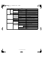
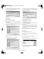
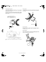
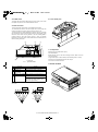
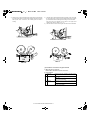
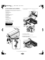
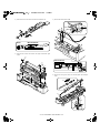
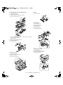
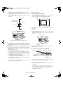
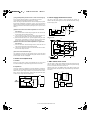
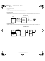
1
CODE : 00ZAL1551/A1E
DIGITAL COPIER
(AL-1551)
MODEL
AL-1340
AL-1451
AL-1551
CONTENTS
[ 1 ] GENERAL . . . . . . . . . . . . . . . . . . . . . . . . . . . . . . . . . . . . . . . . 1 - 1
[ 2 ] SPECIFICATIONS . . . . . . . . . . . . . . . . . . . . . . . . . . . . . . . . . . 2 - 1
[ 3 ] CONSUMABLE PARTS . . . . . . . . . . . . . . . . . . . . . . . . . . . . . . 3 - 1
[ 4 ] EXTERNAL VIEWS AND INTERNAL STRUCTURES . . . . . . . 4 - 1
[ 5 ] UNPACKING AND INSTALLATION. . . . . . . . . . . . . . . . . . . . . . 5 - 1
[ 6 ] COPY PROCESS . . . . . . . . . . . . . . . . . . . . . . . . . . . . . . . . . . . 6 - 1
[ 7 ] OPERATIONAL DESCRIPTIONS. . . . . . . . . . . . . . . . . . . . . . . 7 - 1
[ 8 ] DISASSEMBLY AND ASSEMBLY . . . . . . . . . . . . . . . . . . . . . . 8 - 1
[ 9 ] ADJUSTMENTS . . . . . . . . . . . . . . . . . . . . . . . . . . . . . . . . . . . . 9 - 1
[10] SIMULATION,TROUBLE CODES . . . . . . . . . . . . . . . . . . . . . 10 - 1
[11] USER PROGRAMS . . . . . . . . . . . . . . . . . . . . . . . . . . . . . . . . 11 - 1
[12] ELECTRICAL SECTION . . . . . . . . . . . . . . . . . . . . . . . . . . . . 12 - 1
[13] CIRCUIT DIAGRAM . . . . . . . . . . . . . . . . . . . . . . . . . . . . . . . . 13 - 1
Parts marked with “ “ are important for maintaining the safety of the machine.
Be sure to replace these parts with specified ones for maintaining the safety and performance of the machine.
SHARP CORPORATION
This document has been published to be used for
after sales service only.
The contents are subject to change without notice.
! CAUTION
This product is a class 1 laser product that complies with 21CFR 1040.10 and 1040.11 of the CDRH
standard and IEC825. This means that this machine does not produce hazardous laser radiation. The use
of controls, adjustments or performance of procedures other than those specified herein may result in
hazardous radiation exposure.
This laser radiation is not a danger to the skin, but when an exact focusing of the laser beam is achieved
on the eye’s retina, there is the danger of spot damage to the retina.
The following cautions must be observed to avoid exposure of the laser beam to your eyes at the time of
servicing.
1) When a problem in the laser optical unit has occurred, the whole optical unit must be exchanged as a
unit, not as individual parts.
2) Do not look into the machine with the main switch turned on after removing the developer unit, toner
cartridge, and drum cartridge.
3) Do not look into the laser beam exposure slit of the laser optical unit with the connector connected
when removing and installing the optical system.
4) The middle frame contains the safety interlock switch.
Do not defeat the safety interlock by inserting wedges or other items into the switch slot.
CAUTION
INVISIBLE LASER RADIATION,
WHEN OPEN AND INTERLOCKS DEFEATED.
AVOID EXPOSURE TO BEAM.
VORSICHT
UNSICHTBARE LASERSTRAHLUNG,
WENN ABDECKUNG GEÖFFNET UND
SICHERHEITSVERRIEGELUNG ÜBERBRÜCKT.
NICHT DEM STRAHL AUSSETZEN.
LASER WAVE – LENGTH : 780 ~ 795
Pulse times : 0.481ms/6mm
Out put power : 0.20 ± 0.03mW
VARO !
AVATTAESSA JA SUOJALUKITUS
OHITETTAESSA OLET ALTTIINA
NÄKYMÄTTÖMÄLLE LASERSÄTEILYLLE ÄLÄ
KATSO SÄTEESEEN.
ADVARSEL
USYNLIG LASERSTRÅLNING VED ÅBNING, NÅR
SIKKERHEDSBRYDERE ER UDE AF
FUNKTION. UNDGÅ UDSAETTELSE FOR
STRÅLNING.
VARNING !
OSYNLIG LASERSTRÅLNING NÄR DENNA DEL
ÄR ÖPPNAD OCH SPÄRREN ÄR URKOPPLAD.
BETRAKTA EJ STRÅLEN. – STRÅLEN ÄR
FARLIG.
" At the production line, the output power
of the scanner unit is adjusted to 0.57
MILLI-WATT PLUS 20 PCTS and is
maintained constant by the operation of
the Automatic Power Control (APC).
Even if the APC circuit fails in operation
for some reason, the maximum output
power will only be 15 MILLI-WATT 0.1
MICRO-SEC. Giving and accessible
emission level of 42 MICRO-WATT
which is still-less than the limit of
CLASS-1 laser product.
Caution
This product contains a low power laser
device. To ensure continued safety do not
remove any cover or attempt to gain access
to the inside of the product. Refer all
servicing to qualified personnel.
VAROITUS! LAITTEEN KÄYTTÄMINEN MUULLA
KUIN TÄSSÄ KÄYTTÖOHJEESSA MAINITULLA
TAVALLA SAATTAA ALTISTAA KÄYTTÄJÄN
TURVALLISUUSLUOKAN 1 YLITTÄVÄLLE
NÄKYMÄTTÖMÄLLE LASERSÄTEILYLLE.
VARNING - OM APPARATEN ANVÄNDS PÅ ANNAT
SÄTT ÄN I DENNA BRUKSANVISNING
SPECIFICERATS, KAN ANVÄNDAREN UTSÄTTAS
FÖR OSYNLIG LASERSTRÅLNING, SOM
ÖVERSKRIDER GRÄNSEN FÖR LASERKLASS 1.
The foregoing is applicable only to the 220V
model, 230V model and 240V model.
LUOKAN 1 LASERLAITE
KLASS 1 LASER APPARAT
CONTENTS
[1]
GENERAL
1. Major functions. . . . . . . . . . . . . . . . . . . . . . . . . . . . . . . . . . . 1-1
[2]
SPECIFICATIONS
[8]
DISASSEMBLY AND ASSEMBLY
1. High voltage section . . . . . . . . . . . . . . . . . . . . . . . . . . . . . . .8-1
2. Operation panel section . . . . . . . . . . . . . . . . . . . . . . . . . . . .8-2
1. Basic Specifications . . . . . . . . . . . . . . . . . . . . . . . . . . . . . . . 2-1
3. Optical section . . . . . . . . . . . . . . . . . . . . . . . . . . . . . . . . . . .8-3
2. Operation specifications. . . . . . . . . . . . . . . . . . . . . . . . . . . . 2-1
4. Fusing section. . . . . . . . . . . . . . . . . . . . . . . . . . . . . . . . . . . .8-4
3. Copy performance . . . . . . . . . . . . . . . . . . . . . . . . . . . . . . . . 2-3
5. Tray paper feed/transport section . . . . . . . . . . . . . . . . . . . . .8-7
4. Printer specifications . . . . . . . . . . . . . . . . . . . . . . . . . . . . . . 2-4
6. Manual paper feed section . . . . . . . . . . . . . . . . . . . . . . . . .8-11
5. SPF . . . . . . . . . . . . . . . . . . . . . . . . . . . . . . . . . . . . . . . . . . . 2-4
7. Rear frame section . . . . . . . . . . . . . . . . . . . . . . . . . . . . . . .8-15
6. RSPF . . . . . . . . . . . . . . . . . . . . . . . . . . . . . . . . . . . . . . . . . . 2-4
8. Power section . . . . . . . . . . . . . . . . . . . . . . . . . . . . . . . . . . .8-16
9. SPF section (SPF model only) . . . . . . . . . . . . . . . . . . . . . .8-16
[3]
CONSUMABLE PARTS
1. Supply system table . . . . . . . . . . . . . . . . . . . . . . . . . . . . . . . 3-1
2. Environmental . . . . . . . . . . . . . . . . . . . . . . . . . . . . . . . . . . . 3-1
3. Production control number(lot No.) identification . . . . . . . . . 3-2
10. 2nd cassette section . . . . . . . . . . . . . . . . . . . . . . . . . . . . . .8-19
11. Duplex motor section (RSPF model only). . . . . . . . . . . . . .8-21
12. Reverse roller section (RSPF model only) . . . . . . . . . . . . .8-21
13. RSPF section (RSPF model only) . . . . . . . . . . . . . . . . . . .8-21
[4]
EXTERNAL VIEWS AND INTERNAL STRUCTURES
1. Appearance . . . . . . . . . . . . . . . . . . . . . . . . . . . . . . . . . . . . . 4-1
2. Internal . . . . . . . . . . . . . . . . . . . . . . . . . . . . . . . . . . . . . . . . . 4-1
3. Operation panel . . . . . . . . . . . . . . . . . . . . . . . . . . . . . . . . . . 4-2
4. Motors and solenoids. . . . . . . . . . . . . . . . . . . . . . . . . . . . . . 4-3
5. Sensors and switches . . . . . . . . . . . . . . . . . . . . . . . . . . . . . 4-4
6. PWB unit . . . . . . . . . . . . . . . . . . . . . . . . . . . . . . . . . . . . . . . 4-5
7. Cross sectional view . . . . . . . . . . . . . . . . . . . . . . . . . . . . . . 4-6
[9] ADJUSTMENTS
1. Optical section . . . . . . . . . . . . . . . . . . . . . . . . . . . . . . . . . . .9-1
2. Copy density adjustment . . . . . . . . . . . . . . . . . . . . . . . . . . .9-8
3. High voltage adjustment . . . . . . . . . . . . . . . . . . . . . . . . . . . .9-9
4. Duplex adjustment . . . . . . . . . . . . . . . . . . . . . . . . . . . . . . . .9-9
[10] SIMULATION, TROUBLE CODES
1. Entering the simulation mode . . . . . . . . . . . . . . . . . . . . . . .10-1
2. List of simulations . . . . . . . . . . . . . . . . . . . . . . . . . . . . . . . .10-2
[5]
UNPACKING AND INSTALLATION
1.
Copier installation . . . . . . . . . . . . . . . . . . . . . . . . . . . . . . . . 5-1
2. Cautions on handling . . . . . . . . . . . . . . . . . . . . . . . . . . . . . . 5-1
3. Checking packed components and accessories . . . . . . . . . 5-2
4. Trouble codes . . . . . . . . . . . . . . . . . . . . . . . . . . . . . . . . . .10-14
[11] USER PROGRAM
4. Unpacking . . . . . . . . . . . . . . . . . . . . . . . . . . . . . . . . . . . . . . 5-2
1. Functions which can be set with the user program. . . . . . .11-1
5. Removing protective packing materials . . . . . . . . . . . . . . . . 5-2
2. Change the setting.. . . . . . . . . . . . . . . . . . . . . . . . . . . . . . .11-1
6. Installing the TD cartridge . . . . . . . . . . . . . . . . . . . . . . . . . . 5-2
[6]
3. Contents of simulations (new or revised simulations only) .10-3
[12] ELECTRICAL SECTION
7. Loading copy paper . . . . . . . . . . . . . . . . . . . . . . . . . . . . . . . 5-3
1. Block diagram . . . . . . . . . . . . . . . . . . . . . . . . . . . . . . . . . . .12-1
8. Power to copier . . . . . . . . . . . . . . . . . . . . . . . . . . . . . . . . . . 5-4
2. Circuit descriptions . . . . . . . . . . . . . . . . . . . . . . . . . . . . . . .12-3
9. Installing the printer driver . . . . . . . . . . . . . . . . . . . . . . . . . . 5-4
3. Reset circuit . . . . . . . . . . . . . . . . . . . . . . . . . . . . . . . . . . .12-10
10. Parallel interface. . . . . . . . . . . . . . . . . . . . . . . . . . . . . . . . . . 5-6
4. Heater lamp control circuit . . . . . . . . . . . . . . . . . . . . . . . .12-11
COPY PROCESS
5. Driver circuit (Solenoid) . . . . . . . . . . . . . . . . . . . . . . . . . .12-12
1. Functional diagram . . . . . . . . . . . . . . . . . . . . . . . . . . . . . . . 6-1
6. Toner supply motor drive circuit . . . . . . . . . . . . . . . . . . . .12-12
2. Outline of print process . . . . . . . . . . . . . . . . . . . . . . . . . . . . 6-2
7. Main motor drive circuit. . . . . . . . . . . . . . . . . . . . . . . . . . .12-12
3. Actual print process . . . . . . . . . . . . . . . . . . . . . . . . . . . . . . . 6-2
8. Mirror motor circuit . . . . . . . . . . . . . . . . . . . . . . . . . . . . . .12-13
9. Duplex motor circuit . . . . . . . . . . . . . . . . . . . . . . . . . . . . .12-13
[7]
OPERATIONAL DESCRIPTIONS
1. Outline of operation . . . . . . . . . . . . . . . . . . . . . . . . . . . . . . . 7-1
2. Scanner section . . . . . . . . . . . . . . . . . . . . . . . . . . . . . . . . . . 7-2
3. Laser unit . . . . . . . . . . . . . . . . . . . . . . . . . . . . . . . . . . . . . . . 7-3
4. Fuser section . . . . . . . . . . . . . . . . . . . . . . . . . . . . . . . . . . . . 7-3
5. Paper feed section and paper transport section . . . . . . . . . 7-5
6. Process unit new drum detection mechanism . . . . . . . . . . . 7-8
7. SPF section . . . . . . . . . . . . . . . . . . . . . . . . . . . . . . . . . . . . . 7-8
8. D-D (Duplex to Duplex) mode paper/
document transport (Duplex model). . . . . . . . . . . . . . . . . . . 7-9
10. Power circuit block diagram . . . . . . . . . . . . . . . . . . . . . . .12-14
11. CL invertor PWB (circuit) . . . . . . . . . . . . . . . . . . . . . . . . .12-17
12. CCD PWB operational description . . . . . . . . . . . . . . . . . .12-17
13. Operation section . . . . . . . . . . . . . . . . . . . . . . . . . . . . . . .12-18
[13] CIRCUIT DIAGRAM . . . . . . . . . . . . . . . . . . . . . . . . . . . . .13-1
!
[1] GENERAL
1. Major functions
Configurations
Item
CPM
SB/MB
2 Tray
SPF
R-SPF
FAX
GDI with
USB
Model
AL-1340
13CPM
SB
AL-1451
14CPM
SB
AL-1551
15CPM
MB
GDI
without
USB
PCL with
USB
Descriptions of items
CPM:
SB/MB:
2 tray:
SPF:
R-SPF:
FAX:
GDI with USB:
GDI without USB:
PCL with USB:
SOPM:
Duplex:
Copy speed (Copies Per Minute)
SB = Manual feed single bypass, MB = Manual feed multi bypass
Second cassette unit.
Original feed unit
Duplex original feed unit
FAX function.
GDI printer function with USB.
GDI printer function without USB.
PCL printer function with USB.
Scan Once Print Many function (Many copies are made by one scan.)
Auto duplex copy function
Descriptions of table
: Standard provision
: No function or no option available
Opt: Option
AL-1451
AL-1340
AL-1551
AL-1551 GENERAL 1-1
SOPM
Duplex
!
"#$%
[2] SPECIFICATIONS
1. Basic Specifications
Item
Type
Desktop
Copy system
Dry, electrostatic
Segment (class)
Digital personal copier
Copier dimensions
Weight
(Approximately)
AL-1340
20.4"(W)X17.5"(D)X11.5"(H) (518mm(W)X445mm(D)X293mm(H))
AL-1451
20.4"(W)X18.8"(D)X15.0"(H) (518mm(W)X477mm(D)X379mm(H))
AL-1551
20.4"(W)X18.8"(D)X18.3"(H) (518mm(W)X477mm(D)X464mm(H))
AL-1340
39.7lbs.(18Kg)
AL-1451
47.4lbs.(21.5Kg)
AL-1551
54.3lbs.(24.6Kg)
TD and drum cartridges included
2. Operation specifications
Section, item
Paper feed
section
Paper feed
system
AB system
Tray paper feed
section
Multi bypass paper
feed section
Single bypass paper
feed section
Inch system Tray paper feed
section
Multi bypass paper
feed section
Single bypass paper
feed section
Paper exit section
Originals
Details
AL-1340 / 1451
1 tray (250 sheet) + single bypass
AL-1551
2 tray (500 sheet) + multi bypass (50 sheet)
Paper size
A4, B5, A5 (Landscape)
Paper weight
56 - 80g/m (15 - 21 lbs.)
Paper feed capacity
250 sheets
Kinds
Standard paper, specified paper, recycled paper
Remark
User adjustment of paper guide available
Paper size
A4, B5, A5, B6, A6 (Landscape)
Paper weight
52 - 130g/m (14 - 34.5 lbs.)
Paper feed capacity
50 sheets
Kinds
Standard paper, specified paper, recycled paper, OHP,
Label, Postal card
Remark
User adjustment of paper guide available
Paper size
A4, B5, A5, B6, A6 (Landscape)
Paper weight
52 - 130g/m (14 - 34.5 lbs.)
Paper feed capacity
1 sheet
Kinds
Standard paper, specified paper, recycled paper, OHP,
Label, Postal card
Remark
User adjustment of paper guide available
Paper size
8-1/2" x 14", 8-1/2 x 11", 8-1/2" x 5-1/2" (Landscape)
Paper weight
15 - 21 lbs.
Paper feed capacity
250 sheets
Kinds
Standard paper, specified paper, recycled paper
Remark
User adjustment of paper guide available
Paper size
8-1/2" x 14", 8-1/2 x 11", 8-1/2" x 5-1/2", 3-1/2" x 5-1/2"
(Landscape)
Paper weight
14 - 34.5 lbs.
Paper feed capacity
50 sheets
Kinds
Standard paper, specified paper, recycled paper, OHP,
Label, Postal card
Remark
User adjustment of paper guide available
Paper size
8-1/2" x 14", 8-1/2 x 11", 8-1/2" x 5-1/2" (Landscape)
Paper weight
14 - 34.5 lbs.
Paper feed capacity
1 sheet
Kinds
Standard paper, specified paper, recycled paper, OHP,
Label, Postal card
Remark
User adjustment of paper guide available
Exit way
Face down
Capacity of output tray
100 sheets
Original set
Center Registration (left edge)
Max. original size
B4 (10" x 14")
Original kinds
sheet, book
Original size detection
None
AL-1551 SPECIFICATIONS 2-1
!
"#$%
Section, item
Optical section
Scanning
section
Details
Scanning system
CCD sensor scanning by lighting lamp scanner
CCD sensor
Resolution
400 dpi
Lighting lamp
Type
Xenon lamp
Voltage
1.5kV
Power consumption
11 ± 3W
Gradation
Writing
section
Image forming
Fusing section
Electrical section
256 gradations/8bit
Writing system
Writing to OPC drum by the semiconductor laser
Laser unit
Resolution
600 dpi
Photoconductor
type
OPC (30ø)
Life
18k
Charger
Charging system
Saw -tooth charging with a grid, / (-) scorotron discharge
Transfer system
(+) DC corotron system
Separation system
(-) DC corotron system
Developing
Developing system
Dry, 2-component magnetic brush development system
Cleaning
Cleaning system
Counter blade system (Counter to rotation)
Fusing system
Heat roller system
Upper heat roller
type
Teflon roller
Lower heat roller
type
Silicon rubber roller
Heater lamp
type
Halogen lamp
Voltage
100V
Power consumption
800W
Power source
Power consumption
Voltage
100V, 110V, 120/127V, 230V, 240V
Frequency
Common use for 50 and 60Hz
Max.
Average
(during copying)
1000W
AL-1340
260Wh/H *1)
AL-1451
280Wh/H *1)
AL-1551
310Wh/H *1)
Average (stand-by)
70Wh/H *1)
Pre-heat mode
40Wh/H *1)
Auto power shut-off mode
20Wh/H *1)
*1) May fluctuate due to environmental conditions and the input voltage.
AL-1551 SPECIFICATIONS 2-2
& !
"#$%
3. Copy performance
Section, item
Copy magnification
Details
AL-1340
AL-1451
Fixed
magnification
ratios
3 Reduction + 2 Enlargement
(AB system : 50, 70, 81, 100, 141, 200%)
(Inch system : 50, 64, 78, 129, 100, 200%)
Zooming
magnification
ratios
50 - 200%
(151 steps in 1% increments)
Manual steps
(manual, photo)
AL-1551
5 steps
Copy speed
First copy time Tray paper feed
Manual paper feed
AB system
A4
(Landscape)
Copy speed
(CPM)
AB system
B5
(Landscape)
Copy speed
(CPM)
Inch system
8-1/2" x 14"
(Landscape)
Copy speed
(CPM)
Inch system
8-1/2" x 11"
(Landscape)
Copy speed
(CPM)
Single : 10.0 sec. / Multi : 8.0sec
(Pre-heat mode:16 sec. or below / Auto power-shut-off mode : 23 sec.
or below)
Same size
13
14
15
Enlargement
13
14
15
Reduction
13
14
15
Same size
13
14
15
Enlargement
13
14
15
Reduction
13
14
15
Same size
13
14
15
Enlargement
13
14
15
Reduction
13
14
15
Same size
13
14
15
Enlargement
13
14
15
Reduction
13
14
15
Max. continuous copy quantity
Void
9.6 sec. (Pre-heat mode:16 sec. or below / Auto power-shut-off mode :
23 sec. or below)
99
Void area
leading edge
1 - 4mm
Trailing edge
4mm or less
Side edge void area 3mm or less/per side
Image loss
leading edge
same size: 3.0mm or less / Enlarge (200%): 1.5mm or less / Reduction
(50%): 6.0mm or less
Trailing edge
same size: 3.0mm or less / Enlarge (200%): 1.5mm or less / Reduction
(50%): 6.0mm or less
Side edge void area same size: 3.0mm or less / Enlarge (200%): 1.5mm or less / Reduction
(50%): 6.0mm or less
Warm-up time
0 sec.
Power save mode reset time
0 sec.
Paper jam recovery time
0 sec.
AL-1551 SPECIFICATIONS 2-3
' !
"#$%
4. Printer specifications
Resolution
Page description language
Page onentation
First print time
Print speed(multiple pages)
Interface port
*
600 or 300 can be selected.
SHARP GDI
Portrait or Landscape
Approx. 9.6 seconds*
Max.12 pages per minute(letter or A4)
Bi-directional parallel interface(IEEE 1284 compliant)
First print time may differ depending on operating conditions, such as power-supply voltage and room temperature.
Also the time may differ depending on data quantity to be printed and applications.
5. SPF
Original capacity
Original size
Original replacement speed
Original placement
Original weight
Mixed feeding(Paper size)
Original which cannot
30 sheets (52 to 90g/m)(14 to 23.9 lbs.)
B4 to A5/10" x 14" to 5-1/2" x 8-1/2"
12CPM(A4/8-1/2" x 11"Landscape)(14CPM model)
Face up
52 to 90g/m(14 - 23.9lbs.)
Performance Degraded
Thermal papers, originals with punch holes for files, be used folded paper, transparent originals such as OHP films,
stapled or clip used originals with cover up liquid used, Originals with tape sealed, originals with high level frictional
coefficient such as photos or catalogs.
6. RSPF
Original capacity
Original size
Original replacement speed
Job speed(Tray1,Landscape)
Single copy
Multi copy
Original placement
Original weight
Mixed feeding(Paper size)
Original which cannot
30 sheets (52 to 90g/m)(14 to 23.9 lbs.)
B4 to A5/10" x 14" to 5-1/2" x 8-1/2"
12CPM(A4/8-1/2" x 11"Landscape)(15CPM model)
S to S
12CPM
S to D
5.6CPM
D to S
5.5CPM
D to D
5.2CPM
S to S
15CPM
D to S
15CPM
Face up
52 to 90g/m(14 - 23.9lbs.)
Performance Degraded
Thermal papers, originals with punch holes for files, be used folded paper, transparent
originals such as OHP films, stapled or clip used originals with cover up liquid used,
Originals with tape sealed, originals with high level frictional coefficient such as photos or
catalogs.
AL-1551 SPECIFICATIONS 2-4
!
#$!
%&'()
[3] CONSUMABLE PARTS
1. Supply system table
Common to all destinations
No.
Name
Content
Life
Product name
Package
1
Develop cartridge (Black) x 1
(Except Europe)
Toner/developer cartridge x 1
(Toner: Net weight 220g)(Developer: Net weight 190g)
6K
(5% document)
AL-100TD
5
2
Develop cartridge (Black) x 1
(Except Europe)
Toner/developer cartridge x 1
(Toner: Net weight 124g)(Developer: Net weight 190g)
4K
(5% document)
AL-110TD
5
3
Develop cartridge (Black) x 1
(Europe)
Toner/developer cartridge x 1
(Toner: Net weight 124g)(Developer: Net weight 190g)
4K
(5% document)
AL-110DC
5
4
Drum cartirdge
Drum cartridge
18K
AL-100DR
5
2. Environmental
The environmental conditions for assuring the copy quality and the machine operations are as follows:
(1) Normal operating condition
(4) Supply storage condition
Temperature:20 - 25°C
Humidity:65 ± 5%RH
Humidity (RH)
90%
(2) Acceptable operating condition
Humidity (RH)
85%
60%
20%
20%
–5˚C
10˚C
30˚C
35˚C
30˚C
40˚C
(3) Optical condition
Humidity (RH)
90%
60%
15%
–25˚C
AL-1551 CONSUMABLE PARTS 3-1
45˚C
* !
#$!
%&'()
3. Production control number(lot No.)
identification
<Developing cartridge>
Production month
Production day
Destination code
(Dealer, distributor, OEM, etc.)
Production place
(SOCC: Fixed to B.)
End digit of year
Version No.
Production control
label attachment position
*
Destination
Division
EX Destination
Option Destination
No.
A same pack
G
B same pack
H
A
P
B
Q
<Drum cartridge>
The label on the drum cartridge shows the date of production.
(SOCC production)
Production month
Production day
Destination code
Production control
label attachment position(*1)
(Dealer, distributor, OEM, etc.)
Production place
(SOCC: Fixed to B.)
End digit of year
Version No.
*1 The production control label is not attached to the cartridge of a
China product.
<JAPAN production>
Ver.A
9
1
1
0001
X
Production month
(1 - 9 = Jan. - Sep. 0 = Oct. X = Nov. Y = Dec.)
Serial number of month
Fixed to 1.
Pack division
(See table below)
End digit of year
Version No.
Division
No.
Ex production
1
Option
2
Same pack
3
AL-1551 CONSUMABLE PARTS 3-2
!"
#$%&'
[4] EXTERNAL VIEWS AND INTERNAL STRUCTURES
1. Appearance
Original cover
10
11
SPF
17
18
9
19
1
12
RSPF
21
2
8
20
18
3
6
1
4
7
10
13
16
19
19
4
7
16
20
15
5
14
Original cover
Bypass tray guides
Paper tray
Handle
Paper output tray extension
Power cord socket
Document feeder tray
2
5
8
11
14
17
20
Side cover
Side cover open button
Operation panel
GDI printer interface
Handle
SPF exit area *1
Feeding roller cover
3
6
9
12
15
18
21
Bypass tray
Front cover
Original table
Paper output tray
Power switch
Original guides
RSPF exit area *2
*1 SPF only *2 RSPF only
2. Internal
1
3
2
4
7
5
1
4
7
TD cartridge lock release button
Drum cartridge handle
Transfer charger
2
5
TD cartridge
Fusing unit release lever
6
3
6
Drum cartridge
Charger cleaner
AL-1551 EXTERNAL VIEWS AND INTERNAL STRUCTURES 4-1
( !"
#$%&'
3. Operation panel
1
2
3
4
(AL-1551)
1
13
5
6
7
14
Duplex Mode select key and indicator
Light and dark keys and exposure indicators
9
15
10
16
11
12
17
18
2
Exposure mode selector key and indicators
4
Use to sequentially select the exposure modes: AUTO, MANUAL or
PHOTO. Selected mode is shown by a lit indicator.
Alarm indicators
(RSPF only)
3
8
Use to adjust the MANUAL or PHOTO exposure level.
Selected exposure level is shown by a lit indicator.Use to start and
terminate user program setting.
Drum replacement required indicator
Misfeed indicator
TD cartridge replacement required indicator
5
7
SPF indicator
Copy ratio selector key and copy ratio indicators
6
8
SPF misfeed indicator
Zoom indicator
9
Use to sequentially select preset reduction/enlargement copy
ratios.
Selected copy ratio is shown by a lit indicator.
Copy ratio display (%) key
10
Display
11
ON LINE indicator
12
Displays the specified copy quantity, zoom copy ratio, user program
code, and error code.
Power save indicator
13
Lights up when the machine is used as a printer.
Tray select key
14
Lights up when the copier is in a power save mode.
Paper feed location indicators
15
Use to select a paper feed station (paper tray or bypass tray).
Zoom keys
16
Light up to show the selected paper feed station.
Copy quantity keys
Use to select any reduction or enlargement copy ratio from 50% to
200% in 1% increments.
17
Clear key
•Use to select the desired copy quantity (1 to 99).
18
•Press to clear the display, or press during a copy run to terminate
copying.
•Use to make user program entries.
Print key and ready indicator
•Copying is possible when the indicator is on.
•Use to set a user program.
•Press and hold down during standby to display the total number of
copies made to date.
AL-1551 EXTERNAL VIEWS AND INTERNAL STRUCTURES 4-2
) !"
#$%&'
4. Motors and solenoids
3
9
2
10
8
4
1
5
7
6
11
No.
1
Part name
Main motor
Control signal
MM
Function,operation
Drives the copier.
2
Mirror motor
MRMT
Drives the optical mirror base (scanner unit).
3
Toner motor
TM
Supplies toner.
4
Cooling fan motor
VFM
Cools the optical section.
5
Resist roller solenoid
RRS
Resist roller rotation control solenoid
6
Paper feed solenoid
CPFS1
Cassette Paper feed solenoid 1
7
Multi paper feed solenoid
MPFS
Multi manual pages feed solenoid
8
SPF motor
SPFM
Drives the single pass feeder
9
Duplex motor
DMT
Devices the duplex paper transport section
10
Original feed solenoid
SPUS
Original feed solenoid
11
Paper feed solenoid
CPFS2
Cassette Paper feed solenoid 2
AL-1551 EXTERNAL VIEWS AND INTERNAL STRUCTURES 4-3
!"
#$%&'
5. Sensors and switches
1
12
2
10
11
3
4
13
5
9
6
7
14
8
No.
Name
Signal
Type
Transmission sensor
Function
Mirror (scanner unit) home position
detection
Output
1
Mirror home position sensor MHPS
"H" at home position
2
POD sensor
POD
Transmission sensor
Paper exit detection
"H" at paper pass
3
PPD2 sensor
PPD2
Transmission sensor
Paper transport detection 2
"L" at paper pass
4
Cassette detection switch
CED1
Microswitch
Cassette installation detection
"H" at cassette insertion
5
Manual feed detection switch MFD
Transmission sensor
Manual feed paper detection
(single only)
"L" at paper detection
6
PPD1 sensor
PPD1
Transmission sensor
Paper transport detection 1
"L" at paper pass
7
Door switch
DSW
Micro switch
Door open/close detection
(safety switch for 5V)
1 or 0V of 5V at door open
8
Door switch
DSW
Micro switch
Door open/close detection
(safety switch for 24V)
1 or 0V of 24V at door open
9
Drum reset switch
DRST
Micro switch
New drum detection switch
Instantaneously "H" at insertion of new
drum
10
SPF sensor
SPID/
SD SW
Transmission sensor
Paper entry detection
Cover open/close detection
"L" at paper pass
11
SPPD sensor
SPPD
Transmission sensor
Paper transport detection
"L" at paper pass
12
SDOD sensor
SDOD
Transmission sensor
SPF open/close detection Book sensor "L" at paper pass
13
2nd cassette
DSW
Micro switch
2nd cassette door open detection
1 or 0V of 5V at door open
14
PPD3 sensor
PPD3
Transmission sensor
Paper transport detection 3
"L" at paper pass
AL-1551 EXTERNAL VIEWS AND INTERNAL STRUCTURES 4-4
* !"
#$%&'
6. PWB unit
10
2
1
9
5
8
6
4
3
7
No.
Name
Function
1
Exposure lamp invertor PWB
Exposure lamp (Xenon lamp) control
2
Main PWB (MCU)
Copier control
3
Operation PWB
Operation input/display
4
Power PWB
AC power input, DC voltage control, High voltage control
5
CCD sensor PWB
For image scanning
6
LSU motor PWB
For polygon motor drive
7
TCS PWB
For toner sensor control
8
LSU PWB
For laser control
9
Memory PWB 6MB
For memorying data
10
GDI Printer PWB
GDI Printer control
AL-1551 EXTERNAL VIEWS AND INTERNAL STRUCTURES 4-5
+ !"
#$%&'
7. Cross sectional view
19
4
5
16
17
6
3
18
1
2
7
8
9
10
11
12
15
No.
1
14
Part name
Scanner unit
13
Function and operation
Illuminates the original with the copy lamp and passes the reflected light to the lens unit(CCD).
2
Exposure lamp
Exposure lamp (Xenon lamp) Illuminates original
3
Lens unit
Scans the original image with the lens and the CCD.
4
LSU (Laser unit)
Converts the original image signal into laser beams and writes onto the drum.
5
Paper exit roller
Roller for paper exit
6
Main charger
Provides negative charges evenly to the drum surface.
7
Heat roller
Fuses toner on the paper. (Teflon roller)
8
Pressure roller
Fuses toner on the paper. (Silicon rubber roller)
9
Drum
Forms images.
10
Transfer unit
Transfers images onto the drum.
11
Pickup roller
Picks up the manual feed paper. (In multi feed only)
12
Manual paper feed tray
Tray for manual feed paper
13
Manual paper feed roller
Transport the paper from the manual paper feed port.
14
PS roller unit
Takes synchronization between the lead edge and the rear edge of the paper.
15
Paper feed roller
Picks up a sheet of paper from the cassette.
16
Pickup roller
Picks up documents.
17
Separation roller
Separates documents to feed properly.
18
PS roller
Feeds documents to the scanning section.
19
Paper exit roller
Discharges documents.
AL-1551 EXTERNAL VIEWS AND INTERNAL STRUCTURES 4-6
!
#$!
%&'()*
[5] UNPACKING AND INSTALLATION
1. Copier installation
Improper installation may damage the copier. Please note the following
during initial installation and whenever the copier is moved.
2. Cautions on handling
Be careful in handling the copier as follows to maintain the performance
of this copier.
Do not drop the copier, subject it to shock or strike it against any object.
Caution: If the copier is moved from a cool place to a warm place,
condensation may form inside the copier. Operation in this
condition will cause poor copy quality and malfunctions.
Leave the copier at room temperature for at least 2 hours before
use.
Do not install your copier in areas that are:
• damp, humid, or very dusty
Do not expose the drum cartridge to direct sunlight.
Doing so will damage the surface (green portion) of the drum cartridge,
causing poor print quality.
• exposed to direct sunlight
• poorly ventilated
Store spare supplies such as drum cartridges and TD cartridges in a
dark place without removing from the package before use.
If they are exposed to direct sunlight, poor print quality may result.
Do not touch the surface (green portion) of the drum cartridge.
Doing so will damage the surface of the cartridge, causing poor print
quality.
• subject to extreme temperature or humidity changes, e.g., near an air
conditioner or heater.
The copier should be installed near an accessible power outlet for easy
connection.
Be sure to connect the power cord only to a power outlet that meets the
specified voltage and current requirements.
Also make certain the outlet is properly grounded.
Be sure to allow the required space around the machine for servicing
and proper ventilation.
+
4"
(10cm)
8"(20cm)
4"
(10cm)
AL-1551 UNPACKING AND INSTALLATION 5-1
+ !
#$!
%&'()*
3. Checking packed components and
accessories
Open the carton and check if the following components and accessories
are included.
Interface cable
(IBM PC/AT or compatible computer)
Power cord
6. Installing the TD cartridge
The TD cartridge replacement required ( ) indicator will light up when
toner is needed. If copying is continued while the
indicator is lit,
copies will gradually become lighter until the copier stops and the
indicator begins blinking. Replace the old TD cartridge by following the
procedure given below.
Note:
•After the copier stops, it may be possible to make a few more copies by
taking the TD cartridge out of the copier, shaking it horizontally, then
reinstalling it. If copying is not possible after this operation, replace the
TD cartridge.
Operation manual
Printer driver (CD-ROM)
•During long copy run of a dark original, the ready (
) indicator may
blink, the
indicator may light up, and the copier may stop, even
though toner cartridge is not empty. The copier will feed toner up to 2
minutes and then the ready (
) indicator will light up. Press the print
(
) key to restart copying.
TD cartridge
Copier
Drum cartridge
(installed in copier)
1) Ensure that the bypass tray is open and then open the side cover by
pressing the open button on the side cover.
4. Unpacking
Be sure to hold the handles on both sides of the copier to unpack the
copier and carry it to the installation location.
5. Removing protective packing materials
2) Remove the CAUTION tape from the front cover and remove the two
protective pins from the fusing unit by pulling the strings upward one
at a time.
1) Remove pieces of tape and protective cover. Then open the original
cover and remove protective materials (a) and (b).
CAUTION tape
Protective pins
3) Push gently on both sides of the front cover to open the cover.
2) Use a coin (or suitable object) to remove the screw.
Store the screw in the paper tray because it will be used if the copier
has to be moved.
AL-1551 UNPACKING AND INSTALLATION 5-2
, !
#$!
%&'()*
4) Remove the TD cartridge from the bag. Remove the protective paper.
Hold the cartridge on both sides and shake it horizontally four or five
times.
4 or 5 times
7. Loading copy paper
Note: This copier is equipped with two paper trays. Load copy paper into
the two paper trays.
1) Raise the handle of the paper tray and pull the paper tray out until it
stops.
5) Hold the tab of the protective cover and pull the tab to remove the
cover.
6) Gently insert the TD cartridge until it locks in place.
2) Remove the pressure plate lock. Rotate the pressure plate lock in the
direction of the arrow to remove it while pressing down the pressure
plate of the paper tray.
3) Store the pressure plate lock which has been removed in step 2 and
the screw which has been removed when unpacking in the front of
the paper tray. To store the pressure plate lock, rotate the lock to fix it
on the relevant location.
4) Adjust the paper guides on the paper tray to the copy paper width
and length.
Squeeze the lever of paper guide (A) and slide the guide to match
with the width of the paper.
Move paper guide (B) to the appropriate slot as marked on the tray.
Paper guide (B)
7) Close the front cover and then the side cover by pressing the round
projections near the side cover open button. The
indicator will go
out and the ready (
) indicator will light up.
Note: When closing the covers, be sure to close the front cover securely
and then close the side cover. If the covers are closed in the wrong
order, the covers may be damaged.
Paper guide (A)
5) Fan the copy paper and insert it into the tray. Make sure the edges go
under the corner hooks.
Note: Do not load paper above the maximum height line (
).
Exceeding the line will cause a paper misfeed.
6) Gently push the paper tray back into the copier.
Note: After loading copy paper, to cancel the blinking "H" without
restarting copying, press the clear (
) key. The "P" in the display
will go out and the ready (
) indicator will light up.
AL-1551 UNPACKING AND INSTALLATION 5-3
"#
$%&'
8. Power to copier
A. Windows 95/Windows NT 4.0
1) Ensure that the power switch of the copier is in the OFF position.
Insert the attached power cord into the power cord socket at the rear
of the copier.
2) Plug the other end of the power cord into the nearest outlet.
1) Load paper into the paper tray of the printer.
2) Turn on the printer.
3) Turn on your computer and start Windows.
9. Installing the printer driver
4) When using Windows 95 on a personal computer with plug & play,
the "Update Device Driver Wizard" window will appear. Insert the
installation CD-ROM into the CD-ROM drive. Click the Next button
and follow the on-screen instructions. If the "Copying Files" window
appears during this operation, enter R:\ (substitute the letter of your
CD-ROM drive for "R"), click the OK button and follow the on-screen
instructions.
(Description of the printer driver)
The printer driver is the software program which runs the printer. It
converts the data in your file into information that the printer can
understand. It also controls communication between the printer and
computer as the data is printed.
• Before installing the printer driver, be sure to close all other applications
which may be open.
(Checking the hardware and software requirements)
You will need the following hardware and software in order to install the
printer driver.
Computer type
Windows type
Display
Hard disk
free space
IBM PC/AT or compatible computer equipped with a
bi-directional parallel interface and CD-ROM drive
Windows 3.1x, Windows 95, Windows 98,
Windows Me, Windows NT 4.0, Windows 2000
640 x 480 dots (VGA) or better
10 MB or more
Hardware requirements, such as CPU performance rating and amount of
RAM installed, are the same as for your operating system.
• The printer driver included in this product cannot be used under
Windows NT 3.5x, OS/2, pure MS-DOS and other operating systems
which are not described above.
• If you are using some of your computer’s memory as a RAM drive, the
printer driver may not be allocated the correct amount of memory. In
such a case, reduce the size of your RAM disk, or do not use the RAM
disk. Please refer to your MS Windows documentation for further
information.
• If you are using Windows 95 and the "New Hardware Found" window
will appear, select Driver from Disk Provided by Hardware Manufacturer
and then click the OK button. Proceed to step 6.
• If you are using Windows 95 and the screen shown above or the "New
Hardware Found" window does not appear, proceed to step 5.
• If you are using Windows NT 4.0, proceed to step 5.
*
(Installing the printer driver)
The software for your printer is provided on CD-ROM.
Before installing the printer driver, be sure to check the following items.
• Is the printer connected properly to the computer?
Plug & play
This feature is effective if both the computer and peripheral
equipment are equipped with IEEE 1284 compliant parallel interface.
Note: The screen displayed depends on the version of Windows.
• Does the printer have paper?
• Is there another GDI printer driver or Windows Printing System printer
driver already installed? If installed, change the printer port setting.
5) Insert the installation CD-ROM into the CD-ROM drive.
Click the Start button and select Run. When the screen shown below
appears, type R:\SETUP(substitute the letter of your CD-ROM drive
for "R") and click the OK button. Follow the on-screen instructions.
AL-1551 UNPACKING AND INSTALLATION 5-4
"#
$%&'
6) The "Install From Disk" window will appear. Insert the installation CDROM into the CD-ROM drive. Type R:\ (substitute the letter of your
CD-ROM drive for "R") and click the OK button.
Follow the on-screen instructions.
8) Insert the installation CD-ROM into the CD-ROM drive. Click the
Start button and select Run. When the window shown below
appears, type R:\SETUP (substitute the letter of your CD-ROM drive
for "R") and click the OK button.
Follow the on-screen instructions.
B. Windows 98:
1) Load paper into the paper tray of the printer.
2) Turn on the printer.
3) Turn on your computer and start Windows.
C. Windows Me/Windows 2000:
• Before installing the printer driver, be sure to close all other applications
which may be open.
4) When using Windows 98 on a personal computer with plug & play,
the "Add New Hardware Wizard" window will appear. Click the Next
button and follow the on-screen instructions.
• If the "Add New Hardware Wizard" window does not ap-pear, proceed
to step 8.
1) Load paper in the paper tray of the printer.
2) Turn on the printer.
3) Turn on your computer and start Windows.
• If a Plug & Play dialog box appears when you start Windows, click the
Cancel button to close the dialog box.
• Before installing the printer driver, be sure to close all other applications
which may be open.
4) Insert the installation CD-ROM into the CD-ROM drive. Click the
Start button and select Run. Type R:\SETUP (substitute the letter of
your CD-ROM drive for "R") and click the OK button. Follow the onscreen instructions.
• If the "Found New Hardware Wizard" window appears when you start
Windows after installing the printer driver, click the Finish button.
D. Windows 3.1x:
1) Load paper into the paper tray of the printer.
2) Turn on the printer and then start Windows on your computer.
• Before installing the printer driver, be sure to close all other applications
which may be open.
5) Select Search for the best driver for your device and click the Next
button.
6) Insert the installation CD-ROM into the CD-ROM drive.
Select CD-ROM drive and click the Next button.
3) Insert the installation CD-ROM into a CD-ROM drive.
4) Choose File from the Menu bar in Program Manager, and then
choose the Run... command.
5) Type R:\SETUP (substitute the letter of your CD-ROM drive for "R")
in the command line box and then click the OK button..
6) Follow the on-screen instructions.
7) Windows driver file search will find the device “SHARP AL-1000
Series”. Click the Next button and follow the on-screen instructions.
AL-1551 UNPACKING AND INSTALLATION 5-5
( "#
$%&'
E. AL-1000 Series printer driver group
10.Parallel interface
When the printer driver is installed, the SHARP AL-1000 Series printer
driver group will be created. This group allows the following functions to
be executed.
This printer uses a bi-directional parallel interface. Use the sup-plied
interface cable.
Connector
Uninstall AL-1000 Series
The printer driver can be uninstalled. If the driver is uninstalled, printing
cannot be performed on the printer. For proper uninstallation, be sure to
use uninstallation program of the printer driver group.
Readme
The latest information on the printer driver is included in this note. Read
the Readme first.
36-pin DDK 57LE-40360-730B (D29) female connector or equivalent
connector
Cable
Shielded type bi-directional parallel interface For best results, use a
printer interface cable which is IEEE1284 compliant.
Pin configuration
The pin numbers and signal names are listed in the follow-ing table.
18
1
36
19
Advanced Settings
See help for application support and application problems that may occur
when printing. See help for the applicable method of usage.
Status Monitor
The printer state and information on current printing are displayed on the
status monitor window.
DOS Emulation Setup
Pin No.
Signal name
Pin No.
Signal name
1
STB
19
GND (STB RET)
Status Monitor HELP
2
DATA1
20
GND (DATA1 RET)
DOS Emulation HELP
3
DATA2
21
GND (DATA2 RET)
Advanced Settings HELP
4
DATA3
22
GND (DATA3 RET)
• Be sure to read "Readme" found in the printer driver group before
starting to print from application programs.
5
DATA4
23
GND (DATA4 RET)
6
DATA5
24
GND (DATA5 RET)
7
DATA6
25
GND (DATA6 RET)
8
DATA7
26
GND (DATA7 RET)
9
DATA8
27
GND (DATA8 RET)
28
GND
(ACKNLG RET)
10
ACKNLG
11
BUSY
29
GND (BUSY RET)
12
PE (Paper End)
30
GND (PE RET)
13
SLTC
31
INPRM
14
AUTO LF
32
FAULT
15
(NC)
33
(NC)
16
GND (0 V)
34
(NC)
17
FG
35
+5 V
18
+5 V
36
SLTC IN
AL-1551 UNPACKING AND INSTALLATION 5-6
!
"#$%&'
[6] COPY PROCESS
An OPC drum is used for the photoconductor.
(Structure of the OPC drum layers)
OPC layer
(20microns thick)
Pigment layer (0.2
to 0.3 microns thick)
Aluminium drum
1. Functional diagram
Main charger
Laser beam
Cleaning blade
MG roller
Drum
Transfer unit
Resist roller
(Basic operation cycle)
Semiconductor laser
Focus correction lens
Main high voltage unit
Exposure
Charge
Saw tooth
Toner
Drum
Developing
Cleaning
Developer
Cleaning blade
PS roller
Waste toner box
To face
down tray
Paper release
Fusing
Separation
Transfer
Heat roller
Electrode
Transfer charger
Heater lamp
Synchronization
with drum
Manual feed
Cassette
paper feed
Transfer high
voltage unit
Print process
Paper transport route
AL-1551 COPY PROCESS 6-1
( !
"#$%&'
2. Outline of print process
Step-2: Exposure (laser beam, lens)
This printer is a non-impact printer that uses a semiconductor laser and
electrostatic print process. This printer uses an OPC (Organic Photo
Conductor) for its photoconductive material.
First, voltage from the main corona unit charges the drum surface and a
latent image is formed on the drum surface using a laser beam. This
latent image forms a visible image on the drum surface when toner is
applied. The toner image is then transferred onto the print paper by the
transfer corona and fused on the print paper in the fusing section with a
combination of heat and pressure.
Step-1: Charge
Step-2: Exposure
* Latent image is formed on the drum.
Step-3: Developing
Latent image formed on the drum is then changed into visible
image with toner.
Step-4: Transfer
The visible image (toner image) on the drum is transferred onto
the print paper.
Step-5: Cleaning
Residual toner on the drum surface is removed and collected by
the cleaning blade.
Step-6: Optical discharge
Residual charge on the drum surface is removed, by
semiconductor laser beam.
3. Actual print process
A Laser beam is generated from the semiconductor laser and controlled
by the print pattern signal. The laser writes onto the OPC drum surface
through the polygon mirrors and lens. The resistance of the OPC layer
decreases for an area exposed by the laser beam (corresponding to the
print pattern signal). The beam neutralizes the negative charge. An
electrostatic latent image is formed on the drum surface.
Semiconductor laser
Exposure
(semiconductor laser)
OPC layer
Pigment
layer
Aluminum
drum
Drum surface charge
sfter the exposure
Step-1: DC charge
A uniform negative charge is applied over the OPC drum surface by the
main charging unit. Stable potential is maintained by means of the
Scorotron charger.
Positive charges are generated in the aluminum layer.
About
DC5.5KV
( 580V/ 400V)
AL-1551 COPY PROCESS 6-2
Non-image area
Image area
OPC layer
Pigment
layer
Aluminum
layer
) !
"#$%&'
Step-3: Developing (DC bias)
Step-4: Transfer
A bias potential is applied to the MG roller in the two component
magnetic brush developing method, and the toner is charged negative
through friction with the carrier.
Non-image area of the drum surface charged with negative potential
repel the toner, whereas the laser exposed portions where no negative
charges exist, attract the toner. As a result, a visible image appears on
the drum surface.
The visible image on the drum surface is transferred onto the print paper
by applying a positive charge from the transfer corona to the backside of
the print paper.
:Carrier (Magnetized particle)
:Toner (Charge negative by friction)
(N) (S) Permanent magnet
(provided in three locations)
N
S
N
About DC 5.2kV
DC
400V 8V
MG roller
Step-5: Separation
Since the print paper is charged positively by the transfer corona, it is
discharged by the separation corona. The separation corona is
connected to ground.
Step-6: Cleaning
Toner remaining on the drum is removed and collected by the cleaning
blade. It is transported to the waste toner collecting section in the
cleaning unit by the waste toner transport roller.
Toner is attracted over the shadowed area because of the developing
bias.
AL-1551 COPY PROCESS 6-3
* !
"#$%&'
Step-7: Optical discharge (Semiconductor laser)
Start
Before the drum rotation is stopped, the semiconductor laser is radiated
onto the drum to reduce the electrical resistance in the OPC layer and
elimate residual charge, providing a uniform state to the drum surface for
the next page to be printed.
When the electrical resistance is reduced, positive charges on the
aluminum layer are moved and neutralized with negative charges on the
OPC layer.
1) Because the grid potential is at a low level, the drum potential is at
about -400V. (Carrier may not be attracted though the carrier is
pulled towards the drum by the electrostatic force of -400V.
2) Developing bias (-400V) is applied when the photoconductor
potential is switched from LOW to HIGH.
3) Once developing bias (-400V) is applied and the photo conductor
potential rises to HIGH, toner will not be attracted to the drum.
Semiconductor laser
Stop
The reverse sequence takes place.
Retaining developing bias at an abnormal occurrence
Function
The developing bias will be lost if the power supply was removed during
print process. In this event, the drum potential slightly abates and the
carrier makes deposits on the drum because of strong static power. To
prevent this, the machine incorporates a function to retain the developing
bias for a certain period and decrease the voltage gradually against
possible power loss.
Charge by the Scorotron charger
Function
The Scorotron charger functions to maintain uniform surface potential on
the drum at all times, It control the surface potential regardless of the
charge characteristics of the photoconductor.
Basic function
A screen grid is placed between the saw tooth and the photoconductor. A
stable voltage is added to the screen grid to maintain the corona current
on the photoconductor.
As the photoconductor is charged by the saw tooth from the main corona
unit, the surface potential increases. This increases the current flowing
through the screen grid. When the photoconductor potential nears the
grid potential, the current turns to flow to the grid so that the
photoconductor potential can be maintained at a stable level.
Basic function
Normally, the developing bias voltage is retained for a certain time before
the drum comes to a complete stop if the machine should stop before
completing the normal print cycle. The developing bias can be added
before resuming the operation after an abnormal interruption. Therfore,
carrier will not make a deposit on the drum surface.
Process controlling
Function
The print pattern signal is converted into an invisible image by the
semiconductor laser using negative to positive (reversible) developing
method. Therefore, if the developing bias is added before the drum is
charged, toner is attracted onto the drum. If the developing bias is not
added when the drum is charged, the carrier is attracted to the drum
because of the strong electrostatic force of the drum.
To avoid this, the process is controlled by adjusting the drum potential
and the grid potential of the Scorotron charger.
Basic function
Voltage added to the screen grid can be selected, high and low. To make
it easily understood, the figure below shows voltage transition at the
developer unit.
START
STOP
0
Print potentioal
Toner attract
potential
Developing bias
2)
3)
1)
Low
4)
Drum potential
High
Time
AL-1551 COPY PROCESS 6-4
"#
$%&'
[7] OPERATIONAL DESCRIPTIONS
1. Outline of operation
The outline of operation is described referring to the basic configuration.
(Basic configuration)
Scanner section
PC
CCD
Operation
section
MCU (Main control/image process section)
PCL control
PCL I / F
LSU (Laser unit)
Laser diode, Polygon mirror lens
Laser beam
Paper exit
Fusing section
Process section
Printer section
Paper transport section
Cassette paper
feed section
Manual paper
feed section
(Outline of copy operation)
Setting conditions
1) Set copy conditions such as the copy quantity and the copy density with the operation section, and press the COPY button. The information on copy
conditions is sent to the MCU.
Image scanning
2) When the COPY button is pressed, the scanner section starts scanning of images.
The light from the copy lamp is reflected by the document and passed through the lens to the CCD.
Photo signal/Electric signal conversion
3) The image is converted into electrical signals by the CCD circuit and passed to the MCU.
Image process
4) The document image signal sent from the CCD circuit is processed under the revised conditions and sent to the LSU (laser unit) as print data.
Electric signal/Photo signal (laser beam) conversion
5) The LSU emits laser beams according to the print data.
(Electrical signals are converted into photo signals.)
6) The laser beams are radiated through the polygon mirror and various lenses to the OPC drum.
Printing
7) Electrostatic latent images are formed on the OPC drum according to the laser beams, and the latent images are developed to be visible
images(toner images).
8) Meanwhile the paper is fed to the image transfer section in synchronization with the image lead edge.
9) After the transfer of toner images onto the paper, the toner images are fused to the paper by the fusing section. The copied paper is discharged
onto the exit tray.
AL-1551 OPERATIONAL DESCRIPTIONS 7-1
( "#
$%&'
2. Scanner section
B. Basic structure of scanner section
A. How to scan documents
(11)
The scanner has sensors that are arranged in a line. These sensors
scan a certain area of a document at a time and deliver outputs
sequentially. When the line is finished, the next line is scanned, and this
procedure is repeated.
The figure below shows the case where the latter two sections of an
image which are scanned are shown with solid lines and the former two
sections which are being transmitted are shown with dotted lines.
The direction of this line is called "main scanning direction," and the
scanning direction "sub scanning direction."
In the figure below, one line is divided into 4 sections. Actually, however,
one line is divided into thousands of sections. For scanning, the light
receiving element called CCD is used.
The basic resolution indicates the scanner capacity. The basic resolution
is expressed in dpi (dot/inch) which shows the number of light emitting
elements per inch on the document.
The basic resolution of this machine is 400dpi.
In the sub scanning direction, at the same time, the motor that drives the
optical system is controlled to scan the image at the basic resolution.
Sub scanning direction
Sensor scanning area
Main
scanning
direction
(1)
(4)
(5)
(7)
Copy lamp (Xenon lamp)
3
5
7
9
11
No. 1 mirror
No. 3 mirror
No. 2/3 mirror unit
CCD
MHPS
(Mirror home position sensor)
2
3
4
5
Image data sent to the ICU PWB
3
2
(8)
(6)
(9) (10)
2
Reflector
(light conversion plate)
4 No. 2 mirror
6 Lens
8 Copy lamp unit
10 Mirror motor
The scanner unit performs scanning in the digital optical system.
The light from the light source (Xenon lamp) is reflected by a document
and passed through three mirrors and reduction lenses to the CCD
element (image sensor) where images are formed. This system is known
as the reduction image sensor system. Photo energy on the CCD
element is converted into electrical signals (analog signals). (Photoelectric conversion). The output signals (analog signals) are converted
into digital signals (A/D conversion) and passed to the MCU (main
control/image process section). The resolution at that time is 400dpi.
The mirror unit in the scanner section is driven by the mirror motor.
The MHPS is provided to detect the home position of the copy lamp unit.
1
4
(3)
1
Original
5
(2)
1
To MCU PWB
AL-1551 OPERATIONAL DESCRIPTIONS 7-2
) "#
$%&'
3. Laser unit
B. Laser beam path
The image data sent from the MCU (image process circuit) is sent to the
LSU (laser unit), where it is converted into laser beams.
A. Basic structure
The LSU unit is the writing section of the digital optical system.
The semiconductor laser is used as the light source, and images are
formed on the OPC drum by the polygon mirror and fθ lens, etc.
The laser beams are passed through the collimator lens, the cylindrical
lens, the polygon mirror, the fθ lens, and the mirror to form images on the
OPC drum in the main scanning direction. The laser emitting PWB is
provided with the APC (auto power control) in order to eliminate
fluctuations in the laser power. The BF PWB works for measurement of
the laser writing start point.
(3)
(2)
(1)
(4)
C. Composition
Effective scanning width:216mm (max.)
Resolution:600dpi
Beam diameter: 75um in the main scanning direction, 80um in the sub
scanning direction
Image surface power:0.20 ±0.03mW (Laser wavelength 780 - 795nm)
Polygon motor section:Brushless motor 20.787rpm
No. of mirror surfaces:6 surfaces
(5)
: Laser beam
path for BF PWB
4. Fuser section
No
Component
Function
(1) Semiconductor laser
Generates laser beams.
(2) Collimator lens
Converges laser beams in parallel.
(3) Polygon mirror,
polygon motor
Reflects laser beams at a constant rpm.
(4) BD (Mirror, lens, PWB) Detects start timing of laser scanning.
(5) fθ lens
Converges laser beams at a spot on the
drum.
Makes the laser scanning speeds at both
ends of the drum same as each other.
(Refer to the figure below.)
Makes the laser scanning speeds at both ends of the drum same as
each other.
a≠b≠c
a
b
d=e=f
c
d
e
f
f θ LENS
AL-1551 OPERATIONAL DESCRIPTIONS 7-3
* "#
$%&'
A. General description
(3) Thermal control
General block diagram (cross section)
1) The heater lamp, thermistor, main PWB, DC power supply PWB, and
triac within the power supply unit are used to control the temperature
in the fuser unit.
To prevent against abnormally high temperature in the fuser unit, a
thermal breaker and thermal fuse are used for safety purposes.
Thermal fuse
Separator pawl
PPD2
Heated by the heater
lamp.(950W)
Thermistor
Pressure roller
Saftey device
(Thermal breaker, thermal
fuse)
The surface temperature
of the upper heat roller is
sensed by the thermistor.
Heat roller
Triac (in the
power supply unit)
Paper guide
Level of the thermistor is
controlled by the main PWB.
With th e signal from the
main PWB, the triac is
controlled on and o ff.
(power supply PWB )
Top view
Heat roller
Thermistor
Thermal fuse
Heater lamp
Separator pawl
(1) Heat roller
A teflon roller is used for the heat roller and a silicone rubber roller is
used for the lower heat roller for better toner fusing performance and
paper separation.
2) The surface temperature of the upper heat roller is set to 165 190°C. The surface temperature during the power save mode is set
to 100°C.
3) The self-check function comes active when one of the following
malfunctions occurs, and an "H" is displayed on the multicopy
window.
a. When the heat roller surface temperature rises above 240°C.
b. When the heat roller surface temperature drops below 100°C during
the copy cycle.
c. Open thermistor
d. Open thermal fuse
e. When the heat roller temperature does not reach 190°C within 27
second after supplying the power.
(2) Separator pawl
(4) Fusing resistor
Three separator pawls are used on the upper heat roller. The separator
pawls are teflon coated to reduce friction with the roller and prevent a
smear on the paper caused by the separator pawl.
Fusing resistor
This model is provided with a fusing resistor in the fusing section to
improve transfer efficiency.
Since the upper heat roller is conductive, when using copy paper that
contains moisture and the distance between the transfer unit and the
fusing unit is short, the transfer current may find a path to ground via the
copy paper, the upper heat roller and the discharging brush.
AL-1551 OPERATIONAL DESCRIPTIONS 7-4
+ "#
$%&'
5. Paper feed section and paper transport
section
A. Paper transport path and general operations
(2)
(1)
(5) (3) (4)
(6)
2) When the COPY button is pressed, the main drive motor starts
rotating to drive each drive gear.
The pick-up drive gear also is driven at that time. Since, however, the
paper feed latch is in contact with the projection of the clutch sleeve,
rotation of the drive gear is not transmitted to the pick-up roller, which
does not rotate therefore.
PFS
RRS
(7)
OFF
(8)
OFF
(9)
(10)
(11)
(15)
(1)
(2)
(3)
(4)
(5)
(6)
(7)
(8)
Scanner unit
Copy lamp
Lens unit
LSU (Laser unit)
Paper exit roller
Main charger
Heat roller
Pressure roller
(14) (13)
(9)
(10)
(11)
(12)
(13)
(14)
(15)
(12)
Drum
Transfer unit
Pickup roller
Manual paper feed tray
Manual paper feed roller
PS roller unit
Paper feed roller
3) After about 0.1 sec from when the main motor start rotating, the tray
paper feed solenoid (PFS) turns on for a moment.
This disengages the paper feed latch from the projection of the
clutch sleeve, transmitting rotation of the pick-up drive gear to the
paper feed roller shaft, rotating the pick-up roller to feed the paper.
Paper feed is made in two ways; the tray paper feed and the manual
paper feed. The tray is of universal-type, and has the capacity of 250
sheets.
The front loading system allows you to install or remove the tray from the
front cabinet.
The general descriptions on the tray paper feed and the manual paper
feed operation are given below.
(1) Cassette paper feed operation
1) The figure below shows the positions of the pick-up roller, the paper
feed clutch sleeve, and the paper feed latch in the initial state without
pressing the COPY button after lighting the ready lamp.
The paper feed latch is in contact with the projection of the clutch
sleeve.
PFS
RRS
OFF
OFF
4) After more than half rotation of the pick-up roller, the paper feed latch
is brought in contact with a notch on the clutch sleeve, stopping
rotation of the pick-up roller.
AL-1551 OPERATIONAL DESCRIPTIONS 7-5
, "#
$%&'
5) At this time, the paper is fed passed the paper entry detection switch
(PPD1), and detected by it. After about 0.15 sec from detection of
paper by PPD1, the tray paper feed solenoid (PFS) turns on so that
the clutch sleeve projection comes into contact with the paper feed
latch to stop the pick-up roller. Then the pick-up roller rotates for
about 0.15 sec so that the lead edge of the paper is evenly pressed
on the resist roller, preventing against skew feeding.
(2) Manual multi paper feed operation
1) Before paper feed operation, the manual paper feed solenoid
(MPFS) is turned OFF as shown in the figure below.
C
PFS
A
RRS
ON
OFF
6) To release the resist roller, the tray paper feed solenoid and the resist
solenoid are turned on by the paper start signal to disengage the
resist start latch from the clutch sleeve, transmitting rotation of the
resist drive gear to the resist roller shaft. Thus the paper is
transported by the resist roller.
7) After the resist roller starts rotating, the paper is passed through the
pre-transfer guide to the transfer section. Images are transferred on
the paper, which is separated from the OPC drum by the drum curve
and the separation section.
OFF
MPFS
2) When the PRINT button is pressed, the manual paper feed solenoid
(MPFS) turns on to disengage the manual paper feed latch.
A from the manual paper feed clutch sleeve A, rotating the manual
paper feed roller and the manual take-up roller. At the same time, the
manual paper feed stopper opens and the manual take-up roller is
pressed to the surface of the paper to start paper feeding.
C
PFS
RRS
A
OFF
ON
ON
8) The paper separated from the drum is passed through the fusing
paper guide, the heat roller (fusing section), POD (paper out
detector) to the copy tray.
AL-1551 OPERATIONAL DESCRIPTIONS 7-6
MPFS
"#
$%&'
3) When pawl C of the manual paper feed clutch sleeve is engaged with
the manual feed latch, the manual feed stopper falls and the manual
take-up roller rises. At that time, the manual paper feed roller is
rotating.
4) The lead edge of the transported paper is pressed on the resist roller
by the transport roller. Then the paper is stopped temporarily to allow
synchronization with the lead edge of the image on the OPC drum.
From this point, the operation is the same as the paper feed
operation from the tray. (Refer to A-5 - 8.)
5) The solenoid turns off to close the gate and return to the initial state.
A
A
C
C
OFF
ON
MPFS
MPFS
(3) Conditions of occurrence of paper misfeed
a. When the power is turned on:
PPD or POD is ON when the power is turned on.
b. Copy operation
a
PPD1 jam
b
PPD2 jam
c
POD jam
AL-1551 OPERATIONAL DESCRIPTIONS 7-7
PPD1 does not turn off within 4 sec after turning
on the resist roller.
PPD2 is off immediately after turning on the
resist roller.
PPD2 does not turn off within 1.2 sec after
turning off the resist roller.
POD does not turn on within 2.9 sec after turning
on the resist roller.
POD does not turn off within 1.5 sec - 2.7 sec
after turning off PPD2.
- "#
$%&'
6. Process unit new drum detection
mechanism
1) When the power is turned on, the detection gear 38T is rotated in the
arrow direction by the detection gear 20T to push the microswitch
(process detection switch) installed to the machine sensor cover,
making a judgement as a new drum.
2) When the detection gear 38T turns one rotation, there is no gear any
more and it stops.
The latch section of the 38T gear is latched and fixed with the
projection of the process cover.
Gear notch
Gear 20T
Gear 38T
Gear pawl
Projection
Gear notch
Process detection switch
Projection
Gear pawl
7. SPF section
A. Outline
The SPF (Single Path Feeder) is installed to the AL-1451 as a standard
provision, and it automatically copies up to 30 sheets of documents of a
same size. (Only one set of copies)
B. Document transport path and basic composition
(12)
(3) (1)
(2) (4) (5)
(6)
(7)
(8)
(9)
(11) (10)
(1)
Pickup roller
(2)
(3)
(5)
(7)
(9)
(11)
Set detection ACT
Document feed roller
Paper entry sensor
Transport follower roller
Paper exit follower roller
(4)
(6)
(8)
(10)
(12)
AL-1551 OPERATIONAL DESCRIPTIONS 7-8
Sheet of document
for paper feed
Paper stopper
Separation sheet
PS roller D
Paper exit roller
Document tray
. "#
$%&'
8. D-D (Duplex to Duplex) mode paper/
document transport (Duplex model)
C. Operational descriptions
Time chart (Tray feed)
Document set
A. Initial state
SPID ON
Document set sensor
Set duplex documents on the document tray.
Set paper on the cassette. (In the duplex mode, the manual feed tray
cannot be selected.)
Document feed unit lamp ON
Copy start
PSW ON
MIRM rotation
(Copier side)
MM rotation
CPFS ON
The scanner is shifted
to the exposure position.
(SPF side)
SPF motor rotation
SPFM rotation
Main motor rotation
Paper feed
Document feed
SPUS ON
B. Front copy
Document transport:
The document feed roller feeds the document from the paper feed roller
to the PS roller.
• The document is exposed in the exposure section, and sent to the
document exit section
• by the transport/paper exit roller.
PPD ON
• R-SPF gate solenoid ON
RRC ON
Synchronization
Document transport sensor
SPPD ON
Paper transport
Document transport
(Transfer)
(Exposure)
(Fusing)
(Document exit)
• The document is sent to the intermediate tray.
(but not discharged completely.)
• The document is stopped once, then switchback operation is
performed.
(To the back copy)
POD ON
Paper transport:
The document is passed through the paper feed roller and the PS roller
by the paper feed roller
and the images on the front surface are transferred.
(Paper exit)
In the zooming mode, the magnification ratio in the sub
scanning direction (paper transport direction) is adjusted
by changing the document transport speed.
• The paper is passed through the fusing section and the lower side of
the gate section to the paper exit tray side, (but not discharged
completely.)
PSW
• It is stopped once and switchback operation is performed.
(To the back copy)
MIRR M
SPF M
CL
SPUS
SPPD
SCANST
625msec
756msec
752msec
Gate OFF
MAIN M
CPFS1
RRS
PPD1
PPD2
POD
Lower Side of Gate
D. Cases where a document jam is caused
1) When SPPD is ON (document remaining) when the power is turned
on.
2) When SPPD is not turned ON within about 1.5 sec (at 100% copy)
after starting the document feed operation.
3) When SPPD is not turned on within about 4.7 sec (at 100% copy)
after turning on SPPD.
4) When the SPF document jam release door or the OC cover is
opened during document transport (SPF motor rotating).
AL-1551 OPERATIONAL DESCRIPTIONS 7-9
Gate ON
"#
$%&'
C. Back copy
Document transport:
By switchback operation, the document is sent through the PS roller to
the exposure section, where the back of the document is exposed.
• It is sent to the document exit section by the transport roller and the
paper exit roller.
• R-SPF gate solenoid ON. The document is sent to the intermediate tray,
(but not discharged completely.)
• It is stopped once and switchback operation is performed.
• It is sent through the PS roller and the exposure section (without
exposure operation) to the document exit section.
• R-SPF gate solenoid OFF
• The document is discharged to the document exit tray.
Switchback operation is made after back copying in order to discharge
documents according to the setting.
Set document Documents after discharge,
1
2
3
4
with empty feed
4
3
2
1
without empty feed
3
4
1
2
There are following job modes as well as D-D mode.
S - S (Simplex to Simplex)
S - D (Simplex to Duplex),
Rotation copy mode (The back images are rotated 180°C.)
S - D (Simplex to Duplex), Copy mode without rotation
D - S (Duplex to Simplex)
Paper transport:
Rotation copy mode:
Switchback operation is performed.
• The paper is sent through the upper side of the gate section and the
duplex transport section, and the PS roller, and the images on the back
are transferred.
• It is sent through the fusing section and discharged to the paper exit
tray.
The front and the back are in upside down each other.
Copy mode without rotation:
The front and the back are not in upside down.
Gate ON
Upper Side of Gate
Gate ON
Gate OFF
AL-1551 OPERATIONAL DESCRIPTIONS 7-10
!
"#$%
[8] DISASSEMBLY AND ASSEMBLY
2) Push up the lock pawls (2 positions) of the side cover, and remove
the transfer charger.
Before disassembly, be sure to disconnect the power cord for safety.
The disassembly and assembly procedures are described for the
following sections:
1. High voltage section
2. Operation panel section
3. Optical section
4. Fusing section
5. Tray paper feed/transport section
6. Manual paper feed section
7. Rear frame section
8. Power section
9. SPF section
10. 2nd cassette section
11. Duplex motor section
12. Reverse roller section
13. RSPF section
Lock pawl rear
1)
1. High voltage section
A. List
No.
Part name Ref.
1
Transfer charger unit
2
Charger wire
2)
B. Disassembly procedure
1) Press the side cover open/close button and open the side cover.
Transfer
charger
1)
Lock pawl front
C. Assembly procedure
For assembly, reverse the disassembly procedure.
D. Charger wire cleaning
1) Remove the charger cleaner from the manual paper feed unit.
1)
2)
1)
AL-1551 DISASSEMBLY AND ASSEMBLY 8-1
& !
"#$%
2) Set the charger cleaner to the transfer unit, and move it reciprocally a
few times in the direction of the arrow shown in the figure below.
2. Operation panel section
A. List
No.
4)
3)
Part name Ref.
1
Operation panel unit
2
Operation PWB
B. Disassembly procedure
2)
1) Remove the screws (4 pcs.), the harness, and the operation panel
unit.
1)
1)
1)
2)
3)
E. Charger wire replacement
1)
1) Remove the TC cover and remove the screw.
2) Remove the spring and remove the charger wire.
3) Install a new charger wire by reversing the procedures (1) and (2).
At that time, be careful of the following items.
•The rest of the charger wire must be within 1.5mm. Refer to Fig.1
•The spring hook section (charger wire winding section) must be in the
range of the projection section.
•Be careful not to twist the charger wire.
2) Remove the screws (3 pcs.) and the PWB holder.
3) Remove the screws (3 pcs.) and the operation PWB.
1)
3)
1)
Charger wire
1)
3)
2)
3)
2)
3)
1mm
4)
Protrusion
Note that there are 13 pawls
1.5mm
Fig.1
C. Assembly procedure
For assembly, reverse the disassembly procedure
AL-1551 DISASSEMBLY AND ASSEMBLY 8-2
' 3. Optical section
!
"#$%
2) Remove the screws (2pcs.), and remove the copy lamp unit from the
mirror base drive wire.
A. List
NO.
1
Part name Ref.
Copy lamp unit
2
Copy lamp
3
Lens unit
B. Disassembly procedure
2)
1) Remove the parts as shown below.
1)
3)
1)
2)
3)
1)
2)
9)
7)
4)
4)
Hook
10)
3) Pull the copy lamp unit toward you to remove the harness.
6)
3)
4)
5)
2)
8)
3)
1)
AL-1551 DISASSEMBLY AND ASSEMBLY 8-3
( !
"#$%
4) Remove the screw (4 pc) and remove the cover.
5) Remove the screws (2 pcs.), the harness, and the optical unit.
4. Fusing section
A. List
1)
No.
4)
3)
2)
5)
Part name Ref.
1
Thermistor
2
PPD2 sensor
3
Heater lamp
4
Pressure roller
5
Heat roller
B. Disassembly procedure
1) Remove the connectors (3 pcs.) of the rear cabinet.
2) Open the side cover, remove two screws, and remove the fusing unit.
1)
When installing the lens unit, refer to "8-6. Lens unit installation
reference."
C. Assembly procedure
Basically reverse the disassembly procedure.
The mirror base drive wire and the lens drive wire stretching methods are
described below in Fig.2.
a. Mirror base drive wire stretching
1) Hook the metal fixture of the mirror base drive wire on the projection
of the optical base plate.
2) Pass the wire through the external groove of the double pulley.
(At that time, check that No. 2/3 mirror unit is in contact with the
mirror base positioning plate.)
3) Hold so that the winding pulley groove is up, and wind the mirror
base drive wire 9 turns.
4) Put the 8th turn of the mirror base drive wire in the winding pulley
groove and fix with a screw.
5) Pass the wire under Mo. 2/3 mirror unit plate and wind it around
pulley A.
6) Pass the wire through the internal groove of the double pulley, and
pass through pulley B.
7) Hook the spring hook on the optical base plate.
3)
2)
2)
3) Cut the binding band, remove the screw, and remove the thermistor.
1)
Wind closely
6
2
2)
5
7
7
2
6
3
6
6
6
5
Thermistor
1
2
1
6
3
Wind closely
4
2
Fig.2
After installing the mirror base drive wire, be sure to perform main
scanning direction image distortion adjustment.
AL-1551 DISASSEMBLY AND ASSEMBLY 8-4
3)
) !
"#$%
4) Remove the screw and remove the U-turn guide.
7) Remove the plate spring on the right and remove the heater lamp.
1)
2)
1)
2)
Pressure roller section disassembly
Hearter lamp
5) Remove the three screws, remove the fusing cover lower on the right
side, and open the heat roller section.
2)
3)
4)
8) Remove the spring and remove the separation pawls (3 pcs.).
6)
3)
5)
1)
2)
5)
6)
6) Remove the screw and remove the PPD2 sensor.
1)
1)
9) Remove the E-ring and remove the reverse gate.
2)
PPD2 sensor
3)
1)
2)
AL-1551 DISASSEMBLY AND ASSEMBLY 8-5
* !
"#$%
10) Remove the pressure release levers on the right and the left sides.
6) Remove the C-ring and the fusing bearing, and remove the heat
roller.
1)
1)
2)
3)
Heat roller
1)
11) Remove the pressure roller, the pressure bearing, and the spring.
Note: Apply grease to the sections specified with*.
7) Remove the parts from the heat roller.
Note:Apply grease to the sections specified with *.
Pressure roller
1)
3)
3)
2)
2
1)
1)
2)
3)
8) Remove two screws and remove the thermo unit.
1)
Heat roller disassembly
(Continued from procedure (4).)
5) Remove screws, remove the fusing cover, and open the heat roller
section.
3)
2)
2)
3)
1)
2)
3)
C. Assembly procedure
For assembly, reverse the disassembly procedure.
AL-1551 DISASSEMBLY AND ASSEMBLY 8-6
+ !
"#$%
5. Tray paper feed/transport section
3) Remove two screws and remove the toner motor.
A. List
No.
Part name Ref.
1
PPD1 sensor PWB
2
LSU unit
3
Intermediate frame unit
4
Paper feed roller
B. Disassembly procedure
2)
1) Remove six connectors and screws of the main PWB, and lift the
optical unit and the main PWB to remove.
2)
2)
1)
2)
2)
4) Remove two springs and open the intermediate frame unit.
1)
3)
1)
1)
2)
2) Remove the PWB insulation mylar and remove the paper transport
detection sensor (PPD2).
2)
1)
3)
AL-1551 DISASSEMBLY AND ASSEMBLY 8-7
!
"#$%
5) Remove the pulleys on the both sides and remove the paper exit
roller.
7) Release the belt pulley (a) lock and remove the belt pulley bearing.
3)
2)
3)
1)
4)
2)
1)
8) Remove the paper exit roller.
6) Pull out the paper exit roller knob and remove the belt.
2)
1)
AL-1551 DISASSEMBLY AND ASSEMBLY 8-8
, !
"#$%
9) Remove the harness guide.
11) Remove the parts as shown below, and remove the pressure release
solenoid and the paper feed solenoid.
3)
4)
2)
1)
10) Remove five screws and remove the main drive plate and the belt.
1)
2)
4)
2)
3)
1)
12) Remove six screws and remove the LSU unit.
3)
1)
2)
1)
1)
CAUTION:Attach the gears securely
AL-1551 DISASSEMBLY AND ASSEMBLY 8-9
!
"#$%
13) Remove two screws and remove the fusing connector.
14) Remove five screws and the connector, and lift the intermediate
frame unit to remove.
17) Remove three screws and remove the TC front paper guide.
1)
3)
4)
2)
2)
18) Remove the screw and the connector, and remove the PPD1 sensor
PWB.
2)
1)
1)
15) Remove the screw and the E-ring, and remove the PS semi-circular
earth plate and the PS roller unit.
16) Remove the E-ring and remove the spring clutch from the PS roller
unit.
5)
4)
PS roller unit
4)
PS semi-circuler
earth plate
1)
2)
3)
AL-1551 DISASSEMBLY AND ASSEMBLY 8-10
2)
!
"#$%
6. Manual paper feed section
19) Remove two E-rings and remove the paper feed roller.
20) Remove three E-rings and remove the clutch unit.
A. List
No.
Back
5)
Clutch unit
Part name Ref.
1
Manual transport roller
2
Cassette detection switch
3
PPD1 sensor PWB
4
Side door detection unit
4)
B. Disassembly procedure
Paper feed
roller
Single unit
1) Remove the screw and remove the single upper cover.
1)
4)
3)
Front
1)
2)
2)
C. Assembly procedure
For assembly, reverse the disassembly procedure.
AL-1551 DISASSEMBLY AND ASSEMBLY 8-11
& !
"#$%
2) Remove the screw and remove the side door detection unit.
4) Remove the PPD1 sensor PWB.
2)
1)
3)
2)
1)
Wire treatment
Back
3) Remove three screws and remove the single manual feed upper
frame.
1)
Wire treatment
1)
5) Remove the E-ring and remove the manual paper feed transport
roller.
4)
2)
3)
3)
1)
2)
AL-1551 DISASSEMBLY AND ASSEMBLY 8-12
' 6) Remove the cassette detection switch.
!
"#$%
Multi unit
1) Remove the screw and remove the multi upper cover.
1)
1)
3)
2)
2)
Wire treatment
2) Remove the screw and remove the side door detection unit.
7) Remove the multi cover.
Orange
Multi cover
Red
2)
1)
Back
AL-1551 DISASSEMBLY AND ASSEMBLY 8-13
Wire treatment
( !
"#$%
3) Remove three screws and remove the multi paper feed upper frame.
5)
Remove three E-rings and remove the manual paper feed roller B9.
1)
1)
1)
1)
1)
2)
3)
2)
L O CK
T O
K
4) Remove two screws and remove the multi feed bracket unit from the
multi paper feed upper frame.
6) Remove the pick-up roller.
2)
1)
1)
1)
2)
2)
AL-1551 DISASSEMBLY AND ASSEMBLY 8-14
) !
"#$%
7) Cut the binding band and remove the multi paper feed solenoid.
7. Rear frame section
A. List
1)
No.
Part name Ref.
1
Mirror motor
2
Main motor
3
Exhaust fan motor
B. Disassembly procedure
1) Remove three screws and remove the rear cabinet.
1)
Multi paper feed
solnoid
3)
2)
2)
1)
1)
C. Assembly procedure
For assembly, reverse the disassembly procedure.
2) Remove two screws, the harness, and the mirror motor.
D. Pressure plate holder attachment
1) Attach the pressure plate holder so that the resin section is not
covered with the seal M1-N.
Seal M1-N
Pressure plate
holder
Attachment
reference
3)
1)
2)
Attachment
reference
2)
AL-1551 DISASSEMBLY AND ASSEMBLY 8-15
* !
"#$%
3) Remove two screws and one harness, and remove the main motor.
8. Power section
A. List
No.
1
Part name Ref.
Power PWB
B. Disassembly procedure
1) Remove two screws and one connector, and remove the power
PWB.
3)
2)
1)
1)
2)
4) Remove two screws and one connector, and remove the exhaust fan
motor.
2)
3)
C. Assembly procedure
For assembly, reverse the disassembly procedure.
9. SPF section (SPF model only)
No.
1)
Part name Ref.
A
Sensor PWB
B
Pickup solenoid
C
Clutch
D
Manual paper feed roller, pickup roller
E
Belt
F
SPF motor
G
Paper entry sensor
H
PS roller
I
Paper exit roller
Pickup unit removal
1) Remove three fixing pawls from the bottom of the machine.
2) Remove the front cover and the rear cover.
2
3)
2
C. Assembly procedure
1
For assembly, reverse the disassembly procedure.
AL-1551 DISASSEMBLY AND ASSEMBLY 8-16
+ !
"#$%
1) Remove the belt, the paper feed frame Spring, and two harnesses.
2) Remove the pickup unit.
1
B. Pickup solenoid
1) Remove two screws.
2) Remove the pickup solenoid
2
1
1
2
3
4
A
3
*
1
1
1)
2)
3)
4)
*
When installing, hang iron core A on the solenoid arm.
C. Clutch
Remove the E-ring.
Remove the pulley and bush.
Slide the bush in the arrow direction.
Lift the clutch, and 5) remove the clutch.
When installing the parts, be careful of the hole position of the paper
frame Spring.
2
A. Sensor PWB
1
1) Remove two screws from the bottom of the pickup unit.
2) Remove the upper cover.
5
2
3
4
1
1
1) Remove two screws.
2) Remove the sensor PWB.
3) Remove the harness.
1
1
3
1) Remove the E-ring.
2) Remove the parts.
2
1
2
AL-1551 DISASSEMBLY AND ASSEMBLY 8-17
!
"#$%
D. Manual paper feed roller, pickup roller
E. Belt
1)
2)
3)
4)
1) Remove the belt.
Lift the paper stopper.
Slide the takeup roller unit.
Slide the bushing in the direction of the arrow.
Remove the takeup roller unit.
A
1
1
F. SPF motor
2
1)
2)
3)
4)
5)
6)
4
Remove the harness.
Remove four screws.
Remove the drive unit.
Remove the belt.
Remove two screws.
Remove the SPF motor.
6
2
1
5
3
5
*
1)
2)
3)
4)
2
When installing the takeup roller, hang the projection of the takeup
roller unit on the solenoid arm.
Remove the parts.
Remove the manual paper feed roller.
Remove the pickup roller.
Remove the parts.
3
4
4
3
1
1
G. Paper entry sensor
2
1)
2)
3)
4)
1
Transport unit removal
1)
2)
3)
4)
Loosen the screw.
Open the paper exit paper guide.
Remove the paper entry sensor.
Remove the harness.
Remove two screws.
Remove the document tray unit.
Remove five screws.
Remove the transport unit.
2
3
1
3
4
3
3
3
1
1
4
AL-1551 DISASSEMBLY AND ASSEMBLY 8-18
2
, H. PS roller
!
"#$%
1)
2)
3)
4)
1) Remove the parts.
2) Remove the paper supply roller.
Open the right cabinet.
Remove three screws.
Remove one connector.
While tilting down the 2nd connection arm A, pull and remove the
paper feed unit toward you.
C
D
1
D
2
1
I. Paper exit roller
3
4
1) Remove the parts.
2) Remove the paper exit roller.
B
1
A
1
2
1
*
*
2
A. Paper sensor
1) Remove the pawl.
2) Remove the paper sensor.
3) Remove the harness.
10.2nd cassette section
No.
When installing, securely insert two bosses C on the machine side
and two bosses D on the paper feed unit side. Be sure to secure the
ground wire B.
Insert the 2nd page feed.
Part name Ref.
2
A
Paper sensor
B
Cassette detection SW
C
Paper feed solenoid
D
Transport roller
E
Paper feed clutch
F
2nd paper feed roller
3
Paper feed unit removal
1) Remove the screw.
2) Remove the rear cover.
*
When installing, engage the pawl and install the unit.
1
2
1
A
AL-1551 DISASSEMBLY AND ASSEMBLY 8-19
& !
"#$%
B. Cassette detection switch
E. Paper feed clutch
1) Remove the pawl.
2) Remove the cassette detection switch.
3) Remove the harness.
1) Remove the E-ring.
2) Remove the paper feed clutch.
3) Remove the parts.
1
A
2
3
1
2
3
C. Paper feed solenoid
1) Remove the screw.
2) Remove the connector.
3) Remove the paper feed solenoid.
2
3
*
When installing, fit the cut surface A.
F. 2nd paper feed roller
1) Remove the E-ring and the parts.
2) Remove the 2nd paper feed roller.
A
1
1
D. Transport roller
1) Remove two E-rings.
2) Remove the transport roller.
B
4
2
1
C
1
D
B
A
3
2
*
*
When installing, hang the 2nd connection arm on the 2nd connection
arm Spring B. Be sure to install so that the earth spring C is in
contact under the bearing D.
Install so that the earth spring A is brought into contact over bearing
B.
AL-1551 DISASSEMBLY AND ASSEMBLY 8-20
& !
"#$%
11.Duplex motor section (RSPF model only)
12.Reverse roller section (RSPF model only)
A. Remove the rear cabinet.
A. Remove the reverse unit.
1) Remove four screws.
2) Remove the rear cabinet.
1) Remove four screws
2) Remove the spring, and the earth wire
3) Remove the reverse unit.
B. Remove the shield plate.
1) Remove six screws.
2) Remove the open/close detection unit, and the earth wire.
3) Remove the shield plate.
2
3
2
3
1
2
B. Remove the reverse roller.
1
C. Remove the main PWB.
1) Bend the reverse roller and remove it.
1) Remove six screws.
2) Remove connectors.
3) Remove the main PWB.
1
2
3
2
2
2
13.RSPF section (RSPF model only)
A. RSPF
2
2
(1) Remove the rear cabinet.
2
1
D. Remove the Duplex motor.
1) Remove four screws.
2) Remove the rear cabinet.
(2) Remove the shield plate.
1) Remove two screws.
2) Remove the Duplex motor cover.
3) Remove the Duplex motor.
1) Remove six screws.
2) Remove the open/close detection unit, and the earth wire.
3) Remove the shield plate.
3
2
1
3
1
2
2
1
Note: When reassembling, be sure to engage the Duplex motor gear with
the belt on the main body side.
AL-1551 DISASSEMBLY AND ASSEMBLY 8-21
&& !
"#$%
(3) Remove the RSPF.
D. Pickup unit
1) Remove the connector and the cable.
2) Remove the RSPF.
1) Remove the belt, the paper feed frame spring, and two harnesses.
2) Remove the pickup unit.
1
1
2
2
1
B. Intermediate tray
1)
Remove the intermediate tray.
1
1
1
Note: When reassembling, be careful of the hole position for the paper
feed frame spring.
E. Upper cover of the pickup unit.
C. Upper cover
1) Remove two screws from the bottom of the pickup unit.
2) Remove the upper cover.
1) Remove four screws from the bottom of the main body.
2) Remove the upper cover.
2
2
1
1
1
1
1
AL-1551 DISASSEMBLY AND ASSEMBLY 8-22
&' !
"#$%
F. Sensor PWB
H. Clutch
1) Remove two screws.
2) Remove the sensor PWB.
3) Remove the harness.
(1) Remove the clutch unit.
1
1
3
1)
2)
3)
4)
5)
Remove the E-ring.
Remove the pulley and the bush.
Slide the bush in the arrow direction.
Lift the clutch pawl.
Remove the clutch unit.
2
2
1
5
G. Pickup solenoid
3
4
1) Remove two screws.
2) Remove the pickup solenoid.
2
1
(2) Remove the clutch
1) Remove the E-ring.
2) Remove the parts.
1
A
Note: When reassembling, hang the iron core on the solenoid arm.
2
AL-1551 DISASSEMBLY AND ASSEMBLY 8-23
&( !
"#$%
I. Manual paper feed roller, pickup roller
J. Transport unit removal
(1) Remove the pickup unit.
1)
2)
3)
4)
5)
1)
2)
3)
4)
Lift the paper stopper.
Slide the takeup roller unit.
Slide the bushing in the arrow direction.
Remove the takeup roller.
Remove the harness.
Remove two screws.
Remove the document tray unit.
Remove five screws.
Remove the transport unit.
A
1
1
3
4
2
2
4
4
4
4
2
3
5
Note: When reassembling, hang the convex portion of the roller unit on
the solenoid arm.
(2) Remove the Manual paper feed roller, pickup roller.
1)
2)
3)
4)
K. Belt 1
1) Remove the belt.
Remove the parts.
Remove the manual paper feed roller.
Remove the pickup roller.
Remove the parts.
4
3
1
1
1
2
1
AL-1551 DISASSEMBLY AND ASSEMBLY 8-24
&) !
"#$%
L. Belt 2
O. Clutch
1) Remove three screws.
2) Remove the drive unit.
3) Remove the belt.
1) Cut the band with nippers.
2) Remove the harness.
3) Remove the clutch.
1
2
1
3
3
2
Note: When reassembling, hang the belt on the boss.
1
M. SPF motor
1) Remove the harness.
2) Remove two screws.
3) Remove the SPF motor.
1
3
1
P. Paper supply roller
(1) Remove the parts.
1) Remove the two screws.
2) Remove the parts.
1
2
1
N. Solenoid
1) Remove the harness.
2) Remove two screws.
3) Remove the solenoid.
3
1
2
AL-1551 DISASSEMBLY AND ASSEMBLY 8-25
2
&* !
"#$%
R. Transport roller1.
(2) Remove the paper supply roller.
1)
2)
3)
4)
(1) Remove the parts.
Loosen the screw.
Open the paper exit paper guide.
Remove the parts.
Remove the paper supply roller.
1) Remove the parts.
1
1
1
2
1
3
(2) Remove the parts.
1) Loosen the screw.
2) Open the paper exit paper guide.
3) Remove the parts.
4
3
3
Q. Paper entry sensor
1)
2)
3)
4)
Loosen the screw.
Open the paper exit paper guide.
Remove the paper entry sensor.
Remove the harness.
2
1
(3) Remove the transport roller.
1) Remove the paper exit paper guide.
2) Remove the transport roller.
4
3
2
1
2
1
AL-1551 DISASSEMBLY AND ASSEMBLY 8-26
&+ !
"#$%
T. Solenoid
S. Paper exit roller
(1) Remove the reverse gate
(1) Remove the parts.
1) Remove the ring
2) Remove the reverse gate
1) Remove two screws.
2) Remove the parts.
1
2
1
2
1
(2) Remove the paper feed paper guide upper.
1) Remove two screws.
2) Remove the paper feed paper guide upper.
2
Note: When reassembling, be careful of the groove and the hole
positions of the spring.
Note: When reassembling, hang 2) on the solenoid.
(2) Remove the solenoid.
1) Remove the screw.
2) Remove the solenoid.
1
(3) Remove the paper exit roller.
2
1) Remove the parts.
2) Remove the paper exit roller.
1
1
1
2
AL-1551 DISASSEMBLY AND ASSEMBLY 8-27
!"#$%
[9] ADJUSTMENTS
d. Adjustment procedure
1) Remove the right cabinet (manual paper feed unit), the document
reference plate.
2) Remove the document glass.
1. Optical section
A. Image distortion adjustment
There are two types of image distortion.
• Horizontal image distortion
• Vertical image distortion
In this machine, the image distortion is adjusted by changing the
parallelism of mirrors (copy lamp unit, No. 2/3 mirror unit).
1)
(1) Horizontal image distortion adjustment
a. Summary
2)
Parallelism of mirrors can be made by installing the copy lamp unit and
No. 2/3 mirror unit to the reference position. However, it must be checked
by making a copy, and must be adjusted if necessary.
3)
b. Cases when the adjustment is required
1) When the copy lamp unit and No.2/3 mirror unit are disassembled or
their part is replaced.
2) When the copy lamp unit and No.2/3 mirror unit drive section is
disassembled or its part is replaced.
3) When the copy image is distorted as shown below:
3) Loosen the fixing screw of the copy lamp unit wire.
Document
Copy B
Copy A
c. Necessary tools
• Screwdriver (+)
• Hex wrench
• Scale
• Test chart for distortion adjustment (Make a chart shown below by
yourself.)
Draw a rectangle on a paper (B4 or 8 1/2" x 14") as shown below.
Be sure to make four right angles.
L
L
L
L = 10mm
L
Fixing Screws
AL-1551 ADJUSTMENTS 9-1
& !"#$%
4) Manually turn the copy lamp unit/No.2/3 mirror unit drive gear to
bring No.2/3 mirror unit into contact with No.2/3 mirror unit
positioning plate. When No.2/3 mirror unit makes contact with No.2/3
mirror unit positioning plate in the rear frame side simultaneously, the
mechanical parallelism of No.2/3 mirror unit is proper.
If one side of No.2/3 mirror unit makes contact with No.2/3 mirror unit
positioning plate and the other side does not, the parallelism is
improper.
If the parallelism is improper, perform the procedure of step 5).
6) Without moving the copy lamp unit/No.2/3 mirror unit drive pulley
shaft, manually turn the copy lamp unit/No.2/3 mirror unit drive pulley
in the same direction of the loosened setscrew.
When it makes contact with No.2/3 mirror unit positioning plate,
tighten and fix the setscrew.
7) Manually turn the copy lamp unit/No.2/3 mirror unit drive gear to
bring No.2/3 mirror unit into contact with the positioning plate, and
perform the procedure of step 4).
Repeat procedures of steps 4) to 7) until the parallelism of No.2/3
mirror unit is properly set.
5) Loosen the copy lamp unit/No.2/3 mirror unit drive pulley setscrew in
the side where No.2/3 mirror unit does not make contact with No.2/3
mirror unit positioning plate.
8) With No.2/3 mirror unit positioning plate in contact with No.2/3 mirror
unit, bring the copy lamp unit into contact with the right frame and fix
the copy lamp unit to the drive wire.
Procedures 1) to 8) are for adjustment of mechanical horizontal
parallelism. The copy lamp unit and No.2/3 mirror are fixed to the
specified positions and the mechanical horizontal parallelism of
No.2/3 mirror is adjusted.
Then the optical horizontal parallelism must be adjusted in the
following procedures.
Copy lamp unit projection
Set screw
Scanner unit drive pulley
AL-1551 ADJUSTMENTS 9-2
' !"#$%
9) Set the image distortion check chart on the document table, and
make a reduction copy (75%) on an A4 or 11" x 8 1/2" paper with the
document cover open.
12) Without moving the copy lamp unit/No.2/3 mirror unit drive pulley
shaft, manually turn the copy lamp unit/No.2/3 mirror unit drive pulley
whose setscrew was loosened, and adjust the parallelism of copy
lamp unit/No.2/3 mirror unit.
50mm
Image distortion check chart
10) Check the horizontal image distortion.
If LL = LR, there is no horizontal distortion
LL
LL and LR: Distance between the copy
image horizontal line and
the edge of the black
LR
background.
13) Tighten the set screw of the copy lamp unit/No.2/3 mirror unit drive
pulley.
14) Check the image distortion in the same manner as step 10).
Repeat procedures 11) to 14) until horizontal image distortion is
eliminated.
(2) Vertical image distortion adjustment
Black background
a. Summary
In this adjustment, the left and right balance is adjusted by changing the
left and right balance of the No. 2 scanner unit frame on the front frame
side.
11) If LL is not equal to LR, perform the following procedure.
Loosen the setscrew of the copy lamp unit/No.2/3 mirror unit drive
pulley in the front or the rear frame.
b. Note
• Horizontal image distortion adjustment
c. Cases when the adjustment is required
Set screw
1) When the copy lamp unit/No.2/3 mirror unit drive section is
disassembled or its part is replaced.
2) When the copy image is distorted as follows:d. Necessary tools
Document
Copy D
Copy C
d. Necessary tools
• Screwdriver (+)
• Screwdriver (-)
• Scale
Scanner unit drive pulley
• Test chart for distortion adjustment (Make by yourself.)
Draw a rectangle on A4 or 8 1/2" x 11" paper as shown below:
Be sure to make four right angles.
L
L
L
L = 10mm
L
AL-1551 ADJUSTMENTS 9-3
( !"#$%
e. Adjustment procedure
B. Copy magnification ratio adjustment
1) Set the test chart for image distortion adjustment on the document
glass, and make a normal copy on a paper of A4 or 8 1/2" x 11".
2) Check image distortion in the right and the left sides.
If both vertical lines are in parallel with each other, the right and left
distortion balance is proper. (However, there may be some
distortion.)
If all the four angles are right angles, there in no distortion and the
following procedures are not required.
The copy magnification ratio must be adjusted in the main scanning
direction and in the sub scanning direction. To adjust, use SIM 48-1.
Smaller distortion
Greater distortion
3) If the right-left distortion balance is improper, loosen the fixing screw
of No.2/3 mirror unit rail to change and adjust the righ and left
balance of No.2/3 mirror unit rail.
(1) Outline
The main scanning (front/rear) direction magnification ratio adjustment is
made automatically or manually.
Automatic adjustment: The width of the reference line marked on the
shading correction plate is scanned to perform the main scanning (front/
rear) direction magnification ratio adjustment automatically.
Manual adjustment: The adjustment is made by manual key operations.
(In either of the automatic and manual adjustments, the zoom data
register set value is changed for adjustment.)
The magnification ratio in the sub scanning direction is adjusted by
changing the mirror base (scanner) scanning speed.
(2) Main scanning direction magnification ratio adjustment
a. Note
Before performing this adjustment, the following adjustments must have
been completed. If not, this adjustment cannot be performed properly.
• Image distortion adjustment
• The lens unit must be installed in the reference position.
b. Cases when the adjustment is required
1) When the lens and the mirror unit are disassembled or the part is
replaced.
2) When the copy lamp unit/No.2/3 mirror unit drive section is
disassembled or the part is replaced.
3) When the main PWB is replaced.
4) When the EEPROM in the main PWB is replaced.
5) When "U2" trouble occurs.
6) When the copy image distortion adjustment is performed.
c. Necessary tools
• Screwdriver (+)
• Scale
Note: If the distortion in the lead edge side (when viewed in the paper
transport direction) is greater, change the height of the left rail of
No.2/3 mirror unit.
If the distortion in the rear edge side (when viewed in the paper
transport direction) is greater, change the height of the right rail of
No.2/3 mirror unit.
Change the height
of the right side of the rail
d. Adjustment procedure
1) Set the scale vertically on the document table. (Use a long scale for
precise adjustment.)
.
Change the height
of the left side of the rail
.
4) Make a copy to check the vertical image distortion.
If the four angles are right angles, the adjustment is completed.
AL-1551 ADJUSTMENTS 9-4
2)
3)
4)
5)
) !"#$%
Set the copy magnification ratio to 100%.
Make a copy on A4 or 81/2" x 11" paper.
Measure the length of the copied scale image.
Calculate the main scanning direction magnification ratio.
Main scanning direction magnification ratio
=
Copy image dimensions
Original dimension
X 100 (%)
(When a 100mm scale is used as the original.)
Original (Scale)
b. Cases when the adjustment is required
1) When the lens and the mirror unit are disassembled or the part is
replaced.
2) When the scanner unit drive section is disassembled or the part is
replaced.
3) When the main PWB is replaced.
4) When the EEPROM in the main PWB is replaced.
5) When "U2" trouble occurs.
6) When the copy image distortion adjustment is performed.
HARDDENCD
STAINLESS
mm
1/2mm
JAPAN
10
20
100
110
120
130
140
150
c. Necessary tools
Shizuoka
• Screwdriver (+)
HARDDENCD
STAINLESS
Paper feed
direction
mm
1/2mm
• Scale
JAPAN
10
20
100
110
120
130
140
150
Shizuoka
Reference
Comparison point
d. Adjustment procedure
Copy
1) Set the scale on the document table as shown below. (Use a long
scale for precise adjustment.)
110
6) Check that the copy magnification ratio is within the specified range.
If it is not within the specified range, perform the following
procedures.
7) Execute SIM 48-1 to select the main scanning direction copy
magnification ratio adjustment mode.
To select the adjustment mode, use the copy mode select key.
In the case of the automatic adjustment, when the PRINT switch is
pressed, the mirror base unit moves to the white plate for shading to
scan the width of the reference line, calculating the correction value and
displaying and storing this value.
After execution of the automatic adjustment, go out from the simulation
mode and make a copy to check the magnification ratio.
If the magnification ratio is not in the specified range (100±1.0%),
manually adjust as follows.
Adjustment mode
Lighting lamp
Main scanning direction auto copy
magnification ratio adjustment
Auto exposure lamp ON
Main scanning direction manual copy
magnification ratio adjustment
Manual exposure lamp ON
Sub scanning direction copy
magnification ratio adjustment
Photo exposure lamp ON
8) Set the adjustment mode to Manual with the copy mode select key.
9) Enter the new set value of main scanning direction copy
magnification ratio with the copy quantity set key, and press the
COPY button.
10) Change the set value and repeat the adjustment until the ratio is
within the speoified range.
When the set value is changed by 1, the magnification ratio is
changed by 0.1%.
(3) Sub scanning direction copy magnification ratio
2)
3)
4)
5)
Set the copy magnification ratio to 100%.
Make a copy on A4 or 81/2" x 11" paper.
Measure the length of the copied scale image.
Calculate the sub scanning direction copy magnification ratio.
Sub scanning direction copy magnification ratio
Copy image dimensions
Original dimension
=
X 100 (%)
110
Original (Scale)
HARDDENCD
STAINLESS
mm
1/2mm
JAPAN
10
20
100
110
120
130
140
150
Shizuoka
HARDDENCD
STAINLESS
mm
1/2mm
JAPAN
10
20
100
110
120
a. Note
130
140
150
Shizuoka
Before performing this adjustment, the following adjustments must have
been completed. If not, this adjustment cannot be performed properly.
Reference
• Image distortion adjustment
• Must be installed to the lens unit reference position.
AL-1551 ADJUSTMENTS 9-5
Comparison point
Copy
Paper feed
direction
* !"#$%
6) Check that the actual copy magnification ratio is within the specified
range. (100 ± 1.0%).
If it is not within the specified range, perform the following
procedures.
To select the adjustment mode with SIM 50 - 10, use the copy mode
select key.
The relationship between the adjustment modes and the lighting lamps
are as shown in the table below.
7) Execute SIM 48-1 to select the sub scanning direction copy
magnification ratio adjustment mode.
To select the adjustment mode, use the copy mode select key. (Photo
exposure lamp ON)
Machine with the multi manual paper feed unit
8) Enter the new set value of sub scanning direction copy magnification
ratio with the copy quantity set key, and press the COPY button.
Repeat procedures 1) - 8) until the sub scanning direction actual copy
magnification ratio in 100% copying is within the specified range.
When the set value is changed by 1, the magnification ration is changed
by 0.1%.
Adjustment mode
Lighting lamp
Print center offset (cassette)
Auto, Cassette
Print center offset (manual feed)
Auto, Manual
Document center offset
Auto, Manual
Machine with the single manual paper feed unit
Print center offset (cassette)
Auto, Cassette
Print center offset (manual feed)
Auto
Document center offset
Auto, Manual
(1) Lead edge adjustment
C. Lens unit attachment reference
Attach the lens unit so that the lens unit number on the lens adjustment
plate is aligned with the scribe line on the base plate.
1) Set a scale to the center of the paper lead edge guide as shown
below, and cover it with B4 or 8 1/2" x 14" paper.
Lens unit number
( ) direction
Reference line (0)
(+) direction
Example:
Lens unit number -2.8
Attach the lens unit at 2 scales in the paper exit direction
from the reference line.
Note: Never touch the other screws than the unit attachment screw.
The lens unit is supplied only in a whole unit.
D. Image position adjustment
There are following five kinds of image position adjustments, which are
made by laser control except for the image scan start position
adjustment. For the adjustments, SIM 50 - 01 and SIM 50 - 10 are used.
No.
1
Adjustment item
Simulation
Print start position
50 - 01
2
Image lead edge void amount
50 - 01
3
Image scan start position
50 - 01
4
Image rear edge void amount
50 - 01
5
Center offset
50 - 10
2) Execute SIM 50 - 01
3) Set the print start position (AE lamp ON) (A), the lead edge void
amount (TEXT lamp ON) (B), and the scan start position (PHOTO
lamp ON) (C) to 0, and make a copy of a scale at 100%.
4) Measure the image loss amount (R mm) of the scale image.
Set C = 10 X R (mm). (Example: Set the value of C to 30.)
When the value of C is increased by 10, the image loss is decreased
by 1mm. (Default: 50)
5) Measure the distance (H mm) between the paper lead edge and the
image print start position.
Set A = 10 X H (mm). (Example: Set the value of A to 50.)
When the value of A is increased by 10, the image lead edge is
shifted to the paper lead edge by 1mm. (Default: 50)
To select the adjustment mode with SIM 50 - 01, use the copy density
select key.
The relationship between the adjustment modes and the lighting lamps
are as shown in the table below.
Adjustment mode
Lighting lamp
Print start position
Auto (AE) lamp
Image lead edge void amount
Manual (TEXT) lamp
Image scan start position
Photo lamp
Image rear edge void amount
Auto, Manual, Photo lamps
AL-1551 ADJUSTMENTS 9-6
+ !"#$%
6) Set the lead edge void amount to B = 50 (2.5mm).
When the value of B is increased by 10, the void amount is increased
by about 1mm. For 25 or less, however, the void amount becomes
zero. (Default: 50)
(Example)
(3) Center offset adjustment
1) Set the self-made test chart for the center position adjustment so
that its center line is aligned with the center mark of the document
guide.
• Test chart for the center position adjustment.
Draw a line at the center of A4 or 8 1/2" x 11" paper in the paper
transport direction.
Distance between paper lead
edge and image: H = 5mm
Document guide
Image loss:
R = 3mm
Center
5mm
Copy paper
(A4 or 8 1/2″ × 11″)
10mm
2) Execute SIM 50 - 10 to select the print center offset (cassette paper
feed) adjustment mode.
The set adjustment value is displayed on the copy quantity display.
(2) Image rear edge void amount adjustment
1) Set a scale to the rear edge section of A4 or 11" x 8 1/2" paper size
as shown in the figure below, and cover it with B4 or 8 1/2" x 14"
paper.
3) Make a copy and check that the copied center line is properly
positioned.
The standard value is 0 ±2mm from the paper center.
(Copy A)
B4 or 8 1/2″ × 14″ paper
2.0mm or less
Copy image
Shift
A4 size rear edge
(Copy B)
Copy paper
folding line
2.0mm or less
Copy image
Shift
Copy paper
folding line
(Paper feed direction)
2) Execute SIM 50 - 01 to select the image rear edge void amount
adjustment mode.
The set adjustment value is displayed on the copy quantity display.
3) Make a copy and measure the void amount of image rear edge.
Void amount (Standard value: 2 3mm)
4) If the measured value is out of the specified range, change the set
value and repeat the adjustment procedure.
When the set value is increased by 1, the copy image is shifted by
0.1mm toward the rear frame.
• For the manual paper feed, change the manual paper feed adjustment
mode and perform the similar procedures.
• Since the document center offset is automatically adjusted by the CCD
which scan the reference lines (F/R) on the back of document guide,
there is no need to adjust manually.
Scale image
Paper rear edge
4) If the measurement value is out of the specified range, change the
set value and repeat the adjustment procedure.
The default value is 50.
Note: The rear edge void cannot be checked with the first sheet after
entering the simulation mode, the first sheet after turning off/on the
power, or the first sheet after inserting the cassette. Use the
second or later sheet to check the rear edge void.
AL-1551 ADJUSTMENTS 9-7
, !"#$%
2. Copy density adjustment
E. Copy density adjustment procedure
A. Copy density adjustment timing
Use SIM 46 - 01 to set the copy density for each copy mode.
For selection of modes, use the copy mode select key.
The copy density adjustment must be performed in the following cases:
(1) Test chart (UKOG-0162FCZZ) setting
• When maintenance is performed.
1) Place the test chart so that its edge is aligned with the A4 (Letter)
reference line on the document table. Then place a B4 (14" x 8 1/2")
white paper on the test chart and close the document cover.
• When the developing bias/grid bias voltage is adjusted.
• When the optical section is cleaned.
• When a part in the optical section is replaced.
• When the optical section is disassembled.
• When the OPC drum is replaced.
• When the main control PWB is replaced.
White paper
• When the EEPROM on the main control PWB is replaced.
• When the memory trouble (U2) occurs.
B. Note for copy density adjustment
1) Arrangement before execution of the copy density adjustment
• Clean the optical section.
• Clean or replace the charger wire.
Test chart
• Check that the voltage at the high voltage section and the developing
bias voltage are in the specified range.
C. Necessary tool for copy density adjustment
• One of the following test charts:
UKOG-0162FCZZ, UKOG-0089CSZZ, KODAK GRAY SCALE
(2) Perform the adjustment in each mode.
1) Execute SIM 46-1.
2) Select the mode to be adjusted with the exposure mode select key.
Set the exposure level to 3 for all adjustment. (Except for the auto
mode.)
• B4 (14" x 8 1/2") white paper
• The user program AE setting should be "3."
1
2
3
4
5
6
7
8
9
10
W
(1)
(2)
Test chart comparison table
UKOG0162FCZZ
DENSITY
No.
UKOG0089CSZZ
DENSITY
No.
KODAK
GRAY
SCALE
1
2
3
4
5
6
7
8
9
10
W
(1) Mode select key/display
lamp
0.1
0.2
1
0.3
2
3
4
0.5 1.9
0
19
A
Adjustment
mode
D. Features of copy density adjustment
For the copy density adjustment, the image data shift function provided in
the image process LSI is used.
List of the adjustment modes
Auto Mode
Manual Mode
Photo Mode
Manual T/S
mode
T/S Auto mode
(2) Exposure level select
key/display lamp
Brightness 1 step only
Brightness 5 steps. Adjustment of only the center
brightness is made.
Brightness 5 steps. Adjustment of only the center
brightness is made.
Brightness 5 steps. Adjustment of only the center
brightness is made.
Brightness 1 step only
Exposure mode
display lamp
Exposure
level
Sharp gray chart
adjustment level
Auto mode
Auto lamp ON
-
"3" is slightly copied.
Manual mode
Manual lamp ON
3
"3" is slightly copied.
Photo mode
Photo lamp ON
3
"3" is slightly copied.
Manual T/S
mode
Manual lamp/Photo 3
lamp ON
"4" is slightly copied.
Auto T/S mode Auto lamp/Photo
lamp ON
AL-1551 ADJUSTMENTS 9-8
3
"4" is slightly copied.
!"#$%
3) Make a copy.
Check the adjustment level (shown in the above table) of the
exposure test chart (Sharp Gray Scale).
Sharp Gray Scale adjustment level
Non toner
save mode
1
2
3
4
5
6
7
8
9
10
W
6
7
8
9
10
W
Slightly copied.
Not copied.
Toner save
mode
1
2
3
4
5
B. DV bias adjustment
Note: A digital multi meter with internal resistance of 1GΩ must be use for
correct adjustment.
Procedures
1) Set the digital multi meter range to DC500V.
2) Set the positive side of the test rod to the connector CN-10-1 (DV
BIAS) and set the negative side to the connector CN10-2 (FG).
3) Execute SIM 25-1. (The developing bias is outputted for 30 sec.)
4) Adjust the control volume (VR-121) so that the output voltage is -400
±5V.
Slightly copied.
Not copied.
(When too bright): Decrease the value displayed on the copy quantity
display.
(When too dark): Increase the value displayed on the copy quantity
display.
* The value can be set in the range of 1 - 99.
3. High voltage adjustment
4. Duplex adjustment
A. Main charger (Grid bias)
A. Adjusting the paper reverse position in memory for
duplex copying
Note:
•Use a digital multi meter with internal resistance of 10MΩ or more
measurement.
•After adjusting the grid LOW output, adjust the HIGH output. Do not
reverse the sequence.
Procedures
1) Set the digital multi meter range to DC700V.
2) Set the positive side of the test rod to the connector CN11-3 (GRID)
of high voltage section of the power PWB and set the negative side
to the frame ground (radiating plate).
3) Execute SIM 8-3. (The main charger output is supplied for 30 sec in
the grid voltage LOW output mode.)
4) Adjust the control volume (VR-141) so that the output voltage is -400
±20V.
5) Execute SIM 8-2. (The main charger output is supplied for 30 sec in
the grid voltage HIGH output mode.)
6) Adjust the control volume (VR-142) so that the output voltage is 580
±10V.
This step adjusts the front surface printing (odd-number pages of a
document set) in the S-D mode copying and the leading edge position of
an image on even-number pages in the D-S mode.
That is, it covers the adjustment of the second surface printing mode
(image loss at the front edge of an image) in which image data is once
stored in memory.
The image data is read, starting from its front end in the document
delivery direction (Reference direction of document setting in the OC
mode)and stored in memory.
This stored image data is printed starting at the printing start position, in
the order of last-stored data to the first-stored data.
In other words, the front edge image loss of the image can be adjusted
by changing the document read end position.
(Adjustment procedure)
1) Preparing test chart (Draw a scale at the rear end of one side of a
sheet of A4 white paper or letter paper)
5 10
2) Set the test chart so that the scale is positioned as shown below, in
the S-D mode and the D-S mode.
Scale (S-D mode)
AL-1551 ADJUSTMENTS 9-9
Scale (D-S mode)
!"#$%
3) Execute simulation 50-18 to make a copy and check the front edge
image loss at the area where the scale is printed.
Adjust the setting so that the front edge image loss is less than 4.0
mm in the R-SPF mode.
An increase of 1 in setting represents an increase of 0.1 mm in
image loss.
(Adjustment procedure)
(1) Paper trailing edge void quantity
1) Preparing test chart (Draw a scale at the rear end of one side of a
sheet of A/4 white paper or letter paper)
2) Set the test chart on the document glass as shown below.
Document guide
Front edge of paper
The front edge of the
scale on test chart
less than 4 mm
The trailing edge has a scale
Void area
5 10
Table glass
3) Using the user simulation [18], set the paper size of the first cassette.
• Letter paper: 4
• A4 paper: 3
4) Execute simulation 50-19 to turn on the TEXT lamp and make the
printing mode in OC-D mode.
Make a copy of the test chart to check the void area of the scale on
the image.
Void position to be check
Paper
2nd printing surface where scale is printed (lower side)
B. Adjusting trailing edge void in duplex copyin mode
This is the adjustment of the first surface printing mode (rear end void) in
duplex copying.
In a duplex copying operation, the paper is delivered starting from the
rear end of the first printing surface. It is therefore necessary to make a
void area at the rear end on the first printing surface to prevent paper jam
at the fusing part.
There are two adjustment modes:
1) Image cut rear end void quantity (R-SPF) 50-19(AE)
The size (length) of a document read from the R-SPF is detected,
the image at the trailing edge of the first printing surface is cut to
make a void area. (The adjustment of void quantity at the time when
the cassette paper size is not recognized.)
2) Paper trailing edge void quantity 50-19 (TEXT)
This adjustment is made when the cassette paper size is recognized.
The trailing edge void quantity can be adjusted by changing the
trailing edge image laser OFF timing.
The paper void quantity should be first adjusted before the image cut
trailing edge void quantity (R-SPF) is adjusted.
The trailing edge void on the first printing surface
is shown above.
Adjust the setting so that the void area is 4 - 5 mm. An increase in 1 of
setting represents 0.1 mm in void area.
(2) Image cut trailing edge void quantity (R-SPF)
1) Set the test chart so that the scale is positioned as shown below.
Scale (D-D mode)
2) Execute simulation 50-19 to turn on the AE lamp(on the operation
panel) and make the printing mode in the D-D mode.
3) Remove and reinsert the cassette.
Note: Make sure to carry out this step before making a copy during this
adjustment.
4) Make a copy and check the void area of the scale on the image.
Adjust the setting so that the void area is 2 - 4 mm. An increase of 1
in setting represents an increase of 0.1 mm in void area.
l Void position to be checked
AL-1551 ADJUSTMENTS 9-10
!"#
[10]SIMULATION, TROUBLE CODES
1. Entering the simulation mode
To enter the serviceman simulation mode, press the keys as follows:
Clear → Density select → Clear→ Density select
To cancel the simulation mode, press the clear key.
Flow chart of entering the simulation mode
1
Is there a sub
code ?
YES
Start
Press the COPY key.
NO
Press the clear key.
The COPY QUANTITY
display blinks to indicate
"00" and the machine
enters the ready
state for sub code input.
Press the COPY
key.
Within 1sec
Press the exposure
mode selector key.
Enter the sub code with
the COPY QUANTITY key.
10th digit
1st digit:
Within 1sec
Count up of values:
COPY QUANTITY key
Count down of values:
Zoom key + COPY
QUANTITY key
Press the clear key.
Within 1sec
Press the COPY key.
The current set adjustment
value and the counter
value are displayed on the
COPY QUANTITY
displayed Sensor check,
etc. are displayed by the
alarm lamps, etc.
Press the exposure
mode selector key.
Is it the
simulation for
operation
check?
YES
To change the current set
values, enter with the COPY
QUANTITY key.
The COPY QUANTITY
display blinks to indicate
the previously set sub
enters the ready7 state for
sub code input.
code, and the machine
Preform the operation
according to the
simulation number.
10th digit:
Enter the main code with
the COPY QUANTITY key.
1st digit:
Count up of values:
COPY QUANTITY key
Count down of values:
Zoom key + COPY
QUANTITY key
10th digit:
Is another
simulation to be
performed ?
NO
The entered value
is displayed on the
COPY QUANTITY
display.
Press the COPY
key.
All displays on the
operation panel go off,
and the machine enters
he ready state for entering
he main code.
YES
Is the
main code the
same ?
YES
1st digit:
Press the clear key.
NO
Press the clear key.
Is the
sub code
displayed ?
NO
Enter the new main
code.
YES
All displays on the
operation panel go off,
and the machine enters
the ready state for
entering the main code.
Press the clear key.
Count up of values:
COPY QUANTITY key
Count down of values:
Zoom key + COPY
QUANTITY key
The main code is
displayed on the
COPY QUANTITY
display.
The main code is
displayed on the
COPY QUANTITY
display.
1
The entered value
is registered.
Press the clear key.
End
AL-1551 SIMULATION, TROUBLE CODES 10-1
$ !"#
2. List of simulations
Sim No.
Sim No.
Kind of
main code
Sub
code
Operation
01
Optical system 01
Mirror scan operation
02
SPF Individual 02
load operation 03
Motor ON
04
05
Lamp ON
check
07
Pressure release solenoid ON (RSPF)
06
Resist clutch ON (RSPF)
07
Gate solenoid ON (RSPF)
01
Operation panel display check
02
Fusing lamp ON + Cooling fan
HIGH/LOW speed
08
Machine
01
individual load 02
operation
Aging
High voltage
output check
Paper feed solenoid ON
05
03
06
SPF sensor status display
Copy lamp ON
01
Warm up display and aging with jam
06
Intermittent aging
01
Developing bias
02
Main charger (Grid high)
03
Grid voltage (Low)
06
Transfer charger
Toner motor aging
10
Other
None
14
Trouble reset
None
Cancel troubles other than U2
16
U2 trouble
reset
None
Cancel of U2 trouble
22
Counter
display
05
Total counter display
24
12
Drum counter display
14
P-ROM version display
21
Scanner counter display
Special
counter clear
07
Drum counter clear
13
Scanner counter clear
25
Main motor
ON
01
Main motor system ON + Cooling fan
low speed
(For the duplex model, the duplex
motor is simultaneously turned on.)
10
Polygon motor ON
26
Various setup
01
Manual feed setup
02
SPF setup
03
Second cassette setup
04
Machine duplex setup
06
Destination setup
07
Machine conditions check
20
Rear edge void setup
30
CE mark conformity control
ON/OFF setup
38
Cancel of stop at drum life over
39
Memory capacity setup
40
Polygon motor OFF time setup
42
Transfer ON timing control setup
43
Side void setup
44
SPF document rear edge read setup
Paper sensor status display
30
Sensor
operation
check
(Standard
provision)
01
43
Fusing
temperature
setup
01
Normal copy
04
Fusing temperature setup 2
05
Duplex mode fusing temperature setup
Sub
code
Operation
46
Exposure
adjustment
01
Copy density adjustment
48
Magnification 01
ratio correction
Front/rear scan direction
50
Lead edge
adjustment
01
Lead edge image position adjustment
Paper lead edge/rear edge void
adjustment
10
Paper center offset +
OC/Document center offset +
SPF document center offset
18
Memory reverse position adjustment
19
Duplex copy rear edge void adjustment
Resist quantity adjustment
51
Timing
adjustment
02
06
SPF exposure correction
61
Laser system
operation
03
Polygon motor check
(HSYNC output check)
63
Shading
01
Shading check
64
Self print
01
Self print only with the engine
(1 by 2 mode)
Paper feed solenoid ON
Resist solenoid ON
Kind of
main code
AL-1551 SIMULATION, TROUBLE CODES 10-2
% !"#
3. Contents of simulations (new or revised simulations only)
Input method: Clear key → Exposure Select key → Clear key → Exposure Select key
Main
code
01
Sub
code
01
Content
Mirror scan operation
(Operation/Procedure)
1. When this simulation is executed, the mirror home position is detected.
Sensor name
Display lamp
Mirror home position sensor
OPC drum cartridge replacement lamp
2. When the _START key is pressed, scanning is executed at the speed corresponding to the currently set copymagnification ratio.
The copy magnification ratio can be arbitrarily set with the magnification ratio select key/zoom key.
02
02
SPF sensor status display
ON/OFF of the sensors in the SPF can be checked with the following lamps.
Display
Sensor
Developer cartridge replacement lamp
Document set detection (SPID)
Jam lamp
SPF document transport detection (SPPD)
Photoconductor cartridge replacement lamp SPF cover open detection (SCOD)
05
06
SPF jam lamp
SPF open/close detection (SDSW)
FAX document size detection
Paper size detection
SPF lamp
FAX/SPF B4 size detection (SB4D)
03
Motor ON
(Operation/Procedure)
When the start key is pressed, the SPF motor rotates for 10 sec at the speed corresponding to the currently set magnification ratio.
04
Paper feed solenoid ON
(Operation/Procedure)
When the start key is pressed, the SPF paper feed solenoid repeats ON (500 ms) and OFF (500 ms) 20 times.
05
Pressure release solenoid ON (RSPF)
(Operation/Procedure)
When the start key is pressed, the RSPF document transport solenoid (SPFS) repeats ON (500 ms) and OFF (500 ms) 20 times.
06
Resist clutch ON (RSPF)
(Operation/Procedure)
When the start key is pressed, the RSPF resist clutch (SRRC) repeats ON (500 ms) and OFF (500 ms) 20 times.
07
Gate solenoid ON (RSPF)
(Operation/Procedure)
When the start key is pressed, the RSPF gate solenoid (SGS) repeats ON (500 ms) and OFF (500 ms) 20 times.
01
Operation panel display check
When the PRINT switch is pressed, the LED on the operation panel is lighted for 5 sec. The LED on the FAX panel and the LCD black
background are displayed simultaneously.
02
Fusing lamp ON + cooling fan HIGH/LOW speed
(Operation/Procedure)
When the START key is pressed, the fusing lamp repeats ON (500ms) and OFF (500msec) 5 times.
During this period, the cooling fan rotates in the high speed mode. After completion of the operation, the cooling fan rotates in the low
speed mode.
03
Copy lamp ON
(Operation/Procedure)
When the START key is pressed, the copy lamp is lighted for 5 sec.
01
Paper feed solenoid ON
(Operation/Procedure)
When the START key is pressed, the paper feed solenoid selected by the tray select key repeats ON (500ms) and OFF (500ms) 20
times.
02
Resist solenoid ON
(Operation/Procedure)
When the START key is pressed, the resist solenoid (RRS) repeats ON (500ms) and OFF (500ms) 20 times.
AL-1551 SIMULATION, TROUBLE CODES 10-3
Main
code
07
& !"#
Sub
code
Content
01
Warm-up display and aging with jam
(Operation/Procedure)
1. When the simulation is executed, warming up is started.
2. Warm-up time is counted and displayed every second on the copy quantity display.
3. After completion of warm-up, the time count is stopped and the ready lamp is lighted.
4. Press the clear key to clear the warm-up time display, set the copy quantity, and press the START key, and the machine will copy the
set quantity repeatedly.
06
Intermittent aging
(Operation/Procedure)
1. When the simulation is executed, warming up is started.
2. After completion of warm-up, the ready lamp is lighted.
3. Set the copy quantity and press the START key, and the machine will copy the set quantity repeatedly.
4. After 3 sec of the interval time from completion of copying the set quantity, the machine will resume copying.
5. The above operation 4 is repeated.
01
Developing bias
(Operation/Procedure)
When the START key is pressed, the developing bias is outputted for 30 sec.
02
Main charger (Grid high)
(Operation/Procedure)
When the START key is pressed, the main charger output is supplied for 30 sec in the grid voltage HIGH mode.
03
Grid voltage (Low)
(Operation/Procedure)
When the START key is pressed, the main charger output is supplied for 30 sec in the grid voltage LOW mode.
06
Transfer charger
(Operation/Procedure)
When the START key is pressed, the transfer charger output is supplied for 30 sec.
10
None
Toner motor aging
(Operation/Procedure)
When the START key is pressed, the toner motor output is supplied for 30 sec.
14
None
Cancel of troubles other than U2
(Operation/Procedure)
After canceling the trouble, the simulation is also automatically canceled.
16
None
Cancel of U2 trouble
(Operation/Procedure)
1. When the START key is pressed, the EEPROM total counter check sum is rewritten and the trouble is canceled.
2. After canceling the trouble, the simulation is also automatically canceled.
22
05
Total counter display
The total count value is dispalyed in 3 digits X 2 times repeatedly.
<Display example: 12345>
08
012 → Blank → 345 → Blank → 012
0.7s
24
25
0.3s
0.7s
1.0s
0.7s
12
Drum counter display
The display method is the same as the total count value display.
14
P-ROM version display
The P-ROM version is displayed in 3 digits on the value display section.
(AR, DM, PCL models: 100% Zoom lamp display)
21
Scanner counter display
The display method is the same as the total count value display.
07
Drum counter clear
When the PRINT switch is pressed, the drum count value is reset to 0.
13
Scanner counter clear
When the PRINT switch is pressed, the scanner count value is reset to 0.
01
Main motor system ON + Cooling fan low speed (For the duplex model, the duplex motor is simultaneously turned on.)
(Operation/Procedure)
When the START key is pressed, the main motor is rotated for 30 sec.
To save toner consumption, the different operations are executed depending on installation of the developing unit.
•When the developing unit is installed, the developing bias, the main charger, and the grid are also outputted.
•When the developing unit is not installed, only the motor is rotated.
*Do not turn on the door open/close switch forcibly to execute this simulation.
10
Polygon motor ON
(Operation/Procedure)
When the START key is pressed, the polygon motor is operated for 30 sec.
AL-1551 SIMULATION, TROUBLE CODES 10-4
Main
code
26
' !"#
Sub
code
01
Content
Manual feed setup
(Operation/Procedure)
1. When this simulation is executed, the currently set bypass code number is displayed.
2. Enter the code number corresponding to the bypass and press the START key, and the setting will be changed.
Code number
02
Bypass
0
Single bypass
1
Multi bypass
SPF setup
When this simulation is executed, the currently set SPF code number is displayed. Enter the code number of the SPF to be set and press
the PRINT switch. The setup is changed.
Code number
0
03
SPF
Without SPF
1
With SPF (Setup is required when installing FAX.)
2
With RSPF
Second cassette setup
(Operation/Procedure)
1. When this simulation is executed, the currently set code number of the second cassette is displayed.
2. Enter the code number and press the start key. The setting is changed.
Code number
04
Second cassette
0
Without second cassette
1
With second cassette
Machine duplex setup
(Operation/Procedure)
1. When this simulation is executed, the currently set duplex code number is displayed.
2. Enter the code number corresponding to the duplex and press the ENTER key, and the setup will be changed.
Code number
06
Duplex
0
Without Duplex
1
With Duplex
Destination setup
(Operation/Procedure)
1. When this simulation is executed, the currently set destination code number is displayed.
2. Enter the code number corresponding to the destination and press the START key, and the setting will be changed.
Code number
07
Destination
0
Inch series
1
EX AB series
2
Japan AB series
Machine conditions check
(Operation/Procedure)
When this simulation is executed, the current machine setting is displayed.
The machine type is shown with the lamp display.
AL series: None
AR-A series: AE mode lamp ON
CPM
Copy quantity display
AR-B series: TEXT mode lamp ON
10 cpm
10
DM series: Photo mode lamp ON
12 cpm
12
15 cpm
15
AL-1551 SIMULATION, TROUBLE CODES 10-5
Main
code
26
( !"#
Sub
code
20
Content
Rear edge void setup
(Operation/Procedure)
1. When this simulation is executed, the currently set code number of rear edge void setting is displayed.
2. Enter the code number of rear edge void setting and press the START key, and the setting will be changed.
Code number
30
Rear edge void allowed
1
Rear edge void not allowed
CE mark conformity control ON/OFF setup
(Operation/Procedure)
1. When this simulation is executed, the currently set code number of CE mark application is displayed.
2. Enter the code number of CE mark application and press the START key, and the setting will be changed.
Code number
38
Rear edge void setting
0
CE mark application setting
0
CE mark application control OFF
1
CE mark application control ON
Cancel of stop at drum life over
(Operation/Procedure)
1. When this simulation is executed, the currently set code number is displayed.
2. Enter the code number and press the START key, and the setting will be changed.
Code number
39
Setting
0
Stop at drum life over
1
Stop cancel at drum life over
Memory capacity setup
(Operation/Procedure)
1. When this simulation is executed, the currently set code number is displayed.
2. Enter the code number and press the START key, and the setting will be changed.
Code number
40
Setting
0
No memory
1
4 Mbyte
2
6 Mbyte
Polygon motor OFF time setup
(Operation/Procedure)
1. When this simulation is executed, the currently set code number is displayed.
2. Enter the code number and press the START key, and the setting will be changed.
Code number
Setting
0
0 sec
1
30 sec
2
60 sec
3
90 sec
AL-1551 SIMULATION, TROUBLE CODES 10-6
Main
code
26
) !"#
Sub
code
42
Content
Transfer ON timing control setup
(Operation/Procedure)
1. When this simulation is executed, the currently set code number is displayed.
2. Enter the code number and press the START key, and the setting will be changed. (For any number different from the following ones,
the default time is automatically set.)
Code number
43
Setting
0
Default (330 msec)
1
-40 msec
2
-30 msec
3
-20 msec
4
-10 msec
5
Default (330 msec)
6
+10 msec
7
+20 msec
8
+30 msec
9
+40 msec
Side void setup
(Operation/Procedure)
1. When this simulation is executed, the currently set code number of the side void amount is displayed.
2. Enter the code number and press the start key. The setting is changed.
Code number
44
Setting
0
0 mm
1
0.5 mm
2
1.0 mm
3
1.5 mm
4
2.0 mm *Default
5
2.5 mm
6
3.0 mm
7
3.5 mm
8
4.0 mm
9
4.5 mm
10
5.0 mm
SPF document rear edge read setup + Fax document rear edge scan setup.
When this simulation is executed, the currently set code number is displayed. Enter the desired code number and press the START key,
and the display will be changed. The document rear edge scanning area in SPF reduction (less than 100%) copy is changed.
The code number is changeable in the range of 0 - 8.
The default value is 4, and 2 mm of the document rear edge is cut.
When the value is changed by 1, the area is changed by 1 mm.
30
01
Paper sensor status display
The paper sensor status is displayed with the lamps on the operation panel.
Display
Sensor
Developer cartridge replacement lamp
Paper detection before resist (PPD1)
JAM lamp
Fusing section paper detection (PPD2)
Photoconductor cartridge replacement lamp Paper exit paper detection (POD)
2nd cassette lamp
2nd CS paper detection (PPD3)
Zoom lamp
New drum cartridge detection (PUIS)
AE lamp
Single manual feed paper detection (MFD)
Exposure level 1 (Light) lamp
Main cassette A4 width detection (PSW1)
Exposure level 5 (Dark) lamp
2nd cassette A4 width detection (PSW2)
AL-1551 SIMULATION, TROUBLE CODES 10-7
Main
code
43
* Sub
code
01
Content
Fusing temperature setup (Normal copy)
(Operation/Procedure)
1. When this simulation is executed, the currently set code number is displayed.
2. Enter the code number and press the START key, and the setting will be changed.
Code number
04
Set temperature (°C)
0
175
1
180
2
185
3
190
4
195 (* Default)
5
200
Fusing temperature setup 2
(Operation/Procedure)
1. When this simulation is executed, the currently set code number is displayed.
2. Enter the code number and press the START key, and the setting will be changed.
Code number
05
!"#
Set temperature (°C)
0
155
1
160
2
165
3
170 (* Default)
4
175
5
180
Duplex mode fusing temperature setup
(Operation/Procedure)
1. When this simulation is executed, the currently set code number is displayed.
2. Enter the code number corresponding to the duplex and press the START key. The setting is changed accordingly.
Code number
Shift temperature (°C)
0
±0°C
1
-8°C
2
-6°C
3
-4°C
4
-2°C
5
±0°C
6
+2°C
7
+4°C
8
+6°C
9
+8°C
*The above shift temperature set by this simulation is added to the fusing temperature of single copy.
AL-1551 SIMULATION, TROUBLE CODES 10-8
Main
code
46
+ !"#
Sub
code
01
Content
Copy density adjustment
(Outline)
Used to adjust the copy density in each copy mode. (The copy density can be set by changing the set value of ASIC GAMMA ADJUST
register.)
Setting in each copy mode is performed at exposure level 3. When the copy density (exposure) is adjusted arbitrarily, the max, and min.
exposure levels are automatically calculated and set. (The change amounts (gradient, change amount) at level 1 - 5 are predetermined.)
(Operation/Procedure)
1. When this simulation is executed, warming up and shading are performed and the current set value is displayed in two digits.
2. Press the copy mode select key to select each setting mode and setting display.
*The copy mode setting is indicated with the following lamps as shown below.
3. Change the setting with the value up-down key and press the START key, and a copy will be made with the entered set value.
4. Press the clear key to store the set value and exit the simulation.
Copy mode
AE mode
Display lamp
AE mode lamp
TEXT mode T
EXT mode lamp
PHOTO mode
PHOTO mode lamp
TS mode
(TEXT)
TEXT mode lamp & PHOTO mode lamp
TS mode (AE)
AE mode lamp & PHOTO mode lamp
Relationship between the displayed values and the GAMMA ADJUST register
Exp1
Exp2
Exp3
Exp4
Exp5
AE
-24
-12
0
+12
+24
TEXT
-24
-12
0
+12
+24
PHOTO
-24
-12
0
+12
+24
T/S
-24
-12
0
+12
+24
The value displayed after execution of this simulation can be set in the range of 0 - 99 with 50 as the center value.
When the text mode set value is Gat3, for example, the GAMMA ADJUST register value set at Exp1 is:
Text Exp1 = Gat3 - 50 - 24
When 40 is set to Gat3, Text Exp1 = 40 - 50 - 24 = -34.
Then set the GAMMA ADJUST register set value to -34.
Perform the same procedure for each mode and each Exp.
*The above table may subject to change.
*For the gradient, there is a similar table, though not specified here. The value set with SIM 46, however, is not reflected.
*The AE mode Exp selection is not specified, but corresponds to the grades for AE exposure selection in the former models.
AL-1551 SIMULATION, TROUBLE CODES 10-9
Main
code
48
!"#
Sub
code
01
Content
Front/rear scan direction
(Outline)
(1) Front/rear scanning direction magnification ratio auto correction: (Performed by changing the set value of ZOOM DATA register for
ASIC.) The width of the reference line marked on the shading correction plate is scanned to perform the front/rear direction
magnification ratio adjustment automatically. (Performed by changing the set value of ZOOM DATA register for ASIC.)
(2) Front/rear scanning direction magnification ratio manual correction: Used to set the front/rear (main scanning) direction magnification
ratio by key operations. (Performed by changing the set value of ZOOM DATA register for ASIC.)
(3) Scanning direction magnification ratio correction: The scanning direction magnification ratio in the OC mode is set by key operations.
(Performed by changing the scanning speed.)
(4) SPF mode scanning direction magnification ratio correction: The scanning direction magnification ratio in the OC mode is set by key
operations. (Performed by changing the scanning speed.)
(Operation/Procedure)
1. When this simulation is executed, the current set value is displayed in two digits. (Center value: 50)
2. When the copy mode select key is pressed, the setting mode and the setting display are changed sequentially.
*The selected adjustment mode is indicated by the lamps as follows:
3. In the front/rear scanning direction adjustment, when the START key is pressed, the mirror base unit moves to the white plate for
shading and the width of the reference line is read and the correction value is calculated and displayed and the value is stored.
In the case of the manual adjustment, enter the adjustment value with the 10-key and press the START key.
Then the entered value is stored and a copy is made. (An increase of 1 in the set value corresponds to an increase of 1&.)
4. Press the clear key to store the set value and exit the simulation.
Adjustment mode
Front/rear direction magnification ratio auto correction
Lamps ON
AE lamp
Front/rear direction magnification ratio manual correction
TEXT lamp
Scanning direction magnification ratio correction
PHOTO lamp
SPF mode scanning direction magnification ratio correction
AE, TEXT, PHOTO lamps
In the front-rear direction magnification ratio correction:
(1) The result of calculation of the scan correction value is ±5% or less, "- -" is displayed.
(Cause) The white plate reference position error or the lens unit installing error
(2) In case of a scanning error of the reference line, the JAM lamp is turned on.
(Cause) CCD error or no white plate
* If the automatic correction of magnification ratio does not work properly, adjust and correct manually.
AL-1551 SIMULATION, TROUBLE CODES 10-10
Main
code
50
!"#
Sub
code
01
Content
Lead edge image position adjustment + Paper lead edge/rear edge void adjustment
(Outline)
This adjustment is used to adjust the copy image position and lead edge/rear edge void amount on the copy paper by adjusting the
image scan start position and the print start position (resist roller ON timing) at 100%.
(Operation/Procedure)
1. When this simulation is executed, the currently set value is displayed in two digits. (Center value: 50)
2. When the copy mode select key is pressed, each setting mode and the display are changed.
*The selected adjustment mode is indicated by the lamps as shown in the table below.
3. Enter the adjustment value with the 10-key and press the start key. The set value is stored and a copy is made. (When the set value is
increased by 1, the void amount is shifted by 0.1 mm.)
4. When the clear key is pressed, the set value is stored and the simulation mode is terminated.
Adjustment mode
Print start position (Main cassette)
Lighting lamps
AE, Main cassette lamps
Print start position (2nd cassette)
AE, 2nd lamps
Print start position (Manual paper feed)
AE, Manual feed lamps
Image lead edge void quantity
TEXT lamp
Image scan start position
PHOTO lamp
Image rear edge void quantity
AE, TEXT, PHOTO lamps
SPF image scan start position
AE, TEXT lamps
(Adjustment method)
1. Set the print start position (A: AE ON), the lead edge void amount (B: TEXT ON), the scanning start position (C: PHOTO ON) to zero
and make a copy of a scale at 100%.
2. Measure the image loss R (mm) of the scale.
Set as C = 10 X R (mm). (Example: Set to 30.)
(Example)
Distance from the paper
lead edge to the image
*When C is increased by 10, the image loss is decreased by 1 mm. (Default: 5)
H = 5mm
3. Measure the distance H (mm) from the paper lead edge to the image print start position.
Image loss
R = 3mm
Set as A = 10 X R (mm). (Example: Set to 50.)
*When the value of A is increased by 10, the image lead edge is shifted toward the paper lead edge
5mm
by 1 mm. (Default: 50)
4. Set the lead edge void amount as B = 50 (2.5 mm). (Default: 50)
10mm
*When the value of B is increased by 10, the void is increased by about 1 mm.
(For 25 or less, however, the void amount becomes zero.)
The SPF adjustment is made by adjusting the SPF image scan start position immediately after turning on the power.
10
Paper center offset + OC/Document center offset + SPF document center offset
(Outline)
The center offset position of copy image on the copy paper and that of document scan are adjusted by adjusting the scan left margin of
ASIC and the print left margin register set value.
(Operation/Procedure)
1. When this simulation is executed, the currently set value is displayed.
2. For a machine with a multi manual paper feed unit installed, when the copy mode select key is pressed, each set mode and display
are changed.
For a machine with a single manual paper feed unit installed, when the copy mode select key is pressed, each set mode and display
are changed.
Machine with a multi manual paper feed unit
Adjustment mode
Display lamp
Print center offset (Main cassette paper feed)
AE, main cassette lamp
Print center offset (2nd cassette paper feed)
AE, 2nd cassette lamp
Print center offset (Manual paper feed)
AE, Manual paper feed lamp
OC/Document center offset
AE, TEXT lamp
SPF/Document center offset
AE, TEXT, PHOTO lamp
Machine with a single manual paper feed unit
Adjustment mode
Print center offset (Main cassette paper feed)
Display lamp
AE, Main cassette lamp
Print center offset (Manual paper feed)
AE lamp (Blinking)
OC/Document center offset
AE, TEXT lamp
SPF/Document center offset
AE, TEXT, PHOTO lamp
AL-1551 SIMULATION, TROUBLE CODES 10-11
Main
code
50
$ !"#
Sub
code
18
Content
Memory reverse position adjustment in duplex copy
When this simulation is executed, the currently set correction value is displayed. Enter the desired correction value with the 10-key and
press the print key. The entered value is stored. (The correction value ranges from 1 to 99. 0 or 50 for zero correction.)
Front print in the S-D mode and even page print in the D-S mode are performed with reverse memory operation from the rear of the
original. When, therefore, the print position adjustment of the output image is required, perform the adjustment as follows:
The image direction in reverse memory copy is shown in Fig. 1. When the original scanning is made in the arrow direction, output
images are printed from the rear edge of scanning.
If, therefore, the print lead edge is shifted, set the reference chart so that the reference position is in the rear and use this simulation to
change the simulation set value so that the lead edge of print images comes in the proper position.
Printing is started at the print start position and executed from the final memory image data to the head data.
By changing the position of the end data stored in memory with the simulation set value, the image lead edge position is adjusted and
the read edge position of scanning is changed.
Therefore, the end position of scanning is changed by the simulation set value to change the position of the end data stored in memory.
The image lead edge is adjusted in this manner.
Paper transport direction
Original transport direction
Lead edge of scanning
Print lead edge
Lead edge void (1)
Print start position
End position of scanning
(Default: Scan cut by void(1))
Rear edge void
Print rear edge
Rear edge of scanning
Scanning direction
19
Duplex copy rear edge void adjustment
Used to adjust the rear edge void in duplex copy.
(Operating procedure)
When this simulation is executed, the currently set value is displayed in 2 digits.
When the copy mode select key is pressed, the set mode and the display are switched sequentially.
Enter the adjustment value with the 10-key and press the print key, and the entered value is stored and a copy is made. When the clear
key is pressed, the entered value is stored and the simulation mode is terminated.
(When the set value is increased by 1, the void is increased by about 0.1mm.)
Adjustment mode
Lamp ON
Image cut rear edge void (RSPF)
AE lamp
Paper rear edge void
TEXT lamp
AL-1551 SIMULATION, TROUBLE CODES 10-12
Main
code
51
% !"#
Sub
code
02
Content
Resist quantity adjustment
Used to adjust the contact pressure of paper onto the copier resist roller and the RSPF resist roller.
(Operation/Procedure)
1. When this simulation is executed, the currently set value is displayed.
2. In a machine with the multi paper feed unit installed, press the copy mode select key, and each setting mode and display are changed
sequentially.
In a machine with the single paper feed unit installed, press the copy mode select key, and each setting mode and display are
changed sequentially.
*The selected adjustment mode is indicated by the lamps as listed below:
3. Enter the adjustment value with the 10-key and press the SORT key. Then the set value is stored and a copy is made.
4. Press the clear key to store the set value and exit the simulation.
*Machine with the multi manual paper feed
Adjustment mode
Main cassette paper feed
Display lamp
AE, Main cassette lamp
2nd cassette paper feed
AE, 2nd cassette lamp
Manual paper feed
AE, Manual paper feed lamp
RSPF document feed (front)
AE, TEXT, PHOTO lamp
RSPF document feed (back)
AE, TEXT lamp
Duplex back
TEXT, PHOTO lamp
*Machine with the single manual paper feed
Adjustment mode
Display lamp
Main cassette paper feed
AE, Main cassette lamp
Manual paper feed
AE blinking (Main cassette lamp ON)
RSPF document feed (front)
AE, TEXT, PHOTO lamp
RSPF document feed (back)
AE, TEXT lamp
Duplex back
TEXT, PHOTO lamp
06
SPF exposure correction
(Outline)
The SPF exposure correction amount is adjusted by adjusting the change in Vref voltage for the OC mode.
(Operation/Procedure)
1. When this simulation is executed, the currently set value is displayed.
2. Enter the adjustment value with the 10-key and press the start key. The entered value is stored and a copy is made.
Note:When the adjustment value is changed by 1, the D/A output is changed by +1 digit (dark) for OC exposure.
When it is changed by -1, the output is changed by -1 digit (light).
3. When the clear key is pressed, the entered value is stored and the simulation mode is terminated.
61
03
Polygon motor check (HSYNC output check)
(Operation/Procedure)
When the START key is pressed, HSYNC is performed and the polygon motor is rotated for 30 sec.
At that time, the Zoom lamp is lit for 100msec for every 3 times that the HSYNC is detected.
63
01
Shading check
(Outline)
Used to display the detection level of the white plate for shading. (Vref of AD conversion IC is fixed.)
(Operation/Procedure)
When the START key is pressed, the mirror base unit moves to the white plate for shading and Vref+ voltage of AD conversion IC is set
to 4.5V and Vref- voltage to 0.5V, and the copy lamp is lit.
This state is kept for 10 sec, and the level of one pixel at the center is detected every second to display on the value display section.
64
01
Self print only with the engine (1 by 2 mode)
(Outline)
Used to print in the 1 by 2 mode by ignoring the state of the optical system.
(Operation/Procedure)
1. When this simulation is executed, warming up is performed and the ready lamp is lit.
2. Select with the cassette select key and press the start key. Paper is fed from the selected cassette and printing is performed.
In the 1 by 2 mode, one line is printed and two lines are not printed.
AL-1551 SIMULATION, TROUBLE CODES 10-13
& !"#
4. Trouble codes
A. Trouble codes list
Main
code
Sub
code
Trouble content
Detail of trouble
E7
01
Duplex model memory
setup error, memory
not-detected error
The memory is not set properly or the memory capacity is not set to the duplex setup (6M).
Cancel method: Set SIM 26-39 code number to 2.
03
HSYNC not detected.
LSU (laser diode, reception element, APC circuit) trouble
LSU drive circuit (ASIC) trouble
04
CCD white level trouble
CCD drive circuit (CCD PWB, ASIC harness) trouble
Copy lamp lighting trouble (Copy lamp, invertor PWB)
05
CCD black level trouble
CCD drive circuit (CCD PWB, ASIC, harness) trouble
12
Shading trouble
(White correction)
Dirt on white plate for scanning white level
14
ASIC connection trouble
Improper connection between CPU and ASIC (pattern cut, improper connection of lead pin)
15
Copy lamp disconnection
trouble
Copy lamp or copy lamp drive circuit (invertor PWB) trouble
Copy lamp disconnection
16
Laser output trouble
LSU (laser diode, reception element, APC circuit) trouble
LSU drive circuit (ASIC) trouble
L1
00
Feeding is not completed
within the specified time
after starting feeding.
When the mirror base is returned for the specified time (6 sec) in mirror initializing after turning on the power,
the mirror home position sensor (MHPS) does not turn OFF. Or when the mirror base is fed for the specified
time (about 6 sec) after start of copy return, the mirror home position sensor (MHPS) does not turn OFF.
L3
00
Return is not completed
within the specified time.
When the mirror base is returned for the specified time (6 sec) in mirror initializing after turning on the power,
the mirror home position sensor (MHPS) does not turn ON. Or when the mirror base is returned for the
specified time (about 6 sec) after start of copy return, the mirror home position sensor (MHPS) does not turn
ON.
L4
01
Main motor lock
When the main motor encoder pulse is not detected for 100 msec.
L6
10
Polygon motor lock
The lock signal (specified rpm signal) does not return within a certain time (about 20 sec) from starting the
polygon motor rotation
H2
00
Thermistor open detection The fusing thermistor is open.
H3
00
Heat roller abnormally high The fusing temperature rises above 240°C.
temperature
H4
00
Heat roller abnormally low The fusing temperature does not reach 185°C within 27 sec of turning on the power, or the fusing temperature
temperature
keeps at 140°C.
U2
01
Counter sum check error
When the counter check sum value stored in the EEPROM is abnormal.
04
EEPROM serial
communication error
When a communication trouble occurs with the EEPROM.
AL-1551 SIMULATION, TROUBLE CODES 10-14
!"#
[11]USER PROGRAM
The conditions of factory setting can be changed according to the use conditions.
1. Functions which can be set with the user program
Function
Contents
Factory setting
Auto clear
•When a certain time is passed after completion of copying, this function returns to the initial state 60 sec
automatically. The time to reach the initial state can be set in the range of 30 sec to 120 sec by the unit of
30 sec. This function can be disabled.
Pre-heat
•When the copier is left unused with the power ON, the power consumption is automatically reduced to 90 sec
about 40Wh/H (* Note).The time to start this function can be set in the range of 30 sec to 90 sec by the
unit of 30 sec. This function cannot be disabled.
•When this function is operated, the pre-heat lamp on the operation panel lights up.To return to the initial
state, press any key on the operation panel. (When the COPY button is pressed, a copy is made after
returning to the initial state.)
Auto shut off passing
time
•When the copier is left unused with the power ON, the power consumption is automatically reduced to 5 min
about 18Wh/H (* Note). The time to start this function can be set in the range of 2 min to 120 min.
• When this function is operated, all the lamps except for the pre-heat lamp on the operation panel turn off.
To return to the initial state, press the COPY button.
Stream feeding
Only models with SPF
Set
Auto shut off setting
•Used to set or cancel this function.
Set
*Note:The power consumption values in pre-heat and auto shut off may be varied depending on the use conditions.
2. Change the setting.
4) Select the setting code with 1-digit key (copy quantity set key).
Example: Changing the time to operate the auto shut off function
(Change from 60 sec to 90 sec)
1) Press the right and the left exposure adjustment keys simultaneously
to start setting.
• To set to 90 sec, select " 3. "
• For setting, refer to the following set codes.
Function name
Auto clear
Set code
0 (Cancel)
• Keep pressing the keys for five sec.
1 (30 sec)
• Display lamps (
,
,
blink simultaneously and " -- " is displayed
on the copy quantity display.
*2 (60 sec)
3 (90 sec)
4 (120 sec)
2) Select the function code with the 10-digit key (copy quantity set key).
Pre-heat
1 (60 sec)
• The number of the selected function blinks on the digit of 10 on the copy
quantity display.
2 (90 sec)
Auto shut off
• For auto clear, select " 1. "
2 (15 min)
Function code
Auto clear
1
Pre-heat
2
Auto shut off passing time
3
Stream feeding
4*
Auto shut off setting
5
0 (2 min)
*1 (5 min)
• For setting, refer to the following function codes.
Function name
0 (30 sec)
3 (30 min)
4 (60 min)
5 (120 min)
Stream feeding
0 (Cancel)
*1 (Setting)
Auto shut off setting
[Cancel]
If a wrong code is entered, press the clear key and enter the
correct function code.
* SPF only
3) Press the COPY button.
• The number blinking on the digit of 10 of the coyp quantity display is
lighted.
• The number of the current set code blinks on the digit of 1.
0 (Cancel)
*1 (Setting)
*
Factory setting
• The number blinking on the digit of 1 of the copy quantity display is lit
up. This means the setting is completed.
[Cancel]
When a wrong number of the function code is set, press the
clear key and perform the procedure again from step 2.
5) Press the COPY button.
• The number blinking on the digit of 1 of the copy quantity display is lit
up. This means the setting is completed.
Note: To set another function, press the clear key after completion of this
operation and perform the procedure from step 2.
6) Press either one of the exposure adjustment keys ( or ) to
complete the setting.
• Display lamps (
,
,
returns to the normal state.
AL-1551 USER PROGRAM 11-1
) go off and the copy quantity display
Printed
Visual Data
AL-1551 ELECTRICAL SECTION 12-1
COPY
LAMP
MPFS
RRS
CN
902
CRU
Reset
Switch
OPE PANEL
Duplex
Motor
(Duplex model
Only)
CPFS1
VFM
MAIN
MOTOR
CN20
AND
EPROM
SRAM
CN3
AND
AND
UART
AC INPUT
MCU PWB
5V
RESET IC
EEPROM
CPU
ASIC
CN5
AND
CN15
24V
GND
3.3V
FM
Power
UNIT
5V
12V
INTERLOCK SWITCH
GDI
UNIT
Toner Motor
TC
GRIDL
BIAS
PR
HLOUT
CN3
High Voltage
Control Unit
MC
AC PWB
HL
SDOD
MHPS
DVSEL
PPD1
POD
RTH
MMLD
MHPS
CED2
CED1
PPD2
TCS
Other Inputs
PSW2
PSW1
MIRROR
MOTOR
AND
Reference
JITTER
SYNC IC
CN9
Other Loads
LSU
CN23
SRAM
CN16
LASER
CCD
CN30
CN26
Print MEMORY
SPF(SPF model),
R-SPF(R-SPF model)
UNIT
F-PUMA MCU PWB Overall block diagram
!"#$%&
[12]ELECTRICAL SECTION
1. Block diagram
A. Overall block diagram
AL-1551 ELECTRICAL SECTION 12-2
PAPER EXIT
DETECTOR
RESIST ROLLER
SOLENOID
KEY
PSW
KIN1
KIN2
CN118
CN107
CN110
OP-CLK
OP-LATCH
OP-DATA
CN116
IC205
IC206
IC103
IC103
IC206
IC203
IC103
IC203
IC103
IC206
NEW PROCESS UNIT
SENSER
OPERATION PWB A (for Copier/GDI)
/RRS
/MPFS
OR
MFD
PPD3
POD
PAPER FEED
SOLENOID
MANUAL
PAPER
PAPER FEED DETECTOR
PAPER PATH DETECTOR 3
(Near CASSETTE2)
PAPER FEED
SOLENOID
/CPFS2 CN106
CN104
CN102
DRST
IC109
/MM
MAIN
MOTOR
CN113
IC109
CPU(H8S/2350)
IC108
MMLD
IC203
IC206
IC205
CN119
MIRROR
HOME
POSITION
SENSER
MHPS
CN125
IC211
IC204
IC109
HSYNC
PMRDY
/VIDEO
PMCLK-A
S/H
/PMD
/LDEN
MAIN
MOTOR
LOCK
DETECTOR
IC111
CN115
DMT
POLIGON
MOTOR
LSU UNIT
IC110
MRMT0 `3
MIRROR
MOTOR
CN114
/ACK
BUSY
PE
/FAULT
/SLCTIN
/REV
TONER
CONTROL
SENSER
TCS
CN112
IC206
TONER
MOTOR
VENCH RATION
FANMOTOR
CN120
VFMOUT
/VFMCNT
TMa-O
TMb-O
IC103
IC102
IC206
MCU 1/2
CN105
IC101
ASIC(HG73C025FD)
IC109
CN122
IC113
CN108
DATA INIT
/SLCTIN
/AUTOFD DATA
/STB
GDI PWB
IC202
COPY LAMP
/CL
CN121
IC203
IC209
IC203
IC109
IC103
IC211
IC102
IC210
CCDHI
CCDLO
etc...
/PR
FW
/BIAS
SDOD
PPD2
RTH-IN
THERMISTOR
HEATER LAMP
MAIN CHARGER
TRANSFER CHARGER
GRID CONTROL
PAPER PATH DETECTOR 2
(Inside of FUSER)
INTERLOCK
INTERLOCK
PAPER PATH DETECTOR 1
(Near PS ROLLER)
24V(DSWS)
POWER
RELAY
ELECTRIC
SOURCE
/TC
/GRIDL
DEVELOPING BIAS
SPF Door OPEN
HIGH VOLTAGE
CONTROL UNIT /MC
5V(DSWS)
HLOUT
PPD1
CN111
CN109
CN103
CN101
CN126
CN124
CCDD0 `7
etc...
CCD PWB
TRAY EMPTY
DETECTOR
/CED2
/CPFS1
/CED1
Duplex Motor
PAPER FEED
SOLENOID
TRAY EMPTY
DETECTOR
IC110 ASIC
IC114
DRAM PWB
PAPER
CASSETTE2
PAPER
CASSETTE1
IC108 CPU
IC109
MCU 2 / 2
IC202
IC113
CN123
SPF / RSPF
!"#$%&
B. MCU PWB unit
' !"#$%&
2. Circuit descriptions
PIN
No.
A. Man PWB (MCU)
Signal
code
Signal
code
Input/output
Operating
1
/CS1
Output
Chip Select for SRAM
2
/CS0
Output
Chip Select for EPROM
3
D-GND
4
D-GND
5
5V
Operating
46
D5
Data input/
output
Data Bus
47
D6
Data input/
output
Data Bus
48
D7
Data input/
output
Data Bus
49
D8
Data input/
output
Data Bus
50
D9
Data input/
output
Data Bus
51
D10
Data input/
output
Data Bus
52
D11
Data input/
output
Data Bus
(1) CPU signal table
PIN
No.
Input/output
6
A0
Output
Address Bus (NC-pull up)
7
A1
Output
Address Bus
8
A2
Output
Address Bus
9
A3
Output
Address Bus
D-GND
53
11
A4
Output
Address Bus
54
D12
Data Bus
12
A5
Output
Address Bus
Data input/
output
13
A6
Output
Address Bus
55
D13
Data Bus
14
A7
Output
Address Bus
Data input/
output
15
A8
Output
Address Bus
56
D14
Data input/
output
Data Bus
16
A9
Output
Address Bus
57
D15
A10
Output
Address Bus
Data input/
output
Data Bus
17
18
A11
Output
Address Bus
58
D-GND
59
(OPDATA) Output
Data Signal for Operation Panel
10
19
D-GND
5V
20
A12
Output
Address Bus
60
FTXD
Output
TXD for Additional Board
21
A13
Output
Address Bus
61
FRTS
Output
RTS for Additional Board
22
A14
Output
Address Bus
62
FRXD
Input
RXD for Additional Board
23
A15
Output
Address Bus
63
(OP-CLK) Output
Clock for Operation Panel
24
A16
Output
Address Bus
64
TMON
Output
25
A17
Output
Address Bus
Power Supply Signal for Toner Motor
Driver IC
26
A18
Output
Address Bus
65
27
A19
Output
Address Bus (NC-pull up)
66
FCTS
Input
CTS for Additional Board
D-GND
67
A20
Output
Address Bus (NC-pull up)
68
NC-pull up
69
PSW
Input
Print switch input
Interruption
level input
SPF Paper Pass Detector
70
KIN1
Input
Key input 1
71
KIN2
Input
Key input 2
28
29
30
31
(SPPD)
D-GND
D-GND
D-GND
32
USB-IN
Input
USB Connector-In Detect
72
TMCLK
Timer output Clock for Toner Motor
33
(MHPS)
Interruption
level input
Mirror Home Position Sensor
73
/TMEN
Output
On-Off Control for Toner Motor
74
/POFF
Output
Power Off Signal for Additional Board
Interruption
level input
Horizontal Synchronous (from G/A)
75
PMCLK
Timer output Clock for Polygon Motor
34
/CPU
SYNC
35
D-GND
36
D-GND
37
ZC
Interruption
level input
Zero-cross signal
38
/ASICINT
Interruption
level input
Interrupt from G/A
39
40
5V
D0
Data input/
output
Data Bus
41
D1
Data input/
output
Data Bus
42
D2
Data input/
output
Data Bus
Data input/
output
Data Bus
43
D3
44
45
D4
Data input/
output
76
/PRSTART Output
Printing Start Signal
77
/SCANSP Output
Scanning Stop Signal
78
/SCANST Output
Scanning Start Signal
79
HL
On-Off Control for Heater Lamp
Output
(Timer
output)
80
WDTOVF- Output
Watchdog Timer
81
RES-
Input
Reset
82
Input
pull up
83
Input
84
85
XTAL
86
EXTAL
Clock
Clock
87
88
D-GND
89
Data Bus
90
pull up
5V
D-GND
CPUCLK
Output
System Clock for G/A
/AS
Output
pull up
5V
91
/RD
Output
Read Signal
92
/HWR
Output
Write Signal (High Address)
AL-1551 ELECTRICAL SECTION 12-3
PIN
No.
Signal
code
( Input/output
!"#$%&
Operating
93
/LWR
Output
Write Signal (Low Address)
94
SELIN3
Output
Input select 3
95
SELIN2
Output
Input select 2
96
SELIN1
Output
Input select 1
97
PR
Output
Power relay control PR
98
RRS
Output
Resist roller solenoid RPC
99
D-GND
100
D-GND
101
SCLK
Output
102
SDA
Output
103
Data Line for EEPROM
A5V
104
105
Clock Line for EEPROM
Analog Reference Voltage-A5V
RTH
Analog input Fusing Thermister
107
SIN1
Input
Sensor input 1
108
SIN2
Input
Sensor input 2
109
SIN3
Input
Sensor input 3
110
SIN4
Input
Sensor input 4
111
DAH
Analog
output
Reference Voltage (High) for CCD
112
DAL
Analog
output
Reference Voltage (Low) for CCD
106
113
AN-GND
114
D-GND
115
DMT-3
Motor output Duplex Motor Excitement
116
DMT-2
Motor output Duplex Motor Excitement
117
DMT-1
Motor output Duplex Motor Excitement
118
DMT-0
Motor output Duplex Motor Excitement
119
MRMT3
Motor output Mirror Motor Excitement
120
MRMT2
Motor output Mirror Motor Excitement
121
MRMT1
Motor output Mirror Motor Excitement
122
MRMT0
Motor output Mirror Motor Excitement
123
Input
CPU MODE SET <MODE 4> - GND
124
Input
CPU MODE SET <MODE 4> - GND
125
Input
CPU MODE SET <MODE 4> - Vcc
126
NC-pull up
127
DRST
Input
Drum reset detection
128
/CS2
Output
Chip Select for ASIC
*
The signals which are hatched are added or revised to or from the
AL-1000.
AL-1551 ELECTRICAL SECTION 12-4
) !"#$%&
(2) ASIC (Signal table)
PIN No.
1
Signal name
/SCANSP
IN/OUT
IN
Connected to
CPU (I/O)
Description
Scanner process interrupt signal
2
/PRSTART
IN
CPU
Print start trigger signal
3
/TMEN
IN
CPU
Toner motor ON/OFF
4
TMCLK
IN
CPU
Toner motor reference clock
5
3.3V
Power
6
CPUAD7
IN
CPU
CPU address bus
7
CPUAD6
IN
CPU
CPU address bus
8
GND
Power
9
CPUAD5
IN
CPU
CPU address bus
10
CPUAD4
IN
CPU
CPU address bus
11
CPUAD3
IN
CPU
CPU address bus
12
CPUAD2
IN
CPU
CPU address bus
13
CPUAD1
IN
CPU
CPU address bus
14
/CPUSYNC
OUT
CPU
Horizontal synchronization signal
15
/ASICINT
OUT
CPU
Interruption request signal
16
/CS2
IN
CPU
CPU chip select signal
17
/RESET
IN
RESET IC
Reset signal
18
5V
Power
19
GND
Power
20
3.3V
Power
21
GND
Power
22
MDATA15
IN/OUT
DRAM
Data bus of DRAM (page memory)
23
MDATA14
IN/OUT
DRAM
Data bus of DRAM (page memory)
24
MDATA13
IN/OUT
DRAM
Data bus of DRAM (page memory)
25
MDATA12
IN/OUT
DRAM
Data bus of DRAM (page memory)
26
MDATA11
IN/OUT
DRAM
Data bus of DRAM (page memory)
27
MDATA10
IN/OUT
DRAM
Data bus of DRAM (page memory)
28
MDATA9
IN/OUT
DRAM
Data bus of DRAM (page memory)
29
MDATA8
IN/OUT
DRAM
Data bus of DRAM (page memory)
30
MDATA7
IN/OUT
DRAM
Data bus of DRAM (page memory)
31
3.3V
Power
32
MDATA6
IN/OUT
DRAM
Data bus of DRAM (page memory)
33
MDATA5
IN/OUT
DRAM
Data bus of DRAM (page memory)
34
GND
Power
35
MDATA4
IN/OUT
DRAM
Data bus of DRAM (page memory)
36
MDATA3
IN/OUT
DRAM
Data bus of DRAM (page memory)
37
MDATA2
IN/OUT
DRAM
Data bus of DRAM (page memory)
38
MDATA1
IN/OUT
DRAM
Data bus of DRAM (page memory)
39
MDATA0
IN/OUT
DRAM
Data bus of DRAM (page memory)
40
/RAS0
OUT
DRAM
RAS signal 0 of DRAM (page memory)
41
/RAS1
OUT
DRAM
RAS signal 1 of DRAM (page memory)
42
/RAS2
OUT
DRAM
RAS signal 2 of DRAM (page memory)
43
/RAS64
OUT
DRAM control (for panther) (Reserved)
44
3.3V
Power
45
/RAS16
OUT
DRAM control (for panther) (Reserved)
46
MAD0
OUT
DRAM
Address bus of DRAM (page memory)
47
GND
Power
48
MAD1
OUT
DRAM
Address bus of DRAM (page memory)
49
MAD2
OUT
DRAM
Address bus of DRAM (page memory)
50
MAD3
OUT
DRAM
Address bus of DRAM (page memory)
51
MAD4
OUT
DRAM
Address bus of DRAM (page memory)
52
MAD5
OUT
DRAM
Address bus of DRAM (page memory)
53
MAD6
OUT
DRAM
Address bus of DRAM (page memory)
54
MAD7
OUT
DRAM
Address bus of DRAM (page memory)
55
MAD8
OUT
DRAM
Address bus of DRAM (page memory)
56
MAD9
OUT
DRAM
Address bus of DRAM (page memory)
57
3.3V
Power
58
MAD10
OUT
DRAM
Address bus of DRAM (page memory)
AL-1551 ELECTRICAL SECTION 12-5
PIN No.
59
* Signal name
IN/OUT
MAD11
OUT
60
GND
Power
61
/CAS0
62
/CAS1
63
!"#$%&
Connected to
Description
DRAM
Address bus of DRAM (page memory)
OUT
DRAM
CAS signal of DRAM (page memory)
OUT
DRAM
CAS signal of DRAM (page memory)
/OE
OUT
DRAM
Read enable signal of DRAM (page memory)
64
/WE
OUT
DRAM
Write enable signal of DRAM (page memory)
65
OUTD0
OUT
Reserved
66
OUTD1
OUT
Reserved
67
OUTD2
OUT
Reserved
68
OUTD3
OUT
Reserved
69
3.3V
Power
70
OUTD4
OUT
Reserved
71
OUTD5
OUT
Reserved
72
GND
Power
73
OUTD6
OUT
Reserved
74
OUTD7
OUT
Reserved
75
OUTD8
OUT
Reserved
76
OUTD9
OUT
Reserved
77
OUTD10
OUT
Reserved
78
OUTD11
OUT
Reserved
79
OUTD12
OUT
Reserved
80
OUTD13
OUT
Reserved
81
OUTD14
OUT
Reserved
82
OUTD15
OUT
Reserved
83
/HSYNC
OUT
PCL board
Horizontal sync signal with print area output only
84
/PCLPRD
IN
PCL board
Print video data (serial) from PCL board
85
/PCLREQ
OUT
PCL board
DREQ signal to PCL board
86
/PCLACK
IN
PCL board
ACK signal from PCL board
87
/PCLCS
IN
PCL board
88
3.3V
Power
89
GND
Power
90
5V
Power
91
GND
Power
92
/FAXPRD
IN
Reserved
93
/FAXREQ
OUT
Reserved
94
/FAXACK
IN
Reserved
95
3.3V
Power
96
/FAXCS
IN
Reserved
97
/ESPRD
IN
Electric sort
board*(Reserved)
(Reserved)
98
GND
Power
99
/ESREQ
OUT
Electric sort
board*(Reserved)
(Reserved)
100
/ESACK
IN
Electric sort
board*(Reserved)
(Reserved)
101
/ESCS
IN
Electric sort
board*(Reserved)
(Reserved)
102
PARAD0
IN/OUT
1284 board connector
DATA bus (IEEE1284 communication port)
103
PARAD1
IN/OUT
1284 board connector
DATA bus (IEEE1284 communication port)
104
PARAD2
IN/OUT
1284 board connector
DATA bus (IEEE1284 communication port)
105
PARAD3
IN/OUT
1284 board connector
DATA bus (IEEE1284 communication port)
106
PARAD4
IN/OUT
1284 board connector
DATA bus (IEEE1284 communication port)
107
PARAD5
IN/OUT
1284 board connector
DATA bus (IEEE1284 communication port)
108
5V
Power
109
PARAD6
IN/OUT
1284 board connector
DATA bus (IEEE1284 communication port)
110
PARAD7
IN/OUT
1284 board connector
DATA bus (IEEE1284 communication port)
111
GND
Power
112
/REV
OUT
1284 board connector
ECP mode I/O select (LOW:P → H)
113
INIT
IN
1284 board connector
INIT signal (IEEE1284 communication port)
114
/SLCTIN
IN
1284 board connector
/SLCTIN signal (IEEE1284 communication port)
AL-1551 ELECTRICAL SECTION 12-6
PIN No.
+ Signal name
IN/OUT
!"#$%&
Connected to
Description
IN
1284 board connector
/AUTOFD signal (IEEE1284 communication port)
/STB
IN
1284 board connector
/STB signal (IEEE1284 communication port)
/ACK
OUT
1284 board connector
/ACK signal (IEEE1284 communication port)
118
BUSY
OUT
1284 board connector
BUSY signal (IEEE1284 communication port)
119
PE
OUT
1284 board connector
PE signal (IEEE1284 communication port)
120
/FAULT
OUT
1284 board connector
/FAULT signal (IEEE1284 communication port)
121
5V
Power
115
/AUTOFD
116
117
122
SLCT
OUT
1284 board connector
/SLCTIN signal (IEEE1284 communication port)
123
/TESTPIN0
IN
TEST PIN
High: Normal Low: Test
124
GND
Power
125
PFCLK
IN
Tansmitter
Write clock
126
/TESTPIN1
IN
TEST PIN
High: Normal Low: Test
127
/SYNCEN
OUT
JITTER ADJUSTMENT IC Jitter adjustment IC trigger signal
128
SD10
IN/OUT
SRAM (separation)
Data line to SRAM before are separation
129
SD11
IN/OUT
SRAM (separation)
Data line to SRAM before are separation
130
SD12
IN/OUT
SRAM (separation)
Data line to SRAM before are separation
131
SD13
IN/OUT
SRAM (separation)
Data line to SRAM before are separation
132
SD14
IN/OUT
SRAM (separation)
Data line to SRAM before are separation
133
5V
Power
134
SD15
IN/OUT
SRAM (separation)
Data line to SRAM before are separation
135
SD16
IN/OUT
SRAM (separation)
Data line to SRAM before are separation
136
GND
Power
137
SD17
IN/OUT
SRAM (separation)
Data line to SRAM before are separation
138
SOE1
OUT
SRAM(separation)
Read enable line to SRAM before area separation
139
SWE1
OUT
SRAM(separation)
Write enable line to SRAM before area separation
140
SCS1
OUT
SRAM(separation)
Chip select line to SRAM before area separation
141
SOE0
OUT
SRAM(separation)
Read enable line to SRAM before area separation
142
SWE0
OUT
SRAM(separation)
Write enable line to SRAM before area separation
143
SCS0
OUT
SRAM(separation)
Chip select line to SRAM before area separation
144
SD00
IN/OUT
SRAM(separation)
Data line to SRAM before are separation
145
SD01
IN/OUT
SRAM(separation)
Data line to SRAM before are separation
146
5V
Power
147
SD02
IN/OUT
SRAM(separation)
Data line to SRAM before are separation
148
SD03
IN/OUT
SRAM(separation)
Data line to SRAM before are separation
149
GND
Power
150
SD04
IN/OUT
SRAM(separation)
Data line to SRAM before are separation
151
SD05
IN/OUT
SRAM(separation)
Data line to SRAM before are separation
152
SD06
IN/OUT
SRAM(separation)
Data line to SRAM before are separation
153
SD07
IN/OUT
SRAM(separation)
Data line to SRAM before are separation
154
SAD0
OUT
SRAM(separation)
Address line to SRAM before area separation
155
SAD1
OUT
SRAM(separation)
Address line to SRAM before area separation
156
SAD2
OUT
SRAM(separation)
Address line to SRAM before area separation
157
SAD3
OUT
SRAM(separation)
Address line to SRAM before area separation
158
SAD4
OUT
SRAM(separation)
Address line to SRAM before area separation
159
SAD5
OUT
SRAM(separation)
Address line to SRAM before area separation
160
SAD6
OUT
SRAM(separation)
Address line to SRAM before area separation
161
SAD7
OUT
SRAM(separation)
Address line to SRAM before area separation
162
GND
Power
163
SAD8
OUT
SRAM(separation)
Address line to SRAM before area separation
164
SAD9
OUT
SRAM(separation)
Address line to SRAM before area separation
165
SAD10
OUT
SRAM(separation)
Address line to SRAM before area separation
166
SAD11
OUT
SRAM(separation)
Address line to SRAM before area separation
167
SAD12
OUT
SRAM(separation)
Address line to SRAM before area separation
168
SAD13
OUT
SRAM(separation)
Address line to SRAM before area separation
169
/f1
OUT
CCD PWB
CCD drive signal transfer clock (First phase)
170
/f2
OUT
CCD PWB
CCD drive signal transfer clock (Second phase)
171
/SH
OUT
CCD PWB
CCD drive signal shift pulse
172
5V
Power
173
RS
OUT
CCD PWB
CCD drive signal reset pulse
AL-1551 ELECTRICAL SECTION 12-7
PIN No.
, Signal name
IN/OUT
174
SP
OUT
175
GND
Power
176
CP
177
BCLK
178
!"#$%&
Connected to
Description
CCD PWB
CCD drive signal sampling hold pulse
OUT
CCD PWB
A/D conversion IC latch clock
OUT
CCD PWB
CCD shield output latch signal
IDIN0
IN
CCD PWB
(AD conversion)
Image scan data (after 8bit A/D conversion)
179
IDIN1
IN
CCD PWB
(AD conversion)
Image scan data (after 8bit A/D conversion)
180
IDIN2
IN
CCD PWB
(AD conversion)
Image scan data (after 8bit A/D conversion)
181
IDIN3
IN
CCD PWB
(AD conversion)
Image scan data (after 8bit A/D conversion)
182
IDIN4
IN
CCD PWB
(AD conversion)
Image scan data (after 8bit A/D conversion)
183
IDIN5
IN
CCD PWB
(AD conversion)
Image scan data (after 8bit A/D conversion)
184
IDIN6
IN
CCD PWB
(AD conversion)
Image scan data (after 8bit A/D conversion)
185
5V
Power
186
IDIN7
IN
CCD PWB
(AD conversion)
Image scan data (after 8bit A/D conversion)
187
/SDCLK
OUT
CHECK
Effective image area signal
188
GND
Power
CCD drive clock (48MHz), Also used as an internal clock.
189
SFCLK
IN
Transmitter
190
TEST port 0
IN
AUTO SCAN TEST
High: Normal Low: Test
191
/SYNC
IN
LSU
Horizontal synchronization signal (HSYNC) from LSU
192
/LD
OUT
LSU
Laser drive signal
193
/LEND
OUT
LSU
Laser APC signal
194
USB-EN
OUT
GDI/USB PWB
USB port enable signal
195
1284-EN
OUT
GDI/USB PWB
196
PORTOUT26
OUT
1284 port enable signal
(Not used)
197
3.3V
Power
198
PORTOUT25
OUT
(Not used)
199
PORTOUT24
OUT
(Not used)
200
GND
Power
201
SGS
OUT
Tr array IC
SPF gate solenoid
202
SRRC
OUT
Tr array IC
SPF resist roller solenoid
203
SPUS
OUT
Tr array IC
SPF PU solenoid
204
/READY
OUT
Reserved
205
OP-LATCH
OUT
Tr array IC
Latch signal for operation circuit. Data latch at LOW.
206
MRPS2
OUT
Tr array IC
Mirror speed control signal. Mirror speed 2 at LOW.
207
MRPS1
OUT
Tr array IC
Mirror speed control signal. Mirror speed 1 at LOW.
208
SPFS
OUT
Tr array IC
SPF paper feed solenoid
209
SMSEL
OUT
Tr array IC
SPF motor/Mirror motor select signal
210
3.3V
Power
211
TC
OUT
Tr array IC
Transfer charger control signal. ON at HIGH.
212
GRIDL
OUT
Tr array IC
Main charger grid control signal. ON at HIGH.
213
GND
Power
214
MC
OUT
Tr array IC
Main charger control signal. ON at HIGH.
215
BIASL
OUT
Tr array IC
DV bias voltage control signal. ON at HIGH.
DV bias voltage control signal. ON at HIGH.
216
BIASH
OUT
Tr array IC
217
BIAS
OUT
Tr array IC
DV bias output control signal. ON at HIGH.
218
CL
OUT
Tr array IC
Copy lamp control signal. ON at HIGH.
219
VFMCNT
OUT
Tr array IC
Ventilation fan rotating speed control signal. Low speed at HIGH, high
speed at LOW.
220
VFM
OUT
Tr array IC
Ventilation fan control signal. Fan ON at HIGH.
221
LDEN
OUT
Tr array IC
Laser circuit control signal. Laser circuit ON at HIGH.
222
PMD
OUT
Tr array IC
Polygon motor control signal. Polygon motor ON at HIGH.
223
5V
Power
224
MM
OUT
Tr array IC
Main motor control signal. Main motor ON at HIGH.
225
MPFS
OUT
Tr array IC
Manual paper feed solenoid control signal. Multi paper feed ON at HIGH.
AL-1551 ELECTRICAL SECTION 12-8
PIN No.
- Signal name
IN/OUT
!"#$%&
Connected to
Description
226
GND
Power
227
CPFS2
OUT
Tr array IC
Second cassette paper feed solenoid control signal. Second cassette paper
feed at HIGH.
228
CPFS1
OUT
Tr array IC
Cassette paper feed solenoid control signal. One-stage cassette paper feed
at HIGH.
229
TM
OUT
Tr array IC
Toner motor drive output (+)
230
TM_
OUT
Tr array IC
Toner motor drive output ( - )
231
CPUD15
IN/OUT
CPU
CPU data bus
232
CPUD14
IN/OUT
CPU
CPU data bus
233
CPUD13
IN/OUT
CPU
CPU data bus
234
CPUD12
IN/OUT
CPU
CPU data bus
235
CPUD11
IN/OUT
CPU
CPU data bus
236
5V
Power
237
CPUD10
IN/OUT
CPU
CPU data bus
238
CPUD9
IN/OUT
CPU
CPU data bus
239
GND
Power
240
CPUD8
IN/OUT
CPU
CPU data bus
241
CPUD7
IN/OUT
CPU
CPU data bus
242
CPUD6
IN/OUT
CPU
CPU data bus
243
CPUD5
IN/OUT
CPU
CPU data bus
244
CPUD4
IN/OUT
CPU
CPU data bus
245
CPUD3
IN/OUT
CPU
CPU data bus
246
CPUD2
IN/OUT
CPU
CPU data bus
247
CPUD1
IN/OUT
CPU
CPU data bus
248
CPUD0
IN/OUT
CPU
CPU data bus
249
3.3V
Power
250
/CPUWR
IN
CPU
CPU write signal
251
/CPURD
IN
CPU
CPU read signal
252
GND
Power
253
CPUCLK
IN
CPU
CPU system clock
254
GND
Power
255
TEST PORT1
IN
AUTO SCAN TEST
High: Normal Low: Test
256
/SCANST
IN
CPU(I/O)
Scanner process start signal
*
The signals which are hatched are added or revised to or from AL-1000.
AL-1551 ELECTRICAL SECTION 12-9
. !"#$%&
3. Reset circuit
This circuit detects ON/OFF of power to control start/stop of each circuit. The 5V voltage of the main PWB is detected by the reset IC to generate the
reset signal.
When the power voltage reaches the specified level, the circuit operations are started. Before the power voltage falls below the specified level, the
circuit operations are stopped to prevent against malfunctions.
R264 R265
IC204D
To ASIC
C333
IC106
C107
C264
C265
AL-1551 ELECTRICAL SECTION 12-10
Rest IC
!"#$%&
4. Heater lamp control circuit
A. Outline
The heater lamp control circuit detects the heat roller surface temperature and converts in into a voltage level, which is inputted to the CPU analog input
pin.
The CPU converts the analog voltage into a digital signal level and compares it with the set value of the simulation to turn on/off the heater lamp
according to the level, maintaining the heat roller surface temperature at a constant level.
5V
1
Driver
IC109
A5V
Q204
5V
THERMISTER SENSE CIRCUIT
DTA143XKA
2
12V
R214
1KF
R218
1MF
R217
7.5KJ
+
2 -
HL
D109
8
3
D108
R220
1.2KJ
IC201A
NJM2903
HLR249
120J1/4W
FTH (4-D2)
1
HLOUT(6-A4)
1SS133
4
MA700
R215
10KF
R216
4.7KJ
C257
0.1u
Driver
CPU
12V
IC103
IC108
A5V
PR
PR-
1
D205
DA204K
3
+
2 -
1
R312
R273
300J
100J
ANo
4
C382
22000p
D206
DA204K
C340
0.1u
2
Heat
roller
1
RTH-IN
(6-C1)
8
Thermistor
IC209A
LM358
A5V
R221
620F
2
C389
0.1u
AN-GND
AN-GND
5V
12V
IC201B
NJM2903
IC202
R244
10KJ
Thermostat
8
5
+
6 -
4
R223
10KF
7
THOPEN (2-E3)
C303
22000p
Heater lamp
AN-GND
HLOUT
Selector
RY1
+24V
TRC1
PC2
AC
PR-
The lower the heat roller surface temperature is, the greater the thermistor resistance is, and vise versa.
Therefore, the lower the heat roller surface temperature is, the higher the thermistor terminal voltage is, and vise versa. The thermistor terminal voltage
is inputted to the CPU analog port.
The CPU controls ON/OFF of the heater lamp by this input voltage level.
AL-1551 ELECTRICAL SECTION 12-11
!"#$%&
(1) High temperature protect circuit in case of CPU hung up
6. Toner supply motor drive circuit
For IC119 3pin (reference voltage), +5V is divided by the resistor.
The thermistor terminal voltage is inputted to IC119 2pin.
When, the voltage at 2pin becomes lower than the voltage at 3pin (when
the heat roller temperature is about 220 - 230°C), IC119 1pin becomes
HIGH, and the HL signal is lowered to the GND potential through IC114,
stopping generation of the heater lamp ON signal. (IC119 1pin is normal
LOW.)
The IC101 is the motor control IC, which generates the pseudo AC
waveform with the pulse signals (TM, TM-) outputted from ASIC, driving
the toner supply motor.
D101 1SS133
0.47u 50V
2200p
R205
47KJ
+ C105
10u 35V
2
R209
4.7KJ
TM
9
VDD VCC1 6
IN1 VCC2 8
TM-
1
IN2
5
VSS
R208
47KJ
D103
Q202
2
DTC114EKA
OUT1 7 TMa
OUT2 3 TMb
/PWOFF(1-C1)
1SS133
M
TA7291S
1
R204
47KJ
R201
4.7KJ1/4W
3
1) Since the thermistor terminal voltage is higher than the set level, the
HL signal from the CPU becomes HIGH.
2) The HL signal is turned to be the HLOUT signal through IC114
protect circuit, and inputted to the photo triac coupler (PC2).
3) When the internal triac turns on, a pulse is applied to the gate of the
external triac. Consequently a current flow from the power source
through the heater lamp to the triac, lighting the heater lamp.
C205
IC101
22000p C219
ASIC
C104
B1
+
5V
(2) When the heat roller surface temperature is lower than
the set level
24V
Q201
2SA1036K
C1 E1
Internal circuit
+5V
+24V
8
2
(3) When the heat roller surface temperature is higher than
the set level
6
1) Since the thermistor terminal voltage becomes lower than the set
value, the HL signal from the CPU becomes LOW.
2) The HL turns LOW, the PC2 turns OFF, the external triac turns OFF,
and the heater lamp turns OFF.
+24V
TMa
REG
7
M
3
Protection circuit
(Heat insulation)
TMb
(4) In case of the thermistor open
The voltage at IC119 6pin over the voltage at 5pin to drive the output
THOPEN at 7pin to LOW. This is passed through the selector to the CPU
and the trouble code "H2" is displayed.
9
1
5
GND
TMa
4pin is NC pin.
TMb
5. Driver circuit (Solenoid)
A. Outline
7. Main motor drive circuit
Since the control signal of each load outputted from the CPU cannot
drive the load directly, it is passed through the driver IC to the load.
B. Operation
The driver circuit forms a Darlington circuit with transistors. Therefore a
large drive current is obtained from a small current (CPU output current).
When the driver input voltage is HIGH (+5V), the transistor turns ON to
flow a current in the arrow direction, operating the load. When the driver
is ON, the driver output terminal voltage is 0V.
The main motor is driven by the MM signal from ASIC. While the main
motor is rotating, the MM signal is driven to HIGH and passed through
IC114 to the control circuit in the main motor to
rotate the main motor. The MMLD signal is kept HIGH until the main
motor speed reaches the specified rpm, and passed through the selector
to the CPU.
IC109
MM
1
2
3
4
5
6
7
8
ASIC
+24V
CPU
OUT PUT
IN1
IN2
IN3
IN4
IN5
IN6
IN7
GND
OUT1
OUT2
OUT3
OUT4
OUT5
OUT6
OUT7
COM
16
15
14
13
12
11
10
9
X
MM-
TD62503F
IC108
IC203
5
CPU
LOAD
AL-1551 ELECTRICAL SECTION 12-12
MMLD
SIN2
14
Selector
Main motor
control circuit
(in main motor)
' !"#$%&
8. Mirror motor circuit
The mirror motor is a stepping motor. Its driver is IC113 constant-current chopper control IC (SLA7024). For control, the CPU outputs a drive signal to
IC113 to drive the mirror motor by 1-2 phase excitement.
The SPF motor and the mirror motor are switched with relays RY1 and RY2. The switching signal is SMSEL-. When SMSEL- is LOW, a current flows
through the SPF motor. When it is HIGH, a current flows through the mirror motor.
24V-mir
24V
R362
R363
RY102
G5V-2(OMRON)
R309
M
SPF motor
C453
C454
23
20
3
24
19
12
26
27
17
16
IC113
CrA
CrB
RsA
VrefA
VrefB
RsB
In /A
In A
In /B
In B
Vmm
22
OUT /A
OUT A
OUT /B
OUT B
1
4
14
11
PG
PG
M
15
28
MTD1361/F
RY101
G5V-2(OMRON)
/SMSEL
ULN2003
9. Duplex motor circuit
The duplex motor is a stepping motor. Its driver is IC111 darlington-sink transistor driver IC (TD62064AP). For control, the CPU outputs a drive signal to
IC111 to drive the duplex motor by 1-2 phase excitement.
CP101
ICP-N38
IC111
(1-C4) DMT0
(1-C4) DMT1
(1-C4) DMT2
(1-C4) DMT3
R286
2.2KJ
R285
2.2KJ
R278
2.2KJ
R279
2.2KJ
3
4
5
6
10
11
12
13
14
15
I1
NC
NC
I2
NC
I3
NC
NC
I4
NC
O1
O2
O3
2
7
9
D123
MTZJ22B
16
O4
GND COM
GND COM
M
1
8
Duplex Motor
TD62064AF
AL-1551 ELECTRICAL SECTION 12-13
24V1
( !"#$%&
10.Power circuit block diagram
A. Block diagram
The power circuit is composed of the main section, the high voltage circuit, the FW signal section, and the heater lamp drive circuit.
The main section directly rectifies the AC power current and switch-converts with the DC/DC convertor, and rectifies again and smoothes to form each
DC power.
In the high voltage circuit section, the 24V output of the main section is switch-converted by the DC/DC convertor and rectified and smoothed to form
the high voltage output.
The FW signal section fullwave-rectifies the AC power to supply signal output at the timing of 0V.
Series
regulator
3.3V
ACin
Noise filter
Rectifying/
smoothing
Invertor
circuit
Transformer
T1
Rectifying/
smoothing
Series
regulator
5V
Series
regulator
12V
Rectifying/
smoothing
Rectifying/
smoothing
Control
24V
PC1
Main section
High voltage
section
Invertor
MC
High voltage
transformer
T101
MC
MC IN
Invertor
Series
regulator
DV BIAS
BIAS
Series
regulator
GRID
GRID L
TC
High voltage
transformer
T102
TC
Dividing
circuit
BC
TC IN
FW control section
Full-wave
rectifying
FW
PC3
Heater lamp drive
circuit section
HL
PC2
/PR
Heater lamp output
RY1
AL-1551 ELECTRICAL SECTION 12-14
) !"#$%&
B. Circuit descriptions
c. Invertor circuit
(1) Main section
The DC voltage from the rectifying/smoothing circuit is supplied to the
secondary side of transformer T1 by switching operation of FET Q1.
For switching, the RCC (Ringing Choke Convertor) system is employed.
FET Q1 is turned on by the starting resistors R20 and R1 to generate a
voltage between terminals 4 and 6 of transformer T1 and between
terminals 2 and 3 simultaneously. Then a voltage is applied to the gate of
FET Q1 to oscillate high frequency.
The actual line in the circuit diagram shows the current to turn ON FET
Q1, and the dotted line shows the current loop through which the energy
accumulated in the transformer is discharged when FET Q1 is turned
OFF.
a. Noise filter circuit
The noise filter circuit of the DC power is composed of L and C as shown
in the figure below. It reduces normal mode noises and common mode
noises which come from and go to the AC line.
The normal mode noises are noises which are generated in the AC line
or the output line and are attenuated by C4B and C3. The common mode
noises are noise voltages generated between the AC line and GND, and
are attenuated by L1 and L2. The noise composition is bypassed to GND
through C4 and C5.
b. Rectifying/smoothing circuit
The AC voltage of 50(60)Hz is full-wave rectified by the rectifying diode
DB1 and smoothed by the smoothing capacitor C6.
TH1 is the power thermistor which limits a rush current flowing to C6.
Voltage across Q1 drain and source (VDS)
Q1 drain current (ID)
AL-1551 ELECTRICAL SECTION 12-15
* !"#$%&
d. Rectifying/smoothing circuit on the secondary side
(2) FW signal
The high frequency pulse generated by the invertor circuit is dropped by
transformer T1, rectified by diodes D51, D52, and D53, and smoothed by
capacitors C51, C52, C53, and C54.
The AC input voltage is full-wave rectified by D5 and D6. When the
voltage is divided by resistors R18, R19, and R27 and decreased below
2.5V, the shunt regulator IC7 is turned OFF to turn OFF photo coupler
PC3, and turn ON transistor Q3. LOW level output of FW signal is
provided.
(3) Heater lamp drive circuit
e. Control circuit
The secondary side outputs (24V series, 5V series) are detected by the
output voltage detecting circuit, and the detected signal is fed-back
through photo coupler PC1 to the control transistor Q2 to change the ON
period of FET Q1 in the primary side invertor circuit, stabilizing the output
voltage.
(4) High voltage section
a. Invertor circuit
The 24V output of the main section is inverted by the RCC system and
the high frequency power is supplied to the secondary side of high
voltage transformer T101 and T102. The diode and the capacitor for
rectifying and smoothing are built in the secondary side of high voltage
transformer T101 and T102 to provide DC outputs of high voltage. MC is
turned ON/OFF by MC IN terminal, and TC is turned ON/OFF by TC IN
terminal.
b. Series regulator
f. Series regulator circuit
This circuit stabilizes the output and protect against an overcurrent by the
series regulator. The 12V is composed of IC51, the 5V is composed of
IC52, the 3.3V is composed of IC53.
The GRID output of DV BIAS is applied from the MC output and dropped
by the series regulator.
DV BIAS is turned ON/OFF by BIAS terminal, and the GRID voltage is
switched by GRID L terminal.
c. Dividing circuit
BD OUT takes out a voltage from T102 and divides it with the resistor
and outputs it.
AL-1551 ELECTRICAL SECTION 12-16
+ !"#$%&
11.CL invertor PWB (circuit)
CL (Xenon lamp)
CL- (CNT)
Input +24V
Invertor circuit and transformer
Output 1.5kV (effective voltage)
A. Circuit description
The Two transistors connected in series to the transformer are switched on/off by the control signal (CL-) from the MCU. By this switching operation, the
signals are converted into switching pulses and a high frequency power is supplied to the CL (Xenon lamp) by the transformer.
12.CCD PWB operational description
The CCD PWB is provided with the CCD (Charge-Coupled Device), the differential amplifier which amplifies CCD signals, and the AD convertor which
converts the amplified signals into digital signals.
The DC power and the pulse supply pins necessary for operating the CCD image sensor are the power source (CD pin), GND (SS pin), shift pulse (SH
pin), transfer pulse (ø1 pin), (ø2 pin), reset pulse (/RS pin), clamp pulse (/CP pin), and sampling (/SP pin).
Photo data are stored in the light receiving element at the center of the CCD by the SH signal. Even number pixel data are sent to one of the two shift
registers which are positioned at both ends of the light receiving element, and odd number pixel data are sent to the other shift register. The time
interval between inputting two SH signals is called the photo accumulation time.
The signals are transfered to the register, then to the shift register sequentially by transfer pulsesø1 and ø2 and to the floating capacitor section where
electric signals are voltage-converted. Electric charges from the even number pixel shift register and the odd number pixel shift register are flowed to
the floating capacitor section alternatively.
12V
CCD analog shift register 1
Photo diode
Output
CCD analog shift register 2
The /RS signal is the reset signal of the CCD output signal. The CCD output is expressed as electric charges equivalently accumulated in the capacitor.
Therefore, to take the CCD output data one pixel by one pixel, one output data must be cleared after it is outputted. The /RS signal is used for that
operation.The /SP pulse signal is the peak hold signal of the signal voltage.
Photo energy
Shift electrode
To Shift register
Photo diode
Accumulation electrode
The output signal from the CCD is amplified by about 4.7 times greater in the differential amplifier circuit in the CCD PWB.
Differential amplification is made for the signal output (OS) and the compensation output (DOS).
The amplified CCD signal output is sent to the clamp circuit. In the clamp circuit, the black level is clamped to 2V at the BCLK signal timing by the
analog switch. The clamped voltage is maintained for one line by the coupling capacitor. The clamped analog signal is impedance-converted and
inputted to the AD convertor.
The analog signal inputted to the AD convertor is converted into 8bit digital data and passed to the PCU PWB.
The machine employs the TCD1501C as the image sensor. The TCD1501C is the reduction type high sensitivity CCD linear sensor of one-output
system. 5000 pixels of 7um x 7um are arranged in line to allow scanning of A3 document at 400dpi (16 lines/mm).
AL-1551 ELECTRICAL SECTION 12-17
, !"#$%&
13.Operation section
A. Outline
The operation circuit is composed of the key matrix circuit and the display matrix circuit.
B. Key matrix circuit
The CPU in the MCU sends select signals SELIN1 - 3 to the selector in the operation circuit. The signals detects ON/OFF of the key and are sent to the
CPU as KIN1 - 2.
Operation circuit
MCU
+5V
Selector
IC902,903
CPU
Key
C. Display circuit section
The display is controlled by inputting the data signal and the clock signal from the CPU and the latch signal from the ASIC to the LED driver in the
operation circuit.
Operation circuit
MCU
+5V
+5V
OP-CLK
CPU
OP-DATA
LED driver
ASIC
OP-LATCH
IC901
AL-1551 ELECTRICAL SECTION 12-18
Display
LED
AL-1551 CIRCUIT DIAGRAM 13-1
28
27
26
25
24
23
22
21
20
19
18
17
16
15
VDD
/WE
A13
A8
A9
A11
/OE
A10
/CE
I/O8
I/O7
I/O6
I/O5
I/O4
28
27
26
25
24
23
22
21
20
19
18
17
16
15
A
C249
47P
(6-A4)
FW
33KJ
D107 R334
1SS133 9.1KJ
R213
1000p
1KJ
C430
R333
C428
0.1u
11
10
B
74HC14
IC211E
13
74HC14
12
IC211F
1KJ
R339
C429
47P
C
BR142
20KJ
BR11820KJD15
D14
D13
D12
BR11520KJ
D11
D10
D9
D8
BR11220KJD7
D6
D5
D4
D3
D2
D1
D0
BR11020KJ
C324
100p
C346
100p
C345
100p
R256
20KJ
R270
47J
R260
47J
(OP-DATA)(4-A3)
(4-A3)
(OP-CLK)
D120
DAP202U
(6-B4) KIN2
/PWOFF (6-B4) KIN1
(4-C1)
D122
DAN202U
R282 R283
10KJ 10KJ
D
C349 C350
1000p 1000p
1
D106
D130
1SS133 1SS133
5V
R271
47J
20KJ
C272
47P
C108
C310
22u 16V 0.1u
1KJ
1KJ
R284
R277
5V
C336
100p
BR146
20KJ
BR147
20KJ
R280330J
C338C337C343C342C348 C344
100p 100p 47P47P 100p 100p
R269
20KJ
R27420KJ
2
2
D15
D14
D13
D12
D11
24V
/HWR(1-D3)
/CS1 (1-B3)
0.1u
C315
R275
20KJ
C323
0.1u
R289
47J
R290
47J
NF101
NFM839
BR148
NF102
20KJ
NFM839
BR145
20KJ
AN-GND
R255
3.3KJ
R103
Rx 1/4W
D203 AN-GND
C322
0.1u
DA204K
3
1
A11
A14
A9
A10
A12
C273
47P
C248
47P
L101
ZJSR5101-223
R259
68J
100p
C304
3
UT61256JC-12
A14
A12
A7
A6
A5
A4
A3
A2
A1
A0
I/O1
I/O2
I/O3
GND
IC107
5V
D7
D6
D5
D4
D3
A11
C250
47P
5V
H8S/2350
P53/ADTRG-102
101
P52
100
Vss
99
Vss
98
P51
97
P50
PF0/BREQ- 96
PF1/BACK- 95
94
PF2/LCAS-/WAIT-/BREQOPF3/LWR- 93
92
PF4/HWR91
PF5/RD90
PF6/AS89
Vcc
88
PF7/
87
Vss
86
EXTAL
85
XTAL
84
Vcc
83
STBY82
NMI
81
RESWDTOVF- 80
P20/PO0/TIOCA379
P21/PO1/TIOCB378
P22/PO2/TIOCC377
P23/PO3/TIOCD376
P24/PO4/TIOCA475
P25/PO5/TIOCB474
P26/PO6/TIOCA573
P27/PO7/TIOCB572
71
P63/TEND170
P62/DREQ169
P61/TEND0-/CS568
Vss
67
Vss
66
P60/DREQ0-/CS465
Vss
R281
1
2
3
4
5
6
7
8
9
10
11
12
13
14
5V
A14
A9
A10
A12
C282
C279
100p
C283100p C280
100p
100p C281
C284 C295
C287
100p 0.1u
100p
47P
BR127
20KJ
BR128
20KJ
47J
BR125
47J
1
2
3
4
R235
8
7
6
5
BR123
47J
1
2
3
4
PG3/CS1PG4/CS0Vss
Vss
Vcc
PC0/A0
PC1/A1
PC2/A2
PC3/A3
Vss
PC4/A4
PC5/A5
PC6/A6
PC7/A7
PB0/A8
PB1/A9
PB2/A10
PB3/A11
Vss
PB4/A12
PB5/A13
PB6/A14
PB7/A15
PA0/A16
PA1/A17
PA2/A18
PA3/A19
Vss
PA4/A20/IRQ4PA5/A21/IRQ5PA6/A22/IRQ6PA7/A23/IRQ7P67/CS7-/IRQ3P66/CS6-/IRQ2Vss
Vss
P65/IRQ1P64/IRQ0-
BR140
47J8
1
2
7
3
6
4
5
BR1381
47J8
2
7
3
6
4
5
1
8
2
7
3
6
4
5
BR135
47J8
1
2
7
3
6
4
5
BR13247J
A15
A13
A8
A7
A6
A5
A4
A3
A2
A1
D8
D9
D10
VDD
/WE
A13
A8
A9
A11
/OE
A10
/CE
I/O8
I/O7
I/O6
I/O5
I/O4
C285
47P
C286
47P
A13
A14
A15
A16
A17
BR1241
2
3
4
BR126 1
8
2
7
3
6
4
5
47J
8
7
6
5
47J
8
7
6
5
1
2
3
4
5
6
7
8
9
10
11
12
13
14
15
16
17
18
19
20
21
22
23
24
25
26
27
28
29
30
31
32
33
34
35
36
37
38
64
63
62
61
60
59
58
57
56
55
54
53
52
51
50
49
48
47
46
45
44
43
42
41
40
39
UT61256JC-12
A14
A12
A7
A6
A5
A4
A3
A2
A1
A0
I/O1
I/O2
I/O3
GND
IC104
1
2
3
4
5
6
7
8
9
10
11
12
13
14
(5-C1) /ASICINT
(2-B1) (SPPD)
/LWR (1-D3)(2-B4) (MHPS)
/RD (1-D3)(5-B1)
/CPUSYNC
JP204
(4M MASK ROM)
R360
20KJ
A5
A6
A7
A8
A9
A10
A11
A12
A1
A2
A3
A4
(1-A2) /CS1
(1-A2) /CS0
P35/SCK1
P34/SCK0
P33/RxD1
P32/RxD0
P31/TxD1
P30/TxD0
Vcc
PD7/D15
PD6/D14
PD5/D13
PD4/D12
Vss
PD3/D11
PD2/D10
PD1/D9
PD0/D8
PE7/D7
PE6/D6
PE5/D5
PE4/D4
Vss
PE3/D3
PE2/D2
PE1/D1
PE0/D0
Vcc
C274
0.1u
A15
A13
A8
A7
A6
A5
A4
A3
A2
A1
D0
D1
D2
C258
0.1u
C247
47P
5V
(5-B1)
(5-B1)
(5-B1)
(5-B1)
(5-B1)
(5-B1)
(5-B1)
AVcc
Vref
P40/AN0
P41/AN1
P42/AN2
P43/AN3
P44/AN4
P45/AN5
P46/AN6/DA0
P47/AN7/DA1
AVss
Vss
P17/PO15/TIOCB2/TCLKD
P16/PO14/TIOCA2
P15/PO13/TIOCB1/TCLKC
P14/PO12/TIOCA1
P13/PO11/TIOCD0/TCLKB
P12/PO10/TIOCC0/TCLKA
P11/PO9/TIOCB0/DACK1P10/PO8/TIOCA0/DACK0MD0
MD1
MD2
PG0/CASPG1/CS3PG2/CS2-
/CS0(1-B3)
C259
0.1u
A1
A2
A3
A4
A5
A6
A7
A1
A2
A3
A4
A5
A6
A7
BR122
20KJ
SIN3 (2-E3)
SIN2 (2-E3)
SIN1 (2-E4)
MOUNTED ON OC MODEL ONLY
A5V
RTH(2-D2)
IC108
H8S/2350
A5V
DMT2(4-D4)
DMT3(4-D4)
DAL (3-B3)
DAH (3-B4)
103
104
105
106
107
108
109
110
111
112
113
114
115
116
117
118
119
120
121
122
123
124
125
126
127
128
0.1u
C309
100p
C294
(4-D4)
DMT1
(4-D4)
DMT0
(3-C1) MRMT3
(3-C1) MRMT2
(3-C1) MRMT1
(3-C1) MRMT0
(5-C1)
/CS2
R361
20KJ
2
MX27C2048
D0
D1
D2
D3
D4
D5
D6
D7
D8
D9
D10
D11
D12
D13
D14
D15
1KJ
R295
(4-D4)
(4-D3)
(2-C4)
(2-C4)
(2-C4)
(1-A2,5-A2)
(1-A1)
(1-A2,5-A2)
(4-D2)
HL
/SCANST(5-A1)
/SCANSP(5-B1)
(5-B1)
/PRSTART
(3-A4)
PMCLK
/TMEN (5-B1)
TMCLK (5-B1)
CPUCLK (5-A1)
RRS
PR
SELIN1
SELIN2
SELIN3
/LWR
/HWR
/RD
C333
100p
(6-E2) SDA
(6-E2) SCL
C264
22000p
0.1u
E
12
13
5
6
7
8
18p
C352
C351
C107
0.1uM
11
1
2
3
4
5
C265
22000p
47J
R263
/RST 5V
(6-E2)
74VHC08
M51953
VCC
NC
GND
CD
OUT
IC106
47P
C332
/RESET
(5-C1)
M24C02WBN6
SDA VSS 4
SCL A2 3
/WC A1 2
VCC A0 1
IC112
AT-51 19.6608MHz
18p
X101
C380
22000p
IC204D
5V
C381
0.1u
C318
R264
10KJ R265
10KJ
5V
R311
10KJ
5V
R310
10KJ
1
2
3
4
1
5V
19
18
17
16
15
14
13
12
10
9
8
7
6
5
4
3
3
D0
D1
D2
D3
D4
D5
D6
D7
D8
D9
D10
D11
D12
D13
D14
D15
1
C296
100p
1KJ
C367
1000p
R303
C364
R302 1000p
7.5KJ
BR12120KJ
IC105
2
2
D124
DAP202U
5V
4
3
2
1
A0
A1
A2
A3
A4
A5
A6
A7
A8
A9
A10
A11
A12
A13
A14
A15
A16
CE
OE
PGM
VPP
(6-C4) DRST
(6-C4) PSW
1
20KJ
21
22
23
24
25
26
27
28
29
31
32
33
34
35
36
37
38
2
20
39
1
(5-A2)
(5-A2)
(5-A2)
(5-A2)
(5-A2)
(5-A2)
(5-A2)
(5-A2)
(5-A2)
(5-A2)
(5-A2)
(5-A2)
(5-A2)
(5-A2)
(5-A2)
(5-A2)
5V
D126
DAN202U
3
1
A1
A2
A3
A4
A5
A6
A7
A8
A9
A10
A11
A12
A13
A14
A15
A16
A17
D0
D1
D2
D3
D4
D5
D6
D7
D8
D9
D10
D11
D12
D13
D14
D15
C213
18p
BR174
20kJ
5V
MOUNTED ON OC/SPF MODEL ONLY
R245
For EXT-CONNECTOR
D0
D1
D2
D3
D4
D5
D6
D7
D8
D9
D10
D11
D12
D13
D14
D15
C214
47P
5V
R296
4.7KJ
5V
E
2
C106
10u 16V
EXT-ROM CONNECTOR(NOT USE)
CN128
/CE
VPP
1
2
D14
D15
3
4
D12
D13
5
6
D10
D11
7
8
D9
9
10 D8
GND
11
12 D7
D6
13
14 D5
D4
15
16 D3
D2
17
18 D1
D0
19
20 /OE
A1
21
22 A2
A3
23
24 A4
A5
25
26 A6
A7
27
28 A8
A9
29
30 GND
A10
31
32 A11
A12
33
34 A13
A14
35
36 A15
A16
37
38 A17
A18
39
40 VCC
5V
D
3
C
5
6
7
8
4
B
MCU 1. CPU SECTION (OC/SPF/RSPF/Duplex Models)
A
!"#
[13]CIRCUIT DIAGRAM
3
1
2
2
1
3
1
2
1
2
3
3
2
3
1
2
2
3
1
AL-1551 CIRCUIT DIAGRAM 13-2
1 (6-C4)PMRDY
(6-C1)POD
(7-A1) SB4D
(7-B1) SPPD
3
3
3
3
3
3
1
2
2
1
1
2
2
1
1
2
2
1
C402 C403 C388 C451 C311
1000p1000p1000p1000p1000p
A
MOUNTED ON SPF/RSPF/Duplex MODEL ONLY
D129
D132
D119
DAP202U DAP202U DAP202U
1
8
C339
1000p
B
R251 1KJ
(PMRDY)(2-E4)
(POD) (2-E4)
(SB4D) (2-E3)
(SPPD) (1-B2)
(SPID) (2-E3)
R252 1KJ
3
2
7
BR169
1KJ
5
4 (SDSW)(2-E3)
R258
10KJ
MOUNTED ON SPF/RSPF/Duplex MODEL ONLY
6
RTH-IN
(6-C1)
AN-GND
D205
R223
10KF
R221
620F
A5V
C382
22000p
DA204K
C
3
+
2-
3
+
2 -
12V
5
+
6-
1
7
A5V
AN-GND
100J
R273
FTH(4-D2)
AN-GND
C340
0.1u
D
RTH (1-D3)
C330
0.1u
(6-E1) /GDI-IN
5V
1.5KJ*3
(PPD2)
(PPD3)
THOPEN
(CED2)
DSWS
(MMLD)
(PPD1)
(POD)
(MFD)
(CED1)
(TCS)
(PMRDY)
DVS1
D105
1SS133
6
5
74HC151
EN MUX
7 0
11 } G 0
10 2 7
9 0
4 1
3
2 2
1 3
4
15 5
14
13 6
12 7
74HC151
IC202
C302
0.1u
5V
C313
0.1u
5V
74HC151
IC203
MUX
7 0EN
11 } G0
10 2 7
9 0
4
5
3 1
6
2 2
1 3
15 4
14 5
13 6
12 7
10J
R238
R246
10J
10J
R253
33p
C293
P-GND
R102
0.22J 2W
D201
DA204K
D104
R212
1SS133 4.3KJ1/4W
5V
P-GND
R101
1KJ 2W
E
R239
1KJ
24V1
C301
1000p
24V1 (6-A2,6-A4)
DSWS (2-E3)
SIN3
(1-C4)
SIN2
(1-C4)
C305
33p
SIN1
(1-C4)
C314
33p
MOUNTED ON SPF/RSPF/Duplex MODEL ONLY
(7-C1) (DVIN)
(2-B1) (SDSW)
(2-B1) (SPID)
(2-B1) (SB4D)
(7-A3) (SDOD)
(2-B3)
(2-B3)
(2-D2)
(2-B3)
(2-E2)
(2-B4)
(2-B3)
(2-B1)
(2-B4)
(2-B3)
(2-B4)
(2-B1)
(2-B4)
5V
C328
0.1u
E
MUX
7 EN
11 0}
10 2 G 0
7
9 0
4 1
5
3 2
6
2 3
1
15 4
14 5
13 6
7
12
INPUT PORT SELECT CIRCUIT
IC206
(6-A1) 24V1(DSWS)
C331 1KJ
1000p
R261
R262
10KJ
C217 1KJ
1000p
R206
R207
10KJ
SELIN3O
(6-B4)
5V
SELIN2O
(6-B4)
(6-D1)/MEMORY-IN
6
THOPEN (2-E3)
D206
DA204K
R267
47J
C321
100p
R266
47J
74LS07 C319
100p
IC207C
1SS133
D109
300J
C389
0.1u
C303
22000p
5
R220
1.2KJ
R312
C257
0.1u
R244
10KJ
5V
IC209A
LM358
1
IC201A
NJM2903
IC201B
NJM2903
12V
8
(7-A1) SPID
(CED2)(2-E3)
R216
4.7KJ
R217
7.5KJ
5V
5V
74LS07
R268
47J
C312
100p
SELIN1O
(6-B4)
2
(7-B1) SDSW
D128
D131
D118
DAN202U DAN202U DAN202U
1KJ
MOUNTED ON SPF/RSPF/Duplex MODEL ONLY
R232
R231 1KJ
(CED1) (2-E4)
MA700
R215
10KF
R218
1MF
12V
THERMISTER SENSE CIRCUIT
4
5V
R326 R327 R316 R335 R250
20KJ 20KJ 20KJ 20KJ 20KJ
MOUNTED ON SPF/RSPF/Duplex MODEL ONLY
2 (PPD3)(2-E3)
1
8
3 (PPD2)(2-E3)
6
BR120
1KJ
4 (PPD1)(2-E4)
7
5
D108
R214
1KF
A5V
(1-D3) SELIN3
C320
100p
(1-D3) SELIN2
C334
100p
IC207B
3
4
74LS07
IC207A
2
1
5V
1
MOUNTED ON SPF/RSPF/Duplex MODEL ONLY
R236 R237
7.5KJ 7.5KJ
R340
(1-D3) SELIN1
C335 C354
100p 0.1u
5V
8
D116
DAP202U
(TCS) (2-E4)
(MFD) (2-E4)
DVS1(2-E4)
5V
2
D111
DAP202U
1
2
3
(MMLD)(2-E3)
R331 1KJ
1
2
(MHPS) (1-B2)
1KJ
IC211A
74HC14
8
7
6
BR119
1KJ 4
5
C291
C262 C263 C276
C292
1000p1000p 1000p
1000p1000p
R242 R243 R233
20KJ 20KJ 20KJ
C290 C278 C261C277 C435
1000p1000p1000p1000p1000p
D207
DA204K
R240 R241 R226 R234 R341
10KJ 20KJ 10KJ 10KJ 20KJ
1
D202
DA204K
1
1
2
3
4
(6-C2)CED2
1
(6-C3)CED1
2
(6-C2)PPD3
2
D115
DAN202U
2
8
(6-C1)PPD2
3
1
D112
D110
DAP202U DAP202U
1
1
2
3
4
(6-C1)PPD1
D113
D114
DAN202U DAN202U
R291
R287
R288
5V D117
DAN202U
(6-D2) MHPS
(6-A2)MMLD
(6-B2)TCS
(6-B2)MFD
(6-B2)DVSEL
5V
D
3
C
$ 4
B
MCU 2. INPUT SECTION (OC/SPF/RSPF/Duplex Models)
A
!"#
4
2
AL-1551 CIRCUIT DIAGRAM 13-3
C112
A
P-GND
R304
100J
(1-C4)
(1-C4)
(1-C4)
(1-C4)
R362
7.5KJ
MRMT2
MRMT0
MRMT3
MRMT1
???p
C457
R105 1J 2W
2.4KJ
R321
2.4KJ
R320
1J 2W
R104
???p
C455
2200p
C453
C454
R364
1KJ
2200p
C401
C400
2200p
R365
1KJ
2200p
B
C458
???p
C456
???p
R363
7.5KJ
AN-GND
R325
2MJ
26
27
17
16
23
20
25
3
24
19
12
18
5 +
6
-
12V
6 -
5
1
PG
PG
15
28
1
4
14
11
22
AN-GND
R328
10KF
R329
10KF
AN-GND
OUT /A
OUT A
OUT /B
OUT B
Vmm
MTD1361/F
In /A
In A
In /B
In B
CrA
CrB
VsA
RsA
VrefA
VrefB
RsB
VsB
7
IC209B
LM358
7
IC210B
NJM3414A
IC113
4
47u 25V
R299
620J
DAL
+
8
R309
750J
5V
R298
300J
/VIDEO (6-C4)
(1-C4)
AN-GND
4
1
/MRPS1
8
(6-D4)
3
2 -
IC210A
NJM3414A
C
C418
C407
1000pF*8
C395
C387
47u 35V
C111
ICP-N38 (ROHM)
CP102
C411
2200p
C384
C379
24V
CCDLO
CCDHI
C368
C369
(6-E3)
(6-E3)
D210
D211
M1FL20U
M1FL20U
M1FL20U
D209
R338
R330
R219
R222
R224
R318
D
M1FL20U
D212
24V
150J1/4W
150J 1/4W
150J1/4W
220J1/4W
150J1/4W
150J1/4W
MOUNTED ON SPF/RSPF/Duplex
MODEL ONLY
HF50ACC201209
L116
HF50ACC201209
L104
HF50ACC201209
L105
HF50ACC201209
L115
HF50ACC201209
L114
HF50ACC201209
L112
HF50ACC201209
L111
HF50ACC201209
L113
HF50ACC201209
L106
MOUNTED ON SPF/RSPF/Duplex MODEL ONLY C436
0.1u
C408
0.1u
MOUNTED ON OC MODEL ONLY
C113
10u 16V
A5V
5V
9
9
11
8
6
E
RSB24(SHINMEI)
16
1
13
4
RY101
RSB24(SHINMEI)
16
1
13
11
8
6
LEDMHPS (6-C2)
RY102
4
(6-B2)
(6-C1)
(6-D1)
(6-C1)
LEDSPPD (7-B1)
LEDMFD
LEDPPD2
LEDPPD1
LEDPOD
E
/SMSEL (4-D3)
SPMT-1 (7-A1)
MRMT-1 (6-A1)
SPMT-3 (7-B1)
MRMT-3 (6-A1)
SPMT-0 (7-B1)
MRMT-0 (6-A1)
SPMT-2 (7-A1)
MRMT-2 (6-A1)
24V-mir (6-A1)
1
2
3
4
(4-D2) /MRPS2
(4-D2)
74VHC08
IC204C
C306
100p
PMCLK-A
R322
2MJ
+
8
10
9
5V
74LS07
6
DAH
12V
4
/LD
C307
100p
C329
0.1u
5
IC205C
(1-C4)
C413
0.1u
8
(5-B4)
(1-D2) PMCLK
5V
C412
22000p
D
2
C
3
4
B
MCU 3. OUTPUT SECTION 1 (OC/SPF/RSPF/Duplex Models)
A
!"#
AL-1551 CIRCUIT DIAGRAM 13-4
47KJ
47KJ
5
1
9
2
TA7291S
VSS
IN2
IN1
VDD
IC101
OUT2
OUT1
VCC2
VCC1
(6-C4)
3
7
8
6
TMb-O (6-A3)
B
0.47u 50V
TMa-O (6-A3)
+
C104
2200p
C205
6
DTC114EKA
Q202
C1
R209
4.7KJ
E1
Q201
2SA1036K
1SS133
IC211D
74HC14
8
IC211C
74HC14
D101
R201
4.7KJ1/4W
9
5
3
A
R208
R204
5V
OP-DATA
4
IC211B
74HC14
B1
TM-
C219
4
3
74VHC08
R205
47KJ
6
2
+
1SS133
D103
C105
10u 35V
24V
C
SGS
(5-A3)
/PWOFF (1-C1)
SRRC
SPUS
(5-A3)
(5-A3)
SMSEL
(5-A3)
2.2KJ
CPFS1
CPFS2
MPFS
RRS
VFM
VFMCNT
PR
R279 2.2KJ
R278 2.2KJ
R285
R286 2.2KJ
(5-A2)
(5-A3)
(5-A3)
(5-A2)
(5-A2)
(1-D2)
(2-D3)
(5-A2)
(5-A2)
(5-A2)
(5-A2)
(5-A2)
(5-A2)
(5-A2)
MM
MRPS1
MRPS2
PMD
LDEN
HL
FTH
MC
BIAS
BIASL
BIASH
TC
GRIDL
CL
R315 2.2KJ
R314 2.2KJ
R323 2.2KJ
R324 2.2KJ
(5-A2)
(5-A2)
(5-A2)
(1-D3)
(5-A2)
(5-A2)
(1-D3)
DMT3
DMT2
(1-C4)
(1-C4)
DMT1
(1-C4)
DMT0
1
2
3
4
5
6
7
8
1
2
3
4
5
6
7
8
3
4
5
6
10
11
12
13
14
15
1
2
3
4
5
6
7
8
3
4
5
6
10
11
12
13
14
15
O4
O3
O2
O1
O4
O3
O2
O1
O1
O2
O3
O4
O5
O6
O7
CM
16
9
7
2
16
15
14
13
12
11
10
9
1
8
16
9
7
2
O1
O2
O3
O4
O5
O6
O7
NC
O1
O2
O3
O4
O5
O6
O7
CM
D
TD62503F
I1
I2
I3
I4
I5
I6
I7
G
IC109
TD62003
I1
I2
I3
I4
I5
I6
I7
GND
IC102
TD62064AF
16
15
14
13
12
11
10
9
16
15
14
13
12
11
10
9
GND COM 1
GND COM 8
I1
NC
NC
I2
NC
I3
NC
NC
I4
NC
IC114
TD62003
I1
I2
I3
I4
I5
I6
I7
GND
IC103
TD62064AF
GND COM
GND COM
I1
NC
NC
I2
NC
I3
NC
NC
I4
NC
IC111
/MM
/MRPS1
/MRPS2
/PMD
/LDEN
/MC
/BIAS
/BIASL
/BIASH
/TC
/GRIDL
/CL
(7-B1)
(7-B1)
(7-B1)
(6-A2)
(3-B1)
(3-B1)
(6-C4)
(6-C4) /HL
/FTH
(6-A4)
(6-A4)
(6-B4)
(6-B4)
(6-B4)
(6-A4)
(6-B3)
24V
/SRRC
/SGS
/SPUS
/SMSEL (3-E1)
(6-B2)
(6-C3)
(6-B2)
(6-B2) /VFM
/VFMCNT (6-B3)
(6-B4)
/PR
24V
/CPFS1
/CPFS2
/MPFS
/RRS
/DMT3 (7-A2)
/DMT2 (7-A2)
/DMT1 (7-A2)
/DMT0 (7-A2)
47KJ
B1
24V
Q203
2SA1036K
VFMOUT (6-B3)
2
DTA143XKA
E
R249
120J1/4W
HLOUT
Q204
5V
(6-A4)
MOUNTED ON SPF/RSPF/Duplex MODEL ONLY
4.7KJ1/4W
R211
R210
MOUNTED ON RSPF/Duplex MODEL ONLY
D123
MTZJ22B
24Vdup
3
(5-A2)
TM
22000p
74LS07
IC205B
OP-CLK (6-C4)
5V
5
4
IC204B
74VHC08
3
(1-C4)
1
1
(5-A2)
3
2
IC205A
74LS07
MOUNTED ON SPF/RSPF/Duplex MODEL ONLY
/SPFS (7-B1)
2
IC204A
C1
2
(OP-DATA)
1
P-GND
Q101
2SD1853
1
(1-C1)
5V
3
D127
1SS133
1
E
1
2
3
4
3
1.5KJ
R306
2
E1
(OP-CLK)
SPFS
24V
D
(1-C1)
(5-A3)
5V
C
% 4
B
MCU 4. OUTPUT SECTION 2 (OC/SPF/RSPF/Duplex Models)
A
!"#
1
AL-1551 CIRCUIT DIAGRAM 13-5
13
A
R276
10KJ
TC
GRIDL
MRPS2
MRPS1
SPFS
SMSEL
CPFS2
CPFS1
TM
TMD15
D14
D13
D12
D11
D10
D9
D8
D7
D6
D5
D4
D3
D2
D1
D0
/LWR
/RD
(4-D3)
(4-D3)
(4-A1)
(4-A1)
(1-A3)
(1-A3)
(1-A3)
(1-A3)
(1-A3)
(1-A3)
(1-A3)
(1-A4)
(1-A4)
(1-A4)
(1-A4)
(1-A4)
(1-A4)
(1-A4)
(1-A4)
(1-A4)
(1-D3)
(1-D3)
(1-D2) /SCANST
(1-D3) CPUCLK
MM
MPFS
(4-D2)
(4-D3)
MC
(4-D2)
BIASL
(4-D2)
BIASH
(4-D2)
BIAS
(4-D2)
CL
(4-D2)
(4-D3) VFMCNT
VFM
(4-D3)
LDEN
(4-D2)
PMD
(4-D2)
(4-D2)
(4-D2)
C356 (4-A4)
(4-D3)
100p
(4-D2)
(4-D2)
BR149’
BR149
47P
33p
47P
C308 C316
C317
BR176 20KJ
BR175 20KJ
3.3V
B
0.1u 0.1u
A1
A2
A3
A4
A5
C326 C325
R229
R228
10u 16V
C110
(1-B2)
/CS2
1KJ
/ASICINT (1-B2)
1KJ
/CPUSYNC
(1-A3)
(1-A3)
(1-A3)
(1-A3)
(1-A3)
A6
A7
(1-A2)
(1-A2)
(1-D2)
TMCLK
(1-D2)
/TMEN
/PRSTART (1-D2)
/SCANSP (1-D2)
R230 20KJ
BR107
20KJ
BR113 BR116
BR114 BR108 BR105
20KJ 20KJ
20KJ 20KJ 20KJ
C266 C267
100p
100p
(6-E1)
/RAS2 (6-E1)
/RAS1 (6-E1)
/RAS0 (6-D2)
MDATA0(6-D2)
MDATA1(6-D2)
MDATA2(6-D2)
MDATA3(6-D2)
MDATA4
(6-D2)
MDATA5(6-D1)
MDATA6
(6-D1)
MDATA7(6-D1)
MDATA8(6-D1)
MDATA9(6-D1)
(6-D1)
MDATA10
MDATA11
(6-D1)
MDATA12
(6-D1)
MDATA13
(6-D1)
MDATA14
(6-D1)
MDATA15
C
20KJ
C275 100p
BR102 BR104
20KJ 20KJ
BR131
47J
R227
10u 16V
C109
5V
VHIHG73C025FD
128
127
126
125
124
123
122
121
120
119
118
117
116
115
114
113
112
111
110
109
108
107
106
105
104
103
102
101
100
99
98
97
96
95
94
93
92
91
90
89
88
87
86
85
84
83
82
81
80
79
78
77
76
75
74
73
72
71
70
69
68
67
66
65
BR103
20KJ
BR133
47J
64
63
62
61
60
59
58
57
56
55
54
53
52
51
50
49
48
47
46
45
44
43
42
41
40
39
38
37
36
35
34
33
32
31
30
29
28
27
26
25
24
23
22
21
20
19
18
17
16
15
14
13
12
11
10
9
8
7
6
5
4
3
2
1
L107
ZJSR5101-223
L102
ZJSR5101-223
20KJ
20KJ
193
194
195
196
197
198
199
200
201
202
203
204
205
206
207
208
209
210
211
212
213
214
215
216
217
218
219
220
221
222
223
224
225
226
227
228
229
230
231
232
233
234
235
236
237
238
239
240
241
242
243
244
245
246
247
248
249
250
251
252
253
254
255
256
64
63
62
61
60
59
58
57
56
55
54
53
52
51
50
49
48
47
46
45
44
43
42
41
40
39
38
37
36
35
34
33
32
31
30
29
28
27
26
25
24
23
22
21
20
19
18
17
16
15
14
13
12
11
10
9
8
7
6
5
4
3
2
1
1
74LS07
12
SGS
SRRC
SPUS
BR155
47J
BR152 BR159 BR160 BR153 BR162 BR154 BR163
47J
47J
47J
47J
47J 47J
47J
129
130
131
132
133
134
135
136
137
138
139
140
141
142
143
144
145
146
147
148
149
150
151
152
153
154
155
156
157
158
159
160
161
162
163
164
165
166
167
168
169
170
171
172
173
174
175
176
177
178
179
180
181
182
183
184
185
186
187
188
189
190
191
192
2
(6-C4) OP-LATCH
C361
100p (4-D3)
(4-D3)
(4-D3)
BR168
20KJ
BR161
20KJ
BR165 BR166 BR167
20KJ 20KJ 20KJ
BR164
20KJ
C347 C327
0.1u
0.1u
128
127
126
125
124
123
122
121
120
119
118
117
116
115
114
113
112
111
110
109
108
107
106
105
104
103
102
101
100
99
98
97
96
95
94
93
92
91
90
89
88
87
86
85
84
83
82
81
80
79
78
77
76
75
74
73
72
71
70
69
68
67
66
65
C363 C341
0.1u 0.1u
VDD
/WE
A13
A8
A9
A11
/OE
A10
/CE
I/O8
I/O7
I/O6
I/O5
I/O4
28
27
26
25
24
23
22
21
20
19
18
17
16
15
R254
R293
R225
D
BR101
20KJ
10J
C376
22000p
C269
C260
R248 10J
C253
C251
PARAAD7
PARAAD6
PARAAD5
PARAAD4
PARAAD3
PARAAD2
PARAAD1
PARAAD0
C242
(6-E2)
(6-E2)
(6-E2)
(6-E2)
(6-E2)
(6-E2)
(6-E2)
(6-E2)
(6-E1)
(6-E1)
BUSY
(6-E1)
/ACK
(6-E1)
/STB
(6-E1)
/AUTOFD (6-E1)
/SLCTIN (6-E1)
INIT
(6-E1)
/REV
(6-E2)
/FAULT
PE
SLCT
33p
10J
VDD
/WE
A13
A8
A9
A11
/OE
A10
/CE
I/O8
I/O7
I/O6
I/O5
I/O4
28
27
26
25
24
23
22
21
20
19
18
17
16
15
9
C211
100p
C300
C231
100p
C299
C233
100p
VCK
M66236FP
C298
C235
SD17
SD16
SD15
SD14
SD13
SAD10
SAD13
SAD8
SAD9
SAD11
CLK IN CNTCK
11
TEST1 CKO
4
TEST2 PULSE
TEST3
6
-CKO/2
7
TR
CKO/2
10
-CKO
GND
12
GND Vcc
16
GND Vcc
100p
5
8
14
13
1
2
3
15
IC208
C410
0.1u
UT61256JC-12
A14
A12
A7
A6
A5
A4
A3
A2
A1
A0
I/O1
I/O2
I/O3
GND
IC116
C297
1
2
3
4
5
6
7
8
9
10
11
12
13
14
C237
SAD12
SAD7
SAD6
SAD5
SAD4
SAD3
SAD2
SAD1
SAD0
SD10
SD11
SD12
C240
C374
R294
(6-E1)
X102
<1329> 13.9867MHz
8 Vcc
5
OUT
C396
18p
C390
18p
SCS[0] (5-C4)
C391
18p
SOE[0] (5-C4)
SWE[0](5-C4)
C397
0.1u
E
47P
47P
This Section is 3.3V PULL UP
Other Section is 5V PULL UP
47P
47P
47P
47P
47P
47P
47P
E
47P
47P
47P
C394
18p
SCS[1]
(5-C4)
C393
18p
SOE[1]
(5-C4)
SWE[1]
(5-C4)
C359
0.1u
47J
C360
47P
12p
C358
R292
L103
ZJSR5101-223
C209
5V
C404
18p
47P
47P
47P
47P
47P
47P
47P
47P
47P
47P
47P
47P
47P
C270 C268 C254 C252 C243 C241 C238 C236 C234 C232 C212 C210
C271
BR130
10J
BR143
20KJ
BR136
10J
BR134
10J
20KJ
BR106
20KJ
BR109
20KJ
BR111
20KJ
BR117
20KJ
5V
BR139 10J
R257
C375
0.1u
BR141
20KJ
20KJ
BR144
20KJ
BR150
20KJ
20KJ
L109
ZJSR5101-223
SD07
SD06
SD05
SD04
SD03
SAD10
SAD13
SAD8
SAD9
SAD11
BR137
20KJ
0.1u
C409
UT61256JC-12
A14
A12
A7
A6
A5
A4
A3
A2
A1
A0
I/O1
I/O2
I/O3
GND
BR129
20KJ
1
2
3
4
5
6
7
8
9
10
11
12
13
14
IC115
4
GND
5V
BR158
47J
SAD12
SAD7
SAD6
SAD5
SAD4
SAD3
SAD2
SAD1
SAD0
SD00
SD01
SD02
C392
0.1u
D
1
2
3
4
IC205F
BR151
20KJ
1
74LS07
/SDCLK
10J
193
194
195
196
197
198
199
200
201
202
203
204
205
206
207
208
209
210
211
212
213
214
215
216
217
218
219
220
221
222
223
224
225
226
227
228
229
230
231
232
233
234
235
236
237
238
239
240
241
242
243
244
245
246
247
248
249
250
251
252
253
254
255
256
R301
11
8
0.1u
20KJ
0.1u
6
5
4
3
2
1
4
3
2
C357 C353
BR170
30J
8
7
3
4
5
6
7
8
5
6
7
C355
100p
CCDD7
1
2
C365
100p
(6-D4)
/SYNC
47J
47J
7
6
5
C371
100p
C366
100p
RS
SP
(6-E4) CP
(6-E4) BCLK
2
3
4
C362
100p
33p
(6-E4)
(6-E4)
BR157 BR172
30J
10J
CCDD0
CCDD1
CCDD2
CCDD3
CCDD4
CCDD5
CCDD6
BR156
10J
R313
R317
33p
C370
47P
R297
2KJ
/f1
/f2
/SH
33p
33p
33p
C415
33p
33p
33p
10J
BR171 5V
R300
C427 C425 C417
C414
4
3
2
1
4
3
2
1
SD04
SD05
SD06
SD07
129
130
131
132
133
134
135
136
137
138
139
140
141
142
143
144
145
146
147
148
149
150
151
152
153
154
155
156
157
158
159
160
161
162
163
164
165
166
167
168
169
170
171
172
173
174
175
176
177
178
179
180
181
182
183
184
185
186
187
188
189
190
191
192
10
GND
4
C424 C416
5
6
7
8
5
6
7
8
BR173
10J
(6-E3)
(6-E3)
(6-E4)
C426
/LD
(3-A3)
SD00
SD01
SD02
SD03
SD14
SD15
SD16
SD17
IC205E
47J
SAD8
SAD9
SAD10
SAD11
SAD12
SAD13
12p
C378
R305
SOE[1]
SWE[1]
SCS[1]
SOE[0]
SWE[0]
SCS[0]
SD10
SD11
SD12
SD13
5V
5
SAD0
SAD1
SAD2
SAD3
SAD4
SAD5
SAD6
SAD7
(6-D4) S/H
Vcc
OUT
X103
<1330> 22.000MHz
C386
22000p
8
(6-E4)
C385
0.1u
L108
ZJSR5101-223
5V
(6-E4)
(6-E4)
(6-E4)
(6-E4)
(6-E4)
(6-E4)
(6-E4)
& 3
C
(5-E4)
(5-E4)
(5-E4)
(5-D4)
(5-D4)
(5-D4)
4
B
MCU 5. ASIC SECTION (OC/SPF/RSPF/Duplex Models)
A
!"#
/WE (6-D1)
/OE (6-D1)
/CAS1 (6-E1)
/CAS0 (6-E1)
(6-E1)
MAD11(6-E1)
MAD10
MAD9 (6-E1)
MAD8 (6-E1)
MAD7 (6-E1)
MAD6 (6-E1)
MAD5 (6-E2)
MAD4 (6-E2)
MAD3 (6-E2)
MAD2 (6-E2)
MAD1 (6-E2)
MAD0
(6-E2)
(1-E1)
(1-C4) /RESET
AL-1551 CIRCUIT DIAGRAM 13-6
1
B2P-VH
1
2
C288
08FE-BT-VK-N
1000p
C289
1000p
CN113
1
2
3
4
5
6
7
8
24V-mir
MRMT-3
MRMT-2
MRMT-1
MRMT-0
A
C206
0.1u
C201
0.1u
L119
24V
R203
240J1/4W
24V
24V
L110
1
2
3
4
CN107
C220
0.1u50V
C218
0.1u50V
B
B4P-VH
1
2
3
4
CN103
C239
B4B-PH-K-S
1000p
RRS CN
R202
240J1/4W
D-GND
1
2
3
CN104
B3B-PH-K-S
C224
1000p
CPFS1 CN
C406
1000p B5B-PH-K-S
1
2
3
4
5
CN120
VFM UNIT CN
DSW UNIT CN
C244
1000p
/RRS
(4-D3)
C225
1000p
/CPFS1
(4-D4)
C405
1000p
P-GND
(4-D3) /VFMCNT
D102
1N4005
5V
3.3V
D-GND
B4B-PH-K-R
1
2
3
4
CN112
C256
1000p
POD UNIT CN
C255
1000p
D-GND
C226
1000p
P-GND
B3B-PH-K-S
1
2
3
CN118
B5B-PH-K-R
1
2
3
4
5
CN110
MANUAL FEED CN
D-GND
(3-E4) LEDPOD
POD
(2-A1)
(4-D3) /MPFS
(3-E3) LEDMFD
(2-A4) MFD
24V
1000p
C399
04FE-BT-VK-N
1
2
3
4
CN121
DV UNIT CN
24V
C398
0.1u50V
24V
(4-D2) /CL
(2-A4) TCS
(2-A1) DVSEL
P-GND
D-GND
1
2
3
4
5
6
7
8
9
10
11
12
13
14
15
16
17
18
PMRDY
D-GND
100J
R319
PPD3
C
D-GND
MHPS UNIT CN
AN-GND
C245
0.1u
RTH-IN
(3-E4) LEDPPD2
(2-A3) PPD2
D-GND
C228
0.1u
1
2
3
CN111
B3B-PH-K-R
B5B-PH-K-M
C246
22000p
1
2
3
4
5
CN109
PPD2 CN
D-GND
(3-A4)
(4-D2)
D-GND
C419
1000p
PPD1 CN
C431
1000p
(3-E4) LEDPPD1
(2-A3) PPD1
D-GND
(2-C2)
2
4
6
8
10
12
14
B14B-PHDSS-B
C230
1000p
1
3
5
7
9
11
13
CN106
24V
PMCLK-A
/PMD
S/H (6-A3)
/LDEN (4-D2)
/SYNC (5-B4)
5V1(DSWS)(6-A1)
CSS2 CN
B3B-PH-K-K
1
2
3
CN102
CED1 CN
C383
0.1u50V
(3-E3) LEDMHPS
(2-A4) MHPS
C229
1000p
(2-A3) CED2
(2-A3)
D-GND
/CPFS2
2
4
6
8
10
12
14
16
18
B18B-PHDSS-B
1
3
5
7
9
11
13
15
17
CN119
LSU UNIT CN
(2-A3) CED1
P-GND
(4-D3)
(2-A1)
/VIDEO
(3-A3)
18FE-BT-VK-N
(1-E2) PSW
(1-D1) KIN2
(1-D1) KIN1
(4-A3) OP-CLK
(6-A3) OP-LATCH
(4-A3) OP-DATA
(1-B4) DRST
CN116
OPE PANEL CN
CL UNIT CN
D125
1SS133
SELIN3O
(2-D4)
C207 C101 C208 C102
0.1u 22u 16V 0.1u 100u 16V
ZJSR5101-223
L120
/PR (4-D3)
1000p
C377
SELIN2O
D121
DAN202U
SELIN1O
(2-D4)
/BIASL (4-D2)
/BIASH (4-D2)
/TC (4-D2)
(2-D4)
HF50ACC201209
1000p
C203
1000p
C204
ZJSR5101-223
(4-E3) VFMOUT
P-GND
(2-D1) 24V1(DSWS)
5V
(6-D4) 5V1(DSWS)
52147-0510
1
2
3
4
5
CN122
MIRROR MOTOR CN
D-GND
C202
1000p
POWER PWB CN
B24B-PHDSS-B
(2-E2) 24V1
(3-E2)
(3-E1)
(3-E2)
(3-E1)
(3-E2)
P-GND
C222
1000p
C223
1000p
CN105
TM CN
C221
1000p
MAIN MOTOR CN
(4-B1)
TMa-O
TMb-O
(4-B1)
(4-D2) /MM
(2-A4)MMLD
D-GND
C216
0.1u
12V
2
4
6
8
10
12
14
16
18
20
22
24
(2-E2)
2
P-GND
1
3
5
7
9
11
13
15
17
19
21
23
CN101
24V1
1
(4-D2) /BIAS
(4-D2)
/MC
(4-D2) /GRIDL
(1-A1) FW
(4-E2) HLOUT
L118 ZJSR5101-223
C215
0.1u50V
C103
22u 35V
L117
ZJSR5101-223
24V
3
5V
D
(5-C1)
(5-C1)
(5-C1)
(5-C1)
(5-C1)
(5-C1)
(5-C1)
(5-C1)
(5-C1)
(5-C1)
(5-C1)
(5-C1)
(5-C1)
(5-C1)
(5-C1)
(5-C1)
(5-D1)
(5-D1)
B3B-PH-K-S
1
2
3
CN125
C227
1000p
24V
C420
AN-GND 0.1u
A5V
C114
R332
(5-C4)
(5-C4)
(5-C4)
(1-E1)
(1-E3)
(1-E3)
52340-0401
1
2
3
4
5
6
7
8
9
10
11
12
13
14
15
16
17
18
19
20
CN108
21
22
23
24
25
26
27
28
29
30
31
32
33
34
35
36
37
38
39
40
3.3V
/RST
SDA
SCL
0.1u
C432
E
(5-D2)
(5-D2)
(5-D2)
(5-D2)
(5-D2)
(5-D2)
(5-D2)
(5-D2)
(5-D3)
(5-D3)
(5-D3)
(5-D3)
(5-D3)
(5-D3)
(5-D3)
(5-D3)
(5-D3)
(5-D3)
(2-D3)
1
2
3
4
5
6
7
8
9
10
11
12
13
14
15
16
17
18
19
20
21
22
23
24
25
26
27
28
29
30
31
32
PARAAD0
PARAAD1
PARAAD2
PARAAD3
PARAAD4
PARAAD5
PARAAD6
PARAAD7
/REV
INIT
/SLCTIN
/AUTOFD
/STB
/ACK
BUSY
PE
/FAULT
SLCT
/GDI-IN
5V
0.1u
C433
CHECKER CN
B6B-PH-K-R
1
2
3
4
5
6
CCDD7
CCDD6
CCDD5
CCDD4
CCDD3
CCDD2
CCDD1
CCDD0
(3-C3) CCDLO
(3-C4) CCDHI
(5-B4)
(5-B4)
(5-B4)
(5-B4)
(5-B4)
(5-C4)
(5-C4)
(5-C4)
CN117
MAD0 (5-C1)
MAD1 (5-C1)
MAD2 (5-C1)
MAD3 (5-C1)
MAD4 (5-C1)
MAD5 (5-C1)
MAD6 (5-C1)
MAD7 (5-C1)
MAD8 (5-C1)
MAD9 (5-C1)
MAD10 (5-C1)
MAD11 (5-C1)
/CAS0 (5-C1)
/CAS1 (5-C1)
/RAS0 (5-C1)
/RAS1 (5-C1)
/RAS2 (5-C1)
/MEMORY-IN (2-D3)
GDI MEMORY CN
MDATA0
MDATA1
MDATA2
MDATA3
MDATA4
MDATA5
MDATA6
MDATA7
MDATA8
MDATA9
MDATA10
MDATA11
MDATA12
MDATA13
MDATA14
MDATA15
/OE
/WE
C423
/f1
/f2
/SH
RS
SP
CP
10u 25V 10u 25V
5.1KJ
0.1u
C421
C422
C116
0.1u
0.1u 47u 16V
C115
12V
C434
0.1u
5V
(5-C4)
(5-C4)
(5-C4)
(5-C4) BCLK
CCD PWB CN
E
26FE-BT-VK-N
1
2
3
4
5
6
7
8
9
10
11
12
13
14
15
16
17
18
19
20
21
22
23
24
25
26
CN114
GDI CN
FF4-32-S15D3
1
2
3
4
5
6
7
8
9
10
11
12
13
14
15
16
17
18
19
20
21
22
23
24
25
26
27
28
29
30
31
32
CN124
1
2
3
4
2
D
3
5V
C
' 4
B
MCU 6. CONNECTOR SECTION / POWER SECTION (OC/SPF/RSPF/Duplex Models)
A
!"#
AL-1551 CIRCUIT DIAGRAM 13-7
1
24V
A
SPMT-1
SPMT-2
B05B-XASK-1
1
2
3
4
5
CN115
24Vdup
2
4
6
8
10
12
14
16
18
20
22
24
B24B-PHDSS-B
1
3
5
7
9
11
13
15
17
19
21
23
CN123
SPF UNIT CN
/DMT0
/DMT1
/DMT2
/DMT3
(2-A1) SPID
(2-A1) SB4D
(4-D4)
(4-D4)
(4-D4)
(4-D4)
ICP-N38 (ROHM)
(3-E1)
(3-E2)
D-GND
(2-E2) 24V1
C446
1000p
1KJ
R344
1
DUPLEX MOTOR CN
(SDOD)
/SPUS
/SPFS
/SRRC
/SGS
SPMT-3
SPMT-0
(4-D3)
(4-A4)
(4-D3)
(4-D3)
(3-E1)
(3-E2)
SPPD
(2-A1)
LEDSPPD (3-E3)
SDSW
(2-A2)
C440
0.1u
24V-mir
5V
C441
0.1u
B
(2-E3)
(DVIN)
C452
1000p
1KJ
R345
R337
20KJ
12V
C442
0.1u
C437
0.1u
C443
0.1u
F-GND
C438
0.1u
C444
0.1u
C439
0.1u
C445
0.1u
C
1
D-GND
D204
DA204K
150J 1/4W
R336
5V
earth pad
C447
18p
C448
18p
C449
18p
C450
18p
E
3
0J
(OPTION)
B3B-PH-K-Y
1
2
3
CN127
J202
0J
J201
D
1
2
3.3V
F-GND
4
5V
DV UNIT INITIAL DETECTER CN
MOUNTED ON SPF/RSPF/Duplex MODEL ONLY
CHIP JUMPER
J203
MOUNTED ON SPF/RSPF/Duplex MODEL ONLY
B3B-PH-K-M
1
2
3
CN126
MOUNTED ON RSPF/Duplex MODEL ONLY
D-GND
D208
DA204K
R342
150J 1/4W
E
CP101
(2-E3)
R343
20KJ
5V
SPF DOOR OPEN DETECTER CN
D
2
C
( 3
4
B
MCU 7. CONNECTOR SECTION 2(OC/SPF/RSPF/Duplex Models)
A
!"#
2
2
) !"#
OPU
AL-1551 CIRCUIT DIAGRAM 13-8
* !"#
GDI PWB
AL-1551 CIRCUIT DIAGRAM 13-9
+ !"#
GDI MEMORY PWB (6MB)
AL-1551 CIRCUIT DIAGRAM 13-10
!"#
POWER SUPPLY (120V/127V)
AL-1551 CIRCUIT DIAGRAM 13-11
$ !"#
POWER SUPPLY (200V Series)
AL-1551 CIRCUIT DIAGRAM 13-12
1
2
DSW
BL
PK
PL
GY
RD
2
3
5
6
7
8
9
10
11
12
13
14
15
16
17
18
CN119
5V1(DSWS)
D-GND
/VIDEO
S/H
D-GND
/LDEN
LASERCNT
/H SYNC
D-GND
D-GND
P-GND
PMCLK-A
PMRDY
/PMD
P-GND
24V
AL-1551 CIRCUIT DIAGRAM 13-13
Mirror
Motor
CL
SINGLE BYPASS VERSION ONLY
MFD
MPFS
MULTI BYPASS VERSION ONLY
PPD1
D-GND
CED1 CED1
DSW
BR
GY
RD
RD
OR
OR
CN110
24V
/MPFS
LEDMFD
MFD
D-GND
CN121
P-GND
P-GND
/CL
24V
CN122
24V
MRMT-3
MRMT-2
MRMT-1
MRMT-0
1
2
3
4
1
2
3
4
5
CN103
1 24V
2 24V1(DSWS)
3 5V1(DSWS)
4 5V
1
2
3
4
5
CN111
1 LEDPPD1
2 PPD1
3 D-GND
PK
PL
GY
PK
BL
GY
CN102
1 CED1
2 D-GND
BR
GY
CN104
1 24V
2 /CPFS1
BL
PK
PL
GY
RD
PK
GY
OR
GY
PL
PK
GY
LB
CN113
24V1
24V1
/MM
MMLD
P-GND
P-GND
CPFS1
1
2
3
4
5
PMCLK-A
PMRDY
/PMD
P-GND
24V
OR
GY
PL
PK
GY
LB
PK
GY
1
2
5
6
7
8
RRS
6
1
3
2
5
4
8
7
5V1(DSWS)
D-GND
/VIDEO
S/H
D-GND
/LDEN
/H SYNC
D-GND
CN109
LEDPPD2
PPD2
D-GND
RTH-IN
AN-GND
CN120
1 VFM
3 /VFMCNT
4 P-GND
1
2
3
4
5
CN107
1 24V
2 /RRS
PM
S
Y
N
C
H
PK
BL
GY
PL
GY
CN105
1 TMa-O
2 TMb-O
1
2
5
6
7
8
PL
GY
PK
BL
GY
MCU PWB
A
CN101
24V1
BIAS
/MC
/TC
GRIDL
P-GND
P-GND
24V
24V
/PSOFF
FW
/PR
HLOUT
3.3V
12V
3.3V
5V
5V
D-GND
D-GND
D-GND
1
9
11
14
13
5
6
7
8
12
15
16
17
18
19
20
21
22
23
24
25
2
4
6
8
1
3
5
7
32
31
30
29
28
27
26
25
24
23
22
21
20
19
18
17
16
15
14
13
12
11
10
9
8
7
6
5
4
3
2
1
CN124
D-GND
AN-GND
CCDHI
CCDLO
A5V
5V
12V
D-GND
F1
D-GND
F2
D-GND
/SH
D-GND
RS
D-GND
SP
D-GND
CP
D-GND
BCLK
D-GND
CCD-D0
CCD-D1
CCD-D2
CCD-D3
CCD-D4
CCD-D5
CCD-D6
CCD-D7
D-GND
D-GND
CN112
5V
SDA
SCL
D-GND
24V
TCS
DVS
D-GND
1
2
3
1
2
3
4
5
6
7
8
9
10
11
16
18
CN125
LEDMHPS
MHPS
D-GND
CN116
D-GND
DRST
5V1
PSW
KIN2
KIN1
OP-CLK
OP-LATCH
OP-DATA
SELIN10
SELIN20
SELIN30
D-GND
RD
LB
PL
BR
PK
GY
GY
RD
RD
BL
PL
LB
PL
YE
PK
YE
OR
OR
GY
GY
GY
RD
PL
BR
GY
RD
PK
BR
GY
GY
GY
RD
RD
BL
PL
LB
PL
YE
PK
YE
OR
OR
GY
GY
GY
RD
LB
PL
BR
PK
RD
GY
1
2
3
4
5
6
7
8
9
10
11
12
13
14
15
16
17
18
19
20
21
22
23
24
25
26
27
28
29
30
31
32
15
16
13
14
10
9
12
11
7
2
8
5
6
1
3
4
5
4
1
2
3
CN1
P-GND
P-GND
24V
24V
/PSOFF
FW
/PR
HLOUT
3.3V
12V
3.3V
5V
5V
D-GND
D-GND
D-GND
CN6
24V1
BIAS
/MC
/TC
GRIDL
CN11
POWER
SUPPLY
PWB
1
2
6
5
8
1
2
3
4
PWB
CCD
24V
TCS
DVS
D-GND
BIAS
CN10
BIAS
F-GND
1
2
6
5
8
CN301
D-GND
AN-GND
CCDHI
CCDLO
A5V
5V
12V
D-GND
F1
D-GND
F2
D-GND
/SH
D-GND
RS
D-GND
SP
D-GND
CP
D-GND
BCLK
D-GND
CCD-D0
CCD-D1
CCD-D2
CCD-D3
CCD-D4
CCD-D5
CCD-D6
CCD-D7
D-GND
D-GND
TCS
CN3
HLL
HLN
N
GND
L
HLL
HLN
CN3
BC
TC
GRID
MCFB
1
4
1
2
1
3
100V EX ONLY
1
2
200V EX ONLY
HLL
HLN
CN902
DRST
D-GND
1 HLL
2 HLN
INLET
BK
WH
RD
WH
WH
RD
RD
DV un
BK
WH
PWB
OP
2
3
POWER
SUPPLY
PWB
CN901
D-GND
DRST
5V
PSW
KIN2
KIN1
OP-CLK
OP-LATCH
OP-DATA
SELIN10
SELIN20
SELIN30
D-GND
MC
1
2
3
4
5
6
7
8
9
10
11
16
18
BK
BK
1
2
1
2
MHPS
DRST
D-GND
DRST
HL
THERMOSTAT
HL
THERMOSTAT
WH
WH
BR
GY
1
TM
LSU
24V
24V
/MM
MMLD
GND
GND
1
2
1
2
RTH
AN-GND
1
2
3
1 LEDPPD2
2 PPD2
3 D-GND
CN118
LEDPOD
POD
D-GND
1
MM
PK
BL
GY
1
2
3
VFM
RTH
PPD2
POD
PK
LB
GY
ACTUAL WIRING DIAGRAM 1/5
A
!"#
1 3.3V
2 MDATA0
3 MDATA1
4 MDATA2
5 MDATA3
6 MDATA4
7 MDATA5
8 MDATA6
9 MDATA7
10 MDATA8
11 MDATA9
12 MDATA10
13 MDATA11
14 MDATA12
15 MDATA13
16 MDATA14
17 MDATA15
18 /OE
19 /WE
20 D-GND
21 3.3V
22 MAD0
23 MAD1
24 MAD2
25 MAD3
26 MAD4
27 MAD5
28 MAD6
29 MAD7
30 MAD8
31 MAD9
32 MAD10
33 MAD11
34 /CAS0
35 /CAS1
36 /RAS0
37 /RAS1
38 /RAS2
39 /MEMORY
40 D-GND
MCU PWB
A
1
2
3
4
5
6
7
8
9
10
11
12
13
14
15
16
17
18
19
20
21
22
23
24
25
26
5V
5V
5V
PARAAD0
PARAAD1
PARAAD2
PARAAD3
PARAAD4
PARAAD5
PARAAD6
PARAAD7
/REV
/INIT
/SLCTIN
/AUTOFD
/STB
/ACK
BUSY
PE
/FAULT
SLCT
/GDI-IN
D-GND
D-GND
D-GND
D-GND
CN502
GDI/USB PWB
CN501
/ERROR
/INIT
/SLCT IN
D-GND
D-GND
D-GND
D-GND
D-GND
D-GND
D-GND
D-GND
/AUTO FD XT
/ACK
BUSY
PE
SLCT
Data Bit 7
Data Bit 6
Data Bit 5
Data Bit 4
Data Bit 3
Data Bit 2
Data Bit 1
Data Bit 0
/STROBE
1
2
3
4
5
6
7
8
9
10
11
12
13
14
32
31
36
33
19
21
23
25
27
29
30
Computer
Personal
1
1
1
2
3
4
5
6
7
8
9
10
11
12
13
14
15
16
17
18
19
20
21
22
23
24
25
26
27
28
29
30
31
32
33
34
35
36
37
38
39
40
1
2
3
4
5
6
7
8
9
10
11
12
13
14
15
16
17
18
19
20
21
22
23
24
25
26
GDI
MEMORY
PWB
3.3V
MDATA0
MDATA1
MDATA2
MDATA3
MDATA4
MDATA5
MDATA6
MDATA7
MDATA8
MDATA9
MDATA10
MDATA11
MDATA12
MDATA13
MDATA14
MDATA15
/OE
/WE
D-GND
3.3V
MAD0
MAD1
MAD2
MAD3
MAD4
MAD5
MAD6
MAD7
MAD8
MAD9
MAD10
MAD11
/CAS0
/CAS1
/RAS0
/RAS1
/RAS2
/MEMORY
D-GND
CN108
CN114
5V
5V
5V
PARAAD0
PARAAD1
PARAAD2
PARAAD3
PARAAD4
PARAAD5
PARAAD6
PARAAD7
/REV
/INIT
/SLCTIN
/AUTOFD
/STB
/ACK
BUSY
PE
/FAULT
SLCT
/GDI-IN
D-GND
D-GND
D-GND
D-GND
% CN701
ACTUAL WIRING DIAGRAM 2/5 (GDI)
A
!"#
AL-1551 CIRCUIT DIAGRAM 13-14
AL-1551 CIRCUIT DIAGRAM 13-15
1
CED2
PSW2
A
CED2
D-GND
PSW2
D-GND
1
2
1
2
BR
GY
BR
GY
OR
BR
GY
/CPFS2
24V
FG
B
2
1
BL
RD
BL
RD
OR
BR
GY
BR
GY
BR
GY
GY
14
13
11
8
7
6
4
2
1
9
/CPFS2
24V
5V
PPD3
D-GND
PSW2
D-GND
CED2
D-GND
FG
BL
1
RD
2
OR
4
BR
7
GY
8
BR
9
GY
11
BR
13
GY
14
GY
6
C
FG
BL
RD
OR
BR
GY
BR
GY
BR
GY
D
MCU PWB
E
E
1
2
3
4
2
PPD3
3
2
1
2
1
CN106
1 /CPFS2
2 24V
4 5V
7 PPD3
8 D-GND
11 PSW2
12 D-GND
13 CED2
14 D-GND
D
5V
PPD3
D-GND
CPFS2
2CS UN
C
& 3
4
B
ACTUAL WIRING DIAGRAM 3/5 (2nd cassette)
A
!"#
AL-1551 CIRCUIT DIAGRAM 13-16
1
2
3
1
A
LEDSDOD
SDOD
D-GND
CN126
BL
GY
PK
FG
SDOD
B
FG
C
RD
BR
GY
PL
BL
LB
OR
2
1
1
2
3
4
5
24V
/SPUS
D-GND
SDSW
SPID
SB4D
5V
1
2
5
4
3
2
1
BL
BL
GY
PL
BL
LB
OR
D
PL
PK
BL
BR
RD
RD
GY
BR
PK
3
1
6
4
2
5
2
3
1
5
4
3
2
1
SPMT-1(B)
SPMT-3(/B)
SPMT-2(/A)
SPMT-0(A)
24Vmir
24Vmir
SPPD
SPUS
D-GND
SDSW
SPID
SB4D
5V
SPMT
PAPER FEED UNIT
Senser PWB
E
E
1
2
3
4
MCU PWB
GY
PL
BL
LB
OR
RD
BR
GY
BR
PK
PL
PK
BL
BR
RD
RD
D
2
3
D-GND
6
SDSW
5
SPID
7
SB4D
8
5V
24V
11
/SPUS
12
1
D-GND
2
SPPD
4 LEDSPPD
19
SPMT-1
20
SPMT-3
21
SPMT-2
22
SPMT-0
23
24Vmir
24Vmir
24
CN123
SPF UN
C
' 3
4
B
ACTUAL WIRING DIAGRAM 4/5 (SPF )
A
!"#
AL-1551 CIRCUIT DIAGRAM 13-17
1
2
3
4
5
1
2
3
1
A
24V1
/DMT0
/DMT1
/DMT2
/DMT3
CN115
LEDSDOD
SDOD
D-GND
CN126
BL
GY
PK
FG
SDOD
Copier Side
Duplex
Motor
B
FG
C
RD
PK
1
2
24V
/SPFS
1
2
BL
BL
RD
BL
RD
PL
1
2
1
2
24V
/SGS
24V
/SRRC
1
2
1
2
BL
BL
BL
BL
OR
OR
RD
BR
GY
BR
PK
PL
PK
BL
BR
RD
RD
RD
PK
RD
PL
RD
BL
RD
BR
GY
PL
BL
GY
PL
BL
2
1
1
2
3
4
5
24V
/SPUS
D-GND
SDSW
SPID
NC
5V
BL
BL
OR
GY
PL
BL
SGS
SRRC
SPFS
1
2
5
4
3
2
1
D
PL
PK
BL
BR
RD
RD
GY
BR
PK
6
4
3
1
2
5
2
3
1
5
4
3
2
1
SPMT-1(B)
SPMT-3(/B)
SPMT-2(/A)
SPMT-0(A)
24Vmir
24Vmir
SPPD
SPUS
D-GND
SDSW
SPID
NC
5V
SPMT
PAPER FEED UNIT
Senser PWB
E
E
1
2
3
4
MCU PWB
D-GND
3
SDSW
6
5
SPID
7
NC
8
5V
11
24V
12
/SPUS
D-GND
1
2
SPPD
4 LEDSPPD
19
SPMT-1
20
SPMT-3
21
SPMT-2
22
SPMT-0
23
24Vmir
24
24Vmir
24V
13
14
/SPFS
15
24V
/SRRC
16
24V
17
/SGS
18
CN123
RSPF UN
D
2
C
( 3
4
B
ACTUAL WIRING DIAGRAM 5/5 (RSPF , Duplex)
A
!"#
CAUTION FOR BATTERY DISPOSAL
(For USA,CANADA)
Contains lithium-ion battery. Must be disposed of properly.
Remove the battery from the product and contact
federal or state environmental
agencies for information on recycling and disposal options.
# COPYRIGHT c 2001 BY SHARP CORPORATION
All rights reserved.
Printed in Japan.
No part of this publication may be reproduced,
stored in a retrieval system, or transmitted,
in any form or by any means,
electronic, mechanical, photocopying, recording, or otherwise,
without prior written permission of the publisher.
Trademark acknowledgments
Windows and Windows NT are trademarks of Microsoft Corporation in the U.S.A.
and other countries.
IBM and PC/AT are trademarks of International Business Machines Corporation.
PCL is a trademark of Hewlett-Packard Company.
Pentium is a registered trademark of Intel Corporation.
All other trademarks and copyrights are the property of their respective owners.
SHARP CORPORATION
Digital Document System Group
Quality & Reliability Control Center
Yamatokoriyama, Nara 639-1186, Japan
2001 September Printed in Japan N