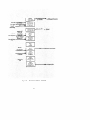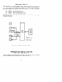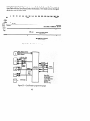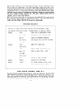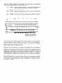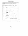
1
Foreword
This manual is for programmers and users of the Programmed Data
Processor-4, a high speed, stored program, digital computer manufactured by the Digital Equipment Corporation. Chapters 2 and 3 contain the
detailed information necessary to make use of the machine. Chapter 1
summarizes the machine’s electrical and logical design. Chapter 4 presents information helpful in making the electrical connections to inputoutput devices. Appendices provide detailed data which may be helpful
in specific programming assignments. Although program examples are
given in this document, no attempt has been made to teach programming
techniques. However, Appendix 4 explains the meaning and use of special
characters used in the programming examples.
Copyright
1962
Digital
Equipment
2
Corporation
Table
Of Contents
Page
CHAPTER
1: SYSTEM
DESCRIPTION
5
. . . . .._.._._...__...._._....
........................................
CHAPTER
2: ARITHMETIC
AND CONTROL
ELEMENT
..........................................................................................................
Functions
Control States ...................................................................................................
......................................................................................................
Instructions
11
11
.15
16
CHAPTER
3: INPUT-OUTPUT
EQUIPMENT
FUNCTIONS
AND PROGRAMMING
..2 5
25
....................................................................................
Input-Output
Commands
...........................................................................................
.25
Device Selector
.26
Information
Collector
...................................................................................
.28
Information
Distributor.
..................................................................................
28
Input-Output
Skip Facility
‘2:
Program
Interrupt
Control ................................................................................................................................................................................................................................
Input-Output
Status Instruction
...................................................................................................
29
Clock/Timer
(30
Input-Output
Devices
.......................................................................................
30
Precision
CRT Display, Type 30A ..................................................................
32
Light Pen, Type 32 ........................................................................................
.33
Precision CRT Display, Type 30D and Light Pen, Type 32 .............................
.34
Input Device) ......................
Converter
(Typical
High Speed Analog-to-Digital
35
Low Speed Analog-to-Digital
Converter
(Typical Input Device) ........................
36
................................................................................
Perforated-Tape
Reader
38
Printer-Keyboard
and Control,
Type 65 ........................................................
42
Type 75 ................................................
Perforated-Tape
Punch and Control,
44
Card Reader and Control, Type 41-4 ..............................................................
46
Card Punch Control, Type 40-4 ......................................................................
49
Automatic
Line Printer and Control,
Type 62 ................................................
CHAPTER
4: THE
Appendix
Appendix
Appendix
Appendix
Appendix
Appendix
Appendix
1
2
3
4
5
6
7
INTERFACE
ELECTRICAL
CHARACTERISTICS
.......................
Instruction
Lists .............................................................................
..............................................................................................
Codes
..................................................................
Read-In
Mode Sequence
..........................................................................
Assembly
Program
.......................................................
Multiply
and Divide Subroutines
Programming
Aids ...........................................................................
Powers of 2 ................................................................................
3
.52
57
61
65
67
7:O
73
..7 5
Typical
PDP-4
System
CHAPTER
SYSTEM
1
DESCRIPTION
Summary
The Digital Equipment Corporation Programmed Data Processor-4 (PDP-4)
is designed to be the control element in an information processing system.
PDP-4 is a single address, parallel, binary machine with an 18-bit word
length using l’s or 2’s complement arithmetic. Standard features of the
machine are stored program operation, a random access magnetic-core
memory, a complete order code, and indirect addressing.
Flexible, high-capacity input-output capabilities of
operate in conjunction with a variety of peripheral
forated-tape readers and punches, punched-card
Teletype printer-keyboard,
line printers, magnetic
analog-to-digital converters.
the PDP-4 enable it to
devices, such as perreaders and punches,
tape transports, and
The machine is completely self-contained, requiring no special power
sources, air conditioning, or floor bracing. From a single source of 115volt, 60cycle, single-phase power, PDP-4 produces circuit operating dc
voltages of -15 volts (%l) and +lO volts (&l) which are varied for marginal checking. Total power consumption is 900 watts. It is constructed
with standard DEC 4000 series system modules and power supplies.
Solid-state components and built-in marginal checking facilities insure
reliable machine operation.
System
Description
The basic PDP-4 system is shown diagramatically in Figure 1. Three po tions of the system are delineated according to function: the Arithmet c
and Control Element, the Interface, and the Input-Output Equipmen I .
Information originates not only from peripheral devices but can be entered
manually and modified at the Operator Console.
5
ARITHMETIC
------mm
-w-----m--
IMTERFACE
*Included in B
Standard PDP-4
Figure
1 -
PDP-4
ARITHMETIC
System
with
Real-Time
AND CONTROL
Connection
ELEMENT
The Operator Console, Internal Processor, and Core Memory constitute
the Arithmetic and Control Element. The Internal Processor carries out
the arithmetic and logical operations and controls the Real-TimeConnection and the Core Memory. Binary arithmetic with a fixed point is employed.
The optional Extended Arithmetic Control Unit, Type 22, gives PDP-4 a
multiply, divide, and arithmetic shifting capability without the use of subroutines.
The Console is used to observe and control the action of the program and
the Internal Processor, and to alter the contents of Internal Prncessor
registers. The contents of Core Memory can be examined or new inforAll Internal
Processor registers
are displayed
mation deposited.
continuously.
Memory capacities of from 1,024 to 32,768 words are available for PDP-4.
The cycle time (the time required to read information from memory and
rewrite information back into memory) is 8 microseconds. The access
time
(the time required to read information from memory) is 2 microseconds. In the event of power failure, the contents of the Core Memory
remain unaltered. See Chapter 2 for detailed functions of the Arithmetic
and Control Element.
INTERFACE
The Real-Time Connection, furnished as standard equipment, provides
communication between the Internal Processor and the Perforated-Tape
Reader, the Perforated-Tape Punch and Control, Type 75, and the Printer6
Keyboard and Control, Type 65. The Real-Time Option, Type 25 gives the
system the additional
capability
to operate efficiently
over a wide range
of information
handling rates (from seconds per event to 125,000 words
per second) and with a large variety of input-output
devices (see Figure 2).
The Real-Time
Option consists of a Device Selector, an Information
Collector, an Information
Distributor,
an Input-Output
Skip connection,
a
Program
Interrupt
facility, a Data Interrupt
facility, and a Clock/Timer.
See Chapter 3 for details of functions.
ARITHMETIC
AND CONTROL
ELEMENT
--w--------w-
PROCESSOR*
c-L-----------e---II
INTERFACE
I
I
-m-s-..-
INPUT-OUTPUT
EDUIPMENT
I
CARD
Ill
READER
I
III
I
I
?
TYPE
TYPE
*included
in a
I
RELAY
40.4
62
BUFFER,
I
Equipment
Figure
2 -
PDP-4
System
with
Real-Time
Option
THE DEVICE SELECTOR consists of decoding elements to select and
establish the state of an external device when the program issues an
input-output
transfer instruction.
The direction of information
transfer
(in or out of the Internal Processor) is controlled
by signals produced
by the Device Selector. Up to 64 input-output
devices can be selected
and these, in turn, may cause the selection of many more. The standard Device Selector has provisions for twenty selector elements.
THE INFORMATION
COLLECTOR
receives
information
from input
devices (selected by the Device Selector) and transfers the information to the Internal Processor.
Up to 18 bits of information
can be
collected simultaneously;
8 x 18 bits of information
may be collected,
broken into variable-sized
words.
7
I
I
1
.
The
Perforated-Tape
Reader
(top)
8
and
Printer-Keyboard
(bottom).
THE INFORMATION DISTRIBUTOR distributes information from the
Internal Processor to all output devices. Only the output device selected (or addressed) by the Device Selector samples and reads in
the information contained in the Information Distributor. Up to 8 x 18
bits may be distributed.
THE INPUT-OUTPUT SKIP CONNECTION provides a program skip
instruction conditioned by the state of a given input-output device
logic line. The instruction following the skip instruction will not be
executed if the line is a 1. Eight skip conditions may be sampled.
THE PROGRAM INTERRUPT permits one of 11 lines (conditions) or
input-output devices to interrupt the program and initiate a subroutine which may return to the original program when the cause for
interruption has been processed. The machine state is preserved
during a Program Interrupt. This type of interrupt is suited for information or event rates in the range of 0 to 2,000 cycles per second.
THE DATA INTERRUPT allows a device to automatically interrupt the
program and deposit or extract data from the Core Memory at an
address specified by the device. The Data Interrupt is suited for high
speed information transfers; up to 125,000 18-bit words may be
transferred per second.
THE CLOCK/TIMER produces a signal which increments a Core Memory register at a rate of 60 cycles per second. When the register overflows, a Program Interrupt occurs.
INPUT-OUTPUT
DEVICES
All of the input-output devices are optional except the Perforated-Tape
Reader.
THE PERFORATED-TAPE READER senses 5-, 7-, or 8-hole perforatedtape at the rate of 300 lines per second. Either one line of tape (alphanumeric) or 3 lines of tape (binary word) may be read.
THE PERFORATED-TAPE PUNCH AND CONTROL, TYPE 75, perforates 5-, 7-, or 8-hole paper tape at a rate of 63.3 lines per second.
THE PRINTER-KEYBOARD AND CONTROL, TYPE 65, includes a
Teletype Model KSR-28 Printer and Keyboard with an allowable input
or printing rate of ten characters per second. Typed information may
be monitored by a program. A program may print information.
THE PRECISION CRT DISPLAY, TYPE 30, displays data on a 9%” by
9%” area. Information is plotted point by point to form either graph cal
or tabular data. Operation of this device requires the Real-Time Opti k n.
THE LIGHT PEN, TYPE 32, is a photoelectric device which det cts
information displayed on the Type 30 Visual CRT Display. Upon si nal
9
from the Light Pen, the computer carries out previously programmed
instructions. Requires Real-Time Option.
THE 18-BIT RELAY BUFFER, TYPE 67-4, provides contacts which
operate devices of higher power rating. The relays have form “D”
contacts, which open and close in approximately 3 milliseconds.
Requires Real-Time Option.
THE PROGRAMMED MAGNETIC TAPE CONTROL, TYPE 54,
up to four Magnetic Tape Transports, Type 50. Information
from or written on the tape. The format on the tape may
grammed to be compatible with IBM tapes having a density
6 + 1 bit characters per inch. Requires Real-Time Option.
controls
is read
be proof 200,
THE MAGNETIC TAPE TRANSPORTS, TYPE 50, are used with the
Programmed Magnetic Tape Control, Type 54.
THE AUTOMATIC LINE PRINTER AND CONTROL, TYPE 62, operates
at up to 600 lines per minute, 120 columns per line. Each column
may print one of 64 characters. Spacing format is controlled by a
punched format tape in the Printer. Once a command to print or space
is given, the Internal Processor is not required. Approximately one
per cent of program running time is required to operate the Line
Printer at a 600~line-per-minute rate. Requires Real-Time Option.
THE CARD READER AND CONTROL, TYPE 41-4, operates at a rate of
up to 200cards per minute. Cards are read column by column. Column
information may be read in alpha-numeric or binary mode. The alphanumeric mode converts the 12-bit Hollerith Code of one column into
the six-bit binary-coded decimal code with code validity checking.
The binary mode reads a 12-bit column directly into the PDP-4. Approximately one per cent of a Card Reader program running time is
required to read the 80 columns of information at the 200 cards per
minute rate. Requires Real-Time Option.
THE CARD PUNCH CONTROL, TYPE 40-4, enables the operation of a
standard IBM Type 523 Summary Punch with PDP-4. Cards are
punched row by row at a rate of 100 cards per minute. Approximately
0.3 per cent of program running time is required to operate the Card
Punch at the lOO-card-per-minute
rate. Requires Real-Time Option.
PROGRAMMING
AIDS
Several programs are supplied with each PDP-4 to assist the programmer
in routine tasks. They include: The PDP-4 Assembly Program, the DDT-14
debugging tape, double-precision floating point routines,
routines, a tape reproducer, punch routines, an octal
an algebraic compiler, and a floating point functions
enable various functions, such as double precision floating-point sine,
be computed. See Appendix 6.
10
CHAPTER
ARITHMETIC
AND
2
CONTROL
ELEMENT
In this chapter the functions
of the Arithmetic
and Control Element are
described
in detail. The operations
of the machine
instructions
are explained and listed.
Functions
INTERNAL
PROCESSOR
The Internal Processor performs
arithmetic
operations,
controls memory
access, and handles information
entering
and leaving the machine.
It
consists of the Information
Processor Control, which oversees all activities,
and six registers: Accumulator,
Link, Memory
Buffer, Memory Address,
Instruction,
and Program Counter. The elements of the Internal Processor
are shown within the broken line in Figure 3.
Data Interrupt
address
and
data lines to
e
and from external
devices,
under
control
of Real
Time Option
I
I
r ---I
data
lines
from
I
ACCUMULATl
SWITCHES,
L’
Normal
transfer
to and
I
(Of
C
___.
ACCUMULATOR
18
PROGRAM
COUNTER
4
13
REGISTER
BUFFER
Option
(of
or under
1
KEYS
Operator
Console)
I
,
f
-
(control states.
INTERNAL
PROCESSOR
L
--3--v-
timing,.etc.)
-----c--Be
Figure
3 - Arithmetic
and Control
11
Element
ACCUMULATOR (AC): Arithmetic operations are performed in this
18-bit register. The AC may be cleared and complemented. Its contents may be rotated right or left with the Link. The contents of the
Memory Buffer may be added to the contents of the AC with the result
left in the AC. The contents of both these registers may be combined
by the logical operations AND and Exclusive OR, the result remaining
in the AC. The Inclusive OR may be formed between the AC and the
Accumulator Switches on the Operator Console (see below), and the
result left in the AC.
The Accumulator also acts as an input-output register. Under normal
operation all information transfers between core memory and an
external device must pass through the Accumulator.
LINK (L): This is a one-bit register used to extend the arithmetic
facility of the Accumulator. In l’s complement arithmetic, the Link
is an overflow indicator; in 2’s complement it functions as a carry
register. The Link may be cleared and complemented and its state
sensed independent of the AC. It is included with the AC in rotate
operations.
MEMORY BUFFER (MB): All information transferred between Core
Memory and the AC, Instruction Register, or Program Counter passes
through the MB. Information is read from a memory cell into the MB
and rewritten into the cell in one cycle time (8 microseconds). Instructions are brought from memory into the MB to be decoded. The
MB serves also as a buffer for information transferred between Core
Memory and an external device in a Data Interrupt. The contents of
the MB may be incremented by one.
MEMORY ADDRESS REGISTER (MA): The address of the Core Memory
cell currently being accessed is contained in the 13-bit MA. Information may enter the MA from the MB, Program Counter, or from an
external device operating in a Data interrupt.
INSTRUCTION REGISTER (IR): This is a 4-bit register which contains
the operation code of the instruction currently being performed by
the computer. Information enters the IR from the MB.
PROGRAM COUNTER (PC): The program sequence, that is, the order
in which instructions are performed, is determined by the PC. This
13-bit register contains the address of the memory cell from which
the next instruction will be taken. Information may enter the PC from
the MB, MA, or the Address Switches of the Operator Console.
12
MEMORY
The memory contains stored information for processing, and the instructions of the program being run. Memory capacities of from 1,024 to 32,768
words are available in PDP-4. Standard models PDP-4A and PDP-4B come
with 1024-word and 4096-word memories, respectively. The two models
are identical in all other respects. The smaller memory has a 32 by 32 by
18 core array, the larger a 64 by 64 by 18 core array. A Memory Module
Type 17, containing a 64 by 64 by 18 core array may be added to PDP-4B
to give it an 8192-word capacity. With the addition of the Magnetic Core
Memory Extension Control Type 16, memory modules may be added to
build a memory of 32,768 words. Further increase in storage capacity can
be gained by adding the Magnetic Drum System Type 24, available in
three capacities: 16,384, 32,768, and 65,536 words.
OPERATOR
CONSOLE
The Operator Console contains all the switches and controls necessary to
run the machine, and lights which indicate the current status of the Internal Processor. The functions of the lights and controls are described
in the following tables.
Figure 4 - Operator Console
13
Console Switches
Function
ADDRESS
A group
of 13 switches
which
establishes
the memory
address
for the START,
EXAMINE, and DEPOSIT operations.
ACCUMULATOR
A group of 18 switches,
the setting of which
determines
the word to be placed in memory
by the DEPOSIT and DEPOSIT NEXT operations,
or to be placed
in the AC under
program
control.
POWER
Controls
the primary
power to the computer
and all external
devices attached
to it.
SINGLE
STEP
Causes the computer
to stop at the completion of each memory
cycle. Repeated
operation of CONTINUE
while this switch
is on
will step the program
one cycle at a time.
SINGLE
INSTRUCTION
Causes the computer
to stop at the completion of each instruction.
Repeated
operation
of CONTINUE
while this switch
is on will
step the program
one instruction
at a time.
When both switches
are on, SINGLE STEP
takes
precedence
over SINGLE
INSTRUCTION.
REPEAT
Causes the operations
initiated
by pressing
CONTINUE,
EXAMINE
NEXT, or DEPOSIT
NEXT, to be repeated
as long as the key is
held on. The rate of repetition
is controlled
by the setting of the SPEED knobs.
SPEED
Two controls
that vary the REPEAT interval
from approximately
40 microseconds
to 8
seconds.
The left knob
is a five-position
coarse control,
the right knob a continuously
variable fine control.
For both knobs, slowest
speed is obtained
in extreme
left position.
Console Light
Indication
ACCUMULATOR
The contents
of the AC.
MEMORY
The contents
of the MB.
The contents
of the Link.
The contents
of the MA register.
The contents
of the
The contents
of the PC.
BUFFER
LINK
MEMORY
ADDRESS
INSTRUCTION
PROGRAM
COUNTER
The computer
RUN
FETCH,
DEFER,
EXECUTE,
BREAK
The primary
ory cycle.
14
IR.
is executing
control
state
instructions.
of the
next
mem-
Console Key
Function
START
Starts the processor.
The first instruction
is
taken
from
memory
cell specified
by the
setting
of the ADDRESS.
switches.
The
START operation
clears the AC and Link,
and turns off the Program
Interrupt.
STOP
Stops the processor
at the completion
memory
cycle in progress
at the time
operation.
CONTINUE
Causes the computer
to resume
operation
from the point at which it was stopped
by
the last previous
operation
of STOP or one
of the EXAMINE
or DEPOSIT keys. Besides
the normal off and momentary
on positions,
CONTINUE
has a latched
on position
obtained
by ralsing
the key instead
of depressing
it.
EXAMINE
Places
the contents
of the memory
cell
specified
by the ADDRESS
switches
in the
AC and MB. The contents
of the ADDRESS
switches
appear
in the MA. The PC contains
the address
of the next cell.
EXAMINE
Places the contents
of the cell specified
the PC in the MB and AC. The C(PC)
incremented
by one. The MA contains
address
of the register
examined.
NEXT
DEPOSIT
DEPOSIT
of the
of key
by
are
the
Deposits
the contents
of the AC switches
in
the memory
cell specified
by the ADDRESS
switches.
The C(AC switches)
remain
in the
AC and MB. The contents
of the ADDRESS
switches
appear in the MA. The PC contains
the address
of the next cell.
NEXT
Deposits
the contents
of the AC switches
in
the memory
cell specified
by the PC. The
C(PC) are then incremented
by one. The
C(AC), C(MB),
and C(MA) are the same as
for DEPOSIT.
Control
States
The POP-4 operates in one of four primary control states during a memory
cycle: Fetch, Defer, Execute, or Break. The next control state is established
at the completion of the current one. All states except Break are deter.
mined by the instructions themselves.
FETCH: A new instruction is obtained when this state occurs. The
contents of the memory cell specified by the PC are placed in the MB,
15
and the instruction
part (bits O-4) of this word
The C(PC) are then incremented
by one.
are placed
in the IR.
If a two-cycle instruction
is fetched, the following control state will be
either Defer or Execute.
If a one-cycle
instruction
is fetched,
the
operations
specified
will be performed
during the last part of the
Fetch cycle. The next state will be Fetch.
DEFER: When bit 4 of a memory referehce instruction
is a 1, the Defer
state is entered to perform the indirect addressing.
The process of
indirect addressing
is often referred to as deferring,
in the sense that
access to the operand is deferred once to another memory cell. This
is why the primary control state in which this operation is performed
is called Defer. Bit 4 of a memory reference instruction
is referred to
interchangeably
as the Indirect or the Defer Bit.
EXECUTE: This state is established
only when a memory
reference
instruction
is being performed.
The contents
of the memory
cell
addressed
are brought into the MB, and the operation
specified
by
the C(IR) is performed.
BREAK: When this state is established,
the sequence
is broken for a Data Interrupt
or a Program Interrupt.
the break occurs only at the completion
of the current
of instructions
In both cases,
instruction.
The Data Interrupt
allows information
to be transferred
between
memory
and an external device; when this transfer
has been completed, the program sequence is resumed from the point of the break.
The Program Interrupt causes the sequence to be altered. The C(PC)
and the C(L) are stored in location 0000 and the program continues
from location 0001.
Instructions
The instruction
of instructions:
code is specified by bits O-3 of a word. There are two types
Memory Reference and Augmented.
MEMORY
REFERENCE
INSTRUCTIONS
The bit assignment
of the memory reference instruction
is shown in Figure
5. Bits O-3 determine
the operation to be performed.
Bits 5-17 specify the
address of the memory cell containing
the operand.
If bit 4 is a 1, then
indirect addressing
occurs. In the following discussion,
i is the mnemonic
symbol used to indicate indirect addressing.
16
01
1121314151617
~8~9~10~11~12~13~14~15~16~17
vvt1
Operation Indirect
Code
Address
(Defer)
Figure
5 -
Operand Address
Memory
INDIRECT
reference
instruction
format
ADDRESSING
When indirect addressing
is specified,
the address part (bits 5-17) of a
memory reference instruction
is interpreted
as the address of a cell containing not the operand,
but the address of the operand.
Consider the
instruction
add A. Normally,
A is interpreted
as the address of the cell
containing
the quantity be be added to the AC. Thus, if cell 100 contains
the number 576, the instruction
add
100
will cause the quantity 576 to be added to the AC. Now suppose
576 contains the number 1135. The instruction
add
that cell
i 100
(where i signifies indirect addressing)
will cause the computer
to take the
number 576, which is in cell 100, as the effective address of the instruction,
and the number
in cell 576 as the operand.
Hence this instruction
will
result in the quantity 1135 being added to the AC.
If, when indirect addressing
is indicated,
the memory cell addressed
by
the instruction
is one of those in locations 10-17, the contents of that cell
are incremented
by one and the result taken as the effective
address.
This feature is called auto-indexing.
If memory cell 12 contains the number
200, the instruction
add i 12
will cause the number
in cell 200 + 1 to be added to the AC.
1’S COMPLEMENT
ARITHMETIC
When two numbers
are added together
in l’s complement
arithmletic
(see add instruction
in following table), a 1 carried out of the high-order
position will be added to the low-order digit, as follows:
rl
110101001100011
011001010111101
001110100100000
00111010010000~
17
Since bit 0 of a word is used for the sign of a number, the largest positive
number that can be represented is 217-l. If, in l’s complement addition,
the addends are of like sign and the sign of the sum is different, overflow
is said to have occurred and the Link is set to 1.
2’S COMPLEMENT ARITHMETIC
In 2’s complement addition (see tad instruction), a carry out of the highorder bit is not added into the low order position. Instead, if a carry occurs,
the Link is complemented.
The signs of the addends and sum are not
examined. Two’s complement
addition is used primarily in multiple
precision arithmetic.
All memory reference instructions require an Execute cycle (see Control
States above) to transfer data between Core Memory and the MB and
execute the instruction. When indirect addressing is specified, an extra
cycle is required to determine the effective address. The jmp instruction,
while it requires an address, does not require an operand; an Execute
cycle is thus not needed, and the instruction is performed in only one cycle.
MEMORY REFERENCE INSTRUCTIONS
Explanation
C(A)
A =>
Yl-4
Y,
MNEMONIC
SYMBOL
B
of Special
contents
of A
A replaces
B
bits 1 - 4 of Y
a given bit in Y
aL
V
A
ii
%iz-
(BITS
~
O-3)
Terms
TIME
(w=>
~~.~
exclusive
OR
inclusive
OR
AND
l’s complement
of A
OPERATION
lac Y
20
16
Load AC. The C(Y) are loaded
The previous
C(AC) are lost.
C(Y) => C(AC).
dac Y
04
16
Deposit
AC. The C(AC) are deposited
in
the memory
cell at location Y. The previous
C(Y) are lost; the C(AC) are unchanged.
C(AC) => C(Y).
dzm
Y
14
16
Deposit Zero in Memory.
in memory
cell Y. The
lost. The AC is unaffected
0 => C(Y).
add Y
30
16
Add (l’s complement).
The C(Y) are adde
to the C(AC) in l’s complement
arithmeti
The result is left in the AC and the origin
C(AC) are lost. The C(Y) are unchange
The Link is set to 1 on overflow.
(See text t
C(Y) + C(AC) => C(AC).
18
into the AC.
Zero is deposited
original
C(Y) are
by this operation.
.
I
.
.
MNEMONIC
SYMBOL
tad Y
xor Y
OCTAL
CODE
(BITS O-3)
34
24
TIME
(b-c)
16
16
OPERATION
Two’s
complement
Add.
The C(Y) are
added
to the C(AC) in 2’s complement
arithmetic.
The result is left in the AC and
the original
C(AC) are lost. The C(Y) are
unchanged.
A carry out of the 0 bit corn:
plements
the Link.
C(Y) + C(AC) => C(AC).
Exclusive
OR. The logical
operation
Exclusive OR is performed
between
the C(Y)
and the C(AC). The result is left in the AC
and the original
C(AC) are lost. The C(Y)
are unchanged.
Corresponding
bits are
compared
independently.
C(Yj) V C(ACj) => C(ACj).
Example
C(AC)j
and Y
50
16
original
0
0
1
1
C(AC)i
W>i
0
final
0
1
1
0
A
1
AND. The logical
operation
AND is performed
between
the C(Y) and the C(AC).
The result is left in the AC, and the original C(AC)
are lost.
The C(Y) are unchanged.
Corresponding
bits are compared independently.
C(Yj) A C(ACj) => C(ACj)
Example
C(AC) jrnal
sad Y
54
16
1 Cr
1 C(ACi
Skip if AC is Different
from Y.
are compared
with the C(AC). If
bers are the same, the computer
to the next instruction.
If the
are different,
the next instruction
ped. The C(AC)
and the C(Y)
changed.
If C(AC) # C(Y) then C(PC) + 1 =>
19
final
The C(Y)
the numproceeds
numbers
is skipare unC(PC).
MNEMONIC
SYMBOL
OCTAL
CODE
(BITS O-3)
TIME
(ec)
is2 Y
44
16
Y
60
8
jms Y
10
16
Jump to Subroutine.
The C(PC) and the
C(L) are deposited
in memory
cell Y. The
next instruction
is taken from cell Y + 1.
C(L) => C(Y,). 0 => C(Y,,).
cal
00
16
Call Subroutine.
The address
portion
of
this instruction
is ignored.
The action
is
identical
to jms 20. The instruction
cal i is
equivalent
to jms i 20.
xct Y
40
iv
OPERATION
Index and Skip if Zero. The C(Y) are incremented
by one in 2’s complement
arithmetic.
If the result
is 0, the next
instruction
is skipped.
If not, the computer
proceeds
to the next instruction.
The C(AC) are unaffected.
C(Y) + 1 => C(Y).
If result = 0, C(PC) + 1 => C(PC).
Jump
to Y. The
executed
is taken
Y => C(PC).
C(PC)
8 + time
of instruction
being
executed
AUGMENTED
=>
next
from
instruction
to be
memory
cell Y.
C(Y&17). Y + 1 => C(PC).
Execute.
The instruction
in memory
cell Y
will be executed.
The computer
will act as
if the instruction
located
in Y were in the
place of the xct.
INSTRUCTIONS
None of the augmented
instructions
require a memory
reference.
Bits
4-17 of an augmented
instruction
are used to specify operations,
many
of which may be combined
in a single instruction.
There are three classes
ot augmented
instructions:
a. Operate class: includes o.perations
group, and the halt instruction.
b. The special
instruction,
on the AC and
Link,
the skip
law.
c. Input-output
transfer
class: includes
all the instructions
which
initiate transfers
of information
between the Internal Processor and
an external device and those that sense the status of the devices.
20
OPERATE
CLASS
The instructions
of the Operate class require one cycle for their execution.
The octal code (bits O-3) for this class is 74. The operations
specified by
bits 4-17 are called micro-instructions.
The functions
of each microinstruction
are described
in the following table. The Event Time indicates
when the operation
is performed
in the course of the cycle. Times 0, 1,
and 2 occur in that order in the latter part of the cycle.
Except for the restrictions
indicated
at the end of the table, microinstructions
may be combined
in a single instruction.
The bit assignment
of the Operate class micro-instructions
is shown in Figure 6.
Opr-740000
Invert
Sense
Of Skip
1 If bit 8=1
5 16 1 7 181
ttt
da
If bit 7 = 1
9 1101 11 ~12~13~14~15~16~17
ttttttttt
cl1
snl sza sma hlt rar ral oas cml cma
I
Additional
Rotate
Figure
MNEMONIC
SYMBOL
OCTAL
CODE
6 -
Operate
class
instruction
-
EVENT
TIME
bit assignment
OPERATION
opr
740000
cla
750000
2
Clear AC. The AC is cleared
0 => C(AC).
cma
740001
3
Complement
AC.
plemented.
C(AC) => C(AC).
cll
744000
2
Clear
0 =>
cml
740002
3
Complement
Operate.
Indicates
the Operate
class. When
used
alone,
performs
no operation;
the
computer
proceeds
to the next instruction.
21
Link.
C(L).
Link
Each
to 0.
bit of the
is set to 0.
Link.
C(L) => C(L).
AC is com-
MNEMONIC
SYMBOL
OCTAL
CODE
EVENT
TIME
OPERATION
ral
740010
3
Rotate
rotated
C(ACJ
C(AC,)
AC
left
=>
=>
Left. The C(AC) and the
one place.
C(AC j-~)
C(L).
C(L) => C(AG7)
rtl
742010
2, 3
Rotate
Two places
successive
ral’s.
rar
740020
3
Rotate AC Right. The C(AC)
rotated
one place right.
C(ACj) => C(ACj-1)
C(L) => C(ACo)
C(AC17) =>C(L)
rtr
742020
2, 3
Rotate
Two
Places
Right.
equivalent
to two successive
oas
740004
3
OR AC Switches.
The Inclusive
OR of the
C(AC) and the C(AC switches)
is placed in the
AC. A switch
up is interpreted
as a 1.
C(AC Switches)
V C(AC) => C(AC).
Left.
C(L)
Equivalent
and
are
to two
the C(L) are
Action
rar’s.
taken
is
Example
C(AC) jrnal
1 Cr
/ C(AC[
final
sma
740100
1
Skip if Minus AC. If the AC is negative,
next instruction
is skipped.
If AC0 = 1, then C(PC) + 1 => C(PC).
the
spa
741100
1
Skip if Plus AC. If the AC is positive,
the
instruction
is skipped.
If AC0 = 0, then C(PC) + 1 => C(PC).
next
sza
740200
1
Skip if Zero AC. If C(AC) are 0, the next
struction
is skipped.
If C(AC) = 0, then C(PC) + 1 => C(PC).
sna
741200
1
Skip if Non-zero
AC.
If C(AC) # 0, then C(PC)
22
+ 1 => C(PC>.
in-
MNEMONIC
SYMBOL
snl
szl
OCTAL
CODE
740400
741400
EVENT
TIME
OPERATION
1
Skip if Non-zero
Link.
instruction
is skipped.
If C(L) # 0, then C(PC)
1
Skip if Zero
740040
immediHalt.
ately after
the completion of the
cycle.
Stops
is 1, the
+ 1 =>
C(PC).
+ 1 =>
C(PC).
next
Link.
If C(L) = 0, then
hlt
If C(L)
C(PC)
the computer.
If skips are combined
in a single instruction,
ditions to be met will determine
the skip. For
are indicated (octal code 740600), the next
either the AC is zero or the Link is non-zero,
the Inclusive OR of the coninstance, if both sza and snl
instruction
will be skipped if
or both.
If ral or rar is specified, cma, cml, oas may not be specified, and conversely.
If rtl or rtr is specified,
cma, cml, cla, cll, oas may not be specified,
and
conversely.
THE INSTRUCTION,
law
The octal code for this instruction
is 760000. Bits 5-17 are used to specify
a quantity to be placed in the AC. The effect of the law instruction
is to place
itself in the AC.
law Y
76
8 psec
Load
INPUT-OUTPUT
The instructions
in this class
between the Internal Processor
iot
760000
8 psec
AC With
law Y.
TRANSFER
CLASS
are used to effect information
transfers
and external devices, via the Interface.
Input-Output
Transfer.
Bits 4-13 of an iot
instruction
determine
the device
and subdevice to be selected.
The presence
of a 1 in
bit 14 will cause
the AC to be cleared
at
hen
Event
time
1. Bits 15-17
determine
pulses are to be sent to the selected
de1 ice.
The bit assignment
of the iot instruction
is shown
tions of the iot class are described in Chapter 3.
23
in Figure 7. The instruc-
Operation
Code
Sub-Device
Selection
Device
Selection
Sob-Device
Selection
,&$qfyhJl
0
1
2
If Bit Is a 1:
3
4
5
6
7
8
9
10
11
12
13114115116[17
Clear AC at event time 1
Transfer an IOT pulse at event time 3
Transfer an IOT pulse at event time 2
Transfer an IOT pulse at event time 1
Figure
7 -
Bit assignment
for input-output
24
transfer
instruction
(iot)
CHAPTER
INPUT-OUTPUT
FUNCTIONS
AND
3
EQUIPMENT
PROGRAMMING
PDP-4 is capable of operating with the ten input-output devices described
in Chapter 1 and with a variety of others. The computer can operate with
most of the devices simultaneously. The Interface, consisting of the RealTime Connection or the Real-Time Option, issues commands to the devices,
monitors their state of availability, transfers information to them, and
receives information from them. Since the Internal Processor can store
or read out data much faster than the devices can operate, the Interface
and the individual devices provide buffering to minimize the amount of
program time consumed in transfers.
The Real-Time Connection, furnished as standard equipment, provides
communication between the Internal Processor and the Perforated-Tape
Reader, the Perforated-Tape Punch, and the Keyboard-Printer. The RealTime Option, Type 25, gives the system the additional capability to operate
efficiently over a wide range of information handling rates, from seconds
per event to 125,000 words per second, and with a large variety of inputoutput devices. The Real-Time Option consists of the Device Selector, the
Information Collector, the Information Distributor, the Input-Output Skip
Facility, the Program Interrupt Control, the Data Interrupt Control, and
the Clock/Timer (see Figure 8).
The coupling of input-output equipment to PDP-4 is similar for all devices.
The electrical characteristics of the coupling are discussed in Chapter 4.
The logical functions and programming instructions are given below.
Input-Output
DEVICE
Commands
SELECTOR
(DS)
The input-output transfer (iot) augmented instruction causes the Interface
to produce pulses which select IO devices and transfer information. Upon
receipt of an instruction, the Device Selector in the Interface performs one
of the following functions:
(a) Starts a device (e.g.asks for a line of perforated tape to be read and
assembled into a word, a card to be moved to a reading or punching
station, etc.)
25
(b) Transfers data from the information buffer of an input device to
the AC, through the Information Collector
(c) Transfers information from the AC, through the information
tributor to the buffer of an output device
(d) Senses the flag(s) associated with a device to determine
ability
Dis-
its avail-
(e) Resets the flags. These commands dismiss a device without asking
for additional action.
The flags referred to above are signals generated by an external device
upon completion of its assigned task. This technique allows the Internal
Processor to resume its arithmetic operations after issuing an instruction
to a relatively slow input-output device (data rate of less than 20,000
words per second). When a flag is set to 1 by the device, it signifies that:
(a) an output action (punch out, etc.) has been completed; the Arithmetic and Control Element may transmit data to the device.
(b) an input action (card or tape input, etc.) has occurred; information
is available for the Arithmetic and Control Element.
(c) an alarm condition exists.
Flags may be sensed, and a program skip take place, using the Output
Skip Facility (see below). Flags may be read into the AC using the iors (in-out
read status) instruction. Most flags are connected to the Program Interrupt
(see below).
The Device Selector selects an input-output device or subdevice according
to the address code of the device in bits 4-13 in the iot instruction. It then
generates IO pulses at event times 0, 1, and 2 if the appropriate microinstruction code bits are present in bits 17, 16, and 15. Pulse iot 0 occurs
near the end of an iot instruction, followed by iot 1 in 2 microseconds.
Pulse iot 2 occurs at the beginning of the next instruction, 1.2 microseconds
after iot 1. This timing enables one iot instruction to perform multiple
operations.
INFORMATION
COLLECTOR
(IC)
The Information Collector enables information to be collected from eight
l&bit word input devices. The AC must contain 0 at the time the inputs are
sampled. A word can be broken into smaller words according to the word
size requirements of the input device. The program steps for reading the
contents of a group of static parallel data bits are:
cla
iot
Clear the AC (AC must equal 0)
dac Y
Deposit C(AC). The C(AC) are sent to a particular
(the first two steps may be microprogrammed
struction)
Selected
device
(sample
the selected
26
device
outputs)
memory
together
cell, Y.
in one in-
DISTRIBUTOR
Requests
From
(11)
IO Device
Flags
4
INTERRUPT
Data
)
Request Acknowlaged
INTERRUPT
!&I& oirection
DATA
INTERRUPT
ADDRESS
-
18 Addreas
DATA
INTERRUPT
INFORMATION
(W
Figure
8 -
-0
Real Time
27
Option,
Type
25
18 Outgoing
Data
INFORMATION
DISTRIBUTOR
(ID)
The Information
Distributor
presents the static data contained
in the AC
to each output device requiring AC information.
The devices sample the
Information
Distributor
using the program-controlled
pulses from the
Device Selector. The program steps for transmitting
information
from a
particular
memory cell are:
lac Y
Load
the AC with
iot
Clear
selected
iot transmit
The information
is sampled
and placed in the register
of the
input-output
device.
(the second
two steps may be microprogrammed
together
in one instruction)
C(Y)
output
INPUT- OUTPUT
register
SKIP
to prepare
FACILITY
for information
(10s)
The Input-Output
Skip facility enables the program to skip (or branch)
according to various external device states. There are eight inputs to the
Skip facility. The iot pulses from the Device Selector strobe an input line
and if a logic condition is present, the instruction
following the iot is skipped.
The iot skip pulse must occur at event time 1.
PROGRAM
The program interrupt
It is used to speed the
to allow certain alarm
terrupt may be enabled
INTERRUPT
CONTROL
(PIC)
allows a logic line state to interrupt
the program.
processing
of input-output
device information,
or
conditions
to be sensed by the computer.
The inor disabled by the program.
When the interrupt
occurs, the contents of the Program Counter
Link are stored in memory
location 0 (bits 0, 5. . . 17) and an
program begins in memory location 1. This action disables the
mode. The interrupt
program is responsible
for finding the signal
the interruption,
for removing
the condition,
and for returning
original program.
and the
interrupt
interrupt
causing
to the
When the condition for interruption
is removed, an iot signal to re-enable
the Program Interrupt
is given, followed by the instruction,
jmp indirect 0,
or 620000. The interrupt
program will then resume. If a Program Interrupt
request is waiting, it will be serviced after the 620000 instruction.
If a
second interruption
condition occurs and the Interrupt program is running,
the signal will have no effect; that is, there is only one level of interruption.
The START key disables the Program Interrupt system. The iot instructions
for the program interrupt are:
iof
-
700002
-
Disable
the
Program
Interrupt
ion -
700042
-
Enable
the
Program
Interrupt
28
INPUT- OUTPUT
STATUS
INSTRUCTION
The iors (in-out read status) instruction, 700314, enables the status of all
IO devices to be read into the AC and sampled. Various IO device states
are indicated by the presence of a 1 or 0 in the bit positions allocated for
that device (see Figure 9).
Program
Interrupt
Tape
On
Reader
Flag
Tape
Punch
Flag
Keyboard
Input
Type-Out
Display
Clock
Overflow
Flag
Card
Punch
Malfunction
Flag
Card
Punch
Row
Flag
Card
Reader
End
Flag
Card
Reader
Malfunction
Clock
Enabled
Tape
Interrupt
Magnetic
of File
Switch
-
x = Program
Figure
Flag
9 -
Input-Output
Interrupt
Status
Connected
instruction,
bit assignment
CLOCK/TIMER
The Clock produces a pulse every l/60 second (16.6 milliseconds) which
temporarily interrupts the program (in the same manner as the data
interrupt) and a 1 is added to the contents of memory cell 7 using 2’s
complement addition. If the contents of memory cell 7 are 0 after the
addition, the Clock flag is set to 1, which initiates a Program Interrupt if
the Interrupt is on. Depressing the START key on the Operator Console
clears the Clock flag and disables the Clock. The iot instructions associated
with the Clock are:
csf
-
700001
-
Skip the next
instruction
if the Clock
flag is a 1
cof
-
700004
-
Disable
the Clock
and clear
the Clock
flag
con -
700044
-
Enable
the Clock
and clear
the Clock
flag
Register 7 is identical to other core memory registers, that is, its contents
may be examined or modified. By presetting register 7 to a number, a
Program Interrupt will occur when the register overflows after a timed
interval.
29
Input-Output
Devices
All of the Input-Output
Devices discussed
below can be controlled
by the
Real-Time
Option, Type 25. The Real-Time
Connection,
furnished
as
standard
equipment,
provides communication
between the Internal Processor and the Perforated-Tape
Reader, the Perforated-Tape
Punch and
Control, and the Printer-Keyboard
and Control. All devices except the
Perforated-Tape
Reader are optional. This section is arranged in the order
of increasing complexity
of connection.
PRECISION
CRT DISPLAY,
TYPE 30A
Data points are displayed
on a 9% inch by 9% inch area. Information
is
plotted point by point to form either graphical or tabular data. Two digitalto-analog converters
drive the deflection
yokes in the X and Y directions.
Data can be plotted at a 20 kc rate, or every 50 miscroseconds.
The program loads the AC with a point to be plotted. Bits 0 through 8 specify
the X co-ordinate
of the point and Bits 9 through 17 the Y co-ordinate.
The
C(AC) are then transferred
to the Display Buffer. The specifying
of the
point initiates the plotting of the point on the CRT.
DRECISIOI\
TYPE
30A
Status Sits:
NOM
PIG
Program Interrupt:
NOW2
cl
Figure
10 -
Precision
CRT Display,
30
Type
30A programming
logic
The CRT, Type 30A is selected when the numbers 0 and 5 (octal) are specified in bits 8 and 9 respectively, of the iot instruction. The display commands are:
dls -
700506
-
Load the Display Buffer and select the display.
The program
loads the Display
Buffer from the AC. A point is plotted
as
specified
by the C(Display
Buffer).
The plotting
requires
50 microseconds,
after which another
dls can be given. The
Light Pen flag or Display flag is cleared with dls.
700502
- Clear
700504
- C(AC)
V C(Display
Buffer)=>
point specified
by the C(Display
the X and Y display
buffers.
0 =>
C(Display
C(Display
Buffer).
Buffer).
Buffer).
Plot
the
The points specified in the AC are plotted as unsigned quantities, beginning
in the lower left hand corner of the cathode ray tube. The point locations are:
400377
.
. 377377
--r
2g points
400400
.
. 377400
L
A program sequence is given in PDP-4 Assembly language below. The
program begins in register 40, and plots a point, XY, as specified by Core
Memory register 10.
PROGRAM SEQUENCE
/display
a point
30a
lO/
,..
/xy bits
40/
lac 10
/place
O-8, bits
xy co-ordinate
/display
/must wait
31
g-17 y.
the point,
in ac
next dls command
50 microsec.
LIGHT
PEN, TYPE 32
The Light Pen is a photosensitive
device which detects the presence of
information
displayed on a CRT. If the Light Pen is held in front of the CRT
at a point displayed, the Display flag will be set to a 1. The Pen is specified
by 0 and 5 in bits 8 and 9 of the iot instruction.
The commands
are:
dsf -
700501
-
Skip if Display
dcf -
700502
-
Reset
the
The Display flag is connected
Program Interrupt.
- (Bit 5)
flag is a 1.
Display
flag to a 0.
to bit 5 of the iors instruction,
and to the
r-l
I
I
I
-
LIGHT
PEN
CONTROL
-
I
Figure
11 -
I
Light
1
Status
Pen programming
Bits:
logic
PRECISION CRT DISPLAY, TYPE 300
AND LIGHT PEN, TYPE 32
The Type 30D display plots points at a 20kc rate. The X and Y co-ordinate
buffers (XB and YB) are loaded from the 10 bits, ACsel,.
32
The instructions
are:
dsf -
700501
-
Skip if the Display flag is a 1. The
when the Light Pen senses light.
dcf -
700601
-
Clear
the Display
dxl -
700506
-
Load
the C(XB)
with
dyl -
700606
-
Load
the C(YB)
with C(ACX.17).
dxs -
700546
-
Load
the C(XB)
with C(ACX-17). Plot the point:
C(XB),
C(YB).
dys -
700646
-
Load
the C(YB)
with C(ACx-li).
C(XB),
C(YB).
dlb -
700706
-
Load the Brightness
Register with AC bits 15-17.
AC specify the brightness
of the points displayed.
Display flag.
700502
-
Clear
700504
-
C(SB)
700602
- Clear
700604
-
C(YB)
Display
Flag is set to 1
flag.
C(ACx.,i).
Plot the point:
The
bits
Clear
XB.
V C(AC)
=>
C(XB).
Display
a point.
=> C(YB).
Display
a point.
YB.
V C(AC)
X or Y Coordinate
and lntensitv
PRECISION CRT
DISPLAY CONTROL,
TYPE 30D
Status Bits: None
Program Interrupt: None
Figure
12 -
Precision
CRT Display,
33
Type
30D,
and Light
Pen, Type
32
of
the
The Display flag is connected to the Program Interrupt
iors instruction.
The co-ordinates
of the corners are:
0, 1777
.
l
1777,
and to bit 5 of the
1777
-T
9x
21° points
x
=
0,
Y
=
0
. 1777,o
l
r
21U9$Znts
q
PROGRAM
/display
lO/
40/
a point
/x
. .
/Y
bits
8-17
10
dxl
lac
SEQUENCE
30d
. .
lac
I
/load
x
/load
y and plot
11
dys
HIGH
the
point
SPEED ANALOG-TO-DIGITAL
CONVERTER
(TYPICAL INPUT DEVICE)
An analog-to-digital
converter with a resolution of 8 bits and a conversion
time of 2 microseconds
may be connected
to the Real-Time Option. The
input-output
transfer instructions,
series 11, for the converter are:
sci -
701115
- Sample the analog input. Convert the sampled quantity
digital form and load the AC with the converted number.
701101
- This micro-instruction
starts
microseconds
the converter
portional
to the analog input.
701104
-
C(A-D
converter)
V C(AC)
34
the converter.
In a period
will form an 8-bit number
=> A(AC).
to
of 2
pro-
(8) Information
8 BIT
ANALOG
TODIGITAL
CONVERTER
4
Analog
Input
cl10s
q
PIG
Figure
13 -
High-speed
analog-to-digital
converter
programming
logic
A program sequence to sample a function at the input to the converter,
and store the result in memory register 10 would be:
PROGRAM SEQUENCE
/analog-to-digital
W
421
SCi
dac
10
converter
/location
of
sampled
/places
sample
in
/deposit
result
result
AC
LOW SPEED ANALOG-TO-DIGITAL
CONVERTER
(TYPICAL INPUT DEVICE)
An analog-to-digital converter with a resolution of 12 bits and a conversion
time of 60 microseconds can be connected to PDP-4. The converter is given
an iot command to sample the analog function, and in 60 microseconds the
converter will contain a 12-bit number proportional to the input. At the
completion of the sample, the converter flag is set to a 1, signifying that
the input data is ready.
The contents of the converter buffer are read into the AC with a program
command. The action which transfers the information from the converter
to the AC also resets the converter flag. An iot skip instruction is used which
35
skips if the conversion is complete; i.e., the converter
program instructions, iot series 11, are:
asf -
701101
-
Skip if the converter
arb -
701112
-
Read converter
ase -
701104
-
Start
701102
- A micro-instruction
C(converter
buffer)
flag is a 1.
buffer
the converter
flag is a 1. The
and clear
and clear
converter
flag.
the converter
which
clears
the
V C(AC) => C(AC).
flag.
converter
flag,
and
The converter flag might connect to the Program Interrupt.
Analog
Input
12 BIT
ANALOG
TODIGITAL
:ONVERTER
m-m-
Status Bits: None
Program hterrupt:
Convert Done Flag
:
PIG
I
Figure
14 -
Slow-speed
analog-to-digital
PERFORATED-TAPE
converter
programming
logic
READER
The Tape Reader senses 5-, 7-, or 8-hole perforated-paper (or Mylar) tape
photoelectrically at 300 characters (or lines) per second. The Reader control requests Reader movement, assembles data from the Reader into a
Reader Buffer (RB), and signals the computer when incoming data is
present. Reader tape movement is started by the Reader control request
to release the Reader brake and simultaneously engage the clutch.
In addition to the
an 18-bit Reader
tape. The C(RB)
when a character
Reader movement control logic, the control unit contains
Buffer (RB) which can collect one or three lines from the
can be read into the AC. The Reader flag becomes a 1
or word has been assembled in the RB.
36
MB?, (Alphanumeric)
(18)RBIlnformationj
Feed
8 Holes of
Information
PERFORATEDTAPE
READER
CONTROL
m*kip)
1 , Reader
Flag
I
Figure
15 -
*
0
PERFORATEDTAPE
READER
Run Signal
(Clutch
Engaged,
Brake
1
I
Perforated
Hole
I
-Tape
Status
Reader
1
programming
2
2.g3
MS
Single
Character
Bit:
logic
3.3
Time
Char.
Avail.
In RB
Reader
Engaged
Flag
0
11
RSB
ll
*
I
I
Char.
Avail.
In RB
Reader
Engaged
Binary
Figure
16 -
Mode
Perforated-Tape
37
*The next select
pulse must be given
during
this
interval
to keep
the
reader
running
at maximum
rate.
Reader
timing
An alphanumeric character is one line (5, 7, or 8 holes) on tape. A binary
word consists of three consecutive characters (18 bits) on tape which have
the 8th hole present. Only 8-hole tape is used in the binary mode; the 7th
hole is ignored. The first, second, and third six-bit characters are the left,
middle, and right thirds, respectively, of the 18-bit word. The reader
commands, iot select series 01, are:
rsf -
700101
-
Skip if Reader
flag
rsa -
700104
-
Select Reader
and fetch one alphanumeric
character
from
tape. Clear the Reader flag. Reset RB. The character
is read
into RB bits 10-17. Turn on the Reader flag when character
is present.
rsb -
700144
-
Select Reader and fetch a binary word from tape. Clear the
Reader flag. Reset the RB. Fetch the next three characters
(with 8th holes present)
from perforated
tape and place in
RB bits O-5, 6-11, and 12-17. Turn on Reader flag when a
word is assembled.
rrb -
700112
-
Read RB. Clear the Reader
RB to the AC.
rcf -
700102
-
Clear
the Reader
is a 1, i.e., character
flag.
C(RB)
flag,
or word
and transfer
v C(AC) =>
present.
the contents
of
C(AC)
The Reader flag is connected to the Program Interrupt Control and to bit 0
of the iors instruction. Several methods may be used to program the
Reader. The following sequence reads a character from tape and places it
in the AC. Up to 400 microseconds of computation time are available
betkeen the end of the sequence and the next command to read a character
or word from tape. The sequence, starting in register 40 is:
PROGRAM SEQUENCE
/perforated-tape
W
reader
/select
rsf
/begin
Jmp 41
/end loop to look for arrival
rrb
/fetch
By changing instruction
reader
alphanumeric
rsa
loop to look for
character
character
arrival
from reader buffer
40 to rsb the sequence would fetch a binary word.
PRINTER-KEYBOARD
AND CONTROL,
TYPE 65
The Printer-Keyboard is a Teletype Model 28 KSR (keyboard send-receive)
which can print or receive ten characters per second. A five-bit code, given
in Appendix 2, represents the characters. The printing (output) and keyboard (input) functions have separate commands and control logic.
38
The signals to and from the KSR to the control logic are standard serial,
7.5-unit-code
Teletype signals. The signals are: start (1.0 unit), information,
bits 1-5 (1.0 unit each), and stop (1.5 units). Figure 17 illustrates
the
current pattern produced by the binary code 10110.
0 (Current)
1 Unit = 33.33MS
1
Start
Signal
Figure
17 -
100 MS
1
i
1
1
Bit 1
i
1.5
Sit 5
stop
(Return to
Idle Line)
Signd
Teletype
timing
of information
code
10110
KEYBOARD
The Keyboard control contains a 5-bit buffer (KB) which holds the code for
the last key struck. The Keyboard flag signifies that a character
has been
typed and its code is present in the Keyboard buffer. The Keyboard flag
and Keyboard
buffer are cleared each time a character
starts to appear
on the Teletype line. The Keyboard flag becomes a 1, signifying the buffer
is full 0.5 f 0.125 units after the end of information
bit 5, or 86.6 milliseconds after key strike time. The instructions
to manipulate
the Keyboard
are:
ksf -
700301
- Skip
krb -
700312
-
Read
WC)
Keyboard
700302
-
Clear
the Keyboard
0
10
if the
20
Keyboard
30
flag
buffer.
flag.
40
is a 1, i.e., character
Clear
the
C(KB)V
50
60
Keyboard
C(AC)=>
70
80
present.
flag.
C(AC)
90
100
MS
86.8
Key
Strike
I
I
KRB
Char.
Avail.
In KB
Char.
Assem.
In Kt3
Computing Time=lOOMS
Between Characters
At Maximum Rate
Figure
18 -
Keyboard
39
timing
C(KB)=>
KEYBOARD
CONTROL
To
Printer
- Status Bit:
03 Keyboard
Interrupt:
Keyboard
Figure
19 -
Keyboard
programming
Flag
Flag
logic
The Keyboard flag is connected to the Program Interrupt Control and the
iors instruction, bit 3. A simple sequence which “listens” for keyboard
inputs is:
PROGRAM SEQUENCE
/listen
400/
loop for
keyboard
ksf
/skip
when a character
/read
in the character
arrives
from keyboard
Jmp 400
krb
The sequence following the listen sequence beginning.in 403 may operate
for up to 100 + 13.3 milliseconds before returning to listen for the next
character without missing the next character. The average computing time
between any two characters must be less than 100 milliseconds (for an
input rate of 10 characters per second).
TELEPRINTER
The Teleprinter is given 5 bits of information from AC bits 13 to 17, coding
the character to be printed. The teleprinter Buffer (TB) receives this information, transmits it to the Teleprinter serially, and when finished turns on
40
the Teleprinter flag. The Flag is connected to the Program Interrupt and to
bit 4 of the iors instruction. The printing rate is ten characters per second.
The instructions for the printer are:
tsf -
700401
-
Skip if Teleprinter
tls -
700406
-
Load the Teleprinter
from
flag. Select the Teleprinter
tcf -
700402
-
Clear
700404
-
C(AC) V C(TB).
0
10
flag is a 1.
the Teleprinter
clear
the Teleprinter
flag.
Print
30
20
AC bits 13-17,
for printing.
a character.
40
50
70
60
SO
90
100
MS
Fixed*
Ref.
I
Flag 0 1
1TLS
Or
TCF**
Load
TB
Print
Action
Buffer
Must
Be Loaded
To Allow
10 Char/Set
**If TCF,
Flag Will Not
*Determined
By Printer
Come
On
Figure
Until
Next
20 -
TLS
By This Time
Operation
Complete
Printer
timing
PROGRAM SEQUENCES
/print
and wait
for
Teleprinter
t1s
/print
the
tsf-
/begin
listen
jmp.-1
/return
character
loop
to previous
/again
.
41
from
for
AC bits
printing
instruction
13-17
completion
or
listen
loop
/wait
for previously
printed
character
tsf
/wait
loop until
jmp.-1
/return
t1s
.
.
/print
to wait
completion,
previous
then print
character
printed
loop beginning
the new character
In the first sequence above, 20 milliseconds of program time is available
between that tls and the next one that can be given. In the second sequence, 100 milliseconds of program time is available between that tls
and the next one that can be given.
From
1
PRINTER
SONTROL
Serial
Information
El
PRINTER
Status Bit:
Flag
04-Print
Interrupt:
Print Flag
Figure
21 -
PERFORATED-TAPE
Printer
programming
PUNCH
logic
AND CONTROL,
TYPE 75
The Teletype BRPE paper-tape punch perforates 5-, 7-, or 8-hole tape at
63.3 characters (lines) per second. Information to be punched on a line of
tape is loaded on an 8-bit buffer (PB) from the AC bits 10 through 17. The
Punch flag becomes a 1 at the completion of punching action, signaling
that new information may be read into Punch Buffer (PB)(and punching
initiated). The Punch flag is connected to the Program Interrupt and to
the iors instruction bit 2. The Punch instructions, iot series 02, are:
42
psf -
700201
-
Skip if the Punch
pcf -
700202
- Clear
pls -
700206
-
Load a character
into PB hcom AC bits 10-17.
flag. Punch the specified
character.
700204
-
C(PB) V C(AC)=>
0
the
2
flag is a 1.
Punch
4
flag.
C(PB).
8
8
Punch
the C(PB).
lo 11.3 12
14 162
Clear the Punch
MS
Fixed*
Ref.
Flag
PLS
PCF
I
I
01
lOr
Load
PB
Punch
Action
1 Buffer Must Be
Loaded
By This
Time to AIIow 63.3
Char/&c
*Determined
**PCF
Flag
By Punch
Will Not Come
Figure
22 -
On
Until
Next
/punch
/wait
the
for
contents
of
P Is Complete
Perforated-Tape
PROGRAM
Operation
Punch
timing
SEQUENCES
AC and wait
Pls
/punches
Psf
/wait
till
done
loop
beginning
jmp.-1
/wait
till
done
loop
end
then
punch
previous
punching,
AC lo-17
Psf
/wait
loop
for
jmp.-1
/wait
loop
end
Pls
/punch
the
next
next
previous
character
character
punching
on tape
In the first sequence above, 11.3 milliseconds
of program time is available
between the instruction
following the wait loop and the next pls that can
be given. In the second sequence,
15.8 milliseconds
or more program
time is available between the pls and the next time a pls can be given.
43
8 Info.
PERFORATED
TAPE
PUNCH
CONTROL
Feed + Advance
*
*
Punch
Timing Signal
TELETYPE
BRPE
TAPE
PUNCH
*
Figure
23 -
CARD
Perforated-Tape
READER
Punch
programming
AND CONTROL,
logic
TYPE 41-4
The control of the Card Reader is different than the control of other input
devices, in that the timing of the read-in sequence is dictated by the device.
Once the command to fetch a card is given, the Reader will read all 80
columns of information in order. To read a column, the program must
respond to a flag set as each new column is started. The instruction to read
the column must come within 300 microseconds after the flag is set. The
interval between flags is 2.3 milliseconds. The commands for the Card
Reader, iot series 67, are:
crsf -
706701
-
Skip if Card Reader flag is a 1. If a card
for reading,
the instruction
will skip.
crrb
-
706712
-
Read the card column
buffer information
into AC and clear
the Card Reader
flag. One crrb reads alphanumeric
information.
Two crrb instructions
read the upper and lower
column
binary information.
crsa -
706704
-
Select a card in alphanumeric
mode.
and start a card moving.
Information
numeric
form.
crsb
706714
-
Select a card in binary
mode.
start a card moving.
Information
-
column
is present
Select the card reader
will appear
in alpha-
Select the card reader arjd
will appear
in binary form.
Upon instruction to read the Card Reader buffer, 6 information bits a ‘e
placed into AC bits 12-17. Alphanumeric (or Hollerith) information on t e
card is encoded or represented with these six bits. The binary mode enabl s
the 12 bits (or rows) of each column to be obtained. The first read buff i r
instruction transfers the upper six rows (Y, X, 0, 1, 2, and 3), the seconid
44
instruction transfers the lower six rows (4, 5, 6, 7, 8, and 9). The mode is
specified with the Card Read Select instruction. The mode can be changed
while the card is being read.
MS
0
20
40
60
80
10 908120
140
160
180
200
220
240
280
298~00
Or CRSB
Cm
CRSA
&B
Card
I
15 psec
Next CRSA
Card
Reader
Flag
300 ~sec
CRRB
80-Column Ready Signals
Every 2.3 MS
I
i
804RRB
Each Command
Clears Cd Flag
Figure
24 -
Card
Reader
timing
MB,“, (Alphanumeric)
CARD
READER
CONTROL
Figure
25 - Card
Be Qiven
U
u
Reader
programming
logic
The Card Read Flag is connected to the Program Interrupt Control and to
bit 9 of the iors instruction. The Card Read Done status level bit is connected to bit 10 of the iors instruction. A Card Read Malfunction status is
connected to bit 11 of the iors instruction. Card Read Malfunction status
indicates one or more of the following conditions: Reader not ready (power
off, etc.), hopper empty, stacker full, card jam, validity check error (if
validity is on), or real circuit failure.
Bit 12 of the iors instruction is connected to the END OF FILE switch at the
Card Reader. The switch is activated manually, and when depressed,
holds until the RESET END OF FILE switch is depressed.
PROGRAM SEQUENCE
/ sequence to read an 80-column
/in
register
cardrd,
1000-1117 (octal).
card and place alphanumeric
Program begins
crsa
/read
lac cardlo
/initialize
dac 10
/place
lac cardct
/initialize
codes
in register
cardrd.
card in alphanumeric
card location
in indexable
mode
table
register
card count 80 (decimal)
dac temp
cdloop,
/wait
crsf
for column loop
jmp cdloop
crrb
/place
dac i 10
/fnfo
column information
in AC
to 1000, 1001 . ..I117
isz temp
jmp cdloop
hlt
/finish
cardlo,
1000-l
/location
cardct,
-120+1
/80 column counter
temp,
0
/reserved
CARD
PUNCH
CONTROL,
of card,
and halt
of card table
initial
value
for column counter
TYPE 40-4
The Card Punch dictates the timing of a read-out sequence, much as the
Card Reader controls the read-in timing. Once a card has started, all 12
rows are punched at intervals of 40 milliseconds. Punching time for each
row is 24 milliseconds, leaving 16 milliseconds to load the buffer for the
46
next row. A flag indicates that the buffer is ready to load. The commands
for the Card Punch Control, iot series 64, are:
cpsf
-
706401
-
cpcf
-
706402
- Clear
cpse
-
706442
- Select
punch
cplb
-
706406
-
0
Skip if Card Punch flag is a 1. The Card Punch flag indicates
the Punch buffer is available,
and should be loaded.
Card
flag.
the Card Punch. Transmit
die from the hopper.
a card
to the
Load the Card Punch buffer
from the C(AC).
structions
must be given to fill the buffer.
100
108
MS
Punch
200
300
400
500
80column
Five load
572
in-
600
*
CPSE*
I
Punch
0 -
Flag
1
CPLR
(5)
ulJu’uLluuuuu~u
I
I
I
I
I
I
I
I
l
l
1
1
1 USed Only
To Clear
Flag
Load
Buffer
Time
16
Punch
Action
24
‘CPSE Must be Given to Maintain
Maw Rate. A Delay of 600 or 1200
MS Will Exist on Starting.
Figure
26 -
Card
Punch
timing
Since 18 bits are transmitted
with each iot instruction,
5 iot instructions
must be issued to load the 80-bit row buffer. The first four loading instruction
fill the first 72 bits (or columns);
the fifth loads the remaining
8 bits of the buffer from AC bits 10-17.
After the last row punching
is complete,
28 milliseconds
are available to
select the next card for continuous
punching.
If the next card is not requested in this interval, the Card Punch will stop. The maximum
rate of
the Punch is 100 cards per minute in continuous
operation.
A delay of
1308 milliseconds
follows the command
to select the first card; a delay of
108 milliseconds
separates the reading of cards in continuous
operation.
The Card Punch flag is connected to the Program Interrupt,
and to bit 13
of the iors instruction.
Faults occurring in the punch are detected by status
bit 14 of the iors and signify the punch is disabled, the stacker is full, or
the hopper is empty.
47
Status Bits:
13-Row Flag
M-Card Not OK
Interrupt:
Row Flag
Figure
27 - Card
Punch
programming
logic
PROGRAM SEQUENCE
/sequence
/5
/in
to punch 12 rows of data on a card.
consecutive
register
cardph,
registers
beginning
Each row is stored
in location
100.
in
The program begins
cardph.
cpse
/select
the card
lac punloc
/initialize
the card image
dac templ
/initialize
the row counts,
lac grpct
/initialize
the 5 groups per row
dac 10
lac rowct
/lOOPI,
dac temp2
cpsf
/sense punch load availability
jmp.-1
loop2,
lac i 10
/5
cplr
/load
48
groups of 18 bit
buffer
per row
command
12.
is2
temp2
jmp loop2
lsz
/test
templ
for
12 rows
jmp loop1
hlt
/end
punloc,
100-l
/location
rowct,
-14+1
/I2
rows
grpct,
-5+1
/5
groups
templ,
0
/row
temp2,
0
/group
AUTOMATIC
LINE PRINTER
punching
1 card
of
card
per
card
per
image
row
counter
counter
AND CONTROL,
TYPE 62
The Line Printer can print 600 lines of 120 columns per minute. Each column has 64 characters.
Spacing rate is approximately
132 lines (or two
66-line pages) per second.
Status Bits:
16-Space Flag
l&Print Flag
Interrupt:
Space~Flag
Print Flag
Figure
28 -
Line
Printer
49
programming
logic
A complete line, or 120 columns of information, is placed in the printing
buffer. Six bits specify each character (the codes are given in Appendix 2).
The information is transferred to the printing buffer through the AC, three
characters at a time from AC bits O-5, 6-11, and 12-17. Forty load print
buffer instructions fill the 12Ocolumn line.
After the printing buffer is loaded, a print instruction is given which prints
the contents of the buffer. The action of printing does not disturb the
printing buffer. When a column of information has been printed, the printing flag becomes a 1. Approximately 80 milliseconds are required to print
one line.
An eight-channel format-control tape inside the Printer moves in synchronism with the paper and specifies how far the paper is to be spaced. Holes
punched in each channel of the format tape signify the next paper position.
The channel is selected by placing a three-bit code in AC bits 1517, and
giving an instruction to space paper. The spacing flag becomes a 1 when
the spacing action is complete. A recommended control tape has the
following characteristics, where the middle column indicates the number
of lines between successive holes in the channel:
Spacing
1 line
2 lines
3 lines
6 lines
11 lines (l/6
page)
22 lines (l/3
page)
33 lines (l/2
page)
restores
page
Channel
0
1
2
3
4
5
6
7
Time
16 ms
<2xl6ms
<3x
16 ms
<6xl6ms
~11 x 16 ms
~22 x 16 ms
~33 x 16 ms
520 ms for 66 lines
The Line Printer printing and spacing instructions,
iot series 65 and 66, are:
lpsf -
706501
-
Skip if the printing
flag is a 1.
lpcf -
706502
-
Clear
the printing
flag.
lpld -
706542
-
Load
the Printing
buffer.
lpse -
706506
-
Select the Printer.
Print the contents
Clear the printing
flag. (The printing
the completion
of the printing.)
lssf -
706506
- Skip when
lscf -
706602
- Clear
ISIS -
706606
-
the spacing
the spacing
flag becomes
of the Printing
flag becomes
buffer.
a 1 at
a 1.
flag.
Load the spacing
buffer
from
spacing.
Clear the spacing
flag.
a 1 when spacing
is complete.)
AC bits 15-17
and select
(The spacing flag becomes
The printing and spacing flags are connected to the Program Interrupt
and to the iors instruction bits 15 and 16.
50
PROGRAM SEQUENCE
/sequence
to
/characters
/Data
/in
print
per
begins
process
/begin
print,
of
a line
120 columns.
2000.
Sequence
a line
previously
Output
stored
3
word.
In
of
of
register
printing
assumes
printer
Is
assigned.
"print"
is
prog.
lpsf
/wait
till
previous
printing
done
AC)iot
10 clears
jmp.-1
lsls
+ 10
/space
1 line
(0 in
/AC
lac
(2000-l
/location
dac
10
/print
lac (-50+1
ldloop,
dac
temp
lac
i 10
lpld
isz
of
data
table
initialize
/40x3
characters
/load
print
/load
from
/test
for
buffer
loop
AC
temp
jmp ldloop
space,
lssf
spacing
done
before
/proceeding
jmp space
lpse
/print
/a
activate
line
51
. ..end
of
printing
CHAPTER
4
THE INTERFACE
ELECTRICAL
CHARACTERISTICS
As explained in previous sections, the standard Interface contains the
Real-Time Connection, which can operate only with the Perforated-Tape
Reader, the Perforated-Tape Punch, and the Printer-Keyboard. The RealTime Option can operate with a variety of external devices over a wide
range of information handling rates. In this section the location of the
Real-Time Option, its electrical characteristics,
and its connections to
input-output devices are presented.
Real -Time
Option
A coordinate system locates modules and connectors in PDP-4 with a
four-place, alphanumeric code. Bays are numbered 1 and 2, panels are
lettered alphabetically downward, connectors or modules are numbered
left to right in the panels (blank spaces included), and terminals are lettered alphabetically downward on the connectors or modules. The RealTime Option is located in panels 2E, 2F, and 2H. Connections to external
control units are made through a cable connector in positions 2Jl-6.
DEVICE
SELECTOR
(LOCATION
2F6-25)
The standard Device Selector contains provisions for up to 20 selector
modules, each of which is a Pulse Amplifier, Type 4605. The amplifiers
are pulsed with standard DEC 4000 Series negative logic pulses which
can drive 18 units of base load.
Each module is wired to respond to one address code only (see example,
Figure 29). The 6-bit address portion of the iot instruction will therefor
pass only through the six-level AND gate of those modules wired to th
same combination of ones and zeros. The output of the AND gate enable
three AND gates to pass the common iot 1, 2, and 3 pulses. These pulse i
are available at terminals E, H, and K, respectively, of modules 2F6-251
52
Common IOT
1
Common IOT 2
Common IOT 3
Figure 29.Typical
Pulse Amplifier,
Type 4605,
used in
PDP-4 Device Selector.
Example shown is wired to pass
The six-level AND gate will pass
the iot address 001101.
only that address if it is present in the instruction
word
from the Memory Buffer, thus enabling
three AND gates
to pass three IO pulses to the pulse amplifier.
The Device Selector modules are delivered with jumpers across the address
terminals. The user can remove appropriate jumpers to establish the
module select mode according to the table below.
Instruction
Word Bit
6
ii
9
ZERO Input
Terminal
M
P
S
U
W
Y
53
ONE Input
Terminal
N
R
T
V
X
Z
INFORMATION
COLLECTOR
(LOCATION
2H8-25)
The information
collecting
sequence
begins with an iot pulse from the
Device Selector applied to the strobe input of the Information
Collector.
The IC then ANDs with the input device information
present level and the
results are transmitted
to the AC. The results of the AND functions
are
mixed, or ORed together, to enable eight 18-bit-word devices to read data
into the AC. Two or more devices requiring less than 18 bits could share
a word, provided their bit-position
requirements
did not conflict. In such
cases, more than eight input devices could be handled by the IC. The
incoming information
signal polarities are:
0 volts
-3
0 bit transmitted
1 bit transmitted
I
volts
to AC
to AC
The IC consists of 18 modules, one for each bit of the word, starting with
bit 0 in module 2H8. All eight input channels are wired to each module.
The convention
for designating
bits is ICj,k, where j specifies the bit number
and k the channel number. The eight input-level terminals
and associated
iot-pulse terminals
are:
Channel
(k)
0
1
2
3
4
5
6
7
Data-Bit
Input
E
H
K
M
S
U
W
Y
INFORMATION
DISTRIBUTOR
Associated
iot Input
F
J
L
N
T
V
X
Z
(LOCATION
The Information
Distributor
presents the static
to an output device when the Device Selector
sample the ID. The signal polarities are:
-3
volts
0 volts
I
AC bit contains
AC bit contains
2Hl-3)
data contained
in the AC
commands
the device to
a 0
a 1
Eight groups of 18 outputs are available in the ID. The module driving the
output bus is a Type 1690 or 1685 Bus Driver supplying
up to 15 ma at
0 or -3 volts. All eight groups must share the bus.
Connections
to the ID are made at three taper-pin terminal
blocks, 2H1,
2H2, 2H3. Each block has 3 columns of 20 terminals
each. Each column
represents
a group; the first 18 terminals
(A-U) in the column represent
AC bits O-17 and the last two (V, W) the bipolar bit 12 in the Memory Buffer.
V and W may be used to select a subdevice. The terminals
are tied together
horizontally
to form 20 rows.
54
INPUT-OUTPUT
SKIP
FACILITY
(LOCATION
2H06)
There are 8 inputs to Input-Output
Skip. The iot pulses from the Device
Selector strobe an input line and if a logic condition is present, the instruction following the iot will be skipped. The conditions
for skipping are:
-3
skip
volts
0 volts
The iot skip pulse must
The IOS consists
nections are:
do not skip
I
occur at event time
of a Capacitor-Diode
Gate, Type 4129.
IO Device
Input Connection
F
J
L
N
T
V
X
Z
PROGRAM
-3
DATA
con-
M
S
U
W
Y
CONTROL
(LOCATION
2H05)
lines are available.
Any one of the 11 signals
of a program.
All signals are identical;
the
volts
0 volts
The connections
made to module
The input
Device Selector
Pulse Connection
E
H
K
INTERRUPT
Eleven Program
Interrupt
may cause an interruption
polarities are:
1 of the iot instruction.
I
interrupt the program
no effect
from IO devices which request program
interrupt
2H05 at pins E, F, H, J, S, T, U, W, X, Y, and Z.
INTERRUPT
CONTROL
(LOCATION
are
2E13)
The signal levels associated with the DI are shown in Figure 30. In transferring data, the Memory
Address
is first transmitted
to the Memory
Address Register on 13 lines from the external source. Data is next transferred to or from the MB on 18 + 18 lines.
Incoming data is received
and on into Memory.
Outgoing
Memory
from
18 lines and placed
in the Memory
Buffer
data from the Core Memory
addressed
is transferred
to the
Buffer and appears on 18 lines for sampling
by the IO device.
55
c/UN
I KUL
Signals
Data lntwrupt
Request
I
I
3.6 &c
3.5 J&c
Maximum
Time To Avoid
Another Interrupt
Minimum
Acknowledgment
Time
Address
frafisf&
A0=6pted
”
2.0 &&ec
Data Pulse
(In External Device) ‘u-
Timing
Figure
30 -
Data
Interrupt
Control
56
signals
and timing
APPENDIX
Instruction
MEMORY
1
Lists
REFERENCE
INSTRUCTIONS
OCTAL
CODE
TIME
(b-3
cal Y
00
16
Call Subroutine.
Y is ignored
jms 20 if bit 4 = 0, jms i 20 if bit 4 = 1.
dac Y
04
16
Deposit
jms Y
10
16
Jump to subroutine.
C(PC) => C(YS.,i)r
C(L) => C(Y”>, Y + 1 => C(PC)
dzm
14
16
Deposit
lac Y
20
16
Load
xor Y
24
16
Exclusive
OR. C(AC)
add Y
30
16
Add (l’s
complement).
tad Y
34
16
2’s complement
xct Y
40
8+
Execute.
isz Y
44
16
Index and skip if 0. C(Y) + 1 => C(Y), if
C(Y) + 1 = 0, then C(PC) + 1 => C(PC)
and Y
50
16
AND.
sad Y
54
16
Skip if AC and Y differ.
C(PC) + 1 => C(PC)
hw
Y
60
8
Jump.
law N
76
8
Load AC with law
N => C(AC,-17)
MNEMONIC
CODE
Y
OPERATION
AC. C(AC)
zero
=>
C(Y)
in memory.
0 => C(Y)
AC. C(Y) => C(AC)
57
V C(Y) =>
C(AC) + C(Y) =>
add.
C(AC) A C(Y) =>
Y =>
C(AC)
C(AC)
C(AC)
+ C(Y) => C(AC)
C(AC)
If C(AC)
= C(Y), then
C(PC)
N. 1 ==> C(AC,&,
OPERATE
MNEMONIC
CODE
OCTAL
CODE
INSTRUCTIONS
EVENT
TIME
OPERATION
Operate.
nw
740000
740000
-
No Operation.
cma
740001
3
Complement,
C(AC)
cml
3
3
Complement
Link,
oas
740002
740004
las
750004
2,3
Load AC from Switches.
C(ACS) => C(AC)
ral
740010
3
Rotate
C(ACj)
C(AC,,)
rcl
2, 3
2, 3
Clear
rtl
744010
742010
rar
740020
2
Rotate AC + Link right one place.
C(ACj) => C(ACj+l),
C(L) => C(ACo)F
C(AC17) => C(L)
rcr
744020
742020
2, 3
2, 3
Clear
740040
740200
741200
4
Halt.
1
Skip on zero AC. Skip if C(AC) = positive
1
Skip on non-zero
positive zero
741100
740100
741400
740400
741000
744000
744002
1
Skip on positive
1
Skip on negative
1
Skip on zero
1
Skip on non-zero
1
Skip,
unconditional.
2
Clear
Link.
2, 3
2
Set the Link.
2, 3
2,3
Clear
wr
rtr
hlt
sza
sna
spa
sma
szl
snl
skp
cll
St1
cla
CIC
glk
750000
750001
750020
=> C(AC)
C(L) => C(L)
Inclusive
OR AC Switches.
C(ACS) V C(AC) => C(AC)
AC + Link left one place.
=> C(ACj-I),
C(L) =>C(AC17)r
=> C(L)
Link,
then
ral. 0 =>
Rotate AC left twice.
instructions
Link,
then
Rotate AC right
instructions
0 =>
C(L), then
Same
ral
as two ral
rar. 0 => C(L), then
twice.
Same
rar
as two rar
RUN
AC. Skip if C(AC) #
AC. Skip if C(AC,J
AC. Skip if C(ACo)
Link.
0 =>
zero
= 0
= 1
Skip if C(L) = 0
Link.
Skip if C(L) = 1
Always
skip
C(L)
1 =>
L
Clear AC. 0 => C(AC)
and Complement
Get Link.
58
0 => C(AC),
AC. -0
C(L) =>
=> C(AC)
C(AC,i)
BASIC
MNEMONIC
CODE
IOT INSTRUCTIONS
OPERATION
OCTAL
CODE
Interrupt
iof
ion
700002
700042
turn
turn
iors
700314
read
clsf
clef
clan
700001
700004
700044
Clock
skip if clock flag is 1
turn off clock, clear clock flag
turn on clock, clear clock flag
rsf
rsa
rsb
rrb
700101
700104
700144
700112
Paper tape reader
skip if reader flag is a 1
select reader for alphanumeric,
clear reader
select reader for bry, clear reader flag
read the reader buffer
into AC, clear reader
Psf
Pls
Pcf
700201
700206
700202
Paper tape punch
skip if punch flag is a 1
load punch buffer and select
clear punch flag
ksf
krb
700301
700312
tsf
tls
tcf
70040 1
700406
700402
skip if teleprinter
flag is a 1
load teleprinter
buffer and select,
clear the teleprinter
flag
dsf
dls
dcf
700501
700506
700502
Display type 30A
skip if display flag is a 1
load display
buffer and select,
clear display flag
dsf
dcf
dxl
dxs
dyl
dys
dlb
700501
700601
700506
700546
700606
700646
700706
Display type 30D
skip if display flag is a 1 (light
clear display flag
load x co-ordinate
load x co-ordinate
and select
load y co-ordinate
load y co-ordinate
and select
load brightness
register
off interrupt
on interrupt
IO Equipment
status of io equipment
punch,
clear
flag
flag
punch
flag
Kevboard
input from teleprinter
skip if keyboard
flag’is a 1
read the beyboard
buffer into the AC,
clear keyboard
flag
Teleprinter
59
clear
clear
pen)
teleprinter
display
flag
flag
BASIC
IOT INSTRUCTIONS
(continued)
MNEMONIC
CODE
OPERATION
OCTAL
CODE
mci
mrs
mli
msc
msi
msf
mrl
70700 1
707012
707005
707101
707201
707301
707112
mrm
707202
mrr
707302
mwl
mwm
mwr
707104
707204
707304
Magnetic
tape type 54
clear tape instruction
and character
buffer
read tape status into AC
load instruction
buffer
skip if character
is present
for reading
clear interrupt
flag and select interrupt
skip if the tape flag is a 1 (end of record)
clear AC, read character
buffer into AC left
clear character
buffer
read character
buffer into AC middle
clear character
buffer
read character
buffer
into AC right
clear character
buffer
write a character
from AC left
write a character
from AC middle
write a character
from AC right
crsf
crsa
crsb
crrb
706701
706704
706744
706712
Card reader
skip if reader character
flag is a 1
select card reader for alphanumeric
select card reader for binary
read card column
buffer
into AC
cpsf
cpse
cplr
cpcf
706401
706444
706406
706442
Card punch
skip if the card punch flag is a 1
select a card, set card punch flag
load row buffer,
clear punch flag
clear punch flag
lpsf
lpcf
lpld
lpse
lssf
lscf
ISIS
706501
706502
706542
706506
706601
706602
706606
skip
clear
load
select
skip
clear
load
clear
Line printer
if printing
flag is a 1
printing
flag
the printing
buffer
printing,
clear printing
flag
if spacing flag is a 1
spacing flag
spacing
buffer
and select spacing,
spacing flag
60
APPENDIX
2
Codes
FIO-DEC
a A
b B
c c
d D
e E
f F
g G
h H
i I
k J
k K
I L
mM
n N
0 0
P p
2
s s
t T
u u
v v
WW
x x
Y y
z z
O--t
1 ”
2 ’
342
5 v
6A
7 <
8 >
9 T
High order
01
00
61
62
63
64
bits
10
11
Low order
bits
0000
0001
0010
0011
0100
0101
0110
0111
::
76;
71
41
42
43
44
45
46
47
50
51
22
23
24
25
26
27
30
31
20
01
02
03
04
05
06
07
10
11
CODE
1000
1001
1010
1011
1100
1101
1110
1111
/?
: 5
-+
;j
.-I
space
1 ”
s
4s
2::
i;g
T
O+
/?
i s
t T
u u
v v
ww
x x
iJ
‘k K
I L
mM
n N
0 0
P p
2
Y!
blaz
red
tab
-+
a A
b B
:ti
;F
stop
1 1
-1
( c
stop code
lower case
upper case
black
red
tab
backspace
carriage
return
space
21
33
73
54
55
57
40
56
code
61
delete
iG
i I
lower case
. x
upper case
backspace
punches
car ret
13
72
74
34
35
36
75
z
seventh
char?nel
TELETYPE
High
01
00
Low order
bits
000
001
010
011
100
101
110
111
T 5
car ret
09
space
H#
N ,
M.
letters
37
A
30
23
16
22
c”
D
E
F
G
H
I
J
K
L
M
N
0
ii
S
T
U
V
w
X
Y
Z
2
13
05
14
32
36
11
07
06
03
15
35
12
24
01
34
17
31
27
25
21
space
line feed
04
10
line feed
L >
R4
G&
I 8
c’o
v
;
CODE
order
bits
10
E
z
D$
B
S
Y
F
Xl
11
3
”
Aw2
J ’
figures
?
bell
6
!
8’
letters
figures
33
15
35
31
20
12
01
25
34
14
03
36
11
07
06
30
23
16
22
24
13
?
$
bell
;
,
30;
17
27
26
21
!N
carriage
62
return
02
CARD
A
B
C
D
E
F
G
H
I
J
K
L
M
61
62
READER
CODE
High
01
00
order
bits
10
11
Low order
bits
E-z
65
66
67
0000
blank
-
+ C&l
0001
1
I
J
A
57
41
42
43
44
0010
2
S
K
B
0011
3
T
L
C
0100
4
U
M
D
E
44;
0101
5
V
N
E
;
:?I
0110
6
W
0
F
SR
_ T
u
V
W
X
Y
Z
0
;:
0111
7
X
P
G
z
2’5
26
27
1000
8
Y
Q
H
1001
9
Z
R
I
1010
0
1011
= C#l
9
$
1100
’ C@l
( C%l
*
CARD
CODE
337
A:
:
3
4
5
6
7
8
9
+
I
=
:z
Zone
digit
no zone
:7
60
no punch
1
2
3
4
40
21
13
!$
z:
73
;
;;
;
74
blank
HOLLERITH
0054
06
07
> co1
:
7
00
:
8-3
8-4
blank
1
2
3
4
5
12
11
+ C&l
J
76
8
9
A
B
C
D
E
F
G
H
I
,= C#l
cc41
j
63
K
L
M
N
0
:
cm
:
*
0
0
I
S
T
U
V
W
X
Y
Z
i C%l
LINE PRINTER
CODE
High order
A
B
C
D
E
F
G
H
I
J
K
L
M
N
0
P
00
01
R
s
T
U
V
W
X
Y
z
0
61
62
63
64
65
66
67
70
71
41
42
43
44
45
46
47
50
51
22
23
24
25
26
27
30
31
20
1
01
2
3
4
5
6
7
8
9
02
03
04
05
06
07
1100
3
>
1101
V
T
1110
A
10
11
1111
<
;
f4
3
v
A
<
$
=
>
(
-
13
14
15
16
17
Q
52
53
54
55
57
56
10
bits
11
Low order
bits
0000
space
I,
‘>
7
--f
?
x
+
1
space
0
0
0001
1
I
J
A
0010
2
S
K
B
0011
3
T
L
C
0100
4
U
M
D
0101
5
V
N
E
0110
6
W
0
F
0111
7
X
P
G
1000
8
Y
Q
H
1001
9
Z
R
I
1010
I
N
$
X
1011
\/\
00
60
32
33
34
35
36
37
72
E
75
64
=
+
>
1
+
-
I
?
(
C
APPENDIX
3
Mode
Sequence
Read-h
The initial data input to PDP-4 is made using the keys and switches on the
Operator Console. A small program read in manually can be used to read
in a somewhat larger program from perforated tape. An example of such
a routine is given below. It can also be used to read in other programs from
perforated tape.
READ-IN
LOADER
The purpose of the read-in loader is to load programs punched in “read-in
mode,” such as the block format loader described below. The read-in
loader must be loaded by means of the console toggle switches. It loads
tapes of the following format:
dac A
c(A)
dac B
4%
imp Y
dummy
word
Read-in mode tapes consist of word pairs giving a dac into an address,
followed by the contents of that address. They are terminated by a jmp to
the program followed by a dummy word (e.g., 0).
To load a read-in mode tape, place the tape in the reader, set the ADDRESS
switches to 7770, and press START.
LOCATION
77621
77631
77641
77651
77661
77671
77701
77711
77721
77731
77741
77751
77761
OCTAL
CODE
0
700101
607763
700112
700144
627762
700144
107762
47775
407775
107762
0
607771
r,
go,
g,
out,
MNEMONIC
0
rsf
jmp.
- 1
rrb
rsb
jmp i r
rsb
jms r
dac out
xct out
jms r
0
imp g
65
/read
REMARKS
one binary word
/wait for word to come in
/read buffer
/read another
word
/exit subroutine
/enter
here, start reader going
/get next binary word
/execute
control
word
/get data word
/store data word
/continue
BLOCK
The block format
format:
dac A
-N
N data words
Check sum
FORMAT
LOADER
loader will read a block format
binary tape of the following
A is the address
of the first data word
/complement
of number
of data words in block
/data words
/sum of every word in block, except check sum
The routine occupies register 7737 to 7761, and uses the read-in loader
subroutine
to read each binary word. Upon completing
a block, the computed check sum is compared
with the read check sum and the loader
halts if these differ. The block may be re-read by pulling the tape back to
the beginning
of the block and pressing the CONTINUE
switch on the
console.
LOCATION
77371
a,
b,
S,
MNEMONIC
rsb
jms r
dac s
xct s
dac cks
jms r
dac out
add cks
dac cks
jms r
isz out
Mp s
sad cks
b-m a
hlt
jmpa1
xx
isz s
b-w b
cks = 7777
REMARKS
/block
format
loader
count,
last word
/toop
/check
/sum
/stop
/out
checks, continue
on check sum error
66
read
is check
sum
APPENDIX
PDP-4
4
Assembly
Program
The more important characteristics of the PDP-4 Assembly Program are
mentioned briefly here to provide the background necessary to understand
the programming examples in this manual. The program and its complete
description are furnished to purchasers of PDP-4.
CHARACTER SET: The character set includes digits 0 through 9, letters
a through z, and the following punctuation characters:
Punctation
+
A
A
V
(
1
.
,
=
plus
minus
space
and
or
left parenthesis
right parenthesis
period
comma
equals sign
$
irikge
overbar
The characters
Meaning
Characters
return
A ,$
, and 4
add values
subtract
values
add values
combine
values by logical AND
combine
values by inclusive
OR
enclose constant
word
enclose constant
word
has value of current
address
assign address
tag
assign symbol
on left of =
begin comments;
set current
address
termination
character
termination
character
variable
indicator
are nonprinting.
NUMBERS: Any sequence of digits delimited
punctuation character.
on the left and right by a
SYMBOLS: Any sequence of alphanumeric characters, the first of which
must be a letter. Symbols are identified by the first six characters only.
‘Value symbols’ are those symbols which have a numerical value assigned
to them, either in the permanent symbol table, or during assembly. Value
symbols may be assigned by the use of a comma, indicating the symb I
to the left of the comma is an address tag; or by an equals sign, indicati rrg
the symbol to the left of the equals sign is to be assigned the value of the
word to the right of the equals sign.
Example:
a,
b= -1
c=a+b
67
dzm
100
SYLLABLES: A syllable can take several forms. It can be a value symbol,
a period ( . ), a flexowriter input pseudo-instruction
(flex or char), or a
constant (a word enclosed in parentheses).
Examples:
al
100
lz2
flex abc
flex now
K”
a + l)
a bcdef
WORDS: A word is a string of syllables connected by the arithmetic operators plus, minus, space, AND or OR, delimited on the left by tab, carriage
return, left parenthesis, or equals sign, and on the right by a tab or carriage return. A word may be a single number or symbol so delimited, or a
string of symbols connected by the operators. If the word is delimited on
the left by an equals sign then the symbol to the left of the equals sign is
assigned a value equal to that of the word. Otherwise, the word is a storage
word and will become part of the binary version of the program being
assembled. The arithmetic operators, plus and space both mean add,
while the operator minus means subtract.
Examples:
sad Kr)
lac a *>
1000
- 2oa
add b + 2*)
jmp. - 24
a+b-c-2a
lac (add a + 1)r)
THE CHARACTER SLASH ( / ): The slash has two meanings. If immediately
preceded by a tab or carriage return then slash initiates a comment, which
is terminated by the next tab or carriage return. If slash is preceded by a
word, then the address part of the word indicates the address into which
the next instruction or data word will go. Normally, the first instruction or
data word goes into register 22 and succeeding instructions or data words
into succeeding
registers. If the programmer
wishes to break this sequence
or wishes to start translating into some register other than 22, then a
slash may be used to set the new address.
INDIRECT ADDRESSING: Indirect addressing is indicated by the symbol, i
which has the value 20000.
Example:
lac i abc
THE CHARACTER PERIOD ( . ): The period ( . ) has as its value the current
address.
Example:
dac . is equivalent to
a, dac a
68
PSEUDO
INSTRUCTIONS
FLEXOWRITER INPUT PSEUDO INSTRUCTIONS: The pseudo-instruction,
flex A& causes the (six-bit) FIO-DEC codes for the three characters following the space (A) to be read into one word which is taken as the value of
the syllable. The code for the character a will go into bits O-5 of the word,
for p into bits 6-11, and for y into bits 12-17. The code is a six-bit character,
the first five of which are the FIO-DEC code, the sixth a 1 for upper case
or a 0 for lower case.
Example:
flex A boy
The pseudo-instruction,
char AZ7 causes the (six-bit) FIO-DEC character,
y to be assembled into the left, middle, or right six bits of the word, depending on whether Z is r, m, or I.
Example:
char
char
char
r0
m(
la
CONSTANTS: The MACRO assembly system has available a facility by which
the program constants may be automatically stored. A constant must follow
the rules for a word and is delimited on the left by a left parenthesis. The
right delimiter may be a right parenthesis, carriage return, or tab. The
value of the syllable, (e) is the address of the register containing (Y. The
constant LYwill be stored in a constants block at the end of the program, and
the address of OL will replace (a).
Examples
add
lac
lac
lac
of the use of constants:
Cl)3
(add z 1)3
(- 760000)3
(flex0 abc),,)
START: The pseudo-instruction, start indicates the end of the English tape.
Instruction, start A must be followed by a carriage return. “A” is the address at which execution of the program is to begin, and causes a jmp A
instruction punched at the end of the binary tape on pass two.
DECIMAL: The pseudo-instruction,
considered decimal.
decimal indicates all numbers are to be
OCTAL: The pseudo-instruction,
considered octal.
octal indicates
69
all numbers
are to be
APPENDIX
Multiply
and Divide
MULTIPLY
/PDP-4
/calling
/time
5
Subroutines
SUBROUTINE
ones complement
single precision
multiplication
subroutine
sequence:
/lac multiplier
/jms mult
/lac multiplicand
/return;
low order product
in AC, high order product
in mp5
= 2.6 msec. for non-zero
cases, approximately
100 microsec.
for zero.
mult,
0
dzm mp5
sna
b-w mw
spa + cll - opr
cma + cml - opr
dac mpl
xct i mult
sna
imp mw
spa
cma + cml - opr
dac mp2
lac (360000
ral
dac mpsign
lac (-21
dac mp3
m4,
lac
rar
dac
lac
spl
tad
rar
dac
isz
imp
mpl
mpl
mp5
+ cll mp2
opr
mp5
mp3
mp4
mpsign,
0
dac mp5
lac mpl
rar
xct mpsign
mpz,
isz mult
jmp i mult
start
70
DIVIDE
/PDP-4
/calling
/greater
divide,
SUBROUTINE
ones complement
divide subroutine
sequence:
/lac high order dividend
/jms divide
/lac low order dividend
/lac divisor
/return;
quot. in AC, rem. in dvd. if high dividend
is
than divisor,
no divide takes place and L=>l.
Time = 3.1 ms
0
spa
cma
dac
xct
spl
cma
dac
jms
+ cl1 - opr
+ cml - opr
dvd
i divide
quo
dv5
dv5,
0
/remainder
isz divide
xct i divide
sma +cml
- opr
cma + cmlopr
jms dv4
dv4,
0
cll
tad (1
dac dvs
tad dvd
isz divide
spl
jmp i divide
lac (-22
dac dvl
jmp dv2
dv3,
lac
ral
dac
tad
spl
dac
has sign
of dividend
dvd
dvd
dvs
dvd
71
DIVIDE
SUBROUTINE
(continued)
dv2,
lac quo
ral
dac quo
isz dvl
imp dv3
lac dv5
ral
lac dvd
spl
cma
dac dvd
iac dv4
ral
lac quo
spl
cma + cll jmp i divide
opr
start
72
APPENDIX
6
Programming
The following programming
Aids
aids are supplied with the PDP-4.
PDP-4 ASSEMBLY PROGRAM -A
one-pass assembler which allows
mnemonic symbols to be used for addresses and instructions. Constants
are automatically assigned. Text statements may be written for printing
at run time, and a decimal mode may be specified. Up to six character
symbols may be used, and the symbol table may be punched on paper
tape for use with the debugging tape below.
DDT-4 DEBUGGING TAPE - Provides communication
with a program
via the on-line typewriter. Registers may be examined (using mnemonic
codes) and modified. Communication is entirely in symbolic language.
Programs may have break points inserted and then run under DDT-4
control, similar to a tracing routine. A program may be searched for particular words.
DOUBLE-PRECISION FLOATING POINT PACKAGE- Provides floatingpoint arithmetic with a 36-bit mantissa and 18-bit exponent. The routines
include plus, minus, divide, multiply, fix-to-float, and float-to-fix, with
decimal input and output.
MAINTENANCE ROUTINES-There
are five maintenance routines. These
tests are also used as DEC’s standard acceptance test routines.
(a) CONTEST (CONtinuous TEST) - Verifies that all machine functions
are performing properly. Each instruction is tested, a core checkerboard pattern is run, a tape is punched and read, and a message
is typed. The test then repeats itself.
(b) INSTEP (INStruction TEst Programs)-Test
tions under various modes.
(c) Checkerboard
Program - Provides
with four different patterns.
all machine instruc-
continuous
memory
testing
(d) Reader and Punch Test-Checks
the start time of the reader aind
checks the reader using different patterns and variable times. The
punch is tested by providing tapes for the reader test.
(e) Teleprinter Test.
TAPE REPRODUCER - Reproduces
PUNCH ROUTINES -Allow
mode format.
tape using the Interrupt
punching
73
in either block format
Mode.
or read-in
OCTAL DEBUG -A
simple debugging routine.
MISCELLANEOUS INPUT-OUTPUT ROUTINES-Octal,
decimal, double
precision input and output and special Teletype conversion routines.
DEMONSTRATION
PROGRAMS - Included are: Three Point Display
(Tri-Pos), Pen Follow, Type-in Character Display, and Character Punch.
FLOATING POINT FUNCTIONS-Allows
various functions to be computed,
such as double precision sine, cosine, tangent, exponents, log base e,
and square root. Inquire at DEC for the completion date of these subroutines.
ALGEBRAIC COMPILER - Inquire at DEC for the completion
FORTRAN compiler.
74
date of this
APPENDIX
Powers
2"
”
0
I
2
4
9
I8
36
72
144
288
576
I 152
I
2
4
8
17
35
70
140
281
562
125
251
503
007
014
028
057
II5
230
460
921
I
2
4
8
I7
34
68
137
274
549
099
199
398
796
592
184
358
737
474
949
899
799
599
199
398
797
594
188
376
752
504
I
2
4
8
16
33
67
134
268
536
073
147
294
589
179
359
719
438
877
755
511
023
046
093
I86
372
744
488
976
953
906
813
627
254
509
018
037
075
I51
303
606
2
4
8
16
32
64
128
256
512
1 024
2 048
4 096
8 192
16 384
32 768
65 536
131 072
262 144
524 288
048 576
097 152
194 304
388 608
777 216
554 432
108 864
217 728
435 456
870 912
741 824
483 848
967 296
934 592
869 184
738 368
476 736
953 472
906 944
813 888
627 776
255 552
511 104
022 208
044 416
088 832
177 664
355 328
710 656
421 312
842 634
985 248
370 49t
740 992
481 984
963 968
927 936
85.5 872
71; 744
423 488
846 976
2
3
4
5
6
7
8
9
IO
11
I2
I3
14
I5
16
I7
I8
I9
20
21
22
23
24
25
26
27
28
29
30
31
32
33
34
35
3.5
37
38
39
40
41
42
43
44
45
46
47
48
49
50
51
52
53
54
55
56
57
58
59
60
7
Of Two
2-n
1.0
0.5
0.25
0.125
0.062
0.031
0.015
0.007
0.003
0.001
5
25
625
812
906
953
5
25
125
0.000
0.000
0.000
0.000
0.000
0.000
0.000
0.000
0.000
0.000
0.000
O.OOQ
0.000
0.000
0.000
0.000
0.000
0.000
0.000
0.000
0.000
0.000
0.000
0.000
0.000
0.000
0.000
0.000
0.000
0.000
0.000
0.000
0.000
0.000
0.000
0.000
0.000
0.000
0.000
0.000
0.000
0.000
0.000
0.000
0.000
0.000
0.000
0.000
0.000
0.000
0.000
976
488
244
122
061
030
015
007
003
001
000
OQO
000
000
000
COO
000
COO
000
000
000
000
000
000
000
000
000
000
000
000
000
000
000
000
000
000
000
000
000
000
000
000
000
000
OW
000
000
000
000
000
000
562
281
I40
070
035
517
258
629
814
907
953
476
238
II9
059
029
014
007
003
001
000
Mx)
CQO
000
000
000
000
Ooo
000
000
COO
0130
000
000
000
000
000
009
000
OOI
000
000
000
000
000
000
000
000
000
000
000
5
25
625
312
156
578
789
394
697
348
674
837
418
209
604
802
901
450
725
862
931
465
232
116
058
029
014
007
003
001
000
000
000
000
000
000
000
000
000
000
000
000
000
000
000
000
000
000
OW
000
000
5
25
125
062
531
265
632
316
I58
579
289
644
322
I61
580
290
645
322
661
830
415
207
103
551
275
637
818
909
454
227
II3
056
028
014
007
003
001
000
000
000
000
000
000
000
000
000
000
000
5
25
625
812
406
203
101
550
775
387
193
596
298
149
574
287
643
321
660
830
915
957
978
989
494
747
373
686
843
421
210
I05
552
776
888
444
222
Ill
055
027
013
006
003
001
000
75
5
25
I25
562
781
390
695
847
923
461
2x)
615
307
653
826
913
456
228
614
807
403
701
350
675
837
418
709
854
427
713
356
178
089
044
022
511
755
877
938
469
734
867
5
25
625
312
656
808
914
957
478
739
869
934
467
733
366
183
091
545
772
886
443
721
860
430
715
357
678
839
419
209
604
302
151
575
787
893
446
723
361
5
25
I25
062
031
515
257
628
814
407
703
851
425
712
856
928
464
232
616
808
404
202
601
800
400
700
850
925
452
231
615
807
903
951
475
737
5
25
625
812
906
453
226
613
806
903
951
475
237
II8
059
029
014
007
003
001
500
250
125
062
031
515
257
628
814
907
953
976
988
5
25
125
562
081
640
320
660
830
915
957
478
739
869
434
717
858
929
464
232
616
308
654
827
913
456
228
614
807
403
5
25
625
312
156
078
039
519
759
379
689
844
422
711
355
677
338
169
084
042
021
510
755
377
188
094
547
5
25
I25
062
531
765
882
941
970
485
242
621
810
905
452
726
363
I71
590
215
647
823
411
205
5
25
625
812
406
703
351
675
337
668
334
667
333
I66
513
791
395
697
848
924
962
5
25
I25
562
781
890
945
472
236
668
834
417
708
854
927
963
481
240
5
25
625
312 5
b5b 25
328 125
I64 062
582 031
041 015
520 507
260 253
130 126
565 063
782 531
891 265
5
25
625
812
906
953
476
738
869
5
25
125
562
281
140
5
25
625
DIGITAL
F-45
EQUIPMENT
CORPORATION
Printed
.
in
U.S.A.
MAYNARD,
MASSACHUSETTS
2Rl--10,/6X