1
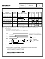
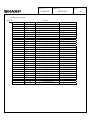
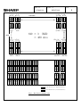
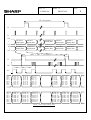
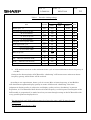
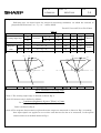
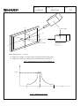
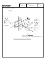
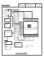
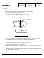
LM10V332
Color STN LCD Module
(Model Number: LM10V332)
Specifications
Spec No.: LC99213A
Dated: May 31. 2002
NOTICE
This publication is the proprietary of SHARP and is copyrighted, with all rights reserved. Under the
copyright laws, no part of this publication may be reproduced or transmitted in any form or by any
means, electronic or mechanical for any purpose, in whole or in part, without the express written
permission of SHARP. Express written permission is also required before any use of this publication
may be made by a third party.
The application circuit examples in this publication are provided to explain the representative
applications of SHARP's devices and are not intended to guarantee any circuit design or permit any
industrial property right or other rights to be executed. SHARP takes no responsibility for any
problems related to any industrial property right or a third party resulting from the use of SHARP's
devices, except for those resulting directly from device manufacturing processes.
In the absence of confirmation by device specification sheets, SHARP takes no responsibility for any
defects that occur in equipment using any of SHARP's devices, shown in catalogs, data books, etc.
Contact SHARP in order to obtain the latest device specification sheets before using any SHARP's
device.
SHARP reserves the right to make changes in the specifications, characteristics, data, materials,
structures and other contents described herein at any time without notice in order to improve design or
reliability. Contact SHARP in order to obtain the latest specification sheets before using any SHARP's
device. Manufacturing locations are also subject to change without notice.
Observe the following points when using any device in this publication. SHARP takes no responsibility
for damage caused by improper use of the devices.
The devices in this publication are designed for use in general electronic equipment designs, such as:
・Automotive auxiliary information display
・Automotive audio visual equipment
The appropriate design measures should be taken to ensure reliability and safety when SHARP's
devices are used for equipment such as:
・Transportation control and safety equipment(i.e., aircraft, trains, automobiles, etc.)
・Traffic signals
・Gas leakage sensor breakers
・Alarm equipment
・Various safety devices etc.
SHARP's devices shall not be used for equipment that requires extremely high level of reliability, such
as:
・Military and space applications
・Nuclear power control equipment
・Medical equipment for life support
Contact a SHARP representative, in advance, when intending to use SHARP's devices for any "specific"
applications other than those recommended by SHARP.
Contact and consult with a SHARP representative if there are any questions about the contents of this
publication.
RECORDS OF REVISION
DATE
JUL.12.1999
REF.PAGE
PARAGRAPH
DRAWING No.
P5,P6
REVISED
SUMMARY
NO.
1
P5 /Table5
P10 /Table7
P16 /Fig7
P21 /Fig11
P25
1
1
Ambient temperature
Supply current, Power comsumption,
Rush current
Data set up time
1
1
1
VDD on/off cycle,
Regulation “d”,”g”,”h”
Applicable inspection standard
DOC.FIRST ISSUE
FEB.17.1999
CHECK
AND
APPROVAL
SPEC No.
MODEL No.
LC99213A
Contents
LM10V332
Page
1.Application
2
2.Construction and Outline
2
3.Mechanical Specifications
3
4.Absolute Maximum Ratings
3
4-1.Electrical absolute maximum ratings
3
4-2.Enviroment Conditions
4
5.Electrical Specifications
5
5-1.Electrical characteristics
5
5-2.Interface signals
6
6.Module Driving Method
12
6-1.Circuit configuration
12
6-2.Display face configuration
12
6-3.Input data and control signal
12
7.Optical Characteristics
14
8.Characteristics of Backlight
19
9.Supply voltage sequence condition
21
10.Cautions
22
11.Applicable inspection standard
25
Warning
25
PAGE
1
SPEC No.
LC99213A
PAGE
MODEL No.
LM10V332
2
1. Application
This data sheet is to introduce the specification of LM10V332, Passive Matrix type Color LCD
module.
2. Construction and Outline
Construction: 640×480 dots color display module consisting of an LCD panel, PWB(printed wiring
board) with electric components mounted onto, TCP(tape carrier package) to connect the LCD panel
and PWB electrically, and plastic chassis with CCFT back light and bezel to fix them mechanically.
Signal ground(Vss) is connected with the metal bezel.
DC/DC converter is built in.
PW B
TCP
L C D panel
B ezel
(w ith A n ti -g la re tre a tm e n t, P e n c il h a rd n e s s 3 H )
P la s tic c h a s s is
Outline
:See Fig. 13
Connection
:See Fig. 13 and Table 6
L ig h t P ip e
CCFT
B ezel
SPEC No.
PAGE
MODEL No.
LC99213A
LM10V332
3. Mechanical Specification
Table1
Parameter
Outline dimensions
Specifications
Unit
264±0.5(W)×193.6±0.5(H)×8.5MAX(D)
Mm
Bezel opening area
215.2±0.3(W)×162.4±0.3(H)
mm
Display format
640(W)×480(H) full dots
mm
Dot size
0.09×RGB(W)×0.31(H)
-
Dot spacing
0.02
mm
Normally black *2
-
Approx. 450
g
*1
Base color
Weight
*1 Due to the characteristics of the LC material, the colors vary with environmental
temperature.
*2 Negative-type display
Display data “H” : ON
Display data “L” : OFF
→ transmission
→ light isolation
4.Absolute Maximum Ratings
4-1.Electrical absolute maximum ratings
Table 2
Parameter
Symbol
MIN.
MAX.
Unit
Remark
Supply voltage(Logic)
VDD-VSS
0
6.0
V
Ta=25 ℃
Input voltage
VIN
-0.3
VDD+0.3
V
Ta=25 ℃
3
SPEC No.
PAGE
MODEL No.
LC99213A
LM10V332
4
4-2.Environment Conditions
Table 3
Tstg
Item
Ambient temperature
Topr
MIN.
MAX.
MIN.
-25 ℃
+60 ℃
0 ℃
Remark
MAX.
1 +50
℃
+40℃
Note 4)
Humidity
Note 1)
Note 1)
No condensation
Vibration
Note 2)
Note 2)
3 directions(X/Y/Z)
Shock
Note 3)
Note 3)
6 directions(±X±Y±Z)
Note 1) Ta≦40 ℃
Ta>40 ℃
95 % RH Max.
Absolute humidity shall be less than Ta=40 ℃/95 % RH.
Note 2)
Table 4
Frequency
10 Hz~57 Hz
57 Hz~500 Hz
Vibration level
-
9.8 m/s2
Vibration width
0.075 mm
-
10 Hz~500 Hz~10 Hz/11.0 min
Interval
2 hours for each direction of X/Y/Z (6 hours as total)
Note 3)
Acceleration
Pulse width
: 490 m/s2
: 11 ms
3 times for each directions of ±X/±Y/±Z
Note 4) As opt-electrical characteristics of LCD will be changed, dependent on the temperature,
the confirmation of display quality and characteristics has to be done after temperature is
set at 25℃ and it becomes stable.
SPEC No.
PAGE
MODEL No.
LC99213A
LM10V332
5
5.Electrical Specifications
5-1. Electrical charasteristics
Table 5
Parameter
Symbol
Supply voltage (Logic)
VDD-VSS
Ta=25 ℃
Conditions
1
VDD= 5.0 V±10 %
Min.
Typ.
Max.
Unit
4.5
5.0
5.5
V
0.8
1.95
2.8
V
0.8VDD
-
VDD
V
-
210
90
1 1050
450
0.2VDD
1 320
135
1 1600
680
1 2A×2
1A×2
1 1A×10
0.5A×20
V
Ta = 0~50 40℃(Note
1)
Contrast adjust voltage
Vcon -VSS
Input signal voltage
VIN
1
Ta = 0~40 ℃
“H” level
1
“L” level
Ta = 0~
50 40℃
0
1
Supply current(Logic)
IDD
Note 2)
-
Power comsumption
Pd
Note 2)
-
IDD
Ta=25℃,Note 1)-①
-
-
Ta=25℃,Note 1)-②
-
-
Rush current(Logic)
mA
mW
ms
μs
Note 1) Under the following conditions.;Logic voltage(VDD) should be designed to supply following
Inrush current.
①Immediately after the rise of VDD .
②Under the situation that DISP signal is on and kept steady.
Measurement Circuit: TMD-18-3
VDD
(VDD Power Supply)(TAKASAGO)
YD etc
A:
DISP
IDD
2A
1AMAX
B: 2 ms MAX
B
A
1
D
C
C:
D:
1
1A
0.5AMAX
1
10 μs
20μs MAX
Note 2) Under the following condetions
Vcon-Vss: contrast max.(1.95V typ.)
VDD-VSS=5V,Frame frequency=120Hz, Display pattern : black/white stripe pattern.
□□□□□□□□□□□□□□□□□□□□
■■■■■■■■■■■■■■■■■■■■
□□□□□□□□□□□□□□□□□□□□
■■■■■■■■■■■■■■■■■■■■
This value Is direct current.
SPEC No.
LC99213A
PAGE
MODEL No.
LM10V332
5-2.Interface signals
LCD
Pin No.
1
2
3
4
5
6
7
8
9
10
11
12
13
14
15
16
17
18
19
20
21
22
23
24
25
26
27
28
29
30
31
Symbol
DL4
VSS
DL5
YD
DL6
LP
DL7
VSS
VSS
XCK
DL0
Vcon
DL1
VDD
VSS
VDD
DL2
DISP
DL3
NC
VSS
DU3
DU4
DU2
DU5
DU1
VSS
DU0
DU6
VSS
DU7
Table 6
Description
Display data signal
Ground potential
Display data signal
Scan start-up signal
Display data signal
Input data latch signal
Display data signal
Ground potential
Ground potential
Data input clock signal
Display data signal
Contrast adjust voltage
Display data signal
Power supply for logic and LCD
Ground potential
Power supply for logic and LCD
Display data signal
Display control signal
Display data signal
Ground potential
Display data signal
Display data signal
Display data signal
Display data signal
Display data signal
Ground potential
Display data signal
Display data signal
Ground potential
Display data signal
Level
H(ON), L(OFF)
H(ON), L(OFF)
“H”
H(ON), L(OFF)
“H” → “L”
H(ON), L(OFF)
“H” → “L”
H(ON), L(OFF)
H(ON), L(OFF)
H(ON), L(OFF)
H(ON), L(OFF)
H(ON), L(OFF)
H(ON), L(OFF)
H(ON), L(OFF)
H(ON), L(OFF)
H(ON), L(OFF)
H(ON), L(OFF)
H(ON), L(OFF)
H(ON), L(OFF)
H(ON), L(OFF)
6
SPEC No.
PAGE
MODEL No.
LC99213A
LM10V332
CCFT
Pin No
Symbol
Description
Level
1
HV
High voltage line (from Inverter)
-
2
NC
NC
-
3
GND
Ground line (from Inverter)
-
LCD
Used connector : DF9B-31P-1V(HIROSE)
Mating connector : DF9B-31S-1V(HIROSE)
CCFT
Used connector
: BHR-03VS-1(JST)
Mating connector : SM02(8.0)B-BHS(JST)
Except above connector shall be out of guaranty.
7
SPEC No.
LC99213A
(1,1)
(1,2)
PAGE
MODEL No.
LM10V332
(1,639) (1,640)
COLUMN
RGB RGB
RGB RGB
RGB RGB
RGB RGB
(2,1)
(2,2)
(2,639) (2,640)
640 × 3 (RGB)
× 480 dots
ROW
(479,1) (479,2)
(479,639) (479,640)
RGB RGB
RGB RGB
RGB RGB
RGB RGB
(480,1) (480,2)
(480,639) (480,640)
RGB
DUDUDU
7 6 5
RGB
DUDUDU
4 3 2
RGB
DUDUDU
1 0 7
RGB
DUDUDU
6 5 4
RGB
DUDUDU
3 2 1
RGB
DUDUDU
5 4 3
RGB
DUDUDU
2 1 0
RGB
DUDUDU
7 6 5
RGB
DUDUDU
4 3 2
RGB
DUDUDU
1 0 7
RGB
DUDUDU
6 5 4
RGB
DUDUDU
3 2 1
RGB
DUDUDU
5 4 3
RGB
DUDUDU
2 1 0
RGB
DLDLDL
7 6 5
RGB
DLDLDL
4 3 2
RGB
DLDLDL
1 0 7
RGB
DLDLDL
6 5 4
RGB
DLDLDL
3 2 1
RGB RGB
DLDLDL DLDLDL
5 4 3 2 1 0
RGB
DLDLDL
7 6 5
RGB
DLDLDL
4 3 2
RGB
DLDLDL
1 0 7
RGB
DLDLDL
6 5 4
RGB
DLDLDL
3 2 1
RGB
DLDLDL
5 4 3
RGB
DLDLDL
2 1 0
Upper SEG Drevers , Upper data(DU0-7)
Lower SEG Drivers , Lower data(DL0-7)
Fig.1
Dot chart of display area
8
SPEC No.
PAGE
MODEL No.
LC99213A
LM10V332
LP×244 pulses
YD
LP
~
DU0
1th line’s
display data
2th line’s
display data
244th line’s
display data
1th line’s
display data
2th line’s
display data
241th line’s
display data
242th line’s
display data
484h line’s
display data
241th line’s
display data
242th line’s
display data
DL7
~
DL0
DL7
XCK × 640 × (3/8) pulses
LP
XCK
XCK
DU7
DU6
DU5
DU4
DU3
DU2
DU1
DU0
R(1,1)
G(1,1)
B(1,1)
R(1,2)
G(1,2)
B(1,2)
R(1,3)
G(1,3)
B(1,3)
R(1,4)
G(1,4)
B(1,4)
R(1,5)
G(1,5)
B(1,5)
R(1,6)
DL7
DL6
DL5
DL4
DL3
DL2
DL1
DL0
R(241,1)
G(241,1)
B(241,1)
R(241,2)
G(241,2)
B(241,2)
R(241,3)
G(241,3)
B(241,3)
R(241,4)
G(241,4)
B(241,4)
R(241,5)
G(241,5)
B(241,5)
R(241,6)
G(1,6)
B(1,6)
R(1,7)
G(1,7)
B(1,7)
R(1,8)
G(1,8)
B(1,8)
R(1,9)
G(1,9)
B(1,9)
R(1,10)
G(1,10)
B(1,10)
R(1,11)
G(1,11)
B(1,11)
R(1,12)
G(1,12)
B(1,12)
R(1,13)
G(1,13)
B(1,13)
R(1,14)
G(1,14)
B(1,14)
R(1,15)
G(1,15)
B(1,15)
R(1,16)
G(1,16)
B(1,16)
G(241,6)
B(241,6)
R(241,7)
G(241,7)
B(241,7)
R(241,8)
G(241,8)
B(241,8)
R(241,9)
G(241,9)
B(241,9)
R(241,10)
G(241,10)
B(241,10)
R(241,11)
G(241,11)
B(241,11)
R(241,12)
G(241,12)
B(241,12)
R(241,13)
G(241,13)
B(241,13)
R(241,14)
G(241,14)
B(241,14)
R(241,15)
G(241,15)
B(241,15)
R(241,16)
G(241,16)
B(241,16)
Fig.2
Data Input timing chart
9
SPEC No.
LC99213A
Table 7
Item
PAGE
MODEL No.
LM10V332
Interface timing ratings
Symbol
Rating
MIN.
TYP.
MAX.
tFRM
8.33
YD signal “H” level set up time
tHYS
100
ns
“H” level hold time
tHYH
100
ns
“L” level set up time
tLYS
100
ns
“L” level hold time
tLYH
40
ns
tWLPH
200
ns
tCK
80
ns
“H” level clock width
tWCKH
30
ns
“L” level clock width
tWCKL
30
5
15
ns
XCK signal clock cycle
16.94
Unit
Frame cycle *1
LP signal “H” level pulse width
1
ms
Data set up time
tDS
hold time
tDH
40
ns
LP↑ allowance time from XCK↓
tLS
200
ns
XCK↑ allowance time from LP↓
tLH
200
ns
Input signal rise/fall time *1
tr,tf
*1
10
ns
12
ns
LCD module functions at the minimum frame cycle of 8.33 ms(Maximum frame frequency of
120 Hz).
Owing to the characteristics of LCD module, “shadowing” will become more eminent as frame
frequency goesup, while flicker will be reduced.
According to our experiments, frame cycle of 8.33 ms Min. or frame frequency of 120 Hz Max.
will demonstrate optimum display quality in terms of flicker and “shadowing”. But since
judgment of display quality is subjective and display quality such as “shadowing” is pattern
dependent, it is recommended that decision of frame frequency, to which power consumption of the
LCD module is proportional, be made based on your own through testing on the LCD module with
every possible patterns displayed on it.
The intervals of one LP fall and next must be always the same, and LPs must be input
continuously.
The intervals must be 70μs Max.
SPEC No.
PAGE
MODEL No.
LC99213A
LM10V332
t FRM
t HYH
t HYS
t
t
LYS
LYH
YD
t WLPH
LP
LP
t CK
tr
t LS
XCK
tf
tW C K H
tW C K L
t LH
t DH
t DS
D U 0~ 7
D L 0~ 7
V IH = 0 .8 V D D
V IL = 0 .2 V D D
F ig .3 In te rfa c e tim in g c h a rt
11
SPEC No.
MODEL No.
LC99213A
PAGE
LM10V332
12
6. Module Driving Method
6-1. Circuit configuration
Fig.9 shows the block diagram of the module’s circuitry.
6-2. Display face configuration
The display consists of 640×3(R,G,B)×480 dots as shown in Fig. 1.
The interface is single panel with double drive to be driven at 1/240(1/244) duty ratio.
(1/240:an odd number frame, 1/244:an even number frame)
6-3. Input data and control signal
The LCD driver is 240 bits LSI, consisting of shift registers, latch circuits and LCD driver
circuits. Input data for each row (640×3 R,G,B) will be sequentially transferred in the
form of 8 bit parallel data through shift registers from top left of the display together with
clock signal (XCK).
When input of one row (640×3 R,G,B) is completed, the data will be latched in the form of
parallel data corresponding to the signal electrodes by the falling edge of latch signal (LP)
then,the corresponding drive signals will be transmitted to the 640×3 lines of column
electrodes of the LCD panel by the LCD drive circuits.
At this time, scan start-up signal (YD) has been transferred from the scan signal driver to
the 1st row of scan electrodes, and the contents of the data signals are displayed on the 1st
row of the display face according to the combinations of voltages applied to the scan and
signal electrodes of the LCD. While the data of 1st row are being displayed, the data of 2nd
row are entered. When data for 640×3 dots have been transferred, they will be latched by
the falling edge of LP, switching the display to the 2nd row.
Such data input will be repeated up to the 240(244)th row of each display segment, from
upper row to lower rows, to complete one frame of display by time sharing method.
Simultaneously the same scanning sequence occur at the lower panel.
Then data input proceeds to the next display frame.
YD generates scan signal to drive horizontal electrodes.
Since DC voltage, if applied to LCD panel, causes chemical reaction in LC materials,
causing deterioration of the materials, drive wave-form shall be inverted at every display
frame to prevent the generation of such DC voltage. Control signal M plays such a role.
SPEC No.
MODEL No.
LC99213A
PAGE
LM10V332
13
Because of the characteristics of CMOS driver LSI, the power consumption of the display
module goes up with the clock frequency of XCK.
To minimize data transfer speed of XCK clock the LSI has the system of transferring 8 bit
parallel data through the 8 lines of shift registers.
Thanks to this system the power consumption of the display module is minimized.
In this circuit configuration, 8 bit display data shall input to data input pins of DU0-7 and
DL0-7.
Furthermore, the display module has bus line system for data input to minimize the power
consumption with data input terminals of each driver LSI being activated only when
relevant data input is fed.
Data input for column electrodes and chip select of driver LSI are made as follows:
The driver LSI at the left end of the display face is first selected, and the adjacent driver
LSI right next side is selected when data of 240 dot (30XCK) is fed. This process is
sequentially continued until data is fed to the driver LSI at the right end of the display
face. This process is followed simultaneously both at the top and bottom column drivers
LSI’s.
Thus data input will be made through 8 bit bus line sequentially from the left end of the
display face.
Since this display module contains no refresh RAM, it requires the above data and timing
pulse inputs even for static display.
The timing chart of input signals are shown in fig. 3 and Table 7.
SPEC No.
PAGE
MODEL No.
LC99213A
LM10V332
14
7. Optical Characteristics
Following spec are based upon the electrical measuring conditions, on which the contrast of
perpendicular direction(θx = θy = 0°) will be MAX..
Ta=25℃,VDD=5.0V,VCON-VSS=Vmax
Table 8
Parameter
Symbol
Condition
θx
Viewing angle range
Co>5.0
θy
Contrast ratio
MIN.
TYP.
MAX.
Unit
θy = 0 °
-30
-
30
deg.
θx = 0 °
-15
-
25
deg.
Co
θx =θy = 0 °
35
50
-
-
Response
Rise
τr
θx =θy = 0 °
-
220
300
ms
time
Decay
τd
θx =θy = 0 °
-
80
100
ms
x
θx =θy = 0 °
-
0.275
-
-
+θ y
Remark
Note 1)
Note2)
Note3)
+θ y
+θ y
-θ x
+θ x
-θ y
+θ x
-θ x
+θ x
-θ x
-θ y
y
-θ y
θx =θy = 0 °
Fig.4
-
0.320
-
-
Definition of Viewing Angle
Note 1) The viewing angle range is defined as shown Fig.4.
Note 2) Contrast ratio is defined as follows:
Co =
Luminance(brightness) all pixes "White" at Vmax
Luminance(brightness) all pixes "dark " at Vmax
Vmax is defined in Fig.6.
Note 3) The response characteristics of photo-detector output are measured as shown in Fig.7, assuming
that input signals are applied so as to select and deselect the dot to be measured, in the optical
characteristics test method shown in Fig.5.
SPEC No.
PAGE
MODEL No.
LC99213A
LM10V332
+θy
15
TOPCON BM-7
+θy
-θx
-θx
normal
Measuring
Field: 2 ゚
+θx
-θy
Measuring Spot Size : φ10 mm
θx : Angle from “normal” to viewing surface rotated about the horizontal axis.
θy : Angle from “normal” to viewing surface rotated about the vertical axis.
Fig.5
Optical Characteristics Test Method Ⅰ
Comax.
Vmax.
Fig.6
Definition of Vmax
Vcon-Vss (V)
SPEC No.
PAGE
MODEL No.
LC99213A
LM10V332
16
(Response Measurement)
Ta = 25 ℃
In dark room
θy(+)
1
85mm
350mm
Computer
LCD Control
θx(-)
circuit
LCD Module
A/D
θx(+)
Converter
normal
θy(-)
θx=θy= 0°
1
TOPCON BM7 + quartz fiber
(Measuring spot size :φ10 mm, Measuring Field : 2°)
Fig. 7
Optical Characteristics Test Method Ⅱ
SPEC No.
LC99213A
PAGE
MODEL No.
LM10V332
17
[Drive waveform]
Driving voltage
1/244 Duty Ratio
Non-select
waveform
Select waveform
Non-select
waveform
10 %
90 %
100 %
Photo detector output
[Responce waveform]
τr
τd
Fig.8
Definition of Response time
τr :
Rise time
τd :
Decay time
SPEC No.
LC99213A
Resister
DU0-DU7
DL0-DL7
XCK
LP
LM10V332
Chip inductor
Buffer I.C
YD
PAGE
MODEL No.
DISP
SEG Drivers (Upper)
M general
circuit
(1,1)(1,2)
(2,1)(2,2)
COM Drivers
Sequence
control
circuit
DISP
(1,640)
(2,640)
RGB
(240,1)
(241,1)
(240,640)
(241,640)
640 X RGB X480 DOTS LCD
Bias generator
&
Protection circuit
(480,1)
(480,640)
SEG Drivers (Lower)
V SS
V DD
DC/DC
Converter
Vcon
Tempareture
Compensation
Circuit
CCFT
Inverter
Fig. 9 Circuit block diagram
CCFT
18
SPEC No.
PAGE
MODEL No.
LC99213A
LM10V332
19
8.Characteristics of Backlight
The ratings are given on condition that the following conditions are satisfied.
1) Rating(Note)
Parameter
MIN.
TYP.
MAX.
Unit
Brightness
120
160
-
cd/m2
2) Measurement circuit : CXA-M10L(TDK) (at IL = 5.5 mArms)
3) Measurement equipment :
BM-7 (TOPCON Corporation)
4) Measurement conditions
4-1. Measurement circuit voltage : DC = 10.6 V, at primary side
4-2.
LCD: All digits WHITE, VDD= 5 V, Vcon-VSS = Vmax,
DU0-7=“H”(White), DL0-7=“H”(White)
4-3. Ambient temperature : 25 ℃
Measurement shall be executed 30 minutes after turning on.
5)
Used lamp : K-CE235-24-50BH(WEST ELECTRIC CO.,LTD.) : 1 pc
5-1) Rating (1pc)
Parameter
Symbol
MIN.
TYP.
MAX.
Unit
Remark
Lamp voltage
VL
-
520
-
Vrms
-
Lamp current
IL
-
5.5
-
mAr
(*1)
ms
Lamp power consumption
PL
-
2.86
-
W
(*2)
Lamp frequency
FL
30
-
70
kHz
-
Kick-off voltage
VS
-
-
760
Vrms
Ta=25 ℃
-
-
1300
Vrms
Ta= 0 ℃(*3)
LL
25 000
40 000
-
h
Ta=25 ℃(*4)
LL
1 000
-
-
h
Ta=0 ℃(*4)
Lamp life time
Within no conductor closed. (CCFT only)
*1 It is recommended that IL be not more than 5.5mArms so that heat radiation of CCFT
backlight may least affect the display quality.
*2
Power consumption excluded inverter loss.
*3
The circuit voltage(VS) of the inverter should be designed to have some margin, because VS
may be increased due to the leak current in case of the LCD module.
*4
Average life time of CCFT will be decreased when LCD is operating at lower temperature.
SPEC No.
PAGE
MODEL No.
LC99213A
LM10V332
20
5-2) Operating life
The operating life time is 25 000 hours or more at 5.5 mA , at 25℃.
(Operating life with CXA-M10L or equivalent.)
The inverter should meet the following conditions to keep the specified life time of used lamp;
Since, symmetric waveform without spike in positive and negative
Output frequency range : 30 kHz-70 kHz
Make sure the operating conditions by executing the burn-in enough time.
The operating life time is defined as having ended when any of the following conditions occur;
25± 1 ℃
When the voltage required for initial discharge has reached 110 % of the initials value.
When the illuminence quantity of light has decreased to 50 % of the initials value.
(NOTE) Rating are defined as the average brightness inside the viewing area specified in Fig.10.
ACTIVE AREA
②
120
③
①
240
⑤
360
④
dot
160
320
Fig.10
480
dot
Measuring points (①-⑤)
SPEC No.
PAGE
MODEL No.
LC99213A
LM10V332
21
9. Supply voltage sequence condition
1
500
1500ms MIN. (NOTE 1)
a (NOTE 2)
e
VDD
YD
Interface timing active operation
LP
XCK
c (NOTE 3)
1
h
f
DATA
DISP
b
1
1
4.5 V
3V
1
3.0V
3.5 V
1
2.0V
2.0V
3V
1.0V
VDD
VSS
d
g
Fig.11
Supply voltage sequence condition
POWER ON
Symbol
POWER OFF
Allowable value
Symbol
a
0 ms MIN.
1 s MAX.
e
b
-
100 ns MAX.
f
c
50 ms MIN.
-
d
-
10 ms MAX.
1
0 ms MIN.
1 s MAX.
0 ms MIN.
10 ms MIN.
1 ms MIN.
1 s MAX.
1
g
Allowable value
h
1s MIN.
-
-
(NOTE 1) Power ON/OFF cycle time. All signals and power line shall be in accordance with above
sequence in case of power ON/OFF.
(NOTE 2) In this period, YD and LP shall be “L” level.
(NOTE 3) Before DISP rise up, the signals of YD,LP,XCK,DATA must be input, and the above
condition of “a” must be satisfied. The signals which comply with the interface timing in
Fig.2,Fig.3, and table 7, must be input.
SPEC No.
MODEL No.
LC99213A
LM10V332
PAGE
22
10. Cautions
1)
Industrial(Mechanical) design of the product in which this LCD module will be incorporated must
be made so that the viewing angle characteristics of the LCD may be optimized.
This module’s viewing angle is illustrated in Fig.12.
θy MIN. < viewing angle <θy MAX.
(For the specific values ofθy MIN., andθy MAX., refer to the table8)
Please consider the optimum viewing conditions according to the purpose when installing the
module.
Viewing direction +θy
θy=0 °(Normal line)
-θy
Panel surface
Fig.12 Definition of viewing angle
2)
This module should be installed using mounting holes of metal bezel. When installing the
module,pay attention and handle carefully not to allow any undue stress such as twist or bend.
3)
Since the front polarizer is easily damaged. Please pay attention not to scratch on its face.
It is recommended to use a transparent acrylic resin board or other type of protective panel on
the surface of the LCD module to protect the polarizer, LCD panel, etc..
4)
If the surface of the LCD panel is required to be cleaned, wipe it swiftly with cotton or other soft
cloth. If it is not still clear completely, blow on and wipe it.
5)
Water droplets, etc. must be wiped off immediately since they may cause color changes, staining,
etc., if it remained for a long time.
6)
Since LCD is made of glass substrate, dropping the module or banging it against hard objects
may cause cracking or fragmentation.
7)
Since CMOS LSIs are equipped in this module, following countermeasures must be taken to
avoid electrostatics charge.
SPEC No.
LC99213A
MODEL No.
PAGE
LM10V332
23
1. Operator
Electrostatic shielding clothes shall be had because it is feared that the static electricity is
electrified to human body in case that operator have a insulating garment.
2. Equipment
There is a possibility that the static electricity is charged to equipment which have a function of
peeling or mechanism of friction(EX: Conveyer, soldering iron, working table), so the
countermeasure (electrostatic earth:1×10⁸Ω) should be made.
3. Floor
Floor is a important part to leak static electricity which is generated from human body or
equipment.There is a possibility that the static electricity is charged to them without leakage
in case of insulating floor,so the countermeasure(electrostatic earth:1×10⁸Ω) should be made.
4.Humidity
Humidity of working room may lower electrostatics generating material’s resistance and have
something to prevent electrifying. So, humidity should be kept over 50% because humidity less
than 50 % may
increase material’s electrostatic earth resistance and it become easy to electrify.
5. Transportation/storage
The measure should be made for storage materials because there is a possibility that the static
electricity,which electrify to human body or storage materials like container by friction or
peeling,cause the dielectric charge.
6. Others
The laminator is attached on the surface of LCD module to prevent from scratches, fouling and
dust. It should be peeled off unhurriedly with using static eliminator.
And also, static eliminator should be installed to prevent LCD module from electrifying at
assembling line.
8)
Don’t use any materials which emit gas from epoxy resin(amines’ hardener) and silicon
adhesive agent(dealcohol or deoxym) to prevent change polarizer color owing to gas.
9)
Since leakage current, which may be caused by routing of CCFT cables, etc., may affect the
brightness of display, the inverter has to be designed taking the leakage current into
consideration. Thorough evaluation of the LCD module/inverter built into its host equipment
shall be conducted, therefore, to ensure the specified brightness.
10) Avoid to expose the module to the direct sun-light, strong ultraviolet light, etc. for a long time.
11) If stored at temperatures under specified storage temperature, the LC may freeze and be
deteriorated. If storage temperature exceed the specified rating, the molecular orientation of
the LC may change to that of a liquid, and they may not revert to their original state. Therefore,
the module should be always stored at normal room temperature.
12) Disassembling the LCD module can cause permanent damage and should be strictly avoided.
SPEC No.
MODEL No.
LC99213A
PAGE
LM10V332
24
13) Procedure insert mating connector
When the mating connector is inserted, it should be parallel to the used connector of LCD
module and it should be inserted on horizontal firm base.
When the mating connector is attempted to be fixed to LCD connector, it should be inserted
properly in order not to create a gap as shown following diagram 2).
Please insert the connector as both edge is placed to the connect position of LCD connector.
1)Method of correct insert
Stress is dispersed
Base (horizontal film base) is required
2) Method of wrong insert
Stress is not dispersed
Base (horizontal film base) is required
SPEC No.
MODEL No.
LC99213A
14) This
specification
PAGE
LM10V332
25
describes
display quality in case of no gray scale. Since display quality can be
affected by gray scale methods, display quality shall be carefully evaluated for the usability of
LCD module in case gray scale is displayed on the LCD module.
15) The module should be driven according to the specified ratings to avoid permanent damage.
DC voltage drive leads to rapid deterioration of LC, so ensure that the drive is alternating
waveform by continuous application of the signal M. Especially the power ON/OFF sequence
shown on Page 21 should be kept to avoid latch-up of drive LSI and application of DC voltage to
LCD panel
16) It is a characteristic of LCD to maintain the displaying pattern when the pattern is applied for a
long time.(Image retention)
To prevent image retention, please do not apply the fixed pattern for along time by pre-installing
such programs at your side.
17) This phenomenon (image retention) is not deterioration of LCD. If it happens, you can remove it
by applying different patterns.
18) CCFT backlight should be kept OFF during VDD is “L” level.
11. Applicable inspection standard
The LCD module shall meet the following inspection standard :
1
S-U-014 S-U-035
WARNING
Don’t use any materials which emit following gas from epoxy resin (amines’ hardener) and
silicone adhesive agent (dealcohol or deoxym) to prevent change polarizer color owing to gas.
SPECIFICATIONS ARE SUBJECT TO CHANGE WITHOUT NOTICE.
Suggested applications (if any) are for standard use; See Important Restrictions for limitations on special applications. See Limited
Warranty for SHARP’s product warranty. The Limited Warranty is in lieu, and exclusive of, all other warranties, express or implied.
ALL EXPRESS AND IMPLIED WARRANTIES, INCLUDING THE WARRANTIES OF MERCHANTABILITY, FITNESS FOR USE AND
FITNESS FOR A PARTICULAR PURPOSE, ARE SPECIFICALLY EXCLUDED. In no event will SHARP be liable, or in any way responsible,
for any incidental or consequential economic or property damage.
NORTH AMERICA
EUROPE
JAPAN
SHARP Microelectronics of the Americas
5700 NW Pacific Rim Blvd.
Camas, WA 98607, U.S.A.
Phone: (1) 360-834-2500
Fax: (1) 360-834-8903
Fast Info: (1) 800-833-9437
www.sharpsma.com
SHARP Microelectronics Europe
Division of Sharp Electronics (Europe) GmbH
Sonninstrasse 3
20097 Hamburg, Germany
Phone: (49) 40-2376-2286
Fax: (49) 40-2376-2232
www.sharpsme.com
SHARP Corporation
Electronic Components & Devices
22-22 Nagaike-cho, Abeno-Ku
Osaka 545-8522, Japan
Phone: (81) 6-6621-1221
Fax: (81) 6117-725300/6117-725301
www.sharp-world.com
TAIWAN
SINGAPORE
KOREA
SHARP Electronic Components
(Taiwan) Corporation
8F-A, No. 16, Sec. 4, Nanking E. Rd.
Taipei, Taiwan, Republic of China
Phone: (886) 2-2577-7341
Fax: (886) 2-2577-7326/2-2577-7328
SHARP Electronics (Singapore) PTE., Ltd.
438A, Alexandra Road, #05-01/02
Alexandra Technopark,
Singapore 119967
Phone: (65) 271-3566
Fax: (65) 271-3855
SHARP Electronic Components
(Korea) Corporation
RM 501 Geosung B/D, 541
Dohwa-dong, Mapo-ku
Seoul 121-701, Korea
Phone: (82) 2-711-5813 ~ 8
Fax: (82) 2-711-5819
CHINA
HONG KONG
SHARP Microelectronics of China
(Shanghai) Co., Ltd.
28 Xin Jin Qiao Road King Tower 16F
Pudong Shanghai, 201206 P.R. China
Phone: (86) 21-5854-7710/21-5834-6056
Fax: (86) 21-5854-4340/21-5834-6057
Head Office:
No. 360, Bashen Road,
Xin Development Bldg. 22
Waigaoqiao Free Trade Zone Shanghai
200131 P.R. China
Email: [email protected]
SHARP-ROXY (Hong Kong) Ltd.
3rd Business Division,
17/F, Admiralty Centre, Tower 1
18 Harcourt Road, Hong Kong
Phone: (852) 28229311
Fax: (852) 28660779
www.sharp.com.hk
Shenzhen Representative Office:
Room 13B1, Tower C,
Electronics Science & Technology Building
Shen Nan Zhong Road
Shenzhen, P.R. China
Phone: (86) 755-3273731
Fax: (86) 755-3273735