1
SERVICE MANUAL
(without price)
ELECTRONIC CASH REGISTER
CE-7000
(EX-475B*,C*,D*)
FEB. 2000
Printer Model : M-U420-071
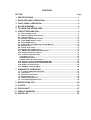
INDEX
CONTENTS
CE-7000
Page
1. SPECIFICATIONS........................................................................................ 1
2. INITIALIZE (MAC) OPERATION .................................................................. 4
3. F-INIT (FMAC) OPERATION ....................................................................... 4
4. BLOCK DIAGRAM ....................................................................................... 5
5. TO OPEN THE UPPER CASE ..................................................................... 7
6. CIRCUIT EXPLANATION ............................................................................ 9
6-1. Power supply circuit .................................................................................................. 9
6-2. Reset and power down circuit ................................................................................. 10
6-3. CPU description ........................................................................................................ 11
6-4. Momory chip selection circuit ................................................................................. 13
6-5. Flash ROM1 address circuit .................................................................................... 14
6-6. Flash ROM2 circuit ................................................................................................... 14
6-7. Flash Pack circuit (Memory Cassette RAC-9) ........................................................ 15
6-8. Memory map ............................................................................................................. 16
6-9. Printer drive circuit ................................................................................................... 17
6-10. RS232C port COM1 circuit ...................................................................................... 17
6-11. RS232C port COM2 and COM3 circuit ................................................................... 18
6-12. Keyboard selection switch ..................................................................................... 19
6-13. To mount optional circuit ....................................................................................... 19
1) Clerk key circuit ........................................................................................................ 19
2) Multi-drawer circuit .................................................................................................. 21
3) Paper near end sensor circuit ................................................................................. 22
6-14. Display controller uPD78015FGC526-AB8 ............................................................ 23
6-15. Segment display driver uPD16312GB-3B4 ............................................................ 24
6-16. DC/DC convertor circuit .......................................................................................... 25
6-17. ARCNET circuit (IO-PB14) ...................................................................................... 25
7. DIAGNOSTIC OPERATION ....................................................................... 31
7-1.
7-2.
7-3.
7-4.
7-5.
7-6.
To start the diagnostic program .............................................................................
Check item ................................................................................................................
Operation of each test ..............................................................................................
Switch status test .....................................................................................................
Individual function test ............................................................................................
To exit the diagnostic mode ....................................................................................
31
31
31
32
33
49
8. ERROR CODE LIST................................................................................... 50
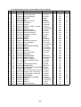
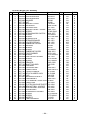
9. IC DATA ..................................................................................................... 53
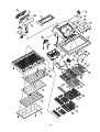
10. PCB LAYOUT ............................................................................................ 67
11. CIRCUIT DIAGRAM ................................................................................... 69
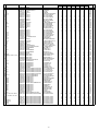
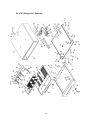
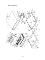
12. PARTS LIST ............................................................................................... 92
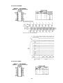
1. SPECIFICATIONS
1-1. Electrical specifications
120V
0.7 A
0.3 A
0.3 A
Max.
Min.
Power OFF
220V
0.4A
0.2A
0.2A
230V
0.4A
0.2A
0.2A
240V
0.4A
0.2A
0.2A
• Power consumption
In operation
• Memory protection
Back-up battery
Back-up period
Battery life
Recharge time
VL3032/1F2
90 days (25 °C)
Replace the battery every 5 years.
48 hours
• Clock & Calendar
Accuracy
Auto calendar
Within ± 30 sec. per month (25 °C)
Effective until 2099 A.D.
1-2. Environmental specifications
• Operating temperature
0 °C ~ 40 °C
• Operating humidity
10 % ~ 90 %
• Storage temperature
-25 °C ~ 65 °C
• Storage humidity
10 % ~ 95 %
• Vibration strength
1.5 G (The machine must be in the carton box)
1-3. Main components
• CPU
Name
Number of control bit
uPD784215GC084-8EU
8bit
Internal RAM
4 KBytes
• RAM1 and 2
Name
Capacity
HY628100ALLG-70
128 K bytes
• Option RAM3 and 4
Name
Capacity
HM628512ALP-7
512 Kbytes
• Flash ROM1
Name
Capacity
LH28F016SCT-L85
2 M bytes
• Flash ROM2
Name
Capacity
LH28F004SCT-L85
512 K bytes
• Display driver
Name
uPD78015FGC-526-AB8
• Printer
Name
Print method
Paper cut
M-U420-071
Impact dot matrix printer
Auto-paper cut
• Roll paper
Type
Size
Roll diam
Thickness
Fine-quality paper
Width 44.5 ± 0.5 mm
83 mm or less
75 ± 15 µm
-1-
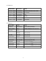
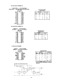
1-4. Drawer List
DRAWER NAME
Specification
NOTE
• DL-2766 (M type)
D-9BC-B84M-9*
EUROPE, Saudi-Arabia, Other countries
• DL-2767 (M type)
D-9BC-B84SM-9*
UK, Germany
• DL-2417 (M type)
D-9BC-B55S-9*
USA
• DL-2517 (M type)
D-9BC-B64S-9*
Canada
• DL-3616 (L type)
D-11BH-B65SS-9*
USA, Canada
• DL-3617 (L type)
D-11BH-B65-9*
Saudi-Arabia
DEVICE NAME
MODEL
NOTE
• RAM CHIP
RAM-610-10LL
Capacity 4Mbits (512 Kbytes)
• Momry Cassette
RAC-9
16Mbits (2 Mbytes) With write protection switch
• Wet cover
WT-77
• Modem
Sports star
56.4Kbps
Recommend model : U.S.Robotics
Com 1 port only
• P/C cable
PRL-CB-2
Com 1 port only
• Handy scanner
HHS-15
Com 2 port only
• Fixed scanner
HS1250
Com 2 port only (PSC model)
• Laser scanner
Quic Scan 6000
Com 2 port only (PSC model)
• Slip printer
SP-1300
Connect to Com 2 or 3.
• Kitchen printer
UP-350
Connect to Com 1,2 or 3.
• Kitchen printer
UP-250
Connect to Com 1,2 or 3.
• Scale
Model 6710
Com 3 only (NCI model)
1-5. Option List
It is possible to drive only one printer.
It is possible to drive until 2 printers.
It is possible to drive until 2 printers.
-2-
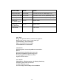
DEVICE NAME
MODEL
NOTE
• Slip printer cable
PRT-CB-8C
Connect Com 2 or 3. (Cable lngth 1.5m)
• External printer cable PRT-CB-8A
Connect to Com 1,2 or 3. (Cable length 3 m)
• External printer cable PRT-CB-8B
Connect to Com 1,2 or 3. (Cable length 5 m)
• Power unit
for External printer
PS-170
Epson model
• Power cord
for power unit
AC-170
Epson model
• Power-board
JDC model
CAUTION
Danger of explosion if battery is incorrectly replaced.
Replace only with the same or equivalent type
recommended by the manufacturer.
Dispose of used batteries according
to the manufacture’s instructions.
VORSICHT !
Explosionsgefahr bei unsachgemäßem Austausch der
Batterie.
Ersatz nur durch denselben oder einen vom
Hersteller empfohlenen gleichwertigen Typ.
Entsorgung gebrauchter Batterien nach
Angaben des Herstellers.
ADVARSEL !
Lithiumbatteri - Eksplosionsfare ved fejlagtig hándtering.
Udskiftning má kun ske med batteri
af samme fabrikat og type.
Levér det brugte batteri tilbage til leverandØren.
-3-
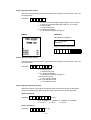
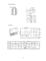
2. INITIALIZE (MAC) OPERATION (CE-7000)
1. Plug the power cord into an AC outlet.
2. Set the mode switch to "OFF" position.
3. While pressing the Journal feed Button, turn the mode switch to "PGM" position.
4. Release the Journal feed button.
5. Input the MAC CODE 1. (11 digits)
6. Press "#2" key. (Wait until beep twice.)
7. Input the MAC CODE 2. (3 digits)
8. Press "#2" key. (Initialization receipt is issued.)
9. Initialize operation is executed.
MAC CODE 1 : D11 to D1 (11 digits)
Description
Choice
Program code
Print PGM mode password, when flag clear
Yes = 0
No = 4
Significant
number 4 digits
Significant
number
Significant
number
D11 =
Fixed
Significant
number A
Significant
number B
No = 0
Yes = 1
D3 D4 =
D2 = A + B
Description
Choice
Program code
Inline baud rate
156Kbps = 0
312Kbps = 1
Significant
number 2 digits
D3 =
Password in PGM3 to 7 mode
Messages and descriptions are written in
English=0, French=1, Spanish=2, German=4
Model for
USA or Canada=2, German=4,
Other area (0.00) =1, Other area (0) = 3
Department No. (15 ,20, or 30)
Use clerk switch or push switch = 0
Use clerk lock Key or secrec code key = 1
For scanning initialization pattern = 0
For check tracking initialization pattern = 2
Use Euro only
D10 to D7 =
D6 =
D5 =
D1 =
MAC CODE 2 : D3 to D1 (3 digits)
Inline physical I.D. number (01 to 32)
D2 to D1 =
3. F-INIT (FMAC) OPERATION
1. Plug the power cord into an AC outlet.
2. Set the mode switch to "OFF" position.
3. While pressing the Receipt feed button , turn the mode switch to "PGM" position.
4. Release the receipt feed button.
5. Press "#2" key.
Note : The location of "#2" key, see "HARD KEY CODE TABLE" on page 31.
—4—
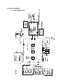
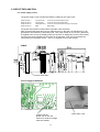
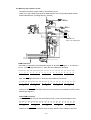
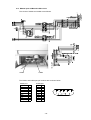
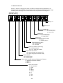
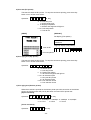
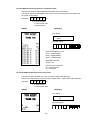
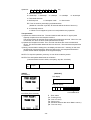
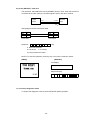
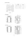
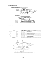
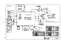
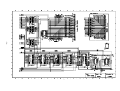
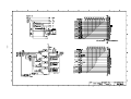
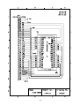
4. BLOCK DIAGRAM
4-1. PCB CONNECTION
-5-
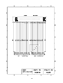
4-2. BLOCK DIAGRAM (CE-7000)
Main display
(Dot & segment)
COM3
COM2
Driver
COM1
Driver
Printer
M-U420-071
Main display
(Dot & segment)
Customer
display
Segment driver
uPD16312GB-3B4
Keyboard
Display controller
uPD78015FGC526-AB8
ARCNET
driver
IN-Line
Printer driver
Display driver and Key control circuit
Address bus A8 - A19
A0 -A7
CPU
uPD784215GC-084-8EU
Address
Latch
I/O selector
Data buffer
Data bus D0 -D7
RAM1
HY628100A
LLG-70
(128 K bytes)
RAM3
(Option)
Flash ROM 1
HM628512ALP-7
512 K bytes
(2 M bytes)
LH28F016SCT-L95
(RAM-610)
Flash ROM 2
LH28F004SCT-L95
(512 K bytes)
RAM2
HY628100A
LLG-70
(128 K bytes)
RAM4
(Option)
HM628512ALP-7
512 K bytes
(RAM-610)
MAIN PCB E457-1 C
Flash pack (Option)
Memory cassette RAC-9
-6-
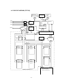
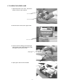
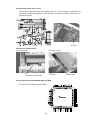
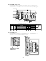
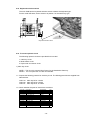
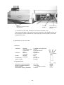
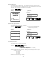
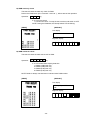
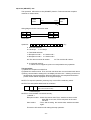
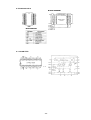
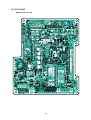
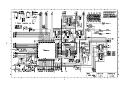
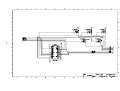
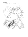
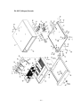
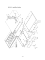
5. TO OPEN THE UPPER CASE
1. Open the printer cover. Then, remove the
ribbon cover from the machine.
Open the printer cover.
Remove the ribbon cover.
2. Remove the 2 screws of the upper case.
Remove the 2 screws.
3. Push the 3 dots marking point at the right
side of lower case. At the same time, slide
the upper case to the front side.
Slide the upper case
to the front side.
Press the 3 dots marking point.
4. Open upper case from the left side.
-7-
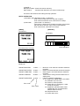
Power switch cover
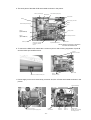
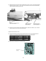
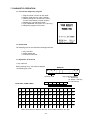
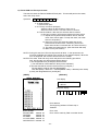
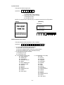
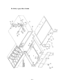
5. The each parts of the Main PCB are located as shown in the picture.
RAM 1 (128 K bytes)
Reset Switch
Flash ROM 1 (2 M bytes)
Printer cable
Battery
Power supply connector
Buzzer
Flash ROM 2 (512 K bytes)
CPU
RAM 4
(Option RAM-610)
Display cable
Clerk key connector
RAM 3
(Option RAM-610)
COM 1 port
Flash pack connector
for Memory cassette
RAC-9
Keyboard select switch
Main PCB
NOTE: RAM2 (128 K bytes) is located on
the back side of Main PCB.
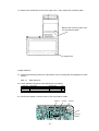
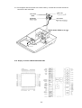
6. To remove the Main PCB, release the 2 screws of point A and 2 locking supporters of point B
and the COM1 port outside screws.
Point B
Remove 2 screws.
Main PCB
Point A
Remove 2 screws.
Remove 2 screws for COM 1 port.
7. Power supply unit cover is removed by 3 screws. And, the 3 Fuses are located as shown in the
picture.
Power transformer
Fuse F3
250V 400mA
Remove the 3 screws.
Then, remove the power supply cover.
-8-
Fuse F2
250V 2A
Fuse F1
250V 1A
Voltage selector
Normally, Do not change
the Voltage position.
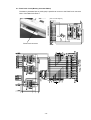
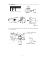
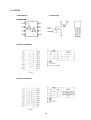
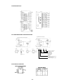
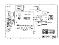
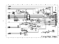
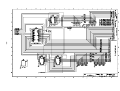
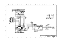
6.CIRCUIT EXPLANATION
6-1. Power supply circuit
The power supply circuit provides the following voltage for the main circuit.
Output Pin No1----Output Pin No.2---Output Pin No.3---Output Pin No.4----
VC1 (DC32.3V):
VC2 (DC24V):
VLED (DC5.85V):
GND:
To the VC line for the Display power.
To the Vp line for the printer power.
To the Vcc,Vcc2 and Vdd for the logic circuit power.
Signal GND.
The power switch SW1 is located at the right side of the lowercase.
After connected the power plug into AC outlet and turn on the SW1, the transformer T1 will
genarate the about AC33V to secondary side. Then, after rectifier circut, the VC1 (DC32.3V)
is supplied to the VC line for display power (for the drive of display tube. Not for LED model.)
The IC2 is the shunt regulator for the control of Q1 transistor. This circuit is genarate the
VC2 (DC24V) for the printer power. The IC1 is regulator for 5V power supply.
Power switch SW1
Power supply PCB E445-S1
Voltage selector
NOTE: Do not turn the
selector to avoid the voltage
selection mistake.
-9-
Power SW1 cover
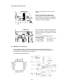
6-2. Reset and power down circuit
The rest and power down circuit are as following circuit. The reset switch is provided for the
hard reset to cleare the system error. Use this switch only when the FMAC or MAC are not
possible to perform.
Reset switch
The position of Reset switch
From top of view
From rear of view
Printer
The mark of reset switch
6-3. CPU pin description(uPD784215GC-084-8EU)
The CPU pin descriptions are as follows:
- 10 -
Reset switch
CPU pin description(uPD784215GC-084-8EU)
Pin No.
1
2
3
4
5
6
7
8
9
10
11
12
13
14
15
16
17
18
19
20
21
22
23
24
25
26
27
28
29
30
31
32
33
34
35
36
37
38
39
40
41
42
43
44
45
46
47
48
49
50
Signal Name
P120
P121
P122
P123
P124
P125
P126
P127
VDD
X2
X1
VSS
XT2
XT1
RESET
P00
P01
P02
P03
P04
P05
P06
AVDD
AVREF0
P10
P11
P12
P13
P14
P15
P16
P17
AVSS
P130
P131
AVREF1
P70
P71
P72
P20
P21
P22
P23
P24
P25
P26
P27
P80
P81
P82
HD1
HD2
HD3
HD4
HD5
HD6
HD7
HDGATE2
VDD
X2
X1
GND
XT2
XT1
RESET
TP
COM2 SEL
CUTTER RP
PWD
VFD BUSY
RP
IRQ ARCNET
VDD
AVREF0
AVREF
HDTH
CROM IN
DWS
DSR1
CI1
CD1
P.N.E.
GND
LED SLATCH
LED CE
VDD
RX2
TX2
RAM ENABLE
RX1
TX1
RTS1
MOTOR
RTS2
LED SIN
LED SOUT
LED SCK
RB0/CB0
RB1
RB2
Description
HEAD PIN DRIVE HD1
HEAD PIN DRIVE HD2
HEAD PIN DRIVE HD3
HEAD PIN DRIVE HD4
HEAD PIN DRIVE HD5
HEAD PIN DRIVE HD6
HEAD PIN DRIVE HD7
HEAD GATE2
Power supply VDD +5V
Clock 12.5 MHz
Clock 12.5 MHz
Power supply GND
Clock
Clock
Reset termial
Timing pulse from printer TP
COM 2 selection
Auto-cutter reset pulse CUTTER RP
Power down signal
Display controller busy signal
Reset pulse from printer RP
Interrupt rquest from ARCNET controller
Power supply VDD +5V
Connected to VDD +5V
Vp voltage check terminal
Head thermistor input
Flash ROM cassette in signal
Drawer sensor input
COM1 DSR signal
COM1 CI signal
COM1 CD signal
Paper near end sensor input
Power supply GND
LED Latch signal
LED chip enable signal
Connected to VDD +5V
COM2 and COM3 receive data
COM2 and COM3 transmit data
RAM enable signal
COM1 receive data
COM1 transmit data
COM1 RTS signal
Motor drive signal
COM2 RTS signal
LED data in signal
LED data out signal
LED SCK signal out
Bank selection RB0/CB0
Bank selection RB1
Bank selection RB2
- 11 -
In/Out
Out
Out
Out
Out
Out
Out
Out
Out
In
In
In
In
In
In
Out
In
In
In
In
In
In
In
In
In
In
In
In
In
Out
Out
In
Out
Out
In
Out
Out
Out
Out
In
Out
Out
Out
Out
Out
Pin No.
51
52
53
54
55
56
57
58
59
60
61
62
63
64
65
66
67
68
69
70
71
72
73
74
75
76
77
78
79
80
81
82
83
84
85
86
87
88
89
90
91
92
93
94
95
96
97
98
99
100
Signal Name
P83
P84
P85
P86
P87
P40
P41
P42
P43
P44
P45
P46
P47
P50
P51
P52
P53
P54
P55
P56
P57
VSS
P60
P61
P62
P63
P64
P65
P66
P67
VDD
P100
P101
P102
P103
P30
P31
P32
P33
P34
P35
P36
P37
TEST
P90
P91
P92
P93
P94
P95
RB3
RB4/CB1
FB0/CB2
FB1
FB2
D0
D1
D2
D3
D4
D5
D6
D7
A8
A9
A10
A11
A12
A13
A14
A15
GND
A16
A17
A18
A19
RD
WR
WAIT
ASTB
VDD
BUZZER
R.FEED
J.FEED
STAMP
HDGATE1
FLASH RST
DTR1
CTS1
DTR2
HDPLS
DW1
DW2
GND
MODE SIN
MODE SCK
MODE SLOAD
KI SLOAD
HD8
HD9
Description
Bank selection RB3
Bank selection RB4/CB1
Bank selection FB0/CB2
Bank selection FB1
Connected to GND
Data/address bus D0/A0
Data/address bus D1/A1
Data/address bus D2/A2
Data/address bus D3/A3
Data/address bus D4/A4
Data/address bus D5/A5
Data/address bus D6/A6
Data/address bus D7/A7
Address bus A8
Address bus A9
Address bus A10
Address bus A11
Address bus A12
Address bus A13
Address bus A14
Address bus A15
Power supply GND
Address bus A16
Address bus A17
Address bus A18
Address bus A19
Read signal
Write signal
Wait signal
Address strobe signal
Power supply VDD +5V
Buzzer output signal
Receipt paper feed signal
Journal paper feed signal
Stamp signal
Head gate 1 signal
Flash reset signal
COM1 DTR signal
COM1 CTS signal
COM2 DTR signal
Head pulse signal
Drawer signal 1
Drawer signal 2
Connected to GND
Mode switch data in signal
Mode switch SCK signal
Mode switch data load signal
Key data load signal
HEAD PIN DRIVE HD8
HEAD PIN DRIVE HD9
- 12 -
In/Out
Out
Out
Out
Out
In/Out
In/Out
In/Out
In/Out
In/Out
In/Out
In/Out
In/Out
Out
Out
Out
Out
Out
Out
Out
Out
Out
Out
Out
Out
Out
Out
In
Out
Out
Out
Out
Out
Out
Out
Out
In
Out
In
Out
Out
In
Out
Out
Out
Out
Out
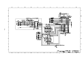
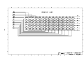
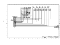
6-4. Memory chip selection circuit
The RAM chip select signals made by the following circuit.
There are 4 chip enable signal lines for RAM selection and 3 chip enable signal lines for
Flash ROM selection (including Memory cassette).
RAM1 CE
RAM2 CE
RAM3 CE
RAM4 CE
RAM1 CE is for
RAM 1 chip enable signal.
RB1
RB2
RB3
RB4/CB1
FB1
RAM enable
ARC RESET
RAM1 selection
The RAM1 is selected by the RAM enable signal "H" and the 2CS signal " L" of output pin
No.13 . The 2SC signal becomes "L" when the CPU address is as follows:
A19 A18 A17 A16 A15 A14 A13 A12 A11 A10 A9
L
L
H
L
X
X
X
X
X
X
X
2
X
A8
X
A7
X
X
A6
X
A5
X
A4
X
A3
X
X
A2
X
A1
X
A0
X
X
Also, the 3SC signal becomes "L" when the CPU address is as follows:
A19 A18 A17 A16 A15 A14 A13 A12 A11 A10 A9
L
L
H
H
X
X
X
X
X
X
X
3
X
A8
X
A7
X
X
A6
X
A5
X
A4
X
A3
X
X
A2
X
A1
X
A0
X
X
Therefore, the RAM1 CE will active when the CPU adress is from 20000H to 3FFFFH with
RAM enable signal "H".
Flash ROM1 selection
The Flash 1 CE will active by the IC25 output pin No.3. This is inverted signal of A19.
A19 A18 A17 A16 A15 A14 A13 A12 A11 A10 A9
H L
L
L
X
X
X
X
X
X
X
8
X
X
A8
X
A7
X
A6
X
A5
X
X
A4
X
A3
X
A2
X
A1
X
A0
X
X
Therefore, the Flash1 CE will active when the CPU adress is from 80000H to FFFFFH.
- 13 -
6-5. Flash ROM1 address circuit
The Flash ROM1 address signals FA17 to FA20 are made by the following circuit.
The Flash ROM1 (LH28F016SCT-L95, 16M bits) is used for the application program.
Flash ROM1 (16M bits)
CPU address
A19 A18 A17
H
L
L
L
H
H
L
BANK port
FC2 FC1
L
L
L
L
H
X
FC0
L
H
X
BANK
H
L
L
X
L
H
X
3 H
4 H
Common L
H
H
H
H
X
Flash
FA20
0 L
1 L
2 A18
memory address
FA19 FA18 FA17
L
A18
A17
H
A18
A17
A17
L
L
L
H
L
A18
A18
L
A17
A17
L
NOTE
Memory block No. 8M bank 16M bank
02 to 07
0A to 0F
08,09
10,11,18,19
12 to 17
1A to 1F
00,01
Common
6-6. Flash ROM2 circuit
The Flash ROM2 is mounted to the small PCB E475-FLS. The PCB E475-FLS is
connected to connector CN10 of the Main PCB E475-1.
Fixed by one screw
Flash ROM2 (512 K bytes)
PCB E475-FLS
- 14 -
6-7. Flash Pack circuit (Memory Cassette RAC-9)
The Memory Cassette RAC-9 (2 M bytes) is possible to connect to the Flash Pack connector
CN17 of the Main PCB E475-1.
[RAC-9 circuit diagram]
Flash Pack connector
- 15 -
6-8. Memory map
The memory table is as follows:
RAM enable
H
H
H
H
H
H
L
X
X
X
X
H
H
2CS 3CS 4CS 8CS CCS A18 A19 RAM BANK
No. RB0
L
H
H
H
H
L
L
COM X
H
L
H
H
H
L
L
COM X
H
H
L
H
H
H
L
0 L
1 H
H
H
L
H
H
H
L
L
H
H
H
L
H
H
H
L
L
H
H
H
L
H
H
H
L
2 L
3 H
4 L
5 H
6 L
7 H
8 L
9 H
10 L
11 H
12 L
13 H
14 L
15 H
16 L
17 H
X
X
X
X
X
X
X
X
H
H
L
H
H
H
L
H
H
H
H
L
H
H
H
L
L
H
L
H
L
H
L
H
H
H
L
H
H
H
L
X
X
H
H
H
L
H
L
H
X
X
H
H
H
L
H
L
H
X
H
H
H
H
L
H
H
X
RB1
X
X
H
H
L
L
H
H
L
L
H
H
L
L
H
H
L
L
H
H
L
L
H
H
X
L
L
L
L
L
L
L
L
L
L
L
L
X
X
X
X
RB2
X
X
L
L
H
H
H
H
L
L
L
L
H
H
H
H
L
L
L
L
H
H
H
H
X
L
L
L
L
L
L
L
L
L
L
L
L
X
X
X
X
RB3
X
X
L
L
L
L
L
L
H
H
H
H
H
H
H
H
H
H
H
H
H
H
H
H
X
L
L
L
L
L
L
L
L
L
L
L
L
X
X
X
X
RB4
X
X
X
X
X
X
X
X
L
L
L
L
L
L
L
L
H
H
H
H
H
H
H
H
X
X
X
L
L
H
H
L
L
H
H
X
X
X
X
X
X
Flash BANK
FB0 FB1 FB2
X
X
X
X
X
X
X
X
X
X
X
X
X
X
X
X
X
X
X
X
X
X
X
X
X
X
X
X
X
X
X
X
X
X
X
X
X
X
X
X
X
X
X
X
X
X
X
X
X
X
X
X
X
X
X
X
X
X
X
X
X
X
X
X
X
X
X
X
X
X
X
X
X
X
X
L
H
L
H
H
L
L
L
L
L
L
L
L
L
L
L
L
L
H
L
L
H
L
L
H
L
L
H
L
L
L
X
H
H
X
H
L
X
H
H
X
H
X
X
L
X
X
X
RAM1
C S A16
L
L
L
H
H
X
H
X
H
X
H
X
H
X
H
X
H
X
H
X
H
X
H
X
H
X
H
X
H
X
H
X
H
X
H
X
H
X
H
X
H
X
H
X
H
X
H
X
H
X
H
X
H
X
H
X
H
X
H
X
H
X
H
X
H
X
H
X
H
X
H
X
H
X
H
X
H
X
H
X
H
X
RAM2
C S CS2
H
H
H
H
L
H
L
H
H
H
H
H
H
H
H
H
H
H
H
H
H
H
H
H
H
H
H
H
H
H
H
H
H
H
H
H
H
H
H
H
H
H
H
H
H
H
H
H
H
L
H
H
H
H
H
H
H
H
H
H
H
H
H
H
H
H
H
H
H
H
H
H
H
H
H
H
H
H
H
H
H
H
A16
X
X
L
H
X
X
X
X
X
X
X
X
X
X
X
X
X
X
X
X
X
X
X
X
X
X
X
X
X
X
X
X
X
X
X
X
X
X
X
X
X
RAM3
C S A16
H
X
H
X
H
X
H
X
H
X
H
X
H
X
H
X
L
L
L
H
L
L
L
H
L
L
L
H
L
L
L
H
H
X
H
X
H
X
H
X
H
X
H
X
H
X
H
X
H
X
H
X
H
X
H
X
H
X
H
X
H
X
H
X
H
X
H
X
H
X
H
X
H
X
H
X
H
X
H
X
H
X
A17
X
X
X
X
X
X
X
X
L
L
H
H
L
L
H
H
X
X
X
X
X
X
X
X
X
X
X
X
X
X
X
X
X
X
X
X
X
X
X
X
X
A18
X
X
X
X
X
X
X
X
L
L
L
L
H
H
H
H
X
X
X
X
X
X
X
X
X
X
X
X
X
X
X
X
X
X
X
X
X
X
X
X
X
RAM4
C S A16
H
X
H
X
H
X
H
X
H
X
H
X
H
X
H
X
H
X
H
X
H
X
H
X
H
X
H
X
H
X
H
X
L
L
L
H
L
L
L
H
L
L
L
H
L
L
L
H
X
X
H
X
H
X
H
X
H
X
H
X
H
X
H
X
H
X
H
X
H
X
H
X
H
X
H
X
H
X
H
X
H
X
A17
X
X
X
X
X
X
X
X
X
X
X
X
X
X
X
X
L
L
H
H
L
L
H
H
X
X
X
X
X
X
X
X
X
X
X
X
X
X
X
X
X
A18
X
X
X
X
X
X
X
X
X
X
X
X
X
X
X
X
L
L
L
L
H
H
H
H
X
X
X
X
X
X
X
X
X
X
X
X
X
X
X
X
X
Flash1
C S A18
H
X
H
X
H
X
H
X
H
X
H
X
H
X
H
X
H
X
H
X
H
X
H
X
H
X
H
X
H
X
H
X
H
X
H
X
H
X
H
X
H
X
H
X
H
X
H
X
X
X
H
X
H
X
H
X
H
X
H
X
H
X
H
X
H
X
H
X
H
X
H
X
H
X
H
X
H
X
L
A18
L
A18
Flash2
C S A18
H
X
H
X
H
X
H
X
H
X
H
X
H
X
H
X
H
X
H
X
H
X
H
X
H
X
H
X
H
X
H
X
H
X
H
X
H
X
H
X
H
X
H
X
H
X
H
X
X
X
L
L
L
H
H
X
H
X
H
X
H
X
H
X
H
X
H
X
H
X
H
X
H
X
H
X
H
X
H
X
H
X
Flash pack
C S A18
H
X
H
X
H
X
H
X
H
X
H
X
H
X
H
X
H
X
H
X
H
X
H
X
H
X
H
X
H
X
H
X
H
X
H
X
H
X
H
X
H
X
H
X
H
X
H
X
X
X
H
X
H
X
L
L
L
H
L
L
L
H
L
L
L
H
L
L
L
H
H
X
H
X
H
X
H
X
H
X
H
X
A19
X
X
X
X
X
X
X
X
X
X
X
X
X
X
X
X
X
X
X
X
X
X
X
X
X
X
X
L
L
H
H
L
L
H
H
X
X
X
X
X
X
A20
X
X
X
X
X
X
X
X
X
X
X
X
X
X
X
X
X
X
X
X
X
X
X
X
X
X
X
L
L
L
L
H
H
H
H
X
X
X
X
X
X
Memory map
00000h CPU internal memory
Mask ROM 128K
RAM 5K
0FFD0h External I/O Mapping 16bytes
0FFE0h
20000h
RAM1 128 K bytes
RAM2
Oprion RAM3
Oprion RAM4
128 K bytes
512 K bytes
512 K bytes
Bank0 Bank1 Bank2 Bank3 Bank4 Bank5 Bank6 Bank7 Bank8 Bank9 Bank10 Bank11 Bank12 Bank13 Bank14 Bank15 Bank16 Bank17
40000h
RAM
Banked area
64 K bytes
Flash2
Flash pack
Expansion memory
256 K bytes
Flash2
512K bytes
512 K bytes
Flash memory pack
Bank0 Bank1
Bank0 Bank1 Bank2 Bank3 Bank4 Bank5 Bank6 Bank7
80000h
Bank area
Flash 1
384 K bytes
(for
A0000h Application
program area)
2 M bytes
16 M bit
8 M bit
4 M bit
Bank0 Bank1 Bank2 Bank3 Bank4
00,01 08,09 14,15 20,21 26,27
(07,06) (0F,0E) (19,18) (17,16) (1F,1E)
Block No.
(Memory Block)
C0000h
02,03 10,11 16,17 22,23 28,29
(05,04) (0D,0C) (11,10) (15,14) (1D,1C)
E0000h
FFFFFh
Common area
128 K bytes
Block
06,07
(00,01)
04,05 12,13 18,19 24,25 30,31
(o3,02) (0B,0A) (09,08) (13,12) (1B,1A)
- 16 -
2 M bytes
Accelerator
Board
Share CE
+ A16 to A19
Expansion Memory area
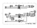
6-9. Printer drive circuit
The printer drive circuit is as follows:
IC5 (MTA001M-F4101) is the head pin driver IC. And, the Transistors Q6,Q7 and Q8 are the
motor drive circuit. The IC1 (TA8429H) is the auto paper cut driver circuit.
6-10. RS232C port COM1 circuit
The COM1 circuit is as follows:
The COM1 port pin location is as shown below:
Signal
CD
RxD
TxD
DTR
GND
DSR
RTS
CTS
CI
Pin
1
2
3
4
5
6
7
8
9
1
2
6
3
7
- 17 -
4
8
5
9
6-11. RS232C port COM2 and COM3 circuit
The circuits of COM2 and COM3 are as follows:
TP48
COM2
COM3
The COM2, and COM3 port pin locations are as shown below:
COM2 port
Signal
Pin
NC
1
RxD
2
TxD
3
DTR
4
GND
5
DSR
6
RTS
7
CTS
8
VCC(+5V)
9
COM3 port
Signal Pin
NC
1
RxD
2
TxD
3
DTR
4
GND
5
DSR
6
RTS
7
CTS
8
NC
9
1
2
6
- 18 -
3
7
4
8
5
9
6-12. Keyboard selection switch
The main PCB has the keyboard selection switch to detect the keyboard type.
For the model CE-7000, set the switch to S position for the stroke key type.
Keyboard selection switch
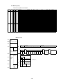
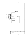
6-10. To mount optional circuit
The following optional circuits are provided for this model.
1. Clerk key circuit
2. Multi-drawer circuit
3. Paper near end sensor circuit
1) Clerk key circuit
NOTE1 : This circuit is mounted from factory for the destination Germany.
NOTE2 : It is not option item for USA and Canada.
1-1. Prepare the following parts kit for clerk key circuit. The follwing parts kits are supplied from
sales division.
CLK-K19
CLK-K20
CLK-K21
Clerk key kit for 4 clerks
Clerk key kit for 6 clerks
Clerk key kit for 15 clerks
1-2. Check whether the parts of clerk kit are as follows:
Code No.
10003976
34002576
62482225
38401238
62158913
51115760
55600368
30304055
10017367
10003979
10011117
10003980
10011785
Parts Name
Clerk unit sub ass'y
Clerk key switch unit
Cleak key cable sub ass'y
FG wire fixing pin
FG wire
Screw
Insulok tie
Ferrite core
Clerk key case
Clerk key set (4keys)
Mode key plate
Clerk key set (6keys)
Clerk key set (15keys)
Specification
Q'ty
E340843A*1
1
J-Y7541
1
E440785B*1
1
23031-1
1
E32406-2
1
2.6 x 8 ZMC-3
1
T-18S
2
L5T18 x 6 x 10
1
E311204A-2
1
306JYB-135-02R
1
E340735A-23
1
306JYB-135-01R
1
306JYB-135-03R
1
- 19 -
1-3. Connect the clerk key cable sub ass'y to the clerk key unit. Also, fix the FG wire by the fixing
pin and the screw.
Clerk cable sub ass'y
Clerk key unit
Pin No. Wire color Printed mark on PCB
1
Red
C
2
White
1
3
Blue
2
4
Yellow
4
5
Green
8
1-4. Insert the clerk switch unit to the clerk key case.
Turn 2 times
Ferrite core
Clerk key case
1-5. Cut off the masking plate of clerk key unit of lower case. Then, set the clerk key case and
unit to the lower case.
Connect the connector cable
to the Main PCB.
Lower case
Fix the FG wire from cleark key
unit this position.
Clerk key unit
- 20 -
Clerk key case
1-6. Remove the clerk button unit form the upper case. Then, replace the model key plate.
Remove the mode key plate. Then,
fix new mode key plate.
Upper case
2) Multi-drawer kit
2-1. Prepare the following parts kit for multi-drawer circuit. The parts kits are supplied from sales
division.
MDL-10
Multi-drawer kit
2-2. Check whether the parts of multi-drawer kit are as follows:
Code No. Parts Name
10006121 Drawer connector cable
62481534 Extension cable for Drawer
59000209 Screw
Specification
E440721A*1
E440714*1
3X4ZMC-3.
Q'ty
1
1
1
2-3. Connect the drawer connector cable to the main PCB by solder.
Drawer2
Drawer3
Drawer4
Red
Brown
Black
- 21 -
2-4. Open the back cover of lower cabe to release the 2 screws. Then, connect the necessary
extension cable for drawer. In this case, do no forget to fix the FG wire of the extension
cable to the frame ground by the screw.
Release the 2 screws and open the
back cover of lower case.
Connect the extension
drawer cable to the
drawer connector.
Fix the FG wire of the
extension drawer cable by
screw of the parts kit.
2-5. Connect 1 pin FG connector of the drawer extension cable to the drawer 1 pin connector.
Close the back cover of lower case by 2 screws.
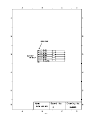
3) Paper near end sensor curcuit
3-1. Prepare the following parts for paper near end sensor circuit. The individual parts are
supplied from spare parts sales department same as an other spare parts.
Code No.
19076948
19030101
62366288
19077906
35401431
Parts Name
Paper end sensor
Adjustment screw
Sensor holder
Screw
Pin assembly 2P
Specification
C33-651000
C109302051
E410223B-02
3 x 8 ZMC-3
5045-02A
3-2. Mount the pin assembly 2P to the main PCB.
Mount 2P Pin
assembly
- 22 -
Q'ty
1
1
1
2
1
3-3. Fix the paper near end sensor to the lower case by 2 screws and connect the sensor
connector to the main PCB.
1903 0101
19077906
62366288
1907 6948
Main PCB
2P connector
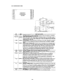
6-14. Display controller uPD78015FGC526-AB8
- 23 -
Pin No.Signal Name Description
1 TO0
BLINK OUT
2 TO1
BK1 SIGNAL
3 TO2
BK2 SIGNAL
4 TI1
SIG
5 TI2
CLKG
6 PCL
BK
7 BUZ
LAT1/LAT2
8 P37
VFD RS
9 VSS
GND
10 AD0
CONNECTED TO GND
11 AD1
CONNECTED TO GND
12 AD2
CONNECTED TO GND
13 AD3
CONNECTED TO GND
14 AD4
CONNECTED TO GND
15 AD5
CONNECTED TO GND
16 AD6
CONNECTED TO GND
17 AD7
CONNECTED TO GND
18 A8
CONNECTED TO GND
19 A9
CONNECTED TO GND
20 A10
CONNECTED TO GND
21 A11
CONNECTED TO GND
22 A12
CONNECTED TO GND
23 A13
CONNECTED TO GND
24 VSS
GND
25 A14
CONNECTED TO GND
26 A15
CONNECTED TO GND
27 P60
CONNECTED TO GND
28 P61
CONNECTED TO GND
29 P62
CONNECTED TO GND
30 P63
CONNECTED TO GND
31 RD
CONNECTED TO GND
32 WR
CONNECTED TO GND
In/Out
Out
Out
Out
Out
Out
Out
Out
In
Pin No.
33 WAIT
34 ASTB
35 RESET
36 INTP0/TI0
37 INTP1
38 INTP2
39 INTP3
40 VDD
41 X2
42 X1
43 IC
44 XT2
45 XT1
46 AVSS
47 ANI0
48 ANI1
49 ANI2
50 ANI3
51 ANI4
52 ANI5
53 ANI6
54 ANI7
55 AVDD
56 AVREF
57 SI1
58 SO1
59 SCK1
60 STB
61 BUSY
62 SI0/SB0
63 SO0/SB1
64 SCK0
In/Out
In/Out
In/Out
In/Out
In/Out
In/Out
In/Out
In/Out
Out
Out
Out
Out
Out
Out
Out
Out
In/Out
In/Out
In/Out
In/Out
Out
Out
Description
CONNECTED TO GND
CONNECTED TO GND
VFD RESET SIGNAL
VFD BK
VFD CE
VFD WR
SOG
VCC
CLOCK INPUT
CLOCK INPUT
CONNECTED TO GND
NOT USED
CONNECTED TO GND
CONNECTED TO GND
VFD D0
VFD D1
VFD D2
VFD D3
VFD D4
VFD D5
VFD D6
VFD D7
VDD
CONNECTED TO VDD
CONNECTED TO GND
SI1/SI2
SCLK1/SCLK2
CHIP ENABLE FOR uPD16312GB-3B4
VFD BUSY
CONNECTED TO GND
SO SIGNAL TO uPD16312GB-3B4
SCK SIGNAL FOR uPD16312GB-3B4
In/Out
In
Out
In
In
In
In
In
In
In
In
In
In
In
In
In
In
In
In
In
In
In
In/Out
Out
In
In
Out
In/Out
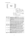
6-15. Segment display driver uPD16312GB-3B4
Key data memory
Segment driver
Common driver
Shift register
Timing Generator
Key Scanning
Grid driver
Display memory
Data selector
Serial
Dimmer
Output latch
Command decorder
Latch
Latch
Pin No.Signal NameDescription
1 SW1
CONNECTED TO GND
2 SW2
CONNECTED TO GND
3 SW3
CONNECTED TO GND
4 SW4
CONNECTED TO GND
5 DOUT
NOT USED
6 DIN
SO
7 VSS
GND
8 CLK
SCK
9 STB
CE
10 KEY1
CONNECTED TO GND
11 KEY2
CONNECTED TO GND
12 KEY3
CONNECTED TO GND
13 KEY4
CONNECTED TO GND
14 VDD
VCC
15 SEG1
SEGMENT SIGNAL SA
16 SEG2
SEGMENT SIGNAL SB
17 SEG3
SEGMENT SIGNAL SC
18 SEG4
SEGMENT SIGNAL SD
19 SEG5
SEGMENT SIGNAL SE
20 SEG6
SEGMENT SIGNAL SF
21 SEG7
SEGMENT SIGNAL SDP
22 SEG8
SEGMENT SIGNAL SG
In/Out
In
In
In
In
Out
In
In
In
In
In
In
In
Out
Out
Out
Out
Out
Out
Out
Out
- 24 -
Pin No.Signal NameDescription
23 SEG9
SEGMENT SIGNAL SH
24 SEG10
SEGMENT SIGNAL SCOM
25 SEG11
NOT USED
26 SEG12
NOT USED
27 VEE
VN
28 GRID10
DIGIT SIGNAL SG10
29 GRID9
DIGIT SIGNAL SG9
30 GRID8
DIGIT SIGNAL SG8
31 GRID7
DIGIT SIGNAL SG7
32 GRID6
DIGIT SIGNAL SG6
33 GRID5
DIGIT SIGNAL SG5
34 GRID4
DIGIT SIGNAL SG4
35 GRID3
DIGIT SIGNAL SG3
36 GRID2
DIGIT SIGNAL SG2
37 GRID1
DIGIT SIGNAL SG1
38 VDD
VCC
39 LED4
NOT USED
40 LED3
NOT USED
41 LED2
NOT USED
42 LED1
NOT USED
43 VSS
GND
44 OSC
CLOCK SIGNAL TERMINAL
In/Out
Out
Out
Out
Out
Out
Out
Out
Out
Out
Out
Out
Out
Out
In
6-16. DC/DC converter circuit
There are two DC/DC convertor circuit for
display.
For the 7 segment display voltages are
made by the DC/DC converter in display
PCB E445B-E2. Transistor Q3 is oscillating
and zener diode ZD3 feedbacks the output
voltage to control the oscilation.
VC
For the dot display voltages are made by the
DC/DC converter in display PCB E445B-E2.
Transistor Q1,Q2 ,IC6 and DC/DC converter
transformer T1.
The dot display MN12832E need the
following Voltages.
1. Filament Voltage
VD1,VD2 = AC4.8V
2. Logic Volatge
VCC= DC5V
3. Display Voltage
VD3 = DC58V
6-17. ARCNET circuit (I/O PB14)
For the model CE-7000, the ARCNET board I/O PB14 is installed from the factory.
It is possible to connect up to 32 units without scanning system (scanning system up to
4 units) through the ARCNET In-line connection.
1. ARCNET CHIP COM20019ILJP
- 25 -
Pin No.Pin Name N a m e
1 A0/nMUX
2 A1
3 A2/ALE
4
5
6
8
9
10
11
12
AD0
AD1
AD2
D3
D4
D5
D6
D7
27 nRD/nDS
26 nWR/DIR
23 nRESET
24 nINTR
25 nCS
18 nPULSE1
19 nPULSE2
In/Out Status of OFF Status of ON Status of ON Description
No Token
Token
Address 0-2 In
L
L
Pulse
On a non-multiplexed bus,
these signals are directly
connected to the lower 3
bits of the address bus. on
the multiplexed address /
data bus, A0/nMUX is tied
low, A1 is left open, and
A2 is tied to the address
latch enable signal of the
host. A1is connected to an
internal pull-up resistor.
Data 0-7
In/Out L
Pulse
Pulse
Input/Output. On a nonIn/Out L
Pulse
Pulse
multplexed bus, these
In/Out L
Pulse
Pulse
signals are used as the
In/Out L
Pulse
Pulse
lines fo the device. On a
In/Out L
Pulse
Pulse
multiplexed address/data
In/Out L
Pulse
Pulse
bus, AD-AD2 act as the
In/Out L
Pulse
Pulse
address lines (latched by
In/Out L
Pulse
Pulse
ALE) and as the low data
lines for the device. D3-D7
are always used for data
only. These signals are
connected to internal pullup resistors.
nRead/ nData In
L
L
Pulse
Read/Data strobe signal
Strobe
input. On a 68xx-like bus,
this active low signal is
issued by the
microcontroller as the data
strobe signal to strobe the
data onto the bus.
On a 80xx-like bus, this is
active low signal is issued
by the microcontroller to
indicate a read operation.
nWrite/
In
L
Pulse
Pulse
Input. On a 68xx-like bus,
Direction
this signal is issued by the
microcontroller as the
Read/Write signal to
determine the direction of
the transfre.
In this case, a logic "1"
selects a read operation,
while a logic "0" selects a
write operation. In this
case, data is actually
strobed by the DS signal.
On a 80xx-like bus, this
active low signal is issued
by the microcontroller to
indicate a write operation.
In this case a logic "0" on
this pin, when the
COM20019 is accessed,
enables data from the
data bus to be written to
the device.
nReset IN
In
L
H
H
Input. This active low
signal
issued by the microcontroller executes a
hard- ware reset. It is used
to active the internal reset
circuitry within the
COM20019.
nInterrupt
Out
L
H
Pulse
Interrupt output. This
active low signal is
generated by the
COM20019 when an
enabled interrupt
condition occurs.
INTR returns to its
intactive state when the
interrupt status condition
or the corresponding
interrupt mask bit is reset.
nChip Select In
L
H
Pulse
Chip select input. This
active low signal issued
by the microcontroller
selects the COM20019 for
an access.
nPulse1
Out
L
H
Pulse
Output. When the device
is
nPulse2
Out
L
L
L
in backplane mode, the
nPULSE1 signal driver is
programmable( push/pull
High= -2mA, Low= 4mA or
open drain ). nPULSE1 is
connected to a week
internal pull-up resistor in
backplane mode.
nPULSE2 becomes
double size of data rate
syncronized clock output.
When nPULSE2 is N/C,
nTXEN is active low. But,
power up time, when
nPULSE" is connected to
GND, the nTXEN terminal
becomes active high.
- 26 -
Pin No.Pin Name N a m e
20 RXIN
21 nTXEN
16 XTAL1
17 XTAL2
15
28
7
14
22
VDD
VDD
VSS
VSS
VSS
In/Out Status of OFF Status of ON Status of ON Description
No Token
Token
Receive IN
In
L
H
Pulse
Receive input. This signal
carries the receive data
information from the line
receiver circuitry to the
COM20019.
nTransmit
Out
L
L
Pulse
Transmit Enable output.
Enable
This signal used in
backplane mode to
enable the line driver for
transmission. The polarity
of the signal is
programmable by
grounding the nPULSE2
pin.
Normally, connect nTXEN
terminal of HYC2488S or
DE terminal of RS485
driver.
Crystal
In
L
Pulse
Pulse
An external crystal should
Oscillator
In
L
Pulse
Pulse
be connected to these pin.
If an external TTL clock is
used instead of C-MOS
level, it must be connected
to XTAL1 with 390 ohms
pull-up resistor, and
XTAL2 should be left
floating.
Power supply Power GND
(+5V)
(+5V)
Power supply +5V
Power GND
(+5V)
(+5V)
Powersupply Power GND
GND
GND
Power supply GND
Power GND
GND
GND
Power GND
GND
GND
2. ARCNET In-line circuit
The In-line circuit is as follows:
CE-7000 has the ARCNET In-line
board I/0 PB-14.
ARCNET In-line circuit
board I/0 PB-14
- 27 -
3. In-line connection
1) System connection diagram
The maximum In-line (ARCNET) cable length and maximum connection unit will be
varied by the In-line communication speed as shown below:
NOTE: The terminater 100 ohms is necessary to mount at the end of In-line cable .
Total In-line cable length is max. A m.
Terminater (100 ohms)
Terminater (100 ohms)
In line communication speed
(Baud rate)
Maximum
connection unit
Maximum
cable length A ( m )
312.5 K bps
156.25 K bps
20 units
32 units
430 m
890 m
2) In-line cable and connector
CASIO TECHNO will supply the In-line cable, connector and terminater parts by the
following parts code.
In line cable
Code No.
1904 4023
Parts name
In-line cable
Specification
IPEV-SLA0.5x1P
Parts name
In-line connector kit
Specification
XLP-KIT-1
Parts name
Carbon film resistor
Specification
R-25-100-J
In line connector
Code No.
3500 5820
Terminater
Code No.
2600 2516
3) In-line cable connection
In-line cable connection diagram is shown below:
Mount the terminater 100 ohms at the both end of In-line cable.
Signal
SD
Pin
1
RD
2
FG
FG plate
(In-line connector)
Terminater
100 ohms
Signal
SD
Pin
1
Signal
SD
Pin
1
RD
2
RD
2
FG
FG plate
(In-line connector)
- 28 -
FG
FG plate
(In-line connector)
Terminater
100 ohms
4) To connect the In-line cable
Connect the In-line cable and connector as shown below:
Connector at the enc of In-line cable
Terminal cap
Red
In-line connector
In-line cable
Wrap bent shield wire
with Copper tape.
Black
Shield wire
Terminater (100 ohms)
Notes:
1. Use crimp tool for connecting terminal caps.
2. If crimp tool is not available, connect the wires
with solder instead of terminal cap. After the
soldering, insulate the wires with vinyl tape.
Connector at the enc of In-line cable
Terminal cap
Red
In-line connector
In-line cable
Wrap bent shield wire
with Copper tape.
Black
Shield wire
Notes:
1. Use crimp tool for connecting terminal caps.
2. If crimp tool is not available, connect the wires
with solder instead of terminal cap. After the
soldering, insulate the wires with vinyl tape.
- 29 -
In-line port
(ARCNET)
Release the 2 screws to remove
the bachk cover.
Connect the In-line
cable shield wire to
FG plate.
To connect the In-line cable, release the 2 screws from the back cover.
Then, remove the Back cover. And, put the In-line connector to the ARCNET In-line port.
Do not foget to connect the shield wire (copper tape part) to the FG plate by the cable
supporter with screw.
5) Specification of the In-line cable
1. Structure
Conductor
Insulation
Sheath
Material:
Cross section area:
Construction:
O.D.
Material:
Thickness
Material:
Thickness
Finished O.D.:
Approx. weight:
Tin plated mild copper twist
0.5mm2
20 pieces/0.18 mm
0.95 mm
Polyethylene
0.3 mm
PVC
1.3 mm
6.0 ~6.5 mm
55 kg/km
2. Properties (20°C)
Maximum conductor resistance
Minimum insulation resistance
Electric strength
Electrostatic capacity (Standard)
38.7 Ω/km
10 kMΩ•km
AC350 V/1 minute
75 nF/km
- 30 -
7. DIAGNOSTIC OPERATION
7-1. To start the diagnostic program
1. Plug the power cord into an AC outlet.
2. Set the mode switch to "OFF" position.
3. While pressing the "Jounal feed " button,
turn the mode switch to "PRG" position.
4. Release the "Journal feed" button.
5. Input "99990000" and press "ST" ("#2" key).
6. Diagnostic program is executed.
7-2. Check item
The following test can be checked in the diagnostic test.
1. Key code test
2. Switch status test
3. Individul function test
7-3. Operation of each test
1. Key code test
When pressing a key, the machine displays
the following key code.
DISPLAY
X X X
z
Hard key code
089
HARD KEY CODE TABLE
Key borad information
11: Stroke Key
10: Stroke + Flat Key
01: Full Flat Key
090
091
092
093
094
095
096
097
098
099
100
RF
JF
077
070
068
066
066
060
054
048
042
036
030
024
018
087
082
076
069
067
065
065
059
053
047
041
035
029
023
017
086
081
075
7
8
9
064
058
052
046
040
034
028
022
015
085
080
074
4
5
6
063
057
051
045
039
033
027
014
016
084
079
073
1
2
3
062
056
050
044
038
032
026
020
021
083
078
072
0
11
12
061
055
049
043
037
031
025
019
013
Note: "014" button is work for "#2" key. "013" button is work for "#1" key.
- 31 -
z
7-4. Switch status test
Press "C" button or changing the switch condition,the switch status is appeared on the
transaction place of the display. The clerk key switch condition is shown at the 6 and 7 digit
number's place of display. For the clerk button model, the pressed LED will light on.
[DISPLAY]
Allways off
Allways off
Allways off
NOTE: Journal TAIWAN sensor
Off: No mark position
On: Mark position
Allways off
NOTE: Receipt TAIWAN sensor
Off: No mark position
On: Mark position
Allways off
NOTE: Validation sensor (Not used)
Off: Normal
On: Validation paper in
ROM cassette condition
Off : Not mounted
On : Mounted
Clerk key condition (Germany)
00 : Not inserted key
01 to 16 : Clerk key number
Paper near end sensor
Off : Normal (Paper end switch OFF)
On : Near end (Paper and switch ON)
Drawer sensor
Off : Drawer close
On : Drawer open
Menu switch conditon (Only for TK6000 and TK7000)
0 : Switchs are both off condition.
1 : Menu 1
2 : Menu 2
Mode switch status
0 : No connetion
1 : PGM
2 : RF
3 : REG1
4 : REG2
5:X
6:Z
7 : XZ2
8 : OFF
- 32 -
7-5. Individual function test
1) Series test
This test will perform the following tests in series.
1. Display test (All dot and segment trun on.)
2. RAM read after write test (one time)
3. Print test (one time)
4. Time display test
5. Drawer open test
6. Receipt issue test
7. Display test (1234567890 display)
Operation :
X
1
#2
Key
Function X : 0= Automatic RAM capacity detection
1= RAM1 (128K) test only
2= RAM1,2 (128K) test
4= RAM1,2,3 (RAM3 is 512K.) test
6= RAM1,2,3,4 (RAM3,4 are 512K.) test
[PRINT]
[DISPLAY]
NOTE : In case of error, the following error message will be printed.
RAM1 128K WR ERR!! 00 000000 -----------When the write error is happened.
Error Bank and Address
RAM1 128K RD ERR!! 00 000000 ------------When the verified data error is happened.
FLASH SUM ERR!!
1234 ------------Check sum of Flash1 is not "FFFF".
Caliculated check sum
- 33 -
2) Print aging test (R/J printer)
This test will check the R/J printer continuously until pressing some key button or turn off
the mode switch.
Operation : n1
Y
X
2
#2 Key
X: 0= Print 45 times test pattern without paper cut in a minute.
1= Print 15 times test pattern with paper cut in a minute.
Y: 0= Normal print
1= Continuously print
n1: 0= Display test pattern
1= All dots and segment will light on.
[PRINT]
[DISPLAY]
Dot display (Test pattern)
3
TL $3,024
SHAMPOO
Segment display (Test pattern)
3) Print aging test (Slip printer)
This test will check the slip printer continuously until pressing some key button or turn off
the mode switch.
Operation : n3 n2
n1 Y
1
2
#2 Key
Y: 0= Normal print
1= Continuously print
n1: 0= Display test pattern
1= All dots and segment will light on.
n2: 0= Print R/J printer
1= Non print R/J printer
n3: 0= Port selection Com2
1= Port selection Com3
4) Print aging test (Kitchen printer)
When the machine is opened for the kitchen printer port with connection of the kitchen
printer, the kitchen printer will print by the same command of R/J printer aging test.
[Open command]
Operation : s
b
1
9
2
0
7
#2 Key
b: 0= 19,200bps 1= 9,600bps 2= 4,800bps 3= 2,400bps
s: 0= Com1
1= Com2
2= Com3
[Close command]
Operation : 2
9
2
0
7
#2 Key
- 34 -
5) Print test (R/J printer)
This test will check the R/J printer. To stop the continuous printing, press some key
button or turn off the mode switch.
Operation : n1
n
0
X
0
#2 Key
X: 0= One time print
1= Continuously print
n: 0= Display test pattern
1= All dots and segment will light on.
n1: 0= Print test pattern
1= Print all "B"
[PRINT]
[DISPLAY]
Dot display (Test pattern)
3
TL $3,024
SHAMPOO
Segment display (Test pattern)
Print all "B"
Print test pattern
6) Print aging test (Slip printer)
This test will check the slip printer. To stop the continuous printing, press some key
button or turn off the mode switch.
Operation : n2 n1
n
0
X
0
#2 Key
X: 0= Normal print
1= Print slip printer
n: 0= Display test pattern
1= All dots and segment will light on.
n1: 0= 35 characters print
1= Non print R/J printer
2= 42 characters print
n2: 0= Port selection Com2
1= Port selection Com3
7) Print aging test (Kitchen printer)
When the machine is opened for the kitchen printer port with connection of the kitchen
printer, the kitchen printer will print by the same command of R/J printer test.
[Open command]
Operation : s
b
1
9
2
0
7
#2 Key
b: 0= 19,200bps 1= 9,600bps 2= 4,800bps 3= 2,400bps
s: 0= Com1
1= Com2
2= Com3
[Close command]
Operation : 2
9
2
0
7
#2 Key
- 35 -
8) Flash1 ROM check
This test will check the Flash 1 ROM. This test will print the version name and check
sum on the receipt as shown in sample print. When using several bank, the each version
name and check sum will be printed after this sample data.
Operation :
9
0
0
#2 Key
[PRINT]
[DISPLAY]
Dot display
DIAG MODE
QA version
Segment display
9) Printer auto paper cut check
This test will check the auto paper cut function.
Operation : 3
n
0
#2 Key
n: 0= Full cut (one line paper feed)
1= Half cut (no paper feed)
[PRINT]
[DISPLAY]
Dot display
DIAG MODE
QA version
Full cut (command = 300)
Segment display
Half cut (command = 310)
10) Drawer open check
This test will check the drawer open function.
Operation : d3 d2 d1
8
n
0 #2 Key
n: 0= Open drawer without print.
2= Open drawer with print 10lines "B" printing.
NOTE1: d3,d2,d1 are option drawer test. When input the following number, the option
drawer will be opened.
2= drawer2
3= drawer3
4= drawer4
NOTE2: Command 800 is open drawer1.
- 36 -
11) Flash2 ROM and Flash pack check
This test will check the Flash 2 ROM and Flash pack. This test will perform the erase,
write, and verify check.
Operation :
n1 n2
s
n
X
3
#2 Key
s: 0= Select Flash2
1= Select Flash pack
X: 5= Test by one block (64 bytes)
Select the block by the Number n (from 0 to 9).
When the block is over 9, use the number n1 and n2.
6= Test the all block. After test, the all block data is cleared.
In this case, number n will have the following function select.
n: 1= Repeat check (After finished all block check, start the
check from 0 block again. To stop this check, set mode
switch to off position.)
2= Read only check (The erase and write test are not
performed in the each block. Therefore, perform the
erase and write test "command 263 #2" before this test.)
4= The erase and write test only. (Non data clear after test)
6= Blank check (check 0FFH)
NOTE1: During this test, the LED of receipt switch will blink. In the repeat test, the
machine will display the repeat count number on the segment display. When the
error is happened, the machine will issue an error receipt.
NOTE2: The erase, write and verify check will perform the following procedure.
And, the last step, the all block data will be cleared.
1) The designated block (64 Kbytes) will be erased.
( The data will be cleared after the block protect released. )
2) The test data will be stored in the block area ( 64 Kbytes ).
The test data is made by the test address/bank.
Test data (8bits) = Block No. + address(Middle 8 bits) + address(Lower 8 bits)
3) Verify the designated block ( 64 Kbytes ).
[PRINT]
[DISPLAY]
Dot display
ALL BLOCK ERASE/
WR OK
Segment display
Error address
The beginning address of Flash chip is
"000000".
Error receipt
ERASE ERR!!
WR ERR!!
RD ERR!!
no PACK ERR!!
WR PROTECT!!
000000
000000
000000
000000
040000
00
00
43
01
FF
Error code
Error code is made by Flash controller device.
- 37 -
12) Flash ROM and Flash pack device information check
This test will check the Flash ROM and Flash pack device infromation .
Thie device signature code (Maker code, device code) and write protect information will
be printed on the receipt.
Operation :
s
0
0
3
#2 Key
s: 0= Select Flash2
1= Select Flash pack
2= Select Flash1
[PRINT]
[DISPLAY]
Dot display
DEVICE ID
89A7
Segment display
Flash ROM signature code
89A7 = LH28F004SCT
89A6 = LH28F008SCT
89AA = LH28F016SCT
MASTER LOCK BIT
Allways "00"
EACH BLOCK LOCK BIT
00 = Non protection
01 = Protection
13) Flash2 ROM and Flash pack read only check
This test will check the read only check for Flash 2 ROM and Flash pack.
Perform the Flash memory check (command "n53 and #2" ), before start of this operation.
Operation :
s
0
0
4
#2 Key
s: 0= Select Flash2
1= Select Flash pack
[PRINT]
[DISPLAY]
Dot display
RD OK
01
Segment display
- 38 -
14) RAM read only check
This test will check the read only check for RAM.
Perform the RAM check (EX: command "1 and #2 " ), before start of this operation.
Operation :
X
5
#2 Key
X: 0= One time check.
1= Continuous check. To stop the test, set the mode switch to OFF.
NOTE: During the RAM test, the Receipt switch LED is blinking.
[PRINT]
[DISPLAY]
Dot display
Segment display
15) RAM read write check
This test will check the read write check for RAM.
Operation :
n
4
X
0
#2 Key
X: 0= Automatic RAM capacity detection
1= RAM1 (128K) test only
2= RAM2 (128K) test only
4= RAM3 (512K) test only
6= RAM4 (512K) test only
NOTE: RAM1 is always checked even if selected other RAM number.
[PRINT]
[DISPLAY]
Dot display
RAM4(OP)512K RD
OK
Segment display
- 39 -
16) RS232 port check
This test will check the RS232 port. Connect the loop back connector before operate this
check.
Operation :
X
2
m
7
#2 Key
m: 0= One time loop check
1= Loop check continuously
2= One time loop check (Ignore the CD,CI signals. Only COM1 port)
3= Loop check continuously (Ignore the CD,CI signals. Only COM1 port)
X: 0= COM1
1= COM2
2= COM3
3= IN-LINE port
Test details
1) Check of the control shignals (CTS,DSR,RTS,DTR,CD,CI) Low/High level.
2) Sending data (0A5h) from Txd line and receiving data from Rxd line.
[PRINT]
[DISPLAY]
Dot display
COM1 RECEIVE OK
55
Segment display
LOOP BACK CONNECTOR (D-SUB9pin Female)
COM1
TxD
RxD
CTS
RTS
DTR
DSR
CD
CI
COM2
3pin
2pin
8pin
7pin
4pin
6pin
1pin
TxD
RxD
CTS
RTS
DTR
DSR
COM3
3pin
TxD
RxD
CTS
RTS
DTR
DSR
2pin
8pin
7pin
4pin
6pin
IN-LINE
3pin
TxD
RxD
2pin
8pin
7pin
4pin
Open
In-line loop back is
not necessary.
6pin
9pin
NOTE1: Prepare the 2 type of loop back connector for RS232 test. Because, the COM2
has the power Vcc (+5V) at 9pin. Therefore, When connect COM1 port loop back
connector to the COM2, the error report will be issued from the machine.
NOTE2: Error code is as follows:
01= Framing error
02= Over run error
40= Data error (Not 55) 80=Time out error
- 40 -
04= Parity error
17) Print check
This test will check the print test.
Operation :
s
0
0
r
8
#2 Key
r: 0= One time check
1= Continuously check (NOTE1)
s: 0= Receipt/Journal print mutually
1= Receipt print only
2= Journal print only
NOTE1: To stop this test, press any key or set the mode switch to OFF position.
[PRINT]
[DISPLAY]
Dot display
DIAG MODE
QA version
Segment display
18) All charactor print check
This test will print the all charactors of the controller.
Operation :
h
h
i
i
0
s
0
1
r
8 #2 Key
r: 0= Print without code (24 charactors/line)
2= Print with code (16 charactors/line)
4= Print and display without code (24 charactors/line)
6= Print and display with code (16charactors/line)
s: 0= Receipt/Journal print mutually
1= Receipt print only
2= Journal print only
hh: Font selection (High code)
ii: Font selection (Low code)
00= USA standard
00= USA
02= Multilingual
01= France
03= Portuguese
02= Germany
04= Canadian-French
03= England
05= Nordic
04= Denmark I
19= Euro+Multilingual
05= Sweden
51= Czecho/Poland
06= Italia
52= Hebrew
07= Spain
53= Greece
09= Norway
54= Russia
10= Denmark II
55= Latvia/Lithuania
51= Czecho/Poland
56= Arabia
52= Hebrew
99= User option
53= Greece
54= Russia
55= Latvia/Lithuania
56= Arabia
99= User option
- 41 -
NOTE: When use the command print and display, press #1 key (Cash AMT tender key)
to display and print the next line. To stop this test, press any key or set the mode
switch to OFF position.
[PRINT]
[DISPLAY]
Dot display
DIAG MODE
QA version
Segment display
19) All charactor display check
This test will display the all charactors of the controller.
Operation :
X
n
n
2
7
0
8 #2 Key
nn: 00= Display the all charactors without wait time.
01= Display the all charactors with 40 msec. wait time.
When use the some number, the wait time will be expand to 40 msec. X number.
99= Display the all charactors. To display the next line, press #1 key.
When press 1 to 9 key, change the diplay to wait time operation.
X:
0= Double size charactor
1= Normal size charactor
[PRINT]
[DISPLAY]
Non print
Display the all charactors to the dot
display step by step.
- 42 -
20) Dot display check
This test will display the some dot test pattern.
Operation :
n
z
y
y
6
7
0
8 #2 Key
z:
0= Pattern selection
1= Pattern selection
2= Pattern selection
3= Pattern selection
n: n= After n dot lines, reverse the dot condition.
0= After 16 dot lines, reverse the dot condition.
yy:00= Change the test pattern each about 1 sec.
01= Change the test pattern each 160 msec.
09= Change the test pattern each 9 X 160 msec.
NOTE: To stop this test, press any key or set the mode switch to OFF position.
[PRINT]
[DISPLAY]
When finish the test, issue receipt.
Display the test pattern to the display
step by step.
1) Dot display and segment dislay will
be turned off.
2) All display will be turned on.
3) Display the test pattern which is
selected by test code. And , display
"12.345.678.90" to segment display.
4) Reverse display of dot test pattern.
And, display "09.876.543.21" to
segment display.
21) Time and date display test
The machine will display the time .
By #2 Key, the display will change the date and time.
Opeartion :
9
#2
Key
[PRINT]
[DISPLAY]
Dot display
Segment display
Press #2 key
- 43 -
22) Date time set test
The machine will set the time or the date.
Opeartion :
n1 n2 n3 n4 n5 n6
X 9
#2
Key
X: 0= Time set (n1 n2: Time, n3 n4: Minute, n5 n6: Second)
1= Date set (n1 n2: Year, N3 n4: Month, n5 n6: Day)
[PRINT]
[DISPLAY]
Dot display
Segment display
23) IPL flash pack down load test
This operation will store the application software in the flash 1 to the flash pack by IPL
format. The flash pack is cleared the all data inside it. And the flash pach format partition
is made onlu one area and it is made only one FCB file of IPL.
Opeartion :
b
1
6
9
6 #2
Key
b: 0= Flash 1 (BANK 0) application only
n (1 to 4)= Down load the each file in the Bank 1 to n of the flash 1
to make the each bank area for the application software.
NOTE: To make the additional down load operation, use the always 16
Mbits flash pack.
[PRINT]
[DISPLAY]
Dot display
DOWNLOAD APPL -> PACK
Segment display
- 44 -
24) Scanner test
This operation will test the scanner operation.
Opeartion :
X
n
3
0
7 #2
Key
n: 0= Scanner read test
Scanner read some bar code by this command.
#1 key will change the LED light on/off control.
1= Compare the read data test. (Compare with code "49491004".)
X: 0= 2,400 bps and even parity
1= 9,600 bps and even parity
2= 2,400 bps and odd parity
3= 9,600 bps and odd parity
NOTE: To stop this opeartion, press any or trun off the mode key switch.
[PRINT]
[DISPLAY]
Dot display
SCANNER ON
27001017
7003
Segment display
25) COM1 online test
This operation will test the COM1 online function. This test need the reception machine
as shown below;
Send
ECR
Cable length = Max. 15m
COM1
COM1
Receive
ECR
Cross cable
Wiring diagram for the connection cable
Signal
CD
RxD
TxD
DTR
GND
DSR
RTS
CTS
CI
Pin
1
2
3
4
5
6
7
8
9
Loop back connector
Signal
CD
RxD
TxD
DTR
GND
DSR
RTS
CTS
CI
COM1
Pin
1
2
3
4
5
6
7
8
9
COM1
- 45 -
Txd
Rxd
CTS
RTS
DTR
DSR
CD
CI
COM1
3pin
2pin
8pin
7pin
4pin
6pin
1pin
9pin
Opeartion :
z
z
b
m
7
2
b: Baud rate selection
0= 19,200 bps 1= 9,600 bps
X
7
#2
2= 4,800bps
m: Test Mode selection
0= Self loop test
1= Reception mode
Key
3= 2,400bps
4= 38,400 bps
2= Send mode
ZZ: Time out number (seconds) input between data
(default is 3 seconds. Input ZZ, ZZ seconds will be the time of time out.)
X: 0= Normally select 0.
1= When error is happened, print error receipt before retry operation.
Test procedure
1) Operate the send machine first. The send machine will wait the "C" signal (send
request) reception from the reception machine.
The send machine will wait the send request signal about 30 seconds. When it is over
30 seconds, the time out error will be printed on the receipt.
2) Operate the reception machine. Then, the both machines are communicated each
others. This time first block data wait time is 5 seconds. The total resend request time
is 5 time.
3) During communication waiting time, the display will show the "-" brinking on the most
left side digit of segment display. When the data is OK, the reception/transmission
packet number will be displayed on the segment display.
NOTE1: To stop this opeartion, press any or trun off the mode key switch.
NOTE2: The send packet data format is as follows:
( Communication format is 8 bits, even parity, stop bit= 1bit fixed.)
STX
03h
Block counter
2 bytes
Data (55h X 1,020 pcs.)
LRC
Total 1,024 bytes
[PRINT]
Normal End
[DISPLAY]
Dot display
Segment display
Count data block
Error End (Time out error)
E : Error status
(01 : Framing error)
(02 : Over run error)
(04 : Parity error)
(40: Transmit/ Receive data error/ Data is not 55.)
(80 : Time out error)
- 46 -
26) In-line (ARCNET) test
This operation will test the In-line (ARCNET) function. This test need the reception
machine as shown below;
Send
ECR
In-line
In-line
Receive
ECR
In-line cable
Wiring diagram for the connection cable
Signal Pin
SD
1
RD
2
Signal Pin
SD
1
RD
2
In-line port
In-line port
Opeartion :
d
d
s
s
b m
6
2
X
7
#2
Key
b: Baud rate selection
0= 156 K bps 1= 312 K bps
m: Test Mode selection
1= Reception mode 1 2= Send mode 1
3= Reception mode 2 4= Send mode 2
dd: The other machine ID number
ss: The machine ID number
X: 0= Normally select 0.
1= When error is happened, print error receipt before retry operation.
Test procedure
1) Operate the reception machine first.
2) Operate the send machine. Then, the both machines are communicated each others.
3) During communication waiting time, the display will show the "-" blinking on the most
left side digit of segment display. When the data is OK, the reception/transmission
packet number will be displayed on the segment display.
NOTE1: To stop this opeartion, press any key or trun off the mode key switch.
NOTE2: The send packet data format is as follows:
SID
DID
LEN
Data
(00h to FFh,00h,01h to FBh)
LRC
Total 508 bytes
NOTE3: In case the data is received correctly,
1) MODE 1
Reception mode 1: Check the receive data. Then, send the reverse receive
data (FBh to 01h,00h, FFh to 00h) back to the send
machine.
Send mode 1
: Then, after checking the reverse data, send the test data
again.
This action will continue until making the stop operation.
- 47 -
2) MODE 2
Reception mode 2: Check the receive data only.
Send mode 2
: Send the test data each one second continuously.
This action will continue until making the stop operation.
RETRY OPERATION
1) Reception side: (Reception mode 1 is selected.)
Until 7 times continuous error, retry the reception.
Over 8 times continuous error, issue the error receipt.
2) Send side
: (Send mode 1 is selected.)
If there are no answer from reception machine, the machine
will wait after 3 seconds, retry 7 times send operation.
Over 8 times error, issue the error receipt.
[PRINT]
Normal End
[DISPLAY]
Dot display
Segment display
Count data block
Error End (Time out error)
Error List
ARCNET BLK ERR
10 0001 ------
ARCNET DATA ERR
ARCNET LENG ERR
20 0001 -----40 0001 ------
ARCNET TIMEOUT
80 0001 ------
ARCNET OPEN ERR
xx 0001 ------
Error code
Error conter
- 48 -
Block No. is not same No. between send and
reception.
Data is not same between send and reception.
Data Length is not same between sand and
reception.
Time out error during communication time or
starting time.
Failuer of ARCNET initialization.
xx: 01= Chip error, register data is not stable.
04= ARCNET chip not exist.
05= Failuer of reset operation
06= Status RI is not changed to 1 after
accept of reception.
07= Diagnostic operation failuer. After
initialize the chip, chip RAM's first
address data is not D1h.
08= Duplicate ID error
14= Power down error
27) In-line (ARCNET) initial test
This operation will initialize the In-line (ARCNET) function. And , when the machine is
connected to the other machine, the token signal is sent to the other machine.
Send
ECR
In-line
Receive
ECR
In-line
In-line cable
Wiring diagram for the connection cable
Signal Pin
SD
1
RD
2
Signal Pin
SD
1
RD
2
In-line port
In-line port
Opeartion :
s
s
b
6
0
7
#2
Key
b: Baud rate selection
0= 156 K bps 1= 312 K bps
ss: The machine ID number
NOTE1: To stop this opeartion, press any key or trun off the mode key switch.
[PRINT]
[DISPLAY]
Dot display
Segment display
7-6. To exit the diagnostic mode
To escape the diagnostic mode, execute INITIALIZE (MAC) operation.
- 49 -
8. ERROR CODE
8-1.Operation error code
When an error condition is generated, one of the following error codes (E001 – E205) is
displayed to indicate the cause of the error and the corrective action.
Error code
Message
E001
Wrong mode
E003
Wrong operator
E004
Error INIT/FC
Insufficient
memory
Please sign on
Enter password
E005
E008
E009
E010
Close the drawer
E011
Close the drawer
Journal paper near
end
Check R/J printer
Change back to REG
mode
Enter CHK/TBL
number
Enter Table number
Enter number of
customers
No Dept Link
Not found PLU
E013
E015
E016
E017
E018
E019
E021
E022
E023
E024
E025
E026
E029
E030
E031
E032
E033
E035
E036
E037
E038
E040
E041
E044
E045
E046
E047
E048
Meaning
Mode switch position changed before finalization.
Clerk button pressed before finalization of a registration
being performed under another clerk button.
The signed on clerk differs from the clerk performed the
tracking check registration.
Initialization or unit lock clear operation in progress.
Action
Return the mode switch to its original setting and
finalize the operation.
Press the original clerk button and finalize the
transaction before pressing another clerk button.
Input correct check number or assign the proper clerk
number.
Complete operation.
Memory allocation exceeds total memory capacity.
Reallocate memory or expand memory (if possible).
Registration without entering a clerk number.
Operation without entering the password.
The drawer is left open longer than the program time
(drawer open alarm).
Attempt to register while the cash drawer is open.
Enter a clerk number.
Enter password.
Shut the cash drawer.
Journal paper near end. (option)
Replace the journal paper.
Close the drawer.
Printer error
Switch to another mode and then back to the RF mode
for the next transaction.
Attempt made to register an item without inputting a check number. Input a check number.
Two consecutive transactions attempted in the refund mode.
Attempt made to register an item without inputting a table number.
Finalize operation attemped without entering the number of
customer.
No department linked PLU is registered.
PLU code is not found in the scanning PLU file.
Actual stock quantity becomes less than the minimum stock
Stock shortage
quantity.
No stock
Actual stock quantity becomes/is negative.
Illegal scale read Scale read error/perform non-scale registration to scalable
item.
or entry
Enter
condiment/prepar- No condiment/preparation PLU is registered.
ation PLU
In the tender
Item registration is prohibited, while partial tender.
operation
Finalization of a transaction attempted without registering
Press RATE TAX key
rate-tax.
Finalization of a transaction attempted without confirming
Press ST key
the subtotal.
Finalization of a transaction attmempted without confirming
Press FSST key
of the food stamp subtotal.
Finalize operation attempted without entering amount
Enter tender
tender.
amount
Change amount
Change amount exceeds preset limit.
exceeds limit
Remove money from
Contents of the drawer exceed programmed limit.
the drawer
Digit or amount
High amount lock out/low digit lock out error
limitation over
Read/reset operation without declaring cash in drawer. This
Perform money
error appears only when this function is activated.
declaration
Attempt to register a new transaction without issuing a
Issue guest
guest receipt.
receipt
Print validation
Attempt to register a new transaction without validation.
Print cheque
Attempt to register a new transaction without printing check.
Attempt to register a new transaction without printing check
Print Cheque
endorsement.
Endorsement
Registration buffer full.
REG buffer full
Separate check buffer full.
Print bill
Attempt to register a new transaction without printing slip.
Insert slip paper
No paper is inserted or paper is out in the slip printer.
and retry
- 50 -
Input a table number.
Enter the number of customer.
Correct the program.
Perform department registration.
Perform stock maintenance.
Perform stock maintenance.
Retry registration/register to a proper department or
PLU.
Register condiment/preparation PLU.
Finalize the transaction.
Register <RATE TAX>.
Press <SUBTOTAL>.
Press <FS/ST>.
Enter the amount tendered.
Input amount tendered again.
Perform pick up operation.
Enter correct amount.
Perform money declaration.
Issue a guest receipt.
Perform validation operation.
Perform check print.
Perform check endorsement.
Finalize the transaction.
Allocate sufficient separate check buffer.
Perform slip printing operation.
Insert new slip paper.
Error code
Message
Meaning
E049
CHECK memory full Check tracking index memory full.
E050
DETAIL memory full Check tracking detail memory full.
Attempt to made use <NEW CHECK> to open a new
CHK/TBL No. is
E051
check using a number that is already used for an existing
occupied
check in check tracking memory.
Attempt made to use <OLD CHECK> reopen a new check
CHK/TBL No. is not
using a number that is not used for an existing check in
E053
opened
check tracking memory.
Out of CHK/TBL No.
E054
Check number range over.
range
Normal registration is prohibited during separate check
In the SEP CHK
E055
operation.
operation
Attempt to finalize a transaction without specifying <EATPress EAT-IN or
E059
IN> or <TAKE-OUT>.
TAKE-OUT key
E060
Printer offline
External printer offline
E061
Printer error
External printer went down.
E062
Printer paper end External printer paper end
E063
Printer busy
External printer is now printing.
E064
Print buffer full Printing buffer full
Print from the
E066
Attempt to print the last separated transaction on slip.
beginning of the
transaction
Negative balance
Attempt to finalize a transaction when balance is less than
E075
cannot be
or equal to zero.
finalized
Data exist in
E085
Data exists in the consolidation file.
consolidation file
E099
Check NFP items
Disable to read/reset or consolidate the not found PLU item.
Operate at master
E100
Prohibit master operation.
terminal
PLU maintenance
Scanning PLU direct maintenance/batch maintenance file
E101
file full. Press
becomes full.
<#2> to exit
NFP maintenance
E102
Not found PLU maintenance file becomes full.
file full. Press
<#2> to exit
E105
PLU file full
Scanning PLU/not found PLU file full
Inline startup
Network startup error.
E121
error
Attempt to register <–> or <CPN> when the balance
Negative balance
E139
becomes negative.
is not allowed
Arrangement file
E146
Arrangement file is full.
full
E200
Insert RAC-9
No memory cassette is set.
Can not read, because no designated file is in the memory
E202
File not found
cassette or internal flash memory.
Insufficient memory in the memory cassette or internal
Insufficient
E203
flash memory.
memory
Check the write
E204
Write protect switch of the memory cassette is on.
protect switch
Can not write, because designated file has already been in
File already
E205
the memory cassette or internal flash memory.
exist.
- 51 -
Action
Finalize and close the check number currently used.
Finalize and close the check number currently used.
Finalize and close the check that is currently under the
number that you want to use or use a different check
number.
Use the correct check number (if you want to reopen a
check that already exists in check tracking memory) or
use <NEW CHECK> to open a new check.
Enter correct number.
Terminate separate check operation.
Press <EAT-IN> or <TAKE-OUT>.
Replace new paper.
Print from the beginning of the transaction
Register item(s) until the balance becomes positive
amount.
Clear the data.
Perform it at master terminal.
Terminate the maintenance.
Terminate the maintenance
Enter proper minus/coupon amount.
Set the arrangement properly.
Set memory cassette.
Check the operation and retry.
Use a vacant (formatted) memory cassette.
Check the write protect switch.
Check the operation and retry.
8-2. System error code
Error
Meaning
code
File I/O errors
750
File cannot be created.
751
No designated drive
752
FCB area shortage of flash memory
753
No appropriate record number is designated.
754
No partation exists.
755
No vacant record is remained.
756
Changing is not permitted.
757
The designate file cannot be found.
758
The same file has already existed.
759
The same page has already existed.
760
No vacant record is remained.
The contents of internal memory and memory cassette are
762
different.
The contents of scanning PLU file amoung the master/satellite
763
terminals are different.
764
Write error
Flash (Memory cassette) I/O errors
781
Memory cassette device error
783
Memory cassette format error
785
No designated file
788
The file is already existed in the memory cassette.
790
Memory cassette write protect error
791
Internal flash memory format error
Communication errors
2000
Network join error
2001
Inline port open error
2002
Inline synchrinize error
2003
Inline command error
2004
Time over
2005
Parameter error
2006
Time out
2007
ID number over error
2008
Packet error
2009
ID
2010
WAK receive error
2011
Packet type error
2012
Sequence error
2013
Packet format error
2014
Time over (5 seconds)
2015
User time out
2016
Other communication error
2017
Not found PLU area error
2018
Online port open error
2019
No response
2020
Fole not found
Error
code
2021
2022
2023
2024
2025
2026
2027
2028
2029
2030
2031
2032
File creat error
File I/O error
Error retry error
Receive SYN error
Receive FIN error
FIN is in sending sequence whole recalling n_write()
Irregal format
Irregal command
Busy with response
Communication abortion
Online receiving hardware error
Inline receiving hardware error
2033
Online receiving overrun
2034
Online sending hardware error
Meaning
2035
Inline sending hardware error
2036
Token is not detected while sending
2037
Time over while detecting DSR ON
Program data send/receive (auto-program) errors
2100
Command code error
2101
Index format error
2102
Machine ID number error
2103
Maximum record number error
Mail box function errors
2300
Mail box full error
2301
Job number error
Other errors
2900
Break operation
2901
Password error
2902
I/O parameter program error
Logic driver initialize common errors
5000
Parameter error (Irregal information of I/O parameter)
5001
No connection (Irregal information of I/O parameter)
5010
Logical driver COM open error
5011
Logical driver COM double open
5012
Logical driver COM not open
5013
Logical driver COM device error
5014
Logical driver COM remain data error
MODEM errors
5300
MODEM initialize error
5301
MODEM open error
5302
Negotiation error
5303
AT command sending error
5304
Control ER error
5305
Receive status error
- 52 -
9. IC DATA
1. BA10393F-E2
2. HA17431PA
3. HD74LVC244ATELL
Don't care
High impedance
4. HD74LVC245ATELL
Don't care
High impedance
- 53 -
5. HD74LVC374ATELL
6. HIN202CBN-T
7. HIN211CA-T
- 54 -
8. HY628100ALLG-70
9. LC7932M-TE-R
- 55 -
10. LH28F004SCT-LB5
- 56 -
11. LH28F016SCT-L95A
- 57 -
12. LM2576HVT-5.0LB03
13. MB3800PF
Pin No.
Name
Description
Input for Error Amp.
Soft start/ SPC preset capacitor terminal
Power supply
Output current preset/ control terminal
Output terminal (totem pole type)
GND
Oscillation friquency preset capacitor/ resister connection terminal
Error amp. output terminal
Basic sorce
voltage
Saw-tooth
wave oscillator
Output drive
controller
Soft start
- 58 -
14. MTA001M-F4101
15. S-80823ANNP-EDL/S-80835ALNP-EAZ
(2) CMOS active low output
(1) Nch open drain active low output
S-808XX AX XX -
XXX
- T2
Tape spec. IC direction
Production short No.
Package No.
NP: SC-82AB
MP: SOT-23-5
UP: SOT-89-3
Y: TO-92
Output
N: Nch open drain (Active "L")
L: CMOS (Active "L")
Detection Voltage X 10 times
16. SN74AHC1G00DCKR
- 59 -
17. SN74HC157APWR
18. SN74HC27PWR
19. SN74LV00APWR
20. SN74LV02APWR
- 60 -
21. SN74LV08APWR
22. SN74LV138APWR
23. SN74LV139APWR
- 61 -
24. SN74LV165APWR
25. SN74LV174PWR
- 62 -
26. SN74LV244APWR
27. SN74LV245APWR
28. SN74LV32APWR
- 63 -
29. SN74LV373APWT-EL
30. SN74LV373APWT-EL
31. SN74LV74APWR
- 64 -
32. SN751178NS-EL
Input
Enable
Output
33. TA8429H
Control circuit
Heat protection circuit
Over current protection
INPUT
OUTPUT
OUTPUT MODE
Brake
Reverse rotation
Positive rotation
- 65 -
High impedance
Stop
High impedance
Stand by
34. TC74VHC123AFT
- 66 -
10. PCB LAYOUT
MAIN PCB (Front side)
- 67 -
MAIN PCB (Back side)
- 68 -
11. CIRCUIT DIAGRAM
MODEL : CE-7000 (EX-475B*,C*,D*)
CONTENTS
1. LOCATION OF PRINTED CIRCUIT BOARD................................................................... 70
2. MAIN PCB CIRCUIT ........................................................................................................ 72
2-1. MAIN PCB CIRCUIT (1/6) ........................................................................................ 72
2-2. MAIN PCB CIRCUIT (2/6) ........................................................................................ 73
2-3. MAIN PCB CIRCUIT (3/6) ........................................................................................ 74
2-4. MAIN PCB CIRCUIT (4/6) ........................................................................................ 75
2-5. MAIN PCB CIRCUIT (5/6) ........................................................................................ 76
2-6. MAIN PCB CIRCUIT (6/6) ........................................................................................ 77
3. VFD DISPLAY (MAIN DISPLAY)...................................................................................... 78
3-1. VFD DISPLAY CIRCUIT (1/4) ...................................................................................78
3-2. VFD DISPLAY CIRCUIT (2/4) .................................................................................. 79
3-3. VFD DISPLAY CIRCUIT (3/4) .................................................................................. 80
3-4. VFD DISPLAY CIRCUIT (4/4) .................................................................................. 81
4. KEYBOARD...................................................................................................................... 82
5. CLERK SWITCH CIRCUIT (Expect Germany)................................................................. 83
6. ARCNET INLINE (I/O PB-14)........................................................................................... 84
7. MEMORY CASSETTE (RAC-9 OPTION).........................................................................85
8. POWER SUPPLY CIRCUIT..............................................................................................86
9. FLASH2 BOARD...............................................................................................................87
10. POP-UP DISPLAY (VFD)............................................................................................... 88
11. CONNECTOR BOARD (COM2,COM3 ).........................................................................89
12. MODE SWITCH.............................................................................................................. 90
13. CLERK KEY CIRCUIT (Germany).................................................................................. 91
- 69 -
- 70 UK
Europe, other countries
Germany
- 71 USA, Canada
- 72 -
- 73 -
- 74 -
- 75 -
- 76 -
- 77 -
- 78 -
- 79 -
- 80 -
- 81 -
- 82 -
- 83 -
- 84 I/O PB-14 (ARCNET)
- 85 -
- 86 -
- 87 -
- 88 -
- 89 -
- 90 -
- 91 -
12. PARTS LIST
PARTS LIST
MODEL : CE-7000 (EX-475B*,C*,D*)
CONTENTS
Explode view ...................................................................................................................
93
1. MAIN PCB BLOCK .......................................................................................................
2. MAIN DISPLAY BLOCK ...............................................................................................
3. CUSTOMER DISPLAY BLOCK....................................................................................
4. BUTTON BLOCK .........................................................................................................
5. POWER SUPPLY BLOCK............................................................................................
6. CLERK SWITCH CIRCUIT............................................................................................
7. CLERK KEY BLOCK ....................................................................................................
8. FLASH 2 BOARD ..........................................................................................................
9. ARCNET IN-LINE BOARD .............................................................................................
10. CONNECTOR BOARD ...............................................................................................
11. UPPER CASE BLOCK..................................................................................................
12. LOWER CASE BLOCK.................................................................................................
13. PRINTER BLOCK.........................................................................................................
14. OTHERS ......................................................................................................................
95
96
97
97
98
99
99
99
99
99
100
100
100
101
15. PRINTER (M-U420-071).............................................................................................
102
16. DRAWER ...................................................................................................................
DL-2766 (M type) Europe, Saudi-Arabia, Other countries..........................................
DL-2767 (M type) UK, Germany.................................................................................
DL-2417 (M type) USA..............................................................................................
DL-2517 (M type) Canada.........................................................................................
DL-3616 (L type) USA,Canada..................................................................................
DL-3617 (L type) Saudi-Arabia..................................................................................
105
105
107
109
111
113
115
NOTES :
1. Price and specifications are subject to change withput prior notice.
2. As for spare parts order and supply, refer to the “GUIDEBOOK for Spare Parts Supply”,
published separately.
3. The numbers in item column corespond to the same numbers in drawing.
4. CASIO does not supply the spare parts without parts code.
5. Remarks
Q'ty : Quantity used per unit
RANK: A = Essential
B = Stock recommended
C = Less recommended
X = No stock recommended
- 92 -
10
4
93
3
37
64
6
C
CA
0
E-7
00
64A
SIO
5
58
64A
9
7
8
101
60
57
100
49
2
48
61
59
36
13
39
29
34
47
21
11
33
32
31
12
9
8
7
5
4
19
30
6
27
3
2
1
.
00
26
0
22
28
24
25
23
35
16
17
15
14
18
38
20
- 93 -
62
63
75
44
98
43
80
99
46
40
80
41
90
96
97
42
92
82
45
87
80
88
91
78
79
100
89
83
55
56
72
70
69
71
81
84
54
95
100
1
74
74
76
76
68
51
67
53
Battery only
52
66
50
65
94
73
86
RAC-9
77
102
- 94 -
85
N Item
Code No. Parts Name
Specification
Q'ty
Europe
N
N
N
N
N
N
N
N
N
N
N
N
N
N
N
N
N
N
N
N
N
N
N
1. Main PCB block
1 61935380 PCB ASSY/E475-1
1 61935381 PCB ASSY/E475-1
F1
30007777 FUSE
IC1
21145832 IC/MOS
IC10
10005687 LSI
IC11
10005662 IC/MOS
10004414 IC/MOS
10005721 IC/MOS
10005666 IC/MOS
10005691 IC/MOS
21120820 IC
IC2
10005690 IC/RESET
IC24
10004413 IC/MOS
10003984 IC/MOS
10005671 IC/MOS
IC29
10005664 IC/MOS
20061691 LSI
10005642 IC/MOS
10005669 IC/MOS
IC32
10005674 IC/MOS
IC33
10005659 IC/MOS
IC34
10005676 IC/MOS
IC35
10005657 IC/MOS
IC4
21120821 IC/COMPARATOR
IC40
21120819 IC
IC44
10005651 IC/MOS
IC45
10005655 IC/RESET
IC5
21120831 IC/MOS
IC6
10004463 LSI
IC7
10005678 IC/MOS
X1
24088404 LOCK/CERAMIC
X2
25203445 OSCILLATOR/CRYSTAL
D1
23153126 DIODE/ZENER
23901820 DIODE
D22
23153127 DIODE/ZENER
D4
23153125 DIODE/ZENER
23902058 DIODE
FB12
30008098 INDUCTOR
FB30-33, 35-37, 39, 44, 30132359 INDUCTOR
45
30450028 INDUCTOR
30008056 INDUCTOR
79113038 TRANSISTOR/DIGITAL
Q12
22501601 TRANSISTOR
Q14
22501618 TRANSISTOR
Q2-5
22501602 TRANSISTOR
22501619 TRANSISTOR
Q7
22501605 TRANSISTOR
BZ1
32402089 BUZZER
28073626 CAPACITOR/ELECTROLYTIC
C27
28077127 CAPACITOR/ELECTROLYTIC
28073647 CAPACITOR/ELECTROLYTIC
C34
28077099 CAPACITOR/ELECTROLYTIC
28077818 CAPACITOR/ELECTROLYTIC
CA1-5
28073645 CAPACITOR/MODULE
10004467 CAPACITOR/MODULE
35005846 CONNECTOR
CN10
10005684 CONNECTOR
CN12
35405180 CONNECTOR
CN13
35405192 CONNECTOR
CN15
35019408 CONNECTOR
CN16
30007917 PLUG/D-SUB CONNECTOR
CN17
35405199 CONNECTOR
CN2
35405200 CONNECTOR
CN3
35021809 CONNECTOR
CN7
35405202 CONNECTOR
CN8
10005643 CONNECTOR
CN9
35802371 CONNECTOR
36106859 SOCKET/IC
R54
26523053 RESISTOR/METAL FILM
RA1-10, 20-22, 25-27,
26601156 RESISTOR/CHIP NETWORK
35 40-48 61 62 65
26601162 RESISTOR/CHIP NETWORK
10005641 RESISTOR/CHIP NETWORK
26601159 RESISTOR/CHIP NETWORK
RA49-57
27975518 RESISTOR/CHIP NETWORK
RA49-59
27975518 RESISTOR/CHIP NETWORK
RA60
26601159 RESISTOR/CHIP NETWORK
RA64
10005679 RESISTOR/CHIP NETWORK
E240580*6
E240580*5
230.600
TA8429H
UPD784215GC084-8EU
SN74LV374APWR
SN74LV74APWR
SN74LV244APWR
SN74LV174PWR
SN74HC157APWR
HIN211CA-T
S-80823ANNP-EDL-T2
SN74LV32APWR
SN74LV00APWR
SN74LV138APWR
SN74HC27PWR
HY628100ALLG-70
SN74LV02APWR
SN74LV139APWR
HD74LVC244ATELL
SN74LV08APWR
HD74LVC245ATELL
SN74LV245APWR
BA10393F-E2
HIN202CBN-T
SN74AHC1G00DCKR
S-80835ALNP-EAZ-T2
MTA001M-F4101
LH28F016SCT-L95
HD74LVC374ATELL
CSTCV12. 5MTJOC4-T
C-002RX(M90-76)
RD4.3SB1-T1
1SS355TE-17
PTZTE-2522A
RD22UJN1-T1
1SR154-400TE25
FBMJ4516HS720NT
BK32164S601-T
1
1
1
1
2
3
3
2
2
1
1
2
2
1
2
2
2
1
1
1
1
1
1
1
1
1
1
1
1
1
1
4
1
1
11
1
10
BK1608HS601-T
FBMH3216HM501NT
DTC114YUAT106
2SC4617TLQ
2SD1803S/T-TL
2SD1834T100
2SD1817-TL
2SC4081T106
PKM22EPT-2001
RV3-10V221MF80-R
RV2-50V010M-R
RV2-16V101MS-R
RV2-50V100M-R
RV-35V101MG10-R
MNA145A470KK
CAF13CH330K50AT
53253-0210
IMSA-9830S-40Y930
HFW20S-2STE1
B28B-PHDSS
B7B-ZR-SM3-TF
ID9P33E4GX28
PSB4D22RA-1
HLEM29S-1
B3B-PH-SM3-TB
HFW24S-2STE1
HFW28S-2STE1
B4P-VH
DILB32P-8JK
ERX1ANJ5R6H
RAC1608-1034DJT
4
5
2
1
1
4
5
1
1
4
1
3
1
3
5
2
2
1
1
1
1
1
1
1
1
1
1
1
2
1
29
RAC1608-4714DJT
RAC1608-4704DJT
RAC1608-4724DJT
RAC1608-1014DJT
RAC1608-1014DJT
RAC1608-4724DJT
RAC1608-3924DJT
2
10
3
- 95 -
INC
UK
1
1
1
1
1
1
2
3
3
2
2
1
1
2
2
1
2
2
2
1
1
1
1
1
1
1
1
1
1
1
1
1
4
1
1
11
1
10
4
5
2
1
1
4
5
1
1
4
1
3
1
3
5
2
2
1
1
1
1
1
1
1
1
1
1
2
1
29
2
10
Germany
1
1
1
1
1
1
2
3
3
2
2
1
1
2
2
1
2
2
2
1
1
1
1
1
1
1
1
1
1
1
1
1
1
4
1
1
11
1
10
1
1
1
1
2
3
3
2
2
1
1
2
2
1
2
2
2
1
1
1
1
1
1
1
1
1
1
1
1
1
1
4
1
1
11
1
10
4
5
2
1
1
4
5
1
1
4
1
3
1
3
5
2
2
1
1
1
1
1
1
1
1
1
1
1
2
1
29
4
5
2
1
1
4
5
1
1
4
1
3
1
3
5
2
2
1
1
1
1
1
1
1
1
1
1
1
2
1
29
2
10
3
2
10
3
17
17
15
17
1
1
1
Canada
Other
Countries
1
1
1
1
1
1
2
3
3
2
2
1
1
2
2
1
2
2
2
1
1
1
1
1
1
1
1
1
1
1
1
1
4
1
1
11
1
10
4
5
2
1
1
4
5
1
1
4
1
3
1
3
5
2
2
1
1
1
1
1
1
1
1
1
1
2
1
29
2
10
Price R
Code
Saudi
Arabia
1
1
1
1
2
3
3
2
2
1
1
2
2
1
2
2
2
1
1
1
1
1
1
1
1
1
1
1
1
1
1
4
1
1
11
1
10
1
DZ
DZ
1 AE
1 AZ
1 BW
1 AF
2 AC
3 AF
3 AD
2 AE
2 AT
1 AB
1 AB
2 AB
2 AD
1 AC
2 BD
2 AB
2 AD
1 AF
1 AB
1 AF
1 AF
1 AB
1 AP
1 AB
1 AB
1 BH
1 CI
1 AF
1 AD
1 AD
1 AA
4 AA
1 AB
1 AA
11 AB
1 AB
10 AA
A
A
A
A
A
A
A
A
A
A
A
A
A
A
A
A
A
A
A
A
A
A
A
A
A
A
A
A
A
A
A
A
B
B
B
B
B
B
B
4
5
2
1
1
4
5
1
1
4
1
3
1
3
5
2
2
1
1
1
1
1
1
1
1
1
1
1
2
1
29
4
5
2
1
1
4
5
1
1
4
1
3
1
3
5
2
2
1
1
1
1
1
1
1
1
1
1
1
2
1
29
AA
AB
AA
AA
AD
AB
AE
AA
AE
AB
AA
AA
AA
AB
AA
AA
AA
AI
AC
AE
AC
AK
AX
AC
AC
AD
AD
AB
AD
AA
AA
B
B
B
B
B
B
B
B
C
C
C
C
C
C
C
C
C
C
C
C
C
C
C
C
C
C
C
C
C
C
C
2
10
3
2
10
3
17
17
1
1
AA
AA
AA
AA
AA
AA
AA
C
C
C
C
C
C
C
15
1
1
1
1
N Item
Code No. Parts Name
Specification
Q'ty
Europe
SW1
SW2
C1, 2, 6, 8-13, 20-24,
28, 31, 32, 35, 37, 39,
41, 43, 47-52, 55, 5860, 64, 65, 67, 68, 7376
82 20-24,
C1, 79
2, 6,818-13,
28, 31, 32, 35, 37, 39,
41, 43, 47-52, 55, 5860, 64, 65, 68, 73-76,
79 81 82
C18
C36
C38
C45, 46, 61-63, 66, 6972 77 78
C5
R14
R16
R2
R23
R26
R27
R28
R3
R32
R33
R38
R39
R4, 16, 29, 42, 56-58,
63 64 72 74 83 *5
R4, 16, 29, 42, 56-58,
63 64 72 74 83 *6
R40
R59
R6
R7
R70
R8
R9
IC1
IC10-12
IC2
IC3
IC4
IC5
IC6
IC9
N X1
DISP1
DISP2
Q1
Q2
Q3
Q4-8
T1
T2
ZD1
ZD2
ZD3
ZD4
N
30008096 SWITCH
10004466 SWITCH/SLIDE
10014177 SPACER/PCB
CAPACITOR/CHIP
SKQLLD-T
SSSS823-B-3B
E440986-1
TMK107F104ZZ-T
CAPACITOR/CHIP
TMK107F104ZZ-T
CAPACITOR/CHIP
CAPACITOR/CHIP
CAPACITOR/CHIP
CAPACITOR/CHIP
CAPACITOR/CHIP
CAPACITOR/CHIP
CAPACITOR/CHIP
TMK107B102KZ-T
TMK107B222KZ-T
TMK107B103KZ-T
UMK107CH101JZ-T
UMK107CH100DZ-T
MCH185A180JK
UMK212BJ104KG-T
CAPACITOR/CHIP
CAPACITOR/CHIP
RESISTOR/CHIP
RESISTOR/CHIP
RESISTOR/CHIP
RESISTOR/CHIP
RESISTOR/CHIP
RESISTOR/CHIP
RESISTOR/CHIP
RESISTOR/CHIP
RESISTOR/CHIP
RESISTOR/CHIP
RESISTOR/CHIP
RESISTOR/CHIP
RESISTOR/CHIP
RESISTOR/CHIP
RESISTOR/CHIP
RESISTOR/CHIP
ECHU1C103GB5
UMK212F104ZR-T
RC1608-472-J-T
RC1608-102-J-T
RC1608-222-J-T
RC1608-331-J-T
RC1608-154-F-T
RC1608-563-F-T
RC1608-472-F-T
RC1608-104-J-T
MCR03EZHF3600
MCR03EZHF1540
MCR50JZHJ202
RC1608-334-J-T
RC1608-105-J-T
RC1608-432-F-T
RC1608-622-F-T
RC1608-103-J-T
RESISTOR/CHIP
RC1608-103-J-T
13
RC1608-123-F-T
RC1608-101-J-T
RC1608-822-J-T
RC1608-202-J-T
RC1608-563-J-T
RC1608-623-J-T
MCR18EZHJ102
RC1608-332-J-T
MCR50JZHJ222
E240581-1
3X5 ZMC-3
1
3
1
1
2
1
1
1
1
1
1
E340793*1
UPD78015FGC526-AB8
SN74LV165APWR
TC74VHC123AFT(EL)
SN74LV74APWR
SN74LV32APWR
UPD16312GB-3B4
MB3800PF
LC7932M-TE-R
SN74LV00APWR
CSTCV10.0MTJOC4-T
1SS355TE-17
1SS376TE-17
MN12832E
SH101MA
2SC4081T106
2SC4027S/T-TL
2SD1815S-TL
DTB122JKT146
CEI-120-001
CLS-12-098
RD13SB-T1
RD110SB-T1
RD27SB-T1
RD91SB-T1
RVL-50V100MF60-R
1
1
3
1
1
1
1
1
2
1
1
2
3
1
1
1
1
1
5
1
1
1
1
1
1
2
RESISTOR/CHIP
RESISTOR/CHIP
RESISTOR/CHIP
RESISTOR/CHIP
RESISTOR/CHIP
RESISTOR/CHIP
RESISTOR/CHIP
RESISTOR/CHIP
RESISTOR/CHIP
PCB/E475-1
SCREW
2. Main display PCB block
2 61935022 PCB ASSY/E445B-E2
20061697 LSI
10003982 IC/MOS
21120827 IC/MOS
10004414 IC/MOS
10004413 IC/MOS
20061326 LSI
10007012 IC/MOS
20061703 LSI
10003984 IC/MOS
10017331 LOCK/CERAMIC
23901820 DIODE
30007959 DIODE
24088397 DISPLAY (Dot)
24088226 DISPLAY (7 Segment)
22501605 TRANSISTOR
22501610 TRANSISTOR
22501606 TRANSISTOR
79113825 TRANSISTOR/DIGITAL
30008077 CONVERTER/DC
30008078 CONVERTER/DC
23153122 DIODE/ZENER
23153121 DIODE/ZENER
23153123 DIODE/ZENER
23153124 DIODE/ZENER
28073655 ELECTROLYTIC/CHIP
- 96 -
1
1
1
43
INC
UK
1
1
1
Germany
1
1
1
43
1
1
1
43
42
Canada
1
1
1
Other
Countries
1
1
1
43
Price R
Code
Saudi
Arabia
1
1
1
43
AD
AF
AB
42
C
C
C
X
X
3
1
2
4
1
1
12
3
1
2
4
1
1
12
3
1
2
4
1
1
12
3
1
2
4
1
1
12
3
1
2
4
1
1
12
3
1
2
4
1
1
12
3
1
2
4
1
1
12
X
X
X
X
X
X
X
1
2
4
8
1
5
1
1
2
1
1
1
1
1
1
1
1
1
2
4
8
1
5
1
1
2
1
1
1
1
1
1
1
1
13
1
2
4
8
1
5
1
1
2
1
1
1
1
1
1
1
1
1
2
4
8
1
5
1
1
2
1
1
1
1
1
1
1
1
1
2
4
8
1
5
1
1
2
1
1
1
1
1
1
1
1
13
1
2
4
8
1
5
1
1
2
1
1
1
1
1
1
1
1
1
2
4
8
1
5
1
1
2
1
1
1
1
1
1
1
1
X
X
X
X
X
X
X
X
X
X
X
X
X
X
X
X
X
X
13
13
13
13
X
1
3
1
1
2
1
1
1
1
1
1
1
3
1
1
2
1
1
1
1
1
1
1
3
1
1
2
1
1
1
1
1
1
1
3
1
1
2
1
1
1
1
1
1
1
3
1
1
2
1
1
1
1
1
1
1
3
1
1
2
1
1
1
1
1
1
X
X
X
X
X
X
X
X
X
X
X
1
1
3
1
1
1
1
1
2
1
1
2
3
1
1
1
1
1
5
1
1
1
1
1
1
2
1
1
3
1
1
1
1
1
2
1
1
2
3
1
1
1
1
1
5
1
1
1
1
1
1
2
1
1
3
1
1
1
1
1
2
1
1
2
3
1
1
1
1
1
5
1
1
1
1
1
1
2
1
1
3
1
1
1
1
1
2
1
1
2
3
1
1
1
1
1
5
1
1
1
1
1
1
2
1
1
3
1
1
1
1
1
2
1
1
2
3
1
1
1
1
1
5
1
1
1
1
1
1
2
1 DW
1 BM
3 AE
1 AH
1 AC
1 AB
1 AX
1 AO
2 AP
1 AB
1 AF
2 AA
3 AA
1 DC
1 BP
1 AA
1 AC
1 AD
5 AA
1 AS
1 AL
1 AA
1 AA
1 AA
1 AA
2 AB
B
A
A
A
A
A
A
A
A
A
A
B
B
B
B
B
B
B
B
B
B
B
B
B
B
C
N Item
Code No. Parts Name
Specification
Q'ty
Europe
N
N
N
N
N
C13
C14
C16
C8
CA1-9
CN1
CN2
CN3
CN4
CN5
CN6
N
N
N
N
N
C1-5, 7, 9, 11, 19-24,
28
C10
C15
R11
R12
R13
R14
R15
R5
R6
R7
R8
R9
N
N
N
N
N
N
28073653
28073657
28073656
28073654
28073624
35405185
35405184
35405192
35405190
35405196
35405186
30450028
26523047
26601174
26601156
27975519
27975518
ELECTROLYTIC/CHIP
ELECTROLYTIC/CHIP
ELECTROLYTIC/CHIP
ELECTROLYTIC/CHIP
CAPACITOR/MODULE
CONNECTOR
CONNECTOR
CONNECTOR
CONNECTOR
CONNECTOR
CONNECTOR
INDUCTOR
RESISTOR/CHIP NETWORK
RESISTOR/CHIP NETWORK
RESISTOR/CHIP NETWORK
RESISTOR/CHIP NETWORK
RESISTOR/CHIP NETWORK
CAPACITOR/CHIP
CAPACITOR/CHIP
CAPACITOR/CHIP
CAPACITOR/CHIP
RESISTOR/CHIP
RESISTOR/CHIP
RESISTOR/CHIP
RESISTOR/CHIP
RESISTOR/CHIP
RESISTOR/CHIP
RESISTOR/CHIP
RESISTOR/CHIP
RESISTOR/CHIP
RESISTOR/CHIP
RESISTOR/CHIP
RESISTOR/CHIP
RESISTOR/CHIP
RESISTOR/CHIP
RESISTOR/CHIP
RESISTOR/CHIP
CUSHION/A
CUSHION/B
PCB/E445B-E2
3. Customer Display block
3 43081403 PCB/E445B-E2-2
4 24088226 DISPLAY
5 35405193 CONNECTOR
6 35405194 CONNECTOR
7 62481475 CABLE/FFC JOINT D E445
8 62481476 CABLE/FFC JOINT E E445
9 62481785 CASE/REAR DISPLAY
10 10017336 PLATE/REAR DISPLAY
62481698 PLATE/INSULATION
62474803 CUSHION/DISPLAY
4. Button block
BUTTON SUB ASSY
BUTTON SUB ASSY
BUTTON SUB ASSY
BUTTON SUB ASSY
11 62213988 CAP/L
12 62214346 CAP/LLL
13 62214025 CAP/S
14 62481750 FPC
15 62467768 KEYTOP/L
16 62471471 KEYTOP/LLL
17 62467810 KEYTOP/S
18 62480990 RUBBER/CONTACT
19 62481294 SHEET/COMMON
20 62473830 SPRING/COIL
21 62473837 SPRING/COIL
22 62457340 BUTTON/.
23 62457330 BUTTON/0
24 62457350 BUTTON/00
25 62457250 BUTTON/1
26 62457260 BUTTON/2
27 62457270 BUTTON/3
28 62457280 BUTTON/4
29 62457360 BUTTON/5
30 62457290 BUTTON/6
31 62457300 BUTTON/7
32 62457310 BUTTON/8
33 62457320 BUTTON/9
RVJ-50V101MH10-R
RVJ-100V220MH10-R
RVL-35V220MF60-R
RVL-16V100MD60-R
MNA145A101KK
HFW12S-2STE1
HFW10S-2STE1
B28B-PHDSS
SFW27R-5STE1
HFW9R-1STE1
HFW24R-1STE1
BK1608HS601-T
RAC1608-5634DJT
RAC1608-3314DJT
RAC1608-1034DJT
RAC1608-1024DJT
RAC1608-1014DJT
TMK107F104ZZ-T
INC
UK
Germany
Canada
Other
Countries
Price R
Code
Saudi
Arabia
1
1
1
1
9
1
1
1
1
1
1
29
12
5
7
3
3
15
1
1
1
1
9
1
1
1
1
1
1
29
12
5
7
3
3
15
1
1
1
1
9
1
1
1
1
1
1
29
12
5
7
3
3
15
1
1
1
1
9
1
1
1
1
1
1
29
12
5
7
3
3
15
1
1
1
1
9
1
1
1
1
1
1
29
12
5
7
3
3
15
1
1
1
1
9
1
1
1
1
1
1
29
12
5
7
3
3
15
1
1
1
1
9
1
1
1
1
1
1
29
12
5
7
3
3
15
UMK107B122KZ-T
UMK107B152KZ-T
UMK107CH101JZ-T
RC1608-105-J-T
RC1608-1331-F-T
RC1608-154-F-T
MCR18EZHJ473
RC1608-562-J-T
RC1608-101-J-T
RC1608-121-J-T
RC1608-563-J-T
RC1608-102-J-T
RC1608-513-F-T
MCR18EZHJ220
RC1608-222-J-T
RC1608-222-J-T
RC1608-333-J-T
MCR03EZHJ331
MCR03EZHJ000
E440658-1
E440658-2
E340790B-1
1
1
5
2
1
1
1
1
1
3
6
2
1
1
1
1
1
1
2
2
2
1
1
1
5
2
1
1
1
1
1
3
6
2
1
1
1
1
1
1
2
2
2
1
1
1
5
2
1
1
1
1
1
3
6
2
1
1
1
1
1
1
2
2
2
1
1
1
5
2
1
1
1
1
1
3
6
2
1
1
1
1
1
1
2
2
2
1
1
1
5
2
1
1
1
1
1
3
6
2
1
1
1
1
1
1
2
2
2
1
1
1
5
2
1
1
1
1
1
3
6
2
1
1
1
1
1
1
2
2
2
1
1
1
5
2
1
1
1
1
1
3
6
2
1
1
1
1
1
1
2
2
2
1
E340801-1
SH101MA
HLW10R-2C7
HLW12R-2C7
E440657-4
E440657-5
E240511A-1
E240512-5
E440781-1
E440189-4
1
1
1
1
1
1
1
1
1
2
1
1
1
1
1
1
1
1
1
2
1
1
1
1
1
1
1
1
1
2
1
1
1
1
1
1
1
1
1
2
1
1
1
1
1
1
1
1
1
2
1
1
1
1
1
1
1
1
1
2
1
1
1
1
1
1
1
1
1
2
E140293*4
E140293*5
E140293*6
E140293*7
E210964-1
E211131-1
E311103-1
E240507A-1
E210963A-4
E211132B-3
E311101A-4
E411877A-1
E340737-1
E411104A-1
E411104A-2
E311792-10
E311792-9
E311792-11
E311792-1
E311792-2
E311792-3
E311792-4
E311116-4
E311792-5
E311792-6
E311792-7
E311792-8
1
1
1
4
1
50
1
4
1
62
67
1
5
7
1
1
1
1
1
1
1
1
1
1
1
1
4
1
50
1
4
1
62
67
1
5
7
1
1
1
1
1
1
1
1
1
1
1
1
- 97 -
1
AE
AF
AB
AA
AA
AB
AB
AE
AE
AB
AD
AA
AA
AA
AA
AA
AA
X
X
X
X
X
X
X
X
X
X
X
X
X
X
X
X
X
X
X
X
X
X
AC
BP
AB
AB
AU
AU
AH
AI
AB
AA
X
B
C
C
C
C
C
B
C
X
AB
AC
AA
BF
AD
AB
AA
AA
AV
AA
AA
AB
AB
AB
AB
AB
AB
AB
AB
AB
AB
AB
AB
X
X
X
X
B
B
B
B
B
B
B
B
B
B
B
C
C
C
C
C
C
C
C
C
C
C
C
1
1
4
1
50
1
4
1
62
67
1
5
7
1
1
1
1
1
1
1
1
1
1
1
1
4
1
51
1
4
1
63
68
1
5
7
1
1
1
1
1
1
1
1
1
1
1
1
14
1
25
1
14
1
37
52
1
15
7
1
1
1
1
1
1
1
1
1
1
1
1
1
14
1
30
1
14
1
42
57
1
15
7
1
1
1
1
1
1
1
1
1
1
1
1
4
1
51
1
4
1
63
68
1
5
7
1
1
1
1
1
1
1
1
1
1
1
1
C
C
C
C
C
C
C
C
C
C
C
C
C
C
C
C
C
X
N Item
Code No. Parts Name
Specification
Q'ty
Europe
N
N
N
34
35
36
37
37
38
39
%#/NS
C
CA/AMT
CH
CHK/TEND
CLK#
CPN
CR1
CR2
DEP1
DEP1
DEP10
DEP10
DEP11
DEP12
DEP13
DEP14
DEP15
DEP16
DEP17
DEP18
DEP19
DEP2
DEP2
DEP20
DEP21
DEP22
DEP23
DEP24
DEP25
DEP26
DEP27
DEP28
DEP29
DEP3
DEP3
DEP30
DEP4
DEP4
DEP5
DEP5
DEP6
DEP6
DEP7
DEP7
DEP8
DEP8
DEP9
DEP9
ERR.CORR CANCEL
EURO/PD
JOURNAL FEED
MEDIA CHANGE
OPEN
PD
PLU
PRICE
RC
RECEIPT
RECEIPT
RECEIPT FEED
RF
SUB TOTAL
T/S1
T/S2
VALID
VAT
X/DATE/TIME
X/FOR DATE/TIME
62471478
62481295
62461990
62481736
62481737
62481296
62481255
FILLER/BUTTON
SPACER
FILLER/BUTTON
PLATE/MODE KEY E475BB
PLATE/MODE KEY E475BC
CHASSIS/KEYBOARD
FRAME/KEYBOARD
PLATE/S
PLATE/S
PLATE/S
PLATE/S
PLATE/LLL
PLATE/S
PLATE/S
PLATE/S
PLATE/L
PLATE/S
PLATE/S
PLATE/L
PLATE/S
PLATE/L
PLATE/S
PLATE/S
PLATE/S
PLATE/S
PLATE/S
PLATE/S
PLATE/S
PLATE/S
PLATE/S
PLATE/S
PLATE/L
PLATE/S
PLATE/S
PLATE/S
PLATE/S
PLATE/S
PLATE/S
PLATE/S
PLATE/S
PLATE/S
PLATE/S
PLATE/S
PLATE/L
PLATE/S
PLATE/S
PLATE/L
PLATE/S
PLATE/L
PLATE/S
PLATE/L
PLATE/S
PLATE/L
PLATE/S
PLATE/L
PLATE/S
PLATE/L
PLATE/S
PLATE/S
PLATE/S
PLATE/S
PLATE/S
PLATE/S
PLATE/S
PLATE/L
PLATE/L
PLATE/S
PLATE/S
PLATE/S
PLATE/S
PLATE/S
PLATE/L
PLATE/L
PLATE/S
PLATE/S
PLATE/S
PLATE/S
PLATE/S
SCREW
E311197-2
E340738-1
E412129-1
E340735A-10
E340735A-11
E340739-1
E140249-1
E240526-7
E240526-6
E240526-66
E240526-69
E340772-2
E240526-77
E240526-78
E240526-81
E240527-20
E240526-75
E240526-76
E240527-15
E240526-57
E240527-13
E240526-30
E240526-31
E240526-32
E240526-33
E240526-34
E240526-35
E240526-36
E240526-37
E240526-38
E240526-39
E240527-16
E240526-58
E240526-40
E240526-41
E240526-42
E240526-43
E240526-44
E240526-45
E240526-46
E240526-47
E240526-48
E240526-49
E240527-17
E240526-59
E240526-50
E240527-18
E240526-60
E240527-8
E240526-25
E240527-9
E240526-26
E240527-10
E240526-27
E240527-11
E240526-28
E240527-12
E240526-29
E240526-68
E240526-74
E240526-62
E240526-65
E240526-71
E240526-83
E240527-1
E240527-19
E240526-73
E240526-63
E240526-79
E240526-61
E240526-67
E240527-21
E240527-22
E240526-82
E240526-64
E240526-72
E240526-70
E240526-80
3X8 pai 8 ZMC-3
- 98 -
5
1
1
1
INC
UK
5
1
Germany
7
1
5
1
1
5
1
1
1
1
1
1
1
1
1
1
1
1
1
1
1
1
1
1
1
1
1
1
1
1
1
1
1
1
1
1
1
1
1
1
1
1
1
1
1
1
1
1
1
1
1
1
1
1
1
1
1
1
1
1
1
1
1
1
1
1
1
1
1
1
1
1
1
1
1
1
1
1
1
1
1
1
1
1
1
1
1
1
1
1
1
1
1
1
1
1
1
1
1
1
1
1
1
1
1
1
1
1
1
1
1
1
1
1
1
1
1
1
1
1
1
1
1
1
1
1
1
1
1
1
1
1
1
1
1
1
1
1
1
1
10
1
1
1
1
1
1
1
1
1
1
1
1
1
1
1
1
1
1
1
1
1
1
1
1
1
1
1
1
1
1
1
1
1
1
1
1
1
1
1
1
1
10
10
1
1
1
1
1
1
1
1
1
1
1
1
1
1
1
1
1
10
Price R
Code
Saudi
Arabia
5
1
1
1
1
1
1
1
1
1
1
1
1
1
1
1
1
1
1
1
1
1
1
1
1
1
1
1
1
1
1
1
1
1
1
1
1
1
1
1
1
1
1
1
1
1
1
1
1
1
1
1
1
1
1
1
1
1
1
1
1
1
1
1
1
1
1
1
1
1
1
1
1
1
1
1
1
1
1
1
1
1
1
1
1
1
1
1
1
1
1
1
1
1
1
1
1
1
1
1
1
1
1
1
1
1
1
1
1
1
1
1
1
1
1
1
1
1
1
1
1
1
1
1
1
1
1
1
1
1
1
1
1
1
1
1
1
1
1
1
1
1
1
1
1
1
1
1
1
1
1
10
10
1
1
1
1
Other
Countries
5
1
1
1
1
1
1
1
1
1
1
1
1
1
1
1
1
1
1
1
1
1
1
1
1
Canada
1
1
1
1
1
1
1
1
1
1
1
1
1
1
1
10
AB
AF
AE
AH
AG
AK
AU
C
C
C
C
C
X
X
X
X
X
X
X
X
X
X
X
X
X
X
X
X
X
X
X
X
X
X
X
X
X
X
X
X
X
X
X
X
X
X
X
X
X
X
X
X
X
X
X
X
X
X
X
X
X
X
X
X
X
X
X
X
X
X
X
X
X
X
X
X
X
X
X
X
X
X
X
X
X
X
N Item
Code No. Parts Name
Specification
Q'ty
Europe
N
N
N F1
F1
N F2
N F3
IC1
IC2
N T1
N D1
N D2
D3
D4
Q1
ZD1
N C1
C5
N C6
C7
N C8
N C9
N
N FT1
L1
N SW1
N SW2
N SW2
N
N
N
N
N
Q1
R1
R2
R3
N
N
N
N
N
N
N
N
IC1
5. Power supply block
40 10013899 PCB/E445-S1
40 10017368 PCB/E445-S1
10017330 FUSE
36310332 FUSE
10017328 FUSE
10017329 FUSE
21120829 IC
21120809 IC
10017414 TRANSFORMER
30008090 FUSE
23153116 BRIDGE/DIODE
23153117 DIODE
23153128 DIODE
23902828 DIODE
22303619 TRANSISTOR
23153119 DIODE/ZENER
10021055 CAPACITOR
10021055 CAPACITOR
28203730 CAPACITOR
10021059 CAPACITOR/ELECTROLYTIC
28190743 CAPACITOR
10021060 CAPACITOR/ELECTROLYTIC
10021061 CAPACITOR/ELECTROLYTIC
10017415 CLIP/FUSE
10017404 FILTER
30008061 COIL
30008067 SWITCH/AC
10017389 SELECTOR/VOLTAGE
10017394 SELECTOR/VOLTAGE
WIRE/J
30008062 SINK/HEAT
26523057 RESISTOR
26523060 RESISTOR
26523059 RESISTOR
41 62481535 CABLE SUB ASSY/POWER
42 37004283 CORD/POWER
42 37010242 CORD/POWER
42 62214802 CORD/POWER
42 37004281 CORD/POWER
43 30304055 CORE/FERRITE
44 62481654 CASE/NF-U E445
44 62482143 CASE/NF-U E445U
45 62481279 CASE/NF-B
46 62481301 FIXTURE/POWER-SW
BAND/MARK
SCREW
SCREW
SCREW
SCREW
TIE/INSULOCK
TIE/INSULOCK
6. Clerk switch circuit (Except Germany)
24088399 LED
34121029 SW/TACT
47 62481474 CABLE/FFC JOINT
48 24088400 CONNECTOR
49 43081402 PCB/E445-E6
55001984 SPACER/LED
WIRE/J
7. Clerk key block (Germany)
50 10003980 KEY SET/CLERK
51 62482225 CABLE SUB ASSY/CLERK KEY
52 34002576 SWITCH/CLERK KEY
53 10017367 CASE/KEY CLERK SW
CONNECTOR/FASTEN
SCREW
TAB/FASTEN
TIE/INSULOCK
8. Flash2 board
20061692 LSI
10005796 CONNECTOR
71038139 CAPACITOR/CHIP
54 10005797 PCB/E475-FLS
62481817 SPACER/FLS E445
9. ARCNET In-line board
55 10006022 PCB/E475-ARC
30008079 FUSE
10006024 LSI
E340808A-1
E340808A-2
2371.25
218001
213002
218.400
LM2576HVT-5.0LB03
HA17431PA
TE-475-E3UA-1
239.400
D3SBA20
D3S6M
1SR35-400AT-82
RB441Q-40T-77
2SD1193
RD39EB2
R46K124705001M
R46K124705001M
ECQ-B1H-103-JZW
LPH-50V103MS4
HE40TJYB101K
RJH-50V101MH4
RJH-16V331MG4
UF0033
PLA10A3021R3R02B1
MCDR1419-221K
SDDJE3-R
J-R1027#03
J-R1027#04
IPS-1009-2
OSH-3050-SPL
RD50SS102J
SN14K2C123F
SN14K2C132F
E440715*1
M3203
MP5004
M2511
PS204
L5T18X6X10
E140265-1
E140265-2
E240517-2
E440673-1
KN-1-N
3X8 ZMC-3
3X8 ZMC-3
3X5 ZMC-3
3X8 ZMC-3
T-18S
T-18S
GL3EG8
SKHHAL
E440657-3
HLW24R-2C7
E340798-1
LH-5-7
UJW-B(7.5mm)
INC
UK
Germany
1
1
1
1
1
1
1
1
1
1
1
1
1
1
6
1
1
1
1
2
1
1
1
1
1
1
1
1
1
1
1
1
1
1
1
1
2
1
1
1
1
1
6
1
1
1
3
1
1
1
1
1
Other
Countries
1
1
1
1
1
1
1
1
1
1
1
1
1
1
1
1
1
1
1
1
1
1
1
1
1
1
1
1
1
1
1
1
1
1
6
1
1
1
1
1
1
1
1
1
6
1
1
1
1
2
1
1
1
1
1
2
1
1
1
1
1
1
1
1
1
1
1
1
Canada
Price R
Code
Saudi
Arabia
1
1
1
1
1
1
1
1
1
1
1
1
1
1
2
1
1
1
1
1
6
1
1
1
3
1
1
1
1
1
1
1
1
1
1
1
1
1
1
1
1
1
1
1
1
1
1
1
1
1
1
1
1
1
1
1
1
1
1
1
1
6
1
1
1
1
1
1
1
1
1
6
1
1
1
2
1
1
1
1
1
1
1
2
1
1
1
1
1
1
1
1
1
1
1
1
2
2
2
1
2
1
1
1
1
1
2
2
2
1
2
1
7
7
1
1
1
7
5
7
7
1
1
1
7
5
1
1
1
1
1
1
1
2
2
2
1
2
1
1
1
1
1
1
1
1
2
2
2
1
2
1
7
7
1
1
1
7
5
1
1
1
1
1
1
2
2
2
1
2
1
1
1
1
1
2
2
2
1
2
1
1
1
1
1
1
1
2
2
2
1
2
1
7
7
1
1
1
7
5
AH
AM
AB
AE
AD
AB
BO
AC
DL
AC
AH
AA
AA
AA
AU
AA
AC
AC
AA
BT
AA
AE
AE
AA
AJ
AH
AT
BG
BG
AA
AH
AA
AA
AA
AP
AZ
BO
BC
AV
AC
AQ
AQ
AB
AB
X
X
A
A
A
A
A
A
A
A
B
B
B
B
B
B
C
C
C
C
C
C
C
C
C
C
C
C
C
X
X
X
X
X
C
C
C
C
C
C
C
C
C
C
X
X
X
X
X
X
X
AA
AA
AC
AC
AF
AM
B
B
C
C
C
C
X
306JYB-135-01R
E440785A*1
1
1
CP
AG
C
C
J-Y7541
E311204A-2
E32406-2
2.6X8 ZMC-3
23031-2
T-18S
1
1
1
1
1
1
BM
AF
C
X
X
X
X
X
LH28F004SCT-L85
IMSA-9841B-40Y930
CM105Y5V105Z10AT
E440952-1
E440779A-1
1
1
1
1
1
1
1
1
1
1
1
1
1
1
1
1
1
1
1
1
1
1
1
1
1
1
1
1
1
1
1
1
1
1
1
BM
AI
AA
AC
AA
A
C
X
X
C
E340943-1
430.500
COM20019ILJP
1
2
1
1
2
1
1
2
1
1
2
1
1
2
1
1
2
1
1
2
1
AL
AD
CF
B
A
A
- 99 -
N Item
Code No. Parts Name
Specification
Q'ty
Europe
IC2
IC3
IC4
X1
D!-4
ZD1
N C6
CN1
CN2
N RA1
N
N C5
N C6
R1
R5
N
56
N
N
N
57
58
58
58
59
N
N
N
N
N
N
N
N
60
61
62
63
64
64A
65
66
67
68
69
70
71
72
73
74
75
76
77
78
79
80
81
82
83
84
N
85
21120802 IC
21120801 IC
21056442 IC
10006030 LOCK/CERAMIC
30007959 DIODE
23153115 DIODE
28073647 CAPACITOR/ELECTROLYTIC
10005643 CONNECTOR
77401603 CONNECTOR
10006028 RESISTOR/MODULE
10005641 RESISTOR/MODULE
28073629 CAPACITOR/CHIP
28073627 CAPACITOR/CHIP
28073631 CAPACITOR/CHIP
27953605 RESISTOR/CHIP
27953479 RESISTOR/CHIP
27952940 RESISTOR/CHIP
27952926 RESISTOR/CHIP
27953542 RESISTOR/CHIP
27953528 RESISTOR/CHIP
27954368 RESISTOR/CHIP
10. Connector board (COM2,COM3)
10007159 PCB/E445-CNB
30007917 CONNECTOR/D-SUB
35405181 CONNECTOR
30006937 PLUG
11. Upper case block
10017332 CASE/UPPER
62481265 PLATE/DISPLAY
62481678 PLATE/DISPLAY
62482141 PLATE/DISPLAY
62481670 SWITCH SUB ASSY/MODE
KEY
CONNECTOR
PCB/E475-E3-1
PLATE/INSULATION
PLATE/SLIDE
SHAFT/MODE KEY
SPRING/CONTACT
FRAME/MODE KEY SWITCH
62202505 BUSH/DISPLAY
62481473 CABLE/FFC JOINT
62481289 COVER/JOURNAL
62481676 COVER/PRINTER
62481273 COVER/RIBBON
55001982 SPACER/LOCKING
CLIP
SCREW
SCREW
SCREW
SCREW
SCREW
SCREW
12. Lower case block
10010824 CASE/LOWER E475B
62481536 BATTERY SUB ASSY
30006692 BATTERY/LITHIUM
62481537 CONNECTOR SUB ASSY
62213892 ROLLER/RP E233
62481489 CABLE SUB ASSY/DRAWER
62481458 COVER/POW-SW E445
10007124 PLATE/CONNECTOR FIXING
62481463 PLATE/D-SUB FIXING
55001980 SPACER/LOCKING
55300526 TERMINAL
62481761 WIRE SUB ASSY/FG
10010827 CHASSIS/B E445
62215004 GROMET
62481648 CABLE/FFC JOINT (Printer)
62481653 SCREW
62481500 CABLE/FFC JOINT (Connector
bord)
62482218 CABLE/FFC JOINT (ARCNET
board)
CLIP
35900195 CONNECTOR SUB
ASSY/1625-01R
10005683 CONNECTOR SUB
ASSY/INLINE
10010828 COVER/ROM E475
INC
UK
Germany
Canada
Other
Countries
Price R
Code
Saudi
Arabia
SN74LV373APWT-EL
SN74LV32APWT-EL
SN751178NS-EL
CSTCV20.00MXJ040-T
1SS376TE-17
PTZTE-255.1B
RV2-16V101MS-R
HFW28S-2STE1
B2B-PH-SM3-TB
RAC1608-5624DJT
RAC1608-4704DJT
TMK107F104ZZ-T
TMK107B102KZ-T
UMK107CH101JZ-T
MCR03EZHJ471
MCR03EZHJ100
MCR03EZHJ102
MCR03EZHJ101
MCR03EZHJ562
MCR03EZHJ470
MCR03EZHJ203
1
1
1
1
4
1
1
1
1
1
3
4
1
1
1
4
2
3
1
2
2
1
1
1
1
4
1
1
1
1
1
3
4
1
1
1
4
2
3
1
2
2
1
1
1
1
4
1
1
1
1
1
3
4
1
1
1
4
2
3
1
2
2
1
1
1
1
4
1
1
1
1
1
3
4
1
1
1
4
2
3
1
2
2
1
1
1
1
4
1
1
1
1
1
3
4
1
1
1
4
2
3
1
2
2
1
1
1
1
4
1
1
1
1
1
3
4
1
1
1
4
2
3
1
2
2
1
1
1
1
4
1
1
1
1
1
3
4
1
1
1
4
2
3
1
2
2
AF
AB
BJ
AD
AA
AB
AA
AD
AC
AA
AA
AA
AA
AA
AA
AA
AA
AA
AA
AA
AA
A
A
A
A
B
B
C
C
C
C
C
X
X
X
X
X
X
X
X
X
X
E340799A-1
ID9P33E4GX28
HLW20R-2C7
TCP7361-11-0201
1
2
1
1
1
2
1
1
1
2
1
1
1
2
1
1
1
2
1
1
1
2
1
1
1
2
1
1
AC
AK
AB
AH
X
C
C
X
E140250A-1
E140252-4
E140252-8
E140252-14
E340762*2
1
1
1
1
1
1
1
1
1
1
1
1
1
1
1
1
1
1 BW
1 AV
BL
AV
1 AO
C
B
B
B
B
HLW9S-2C7
E340841-1
E440765-1
E411394-1
E311850A-1
E412058-2
E240513-1
E310377-1
E440657-2
E340749-1
E140248-4
E140260-3
RSPLS-10L
CS-4U
3X8 ZMC-3
3X8 ZMC-3
3X12 ZMC-3
3X20 ZMC-3
3X8 ZMC-3
3X10 ZMC-3
1
1
1
1
1
1
1
1
1
1
1
1
2
1
1
7
1
2
1
1
1
1
1
1
1
1
1
1
1
1
1
1
1
1
1
2
1
1
7
1
2
1
1
1
1
1
1
1
1
1
2
1
1
7
1
2
1
1
1
1
1
1
1
1
1
1
1
1
1
2
1
1
7
1
2
1
1
1
1
1
1
1
1
1
1
1
1
1
1
1
1
2
1
1
7
1
2
1
1
1
1
1
1
1
1
1
1 AC
1 AC
1 AE
1 AW
1 AL
2 AB
1
1
7
1
2
1
1
X
X
X
X
X
X
X
C
C
C
C
C
X
X
X
X
X
X
X
X
E140254B-3
E440746*1
VL3032/1F2
E440747*1
E411377-1
E440737*1
E340757-1
E340736-2
E340774-1
SPLSN-4
CE2
E440751*2
E140261B-1
B-1
E440666-3
E440662-1
E440657-1
1
1
1
1
2
1
1
1
1
2
2
1
1
1
1
4
1
1
1
1
1
2
1
1
1
1
2
2
1
1
1
1
4
1
1
1
1
1
2
1
1
1
1
2
2
1
1
1
1
4
1
1
1
1
1
2
1
1
1
1
2
2
1
1
1
1
4
1
1
1
1
1
2
1
1
1
1
2
2
1
1
1
1
4
1
1
1
1
1
2
1
1
1
1
2
2
1
1
1
1
4
1
1
1
1
1
2
1
1
1
1
2
2
1
1
1
1
4
1
CB
BC
BB
AB
AB
AC
AE
AO
AE
AA
AA
AA
BQ
AA
AE
AA
AG
C
C
A
C
B
C
C
X
C
C
C
C
X
X
C
X
X
E440657-7
1
1
1
1
1
1
1
AA
X
CS-4U
E31553-1
1
1
1
1
1
1
1
1
1
1
1
1
1
1
AD
X
C
E440720*2
1
1
1
1
1
1
1
AF
C
E340768A-1
1
1
1
1
1
1
1
AF
C
- 100 -
1
1
1
1
1
1
1
1
1
1
2
1
1
7
1
2
N Item
Code No. Parts Name
Specification
Q'ty
Europe
N
N
N
N
N
N
N
N
N
86 62481646 GUIDE/ROM E475
CLIP
CONTACT
CONTACT
CONTACT
CONTACT
CONTACT/PIN
HOUSING
HOUSING
HOUSING
HOUSING
INSERT/BIT
LABEL/CONNECTOR E475
SCREW
SCREW
SCREW
SCREW
SCREW
SCREW
SCREW
SCREW
SCREW
SCREW
SCREW
SCREW
SCREW
SCREW
TAPE
TIE/INSULOCK
TUBE/UL
TUBE/UL
WASHER
WIRE
WIRE
13. Printer block
87 10003972 PRINTER/DIGITAL
88 10017754 CORE/FERRITE
89 10017703 WIRE SUB ASSY/FG
90 62481652 CUSHION/PR
91 62481650 CUSHION/PR(FL)
92 62481651 CUSHION/PR(FR)
CONTACT
HOUSING
SCREW
TERMINAL
WIRE
14. Others
93 62481310 KEY SET SUB ASSY
93 62481688 KEY SET SUB ASSY
10002014 COVER/DUST
94 62481561 COVER/L CONNECTOR
95 62481269 COVER/REAR CONNECTOR
96 62481756 CONNECTOR SUB
ASSY/PHDR
97 36375227 CORE/FERRITE
35005820 CONNECTOR KIT/INLINE
98 10004831 LOCK SUB ASSY/CYLINDER
FRAME/CYLINDER
PLATE/CYLINDER
SHAFT/CYLINDER
99 62465000 KEY SUB ASSY/CYLINDER
62481672 PLATE/SLIDE
62464600 RESISTOR SUB ASSY
62477372 PLATE/EARTH
100 51501062 SCREW
101 54400558 SCREW
CONTACT
HOUSING
PIN/SPRING
RIVET/POP
102 62480865 SCREW
SCREW
SCREW
TIE/INSULOCK
WIRE
E240524-1
CS-4U
SPH-002T-P0.5S
1561T
SPH-002T-P0.5S
SRA-51T-4
SYM-01T-0.7
PHR-2
XLR-02V
1625-03R1
PHR-3
SB-3001
E440764-2
3X5 ZMC
3X8 ZMC-3
3X8 ZMC-3
3X8 ZMC-3
3X8 ZMC-3
4X14 ZMC-3
4X35 ZMC-3
4X8 ZMC-3
4
3X4 ZMC-3
3X14 ZMC-3
3X12 ZMC-3
3X3 NI
3X5 ZMC-3
140mm*15mm
T-18S
INC
UK
Germany
Canada
Other
Countries
Price R
Code
Saudi
Arabia
1
1
2
3
3
2
2
1
1
1
1
3
1
2
2
1
7
1
3
1
1
1
2
2
4
1
1
1
1
1
1
1
3
1
1
1
2
3
3
2
2
1
1
1
1
3
1
2
2
1
7
1
3
1
1
1
2
2
4
1
1
1
1
1
1
1
3
1
1
1
2
3
3
2
2
1
1
1
1
3
1
2
2
1
7
3
3
1
1
1
2
2
4
1
1
1
1
1
1
1
3
1
1
1
2
3
3
2
2
1
1
1
1
3
1
2
2
1
7
1
3
1
1
1
2
2
4
1
1
1
1
1
1
1
3
1
1
1
2
3
3
2
2
1
1
1
1
3
1
2
2
1
7
1
3
1
1
1
2
2
4
1
1
1
1
1
1
1
3
1
1
1
2
1
3
2
2
1
1
1
1
3
1
2
2
1
7
1
3
1
1
1
2
2
4
1
1
1
1
1
1
1
3
1
AX
NO.22
3X8X0.5
AWG#26 UL1007
AWG#18 UL1007
1
1
2
3
3
2
2
1
1
1
1
3
1
2
2
1
7
1
3
1
1
1
2
2
4
1
1
1
1
1
1
1
3
1
C
X
X
X
X
X
X
X
X
X
X
X
X
X
X
X
X
X
X
X
X
X
X
X
X
X
X
X
X
X
X
X
X
X
M-U420-071
SSC-50-12
E441049*1
E440661-1
E440660-1
E440659-1
SPHD-001T-P0.5
PHDR-28VS
3X6 ZMC-3
SRA-51T-4
AWG#26 UL1007
1
1
1
2
1
1
56
2
1
2
28
1
1
1
2
1
1
56
2
1
2
28
1
1
1
2
1
1
56
2
1
2
28
1
1
1
2
1
1
56
2
1
2
28
1
1
1
2
1
1
56
2
1
2
28
1
1
1
2
1
1
56
2
1
2
28
1
1
1
2
1
1
56
2
1
2
28
DU
AG
AA
AA
AA
AA
A
C
C
X
X
X
X
X
X
X
X
1
1
1
1
1
1
1
1
1
1
1
1
1
1
1
1
1
1
1
1
1
1
1
1
AN
AS
AW
AC
AK
BM
B
B
B
C
C
C
1
1
1
1
1
1
1
1
1
2
3
1
7
1
1
2
2
2
4
1
7
1
1
1
1
1
1
1
1
1
2
3
1
7
1
1
1
1
1
1
1
1
1
1
1
2
3
1
7
1
1
1
1
1
1
1
1
1
1
1
2
3
1
7
1
1
1 AW
1 AM
1 AT
1
1
1
1 AG
1 AA
1 AG
2 AB
3 AA
1 AA
7
1
1
2
2
4
1
7
2
2
4
1
7
1
1
1
1
1
1
1
1
1
2
3
1
7
1
1
2
2
2
4
1
7
2
2
4
1
7
2
2
4
1
7
C
C
C
X
X
X
C
C
C
X
X
X
X
X
X
X
X
X
X
X
X
E340769*1
E340769*2
E340806A-1
E340773-1
E140255-1
E440716A*2
TFC-25-15-12
XLP-KIT-1
E340842*1
E311847-1
E311848-1
E311846-1
E412062*1
E440685-1
E411305A*2
E440398-1
3X8
4X69 ZMC-3
SZH-003T-P0.5
ZHR-7
2X5
TAP-D32-BS
E440564-1
3X8
4
T-18S
AWG#28 UL1007
- 101 -
1
1
1
1
1
1
1
1
1
1
1
1
1
1
2
3
1
7
1
1
2
2
4
1
7
1
1
AA
- 102 -
541
539
524
529
532
537
706
721
720
530
525
520
540
536
531
526
543
535
724
723
723
525
716
533
525
723
527
531
532
538
534
528
705
138
128
133
147
113
130
129
135
510
102
136
103
708
707
511
513
514
111
142
512
515
139
140
106
516
112
519
104
134
137
108
517
518
107
114
508
105
509
510
124
120
118
121
123
906
503
116
903
901
109
115
504
130
122
117
904
507
505
RIBBON CASSET
102
101 127
906
126
EXPLODED DIAGRAM FOR M-U420-071
539
544
716
709
148
714 710
711
716
704
717
542 545
131
132
701
718
522
717
712
723
536
713
703
521
719
702
523
723
715
722
723
905
902
110
506
146
501
REV. 2
502
125
119
907
"The exploded diagram is made based on the standard specification of our company.
When the part or unit indifferent form your specification is shown in the diagram,please
disregard it."
15. PRINTER (M-U420-071)
PARTS PRICE LIST
M-U420(071)
N
N
N
N
N
N
Item
Code No.
101
102
103
104
105
106
107
108
109
110
111
112
113
114
115
116
117
118
119
120
121
122
123
124
125
126
127
128
129
130
131
132
133
134
135
136
137
138
139
140
142
146
147
148
149
150
19092776
19092777
19092775
94870506
94870505
19060719
19060720
19060721
19060722
19087657
19060723
19060724
19085554
19060725
19060726
19060727
19060728
19060729
19030118
19060730
19060731
19060802
19060732
19060733
19085554
94870504
19092805
19060803
19060735
19085554
94870281
19060737
19085554
19060738
19060739
19092805
19060740
19060740
19060741
19085554
19060742
19071217
94870283
19092847
94870507
94870508
501
502
503
504
505
506
507
508
509
510
511
512
513
514
515
516
517
518
519
520
521
522
523
524
525
526
19060744
19060745
19060746
19060747
19060748
19060749
19060750
19060751
19060740
19060740
19060752
19060753
19060754
19092805
19064056
19060755
19060756
19060754
19092805
94870284
19060758
19060759
19060760
19060761
19071217
19060762
Parts Name
1. DRIVING MECHANISM COMPONENTS
LEVER/FIXING J
SPRING/FIXING LEVER
LEVER/FIXING R
MAIN MOTOR ASSY
GEAR/MAIN MOTOR
WIRE/LEAD A
WIRE/LEAD B
SCREW
M2.6X4 F/NI
DETECTOR ASSY/TIMING
SCREW
M3X5
SHAFT/RIBBON DRIVE ASSY
FRAME/BACK
SCREW
M3X5
CLAMP/MINI(UAMS-05-0)
FRAME SUB ASSY/GEAR TRAIN
GEAR/TRANSMISSION PAPER TAKE-UP
FLANGE/TAKE-UP TRANSMISSION
GEAR/PAPER FEED TRANSMISSION
BELT/PAPER TAKE-UP
GEAR/DECELERATION CARRIAGE
GEAR/TRANSMISSION
GEAR/DECELERATION
GEAR/TRANSMISSION CARRIAGE
GEAR/RIBBON DECELERATION
SCREW
M3X5
GEAR/TIMING DETECTION
RING/RETAINING
TYPE-E(2.5)
FRAME/GUIDE
PLATE/RESET SIGNAL ADJUSTMENT
SCREW
M3X5
MAIN BOARD ASSY
PRINT HEAD ASSY/FPC
SCREW
M3X5
CARRIAGE ASSY
SHAFT/CARRIAGE GUIDE
RING/RETAINING
TYPE-E(2.5)
SCREW
SCREW
HEAD COVER ASSY
SCREW
M3X5
PRINT HEAD UNIT AB
SPRING/PAPER FEEDING TRIGGER
CAPACITOR/CHIP
SEAL/CAUTION
GEAR/MOTOR ASSY
MAIN MOTOR ASSY
2. PAPER FEEDING MACHANISM COMPONENTS
PAPER GUIDE/LOWER ASSY
LEVER/STAMP
LEVER/STAMP TRANSMISSION
SPRING/STAMP FORCE ADJUSTMENT
LEVER/SSTAMP DRIVE
SPRING/STAMP RETURN
PLATE/VALIDATION STOPPER
GUIDE/VALIDATION
SCREW
SCREW
PLATE SUB ASSY/DRIVEN
PULLEY/CARRIAGE DRIVEN
FLANGE/PULLEY
RING/RETAINING
TYPE-E(2.5)
SCREW
M3X3
BELT ASSY/TIMING CARRIAGE DRIVE
PULLEY/CARRIAGE DRIVEN
FLANGE/PULLEY
RING/RETAINING
TYPE-E(2.5)
YOKE/PAPER FEED TRIGGER
COIL/PAPER FEED TRIGGER PRT
COIL/PAPER FEED TRIGGER JNL
COIL/STAMP DRIVE
PLATE/PAPER FEED TRIGGER
SPRING/PAPER FEED TRIGGER
PLATEN ASSY
- 103 -
Specification Q Price Code R
1004032
1004033
1004031
1049277
1049273
2021071
2021072
1006328
1028549
B300204111
1028550
1027999
B300304111
1029197
1028553
1028012
1028015
1028016
F701009020
1028031
1028009
1028011
1028010
1028056
B300304111
1049274
1004399
1028001
1028032
B300304111
1043913
1028557
B300304111
1028558
1028022
1004399
1012350
1012350
1031212
B300304111
1028577
F701251080
2021922
1007667
1052543
1052544
1
2
1
1
1
1
1
2
1
1
1
1
1
1
1
1
1
1
1
1
1
1
1
1
2
1
1
1
1
2
1
1
1
1
1
1
1
1
1
2
1
1
1
1
1
1
AE
AC
AE
BV
AB
AA
AA
AA
BI
AA
AZ
AO
AA
AA
AA
AD
AB
AE
AS
AH
AB
AC
AD
AG
AA
AB
AA
AI
AB
AA
BP
BT
AA
BJ
AT
AA
AA
AA
BD
AA
DA
AB
AA
AJ
AB
BV
C
C
C
A
B
X
X
X
B
X
X
X
X
X
B
B
B
B
B
B
B
B
B
B
X
B
C
X
X
X
C
A
X
C
X
C
X
X
X
X
A
B
X
X
B
A
1028537
1028064
1028059
1028063
1028060
1028062
1028036
1028044
1012350
1012350
1028539
1028025
1028027
1004399
B040350511
1028540
1028030
1028027
1004399
1045794
2021086
2021087
2021088
1028043
F701251080
1028543
1
1
1
1
1
1
1
1
2
2
1
1
1
1
1
1
1
1
1
1
1
1
1
3
3
1
AY
AF
AB
AB
AD
AA
AC
AM
AA
AA
AK
AC
AB
AA
AA
BE
AD
AB
AA
AL
AS
AS
AS
AE
AB
AS
X
C
C
C
C
C
X
C
X
X
C
B
B
C
X
B
B
B
C
C
C
C
C
X
C
C
N
N
N
N
N
N
Item
527
528
529
530
531
532
533
534
535
536
537
538
539
540
541
542
543
544
545
546
547
Code No.
19060763
94870513
19060804
19060765
94870510
19092805
19060767
94870514
19060769
19060770
19062203
94870548
19060772
19060773
19030715
19060774
19092805
19060775
19060776
19060777
19060778
701
702
703
704
705
706
707
708
709
710
711
712
713
714
715
716
717
718
719
720
721
722
723
724
19060779
19060780
19060781
19060782
19060783
19060784
19060785
19060786
19060787
19060788
19060789
19060790
19062256
19060791
19060792
19074057
19077216
19060793
19060794
94870515
19060796
19060797
19060798
19060770
901
902
903
904
905
906
907
19060799
19060800
94870285
19091688
19030787
19085554
19060801
Parts Name
SHAFT/PAPER FEED ASSY
SHAFT/PAPER EXTENSION ASSY
SHAFT/PAPER FEED PRESSURE
PLATE/PAPER GUIDE
ROLLER/PAPER HOLD
RING/RETAINING
TYPE-E(2.5)
SPRING/PAPER GUIDE PLATE
PAPER GUIDE/UPPER SET
PLATE/PAPER FEED GROUND
SCREW
SCREW
M3X8
EXIT ASSY/PAPER GUIDE
SPRING/PAPER FEED PRESSURE
LEVER/RELEASE PRT
RING/RETAINING
LEVER/RELEASE JNL
RING/RETAINING
TYPE-E(2.5)
GEAR/PAPER FEED
GEAR/PAPER EXTENSION SHAFT
ROLLER/PAPER HOLD
SPACER/PAPER HOLD ROLLER
3. CUTTING MECHANISM COMPONENTS
FRAME SUB-ASS'Y/CUTTER
GEAR ASS'Y/CUTTER DRIVE
LEVER SUB-ASS'Y/CUTTER
CUTTER MOTOR ASSY
DETDCTOR ASSY/CUTTER
HOLDER SUB-ASSY/CUTTER BLADE
WIRE/LEAD I
WIRE/LEAD J
SPRING/CUTTER RELEASE
WASHER/PLANE
3X6X0.5
GEAR/CUTTER TRANSMISSION #1
GEAR/CUTTER DECELERATION
RING/RETAINING
TYPE-E(1.5)
GEAR/CUTTER TRANSMISSION #2
SHAFT/CUTTER TRANSMISSION GEAR #2
RING/RETAINING
TYPE-E(2)
SCREW
M2X4
PLATE/CIRCUIT BOARD
CLAMP/MINI
RECEIVER/CUTTER BLADE
BLADE/CUTTER
STAND/JOURNAL WRITING
SCREW
SCREW
4. PAPER TAKE UP MECHANISM COMPONENTS
FRAME SUB ASSY/TAKE-UP
PULLEY/TAKE-UP DRIVE
SPRING/TAKE UP TORQUE
GEAR/PAPER TAKE-UP DRIVE
RING/RETAINING
TYPE-E(3)
SCREW
M3X5
SHAFT/PAPER ROLLING
- 104 -
Specification
1028544
1059877
1028046
1028048
1052541
1004399
1028049
1061952
1028053
1024130
B312104311
1063432
1028047
1028050
B150300711
1028051
1004399
1028038
1028054
1037340
1037341
Q Price Code
1
CH
1
BF
1
AL
2
AM
2
AE
4
AA
1
AE
1
AW
1
AF
3
AA
2
AA
1
AM
2
AB
1
AD
1
AA
1
AD
1
AA
1
AC
1
AB
1
AL
1
AQ
R
A
C
X
C
B
C
C
C
C
X
X
C
C
C
C
C
C
B
B
B
C
1028562
1028563
1028564
1028566
1028567
1028568
2021079
2021080
1028100
B100157411
1028079
1028078
B150300314
1028080
1028084
B150300411
B010101311
1028096
1029198
1059875
1028090
1028095
1030021
1024130
1
1
1
1
1
1
1
1
1
1
1
1
1
1
1
3
2
1
1
1
1
1
8
2
BK
AP
AP
BV
BP
AS
AB
AB
AL
AB
AD
AE
AA
AF
AF
AA
AA
AD
AB
AS
AU
AN
AA
AA
X
B
B
A
B
C
X
X
C
X
B
B
C
B
X
C
X
C
X
B
A
C
X
X
1028548
1028102
1042651
F750302030
B150300611
B300304111
1012719
1
1
1
1
1
2
1
AS
AD
AK
AD
AA
AA
BD
X
B
B
B
C
X
X
16. DRAWER
DL-2766 (M type) Europe,Saudi-Arabia, Other countries
- 105 -
N
N
N
N
N
N
N
N
N
N
N
N
N
N
N
N
N
N
N
N
N
N
N
N
N
N
N
DL-2766 (M type) Europe, Saudi-Arabia, Other countries
Item Code No. Parts name
Specification Q'ty Price Code RANK
2 19061309 CHASSIS/BOTTOM
264D-1101
1
CW
X
3 55000619 ROLLER/DERLIN
DR-19-B1
1
AG
B
4 55000878 ROLLER/DERLIN
DR-19-B2
3
AP
B
5 19079682 WASHER
SW-M6
2
AA
X
6 19077150 NUT
HN-M6
2
AA
X
7 19081339 BRACKET/LOCK
37A-B150
1
BL
X
8 19061304 SOLENOID
262A-S153
1
BK
B
9 94870398 SCREW
CPS-M3X5
2
AA
X
10 19064012 BRACKET/SHAFT GUIDE 37A-1503
1
AH
X
11 19064013 SCREW
CPST-M2.6X6 2
AA
X
12 19083432 SPRING/LOCK
S37-1551
1
AV
C
13 19064014 SPRING/DRAWER
S40-1351
1
AW
C
14 19081343 HOLDER/SPRING
44A-1302
1
AW
B
15 94870405 RUBBER/STOPPER
R37-1561
1
AD
X
16 19077157 WASHER
PW-M4
1
AA
X
17 19027095 SCREW
M4X12
1
AA
X
18 94870399 SCREW
CPS-M4X6
3
AA
X
19 19064017 RUBBER/STOPPER
262A-1651
2
AN
X
20 19059570 FOOT/RUBBER
NR33-1461
4
AN
X
21 94870396 SCREW
CCST-M4X12
4
AA
X
22 19064018 EARTH/LEAF SPRING
33V-1103
1
AN
X
23 19064008 SCREW
CCST-M3X6
2
AA
X
24 19081358 SCREW
CPST-M3X6
5
AA
X
25 94870391 DRAWER
264C-2100
1
CM
X
26 19077153 SHAFT/HOLDER
12H-5339
1
AD
X
27 19074264 RING/M4E
M4
1
AA
X
28 94870393 CUSHION/TRAY
264D-2651
2
AE
X
29 94870392 PANEL/FRONT
264D-2401CY
1
BH
X
30 19077147 LOCK/CYLINDER
HL-C168L
1
AN
C
31 19077146 KEY/CYLINDER LOCK
HL-C168K
2
AU
C
32 19077145 CLIP
168-2552
1
AJ
X
33 19079657 WASHER/LOCK KEY
PW-2506
1
AF
X
34 94870394 CASE/MONEY
264D-4181
1
BL
C
35 19079659 PLATE/MONEY CASE PART70-9602
3
AE
C
36 19079660 CASE/COIN
P16-4183
1
AR
C
37 19064021 PLATE/COIN CASE PARTIT P16-4184
6
BJ
C
38 19081308 BRACKET/BILL HOLDER 16C-4201
1
AS
X
39 19074278 STOPPER/BILL HOLDER 13C-4202
4
AH
X
40 19074279 HOLDER/BILL
16B-4203
4
AG
B
41 19074280 SPRING/BILL HOLDER
S16-4254
4
AA
B
42 19074281 SCREW
CPTS-M3X5L
4
AA
X
43 19074282 SCREW
CPTS-M3X6
3
AA
X
44 19064007 WIRE/FG
FG-3451
1
AJ
X
45 94870410 LABEL/DRAWER
PO-2766
1
AC
X
- 106 -
DL-2767 (M type) UK, Germany
- 107 -
N
N
N
N
N
N
N
N
N
N
N
N
N
N
N
N
N
N
N
N
N
N
N
N
N
N
N
N
N
N
DL-2767 (M type) UK, Germany
Item Code No. Parts name
Specification Q'ty Price Code RANK
2 19061309 CHASSIS/BOTTOM
264D-1101
1
CW
X
3 55000619 ROLLER/DERLIN
DR-19-B1
1
AG
B
4 55000878 ROLLER/DERLIN
DR-19-B2
3
AP
B
5 19079682 WASHER
SW-M6
2
AA
X
6 19077150 NUT
HN-M6
2
AA
X
7 19081339 BRACKET/LOCK
37A-B150
1
BL
X
8 94870387 SOLENOID
262A-S154C
1
CD
B
9 94870400 TIE/INSULOCK
P12-1555
1
AA
X
10 94870395 BRACKET/SHAFT GUIDE 808R-1910
1
BH
X
11 94870397 SCREW
CP-M2.3X10
2
AA
X
12 94870413 SPRING/MICRO SWITCH S808-1557
1
AC
C
13 94870398 SCREW
CPS-M3X5
2
AA
X
14 19064013 SCREW
CPST-M2.6X6 2
AA
X
15 19083432 SPRING/LOCK
S37-1551
1
AV
C
16 19064014 SPRING/DRAWER
S40-1351
1
AW
C
17 19081343 HOLDER/SPRING
44A-1302
1
AW
B
18 94870405 RUBBER/STOPPER
R37-1561
1
AD
X
19 19077157 WASHER
PW-M4
1
AA
X
20 19027095 SCREW
M4X12
1
AA
X
21 94870399 SCREW
CPS-M4X6
3
AA
X
22 19064017 RUBBER/STOPPER
262A-1651
2
AN
X
23 19059570 FOOT/RUBBER
NR33-1461
4
AD
X
24 94870396 SCREW
CCST-M4X12
4
AA
X
25 19064018 EARTH/LEAF SPRING
33V-1103
1
AN
X
26 19064008 SCREW
CCST-M3X6
2
AA
X
27 19081358 SCREW
CPST-M3X6
5
AA
X
28 94870391 DRAWER
264C-2100
1
CM
X
29 19077153 SHAFT/HOLDER
12H-5339
1
AD
X
30 19074264 RING/M4E
M4
1
AA
X
31 94870393 CUSHION/TRAY
264D-2651
2
AE
X
32 94870392 PANEL/FRONT
264D-2401CY
1
BH
X
33 19077147 LOCK/CYLINDER
HL-C168L
1
AV
C
34 19077146 KEY/CYLINDER LOCK
HL-C168K
2
AU
C
35 19077145 CLIP
168-2552
1
AJ
X
36 19079657 WASHER/LOCK KEY
PW-2506
1
AF
X
37 94870394 CASE/MONEY
264D-4181
1
BL
C
38 19079659 PLATE/MONEY CASE PART70-9602
3
AE
C
39 19079660 CASE/COIN
P16-4183
1
AR
C
40 19064021 PLATE/COIN CASE PARTIT P16-4184
6
BJ
C
41 19081308 BRACKET/BILL HOLDER 16C-4201
1
AS
X
42 19074278 STOPPER/BILL HOLDER 13C-4202
4
AH
X
43 19074279 HOLDER/BILL
16B-4203
4
AG
B
44 19074280 SPRING/BILL HOLDER
S16-4254
4
AA
B
45 19074281 SCREW
CPTS-M3X5L
4
AA
X
46 19074282 SCREW
CPTS-M3X6
3
AA
X
47 19064007 WIRE/FG
FG-3451
1
AJ
X
48 94870411 LABEL/DRAWER
PO-2767
1
AC
X
- 108 -
DL-2417 (M type) USA
- 109 -
N
N
N
N
N
N
N
N
N
N
N
N
N
N
N
N
N
N
N
N
N
N
N
N
N
N
N
N
N
N
N
N
N
N
N
DL-2417 (M type) USA
Item
Code No. Parts name
Specification Q'ty Price Code RANK
2
19061309 CHASSIS/BOTTOM
264D-1101
1
CW
X
3
55000619 ROLLER/DERLIN
DR-19-B1
1
AG
B
4
55000878 ROLLER/DERLIN
DR-19-B2
3
AP
B
5
19079682 WASHER
SW-M6
2
AA
X
6
19077150 NUT
HN-M6
2
AA
X
7
19081339 BRACKET/LOCK
37A-B150
1
BL
X
8
94870387 SOLENOID
262A-S154C
1
CD
B
9
94870400 TIE/INSULOCK
P12-1555
1
AA
X
10
94870395 BRACKET/SHAFT GUIDE 808R-1910
1
BH
X
11
94870397 SCREW
CP-M2.3X10
2
AA
X
12
94870413 SPRING/MICRO SWITCH S808-1557
1
AC
C
13
94870398 SCREW
CPS-M3X5
2
AA
X
14
19064013 SCREW
CPST-M2.6X6 2
AA
X
15
19083432 SPRING/LOCK
S37-1551
1
AV
C
16
19064014 SPRING/DRAWER
S40-1351
1
AW
C
17
19081343 HOLDER/SPRING
44A-1302
1
AW
B
18
94870405 RUBBER/STOPPER
R37-1561
1
AD
X
19
19077157 WASHER
PW-M4
1
AA
X
20
19027095 SCREW
M4X12
1
AA
X
21
94870399 SCREW
CPS-M4X6
3
AA
X
22
19064017 RUBBER/STOPPER
262A-1651
2
AN
X
23
19059570 FOOT/RUBBER
NR33-1461
4
AD
X
24
94870396 SCREW
CCST-M4X12
4
AA
X
25
19064018 EARTH/LEAF SPRING
33V-1103
1
AN
X
26
19064008 SCREW
CCST-M3X6
2
AA
X
27
19081358 SCREW
CPST-M3X6
5
AA
X
28
94870389 DRAWER
262D-2100
1
CM
X
29
19077153 SHAFT/HOLDER
12H-5339
1
AD
X
30
19074264 RING/M4E
M4
1
AA
X
31
94870412 SPONGE
R16-2650
1
AD
X
32
94870390 PANEL/FRONT
262D-2401
1
BH
X
33
19077147 LOCK/CYLINDER
HL-C168L
1
AV
C
34
19077146 KEY/CYLINDER LOCK
HL-C168K
2
AU
C
35
19077145 CLIP
168-2552
1
AJ
X
36
19079657 WASHER/LOCK KEY
PW-2506
1
AF
X
37
94870401 CASE/MONEY
P16-4160
1
BK
C
38
94870402 PLATE/MONEY CASE PARTP16-4162
4
AD
C
39
94870403 CASE/COIN
P16-4163
1
AX
C
40
94870404 PLATE/COIN CASE PARTIT P16-4164
4
AF
C
41
19081308 BRACKET/BILL HOLDER 16C-4201
1
AS
X
42
19074278 STOPPER/BILL HOLDER 13C-4202
5
AH
X
43
19074279 HOLDER/BILL
16B-4203
5
AG
B
44
19074280 SPRING/BILL HOLDER
S16-4254
5
AA
B
45
19074281 SCREW
CPTS-M3X5L
5
AA
X
46
19074282 SCREW
CPTS-M3X6
3
AA
X
47
19064007 WIRE/FG
FG-3451
1
AJ
X
48
94870406 LABEL/DRAWER
PO-2417
1
AC
X
- 110 -
DL-2517 (M type) Canada
- 111 -
N
N
N
N
N
N
N
N
N
N
N
N
N
N
N
N
N
N
N
N
N
N
N
N
N
N
N
N
N
N
N
N
DL-2517 (M type) Canada
Item
Code No. Parts name
Specification Q'ty Price Code RANK
2
19061309 CHASSIS/BOTTOM
264D-1101
1
CW
X
3
55000619 ROLLER/DERLIN
DR-19-B1
1
AG
B
4
55000878 ROLLER/DERLIN
DR-19-B2
3
AP
B
5
19079682 WASHER
SW-M6
2
AA
X
6
19077150 NUT
HN-M6
2
AA
X
7
19081339 BRACKET/LOCK
37A-B150
1
BL
X
8
94870387 SOLENOID
262A-S154C
1
CD
B
9
94870400 TIE/INSULOCK
P12-1555
1
AA
X
10
94870395 BRACKET/SHAFT GUIDE 808R-1910
1
BH
X
11
94870397 SCREW
CP-M2.3X10
2
AA
X
12
94870413 SPRING/MICRO SWITCH S808-1557
1
AC
C
13
94870398 SCREW
CPS-M3X5
2
AA
X
14
19064013 SCREW
CPST-M2.6X6 2
AA
X
15
19083432 SPRING/LOCK
S37-1551
1
AV
C
16
19064014 SPRING/DRAWER
S40-1351
1
AW
C
17
19081343 HOLDER/SPRING
44A-1302
1
AW
B
18
94870405 RUBBER/STOPPER
R37-1561
1
AD
X
19
19077157 WASHER
PW-M4
1
AA
X
20
19027095 SCREW
M4X12
1
AA
X
21
94870399 SCREW
CPS-M4X6
3
AA
X
22
19064017 RUBBER/STOPPER
262A-1651
2
AN
X
23
19059570 FOOT/RUBBER
NR33-1461
4
AD
X
24
94870396 SCREW
CCST-M4X12
4
AA
X
25
19064018 EARTH/LEAF SPRING
33V-1103
1
AN
X
26
19064008 SCREW
CCST-M3X6
2
AA
X
27
19081358 SCREW
CPST-M3X6
5
AA
X
28
94870391 DRAWER
264C-2100
1
CM
X
29
19077153 SHAFT/HOLDER
12H-5339
1
AD
X
30
19074264 RING/M4E
M4
1
AA
X
31
94870393 CUSHION/TRAY
264D-2651
2
AE
X
32
94870388 PANEL/FRONT
262B-2401CY
1
BH
X
33
19077147 LOCK/CYLINDER
HL-C168L
1
AV
C
34
19077146 KEY/CYLINDER LOCK
HL-C168K
2
AU
C
35
19077145 CLIP
168-2552
1
AJ
X
36
19079657 WASHER/LOCK KEY
PW-2506
1
AF
X
37
94870386 CASE/MONEY
262A-4181
1
BL
C
38
19079659 PLATE/MONEY CASE PART70-9602
3
AE
C
39
19079660 CASE/COIN
P16-4183
1
AR
C
40
19064021 PLATE/COIN CASE PARTIT P16-4184
4
BJ
C
41
19081308 BRACKET/BILL HOLDER 16C-4201
1
AS
X
42
19074278 STOPPER/BILL HOLDER 13C-4202
4
AH
X
43
19074279 HOLDER/BILL
16B-4203
4
AG
B
44
19074280 SPRING/BILL HOLDER
S16-4254
4
AA
B
45
19074281 SCREW
CPTS-M3X5L
4
AA
X
46
19074282 SCREW
CPTS-M3X6
3
AA
X
47
19064007 WIRE/FG
FG-3451
1
AJ
X
48
94870408 LABEL/DRAWER
PO-2517
1
AC
X
- 112 -
DL-3616 (L type) USA, Canada
- 113 -
DL-3616 (L type) USA, Canada
N
Item Code No. Parts name
Specification Q'ty Price Code RANK
2
19077272 LOCK ASSY
ZD00290-0
1
BZ
B
3
19060672 NUT
M4XP0.7
2
AA
X
N
4
94870383 LABEL
DL-3616
1
AL
X
N
5
19079613 WIRE/FG
ZD31670
1
AI
X
6
19070223 CONNECTOR
1625-03PI
1
AL
X
7
19027112 GROMET
B-1
1
AB
X
11
19027076 SPRING
ZD01370B
1
AC
C
12
19026829 RUBBER/DAMPER
K2320
1
AC
X
13
19070234 SCREW/TAPPING
M4X16
1
AA
X
15
19026842 ROLLER/DERLIN
DR-19B
4
AH
B
16
19060679 DRAWER SUB ASSY ZD58120
1
CF
X
17
19026992 LEVER/OPEN
ZD00250
1
AN
X
18
19077930 SPRING/OPEN LEVER ZD00254
1
AB
C
19
19060680 SCREW/TAPPING
M3X4
2
AA
X
20
19064150 RIVET
PAI5X30
1
AA
X
21
55801452 RING/CS
CSTW-5
1
AA
X
22
19060683 PANEL/FRONT
ZD56721
1
BH
X
23
19060684 SCREW/TAPPING
M3.5X8
2
AA
X
24
19027027 KEY/CYLINDER
ZD00226
1
BB
C
25
19077928 CLIP
ZD00226-2
1
AJ
X
26
19060685 CASE/BILL
ZD04851
1
BO
C
27
19077926 CASE/COIN
ZD04843PS
1
BN
C
28
19077925 PLATE/BILL PARTITIONZD04842
4
AH
C
29
19077924 PLATE/COIN PARTITIONZD04844
5
AD
C
30
19077923 HOLDER/PARTITION PLZD04845
5
AC
X
31
19026991 PLATE/BILL HOLDER FIZD00245
1
AK
X
32
94870385 STOPPER/BILL HOLDERZV27041-1
5
AE
X
33
62214902 HOLDER/BILL
ZD18931
5
AC
B
34
62214904 SPRING/BILL HOLDER ZD18932
5
AB
B
35
19026987 SCREW/TAPPING
M3X8
5
AA
X
36
19027093 SCREW/TAPPING
M3X6
6
AA
X
37
19077922 PLATE/BOTTOM
ZD18031
1
CB
X
38
19060689 RUBBER/DAMPER
ZD02032
2
AE
X
39
19027046 FOOT/RUBBER
K3215
4
AJ
X
40
19070234 SCREW/TAPPING
M4X16
4
AA
X
41
19060691 SCREW/TAPPING
M3X5
5
AA
X
42
19077920 CUSHION
ZD05422
1
AE
X
43
19026214 KEY
ZD00226-1
1
AU
C
44
19077943 LEVER/SWITCH
ZD00283
1
AL
C
45
19077942 SWITCH/MICRO
SS-01GL-ET 1
BF
B
49
19079615 EARTH/SPRING
ZD02162C
1
AE
C
- 114 -
DL-3617 (L type) Saudi-Arabia
- 115 -
DL-3617 (L type) Saudi-Arabia
N Item Code No. Parts name
Specification
2 19077935 LOCK ASSY
ZD00280-0
3 19060672 NUT
M4XP0.7
N
4 94870384 LABEL
DL-3617
N
5 19079613 WIRE/FG
ZD31670
6 19070223 CONNECTOR
1625-03PI
7 19027112 GROMET
B-1
11 19027076 SPRING
ZD01370B
12 19026829 RUBBER/DAMPER
K2320
13 19070234 SCREW/TAPPING
M4X16
15 19026842 ROLLER/DERLIN
DR-19B
16 19060679 DRAWER SUB ASSY ZD58120
17 19026992 LEVER/OPEN
ZD00250
18 19077930 SPRING/OPEN LEVER ZD00254
19 19060680 SCREW/TAPPING
M3X4
20 19064150 RIVET
PAI5X30
21 55801452 RING/CS
CSTW-5
22 19060683 PANEL/FRONT
ZD56721
23 19060684 SCREW/TAPPING
M3.5X8
24 19027027 KEY/CYLINDER
ZD00226
25 19077928 CLIP
ZD00226-2
26 19060685 CASE/BILL
ZD04851
27 19077926 CASE/COIN
ZD04843PS
28 19077925 PLATE/BILL PARTITIONZD04842
29 19077924 PLATE/COIN PARTITIONZD04844
30 19077923 HOLDER/PARTITION PLZD04845
31 19026991 PLATE/BILL HOLDER FIZD00245
32 94870385 STOPPER/BILL HOLDERZV27041-1
33 62214902 HOLDER/BILL
ZD18931
34 62214904 SPRING/BILL HOLDER ZD18932
35 19026987 SCREW/TAPPING
M3X8
36 19027093 SCREW/TAPPING
M3X6
37 19077922 PLATE/BOTTOM
ZD18031
38 19060689 RUBBER/DAMPER
ZD02032
39 19027046 FOOT/RUBBER
K3215
40 19070234 SCREW/TAPPING
M4X16
41 19060691 SCREW/TAPPING
M3X5
42 19077920 CUSHION
ZD05422
43 19026214 KEY
ZD00226-1
49 19079615 EARTH/SPRING
ZD02162C
- 116 -
Q'ty Price Code RANK
1
BT
B
2
AA
X
1
AL
X
1
AI
X
1
AL
X
1
AB
X
1
AC
C
1
AC
X
1
AA
X
4
AH
B
1
CF
X
1
AN
X
1
AB
C
2
AA
X
1
AA
X
1
AA
X
1
BH
X
2
AA
X
1
BB
C
1
AJ
X
1
BO
C
1
BN
C
4
AH
C
5
AD
C
5
AC
X
1
AK
X
5
AE
X
5
AC
B
5
AB
B
5
AA
X
6
AA
X
1
CB
X
2
AE
X
4
AJ
X
4
AA
X
5
AA
X
1
AE
X
1
AU
C
1
AE
C
CASIO TECHNO CO.,LTD.
Overseas Service Division
Nishi-Shinjuku Kimuraya Bldg. 1F
5-25, Nishi-Shinjuku 7-Chome
Shinjuku-ku, Tokyo 160-0023, Japan