1
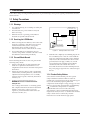
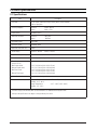
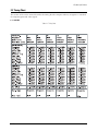
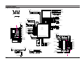
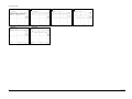
TFT-LCD MONITOR
GH15DS
SERVICE
Manual
TFT-LCD MONITOR
CONTENTS
1. Precautions
2. Product Specifications
3. Disassembly & Reassembly
4. Troubleshooting
5. Exploded View & Parts List
6. Electrical Parts List
7. Block Diagram
8. Wiring Diagram
9. Schematic Diagrams
10. Panel Description
1 Precautions
Follow these safety, servicing and ESD precautions to prevent damage and to protect against potential hazards such as
electrical shock.
1-1 Safety Precautions
1-1-1 Warnings
1.
For continued safety, do not attempt to modify the
circuit board.
2.
Disconnect the AC power and DC Power Jack
before servicing.
3.
When the chassis is operating, semiconductor
heatsinks are potential shock hazards.
(READING SHOULD
NOT BE ABOVE 0.5mA)
TEST ALL
EXPOSED METAL
SURFACES
1-1-2 Servicing the LCD Monitor
1.
2.
1-1-3 Fire and Shock Hazard
Before returning the monitor to the user, perform the
following safety checks:
1.
Inspect each lead dress to make certain that the
leads are not pinched or that hardware is not
lodged between the chassis and other metal parts in
the monitor.
2.
Inspect all protective devices such as nonmetallic
control knobs, insulating materials, cabinet backs,
adjustment and compartment covers or shields,
isolation resistor-capacitor networks, mechanical
insulators, etc.
3.
2-WIRE CORD
When servicing the LCD Monitor, remove the static
charge by connecting a 10k ohm resistor in series
with an insulated wire (such as a test probe)
between the chassis and the anode lead.
(Disconnect the AC line cord from the AC outlet.)
It is essential that service technicians have an
accurate voltage meter available at all times. Check
the calibration of this meter periodically.
Leakage Current Hot Check (Figure 1-1):
WARNING: Do not use an isolation transformer
during this test.
Use a leakage current tester or a metering system
that complies with American National Standards
Institute (ANSI C101.1, Leakage Current for
Appliances), and Underwriters Laboratories (UL
Publication UL1410, 59.7).
GH15DS
LEAKAGE
CURRENT
TESTER
DEVICE
UNDER
TEST
*ALSO TEST WITH
PLUG REVERSED
(USING AC ADAPTER
PLUG AS REQUIRED)
EARTH
GROUND
Figure 1-1. Leakage Current Test Circuit
4.
With the unit completely reassembled, plug the AC
line cord directly into a 120V AC outlet. With the
unit’s AC switch first in the ON position and then
OFF, measure the current between a known earth
ground (metal water pipe, conduit, etc.) and all
exposed metal parts, including: metal cabinets,
screwheads and control shafts. The current
measured should not exceed 0.5 milliamp. Reverse
the power-plug prongs in the AC outlet and repeat
the test.
1-1-4 Product Safety Notices
Some electrical and mechanical parts have special
safety-related characteristics which are often not
evident from visual inspection. The protection they give
may not be obtained by replacing them with
components rated for higher voltage, wattage, etc. Parts
that have special safety characteristics are identified by
! on schematics and parts lists. A substitute
replacement that does not have the same safety
characteristics as the recommended replacement part
might create shock, fire and / or other hazards. Product
safety is under review continuously and new
instructions are issued whenever appropriate.
1-1
1 Precautions
1-2 Servicing Precautions
WARNING:
An electrolytic capacitor installed with the wrong polarity might explode.
Caution:
Before servicing units covered by this service manual, read and follow the Safety Precautions
section of this manual.
Note:
If unforeseen circumstances create conflict between the following servicing precautions and any of the
safety precautions, always follow the safety precautions.
1-2-1 General Servicing Precautions
1.
2.
3.
Always unplug the unit’s AC power cord from the
AC power source and disconnect the DC Power
Jack before attempting to:
(a) remove or reinstall any component or assembly,
(b) disconnect PCB plugs or connectors, (c) connect
a test component in parallel with an electrolytic
capacitor.
Some components are raised above the printed
circuit board for safety. An insulation tube or tape
is sometimes used. The internal wiring is
sometimes clamped to prevent contact with
thermally hot components. Reinstall all such
elements to their original position.
4.
Check the insulation between the blades of the AC
plug and accessible conductive parts (examples:
metal panels, input terminals and earphone jacks).
5.
Insulation Checking Procedure: Disconnect the
power cord from the AC source and turn the power
switch ON. Connect an insulation resistance meter
(500 V) to the blades of the AC plug.
The insulation resistance between each blade of the
AC plug and accessible conductive parts (see
above) should be greater than 1 megohm.
6.
After servicing, always check that the screws,
components and wiring have been correctly
reinstalled. Make sure that the area around the
serviced part has not been damaged.
Always connect a test instrument’s ground lead to
the instrument chassis ground before connecting
the positive lead; always remove the instrument’s
ground lead last.
1-3 Electrostatically Sensitive Devices (ESD) Precautions
Some semiconductor (solid state) devices can be easily damaged by static electricity. Such components are commonly
called Electrostatically Sensitive Devices (ESD). Examples of typical ESD devices are integrated circuits and some fieldeffect transistors. The following techniques will reduce the incidence of component damage caused by static electricity.
1.
Immediately before handling any semiconductor
components or assemblies, drain the electrostatic
charge from your body by touching a known earth
ground. Alternatively, wear a discharging wriststrap device. To avoid a shock hazard, be sure to
remove the wrist strap before applying power to
the monitor.
6.
Do not remove a replacement ESD from its
protective package until you are ready to install it.
Most replacement ESDs are packaged with leads
that are electrically shorted together by conductive
foam, aluminum foil or other conductive materials.
7.
2.
After removing an ESD-equipped assembly, place it
on a conductive surface such as aluminum foil to
prevent accumulation of an electrostatic charge.
Immediately before removing the protective
material from the leads of a replacement ESD,
touch the protective material to the chassis or
circuit assembly into which the device will be
installed.
3.
Do not use freon-propelled chemicals. These can
generate electrical charges sufficient to damage
ESDs.
Caution: Be sure no power is applied to the
chassis or circuit and observe all
other safety precautions.
4.
Use only a grounded-tip soldering iron to solder or
desolder ESDs.
5.
Use only an anti-static solder removal device. Some
solder removal devices not classified as “anti-static”
can generate electrical charges sufficient to damage
ESDs.
1-2
8.
Minimize body motions when handling
unpackaged replacement ESDs. Motions such as
brushing clothes together, or lifting your foot from
a carpeted floor can generate enough static
electricity to damage an ESD.
GH15DS
2 Product Specifications
2-1 Specifications
Item
Description
LCD Panel
TFT-LCD panel, RGB vertical stripe, normaly white,15-Inch viewable,
0.297 mm pixel pitch
Scanning Frequency
Horizontal
Vertical
Display Colors
16.2 Million colors
Maximum Resolution
Horizontal
Vertical
Input Video Signal
VESA TMDS
Input Sync Signal
Encoded by TMDS
Maximum Pixel Clock rate
80 MHz
Active Display
Horizontal : 304 mm
:
:
:
:
30 kHz ~ 60 kHz
56 Hz ~ 75 Hz
1024 Pixels
768 Pixels
Vertical : 228 mm
AC power voltage & Frequency AC 90 ~ 260 Volts, 60/50 Hz ± 3 Hz
Power Consumption
Dimensions
Unit (W x D x H)
With Simple Stand
Without Simple stand
With Pivot Stand
On : 30 W (max) / Saving : 3W (max) / Switch - off : 1W (max)
Without Pivot Stand
15.4 x 15.1 x 6.8 Inches (391.4 x 383.6 x 173 mm)
15.4 x 11.5 x 2.5 Inches (391.4 x 292.8 x 64.0 mm)
15.4 x 15.1 x 6.8 Inches (391.4 x 383.6 x 173 mm)
15.4 x 17.1 x 6.8 Inches (391.4 x 433.6 x 173 mm)
15.4 x 11.5 x 2.5 Inches (391.4 x 292.8 x 64.0 mm)
Weight (Net/Gross)
4.2 kg (9.3 lbs) / 5.2 kg (11.5 lbs)
Environmental Considerations
Operating Temperature :
Humidity : 10 % ~ 80 %
Storage Temperature :
Humidity : 5 % ~ 95 %
50°F ~ 104°F (10°C ~ 40°C)
-3.2°F ~ 140°F (-20°C ~ 60°C)
•GH15DS comply with SWEDAC (MPR II) recommendations for reduced electromagnetic fields.
•Designs and specifications are subject to change without prior notice.
GH15DS
2-1
2 Product Specifications
2-2 DVI Signal Pin Assignments - Main Pin Field (GH15DS)
Pin
2-2
Signal Assignment
Pin
Signal Assignment
Pin
Signal Assignment
1
T.M.D.S. Data2-
9
T.M.D.S. Data1-
17
T.M.D.S. Data0-
2
T.M.D.S. Data2+
10
T.M.D.S. Data1+
18
T.M.D.S. Data0+
3
T.M.D.S. Data2 Return
11
T.M.D.S. Data1 Return
19
T.M.D.S. Data0 Return
4
NC
12
NC
20
NC
5
NC
13
NC
21
NC
6
DDC Clock
14
+5V Power
22
T.M.D.S. Clock Return
7
DDC Data
15
Ground (Self-Raster)
23
T.M.D.S. Clock+
8
NC
16
Hot Plug Detect (+5V)
24
T.M.D.S. Clock-
GH15DS
2 Product Specifications
2-3 Timing Chart
This section of the service manual describes the timing that the computer industry recognizes as standard
for computer-generated video signals.
2-3-1. GH15DS
Table 2-1. Timing Chart
GH15DS
2-3
2 Product Specifications
Table 2-2. Timing Chart
2-4
GH15DS
3 Disassembly and Reassembly
This section of the service manual describes the disassembly and reassembly procedures for the
GH15DS monitor.
WARNING: This monitor contains electrostatically sensitive devices. Use with caution when
handling these components.
3-1 Disassembly
Cautions:1. Disconnect the monitor from the power source before disassembly.
2. Follow these directions carefully; never use metal instruments to pry apart the cabinet.
3-1-1 Removing the Stand
3-1-3 Standard Stand Disassembly
1. Remove 4 screws in the hinge area.
1. Remove 2 screws from the Stand front.
2. Disconnect Power Cord and Signal Cable.
2. Remove 7 screws from the Stand Bottom.
3. Pry it off the back of the monitor.
3. Remove Stand Rear from the Stand assembly.
4. Remove 5 screws from the Stand assembly.
3-1-2 Main Body Disassembly
5. Remove the Neck front from the Stand
assembly.
1. Remove 2 screws on the two corner of the
Rear Cover.
6. Remove 2 screws from the Stand assembly.
2. Remove Rear Cover from the Front Cover.
3. Remove 4 screws on the Shield and remove
the shield.
7. Remove Neck Rear from the Stand assembly.
8. Remove 4 screws from the Stand assembly.
4. Disconnect Inverter wire, Function PCB wire
and Interface wire.
Remove 3 screws on the Main PCB and
remove 2 screws on the D sub shield.
5. Remove 3 screws on the power PCB and
remove 2 screws on the Inverter PCB.
6. Remove the Main PCB Assembly.
7. Remove 3 screws on the Function PCB from
locking area of Function knob and remove
Function PCB.
GH15DS
3-1
3 Disassembly and Reassembly
3-2 Replacement Order of Lamp Assemblies (GH15DS : Samsung Panel)
1. After confirm there is nothing
on the disk
Turn the LCD module over
and put it on a flat desk set to
the ground.
2. Push down the stopper and
slide the lamp unit.
3. Please take out the lamp
unit from the LCD
module.
3-2
GH15DS
3 Disassembly and Reassembly
4. Please fix the new lamp
units on the LCD module :
opposite process 2 and 3
*
Replacement of lamp unit should be done at the power off state and recommanded clean
bench condition.
3-3 Reassembly
Reassembly procedures are in the reverse order of Disassembly procedures.
GH15DS
3-3
3 Disassembly and Reassembly
Memo
3-4
GH15DS
4 Troubleshooting
Notes: 1. Before troubleshooting, setup the PC’s display as below.
• Resolution: 1024 x 768
• H-frequency: 48 kHz
• V-frequency: 60 Hz
2. If no picture appears, make sure the power cord is correctly connected.
3. Check the following circuits.
• No raster appears: Main PCB
• 12V develop but no screen: Main PCB
• 12V does not develop: Main PCB
4. If you push and hold the EXIT button for more than 5 seconds, the monitor automatically turns back
to the factory preset(GH15DS).
4-1 Power
Does proper DC 12 V
appear at CN100?
No
Check Power Adaptor.
Yes
Does proper DC 5 V appear at
output Pin of IC100?
No
Check IC100 and related circuit.
Yes
Does proper 3.3 V - signals
appear at output Pin of IC103?
No
Check IC103 and related circuit.
Yes
Does proper 3.3 V - signals
appear at Pin 7 of CN100?
No
Check CN100-7 and related circuit.
Yes
Does proper 3.3 V - signals
appear at R300?
No
Check IC301 and related circuit.
Yes
Check IC101, IC102, IC601, IC401
and related circuit.
GH15DS
4-1
4 Troubleshooting
4-2 Video
Power indicator is green?
Do the input signals
appear at D201~D208?
No
1
2
Yes
Check X301.
No
Yes
Check Pin 68 of IC301 and IC102.
Do the input signals appear at
pin 30, 31, 32 of IC401?
3
4
No
Check IC301.
5
Yes
Do the output signals appear
at pin 40 of IC401?
No
Check IC401.
6
Yes
Replace LCD panel.
4-2
GH15DS
4 Troubleshooting
WAVEFORMS
1 D201
2 D208
3 IC401 #30
4 IC401 #31
5 IC401 #32
6 IC401 #40
GH15DS
4-3
4 Troubleshooting
Memo
4-4
GH15DS
5 Exploded View and Parts List
GH15DS
5-1
5 Exploded View & Parts List
Memo
5-2
GH15DS
6 Electrical Parts List
6-1 Main PCB Part
Loc. No.
Code No.
Description
CIS
CIS
CIS
CIS
CIS
CIS
CN100
CN201
CN601
DVI
IC601
SOCK_IC601
C102
C103
C104
C105
C106
C107
C108
C112
C113
C114
C115
C201
C202
C301
C302
C303
C304
C307
C308
C309
C310
C311
C312
C313
C314
C315
C316
C317
C318
C319
C320
C321
C322
C323
C325
C326
C327
BN44-00053A
BN72-00209A
BN75-00176B
BN70-00204B
BN71-00024A
BN46-00008K
3711-004853
3701-001173
3711-001465
BN60-00001A
0903-001143
3704-001071
2402-000176
2203-005005
2203-005005
2402-001042
2203-005005
2203-005005
2203-005005
2203-005005
2203-005005
2203-005005
2203-005005
2402-000176
2203-005005
2203-005005
2402-001042
2203-005005
2402-001042
2402-000135
2203-005005
2203-005005
2203-005005
2203-005005
2203-005005
2203-005005
2203-005005
2203-005005
2203-000384
2203-000384
2203-000384
2203-000384
2203-005005
2203-005005
2203-005005
2402-000135
2402-000135
2203-005005
2203-005005
ADAPTOR
SUPPORT-POWER
UNIT-SHIELD/DSUB
SHIELD-D/SUB
EARTH-PLATE
MICOM-S/W,GOGH
CONNECTOR-HEADER
CONNECTOR-DSUB
CONNECTOR-HEADER
SCREW-CHASSIS
IC-MICROCONTROLLER
SOCKET-IC
C-AL,SMD
C-CERAMIC,CHIP
C-CERAMIC,CHIP
C-AL,SMD
C-CERAMIC,CHIP
C-CERAMIC,CHIP
C-CERAMIC,CHIP
C-CERAMIC,CHIP
C-CERAMIC,CHIP
C-CERAMIC,CHIP
C-CERAMIC,CHIP
C-AL,SMD
C-CERAMIC,CHIP
C-CERAMIC,CHIP
C-AL,SMD
C-CERAMIC,CHIP
C-AL,SMD
C-AL,SMD
C-CERAMIC,CHIP
C-CERAMIC,CHIP
C-CERAMIC,CHIP
C-CERAMIC,CHIP
C-CERAMIC,CHIP
C-CERAMIC,CHIP
C-CERAMIC,CHIP
C-CERAMIC,CHIP
C-CERAMIC,CHIP
C-CERAMIC,CHIP
C-CERAMIC,CHIP
C-CERAMIC,CHIP
C-CERAMIC,CHIP
C-CERAMIC,CHIP
C-CERAMIC,CHIP
C-AL,SMD
C-AL,SMD
C-CERAMIC,CHIP
C-CERAMIC,CHIP
GH15DS
Specification
DPA30L,150S,100-240VAC,47 - 63 HZ,12VDC/3.3VDC,2A/2A,-,30.6,AC-DC,-10~40C,-,GH15LS,ABS+PC,GR37,-,5V,-,-,GH15LS,-,SPTE T0.5,-,-,-,GH15DS,SPTE,-,T0.5,-,-,GH17LS,SUS,T0.15,-,-,GH15DS,-,-,-,-,-,BOX,7P,1R,2MM,ANGLE,SN,WHT
24P,3R,FEMALE,ANGLE,AUF
NOWALL,3P,1R,2.54mm,STRAIGHT,A
-,NI PLATING,-,11,HEX,HEX,-,UNC#4-40,NI PLT,88P6232,8BITBit,SDIP,42P,600MIL,12MHz,ST,CMOS,PLASTIC,5V,-,-40to+85C,464BYTE,32K
42P,DIP,SN,1.778mm
10uF,20%,16V,GP,TP,4.3x4.3x5.4
100nF,10%,16V,X7R,TP,1608
100nF,10%,16V,X7R,TP,1608
100uF,20%,16V,GP,TP,6.6x6.6x5.4mm
100nF,10%,16V,X7R,TP,1608
100nF,10%,16V,X7R,TP,1608
100nF,10%,16V,X7R,TP,1608
100nF,10%,16V,X7R,TP,1608
100nF,10%,16V,X7R,TP,1608
100nF,10%,16V,X7R,TP,1608
100nF,10%,16V,X7R,TP,1608
10uF,20%,16V,GP,TP,4.3x4.3x5.4
100nF,10%,16V,X7R,TP,1608
100nF,10%,16V,X7R,TP,1608
100uF,20%,16V,GP,TP,6.6x6.6x5.4mm
100nF,10%,16V,X7R,TP,1608
100uF,20%,16V,GP,TP,6.6x6.6x5.4mm
22uF,20%,16V,GP,TP,5.3x5.3x5.4
100nF,10%,16V,X7R,TP,1608
100nF,10%,16V,X7R,TP,1608
100nF,10%,16V,X7R,TP,1608
100nF,10%,16V,X7R,TP,1608
100nF,10%,16V,X7R,TP,1608
100nF,10%,16V,X7R,TP,1608
100nF,10%,16V,X7R,TP,1608
100nF,10%,16V,X7R,TP,1608
0.015nF,5%,50V,NP0,TP,1608
0.015nF,5%,50V,NP0,TP,1608
0.015nF,5%,50V,NP0,TP,1608
0.015nF,5%,50V,NP0,TP,1608
100nF,10%,16V,X7R,TP,1608
100nF,10%,16V,X7R,TP,1608
100nF,10%,16V,X7R,TP,1608
22uF,20%,16V,GP,TP,5.3x5.3x5.4
22uF,20%,16V,GP,TP,5.3x5.3x5.4
100nF,10%,16V,X7R,TP,1608
100nF,10%,16V,X7R,TP,1608
Remarks
SNA
SNA
SNA
SNA
SNA
SNA
SNA
SNA
6-1
6 Electrical Parts List
Loc. No.
C328
C329
C330
C331
C332
C333
C334
C335
C336
C402
C403
C404
C405
C413
C414
C415
C600
C601
C602
C603
C604
C605
C606
C610
C611
C612
C613
C614
CA301
CA302
CA303
CA304
CA305
CA306
CN101
CN402
CN600
D201
D202
D203
D204
D205
D206
D207
D208
D209
D210
FT301
FT302
FT303
FT402
6-2
Code No.
2203-005005
2203-005005
2203-005005
2402-000135
2203-005005
2203-005005
2203-005005
2203-000280
2203-000280
2203-000440
2203-000440
2203-000440
2203-000440
2203-005005
2402-001042
2402-000176
2203-005005
2402-001042
2203-000626
2203-000626
2402-000176
2203-005005
2203-005005
2203-005005
2203-005005
2203-005005
2203-005005
2203-005005
2503-001019
2503-001019
2503-001019
2503-001019
2503-001019
2503-001019
3711-000556
3711-003161
3711-002049
0401-001056
0401-001056
0401-001056
0401-001056
0401-001056
0401-001056
0401-001056
0401-001056
0401-001056
0401-001056
2901-001114
2901-001114
2901-001114
2901-001114
Description
C-CERAMIC,CHIP
C-CERAMIC,CHIP
C-CERAMIC,CHIP
C-AL,SMD
C-CERAMIC,CHIP
C-CERAMIC,CHIP
C-CERAMIC,CHIP
C-CERAMIC,CHIP
C-CERAMIC,CHIP
C-CERAMIC,CHIP
C-CERAMIC,CHIP
C-CERAMIC,CHIP
C-CERAMIC,CHIP
C-CERAMIC,CHIP
C-AL,SMD
C-AL,SMD
C-CERAMIC,CHIP
C-AL,SMD
C-CERAMIC,CHIP
C-CERAMIC,CHIP
C-AL,SMD
C-CERAMIC,CHIP
C-CERAMIC,CHIP
C-CERAMIC,CHIP
C-CERAMIC,CHIP
C-CERAMIC,CHIP
C-CERAMIC,CHIP
C-CERAMIC,CHIP
C-NETWORK
C-NETWORK
C-NETWORK
C-NETWORK
C-NETWORK
C-NETWORK
CONNECTOR-HEADER
CONNECTOR-HEADER
CONNECTOR-HEADER
DIODE-SWITCHING
DIODE-SWITCHING
DIODE-SWITCHING
DIODE-SWITCHING
DIODE-SWITCHING
DIODE-SWITCHING
DIODE-SWITCHING
DIODE-SWITCHING
DIODE-SWITCHING
DIODE-SWITCHING
FILTER-EMI SMD
FILTER-EMI SMD
FILTER-EMI SMD
FILTER-EMI SMD
Specification
100nF,10%,16V,X7R,TP,1608
100nF,10%,16V,X7R,TP,1608
100nF,10%,16V,X7R,TP,1608
22uF,20%,16V,GP,TP,5.3x5.3x5.4
100nF,10%,16V,X7R,TP,1608
100nF,10%,16V,X7R,TP,1608
100nF,10%,16V,X7R,TP,1608
0.01nF,0.5pF,50V,NP0,TP,1608
0.01nF,0.5pF,50V,NP0,TP,1608
1nF,10%,50V,X7R,TP,1608,1nF,10%,50V,X7R,TP,1608,1nF,10%,50V,X7R,TP,1608,1nF,10%,50V,X7R,TP,1608,100nF,10%,16V,X7R,TP,1608
100uF,20%,16V,GP,TP,6.6x6.6x5.4mm
10uF,20%,16V,GP,TP,4.3x4.3x5.4
100nF,10%,16V,X7R,TP,1608
100uF,20%,16V,GP,TP,6.6x6.6x5.4mm
0.022nF,5%,50V,NP0,TP,1608
0.022nF,5%,50V,NP0,TP,1608
10uF,20%,16V,GP,TP,4.3x4.3x5.4
100nF,10%,16V,X7R,TP,1608
100nF,10%,16V,X7R,TP,1608
100nF,10%,16V,X7R,TP,1608
100nF,10%,16V,X7R,TP,1608
100nF,10%,16V,X7R,TP,1608
100nF,10%,16V,X7R,TP,1608
100nF,10%,16V,X7R,TP,1608
33PFX4,10%,50V,CHIP
33PFX4,10%,50V,CHIP
33PFX4,10%,50V,CHIP
33PFX4,10%,50V,CHIP
33PFX4,10%,50V,CHIP
33PFX4,10%,50V,CHIP
BOX,12P,1R,1.25mm,SMD-A,SN
BOX,20P,1R,1.25mm,ANGLE,SN
BOX,6P,1R,1.25mm,SMD-A,SN
MMBD4148SE,75V,200MA,SOT-23,TP
MMBD4148SE,75V,200MA,SOT-23,TP
MMBD4148SE,75V,200MA,SOT-23,TP
MMBD4148SE,75V,200MA,SOT-23,TP
MMBD4148SE,75V,200MA,SOT-23,TP
MMBD4148SE,75V,200MA,SOT-23,TP
MMBD4148SE,75V,200MA,SOT-23,TP
MMBD4148SE,75V,200MA,SOT-23,TP
MMBD4148SE,75V,200MA,SOT-23,TP
MMBD4148SE,75V,200MA,SOT-23,TP
25VDC,2.0ADC,-,100nF,3.2x1.6x1
25VDC,2.0ADC,-,100nF,3.2x1.6x1
25VDC,2.0ADC,-,100nF,3.2x1.6x1
25VDC,2.0ADC,-,100nF,3.2x1.6x1
Remarks
SNA
SNA
SNA
GH15DS
6 Electrical Parts List
Loc. No.
FT407
IC100
IC103
IC201
IC301
IC401
IC603
L100
L101
L102
L201
L303
L304
L401
L402
L602
L603
L604
L605
L606
MP1.0
Q101
Q102
Q103
Q600
Q601
Q602
Q603
Q605
Q606
R100
R101
R102
R103
R104
R105
R106
R107
R108
R109
R110
R111
R112
R113
R114
R201
R202
R203
R204
R205
R300
GH15DS
Code No.
Description
2901-001114
1203-001488
1203-001293
1103-000129
1003-001374
1205-001740
1103-000129
2703-001334
2703-001334
2703-001334
2703-001334
2703-001334
2703-001334
2703-001334
2703-001334
2703-001334
2703-001334
2703-001334
2703-001334
2703-001334
BN41-00093A
0501-002080
0501-002080
0501-002080
0501-002080
0501-002080
0501-002080
0501-002080
0501-002080
0501-002080
2007-000074
2007-000070
2007-000070
2007-000102
2007-000090
2007-000102
2007-000090
2007-000102
2007-000090
2007-000070
2007-000070
2007-000070
2007-000070
2007-000070
2007-000070
2007-000078
2007-000084
2007-000084
2007-000074
2007-000074
2007-000070
FILTER-EMI SMD
IC-POSI.FIXED REG.
IC-POSI.FIXED REG.
IC-EEPROM
IC-LCD CONTROLLER
IC-TRANSMITTER
IC-EEPROM
INDUCTOR-SMD
INDUCTOR-SMD
INDUCTOR-SMD
INDUCTOR-SMD
INDUCTOR-SMD
INDUCTOR-SMD
INDUCTOR-SMD
INDUCTOR-SMD
INDUCTOR-SMD
INDUCTOR-SMD
INDUCTOR-SMD
INDUCTOR-SMD
INDUCTOR-SMD
PCB MAIN
TR-SMALL SIGNAL
TR-SMALL SIGNAL
TR-SMALL SIGNAL
TR-SMALL SIGNAL
TR-SMALL SIGNAL
TR-SMALL SIGNAL
TR-SMALL SIGNAL
TR-SMALL SIGNAL
TR-SMALL SIGNAL
R-CHIP
R-CHIP
R-CHIP
R-CHIP
R-CHIP
R-CHIP
R-CHIP
R-CHIP
R-CHIP
R-CHIP
R-CHIP
R-CHIP
R-CHIP
R-CHIP
R-CHIP
R-CHIP
R-CHIP
R-CHIP
R-CHIP
R-CHIP
R-CHIP
Specification
Remarks
25VDC,2.0ADC,-,100nF,3.2x1.6x1
7805,T0-252,3P,-,PLASTIC,4.8/5
033,T0-252,3P,6.5MIL,PLASTIC,3
24C02,256x8BIT,SOP,8P,150MIL,1
GM3020,LQFP,128P,551MIL,SINGLE,-,-,PLASTIC,3.47V,0TO+70C,-,-,DS90C385,TSSOP,56P,240MIL,PLASTIC,4V,1.63W,-10 TO +70C,ST,FPD LINK-85MHZ(LVDS)
24C02,256x8BIT,SOP,8P,150MIL,1
1.5uH,10%,2x1.25x0.85mm
1.5uH,10%,2x1.25x0.85mm
1.5uH,10%,2x1.25x0.85mm
1.5uH,10%,2x1.25x0.85mm
1.5uH,10%,2x1.25x0.85mm
1.5uH,10%,2x1.25x0.85mm
1.5uH,10%,2x1.25x0.85mm
1.5uH,10%,2x1.25x0.85mm
1.5uH,10%,2x1.25x0.85mm
1.5uH,10%,2x1.25x0.85mm
1.5uH,10%,2x1.25x0.85mm
1.5uH,10%,2x1.25x0.85mm
1.5uH,10%,2x1.25x0.85mm
S/M150DS,FR4,2L,-,-,120*110*1.6,GH15D,-,-,2SC2412K,NPN,200mW,SC-59,TP,120-270
2SC2412K,NPN,200mW,SC-59,TP,120-270
2SC2412K,NPN,200mW,SC-59,TP,120-270
2SC2412K,NPN,200mW,SC-59,TP,120-270
2SC2412K,NPN,200mW,SC-59,TP,120-270
2SC2412K,NPN,200mW,SC-59,TP,120-270
2SC2412K,NPN,200mW,SC-59,TP,120-270
2SC2412K,NPN,200mW,SC-59,TP,120-270
2SC2412K,NPN,200mW,SC-59,TP,120-270
100ohm,5%,1/16W,DA,TP,1608
0ohm,5%,1/16W,DA,TP,1608
0ohm,5%,1/16W,DA,TP,1608
100Kohm,5%,1/16W,DA,TP,1608
10KOHM,5%,1/16W,DA,TP,1608
100Kohm,5%,1/16W,DA,TP,1608
10KOHM,5%,1/16W,DA,TP,1608
100Kohm,5%,1/16W,DA,TP,1608
10KOHM,5%,1/16W,DA,TP,1608
0ohm,5%,1/16W,DA,TP,1608
0ohm,5%,1/16W,DA,TP,1608
0ohm,5%,1/16W,DA,TP,1608
0ohm,5%,1/16W,DA,TP,1608
0ohm,5%,1/16W,DA,TP,1608
0ohm,5%,1/16W,DA,TP,1608
1Kohm,5%,1/16W,DA,TP,1608
4.7Kohm,5%,1/16W,DA,TP,1608
4.7Kohm,5%,1/16W,DA,TP,1608
100ohm,5%,1/16W,DA,TP,1608
100ohm,5%,1/16W,DA,TP,1608
0ohm,5%,1/16W,DA,TP,1608
6-3
6 Electrical Parts List
Loc. No.
R301
R302
R303
R304
R309
R310
R311
R312
R313
R314
R315
R316
R317
R318
R322
R323
R324
R327
R329
R330
R331
R332
R401
R402
R403
R600
R601
R602
R606
R608
R609
R610
R611
R612
R613
R614
R615
R616
R618
R619
R620
R621
R622
R623
R624
R625
R626
R627
R628
R629
R630
6-4
Code No.
2007-000070
2007-000071
2007-000071
2007-000071
2007-000071
2007-000078
2007-000309
2007-000309
2007-000309
2007-000309
2007-000309
2007-000309
2007-000309
2007-000309
2007-000074
2007-000074
2007-000074
2007-000074
2007-000078
2007-000070
2007-000070
2007-000109
2007-000074
2007-000074
2007-000074
2007-000070
2007-000078
2007-000084
2007-000084
2007-000084
2007-000084
2007-000084
2007-000084
2007-000074
2007-000074
2007-000109
2007-000084
2007-000084
2007-000084
2007-000084
2007-000084
2007-000084
2007-000084
2007-000074
2007-000078
2007-000090
2007-000074
2007-000074
2007-000074
2007-000090
2007-000102
Description
R-CHIP
R-CHIP
R-CHIP
R-CHIP
R-CHIP
R-CHIP
R-CHIP
R-CHIP
R-CHIP
R-CHIP
R-CHIP
R-CHIP
R-CHIP
R-CHIP
R-CHIP
R-CHIP
R-CHIP
R-CHIP
R-CHIP
R-CHIP
R-CHIP
R-CHIP
R-CHIP
R-CHIP
R-CHIP
R-CHIP
R-CHIP
R-CHIP
R-CHIP
R-CHIP
R-CHIP
R-CHIP
R-CHIP
R-CHIP
R-CHIP
R-CHIP
R-CHIP
R-CHIP
R-CHIP
R-CHIP
R-CHIP
R-CHIP
R-CHIP
R-CHIP
R-CHIP
R-CHIP
R-CHIP
R-CHIP
R-CHIP
R-CHIP
R-CHIP
Specification
Remarks
0ohm,5%,1/16W,DA,TP,1608
22ohm,5%,1/16W,DA,TP,1608
22ohm,5%,1/16W,DA,TP,1608
22ohm,5%,1/16W,DA,TP,1608
22ohm,5%,1/16W,DA,TP,1608
1Kohm,5%,1/16W,DA,TP,1608
10ohm,5%,1/16W,DA,TP,1608
10ohm,5%,1/16W,DA,TP,1608
10ohm,5%,1/16W,DA,TP,1608
10ohm,5%,1/16W,DA,TP,1608
10ohm,5%,1/16W,DA,TP,1608
10ohm,5%,1/16W,DA,TP,1608
10ohm,5%,1/16W,DA,TP,1608
10ohm,5%,1/16W,DA,TP,1608
100ohm,5%,1/16W,DA,TP,1608
100ohm,5%,1/16W,DA,TP,1608
100ohm,5%,1/16W,DA,TP,1608
100ohm,5%,1/16W,DA,TP,1608
1Kohm,5%,1/16W,DA,TP,1608
0ohm,5%,1/16W,DA,TP,1608
0ohm,5%,1/16W,DA,TP,1608
1Mohm,5%,1/16W,DA,TP,1608
100ohm,5%,1/16W,DA,TP,1608
100ohm,5%,1/16W,DA,TP,1608
100ohm,5%,1/16W,DA,TP,1608
0ohm,5%,1/16W,DA,TP,1608
1Kohm,5%,1/16W,DA,TP,1608
4.7Kohm,5%,1/16W,DA,TP,1608
4.7Kohm,5%,1/16W,DA,TP,1608
4.7Kohm,5%,1/16W,DA,TP,1608
4.7Kohm,5%,1/16W,DA,TP,1608
4.7Kohm,5%,1/16W,DA,TP,1608
4.7Kohm,5%,1/16W,DA,TP,1608
100ohm,5%,1/16W,DA,TP,1608
100ohm,5%,1/16W,DA,TP,1608
1Mohm,5%,1/16W,DA,TP,1608
4.7Kohm,5%,1/16W,DA,TP,1608
4.7Kohm,5%,1/16W,DA,TP,1608
4.7Kohm,5%,1/16W,DA,TP,1608
4.7Kohm,5%,1/16W,DA,TP,1608
4.7Kohm,5%,1/16W,DA,TP,1608
4.7Kohm,5%,1/16W,DA,TP,1608
4.7Kohm,5%,1/16W,DA,TP,1608
100ohm,5%,1/16W,DA,TP,1608
1Kohm,5%,1/16W,DA,TP,1608
10KOHM,5%,1/16W,DA,TP,1608
100ohm,5%,1/16W,DA,TP,1608
100ohm,5%,1/16W,DA,TP,1608
100ohm,5%,1/16W,DA,TP,1608
10KOHM,5%,1/16W,DA,TP,1608
100Kohm,5%,1/16W,DA,TP,1608
GH15DS
6 Electrical Parts List
Loc. No.
R631
R632
R633
R634
R635
R636
R637
R638
R639
R640
R641
R642
R866
R867
R868
RA301
RA302
RA303
RA304
RA305
RA306
X301
X601
ZD201
ZD202
ZD203
ZD204
ZD205
Code No.
2007-000090
2007-000074
2007-000074
2007-001002
2007-001002
2007-000090
2007-000090
2007-000090
2007-000090
2007-000090
2007-000074
2007-000078
2007-000074
2007-000074
2007-000074
2011-000002
2011-000002
2011-000002
2011-000002
2011-000002
2011-000002
2801-004004
2801-003773
0403-000579
0403-000579
0403-000579
0403-000579
0403-000579
Description
R-CHIP
R-CHIP
R-CHIP
R-CHIP
R-CHIP
R-CHIP
R-CHIP
R-CHIP
R-CHIP
R-CHIP
R-CHIP
R-CHIP
R-CHIP
R-CHIP
R-CHIP
R-NETWORK
R-NETWORK
R-NETWORK
R-NETWORK
R-NETWORK
R-NETWORK
CRYSTAL-SMD
CRYSTAL-SMD
DIODE-ZENER
DIODE-ZENER
DIODE-ZENER
DIODE-ZENER
DIODE-ZENER
Specification
Remarks
10KOHM,5%,1/16W,DA,TP,1608
100ohm,5%,1/16W,DA,TP,1608
100ohm,5%,1/16W,DA,TP,1608
510ohm,5%,1/16W,DA,TP,1608
510ohm,5%,1/16W,DA,TP,1608
10KOHM,5%,1/16W,DA,TP,1608
10KOHM,5%,1/16W,DA,TP,1608
10KOHM,5%,1/16W,DA,TP,1608
10KOHM,5%,1/16W,DA,TP,1608
10KOHM,5%,1/16W,DA,TP,1608
100ohm,5%,1/16W,DA,TP,1608
1Kohm,5%,1/16W,DA,TP,1608
100ohm,5%,1/16W,DA,TP,1608
100ohm,5%,1/16W,DA,TP,1608
100ohm,5%,1/16W,DA,TP,1608
22ohm,5%,63mW,L,CHIP,8P,TP
22ohm,5%,63mW,L,CHIP,8P,TP
22ohm,5%,63mW,L,CHIP,8P,TP
22ohm,5%,63mW,L,CHIP,8P,TP
22ohm,5%,63mW,L,CHIP,8P,TP
22ohm,5%,63mW,L,CHIP,8P,TP
20.25MHz,20ppm,28-AAN,13pF,25ohm,TP
12MHZ,30PPM,28-AAN,20PF,50OHM,TP
BZX84C5V1,5.1V,5%,200mW,SOT-23
BZX84C5V1,5.1V,5%,200mW,SOT-23
BZX84C5V1,5.1V,5%,200mW,SOT-23
BZX84C5V1,5.1V,5%,200mW,SOT-23
BZX84C5V1,5.1V,5%,200mW,SOT-23
6-2 Others
Loc. No.
PANEL
MAIN PCB ASS’Y
SIGNAL CABLE
INVERTER HARNESS
LVDS HARNESS
POWER CORD(115V)
POWER CORD(230V)
INVERTER
GH15DS
Code No.
Description & Specification
BN07-00026A
BN94-00128A
BN39-00072A
BN39-00020A
BN39-00183A
BN39-00141A
BN39-00140A
BN44-00056A
LCD-DISPLAY;LTM150XH-L01,CZB,8BIT,333.6*254.76*12.5
ASSY PCB-SN;GH15DS
CBF SIGNAL;DET,2000MM,24P/24P,IVORY,-,DVI
CBF-HARNESS;12P/12P,170MM,BLU/YEL/WHT
LEAD CONNECTOR ASSY;UL2835#28,UL/CSA,20P,120MM
AC POWER CORD;125VAC,10A,1800,IVORY
AC POWER CORD;230VAC,250/10A,1.80M,3PIN EURO STRAIGH,IVORY
INVERTER;GOGH,SIC1542,48KHZ,12VDC,37*140*16,4LAMP
Remarks
6-5
6 Electrical Parts List
Memo
6-6
GH15DS
7 Block Diagram
GH15DS
7-1
7 Block Diagrams
Memo
7-2
GH15DS
GH15DS
GND
Rx2–
Rx2+
GND
NC
NC
DVI_CLK
DVI_DTA
NC
Rx1–
Rx1+
GND
NC
1
2
3
1
2
3
4
5
6
7
8
9
10
11
12
13
14
15
14
17
18
19
20
21
22
23
24
CN101
1
2
3
4
5
6
7
CN1
+12V
+12V_INV
GND
GND
GND
PWR_OFF
3.3V
1
2
3
4
5
6
7
1
2
3
4
5
6
7
8
9
10
NC
GND
Tx3A+
Tx3AGND
TxCA+
TxCAGND
Tx2A+
Tx2A-
NC
BRT_CTL_INV
NC
BL_ON
NC
GND
11
12
13
14
15
16
17
18
19
20
7
8
9
10
11
12
+12V
+12V_INV
GND
GND
GND
PWR_OFF
3.3V
GND
LCD_VCC
LCD_VCC
GND
Tx1A+
Tx1AGND
Tx0A+
Tx0AGND
+5V
GND
GND
+12V_INV
+12V_INV
+12V_INV
POWER PCB
NC
NC
GND
RxC+
RxC–
CN2
NC
DVI_+5V
DVI_GND
DVI_+5V
Rx0–
Rx0+
GND
1
2
3
4
5
6
8 Wiring Diagram
MAIN PCB
CN402
CN100
CN600
1
2
3
4
5
6
+3.3V
KEY_A
LED_R
KEY_B
LED_G
GND
CN201
8-1
8 Wiring Diagram
Memo
8-2
GH15DS
9 Schematic Diagrams
9-1 Main Part Schematic diagram
R309 22 1/16W
C312
100nF
16V
C313
100nF
16V
C314
100nF
16V
C315
100nF
16V
C310
100nF
16V
R303 22 1/16W
R304 22 1/16W
R331
0
1/16W
C316
15pF
50V
MO
CA301
C327
100nF
16V
Rx2+
Rx2-
R311
R312
10
10
1/16W
1/16W
2
3
Rx1+
1
Rx1+
Rx1+
Rx1-
R313
R314
10
10
1/16W
1/16W
Rx1-
1
3
Rx1
2
D204
MMBD4148SE
2
D205
MMBD4148SE
3
Rx0+
1
Rx0+
Rx0+
Rx0RxC+
RxC-
R315
R316
10
10
1/16W
1/16W
R317
R318
10
10
2
D206
MMBD4148SE
1/16W
1/16W
3
Rx0-
1
Rx0
2
D207
MMBD4148SE
RxC+
3
RxC+
1
R201
1K
1/16W
D208
MMBD4148SE
2
HPD
3.3V_RX
C331
22uF
FT303
16V
SGM32F1E104-2A
RxC-
1
1
RxC
A
B
C333
100nF
16V
MO
C332
100nF
16V
MO
DAR(0)
DAR(1)
DAR(2)
DAR(3)
DAR(4)
DAR(5)
DAR(7)
DAR(6)
DAR(7)
DAG(0)
CA303
DAG(1)
CA304
DAG(7:0)
DAG(5)
DAG(0)
DAG(1)
DAG(2)
DAG(4)
DAG(3)
DAG(3)
DAG(4)
DAG(2)
7 5 3 1 7 5 3 1
DAG(6)
DAG(7)
8 6 4 2 8 6 4 2
IC301
gm3020
C334
100nF
16V
MO
RA305
CA305
CA306
DAB(7:0)
DAB(0)
DAB(0)
DAB(1)
DAB(2)
DAB(2)
DAB(1)
DAB(3)
32
31
30
29
28
27
26
25
24
23
22
21
20
19
18
17
16
15
14
13
12
11
10
9
8
7
6
5
4
3
2
1
DAB(7)
PD15
PD16
PD17
RVSS2
RVDD2
PD18
PD19
PCLK
PDE
PD20
PD21
PD22
PD23
CVSS1
CVDD1
PD24
PD25
PVSS1
RVDD1
PD26
PD27
PD28
PD29
PD30
PD31
PD32
PD33
PD34
RVSS6
RVDD6
PD35
PD36
2
C
2
DVI_+5V
8 6 4 2 8 6 4 2
DAR(5)
DAB(3)
7 5 3 1 7 5 3 1
DAB(4)
DAB(5)
DAB(6)
8 6 4 2 8 6 4 2
DAB(7)
RA306
3.3V_LVDSTX
1
L401
1.5uH
FT402
SGM32F1E104-2A
2
A
B
C
3
C415
10uF
16V
97
98
99
100
101
102
103
104
105
106
107
108
109
110
111
112
113
114
115
116
117
118
119
120
121
122
123
124
125
126
127
128
D203
MMBD4148SE
65
OSD-DATA2
66
OSD-DATA3
67OSD-FSW
68
AVDD1
69
REXT
70 AGND1
71 VDD1
72
GND1
73
AGND2
74 RX2
75
RX276
AVDD2
77 VDD2
78
GND2
79
AGND3
80 RX1
81 RX182
AVDD3
83
VDD3
84 GND3
85
AGND4
86
RX0
87 RX088
AVDD4
89
RXC
90 RXC91
AVDD5
92
AGND5
93
AGND6
94 AVDD6
95
VBUFC
96
CLKOUT
5 3 1 7 5 3 1
3
C
B
2
3
Rx2-
1
Rx2
1
A
3
2
D202
MMBD4148SE
BZX84C5V1
7
R310
1K
1/16W
ZD201
Rx2+
1
Rx2+
3
1
9
17
2
10
18
3
11
19
4
12
20
5
13
21
6
14
22
7
15
23
8
16
24
25
26
27
28
29
30
31
32
2
D201
MMBD4148SE
CN201
tpcon32p_1
DAR(4)
RA304
2
C
3
1
DAR(3)
64
63
62
61
60
59
58
57
56
55
54
53
52
51
50
49
48
47
46
45
44
43
42
41
40
39
38
37
36
35
34
33
C326
100nF
16V
C330
100nF
16V
OSD_DATA1
OSD_DATA0
OSD_CLK
OSD_VREF
OSD_HREF
CVDD3
CVSS3
RVSS4
RVDD4
PPWR
PBIAS
PHS
PVS
PD0
PD1
PD2
PD3
PD4
PD5
PD6
PD7
PD8
RVSS3
RVDD3
CVDD2
CVSS2
PD9
PD10
PD11
PD12
PD13
PD14
B
A
C329
100nF
16V
PLL_RGNDA
PLL_RVDDA
XTAL
TCLK
DAC-DGNDA
DAC-DVDDA
PLL-DVDDA
PLL-DGNDA
DVDD
DVSS
HFS
HDATA
RESETn
IRQ
HCLK
STI_TM1
STI_TM2
PD47
PD46
PD45
RVSS5
RVDD5
CVDD4
CVSS4
PD44
PD43
PD42
PD41
PD40
PD39
PD38
PD37
1
C328
100nF
16V
7
R329
1K
1/16W
3.3V_RX
3.3V_RX
7 5 3 1 7 5 3 1
DAG(7)
C
3
C325
22uF
FT302
16V
SGM32F1E104-2A
DAR(2)
RA303
B2
A
DAR(7:0)
CA302
DAR(0)
DAR(1)
C319
15pF
50V
MO
RA302
8 6 4 2 8 6 4 2
1
C322
100nF
16V
MO
5 3 1 7 5 3 1
C323
22uF
FT301
16V
SGM32F1E104-2A
C321
100nF
16V
MO
8 6 4 2 8 6 4 2
C320
100nF
16V
MO
8 6 4 2 8 6 4 2
3.3V_RX
7 5 3 1 7 5 3 1
RA301
C318
15pF
50V
MO
C317
15pF
50V
MO
DAR(6)
R330
0
1/16W
DAB(4)
1.5uH
C309
100nF
16V
C301
100nF
16V
MO
C304
100uF
16.000
L304
C311
100nF
16V
DAG(5)
C303
100nF
16V
MO
C302
100uF
16.000
C308
100nF
16V
DAG(6)
L303
1.5uH
R302 22 1/16W
C307
22uF
16V
DAB(5)
R301
0
1/16W
DHS
DVS
DCLK
DDEN
3.3V_RX
3.3V_RX
DAB(6)
R300
0
1/16W
D3.3V
L402
C403
1nF
50V
MO
3
DVI_+5V
DVI_CLK
DVI_DAT
DVI_GND
DVI_CLK
DVI_DAT
DVI_GND
DAR(7:0)
IC401
DS90C385MTD
1
2
3
4
5
6
7
8
9
10
11
12
13
14
15
16
17
18
19
20
21
22
23
24
25
26
27
28
DAR(7)
ZD204
BZX84C5V1
ZD203
BZX84C5V1
XG1
DAR(5)
XG2
DAG(0)
R332
1M
X301
HC-49/SM5H(20.25MHz)
ZD202
BZX84C5V1
Q0
R322
100
DAG(7:0)
1/16W
Q1
R867
ZD205
100
1/16W
BZX84C5V1
C335
0.01nF
50V
MO
C336
0.01nF
50V
MO
R323
100
R324
100
R327
100
1/16W
1/16W
1/16W
IRQn
RESET3020
HCLK
HDAT
HFS
DAG(1)
DAG(2)
DAG(6)
DAG(7)
DAG(3)
DAG(4)
DAG(5)
DAB(0)
DAB(6)
DAB(7:0)
DAB(7)
DAB(1)
DAB(2)
DAB(3)
DVI_+5V
C202
100nF
16V
DAB(5)
CN402
slcon22p_1
LCD_VCC
100
R205
100
1
DVI_DAT
DVI_CLK
A
B
56
TXIN4
55
TXIN3
54
TXIN2
53
GND5
52
TXIN1
51
TXIN0
50
TXIN27
49
LVDSGND
48
TXOUT047
TXOUT0+
46
TXOUT145
TXOUT1+
44
LVDSVCC
43
LVDSGND1
42
TXOUT241
TXOUT2+
40
TXCLKOUT39
TXCLKOUT+
38
TXOUT337
TXOUT3+
36
LVDSGND2
35
PLLGND
34
PLLVCC
33
PLLGND1
32
PWRDWN
31
TXCLKIN
30
TXIN26
29
GND4
6 GH15ES/GH15MS
DAR(4)
DAR(3)
DAR(2)
only
Tx0ATx0A+
Tx1ATx1A+
Tx2ATx2A+
TxCATxCA+
Tx3ATx3A+
DAR(1)
DAR(0)
DAR(6)
3
C404
1nF
50V
MO
C405
1nF
50V
MO
4
2
DDEN
DCLK
LVDS_EN
C
3
C413
100nF
16V
MO
VCC
TXIN5
TXIN6
TXIN7
GND1
TXIN8
TXIN9
TXIN10
VCC1
TXIN11
TXIN12
TXIN13
GND2
TXIN14
TXIN15
TXIN16
R_FB
TXIN17
TXIN18
TXIN19
GND3
TXIN20
TXIN21
TXIN22
TXIN23
VCC2
TXIN24
TXIN25
R401
R402
R403
100
100
100
Tx3ATx3A+
R204
R202
4.7K
1/16W
TxCATxCA+
R203
4.7K
1/16W
Tx2ATx2A+
8
7
6
5
Tx1ATx1A+
1
2
3
4
FT407
SGM32F1E104-2A
Tx0ATx0A+
IC201
NM24C02M8
C414
100uF
16V
GH15DS
DHS
DVS
D209
MMBD4148SE
22
21
20
19
18
17
16
15
14
13
12
11
10
9
8
7
6
5
4
3
2
1
L201
1.5uH
D210
MMBD4148SE
DAB(4)
ON+5V
C201
10uF
16V
C402
1nF
50V
MO
1.5uH
5
9-1
9 Schematic Diagrams
1 D201
2 D208
5 IC401 #32
6 IC401 #40
9-2
3 IC401 #30
4 IC401 #31
GH15DS
9 Schematic Diagrams
9-2 Video Part Schematic diagram
2
1
3
TP_BRT
L100
C107
100nF
1.5uH
BRT_CTL_INV
5
1
BL_ON
TP_BLON
1.5uH
8
C108
100nF
10
11
TP_BL12V
2
4
5
6
7
8
DC+12V_INV
12
9
13
10
14
11
C602
22pF
50V
MO
HC-49/S-SMD(12MHz,30ppm)
XM1
Q0
CPU_VCC
DC+12V
IN
TP_ON3V
Q1
15
R868
100
1/16W
16
R641
100
1/16W
17
18
19
C115
100nF
16V
MO
20
21
R110
0
1/16W
R109
0
1/16W
CPU_VCC
R631
10K
1/16W
ON+5V
CN100
slcon7p
1
C102
10uF
16V
IC100
BA17805FP
TP_M12V
2
IN
TP_I12V
TP_POFF
PA3.3_5V
P0.2
P3.5
P0.3
P3.4
P0.4
AD3
P0.5
AD2
P0.6
AD1
P0.7
AD0
SDA1
5V
SCL1
GND
VDD(5V)
SOG_SYNC
GND
HSYNCI
OSC_O
VSYNCI
OSC_I
VSYNCO
GND(TST) HSYNCO
SDA0
CLMP_O
SCL0
PWM6
RESETn
PWM5
P1.2
PWM4
PWM0
PWM3
PWM1
PWM2
R608
4.7K
1/16W
R609
4.7K
1/16W
Model Select Option
SPWR_ON
PLED_RED
PLED_GRN
DET_CONN
SEL_MDL
3.3V_RX
KEY_B
KEY_A
41
40
39
38
37
36
R612
100
1/16W
35
R613
100
1/16W
34
CPU_VCC
R610
4.7K
1/16W
H=SXGA
SEL_MDL
R611
4.7K
1/16W
L=XGA
33
32
CPU_VCC
31
30
29
28
27
R618
4.7K
1/16W
R619
4.7K
1/16W
R620
4.7K
1/16W
R621
4.7K
1/16W
R622
4.7K
1/16W
26
HDAT
HCLK
HFS
EEP_SDA
EEP_SCL
25
24
23
R623
100
1/16W
22
R866
100
1/16W
C606
100nF
16V
MO
CPU_VCC
C104
100nF
16V
MO
BRT_CTL
R627
100
R642
1K
1/16W
C
C
B
R629
10K
1/16W
B
Q605
2SC2412K-Q
E
C604
10uF
16V
Q606
2SC2412K-Q
R625
10K
1/16W
R626
100
1/16W
DVI_GND
DVI_+5V
BRT_CTL_INV
R601
1K
1/16W
E
PA3.3_5V
P3.6
TP156
CPU_VCC
R624
1K
1/16W
R640
10K
1/16W
TP_3VIN
C105
100uF
16V
P0.1
ON+5V
PWR_OFF
6
P3.7
C103
100nF
16V
MO
R100
100
1/16W
5
P0.0
42
TP_ON5V
OUT
GND
4
14
XM2
PLCD_ON
BRT_CTL
DET_PCPWR
OUT
GND
7
DVI_DAT
DVI_CLK
ON+3.3V
IC103
BA033FP
C603
22pF
50V
MO
R616
4.7K
R615
4.7K
12
13
R614
1M
1/16W
X601
for JIG
3
1
(H:OFF, L:ON)
PWR_OFF
TMDS_ON
LVDS_EN
RESET3020
TP_BL5V
9
IC601
KS88C6232N
TP157
3
ON+5V
7
R606
4.7K
1/16W
BL_ON
IRQn
C601
100uF
16.000
L102
6
R602
4.7K
1/16W
C600
100nF
16V
MO
L101
1.5uH
4
CPU_VCC
CPU_VCC
R600
0
1/16W
1
ON+3.3V
C106
100nF
1
CN101
slcon14p_1
1
R630
100K
1/16W
IC603
NM24C02M8
DET_CONN
DET_PCPWR
1
2
3
4
C605
100nF
16V
MO
R628
100
1/16W
8
7
CLK 6
R632
100
EEP_SCL
EEP_SDA
DATA 5
R633
100
PA3.3V
R101
0
1/16W
R102
0
1/16W
1
2
3
4
C112
100nF
16V
MO
D1
D1_1
S2
D2
G2
D2_1
LCD_VCC
CPU_VCC
8
7
6
5
R103
100K
1/16W
R104
10K
1/16W
CPU_VCC
R634
510
1/16W
R635
510
1/16W
E
C
B
Q600
2SC2412K-Q
PLED_GRN
LED_G
C
2SC2412K-Q
E
R639
10K
C
Q602
B
PLED_GRN
B
E
LED_R
R638
10K
R637
10K
C
Q601
2SC2412K-Q
E
Q603
2SC2412K-Q
B
C611
100nF
C612
100nF
C613
100nF
CN600
slcon8p
1
C614
100nF
TPF1
PLED_RED
KEY_A
1.5uH
L603
LED_R
1.5uH
L604
TPF3
KEY_B
1.5uH
L605
TPF4
1.5uH
L606
TPF5
LED_G
2
TPF2
1
PLED_RED
Q101
2SC2412K-Q
C610
100nF
3
1
R636
10K
B
L602
1
1.5uH
C
TO FUNCTION
4
1
PLCD_ON
S1
G1
5
1
IC101
SI9933ADY-T1
PA3.3_5V
6
E
7
3.3V_LVDSTX
PA3.3V
C113
100nF
16V
MO
SPWR_ON
8
D3.3V
R105
100K
1/16W
R106
10K
1/16W
1
2
3
4
IC102
SI9933ADY-T1
8
S1
D1
G1
D1_1 7
S2
D2 6
5
G2
D2_1
Place at distributed position
C
B
E
Q102
2SC2412K-Q
PA3.3V
R111
0
1/16W
C114
100nF
16V
MO
R107
100K
1/16W
R113
0
1/16W
R112
0
1/16W
R114
0
1/16W
C
TMDS_ON
B
R108
10K
1/16W
GH15DS
E
Q103
2SC2412K-Q
9-3
9 Schematic Diagrams
Memo
9-4
GH15DS
Samsung Electronics Co.,Ltd.
416, Maetan-3Dong, Paldal-Gu, Suwon City, Kyungki-Do, Korea.
Printed in Korea
P/N : BN68-00225E-00
http://www.samsungmonitor.com (SyncMaster Worldwide)
http://www.samsung-monitor.com (SyncMaster USA)
http://www.sec.co.kr/monitor (Korea)