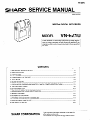
1
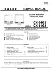
SHARI=
SERVICE MANUAL
S6919VN-EZI U/
MPEG-4 DIGITAL RECORDER
VN-EZI U
1
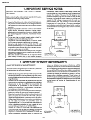
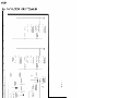
In the interests of user-safety (Required by safety regulations in some countries) the set should be restored to its
original condition and only parts identical to those specified
be used.
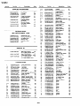
CONTENTS
Page
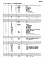
1. IMPORTANT
SERVICE NOTES ......................................................................................................
2. SPECIFICATIONS
l-l
...........................................................................................................................
2-l
3. PART NAMES ..................................................................................................................................
3-l
4. DISASSEMBLY OF THE SET .........................................................................................................
.
5. TEST MODE ....................................................................................................................................
4-l
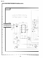
6. BLOCK DIAGRAM ...........................................................................................................................
6-l
7. OSCILLATOR,
7-l
DIVIDING AND MULTIPLY MAP/8. POWER CONTROL FLOW ...........................
9. TROUBLESHOOTHING
..................................................................................................................
5-l
9-I
1O.IC FUNCTION LIST .......................................................................................................................
10-l
11 .SEMICONDUCTOR
1 l-l
LEAD IDENTIFICATION
...............................................................................
12.WIRING DIAGRAM ........................................................................................................................
12-I
13.SCHEMATlC
13-l
DIAGRAMS .............................................................................................................
14.PRINTED WIRING BOARD ASSEMBLIES
15.REPLACEMENT
...................................................................................
PARTS LIST .......................................................................................................
16,PACKING OF THE SET .................................................................................................................
SHARP
CORPORATlON
14-I
15-1
16-I
This document has been published to be used for
after sales service only.
The contents are subject to change without notice.
VN-EZl U
1. IMPORTANT SERVICE NOTES
BEFORE
RETURNING
RECORDER
THE
VIDEO
connections, metal cabinet, screw heads, knobs and
control shafts, etc.) ,and measure the AC voltage drop
across the resistor. Reverse the AC plug (a non
polarized adaptor plug must be used but only for the
purpose of completing these checks) on the set and
repeat the AC voltage measurements for each exposed metallic part. Any reading of 0.45V rms (this
corresponds to 0.3mA rms AC.) or more is excessive
and indicates a potential shock hazard which must be
corrected before returning the video camera recorder
to the user.
CAMERA
Before returning the video camera recorder to the user,
perform the following safety checks.
1. Inspect all lead dress to make certain that leads are
not pinched or that hardware is not lodged between
the chassis and other metal parts in the video camera
recorder.
2. Inspect all protective devices such as non-metallic
control knobs, insulating materials, cabinet backs,
adjustment and compartment covers or shields, isolation resistor/capacitor networks, mechanical insulators etc.
3. To be sure that no shock hazard exists, check for
leakage current in the following manner.
Plug the AC line cord directly into a 120 volt AC outlet
(Do not use an isolation transformer for this test).
. Using two clip leads, connect a 1.5k ohm, IO watt
resistor paralleled by a 0.1 $LF capacitor in series with
all exposed metal cabinet parts and a known ground,
such as a water pipe or conduit.
. Use a VTVM or VOM with 1000 ohm per volt, or higher
sensitivity or measure the AC voltage drop across the
resistor (See Diagram).
. Move the resistor connection to all exposed metal
parts having a return path to the chassis (antenna
(
VTVM
0 AC SCALE 0
>
l
’ -5kims
METAL PARTS
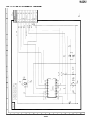
1. NOTES DE SERVICE IMPORTANTES
retour au chassis (connexions d’antenne, coffret
metallique, t&es de vis, boutons et arbres de commande,
etc.) et mesurer lachute de tension CA entre la resistance.
lnverser lafiche CA (une fiche intermediaire non polarisee
doit etre utilisee a seule fin de faire ces verifications.) sur
I’appareil et repeter les mesures de tension CA pour
chaque piece metallique exposee. Toute lecture de
0,45 V rms (ceci correspond a 0,3 mA rms CA) ou plus
est excessive et signale un danger de choc qui doit etre
corrige avant de rendre le magnetoscope a son
utilisateur.
AVANT DE RENDRE LE MAGNETOSCOPE
Avant de rendre le magnetoscope a I’utilisateur, eff ectuer
les verifications de securite suivantes.
1. Verifier toutes les gaines de fil pour etre sur que les fils
ne sont pas pin&s ou que le materiel nest pas coin&
entre le chassis et les autres pieces metalliques dans le
magnetoscope.
2. Verifier tous les dispositifs de protection tels que les
boutons de commande non metalliques, les materiaux
d’isolement, le dos du coffret, les couvercles de
compartiment et ajustement ou les boucliers, les
reseaux de resistance / condensateur d’isolement,
les isolateurs mecaniques, etc.
3. Pour etre stir qu’il n’y a aucun risque de choc electrique,
verifier le courant de fuite de la maniere suivante.
. Brancher le cordon d’alimentation secteurdirectement
dans une prise de courant de 120 volts. (Ne pas
utiliser de transformateur d’isolement pour cet essai).
. Utiliser deux fils a pinces et connecter une resistance
de IO watts I;5 kohm en parallele
avec un
condensateur de 0,15 PF en serie avec des pieces du
coffret metallique exposees et une masse de terre
connue telle qu’un tuyau ou un conduit d’eau.
. Utiliser un VTVM ou VOM avec une sensibilite de
1000 ohms par volt ou plus ou mesurer la chute de
tension CA entre la resistance (voir diagramme).
. Dbposer la connexion de la rbsistance a toutes les
pieces metalliques exposees ayant un parcours de
I
c
VERS PIECES
METALLIQUES
1-I
VTVM
oECHELLECAo
3
VN-EZI U
WARNING :TO REDUCETHE RISK OF FIRE OR ELECTRIC SHOCK, DO NOT EXPOSE
THIS APPLIANCE TO WET LOCATIONS.
/&/AA
CAUTION
This symbol mark means following.
For continued protection against fire hazard, replace only with same type fuse.
(F901; 1.75A 24V, F902; 1.75A 24V,
F903; 1A 24V, F904; IA 24V, F905; IA
24V)
CAUTION: TO REDUCE THE RISK OF ELECTRIC
SHOCK. DO NOT REMOVE COVER. NO
USERSERVICEABLE
PARTS
INSIDE.
REFER SERVICING TO QUALIFIED SERVICE
PERSONNEL.
A
n
1
0
This symbol warns the user of uninsulated
voltage within the unit that can cause dangerous electric shocks.
This symbol alerts the user that there are
important operating and maintenance instructions in the literature accompanying this unit.
ATTENTION: POUR REDUIRE LES RESQUES D’INCENDIE OU DE CHOC ELECTRIQUE,
NE PAS EXPOSER CET APPAREIL A LA PLUIE OU A L’HUMIDITE.
RISQUE DE CHOC ELECTRIQUE
NE PAS OUVRIR
ATTENTION:
A
n
1
0
n
1
ATTENTION
0
AFIN DE REDUIRE LES RISQUES DE
CHOC ELECTRIQUE, NE PAS RETIRER LE
COUVERCLE, AUCUN ORGANE INTERNE
NE PEUT ETRE REPARE PAR
L’UTIUSATEUR, CONFIER L’APPAREIL A
UN DEPANNEUR QUALIFIE.
Ce symbole signale a I’utilisateur la presence
d’une tension non isoleea I’interieurde I’appareil
qui peut etre la cause de secousses electriques
dangereuses.
Ce symbole avertit I’utilisateur que des instructions importantes relatives a I’utilisation
et al’entretien se trouvent dans le manuel
accompagnant I’appareil.
1-2
Ce symbole signifie que I’on devra utiliser un fusible de meme type (F901;
1.75A 24V, F902; 1.75A 24V, F903; IA
24V, F904; 1A 24V, F905; IA 24V) pour
assurer la securite.
A
VNkEZlU
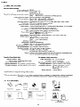
2. SPECIFICATIONS
MPEG-4 Digital Recoder
Power requirement:
Power consumption:
Record format/Image
compression system:
Sound recording system:
Pixel composition:
Recording medium:
Photometry:
Exposure control:
Pickup device:
LCD Monitor:
Lens:
Focus range:
White balance:
Shutter speed:
Self-timer:
Microphone:
Speaker:
Operating temprature:
Storage temprature:
Operation humidity:
Dimentions:
Weight:
DC6V
[Recording] 3.4 W
[Playback] 2.7 W
[Movie] MPEG-4/ASF
JPEG base line conformance/JPEG (Exif 2.1)
[Still]
ADPCM, monaural, 8 kHz sampling
[Movie] 160 x 120 pixels/320 x 240 pixels
[Still]
640 x 480 pixels (square dots)
SmartMedia card (SSFDC) (3.3 V) (2MB, 4MB, 8MB, 16MB, 32MB)
TTL center-weighted average metering
Aperture-priority auto exposure
l/4-inch square pixel color CCD image sensor (with approx. 350,000 pixels
including optical black) progressive scanning
1.8 inch color screen with approx. 61,000 pixels
Fixed focus with macro positon, F=3.4/8 f=3.8 mm
[Normal] t-A approx. 24” (60 cm) to 00
[Macro] aapprox. 4” (10 cm)
Automatic tracking, manual switching (“OUTDOOR”/“INDOOR”)
Auto variable
[Movie] l/l 5 to l/4000 second
[Still]
l/4 to l/4000 second
IO second
Monaural nondirectivity
020 mm 100 mW output (monaural)
O°C to +4O”C (32°F to 104°F)
-20°C to +6O”C (-40°F to 140°F)
30% to 80% (with no dew formation)
37/32”(W)x 317l$‘(H) x 1*‘/32”(D)
[81.4 mm (W) x 89.5 mm (H) x 42 mm (D)]
0.33 Ibs (148 g) [body only]/053 lb (240 g) [including a SmartMedia card,
four AA-size alkaline batteries and a hand strap]
AC Adapter (UADP-0243TAZZ)
Supplied SmartMedia Card
Memory capacity:
Memory type:
Power requirement:
Operating temprature:
Storage temprature:
Power requirement:
DC output:
Operating temperature:
Storage temprature:
Dimensions (approx.):
4MB
NAND flash EEP-ROM
3.3 v
O°C to +4O”C (32°F to 104°F)
-20°C to +6O”C (-4°F to 140°F)
Weight (approx.):
Specifications
AC 11 O-130 V/60 Hz,
DC 6.0 V/700 mA
O°C to +40°C (32°F to 104°F)
-20°C to +6O”C (-4°F to 140°F)
23/8”(W) x 33/8”(H) x 1*‘/32”(D)
[60 mm (W) x 86 mm (H) x
49 mm (D)]
1.08 Ibs (490 g)
are subject to change without notice.
* Minimum ilumination:
Alkaline batteries
(AA-size x 4)
3.3 V type
SmartMedia
(4MB)
Since there is no widely accepted testing procedure for determining minimum illumination
capability, lux ratings are comparable only between models from the same manufacturer.
Hand strap
SmartMedia
Soft case
holder
PixLab Integrated Digital
Media Software CD-ROM
Index label (X 2)
Write-protect
AC adapter
UADP-0243TAZZ
seal (x 4)
Floppy disk adapter for med’iaTM
VR- 1FPN
RUNTK0350TAZZ
VN-EZl U
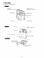
3. PART NAMES
For details on the use of each control.
Lens body --i
(CAME RA/PLAY
Mode select switch
(MOVIE/STILL select switch)
1
POWER
Operation button
MENU button
.
Grip
L_.----
LCD monitor
r
Iris select switch
Hand strap loop
Lens body
(CAMERA/PLAY select switch)
Shutter button
Microphone
Speaker
Focus (Macro/Normal)
select switch
DC IN 6V terminal
Lens
-Tripod
-
3-1
socket
SmartMedia slot
VN-EZl U
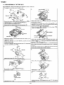
4. DISASSEMBLY OFTHE SET
*For assembly, tighten the screw to the torque of 0.5+0.1/-O kg cm.
*Previouslv remove the smart medium unit.
6.
1.
J
Batter
B
. Remove the screws (
8TAFF)(2pcs.) and ( t@ LXHZ0206TAFN)( 1PCS.).
. Pressing the power PWB to prevent it from floating, lift the main
PWB in the arrow direction. (Take care that the board-to-board
connector is slightly inner than the center.)
. Remove the screw (OLX-HZ0058TAFF)
of the shutter PWB,
and the main PWB will be removed.
Remove the screws ( @ LX-BZ021 OTAFN)( 1PCS.) and (@ LXHZOQ56TAFN)(l PCS.)and (@LX-BZO208TAFN)(3pcs.).
Open the battery lid as instructed with 0.
Remove the front cabinet, lifting it as instructed with 0.
Is unit
7.
ery connector
@Tapping
b
Back lig
connect
PWB FFC
.Remove
JACK PWB
the screws (@ LX-HZ0056TAFN)(l PCS.) and (@I LX. Remove the JAK PWB screw (0 LX-HZ0062TAFF)(l PCS.),the
HZ0062TAFF)(4pcs.).
battery connector, TFT PWB FFC and back light connector, and
. Lift the lens unit, and remove the CCD flex and tilt connector
the
power PWB will be removed.
across the main PWB.
Note: As far as the power PWB is routed to A, connect the black lead
Remove the operation key flex connector and SP microphone
wire of the jack PWB directly to the battery terminal. From A, solder two
connector, and lift the main PWB.
l
lead wires
3.
from the battery terminal to the power PV’!/Band the black lead wire from
the jack PWB to the land near the battery connector.
8.
. Remove the screws (@LX-BZO208TAFN)(7pcs.).
4.
. Remove the screws (@%BZ0208TAFN)(3pcs.).
. Remove the screws (@LX-BZO208TAFN)(2pc.).
. Remove the CCD flex.
. Remove the TFT flex. _p
.
5.
TUT
Pull off TFT in the arrow direction.
IO.
PWB
Q
G
. Remove the CCD PWB.
/ . Remove the screw (6 LX-BZ0208TAFN), and TFT PWB will be
1 removed.
4-I
VN-EZl U
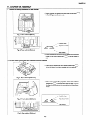
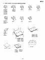
4-1. CAUTION ON ASSEMBLY
I. Caution for wiring treatment of rear cabinet
l
Check whether the flexible and lead lines framed with ()
in the left figure swell out or not.
Fig. 1. Rear cabinet (Whole)
Tripod base holder
Fig. 2. Rear cabinet (Bottom)
l
Check whether the insulation tape is peeled off on the base
holder of the tripod framed with (-)
in the left figure or
not.
2. Cauti
l
Take care to prevent the rear cabinet framed with ()
in the left figure from being outside the front cabinet.
Fig. 3. Rear cabinet (Side face)
l
Take care to insert the projection of the front cabinet
framed with (-)
in the left figure into the area (~
in
the figure below) between the rear cabinet and tripod base
holder.
Tripod base holder
Fig. 5. Rear cabinet (Bottom)
4-2
VN-EZl U
5. TEST MODE
The camera has two kinds of the test mode functions, mode 1 and mode 2, which are used for development/production/service.
5-l. HOW TO ENTER INTO THE MODE 1 (INITIAL SCREEN OF MODE 1)
Mode for setting the CSD display language, clock display and so on
1) Pressing the A key and MENU key, turn on the POWER switch.
f
-
) c-a_:+
I
~
‘.Z.
:::::::::::::
w
.:::
‘I
I+
pg$T
.
..~.Qq$:
J
2) After BUSY is displayed, the initial screen of Mode 1 is displayed.
Initial screen of Mode 1
5-l-l.
Changeover of OSD display language and clock display (linked)
1) Select COUNTRY with A or ‘I key, and select the country display with 4 or ) key.
2) Select NORMAL SET with A or v key, and determine it with ) key.
3) End the setting with POWER OFF.
Country
displav
JP
us
UK
OSD language
displav
1 Japanese
I
Enalish
Enalish
1
Clock display
Year(Y). Month(M). Dav(D)
1
YYYY. MM. DD
1
MM. DD. YYYY
1
DD. MM. YYYY
1
Time
1 AM 12:OO 1
12 o’clock at the daytime is 12:00PM,
1 12:OOAM 1
and 12 o’clock at thenighttime is 12:OOAM.
1 12:OOAM 1
In 24H display, 12 o’clock at the nighttime is
0o:oo.
English
DD. MM. YYYY
0o:oo
EU
* 12H display can be selected for user-set clock
timina.
Note: When the country display is changed, apply “clock timing” in the user setting mode.
5-l-2. Changeover of power save ON/OFF
1) Select P-SAVE with A or v key, and select ON/OFF with 4 or) key.
Setting
Function
P-SAVE ON
Auto power-off is set unless anything is set for approx. 3 minutes.
P-SAVE OFF
Auto power-off is set.
2) Select NORMAL SET with A or v key, and determine it with ) key.
3) End the setting with POWER OFF.
5-l-3. Return of user setting to default setting
Any other user setting except OSD display language setting (Item 5-I -1) is all returned to the default setting.
1) Select DEFAULT SET with A or v key, and determine it with ) key.
2) End the setting with POWER OFF.
5-2. MODE 2 (INSPECTION/ADJUSTMENT
MODE)
[Note]: Since the data of EEPROM is rewritten if any address is selected and the data is changed, not only
carefully operate it but also be sure to record the address and data before setting the data.
Objects, meters and jigs/tools necessary for inspection and adjustment
*Jig/tool name
Part code
AC adapter
Separately available (VR-1 AAW)
Commercially available
Halogen light x 2 PCS.
JiGCHARTGray scale chart
JiGCHART- 1
Siemens Star Chart
JiGMETERllluminance meter (o-3000 lux)
Color temperature meter (1600~400000K)
JiGMETERColor temperature conversion filter (3200+68OOK)
JiGHOYA-LB165
1 HOYA”LB-165”
I
I
Extension cable 30pin, Main (CN204) - Power (CN906)
QCNW-1948TAZZ
Extension cable lOpin, Main (CN202) - Control (CN2901)
QCNW-1949TAZZ
Extension cable 13pin, Main (CN31) - CCD (CNl)
QCNW-1950TAZZ
- - -QCNW_19~TAZ~
Extensioncable
%in~P~~(~%7~
wT(CN803)
5-I
Price code
BB
Remarks
CP
CE
CT
FF
BH
I
BS
AP
AP
-
-AK
New
New
New
-
-
-
New
-
How to enter into the test mode (initial screen of TEST MODE)
1) Pressing the V key and MENU key, turn on the POWER switch.
2) When BUSY is displayed on the screen, release the V key and MENU key, and
the initial screen of the test mode will be displayed. (Refer to the center of the
following figure.)
3) Shift to each mode with the operation button of the main unit.
4) After setting is completed, press the MENU key, and it will return to the initial
screen of the test mode. Then turn off the power.
/
n
0
a
0v
‘I>
+
POWERm
..:‘.
Color bar pattern
W/Y/Cy/GIMglRIBluelBlack
t
Initial screen of TEST MODE
Screen of EEPROM SET
Initial screen of EEPROM INI
Screen of WB ADJ
Version display +
5-2-l. Method of displaying the test pattern
To inspect and adjust the liquid crystal the color bar and monochrome pattern can be displayed.
mMethod of displaying the color bar (75% modulated)
1) The initial screen of the test mode is displayed.
2) Press the A key to display the color bar.
3) Press the MENU key, and it will return to the initial screen of the test mode. Then turn off the power.
mMethod of displaying various patterns
1) The initial screen of the test mode is displayed.
2) Press the 4 key to display EEPROM SET screen.
3) Press the 4 key to display Address 1FE of EEPROM.
4) Press the A key to set 00 as the data of Address 1FE.
5) Press the A or V key to vary the data, and the patterns in the following table will be displayed.
Data (h)
01
Address (h)
IFE
Display pattern
I
White signal 40%
1 White s&al 100%
1 Black signal
1 Color bar signal
I
02
03
1
04
05
Red signal:The signal level is the same as that of the color bar.
I
06
07
1 Green signaLThe signal level is the same as that of the color bar.
I Blue signal:The signal level is the same as that of the color bar.
i
I
I
J
6) Set FF as the data of Address IFE of EEPROM.
7) Press the MENU key, and it will return to the initial screen of the test mode. Then turn off the power.
5-2
I
I
5-2-2. Method of selecting VALID/INVALID
of the battery lid switch
For disassembly and operation, set the switch of the battery lid at VALID.
1) The initial screen of the test mode is displayed.
2) Press the 4 key to display EEPROM SET screen.
3) Select Address 1 FD with 4 or ) key, and set FF as the data with A or v key.
4) Press the MENU key, and it will return to the initial screen of TEST MODE. Then turn off the power to complete the setting.
Since the battery lid switch becomes invalid, it can be disassembled for inspection and repair.
[Note]: After the inspection and repair are completed, be sure to return the data of Address 1 FD to 00 (except FF), and turn the battery
lid switch to VALID.
5-2-3. Method of adjusting the LCD display
For adjustment, remove TFT PWB from LCD unit.
a) Horizontal position adjustment
1) The initial screen of the test mode is displayed.
Select Address 1 FE with 4orb
key, and set the data at 04 with
the wh ite and black bars at both ends of the color bar displayed
+To POWER PWB
I
L-l-,
I
v
JTo POWER PWB
4) After adjustment, set FF as the data of Address 1 FE with A or v key.
5) Press the MENU key, and it will return to the initial screen of TEST MODE. Then turn off the power to complete the setting.
b) Common bias adjustment
[Note]: Apply this after aging of approx. 5 minutes. The back light set by the user is regarded as standard.
1) The initial screen of the test mode is displayed.
2) Press the 4 key to display EEPROM SET screen.
3) Select Address 1 FE with 4 or ) key, and set 00 as the data with A or v key.
4) Bring the lens unit into the shooting state (EE display).
5) Select Address 1 F8 with 4 or ) key.
6) Shoot the gray scale, and vary the data with A or v key to find such a point as the black sinks to the deepest.
7) After adjustment, select Address 1 FE with 4 or ) key, and set FF as the data with A or v key.
8) Press the MENU key, and it will return to the initial screen of TEST MODE. Then turn off the power to complete the setting.
c) White balance adjustment
[Note]: Apply this after aging of approx. 5 minutes. The back light set by the user is regarded as standard.
1) The initial screen of the test mode is displayed.
2) Press the 4 key to display EEPROM SET screen.
3) Select Address 1 FE with 4 or ) key, and set 01 as the data with A or v key.
(White 40% pattern is displayed.)
4) Bring the sensor unit of the color thermosensor into contact with the screen of
the LCD monitor, and measure the color temperature (M) and.compensation
value (CC).
[Note]: To prevent the LCD monitor screen from being injured at this time,
don’t press the sensor unit of the color thermometer or rub it.
To gain the color temperature of 7600 +_200K and the compensation value of 50 +_2, select Address 1 F5 or 1F6 with 4 or ) key, and
adjust the data with A or v key.
[Note]: Take the measurement 2 or 3 times to reduce the error.
Select the dark place to prevent an excess light from entering the sensor unit of the color thermometer.
First adjust the color temperature into the standard range, and adjust the compensation value (CC).
5-3
VN-EZl U
Color temperature
Low
High
Low
High
Low
High
Within standard
Within standard
Within standard
Compensation
value
Low
Low
High
High
Within standard
Within standard
Low
High
Within standard
Address 1 F5 (B) 4
‘IDown
Fixed
Fixed
AUP
VDown
Address 1 F6 (R) )
Fixed
VDown
I
AUP
Fixed
I
AUP
AUP
VDown
VDown
AUP
Adjustment end
AUP
Adjustment end
VDown
5-2-4. EEPROM INI (initial) method
Apply this when EEPROM is replaced or the version of the microcomputer is increased.
nAdjustment preparation and check items
Before entering the initial screen of the test mode, insert the smart medium in which data is already written.
Moreover, check the version.
Initial screen of TEST MODE
Version display +
Screen of EEPROM INI (PRO)
Screen of EEPROM INI
Screen of EEPROM INI (ALL)
a) PRO (protect) mode
Rewrite the other data except the white balance setting, TFT setting and clock with the data in the smart medium-l) The initial screen
of the test mode is displayed.
1) The initial screen of the test mode is displayed.
2) Press the ) key to display EEPROM INI screen.
3) Press the 4 key to display INI (PRO) screen.
4) Press the shutter button to rewrite the data with the data in the smart medium.
In approx. 1 second, it will automatically return to EEPROM INI screen.
5) Press the MENU key, and it will return to the initial screen of TEST MODE. Then turn off the power to complete the setting.
6) Perform steps in “5-l-2. Return of user setting to default setting”.
7) Then turn off the power to complete the setting.
b) ALL mode
Rewrite all data of EEPROM with the data in the smart medium.
1) The initial screen of the test mode is displayed.
2) Press the ) key to display EEPROM INI screen.
3) Press the ) key to display INI (ALL) screen.
4) Press the shutter button to rewrite the data with the data in the smart medium.
In approx. 1 second, it will automatically return to EEPROM INI screen.
5) Perform steps in “5-2-3. Method of adjusting the LCD display” and “5-2-5. Camera (CCD white balance) adjusting method”.
6) Press the MENU key, and it will return to the initial screen of TEST MODE. Then turn off the power to complete the setting.
7) Perform steps in “5-l-2. Return of user setting to default setting”.
8) Then turn off the power to complete the setting.
*Use the smart medium, FD adaptor or PC card which is copacked or optional.
5-4
5-2-5. Camera (CCD white balance) adjusting method
Preparation and check items before adjustment
For illumination, apply the approximation of the color temperature
lamps are preferable for the even illumination.
Use the chart which is not stained or discolored.
3200K and illuminance 3000 lux, and the light source of 2 or more
Initial screen of TEST MODE
1
I
,
I
During adjustment
Screen of WB ADJ
MENU
Adjustment end
(CMP-ADJ)
I
1
I
i
I
i
I
i
Press the ) key for changeover.
(AUTO) position is used for
investigation but not used for
the service.
1) The initial screen of the test mode is displayed.
2) Press the V key to display WB ADJ (3200) screen.
3) Shoot the gray scale chart.
4) Press the shutter button, and wait until CMP-ADJ is displayed.
5) Press the ) key to display WB ADJ (6800) screen.
6) Set up the color temperature replacement filter (LB-165 3200K -+ 6800K conversion) in front of the lens.
7) Press the shutter button, and wait until CMP-ADJ is displayed.
8) Press the MENU key, and it will return to the initial screen of TEST MODE. Then turn off the power to complete the setting.
5-2-6. Lens back focus adjusting method
Preparation before adjustment
Remove the front cabinet of the main unit, and remove the cabinet of the lens section.
(The cabinet of the lens section can be disassembled or assembled only when the front
cabinet of the main unit is removed.)
Remove the macro adjusting ring. (Refer to the right figure.)
Remove two tilt holder fastening screws on the main unit side, and holding the tilt
section and CCD PWB section with left hand, pinch both ends of the macro adjusting
ring with right hand, and gradually pull it up in the arrow direction. (At this time, take
care to prevent missing the macro ring fastening hardware.)
During adjustment, keep the front cabinet of the tilt holder main unit and the rear
cabinet of the camera in the assembled state, and the main unit will be stabilized.
[Note]: Take care to prevent applying a forcible force to the tilt section.
5-5
I
Tilt holder fastening screw position
I_L
Distance of objet t : 1000&l
Barrel section
Adjusting method
1) When shooting, align the center of Siemens star chart to that of the motor screen.
2) Turning the barrel section of the lens with finger, adjust the lens focus to be the best, checking the monitor screen.
3) Align the macro adjusting ring to the position (level the notch rightward) in the figure below, and straightly insert the barrel from
the front side without moving the barrel.
Hole Dosition of macro adjusting ring and CCD PWB
y
Macro adjusting ring
Macro ring fixture
4) Insert the macro ring fixture into the macro adjusting ring.
Check after adjustment:
Verify that the object is focused in the range of 45 cm to near the infinite point.
5) Assemble the cabinet. Align the macro switch knob of the cabinet to normal, and make an assembly by inserting the inside switch
lever to the notch of the macro adjusting ring.
[Note]:
@Before assembly, verify that the lens and cabinet inside are not stained.
l When assembling the front cabinet of the lens section, the focus switching knob must be positioned at the ordinary shooting position.
l When assembling the front cabinet of the main unit, take care to prevent pinching FPC which is present between CCD PWB and
main PWB.
5-6
VN-EZl,U
Objects, instruments and jig/tools necessary to serve
l
Illumination meter
l
Gray scale chart
l
Color temperature meter
l
Color bar chart
l
Color temperature conversion filter
l
Halogen lamp: 2 PCS.
HOYA “LB-1 65”
JACK PWB
CCD PWB
CONTROL PWB
Color video monitor
Extension cables
l
l
SHUTTER PWB
POWER PWB
8
lrl
L
IO
TILT PWB
Smart Media Socket
To video
monitor
I1
jIl.
TFT PWB
fY
TFT Unit
SP Mic
Service of camera section
NO.
1
Name
I
Part No.
1
Code
1
Gray Scale Chart (390 x 520 mm)
JiGCHARA-1
CP
2
Color bar chart (240 x 320 mm)
JiGCHART-
DA
3
Illumination meter (0 to 3000 lux)
JiGMETER-
Color temperature
1 Note
1
I
JiGMETER-
(1600 to 400000 degrees K)
5
1 Configuration
JiGHOYA-LB165
conversion filter
BH
(3200 degrees K a 6800 degrees K)
JiGCHART-
1
CE
JiGTD1500RTDH
CB
6
Siemens star chart
7
Torque driver (1.5kg.cm)
8
MAIN PWB (CN204) -
POWER PWB (CN906) 30pin
QCNW-1948TAZZ
BS
9
MAIN PWB (CN202) -
CONTROL PWB (CN2901) IOpin
QCNW-1949TAZZ
AP
IO
1 POWER PWB (CN907) -
Note:
1. The color temperature
IQCNW-1950TAZZ
TFT PWB (CN803) 13pin
1
AP
conversion filter (jig name No. 5) is available from Hoya Kogaku in your district.
5-7
1.1.
I,
:::
:::
:.:
::.
:.:
:::
.:_
IL
is
.:.:
I:!:
b
$
....
.i.
.I._
::::
~._rnl,
::::
w
..
::::
::::
;:;:
.:.:
::::
::::
::::
>;.
ii;
....
ig
$5
:i::
;_
/wa
IJL
VlO%LO
zoz-31
wvtiaw91
ZZVl869OXI
soz-31
~a~ndumom!w
i
i
I
i
i
i
1’11
..I.
.
.-1;
>
t:
\
,...........................A
‘0:
I
L
k
Ja&laAu(
1
Oap!/\
II I
Ii/l
ma03
tl
Gu!pnpu!)
twwooz
6uqsaaoJd
ieu6!s
a33
5.
)
. ... . .. . ... .. . ... . . 8
..
v
~pgs/a!~oyy fjiiiii;i&.jg’
ZZbOOLOXI-Htl 101-31
31s~ 6u!ssaaoJd p~6~s
a6txu!
6u!pni~u!)
yxqhld
J8pOXl~
Ma
.* :. . . . . . . . . . . . . . . . . . . . . . . . . . . . .
I
f
. I(luo 6u!~ooys a!/\oyy 2:; tju!~ooys a!AOw
Y
I
Jaj_4aAuoz
3ana
I
I
rl
I
.
.
.
.
.
.
.
-a
I
j.~eya MO14 IT&!S
J
80L6W
LO6-31
JaMOd
. . . . . . . . . . . . . . . . ..
l
.;
~lgs/a!~op,j (?%~i6ii~~mi
l-/9lLLWSWIHA
z09-3l=Po~ =!oA
6u!9ooys a6eu4
.
.
.
.
.
.
,
:
.
.m
31w
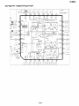
VN-EZl U
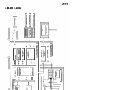
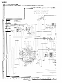
7. OSCILLATOR, DIVIDING AND MULTIPLY MAP
X801
CCDICDSIAD
12.2727
MHz
ASIC
443s -f
[ 0sE-j
I
I
I
I
l/2
l/7
x3
l/70
l/3068
D&K
P&K
CL
P_SCNC
D&K
I
+
4
4
+
Microcomputel
SD-RAM
DSP ‘t
I
73.6362
MHz
3.506486
MHz
TFT control
IR3R29M
I
DC-DC
I
73.6362
I
350kHz
8. POWER CONTROL FLOW
ON
I0.8s
10.6s
1
power SW
I
Unless pressed 0.5 see or more,
it will not be turned on. (Prevention of wrong operation)
PCNTl
I
DC-DC converter ON (Microcomputer ON)
Terminal name
PCONTI
PCONT2
BLCNT(normal)
+5V (CCD)
+I 5V (CCD)
PCNT2
Circuit ON
BLCNT
I
I
Back light is lit.
-9V (CCD)
+B (Audio)
+3.3V (MEDIA)
+3.3V (RTC)
+3.3V(LSI)
+2.5V (LSI)
When battery lid is opened,it will be turned off here.
+2.5V (LSI)
-15V (TFT)
+7.5V (TFT)
+I 5V (TFT)
+5V (TFT)
7-1
Battery(V)
3.3
3.3
3.3
Measurement terminal
CN906-10
TL949
TL952
CN906-13
CN906-30
TL973
5
CN906-1
TL917
15
-9
6
CN906-2
CN906-3
CN906-4
CN906-5
TL921
TL925
3.3
3.3
3.3
2.5
2.5
-15
7.5
15
5
CN906-6
CN906-7
CN906-8
CN906-9
CN907-7
CN907-8
CN907-9
CN907-IO
TL929
TL933
TL937
TL941
TL944
TL945
TL975
TL979
TL983
TL987
IC205 TROUBLESHOOTHING
9. TROUBLESHOOTHING
No
Is the terminal (21), (28), (32) (33) (47)
(48) (50) (82)s GND, (9), (29) (34) (35)
(40) (49) (77) or (79) of microcomputer
power [3.3V] is normal.
POWER CIRCUIT TROUBLESHOOTHING
Check power circuit.
Check L208.
-,
The power cannot be turned on.
RSTX(75)“H”
Isvoltage
output between the pins (2),
(3) (6) and (7) of Q921 and TL1922?
No
Check battery terminal.
Check F901 and F902.
No
B Check periphery of Q924. Check SW291 1.
Is PCNTl at Hi level?
Check microcomputer
circuit.
No
l Check C906, R902 and R905.
Is 2.5V output to TL944?
keys (36)
(37) and (38)
*
Check C903 and R910.
Is IC2901 communication
I
‘No
l
No
b
Check F903, F904 and F905.
Check L904 and D906.
No
Check relevant key.
Check R2901 -R2908 and R291 O-R291 2.
l
1
Shorted load of 3.3V line.
normal?
lines of lC205 and lC2901.
(32
kHz).
.
r
No
b Check pins (l), (2), (99)
and periphery of IC201.
(loo),
(83)-(90)
I Yes
No
and (9) of IC901.
Shorted
Check connection
lI Check
IC2901 for oscillation
-
I Yes
l Check Q906, D905, L905 and pins (8)
No
No
normal?
I
Is IC201 communication
+
Check pins (91)-(98),
periphery of IC203.
(83)-(90)
and
load of 2.5V line.
l Check Q928 and IC903.
Yes
a
L
b Check IC201 oscillation.
(24.5454MHz)
Check connection lines of IC205 and lC206.
Yes
v
No
I Yes
Yes
Is 3.3V output to TL943?
to pin
I Yes
Yes
Is voltage supplied to the emitter of
Q930, Q906 and Q907?
4 MHz) supplied
l
&eoi;ration
Yes
Is triangular wave of approx. 700 mVp-p
output at the pin (17) of IC901?
Is clock (approx.
(80)?
l Check battery and AC adaptor.
Yes
Is OV applied to the pin (13) of IC901
when power is turned on?
Check IC204 and D201.
I
Check SW901.
Defective
IC205.
Short circuit of each pin.
Yes
l
Shorted load of 5V (CCD) and 5V (TFT) line.
Check IC904, Q930, Q911, IC906, Q908, D906,
L911, L904 and pins (11) and (12) of IC901.
Is 5.OV output to TL919 and TL989?
Yes
Shorted
load of 3.3V (MEDIA)
1 IC205 normal.
CCD TROUBLESHOOTHING
line.
1Turn mode SW to MOVIE.
Is
Is
Is
Is
15V applied
7.5V applied
-9V applied
-15V applied
to TL923 and TL983?
to TL981?
to TL927?
to TL977?
No
l Shorted load of 15V (CCD), -9V (CCD), lSV(TFT),
.
Is back light lit?
Does T903 oscillate?
I
+
.
I
I Yes
+
1
No
No
1 Is power voltage no-1
7.5V (TFT) and 15V (TFT) line
Check Q907, T901, 0907,0908,
L907, L908, L909,
L910 and pins (15) and (16) of IC901.
Is clock signal supplied
and TL17?
I
Check Q922, Q923, Q925,
Q929, L913 and C946.
to TL15, TL16
of the
l Check IC35 and periphery of IC201.
Check CCDFPC.
No
b Check IC31 and its periphery.
Check CCDFPC.
I
Yes
Is pulse signal supplied
or LCD unit is defective.
Refer to the troubleshooting
1 power supply.
No
I Yes
b48
d
to TLG-TLlO?
1
Yes
Is signal supplied
to (l)-(4)
and (12)-
Check ICl peripheral
(141 of Cl?
ICl is defective.
Check Ql.
CCD unit is normal.
circuit.
I
I
CAMERA TROUBLESHOOTHING
AUDIO TROUBLESHOOTHING
LCD TROUBLESHOOTHING
1Turn mode SW to MOVIE.
Turn mode SW to MOVIE.
(Shooting mode)
Abnormal
Picture is not displayed.
LNo
Is LCD monitor normal?
Is OSD output?
-b
No
Is the terminal (12) (17), (33), (39),
(40) (42), (43) or (44) of power [3.3V]
of IC34 normal?
No
_
Refer to the troubleshooting
LCD supply.
of the
l Refer to the troubleshooting
CCD supply.
of the
r
b
I
b Refer to the troubleshooting
power supply.
Check IC33, L31 and R44.
of the
Check R650 and R651.
Is the voltage of approx. 2 V output to
Is -15V supplied to TL849, 7.5V to
TL853,15V to TL857 and 5V to TL860?
TL604?
I Yes
v
Is signal output at pin (25) of IC602
when normal microphone is connected
and signal is supplied?
+
Check pins (24) and (25) of IC602,
l and Q652, Q653, FB603, FB604 and
their periphery.
I Yes
Check IC201 and their periphery circuit.
Is signal supplied to (18) and (20) of
IC602.?
No
Are pins (1 l), (13) and (14) of IC602
properly connected to IC205?
Yes
-No supplied to
Is approx. 1 .OV voltage
+
I Yes
+-No
Are 6 to 9V common signals output at
TL824 and TL868?
b Check IC802 and their periphery.
No
b Check IC205 and their periphery.
I
No
+ Check IC806, its periphery, and IC806
to IC205 connection.
No
d Check lC801 and X801.
Check IC801.
Is signal output at TL831, TL832 and
TL833?
IC34 is defective.
Check IC201 and their periphery.
1
No
,
1Yes
I
b Check the pins (4) (5) and (6) of fC602
as well as R604 and R605.
Medium is not read.
1
I Yes
Check C603 and R603.
Defective medium
Is the signal output to TL601 and
TL602?
i
No
’
Check IC601, its periphery, FB601 and
FB602.
1Yes
Formatting with PC
Yes
I Yes
No
1Check the speaker.
+ Check the smart medium socket, lC201
and its periphery.
No
Medium normal.
1
Yes
1 Defective LCD unit or FPC wire breakaae
1 IC201 is defective.
Check IC201, its periphery and Q201.
Check TFT FPC.
Yes
IC602 is defective.
Yes
of the
No
1 IS IC801 oscillated at
Is signal output at pins (4) and (6) of
IC602?
Refer to the troubleshooting
b power supply.
Check TFT FPC.
IS video signal suppm1
Is approx. 2.4V signal output at pin (2)
of IC806?
b Check connection line of IC205.
Is output signal output to A/D output
(2)-( 11 )?
of the
I Yes
Check IC201 peripheral circuit.
I
No
I Yes
No
Refer to the troubleshooting
power supply.
Is back light lit?
Check CCDFPC.
Is clock signal supplied to (16), (21)
and (22) and pulse signal supplied to
(20) and (23)?
7
I
VN-EZI U
10. IC FUNCTION LIST (IC205:IXO698TA)
Micom Pin No.
1
2
3
4
5
6
7
8
9
IO
11
12
13
14
15
16
17
18
19
20
21
22
23
24
25
26
27
28
29
30
31
32
33
34
35
36
37
38
39
40
41
42
43
44
45
46
47
48
49
50
51
52
53
54
55
56
57
58
Micom Port Name
P22
P23
P24
P25
P26
P27
P30
P31
vss
P32
P33
P34
P35
P36
P37
SIN0
SOT0
P42lSCKO
P43
P44
vcc
P45
P46
P47
P70/SDA
P71/SDA
P72
DVRH
DVSS
DA0
DA1
AVCC
AVRH
AVRL
AVSS
AN0
AN1
AN2
AN3
vss
AN4
AN5
AN6
P57/AN7
IRQO
P81/IRQl
MD0
MD1
MD2
TEST
P82/l RQ2
P83/l RQ3
P84
P85
P86/0UT3
NC
P60
P61
I/O
0
0
0
0
0
0
I
Signal Name
PRO
PBUSY
DSPRESET
CCDCNT
PCNTI
PCNT2
BLCNT
PWMODE
I
I
I/O
0
0
I
I
0
LENSSW
TFTINVSW
RTCDA
RTCCL
PO
SHTR
SIN
SOT
Lens direction detection (Low: Playback)
TFT inversion detection (Low: Reverse)
RTC data input/output
RTC clock
Camera circuit power control (Low: Playback)
Shtter input (Low)
RS232C data input
RS232C data output
I/O
0
EDAT/ESDA
TFTINVO
EEPROM
TFT inversion setting output (Low: Reverse)
0
I
0
ESHIFT/ESCL
ACDTCT
0
0
AGCI
AGC2
I
I
I
I
KEY1
KEY2
MODE
BATT
I
I
PWERR
TEMP
I
PINT
VCAM
I
I
I
I
0
MD0
MD1
MD2
H:Single chip operation mode specification
H:Single chip operation mode specification
L:Single chip operation mode specification
H fixed
0
0
BLCH
TFT brightness switch (Low: Dark)
0
0
DEN
COIN
Open terminal
AUDIO codex (DataEnable)
AUDIO codex (ContolDataln)
I
RST
ACT
L
L
L
L
H
H
H
H
H
L
L
Function/Connection
VCAM
VCAM
DSP reset output
CC0 power circuit
Power circuit
Power circuit
TFT back light power
Power SW detection (Low)
block
EEPROM
AC adaptor detection
Open drain output
Open drain output
Open drain output
Open drain output
DA converter external reference power terminal
DA converter power terminal
Camera circuit
Camera circuit
AD converter power terminal
AD converter external reference power terminal
AD converter external reference power terminal
AD converter power terminal
Operation unit
Operation unit
Operation unit (Static picture/dynamic picture)
Power voltage detection
Power short circuit detection
Temperature detection
IO-I
VN-EZl’U
r
Micom Port Name
Micom Pin No.
59
*
P62
60
PPGOO
P64
61
62
P65
63
P66
64
P67
65
P90
66
P91
67
P92
68
P93
69
P94
P95/ZlNl
70
71
P96/lNO
72
P97/lNl
I
73
PA0
74
PA1
75
RSTX
76
PA2
77
XOA
XIA
78
vss
79
x0
80
Xl
81
82
vcc
PO0
83
84
PO1
85
PO2
86
PO3
87
PO4
88
PO5
PO6
89
90
PO7
PI0
91
PI1
92
PI2
93
PI3
94
PI4
95
96
PI5
PI6
97
98
PI7
99
P20
100
P21
I/O
0
0
0
0
0
Signal Name
DCLK
BEEP
PDN
DSPPO
DSPPI
I
I
0
I
I
0
0
CD
LVD
PRTCTO
MEDIA
PRTCTI
XRST
TFTXRST
I
I
lol
lOI
I I I
IW
FIST
ACT
L
Function/Connection
AUDIO codex (DataShift)
AUDIO codex (PWI)
AUDIO codex (PowerDown)
DSP boot selection
DSP boot selection
SSFDC
SSFDC
SSFDC
Lid open detection (High : OPEN)
SSFDC soket (Low : protect)
Reset output (VCAM)
TFT reset output
H
DADI
DACK
I
t
1
I
1
I
DALD
l
I
block
I
1 DA converter data
1 DA converter clock
l
l
Reset input terminal
DA converter road
I
I
I
I
I
I
I
I
I
DBO
I/O
DBI
I/O
DB2
I/O
DB3
I/O
DB4
I/O
DB5
I/O
DB6
I/O
DB7
I/O
DSPHCS
0
DSPHAO
0
DSPHAI
0
DSPHRD
0
DSPHRE
I
1 0 1 DSPHWR
1 I 1 DSPHWE
0
DSPHINT4
0
PADREN
0
PWR
(24.5454 + 7MHz) Clock input terminal
1
1
1
1
1 o-2
DSPNCAM
DSPNCAM
DSPNCAM
DSPNCAM
DSPNCAM
DSPNCAM
DSPNCAM
DSPNCAM
DSP
DSP
DSP
DSP
DSP
1 DSP
1 DSP
DSP
VCAM
VCAM
data
data
data
data
data
data
data
data
bus
bus
bus
bus
bus
bus
bus
bus
I
I
VN-EZl U
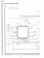
11 SEMICONDUCTOR LEAD IDENTIFICATION
n
&@$
@
B
4
2SC-2404-C
2SC4081 R
DTCI 44EE
2SA1362GR
DTCI 14YE
DTCI 1SEUA
2SC4213B
XC62EP25
XC62EP50
TC7SH04U
RB451 F
3
4
+
4(C)
DA227
2SA1314C
2SB1121T
2SD874A-RI E
2SK2316
%
+
%
G2
DA221
51
25
A
.
C
1SS368
HVlJ359TR
Fl AJ3
Fl J2F
Sl6463DQ
2
Q
A
+
1
S80827LN
50
30
20
5o
25
15
10
1
25
37
76
IX0750TA
MB8346B
MSM7716
MPDI 650
48
100
’
IR3Y29AM
BA9708KV
VSP2000
IX0701 TA
IX0698TA
(48Pin)
(32Pin)
(48Pin)
(1 OOPin)
(1 OOpin)
5
7
1
LEOP3641
IX0700TA
(176pin)
1
S3530A
NJM4565V
TC7W14U
Sl6463DQ
NJM2113V
TC7WH04U
S24C04A
11-l
(5OPin)
(20Pin)
(30Pin)
(20Pin)
VN-EZl U
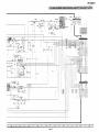
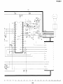
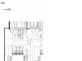
12. WIRING DIAGRAM
Over
Allf
DUNTK290lQAOs
QPWBX2901TAwk
CN3 I
N I 393TA
CAMERA
DUNTK2905PMOO
QPWBX2905TA**
;; /‘,5V(cCD)
, , v2
1
I
CCD
I
/
I:;5V(CCD)
r---_--__----------_--_-_---------~~---~
I;/
j
I
I
I
I
I
I
I
I
I
I
I
I
I
I
I
I
I
I
I
(CAMERA)
-------e-t
---------I
I
I
I
I
I
I
I
I
I
I
I
I
I
(AUDIO>
(RMICC0087TAZZ
CN60 I
N0276T.
SF
SPEAKE
t-
SPEAKE
------s-J
--------,
I
I
I
I
I
I
I
I
El
26
25
I
I
I
I
I
I
I
I
I
I
I
I
I
I
I
I
I
I
I
I
I
1
I
I
I
I
I
MEDIA
SOCKET
PIN
CN204
W3062T.
POWER
.NO
I
“ONTROL
L
PWB 1
1
(RECl
%%%TA
REC
?
NC
3
PCNTZ
$
BATT
J
PSYNC
j
ACDTCT
7
DADI
3
TFTXRST
3
VICE0
3
TFTIN
I
DACK
2
DALD
3
AlUGtQ
4
GN)
5
GN>
5
P-SW
7
POW
3
BLCH
3
PbERR
t
BLCNT
,
I
I
I
I
I
I
I
I
I
DUNTK2902PMOO
QPWBX2902TA**
3
‘,
CN203
N0363TA
TILT
I
I
I
I
I
I
I
I
I
I
I
I
I
I
CN207
N0474TA
12-I
PWE
SHUT
VN-EZl U
SPEAKER
(VSP0020P-968N)
TFT
PWB 1
DUNTK2904QAOO
QPWBX2904TA**
TFT
UNIT
RLCDV0050TAZZ
CN60
I
N0276TA
I
I
I
I
I
I
I
I
--A
--3
I
I
I
I
I
I
I
I
I
I
I
I
I
I
I
I
I
I
I
I
I
I
I
I
I
I
I
I
I
I
I
CN204
W3002TA
DUNTK2900QAOO
QPWBX2900TAwk
-
I
I
I
I
I
I
I
I
I
I
I
I
I
I
I
I
I
I
I
I
I
I
I
I
I
I
I
I
I
I
I
I
1
I
I
I
I
I
I
I
I
I
I
---I
CN203
N0363TA
TILT
PM3
,
,
(
VN-EZl U
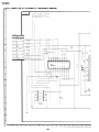
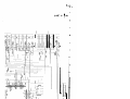
13. SCHEMATIC DIAGRAMS
13-l. POWER SCHEMATIC DIAGRAM
* See Page 13-16 When replacing expansion fig of IC901.
DUNTK29OOQAOO
QPWBX2900TA**
REC
PLAY
r
5.0
1
r5.0)
0
D918
rol
I SS368
IJAPAN
II 2023TAZZ
IL2524TAZZ
2,
2
6.0
(6.01
IOTHER
IL172lTAZZ
IL I72 I TAZZ
r
R925
I50
R905
IK
R902
330
1
I
2
I
3
I
4
I
5
I
13-1
6
I
7
I
8
I
9
I
IO
I
VN-EZlU
1
TO
BACK
LIGHT
Q929
A I 362GR
R995
I6J
RI925
3.9
0049TA
FE910
3
I
OTL917
OTL919
0TL921
0TL923
FB912
_
0TL925
oTL927
FB913
_
OTL929
FB906
_
0 TL933
FB907
_
0 TL937
0 TL940
0 TL939
FB906
_
OTL94I
OTL942
OTL943
FB91
_
I
FB909
_
OTL930
-
OTL931
0TL935
0 TL946
0 TL944
~
oTL945
0TL947
1
+SV(CCD)
2
+I5V(CCD)
+
3 I
-9V(CCD)
1-1
4
+B(AUDIO)
-+
5
+3.3V(MEDIA)
+
6
+3.3V(RTC)
+
7
+3.3v(LsI)
+
8
+2.5V(LSI)
+
9
+2.5V(LSI)
-+
PCNTI
t
MEDIA
t
AlO
OTLg5’
I I
I
TL’g34
I
FB902
FB903
I
ACDTCT
o
17
DADI
t
OTLg6’
18
TFTXRST
C
TL975
0
TL977
0
7
TL979
0
TL961
0
8
TL963
0
TL965
0
g
TLg67
o
TLg8g
o
10
TFTXRST
I
I
* TLg55 I 61
6
FB90
+
1-t
+
-ISVtTFT)
+
+7.5V(TFT)
-+
+I5V(TFT)
+
+SV(TFT)
+
FB904
0049TA
R94 I
W?
4.7KD
R942
v&-z
62K
D
R943
v
1 .2KD
R947
IOOD
c955
560P
5ov
i+
I
IO
I
11
I
12
I
13
I
14
I
13-2
15
I
16
I
17
I
18
I
19
VN-EZl U
13=2-(l). MAIN CIRCUIT SCHEMATIC DIAGRAM (CAMERA)
CAMERA
[
J
QPWBX29OITA+i%
I
I
CCD
-
-i
T
3
L
1
I
-
I
I
I
I
I
I
I
I
I
I
I
I
I
I
R45
I
0
I
-L
c3a
O.lu
IOV
F
-_(AGC
I1.
es
0
(0)
-_(AGC2).
c39
I?
O.lu
IOV
t-g-@
3.4
E
(3.41
c40
O.lu
IOV
L
I
C
IOV
R39
IK
I
I
R40
IK
R4l
IK
es
0
I
fOI,
R42
IK
I
\
C
/.7
I
O
(01
,
3
J
f/.71
c55
O.lu
IOV
4
IC35
TC7WH04U
B
PL
1
I
2
I
3
I
4
I
5
I
13-3
6
I
7
I
8
I
9
I
10
a
(
)
~~(DATcK
>
CCD
CCD
C38
0.1
IOV
R
AVSS2
AGC I
AGC2
AVSS3
c39
0.1
IOV
AVDD I
INT
BIAS2
AVSS
INT
1
CCDD9
D
BIASI
-
CCDD8
1
CCDD7
>
CCDDG
1
CCDD5
>
CCDD4
>
CCDD3
1
CCDD2
1
CCDD I
>
CCDDO
1
AGC I
)
AGC2
)
VIX
)
v2x
)
_
c43
IOU
IOV
10
I
11
I
12
I
13
I
14
I
13-4
15
I
16
I
17
I
18
I
19
VN-EZI U
1a-2-(2). MAIN CIRCUIT SCHEMATIC DIAGRAM (AUDIO)
AUDIOI
R605
I 5K
0
R60 I
I5K
CN60 I
N0276TA
R604
o-
-
II
IOK
__I
ILbUl
SPEAKER
+--
SPEAKER-
’
e-
SPEAKER+
2
603
FB60 I
008lTA
5
F:
88? ! d\l/”
I
o-
R602
n
IC60
0
(01
7
NJM2
I
I lI 3V
C60 I
’ IOU
’ IOV
A
8
,_
F
2.6
(2.6,
I
R62
27K
I
A1362GR
: R623
470
0603
Cl 14YE
IC605
VN-EZI U
R65 I
I 00
R650
6 .8K
C650
33u
I ov
Q652
o C42 13B o
1
1 R’658
I 5K
5
C2
4uxo
C3
40UT+
PBO
AOUT-
NC
=w1
NC
VFO
MAO
-s-@
+%
I
+%-@
I
PBIN
3.4
(3.41
Q653
C408
\
C654
O.lu
0 co/’
‘8
I
CN602
N0263TA
I
MIC
TL604
\
c
t
I I
Olu
l6V
15
7
\JC
UC
NC
C9
NC MSM77’16
NC
VDD
PDN
DCLK
SYNC
NC
CDIN
BCLK
PCMOUT
DEN
OG
ICI
I-
TL605
C8
NC
II MIC
I
MAIN
I C602
PCMIN
27OP
5ov
3
)
C658
Iu
Z
R657
I OOK
GND
/./
c/ . /I
SYNC
19
/
(/
.6
>
BCLK
>
.6/,
2.9
PCMOUT
(2.91
2.2
PCMIN
(2.21
R606
IK
I
I
DCLK
I
1
BEEP
+3.3V(CCD>
1
+B(AUDIO>
260 I
14YE
>
31
3.4
BLCNT
>
AMPGND
>
(3.41
(01
I
+
10
I
11
I
12
I
13
I
14
I
13-6
15
I
16
I
17
I
18
I
19
Ll
J
K
L
M
N
z;f
4
0
P
Q
R
-
S
CCDDO
AGCI
(
(
v2x
cum6
(
VIX
CCDD7
(
(
CCDDG
(
AGCP
CCDDS
(
(
ccDD4
(
CCDD3
CCDDI
(
(
CCDDS
(
(
ADCK
(
CCDDP
OG
(
(
REFCK
DATCK
(
(
DuMc
(
( PD
FROM CAMERI
>
>
>
>
1
>
1
1
>
>
REC
[
2
J
I
,
I
33P
x201
CO I 54TA
/
‘M
R236
2 .7K
D
E
F
A
B
I
C
I
L
G
H
I
J
DEN
CDIN
DCLK
(
(
(
+B(AUDIO)
BLCNT
AMPGND
(
(
(
(+3.3VtCCD)
BEEP
PCMIN
(
PCMOUT
(
BCLK
(
AUDIO
(
SYNC
(
PDN
FROM
H2
<
(
H’
(
VH3AX
(
R5
V3AX
(
(
v2x
(
O!=DX
VIX
(
(
AGCP
AGCI
(
(
CCDDO
(
>
>
>
>
>
>
>
>
>
>
>
1
,
I
I
J
I
J
d
J
I
IC202
0750TA
JJ
___-r__I
JJ
I
-_
JJ
___~““““““L
JI
R25 I
47K
JJJJJJJJJJ1
R255
100
R257
100
JJJJJJJJJJ1
ygr 88%”
I Q/
I Tk
QPWBX290
--(CCDDB)
--(CCDD7)
--(CCDDG)
DUNTK290
0.47uH
.__..._.
--_(CCODS)
--(CCOD4)
t
N
m
cb
2
-
-
- - - - - - - - - -
-
- - -
-
R248
47K
/
E
m
6.3v
f
f
3.2
(3.2)
R219
47K
R209
47K
I
~2 id
0.47uH
L205
0.47uH
TH20
TI103K44-I
-0
R214
\
47K
__
I
,
\
\
\
,
.
\
R27 I
560
R260
47K
m
/
47K
R217
-csMD4)
(CD)
/
l
-
TL256
0
0
TL25 I
001
30
TL247
-
TL2+--9V<CCDI
-CD
I I
8
+2.5V(LSI)
-9V(CCD)
3
+5V(CCD)
+lSVtCCD)
2
1
POWER
CN204
W3082TA
+3.3V(CCD)
I2 vcc
bNu
’ ”
TL244
TL204((11
0
co/
p-r-----g-
TL255
TL22%
TL220
0
I
t
t
+
f
+
-
SC20 I
20056TA
)
)
!
/
I
A
B
C
D
E
F
G
Ii
I
J
AO*
T
fig52
hC408
Q20
2.6
‘22.5)
I
I
R
R249
47K
-
\
F
F-
-
-
-
-
w
b-
P-
P-
B-
P-
-
-
-
-
-
-
-
-
L
Ill’
0
o
TL312
$-
(
SHTR
GND
1
2
SHUT
F-
t
-
I
*-
I
>
I-
0
0
TL303
TL304
TL292
o
TL3 ‘lo.,
0
R262
--
TL270
N0363TA
TL233
TL232
(TFTIN)
1
-
-
TL277
o
I
TFTIN
VIDEO
BATT
GND
2
1
PWB
LENDSSW
TFTINVSW
TILT
SIN
2
3
VIDEO
1
RS232C
NC
RTCDA
RTCCL
8
KEY2
KEY I
9
2
I
CONTROL
.I0
.
19
20
’
141
I
t
t
t
-
+
+
t
t
t
+
+
h-1
I
CN202
N0474TA
CN207
IV I086TA
3. TFT CIRCUIT SCHEMATIC DIAGRAM
DUNTK2904QAOO
QPWBX2904TAwk
X801
-L
COO67TA
R823
5.6K
R819
2.2KD
Fe.35
560D
C825
YTVICB474K
O.OlU
C803
R8O4
20K D
-.LL
33KD
C805
1.9
O.Olu
@
L?.OJ
588
4,
4.7
0.6
@SO
CO.61
C807
I,
.I
IU
l6V
MAI
SI
r4.71
R806
IK
CONT
2
R030
l8KD
2.5
r2dJ
LB0
I
-:
w
R834
22KD
CB32
2.0
f2.0,
=@=4s
ma(L
>
-
56P
R687
IOK
-
330K
-
w39
IOK
LB03
47uH
CB63
56P
C864
82P
I
ce39
IOU
l6V
-
I
- --
4’
VN-EZl U
IC805
TC7Wl4U
VU804
M4553CEZZ
CN802
N2687TA
0
rOJ
2.5
(2.5)
2.5
(2.5,
0
roJ
oTL806oTL809
,
,TL8100TL813-2
oTL8
I5oTL8
I6 -3
4
m
2K
oTL82I
oTL822
-7
_j
_
_
csl-0
+
VD
3
9
HDB
I I
-aI2
-13
(’
VREFL
_,
8
---*lo
is!zt
_
_2
oTLEI~O-~
i
+
VREFH
vGL
_ 0TL819-~
R857
VGH
~-=I4
-17
=I8
FW
+
VCOM
3
PHcYJT
+
_3
+
F’HIN
3
_I
-+
CKI
*TL867
I9
vss
-
Q804
Cl l4EE
C862
O.OlU
0
roJ
BFC
PLAY
r-il-
C J
0
1OJ
F
R852
IOK
R844
180
LB06
47uH
w
XT
C408lR_
2.2
r2.31
R.954
160
11
-1
f
CB48
O.OlU
tc
5.0
1
(5.0’
C646
IOU
IOV
--
D802
C844
O.lu
25V
__
u_
D8Ol
HVU359TR
R860
R662
4 .7K
390
( X56
Ij6OP
I SS36l
2.4
@
r2.4)
I.9
r/
--
.9J
‘@
c&I5
O.lU
25V
03
@CM
05
@06
@
07
CN803
@Da
@09
0
@
010
I
TL869
0
L
o n843
t
r0
131
N I 393TA
POWER
DAD1
IhI
,2
DACK
+
1 I
D&D
t
10
TFTIN
t
LB04
47uH
I
IO
I
11
I
12
I
13
I
14
I
13-12
15
I
16
I
17
I
18
I
19
I
L
>
4
5
6
7
8c
9
GND
MODE
3.3V(RTC>
PWMODE
RTCDA
RTCCL
-
+
---+
-c---
+--
+
c2902
9P D
x290
I
C0032TA
c290
C-DZ0004TAZZ
if
c2903
9P D
(0.6)
0
-
I
3
+3.3v
----s+
R2909
47
2
KEY2
e---
6
1
c
TL2916
0
0
I
u
I
I
0
ILzmt-
TL2908
I
SCL
NC
XOUT
GND
I
SDA
XIN
IC290
S3530A
VDC
NC
R2915
‘---y--_:
D290 I
RB45lF
I
TL2907
0
TL2912
0
TL29l
0
0
TL2903
TL2902
TL290
1
3.2
I3
IOV
(3.21
TL29
I
DUNTK2902PMOO
QPWBX2902TAgg
TL29180
TL2917
I .
4
KEYI
-
CN290
I
Nl078TA
I
+
REC
I
m
5ov
c2905
I OOOP
m
REC
PLAY
*
R29l
I
5.6KD
-rl
C )
S0204TA
oao
SW29
I I
I OOOP
5ov
dm C2906
T
I
I2KD
R2912
R2903
5.6K
D
I
MENU
0
SW290
I
SW2906
K0026TA
/^o
0
o----
up
SW2905
K0026TA
‘------oo
0
0
o-----
I
*
DOWN
SW2903
K0026TA
0
rT_i
56KD a
*
12KD
R2906
-
56KD cezl
I
R2907
J
I
R2908 RI GHT
K0026TA
I
o--
LEFT
___o
0
12KD a
R2905
K0026TA
--o SW29020
c)
J,
c
I
b
6
VN-EZl U
13-5. CCD CIRCUIT SCHEMATIC DIAGRAM
J
I
H
I
I
I1
G
f
1
i
F
00.
a?:
E
3
0
-
u
D
r
m
o>
O‘W
C
B
A
1
I
2
I
3
I
4
I
5
I
13-14
6
I
7
I
8
I
9
I
10
I
VN-EZl U
5. TILT CIRCUIT SCHEMATIC DIAGRAM
I922TA
oTL1201
I
REC
I
OTLl202
+--
TFTINVSW
I
6--
LENSSW
2
I-
I
GND
13
TLl203
TLl204
00
10
(
SW1201
M0032TA
DUNTK2906PMOO
QPWBX2906TAwk
I TILT
PWB
13-7. JACK CIRCUIT SCHEMATIC DIAGRAM
J90 I
EOI7ICEZZ
I
IV
I
“““Ll,
TL990
DC
G---
-
’
3
O
2 , oTL995
MEDIA
&
I
I
Tfl Pn\A/FR
I
1
n
I
, ,
GND
I
R I923
RS-TX2HFOOOJ
oTL991
I
OTL996
I
> TL994
SW90 I
MOO I8TA
I
t
1TO POWER 1,
I
b
l-
DUNT-K2907PMOO
QPWBX2907TAwk
j
\
I
13-8. SHUTTER CIRCUIT SCHEMATIC DIAGRAM
CN206
1919TA
REC
SHUTTER
TL29-7
SHTR
rT_L,
SW294
K0027TA
DUNTK2908PMOO
QPWBX2908TA**
I
13-15
See Page Pl3-1
_-___--_
I
I
I
/
.o
I
I
I
c-1 .OJ
I
BA97 08KV
I
I
I
I
I
I
I
I
I
I
I
I
I
I
.
-4
VDD
r
*t---------1
1
I
I
VE3
4I
I
I
I
\$- *’
REFERENCE
REGULATOR
1
ET
I-
/
a dk
g
0
is
lCCZIEH20lJ
RT
I
I
I
SCP COMP
GND 1
*
I /2
t
I-
)-
e
I
ERR AMP
I
INVI
iR* .
I
I
I
I
0
>-
I
1
STB I
I
-I-
I
M
I
I
-!
II
II
II
II
II
f
4
/VEI
‘CIZ_
/
t
DTI
1:
3%; .
II
i&& .
I
.
/
OUT2> 4
(2.3)
c905
47OOP
0.3
5.5
5.9
/.2
/.6
5.4
2.1
/.2
(/ .2i’ t-/ .2) (/ .6) (5.4)
(2./J
(5.5)
(5.9,
CO.3
~,~~,,,,~,,-,-,---~~~~~~-~~_~~~_~~~~_~~~~~~~__~~~_~~~_~_____~________________________________
13-16
I
I
f
d
dvv-4-
$
I
I
{IiFf-Gi
PWM COMP
I
-t
I
=
VREF
PWM cow
INON I
f
d
VN-EZl U
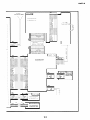
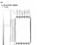
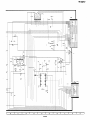
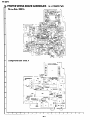
14. PRINTED WIRING BOARD ASSEMBLIES
14-1. POWER PWB
Wiring Side SIDE A
Component Side SIDE A
r
0904
‘TI
0922
Q921
RI925
cl
CN9G6
1
I
2
I
3
I
4
I
5
I
14-1
6
I
7
I
8
I
9
I
IO
I
VN-EZl U
Wiring Side SIDE B
Land at this position
from A
Component Side SIDE B
IO
I
11
I
12
I
13
I
14
I
14-2
15
I
16
I
17
I
18
I
19
VN-ET1 U
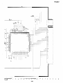
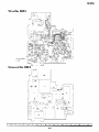
14-2. MAIN PWB
Wiring Side SIDE A
Component Side
IEI
m
lczrsl
F2151
m
C
M
!zEl
I
m
_I
\
.1/
piiiqET/
I--
(D
‘1
I
r-6
IC201
1
kl
i
I
1
14-3
VN-EZl U
B
Wiring Side
\
0
0
Component Side SIDE B
IC205
10
I
11
I
12
I
13
I
14
I T’@
I
n
I
14-4
15
I
16
I
17
I
18
I
19
VN-EttlJ
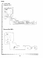
14-3. CONTROL PWB
Wiring Side SIDE A
Component Side SIDE A
TL@@
TL@p@
TL@P@
\
1
I
2
I
3
I
4
I
5
I
14-5
6
I
7
I
8
I
9
I
IO
Wiring Side SIDE B
Component Side SIDE B
IO
I
11
I
12
I
13
I
14
I
14-6
15
I
16
I
17
I
18
I
19
I
VN-EZl U
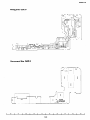
14-4. TFT PWB
Wiring Side SIDE A
Component Side SIDE A
Lj
IC802
I
J
pi-1
pm-1
C825
El
IC801
'JR804
Wiring Side SIDE B ,
Component Side SIDE B
P
Tl@
Tl@
Tl@
T@
/F&q
Tl@ Tt@
IO
I
11
I
12
I
13
I
14
I
14-8
15
I
16
I
17
I
18
I
19
VN-EZl U
14-5. CCD PWB
Wiring Side
SIDE A
Component Side
SIDE A
14-6. TILT PWB
Wiring Side
SIDE A
14-7. SHUTTER PWB
Wiring Side
SIDE A
Wiring Side
SIDE B
Component Side
Component Side
SIDE A
Wiring Side
SIDE B
Component Side
SIDE B
Component Side
Wiring Side
SIDE B
Component Side
SIDE B
14-8. JACK PW
1
I
2
Wiring Side SIDE A
Component Side SIDE A
Wiring Side SIDE B
Component Side SIDE B
I
3
I
4
I
5
I
6
I
7
I
8
I
9
I
10
1
VN-EZl U
15.REPLACEMENT PARTS LIST/
EXPLODED VIEWS
Ref. No.
Q922
Q924
Q925
Q926
Q927
Q928
Q929
Q930
VS2SD874ARl
E
VS2SD874A-RI E
VSDTCI 14YE/-1
VS2SA1362GR-1
VSDTCI 14YE/-1
VSDTCI 14YE/-1
VS2SA1362GR-1
VS2SA1362GR-1
VS2SA1314C/-1
D902
D903
D904
D905
D906
D907
0908
0913
D914
D917
D918
VHDI SS368N-1
VHDI SS368//-1
VHDFI AJ3///-1
VHDFI J2F/ll-1
VHDFI J2F///-1
VHDDA227///-1
VHDDA227///-1
VHDDAN222//-1
VHDI SS368//-1
VHDI SS368N-1
VHDI SS368N-1
L904
L905
L906
L907
L908
L909
L910
L911
L913
T901
T903
RCiLPO158TAZZ
RCiLPO158TAZZ
VPAXM2R2MR16N
VP-WM220KR71 N
VP-WM220KR71 N
VP-WM220KR71 N
VP-WM220KR71 N
VPAXMI OOKR42N
RCiLP0241 TAZZ
RTRNZOI 43TAZZ
RTRNZOI 45TAZZ
c901
c902
c903
c905
C906
c907
c910
c911
c913
c914
c915
C916
c917
C918
c921
c922
c923
c924
C926
c927
C928
c929
c930
c931
c932
c933
c934
c935
C936
c937
c939
c943
c944
C946
C948
c949
c950
C952
VCKYCY 1 EFI 042
VCKYCYI EFI 042
VCCCCZI EH201 J
VCKYCZI EB472K
VCCCCZIHHIOIJ
VCKYCZI HFI 032
VCKYCZI HBI 52K
VCKYCZI HBI 02K
VCKYTQI CBI 05K
VCKYCZI HBI 02K
VCKYTVI HF223Z
VCKYCZI CBI 03K
VCKYCYI EFI 042
VCKYTQI CBI 05K
RCKZO054TAZZ
RCKZO069TAZZ
RC-KZ0069TAZZ
RCKZO055TAZZ
RCKZOO72TAZZ
RCKZ0072TAZZ
RCKZ0069TAZZ
RCKZ0072TAZZ
RCKZ0072TAZZ
RCKZ0072TAZZ
RCKZ0072TAZZ
RCKZ0072TAZZ
RCKZOO72TAZZ
RCKZ0027TAZZ
RCKZ0069TAZZ
RCKZ0055TAZZ
RCKZ0055TAZZ
VCKYCYI EFI 042
RCKZ0027TAZZ
VCFREDI HM273J
RCKZ0389CEZZ
RCKZ0069TAZZ
RCKZ0069TAZZ
PC-KZOO69TAZZ
Q923
ELECTRICAL
PARTS
LIST
Parts marked with “A’ are important for maintaining the safety of the
set. Be sure to replace these parts with specified ones for maintaining
the safety and performance of the set.
Les pieces marquess ‘A’sont
importantes pour maintenir la securite
de l’appareii. Ne remplacer ces pieces que par des pieces dont le
numero est specific pour maintenir la securite et proteger le bon
fonctinnement
de I’appareil.
Contact your nearest SHARP Parts Distributor.
location of SHARP Parts Distributor,
Call Toll-free I-IBE800SHARP
in CANADA:
Contact SHARP Electronics of Canada Limited
Phone (416) 890-2100.
Description
Code
AD
AD
AB
AC
A0
AB
AC
AC
2SD874A
2SD874A
DTCI 14YE
2SA1362GR
DTC114YE
DTCI 14YE
2SA1362GR
2SA1362GR
2SA1314C
DIODES
uHOW TO ORDER REPLACEMENT PARTS.”
in USA:
*
Part No.
For
AC
AC
AE
AE
AE
AB
AB
AA
AC
AC
AC
1 SS368
1 SS368
Fl AJ3
Fl J2F
Fl J2F
DA227
DA227
DAN222
1SS368
1 SS368
1 SS368
COILS AND TRANSFORMERS
*MARK
: SPARE PARTS-DELIVERY
To have your order filled
the following informations.
promptly
1. MODEL NUMBER
3. PART NO.
5. PRICE CODE
A
A
SECTION:ALL
and correctly,
JAPAN
please
2. REF. NO.
4. DESCRIPTION
A
A
MARK: SAFETY RELATED PARTS
PIECES: RELATIV ‘ES A LA SECURITE
Part No.
*
Description
Code
PRINTED WIRING BOARD ASSEMBLIES
(NOT REPLACEMENT ITEM)
DUNTK2900QAOl
DUNTK2901QAOl
DUNTK2902PMOO
DUNTK2904QAOO
DUNTK2905PMOO
DUNTK2906PMOO
DUNTK2907PMOO
DUNTK2908PMOO
Power PWB Unit
Main PWB Unit
Control PWB Unit
TFT PWB Unit
CCD PWB Unit
Tilt PWB Unit
Jack PWB Unit
Shutter PWB Unit
-
DUNTK2900QAOl
POWER PWB UNIT
INTEGRATED CIRCUITS
IC901
IC903
IC904
IC905
IC906
VHiBA9708KV1
VHiXC62EP25-1
VHiXC62EP50-1
VHiXC62FP33-1
VHiTC7SH04U1
Q901
Q903
Q906
Q907
Q908
Q911
Q921
VSDTCI 14YE/-1
VSDTCI 15EUA-1
VS2SB1121 T/-l
VS2SB1121 T/-l
VS2SK2316//-1
VS2SA1314C/-1
VSSi6463DQ/-I
BA9708KV
XC62EP25
XC62EP50
XC62FP33
TC7SH04U
AM
AE
AE
AE
AE
TRANSISTORS
DTCI 14YE
DTCI ISEUA
2SB1121T
2SB1121T
2SK2316
2SA1314C
Si6463DQ
AE
AE
AC
AB
A0
AB
AB
AC
AF
AF
AM
CAPACITORS
PWB ASS IEMBLY IS NOT REPLACEMENT ITEM
L’ASSEMBLANGE P.C.I. EST UN ARTICLE NON REMPLACABLE
Ref. No.
Coil, CiLPO158TA
Coil, CiLPOl58TA
Peaking, 2.2pH
Peaking, 22pH
Peaking, 22pH
Peaking, 22yH
Peaking, 22p.H
Peaking, 1Op,H
Coil, CiLP0241 TA
Transformer
Transformer
AB
AB
AC
AC
AE
AD
AL
15-I
0.1
25V
0.1
25V
200~ 25V
4700~ 25V
loop
5ov
0.01
5ov
15oop 5ov
IOOOp 5ov
1
16V
IOOOp 5ov
0.022 5ov
0.01
16V
0.1
25V
1
16V
2.2
16V
IO
16V
IO
16V
3.3
16V
1
25V
1
25V
IO
16V
1
25V
1
25V
1
25V
1
25V
1
25V
1
25V
IO
16V
IO
16V
3.3
16V
3.3
16V
0.1
25V
IO
16V
0.027 50V
4kV
IO
IO
16V
16V
IO
IO
16V
Ceramic
Ceramic
Ceramic
Ceramic
Ceramic
Ceramic
Ceramic
Ceramic
Ceramic
Ceramic
Ceramic
Ceramic
Ceramic
Ceramic
Ceramic
Ceramic
Ceramic
Ceramic
Ceramic
Ceramic
Ceramic
Ceramic
Ceramic
Ceramic
Ceramic
Ceramic
Ceramic
Ceramic
Ceramic
Ceramic
Ceramic
Ceramic
Ceramic
Ceramic
Ceramic
Ceramic
Ceramic
AA
AA
AA
AB
AB
AB
AB
AB
AC
AB
AA
AB
AA
AC
AD
AE
AE
AD
AC
AC
AE
AC
AC
AC
AC
AC
AC
AF
AE
AD
AD
AA
AF
AD
AF
AE
AE
AE
VN-EZl U
Ref. No.
c954
c955
C956
*
Part No.
VCKYCZI HB221 K
VCKYCZl HB561 K
VCKYCZI AB104K
Description
220p
560~
0.1
50V Ceramic
50V Ceramic
1OV Ceramic
Code
AA
AC
AB
RESISTORS
VRS-TV1 JD332J
R901
VRS-CZI JF331 J
R902
VRS-CZI JFI 03J
R903
VRS-CZI JF223J
R904
VRS-CZI JFI 02J
R905
VRS-CZI JF103J
R906
VRS-CZI JFI 04J
R908
R909
VRS-CZl JF474J
VRS-CZI JFl53J
R910
VRS-CZI JF333J
R912
VRS-CZI JF333J
R913
VRS-CZl JF333J
R914
VRS-CZI JF474J
R915
VRS-CZI JF333J
R916
VRS-CZI JF124J
R917
VRS-CZI JF433J
R919
VRS-CZl JF333J
R920
R921
VRS-CZl JFI 05J
VRS-CZI JF684D
R922
VRS-CZI JF334D
R923
VRS-CZI JF39OJ
R924
VRS-CZl JFI 51 J
R925
R927
VRS-CZl JF39OJ
VRS-CZl JF433J
R928
VRS-CZI JF333J
R929
VRS-CZI JFI 02J
R931
VRS-CZI JFI 03J
R932
VRS-CZI JFI 01 D
R933
VRS-CZI JF223D
R934
VRS-CZI JF432D
R935
VRS-CZI JF153D
R936
VRS-CZI JFI 01 D
R937
VRS-CZI JFI 040
R938
VRS-CZl JF563D
R939
VRS-CZl JF473D
R940
VRS-CZI JF472D
R941
VRS-CZI JF623D
R942
VRS-CZl JF122D
R943
VRS-CZl JFl 01 D
R947
VRS-CZl JF273J
R949
VRSCZlJF15lJ
R950
VRS-CZI JF684J
R988
VRS-CZI JF334J
R989
VRS-CZI JF272J
R990
VRS-CZI JF473J
R993
VRS-CZI JF332J
R994
VRS-TV1 JD18OJ
R995
VRS-CZI JF223J
R996
VRS-CZI JFlO2J
R997
VRS-CZl JFI 04J
R1901
VRS-CZI JF224J
R1902
VRSCZlJF104J
R1903
VRS-CZl JFI 04J
RI 904
VRS-CZl JF474J
R1905
VRS-CZI JFI 04J
R1906
VRS-CZl JF104J
RI907
VRS-CZI JF273J
RI908
VRS-CZl JFOOOJ
R1911
VRS-CZI JFOOOJ
R1913
VRS-CZI JFOOOJ
RI914
VRS-CZI JF273J
R1916
VRS-CZI JFI 51 J
R1917
VRS-CZI JF273J
R1919
VRS-CZI JF102J
RI920
VRS-CZI JF273J
RI921
VRS-CZI JF471 J
R1922
VRS-CZI JFOOOJ
R1924
VRSTVlJD3R9J
R1925
VRS-CZI JFOOOJ
RI 926
3.3k l/l 6W
330 l/l 6W
1Ok l/l 6W
22k l/i 6W
lk
l/l 6W
1Ok. 1/I 6W
1OOk l/l 6W
470k l/l 6W
1 Sk l/l 6W
33k l/i 6W
33k l/i 6W
33k l/l 6W
470k l/l 6W
33k l/i 6W
120k l/l 6W
43k l/l 6W
33k l/l 6W
1 M l/i 6W
680k l/i 6W
330k l/l 6W
39
l/l 6W
150 l/i 6W
39
l/l 6W
43k l/l 6W
33k l/l 6W
lk
l/l 6W
1Ok l/i 6W
100 l/l 6W
22k l/l 6W
4.3k l/l 6W
1Sk l/l 6W
100 l/l 6W
1 OOk l/l 6W
56k l/l 6W
47k l/l 6W
4.7k l/l 6W
62k l/l 6W
1.2k 1/16W
100 l/l 6W
27k l/l 6W
150 l/l 6W
680k l/l 6W
330k l/l 6W
2.7k l/l 6W
47k l/l 6W
3.3k l/l 6W
18
l/l 6W
22k l/l 6W
lk
l/l 6W
1OOk l/l 6W
220k l/l 6W
1OOk l/l 6W
1OOk l/l 6W
470k l/l 6W
1OOk l/l 6W
1OOk l/l 6W
27k l/l 6W
l/l 6W
0
l/l 6W
0
l/l 6W
0
27k l/l 6W
150 l/l 6W
27k l/l 6W
l/l 6W
Ik
27k l/l 6W
470 l/l 6W
l/l 6W
0
3.9
l/l 6W
l/l 6W
0
Metal Oxide AA
Metal Oxide AA
Metal Oxide AA
Metal Oxide AA
Metal Oxide .AA
Metal Oxide AA
Metal Oxide AA
Metal Oxide AA
Metal Oxide AA
Metal Oxide AA
Metal Oxide AA
Metal Oxide AA
Metal Oxide AA
Metal Oxide AA
Metal Oxide AA
Metal Oxide AA
Metal Oxide AA
Metal Oxide AA
Metal Oxide AA
Metal Oxide AA
Metal Oxide AA
Metal Oxide AA
Metal Oxide AA
Metal Oxide AA
Metal Oxide AA
Metal Oxide AA
Metal Oxide AA
Metal Oxide AA
Metal Oxide AB
Metal Oxide AA
Metal Oxide AB
Metal Oxide AA
Metal Oxide AB
Metal Oxide AA
Metal Oxide AB
Metal Oxide AB
Metal Oxide AA
Metal Oxide AB
Metal Oxide AA
Metal Oxide AA
Metal Oxide AA
Metal Oxide AA
Metal Oxide AA
Metal Oxide AA
Metal Oxide AA
Metal Oxide AA
Metal Oxide AA
Metal Oxide AA
Metal Oxide AA
Metal Oxide AA
Metal Oxide AA
Metal Oxide AA
Metal Oxide AA
Metal Oxide AA
Metal Oxide AA
Metal Oxide AA
Metal Oxide AA
Metal Oxide AA
Metal Oxide AA
Metal Oxide AA
Metal Oxide AA
Metal Oxide AA
Metal Oxide AA
Metal Oxide AA
Metal Oxide AA
Metal Oxide AA
Metal Oxide AA
Metal Oxide AA
Metal Oxide AA
Ref. No.
*
Part No.
Desqiption
MISCELLANEOUS
CN901
CN905
CN906
CN907
CN909
FB901
FB902
FB903
FB904
FB906
FB907
FB908
FB909
FB910
FB911
FB912
FB913
A F901
A F902
A F903
A F904
A F905
PARTS
Plug, 2Pin
Connecting Cord, 3Pin
Socket, 30Pin
Socket, 13Pin
Plug, 5Pin
Balun, BLN-0049TA
Balun, BLN-0049TA
Balun, BLN-0049TA
Balun, BLN-0049TA
Balun, BLN-0049TA
Balun, BLN-0049TA
Balun, BLN-0049TA
Balun, BLN-0049TA
Balun, BLN-0049TA
Balun, BLN-0049TA
Balun, BLN-0049TA
Balun, BLN-0049TA
Fuse
Fuse
Fuse
Fuse
Fuse
QPLGN0263TAZZ
QCNW-1917TAZZ
QSOCZ3043CEZZ
QSOCNI 393TAZZ
QPLGN0564TAZZ
RBLN-0049TAZZ
RBLN-0049TAZZ
RBLN-0049TAZZ
RBLN-0049TAZZ
RBLN-0049TAZZ
RBLN-0049TAZZ
RBLN-0049TAZZ
RBLN-0049TAZZ
RBLN-0049TAZZ
RBLN-0049TAZZ
RBLN-0049TAZZ
RBLN-0049TAZZ
QFSL1721 TAZZ
QFSL1721TAZZ
QFSL1022TAZZ
QFS-L1022TAZZ
QFS-L1022TAZZ
Code
AB
AE
AG
AD
AC
AD
AD
AD
AD
AD
AD
AD
AD
AD
AD
AD
AD
AD
AD
AD
AD
AD
DUNTK290l QAOI
MAIN PWB UNIT
INTEGRATED CIRCUITS
IC31
IC33
IC34
IC35
IC201
IC202
IC203
IC204
IC205
IC206
IC601
IC602
VHiUPD1651 O-l
VHiXC62FP33-1
VHiVSP2000bl
VHiTC7WH04U1
RH-iX0700TAZZ
RH-iX0750TAZZ
RH-ix0701 TAZZ
VHiS80827LN-1
RH-iX0698TAZZ
VHiS24C04Abl
VHiNJM2113V1
VHiMSM7716/-1
Q201
Q601
Q602
Q603
Q604
Q605
Q652
Q653
VS2SC4081 RI-1
VSDTC114YEb1
VS2SAl362GR-1
VSDTCl14YEb1
VS2SAl362GR-1
VS2SAl362GR-1
VS2SC4213B/-1
VS2SC4081 R/-l
D201
0202
D601
VHDDAN222//-1
VHDDA221///-1
VHDDA221///-1
TM201
x201
VHHTI 103K44-1
RCRSCOI 54TAZZ
L31
L202
L203
L204
L205
L206
L207
L208
L210
L211
VP-WM2R2MR13N
VPAWMR47KR30N
VPAWMR47KR30N
VPAWMR47KR30N
VPAWMR47KR30N
VPAWMR47KR30N
VPAWMR47KR30N
VPAWMR47KR30N
VPAWMR47KR30N
VPAWMR47KR30N
UPD16510
XC62FP33
VSP2000
TC7WH04U
IX0700TA
IX0700TA
IX0701TA
S80827LN
IX0698TA
S24C04A
NJM2113V
MSM7716
AR
AE
AT
AE
BA
AV
BD
AE
AX
AL
AF
AT
TRANSISTORS
2SC4081 R
DTCI 14YE
2SA1362GR
DTCI 14YE
2SAl362GR
2SAl362GR
2SC4213B
2SC4081 R
AA
AB
AC
AB
AC
AC
AC
AA
DIODES
AA
AB
AB
DAN222
DA221
DA221
PACKAGED CIRCUITS
Thermistor
Crystal, CRSCOI 54TA
AD
AH
COILS
15-2
Peaking,
Peaking,
Peaking,
Peaking,
Peaking,
Peaking,
Peaking,
Peaking,
Peaking,
Peaking,
2.2pH
0.47pH
0.47pH
0.47pH
0.47pH
0.47pH
0.47yH
0.47pH
0.47pH
0.47yH
AB
AC
AC
AC
AC
AC
AC
AC
AC
AC
Vl\j-EZl U
*
Ref. No.
Part No.
c31
C32
c33
c34
c35
c37
C38
c39
c40
c41
C42
c43
c44
c45
C46
C48
c49
C51
c52
c53
c54
c55
C56
c57
C62
c201
c202
C203
C204
C205
C206
C207
C208
c209
c210
c211
c212
C213
C214
C215
C216
C217
C218
c219
c220
c221
c222
C223
C224
C225
C252
C253
C254
C255
C256
C601
C602
C603
C604
C605
C606
C610
C611
C650
C652
C653
C654
C656
C657
C658
VCKYCYI EF104Z
VCKYCYl EF104Z
VCKYTVI CF225Z
RC-KZOO84TAZZ
VCKYCil AFI 042
VCKYCYlCB104K
VCKYCZI AF104Z
VCKYCZI AFlO4Z
VCKYCZl AFI 042
VCKYCZl AFI 042
VCKYCZl AFI 042
VCSATAI AJI 06M
VCKYCZI AF104Z
VCKYCZI AFI 042
VCKYCZI AFI 042
VCSATAI AJI 06M
VCKYCZl AFlO4Z
VCKYCZI AFI 042
VCKYCZI AFI 042
VCCCCZl HHI OOD
VCCCCZl HHI OOD
VCKYCZI AFI 042
VCKYCY 1AFI 052
VCKYCY 1 AF105Z
VCCCCZI HHI 80J
VCCCCZl HHI OOD
VCCCCZI HH330J
VCKYCZl AFI 042
VCKYCZl AF104Z
VCSATAOJJI 56M
VCKYCZI AF104Z
VCKYCZI AFI 042
VCKYCZl AFI 042
VCKYCZl AFI 042
VCKYCZI AFlO4Z
VCKYCZI AFI 042
VCKYCZI AF104Z
VCKYCYI AFlO5Z
VCKYCYl AFI 052
VCKYCZl AFI 042
VCKYCZl AFI 042
VCKYCY 1AFI 052
VCKYCZI AFlO4Z
VCKYCZl AF104Z
VCSATAOJJI 56M
VCKYCY 1AF105Z
VCKYCYI AFlO5Z
VCKYCZI AFlO4Z
VCKYCZI AFI 042
VCKYCYl AFI 05Z
VCKYCZl AFI 042
VCKYCZl AFI 042
VCKYCZI AFI 04Z
VCKYCYlAF105Z
VCKYCYI AFI 052
VCSATAl AJ106M
VCKYCYl AFlO5Z
VCKYCZl AFlO4Z
VCSATAI CJ106M
VCKYCYI AFI 05Z
VCKYCZI AFI 042
VCKYCYI CB563K
VCKYCZI CBI 03K
VCSATEI AJ336M
VCSATElAJ336M
VCKYCZl AF104Z
VCKYCZI AFI 042
VCKYCZI AF104Z
VCKYCZl HB271 K
VCKYCY 1AF105Z
Description
Ref. No.
Code
CAPACITORS
.
-.
0.1
0.1
2.2
1
0.1
0.1
0.1
0.1
0.1
0.1
0.1
IO
0.1
0.1
0.1
10
0.1
0.1
0.1
IOP
25V
25V
16V
25V
1OV
16V
1 OV
1 OV
1OV
1OV
1OV
1OV
1 OV
1 OV
1 OV
1 OV
1OV
1OV
1OV
50V
1OP 50V
0.1
1 OV
1
1 OV
1
1 OV
50V
l8P
1OP 50V
50V
33P
0.1
1OV
0.1
1OV
15
6.3V
0.1
1OV
0.1
1 OV
0.1
1OV
0.1
1OV
0.1
1OV
0.1
1OV
0.1
1OV
1
1 OV
1
1 OV
0.1
1 OV
0.1
1OV
1
1OV
0.1
1OV
0.1
1 OV
15
6.3V
1
1 OV
1
1 OV
0.1
1OV
0.1
1 OV
1
1 OV
0.1
1 OV
0.1
1 OV
0.1
1OV
1
1 OV
1
1OV
10
1OV
1
1OV
0.1
1 OV
10
16V
1
1OV
0.1
1OV
0.056 16V
0.01
16V
33
1 OV
33
1OV
0.1
1OV
0.1
1OV
0.1
1OV
270~ 50V
1
1OV
Ceramic
Ceramic
Ceramic
Ceramic
Ceramic
Ceramic
Ceramic
Ceramic
Ceramic
Ceramic
Ceramic
Tantalum
Ceramic
Ceramic.
Ceramic
Tantalum
Ceramic
Ceramic
Ceramic
Ceramic
Ceramic
Ceramic
Ceramic
Ceramic
Ceramic
Ceramic
Ceramic
Ceramic
Ceramic
Tantalum
Ceramic
Ceramic
Ceramic
Ceramic
Ceramic
Ceramic
Ceramic
Ceramic
Ceramic
Ceramic
Ceramic
Ceramic
Ceramic
Ceramic
Tantalum
Ceramic
Ceramic
Ceramic
Ceramic
Ceramic
Ceramic
Ceramic
Ceramic
Ceramic
Ceramic
Tantalum
Ceramic
Ceramic
Tantalum
Ceramic
Ceramic
Ceramic
Ceramic
Tantalum
Tantalum
Ceramic
Ceramic
Ceramic
Ceramic
Ceramic
R37
R38
R39
R40
R41
R42
R44
R45
R20l
R202
R204
R205
R206
R207
R208
R209
R210
R211
R214
R215
R216
R217
R218
R219
R236
R237
R238
R241
R242
R243
R244
R245
R246
R248
R249
R251
R252
R253
R254
R255
R256
R257
R258
R259
R260
R261
R262
R263
R271
R272
R601
R602
R603
R604
R605
R606
R608
R609
R611
R615
R616
R621
R622
R623
R624
R650
R651
R653
R654
R655
R656
R657
R658
R659
AA
AA
AC
AC
AB
AB
AB
AB
AB
AB
AB
AC
AB
AB
AB
AC
AB
AB
AB
AB
AB
AB
AC
AC
AB
AB
AB
AB
AB
AC
AB
AB
AB
AB
AB
AB
AB
AC
AC
AB
AB
AC
AB
AB
AC
AC
AC
AB
AB
AC
AB
AB
AB
AC
AC
AC
AC
AB
AD
AC
AB
AB
AB
AG
AG
AB
AB
AB
AC
AC
RESISTORS
R31
R36
VRS-CZI JFI 03J
VRS-CZI JFI 02J
1Ok
Ik
l/l 6W
l/l 6W
Metal Oxide AA
Metal Oxide AA
15-3
Part No.
VRS-CZl JF102J
VRS-CZI JFI 02J
VRS-CZl JF102J
VRS-CZl JFI 02J
VRS-CZI JFI 02J
VRS-CZI JF102J
VRS-CZl JFOOOJ
VRS-CZl JFOOOJ
VRS-CZI JF561 J
VRS-CZI JF105J
VRS-CZl JF822J
VRS-CZI JF473J
VRS-CZl JFI 02J
VRS-CZI JFI 02J
VRS-CZl JF473J
VRS-CZI JF473J
VRS-CZl JF473J
VRS-CZI JFOOOJ
VRS-CZl JF473J
VRS-CZI JF473J
VRS-CZI JF822J
VRS-CZI JF473J
VRS-CZl JF473J
VRS-CZI JF473J
VRS-CZI JF272J
VRS-CZI JFI 22J
VRS-CZI JFI 52J
VRS-CZI JF473J
VRS-CZl JFOOOJ
VRS-CZI JF473J
VRS-CZl JF473J
VRS-CZlJF181J
VRS-CZl JF473J
VRS-CZI JF473J
VRS-CZl JF473J
VRS-CZI JF473J
VRS-CZI JFI 02J
VRS-CZI JF221 J
VRS-CZIJFIOIJ
VRS-CZI JFI 01 J
VRS-CZI JFI 01 J
VRS-CZI JFl 01 J
VRS-CZl JF473J
VRS-CZl JF473J
VRS-CZI JF473J
VRS-CZI JFOOOJ
VRS-CZl JFOOOJ
VRS-CY 1JFOOOJ
VRS-CZI JF561 J
VRS-CZl JF561 J
VRS-CZl JFI 53J
VRS-CZI JF332J
VRS-CZI JF104J
VRS-CZl JFI 03J
VRS-CZI JF153J
VRS-CZI JFI 02J
VRS-CZl JF564J
VRS-CZI JFI 02J
VRS-CZI JF473J
VRS-CZI JFI 02J
VRS-CZI JF273J
VRS-CZl JF273J
VRS-CZI JF273J
VRS-TV1 JD471 J
VRS-TV1 JD47l J
VRS-CZl JF682J
VRS-CZl JFI 01 J
VRS-CZI JF821 J
VRS-CZI JFI 53J
VRS-CZI JF222J
VRS-CZI JF102J
VRS-CZl JFI 04J
VRS-CZl JFI 53J
VRS-CZl JFOOOJ
*
Description
Ik
l/l 6W
Ik
l/l 6W
lk
l/l 6W
Ik
l/l 6W
Ik
l/l 6W
Ik
l/l 6W
0
l/l 6W
0
l/l 6W
560 l/l 6W
1M
l/l 6W
8.2k l/l 6W
47k l/l 6W
Ik
l/l 6W
Ik
l/l 6W
47k l/l 6W
47k l/l 6W
47k l/l 6W
0
l/l 6W
47k l/l 6W
47k l/l 6W
8.2k l/l 6W
47k l/l 6W
47k l/l 6W
47k l/l 6W
2.7k l/l 6W
1.2k l/l 6W
1.5k l/l 6W
47k l/l 6W
0
l/l 6W
47k l/l 6W
47k l/l 6W
180 l/l 6W
47k l/l 6W
47k l/l 6W
47k l/l 6W
47k l/l 6W
Ik
l/l 6W
220 l/l 6W
100 l/l 6W
100 l/l 6W
100 l/l 6W
100 l/l 6W
47k l/l 6W
47k l/l 6W
47k l/l 6W
0
l/l 6W
0
l/l 6W
0
l/l 6W
560 l/l 6W
560 l/l 6W
15k l/l 6W
3.3k 1/16W
1 OOk l/l 6W
1 Ok l/l 6W
15k l/l 6W
Ik
l/l 6W
560k l/l 6W
lk
l/l 6W
47k l/l 6W
Ik
l/l 6W
27k l/l 6W
27k l/l 6W
27k l/l 6W
470 l/l 6W
470 l/l 6W
6.8k 1/16W
100 l/l 6W
820 l/l 6W
15k l/l 6W
2.2k l/l 6W
Ik
l/l 6W
1 OOk l/l 6W
15k l/l 6W
0
l/l 6W
Metal Oxide
Metal Oxide
Metal Oxide
Metal Oxide
Metal Oxide
Metal ‘Oxide
Metal Oxide
Metal Oxide
Metal Oxide
Metal Oxide
Metal Oxide
Metal Oxide
Metal Oxide
Metal Oxide
Metal Oxide
Metal Oxide
Metal Oxide
Metal Oxide
Metal Oxide
Metal Oxide
Metal Oxide
Metal Oxide
Metal Oxide
Metal Oxide
Metal Oxide
Metal Oxide
Metal Oxide
Metal Oxide
Metal Oxide
Metal Oxide
Metal Oxide
Metal Oxide
Metal Oxide
Metal Oxide
Metal Oxide
Metal Oxide
Metal Oxide
Metal Oxide
Metal Oxide
Metal Oxide
Metal Oxide
Metal Oxide
Metal Oxide
Metal Oxide
Metal Oxide
Metal Oxide
Metal Oxide
Metal Oxide
Metal Oxide
Metal Oxide
Metal Oxide
Metal Oxide
Metal Oxide
Metal Oxide
Metal Oxide
Metal Oxide
Metal Oxide
Metal Oxide
Metal Oxide
Metal Oxide
Metal Oxide
Metal Oxide
Metal Oxide
Metal Oxide
Metal Oxide
Metal Oxide
Metal Oxide
Metal Oxide
Metal Oxide
Metal Oxide
Metal Oxide
Metal Oxide
Metal Oxide
Metal Oxide
Code
AA
AA
AA
AA
AA
AA
AA
AA
AA
AA
AA
AA
AA
AA
AA
AA
AA
AA
AA
AA
AA
AA
AA
AA
AA
AA
AA
AA
AA
AA
AA
AA
AA
AA
AA
AA
AA
AA
AA
AA
AA
AA
AA
AA
AA
AA
AA
AA
AA
AA
AA
AA
AA
AA
AA
AA
AA
AA
AA
AA
AA
AA
AA
AA
AA
AA
AA
AA
AA
AA
AA
AA
AA
AA
VN-EZl U
Ref. No.
Part No.
*
Description
MISCELLANEOUS
CN31
CN202
CN203
CN204
CN205
CN207
CN601
CN602
FB32
FB33
FB34
FB601
FB602
FB603
FB604
SC201
QSOCN 1393TAZZ
QSOCNI 086TAZZ
QPLGN0363TAZZ
QCNCW3082TAZZ
QCNW-191 STAZZ
QPLGN0474TAZZ
QPLGN0276TAZZ
QPLGN0263TAZZ
RBLN-0080TAZZ
RBLN-0080TAZZ
RBLN-0080TAZZ
RBLN-0081TAZZ
RBLN-0081 TAZZ
RBLN-0081 TAZZ
RBLN-0081 TAZZ
QSOCZ0056TAZZ
Ref. No.
Code
PARTS
Socket, 13Pin
Socket, 1OPin
Plug, 3Pin
Connector, 30Pin
Connecting Cord, 2Pin
Plug, 4Pin
Plug, 2Pin
Plug, 2Pin
Balun, BLN-0080TA
Balun, BLN-0080TA
Balun, BLN-0080TA
Balun, BLN-0081 TA
Balun, BLN-0081 TA
Balun, BLN-0081 TA
Balun, BLN-0081 TA
Socket, 26Pin
IC805
lC806
VHiTC7W14U/-1
VHiMB8346BV1
Q803
Q804
VS2SC4081 RI-I
VSDTC114EE/-1
0801
D802
VHDHVU359TR-1
VHDI SS368//-1
X801
RCRSC0087TAZZ
L801
L803
L804
L806
L805
L807
L808
VPAWM470J6R4N
VPAWM470J6R4N
VPAWM470J6R4N
VPAWM470J6R4N
VPMGNl OOMR75N
VPM6Nl OOMR75N
VP-9N330KR71 N
AH
VR804
RVR-M4553CEZZ
AC
C801
C802
C803
C804
C805
C806
C807
C808
C810
C811
C812
C813
C814
C815
C817
C818
C819
C821
C822
C823
C824
C825
C826
C827
C828
C830
C831
C832
C833
C834
C835
C836
C837
C839
C840
C841
C842
C843
C844
C845
C846
C848
C850
C851
C852
C853
C854
VCKYCZI HF103Z
VCKYCZI HFI 032
VCKYCZI HFlO3Z
VCKYCZI HFI 032
VCKYCZI HF103Z
VCKYCZI HFI 032
VCKYTQI CBI 05K
VCCCCYI HH471 J
VCKYCY 1AFI 052
VCSATAI CJ106M
VCKYCY 1AFI 05Z
VCKYCZI HFI 032
VCKYCY 1AFI 052
VCKYCZI HFI 032
VCKYCYI AF105Z
VCKYCZl HF103Z
VCKYCZI HFI 032
VCCCCZI HH560J
VCKYCYI AFI 052
VCCCCZI HHGROD
VCKYCY 1AFI 052
VCKYTVl CB474K
VCKYCZI HFI 032
VCKYCZI HF103Z
VCSATAI AJ106M
VCKYCZI HFI 032
VCKYCYl CF334Z
VCCCCZI HH270J
VCCCCZlHH150J
VCKYCZI HFI 032
VCKYCZI HF103Z
VCKYCZl HF103Z
VCSATAlAJ106M
VCSATAI CJ106M
VCSATAl AJ106M
VCKYCZI HF103Z
VCKYCZI HFI 032
VCSATAI AJ106M
VCKYCYI EFI 042
VCKYCYI EFI 042
VCSATAl AJI 06M
VCKYCZI HFI 032
VCCCCYI HH561 J
VCKYCZI AFI 042
VCKYCY 1AFI 052
VCKYCY 1AFI 05Z
VCKYCZl HBI 02K
AD
AC
AC
AF
AE
AD
AD
A0
.AC
AC
AC
A0
A0
A0
AB
AM
D2901
VHDRB451 F//-l
X2901
RCRSC0032TAZZ
C2901
C2902
C2903
C2904
C2905
C2906
RCDZ0004TAZZ
VCCCCZI HHSROD
VCCCCZI HHSROD
VCKYCZlAF1042
VCKYCZI HB102K
VCKYCZI HB102K
R2901
R2902
R2903
R2904
R2905
R2906
R2907
R2908
R2909
R2910
R2911
R2912
R2915
VRS-CZI
VRS-CZl
VRS-CZI
VRS-CZl
VRS-CZl
VRS-CZI
VRS-CZI
VRS-CZI
VRS-CZI
VRS-CZI
VRS-CZI
VRS-CZl
VRS-CZI
CN2901
SW2901
SW2902
SW2903
SW2905
SW2906
SW291 0
SW291 1
QSOCNl078TAZZ
QSW-K0026TAZZ
QSW-KOO26TAZZ
QSW-K0026TAZZ
QSW-K0026TAZZ
QSW-K0026TAZZ
QSW-S0203TAZZ
QSWS0204TAZZ
Crystal, CRSCOO87TA
AK
Peaking,
Peaking,
Peaking,
Peaking,
Peaking,
Peaking,
Peaking,
47pH
47pH
47pH
47pH
1OpH
1OpH
33pH
AC
AC
AC
AC
AC
AC
AD
Variable Resistor
AC
CAPACITORS
RB451 F
Crystal, CRSC0032TA
AG
CAPACITORS
Capacitor
9p
50V
9p
50V
0.1
1OV
IOOOp 50V
IOOOp 50V
AK
AA
AA
AB
AB
A0
Ceramic
Ceramic
Ceramic
Ceramic
Ceramic
RESISTORS
22k
22k
5.6k
5.6k
12k
12k
56k
56k
47
22k
5.6k
12k
lk
MISCELLANEOUS
l/l
It1
l/l
l/l
l/l
l/l
l/l
l/l
l/l
l/l
l/l
l/l
l/l
6W
6W
6W
6W
6W
6W
6W
6W
6W
6W
6W
6W
6W
Metal
Metal
Metal
Metal
Metal
Metal
Metal
Metal
Metal
Metal
Metal
Metal
Metal
Oxide
Oxide
Oxide
Oxide
Oxide
Oxide
Oxide
Oxide
Oxide
Oxide
Oxide
Oxide
Oxide
AB
AB
AB
AB
AA
AA
AA
AA
AA
AB
AB
AA
AA
PARTS
Socket,
Switch,
Switch,
Switch,
Switch,
Switch,
Switch
Switch
1OPin
Left
Menu
Up
Down
Right
AD
AC
AC
AC
AC
AC
AD
AF
DUNTK2904QAOO
TFT PWB UNIT
INTEGRATED
AE
AC
HVU359TR
1 SS368
COILS
PACKAGED CIRCUIT
VHiiR3Y29AM-1
VHiNJM4565V1
AA
AB
2SC4081 R
DTCI 14EE
PACKAGED CIRCUIT
DIODE
IC801
IC802
AG
AN
TC7W14U
MB8346BV
CONTROL
S3530A
JF223D
JF223D
JF562D
JF562D
JFI 230
JFI 230
JF563D
JF563D
JF47OJ
JF223D
JF562D
JF123D
JFI 02J
Code
DIODES
INTEGRATED CIRCUIT
VHiS3530A//-1
Description
TRANSISTORS
DUNTK2902PMOO
CONTROL PWB UNIT
IC2901
*
Part No.
CIRCUITS
IR3Y29AM
NJM4565V
AV
AF
15-4
0.01
0.01
0.01
0.01
0.01
0.01
1
470~
50V
50V
50V
50V
50V
50V
16V
50V
1
1OV
IO
16V
1
1OV
0.01
50V
1
1OV
0.01
50V
1
1OV
0.01
50V
0.01
50V
50V
56P
1
1OV
50V
6P
1
1OV
0.47
16V
0.01
50V
0.01
50V
10
1OV
0.01
50V
0.33
16V
50V
27P
50V
15P
0.01
50V
0.01
50V
0.01
50V
IO
1OV
10
16V
1OV
IO
0.01
50V
0.01
50V
10
1OV
0.1
25V
0.1
25V
10
1OV
0.01
50V
560~ 50V
0.1
1OV
1
1OV
1
1OV
1OOOp50V
Ceramic
Ceramic
Ceramic
Ceramic
Ceramic
Ceramic
Ceramic
Ceramic
Ceramic
Tantalum
Ceramic
Ceramic
Ceramic
Ceramic
Ceramic
Ceramic
Ceramic
Ceramic
Ceramic
Ceramic
Ceramic
Ceramic
Ceramic
Ceramic
Tantalum
Ceramic
Ceramic
Ceramic
Ceramic
Ceramic
Ceramic
Ceramic
Tantalum
Tantalum
Tantalum
Ceramic
Ceramic
Tantalum
Ceramic
Ceramic
Tantalum
Ceramic
Ceramic
Ceramic
Ceramic
Ceramic
Ceramic
AB
AB
A0
AB
AB
AB
AC
AA
AC
AD
AC
AB
AC
AB
AC
AB
AB
AB
AC
AA
AC
AC
AB
AB
AC
A0
AA
AB
AB
AB
AB
AB
AC
AD
AC
AB
A0
AC
AA
AA
AC
AB
A%
A0
AC
AC
A0
VN-EZl U
Ref. No.
Part No.
C855
C856
C857
C858
C859
C860
C861
C862
C863
C864
VCCCCYlHHlSlJ
VCCCCYI HH561 J
VCCCCYI HH221 J
VCSATAI AJ335M
VCKYCZl HFI 032
VCCCCZI HH8ROD
VCKYCZI AFI 042
VCKYCZI HFI 032
VCCCCZI HH560J
VCCCCZI HH820J
R801
R803
R804
R806
R807
R808
R809
R812
R813
R815
R816
R817
R818
R819
R820
R821
R822
R823
R824
R826
R827
R828
R829
R830
R832
R833
R834
R835
R836
R837
R838
R839
R840
R841
R842
R844
R852
R854
R857
R858
R859
R860
R861
R862
R882
R886
R887
R888
R889
R891
R892
R893
VRS-CZI JF333D
VRS-CZl JF393D
VRS-CZI JF203D
VRS-CZl JFI 02J
VRS-CZI JFI 530
VRS-CZI JFI 030
VRS-CZI JF473D
VRS-CZl JFI 02J
VRS-CZl JFI 02J
VRS-CZI JFI 05J
VRS-CZI JF333D
VRS-CZI JF433D
VRS-CZI JFI 830
VRS-CZI JF222D
VRS-CZI JF272D
VRS-CZI JF334J
VRS-CZI JF183D
VRS-CZI JF562J
VRS-CZI JF393D
VRS-CZI JF822J
VRS-CZI JFI 05J
VRS-CZl JF333D
VRS-CZI JF393D
VRS-CZI JFI 830
VRS-CZI JF223D
VRS-CZl JFI 530
VRS-CZI JF223D
VRS-CZI JF561 D
VRS-CZI JFOOOJ
VRS-CZI JF472D
VRS-CZI JFI 540
VRS-CZI JFI 04J
VRS-CZI JFOOOJ
VRS-CZI JFI 540
VRS-CZl JF473J
VRS-CZI JFI 81 J
VRS-CZI JFI 03J
VRS-CZlJF181J
VRS-CZl JF202J
VRS-CZI JFI 04J
VRS-CZI JF332J
VRS-CZI JF472J
VRS-CZI JFI 81 J
VRS-CZI JF39l J
VRS-CZI JF472J
VRS-CZI JFI 03J
VRS-CZI JFI 03J
VRS-CZI JF103J
VRS-CZl JFI 03J
VRS-CZI JF154J
VRS-CZI JFI 540
VRS-CZI JFI 03J
CN802
CN803
QSOCN2687TAZZ
QSOCNI 393TAZZ
*
Code
Description
150p
560~
220p
3.3
0.01
8P
0.1
0.01
56P
82P
33k
39k
20k
Ik
15k
10k
47k
Ik
Ik
1M
33k
43k
18k
2.2k
2.7k
330k
18k
5.6k
39k
8.2k
IM
33k
39k
l8k
22k
15k
22k
560
0
4.7k
150k
IOOk
0
150k
47k
180
10k
180
2k
IOOk
3.3k
4.7k
180
390
4.7k
10k
10k
10k
IOk
150k
150k
10k
MISCELLANEOUS
5ov
5ov
5ov
IOV
5ov
5ov
IOV
5ov
5ov
5ov
Ceramic
Ceramic
Ceramic
Tantalum
Ceramic
Ceramic
Ceramic
Ceramic
Ceramic
Ceramic
1/16W
1/16W
1/16W
1/16W
1/16W
1/16W
1/16W
1/16W
1/16W
1/16W
1/16W
1/16W
1/16W
1/16W
1/16W
1/I 6W
1/16W
1/16W
1/16W
1/16W
1/16W
1/16W
1/16W
1/16W
1/16W
1/16W
1/16W
1/16W
ll16W
1/16W
1/16W
1/16W
1/16W
1/16W
1/16W
1/16W
1/16W
1/16W
1/16W
1/16W
l/l 6W
1/I 6W
1/16W
1/16W
1/16W
1/16W
1/16W
1/16W
1/16W
1/16W
1/16W
1/16W
Metal
Metal
Metal
Metal
Metal
Metal
Metal
Metal
Metal
Metal
Metal
Metal
Metal
Metal
Metal
Metal
Metal
Metal
Metal
Metal
Metal
Metal
Metal
Metal
Metal
Metal
Metal
Metal
Metal
Metal
Metal
Metal
Metal
Metal
Metal
Metal
Metal
Metal
Metal
Metal
Metal
Metal
Metal
Metal
Metal
Metal
Metal
Metal
Metal
Metal
Metal
Metal
Oxide
Oxide
Oxide
Oxide
Oxide
Oxide
Oxide
Oxide
Oxide
Oxide
Oxide
Oxide
Oxide
Oxide
Oxide
Oxide
Oxide
Oxide
Oxide
Oxide
Oxide
Oxide
Oxide
Oxide
Oxide
Oxide
Oxide
Oxide
Oxide
Oxide
Oxide
Oxide
Oxide
Oxide
Oxide
Oxide
Oxide
Oxide
Oxide
Oxide
Oxide
Oxide
Oxide
Oxide
Oxide
Oxide
Oxide
Oxide
Oxide
Oxide
Oxide
Oxide
Ref. No.
DUNTK2905PMOO
CCD PWB UNIT
AA
AB
AA
AC
AB
AB
AB
AB
AB
AB
INTEGRATED CIRCUIT
ICl
VHiLZOP3641-1
Ql
VS2SC2404-C-1
01
VHDI SS368//-1
Cl
c3
c4
c5
C6
C8
c9
Cl0
Cl1
VCKYCYlEF1042
VCCCCYl HH271 J
VCSATEI VJ225M
VCSATEI VJ225M
VCKYCZI HFI 032
VCKYTQl HB224K
VCKYTQI HB224K
VCKYCZI CB103K
VCCCCZlHH180J
RI
R2
R3
R5
R7
R8
RIO
RI1
VRS-CZl JF105J
VRS-CZIJFIOIJ
VRS-CZI JF392J
VRS-CZl JFI 01 J
VRS-CZIJFIOIJ
VRS-CZI JFI 01 J
VRS-CZI JFI 01 J
VRS-CZI JFI 05J
CNI
QSOCN 1305TAN 1
BH
LZOP3641
TRANSISTOR
AD
2SC2404-C
DIODE
AB
AB
AA
AA
AB
AB
AB
AA
AA
AA
AB
AA
AB
AA
AB
AA
AB
AA
AB
AA
AA
AB
AB
AB
AB
AB
AB
AA
AA
AB
AB
AA
AA
AB
AA
AA
AA
AA
AA
AA
AA
AA
AA
AA
AA
AA
AA
AA
AA
AA
AB
AA
AC
1 SS368
CAPACITORS
0.1
270~
2.2
2.2
0.01
0.22
0.22
0.01
18P
25V
50V
35V
35V
50V
50V
50V
16V
50V
Ceramic
Ceramic
Tantalum
Tantalum
Ceramic
Ceramic
Ceramic
Ceramic
Ceramic
AA
AA
AD
AD
AB
AC
AC
AB
AB
Metal
Metal
Metal
Metal
Metal
Metal
Metal
Metal
AA
AA
AA
AA
AA
AA
AA
AA
RESISTORS
1M
100
3.9k
100
100
100
100
1M
MISCELLANEOUS
l/l
l/l
l/l
l/l
l/l
l/l
l/l
l/l
6W
6W
6W
6W
6W
6W
6W
6W
Oxide
Oxide
Oxide
Oxide
Oxide
Oxide
Oxide
Oxide
PART
AF
Socket, 13Pin
DUNTK2906PMOO
TILT PWB UNIT
MISCELLANEOUS
CN1201 QCNW-1922TAZZ
SW1201 QSW-M0032TAZZ
PARTS
Connecting Cord, 3Pin
Switch
AE
AE
DUNTK2907PMOO
JACK PWB UNIT
RESISTOR
RI 923
VRS-TX2HFOOOJ
CN908
J901
SW901
QCNW-1917TAZZ
QJAKE0171 CEZZ
QSW-MOO18TAZZ
0
MISCELLANEOUS
1/2W
Metal Oxide
AA
PARTS
Connecting Cord, 3Pin
Jack
Switch
AE
AD
AC
DUNTK2908PMOO
SHUTTER PWB UNIT
PARTS
Socket, 26Pin
Socket, 13Pin
Description
Part No.
MISCELLANEOUS
AE
AD
CN206
SW294
15-5
QCNW-191 STAZZ
QSW-K0027TAZZ
PARTS
Connecting Cord, 2Pin
Switch, Shutter
AE
AD
VN.IEZ~ U
Ref. No.
Part No.
*
Description
Code
Ref. No.
SUPPLIED ACCESSORIES
CDSKAO032TAOl
CDSKA0039TAOl
GCASN0022TAZZ
RUNTK0350TAZZ
TiNSE0345TAZZ
TiNSE0346TAZZ
TiNSE0352TAZZ
UADP-0243TAZZ
UBNDTOIOITAZZ
SmartMedia
CD ROM
Soft Case
Floppy Disk Adapter
Operation Manual
(For Main Unit)
Operation Manual
(For ROM)
Operation Manual
(For Flash Calipers)
AC Adapter
Hand Strap
BF
AM
AU
BV
AG
AD
AE
BB
AG
PACKING PARTS
(NOT REPLACEMENT ITEM)
SPAKA631 GTAZZ
SPAKA6317TAZZ
SPAKA6333TAZZ
SPAKC7445TAZZ
SPAKPGI 22TAZZ
SPAKPGI 25TAZZ
Packing Add. (Top)
Packing Add.(Bottom)
AC Adapter Add.
Packing Case
Polystylene Sack
Pat
-
SERVICE JIG
QCNW-1948TAZZ
QCNW-1949TAZZ
QCNW-1950TAZZ
Main PWB (CN204)BS
Power PWB (CN906), 30Pin
Main PWB (CN202)AP
Control PWB (CN2901), IOPin
Power PWB (CN907)AP
TFT PWB (CN803), 13Pin
CABINET PARTS
1
1-2
I-3
1-4
I-5
1-6
1-7
I-8
l-9
I-10
l-11
l-12
1-13
1-14
CCABA6211 TAK2
GCOVAI 617TAKA
GCOVAI 620TAKA
JBTN-0307TASA
TCAUH0235TAZZ
TLABZ0500TAZZ
PZETV0407TAZZ
CSLiFOOl ITAOI
‘GFTAB1073TAKA
LHLDZ1507TAZZ
MSPRPOI 95TAFN
LANGK0522TAFW
MSPRPOI 99TAFN
PZETV0409TAZZ
1-15
2
2-2
2-3
2-4
2-5
2-6
2-7
2-8
2-9
2-10
2-11
2-12
PSPAZ0282TAZZ
CCABB6211 TAKl
JKNBZ0075TASA
GCOVAI 618TAKA
CCOVAI 619TAKl
JKNBPO180TASA
JKNBP0181TASA
JKNBZ0074TASA
MSPRCO123TAFJ
LHLDZI 506TAZZ
LHLDZ1516TAZZ
LHLDZ3041TAZZ
RMiCC0087TAZZ
Front Cabinet Ass’y
AR
Front Grip
AG
Top Cover
AD
Shutter Button
AE
Battery Label
AA
POP Label
AG
Electrostatic Sheet( Shutter) AB
Slider, Complete
AK
Battery Lid
AG
Battery Terminal Holder
AD
Battery Terminal Spring
AD
Battery Terminal Block Base AC
Battery Terminal B
AD
Electrostatic Sheet
AA
(Fulcrum Fitting)
Spacer A
AA
AX
Back Cabinet Ass’y
Menu Knob
Back Grip Cover
AG
Speaker Cover Ass’y
AF
Power Button
AC
Change Knob
AC
Cursor Knob
AE
Return Knob Spring
AB
Speaker Holder
AD
Bearing Holder
AC
Tripod Base Holder
AE
Microphone Unit
AL
15-6
Part No.
*
2-13
2-14
VSPOO2OP-968N
PZETV0408TAZZ
2-15
2-16
2-17
2-18
2-19
3
3-1
3-3
3-4
PSPAZ0303TAZZ
PSPAZ0304TAZZ
PSPAZ0296TAZZ
PSPAZ0283TAZZ
PSPAZ0308TAZZ
CHLDB1031TAOl
LANGK0475TAFW
LHLDBI 032TAZZ
LHLDZ1508TAZZ
3-5
3-6
3-7
3-8
3-9
3-10
3-11
31
31-1
31-2
31-3
31-4
31-5
31-6
31-7
39
40
41
42
43
44
45
46
47
48
49
50
51
71
72
73
74
75
76
77
78
79
80
81
82
83
84
85
87
88
89
90
A
B
C
D
E
F
G
H
i
K
L
M
N
LHLDZ3037TAFN
MSPRPOI 97TAFN
MSPRPOI 98TAFN
QCNW-1918TAZZ
PSPAZ0301 TAZZ
PSPAZ0302TAZZ
PSPAZO282TAZZ
CANGF0346TAOl
LANGF0346TAFW
LHLDZ1512TAZZ
LHLDZ1513TAZZ
LHLDZ1514TAZZ
LPLTM0031 TAFW
MSPRPOI 96TAFW
QPWBH2903TAZZ
LANGK0478TAFW
LHLDZ1515TAZZ
GCABB6212TAKA
JKNBPOI 82TASA
JKNBZ0076TASA
LHLDZI 51 OTAZZ
MLEVF0022TAFF
PFiLZ0009TAZZ
PFiLZOOl OTAZZ
GCABA6212TAKA
CSLDM3339TAOl
TCAUHO238TAZZ
TLABM2008TAZZ
DUNTK2908PMOO
DUNTK2904QAOO
DUNTK2901QA02
DUNTK290OQAOl
DUNTK2907PMOO
DUNTK2906PMOO
DUNTK2905PMOO
DUNTK2902PMOO
VHiLZOP3641-1
RLCDV0050TAZZ
QCNW-1920TAZZ
QCNW-1924TAZZ
QPWBH291 GTAZZ
LANGK0521 TAFW
PSPAZ031 ITAZZ
PSPAZ0298TAZZ
TCAUS0554TAZZ
TLABH0359TAZZ
PSPAZ0312TAZZ
LX-BZ021 OTAFN
LX-HZOO56TAFN
LX-HZ0058TAFF
LX-HZ0062TAFF
LX-HZ0055TAFF
LX-BZ0208TAFF
LX-BZ0206TAFN
LX-BZO208TAFN
LX-NZ3053GEZZ
LX-WZ0054TAOO
LX-WZOOS1TAO2
LX-WZ0053TAOO
LX-HZ0057TAFC
Description
Code
Speaker
AL
Electrostatic Sheet
AB
(Tripod Spring)
AA
Battery Spacer C
Battery Spacer D
AB
Spacer B
Speaker Spacer
AA
Mic Spacer
Battery Case/Frame Ass’y AR
Cabinet Angle
AC
Battery Holder
Reverse Connection
Prevention Spacer
AD
Strap Holder
AD
Battery Terminal +AD
Battery Spring
AD
Power Connector
AA
Battery Spacer A
AB
Battery Spacer B
AA
Spacer A
AU
Tilt Ass’y
AG
Tilt Frame Ass’y
AD
Tilt Holder
AC
Cam Ring
AC
Wire Holder
AB
Plate
AB
Click Spring
AG
CCD FPC
AC
Macro ring Angle
AD
Macro Adjusting Ring
Camera Rear Cabinet
AH
AD
ND Knob
AE
Ring
AD
Knob Holder
AD
Macro Adjusting Lever
AD
Filter
AH
Lens Cover
AH
Camera Front Cabinet
AH
LCD Shield Plate
AA
Label
AC
Model Label
Shutter PWB Unit
TFT PWB Unit
Main PWB Unit
Power PWB Unit
Jack PWB Unit
Tilt PWB Unit
CCD PWB Unit
Control PWB Unit
BH
CCD Sensor
BQ
LCD
AE
Connectior
AD
Flat Cable
AB
Flexible PWB
Cabinet Fastening Angle A AE
Cabinet Filler Spacer
AB
Shutter Spacer
AB
UL Caution Label
AB
AB
FCC Label
Battery Lid Spacer
AC
AA
Screw
AA
Screw
Screw
AA
Screw
AA
Screw
AA
AA
Screw
Screw
AA
Screw
AA
AC
Nut
Washer
AB
Washer
AA
Washer
AA
Screw
AA
1
I
2
I
3
I
4
I
5
I
6
1
16. PACKING OFTHE SET
GCASN0022TAZZ
Soft Case
RUNTK0350TAZZ
Floppy Disk Adapter
I
I
CDSKA0039TAOl
CD ROM
*SPAKA6316TAZZ
Packing Add. (Top)
TiNSE0345TAZZ
\
Operation Manual
\
(For Main Unit)
\
TiNSE0346TAZZ
Operation Manual
(For ROM)
\
\
4
TiNSE0352TAZZ
Operation Manual
(For Flash Calipers)
UBNDTOIOITAZZ
Hand Strap
/
I=+=-
-
CDSKA0032TAOl
SmartMedia
* SPAKPGI 22TAZZ
Polyethelene Sack
UADP-0243TAZZ
AC Adapter
ItSPAKP6125TAZZ
Pat
* SPAKA6333TAZZ
AC Adapter Add.
* SPAKA6317TAZZ
Packing Add.( Botto
* Not Replacement item
16-1
SHARP
COPYRIGHT
@ 1999 BY SHARP CORPORATION
ALL RIGHTS RESERVED.
No part of this publication may be reproduced,
stored in a retrieval system, or transmitted in
any form or by any means, electronic, mechanical,
photocopying,
recording, or otherwise, without
prior written permission of the publisher.
Jul. 1999
TQ0683-S
Printed in JAPAN
SA. NS
SHARP CORPORATION
AV Systems Group
Quality & Reliability Control Center
Yaita, Tochigi 329-2193, Japan