1
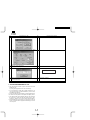
SERVICE MANUAL
MODEL
UP-700
SRV Key : LKGIM7113RCZZ
PRINTER : PR-58HM
(For "U & A" version)
CONTENTS
CHAPTER 1. SPECIFICATIONS ................................................................1 - 1
CHAPTER 2. OPTIONS ..............................................................................2 - 1
CHAPTER 3. SERVICE PRECAUTION ......................................................3 - 1
CHAPTER 4. SRV. RESET AND MASTER RESET ....................................... 4 - 1
CHAPTER 5. DIAGNOSTICS SPECIFICATIONS.......................................5 - 1
CHAPTER 6. CIRCUIT DESCRIPTION ......................................................6 - 1
CHAPTER 7. TCP/IP I/F PWB DESCRIPTION...........................................7 - 1
CHAPTER 8. CIRCUIT DIAGRAM ..............................................................8 - 1
CHAPTER 9. PWB LAYOUT.......................................................................9 - 1
Parts marked with " " are important for maintaining the safety of the set. Be sure to replace these parts with specified
ones for maintaining the safety and performance of the set.
SHARP CORPORATION
This document has been published to be used
for after sales service only.
The contents are subject to change without notice.
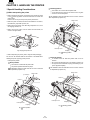
CHAPTER 1. SPECIFICATION
2) KEY TOP NAME
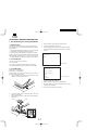
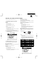
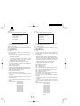
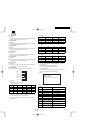
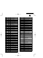
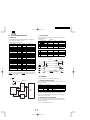
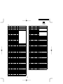
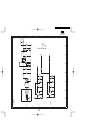
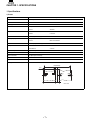
1. APPEARANCE
Standard key top
External view
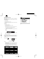
KEY TOP
0-9,00,000
Front view
Customer display
(Pop-up type)
Journal cover
DESCRIPTION
Numeric keys
Decimal Point key
Operator display
CL
Contrast control
@/FOR
Power switch
RECEIPT
Receipt paper feed key
JOURNAL
Journal paper feed key
Receipt paper
Mode switch
Keyboard
Drawer
PAGE UP
PAGE DOWN
CANCEL
Drawer lock
Clear key
Multiplication key
Page up key
Page down key
Cancel key
Cursor keys
Rear view
ENTER
Enter key
RFND
Refund Key
SERV#
Server code entry key
RCPT
Receipt print Key
TAX SHIFT
VOID
PLU/SUB
Power switch
(D-PLU) 1 to 100
Tax 1 shift key
Void Key
PLU/SUB dept./UPC code entry key
Direct PLU 1 to 100 keys
Rear cover
P.SHIFT#
AUTO1, 2
MISC FUNC
2. RATING
CONV#
External dimensions :
With a drawer
445 (W) x 485 (D) x 312 (H) mm
Weight : With a drawer 16.4kg
10%, 60Hz
Power source
120V AC
Power consumption
Stand-by : 16 W
Operating : 57 W (max.)
Working temperatures
0 to 40 °C
CH#
Charge Menu Key
SBTL
Subtotal Key
CA/AT
Cash / amount tendered key
FINAL
Tentative finalization key
GLU
RECEIPT JOURNAL
87
88
89
90
91
92
93
94
95
96
97
98
99
71
72
73
74
75
76
77
78
79
80
81
82
83
84
85
86
58
59
60
61
62
63
64
65
66
67
68
69
70
MISC
FUNC
AUTO
1
AUTO
2
48
49
50
51
52
53
54
55
56
57
38
39
40
41
42
43
44
45
46
47
SERV
#
28
29
30
31
32
33
34
35
36
37
PAGE
UP
18
19
20
21
22
23
24
25
26
PAGE
27 DOWN
9
10
11
12
13
14
15
16
17
1
2
3
4
5
6
7
RCPT
ENTER
8
*1 Note:
August Production:
The [Auto 2] Key will be the [NC] Key.
VOID
100
RFND CANCEL LEVEL CONV
#
#
@
TAX
SHIFT
8
CL
9
P-SHIFT
7
PLU/
SUB
GLU
4
5
6
CHK
#
SRVC
1
2
4
00
0 000
FOR
#
CH
#
FINAL
SBTL
CA/AT
*1
Currency conversion menu key
Check Menu Key
SRVC
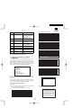
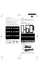
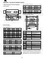
1) STANDARD KEYBOARD LAYOUT
Automatic sequencing 1 and 2 keys
Miscellaneous function key
CHK#
LEVEL#
3. KEYBOARD
Price shift menu key
PLU level shift menu key
Service key
Guest Look-up key
>>>>> USE FONT <<<<<
Helvetica/ Helvetica-Condensed/ Century-Schoolbook/ Symbol & OriginalFonts: (RingWorld2/RingFont2/Pa
Symbol/PartsCod)
- - - - - - - - - - - - - - - - - - - - - - - - - - - - - - - - - - - - - - - - - - - - - - - - - - - - - - -
Optional key top
KEY TOP
(D-PLU) 101 to 123
(Dept) 1 to 99
DESCRIPTION
Direct PLU 101 to 123 Keys
Department 1 to 99 Keys
KEY TOP
GDSC %1 to %3
DESCRIPTION
Group discount %1 to 3 keys
COVER CNT
Cover count key
New check key
%1 to 5
Percent 1 to 5 keys
N.C
(-)1 to 5
Discount 1 to 5 keys
C_NEXT
Condiments next key
CH1 to 9
Charge 1 to 9 keys
EDIT TIP
Edit tip key
CASH#
FUNC. MENU
RP SEND
Cash menu key
Function menu key
Remote printer send key
GRT EX
Gratuity exempt key
CA2 to 5
Cash 2 to 5 keys
CONV1 to 4
Conversion 1 to 4 keys
RA1 to 2
Received-on-Account 1 and 2 keys
PO1 to 2
Paid out key 1 and 2 keys
AUTO3 to 25
CHK1 to 5
RP ROUND
PLU MENU1 to 50
MACRO1 to 4
UPSIZE
CAP.1 to 10
GLU RECALL
Repeat round key
PLU menu 1 to 50 keys
Macro 1 to 4 keys
Upsize key
Data capture 1 to 10 keys
Table # recall key
MSG1 to 5
Message 1 to 5 keys
MSG#
Message menu key
Automatic sequencing 3 and 25 keys
DELETE
Delete key
Check 1 to 5 keys
NEXT $
Next higher dollar key
P1 to 6
Price level shift 1 to 6 keys
MDSE SBTL
Merchandise subtotal key
LEVEL1 to 5
Menu level shift 1 to 5 keys
TRAY SBTL
Tray subtotal key
FS SHIFT
Food stamp shift key
FS TEND
Food stamp tender key
GD1 to 3 SHIFT
CASH TIP
CHARGE TIP
TIP PAID
EAT IN1 to 3
TAX2 to 4 SHIFT
NS
SCALE
OPEN TARE
RTN
GAS SBTL
Return key
Gasoline sales subtotal key
Group discount shift 1 to 3 keys
AMT
Amount entry key
Cash tip key
#/TM
Non-add code / Date & Time display key
Charge tip key
Tip paid key
Eat in 1 to 3 keys
Tax 2 to 4 shift keys
No sale key
Scale entry key
Tare entry key
REPEAT
IND. PAYMENT
INQ
CUST
PRICE CHANGE
BIRTH
TABLE #
Repeat key
Individual payment key
Inquiry key
Customer code entry key
UPC price change key
Birthday entry key
Table no. (seat no.) entry key
BAL
Balance key
VOID MENU
Void menu key
DEPOSIT
Deposit key
RFND SALE
Refund sale key
DEPOSIT RF
DEPT#
Deposit refund key
Department number key
TAX
Manual tax key
BACL SPACE
Back space key
TRANS OUT
Transfer out key
TRANS IN
Transfer in key
RCP SW
Receipt ON/OFF key
WASTE
Waste mode key
BS
Bill separation key
BT
Bill totalize / bill transfer key (CHECK-ADD)
PRINT
Validation print key
BILL
Bill print key
PAST VOID
Past void key
SBTL VOID
Subtotal void key
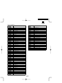
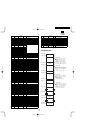
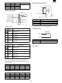
3) TEST PROGRAMMING KEY SHEET LAYOUT
[
RECEIPT JOURNAL
]
Ñ
_
-
”
+
¿
{
}
,
?
<
>
!
@
#
$
%
^
&
(
)
=
Q
W
E
R
T
Y
U
I
O
P
/
A
S
D
F
G
H
J
K
L
:
Z
X
C
V
B
N
M
,
;
.
(DC)
(SHIFT)
4) BLANK KEY SHEET LAYOUT
RECEIPT JOURNAL
(DEL)
(INS)
(CANCEL) (RECALL)
@
FOR
¥ CL
PAGE
UP
7
8
9
PAGE
DOWN
4
5
6
(ENTER)
1
2
3
00
0 000
(UPDATE)
SBTL
CA/AT
: The shaded area contains the character keys which are
used for programming characters.
KEY TOP
DESCRIPTION
SHIFT
Used for programming characters.
Entering upper-case letters
You can enter an upper-case letter by using this
key. Press this key just before you enter the
upper-case letter. You should press this key each
time you enter an upper-case letter.
DC
Used for programming characters.
Entering double-size characters
This key toggles the double-size character mode
and the normal-size character mode. The default
is the normal-size character mode. When the
double-size character mode is selected, the letter
"W" appears at the bottom of the display.
INS
Used for programming characters.
To select a text editing mode
Toggles between the insert mode ("_") and the
overwrite mode ("■").
DEL
Used for programming characters.
To delete a character or figure
Deletes a character or figure in the cursor position.
BACK SPACE Used for programming characters.
To delete a character or figure
Backs up the cursor for deleting the character or
figure at the left of the cursor. When your POS
terminal is in the insert mode, this key deletes the
character or the value at the cursor position.
Used to move the cursor.
ENTER
Used to program each setting.
TL
Used to finalize programming.
CANCEL
Used to cancel programming and to get back to
the previous screen.
PREV
RECORD
Used to go back to the previous record, e.g. from
the department 2 programming window back to
the department 1 programming window.
NEXT
RECORD
Used to go to the next record, for example, in
order to program unit prices for sequential
departments.
PAGE DOWN
PAGE UP
CL
Used to scroll the window to go to the next page.
Used to scroll the window to go back to the
previous page.
Used to clear the last setting you have
programmed or clear the error state.
Used to toggle between two or more options.
SBTL
RECALL
Numeric keys
Used to list those options which you can toggle by
the [ ] key.
Used to call up a desired code.
Used for entering figures.
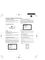
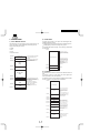
3. DISPLAY
1) OPERATOR DISPLAY
• Screen example 1 (REG mode)
Server code
Scroll guidance:
Mode name
When a transaction information
occupies more than 5 lines, scroll
key(s) appears to indicate you can
scroll to the direction.
Status area 1:
Sales information
area:
Sales information
you have just entered
such as items and
prices will appear
between 2nd line and
6th line.
Total is always appear
at 7th line.
Status area 2:
Time
Numeric entry
Price level shift indicator
(P1-P6)
: Shows the PLU/UPC price level
currently selected.
PLU level shift indicator
(L1-L5)
: Shows the PLU level currently selected.
Receipt shift indicator (r)
: Shows the receipt shift status.
Stock alarm indicator ( ! )
: Appears when the stock of the PLU
which you entered is zero, negative
or reaches the minimum stock.
Electronic message indicator (M)
: Appears when an electronic message is received. (Status 1 area)
Receipt ON/OFF status indicator (R)
: Appears when the receipt ON-OFF
function signs OFF.
Sentinel mark (X)
: Appears in the lower right corner of
the screen when the cash in drawer
exceeds a programmed sentinel
amount.
The sentinel check is performed for
the total cash in drawer.
• Screen example 2 (PGM mode)
4. KEYS AND SWITCHES
Programming item
information area
1) MODE SWITCH AND MODE KEYS
MA
Programming area:
Programmable items
are listed.
SM
REG
OP X / Z
0.24 (W) x 0.21 (H) mm
Dot space
0.02 mm
Dot color
White
Back color
Dark blue
• Operator key (OP)
• Service key (SRV)
SRV
Dot size
SM
320(W) x 240(H) Full dot
• Submanager key (SM)
• Manager key (MA)
OP
LCD display
Dot format
X2/Z2
PGM2
MA
Device type
X1 /Z1
PGM1
Screen save mode
When you want to save the electric power or save the display’s life,
use the screen save function. This function can turn the LCD off when
a server does not operate the POS terminal for an extended period of
time. You can program the time for which your POS terminal should
keep the normal status (in which the backlight is "ON") before it goes
into the screen save mode.
To go back to the normal mode, press any key.
MGR
OFF
The mode switch has these settings:
OFF:
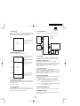
2) DISPLAY ADJUSTMENT (OPERATION DISPLAY)
You can adjust the contrast of the display by using the contrast
control, and also you can adjust the display angle. Pull up the tab, the
display will head up.
OP X/Z: This setting allows cashiers/clerks to take X or Z reports for
their sales information. (This setting may be used only
when your register has been programmed for "OP X/Z
mode available" in the PGM2 mode.)
REG:
For entering sales
PGM1:
To program those items that need to be changed often:
e.g., unit prices of departments, PLUs or UPCs, and percentages
PGM2:
To program all PGM1 items and those items that do not
require frequent changes: e.g., date, time, or a variety of
register functions
MGR:
For manager’s and submanager’s entries
The manager can use this mode to make entries that are
not permitted to be made by cashiers/servers -for example,
after-transaction voiding and override entry.
X1/Z1:
To take the X/Z report for various daily totals
X2/Z2:
To take the X/Z report for various periodic (weekly or
monthly) consolidation
Tab
Contrast control
Turning the control backwards
darkens the display and
turning it forwards lightens the
display.
The backlight in the display is a consumable part.
When the LCD display may no longer be adjusted and becomes
darker, you should change the backlight.
3) CUSTOMER DISPLAY (Pop-up-type)
This mode locks all register operations.
No change occurs to register data.
2) DRAWER LOCK KEY
This key locks and unlocks the drawer. To lock it, turn 90 degrees
counterclockwise. To unlock it, turn 90 degrees clockwise.
SK1-2
Double-size character mode
indicator (W):
Appears when the double-size
character mode is
selected during text programming.
Caps lock indicator
(A/a):
The upper-case letter “A”
appears when caps lock is on,
and the lower-case letter “a”
appears when caps lock is off
during text programming.
4) PRINTER COVER LOCK KEY
This key locks and unlocks the printer cover. To lock it, turn 90
degrees counterclockwise. To unlock, turn 90 degrees clockwise.
5. PRINTER
1) PRINTER (PR-58HA)
Item
Description
No. of station
2: Receipt and Journal
Validation
No
Printing system
Line thermal
No. of dot
Receipt:
360 dots
Journal
360 dots
Horizontal:
0.125 mm
Vertical:
0.125 mm
Dot pitch
Font
Printing capacity
10 dots (W) x 24 dots (H)
Receipt:
Max. 30 characters
Journal:
Max. 30 characters
Character size
1.25 mm (W) x 3.0 mm (H):
At 10 x 24 dots
Print pitch
Column distance:
1.5 mm
Row distance:
3.75 mm
Paper feed speed
Approximate 65 mm/s
Reliability
Mechanism:
Paper end sensor
Yes (Receipt and Journal)
Cutter
Manual
Paper near end sensor
No
MCBF 5 milion lines
Printing area
106(848dots)
(7.0)
(5.5)
360dots
(45)
0.125
(5.5)
57.5 ±0.5
5.0
(7.0)
UNIT: mm
Item
Description
Printing format
12 x 24 font
1.5 (12dots)
3.0 (24dots)
0.125
3.75 (30dots)
3.75 (30dots)
0.125
1.5 (12dots)
UNIT: mm
2) PAPER
Item
Name
Roll dimension
Thickness
2) MONEY CASE
Description
Heat-quality paper
57.5 0.5 mm in width
0.06 mm to 0.08 mm
6. DRAWER
Separation from the drawer
Allowed
Separation of the coin
compartments from the money case
Bill separator
Number of compartments
U version
Allowed
A version
Allowed
Disallowed
Disallowed
No
7B/5C
Standard (1 pcs)
4B/8C
Bill separator
1) SPECIFICATION
(1) Drawer box and drawer
Model name
Size
Color
Material
Bell
Release lever
Drawer open sensor
SK-460
445 (W) x 464 (L) x 118 (H)
GRAY 368
Metal
—
Standard equipment; Front key
Standard equipment
U version : 7B/5C
A version : 4B/8C
3) LOCK
Location of the lock
Front
Method of locking
and unlocking
Locking:
Insert the drawer lock key into
the lock and turn it 90 degrees
counterclockwise.
Unlocking:
Insert the drawer lock key into
the lock and turn it 90 degrees
clockwise.
Key No.
SK1-2
7. RS232 INTERFACE
This machine has two RS232 standard ports for communication to PC, Hand scanner (ER-A6HS1) and etc.
1) PORT 1 (CH1) (CN402)
2) PORT2 (CH2) (CN403)
Connector type: D-SUB 9pin
Data rate: max. 38,400 bps
Connector type: Modular jack RJ45 8pin
Data rate: max. 115,200 bps
1
/CD
1
/RS
2
RD
2
/ER
3
SD
3
SD
4
/ER
4
5
GND
6
/DR
7
/RS
8
/CS
/CI
VCC(+5V)
S401
5
GND
6
RD
7
/DR
8
/CS
CI
CD
S404
S403
VCC
(+5V)
GND
9
3) OPTIONAL DEVICES THAT CAN BE CONNECTED
Standard port
Option port (ER-A5RS)
Port No.
Port1: CH1
Port2: CH2
Port3:
Port4:
Type
D-SUB 9pin
Moduler RJ45
D-SUB 9pin
D-SUB 9pin
CI/+5V selectable
–
–
–
ER-A6HS1 (+5V necessary)
–
–
–
–
–
Scanner (+5V not necessary)
Modem
–
PC
Printer, Scale
POS utility, 02fd.exe
–
The ER-A6HS1 cannot be connected to port 2, 3 or 4 because it
requires +5V.
The modem cannot be connected to port 2 because it uses a
different signal line.
For the modular RJ45 to D-Sub 9pin conversion cable, see the
following.
Moduler RJ45
CI
CD
S404
S403
GND
VCC
(+5V)
D-sub 9pin
/RS
1
7
/RS
/ER
2
4
/ER
SD
3
3
SD
4
1
/CD
GND
5
5
GND
RD
6
2
RD
/DR
7
6
/RS
/CS
8
8
/CS
9
/CI
(Open)
Pole Display
<Option>
UP-P16DP
Remote
Drawer
<Option>
ER-03DW/
04DW
Expansion
memory
board
<Option>
UP-S02MB
UP-S04MB
INLINE Communication
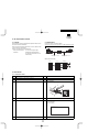
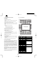
1. SYSTEM CONFIGURATION
CHAPTER 2. OPTIONS
Master machine
MCR
<Option>
UP-E13MR
RS-232 Board
ER-A5RS
<Option>
Std. 2/
Max.4 ports
RS-232 Communication
(Ethernet)
Coin Dispenser
<Local purchase>
CAT Terminal
<Local purchase>
Scale
<Local purchase>
Hand Scanner
ER-A6HS1
Laser Scanner
<Local purchase>
PC
<Local purchase>
PC
<Local purchase>
Remote printer/Slip
<Local purchase>
Satellite machines
Max 63 units
(Batch communications)
>>>>> USE FONT <<<<<
Helvetica/ Helvetica-Condensed/ Century-Schoolbook/ Symbol & OriginalFonts: (RingWorld2/RingFont2/Pa
Symbol/PartsCod)
- - - - - - - - - - - - - - - - - - - - - - - - - - - - - - - - - - - - - - - - - - - - - - - - - - - - - - -
2. SALES OPTIONS
No.
1
CLASSIFICATION
COMPONENT NAME
Memory
Expansion RAM board
MODEL NAME
REMARK
UP-S02MB
2M bytes PS-RAM board
UP-S04MB
4M bytes PS-RAM board
2
Display
Remote display (Pole type)
UP-P16DP
11-Dig.7-Seg. + 16-Dig.Dot
3
Drawer
Remote drawer
ER-03DW
7B/5C coin case
ER-04DW
5B/5C coin case
4
On-line function
RS232 I/F board
5
Card reader
MCR (Magnetic Card Reader)
UP-E13MR
ER-A5RS
6
Scanner
Bar code hand scanner
ER-A6HS1
2 ports RS232 I/F
ISO Type 1 : 3 stripe card
3. LOCAL PURCHASE OPTIONS
No.
COMPONENT NAME
1
External printer
2
Slip printer
3
Scale I/F
4
Coin dispenser
5
Color kitchen monitor
6
CAT terminal
MODEL NAME
REMARK
TM-T88/85, TM-88 (2), TM-T80
TM-U200, TM-300
TM-295
1: Please consult with your Sharp regional sales manager.
4. SERVICE OPTIONS
No.
NAME
PARTS CODE
PRICE
1
Mode key grip cover
AX
2
Drip proof mode switch cover
BA
DESCRIPTION
For MA key only
5. SERVICE TOOLS
No.
NAME
PARTS CODE
PRICE
DESCRIPTION
1
Service key
AF
2
RS232 Loop Back Connector
BC
For RS232 D-SUB 9pin connector
3
RS232 modular Loop Back Connector
BC
For RS232 RJ45 Modular jack connector
4
Expansion PWB for option board
BU
For ER-A5RS
5
MCR test card
BL
For UP-E13MR
6. SUPPLIES
No.
NAME
PARTS CODE
PRICE
DESCRIPTION
1
Thermal roll paper
BA
5 Rolls / pack
2
Thermal roll paper (High preservative type)
BD
5 Rolls / pack
3
Key sheet (Normal key layout)
AR
4
Key sheet (Character key layout)
AH
5
Key sheet (Blank key layout)
AG
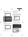
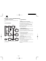
7. HOW TO USE SERVICE TOOLS
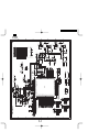
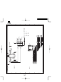
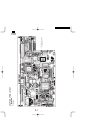
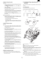
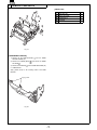
1) EXPANSION PWB : CKOG-6708RCZZ
• External view
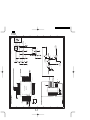
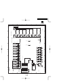
2) MCR TEST CARD : UKOG-2357RCZZ
• Used when executing the diagnostics of the UP-E13MR.
• External view
Purpose 1 : Used for servicing and repairing of options (such as the
ER-A5RS) which are connected with the main body option connector.
[Procedure 1]
Use an insulator base as shown in the shaded section when performing servicing.
UP-700
Main PWB
Loop back connectors
UKOG-6705RCZZ
Expansion PWB
(CKOG-6708RCZZ)
ER-A5RS
PWB
Base
A
To check the option I/F PWB from the solder side, connect the I/F
PWB to OPTCN2. To check from the parts side, connect to OPTCN3.
(Note) The option I/F PWB should be held horizontally so that no
excessive stress is applied to connecting section .
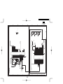
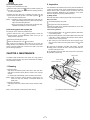
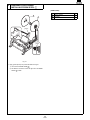
[Procedure 2]
Pop up
String
UP-700
Main PWB
Loop back connectors
UKOG-6705RCZZ
Expansion PWB
(CKOG-6708RCZZ)
ER-A5RS
PWB
Control ROM
Put a string between the pop up and the option PWB. Adjust the
length of the string so that the CKOG-6708RCZZ and the option PWB
are not binding. Once verified, then you may proceed with performing
service.
CHAPTER 3. SERVICE PRECAUTION
1. IPL (Initial Program Loading) FUNCTION
1) INTRODUCTION
4.
Place the mode key to any position except OFF or SRV’.
The application software of the UP-700 is written in the flash ROM.
In the following cases, writing of the application software into the flash
ROM is required.
5.
Turn on the power switch of the UP-700.
6.
The following display is shown and the IPL procedure is started.
When the procedure is completed, the message of "Completed"
is shown.
• When the flash ROM is replaced with a new one. The service part
flash ROM does not include the application software in it.
• When IPL writing is required because of a change in the software.
IPL from PROM
The service part of the main PWB unit includes the flash ROM with
the application software written in it, and there is no need for
writing the application software when replacing the main PWB unit.
Version check…
Erase …
2) IPL PROCEDURE
There are two ways for the IPL procedures.
• IPL from P-ROM
• IPL from PC communication (Please refer to the next section)
IPL write start
The detailed descriptions on the above procedures are given below.
26 27 28 29 2A 2B
3) IPL FROM P-ROM
2C 2D 2E 2F 30 31
Master ROM-1 : VHI27801RAU1A
Master ROM-2 : VHI27801RAV1A
32 33 34 35 36 37
38 39 3A 3B 3C 3D
Before installation, turn off the power switch on the UP-700 and unplug the AC cord from the AC outlet.
1.
3E 3F
Insert a screwdriver into the slit on the right side of the lower
cabinet to remove the option RAM case.
Verify …
IPL write completed
Completed.
7.
Turn off the power switch of UP-700.
8.
Remove the ROMs IC sockets on the IPL ROM PWB.
9.
IPL switch (SW301) on the IPL ROM PWB: Set the IPL switch
(SW301) to the OFF position.
10. Perform one of the master reset procedures.
2.
IPL switch (SW301) on the IPL ROM PWB: Set the IPL switch
(SW301) to ON position.
3.
Install the ROMs into the IC sockets on the IPL ROM PWB as
shown below.
ROM1
ROM2
ROM1
on
SW301
off
ROM2
>>>>> USE FONT <<<<<
Helvetica/ Helvetica-Condensed/ Century-Schoolbook/ Symbol & OriginalFonts: (RingWorld2/RingFont2/Pa
Symbol/PartsCod)
- - - - - - - - - - - - - - - - - - - - - - - - - - - - - - - - - - - - - - - - - - - - - - - - - - - - - - -
2. UP-700 UTILITY TOOLS
1) OUTLINE
2) CONNECTION
This Specification document describes the explanation about "POSUTILITYTOOL.EXE and "02FD.EXE".
PC and UP-700 are connected by RS232.
Connect the CH2 port of the UP-700 to the RS-232 interface of the
PC.
"POSUTILITYTOOL.EXE"and "02FD.EXE" works on Windows 95/98
of PC and they have the following
Functions by connecting UP-700 with RS232.
POSUTILITYTOOL.EXE
: IPL of UP-700 Program Object
02FD.EXE
: All RAM Data Upload/Download
(PC software tool instead of the current ER-02FD.)
UP-700:CH2
PC
D-SUB 9pin - D-SUB 9pin
cable
D-SUB 9pin - modular RJ-45
conversion cable
RS232 Cable Connecting:
[PC]
D-sub 9pin
SD
GND
RD
[UP-700]
Moduler RJ45
D-sub 9pin
7
4
3
1
5
2
6
8
9
7
4
3
1
5
2
6
8
9
/RS
/ER
SD
/CD
GND
RD
/DR
/CS
/CI
7
4
3
1
5
2
6
8
9
1
2
3
4
5
6
7
8
/RS
/ER
SD
GND
RD
/DR
/CS
(Open)
CI
CD
S404
S403
VCC
(+5V)
3) PROCEDURE
3) -1. POS UTILITY TOOL
No
1
Procedure on P.C. side
No
Procedure on UP-700 side
Install "POSUTILITYTOOL.EXE" on the P.C.
2
Turn OFF the power.
3
Select "IPL Mode".
Set the "IPL Switch" (SW302) of the UP-700 to "ON".
on
off
on
off
SW302
4
Turn ON the power.
5
Starting of "IPL Mode".
The UP-700 displays.
"IPL from Serial I/O"
IPL from Serial I/O
6
Connect the P.C. and the UP-700 (CH2) via RS232. (Fig 1)
GND
No
Procedure on P.C. side
7
Execute the "POSUTILITUTOOL.EXE" on the P.C.
*Please close all other applications while using this utility.
8
Select the ROM object Files by clicking the "Add Files.." button.
9
Push the "SEND" button.
Program data is sent to the UP-700 automatically.
No
9
Procedure on UP-700 side
Program data is received from P.C. automatically.
The UP-700 display.
IPL from serial I/O
Connected IRDA 115200
21 22 23 24 25 26 27 28
10
When data sending is completed,
the initial Window is shown after "Complete" window.
10
The UP-700 displays
"Completed."
IPL from Serial I/O
Connected IRDA 115200
21 22 23 24 25 26 27 28
29 2A 2B 2C 2D 2E 2F
Completed.
IPL from Serial I/O
Connected IRDA 115200
30 31 32 33 34 35 36 37
38 39 3A 3B 3C 3D 3E 3F
Completed.
11
Turn OFF the power.
12
Select "Normal Mode".
Set the "IPL switch" to "OFF".
(Ref. Hardware manual)
13
Execute the "Service Reset" on UP-700.
3) -2. 02FD
No
1
2
Procedure on P.C. side
Install the "02FD.EXE" on the P.C.
ALL RAM Data UpLoad : Go to "2"
ALL RAM Data DownLoad : Go to "9"
ALL RAM Data UpLoad
Connect the P.C. and the UP-700 (CH2) via RS232. (Fig 1)
No
2
3
Procedure on UP-700 side
Enter the SRV mode.
Select " 2 SETTING ".
Select " 14 BACKUP SEND"
displays
BACKUP SEND
SEND DATA
ALL RAM
SPEED
4
Execute the "02FD.EXE" on the P.C.
*Please close all other apprications while using this utility.
5
Set the Communication method by pushing the "Setting" Button.
6
7
Push the "OK" Button.
Push the "Receive Start" Button.
And Select the Receiving File.
Communication starts.
7
PROGRAMMED SPEED
Push CA/AT key. The UP-700 displays
SENDING
8
9
The UpLoad is completed.
The initial Window is shown.
Push the "Exit" Button.
ALL RAM Data UpLoad
Connect the P.C. and the UP-700 (CH2) via RS232. (Fig 1)
00000
8
The UpLoad is completed.
The SETTING menu is shown.
9
Enter the SRV mode.
Select " 2 SETTING".
Select " 15 BACKUP RECEIVE"
The UP-700 shows
10
BACKUP RECEIVE
SPEED
Push the CA/AT key.
PROGRAMMED SPEED
No
11
Procedure on P.C. side
Execute the "02FD.EXE" on the P.C.
*Please close all other apprications while using this utility.
12
Set the Communication method by pushing the "Setting" Button.
13
14
Push the "OK" Button.
Push the "Transmit Start" Button.
And Select the Sending File.
Communication starts.
No
14
Procedure on UP-700 side
The UP-700 displays
RECEIVING
15
The DownLoad is completed.
The initial Window is shown.
Push the "Exit" Button.
3. NOTE FOR HANDLING OF LCD
• The LCD elements are made of glass. Use extreme care when
handling the LCD.
Any strong shock applied to the LCD can cause damage.
• If the LCD element is broken and the liquid has leaked, do not
come in contact with it. If the liquid is attached to your skin or cloth,
immediately clean with soap.
• Use the unit under the rated conditions to prevent against damage.
• Be careful not to drop water or other liquids on the display surface.
• The reflection plate and the polarizing plate are easily scratched.
Be careful not to touch them with hard objects such as glass,
tweezers etc. Never hit, push, or rub the surface with hard objects.
• When installing the unit, be careful not to apply stress to the LCD
module. If excessive stress is applied, abnormal display or uneven
color may result.
00000
15
DownLoad is completed.
The SETTING menu is shown.
16
Execute the " Service Reset " on the UP-700
CHAPTER 4. SRV. RESET AND MASTER RESET
The SRV key is used for operating in the SRV mode.
MRS-2 (Master resetting 2)
Used to clear all memory and keyboard contents.
1. SRV. RESET (Program Loop Reset)
This reset returns all programming back to defaults. The keyboard
must be entered by hand.
This reset is used if an application needs a different keyboard layout
other than that supplied by a normal MRS-1.
Procedure
• Method 1
1) Turn off the AC switch.
Procedure
2) Set the mode switch to (SRV’) position.
1) Turn off the AC switch.
3) Turn on the AC switch.
2) Set the MODE switch to the (SRV’) position.
4) Turn to (SRV) position from (SRV’) position.
3) Turn on the AC switch.
• Method 2
1) Set the mode switch to PGM2 position.
2) Turn off the AC switch.
3) While holding down the JOURNAL FEED key and RECEIPT
FEED keys, turn on the AC switch.
Note: When disassembling and reassembling always power up using method 1 only. Method 2 will not reset the CKDC9.
Note: SRV programming job#926-B must be set to a "4" to allow the
PGM program loop reset.
4) While holding down the JOURNAL FEED and RECEIPT FEED
keys, turn to the (SRV) position from the (SRV’) position.
5) Key position assignment:
After the execution of a MRS-2, only the RECEIPT FEED and
JOURNAL FEED keys can remain effective on key assignment.
Any key can be assigned on any key position on the main keyboard.
[key setup procedure]
MRS-2 executed
0
Key position set
*2
Free key
0
PRG. RESET
*1
Free key setup
complete.
Disable
MASTER RESET
NOTES:
*1: When the 0 key is pressed, the key of the key number on the
display is disabled.
*2: Push the key on the position to be assigned. With this, the key of
the key number on the display is assigned to that key position.
*3: When relocating the keyboard, the PGM 1/2 modes use the
standard key layout.
2. MASTER RESET (All memory clear)
There are three possible methods to perform a master reset.
MRS-1 (Master resetting 1)
Used to clear all memory contents and return the machine back to its
initial settings.
Return the keyboard back to the default layout.
Procedure
1) Turn off the AC switch.
2) Set the MODE switch to the (SRV’) position.
3) Turn on the AC switch.
4) While holding down the JOURNAL FEED key, turn to the
(SRV) position from the (SRV’) position.
Key
No.
001
002
003
004
005
006
007
008
009
010
Key
name
Key
No.
011
012
013
014
015
016
017
018
019
020
Key
name
Key
No.
021
022
023
Key
name
>>>>> USE FONT <<<<<
Helvetica/ Helvetica-Condensed/ Century-Schoolbook/ Symbol & OriginalFonts: (RingWorld2/RingFont2/Pa
Symbol/PartsCod)
- - - - - - - - - - - - - - - - - - - - - - - - - - - - - - - - - - - - - - - - - - - - - - - - - - - - - - -
MRS-3 (Master resetting 3)
Master resetting 3 requires the entry of Serial No. data in addition to
Master resetting 2.
After completion of the MRS-3, the following operations and programming will be inhibited.
1. GT programming.
2. All memory download via RS-232.
3. GT resets with Z report. (Z report can be made, but the GT will not
be reset.)
Procedure
1) Turn off the AC switch.
2) Set the reset switch to the "SRV" position.
3) Turn on the AC switch.
4) While holding down the JOURNAL FEED key and MRS-3 key,
turn to the (SRV) position from the (SRV’) position.
MRS-3 key : UP-700=[PLU72] key
5) The product serial No. input window is displayed as shown
below.
DISPLAY:
SERIAL No.
00000000
Enter the product serial No. of this POS and enter the [CA/AT]
key.
6) Key position assignment:
After the execution of MRS-2, only the RECEIPT FEED and
JOURNAL FEED keys can remain effective on key assignment.
Any key can be assigned on any key position on the main keyboard.
[key setup procedure]
MRS-2 executed
0
Key position set
*2
Free key
0
*1
Free key setup
complete.
Disable
MASTER RESET
NOTES:
*1: When the 0 key is pressed, the key of the key number on the
display is disabled.
*2: Push the key on the position to be assigned. With this, the key of
the key number the on display is assigned to that key position.
*3: When relocating the keyboard, the PGM 1/2 modes use the
standard key layout.
Key
No.
001
002
003
004
005
006
007
008
009
010
Key
name
Key
No.
011
012
013
014
015
016
017
018
019
020
Key
name
Key
No.
021
022
023
Key
name
CHAPTER 5. DIAGNOSTICS SPECIFICATIONS
1. GENERAL DESCRIPTION
This Diag Program consists of a number of Diag. programs for the
UP-700, which facilitate the PWB check, process check and the operation check of the system during servicing.
The Service Diag. programs are all contained in the standard ROM.
2) RAM & ROM & SSP DIAGNOSITCS
This program tests the standard RAM, expanded RAM, standard and
service ROMs, and SSp circuit. RAM&ROM&SSP is selected on the
MAIN MENU, the following sub-menu screen appears. The cursor
shown in reverse video can be moved using the up/down arrow keys.
Move the cursor to the menu item you want and press the ENTER
key to execute the corresponding program. Press the CANCEL key to
return the screen to this submenu.
2. SYSTEM COMPOSITION
RAM&ROM&SSP DIAG
Standard RAM Check
UP-700 only
UP-S04MB Check
UP-S02MB Check
Standard ROM Check
UP-700
Service ROM Check
SSP Check
Fig 2-1. Service
2)-1. Standard RAM check
3. DIAG.
Checking
Starting the Diag. Program
The program performs the following checks on the standard
512KB of RAM. Data in memory remains unchanged before and
after the checks.
The Diag. Program is written on the external ROM, which is executed
by the CPU (H8/510) and runs under the following conditions:
The logic power supply is normal.
(+5V, VCKDC, POFF, +24V)
Both the I/O pins of the CPU and the CPU internal logic are
normal, and the CKDC9 and MPCA9, system bus, and standard
ROM/RAM are normal.
1) EXECUTING DIAG PROGRAM
To start the Diag. Program, enter the SRV mode. Select the option
item DIAGNOSTICS from the MENU using the cursor keys and press
the ENTER key.
The DIAG. MAIN MENU appears on the screen as shown below. The
cursor is displayed in reverse video and can be moved using the
up/down arrow keys. Move the cursor to the menu item you want and
press the ENTER key to execute the corresponding Diag. program.
When each Diag. program is completed, the screen returns to the
DIAG. MAIN MENU. Press the CANCEL key to exit the Diag. Program and the screen returns to the SRV mode menu screen.
UP-700 DIAG V1.0A
PRODUCT&TEST
RAM&ROM&SSP
CLOCK&KEY&SWITCH
SERIAL I/O
DISPLAY&PRINTER
MCR&DRAWER
TCP/IP
The following operations are performed for the memory addresses
to be checked (780000H - 7FFFFFH).
PASS1 : Save data in memory
PASS2 : Write data "0000H"
PASS3 : Read and compare data "0000H" and write data "5555H".
PASS4 : Read and compare data "5555H" and write data "AAAAH"
PASS5 : Read and compare data "AAAAH"
PASS6 : Return data into memory
If any comparison is not normal during the check sequence from
PASS 1 through 6, the error message appears.
If any error is not found up to the final address, the sequence
ends normally.
Then, another round of address checks is carried out using the
above check sequence
If an error occurs, the error message appears and the check
stops. The read/write of the address where the error occurs is
repeated.
Check point address = 780000H, 780001H
780002H, 780004H
780008H, 780010H
780020H, 780040H
780080H, 780100H
780200H, 780400H
780800H, 781000H
782000H, 784000H
788000H, 790000H
7A0000H, 7C0000H
>>>>> USE FONT <<<<<
Helvetica/ Helvetica-Condensed/ Century-Schoolbook/ Symbol & OriginalFonts: (RingWorld2/RingFont2/Pa
Symbol/PartsCod)
- - - - - - - - - - - - - - - - - - - - - - - - - - - - - - - - - - - - - - - - - - - - - - - - - - - - - - -
Display
Display
The capacity checked is displayed in units of 64KB.
The capacity checked is displayed in units of 64KB.
Standard RAM Check
512KB:PASS!!(or ERROR!!)
UP-S02MB Check
2048KB:PASS!!(or ERROR!!)
Error:XXXXXXH
Error:XXXXXXH
Write:XXXXH
Write:XXXXH
Read:XXXXH
Read:XXXXH
The error address and bit are displayed only when an error occurs
(They are not displayed if there is no error.)
The error address and bit are displayed only when an error occurs
(They are not displayed if there is no error.)
How to exit the program
How to exit the program
You can exit the program by pressing the CANCEL key after the
results are displayed.
You can exit the program by pressing the CANCEL key after the
results are displayed.
2)-2. UP-S02MB Check
2)-3. UP-S04MB Check
Checking
Checking
The program checks for the presence of the UP-S02MB in the
following procedure.
The program checks for the presence of the UP-S04MB in the
following procedure. Data in memory remains unchanged before
and after checking.
Data in memory remains unchanged before and after checking.
i. Write 55AAH in 9FFFFEH.
i. After writing 55AAH in BFFFFEH, write AA55H in 9FFFFEH.
ii. Read 9FFFFEH and compare the data with 55AAH.If both data
are correct and BFFFFEH is the same as 55AAH, perform the
following tests are performed. If not correct, the message
"0KB: ERROR!!" appears and checking ends.
ii. Read BFFFFEH and compare the data with 55AAH. Data in
BFFFEH is correct, the following checks are performed. Data
read is AA55H, the message "UP-S02MB!!" appears and the
check ends. If the data read is not either 55AAH or AA55H, the
message "0KB:ERROR!!" appears and the check ends.
The following checks are performed on the UP-S02MB.
The following operations are performed for the address space to
be checked (800000H - 9FFFFFH).
PASS1 : Save data in memory.
PASS2 : Write data "0000H".
PASS3 : Read and compare data "0000H" and write data "5555H".
PASS4 : Read and compare data "5555H" and write data "AAAAH".
PASS5 : Read and compare data "AAAAH".
PASS6 : Return data into memory.
If any comparison is not normal during the check sequence from
PASS 1 through 6, the error message appears.
If any error is not found up to the final address, the sequence
ends normally.
Then, another round of address checks is carried out using the
above check sequence.
If an error occurs, the error message appears and the checking
stops. The read/write of the address where the error occurs is
repeated.
Check point address = 800000H, 800001H
800002H, 800004H
800008H, 800010H
800020H, 800040H
800080H, 800100H
800200H, 800400H
800800H, 801000H
802000H, 804000H
808000H, 810000H
820000H, 840000H
880000H, 900000H
The following checks are performed on the UP-S04MB.
The following operations are performed for the address space to
be checked (800000H - BFFFFFH).
PASS1 : Save data in memory.
PASS2 : Write data "0000H".
PASS3 : Read and compare data "0000H" and write data "5555H".
PASS4 : Read and compare data "5555H" and write data "AAAAH".
PASS5 : Read and compare data "AAAAH".
PASS6 : Return data into memory.
If any comparison is not normal during the check sequence from
PASS 1 through 6, the error message appears.
If any error is not found up to the final address, the sequence
ends normally.
Then, another round of address checks is carried out in the above
check sequence.
If an error occurs, the error message appears and the checking
stops. The read/write of the address where the error occurs is
repeated.
Check point address = 800000H, 800001H
800002H, 800004H
800008H, 800010H
800020H, 800040H
800080H, 800100H
800200H, 800400H
800800H, 801000H
802000H, 804000H
808000H, 810000H
820000H, 840000H
880000H, 900000H
A00000H
Display
JOURNAL print
The capacity checked is displayed in units of 64KB.
BLOCK Version.
20=** 21=** 22=** 23=**
UP-S04MB Check
24=** 25=** 26=** 27=**
. . . . . . . . . . .
4096KB:PASS!!(or ERROR!!)
Error:XXXXXXH
3C=** 3D=** 3E=** 3F=**
Write:XXXXH
Read:XXXXH
How to exit the program
You can exit the program by pressing the CANCEL key after the
result of checking is displayed.
2)-5. SERVICE ROM Check
The error address and bit are displayed only when an error occurs
(They are not displayed if there is no error.)
How to exit the program
You can exit the program by pressing the CANCEL key after the
results are displayed.
2)-4. Standard ROM Check
Checking
The standard ROM area (200000H - 3FFFFFH) is added in units
of bytes. When the lowest 2 digits of the result is 20H, it is regarded as normal.
In addition, the ROM version and model name code stored in the
addresses 31FFE0H - 31FFFFH where the ROM version and
checksum correction data are stored are displayed. Data (ASCII)
is stored in the following formats:
31FFE0H~31FFEFH : Model name CODE (Example: "UP-600",
to be displayed until DATA becomes 00H.)
31FFF0H~31FFF9H : 27801R****(****=PROGRAM VERSION)
31FFFAH~31FFFBH : BLOCK NO.("20"~"3F")
31FFFCH : TERMINATOR ("=")
31FFFDH~31FFFEH : BLOCK VERSION (Example: "00")
31FFFFH : CHECK SUM correction DATA
FLASH ROM used as the standard ROM has 64K-byte-unit rewrite BLOCKs. To perform VERSION management in the BLOCK
unit, these BLOCKs have the same 16 byte organization as those
after the previous 31FFF0H and arranged every 64KBYTE. At this
time, the checksum for each BLOCK is corrected to be 01H so
that the entire 2MBYTE become a total of 20H.
Regarding the display of the PROGRAM VERSION, the FLASH
write MASTER EPROM has 2-chip 8Mbits to allow management
of the block units of the chip. The PROGRAM VERSION stored in
blocks at 21H and 31H are displayed.
0 PAGE (BLOCK) where the IPL is stored, displays the PROGRAM VERSION of the IPL to make it possible to manage individual programs.
Checking
The SERVICE ROM area composed of two EPROMs (D00000H EFFFFFH) is added in units of bytes for each chip. If the lowest 2
digits are 10H, it is regarded as normal.
In addition, the ROM version and model name code stored in the
addresses D1FFE0H - D1FFFFH where the ROM version and
checksum correction data are stored are displayed. Data (ASCII)
is stored in the following formats:
D1FFE0H~D1FFEFH : Model name CODE(Example: "UP-600",
to be displayed until data is 00H.)
D1FFF0H~D1FFF9H : 27801R****(****=PROGRAM VERSION)
D1FFFAH~D1FFFBH : BLOCK NO.("20"~"2F")
D1FFFCH : TERMINATOR("=")
D1FFFDH~D1FFFEH : BLOCK VERSION(Example:"00")
D1FFFFH : CHECK SUM correction DATA
This SERVICE ROM is used to write data into FLASH ROM and if
any error occurs during rewriting of the FLASH ROM, and it is not
possible to resume the operation. Its configuration is the same as
the standard ROM.
0 PAGE (BLOCK) where the IPL is stored displays the PROGRAM VERSION of the IPL to make it possible to manage individual programs.
Display
The capacity checked is displayed in units of 64KB.
Service ROM Check
ROM1:PASS!!(or ERROR!!)
ROM2:PASS!!(or ERROR!!)
APL: 27801R****
27801R****
IPL:**
JOURNAL print
Display
The capacity checked is displayed in units of 64KB.
BLOCK Version.
20=** 21=** 22=** 23=**
PASS!!(or ERROR!!)
24=** 25=** 26=** 27=**
. . . . . . . . . . .
APL: 27801R****
3C=** 3D=** 3E=** 3F=**
Service ROM Check
27801R****
IPL:**
How to exit the program
You can exit the program by pressing the CANCEL key after the
result of checking is displayed.
2)-6. SSP Check
3)-4. Mode Switch Check
Checking
Checking
When started, this check program automatically sets the test SSP,
performs SSP check and displays the check result.
The mode switch position code is displayed in a hexadecimal
number.
SRV:0, PGM2:1, PGM1:2, OFF:E, OP X/Z:3, REG:4, MGR:5,
X1/Z1:6, X2/Z2:7
The SSP check sets check data in the empty space in the SSP
entry register. After checking is completed, only the check data is
erased. Any setting remains intact before and after this check
program is executed.
Intermediate code:E, Multiple error F
4) RS232 I/F DIAGNOSTICS
Display
SSP Check
PASS!!(or ERROR!!)
The program tests the RS232 interface for the main PWB and the
optional board ER-A5RS. Attach a 9-pin D-sub loop back connector
(UKOG-6717RCZZ) wired as shown in Fig. 3-11, to the port you are
going to test.
CD
RD
SD
1pin
2pin
3pin
ER
4pin
How to exit the program
GND
DR
5pin
6pin
You can exit the program by pressing the CANCEL key after the
results are displayed.
RS
CS
7pin
8pin
CI
9pin
3) TIMER & KEYBOARD & CLERK SWITCH
DIAGNOSTICS
This program checks the operation of the CKDC’s clock crystal, keyboard and tests the clerk switch and mode switch.
You can return to the Diag menu screen by pressing the CANCEL
key.
Timer&Key&Clerk DIAG
YY/MM/DD&HH:MM:SS
KEY CODE=***
Fig. 3-11. Wiring diagram of loop back connector (UKOG-6717RCZZ)
The following menu appears on the screen. The cursor shown in
reverse video can be moved using the up/down arrow keys. Move the
cursor to the menu item you want to execute and select by pressing
the Enter key to the corresponding Diag. Program. Press the CANCEL key to return the screen to this submenu.
When setting the channel for the RS232 interface, do not set more
than two ports to the same channel. The UP-700 accommodates up
to one ER-A5RS board, but use caution not to allow each port to
have the same channel; otherwise the hardware might be destroyed.
CLERK CODE=***
MODE SWITCH=* (0~7,E:Intermediate
position,
F:Multiple ERROR)
RS232 I/F DIAG
CH1 Check
CH8 Check
3)-1. Timer Check
Checking
Check the operation of the CKDC9’s clock crystal.
The area showing "YY/MM/DD & MM:HH" is continuously displayed. Check whether the display blinks in black and white every
0.5 seconds and the time shown is updated.
3)-2. Keyboard Check
Checking
The program check the input through the keyboard of the UP-700.
A 3-digit position code corresponding to a key pressed appears on
screen, along with a catch sound.
3)-3. Clerk SW Check (not for U version)
When Diag. is started, the channel check is performed and only the
channels already set appear on screen.
Note: The channel numbers displayed are logical numbers on software, In practical terms, CH1 means the CH1 of the rear connector of the POS and CH8 means the CH2 of the rear connector of the POS. If options are installed, only the ones (CH2
- CH7) which have been set will be added and displayed.
4)-1. CHANNEL Check
Checking
Checking
The code of the key inserted into the clerk key switch appears in a
decimal number.
The screen shows only the channels for which have been set and
are connected to the ECR. Compare the channels shown on the
screen and the settings of the channel setting DIP SW of the
RS232 interface board.
The RS232 on the main PWB of the UP-700 is fixed to CH1 and
CH8. It is therefore necessary for the ER-A5RS to set the channel
to any of CH2 - CH7.
(Ref) ER-A5RS channel settings ("1" = SW OFF, "0" = SW ON)
iii. TIMER CHECK (RS232 ON BOARD TIMER)
ER-A5RS CON3 (RSCN1)
Before starting the check ii, perform the RCVDT start of the timer
you want to check and set to 5 ms. Make sure::
S1-1
S1-2
S1-3
CHANNEL
0
0
0
Disabled
0
0
1
No setting allowed (Standard RS)
0
1
0
CHANNEL 2
0
1
1
CHANNEL 3
1
0
0
CHANNEL 4
1
0
1
CHANNEL 5
1
1
0
CHANNEL 6
1
1
1
CHANNEL 7
• No TRQ- is generated during the implementation of check ii.
• TRQ- is generated at 5 ms after check ii is completed.
Display
RS232 CH1 Check
PASS!!(or ERROR!!)
ER-A5RS CON4 (RSCN2)
S1-4
S1-5
S1-6
CHANNEL
0
0
0
Disabled
0
0
1
No setting is allowed (Standard RS)
0
1
0
CHANNEL 2
0
1
1
CHANNEL 3
1
0
0
CHANNEL 4
1
0
1
CHANNEL 5
1
1
0
CHANNEL 6
1
1
1
CHANNEL 7
Details of the errors are printed on the journal.
ERROR
No.
ERROR print
Details of ERROR
1
ER-DR : ERROR
ER-DR LOOP ERROR
2
ER-CI : ERROR
ER-CI LOOP ERROR
3
RS-CD : ERROR
RS-CD LOOP ERROR
4
RS-CS : ERROR
RS-CS LOOP ERROR
5
CI INT : ERROR
No CI interrupt occurs.
How to exit the program
6
CD INT : ERROR
No CD interrupt occurs.
Press the CANCEL key to exit the program.
7
CS INT : ERROR
No CD interrupt occurs.
8
TXEMP : ERROR
TXEMP is not set.
9
TXEMP INT : ERROR
TXEMP interrupt does not
occur.
10
TXRDY : ERROR
TXRDY is not set.
11
TXRDY INT : ERROR
TXRDY interrupt does not
occur.
12
RCVRDY : ERROR
RCVRDY is not set.
(Not possible to receive.
TRQ- occurs during the
implementation of check ii.)
13
RCVRDY INT : ERROR RCVRDY interrupt does not
occur.
The program performs the read checks of the above inputs and
interrupt checks of CS, CI, and CD.
14
SD-RD : ERROR
SD-RD LOOP ERROR
(DATA ERROR)
During the read check, ER and RS are changed over in the above
order, checking the logic of DR, CI, CD and CS.
15
SD-RD : ERROR
SD-RD LOOP ERROR
(DATA ERROR)
If the check result does not agree with the logic in the table, the
error message appears. "ON" in the table means active low and
"OFF" means active high.
16
TIMER : ERROR
TIMER ERROR
(After check ii is completed)
17
TIMER INT : ERROR
TRQ1- interrupt does not
occur.
4)-2. CH1 Check
Checking
If any channel is not set, the error message (ERROR: CHx) appears. When the channel is set, the following checks are performed.
i. Control signal check
ERn
RSn
DRn
Cin
CDn
CSn
OFF
OFF
OFF
OFF
OFF
OFF
OFF
ON
OFF
OFF
ON
ON
ON
OFF
ON
ON
OFF
OFF
ON
ON
ON
ON
ON
ON
In the interrupt check, the CS, CI and CD interrupts are permitted
one by one (The mask is canceled.).
The error message appears if an interrupt does not occur when
each signal is active or if an interrupt occurs when each signal is
not active.
Four cycles of the above check is performed.
ii. Data transfer check
As check data, loop back data transfer of 256 bytes of 00H - 0FFH
is performed. The baud rate is 38400 bps.
How to exit the program
Press the CANCEL key to exit the program.
PATTERN 1
4)-3. CH2 Check
Checking
The procedure for checking, display and the method of exiting the
programs are the same as for the CH1 check.
4)-4. CH3 Check
Checking
The procedure for checking, display and the method of exiting the
program are the same as for the CH1 check.
ER8
RS8
CI8
CD8
OFF
ON
OFF
OFF
ON
OFF
OFF
OFF
ON
ON
OFF
OFF
"No Connect" is displayed on the next line of PASS!!.
PATTERN 2
4)-5. CH4 Check
Checking
ER8
The procedure for checking, display and the method of exiting the
program are the same as for the CH1 check.
4)-6. CH5 Check
Checking
RS8
CI8
CD8
OFF
ON
OFF
OFF
ON
OFF
ON
OFF
ON
ON
ON
OFF
"CI Connect is displayed on the next line of PASS!!
The procedure for checking, display and the mothod of exiting the
programs are the same as for the CH1 check.
PATTERN 3
ER8
RS8
CI8
CD8
Checking
OFF
ON
OFF
OFF
The procedure for checking, display and the method of exiting the
programs are the same as for the CH1 check.
ON
OFF
OFF
ON
ON
ON
OFF
ON
4)-7. CH6 Check
4)-8. CH7 Check
Checking
The procedure for checking, display and the method of exiting the
programs are the same as for the CH1 check.
4)-9. CH8 Check
For checking CH8, the following loop-back connectors are used.
RS
ER
SD
"CD Connect! is displayed on the next line of PASS!!
If the logic is different from those in PATTERN 1 - 3, the error
message appears.
"ON" means active low and "OFF" active high.
The above checks are repeated for four cycles.
ii. Data transfer check
As check data, loop back data transfer of 256 bytes of 00H - 0FFH
is performed, the baud rate is set for115200 bps.
1pin
2pin
3pin
Display
CI/CD 4pin
GND
RD
5pin
6pin
DR
CS
7pin
8pin
RS232 CH8 Check
PASS!!(or ERROR!!)
CD Connect(or CI Connect, No Connect)
Checking
The following checks are performed.
i. Control signal check
ER8
RS8
DR8
Ci8
CD8
CS8
OFF
OFF
OFF
OFF
OFF
OFF
OFF
ON
OFF
ON
ON
OFF
ON
OFF
ON
ON
ON
ON
The program performs the read checks of the above inputs.
Details of the errors are printed on the journal.
ERROR
No.
ERROR print
Details of ERROR
1
ER-DR : ERROR
ER-DR LOOP ERROR
2
ER-CI : ERROR
ER-CI LOOP ERROR
3
RS-CD : ERROR
RS-CD LOOP ERROR
4
RS-CS : ERROR
RS-CS LOOP ERROR
8
TXEMP : ERROR
TXEMP is not set.
9
TXEMP INT : ERROR
TXEMP interrupt does not
occur.
10
TXRDY : ERROR
TXRDY is not set.
11
TXRDY INT : ERROR
TXRDY interrupt does not
occur.
During the read check, ER and RS are changed over in the above
order, checking the logic of DR, CI, CD and CS.
5
If the logic is different from those listed in the table, the error
message appears.
7
6
ii. Reverse-videoed test pattern of i
ERROR
No.
ERROR print
Details of ERROR
12
RCVRDY : ERROR
RCVRDY is not set.
(Not possible to receive. TRQoccurs during the
implementation of check ii.)
13
RCVRDY INT : ERROR RCVRDY interrupt does not
occur.
14
SD-RD : ERROR
SD-RD LOOP ERROR
(DATA ERROR)
15
SD-RD : ERROR
SD-RD LOOP ERROR
(DATA ERROR, FRAMING
ERROR, and others)
18
CI : ERROR
The logic of C1 is ON, but
different from those in 1~3.
19
CD : ERROR
The logic of CD is ON, but
different from those in 1~3.
iii. Vertical stripe pattern with 1-dot spacing
16
17
iv. Reverse-videoed test pattern of iii
How to exit the program.
Press the CANCEL key to exit the program.
5) LCD/POPUP/POLE DISPLAY & PRINTER
DIAGNOSTICS
v. Horizontal stripe pattern with 1-dot spacing
The program tests the LCD, popup and pole displays of the UP-700.
The following menu appears on screen. The cursor shown in reverse
video can be moved using the up/down arrow keys. Move the cursor
to the menu item you want to execute and select by pressing the
Enter key to execute the corresponding Diag. program. You can return the screen to this submenu by pressing the CANCEL key.
DISPLAY&PRINTER DIAG
LCD Check
vi. Reserve-videoed test pattern of v
POPUP Check
POLE Check
PRINTER Check
PRINTER CG Check
PES&NES SENSOR Check
A/D CONVERTER Check
The test program displays the following test patterns in the order
shown below. You can move to the next pattern by pressing the
ENTER key.
vii. The outermost periphery of LCD’s active area is displayed in
1-dot line.
You can return the screen to this submenu by pressing the ENTER
key when the final test pattern is shown on the screen or by pressing
the CANCEL key during the implementation of the check.
5)-1. Liquid Crystal Display Check
Checking
The screen shows the following test patterns. Press the ENTER
key to move to the next test pattern.
viii. "H" pattern. "H" is displayed in 20 digits and 8 lines.
"H" is displayed in 19 digits only in the 8th line.
i. Black and white checkered pattern with 1-dot spacing.
HHHHHHHHHHHHHHHHHHHHHHHHHHHH
HHHHHHHHHHHHHHHHHHHHHHHHHHHH
HHHHHHHHHHHHHHHHHHHHHHHHHHHH
HHHHHHHHHHHHHHHHHHHHHHHHHHHH
HHHHHHHHHHHHHHHHHHHHHHHHHHHH
HHHHHHHHHHHHHHHHHHHHHHHHHHHH
HHHHHHHHHHHHHHHHHHHHHHHHHHHH
HHHHHHHHHHHHHHHHHHHHHHHHHHHH
HHHHHHHHHHHHHHHHHHHHHHHHHHHH
HHHHHHHHHHHHHHHHHHHHHHHHHHHH
HHHHHHHHHHHHHHHHHHHHHHHHHHH
How to exit the program.
You can exit the program by pressing the ENTER key when the
final test pattern is shown on the screen or by pressing the CANCEL key during checking.
5)-4. PRINTER Check
Checking
The printer prints on the RECEIPT/JOURNAL PRINTER.
Display
5)-2. Pole Display Check
Checking
PRINTER Check
The screen shows the following test patterns in the order given
below. Press the ENTER key to move to the next pattern.
i. The following test patterns are displayed.
DOT DISPLAY
: 0 1 2 3 4 5 6 7 8 9 ; A a B b C
7SEG DISPLAY
: 0. 1. 2. 3. 4. 5. 6. 7. 8. 9. -.
ii. The test pattern where all digits are turned ON is displayed.
Display
JOURNAL/RECEIPT print
UP-600/700 DIAGNOSTICS V1.0A
30 digits are
printed
30 digits are
printed
30 digits are
printed
30 digits are
printed
30 digits are
printed
POLE Display Check
Enlargement
Enlargement
How to exit the program.
How to exit the program
You can return to the Diag. submenu by pressing the ENTER key
after the 2nd test pattern where all digits are turned ON and are
displayed. Or press the CANCEL key to erase the screen to exit
the program.
One second after printing is completed, the screen returns to the
PRINTER Check of the DISPLAY & PRINTER MENU.
5)-3. Popup Display Check
Checking
The screen shows the following test patterns in the order given
below. Press ENTER to move to the next pattern.
5)-5. PRINTER CG Check
Checking
The printer prints the built-in CG onto the RECEIPT/JOURNAL
PRINTER.
i. The following test patterns are displayed.
For standard characters are printed in 16 characters/line and extended ASCII characters (enlarged characters) are printed in 8
characters/line.
7 SEG DISPLAY : 0 . 1 . 2 . 3 . 4 . 5 . 6 .
Standard characters are printed first, followed by the extended
ASCII characters.
Check the outputted print to see if CG is correctly printed.
ii. The test pattern where all digits are turned ON is displayed.
Display
Display
PRINTER CG Check
POPUP Display Check
How to exit the program.
How to exit the program
You can return to the Diag. submenu by pressing the ENTER key
after the 2nd test pattern where all digits are turned ON and are
displayed. Or press the CANCEL key to erase the screen to exit
the program.
Press the CANCEL key to exit the program after 1 cycle of printing
is completed.
5)-6. PES & NES SENSOR Check
Checking
The screen displays the operating status of the paper end sensor
and paper near end sensor of the receipt/journal printer.
Display
PES&NES SENSOR Check
NES : 0 (or 1)
6) TCP/IP STACK NETWORK DIAGNOSTICS
The program performs the TCP/IP stack test.
The test requirements are as follows:
• UP-700
• 10BASE-T cable (for data transfer testing)
• HUB (for loop back test and data transfer test where 2 or more
units are used.)
The following menu appears. The cursor shown in reverse video can
be moved using the up/down arrow keys. Move the cursor to the
menu item you want to execute and press the ENTER key to execute
the corresponding check program. After the selected Diag. program is
completed, the screen returns to this menu.
RPES : 0 (or 1)
JPES : 0 (or 1)
OPBS : 0 (or 1)
Press the CANCEL key to return the screen to the Diag. submenu.
TCP/IP&PRINTER DIAG
Display Status
NES
RPES
JPES
Description
0
Senses the near end of the journal paper roll.
1
Does not sense the near end of the journal
paper roll.
0
Senses the end of the receipt paper roll.
1
Does not sense the end of the receipt paper roll.
0
Senses the end of the journal paper roll.
1
Does not sense the end of the journal paper roll.
0
IPL ROM PWB not connected
1
IPL ROM PWB connected
SELF Check
LOOPBACK Check
MAC ADDR&FIRM Ver. Read
MAC ADDR&FIRM WRITE
DATA Trans.(MA)
DATA Trans.(SA)
6)-1. SELF Check
Checking
OPBS
How to exit the program
Press the CANCEL key to exit the program.
5)-7. A/D Converter Check
Checking
The digital values of signals inputted into the A/D converter of the
CPU are displayed one by one. The data on the screen are updated at an interval of about 1 second by the timer.
The program executes Diag’s built in TCP/IP stack board and
displays the results.
i. Execute the flash memory test command and display the result.
ii. Execute the SRAM test command and display the result.
iii. Execute the dual-port RAM test and display the result.
iv. Execute the interrupt test command and display the result.
The information inside the error status is as follows:
b7
Reserved ("0" is always displayed)
b6
Reserved ( "0" is always displayed)
A/D CONVERTER Check
b5
Reserved ("0" is always displayed)
TM=***
VRF=***
b4
Reserved ( "0" is always displayed)
b3
HR_RST : If /INTHR cannot be canceled
VP=***
b2
HR_ACK:If /INTHR does not enter after waiting for 10 ms
Screen
b1
HW_RST : If /INTHW cannot be canceled
b0
Reserved ("0" is always displayed)
Display
Note 1: VRF means a VRF estimated voltage calculated on the
assumption that VCC is +5V.
Note 2: In the *** section, 10-bit data of the A/D converter is
indicated in hexadecimal numbers. The numbers are from
"000" to "3FF".
How to exit the program
Press the CANCEL key to exit the program.
SELF Check
FLASH : PASS (or ERROR)
SRAM : PASS (or ERROR)
XXXXXXXX : XX : XX
DPRAM : PASS (or ERROR)
XXXXXXXX : XX : XX
INTERRUPT : PASS (or ERROR)
XXXXXXXX
When an error occurs,
the address and data
are displayed.
When an error occurs,
the address and data
are displayed.
When an error occurs,
the data is displayed.
How to exit the program.
Press the CANCEL key to exit the program.
Input : DUAL PORT RAM (800000H‘)
6)-2. LOOPBACK Check
Checking
08 00 1F XX YY ZZ
Install a straight cable between the RJ45 connector and the HUB
and execute the loop back test command to send and receive 1
packet of data.
Display
MAC ADDRESS (XX, YY, ZZ are converted to 16 hexadecimal
numbers.)
Output : DUAL PORT RAM (800800H‘)
During writing
LOOPBACK Check
LOOPBACK : PASS (or ERROR)
LOOPBACK ERROR
LANC ERROR
Displayed when an
error occurs.
Displayed when an
error occurs.
I
P L
0
0
0
7
0
0
When writing is completed (The same applies when the copy is
skipped at the first verification.)
I
P L
0
0
0
7
O K
When the writing process ends with an error.
How to exit the program
I
Press the CANCEL key to exit the program.
6)-3. MAC ADDRESS&FIRM Ver. read Check
P L
0
0
0
7
Display
Checking
MAC ADDR&FIRM Write
The program reads the version of the MAC address and firmware
and displays the result.
MAC ADDRESS
Decimal numbers are
input through
keyboard.
AAA BBB CCC
08 00 1F XX YY ZZ
Display
Data of 6 bytes is
displayed as
hexadecimal numbers
TCP/IP FIRM CHANGE
IPL 00-07
MAC ADDR&FIRM Ver. Read
N G
XX (XX : 00~07 OK or NG)
MAC ADDRESS :
XX XX XX XX XX XX
FIRMWARE VERSION :
Data of 6 bytes is
displayed.
TCP/IP FIRM CHANGE :
XXXXXXXXXX
10 digits are
displayed.
How to exit the program
A
ERASE
00-07
00
B
COPY
00-05
00
C
FIRM
CHANGE
PASS!!
Press the CANCEL key to exit the program.
6)-4. MAC ADDRESS&FIRM write UTILITY
Operation
This utility writes the MAC address and firmware.
(Procedure)
Install master ROM EPROM on the TCP/IP board and turn the IPL
switch on the board to the "program write mode."
While the address and firmware are being rewritten, the message
A and then B appears.
When the address and firmware have been rewritten, the message C is displayed.
The following screen appears when the IPL switch is not turned to
the write mode.
Turn on the ECR.
MAC ADDR&FIRM Write
The IPL program on the TCP/IP board starts.
CHANGE IPL SW!!
Input 3 sets of 3-digit decimal numbers through the keyboard of
the ECR and press the ENTER key.
Following the SHARP maker code (08, 00, 1F), the 3 sets of
numbers input through the keyboard are converted into hexadecimal numbers. The program then writes a total of 6 bytes of MAC
address into dual port RAM (800000H - ).
Turn off the power supply.
Remove the EPROM from the TCP/IP board and turn the IPL
switch to the "normal mode."
How to exit the program.
Press the CANCEL key to exit the program.
After rewriting, make sure to turn the power off and then turn it
on again.
i. Setting the master machine.
6)-5. Data Transmission Check
The program performs a data transfer test using an actual established system.
The system consists of 1 master machine and up to 63 satellite
machines.
Caution to be taken when starting the test.
On the menu screen, select DATA Trans. (MA). The screen
looks like this:
DATA Trans.(MA)
INPUT MA T-NO. :
• If this test is performed on the ECRs set for LAN, cancel the
Enter a number
within a range
from 1~64.
settings before starting the test.
• If this test is performed using an established system, disconnect
the LAN cables from the ECRs you do not want to test or cancel
their LAN settings. If the test is performed with those ECRs set for
LAN, their data might be destroyed.
• After canceling the LAN settings of all ECRs on the system, set
them for data the transfer test.
Set the satellite machines first, and then set the master machine.
• The Diag of the UP-700 uses a private IP address. Each IP address is unique on the Internet. When building a private network,
you should be careful not to allow your internal packet used for
your own network to leak to the Internet, because it might cause
confusion. The Internet Assigned Numbers Authority (IANA) specifies IP addresses that can be used without registration. These
addresses can only be used within a private network and are not
route controlled between sites of the Internet.
Class A : 10.x.x.x
Class B : 172.16.x.x 172.31.x.x
Class C : 192.168.0.x?192.168.255.x
It is strongly recommended to use addresses within the above
range when building a private network.
In this Diag. program, the following private IP addresses are assigned to the terminal Nos. (1 - 64).
TERMINAL NO.1 = 192.168.0.1
TERMINAL NO.2 = 192.168.0.2
......
Enter the terminal No. of the machine you want to test (a
2-digit number from 1 - 64)+ Enter. The screen looks like this:
DATA Trans.(MA)
INPUT MA T-NO. : XX
INPUT SA T-NO. :
The terminal No. you
entered is displayed.
Enter the terminal No. (a 2-digit number from 1 -64) of the
satellite machines which are connected to the test machine +
Enter. The screen looks like this:
DATA Trans.(MA)
INPUT MA T-NO. : XX
INPUT SA T-NO. : XX( or XXXX)
The terminal No. of
the master machine
you entered is
displayed.
The terminal No. of
the satellite machine
you entered is
displayed.
TERMINAL NO.31 = 192.168.0.63
TERMINAL NO.32 = 192.168.0.64
Setting
i. Setting satellite machines
On the menu screen, select DATA Trans. (SA). The screen is
shown below:
DATA Trans.(SA)
INPUT SA T-NO.
Enter a number
within the range
from 1 64.
Enter the terminal No. of the machine you are going to test (a
2-digit number from 1 - 32) + Enter. The screen looks like this:
When performing the test with multiple satellite machines, type their
terminal numbers (2-digit numbers within the range from 1~64) and
press Enter. In addition, you specify the satellite machines using the
area specification function without typing terminal numbers. This is
achieved by typing the first terminal number (2 digits) and the last
terminal number (2 digits) of the satellite machines and then press
Enter. For example, if you want to specify the terminal numbers of
satellite machines from 5 to 15, type "0515" for T-No. and press Enter.
When executing, press the Enter key without typing the terminal
numbers.
The display appears like this:
Note that the terminal numbers of the master machine and satellite machines should not be the same. When the terminal numbers
are to be specified using the area specification function, any terminal number that is used for the master machine will be excluded
from the specification of satellite machine terminal numbers.
DATA Trans.(SA)
INPUT SA T-NO. : XX
DATA SEQ.NO. : 0000
The terminal No. you
entered is displayed.
INPUT MA T-NO. : XX
The terminal No. of
the master machine
you entered is
displayed.
DATA SEQ.NO. : 0000
With the above setting, data transfer is performed between the
master machine and the satellite machines.
Checking
7) MCR & DRAWER Diagnostics
i. The master machine sends data of the following format consisting of 2-byte sequence No. and 254-byte AAH data to the
satellite machine. The master machine displays the sequence
Nos.
Test data format (1 packet: 256 bytes)
1
2
3
4
5
XX
XX
AA
AA
AA
254 255 256 byte
AA
AA
AA
The program checks the MCR and drawer.
The following menu appears on screen.
The cursor shown in reverse video can be moved using the up/down
arrow keys. Move the cursor to the menu item you want to execute
and select by pressing the ENTER key to execute the corresponding
program. Press the CANCEL key to return the screen to this submenu.
XXXX : Sequence No. 2 bytes (4-digit binary coded decimal
number)
MCR&DRAWER Check
AA :
DRAWER 1 Check
MCR Check
Transfer (AAH) ~ 254 bytes
DRAWER 2 Check
ii. The satellite machine returns the data it has received, to the
master machine as it is. The satellite machine displays the
sequence No. on the screen.
iii. The master machine receives the data and
sequence Nos. and 254-byte AAH data. If an
master machine displays an error code and
there are multiple satellite machines, steps
peated.
then checks the
error occurs, the
ends the test. If
i and ii are re-
The master machine advances the sequence No. when data is
transferred successfully between it and the satellite machines.
7)-1. Magnetic Card Reader Check
The program performs the read test of an optional UP-E13MR.
The test program reads a magnetic card using the ISO7811/1-5
standard and prints data on the journal.
Press the CANCEL key to return the screen to the submenu.
Steps i - iii are repeated.
Checking
Error display
INPUT MA T-NO. : XX
XX XX XX XX XX XX
XX XX XX XX XX XX
XX XX XX XX XX XX
The terminal No. of
the master machine
you entered is
displayed.
The program reads tracks 1 - 3 of a magnetic card using the
ISO7811/1‘5 standard and prints the data with the ASCII codes.
JOURNAL print
After executing, all the
terminal Nos. of the
satellite machines are
displayed.
Up to 63 units.
MCR Check
TRACK1:
XXXXXXXXXXXXXXXXXXXXXXXXXXX
XXXXXXXXXXXXXXXXXXXXXXXXXXX
XXXXXXXXXXXXXXX
TRACK2:
TCP/IP ERROR : XX
XXXXXXXXXXXXXXXXXXXXXXXXXXX
The error code
appears on screen.
TRACK3:
XXXXXXXXXXXXXXXXXXXXXXXXXXX
The following error codes are used (same as for TCP/IP HANDLER)
01
02
03
04
05
06
07
08
09
0A
Command error (excluding the time when data is sent)
No data received
Received data size present
Received data left
Receiving station not ready for receiving (when sending)
"NRDY" is returned because the receiving station is not
ready for receiving.
Receiving buffer full(when sending)
The receiving side’s controller receive buffer is full.
Resend error(When sending)
The number of retries exceeds the setting (5 times) when
no response is obtained.
Collision error (When sending)
If a collision occurs
Line busy time out
Data cannot be sent due to multiple stations communicating
Receiving data size over (when receiving)
Insufficient size of receiving buffer.
Hardware error
Interface error (No SRN interface or defective SRN
controller)
How to exit the program
Press the CANCEL key to exit the program.
Data read by the MCR is printed in the areas XXXXX. If an error
occurs, the following error codes are displayed. Until the program
is terminated, the error code is repeated, standing by for reading.
Display
MCR Check
TRACK1 : BUFFER EMPTY
TRACK2 : MCR ERROR
TRACK3 : PASS
Receive data is
empty
Data error after
detecting card.
Data has been read
successfully.
How to exit the program.
Press the CANCEL key to exit the program.
7)-2. Drawer 1 Check
Checking
The program turns on the drawer 1 solenoid, senses the value of the
drawer open sensor every 100 ms, and displays the operating status.
Display
DRAWER 1 Check
Open Sensor : OPEN (or CLOSE)
How to exit the program
Press the CANCEL key to exit the program.
7)-3. Drawer 2 Check
Checking
The program turns on the drawer 2 solenoid, senses the value of the
drawer to open the sensor every 100ms, and displays the operating
status. The procedure for displaying the menu and exiting the program are the same as for the drawer 1 check.
CHAPTER 6. CIRCUIT DESCRIPTION
1. HARDWARE BLOCK DIAGRAM
DRAWER x 2
RS232 x 2
CPU
FLASH
ROM
Max.2MB
H8/510
UP-P16DP
(POLE-DISP)
Controller
CKDC9
SYSTEM
G/A
(MPCA9)
S-RAM(STD)
Max.512KB
S-RAM(STD)
Max.4MB
UP-S02MB:
2MB
UP-S04MB:
4MB
KEY/SW/POP
Controller
CKDC9
Thermal PRN.
(PR-58HM)
MCR UNIT
UP-E13MR
LCD UNIT
LCD
Controller
M66271
Optional
CARD
ER-A5RS
Ethernet
Controller
(TCP/IP stack)
UP-E10IN
RS232 x 2
10base-T
>>>>> USE FONT <<<<<
Helvetica/ Helvetica-Condensed/ Century-Schoolbook/ Symbol & OriginalFonts: (RingWorld2/RingFont2/Pa
Symbol/PartsCod)
- - - - - - - - - - - - - - - - - - - - - - - - - - - - - - - - - - - - - - - - - - - - - - - - - - - - - - -
2. DESCRIPTION OF MAIN LSI’s
1) CPU (HD6415108FX)
112
111
110
109
108
107
106
105
104
103
102
101
100
99
98
97
96
95
94
93
92
91
90
89
88
87
86
85
STBY
MD2
MD1
MD0
VCC
RFSH
LWR
HWR
RD
AS
E
X
VSS
XTAL
EXTAL
VSS
TXD2
RXD2
TXD1
RXD1
SCK2/IRQ3
SCK1/IRQ2
IRQ1
IRQ0
VCC
AVCC
P73
P72
1)-1. Pin description
84
83
82
81
80
78
78
77
76
75
74
73
72
71
70
69
68
67
66
65
64
63
62
61
60
59
58
57
29
30
31
32
33
34
35
36
37
38
39
40
41
42
43
44
45
46
47
48
49
50
51
52
53
54
55
56
1
2
3
4
5
6
7
8
9
10
11
12
13
14
15
16
17
18
19
20
21
22
23
24
25
26
27
28
A8
A9
A10
A11
A12
A13
A14
A15
VSS
A16
A17
A18
A19
A20
A21
A22
A23
VSS
P30/WAIT
P31/BACK
P32/BREQ
P33
P34
P35
P36
P37
VCC
P40
RES
NMI
VSS
P10
P11
P12
P13
P14
P15
P16
P17
D8
D9
D10
D11
D12
D13
D14
D15
VSS
A0
A1
A2
A3
A4
A5
A6
A7
P71
P70
AVSS
VSS
P67
P66
P65
P64
P63
P62
P61
P60
P57
P56
P55
P54
P53
P52
P51
P50
VSS
P47
P46
P45
P44
P43
P42
P41
P10
P11
P12
P13
P14
P15
P16
P17
D15
D14
D13
D12
D11
D10
D9
D8
1)-2. Block diagram
P27/A23
Data bus
P26/A22
Port 1
Port 2
P25/A21
P24/A20
P23/A19
P22/A18
P21/A17
Clock
oscillator
X
Watch
dog timer
E
MD2
MD1
H8/500 CPU
A15
A14
A13
A12
A11
A10
A9
A8
A7
A6
A5
A4
A3
A2
A1
A0
Address bus
XTAL
Address bus
EXTAL
Data bus (Upper)
Data bus (Lower)
P20/A16
DTC
MD0
RES
STBY
NMI
Interruption controller
AS
P37
RD
P36
HWR
P35
16bit free running
timer x 2ch
Refresh controller
RFSH
Port 3
LWR
P34
P33
BREQ
Wait state
controller
8bit timer
A/D convertor
Serial
communication
interface x 2ch
VCC
BACK
WAIT
VCC
P47
VCC
VSS
P45
Port 4
VSS
P46
VSS
VSS
P44
P43
VSS
P42
VSS
P41/TMCI
VSS
P40
VSS
AVCC
P50
P51
P52
P53
P54
P55
P56
Port 5
P57
P67
P66
P65
P64
P63
P62
P61
P60
Port 6
P70
P71
P73
IRQ0
IRQ1
Port 7
SCK1/IRQ2
SCK2/IRQ3
RXD1
TXD1
RXD2
TXD2
Port 8
P72
AVSS
1)-3. Pin description
/RES
Signal
name
/RESET
In/
Out
In
2
NMI
NMI
In
3
4
5
6
7
8
9
10
11
12
13
14
15
16
17
18
19
20
21
22
23
24
25
26
27
28
29
30
31
32
33
34
35
36
37
38
39
40
41
42
43
44
45
46
47
VSS
D0
D1
D2
D3
D4
D5
D6
D7
D8
D9
D10
D11
D12
D13
D14
D15
VSS
A0
A1
A2
A3
A4
A5
A6
A7
A8
A9
A10
A11
A12
A13
A14
A15
VSS
A16
A17
A18
A19
A20
A21
A22
A23
VSS
P30
GND
D0
D1
D2
D3
D4
D5
D6
D7
D8
D9
D10
D11
D12
D13
D14
D15
GND
A0
A1
A2
A3
A4
A5
A6
A7
A8
A9
A10
A11
A12
A13
A14
A15
GND
A16
A17
A18
A19
A20
A21
A22
A23
GND
/WAIT
In
I/O
I/O
I/O
I/O
I/O
I/O
I/O
I/O
I/O
I/O
I/O
I/O
I/O
I/O
I/O
I/O
In
Out
Out
Out
Out
Out
Out
Out
Out
Out
Out
Out
Out
Out
Out
Out
Out
In
Out
Out
Out
Out
Out
Out
Out
Out
In
In
48
P31
/BACK
Out
49
50
51
52
53
54
55
56
57
58
P32
P33
P34
P35
P36
P37
VCC
P40
P41
P42
/BREQ
DOPS
/DR0
/DR1
NC
NC
VCC
VCC
GND
GND
In
In
Out
Out
NC
NC
In
In
In
In
Pin
No.
1
Symbol
Function
Reset signal
Non-maskable interrupt input
for SSP interrupt input.
GND
Data bus
Data bus
Data bus
Data bus
Data bus
Data bus
Data bus
Data bus
Data bus
Data bus
Data bus
Data bus
Data bus
Data bus
Data bus
Data bus
GND
Address bus
Address bus
Address bus
Address bus
Address bus
Address bus
Address bus
Address bus
Address bus
Address bus
Address bus
Address bus
Address bus
Address bus
Address bus
Address bus
GND
Address bus
Address bus
Address bus
Address bus
Address bus
Address bus
Address bus
Address bus
GND
Wait signal
Bus control request
acknowledge signal
Bus control request signal
Drawer open signal
Option drawer open signal
Option drawer open signal
NC
NC
+5V
+5V
GND
GND
P43
P44
P45
Signal
name
GND
MCRINT
GND
In/
Out
In
In
In
62
P46
/SHEN
In
63
64
65
66
67
68
69
70
71
72
73
74
75
76
P47
VSS
P50
P51
P52
P53
P54
P55
P56
P57
P60
P61
P62
P63
GND
GND
–
–
–
–
–
NC
–
/STOP
/IPLON0
/IPLON1
GND
NORDY
In
In
Out
In
In
In
In
Out
In
Out
In
In
In
In
77
P64
FVPON
Out
78
79
80
81
82
83
84
85
86
87
88
89
90
P65
P66
P67
VSS
AVSS
P70
P71
P72
P73
AVCC
VCC
/IRQ0
/IRQ1
BANK
GND
GND
GND
GND
GND
GND
GND
GND
VCC
VCC
/IRQ0
/IRQ1
Out
In
In
In
In
In
In
In
In
In
In
In
In
91
/IRQ2
UASCK
In
92
/IRQ3
SCKI
Out
93
94
95
RXD1
TXD1
RXD2
/RCVDT2
TXD2
RXDI
In
Out
In
96
TXD2
TXDI
Out
97
VSS
GND
In
98
EXTAL
EXTAL
In
99
XTAL
XTAL
In
100
101
102
103
104
105
106
107
108
109
110
111
112
VSS
X
E
/AS
RD
/HWR
/LWR
/RFSH
VCC
MD0
MD1
MD2
/STBY
GND
#
NC
/AS
/RD
/HWR
/LWR
/RFSH
VCC
IPLON0
IPLON0
/IPLON0
VCC
In
Out
NC
Out
Out
Out
Out
Out
In
In
In
In
In
Pin
No.
59
60
61
Symbol
Function
GND
MCR interrupt signal
GND
CKDC interface shift enable
signal
GND
GND
/DTR2 : Data Terminal Ready2
/DSR2 : Data Set Ready2
/CTS2 : Clear To Send2
/DCD2 : Carriar Detect2
NC
/RTS2:Request To Send2
/CI2:Calling Indicator2
System reset output signal
From IPL SW
From IPL SW
GND
Flash Memory ready ("H" active)
Flash Memory write protect ("L"
active)
For IPL ROM
GND
GND
GND
GND
GND
GND
GND
GND
+5V
+5V
Interrupt signal 0
Interrupt signal 1
Synchronizing shift clock signal
for USART
CKDC interface synchronizing
shift clock
RXD signal for RS232
TXD signal for RS232
CKDC interface shift input data
CKDC interface shift output
data
GND
Crystal oscillator connection
19.6MHz
Crystal oscillator connection
19.6MHz
GND
System clock
NC
Address strobe
Read signal
Write signal (HIGH)
Write signal (LOW)
Refresh cycle signal
+5V
From IPL SW
From IPL SW
From IPL SW
+5V
2) G.A.(MPCA9)
157
158
159
160
161
162
163
164
165
166
167
168
169
170
171
172
173
174
175
176
177
178
179
180
181
182
183
184
185
186
187
188
189
190
191
192
193
194
195
196
197
198
199
200
201
202
203
204
205
206
207
208
VDD
ST4# DOT4
ST5# DOT5
GND
ST6# DOT6
LATCH# DOT7
SO DOT8
GND
CLOCK DOT9
SI
DTCS
WO LCDWT
DTST#
INHDEC
CSEN#
TTST2#
TTST1#
TIRQ#
INH#
RPE
JPE
PHUP PE
PCRES
PFP
VHCOM
GND
VDD
RVPON TRG#
JVPON TRG
CTBO PCUT#
CTAO FCUT#
RDS PRST#
RCS PTMG#
RBS RJMTD
RAS RJMTS
JDS STAMP#
JCS VF#
JBS RF#
JAS JF#
PTRM RJTMG
PTJM TRGI
POPI RJRST
BA15
BA14
GND
BA13
BA12
BA11
BA10
BA9
BA8
VDD
2)-1. Pin configuration
1
2
3
4
5
6
7
8
9
10
11
12
13
14
15
16
17
18
19
20
21
22
23
24
25
26
27
28
29
30
31
32
33
34
35
36
37
38
39
40
41
42
43
44
45
46
47
48
49
50
51
52
104
103
102
101
100
99
98
97
96
95
94
93
92
91
90
89
88
87
86
85
84
83
82
81
80
79
78
77
76
75
74
73
72
71
70
69
68
67
66
65
64
63
62
61
60
59
58
57
56
55
54
53
156
155
154
153
152
151
150
149
148
147
146
145
144
143
142
141
140
139
138
137
136
135
134
133
132
131
130
129
128
127
126
125
124
123
122
121
120
119
118
117
116
115
114
113
112
111
110
109
108
107
106
105
VDD
A23
A22
A21
A20
A19
A18
A17
A16
A15
A14
A13
A12
A11
A10
A9
A8
A7
A6
A5
A4
A3
A2
A1
A0
GND
VDD
D7
D6
D5
GND
D4
D3
GND
D2
D1
D0
GND
SSPRQ#
IRQ1#
IRQ0#
WR#
RD#
AS#
PHAI
MD0
MD1
UASCK
GND
OSI1
OSO1
VDD
GND
GND
ST3# DOT3
ST2# DOT2
ST1# DOT1
NC
TTHR
RTS3#
DTR3#
RXRDY3
TRXRDY3
TXD3
TXRDY3
TRXC3
RXD3
BUSY3#
EXINT3#
EXINT2#
EXINT1#
EXINT0#
EXWAIT#
DSF2#
VWAIT#
DSF1#
DSCX#
GND
VDD
OPTCS#
IPLON
RXC1
RXD1
DSR1#
RXC2
RXD2
DSR2#
RXC4
RXD4
DSR4#
STH2
SCK2#
HTS2
INT4#
RTS5#
DTR5#
TXD5
RXD5
CTS5#
DSR5#
CI5#
CD5#
GND
GND
GND
GND
BA7
BA6
BA5
BA4
BA3
BA2
BA1
GND
BA0
BWR#
BRD#
BRAS
BRAS#
BD7
BD6
BD5
GND
BD4
BD3
GND
BD2
BD1
BD0
GND
VDD
INT3#
INT2#
INT1#
INT0#
HTS1
SCK1#
STH1
IPLON#
RESET#
UTST#
USEL0
USEL1
USEL2
MCRINT
WAIT#
FROS1#
RASPN1
RASPN2
EPROM1#
DSEX#
RXDH
TXDH
SCKH
GND
GND
2)-2. Block diagram
A23~A0
D7~D0
/AS,/RD,/WR
PHAI,/RESET
MPCA9
INT4#~INT0#
BA15~BA0
MCRINT
BD7~BD0
WAIT#
BWR#,BRD#
FROS1#,EPROM1#
BRAS,BRAS#
RASPN1,2
ST1#~ST6#
DSEX#
LATCH#
RXDH,TXDH,SCKH
SI,SO,CLOCK
OSO1,OSI1
USACK
PHUP,VHCOM
CSEN#,INH#
MD1,MD2
TPRC1
IRQ0#
SSPRQ#
TIRQ#
RPE,JPE
PCRES,PFP
HTS2,SCK2,STH2
RXD4,RXC4,DSR4#
RVPON,JVPON
CTBO,CTAO
RXD2,RXC2,DSR2#
RAS,RBS,RCS,RDS
RXD1,RXC1,DSR1#
JAS,JBS,JCS,JDS
MPCA
IPLON
PTRM,PTJM
OPTCS#
POPI
VMEMC#,VIOC#
DSF2#
TTST1#,TTST2#
VWAIT#,EXWAIT#
EXINT0#,EXINT1#
EXINT2#,EXINT3#
IRQ1#
BUSY3#,RXD3,TXD3
TRXC3,TXRDY3
TRXRDY3,RXRDY3
DTR3#,RTS3#
TXD5,RXD5
DTR5#,RTS5#
DSR5#,CTS5#
OPC
VRESC
DTCS,DTST#
CD5#,CI5#
LCDWT
DBTST
USEL2~USEL0, UTST#,
2)-3. Pin description
Pin
No.
Name
IN/OUT
Pin
No.
Name
1
GND
-
2
GND
-
GND
55
OSI1
I
System clock (7.37MHz)
GND
56
GND
-
GND
3
BA7
4
BA6
O
Address bus 7 for PB-RAM
57
UASCK
O
USAT clock to CPU
O
Address bus 6 for PB-RAM
58
MD1
I
5
MPCA test pin (GND)
BA5
O
Address bus 5 for PB-RAM
59
MD0
I
MPCA test pin (GND)
6
BA4
O
Address bus 4 for PB-RAM
60
PHAI
I
System clock (9.83MHz)
7
BA3
O
Address bus 3 for PB-RAM
61
AS#
I
Address strobe
8
BA2
O
Address bus 2 for PB-RAM
62
RD#
I
Read Strobe
9
BA1
O
Address bus 1 for PB-RAM
63
WR#
I
Write Strobe
10
GND
-
GND
64
IRQ0#
O
Interrupt request 0 to CPU
11
BA0
O
Address bus 0 for PB-RAM
65
IRQ1#
O
Interrupt request 1 to CPU
12
BWR#
O
PB-RAM write strobe signal
66
SSPRQ#
O
SSP interrupt request to CPU
13
BRD#
O
PB-RAM read strobe signal
67
GND
-
GND
14
BRAS
O
PB-RAM chip select : Active High (NU)
68
D0
I/O
Data Bus 0
15
BRAS#
O
PB-RAM chip select : Active Low
69
D1
I/O
Data Bus 1
16
BD7
I/O
Data Bus 7 for PB-RAM
70
D2
I/O
17
BD6
I/O
Data Bus 6 for PB-RAM
71
GND
-
18
BD5
I/O
19
GND
-
20
BD4
I/O
21
BD3
I/O
22
GND
-
23
BD2
24
BD1
25
BD0
I/O
26
GND
-
27
VDD
-
28
INT3#
29
Description
IN/OUT
Data Bus 5 for PB-RAM
72
D3
I/O
GND
73
D4
I/O
Data Bus 4 for PB-RAM
74
GND
-
Description
Data Bus 2
GND
Data Bus 3
Data Bus 4
GND
Data Bus 3 for PB-RAM
75
D5
I/O
Data Bus 5
GND
76
D6
I/O
Data Bus 6
I/O
Data Bus 2 for PB-RAM
77
D7
I/O
I/O
Data Bus 1 for PB-RAM
78
VDD
-
+3.3V
Data Bus 0 for PB-RAM
79
GND
-
GND
GND
80
A0
I
Address bus 0
+3.3V
81
A1
I
Address bus 1
I
Interrupt signal 3 (NU)
82
A2
I
Address bus 2
INT2#
I
Shift enable for CKDC9
83
A3
I
Address bus 3
30
INT1#
I
Keyboard request for CKDC9
84
A4
I
Address bus 4
31
INT0#
I
Power off signal input
85
A5
I
Address bus 5
Data Bus 7
32
HTS1
O
8 bit serial port output (for CKDC9)
86
A6
I
Address bus 6
33
SCK1#
O
Serial port shift clock output (for CKDC9)
87
A7
I
Address bus 7
34
STH1
I
8 bit serial port input (for CKDC9)
88
A8
I
Address bus 8
35
IPLON#
I
IPL switch 0 ON signal
89
A9
I
Address bus 9
36
RESET#
I
MPCA reset
90
A10
I
Address bus 10
37
UTST#
I
MPCA test pin (+3.3V)
91
A11
I
Address bus 11
38
USEL0
I
MPCA test pin (GND)
92
A12
I
Address bus 12
39
USEL1
I
MPCA test pin (GND)
93
A13
I
Address bus 13
40
USEL2
I
MPCA test pin (GND)
94
A14
I
Address bus 14
41
MCRINT
O
MCR interrupt signal
95
A15
I
Address bus 15
42
WAIT#
O
Wait request signal
96
A16
I
Address bus 16
43
FROS1#
O
Flash ROM 1 chip select signal
97
A17
I
Address bus 17
44
RASPN1
O
RAM 1 chip select signal
98
A18
I
Address bus 18
45
RASPN2
O
RAM 2 chip select signal
99
A19
I
Address bus 19
46 EPROM1#
O
EP-ROM 1 chip select signal
100
A20
I
Address bus 20
47
DSEX#
O
EP-ROM 2 chip select signal
101
A21
I
Address bus 21
48
RXDH
O
8 bit serial port output to CPU
102
A22
I
Address bus 22
49
TXDH
I
8 bit serial port input from CPU
103
A23
I
Address bus 23
50
SCKH
I
Serial port shift clock input from CPU
104
VDD
-
+3.3V
51
GND
-
GND
105
GND
-
GND
52
GND
-
GND
106
GND
-
GND
53
VDD
-
+3.3V
107
CD5#
I
RS-232 ch1 CD signal
54
OSO1
O
System clock (7.37MHz)
108
CI5#
I
RS-232 ch1 CI signal
Pin
No.
Name
109
DSR5#
I
RS-232 ch1 DSR signal
110
CTS5#
I
RS-232 ch1 CTS signal
111
RXD5
I
112
TXD5
O
113
DTR5#
114
RTS5#
115
INT4#
116
HTS2
117
SCK2#
IN/OUT
Description
Pin
No.
Name
IN/OUT
Description
163
SO
O
164
GND
-
GND
RS-232 ch1 RXD signal
165
CLOCK
O
Thermal head clock signal
RS-232 ch1 TXD signal
166
SI
I
Thermal head serial return data
O
RS-232 ch1 DTR signal
167
DTCS
O
Printer control select signal (GND)
O
RS-232 ch1 RTS signal
168
LCDWT
I
Wait request signal to CPU (+3.3V)
I
Shift enable for option display
169
DTST#
I
MPCA test pin (+3.3V)
O
8 bit serial port output (for option display)
170
INHDEC
I
CSEN# enable signal (GND)
O
Serial port shift clock output
(for option display)
171
CSEN#
I
TPRC chip select (GND)
172
TTST2#
I
MPCA test pin (+3.3V)
Thermal head serial output data
118
STH2
I
8 bit serial port input (for option display)
173
TTST1#
I
MPCA test pin (+3.3V)
119
DSR4#
I
MCR track 3 CLS signal
174
TIRQ#
O
TPRC interrupt request
120
RXD4
I
MCR track 3 RDD signal
175
INH#
I
Thermal head drive inhibit
121
RXC4
I
MCR track 3 RCP signal
176
RPE
I
Receipt paper end signal
122
DSR2#
I
MCR track 2 CLS signal
177
JPE
I
Journal paper end signal
123
RXD2
I
MCR track 2 RDD signal
178
PHUP
I
Printer head up signal
124
RXC2
I
MCR track 2 RCP signal
179
PCRES
I
Auto cutter unit reset signal
125
DSR1#
I
MCR track 1 CLS signal
180
PFP
I
Auto cutter unit FP signal
126
RXD1
I
MCR track 1 RDD signal
181
VHCOM
I
Head drive common power control
127
RXC1
I
MCR track 1 RCP signal
182
GND
-
GND
128
IPLON
O
IPL switch 0 ON signal to CPU
183
VDD
-
+3.3V
O
Chip select base signal for expansion
option
184
RVPON
O
Receipt side paper feed pulse motor
common power control signal
185
JVPON
O
Journal side paper feed pulse motor
common power control signal (NU)
Cutter motor control signal
129
OPTCS#
130
VDD
-
+3.3V
131
GND
-
GND
132 VMEMC#
O
VRAM chip select signal
186
CTBO
O
133
VIOC#
O
LCDC chip select signal
187
CTAO
O
Cutter motor control signal
134
VWAIT#
I
LCDC wait signal
135
DSF2#
O
DPRAM chip select signal
136 EXWAIT#
I
External wait signal
137
EXINT0#
I
External interrupt signal 0
138
EXINT1#
I
External interrupt signal 1
139
EXINT2#
I
External interrupt signal 2
140
EXINT3#
I
External interrupt signal 3
141
BUSY3#
I
Fiscal memory BUZY signal (NU)
142
RXD3
I
Fiscal memory RXD signal (NU)
143
TRXC3
I
Fiscal memory CLOCK signal (NU)
144
TXD3
O
Fiscal memory TXD signal (NU)
145
TXRDY3
O
NU
146 TRXRDY3
O
NU
147
RXRDY3
O
Fiscal memory READY signal (NU)
148
DTR3#
O
Fiscal memory DTR signal (NU)
149
RTS3#
O
Fiscal memory RTS signal (NU)
150
DBTST
I
MPCA test pin (GND)
151
VRESC
O
NU
152
ST1#
O
Thermal head drive strobe signal 1
153
ST2#
O
Thermal head drive strobe signal 2
154
ST3#
O
Thermal head drive strobe signal 3
155
GND
-
GND
156
GND
-
GND
157
VDD
-
+3.3V
158
ST4#
O
Thermal head drive strobe signal 4
159
ST5#
O
Thermal head drive strobe signal 5 (NU)
160
GND
-
GND
161
ST6#
O
Thermal head drive strobe signal 6 (NU)
162
LATCH#
O
Thermal head latch signal
188
RDS
O
Receipt side paper feed pulse motor
drive signal, phase D
189
RCS
O
Receipt side paper feed pulse motor
drive signal, phase C
190
RBS
O
Receipt side paper feed pulse motor
drive signal, phase B
191
RAS
O
Receipt side paper feed pulse motor
drive signal, phase A
192
JDS
O
Journal side paper feed pulse motor
drive signal, phase D
193
JCS
O
Journal side paper feed pulse motor
drive signal, phase C
194
JBS
O
Journal side paper feed pulse motor
drive signal, phase B
195
JAS
O
Journal side paper feed pulse motor
drive signal, phase A
196
PTRM
I
Receipt motor connector sens signal
197
PTJM
I
Journal motor connector sense signal
198
POPI
I
GND
199
BA15
O
Address bus 15 for PB-RAM
200
BA14
O
Address bus 14 for PB-RAM
201
GND
-
GND
202
BA13
O
Address bus 13 for PB-RAM
203
BA12
O
Address bus 12 for PB-RAM
204
BA11
O
Address bus 11 for PB-RAM
205
BA10
O
Address bus 10 for PB-RAM
206
BA9
O
Address bus 9 for PB-RAM
207
BA8
O
Address bus 8 for PB-RAM
208
VDD
-
+3.3V
3) CKDC9 (HD404728B02FS)
3)-1. General description
The CKDC9 is a 4-bit microcomputer developed for the UP-700 and
provides functions to control the real-time clock, keys, and displays.
The basic functions of the CKDC7 are shown below.
The CKDC9 is capable of controlling a maximum of 256
momentary keys. (Sharp 2-key rollover control)
Simultaneous scanning of key and switch
(When a key is scanned, the state of a mode and clerk
switch is also buffered. The host can scan the state of
switch together with the key entry data at the same time
the key is scanned.)
Switches: Mode switch with 14 positions maximum
8-bit clerk (cashier) switch
2-bit feed switch
1-bit receipt on/off switch
1-bit option switch
4-bit general-purpose switch (1-bit is used for keyboard
select)
Displays:
16-column dot display
12-column 7-segment display (column digit selectable)
All column blink controlled for the dot and 7-segment display decimal point and indicators
Programmable patterns for 7-segment display:
Four patterns
Internal driver for 7-segment display
Buzzer:
Single tone control
Clock:
Year, month, day of month, day of week, hour, minute
Alarm:
Hour, minute
Interrupt request (event control):
Detection of key input, switch position change, alarm issue, and counter overflow
3)-2. Pin description
13
CFSR
CFSR
In
14
15
16
17
18
19
20
21
22
23
24
KEX0
KEX1
RQ
SKR0
ST0
ST1
ST2
ST3
POFF
STOP
DDIG
NC
NC
GND
VCC
ST0
ST1
ST2
ST3
POFF
STOP
VCC
Out
Out
—
—
Out
Out
Out
Out
In
In
—
Function
Segment B
Segment C
Segment D
Segment E
Segment F
Segment G
25
DCS
DCS
—
26
27
28
29
30
31
32
33
34
35
36
37
38
39
40
41
42
43
44
45
46
47
48
49
50
51
52
53
54
55
56
57
58
59
60
61
62
63
64
VCC
SCK
HTS
STH
SDISP
BUZZ
DSCK
SRES
DS0
SHEN
IRQ
KR0
KR1
KR2
KR3
RESET
OSC2
OSC1
GND
CL1
CL2
TEST
G0
G1
G2
G3
G4
G5
G6
G7
G8
G9
G10
G11
PO0
PO1
PO2
PO3
SA
VCKDC
SCK
HTS
STH
GND
BUZZ
DSCK
RESET
DSO
SHEN
KRQ
KR0
KR1
KR2
KR3
CKDCR
OSC2
OSC1
GND
CL1
CL2
VCKDC
G1
G2
G3
G4
G5
G6
G7
G8
G9
G10
G11
NC
NC
NC
NC
NC
SA
—
In
In
Out
—
Out
—
Out
—
Out
Out
In
In
In
In
In
—
—
—
—
—
—
Out
Out
Out
Out
Out
Out
Out
Out
Out
Out
Out
Out
—
—
—
Function
Dot display controller chip select
DCS
+5V
Clock signal
Key data from host
Key data to host
GND
Buzzer
Dot display controller SCK
Reset signal
Dot display controller SO
Shift enable signal
Key request signal
Key return signal
Key return signal
Key return signal
Key return signal
CKDC reset signal
Clock
Clock
GND
Time clock
Time clock
+5V
Display digit signal
Display digit signal
Display digit signal
Display digit signal
Display digit signal
Display digit signal
Display digit signal
Display digit signal
Display digit signal
Display digit signal
Display digit signal
NC
NC
NC
NC
NC
Segment A
4) LCD CONTROLLER (M66271FB)
NC
NC
Decimal point
Indicator
+5V
Clerk key, Feed key, Switch
return signal
NC
NC
GND
+5V
Key strobe signal
Key strobe signal
Key strobe signal
Key strobe signal
Power off signal
STOP signal
+5V
4)-1. Pin configration
BHE
D15
D14
D13
D12
D11
D10
D9
D8
D7
D6
D5
D4
D3
D2
D1
D0
VDD
VDD
VDD
VDD
VDD
VDD
VDD
In/
Out
Out
Out
Out
Out
Out
Out
Out
—
—
Out
Out
—
In/
Out
14
60
59
58
57
56
55
54
53
50
49
48
47
46
45
44
43
77
63
52
42
34
23
8
SB
SC
SD
SE
SF
SG
P4
P0
P1
P2
P3
MODR
Signal
name
SB
SC
SD
SE
SF
SG
AP
NC
NC
DP
ID
VCC
Symbol
Signal
name
MPUCLK
OSC1
CP
LP
UD0
UD1
UD2
UD3
FLM
RESET
WAIT
MCS
RD
LWR
HWR
IOCS
9
78
66
67
69
70
71
72
68
11
7
6
5
4
3
2
31
30
29
28
27
26
22
21
20
19
18
17
16
15
62
61
12
79
76
74
73
75
32
39
38
37
36
33
51
80
65
1
40
35
24
13
25
64
41
10
Pin
No.
1
2
3
4
5
6
7
8
9
10
11
12
Symbol
MPUSEL
OSC2
N.C
N.C
N.C
N.C
N.C
N.C
N.C
N.C
N.C
N.C
VSS
VSS
VSS
VSS
VSS
VSS
VSS
VSS
VSS
VSS
VSS
VSS
Keys:
Pin
No.
A13
A12
A11
A10
A9
A8
A7
A6
A5
A4
A3
A2
A1
A0
M
LCDENB
4)-2. Pin configration
Pin
No.
Name
Description
Pin
No.
Name
Description
1
VSS
GND
55
D10
MPU data bus 10
2
IOCS#
Chip select input for control register
56
D11
MPU data bus 11
3
HWR#
High write strobe input
57
D12
MPU data bus 12
4
LWR#
Low write strobe input
58
D13
MPU data bus 13
5
RD#
Read strobe input
59
D14
MPU data bus 14
6
MCS#
Chip select input for VRAM
60
D15
7
WAIT#
WAIT output to MPU
61
LCDENB
8
VDD
9
MPUCLK
+5V
62
M
MPU clock
63
VDD
+5V
GND
10
VSS
GND
64
VSS
11
RESET#
Reset input
65
VSS
12
MPUSEL
8/16-bit selective input to MPU
66
CP
13
VSS
14
BHE#
15
MPU data bus 15
LCD (ON/OFF) control signal input
LCD AC-conversion signal output
GND
Display data transfer clock
GND
67
LP
Bus high enable input
68
FLM
FIRST LINE MARKER signal output
A0
MPU address bus 0
69
UD0
LCD display data bus 0
16
A1
MPU address bus 1
70
UD1
LCD display data bus 1
17
A2
MPU address bus 2
71
UD2
LCD display data bus 2
18
A3
MPU address bus 3
72
UD3
LCD display data bus 3
19
A4
MPU address bus 4
73
N.C
20
A5
MPU address bus 5
74
N.C
21
A6
MPU address bus 6
75
N.C
22
A7
MPU address bus 7
76
N.C
23
VDD
+5V
77
VDD
24
VSS
GND
78
OSC1
Oscillation input terminal
25
VSS
GND
79
OSC2
Oscillation output terminal
26
A8
MPU address bus 8
80
VSS
27
A9
MPU address bus 9
28
A10
MPU address bus 10
29
A11
MPU address bus 11
30
A12
MPU address bus 12
31
A13
MPU address bus 13
32
N.C
33
N.C
34
VDD
+5V
35
VSS
GND
36
N.C
37
N.C
38
N.C
39
N.C
40
VSS
41
VSS
GND
42
VDD
+5V
43
D0
MPU data bus 0
44
D1
MPU data bus 1
45
D2
MPU data bus 2
46
D3
MPU data bus 3
47
D4
MPU data bus 4
48
D5
MPU data bus 5
49
D6
MPU data bus 6
50
D7
51
VSS
GND
52
VDD
+5V
53
D8
MPU data bus 8
54
D9
MPU data bus 9
GND
MPU data bus 7
Display data clutch pulse
+5V
GND
3. ADDRESS MAP
2) 0PAGE AREA
1) TOTAL MEMORY SPACE
The 0page area consists of four spaces: the ROM mapped area,
internal and external I/O areas.
The ROM mapped area has been devised for the following purposes:
The address map of the total memory space is shown below. As you
can see, the memory space is divided into the following 5 blocks:
0page area (including the I/O area)
•
•
•
•
Simplifying the procedure for booting the IPL program
Achieving high-speed accessing, and accessing by abbreviated
instructions.
VRAM
RAM
000000h
ROM
* The ROM area 200000h to
20FFFFh (ROS1 lower 64KB)
is mapped on the ROMmapping
area.
Extended I/O area
000000h
0 page area
(64KB)
00FFFFh
200000h
* In the 0 page area, lower 64KB
or less of the flash area is
mapped.
By mapping the ROM area, the
reset start and other vectors
become addressable.
ROM mapping area
* The internal I/O area is used
for peripheral modules inside
the CPU; the external I/O area
is used for peripheral modules
outside the CPU.
For more information, refer to
the H8/510 hardware manual
and peripheral device
specification.
Flash
(4MB)
00FE80h
600000h
Internal I/O area
I/O area
00FF80h
STD RAM (2MB)
External I/O area
00FFFFh
800000h
3) I/O AREAS
EXTEND RAM
(4MB)
C00000h
C20000h
D00000h
VRAM (128KB)
EP-ROM
(2MB)
F00000h
Extended I/O area
FFFFFFh
* The expanded I/O area means
the space for the I/O device
addressed in the area excluding
the 0 page one.
MPCA8 uses FFFF00h to
FFFFFFh for the addressed
register (BAR) of SSP.
The I/O register for VGAC is
included.
The addresses from 00FF80h to 00FFFFh are called the internal I/O
area.
The internal I/O area is a space where the control registers and
built-in ports inside the CPU are addressed.
The external I/O area is a space where the peripheral devices outside
the CPU or devices on an optional card are addressed.
00FE80h
Internal I/O area
(1MB)
00FF80h
MPCCS
* MPCCS and expanded MPC
signals are base signals for
MPCA9 internal register
decode. There is no external
signal.
* MCR1Z and MCR2Z are chip
00FFA0h
Expanded MPC
(not used)
00FFB0h
* MCR1Z, MCR2Z and MCR3Z
are chip select signals for the
magnet card reader.
(Use lower 2bytes.)
MCR1Z
00FFB4h
MCR2Z
00FFB8h
T/PZ
00FFBCh
MCR3Z
* T/PZ is the internal decode
signal for USART built in
MPCA9. Thereis no external
signal. (Use lower 2bytes.)
00FFC0h
OPCCS1
00FFD0h
OPCCS2
* OPCCS1 and OPCCS2
signals are decoded inside
the OPC (OPTION PERIPHERAL CONTROLLER)
using the option decode
signal OPTCS. There is no
external signal.
00FFE0h
CPCSZ (not used)
OPTCSZ
00FFF0h
TPRC1
00FFFFh
* CPCSZ is CPC select for
Centronics Interface.
TPRC1 is built in by
MPCA9.
4) ROM SPACE
1) BLOCK DIAGRAM
Fig.5 shows the ROM space. The UP-700 uses 2MB of NOR-type
flash memory instead of conventional ROM, so that the FROS1# from
the MPCA9 is input into the chip enable of the flash memory.
Here is the block diagram of the LCD and its allied components.
200000h
* Lower 64KB of the ROS1 is
mapped on the 0 page area.
ROS1
CPU H8/510
RD#
SD0-7
A0-13
RD#
HWR#
LWR#
PHAI
8bitMPU connection setting
MPUSEL : "L"
BHE# : "H"
HWR# : "H"
CLK
WAIT#
(MAX4MB)
* ROS1 is decoded by
MPCA9.
UD0-3
LD0-3
LP
FLM
DCLK
LP
FP
DCLK
LCD (320 x 240)
WAIT#
MPCA8
LCDWT
VIO#
IOCS#
VMEM#
MCS#
5FFFFF
VEE
BACKLIGHT
M66271
M
BIAS
POWER
5) VRAM & RAM SPACE
LCDENB
The VRAM is the display memory of the LCD.
600000h
RASPN1
(2MB)
800000h
* All the decode signals in the
area in the figure are supported
by MPCA9.
* RAS1 signals from MPCA9
correspond to 2MB 600000h to
7FFFFFh.
* OPTION RAM board (2MB and
4MB) interfaces using RAS2
as the base signal.
A00000h
RASPN2
VRAM
(1MB)
The LCD panel uses a dot-matrix liquid crystal module with monochromatic STN and CCFT backlight. The resolution is 320 x 240.
3) DISPLAY CONTROLLER
Matsushita VGAC (M66271) is used for the display controller.
VRAM is present on the address space of the CPU and it is possible
to write and read data from the CPU side through the lower 9600 byte
address of 128 KB size in addresses C00000H ~ C1FFFFH.
C00000H - C1FFFH:
4) LCD ON CONTROL
(4MB)
C00000h
2) LCD PANEL
* The actual VRAM is 128KB,
but it is accessed by every
128KB of bank according to
VGAC specification.
The LCD is turned on and off by controlling the bias power supply for
the LCD using the terminal LCDENB of the M66271.
LCDENB is in low level when resetting. When bit 0 of the mode
resistor of the M66271 by software is set to high level, the power is
supplied to the LCD, thus turning on the LCD.
5) BACK LIGHT CONTROL
CFFFFFh
The backlight ON/OFF is controlled by the same LCDENB used for
controlling the LCD ON mode.
6) EXTENDED I/O AREA
6) LUMINANCE AND CONTRAST ADJUSTMENT
• Luminance: Luminance is adjusted with an inverter which controls
The addresses from F00000h to FFFFFFh are called an extended I/O
area. The UP-700 uses the following addresses as the break address
register (BAR) for SSP.
• FFFF00h ∼ FFFFFFh
the dimming function. (Fixed)
• Contrast:
Contrast is adjusted by controlling the contrast adjustment voltage (VO) of the LCD.
4. LCD DISPLAY
5. CUSTOMER DISPLAY
The UP-700 uses a 320 x 240 dot monochromatic LCD for the main
display and VGAC (M66271) for the display controller which is connected to H8/510 in the ISA bus connection mode.
The UP-700 can incorporate a UP-P16DP for the customer display.
6. SRAM (Standard)
The device is HYUNDAI 4MB SRAM (HY628400ALLT2-70 512K 8bit)
with an access time of 70ns.
1) CPU INTERFACE
8. SSP CONTROL
The figure below shows a typical pseudo SRAM interface in the UP700.
S RAM(Standard)
A0~A18
A0~A18
A0~A21
D0~D7
D8~D15
1) OPERATION
MPCA9
/RD
/RD
/WR
Like the MPCA5 ~ 8, the MPCA9 adopts the break address register
comparison method for detecting addresses. The operation of this
method is briefly explained below.
/HWR
/RESET
/CE
S RAM(Option)
The UP-700 uses flash memory in the place of EPROM, so it is
possible to rewrite the contents of the flash memory in changing the
program. However, since the existing gate array MPCA8 is used, it is
also possible to use the conventional SSP.
The gate array always compares the break address register (BAR)
built in the gate array, with the address bus to monitor the address
bus.
RASPN1
RASPN2
A0~
A18
If both agree, the gate array outputs the NMI signal to the CPU, which
in turn shifts from normal handling to exception handling.
In both the MPCA5 ~ 8 and the MPCA9, SSP is achieved by the
above operation.
The setting of the break address register (BAR) is directly written in
the addresses from FFFF00h to FFFFFFh.
74LV138
A,B,C
A19~
A21
9. INTERRUPT CONTROL
Y
There are roughly two types of interrupts:
/G
• Internal interrupts: Controlled inside the CPU
2) SRAM ADDRESS
• External interrupts: Input into the CPU from outside
Standard SRAM is decoded as follows by the RASPN1 signal.
1) INTERNAL INTERRUPTS
780000h ∼ 7FFFFFh
The base signal is 2MB. It thus wraparounds with 600000H ∼
7FFFFFH 1.5MB.
7. NOR-type FLASH MEMORY
Here is the explanation for the interface of NOR-type flash memory.
The device is Sharp’s LH28F016SU flash memory which consists of
512 K words × 16 or 1 MB × 8, with 32 blocks of 64 KB.
1) CPU INTERFACE
The figure below shows a typical interface for the LH28F016SU of the
UP-700 system.
5V
DATA
ADDRES
H8/510
A0~A2
VPP
OE#
RD-
PORT63
VCC
WE#
HWR-
PORT64
DQ0~DQ1
FVPON
NORDY
RESET-
MPCA8 FROS1-
WP#
LH28F
016SUT
Device interrupts built in the CPU are used for the following applications:
Event factor
SC11
SC12
FRT1 (ICI)
(OCRA)
(OCRB)
(OVF)
FRT2 (ICI)
(OCRA)
(OCRB)
(OVF)
TMR (CMA)
(CMB)
(OVF)
WDT (OVF)
A/D
NMI
Application
Interrupt source as RS232 : CH8
Not used (SC1 is used for CKDC interface.)
INTMCR ∼ MCR interrupt (to FT11 terminal)
Standard SHEN event (for CKDC)
Simple IRC timer event
RS232 timer event
System timer (53 ms)
Drawer open timer
Not used
SSP request
2) EXTERNAL INTERRUPTS
RY/BY#
RP#
CE0#
CE1#
BYTE#
3/5#
GND
2) DEVICE CONTROL
After resetting, the device automatically enters the array read mode
and performs the same action as the usual ROM, thus requiring no
special consideration when reading data.
Data can be written at a high speed by using the page buffer.
The following types of external interrupts are available:
• NMI (SSP)
• IRQ0 (Standard I/O interrupt)
• IRQ1 (RS232 interrupt)
• IRQ2 (Not Used)
• IRQ3 (Used as SCK terminal)
10. WAIT CONTROL
The weight control function built in the MPCA9 is used to provide an
interface with low-speed devices.
1) BLOCK DIAGRAM
The block diagram of the wait control function is shown.
φ
CLK
WAIT RESET Counter
START
/AS
/RESET for 1,2,3WAIT
WAIT
enable
For
RASP-
D
Selector
/Q
WAIT
enable
For
MISC
/RESET
D
Selector
/Q
/RESET
WAIT
Count
For
WAIT
Count
For
RASP
MISC
WAIT
enable
For
VRAM
•
VGA
I/O
D
D
Selector
/Q
/Q
/RESET
for
1WAIT
/RESET
WAIT
Count
For
WAIT
Count
For
RASPN
RASPN
Terminal autoweight signal
/WAITZ
/EXWAIT
/VWAIT
/LCDWAIT
In the figure, the decoder, wait enabling register, AND-OR sections
are the same as those in the MPCA6 or 7, but other components are
newly incorporated in the MPCA5.
EXWAITZ and WAITZ are external weight signals which are to be
ORed inside the MPCA9 and output to the WAITZ. The EXWAITZ is a
general-purpose wait request terminal, and WAITZ is the wait request
signal from the VGA controller.
1) INTERFACE
The CKDC9 is connected through the MPCA8.
UP-P16DP
MPCA8
H8/510
HTS2
SCK2
STH2
11. CKDC9
The UP-700 uses one CKDC9 for the CKDC PWB and one CKDC9
for the POLE display (option) to carry out the following control operations.
CKDC PWB CKDC9:
•
•
•
•
Clock (second data readable)
Buzzer
System reset
Key/Clerk switch
POLE DISPLAY PWB (UP-P16DP)
• Customer display tube
INT4
TXD2(P87)
SCK2(P83)
RXD2(P84)
HTS
SCK
STH
IRQ0
RES
STOP
(P57) FTI2
RESET
TXDI
SCKI
RXDI
HTS1
SCK1
STH1
CKDC9
VFDC
HTS
SCK
STH
SHEN
RESET
HTS
SCK
STH
reset from MAIN
Key
CKDC9
INT1
KRQ
SHEN
RESET
SRES
IRQ0
VFD
STOP
RESET
SW
Buzzer
12. OPTION RAM INTERFACE
1) POWER ON/OFF
1) INTERFACE
The flow of signal processing at the time of the power supply turning
On/Off is as follows:
The expanded RAM connector terminals are shown in the table below.
<Power OFF>
The 40-pin RAM is used for the connector.
Power supply
Pin No.
1
3
5
7
9
11
13
15
17
19
21
23
25
27
29
31
33
35
37
39
POFF
1
Extension RAM connector terminals
Signal Name
+5V
HWR
GND
A20
A18
A16
A14
A12
A10
A8
A6
A4
A2
A0
D7
D5
D3
D1
RASPN2
GND
Table 19
Pin No.
2
4
6
8
10
12
14
16
18
20
22
24
26
28
30
32
34
36
38
40
Signal Name
N.C.
N.C.
A21
A19
A17
A15
A13
A11
A9
A7
A5
A3
A1
RD
D6
D4
D2
D0
VCKDC
GND
MPCA9
CPU
CKDC9
L
2
IRQ0
L
3
STOP
L
RESET
L
(System reset)
4
<Power ON>
Table 20
Power supply
1
POFF
MPCA9
CPU
CKDC9
H
2
STOP
H
RESET
H
(System reset)
3
The table below shows the timing chart.
Power supply On
+5V,+12V
Power supply Off
10ms MIN
PG GOOD
(POFF)
RESET
(System)
STOP
SHEN
13. RESET SEQUENCE
SCK
The reset sequence block diagram is shown below. Note that the
RESET signal (system reset) and CKDCR signal (CKDC reset) are
different from each other.
8 PULSE
14. DRAWER
VCC
The UP-700 can use up to 2 optional external drawers.
SLIDE
SW
1) DRAWER SOLENOID DRIVE
CKDCR
(CKDC reset)
STOP
CKDC9
POFF
POFF
POWER
SUPPLY
CPU
RESET
(System reset)
Built-in port
Signal name
P34
DR0
Remarks
P35
DR1
Drawer 2 (optional drawer)
P36
DR2
Reserved
P37
DR3
Reserved
Drawer 1 (optional drawer)
One port corresponds to one drawer. If a power failure is detected,
the drawer solenoid drive must be stopped as soon as possible.
MPCA9
IRQ0
P34 ∼ P37 inside the CPU are allocated for the port output of the
drawer solenoid drive.
INT0
The drawer solenoid drive time must be controlled in the range of
40 ms to 50 ms by the timer.
2) DRAWER OPEN/CLOSE SENSE
The drawer open/close sense signal is input into the built-in port of
the CPU. The sense signal of an optional drawer sensor is also wired
ORed before inputting.
• P33=1: Any of the drawers is open.
15. TCP/IP STACK
17. MCR
The LAN of the UP-700 uses as the protocol Ethernet, which supports
TCP/IP.
This paragraph describes the MCR option (UP-E13MR) control defined by the UP-700 hardware architecture.
3 channels of the serial port (interchangeable with 8251) built in the
MPCA9 are used. 3 tracks of data are read simultaneously. (UPE13MR)
The interface with the TCP/IP board is achieved through 2 interrupt
signals and dual-port RAM.
The decode of dual-port RAM is located in the following space:
1) CPU INTERFACE
DP-RAM: F20000H - F2FFFFH (max. 64 KB)
The interruption from the TCP/IP is allocated as follows:
EXINTO: INTSW (SLAVE WRITE interrupt) bit 6 of 00FF81H
The CPU interface for the USART (8251) and magnetic card reader
(MCM-21) in the UP-700 system is shown below.
8251 x 2
EXINT1: INTSR (SLAVE READ interrupt) bit 0 of 00FF80H
RCVCLK1
<TCP/IP connector terminals>
Signal Name
+5V
+5V
A14
A12
HWR
A10
A0
A2
A4
A6
A8
D7
D5
D3
D1
LRES
INTSW
GND
GND
Pin No.
2
4
6
8
10
12
14
16
18
20
22
24
26
28
30
32
34
36
38
40
Pin No.
1
3
5
7
9
11
13
15
17
19
21
23
25
27
29
31
33
35
37
39
Signal Name
+5V
+5V
A15
A13
DPCS
A11
RD
A1
A3
A5
A7
A9
D6
D4
D2
D0
INTSR
GND
GND
16. RS232
Two standard RS232 channels are compatible with the ER-A5RS.
However, while the ER-A5RS uses the IRQ2 terminal of the CPU for
interruption of the RS232, the UP-700 cannot use the IRQ1 terminal
instead of it. (The IRQ2 terminal is used for IR as the SCK1 terminal.)
The standard RS232 is fixed to the logic channels 1 and 8. Use the
channels 2, 3, 4, 5, 6 and 7 for the ER-A5RS.
Integrated as MPCA8
in the UP-700 system.
RCP1
RCVDT1
RCVCLK2
RCVDT2
CPU
/DSR1
/DSR2
CLS2
RCVCLK3
RCVRDY1
RCVDT3
MPCA7
RCVRDY1
INTMCR
ICI
INTMCR
/DSR3
RCVRDY2
RCP1
RDD1
RCP2
RDD2
CLS1
CLS2
RCP3
RDD3
CLS3
RCVRDY2
RCVRDY3
SYNC
CLS1,
CLS2
Signal description
RCP1
RDD1
RCP2
RDD2
RCP3
RCD3
CLS1
CLS2
CLS3
RCVRDY1
RCVRDY2
RCVRDY3
INTMCR
TRACK 1 CLOCK PULSE
TRACK 1 DATA SIGNAL
TRACK 2 CLOCK PULSE
TRACK 2 DATA SIGNAL
TRACK 3 CLOCK PULSE
TRACK 3 DATA SIGNAL
TRACK 1 CARD DETECTION SIGNAL
TRACK 2 CARD DETECTION SIGNAL
TRACK 3 CARD DETECTION SIGNAL
TRACK 1 DATA RECEIVING SIGNAL
TRACK 2 DATA RECEIVING SIGNAL
TRACK 3 DATA RECEIVING SIGNAL
INTERRUPT SIGNAL OR-SYNTHESIZED from
RCVRDY and SYNC input
2 chip select signals for the 8251 are generated inside MPCA8.
2) MCR INTERFACE
The operating timing of the MCR interface signals is given below.
(1) Example of timing
CLS1/CLS2
CLS3
RCP1/RCP2
RCP3
RDD1/RDD2
RDD3
(2) Detailed timing (relation between DATA and CLOCK PULSE)
RCP1/RCP2
RCP3
RDD1/RDD2
RDD3
"0"
Approx. 16µ s
"1"
"1"
Min. 5µ s
The "NULL" CODE is basically written prior to the opening code. The
opening code detection algorithm is considered because data may
become corrupt before and after the CARD detection signal due to a
worn magnet stripe.
CHAPTER 7. TCP/IP I/F PWB DESCRIPTION
1. GENERAL DESCRIPTION
3. CONFIGURATION
This control board is an Ethernet board that supports the TCP/IP
protocol.
As external memory spaces, CS0 - CS3 and DRAM space are provided. This board assigns FLASH Memory to CS0, SRAM to CS1,
dual-port SRAM to CS2, and LAN controller to CS3.
2. BLOCK DIAGRAM
10MHz
CN
/INTSR
LAN Controller : [RealtekRTL8019AS(20MHz)]
/INTHR
LOGIC
/INTSW
CPU :
[HitachiSH-2 Series SH7014 (20MHz)]
/INTHW
CPU
(SH-2)
/CS0
LAN controller is assigned to CS space.
/CS1
Because of pseudo ISA connection, each register is assigned to addresses of H00C00300 and after.
/CS2
/CS3
/CS1
/HWACK
/HRACK
LD0~LD7
/SWRQ
/SRRQ
SRAM
128k byte
LA0~LA18
Dual-Port
LD0~LD7
Address Bus
Address
Bus
/CS2
Data Bus
/DPCS,
/WR,/RD
LD0~LD7
RAM
FLASH
512k byte
4k byte
Data Bus
/CS0
LA0~LA11
LA0~LA18
ROM(FLASH Memory) :
[SharpLH28F004BVT(4Mbits)]<Access Time = 90ns>
ROM (FLASH Memory) is assigned to CS0 space.
Data is written onto FLASH Memory from UV-EPROM by switching
the CSO space to UV-EPROM and the CS3 space to FALSH Memory.
MAC Address is written on FLASH Memory.
• Company code is assigned to "08001FH".
• The serial number and adjustment byte are stored in an area of 4
bytes from the address H’0007C000.
<The serial number is acquired according to Sharp’s in-house
specification(SS).>
RAM : [S-RAM 1Mbits]<Access Time=70ns>
/CS0
/CS3
LD0~LD7
RJ-45
LD0~LD7
LAN Cnt.
(8bit-Bus)
LA0~LA19
LA0~LA18
EP-ROM
(Writing in
to FLASH)
512k byte
Assigned to CS1 space.
[IDT Dual-Port SRAM IDT7134]<Access Time=55ns>
Assigned to CS2 space.
The IDT7134 does not have any LOGICiBusy or Semaphorej, access
to the same address from both sides is inhibited.
Pulse Trans : [Pulse78Z034]
When writing data into FLASH, switch /CS0to EP-ROM and /CS3
to FLASH Memory.
It is used for the 10Base-T standard and has a choke coil built in at
the output side.
>>>>> USE FONT <<<<<
Helvetica/ Helvetica-Condensed/ Century-Schoolbook/ Symbol & OriginalFonts: (RingWorld2/RingFont2/Pa
Symbol/PartsCod)
- - - - - - - - - - - - - - - - - - - - - - - - - - - - - - - - - - - - - - - - - - - - - - - - - - - - - - -
4. MAIN LSI DESCRIPTION
1) CPU (SH7014)
1)-1. SH7014 Overview
The SH7014 CMOS single-chip microprocessors integrate a Hitachioriginal architecture, high-speed CPU with peripheral functions required for system configuration.
The CPU has a RISC-type instruction set. Most instructions can be
executed in one clock cycle, which greatly improves instruction execution speed. In addition, the 32-bit internal-bus architecture enhances data processing power. With this CPU, it has become possible to assemble low cost, high performance/high-functioning systems,
even for applications that were previously impossible with microprocessors, such as real-time control, which demands high speeds. In
particular, the SH7040 series has a 1-kbyte on-chip cache, which
allows an improvement in CPU performance during external memory
access.
In addition, this LSI includes on-chip peripheral functions necessary
for system configuration, such as large-capacity ROM (except the
SH7014, which is ROMless) and RAM, timers, a serial communication interface (SCI), an A/D converter, an interrupt controller, and I/O
ports. Memory or peripheral LSIs can be connected efficiently with an
external memory access support function.
This greatly reduces system cost.
Cache Memory:
•
•
•
•
•
•
•
1-kbyte instruction cache
Caching of instruction codes and PC relative read data
4-byte line length (1 longword: 2 instruction lengths)
256 entry cache tags
Direct map method
On-chip RAM, and on-chip I/O areas not objects of cache
Used in common with on-chip RAM; 2 kbytes of on-chip RAM used
as address array/data array when cache is enabled
Interrupt Controller (INTC):
• Seven external interrupt pins (NMI, IRQ x 6)
• Twenty-eight internal interrupt sources
• Sixteen programmable priority levels
Bus State Controller (BSC):
• Supports external extended memory access
– 8-bit, or 16-bit external data bus
• Memory address space divided into five areas (four areas of
SRAM space, one area of DRAM space) with the following settable
features:
1)-1-1. SH7014 Features
– Number of wait cycles
CPU:
– Outputs chip-select signals for each area
• Original Hitachi architecture
• 32-bit internal data bus
• General-register machine
– Sixteen 32-bit general registers
– Three 32-bit control registers
– Four 32-bit system registers
• RISC-type instruction set
– Instruction length: 16-bit fixed length for improved code efficiency
– Load-store architecture (basic operations are executed between registers)
– Delayed branch instructions reduce pipeline disruption during
branch
– Instruction set based on C language
• Instruction execution time: one instruction/cycle (35 ns/instruction
at 28.7-MHz operation)
• Address space: Architecture supports 4 Gbytes
• On-chip multiplier: multiplication operations (32 bits x 32 bits
64
bits) and multiplication/accumulation operations (32 bits x 32 bits +
64 bits
64 bits) executed in two to four cycles
• Five-stage pipeline
– During DRAM space access:
• Outputs RAS and CAS signals for DRAM
• Can generate a RAS precharge time assurance Tp cycle
• DRAM burst access function
– Supports high-speed access mode for DRAM
• DRAM refresh function
– Programmable refresh interval
– Supports CAS-before-RAS refresh and self-refresh modes
• Wait cycles can be inserted using an external WAIT signal
• Address data multiplex I/O devices can be accessed
Note: No bus release
Direct Memory Access Controller (DMAC) (2 Channels):
•
•
•
•
•
Supports cycle-steal and burst transfers
Supports single address mode and dual address mode transfers
Priority order: fixed at channel 0 > channel 1
Transfer counter: 16 bits
Transfer request sources: external DREQ input, auto-request, and
on-chip supporting modules
• Address space: 4 Gbytes
• Choice of 8-, 16-, or 32-bit transfer data size
Multifunction Timer/Pulse Unit (MTU) (3 Channels):
• Maximum 8 types of waveform output or maximum 16 types of
pulse I/O processing possible based on 16-bit timer, 3 channels
•
•
•
•
•
8 dual-use output compare/input capture registers
8 independent comparators
8 types of counter input clock
Input capture function
Pulse output mode
– One shot, toggle, PWM
1)-2. Block Diagram
Multiprocessor communication function
I/O Ports:
• SH7014
– Input/output: 35
– Input: 8
– Total: 43
A/D Converter:
• 10 bits 8 channels
• The SH7014 has a high-speed A/D converter.
On-Chip Memory:
• ROM
– SH7014: ROMless
• RAM: SH7014: 3 kbytes (1 kbyte when cache is used)
PLLVSS
VCC
A17
A16
PB5/IRQ3/RDWR
PB4/IRQ2/CASH
PB3/IRQ1/CASL
PB2/IRQ0/RAS
A8
A7
A6
A5
CPU
VCC
A4
A3
A2
A1
A0
Direct memory
access controller
VCC
VCC
VCC
VSS
VSS
VSS
VSS
VSS
VSS
VSS
VSS
VSS
VSS
VSS
AVCC
AVSS
Interrupt
controller
Bus state controller
Serial communication interface
(• 2 channels)
Compare match
timer (• 2 channels)
: Peripheral address bus
: Peripheral data bus
D15
D14
D13
D12
Multifunction timer/
pulse unit
A/D
converter
: Internal address bus
: Internal upper data bus
: Internal lower data bus
Watchdog
timer
D11
D10
D9
D8
D7
D6
D5
D4
D3
PE2/TIOC0C/DREQ1
PE1/TIOC0B/DRAK0
PE0/TIOC0A/DREQ0
On-chip dedicated baud rate generator
PLLCAP
PE6/TIOC2A
PE5/TIOC1B
PE4/TIOC1A
PE3/TIOC0D/DRAK1
Can transmit and receive simultaneously (full duplex)
PLLVCC
PE15/DACK1
PE14/DACK0/AH
PE13
PE12
PE11
Asynchronous or clock-synchronous mode is selectable
PF1/AN1
PF0/AN0
•
•
•
•
PLL
(Per Channel):
A13
A12
A11
A10
A9
RAM (3 kB)/
cache (1 kB)
PF3/AN3
PF2/AN2
Serial Communication Interface (SCI) (Two Channels):
A15
A14
PF5/AN5
PF4/AN4
interrupt
RES
WDTOVR
MD3
MD2
MD1
MD0
NMI
EXTAL
XTAL
PF7/AN7
PF6/AN6
• Watchdog timer or interval timer
• Count overflow can generate an internal reset, external signal, or
PB9/IRQ7/A21
PB8/IRQ6/A20/WAIT
PB7/A19
PB6/A18
Watchdog Timer (WDT) (One Channel):
CS0
PA9/TCLKD/IRQ3
PA8/TCLKC/IRQ2
PA7/TCLKB/CS3
PA15/CK
• 16-bit free-running counter
• One compare register
• Generates an interrupt request upon compare match
RD
WRH
WRL
CS1
Compare Match Timer (CMT) (Two Channels):
PA2/SCK0/DREQ0/IRQ0
PA1/TXD0
PA0/RXD0
Figure 1. is a block diagram of the SH7014.
PE10
PE9
PE8
PE7/TIOC2B
– 2-phase encoder calculation processing
PA6/TCLKA/CS2
PA5/SCK1/DREQ1/IRQ1
PA4/TXD1
PA3/RXD1
• Phase calculation mode
D2
D1
D0
Figure 1. Block Diagram of the SH7014
Operating Modes:
• Operating modes
– Non-extended ROM mode
• Processing states
– Program execution state
1)-3. Pin Arrangement and Pin Functions
1)-3-1. Pin Arrangment
Figure 2. shows the pin arrangement for the SH7014 (top view).
– Exception processing state
Clock Pulse Generator (CPG):
• On-chip clock pulse generator
– On-chip clock-doubling PLL circuit
84
83
82
81
80
79
78
77
76
75
74
73
72
71
70
69
68
67
66
65
64
63
62
61
60
59
58
57
PE0/TIOC0A/DREQ0
PE1/TIOC0B/DRAK0
PE2/TIOC0C/DREQ1
PE3/TIOC0D/DRAK1
PE4/TIOC1A
VSS
PF0/AN0
PF1/AN1
PF2/AN2
PF3/AN3
PF4/AN4
PF5/AN5
AVSS
PF6/AN6
PF7/AN7
AVCC
VSS
PE5/TIOC1B
VCC
PE6/TIOC2A
PE7/TIOC2B
PE8
PE9
PE10
VSS
PE11
PE12
PB13
85
86
87
88
89
90
91
92
93
94
95
96
97
98
99
100
101
102
103
104
105
106
107
108
109
110
111
112
QFP-112
1
2
3
4
5
6
7
8
9
10
11
12
13
14
15
16
17
18
19
20
21
22
23
24
25
26
27
28
– Software standby mode
56
55
54
53
52
51
50
49
48
47
46
45
44
43
42
41
40
39
38
37
36
35
34
33
32
31
30
29
D12
VSS
D13
D14
D15
PA0/RXD0
PA1/TXD0
PA2/SCK0/DREQ0/IRQ0
PA3/RXD1
PA4/TXD1
PA5/SCK1/DREQ1/IRQ1
PA6/TCLKA/CS2
PA7/TCLKB/CS3
PA8/TCLKC/IRQ2
PA9/TCLKD/IRQ3
CS0
CS1
VSS
WRL
VCC
WRH
WDTOVF
RD
VSS
PB9/IRQ7/A21
PB8/IRQ6/A20/WAIT
PB7/A19
PB6/A18
PE14/DACK0/AH
PE15/DACK1
VSS
A0
A1
A2
A3
A4
A5
A6
A7
A8
A9
A10
A11
A12
A13
A14
A15
A16
VCC
A17
VSS
PB2/IRQ0/RAS
PB3/IRQ1/CASL
PB4/IRQ2/CASH
VSS
PB5/IRQ3/RDWR
– Sleep mode
RES
PA15/CK
PLLVSS
PLLCAP
PLLVCC
MD0
MD1
VCC
NMI
MD2
EXTAL
MD3
XTAL
VSS
D0
D1
D2
D3
D4
VCC
D5
D6
D7
VSS
D8
D9
D10
D11
• Power-down modes
Figure 2. SH7014 Pin Arrangement (QFP-112 Top View)
CPU
No.
CPU
1
2
3
4
5
6
7
8
9
10
11
12
13
14
15
16
17
18
19
20
21
22
23
24
25
26
27
28
29
30
31
32
33
34
35
36
37
38
39
40
41
42
43
44
45
46
47
48
49
50
51
52
53
54
55
56
57
58
59
60
PE14
PE15
Vss
A0
A1
A2
A3
A4
A5
A6
A7
A8
A9
A10
A11
A12
A13
A14
A15
A16
Vcc
A17
Vss
/IRQ0
/IRQ1
/IRQ2
Vss
/IRQ3
A18
A19
/WAIT
PB9
Vss
/RD
/WDTOVF
/WRH
Vcc
/WRL
Vss
/CS1
/CS0
PA9
PA8
/CS3
/CS2
PA5
PA4
PA3
PA2
PA1
PA0
D15
D14
D13
Vss
D12
D11
D10
D9
D8
Signal
name
PE14
/WP
GND
LA0
LA1
LA2
LA3
LA4
LA5
LA6
LA7
LA8
LA9
LA10
LA11
LA12
LA13
LA14
LA15
LA16
+5V
LA17
GND
/INTHW
/INTHR
/INTLAN
GND
/IRQ3
LA18
LA19
IOCHRDY
PB9
GND
/MRD
/WDTOVF
/WRH
+5V
/MWE
GND
/CS1
/CS0
PA9
PA8
/CS3
/CS2
PA5
PA4
PA3
PA2
PA1
PA0
HD15
HD14
HD13
GND
HD12
HD11
HD10
HD9
HD8
I/O
Remarks
No.
CPU
I
I
N.U. (GND)
FLASH write Status
O
O
O
O
O
O
O
O
O
O
O
O
O
O
O
O
O
Address Bus
O
Address Bus
I
I
I
Host write end interrupt
Host write end interrupt
Interrupt from LANC
I
O
O
I
I
N.U. (+5V)
Address Bus
Address Bus
Wait from LANC
N.U. (GND)
O
O
O
Memory Read
N.U. (OPEN)
N.U. (OPEN)
O
Memory Write
O
O
I
I
O
O
I
I
I
I
I
I
I/O
I/O
I/O
SRAM Chip Select
FLASH Chip Select
N.U. (GND)
N.U. (GND)
LANC Chip Select
DP-RAM Chip Select
N.U. (GND)
N.U. (GND)
N.U. (GND)
N.U. (GND)
N.U. (GND)
N.U. (GND)
N.U. (Pull-Down)
N.U. (Pull-Down)
N.U. (Pull-Down)
61
62
63
64
65
66
67
68
69
70
71
72
73
74
75
76
77
78
79
80
81
82
83
84
85
86
87
88
89
90
91
92
93
94
95
96
97
98
99
100
101
102
103
104
105
106
107
108
109
110
111
112
Vss
D7
D6
D5
Vcc
D4
D3
D2
D1
D0
Vss
XTAL
MD3
EXTAL
MD2
NMI
Vcc
MD1
MD0
PLLVcc
PLLCAP
PLLVss
PA15
/RES
PE0
PE1
PE2
PE3
PE4
Vss
PF0
PF1
PF2
PF3
PF4
PF5
AVss
PF6
PF7
AVcc
Vss
PE5
Vcc
PE6
PE7
PE8
PE9
PE10
Vss
PE11
PE12
PE13
I/O
I/O
I/O
I/O
I/O
N.U. (Pull-Down)
N.U. (Pull-Down)
N.U. (Pull-Down)
N.U. (Pull-Down)
N.U. (Pull-Down)
Signal
name
GND
HD7
HD6
HD5
+5V
HD4
HD3
HD2
HD1
HD0
GND
XTAL
MD3
EXTAL
MD2
NMI
+5V
MD1
MD0
PLLVcc
PLLCAP
PLLVss
PA15
/LRES
PE0
PE1
PE2
PE3
PE4
GND
PF0
PF1
PF2
PF3
PF4
PF5
GND
PF6
PF7
+5V
GND
PE5
+5V
PE6
PE7
/SRRQ
/SWRQ
/HRACK
GND
/HWACK
PE12
/RSTDRV
I/O
Remarks
I/O
I/O
I/O
DATA Bus
I/O
I/O
I/O
I/O
I/O
DATA Bus
O
I
I
I
I
Oscillator connection terminal
Mode terminal
Oscillator connection terminal
Mode terminal 2
N.U. (+5V)
I
I
Mode terminal 1
Mode terminal 0
I
I
I
I
I
I
I
N.U.(Pull-Down)
Hardware Reset
N.U. (GND)
N.U. (GND)
N.U. (GND)
N.U. (GND)
N.U. (GND)
I
I
I
I
I
I
N.U. (GND)
N.U. (GND)
N.U. (GND)
N.U. (GND)
N.U. (GND)
N.U. (GND)
I
I
N.U. (GND)
N.U. (GND)
I
N.U. (GND)
I
I
O
O
O
N.U. (GND)
N.U. (GND)
Slave read end request
Slave write end request
Host read interrupt cancel
O
O
O
Host write interrupt cancel
N.U. (OPEN)
Soft Reset for LANC
Note: Signals prefixed with a slash "/" are active in low level.
2) LAN CONTROLLER (RTL8019AS)
2)-3. Pin Configuration
2)-1. Features:
• 100-pin PQFP
• Supports PnP auto detect mode
• Compliant to Ethernet II and IEEE802.3 10Base5, 10Base2,
10BaseT
• Software compatible with NE2000 on both 8 and 16-bit slots
• Supports both jumper and jumperless modes
• Supports Microsofts Plug and Play configuration for jumperless
66
67
68
69
70
71
72
73
74
75
76
77
78
79
80
BA21 [PNP]
BA20 [BS0]
BA19 [BS1]
BA18 [BS2]
VDD
BA17 [BS3]
BA16 [BS4]
BA15
BA14 [PL0]
BCSB
EECS
BD7 [PL1][EEDO]
BD6 [IRQS0][EEDI]
BD5 [IRQS1][EESK]
BD4 [IRQS2]
65
64
63
62
61
JP
AUI
LED2 [LED_TX]
LED1 [LED_RX] [LED_CRS]
LED0 [LED_COL] [LED_LINK]
60 LEDBNC
59 TPIN+
58 TPIN57 VDD
56 RX+
55 RX54 CD+
53 CD52 GND
51 X2
mode
• Supports Full-Duplex Ethernet function to double channel bandwidth
• Supports three level power down modes:
– Sleep
– Power down with internal clock running
– Power down with internal clock halted
•
•
•
•
•
Built-in data prefetch function to improve performance
Supports UTP, AUI & BNC auto-detect
81 BD3 [IOS0]
82 BD2 [IOS1]
83 GND
84 BD1 [IOS2]
85 BD0 [IOS3]
86 GND
87 SD15
88 SD14
89 VDD
90 SD13
91 SD12
92 SD11
93 SD10
94 SD9
95 SD8
96 IOCS16B [SLOT16]
97 INT7 [IRQ15]
98 INT6 [IRQ12]
99 INT5 [IRQ11]
100 INT4 [IRQ10]
RTL8019AS
50
49
48
47
46
45
44
43
42
41
40
39
38
37
36
35
34
33
32
31
X1
TX+
TXVDD
TPOUTTPOUT+
GND
SD7
SD6
SD5
SD4
SD3
SD2
SD1
SD0
IOCHRDY
AEN
RSTDRV
SMEMWB
SMEMRB
Supports auto polarity correction for 10BaseT
Supports 8 IRQ lines
Supports 16 I/O base address options
--- and extra I/O address fully decode mode
• Supports 16K, 32K, 64K and 16K-page mode access to BROM (up
to 256 pages with 16K bytes/page)
• Supports BROM disable command to release memory after remote
boot
• Supports flash memory read/write
• 16k byte SRAM built in
• Uses a 9346 (64*16-bit EEPROM) to store resource configurations
and ID parameters
• Capable of programming blank 9346 on board for manufacturing
convenience
• Support 4 diagnostic LED pins with programmable outputs
2)-2. General Description
The RTL8019AS is a highly integrated Ethernet Controller which offers a simple solution to implement a Plug and Play NE2000 compatible adapter with full-duplex and power down features.
With the three level power down control features, the RTL8019AS is
made to be an ideal choice of the network device for a GREEN PC
system. The full-duplex function enables simultaneously transmission
and reception on the twisted-pair link to a full-duplex Ethernet switching hub. This feature not only increases the channel bandwidth from
10 to 20 Mbps but also avoids the performance degrading problem
due to the channel contention characteristics of the Ethernet
CSMA/CD protocol.
The RTL8019AS provides the auto-detect capability between the integrated 10BaseT transceiver, BNC and AUI interface. Besides, the
10BaseT transceiver can automatically correct the polarity error on its
receiving pair.
The RTL8019AS is built in with 16K-byte SRAM in a single chip. It is
designed not only to provide more friendly functions but also to save
the effort of SRAM sourcing and inventory.
1 INT3 [IRQ5]
2 INT2 [IRQ4]
3 INT1 [IRQ3]
4 INT0 [IRQ2/9]
5 SA0
6 VDD
7 SA1
8 SA2
9 SA3
10 SA4
11 SA5
12 SA6
13 SA7
14 GND
15 SA8
30
29
28
27
26
25
24
23
22
21
20
19
18
17
16
LAN Controller
No.
CPU
1
2
3
4
5
6
7
8
9
10
11
12
13
14
15
16
17
18
19
20
21
22
23
24
25
26
27
28
29
INT3
INT2
INT1
INT0
SA0
VDD
SA1
SA2
SA3
SA4
SA5
SA6
SA7
GND
SA8
SA9
VDD
SA10
SA11
SA12
SA13
SA14
SA15
SA16
SA17
SA18
SA19
GND
IORB
Signal
name
INT3
INT2
INT1
/INTLAN
LA0
+5V
LA1
LA2
LA3
LA4
LA5
LA6
LA7
GND
LA8
LA9
+5V
LA10
LA11
LA12
LA13
LA14
LA15
LA16
LA17
LA18
LA19
GND
/MRD
I/O
Remarks
O
O
O
O
I
N.U. (Pull-Down)
N.U. (Pull-Down)
N.U. (Pull-Down)
Interrupt to CPU
Address Bus
I
I
I
I
I
I
I
Address Bus
I
I
Address Bus
I
I
I
I
I
I
I
I
I
I
Address Bus
I
Memory Read
IOWB
IORB
GND
SA19
SA18
SA17
SA16
SA15
SA14
SA13
SA12
SA11
SA10
VDD
SA9
No.
CPU
30
31
32
33
34
35
36
37
38
39
40
41
42
43
44
45
46
47
48
49
50
51
52
53
54
55
56
57
58
59
60
61
62
63
64
65
66
67
68
69
70
71
72
73
74
75
76
77
78
79
80
81
82
83
84
85
86
87
IOWB
SMEMRB
SMEMWB
RSTDRV
AEN
IOCHRDY
SD0
SD1
SD2
SD3
SD4
SD5
SD6
SD7
GND
TPOUT+
TPOUTVDD
TXTX+
X1
X2
GND
CDCD+
RXRX+
VDD
TPNTPN+
LEDBNC
LED0
LED1
LED2
AUI
JP
PNP
BS0
BS1
BS2
VDD
BS3
BS4
BA15
PL0
BCSB
EECS
PL1
IRQS0
IRQS1
IRQS2
IOS0
IOS1
GND
IOS2
IOS3
GND
SD15
Signal
name
/MWE
SMEMRB
SMEMWB
RSTDRV
/CS3
/WAIT
LD0
LD1
LD2
LD3
LD4
LD5
LD6
LD7
GND
TPOUT+
TPOUT+5V
TXTX+
X1
X2
GND
CDCD+
RXRX+
+5V
TPINTPIN+
LEDBNC
LED0
LED1
LED2
AUI
JP
PNP
BS0
BS1
BS2
+5V
BS3
BS4
BA15
PL0
BCSB
EECS
PL1
IRQS0
IRQS1
IRQS2
IOS0
IOS1
GND
IOS2
IOS3
GND
SD15
88
89
90
91
92
SD14
VDD
SD13
SD12
SD11
SD14
+5V
SD13
SD12
SD11
I/O
Remarks
I
I
I
I
I
O
I/O
I/O
I/O
I/O
I/O
I/O
I/O
I/O
Memory Write
N.U. (Pull-Up)
N.U. (Pull-Up)
Hardware Reset
Chip Select
Wait to CPU
DATA Bus
O
O
10Base-T output +
10Base-T output -
O
O
I
O
N.U. (Pull-Down)
N.U. (Pull-Down)
Oscillator connection terminal
Oscillator connection terminal
I
I
I
I
N.U. (OPEN)
N.U. (OPEN)
N.U. (OPEN)
N.U. (OPEN)
I
I
O
O
O
O
I
I
I
I
I
I
10Base-T input 10Base-T input +
N.U. (OPEN)
N.U. (OPEN)
N.U. (OPEN)
N.U. (OPEN)
GND
Pull-Up
OPEN
OPEN
OPEN
OPEN
I
I
O
I
O
O
I
I
I
I
I
I
OPEN
OPEN
N.U. (OPEN)
OPEN
N.U. (OPEN)
N.U. (OPEN)
OPEN
OPEN
OPEN
OPEN
OPEN
OPEN
I
I
OPEN
OPEN
No.
CPU
93
94
95
96
97
98
99
100
SD10
SD9
SD8
SLOT16
INT7
INT6
INT5
INT4
Signal
name
SD10
SD9
SD8
SLOT16
INT7
INT6
INT5
INT4
I/O
I/O
I/O
I/O
I
O
O
O
O
Remarks
N.U. (Pull-Down)
N.U. (Pull-Down)
N.U. (Pull-Down)
Pull-Down
N.U. (Pull-Down)
N.U. (Pull-Down)
N.U. (Pull-Down)
N.U. (Pull-Down)
Note: Signals suffixed with the letter "B" are active in low level.
5. MEMORY MAP
H'00000000
Flash
H'0007FFFF
CS0 SPACE
H'00400000
SRAM
H'00407FFF
1 The CS0 space is a physical
of 4 MB. It uses LA0~LA16
alone and thus LAP AROUND
occurs.
In addition, the data bus size is
set to 8 bits using the operation
mode setting terminal of the CPU.
CS1 SPACE
2 The CS1 space is a physical
space of 4 MB. Is uses LA0~LA14
alone and thus LAP AROUND
occurs.
The data bus size is 8 bits.
H'00800000
Dual-Port SRAM
H'00800FFF
CS2 SPACE
3 The CS2 space is a physical
space of 4 MB. It uses LA0~LA11
alone and thus LAP
AROUND occurs.
The data bus size is 8 bits.
H'00C00000
H'00C*****
LAN Controller
CS3 SPACE
H'01000000
H'02000000
DRAMS space
Reserved
H'FFFF8000 Built-in peripheral
Module
H'FFFF8800
Reserved
I/O
N.U. (Pull-Down)
I/O
N.U. (Pull-Down)
H'FFFFF000
I/O
I/O
I/O
N.U. (Pull-Down)
N.U. (Pull-Down)
N.U. (Pull-Down)
H'FFFFFFFF
Built-in RAM
4 The CS3 space is a physical
space of 4 MB. Is uses LA0~LA19
alone and thus LAP AROUND
occurs.
The data bus size of the LAN
controller is fixed to 8 bits.
6. INTERFACE WITH HOST CPU
1) SIGNAL LINES
The following signal lines are required for the interface with the host CPU.
Signal name
I/O
A0~A11
I
D0~D7
I/O
Connected to
Connection pin
Address Bus from host CPU
Description
DP-RAM
A0R~A11R
Data Bus from host CPU
DP-RAM
D0R~D7R
/RD
I
Read signal from host CPU
DP-RAM
/OER
/WR
I
Write signal from host CPU
DP-RAM
R/WR
/DPCS
I
Chip select from host CPU
DP-RAM
/CER
/LRES
I
Rest signal for this board from host CPU
Board CPU
/RES
/INTSR
O
Data read end interrupt from board CPU
LOGIC
/INTSW
O
Data write end interrupt from board CPU
LOGIC
A13~A15
I
Address bus from host CPU (for decode)
LOGIC
Vcc
Power(+5V)
GND
GND
Signals prefixed with a slash "/" are active in low level.
Cautions to be taken when designing the host side
• Timing Waveform of Write Cycle No. 1, R/W Controlled Timing (1,5,8)
1. It is preferable that /LRES signal to be input into the board can
also be controlled by software.
2. The access timing satisfies the dual-port SRAM specification.
• Timing Waveform of Read Cycle No. 1, Either Side (1,2,4)
tWC
ADDRESS
OE
tAS(6)
tWR(3)
tAW
CE
tRC
tHZ(7)
tWP(2)
ADDRESS
R/W
tAA(5)
tOH
tOH
tLZ(7)
PREVIOUS DATA VALID
DATAOUT
tWZ(7)
tOW
DATA VALID
DATAOUT
(4)
(4)
tDW
• Timing Waveform of Read Cycle No. 2, Either Side (1,3)
tHZ(7)
tDH
DATAIN
tACE
NOTES:
CE
1. R/W or CE must be HIGH during all address transitions.
tHZ(2)
tAOE(4)
OE
tHZ(2)
tLZ(1)
VALID DATA(4)
DATAOUT
ICC
CURRENT
ISB
tPU
tLZ(1)
50%
tPD
50%
NOTES:
1. Timing depends on which signal is asserted last, OE or CE.
2. Timing depends on which signal is de-asserted first, OE or CE.
3. R/W = VIH.
4. Start of valid data depends on which timing becomes effective,
tAOE, tACE or tAA
5. tAA for RAM Address Access and tSAA for Semaphore Address
Access.
2. A write occurs during the overlap (tEW or tWP) of a CE =VIL and
R/W = VIL.
3. tWR is measured from the earlier of CE or R/W going to VIH to
the end-of-write cycle.
4. During this period, the I/O pins are in the output state, and input
signals must not be applied.
5. If the CE = VIL transition occurs simultaneously with or after the
R/W = VIL transition, the outputs remain in the High-impedance
state.
6. Timing depends on which enable signal (CE or R/W) is asserted
last.
7. This parameter is guaranteed by device characterization, but is
not production tested. Transition is measured 500mV from
steady state with the Output Test Load (Figure 2).
8. If OE = VIL during a R/W controlled write cycle, the write pulse
width must be the larger of tWP or (tWZ + tDW) to allow the I/O
drivers to turn off data to be placed on the bus for the required
tDW. If OE = VIH during an R/W controlled write cycle, this requirement does not apply and the write pulse can be as short as
the specified tWP.
2) DATA COMMUNICATION
7. LAN CONTROL
Data is transmitted from the host CPU to the TCP/IP board or vice
versa through the dual-port SRAM. If data is written into the same
address of the dual-port SRAM from both sides or written into and
read from the same address from both sides, data is not assured.
The following procedure should be observed.
This board fixes RTL8019AS to the 8-bit mode on hardware.
CPU
/CS3
The format of data to be handled should meet the software specifications.
Write
Preceding data read
end interrupt?
Y
Write data
Generation of write
end interrupt
RTL8019AS
SA19-SA0
D7-D0
SD7-SD0
Read
N
Data write end
interrupt?
SLOT16
AEN
A19-A0
/RD
IORB
/WRL
IOWB
/IRQ2
INT0
/WAIT
IOCHRDY
GND
N
Y
The initial values of the items in the table are set as shown below by
hardware.
Item
Read data
Setting
300H
IOS3~0=0,0,0,0
Network Media Type
TP/CX automatic
detection
PL1~0=0,0
BROM Size & Memory
Base Address
Disable
BS4~0=0,0,0,0,0
IRQ Select
INT0
IRQS2~0=0,0,0
Generation of read
end interrupt
• Interrupt signals from host to board : Write/INTHW (Host Write),
Read/INTHR (Host Read)
/INTHW (Host Write) is generated by writing into the address
H’7*** of the dual-port SRAM and cancelled by outputting the
/HWACK signal by 100ns LOW pulse.
/INTHR (Host Read) is generated by reading the address H’B*** of
the dual-port SRAM and cancelled by outputting the /HRACK signal by 100ns LOW pulse.
• Interrupt signals from board to host : Write /INTSW (Slave Write),
Read /INTSR (Slave Read)
/INTSW (Slave Write) is generated by outputting the /SWRQ signal by 100ns LOW pulse and cancelled by writing data into the
address H’B*** of the dual-port SRAM from the host side..
/INTSR (Slave Read) is generated by outputting the /SRRQ signal
by 100ns low pulse and cancelled by reading data from the address H’7*** of the dual-port SRAM.
Remarks
I/O Base Address
Any data loading EEPROM is not used. MAC address should be
written by the CPU reading data on the flash memory and writing the
register of the LAN controller.
8. PORT SETTING
The common pins of the CPU are set as shown below.
Pin
No
I/O
Selection
signal
2
I
PE15
/WP(FLASH write STATUS)
24
I
/IRQ0
Host write end interrupt (
Edge detection)
25
I
/IRQ1
Host read end interrupt (
Edge detection)
26
I
/IRQ2
Interrupt from LANC (
28
I
/IRQ3
Reserve (
29
O
A18
Address Bus
30
O
A19
Address Bus
31
I
/WAIT
wait from LANC
44
O
/CS3
Chip Select for LAN (Usual access space)
45
O
/CS2
Chip Select for dual-port SRAM
106
O
PE8
/SRRQ (Board side read end request)
107
O
PE9
/SWRQ (Board side write end request)
108
O
PE10
/HRACK
(host side read end interrupt cancel)
110
O
PE11
/HWACK
(host side write end interrupt cancel)
112
O
PE13
/RSTDRViActive Lowj
Remarks
Edge detection)
Edge detection)
9. CONNECTOR PIN TABLE
10. SWITCH SETTING
1) HOST I/F CONNECTOR
The board has two switches on it: program loading EPROM(Master ROM)
selection switch (SW1) and flash memory write protect switch (SW2).
Pin No.
Signal name
Pin No.
Signal name
1
+5V
2
+5V
3
+5V
4
+5V
5
A15
6
A14
7
A13
8
A12
9
/DPCS
10
/WR
11
A11
12
A10
13
/RD
14
A0
15
A1
16
A2
17
A3
18
A4
19
A5
20
A6
21
A7
22
A8
23
A9
24
D7
25
D6
26
D5
27
D4
28
D3
29
D2
30
D1
31
D0
32
/LRES
1) LOCATION OF SWITCHES
The two switches are located on the board as shown below.
SW2
SW1
2) SWITCH SETTING AT SHIPPING
The factory setting of the switches are as follows:
33
/INTSR
34
/INTSW
35
NC
36
NC
37
GND
38
GND
39
GND
40
GND
2) RELAY CABLE
Pin No.
Signal name
1
TX+
2
TX-
3
RX+
4
RX-
5
GND
Switch
Setting
Details of setting
SW1
4pin side
Boot from FLASH MEMORY
SW2
GND side
Write protect into FLASH MEMORY
3) FUNCTIONS OF THE SWITCHES
3)-1. Program loading EPROM
(Master ROM) selection switch: SW1
SW1 selects booting from EPROM (Master ROM) to write program
data into flash memory.
When writing data from EPROM (Master ROM) to flash memory,
switch over to 6-pin side.
Usually, SW1 is set to marking side.
FLASH
Usual setting
Writing from EPROM
(Master ROM)
3) RJ-45 CONNECTOR
4
1
5
2
6
3
SW1
EPROM
Pin No.
Signal name
1
TX+
2
TX-
SW2 inhibits writing into flash memory.
3
RX+
When writing data from the EPROM (Master ROM) to the flash memory.
4
NC
Usually, the switch is set to the marking side.
5
NC
6
RX-
7
NC
8
NC
3)-2. Flash memory write protect switch: SW2
Usual setting
Writing from EPROM (Master ROM)
VCC
GND
SW2
11. WRITING / READING THE MAC
ADDRESS / FIRMWARE PROGRAM
1) WRITING THE MAC ADDRESS & FIRMWARE
PROGRAM
1) Install the EPROM (Master ROM) to the TCP/IP I/F PWB (IC5:IC
socket).
2) Set the following switches to the (Writing mode) on the TCP/IP I/F
PWB.
SW2
Normal mode
Writing mode
VCC
GND
IC5: IC socket
Display : [5. DIAGNOSTIC]
UP-600/700 DIAG V1.0A
PRODUCT & TEST
RAM & ROM & SSP
CLOCK & KEY & SWITCH
SERIAL I/O
DISPLAY & PRINTER
MCR & DRAWER
TCP/IP
Select the [TCP/IP] and press the ENTER key
Display : [TCP/IP]
SW1:
4 FLASH
1
5
2
Normal mode
Writing mode
6
3
EPROM
[EPROM]
SW1 : [FLASH]
SW2 : [GND]
[VCC]
3) Set the mode switch of the UP-700 to SRV position.
4) Turn ON the AC switch of the UP-700.
TCP/IP & PRINTER DIAG
SELF Check
LOOPBACK Check
MAC ADDR & FIRM Ver. Read
MAC ADDR & FIRM WRITE
DATA Trans. (MA)
DATA Trans. (SA)
5) Display : [SRV MODE]
SRV
1
2
3
4
5
READING
SETTING
IRC SET UP
DOWN LOAD
DIAGNOSTIC
Select the [5. DIAGNOSTIC] and press the ENTER key
Select the [MAC ADD&FIRM WRITE] and press the ENTER key
When writing is completed, the following message is displayed as
shown below.
Display : [MAC ADD&FIRM WRITE]
Display :
MAC ADDR & FIRM Write
MAC ADDRESS:
AAA BBB CCC
08 00 1F XX YY ZZ
MAC ADDR & FIRM Write
MAC ADDRESS:
AAA BBB CCC
08 00 1F XX YY ZZ
TCP/IP FIRM CHANGE:
FIRM CHANGE PASS!!
AAA BBB CCC
MAC Address : Decimal number
XX YY ZZ
MAC Address : Hexadecimal number
Input the MAC address and press the ENTER key.
6)
Press the CANCEL key to exit.
7)
Turn OFF the AC switch of the UP-700.
8)
Remove the EPROM (Master ROM) from the TCP/IP I/F PWB
(IC5: IC socket).
9)
Set the following switches to the (Normal mode) on the TCP/IP
I/F PWB.
• MAC address:
The TCP/IP I/F PWB has a seal carrying a MAC address of hexadecimal number attached on its CPU.
Enter this unique code (XXYYZZ) of hexadecimal number as the
values (3 values of 3 digits) converted to decimal numbers,
through the keyboard.
Example: When XX,YY,ZZ = 10,00,EB, enter 016,000,224 as
decimal numbers.
SW2
SW1
IC1 CPU
08001F
XXYYZZ
MAC ADDRESS
08001F : Fixed code
XXYYZZ : Unique code
Start the writing of the MAC address & Firmware program
SW1 : [EPROM]
[FLASH]
SW2 : [VCC]
[GND]
10) Execute the "Service reset" .
2) READING THE MAC ADDRESS & FIRMWARE
PROGRAM
1) Set the mode switch of the UP-700 to SRV position.
Display : [MAC ADD&FIRM Ver. Read]
2) Display : [SRV MODE]
SRV
1
2
3
4
5
READING
SETTING
IRC SET UP
DOWN LOAD
DIAGNOSTIC
MAC ADDR & FIRM Ver. READ
MAC ADDRESS:
08 00 1F XX YY ZZ
FIRMWARE VERSION:
27040
XX YY ZZ
MAC Address : Hexadecimal number
Select the [ 5. DIAGNOSTIC ] and press the ENTER key
: Version number
Display : [ 5. DIAGNOSTIC ]
3) Press the CANCEL key to exit .
UP-600/700 DIAG V1.0A
PRODUCT & TEST
RAM & ROM & SSP
CLOCK & KEY & SWITCH
SERIAL I/O
DISPLAY & PRINTER
MCR & DRAWER
TCP/IP
Select the [ TCP/IP ] and press the ENTER key
Display : [TCP/IP]
TCP/IP & PRINTER DIAG
SELF Check
LOOPBACK Check
MAC ADDR & FIRM Ver. Read
MAC ADDR & FIRM WRITE
DATA Trans. (MA)
DATA Trans. (SA)
Select the [MAC ADDR&FIRM Ver. Read] and press the ENTER key
A
B
C
D
BR32
10K*4
10K*4
BR31
BR30
10K*4
BR29
10K*4
10K*4
BR28
BR27
10K*4
10K*4
BR26
10K*4
BR25
10K*4
BR24
10K*4
BR23
VCC
7
6
A[0..23]
VCC
8
7
6
5
8
7
6
5
8
7
6
5
8
7
6
5
8
7
6
5
8
7
6
5
C9
C1
8
|POWER.SCH
|NEW_GA.SCH
|FLASH.SCH
|LCDC.SCH
|RS232C.SCH
|DRAWER.SCH
|CN.SCH
|FMC.SCH
A0
A1
A2
A3
A4
A5
A6
A7
A8
A9
A10
A11
A12
A13
A14
A15
A16
A17
A18
A19
A20
A21
A22
A23
8
7
6
5
8
7
6
5
1
2
3
4
1
2
3
4
|LINK
1
2
3
4
1
2
3
4
1
2
3
4
1
2
3
4
1
2
3
4
1
2
3
4
8
7
6
5
8
7
6
5
1
2
3
4
1
2
3
4
1) CPU
C10
C2
C17
A16
A17
A18
A19
A20
A21
A22
A23
A0
A1
A2
A3
A4
A5
A6
A7
A8
A9
A10
A11
A12
A13
A14
A15
C11
C3
C12
C4
C18
C13
C5
C19
C14
C6
X8
C22
7
C21
C23
100pF
X8
D8
D9
D10
D11
D12
D13
D14
D15
100pF
X8
C16
C8
100pF
C20
C15
C7
D0
D1
D2
D3
D4
D5
D6
D7
BR33
X8
100pF
1 2 3 4
8 7 6 5
VCC
D0
D1
D2
D3
D4
D5
D6
D7
D8
D9
D10
D11
D12
D13
D14
D15
/RESET
NMI
1
2
3
4
1
2
3
4
1
2
3
4
1
2
3
4
6
/OPBS
/WAIT
/BACK
/BREQ
X8
100pF
C33
C35
C37
C39
C34
C36
C38
C40
BR38
10K*4
BR36
100*4
BR35
100*4
100*4
BR34
100*4
C25
C29
C31
C27
C32
C30
C26
C28
/OPBS
/BREQ
MCRINT
/TPRCRQ
C24
D[0..15]
D[0..15]
1. MAIN PWB CIRCUIT DIAGRAM
CHAPTER 8. CIRCUIT DIAGRAM
8
C51
330pF
DOPS
/DR0
/DR1
100pF
C41
8
7
6
5
8
7
6
5
8
7
6
5
8
7
6
5
5
100pF
C42
VCC
5
1
2
3
4
5
6
7
8
9
10
11
12
13
14
15
16
17
18
19
20
21
22
23
24
25
26
27
28
29
30
31
32
33
34
35
36
37
38
39
40
41
42
43
44
45
46
47
48
49
50
51
52
53
54
55
56
HD641510810
RES
NMI
VSS
D0
D1
D2
D3
D4
D5
D6
D7
D8
D9
D10
D11
D12
D13
D14
D15
VSS
A0
A1
A2
A3
A4
A5
A6
A7
A8
A9
A10
A11
A12
A13
A14
A15
VSS
A16
A17
A18
A19
A20
A21
A22
A23
VSS
P30 WAIT
P31 BACK
P32 BREQ
P33
P34
P35
P36
P37
VCC
P40
IC1
C43
0.1uF
STBY
MD2
MD1
MD0
VCC
RFSH
LWR
HWR
RD
AS
E
X
VSS
XTAL
EXTAL
VSS
TXD2
RXD2
TXD1
RXD1
SCK2 IRQ3
SCK1 IRQ2
IRQ1
IRQ0
VCC
AVCC
(P73)VPPS
(P72)VPTEST
(P71)VPR
(P70)VPJ
AVSS
VSS
P67
P66
P65
P64
P63
P62
P61
P60
P57
P56
P55
P54
P53
P52
P51
P50
VSS
P47
FTI2 P46
P45
FTI1 P44
P43
P42
P41
VCC
112
111
110
109
108
107
106
105
104
103
102
101
100
99
98
97
96
95
94
93
92
91
90
89
88
87
86
85
84
83
82
81
80
79
78
77
76
75
74
73
72
71
70
69
68
67
66
65
64
63
62
61
60
59
58
57
C44
0.1uF
4
VCC
4
TM
VRF
10uF/10V OS
C45
JSDOWN
RSDOWN
/DCD2
/CTS2
/DSR2
/DTR2
/CI2
/RTS2
/IPLON1
/IPLON0
/SRESET
FVPON
NORDY
/VPTEST
VPR
VCC
330pF
1 2 3 4
8 7 6 5
C56
330pF
BR37
10K*4
C47
C48
3
470pF
C57
/IPLON1
/IPLON0
/STOP
PNLSNS
NOT USED
10K
R58
FOR RS232C CH8
C58
C191
330pF
TXDI
RXDI
/TXD2
/RCVDT2
SCKI
UASCK
/IRQ1
/IRQ0
47
C46
X1
19.66MHz
47
47
R69
R67
R68
47
47
R66
R64
IPLON0
3
FB1
(BFW7550R2)
C52
(10uF/10V OS)
R70
MCRINT
1000pF
C61
1000pF
C60
/RFSH
NOT USED
10K
R89
10K
R84
FS0
X1
X2
GND
(W42C31-03)
OE#
FS1
VDD
CLK
IC2
100pFX3
#
/AS
/RD
/HWR
(10K)
R90
R87
10K
VCC
(10K)
R85
R82
10K
VCC
FOR RS232C CH8
8
7
6
5
/TPRCRQ
C53
(0.1uF)
VCC
VCC
BR39
10K*4
(33)
NOT USED
C50
! Be Short Pattern
C49
1 2 3 4
8 7 6 5
2
R91
0
R88
(0)
0
R86
R83
(0)
1
2
3
4
2
1
2
R72
(8pF)
C55
(8pF)
C54
(0)
NEJ CN(5267-02A WHITE)
1
2
CN2
REJ CN(5267-02A RED)
1
2
CN1
VPR
/VPTEST
(19.6608MHz)
X2
R71
VCC
VCC
VCC
D2
1SS353
D1
1SS353
1
R81
3.6KF
R80
16KF
FVHS
C59
1/8
R79
3.6KF
R78
16KF
+24V
1
A
B
C
D
A
B
C
D
8
[VLED POWER]
[+5V]
[+24V]
2) POWER
8
1
C182
10uF/35V
1
C179
10uF/35V
+24VL
+24VL
CORE
POWER UNIT
7
3
4
7
3
4
C180
0.01uF
5
2
C183
0.01uF
PQ1CG2032FZ
IC25
5
2
IC32
PQ1CG2032FZ
PS CN
1
2
CN12
L2
L3
6
D8
RB060L-40
220uH
D7
RB060L-40
100uH
F1
C175
M0.033u
UL/CSA
3.15A/125V
6
C184
1000uF/16V
R217
1KF
R216
3.6KF
R215
1KF
C181
1000uF/16V
R214
3KF
CP301
BD1
5
ZD2
UDZ6.8B
ZD1
UDZ6.2B
F2
UL/CSA
T2A/250V
5
SHORT
MICP2
C176
6800uF/63V
3
6,8PIN:NC
MICP4
SHORT
Q6
KTD998
LM2574HVN
SHORT
2
7
IC31
1SR159-200
4
1
MICP3
4
VCC
C193
0.1uF
5
VO
D9
+5V
C177
10uF/50V
R210
18K
4
R211
10
3
D6
RB160L-60
VLED
VCKDC
HEAT SINK
+5.7V
3
180uH
L1
R213
1.2KF
2
C43A
0.1uF
C178
2200uF/35V
R57A
150
R56A
160
VCKDC
R212
22KF
2
BT CN (5267-02A BLUE)
1
2
CN10A
ZD4
PTZ30B
1
FUSE2.0A/250V(LT5)
F3,ICP2
SHORT
MICP1
1
+24VL
+24V
2/8
A
B
C
D
>>>>> USE FONT <<<<<
Helvetica/ Helvetica-Condensed/ Century-Schoolbook/ Symbol & OriginalFonts: (RingWorld2/RingFont2/Pa
Symbol/PartsCod)
- - - - - - - - - - - - - - - - - - - - - - - - - - - - - - - - - - - - - - - - - - - - - - - - - - - - - - -
A
B
C
D
330pF*8
C205
C206
C207
C208
/POFF
/KRQ
HTS1
/SCK1
/SHEN
/SHEN2
/SCK2
HTS2
SI
CLOCK
SO
/LATCH
/STRB4
/STRB3
/STRB2
/STRB1
8
C209
C210
C211
C212
BR41
10K*2
CB3225*8
FB12
FB13
FB14
FB15
FB16
FB17
FB18
FB19
100pF*8
**
1 2
4 3
R266
1K
R267
1K
C221
C222
C223
C224
C225
C226
C227
C228
1 2 3 4
8 7 6 5
BR9
10K*4
1 2 3 4
8 7 6 5
BR12
10K*4
100pF*8
1 2 3 4
8 7 6 5
VCC
VRESC
C213
C214
C215
C216
BR13
10K*4
RASPN1
RASPN2
/OPTCS
/VMEM
/WAIT
/FROS1
/VIO
UASCK
/OPTCS
IPLON0
RCP1
RDD1
CLS1
RCP2
RDD2
CLS2
RCP3
RDD3
CLS3
STH2
/SCK2
HTS2
/SHEN2
/RTS1
/DTR1
/TXD1
/RCVDT1
/CTS1
/DSR1
/CI1
/DCD1
FMSD
FMSCK
FMRD
/BUSY
/TRQ2
/TRQ1
/INTSR
/INTSW
/EXWAIT
/DPCS
/VWAIT
/VIO
/VMEM
7
7
330pF*4
IPLON0
/TXD1
/DTR1
/RTS1
/DPCS
1 2 3 4
8 7 6 5
TM
5
1 2 3 4
8 7 6 5
2
6
1
C241
330pF
R265
10K
VCC
D[8..15]
156
155
154
153
152
151
150
149
148
147
146
145
144
143
142
141
140
139
138
137
136
135
134
133
132
131
130
129
128
127
126
125
124
123
122
121
120
119
118
117
116
115
114
113
112
111
110
109
108
107
106
105
VCC3
6
R262
1K
VCC
R179
2.2K
47pF
Q5
R186
10K
R187
1W 8.2
C133 R177
1K
47pF
1K
R261
VCC
/TPRCRQ
G
D5
D
S
+24V
CB3225
FB35
CB3225
JP3
RAS
RBS
RCS
RDS
BR15
1K*4
TP6
B
A
1
4
Q1
JAS
JBS
JCS
JDS
BR16
1K*4
A1036
SMD
B B B B B B
A A A A A A
1 1 1 1 9 8
3 2 1 0
1 2 3 4
8 7 6 5
VRES
R140
20K
F4,ICP4
FUSE2.5A/250V(LT5)
TP2
5
RRRRJ J J J
DCBA DCB A
SS SS S SS S
PTJM
PTRM
1 2 3 4
8 7 6 5
VRES
VRCOM
VJCOM
C131
2200uF/35V
FB34
R263
10K
VCC
VCC
R170
1K
R264
10K
VCC
1SS353
MTD2955V
R172
1K
R176
1K
VCC
VCC
R185
33K
S
G
D
Q3
MTD2955V
10K
R184
G/A
CRRRRJ J
T DCBA DC
A SS SS S S
O
PP RRS V
F RT J J T F
C S MMMA #
UT GT T M
T # # DS P
#
#
6
C94
10uF/16V
VCC3
C95
0.1uF
C96
DDD
1 1 1
5 4 3
DDD
1 9 8
0
/RESET
/RES
/SRESET
DD
1 1
2 1
5
VCC
10
9
2
1
1 1 1 1 1 9 9 9 9 9 9 9 9 9 9 8 8 8 8 8 8 8 8 8 8 7 7 7 7 7 7 7 7 7 7 6 6 6 6 6 6 6 6 6 6 5 5 5 5 5 5 5
0 0 0 0 0 9 8 7 6 5 4 3 2 1 0 9 8 7 6 5 4 3 2 1 0 9 8 7 6 5 4 3 2 1 0 9 8 7 6 5 4 3 2 1 0 9 8 7 6 5 4 3
4 3 2 1 0
A AAA A A AA A A A AAA A A AA A A AA AA
2 2 2 2 1 1 1 1 1 1 1 1 1 1 9 8 7 6 5 4 3 2 1 0
3 2 1 0 9 8 7 6 5 4 3 2 1 0
TP4
1K
74LV08
IC7C
74LV08
IC7A
#
/AS
/RD
/HWR
/IRQ0
/IRQ1
NMI
UASCK
VCC3
1
2
3
4
5
6
7
8
9
10
11
12
13
14
15
16
17
18
19
20
21
22
23
24
25
26
27
28
29
30
31
32
33
34
35
36
37
38
39
40
41
42
43
44
45
46
47
48
49
50
51
52
IC9
NEW G_A
VCC3
TP5
OSO1
OSI1
VCC3
BD2
BD1
BD0
BD4
BD3
BA0
/BWR
/BRD
BRAS
/BRAS
BD7
BD6
BD5
BA7
BA6
BA5
BA4
BA3
BA2
BA1
8
3
4
4
/RES
OSI1
OSO1
BA[0..14]
VRESC
VH
IC7 7Pin---GNG
14Pin---VCC
CB3225
C110
10uF/50V
FB21
R157
5.6K
R158
VCC
GND
GND
BA7
BA6
BA5
BA4
BA3
BA2
BA1
GND
BA0
BWR#
BRD#
BRAS
BRAS#
BD7
BD6
BD5
GND
BD4
BD3
GND
BD2
BD1
BD0
GND
VDD
INT3#
INT2#
INT1#
INT0#
HTS1
SCK1#
STH1
IPLON#
RESET#
UTST#
USEL0
USEL1
USEL2
MCRINT
WAIT#
FROS1#
RASPN1
RASPN2
EPROM1#
DSEX#
RXDH
TXDH
SCKH
GND
GND
J J P P P B B GB B B B B B V
B A T T OA A NA A A A A A D
S SRJ P1 1 D1 1 1 1 9 8 D
3 2 1 0
MMI 5 4
RJ
F F RT R
# # J RJ
T GR
MI S
G T
S
SI I
U
PRR
P
A OO
V A A AA AA AA AA A A AA
GV
G
G
G R Q Q WR A H M M S G S S V
D 2 2 2 2 1 1 1 1 1 1 1 1 1 1 A A A A A A A A A A N D DDD N DD NDD D NQ1 0 RD S A D D CNI OD
D3 2 1 0 9 8 7 6 5 4 3 2 1 0 9 8 7 6 5 4 3 2 1 0 DD7 6 5 D4 3 D2 1 0 D# # # # # # I 0 1 K D1 1 D
DD
GND
OO
T T
GND
4 5
ST3# DOT3
ST2# DOT2
ST1# DOT1
NC
TTHR
RTS3#
DTR3#
RXRDY3
TRXRDY3
TXRDY3
TXD3
TRXC3
RXD3
BUSY3#
EXINT3#
EXINT2#
EXINT1#
EXINT0#
EXWAIT#
DSF2#
VWAIT#
DSF1#
DSCX#
GND
VDD
OPTCS#
IPLON
RXC1
RXD1
DSR1#
RXC2
RXD2
DSR2#
RXC4
RXD4
DSR4#
STH2
SCK2#
HTS2
INT4#
RTS5#
DTR5#
TXD5
RXD5
CTS5#
DSR5#
CI5#
CD5#
GND
GND
T T I RJ P P PV GV RJ C
T I NP P HCF HNDVVT
S RHE E URPCDDPPB
OOO
P E O
T Q#
NN
S M
1 #
P
P
#
T T C
E
RRU
GGT
#
#
1 1 1 1 1 1 1 1 1 1 1 1 1 1 1 1 1 1 1 1 1 1 1 1 1 1 1 1 1 1 1 1 1 1 1 1 1 1 1 1 1 1 1 2 2 2 2 2 2 2 2 2
5 5 5 6 6 6 6 6 6 6 6 6 6 7 7 7 7 7 7 7 7 7 7 8 8 8 8 8 8 8 8 8 8 9 9 9 9 9 9 9 9 9 9 0 0 0 0 0 0 0 0 0
7 8 9 0 1 2 3 4 5 6 7 8 9 0 1 2 3 4 5 6 7 8 9 0 1 2 3 4 5 6 7 8 9 0 1 2 3 4 5 6 7 8 9 0 1 2 3 4 5 6 7 8
5
4
FB33
C132
R171
1K
VCC
R183
5.6K
Q2
C2412
+24V
V S S G S L S G C S DW D I C T
DT T NT AONL I TOT NS T
DO C S HE S
D4 5 D6 T
# CD C S L T DNT
# #
C # E# 2
HO K
C #
D
D# T
W
D
O 8
T
O
T D
T
6 O
9
T
7
74LV08
IC7B
6
Q4
C2412
R182
10K
FB32
VCC
CB3225*2
4.7K
R139
R181
10K
R180
2.2K
VRES
CUTS
PHUPS
IC12A
BA10393
1
IC12B
BA10393
7
A[0..23]
13
12
4
8
4
8
+24V
VCC
74LV08
BR14
10K*4
VCC
VCC3
11
0.1uF
C109
2
3
6
5
VCC
IC18
TA8428K
IC7D
68F
R136
FB37
7
+24V
C135
10uF/35V
C136
0.1uF 4
FB36
3
C229
C230
C231
C232
1 2 3 4
8 7 6 5
BR11
10K*4
133F
R137
1.15KF
R138
4.7K
R192
R135
18KF
C137
0.1uF
CB3225*2
C107
330pF
BR10
10K*4
C106
330pF
C108
100pF
VCC
CUTM-
CUTM+
AUTO CUT
C217
C218
C219
C220
BR18
10K*4
C105
330pF
1 2 3 4
C104
330pF
FB20
CB3225
8 7 6 5
VCC
TM1
/FMRTS
/FMDTR
FMRDY
C103
330pF
VCC
C102
330pF
BR17
10K*4
C101
330pF
/EPROM1
/EPROM2
RXDI
/IRQ0
NMI
/TWAIT
/INTSW
/INTSR
C100
330pF
1 2 3 4
8 7 6 5
VCC
3) GATE ARRAY
8
/RES
/LRES
R259
N.U
R260
220
BD[0..7]
14
BD0 11
BD1 12
BD2 13
1
4
6
D7
D6
D5
D4
D3
OE
A10
CS
VCC
/WE
A13
A8
A9
A11
0
R151
MCRINT
/WAIT
/FROS1
RASPN1
RASPN2
/EPROM1
/EPROM2
RXDI
TXDI
SCKI
For TCP/IP CN
7.37MHz
X3
19
18
17
16
15
22
21
20
28
27
26
25
24
23
9
10
BD7
BD6
BD5
BD4
BD3
BA10
RAS
RBS
JAS
JBS
IC11C
74HC00
1
4
VCKDC
/RESET
C113
BA13
BA8
BA9
BA11
VCKCD
C112
/SHEN
/KRQ
/POFF
HTS1
/SCK1
STH1
/IPLON0
/RESET
RAM(256K)
SOP
GND
D0
D1
D2
A14
A12
A7
A6
A5
A4
A3
A2
A1
A0
IC10
R150
1K
7PIN:GND
VCC3
C111
0.1uF*3
IC11B
74HC00
VCC
BA14 1
BA12 2
3
BA7
4
BA6
5
BA5
BA4
6
BA3
7
BA2
8
9
BA1
BA0 10
5
4
VCKDC
13
12
1
4
IC11D
74HC00
3
/RPFA
/JPFA
8
3
6
5
12
11
2
1
11
R164
100K
R163
33K
R174
74HC02
IC37B
74HC02
IC37D
100K
4
13
IC15A
240
R154
5
6
1
4
8
+24V
D11
1SS353
IC16
R155
100K
PTRM
PTJM
2
2
/RPES
KIA431A
3
1
VRF
/JPES
R156
100K
S
D
S
D
6
Q8
2SK1826
G
R237
3.09kF
Q7
2SK1826
G
R231
3.09kF
C129
0.1uF
8
IC36
BA033F
1 2 3 4
8 7 6 5
BR4
10K*4
C128
0.1uF
C125
10uF/16V
4
1 2 3 4
8 7 6 5
BR3
10K*4
C234
0.47uF
1 2 3 4
8 7 6 5
BR2
10K*4
C124
(10uF/16V)
D12
1SS353
R175
5.6K
VCC
IC17B
BA10393
7
FB23
CB3225
FB22
VCC
1 2 3 4
CB3225
R165
5.6K
VCC
3
2
5
6
4 IC17A
BA10393
D4
1SS353
3
2
8
D3
1SS353
4
8
C130
1000pF
BA10393
1
+24V
VCC
7
IC15B 4
BA10393
VCC
C123
0.1uF
8
+24V
C114
C115
C116
C117
C118
C119
C120
C121
C122
C138
C139
C140
C141
C143
C144
C145
C146
C147
C148
C149
C150
C151
C152
C153
C154
C155
R152
4.7K
VCC
R153
4.7K
C127
330pF
C126
330pF
3
1 74HC00
4
R173
33K
IC11A
47pF*25
BA0
BA1
BA2
BA3
BA4
BA5
BA6
BA7
BA8
BA9
BA10
BA11
BA12
BA13
BA14
BD0
BD1
BD2
BD3
BD4
BD5
BD6
BD7
/BRD
/BWR
/BRAS
8 7 6 5
BR1
10K*4
2
R238
1kF
R236
9.1kF
RDS
RAS
C197
10uF/35V
R232
1kF
R230
9.1kF
JDS
JAS
RSDOWN
14
5
1 2
4 3
VCC
INB
INA
INB
INA
VCC3
JSDOWN
14
5
C233
22uF/16V
1 2 3 4
8 7 6 5
BR6
10K*4
C195
10uF/35V
1 2 3 4
8 7 6 5
BR5
10K*4
8
SYNCA
V
S
1 1
0 5 1 6
8
SYNCA
V
S
R239
1F(1W)
11
2
IC14
SMA7036M
1
R240
1F(1W)
1
1
2 4 9 3 3 7
SYNCB
RR
RE ER
GGS F F S
BA B B AA
OOOO
UUUU
T T T T
B/ A /
B
A
FB28
FB29
FB30
FB31
CB3225*4
VRCOM(MAX46V)
R233
1F(1W)
11
2
IC13
SMA7036M
R234
1F(1W)
1
1
2 4 9 3 3 7
SYNCB
RR
RE ER
GGS F F S
BA B B AA
OOOO
UUUU
T T T T
B/ A /
B
A
FB24
FB25
FB26
FB27
/RPFA
/RPFB
/RPFC
/RPFD
/JPFA
/JPFB
/JPFD
/JPFC
3/8
CB3225*4
VJCOM(MAX46V)
1 1
0 5 1 6
BR7
10k*2
1
A
B
C
D
A
B
C
D
8
NORDY
A[0..21]
4) FLASH ROM
8
FVPON
7
/FROS1
/HWR
/RES
A[0..21]
C64
100pF
R94
1K
VCC
A21
7
IC4
FVPON
NORDY
A19
A18
A8
A7
A6
A5
A4
A3
A2
/IPLON0
/HWR
FVPON
/RES
(7S04FU)
A16
A15
A14
A13
A12
A11
A10
A9
A20
A21
/HWR
/RES
0
R93
3
2
1
NOT USED
A[0..21]
/RD
4
5
1
2
3
4
5
6
7
8
9
10
11
12
13
14
15
16
17
18
19
20
21
22
23
24
R92
/A21
VCC
IC3A
A0
A1
A2
A3
A4
A5
A6
A7
A8
A9
A10
A11
A12
A13
A14
A15
A16
A17
A18
A19
A20
6
(MBM29F160(FLASH 16M))
A15
A14
A13
A12
A11
A10
A9
A8
A19
NC
/WE
/RESET
NC
/WP
RY/BY
A16
A17
A7
A6
A5
A4
A3
A2
A1
/RD
/HWR
FVPON
/RES
NORDY
/IPLON0
A21
6
A16
/BYTE
VSS
DQ15
DQ7
DQ14
DQ6
DQ13
DQ5
DQ12
DQ4
VCC
DQ11
DQ3
DQ10
DQ2
DQ9
DQ1
DQ8
DQ0
/OE
VSS
/CE
A0
21
42
48
14
2
54
55
56
16
53
31
1
32
28
27
26
25
24
23
22
20
19
18
17
13
12
11
10
8
7
6
5
4
48
47
46
45
44
43
42
41
40
39
38
37
36
35
34
33
32
31
30
29
28
27
26
25
5
VCC
LH28F016SUT
GND
GND
GND
CE0
CE1
OE
WE
WP
RP
RY/BY
BYTE
3/5
A0
A1
A2
A3
A4
A5
A6
A7
A8
A9
A10
A11
A12
A13
A14
A15
A16
A17
A18
A19
A20
IC3
5
9
37
43
15
3
29
30
33
35
38
40
44
46
49
51
34
36
39
41
45
47
50
52
/FROS1
A1
D3
D11
D2
D10
D1
D9
D0
D8
/RD
D7
D15
D6
D14
D5
D13
D4
D12
A17
/IPLON0
VCC
VCC
VCC
VPP
NC
NC
NC
DQ0
DQ1
DQ2
DQ3
DQ4
DQ5
DQ6
DQ7
DQ8
DQ9
DQ10
DQ11
DQ12
DQ13
DQ14
DQ15
A21
D0
D1
D2
D3
D4
D5
D6
D7
VCC
4
3
D8
D9
D10
D11
D12
D13
D14
D15
4
1
D[0..7]
D[8..15]
/FROS1
/RD
/IPLON0
IC35A
(74LS125)
2
A0
D[0..7]
D[0..7]
D[8..15]
3
* IC35
7Pin : GND
14Pin : VCC
D[8..15]
3
11
8
6
2
1
3
1
0
4
C62
0.1uF
2
IC35D
(74LS125)
12
IC35C
(74LS125)
9
IC35B
(74LS125)
5
VCC
C63
10uF/16V
IC3 VCC --- GND
1
1
4/8
A
B
C
D
A
B
C
D
VCC
A[0..18]
C235
10uF/16V
8
D[8..15]
VCC
/VIO
/RESET
/VWAIT
/VMEM
/RD
/HWR
#
/VIO
CP
LP
LD0
LD1
LD2
LD3
FLM
/RESET
/VWAIT
/VMEM
/RD
/HWR
#
C236
0.1uF
9
78
66
67
69
70
71
72
68
11
7
6
5
4
3
2
5) LCDC_MEMORY
8
D D D D D D D D
1 1 1 1 1 1 9 8
5 4 3 2 1 0
6
VCC
13
14
15
D8
D9
D10
7
16
1
2
3
4
5
6
7
8
9
10
11
12
A18
A16
A14
A12
A7
A6
A5
A4
A3
A2
A1
A0
IC23
C169
(10uF/16V)
C168
0.1uF
GND
D8
D9
D10
A18
A16
A14
A12
A7
A6
A5
A4
A3
A2
A1
A0
4M-SRAM
VCKDC
TSOP
D15
D14
D13
D12
D11
RD
A10
CS
VCC
A15
A17
WR
A13
A8
A9
A11
21
20
19
18
17
24
23
22
32
31
30
29
28
27
26
25
6
D15
D14
D13
D12
D11
A10
A13
A8
A9
A11
A15
A17
VCKDC
/RD
/HWR
1 7 7 7 7 7 3 3 3 3 3 3 5 8 6
4 3 2 1 2 6 4 1
2 9 6 4 3 5 2 9 8 7 6 3 1 0 5 1 0 5 4 3 5 4 1 0
M66271FB
LCD Controller
MPUCLK
A13
OSC1
A12
A11
CP
A10
LP
A9
UD0
UD1
A8
A7
UD2
A6
UD3
A5
FLM
RESET
A4
A3
WAIT
MCS
A2
A1
RD
A0
LWR
HWR
M
LCDENB
IOCS M
P
U O
S S N N N N N N N N N N V V V V V V V V V V V V
E C . . . . . . . . . . S S S S S S S S S S S S
L 2 C C C C C C C C C C S S S S S S S S S S S S
B D D D D D D D D D D D D D D D D V V V V V V V
H 1 1 1 1 1 1 9 8 7 6 5 4 3 2 1 0 D D D D D D D
E 5 4 3 2 1 0
D D D D D D D
1 6 5 5 5 5 5 5 5 5 4 4 4 4 4 4 4 7 6 5 4 3 2
4 0 9 8 7 6 5 4 3 0 9 8 7 6 5 4 3 7 3 2 2 4 3 8
7
A13
A12
A11
A10
A9
A8
A7
A6
A5
A4
A3
A2
A1
A0
M
LCDENB
100pF
C170
/RASPN1
/RD
/HWR
LCDC(M66271FP)
31
30
29
28
27
26
22
21
20
19
18
17
16
15
62
61
IC22
5
5
/RESETS
10K
R208
M
LCDENB
A[0..13]
D[8..15]
IC24C
74LV00A
4
C171
1000pF
10
9
1
4
RASPN2
8
7PIN:GND
C189
1uF/50V
VCKDC
4
1000pF
C172
2
1
3
RASPN2
IC24A
74LV00A
1
4
VCKDC
RASPN1
R224
4.7KF
R223
9.1KF
R222
9.1KF
+24V
3
13
1
4
IC24D
74LV00A
1
4
VCKDC
6
2KF
R244
11
/RESET
IC24B
74LV00A
C173
1000pF
5
4
VCKDC
C240
0.1uF
2.2KF
R243
*150F
R242
*150F
6
5
2
3
[POFF]
R241
VCC
ZD3
RD4.3MB1
R225
3.9K(1/4W)
12
3
7
IC27B
56K
/RASPN2
2
/RASPN2
(OPT RAM)
/RASPN1
4 BA10393
8
+24V
56K
R226
BA10393
1
IC27A
R245
4
8
D10
(1SS353)
2
C190
1000pF
R227
4.7K
VCC
/POFF
5/8
1
(KIA7045F)
IC28
1
A
B
C
D
A
B
C
8
/CTS2
/DSR2
/CI2
/DCD2
/RCVDT2
/TXD2
/DTR2
/RTS2
[ CH8 ]
/CTS1
/DSR1
/CI1
/DCD1
/RCVDT1
/TXD1
/DTR1
/RTS1
D [ CH1 ]
R
10K
VCC
6) RS232C
8
C162
0.47uF
C157
0.47uF
C161
0.1uF
C237
10uF/16V
C156
0.1uF
C1+
7
23
15
16
17
18
19
20
21
12
13
14
2
1
24
28
C158
0.1uF
EN
R5OUT
R4OUT
R3OUT
R2OUT
R1OUT
R2OUTB
R1OUTB
T3IN
T2IN
T1IN
C2-
C2+
C1-
C1+
C163
0.1uF
EN
R5OUT
R4OUT
R3OUT
R2OUT
R1OUT
R2OUTB
R1OUTB
T3IN
T2IN
T1IN
C2-
C2+
C1-
VCC
23
15
16
17
18
19
20
21
12
13
14
2
1
24
28
VCC
7
2
6
2
5
G
N
D
V
C
C
2
6
2
5
G
N
D
V
C
C
SHDN
R5IN
R4IN
R3IN
R2IN
R1IN
T3OUT
T2OUT
T1OUT
V-
V+
SHDN
R5IN
R4IN
R3IN
R2IN
R1IN
T3OUT
T2OUT
T1OUT
V-
V+
IC19
MAX3241
22
8
7
6
5
4
11
10
9
3
27
IC20
MAX3241
22
8
7
6
5
4
11
10
9
3
27
VCC
C164
0.47uF
VCC
C159
0.47uF
6
C165
0.47uF
C160
0.47uF
6
FB53
FB52
FB51
FB50
FB49
FB48
FB47
FB46
+24V
FB45
FB44
FB43
FB42
FB41
FB40
FB39
FB38
BLM31
BLM31
BLM31
BLM31
BLM31
BLM31
BLM31
BLM31
T500mmA250V(LT5)
F5,ICP5
BLM31
BLM31
BLM31
BLM31
BLM31
BLM31
BLM31
BLM31
5
5
CSB
DRB
CIB
CDB
RDB
SDB
ERB
RSB
C166
(10uF/35V)
CSA
DRA
CIA
CDA
RDA
SDA
ERA
RSA
/RESA
RESA
SCK2A
/HTS2A
/STH2A
SHEN2A
CLS1#
RDD1#
RCP1#
CLS2#
RDD2#
RCP2#
CLS3#
RDD3#
RCP3#
/RESA
RESA
SCK2A
/HTS2A
/STH2A
SHEN2A
DRB
ERB
CSB
SDB
RSB
RDB
CIB
CDB
CIA
ERA
CSA
SDA
RSA
RDA
DRA
CDA
VCC
* CN6 1Pin-10Pin
FOR MCR
FOR ETHERNET(RJ45),UPP16DP,MCR
RELAY PWB
* CN6 30Pin-40Pin
FOR UPP16DP
FOR ETHERNET(RJ45),UPP16DP,MCR
RELAY PWB
* CN6 21Pin-29Pin
FOR RS232C RELAY PWB
CHANNEL 8
FOR MODULAR RJ45
* CN6 11Pin-20Pin
FOR RS232C RELAY PWB
CHANNEL 1
FOR D-SUB 9Pin
4
RELAY CABLE CN(40Pin,2mmPitch))
1
2
3
4
5
6
7
8
9
10
11
12
13
14
15
16
17
18
19
20
21
22
23
24
25
26
27
28
29
30
31
32
33
34
35
36
37
38
39
40
CN6
4
DRB
ERB
CSB
SDB
RSB
RDB
CIB
CDB
VCC
GND
CIA
ERA
CSA
SDA
RSA
RDA
DRA
CDA
VCC
VSC
POLY SW
PF401
S403_2
S403_1
S404_2
S404_1
VSC
2
JMP
JMP
JMP
JMP
(0)
3
TCP/IP CN.53014-0510
1
2
3
4
5
CN504
RXRX+
TXTX+
FG
2
RDD3#
RCP3#
VCC
/RESA
RESA
SCK2A
/HTS2A
/STH2A
SHEN2A
BFR601009C8NG
FB501
CLS1#
RDD1#
RCP1#
CLS2#
RDD2#
RCP2#
CLS3#
UPP16DP,MCR RELAY CABLE CN(20Pin,2mmPitch)
TO MAIN
1
2
3
4
5
6
7
8
9
10
11
12
13
14
15
16
17
18
19
20
CN501
+24V
2
RDB
DRB
CSB
RSB
ERB
SDB
GND
CIA
ERA
CSA
SDA
RSA
RDA
DRA
CDA
MODULAR(RJ45)
1
2
3
4
5
6
7
8
CN505
MCR CN.35312-1110
1
2
3
4
5
6
7
8
9
10
11
CN503
UPP16DP CN.53014-1010
1
2
3
4
5
6
7
8
9
10
CN502
SSS312
S401
R401 (R1)
3
1
< TCP_IP(RJ45),UPP16DP,MCR RELAY PWB >
RS232C RELAY CABLE CN(20Pin,2mmPitch)
1
2
3
4
5
6
7
8
9
10
11
12
13
14
15
16
17
18
19
20
CN401
TO MAIN
BY CABLE
VCC
< RS232C RELAY PWB >
3
5
9
4
8
3
7
2
6
1
CH8
CH1
6/8
1
MODULAR(RJ45)
1
2
3
4
5
6
7
8
CN403
D-SUB 9Pin
CN402
1
A
B
C
D
A
B
C
D
8
<MCR>
<DRAWER>
7) DRAWER_MCR
8
7
7
+24V
CLS1#
RDD1#
RCP1#
CLS2#
RDD2#
RCP2#
CLS3#
RDD3#
RCP3#
CLS1#
RDD1#
RCP1#
CLS2#
RDD2#
RCP2#
CLS3#
RDD3#
RCP3#
/DRAW1
/DRAW0
6
FB2
6
FB60
FB5
BLM31*9
FB61
FB6
FB3
IC8
TD62308F
FB62
FB7
FB4
VCC
5
R107
4.7K
5
FB9
1 2 3 4
8 7 6 5
BR19
4.7K*4
BFR601009C8NG
C88
0.1uF
FB10
BFR601009C8NG
C86
0.1uF
/DR1
/DR0
4
1 2 3 4
8 7 6 5
C99
0.1uF
4
BR20
4.7K*4
DRSNS
1
2
3
4
1
2
3
4
10K*4
BR22
10K*4
BR21
8
7
6
5
8
7
6
5
3
BFR601009C8NG
FB8
C89
0.1uF
C87
0.1uF
FB11
BFR601009C8NG
R113
10K
+24V
VRES
3
CLS1
RCP2
CLS3
RDD3
RCP3
RDD1
RCP1
CLS2
RDD2
2
C90
1000pF
47K
10K
R120
2.2K
R121
R119
5046-03A
DRAWER CN0
3
2
1
5046-03A
DRAWER CN1
CN5
3
2
1
CN4
2
DOPS
1
1
7/8
A
B
C
D
A
B
C
D
8
35
36
37
38
39
40
41
42
43
44
45
46
47
48
49
50
51
52
53
54
55
56
57
58
59
60
61
62
63
64
65
66
67
68
1
2
3
4
5
6
7
8
9
10
11
12
13
14
15
16
17
18
19
20
21
22
23
24
25
26
27
28
29
30
31
32
33
34
CN8
CKDC CN.30P(C03-30-A-G-1)
1
2
3
4
5
6
7
8
9
10
11
12
13
14
15
16
17
18
19
20
21
22
23
24
25
26
27
28
29
30
CN17
OPT_CN(68Pin)10 5072 0681 09 856
8) MAIN_CN
8
VCC
7
VCKDC
VCC
+24v
7
PNLSNS
BLM31*9
VCKDC
VLED
STH1
HTS1
/SCK1
/KRQ
/SHEN
/STOP
/POFF
/DPCS
/EXWAIT
/BREQ
/BACK
/TRQ2
/TRQ1
/INTSR
/INTSW
/RESET
/OPTCS
/RD
/HWR
STH1
HTS1
/SCK1
/KRQ
/SHEN
/STOP
/POFF
A2
/RES
/AS
/LRES
A3
/IRQ1
/RFSH
/IPLON0
FB68
FB69
FB70
FB71
TP1
M
LCDENB
LP
CP
FB63
FB64
FB65
FB66
FB67
6
M
LCDENB
LP
CP
VO
FLM
LD3
LD2
LD1
LD0
A[0..23]
VO
FLM
LD3
LD2
LD1
LD0
PNLSNS
/RESETS
VCKDC
BR40
4.7K*4
D15
D14
D13
D12
D11
D10
D9
D8
/POFF
1 2 3 4
8 7 6 5
VCC
A1
A0
A23
A22
A21
A20
A19
A18
A17
A16
A15
A14
A13
A12
A11
A10
A9
A8
A7
A6
A5
A4
6
D[8..15]
40
39
38
37
36
35
34
33
32
31
30
29
28
27
26
25
24
23
22
21
20
19
18
17
16
15
14
13
12
11
10
9
8
7
6
5
4
3
2
1
CN9
C194
22uF/16V
5
ROM FPC CN.(45Pin)XF2H-4515-1
VLED
BACK-UP POWER
+5.7V POWER
1
2
3
4
5
6
7
8
9
10
11
12
13
14
15
16
17
18
19
20
21
22
23
24
25
26
27
28
29
30
31
32
33
34
35
36
37
38
39
40
41
42
43
44
45
CN16
T_PRINT CN(40Pin)00 6229 640 003 800
5
VCC
/OPBS
/HWR
/IPLON0
/IPLON1
A21
A20
A19
A18
A17
A16
A15
A14
A13
A12
A11
A10
A9
A8
A7
A6
A5
A4
A3
A2
A1
A0
/RD
D15
D14
D13
D12
D11
D10
D9
D8
/RASPN2
VCKDC
VCKDC
/EPROM1
/EPROM2
/OPBSI
GND
GND
GND
VCC
4
/EPROM1
/EPROM2
/RASPN2
/OPBS
VCC
4
SI
/RPFA
/RPFB
/RPFC
/RPFD
PHUPS
FVHS
/RPES
VRCOM
CLOCK
/LATCH
/STRB2
/STRB1
/STRB4
/STRB3
SO
VH
TM1
/JPFA
/JPFB
/JPFC
/JPFD
/JPES
VH
CUTM+
CUTMCUTS
VJCOM
1
2
3
4
5
6
7
8
9
10
11
12
13
14
15
16
17
18
19
20
21
22
23
24
25
26
27
28
29
30
31
32
33
34
35
36
37
38
39
40
CN304
FB57
FB56
FB55
FB54
3
IC21D
IC21C
IC21B
IC21A
74LV14A
9
5
3
1
VCC
14Pin : VCC
IC21(74LV14A) 7Pin : GND
A15
A14
A13
A12
/DPCS
/HWR
A11
A10
/RD
A0
A1
A2
A3
A4
A5
A6
A7
A8
A9
D15
D14
D13
D12
D11
D10
D9
D8
/LRES
/INTSR
/INTSW
8
6
4
2
BLM31 X4
TCP_IP CN(53553-0409)
/HTS2A
SCK2A
RESA
/RESA
3
HTS2
/SCK2
/RES
/STH2A
2
C185
1000pF
/DPCS
SHEN2A
2
/LRES
/INTSR
/INTSW
/RD
/HWR
C167
470pF
FB59
R207
1K
11
13
R206
4.7K
D[8..15]
A[0..15]
FB58
BLM31 X2
VCC
IC21E
1
10
12
74LV14A
IC21F
1
/SHEN2
STH2
8/8
A
B
C
D
A
B
C
D
VCKDC
C3
0.1uF
C1
470pF
/MODR
/CFSR
KEX0
KEX1
8
|DISPLAY2.SCH
|KEYBOARD.SCH
|LINK
/MODR
/CFSR
KEX0
KEX1
PDS
DP
SB
SC
SD
SE
SF
SG
C4
0.1uF
C42
10uF/16V
VCKDC
C43
0.1uF
/STOP
/POFF
ST2
ST3
R5
R6
R57
150
C29
0.1uF
7
7
STH1
HTS1
/SCK1
/STOP
1
2
3
4
5
6
7
8
9
10
11
12
13
14
15
16
17
18
19
C5
6 6 6 6 6 5 5 5 5 5 5 5 5
4 3 2 1 0 9 8 7 6 5 4 3 2
6
33
R9
S
D
D
D D V S H S I
I C C C T T S
G S C K S H P
B
U
Z
Z
D
S
C
K
6
2 2 2 2 2 2 2 2 2 2 3 3 3
0 1 2 3 4 5 6 7 8 9 0 1 2
P S
S S O T
T T F O
2 3 F P
CKDC9
G3
G2
G1
G0
TEST
CL2
CL1
GND
OSC1
OSC2
RESET
KR3
KR2
KR1
KR0
IRQ
SHEN
DS0
SRES
S P P P P G G G G G G G G
A O O O O 1 1 9 8 7 6 5 4
3 2 1 0 1 0
SB
SC
SD
SE
SF
SG
P4
P0
P1
P2
P3
MODR
CFSR
KEX0
KEX1
RQ
SKR0
ST0
ST1
470pF
BT CN.5267-02BLUE
2
1
STH1
HTS1
/SCK1
R34
47K
VCC
CN10
ST0
ST1
/POFF
ST2
ST3
47K
47K
R8
4.7K
R58
180
VCKDC
C39
10uF/16V
R7
4.7K
C2
1000pF
1) DISPLAY1
2. CKDC PWB
8
2.2K
R11
C7
470pF
C8
470pF
C9
1000pF
C6
470pF
CKDC9
51
50
49
48
47
46
45
44
43
42
41
40
39
38
37
36
35
34
33
IC1
PG10
PG9
PG8
PG7
PG6
PG5
SA
R12
12K
5
2
1
VCC
Q1
C2412K
VCKDC
5
BZ1
BUZZER
C32
10uF/16V
C16
VLED
VCC
C17
C18
CKDCR
R17
1M
4
C20
2200pF
C33
0.1uF
C31
0.1uF
/RESETS
C13
0.1uF
D1
1SS353
C15
C30
10uF/16V
C14
R18
220
PG4
PG3
PG2
PG1
4
C19
470pF*6
C14-C19
/KR3
/KR2
/KR1
/KR0
/KRQ
/SHEN
3
1
X2
4.19MHz
2
LCDENB
/KR3
/KR2
/KR1
/KR0
/KRQ
/SHEN
C12
15pF
C11
X1
15pF
32.768KHZ
VLED
3
3
1
2
3
4
5
6
7
8
9
10
11
12
13
14
15
16
17
18
19
20
21
22
23
24
25
26
27
28
29
30
CN1
3
IC9
BA00ASFP
LCD CN.00 6200 500 015 000
1
2
3
4
5
6
7
8
9
10
11
12
13
14
15
CN2
FOR MAIN
CKDC CN.30P CABLE
C44
0.47uF
1
2
VO
VCC
5
4
2
VCC
2
PNLSNS
M
LCDENB
LP
CP
VO
FLM
LD3
LD2
LD1
LD0
VCKDC
VLED
STH1
HTS1
/SCK1
/KRQ
/SHEN
/STOP
/POFF
VBLED
PNLSNS
FB14
FB15
FB16
FB17
FB9
FB10
FB11
FB12
FB13
BLM31*9
2.4kF
R62
6.8kF
R61
R71
VBLED
1/3
1
FOR BACKLIGHT
SHORT
M
LCDENB
LP
CP
FLM
LD3
LD2
LD1
LD0
PNLSNS
M
LCDENB
LP
CP
VO
FLM
LD3
LD2
LD1
LD0
/RESETS
VCKDC
VLED
STH1
HTS1
/SCK1
/KRQ
/SHEN
/STOP
/POFF
C45
22uF/16V
+4.1V
TP1
1
A
B
C
D
A
B
C
D
DP'
G'
F'
E'
D'
C'
B'
A'
G7' PDS
G6'
G5'
G4'
G3'
G2'
G1'
*IC2 : 65083
: 9Pin--GND
10Pin--NU
8
(POP UP CN.52807-1510)
15
14
13
12
11
10
9
8
7
6
5
4
3
2
1
CN3
PG[1..10]
VLED
CN9
G7'
G8'
G9'
G10'
PDS'
DP
KID65083AP
IC2H
R67
220
15
14
13
12
11
10
9
8
7
6
5
4
3
2
1
PG9
8
1
1
1
2
3
4
5
POP CN.53014-1510
G1'
G2'
G3'
G4'
G5'
G6'
G7'
A'
B'
C'
D'
E'
F'
G'
DP'
G10'
R64
12K
A1664
Q18
(POP CN.52807-0510)
1
2
3
4
5
6
7
8
9
10
11
12
13
14
15
Q19
CN3A
PG10
R66
220
R65
12K
2) DISPLAY2
8
G9'
PG8
DP'
G7'
G8'
G9'
G10'
PDS'
G7'
G7'
SG
7
PDS
IC2G
C21
FISCAL : PDS
NORMAL : G7'
PDS
7
Q21
1
2
Q15
G7'
Q2
R27
220
R20
12K
PG6
A1664
6
Q14
G'
SF
IC2F
C22
R70
0
(0)
R69
6
1
3
F'
6
SE
IC2E
C23
5
1
4
E'
*POP UP CN(15Pin)WIRE TYPE DESIGN
G8'
R26
220
R19
12K
PG7
Q16
Q17
R68
220
A1664
R63
12K
A1664
DP'
G'
F'
E'
D'
C'
B'
A'
G7' PDS
G6'
G5'
G4'
G3'
G2'
G1'
Q20
7
Q13
SD
IC2D
C24
G6'
4
1
5
PG5
D'
SC
IC2C
C25
G5'
R29
220
R22
12K
3
1
6
5
C'
PG4
Q4
Q3
R28
220
A1664
A1664
R21
12K
5
SB
IC2B
C26
Q12
2
1
7
G4'
Q5
R30
220
B'
PG3
A1664
R23
12K
SA
IC2A
C27
Q11
1
1
8
G3'
Q6
R31
220
A'
G2'
Q7
4
VCC
R32
220
R25
12K
C40
0.1uF
PG1
A1664
*IC3
Q10
1000pF*8
C28
PG2
A1664
R24
12K
4
/CFSR
VCC
*IC4
R33
4.7K
3
VCC
C41
0.1uF
G[1'..10']
KRC106S*10
G1'
/CFSR
Q9
Q8
A1664
/S[2..9]
3
1SS353
D2
/S2
/S3
/S4
/S5
/S6
/S7
/S8
/S9
11
8
6
3
11
8
6
3
IC4D
74LS125
1
3
IC4C
74LS125
1
0
IC4B
74LS125
4
IC4A
74LS125
1
IC3D
74LS125
1
3
IC3C
74LS125
1
0
IC3B
74LS125
4
IC3A
74LS125
1
2
12
9
5
2
12
9
5
2
/X0
/X1
/X2
/X3
/X4
/X5
/X6
/X7
* IC3,IC4 : 7Pin--GND
14Pin--VCC
BLM21
FB8
BLM21
FB7
BLM21
FB6
BLM21
FB5
BLM21
FB4
BLM21
FB3
BLM21
FB2
BLM21
FB1
WMF I/F CIRCUIT
2
VCC
1
1
WMF CN
GIL-G12P-5ST2-E
1
2
3
4
5
6
7
8
9
10
11
12
CN4
2/3
A
B
C
D
A
B
C
D
/KR3
/KR2
/KR1
/KR0
KEX1
KEX0
ST0
ST1
ST2
ST3
/KR0C
/KR0B
/KR0A
VCC
8
MODE SW.CN.52011-1110
1
2
3
4
5
6
7
8
9
10
11
CN7
R36
R37
R38
VCC
IC5
VCC
Y0
Y1
Y2
Y3
Y4
Y5
Y6
CKDCR
/S1
/S2
/S3
/MODR
/S4
/S5
/S6
/S7
/S8
47K
47K
47K
1
2
3
4
5
6
7
8
1
2
3
4
5
6
7
8
16
15
14
13
12
11
10
9
16
15
14
13
12
11
10
9
74HC153
1G
B
1C3
1C2
1C1
1C0
1Y
GND
IC7
VCC
Y0
Y1
Y2
Y3
Y4
Y5
Y6
74LS138
A
B
C
G2A
G2B
G1
Y7
GND
IC6
74LS138
A
B
C
G2A
G2B
G1
Y7
GND
CKDCR
CKDCR
VCC
2G
A
2C3
2C2
2C1
2C0
2Y
7
7
16
15
14
13
12
11
10
9
VCC
VCC
/MODR
/MODR
1
2
3
4
5
6
7
8
R35
47K
VCC
3) KEYBOARD
8
C35
0.1uF
R39
R40
R41
VCC
/S15
/S8
/S9
/S10
/S11
/S12
/S13
/S14
/S7
/S0
/S1
/S2
/S3
/S4
/S5
/S6
C34
0.1uF
47K
47K
47K
/KR1C
/KR1B
/KR1A
C36
0.1uF
/KR2B
/KR2A
/CFSR
6
R42
R43
6
47K
47K
1
2
3
4
5
6
7
8
74HC153
1G
B
1C3
1C2
1C1
1C0
1Y
GND
IC8
1SS353
D3
D3: FLAT K/B NOT USE
C38
10uF/16V
VCC
VCC
VCC
2G
A
2C3
2C2
2C1
2C0
2Y
16
15
14
13
12
11
10
9
/S13
5
R44
R45
VCC
5
/S8
/S7
/S6
/S5
/S4
/S3
/S2
1SS353
D11
/KR3B
/KR3A
FLAT K/B NOT USE
1SS353
1SS353
D10
D9
1SS353
1SS353
D7
D8
1SS353
1SS353
1SS353
D6
D5
D4
C37
0.1uF
47K
47K
/S12
/C6
/C5
/C4
/C3
/C2
/C1
/C0
/RS0
4
4
/CFSR
NOT USE
SW1
3
18
17
16
15
14
13
12
11
10
9
8
7
6
5
4
3
2
1
18
17
16
15
14
13
12
11
10
9
8
7
6
5
4
3
2
1
CN5
VCC
KET_CN_11P(5229-11CPB)
KEY_CN_18P(5229-18CPB)
1SS353
1SS353
D28
/S14
D29
1SS353
D27
/S13
/S15
1SS353
1SS353
D26
D25
/S12
/S11
1SS353
1SS353
D24
D23
/S9
/S10
1SS353
1SS353
1SS353
1SS353
1SS353
1SS353
1SS353
1SS353
1SS353
1SS353
1SS353
D22
D21
D20
D19
D18
D17
D16
D15
D14
D13
D12
/S8
/S7
/S6
/S5
/S4
/S3
/S2
/S1
/S0
/S11
/S10
3
R46
CN6
/
K
R
1
C
1
1
R47
1
1
/
K
R
0
C
1
0
9
/
K
R
3
B
2
R48
1
0
2
R49
9
/
K
R
2
B
8
R50
8
/
K
R
1
B
7
R51
7
/
K
R
0
B
6
R52
6
/
K
R
3
A
5
R53
5
/
K
R
2
A
4
R54
4
/
K
R
1
A
3
KEYBOARD
R55
3
/
K
R
0
A
2
1
1
R56
2
1
1
47K*11
KEY144
3/3
A
B
C
D
A
B
C
D
8
IPL ROM FPC CN.XF2H-4515-1
TO MAIN
45
44
43
42
41
40
39
38
37
36
35
34
33
32
31
30
29
28
27
26
25
24
23
22
21
20
19
18
17
16
15
14
13
12
11
10
9
8
7
6
5
4
3
2
1
CN301
IPL-ROM RELAY PWB]
7
7
VCC
/OPBS
/HWR
/IPLON0
/IPLON1
A21
A20
A19
A18
A17
A16
A15
A14
A13
A12
A11
A10
A9
A8
A7
A6
A5
A4
A3
A2
A1
A0
/RD
D15
D14
D13
D12
D11
D10
D9
D8
/RASPN2
VCKDC
VCKDC
/EPROM1
/EPROM2
/OPBSI
GND
GND
GND
3. IPL ROM PWB
8
VCC
1
1
2
2
SW302
IPL SW
SW301
IPL SW
3
3
6
C308
C9
10uF/16V
A19
A16
A15
A12
A7
A6
A5
A4
A3
A2
A1
A0
D8
D9
D10
VCC
10uF/16V
A19
A16
A15
A12
A7
A6
A5
A4
A3
A2
A1
A0
D8
D9
D10
VCC
SLIDE SSS812-B-2B
SLIDE SSS812-B-2B
6
5
1
2
3
4
5
6
7
8
9
10
11
12
13
14
15
16
1
2
3
4
5
6
7
8
9
10
11
12
13
14
15
16
5
8M ROM2
A19
A16
A15
A12
A7
A6
A5
A4
A3
A2
A1
A0
D8
D9
D10
GND
IC303
8M ROM1
A19
A16
A15
A12
A7
A6
A5
A4
A3
A2
A1
A0
D8
D9
D10
GND
IC302
VCC
A18
A17
A14
A13
A8
A9
A11
OE
A10
CE
D15
D14
D13
D12
D11
VCC
A18
A17
A14
A13
A8
A9
A11
OE
A10
CE
D15
D14
D13
D12
D11
32
31
30
29
28
27
26
25
24
23
22
21
20
19
18
17
32
31
30
29
28
27
26
25
24
23
22
21
20
19
18
17
VCC
VCC
4
A18
A17
A14
A13
A8
A9
A11
/RD
A10
/EPROM2
D15
D14
D13
D12
D11
A18
A17
A14
A13
A8
A9
A11
/RD
A10
/EPROM1
D15
D14
D13
D12
D11
4
C306
(100pF)
C305
0.1uF
C304
(100pF)
C303
0.1uF
3
3
2
Option RAM STACK CN.35773-4020
1
2
3
4
5
6
7
8
9
10
11
12
13
14
15
16
17
18
19
20
21
22
23
24
25
26
27
28
29
30
31
32
33
34
35
36
37
38
39
40
CN303
2
TO RAM PWB
A21
A20
A19
A18
A17
A16
A15
A14
A13
A12
A11
A10
A9
A8
A7
A6
A5
A4
A3
A2
A1
A0
/RD
D15
D14
D13
D12
D11
D10
D9
D8
/RASPN2
VCKDC
GND
GND
/HWR
VCC
1/1
1
VCC
1
A
B
C
D
A
B
C
D
R10
0
R9
OPEN
R8
0
R7
0
R6
OPEN
8
C10
1uF/50V
VO
1
1
2
3
4
5
6
7
8
9
10
2,3
6,7
5,8Pin:NU
LM317L
IC6
LA5312V
NC
VIN3
V3
RX4
RX3
RX2
V4
NC
VEE
NC
IC5
VR PWB
VR CN.53261-0390
1
2
3
CN201
4
2
NC
VCC
NC
V2
VIN2
RX1
V1
STR
VREF
NC
4. LCD I/F PWB
8
R12
3k
R13
2.2k
20
19
18
17
16
15
14
13
12
11
7
R11
240
7
VR CN.53261-0390
1
2
3
CN3
C9
4.7uF/50V
18
18
R5
18
R4
18
R2
R3
18
R1
VR201
5k
C4
C6
C7
C8
1uF*5
1
2
3
4
5
6
7
8
9
10
11
12
13
14
15
CN1
C11
0.1uF
CN4
6
VO
LD[0..3]
G + F M L L V V V
N 5 L
C P 4 1 0
D V M
D
E
N
B
1
1 2 3 4 5 6 7 8 9 0
1 2 3 4 5 6 7 8 9 1
0
VO
+5V
FLM
LD3
LD2
LD1
LD0
GND
M
LCDENB
LP
CP
GND
VBLED
LED CN.53261-0290
1
2
CN2
LCD CN(15P)ELCO 00-6200-157-032-800
C5
FPC 10PIN CABLE
6
LP
5
C1
1uF
FLM
M
LCDENB
+5V
V0
V1
V4
GND
5
CP
LP
LCDENB
M
LD[0..3]
V0
V2
V3
GND
+5V
4
121
121
122
123
124
125
126
127
128
129
130
131
132
133
134
135
136
137
138
138
121
121
122
123
124
125
126
127
128
129
130
131
132
133
134
135
136
137
138
138
4
LH1530
V0L
V0L
V1L
V4L
V5L
VSS
DIO2
FR
DISPOFF#
SHL
MODE
DMIN
CK
DIO1
VDD
V5R
V4R
V1R
V0R
V0R
IC2
LH1530
V0L
V0L
V1L
V4L
V5L
VSS
DIO2
FR
DISPOFF#
SHL
MODE
DMIN
CK
DIO1
VDD
V5R
V4R
V1R
V0R
V0R
IC1
O1
O120
O1
O120
IC3
LH1540
1
120
1
120
1
Y
1
6
0
1
6
0
3
L L L L
D D D D
3 2 1 0
2
1
Y
1
6
0
C3
0.1uF
L L L L
D D D D
3 2 1 0
1
1 1 1 1 1 1 1 1 1 1 1 1 1 1 1 1 1 1 1 1 1 1 1 1 1 1 1 1
8 8 8 8 8 8 8 8 7 7 7 7 7 7 7 7 7 7 6 6 6 6 6 6 6 6 6 6
6 6 5 4 3 2 1 0 9 8 7 6 5 4 3 2 1 0 9 8 7 6 5 4 3 2 1 1
1
6
0
1/1
(320X240)
1
D
I
S
P
E
E
O
V V V V V V I
X D D D D D D D D I S
V V V V V V
F
0 0 2 3 5 S O F F L C I I I I I I I I O H MD 5 3 2 0 0
R R R R R S 1 R # P K 7 6 5 4 3 2 1 0 2 L D D L L L L L
Y
1
320X240 LF10036KGT
1 1 1 1 1 1 1 1 1 1 1 1 1 1 1 1 1 1 1 1 1 1 1 1 1 1 1 1
8 8 8 8 8 8 8 8 7 7 7 7 7 7 7 7 7 7 6 6 6 6 6 6 6 6 6 6
6 6 5 4 3 2 1 0 9 8 7 6 5 4 3 2 1 0 9 8 7 6 5 4 3 2 1 1
C2
0.1uF
2
LCD
D
I
S
P
E
O
E
V V V V V V I
F
X D D D D D D D D I S
V V V V V V
0 0 2 3 5 S O F F L C I I I I I I I I O H MD 5 3 2 0 0
R R R R R S 1 R # P K 7 6 5 4 3 2 1 0 2 L D D L L L L L
Y
1
(0,0)
3
IC4
LH1540
A
B
C
D
A
B
C
D
7
8
R10
27
DP'
R12
27
1
4
1
3
DIG7'
FND3
6
DIG5'
1
3
DIG6'
1
4
5
FND2
1
4
DIG4'
4
1
3
DIG3'
FND1
1
4
DIG2'
3
1
3
DIG1'
G'
7
R14
27
F'
6
R16
27
E'
R18
27
5
D'
R20
27
C'
4
R22
27
B'
R24
27
3
A'
4 1 1 1 2 3 1 1 9 7 1 5 6 8 1 1 4 1 1 1 2 3 1 1 9 7 1 5 6 8 1 1 4 1 1 1 2 3 1 1 9 7 1 5 6 8 1 1 4 1 1 1 2 3 1 1 9 7 1 5 6 8 1 1
7 8
5 6
2
0 1
7 8
5 6
2
0 1
7 8
5 6
2
0 1
7 8
5 6
2
0 1
FND4
5. POP UP DISPLAY PWB
8
2
2
1
2
3
4
5
6
7
8
9
10
11
12
13
14
15
POP UP CN.CABLE(15P)
CN1
1
1
1/1
A
B
C
D
A
B
C
D
8
7
Q1
KRC106S
R141
470
VCC
VCC
BR11
D4
LED
/RSTDRV
10k
/RTS1
/DTR1
/DCD1
/CI1
/DSR1
/LRES
R2 10k
R3 10k
(R6) 10k
/CTS1
PE12
10k
R121
10k
10k
R75 10k
R4
(R5)
8
7
6
5
10k*4
8
7
6
5
10k*4
10k*4
8
7
6
5
10k
R74
8
7
6
5
10k
BR14
10k*4
8
/HWACK
/HRACK
/SWREQ
/SRREQ
1
2
3
4
R73
R139
R138 10k
1
2
3
4
BR12
1
2
3
4
BR13
1
2
3
4
PLLVSS
VCC
/CSLAN
/CS3
R72
10k
WP#
7
PE0/TI0C0A/DREQ0
PE1/TIOC0B/DRAK0
PE2/TIOC0C/DREQ1
PE3/TIOC0D/DRAK1
PE4/TIOC1A
VSS
PF0/AN0
PF1/AN1
PF2/AN2
PF3/AN3
PF4/AN4
PF5/AN5
AVSS
PF6/AN6
PF7/AN7
AVCC
VSS
PE5/TIOC1B
VCC
PE6/TIOC2A
PE7/TIOC2B
PE8
PE9
PE10
VSS
PE11
PE12
PE13
10k
/CSFLASH
85
86
87
88
89
90
91
92
93
94
95
96
97
98
99
100
101
102
103
104
105
106
107
108
109
110
111
112
R1
R76
10k
6. TCP/IP INLINE I/F PWB
1) CPU
0.1uF
2
VCC
X1
5MHz
H H H HH
D D D DD
0 1 2 3 4
R7
680
CSTCR
1
200
C42
R71
1
H H HH
D D DD
8 9 1 1
0 1
0.1uF
2
18pF
2
18pF
2
2
C43
(C4)
(C3)
H H H
D D D
5 6 7
1
1
C41
470pF
1
P
E
1
5
/
D
A
A A A A A A A V A V
C V
K S A A A A A A A A A A 1 1 1 1 1 1 1 C 1 S
1 S 0 1 2 3 4 5 6 7 8 9 0 1 2 3 4 5 6 C 7 S
SH7014
CPU
P
B
2
/
~
I
R
Q
0
/
~
R
A
S
P
B
3
/
~
I
R
Q
1
/
~
C
A
S
L
P
B
4
/
~
I
R
Q
2
/
~
C
A
S
H
2
1
3
SW1
4
6
5
C2
10uF
VCC
R69
10k
VCC
L L L L L L L L L L L L L L L L L
A A A A A A A A A A A A A A A A A
0 1 2 3 4 5 6 7 8 9 1 1 1 1 1 1 1
0 1 2 3 4 5 6
C1
0.1uF
6
R129
10k
2
1
L
A
1
7
PLLVSS
IC1
/CSFLASH
/CS0
/CSEPROM
LA[0:17]
R8
10k
CPU_SH7014
D12
VSS
D13
D14
D15
PA0/RXD0
PA1/TXD0
PA2/SCK0/DREQ0/IRQ0
PA3/RXD1
PA4/TXD1
PA5/SCK1/DREQ1/IRQ1
PA6/TCLKA/CS2
PA7/TCLKB/CS3
PA8/TCLKC/IRQ2
PA9/TCLKD/IRQ3
CS0
CS1
VSS
WRL
VCC
WRH
WDTOVF
RD
VSS
PB9/IRQ7/A21
PB8/IRQ6/A20/WAIT
PB7/A19
P
PB6/A18
B
5
/
~
I
R
Q
3
/
R
V D
SW
S R
P MMV NME MX V D D D D D V D D D V DD D D
L D DC MD X D T S 0 1 2 3 4 C 5 6 7 S 8 9 1 1
0 1
S
C
L 0 1 C I 2 T 3 A S
L
A
V
L
C
C
1 1 1 1 1 1 1 1 1 1 2 2 2 2 2 2 2 2 2
1 2 3 4 5 6 7 8 9 0 1 2 3 4 5 6 7 8 9 0 1 2 3 4 5 6 7 8
P
E
1
4
/
D
A
C
K
0
/
~
A
H
RP P P
E A L L
S 1 L L
5 V C
/ S A
CS P
K
8 8 8 8 8 7 7 7 7 7 7 7 7 7 7 6 6 6 6 6 6 6 6 6 6 5 5 5
4 3 2 1 0 9 8 7 6 5 4 3 2 1 0 9 8 7 6 5 4 3 2 1 0 9 8 7
R70
3k
PLLVCC
6
56
55
54
53
52
51
50
49
48
47
46
45
44
43
42
41
40
39
38
37
36
35
34
33
32
31
30
29
/INTLAN
/INTHR
/INTHW
VCC
LA19
LA18
RXD1
TXD1
HD13
HD14
HD15
HD12
/CS0
/CS1
5
/MRD
/MWE
1
2
3
4
R130
10k
1
2
3
4
HD[0:7]
/CSDPRAM
/CS3
5
2
1
1
VCC
BR18
BR17
C39
100pF
2
1
2
3
4
1
2
3
4
33*4
BR4
33*4
LA[0:17]
LA18
LA19
IOCHRDY
R15
10k
10k*4
8
7
6
5
8
7
6
5
10k*4
C40
100pF
10k
1
2
3
4
1
2
3
4
R131
8
7
6
5
10k
8
7
6
5
VCC
R136
10k*4
BR6
10k*4
BR5
HD4
HD5
HD6
HD7
HD0
HD1
HD2
HD3
BR3
4
4
8
7
6
5
8
7
6
5
VCC
BR1
10k*4
2
2
BR8
10k*4
2
2
2
C11
1
1 2 3 4
8 7 6 5
C10
1
BR2
10k*4
1 2 3 4
8 7 6 5
100pF*8
BR9
10k*4
2
C12
1
LD7
LD6
LD5
LD4
LD3
LD2
LD1
LD0
BR10
10k*4
1 2 3 4
8 7 6 5
R132
10k
2
R133
10k
LD[0:7]
VCC
LA5
LA5
2
LA17
LA17
3
LA16
LA16
LA13
LA15
LA15
LA14
LA12
LA14
LA13
LA11
LA12
LA10
LA11
LA9
LA10
LA8
LA7
LA9
LA8
LA7
LA6
LA4
LA6
LA3
LA4
LA2
LA3
LA1
LA0
LA2
C21 C22 C23 C24 C25 C26 C27 C28 C29 C30 C31 C32 C33 C34 C35 C36 C37 C38
1
1
1
1
1
1
1
1
1
1
1
1
1
1
1
1
1
1
100pF*18
2
2
2
2
2
2
2
2
2
2
2
2
2
2
2 C21~38
2
2
2
1 2 3 4
8 7 6 5
2
C9
1
1 2 3 4
8 7 6 5
3
LA1
LA0
BR7
10k*4
2
C5 C6 C7 C8
1
1
1
1
1 2 3 4
8 7 6 5
VCC
1
LA[0:17]
1
1/4
A
B
C
D
A
B
C
D
1
2
3
4
1
2
3
4
BR16
BR15
10K*4
8
7
6
5
8
10K*4
8
7
6
5
C53
10uF
VCC
2
1
C52
0.1uF
(R125)
(R126)
(R127)
(R128)
VCC
(R103)
R81
(R84)
(R85)
(R82)
(R83)
0
LD13
LD12
LD11
LD10
LD9
LD8
LD15
LD14
VCC
7
81
82
83
84
85
86
87
88
89
90
91
92
93
94
95
96
97
98
99
100
(R96)
(R97)
(R98)
(R99)
(R100)
(R101)
(R102)
R91
(R92)
(R93)
(R94)
(R95)
7
VCC
27k
2) LAN CONTROLLER
8
LED
(D2)
(D3)
INT0
R122
BD3(IOS0)
BD2(IOS1)
GND
BD1(IOS2)
BD0(IOS3)
GND
SD15
SD14
VDD
SD13
SD12
SD11
SD10
SD9
SD8
IOCS16B(SLOT16)
INT7(IRQ15)
INT6(IRQ12)
INT5(IRQ11)
INT4(IRQ10)
10k
LED
LED
(D1)
1k
1k
1k
I
N
T
2
(
I
R
Q
4
)
B
D
5
(
I
R
Q
S
1
)
(
E
E
S
K
)
I
N
T
1
(
I
R
Q
3
)
B
D
6
(
I
R
Q
S
0
)
(
E
E
D
I
)
L
E
D
B
N
C
T
P
I
N
+
T V R R C C GX
P D X X D D N 2
I D + - + - D
N
-
I
N
T
0
(
I
R
Q
S S S S S S S S S S
I I
2
/ S V S S S S S S S GS S V A A A A A A A A A A GO O
9 A D A A A A A A A N A A D 1 1 1 1 1 1 1 1 1 1 N RW
) 0 D 1 2 3 4 5 6 7 D 8 9 D 0 1 2 3 4 5 6 7 8 9 D B B
LAN CONT
B E B B B B B V B B B B J A L L L
D E C A A A A D A A A A P U E E E
7 C S 1 1 1 1 D 1 1 2 2
I D D D
( S B 4 5 6 7
8 9 0 1
2 1 0
(
( (
( ( ( (
( ( (
P
L
P
B B
B B B P
L L L
1
L
S S
S S S N
E E E
)
0
4 3
2 1 0 P
D D D
(
)
) )
) ) ) )
E
T R C
E
X X O
D
) ) L
O
( )
)
L (
E L
D E
D
C
R L
S I
) N
K
)
(R124)
(R123)
L
A
0
6
L L L L L L L
A A A A A A A
1 2 3 4 5 6 7
L L
A A
8 9
L
A
1
0
L
A
1
1
L
A
1
2
L
A
1
3
L
A
1
4
L
A
1
5
L
A
1
6
L
A
1
7
L
A
1
8
L
A
1
9
1 1 1 1 1 1 1 1 1 1 2 2 2 2 2 2 2 2 2 2 3
1 2 3 4 5 6 7 8 9 0 1 2 3 4 5 6 7 8 9 0 1 2 3 4 5 6 7 8 9 0
I
N
T
3
(
I
R
Q
5
)
B
D
4
(
I
R
Q
S
2
)
8 7 7 7 7 7 7 7 7 7 7 6 6 6 6 6 6 6 6 6 6 5 5 5 5 5 5 5 5 5
0 9 8 7 6 5 4 3 2 1 0 9 8 7 6 5 4 3 2 1 0 9 8 7 6 5 4 3 2 1
(R106)
(R105)
(R104)
6
5
LA[0:19]
50
49
48
47
46
45
44
43
42
41
40
39
38
37
36
35
34
33
32
31
R147
1M
RTL8019AS
X1
TX+
TXVDD
TPOUTTPOUT+
GND
SD7
SD6
SD5
SD4
SD3
SD2
SD1
SD0
IOCHRDY
AEN
RSTDRV
SMEMWB
SMEMRB
IC6
5
RSTDRV
LD7
LD6
LD5
LD4
LD3
LD2
LD1
LD0
IOCHRDY
R89
R90
18pF
C55
18pF
C54
R87
R86
RSTDRV
R88
10k
10k
10k
IOCHRDY
270
270
2
2
LA[0:19]
/MWE
/MRD
1
X2
20MHz
MA406
1
4
VCC
4
2
1
VCC
LD[0:15]
C88
100pF
/CSLAN
R142
10k
C56
0.01uF
R115
200
2
1
C57
0.01uF
3
LD[0:15]
2
1
TPIN-
TPIN+
TPOUT-
TPOUT+
3
T1
78Z034C
2
2
C59
0.01uF
2
1
RX-
RX+
TX-
TX+
C58
0.01uF
1
2
1
1
53261-0590
1
2
3
4
5
CN3
2/4
A
B
C
D
A
B
C
D
LD[0:7]
LA[0:18]
VCC
LA1
LA2
LA3
LA4
LA5
LA6
LA7
LA8
LA9
LD0
LD1
LD2
LD3
8
C45
10uF
/MRD
/MWE
LD[0:7]
2
1
A1L
A2L
A3L
A4L
A5L
A6L
A7L
A8L
A9L
I/O0L
I/O1L
I/O2L
I/O3L
C44
0.1uF
/MRD
8
9
10
11
12
13
14
15
16
17
18
19
20
LA[0:18]
L
A
1
0
L
A
1
1
VCC
A / A ANR / V / RN A A
0 O1 1 / / CCC / C 1 1
L E 0 1 CWE C EW 1 0
R R RR
L L L
L L
L L L L
DDDD
4 5 6 7
S S S S S S S
D DDDDDD
0 1 2 3 4 5 6
2 2 2 2 2 2 2 2 2 3 3 3 3
1 2 3 4 5 6 7 8 9 0 1 2 3
I I I I
I I I I I I I
/ / / /
/ / / / / / /
OOOONGOOOOOOO
4 5 6 7 / N 0 1 2 3 4 5 6
L L L L CDRRRRRRR
IDT7134JPLCC
DUAL PORT RAM
7
IC2
C89
100pF
7
/OER
A0R
A1R
A2R
A3R
A4R
A5R
A6R
A7R
A8R
A9R
N/C
I/I7R
2
1
R143
10k
VCC
5 5 5 4 4 4
7 6 5 4 3 2 1 2 1 0 9 8 7
L
A
0
/CER
/WR
3) MEMORY
8
46
45
44
43
42
41
40
39
38
37
36
35
34
S
D
7
/RD
SA0
SA1
SA2
SA3
SA4
SA5
SA6
SA7
SA8
SA9
/RD
SA11
SA10
SD[0..7]
/CSDPRAM
6
SD[0:7]
SA[0..9]
6
LA16
LA14
LA12
LA7
LA6
LA5
LA4
LA3
LA2
LA1
LA0
LD0
LD1
LD2
1
2
3
4
5
6
7
8
9
10
11
12
13
14
15
16
IC3
/CS1
/MRD
/MWE
C90
100pF
5
2
1
VCC
A15
CS2
WE
A13
A8
A9
A11
OE
A10
CS1
I/O8
I/O7
I/O6
I/O5
I/O4
HY628100BLLG
1M SRAM
NC
A16
A14
A12
A7
A6
A5
A4
A3
A2
A1
A0
I/O1
I/O2
I/O3
VSS
C47
10uF
5
32
31
30
29
28
27
26
25
24
23
22
21
20
19
18
17
2
1
C93
100pF
C94
100pF
2
1
/MWE
LA13
LA8
LA9
LA11
/MRD
LA10
/CS1
LD7
LD6
LD5
LD4
LD3
LA15
C46
0.1uF
2
1
VCC
WP#
/LRES
R140
10k
C95
0.1uF
1
2
4
4
WP#
LA18
LA7
LA6
LA5
LA4
LA3
LA2
LA1
LA16
LA15
LA14
LA13
LA12
LA11
LA9
LA8
/MWE
/LRES
C49
10uF
1
2
3
4
5
6
7
8
9
10
11
12
13
14
15
16
17
18
19
20
2
C48
0.1uF
A17
GND
NC
NC
A10
DQ7
DQ6
DQ5
DQ4
VCC
VCC
NC
DQ3
DQ2
DQ1
DQ0
OE#
GND
CE#
A0
SW2
/CSFLASH
1
3
C91
100pF
4M FLASH ROM
LH28F004BVT
A16
A15
A14
A13
A12
A11
A9
A8
WE#
RP#
VPP
WP#
A18
A7
A6
A5
A4
A3
A2
A1
IC4
2
1
2
1
3
LA0
LD3
LD2
LD1
LD0
/MRD
LA10
LD7
LD6
LD5
LD4
LA17
R144
10k
VCC
40
39
38
37
36
35
34
33
32
31
30
29
28
27
26
25
24
23
22
21
3
VCC
2
2
16
13
14
15
1
2
3
4
5
6
7
8
9
10
11
12
/CSEPROM
LD0
LD1
LD2
LA16
LA15
LA12
LA7
LA6
LA5
LA4
LA3
LA2
LA1
LA0
2
1
C50
0.1uF
GND
D0
D1
D2
C92
100pF
2
1
R145
10k
VCC
4M EPROM
21
20
19
18
17
24
23
22
32
31
30
29
28
27
26
25
LD7
LD6
LD5
LD4
LD3
/MRD
LA10
LA18
LA17
LA14
LA13
LA8
LA9
LA11
VCC
1
/CSEPROM
D7
D6
D5
D4
D3
VPP
VCC
A16
A18/PGM
A15
A17
A12
A14
A7
A13
A6
A8
A5
A9
A4
A11
4M
A3
A2
OE
EPROM
A1
A10
A0
CE
IC5
C51
10uF
1
3/4
A
B
C
D
A
B
C
D
/RSTDRV
/RD
/DPCS
/WR
C86
100pF
9
IC11C
8
10
74HC08
2
2
1
8
C85
100pF
SA13
2
1
1
2
1
/DPCS
/LRES
C83
100pF
2
1
4) LOGIC
8
74HC32
IC12A
74HC00
IC13A
SA0
SA1
SA2
SA3
SA4
SA5
SA6
SA11
SA10
SA15
SA14
SA13
VCC
3
21
22
23
24
25
26
27
28
29
30
31
32
33
34
35
36
37
38
39
40
7
3
13
12
CON40P
1
2
3
4
5
6
7
8
9
10
11
12
13
14
15
16
17
18
19
20
CN1
7
74HC08
IC11D
/CER
RSTDRV
/INTSR1
/INTSW1
SA7
SA8
SA9
SD7
SD6
SD5
SD4
SD3
SD2
SD1
SD0
11
2
1
C84
0.01uF
/LRES
/INTSR1
/INTSW1
6
SD[0..7]
SA[0..15]
6
INT0
VCC
(R80)
0
C87
10uF
(R79)
0
R146
4.7k
13
12
13
12
74HC32
IC14D
74HC00
IC13D
PLLVSS
PLLVCC
SD[0..7]
SA[0..15]
5
11
11
5
/INTLAN
/INTSR1
SA14
/WR
/DPCS
/RD
/LRES
SA13
SA15
SA14
/WR
/DPCS
/RD
/LRES
SA13
SA15
/INTSW1
9
13
12
C76
0.1uF
74HC00
IC13C
74HC32
IC14C
74HC32
IC12D
74HC00
IC13B
8
4
7Pin : GND
14Pin : VCC
*IC9,10,11,12,13,14
8
11
6
===NOTE===
2
1
VCC
[IC9]
10
9
10
5
4
4
2
1
5
4
2
1
VCC
C80
0.1uF
[IC10]
10
9
5
4
74HC32
IC14B
74HC32
IC14A
74HC32
IC12C
74HC32
IC12B
8
6
6
3
3
3
2
1
VCC
C78
0.1uF
74HC08
IC11B
74HC08
IC11A
[IC11]
5
4
2
1
6
3
3
2
2
2
1
VCC
C79
0.1uF
11
12
3
2
11
12
[IC12]
VCC
2
CP
D
CP
D
CP
D
CP
D
4
1
3
R
D
S
D
1
0
1
R
D
S
D
4
1
3
R
D
S
D
1
0
1
R
D
S
D
6
5
IC9A
8
9
IC9B
8
9
IC10B
74HC74
6
5
2
1
VCC
C82
0.1uF
[IC13]
74LV7HC
Q
Q
Q
Q
IC10A
74HC74
Q
Q
74HC74
Q
Q
2
1
VCC
C81
0.1uF
4/4
[IC14]
1
/SRREQ
/HWACK
/INTHW
/SWREQ
/HRACK
/INTHR
1
A
B
C
D
1. MAIN PWB
1) A side
CHAPTER 9. PWB LAYOUT
R : VRD-RC2EY103J is added
(IC1 94pin - R71)
>>>>> USE FONT <<<<<
Helvetica/ Helvetica-Condensed/ Century-Schoolbook/ Symbol & OriginalFonts: (RingWorld2/RingFont2/Pa
Symbol/PartsCod)
2) B side
- - - - - - - - - - - - - - - - - - - - - - - - - - - - - - - - - - - - - - - - - - - - - - - - - - - - - - -
2. CKDC PWB
3. DISPLY & MCR PWB 1) A side
2) B side
4. RS232 RELAY PWB 1) A side
2) B side
5. IPL ROM PWB 1) A side
2) B side
6. TCP/IP RELAY PWB
7. VR PWB
8. POP UP DISPLY
9. LCD I/F PWB
10. TCP/IP I/F PWB
A side
B side
>>>>> USE FONT <<<<<
Helvetica/ Helvetica-Condensed/ Century-Schoolbook/ Symbol & OriginalFonts: (RingWorld2/RingFont2/Pa
Symbol/PartsCod)
- - - - - - - - - - - - - - - - - - - - - - - - - - - - - - - - - - - - - - - - - - - - - - - - - - - - - - -
COPYRIGHT 2001 BY SHARP CORPORATION
All rights reserved.
Printed in Japan.
No part of this publication may be reproduced,
stored in a retrieval system, or transmitted.
In any form or by any means,
electronic, mechanical, photocopying, recording, or otherwise,
without prior written permission of the publisher.
SHARP CORPORATION
Digital Document Systems Group
Quality & Reliability Control Center
Yamatokoriyama, Nara 639-1186, Japan
2001 July Printed in Japan
SERVICE MANUAL
THERMAL PRINTER
MODEL PR-58HM
CONTENTS
CHAPTER 1. SPECIFICATIONS . . . . . . . . . . . . . . . . . . . . . . . . . . . . . . . . . . . . 1
CHAPTER 2. OUTLINE OF DRIVING CIRCUIT . . . . . . . . . . . . . . . . . . . . . . . . 3
CHAPTER 3. HANDLING THE PRINTER . . . . . . . . . . . . . . . . . . . . . . . . . . . . . 5
CHAPTER 4. MAINTENANCE . . . . . . . . . . . . . . . . . . . . . . . . . . . . . . . . . . . . . . 7
CHAPTER 5. TROUBLESHOOTING . . . . . . . . . . . . . . . . . . . . . . . . . . . . . . . . . 8
CHAPTER 6. DISASSEMBLY AND ASSEMBLY. . . . . . . . . . . . . . . . . . . . . . . 12
CHAPTER 7. PWB LAYOUT . . . . . . . . . . . . . . . . . . . . . . . . . . . . . . . . . . . . . . 21
PARTS GUIDE (Printer assembly: Ki-OB2009BHZZ)
APPLICATION MODEL : UP-700 ("U" & "A" version)
SHARP CORPORATION
This document has been published to be used
for after sales service only.
The contents are subject to change without notice.
CHAPTER 1. SPECIFICATIONS
1. Specifications
1) Printer
Item
Description
No. of stations
2: Receipt and Journal
Validation
No
Printing system
Line thermal
No. of dots
Receipt:
360 dots
Journal
360 dots
Horizontal:
0.125 mm
Vertical:
0.125 mm
Dot pitch
Font
10 dots (W) × 24 dots (H)
Printing capacity
Receipt:
Max. 30 characters
Journal:
Max. 30 characters
1.25 mm (W) × 3.0 mm (H):
At 10 × 24 dots
Character size
Print pitch
Column distance:
1.5 mm
Row distance:
3.75 mm
Paper feed speed
Approximately 65 mm/s
Reliability
Mechanism:
Paper end sensor
Yes (Receipt and Journal)
Cutter
Manual
Paper near end sensor
No
MCBF 5 million lines
Printing area
106(848dots)
(7.0)
(5.5)
360dots
(45)
0.125
(5.5)
57.5 ±0.5
5.0
(7.0)
UNIT: mm
Item
Printing format
Description
12 × 24 font
1.5 (12dots)
3.0 (24dots)
0.125
3.75 (30dots)
3.75 (30dots)
0.125
1.5 (12dots)
UNIT: mm
2) Tools required for maintenance and repair
For
NAME
Maintenance Cleaning brush
Cotton swab
Clean cloth
Alcoholic solvent
Cleaning brush
Repair
(+) Screwdriver
(-) Screwdriver
Tweezers
Pliers
Nippers
Soldering iron
ET holder
Grease : G-36
Cleaning brush
Cotton swab
Clean cloth
Alcoholic solvent
Cleaning brush
Remarks
Ethanol, Methanol, IPA
00BB703600001
Ethanol, Methanol, IPA
CHAPTER 2. OUTLINE OF DRIVING CIRCUIT
CON6: <For Journal paper feed motor>
1. Block diagram & Connection diagram
Pin
No.
1
4
1) Block diagram
Pin
No.
2
5
Signal
VJCOM
/JPFB
Pin
No.
3
6
Signal
VJCOM
/JPFC
Signal
/JPFA
/JPFD
CON7: <For Receipt paper feed motor>
CON6
J
CON7
1
MOTOR
6
R
1
6
MOTOR
Pin
No.
1
4
Pin
No.
2
5
Signal
VRCOM
/RPFB
Pin
No.
3
6
Signal
VRCOM
/RPFC
Signal
/RPFA
/RPFD
CON1
1
Connect
to the
ECR PWB
40
CON4
Not
mounted
1
CON2
1
C1
CON3
1
PD1
6
3
2
R1
R2
CON5
9
9
R3
8, 9
VH
R5
HEAD UP
SENSOR
1
2
3
2
GND
1, 2
VH
8, 9
4
1
4
C3
C21
STB4
Non-paper detection sensor(J)
DOT #1
DOT #864
1, 2
GND
PD2
R4
4
1
3) Thermal head block diagram
Non-paper detection sensor(R)
STB3
3
2
1
5
7
6
6
STB1
STB2
Thermal head connection
LATCH REGISTER
2) Connector table
7
DI
CON1: <For ECR PWB>
PinNo.
1
5
9
Signal
VHIN
Signal
–
2
Signal
–
4
/JPFA
/JPES
8
12
3
VJCOM
/JPFD
7
11
13
GND
14
GND
15
TM
16
17
21
25
29
33
37
/STB4
VH
CLK
GND
VRCOM
/RPFC
18
22
26
30
34
38
/STB3
VH
/LAT
GND
VRCOM
/RPFD
19
23
27
31
35
39
Din
VH
/STB2
GND
/RPFA
PHUPS
20
24
28
32
36
40
VH
CLK
/STB1
2
5
8
Signal
VH
/LAT
GND
Pin
No.
3
6
9
–
/JPFB
GND
VDD
(+5V)
VH
Dout
/STB1
/RPES
/RPFB
VHOUT
Signal
Dout
/STB3
GND
CON3: <For Thermal head connector B>
Pin
No.
1
4
7
10
Signal
GND
TM
/DTB3
VH
Pin
No.
2
5
8
Signal
GND
VDD (+5V)
Din
Pin
No.
3
6
9
Signal
NC
/STB4
VH
CON5: <For Head up detector>
Pin
No.
1
Signal
PHUPS
Pin
No.
2
Signal
GND-L
The STB terminal is pulled
in the IC.
Signal
CON2: <For Thermal head connector A>
Pin
No.
3
TM
Pin
No.
6
10
Signal
CLK
THERMISTOR
Pin
No.
VJCOM
/JPFC
Pin
No.
1
4
7
DO
4
4
VDD
Pin
No.
LAT
3
SHIFT REGISTER
Connection to the ECR PWB
5
Connector B
Connector A
Thermal head connector A
Pin No.
1
2
3
4
5
6
7
8
9
Signal
Description
VH
Head application voltage
D out
CLK
/LAT
/STB2
/STB1
Data output signal
Clock signal
Latch Signal
Strobe Signal 2
Strobe Signal 1
GND
GND
Thermal head connector B
Pin No.
1
2
3
4
5
6
7
8
9
Signal
Description
GND
GND
TM
VDD
/STB4
/STB3
D in
Thermistor detecting signal
+5V
Strobe Signal 4
Strobe Signal 3
Data input signal
VH
Head application voltage
Print data which has been entered through signal Din and synchronized with the CLOCK signal is stored in /LAT according to the timing
(864 dots) of the /LATCH signal. Stored print data is output by the
/STROBE1, /STROBE2, /STROBE3, and /STROBE4 signals to energize the heating element. The print data (864 dots) is divided by four
STROBE signals into the following four parts before being output.
STROBE No. DOT No.
/STROBE4 577 ∼ 864
/STROBE3 433 ∼ 576
/STROBE2 289 ∼ 432
/STROBE1
1 ∼ 288
Dots/Strobe
Note
288
Excluding dots No.1 ∼ 8,
369 ∼ 496 and 857 ∼ 864
144
144
288
5) End sensor block diagram
Reflex photo sensor
+5V
stepping motor
/RPFA, /JPFA
B
/RPFC, /JPFC
/RPFD, /JPFD
A
C
VRCOM, VJCOM
D
/JPFA
4
/JPFB
5
/JPFC
6
/JPFD
3
/RPFA
4
/RPFB
5
/RPFC
6
/RPFD
micro switch
JOURNAL-side paper feed motor phase A
driving signal
JOURNAL-side paper feed motor phase B
driving signal
JOURNAL-side paper feed motor phase C
driving signal
JOURNAL-side paper feed motor phase D
driving signal
DESCRIPTION
COMMON voltage
RECEIPT-side paper feed motor phase A
driving signal
RECEIPT-side paper feed motor phase B
driving signal
RECEIPT-side paper feed motor phase C
driving signal
RECEIPT-side paper feed motor phase D
driving signal
<MOTOR DRIVE SEQUENCE> ON: Energized/OFF: Not energized
JOURNAL MOTOR
PHASE A
ON
ON
OFF
OFF
PHASE B
OFF
OFF
ON
ON
PHASE C
OFF
ON
ON
OFF
PHASE D
ON
OFF
OFF
ON
PHASE B
OFF
OFF
ON
ON
PHASE C
ON
OFF
OFF
ON
PHASE D
OFF
ON
ON
OFF
RECEIPT MOTOR
STEP No.
1
2
3
4
PHASE A
ON
ON
OFF
OFF
PHUPS
GND-L
SIGNAL NAME
PHUPS
GNDL
DESCRIPTION
Head-up detecting signal
GND
The micro switch on the left side of the printer detects the head-up
state.
ON: Head-down
OFF: Head-up
The paper feed motors are stepping motors with 4-phase driving
coils. The motors are driven by switching over the driving coils.
STEP No.
1
2
3
4
DESCRIPTION
+5V
Receipt paper end sensor detecting signal
Journal paper end sensor detecting signal
GND
COMMON voltage
SIGNAL
NAME
VRCOM
GND-L
6) Head up sensor
DESCRIPTION
<RECEIPT MOTOR>
PIN
No.
1
2
220Ω
The photo diode on the PWB detects the presence/absence of the
paper passing under the journal and receipt platens.
<JOURNAL MOTOR>
3
1
/RPES, /JPES
SIGNAL NAME
+5V
/RPES
/JPES
GNDL
M
VRCOM, VJCOM
VJCOM
2
39KΩ
/RPFB, /JPFB
SIGNAL
NAME
4
0.1µF
4) Motor block diagram
PIN
No.
1
2
3
CHAPTER 3. HANDLING THE PRINTER
1 Special Handling Considerations
(1) When transporting the printer
• When transporting the printer, the head up lever should be raised
in the : Head up position so that the head does not contact the
platen rollers.
Failure to do so may result in poor the printer performance.
:Head-up position
The head is not in contact with the platen roller.
To be used when the printer is out of service for a long time
or when it is to be transported.
The illustration shows the state when the PT-cover is removed
for explanation purposes only.
Platen roller
• When the printer is carried, it should not be held at the connectors,
the lead wires, paper take-up frame, etc.
• When carrying the printer, never allow large impacts to occur, such
Head
as dropping, collision, etc.
• When carrying the printer, hold the frame with both hands, as
shown in the figure below.
Head Up Lever
Fig. Carrying the printer unit
Fig.
H-Spring
Head-up position
• When transporting the printer, pack it using anti-static packaging.
Do not touch the thermal head and the surface of the PWB. When
handling the printer, properly ground yourself.
Head up lever position
: Close position
The head is in contact with the platen roller
The printer operates and feeds the paper.
The illustration shows the state when the PT-cover is removed
for explanation purposes only.
: Cleaning position
To be used when the head and platen roller are to be
cleaned.
Do not leave the head-up lever in this position; Failure to do
so might result in a deformed H-spring, thus leading to poor
print or paper feed quality.
The illustration shows the state when the PT-cover is removed
for explanation purposes only.
Platen roller
Platen roller
(In contact)
Head
Head
Head Up Lever
H-Spring
Head Up Lever
H-Spring
Fig.
Fig.
Close position
Cleaning position
(2) When storing the printer
2. Loading the Paper (insertion and
removal)
Printer
• When storing the printer, make sure to raise the head up lever
in the
: Head up position. Never store it with the
position or : Cleaning position.
: Close
• Avoid storing the printer in areas with a lot of dust, direct sunlight, or high humidity.
• If the printer is stored for an extended period, put it in a antistatic bag and store it in a dry place.
• The thermal paper should not be left for an extended period
(more than two weeks at normal temperature) held between
the platen roller and the head ( : Close position).
• Do not leave the printer in the
Use only the paper specified in the specification sheet issued by our
company.
(1) Loading paper
Load the paper following the procedure below.
Cut the edge of the paper as shown in the figure below.
Good
acceptable
Wrong
Wrong
: Checking position for more
than 2 days.
Paper (thermal paper)
• Since thermal paper gradually darkens from about 70°C, pay
attention to heat, humidity, sun light, etc., regardless whether
or not the paper has been printed on.
• Avoid high temperature and high humidity areas.
• Avoid direct sun light.
Fig. Shape of the paper edge
Correct
Incorrect
(When thermal paper is left near the window in direct sun
light, the base color may change and discoloring may take
place.)
(3) When using the printer
Printer
• Since the printer contains a thermal head, permanent magnets
Fig. Paper setting state
(motor) and micro switches, avoid using it in areas with a lot of
iron powder, dust, etc.
Recording paper
• Never operate with no paper loaded.
• Never pull out the paper (forward or backward) with the head
Head up lever
head against the platen rollers.
• Do not touch the head heating elements and driver ICs, especially with hard or metal objects.
• During printing and just after printing completes (for about 15
minutes), the area around the head and the motor surface are
very hot. Never directly touch them with your hand.
A
B
• Operate the head up lever only when required.
Never touch the surface of the head heating elements.
(Dirt may stick to the heating elements and affect the printing.)
• Never leave the printer with the platen rollers and the head
directly touching ( : Close position).
Do not leave the head-up lever in the : Cleaning position for
more than 2 days.
(When the printer is left for a while, make sure to raise the
head up lever in the ➡ : direction in Fig. Loading paper.)
• Since electronic parts are used in the print head, never touch
the thermal head with your bare hand.
Before handling the printer, execute proper body grounding
procedures to avoid static electricity.
Paper (thermal paper)
• Use only the specified thermal paper.
(Thermal paper with a rough surface may result in poor print
quality and shorten the print head life.)
(4) When mounting the printer
• Make sure the power is turned OFF before installing the printer.
• When attaching the printer to your product, avoid areas with a lot
of iron powder, dust, etc.
Fig. Loading paper
Turn the ECR ON.
Make sure the head-up lever is in the
(Close) position.
Insert the paper through the paper inlet.
The paper is automatically loaded into the printer by the auto
loading mechanism and the leading edge of the paper roll is delivered a little from the paper outlet.
If there is slack in the paper or the not straight paper is set the
head up lever in the head up position
and adjust the paper
positioning.
If the length of the paper delivered from the outlet is insufficient,
feed the paper with the receipt and for journal feed keys.
(Note) If paper is fed without following the above procedure, it could
cause improper paper feeding and jamming.
(2) Unloading the paper
2. Inspection
The paper can be unloaded in two ways.
Move the head up lever toward : Head up position and then pull
the paper out by hand in the forward direction (feeding direction)
or in the reverse direction.
Operate the paper feed keys to discharge the paper from the
printer. Move the head up lever to the head up position
and
remove the paper toward the front.
(Notes)
• Operations other than those listed above could cause improper paper feeding and jamming, and could cause damage to the head heating elements.
• Never pull the paper out without using the head up lever,
regardless of the direction, forward or reverse.
(3) Removing paper after a paper jam
If a paper jam occurs, follow the procedure below.
Put the head-up lever in the
Cleaning position to widen the
spacing between the head and platen rollers so that you can
easily check for a paper jam.
Remove the jammed paper by hand.
Return the head-up lever in the
Close position.
When a tool such as tweezers is used, take care not to touch the
heating elements of the head with the tool. The head is still hot after
printing is stopped. Please wait a while for the head to cool down
prior to cleaning a paper jam.
CHAPTER 4. MAINTENANCE
The maintenance and inspection items for the printer are divided into
2 types. One is "Daily checks" for the operater/manager who uses the
terminal, and the other is "Periodic checks" for someone with more
technical knowledge. Maintenance and inspections of the printer
should be carried out by properly qualified personnel.
(1) Daily checks
Check that the printer is used properly and kept in the good repair.
Daily check items
The specified paper is being used.
The paper has not become discolored.
Check print quality and if significant deterioration is found, clean
the head heating elements.
<Head cleaning method>
1) Place the head-up lever in the
is in the locked position.
: Cleaning position. Make sure it
2) Wipe the heating element of the head and platen rollers clean with
a soft cloth or cotton moistened with alcoholic solvent (ethanol,
methanol or IPA: isopropyl alcohol).
3) After making sure the alcoholic solvent has thoroughly evapoClose
rated, undo the head-up lever and platen rollers in the
position.
If paper dust is attached to the platen roller surface, the paper
feeding power is reduced. Be sure to clean the platen roller surface when cleaning the head.
The illustration shows the state when the PTcover is removed for
explanation purposes only.
Platen roller
To maintain proper performance of the printer for a long period of
time and to prevent trouble, carry out the maintenance and management procedures as follows.
Cotton swab
Thermal head unit
1. Cleaning
• Removing stains
Wipe dirt off the head and platen rollers with a clean cloth saturated with an alcoholic solvent (ethanol, methanol, IPA: Isopropyl
alcohol).
For cleaning the head assembly, refer to the daily checks section.
(Notes) Never use thinner, benzine, trichlene or ketone group solvents since they may damage or deteriorate rubber and
plastic parts.
• Removing dust and lint
Cleaning by same form of suction (with a vacuum cleaner) is desirable.
(Note) Check lubrication at various points after cleaning.
Fig. Head and Platen roller cleaning
(2) Periodic checks
Check the items listed in the table below every 6 months, and correct
any problems.
Table of periodic checks
No.
1
Check items
Standard
Procedure
Dust, lint and dirt • The mechanism should not have a lot of dirt, lint or dust on its surface.
sticking to various
Foreign substances should not be allowed to collect.
parts.
• The paper guide should not be clogged with paper chips, etc.
• See "Chapter 6".
2
Lubrication
3
Operational check • Printing occurs without abnormality.
• Clean the unit with a vacuum cleaner.
• Remove paper chips with a tweezers.
• Refer to "Chapter 6" For lubrication.
• See "Chapter 5".
• Feeding operates without abnormality.
• Observe respective functions. Look for abnormal operation caused by
parts wear, deformation, bending, etc., do not exist.
• See "Chapter 5" and "Chapter 6".
CHAPTER 5. TROUBLESHOOTING
Troubleshooting and repair of the printer is classified into two levels
(A and B), depending on the difficulty of the repair.
2. Repair Procedures
Persons undertaking a repair should consider their level of technical
skill and the level of the repair before attempting to ensure that the
trouble is handled correctly.
If trouble occurs, observe the symptoms, determine the cause by
referring to Section 3 "Repair Guidelines," and repair it. The "Repair
Guidelines" are divided into the following five columns so that most
troubles can be analyzed and a solution found.
• Problem
1. Repair Levels
Level A: This requires general knowledge about the operating principles and structure of the printer, along with technical skill
and minimum experience.
Level B: This requires full knowledge of the operating principles and
structure of the printer, adequate technical skill, and repair
experience.
Check for symptoms.
• Condition
Compare the problem with the examples given in this column and
determine if they match.
• Cause
Causes that can be assumed for the problem are listed.
Determine the cause. Also, refer to the repair level indicated for
each cause.
• Checkpoints and Checking Method
How to check for the cause of a problem is listed. Check the
defective part as instructed in this column.
• Repair Method
Repair the defective part as instructed in this column. If the same
problem occurs after the repair, check the other causes in the
"Cause" column again, and repair accordingly.
3. Repair Guidelines
Phenomenon
Condition
1. Printing is
Nothing is
not executed. printed.
2. Dots are
A specific dot is
missing
not printed.
continuously.
3. Dots are
missing
occasionally.
4. The printing
color is light.
Dots are
missing
occasionally or
the color of
some dots
becomes light.
The overall
printing color is
light.
Cause
Level
Checkpoints and
Checking Method
Repair Method
(1) The Head cable is
disconnected.
A
• Verify that the Head cable
is properly connected.
• If the FFC-head is not
properly connected,
connect it firmly.
(2) The common or signal line of
the Head cable is broken.
B
• Check the common and
signal lines of the Head
cable for continuity.
• If continuity cannot be
confirmed, replace the
Head cable.
(3) The printhead does not
contact the platens.
A
• Verify that the head up lever
is set to the proper position.
• Set the head up lever to the
printing position.
(4) The input pulse is defective
B
• Verify with the oscilloscope
that the input pulse is
within the specified range.
• If the input pulse is not
generated or is not within
the specified range, adjust
the drive control circuit.
(1) A foreign substance is
attached to the heating
elements of the printhead.
A
• Verify that nothing is
attached to the heating
elements of the printhead.
• Clean the heating elements
of the printhead.
(2) The heating elements of the
printhead are damaged.
B
• Verify that the heating
elements of the printhead
are not damaged.
• If the heating elements are
damaged, replace the
thermal head.
(3) The signal line of the Head
cable is broken.
B
• See Cause (2) of Phenomemon 1.
(4) The input pulse is defective.
A
• See Cause (4) of Phenomenon 1.
(1) A foreign substance is
attached to the surface of
each platen roller.
A
• Verify that nothing is
attached to the surface of
each platen roller.
• Clean the surface of each
platen roller.
(2) The surface of each platen
roller is deformed.
A
• Verify that the surface of
each platen roller is not
deformed.
• If deformation is found,
replace the corresponding
platen roller ass’y.
(3) A foreign substance is
attached to the heating
elements of the printhead.
A
• See Cause (1) of Phenomenon 2.
(4) The heating elements of the
printhead are damaged.
B
• See Cause (2) of Phenomenon 2.
(1) The head up lever position is
not correct.
A
• Verify that the head up lever is set to the correct position.
(2) Displaced or deformed
H-springs.
A
• Make sure the H-springs are correctly installed and not
deformed.
(3) The H/C frame is warped.
B
• Verify that the H/C frame is not warped.
(4) The surface of the platen is
deformed.
A
• See Cause (2) of Phenomenon 3.
(5) The heating elements of the
printhead have deteriorated.
B
• Verify that the heating elements of the printhead have not
deteriorated.
(6) The input pulse is defective.
A
• See Cause (4) of Phenomenon 1.
(7) The roll paper is of poor
quality.
A
• Verify that the specified-roll paper is being used.
• Check the paper for proper color development and
excessive dust.
Phenomenon
5. Paper
cannot be
loaded.
6. Paper is not
fed.
7. The paper
feed pitch is
not uniform.
Condition
The end of the
roll paper
cannot be
inserted into the
paper guide
section.
Roll paper is not
fed, and printing
is repeated on
the same line.
The line spacing
is not uniform.
Cause
Level
Checkpoints and
Checking Method
Repair Method
(1) The leading edge of paper roll
is improperly cut .
A
• Check that the leading
edge of the paper roll is
properly cut and is not
folded.
• If the leading edge of the
paper roll is improperly cut,
cut it properly and insert
into the printer again.
(2) A piece of paper is blocking
the paper guide path.
A
• Verify that no piece of
paper is blocking the paper
path.
• Remove the paper.
Note:
When removing the piece
of paper be sure not to
damage the printhead and
platen roller with any tools.
(1) Roll paper feeding is
defective.
A
• Verify that the specified roll
paper (width, thickness,
and diameter) is being
used.
• Use the specified roll paper.
• Verify that the roll paper is
loaded properly in the
paper supplying device.
• Load the roll paper
correctly.
• Verify that no foreign
matter attached to any part
of the power transmission
mechanism unit and that
no gears are damaged.
• If any foreign matter is
attached, remove it.
• If any abnormality is found,
replace the paper feed
motor.
• Tension: ≤50g-cm
(2) A foreign substance is
attached to part of the power
transmission mechanism unit,
or any of the gears in the unit
are damaged.
B
(3) The paper feed motor is
damaged.
B
• Check the resistance at
each coil of the
corresponding paper feed
motor
Resistance: Approx.
Resistance:90Ω±10%
(4) The paper feed motor drive
signal is defective.
B
• If the drive signal is not
• Verify that the
output or is not within the
corresponding paper feed
specified range, adjust the
motor drive signal is normal.
drive circuit.
(1) Roll paper is not being fed
correctly.
A
• See Cause (1) of
Phenomenon 6.
• Check the platen roller for
deformation.
(2) The feeding load of a paper
roll exceeds the specification.
A
• If any of the gears are
damaged, replace them.
• If deformed, replace the
platen roller with a new one.
• See Cause (2) of
Phenomenon 6.
• The paper roll isn’t set
properly.
• Reset the paper roll properly.
• The paper roll doesn’t meet • Use a paper roll which meets
the specification in size.
the specification in size.
8. Paper end
Although paper
detection is
exists in the
not corrected. paper guide
path, the out-ofpaper state
continues.
When paper is
removed from
the paper guide
path, the printer
does not enter
the out-of-paper
state.
(3) Paper is jammed in the paper
guide.
B
• Paper is jammed in the
paper guide.
• Remove paper. At this
time, use caution to
prevent damage to the
platen roller.
(4) The paper feed motor drive
signal is defective.
B
• See Cause (4) of Phenomenon 6.
(5) The head up lever position is
not correct.
A
• See Cause (1) of Phenomenon 4.
(1) The paper end detector is
defective.
B
• Check the signal level on
the paper end detection
circuit board.
• If the signal level is
abnormal, replace the
paper guide ass’y.
(1) A piece of paper or foreign
substance is blocking the
paper path.
B
• Verify that nothing is
blocking the paper path.
• If anything is blocking the
paper path, remove it.
(2) The paper end detector is
defective.
B
• See Cause (1) of Phenomenon 8.
Phenomenon
Condition
Cause
Because the
tension to take
up the roll paper
is weak, the
diameter of the
paper taken up
becomes larger.
Checkpoints and
Checking Method
Repair Method
B
• Verify that the paper take
up shaft is not worn or
damaged.
• If any wear or damage is
found, replace the paper
take up shaft.
(2) SP gear, C-spring or pulley is
worn or doesn’t rotate
smoothly.
B
• Check paper winding parts
for wear and damage.
• If wear or damage is found,
replace the part with a new
one.
(3) Some of the gear teeth are
worn or damaged.
B
• Verify that no teeth are
worn or damaged.
• If any of the gear teeth are
worn or damaged, replace
the gear.
(4) The paper take up belt is worn
or stretched.
B
• Verify that the paper take
up belt is not worn or
stretched.
• If the paper take up belt is
worn or stretched, replace
it.
(1) The paper take up shaft is
worn or damaged.
B
• See Cause (1) of Phenomenon 9.
(2) SP gear, C-spring or pulley is
worn or doesn’t rotate
smoothly.
B
• Replace SP gear, C-spring or pulley with new one.
(3) Paper roll swerves.
B
• Verify that the paper take
up frame sub ass’y is not
deformed or warped.
(4) Some of the gear teeth are
worn or damaged.
B
• See Cause (3) of Phenomenon 9.
(5) The paper take up belt is worn
or stretched.
B
• See Cause (4) of Phenomenon 9.
9. Roll paper is Roll paper is fed (1) The paper take up shaft is
not taken up. but not taken up.
worn or damaged.
10. Paper
cannot be
taken up
properly.
Level
• If any deformation or warp
is found, replace the paper
take up frame sub ass’y.
CHAPTER 6 DISASSEMBLY AND ASSEMBLY
• This chapter describes the procedure for disassembling the printer.
It is advisable to reinstall the printer in the reverse order from
disassembly, referring to "Cautions to be taken when installing."
• Some easy steps have been omitted.
• Only part names are described without indicating their part codes.
Lubrication interval (rough guide)
• Every 6 months
• Every 2 years or 2,000,000 lines of printing
• Parts code of lubricant
Lubricant type
G36
For the part codes, refer to the Parts Guide.
[Cautions to be taken when working on the printer]
1) The parts which need to be greased are indicated in "Cautions to
be taken when reinstalling." Whenever such a part is replaced
with a new one, grease it before installing.
PARTS CODE
00BB703600001
PRICE RANK
AU
2) Use caution not to cause the gear to become chipped or deformed
when removing or reinstalling.
3) Do not touch directly the printing head.
4) Be sure to wear an earth band to ground your body.
1
REMOVE THE CUTTER 58 and
H-COVER 58
[PARTS LIST]
No.
PARTS NAME
CUTTER 58
SCREW (M2
3
2
4
Fig. 1
[DISASSEMBLY METHOD]
1) Remove the CUTTER 58
and H-COVER 58
:
Using a Phillips screwdriver, remove the three SCREWs
Remove the CUTTER 58
and H-COVER 58 .
The H-COVER 58
1
H-COVER 58
1
carries the "CAUTION" lebel
.
.
Q’ty
1
8)
3
CAUTION LABEL
1
2
REMOVE THE PR58H GEAR
COVER, PT-COVER
[PARTS LIST]
No.
3
1
2
PARTS NAME
Q’ty
Housing PR58H
4
1
PR58H gear cover
1
SCREW (M3 × 5 Black)
1
PT-COVER
1
Fig. 2
[DISASSEMBLY METHOD]
1) Remove the PR58H gear cover
Using a screwdriver, raise the two tabs of the PR58H gear
cover
and remove the PR58H gear cover
from the
housing PR58H .
2) Remove the SCREWs
. Remove the PT-COVER
Insert a flat-bladed screwdriver into the slit shown in the
figure below.
Apply force into the direction indicated by the arrow, to raise
the tang and pull out the PT-COVER upward.
Along the right side in the slit,
Insert a screwdriver (-) here.
(A)
2
1
.
PT-COVER
Fig. 3
Fig. 4
3
REMOVE THE HEAD UNIT
[PARTS LIST]
1
No.
5
1
4
4
PARTS NAME
Q’ty
H-SPRING
2
HEAD UP LEVER
1
E-RING
1
SCREW (M3 × 6)
2
THERMAL HEAD
1
HEAD FRAME
1
Use caution not to touch the heating element of the
THERMAL HEAD
and PWB.
A
6
E
A
2
3
Fig. 5
[DISASSEMBLY METHOD]
1) Remove the H-SPRINGs
the printer frame.
[GREASING]
on the right and left sides of
<Note> Pinch the H-SPRING at point E with long-nose pliers and remove it taking care not to deform the rib
of the HOUSING A.
H-spring
Pinch here with long-nose pliers.
Fig. 6
2) Remove the HEAD UP LEVER
3) Remove the E-RING
.
.
4) Remove the HEAD FRAME UNIT (Part of the assembly of
the THERMAL HEAD and HEAD FRAME ).
<Note> Use caution not to damage or deform the HEAD
FRAME UNIT by inadvertently hitting them with the
ROLLERs and gears.
5) Remove the two SCREWs
and remove the THERMAL
HEAD
from the HEAD FRAME .
Apply grease on the two mounting areas
.
of the HEAD FRAME
[Cautions to be taken when reinstalling]
1. Adjusting the HEAD position
3. HEAD cable
Whenever the THERMAL HEAD
is replaced with a new
one, adjust its position for the HEAD FRAME .
• Procedure:
in
1) The screw hole for fixing the THERMAL HEAD
the HEAD FRAME
is made a slot as shown in the
figure below. First, align the screw hole in the THERMAL HEAD
with the bottom area of the slot and
temporarily secure it with the SCREW .
2) Install the HEAD FRAME UNIT
.
Install the 9-pin connector to the right end of the THERMAL
HEAD
and the 10-pin connector to the left end.
Use caution to make a good connection or a deformed connector when connecting the THERMAL HEAD
and HEAD
cables.
B
5
4
on the HOUSING
3) Adjust the HEAD position and make sure that heating
is most properly positioned,
element of the HEAD
by performing a printing test. Do not adjust the Head
position during printing; otherwise the HEAD might
break down due to friction.
6
B
C
C
<Procedure for adjusting HEAD position>
(1) Insert a flat-bladed screwdriver into the adjustment hole C in the HEAD FRAME
. Adjust the
HEAD upward little by little with the screwdriver
until it reaches the desired position, and secure it
with the SCREW
(tightening torque: 6.5 kgfcm).
4) If there is a difference in darkness in print between the
receipt and journal, insert the angle A’s spacer into
the gap between the HEAD FRAME unit and the thermal head as shown in the figure below.
2. Direction of H-SPRING
Install the H-SPRINGs
The number of pins on the
PWB unit:10P
4
The number of pins on the
PWB unit:9P
Fig. 8
4. Installing HEAD UP LEVER and H-SPRING ("J" side)
1)
so that the hooks point outward.
H-SPRING ("J" side)
2
1
1
1
2)
2
HEAD FRAME unit
3
1
Fig. 7
3)
Fig. 9
4
REMOVE THE PLATEN ROLLER
[PARTS LIST]
No.
5
PARTS NAME
6
4
1
2
3
Q’ty
E-RING
2
PF-GEAR
2
BUSHING-1
2
PLATEN ROLLER "J" (PR58H)
1
PLATEN ROLLER "R" (PR58H)
1
PT-HOLDER
1
E-RINGs (for bushing)
2
7
3
7
2
1
Fig. 10
[DISASSEMBLY METHOD]
1) Remove the E-RING
and the PF-GEAR
.
2) Remove the E-RINGs (for bushing)
INGs .
. Remove the BUSH-
3) Remove the PLATEN ROLLER "J"
"R"
and the PT-HOLDER .
, PLATEN ROLLER
, PLATEN
Apply grease on the PLATEN ROLLER "J"
ROLLER "R"
, and PT-HOLDER
in the points indicated
below.
( PLATEN ROLLER "R" )
( PLATEN ROLLER "J" )
[Cautions to be taken when reinstalling]
1. How to tell PLATEN ROLLER "J"
ROLLER "R"
2. LUBRICATIONS
from PLATEN
( PT-HOLDER )
4
As shown in the figure below, the PLATEN ROLLER "J"
has a black line on it.
The two PLATEN ROLLERs have different polishing directions of the rubber roller. Pay attention to the direction when
installing them.
( PLATEN ROLLER "R" )
( PLATEN ROLLER "J" )
Apply grease (G36)
inside the bushing.
4
Apply grease (G36)
on the
PLATEN HOLDER
shaft, 4 mm in width.
Fig. 12
without black line
with black line
Fig. 11
5
REMOVE THE GEARS
[PARTS LIST]
No.
SCREW (M3 × 6)
1
WASHER
1
9
TIMING BELT
1
8
PULLEY GEAR
1
SCREW (M2×5) (Black)
1
PULLY
1
C-SPRING
1
SP-GEAR
1
IDLE GEAR-S
1
7
5
4
6
3
Q’ty
2
10
1
PARTS NAME
IDLE GEAR-L
2
Fig. 13
[DISASSEMBLY METHOD]
[Cautions to be taken when reinstalling]
<RIGHT SIDE>
1. Please note the position of the WASHER
the WASHER
to with the SCREW .
1) Remove the IDLE GEAR-L
2) Remove the SCREW
.
and WASHER
3) Remove the TIMING BELT
.
.
4) Remove the PULLEY GEAR
.
5) Remove the SCREW
.
6) Remove the PULLEY
IDLE GEAR-S .
, C-SPRING
<LEFT SIDE>
1) Remove the IDLE GEAR-L
when securing
.
PULLEY
GEAR
, SP-GEAR
and
The PRINTER
FRAME 45's shaft
SCREW
SCREW
WASHER
WASHER
Fig. 14
2. LUBRICATIONS
Apply grease (G-36) on the IDLE GEAR-L , PULLEY GEAR
, SP-GEAR
, and Housing PR58H in the areas indicated
below.
( IDLE GEAR-L )
( PULLY GEAR )
Apply grease on the gear teeth
contact and inside the shaft hole.
( SP GEAR )
Apply grease inside the
gear shaft hole.
( PRINTER FRAME45 )
Apply grease on the gear shaft
and inside the shaft hole.
Apply grease
sufficiently.
Fig. 15
Apply grease on
the shafts.
6
REMOVE THE HARDWARE PARTS
[PARTS LIST]
5
3
7
No.
1
PARTS NAME
Q’ty
MICRO S/W UNIT
1
PWB UNIT
1
SCREW (M2 × 12)
1
MOTOR (PR58H)
2
SCREW (M3 × 6)
4
SCREW (M3 × 5)
1
HOUSING 58H
1
4
5
2
4
6
Fig. 16
[DISASSEMBLY METHOD]
[Cautions to be taken when reinstalling]
1. Wire the MICRO SWITCH UNIT
<MICRO SWITCH>
1) Remove the connector cable of the MICRO S/W UNIT
from the connector CON5 (2 pins) of the PWB UNIT .
2) Remove the SCREW
and the MICRO S/W UNIT
.
Secure the MICRO S/W UNIT
ing torque: 4.0 kgf-cm).
cable as shown below.
with the SCREW
(tighten-
Wire the MICRO SWITCH
cable as shown in the figure.
3
<JOURNAL SIDE MOTOR>
1) Remove the connector cable of the MOTOR
connector CON5 (6 pins) of the PWB UNIT .
2) Remove the two SCREWs
from the
and the MOTOR
.
<RECEIPT SIDE MOTOR>
1) Remove the connector cable of the MOTOR
connector CON7 (6 pins) of the PWB UNIT .
2) Remove the two SCREWs
from the
2. Wire each cable as shown below.
and the MOTOR
.
Push the cables into the grooves.
<PWB UNIT>
1) Remove the SCREW
Fig. 17
and the PWB UNIT
.
Earth cable
Journal motor
cable
Receipt motor
cable
Twist the
cable.
Twist the
cable.
CN6
CN7
CN3
CN5
CN2
Micro switch
cable
Fig. 18
7
REMOVE OTHER PARTS
[PARTS LIST]
No.
PARTS NAME
FEED ROLLER
1
2
3
4
Fig. 19
[DISASSEMBLY METHOD]
1) Remove the two FEED ROLLERs
PRINTER FRAME (45).
2) Remove the SCREW (M3×5)
SP-GUIDE .
3) Remove the STOPPER
from the PR58H
and remove the PR58H
from the PRINTER FRAME (45).
2. LUBRICATION
Apply grease (G-36) on the mounting areas of the FEED
ROLLER.
Apply grease
Fig. 20
Q’ty
2
PR58H SP-GUIDE
1
SCREW (M3×5)
1
STOPPER
1
8
GREASING POINTS WHEN
INSTALLING PR58H SPOOL
[PARTS LIST]
No.
2
1
grease
grease
Fig. 21
• Apply grease (G-36) in the points indicated in the figure.
1) Left end of the PR58H SPOOL
2) SP ANGLE in the area to which the right end of the PR58H
SPOOL
is fitted.
PARTS NAME
Q’ty
PR58H SPOOL
1
G/WHEEL
1
CHAPTER 7. PWB LAYOUT
CON6
CON7
1
6
1
6
CON1
1
40
CON4
1
1
CON3
1
6
C3
C1
9
PD1
R1
R2
CON5
9
CON2
R3
R5
1
2
PD2
R4
3
4
3
4
2
1
2
1
C21
PR-58HM
Parts guide
1 Exteriors
37
53
2
35
36
25
36
52
4
3
44
51
6
b
7
52
5
50
d
47
45
4
a
54
31
47
45
6
34
8
33
20
47
10
6
48
32
15
22
21
30
49
d
6
24
9
28
11
12
13
24
14
17
57
6
20
27
26
6
21 22
15
1
16
10
26
23
29
55
b
a
RCP00388
56
–1–
PR-58HM
1 Exteriors
NO.
1
2
3
4
5
6
7
8
9
10
11
12
13
14
15
17
19
20
21
22
23
24
25
26
27
28
29
30
31
32
33
34
35
36
37
44
45
47
48
49
50
51
52
53
54
55
56
57
PARTS CODE
LX-BZ6786BHZZ
GCOVH2512BHZZ
RHEDZ2003RCZZ
MSPRT6740BHZZ
LFRM-2361BHZZ
XBPSD30P06KS0
NGERH2004BHZZ
LFRM-2362BHZZ
NGERH6644BHZZ
LX-BZ6787BHZZ
NGERH6643BHZZ
MSPRD6741BHZZ
NBLTH6630RCZZ
NPLYB2325BHZZ
XRESJ25-04000
NGERH6645BHZZ
XWSSD60-05000
NGERH6641BHZZ
LBSHB6643BHZZ
NGERH6640BHZZ
MLEVP6711BHZ3
XRESJ60-08000
TCAUH6696BHZZ
RMOTS2002BHZZ
CPWBF2785BHZZ
DUNTK4223BHZZ
QCNW-7731BHZZ
XJBSD20P12000
GCOVH2511BHZZ
PGUMM2440RCZZ
LHLDR6832BHZZ
PGUMM2441RCZZ
GCOVH2510BHZZ
LX-BZ6785BHZZ
PCUT-2329BHZZ
PGIDH2394BHZZ
PGIDM2402BHZZ
XBPSD30P06K00
QCNW-7904BHZZ
MLEVP6715BHZZ
QCNW-7846BHZZ
QCNW-7847BHZZ
LANGK2837BHZZ
LX-BZ2178BHZZ
QCNW-7122RCZZ
PSHEP2886BHZZ
QCNW-7898BHZZ
GCASZ2007BHZZ
PRICE NEW
RANK MARK
AB
AK
N
BF
AF
AQ
AA
AM
AQ
AF
AB
AT
AF
AG
AF
AA
AF
AB
AE
AE
AE
AH
AA
AD
BB
BC
AL
AE
AA
AG
AN
AF
AN
AK
N
AB
AF
N
AK
AE
AA
AE
AF
AT
AT
AE
AC
AD
AG
AP
BA
PART
RANK
C
D
B
C
D
C
C
D
C
C
C
C
C
C
C
C
C
C
C
C
C
C
D
B
E
E
C
C
D
C
C
C
D
C
C
C
C
C
C
C
C
C
C
C
C
C
C
D
Screw (M2×5)
PT cover
TH/head
H/spring
Head frame
Screw (3×6KS)
Spool
SP guide
Idle gear-S
Screw (3×5)
SP-gear
C/spring
Timing belt
Pulley
E type ring (2.5mm)
Pulley gear
Washer
Idle gear-L
Bushing
PF gear
Lever
E type ring (E6.4)
Guide label
Motor
PWB unit
Micro SW unit
Switch wire
Screw (2×12)
Gear cover
Platen roller J (PR-58H)
PT-holder
Platen roller R (PR-58H)
Head cover
Screw (2×8)
M cutter
G/Wheel
Feed roller
Screw (M3×6K)
Eaerth wire
Stopper
Head cable A (9pin)
Head cable B (10pin)
Angle A
Screw (Black)
Earth wire
H-sheet
Flat cable(printer cable) (40P)
Housing 58h
PRICE NEW
RANK MARK
AA
AA
AA
AB
AA
AB
AD
AD
AQ
AQ
AK
PART
RANK
C
C
C
C
C
C
C
C
C
C
B
Resistor (1/4W 22Ω ±5%)
Resistor (1/4W 39KΩ ±5%)
Resistor (1/4W 47KΩ ±5%)
Capacitor (50WV 0.1µF)
Capacitor (50WV 10µF)
Connector (5267-02A)
Connector (6P)(53014-0610)
Connector (9P)(53014-0910)
Connector (10P)(53014-1010)
Connector (40P)(6229ZiF DIP)
Photo coupler (GP2S40J)
DESCRIPTION
[include No.29]
2 PWB unit
NO.
PARTS CODE
VRD-RC2EY221J
VRD-RC2EY393J
VRD-RC2EY473J
RC-KZ1054CCZZ
VCEAGA1HW106M
QCNCM6865BH0B
QCNCM7176BH0F
QCNCM7176BH0I
QCNCM7176BH0J
QCNCM7207BH4J
VHPGP2S40J/-1
(Unit)
901 C P W B F 2 7 8 5 B H Z Z
1
2
3
4
5
6
7
8
9
11
12
BC
E
DESCRIPTION
PWB unit
–2–
[R2,4]
[R1,3]
[R5]
[C2,3]
[C1]
[CON5]
[CON6,7]
[CON2]
[CON3]
[CON1]
[PD1,2]
COPYRIGHT 2001 BY SHARP CORPORATION
All rights reserved.
Printed in Japan.
No part of this publication may be reproduced,
stored in a retrieval system, or transmitted.
In any form or by any means,
electronic, mechanical, photocopying, recording, or otherwise,
without prior written permission of the publisher.
SHARP CORPORATION
Digital Document Systems Group
Quality & Reliability Control Center
Yamatokoriyama, Nara 639-1186, Japan
2001 June Printed in Japan