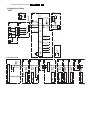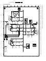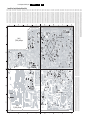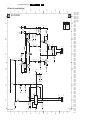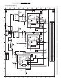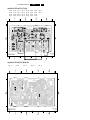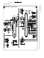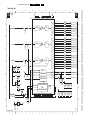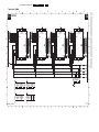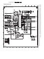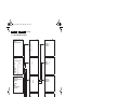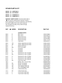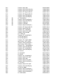
1
L05U_AA_312278515051.book Page 1 Friday, March 4, 2005 10:42 AM
Colour Television
Chassis
L05U
AA
FAMILY,
OR
MULTI BOARD
F_15050_000.eps
210205
Contents
Page
1. Technical Specifications, Connections, and Chassis
Overview
2
2. Safety Instructions, Warnings, and Notes
4
3. Directions for Use
6
4. Mechanical Instructions
7
5. Service Modes, Error Codes, and Fault Finding 10
6. Block Diagrams, Testpoint Overviews, and
Waveforms
Wiring Diagram
21
Block Diagram Supply and Deflection
22
Testpoint Overview Mono Carrier
23
Block Diagram Video
24
Testpoint Overview CRT Panel (Family Board) 25
Testpoint Overview HDMI Panel
25
Block Diagram Audio
24
Block Diagram Control & I2C Overview
27
Supply Lines Overview
28
7. Circuit Diagrams and PWB Layouts
Diagram
Mono Carrier: Power Supply
(A1) 29
Mono Carrier: Deflection
(A2) 30
Mono Carrier: Tuner IF
(A3) 31
Mono Carrier: Hercules
(A4) 32
Mono Carrier: Features & Connectivities
(A5) 33
Mono Carrier: Audio Amplifier
(A7) 34
Mono Carrier: Rear I/O Cinch
(A8) 35
Mono Carrier: Front Control
(A9) 36
Mono Carrier: AUX Power Supply
(A10) 37
CRT Panel (Family Board)
(B1) 44
CRT Panel: Eco Scavem (Family Board) (B2) 45
CRT Panel (Multi Board)
(B1) 48
CRT Panel: RGB Amplifier (Multi Board)
(B2) 49
CRT Panel: Rot. & SCAVEM (Multi Board) (B3) 50
Side AV + HP Panel (PV0-2)
(D) 52
Side AV + HP Panel (FL13)
(D) 54
Contents
8.
9.
PWB
38-43
38-43
38-43
38-43
38-43
38-43
38-43
38-43
38-43
46-47
46-47
51
51
51
53
55
10.
11.
Page
Top Control Panel (PV0)
(E) 56
Top Control Panel (PV2)
(E) 58
Top Control Panel (FL13)
(P) 59
Front Interface Panel (FL13)
(J) 61
Front Interface Panel (PV0-2)
(J) 61
HDMI Link Receiver
(M1) 64
HDMI + DMP
(M2) 65
Trident Panel: SVP
(T1) 67
Trident Panel: Source Select & uP
(T2) 68
Trident Panel: ADC
(T3) 69
Trident Panel: SDRAM
(T4) 70
Trident Panel: Deflection Controller
(T5) 71
Alignments
75
Circuit Descriptions, List of Abbreviations, and IC
Data Sheets
81
Abbreviation list
83
IC Data Sheets
84
Spare Parts List
85
Revision List
86
57
58
60
62
63
66
66
72-74
72-74
72-74
72-74
72-74
©
Copyright 2005 Philips Consumer Electronics B.V. Eindhoven, The Netherlands.
All rights reserved. No part of this publication may be reproduced, stored in a
retrieval system or transmitted, in any form or by any means, electronic,
mechanical, photocopying, or otherwise without the prior permission of Philips.
Published by BB 0563 TV Service
Printed in the Netherlands
Subject to modification
EN 3122 785 15051
L05U_AA_312278515051.book Page 2 Friday, March 4, 2005 10:42 AM
EN 2
1.
Technical Specifications, Connections, and Chassis Overview
L05U AA
1. Technical Specifications, Connections, and Chassis Overview
1.2
Index of this chapter:
1.1 Technical Specifications
1.2 Connections
1.3 Chassis Overview
Note: The following connector color abbreviations are used
(acc. to DIN/IEC 757): Bk= Black, Bu= Blue, Gn= Green, Gy=
Grey, Rd= Red, Wh= White, Ye= Yellow.
Notes:
• Described specifications are valid for the whole product
range.
• Figures below can deviate slightly from the actual situation,
due to different set executions.
1.1
Technical Specifications
1.1.1
Reception
Display type
Screen size
Tuning system
Color systems
Sound systems
Channel selections
IF picture carrier
Aerial input
A/V Connections
:
:
:
:
:
:
:
:
:
:
:
:
1.2.1
Top Control and Front / Side Connections
FRONT I/O
CRT-DV-SF
27”, 4:3
29”, 4:3
30”, 16:9
32”, 16:9
PLL
NTSC
BTSC
181, full cable
45.75 MHz
75 ohm, F-type
NTSC M (3.58 - 4.5)
LIGHT SENSOR IR RED
LED
(OPTIONAL)
TOP CONTROL
- VOL +
MENU
CH
SIDE I/O
Miscellaneous
S-VIDEO
: 2 x 10 W
Power supply:
- Mains voltage range
- Mains frequency
: 90 - 276 V_ac
: 50 / 60 Hz
Ambient conditions:
- Temperature range
- Maximum humidity
Power consumption:
- Normal operation
- Standby
VIDEO R AUDIO L
F_15050_005.eps
110205
Figure 1-1 Top control and Front / Side connections
: +5 to +45 °C
: 90% R.H.
: from 119 W
: to 133 W
: <1W
1.2.2
Hosiden: SVHS - In
1 - GND
2 - GND
3 -Y
4 -C
Ground
Ground
1 Vpp / 75 ohm
0.3 Vpp / 75 ohm
Audio / Video In
Ye - Video (CVBS)
Wh - Audio - L
Rd - Audio - R
Bk - Headphone
1 V_pp / 75 ohm
0.2 V_rms / 10 kohm
0.2 V_rms / 10 kohm
8 - 600 Ohm / 4 mW
H
H
j
j
jq
jq
jq
ot
Rear Connections
1
2
Audio output:
19
18
1.1.2
Connections
HDMI
75 Ohm
MONITOR
OUT
AV1
IN
AV2
IN
VIDEO
Y
L/Mono
V
V
Pb
L
L
Pr
R
R
AUDIO
ComPair
R
S-VIDEO
COMPONENT VIDEO INPUT
F_15050_006.eps
110205
Figure 1-2 Rear connections
L05U_AA_312278515051.book Page 3 Friday, March 4, 2005 10:42 AM
Technical Specifications, Connections, and Chassis Overview
Aerial In
- F-type
1.3
Coax, 75 ohm
L05U AA
1.
EN 3
Rd - Audio - R
0.5 V_rms / 10 kohm
jq
AV2 In (SVHS)
1 - Ground
2 - Ground
3 -Y
4 -C
GND
GND
1 V_pp / 75 ohm
0.3 V_pp / 75 ohm
H
H
jq
jq
D
Monitor Out
Ye - Video (CVBS)
Wh - Audio - L
Rd - Audio - R
1 V_pp / 75 ohm
0.5 V_rms / 1 kohm
0.5 V_rms / 1 kohm
kq
kq
kq
YUV In
Bu - U
Rd - V
Gn - Y
0.7 V_pp / 75 ohm
0.7 V_pp / 75 ohm
0.7 V_pp / 75 ohm
jq
jq
jq
AV1 In
Ye - Video (CVBS)
Wh - Audio - L
Rd - Audio - R
1 V_pp / 75 ohm
0.5 V_rms / 10 kohm
0.5 V_rms / 10 kohm
jq
jq
jq
AV2 In
Ye - Video (CVBS)
Wh - Audio - L
1 V_pp / 75 ohm
0.5 V_rms / 10 kohm
jq
jq
Chassis Overview
B1
CRT
B2
ECO
SCAVEM
B3
ROT &
SCAVEM (Only when Multi Board is used)
D
CRT PANEL
TOP CONTROL PANEL
FRONT INTERFACE PANEL
SIDE AV PANEL +
HEADPHONE
M
HDMI
PANEL
T
TRIDENT
PANEL
E/P
J
FAMILY,
OR
MULTI BOARD
MONO
CARRIER
POWER SUPPLY
A1
LINE DEFLECTION
A2
TUNER IF
A3
HERCULES
A4
FEATURES & CONNECTIVITIES
A5
CLASS D AUDIO AMPLIFIER
A6
AUDIO AMPLIFIER
A7
REAR I/O CINCH
A8
FRONT CONTROL
A9
DVD POWER SUPPLY
A10
F_15050_007.eps
040305
Figure 1-3 PWB location
L05U_AA_312278515051.book Page 4 Friday, March 4, 2005 10:42 AM
EN 4
2.
L05U AA
Safety Instructions, Warnings, and Notes
2. Safety Instructions, Warnings, and Notes
Index of this chapter:
2.1 Safety Instructions
2.2 Warnings
2.3 Notes
•
2.1
Safety Instructions
Safety regulations require that during a repair:
• Connect the set to the Mains (AC Power) via an isolation
transformer (> 800 VA).
• Replace safety components, indicated by the symbol h,
only by components identical to the original ones. Any
other component substitution (other than original type) may
increase risk of fire or electrical shock hazard.
Safety regulations require that after a repair, the set must be
returned in its original condition. Pay in particular attention to
the following points:
• Route the wire trees correctly and fix them with the
mounted cable clamps.
• Check the insulation of the Mains (AC Power) lead for
external damage.
• Check the strain relief of the Mains (AC Power) cord for
proper function.
• Check the electrical DC resistance between the Mains (AC
Power) plug and the secondary side (only for sets which
have a Mains (AC Power) isolated power supply):
1. Unplug the Mains (AC Power) cord and connect a wire
between the two pins of the Mains (AC Power) plug.
2. Set the Mains (AC Power) switch to the "on" position
(keep the Mains (AC Power) cord unplugged!).
3. Measure the resistance value between the pins of the
Mains (AC Power) plug and the metal shielding of the
tuner or the aerial connection on the set. The reading
should be between 4.5 Mohm and 12 Mohm.
4. Switch "off" the set, and remove the wire between the
two pins of the Mains (AC Power) plug.
• Check the cabinet for defects, to avoid touching of any
inner parts by the customer.
2.2
Warnings
•
•
•
•
All ICs and many other semiconductors are susceptible to
electrostatic discharges (ESD w). Careless handling
during repair can reduce life drastically. Make sure that,
during repair, you are connected with the same potential as
the mass of the set by a wristband with resistance. Keep
components and tools also at this same potential. Available
ESD protection equipment:
– Complete kit ESD3 (small tablemat, wristband,
connection box, extension cable and earth cable) 4822
310 10671.
– Wristband tester 4822 344 13999.
Be careful during measurements in the high voltage
section.
Never replace modules or other components while the unit
is switched "on".
When you align the set, use plastic rather than metal tools.
This will prevent any short circuits and the danger of a
circuit becoming unstable.
2.3
Notes
2.3.1
General
•
Measure the voltages and waveforms with regard to the
chassis (= tuner) ground (H), or hot ground (I), depending
on the tested area of circuitry. The voltages and waveforms
shown in the diagrams are indicative. Measure them in the
•
•
2.3.2
Schematic Notes
•
•
•
•
•
•
2.3.3
Service Default Mode (see chapter 5) with a colour bar
signal and stereo sound (L: 3 kHz, R: 1 kHz unless stated
otherwise) and picture carrier at 475.25 MHz for PAL, or
61.25 MHz for NTSC (channel 3).
Where necessary, measure the waveforms and voltages
with (D) and without (E) aerial signal. Measure the
voltages in the power supply section both in normal
operation (G) and in stand-by (F). These values are
indicated by means of the appropriate symbols.
The semiconductors indicated in the circuit diagram and in
the parts lists, are interchangeable per position with the
semiconductors in the unit, irrespective of the type
indication on these semiconductors.
Manufactured under license from Dolby Laboratories.
“Dolby”, “Pro Logic” and the “double-D symbol”, are
trademarks of Dolby Laboratories.
All resistor values are in ohms and the value multiplier is
often used to indicate the decimal point location (e.g. 2K2
indicates 2.2 kohm).
Resistor values with no multiplier may be indicated with
either an "E" or an "R" (e.g. 220E or 220R indicates 220
ohm).
All capacitor values are given in micro-farads (µ= x10-6),
nano-farads (n= x10-9), or pico-farads (p= x10-12).
Capacitor values may also use the value multiplier as the
decimal point indication (e.g. 2p2 indicates 2.2 pF).
An "asterisk" (*) indicates component usage varies. Refer
to the diversity tables for the correct values.
The correct component values are listed in the Spare Parts
List. Therefore, always check this list when there is any
doubt.
Rework on BGA (Ball Grid Array) ICs
General
Although (LF)BGA assembly yields are very high, there may
still be a requirement for component rework. By rework, we
mean the process of removing the component from the PWB
and replacing it with a new component. If an (LF)BGA is
removed from a PWB, the solder balls of the component are
deformed drastically so the removed (LF)BGA has to be
discarded.
Device Removal
As is the case with any component that, it is essential when
removing an (LF)BGA, the board, tracks, solder lands, or
surrounding components are not damaged. To remove an
(LF)BGA, the board must be uniformly heated to a temperature
close to the reflow soldering temperature. A uniform
temperature reduces the chance of warping the PWB.
To do this, we recommend that the board is heated until it is
certain that all the joints are molten. Then carefully pull the
component off the board with a vacuum nozzle. For the
appropriate temperature profiles, see the IC data sheet.
Area Preparation
When the component has been removed, the vacant IC area
must be cleaned before replacing the (LF)BGA.
Removing an IC often leaves varying amounts of solder on the
mounting lands. This excessive solder can be removed with
either a solder sucker or solder wick. The remaining flux can be
removed with a brush and cleaning agent.
After the board is properly cleaned and inspected, apply flux on
the solder lands and on the connection balls of the (LF)BGA.
Note: Do not apply solder paste, as this has shown to result in
problems during re-soldering.
L05U_AA_312278515051.book Page 5 Friday, March 4, 2005 10:42 AM
Safety Instructions, Warnings, and Notes
Device Replacement
The last step in the repair process is to solder the new
component on the board. Ideally, the (LF)BGA should be
aligned under a microscope or magnifying glass. If this is not
possible, try to align the (LF)BGA with any board markers.
To reflow the solder, apply a temperature profile according to
the IC data sheet. So as not to damage neighbouring
components, it may be necessary to reduce some
temperatures and times.
•
Lead Free Solder
Philips CE is going to produce lead-free sets (PBF) from
1.1.2005 onwards.
2.3.5
P
Figure 2-1 Lead-free logo
This sign normally has a diameter of 6 mm, but if there is less
space on a board also 3 mm is possible.
Regardless of this logo (is not always present), one must treat
all sets from this date onwards according to the following rules.
Due to lead-free technology some rules have to be respected
by the workshop during a repair:
• Use only lead-free soldering tin Philips SAC305 with order
code 0622 149 00106. If lead-free solder paste is required,
please contact the manufacturer of your soldering
equipment. In general, use of solder paste within
workshops should be avoided because paste is not easy to
store and to handle.
• Use only adequate solder tools applicable for lead-free
soldering tin. The solder tool must be able
– To reach at least a solder-tip temperature of 400°C.
– To stabilise the adjusted temperature at the solder-tip.
– To exchange solder-tips for different applications.
• Adjust your solder tool so that a temperature around 360°C
- 380°C is reached and stabilised at the solder joint.
Heating time of the solder-joint should not exceed ~ 4 sec.
Avoid temperatures above 400°C, otherwise wear-out of
tips will rise drastically and flux-fluid will be destroyed. To
avoid wear-out of tips, switch “off” unused equipment or
reduce heat.
• Mix of lead-free soldering tin/parts with leaded soldering
tin/parts is possible but PHILIPS recommends strongly to
avoid mixed regimes. If not to avoid, clean carefully the
solder-joint from old tin and re-solder with new tin.
• Use only original spare-parts listed in the Service-Manuals.
Not listed standard material (commodities) has to be
purchased at external companies.
• Special information for lead-free BGA ICs: these ICs will be
delivered in so-called "dry-packaging" to protect the IC
against moisture. This packaging may only be opened
short before it is used (soldered). Otherwise the body of the
IC gets "wet" inside and during the heating time the
structure of the IC will be destroyed due to high (steam)pressure inside the body. If the packaging was opened
before usage, the IC has to be heated up for some hours
(around 90°C) for drying (think of ESD-protection!).
EN 5
Do not re-use BGAs at all!
For sets produced before 1.1.2005, containing leaded
soldering tin and components, all needed spare parts will
be available till the end of the service period. For the repair
of such sets nothing changes.
Practical Service Precautions
•
b
2.
In case of doubt whether the board is lead-free or not (or with
mixed technologies), you can use the following method:
• Always use the highest temperature to solder, when using
SAC305 (see also instructions below).
• De-solder thoroughly (clean solder joints to avoid mix of
two alloys).
Caution: For BGA-ICs, you must use the correct temperatureprofile, which is coupled to the 12NC. For an overview of these
profiles, visit the website www.atyourservice.ce.philips.com
(needs subscription, but is not available for all regions)
You will find this and more technical information within the
"Magazine", chapter "Workshop information".
For additional questions please contact your local repair help
desk.
More Information
For more information on how to handle BGA devices, visit this
URL: www.atyourservice.ce.philips.com (needs subscription,
not available for all regions). After login, select “Magazine”,
then go to “Workshop Information”. Here you will find
Information on how to deal with BGA-ICs.
2.3.4
L05U AA
•
It makes sense to avoid exposure to electrical shock.
While some sources are expected to have a possible
dangerous impact, others of quite high potential are of
limited current and are sometimes held in less regard.
Always respect voltages. While some may not be
dangerous in themselves, they can cause unexpected
reactions that are best avoided. Before reaching into a
powered TV set, it is best to test the high voltage insulation.
It is easy to do, and is a good service precaution.
L05U_AA_312278515051.book Page 6 Friday, March 4, 2005 10:42 AM
EN 6
3.
L05U AA
Directions for Use
3. Directions for Use
You can download this information from the following websites:
http://www.philips.com/support
http://www.p4c.philips.com
L05U_AA_312278515051.book Page 7 Friday, March 4, 2005 10:42 AM
Mechanical Instructions
L05U AA
4.
EN 7
4. Mechanical Instructions
Index of this chapter:
4.1 Set Disassembly
4.2 Service Position
4.3 Assy/Panel Removal
4.4 Set Re-assembly
Note: Figures below can deviate slightly from the actual
situation, due to different set executions.
4.1
Set Disassembly
2
Warning: Be sure to disconnect the AC power from the set
before opening it.
4.1.1
Rear Cover
1. Remove all screws. If you do not remove them, you cannot
access the clips.
2. Tilt the set a little forward, so that you can release the two
clickfit clamps that are located at the bottomplate of the set.
3. Four openings (1) can be found at the top. The openings
are very small (2).
Note: Some sets only have the two inner openings.
4. Underneath every opening there is a clip. Push this clip
down with a very thin piece of metal (3), until you hear a
click.
Caution: do not use a screwdriver, this will damage the
cabinet.
5. When all four clips are pushed down, the back cover can
be removed.
E_13950_012 .eps
050404
Figure 4-2 Opening
3
1
E_13950_013.eps
050404
Figure 4-3 Pushing clips down
4.2
E_13950_011 .eps
050404
Figure 4-1 Rear cover (for FL13 styling)
Service Position
Before placing the Mono Carrier in its service position, remove
the Front Interface assy/panel (see paragraph “Front Interface
Assy/Panel”) and the Side AV assy/panel (see paragraph “Side
AV Assy/Panel”).
L05U_AA_312278515051.book Page 8 Friday, March 4, 2005 10:42 AM
EN 8
4.
L05U AA
Mechanical Instructions
4.3
Assy/Panel Removal
4.3.1
Front Interface Assy/Panel
1
1
1
1
2
F_15050_008.eps
110205
2
Figure 4-4 Mono Carrier
F_15050_010.eps
110205
Figure 4-6 Front interface assy/panel removal
1. Remove the two fixation screws.
2. Remove the complete module from the bottom plate, by
pulling the two fixation clamps upward [1], while sliding the
module away from the CRT [2].
3. Release the two fixation clamps at the side of the bracket,
and lift the panel out of the bracket (it hinges at one side).
4.3.2
Side AV Assy/Panel
1. Remove the fixation screw, and remove the complete Side
AV assembly.
2. Release the two fixation clamps, and lift the panel out of the
bracket.
3
4.3.3
To remove the HDMI Interface panel from the Mono Carrier,
unscrew the fixation screw at the back of the assy.
F_15050_009.eps
110205
Figure 4-5 Service position Mono Carrier
1. Disconnect the degaussing coil.
2. Release the two fixation clamps [1] (at the mid left and mid
right side of the bracket), and remove the bracket from the
bottom tray, by pulling it backwards [2].
3. Move the panel bracket somewhat to the left and flip it 90
degrees [3], with the components towards the CRT.
4. Turn the panel bracket with the rear I/O toward the CRT.
HDMI Interface Panel
4.3.4
Trident Panel
1. Remove all cables.
2. Pull the panel upwards out of the connectors.
4.3.5
Top Control Assy/Panel
4
4
3
2
2
3
1
1
F_15050_012.eps
110205
Figure 4-7 Top Control assy/panel removal
1. Remove the two fixation screws at the bottom [1] and the
two fixation screws at the front of the assy [2].
2. Release the two fixation clamps [3] to lift out the assy.
3. Release the two fixation clamps [4] to lift the panel out of
the assy.
L05U_AA_312278515051.book Page 9 Friday, March 4, 2005 10:42 AM
Mechanical Instructions
4.4
Set Re-assembly
To re-assemble the whole set, do all processes in reverse
order.
Note: before you mount the rear cover, perform the following
checks:
• Check whether the AC power cord is mounted correctly in
its guiding brackets.
• Check whether all cables are replaced in their original
position
L05U AA
4.
EN 9
L05U_AA_312278515051.book Page 10 Friday, March 4, 2005 10:42 AM
EN 10
5.
L05U AA
Service Modes, Error Codes, and Fault Finding
5. Service Modes, Error Codes, and Fault Finding
•
Index of this chapter:
5.1 Test Points
5.2 Service Modes
5.3 Problems and Solving Tips Related to CSM
5.4 ComPair
5.5 Error Codes
5.6 The Blinking LED Procedure
5.7 Protections
5.8 Fault Finding and Repair Tips
5.1
Test Points
This chassis is equipped with test points in the service printing.
In the schematics test points are identified with a rectangle box
around Fxxx or Ixxx. These test points are specifically
mentioned in the “Test Point Overview” as “half moons” with a
dot in the center.
Table 5-1 Test point overview
Test point
Circuit
Diagr.
F508, F535, F536, F537, F552, F561, F563, F573, F664, Power supply
I513, I518, I519, I524, I531, I533, I546
A1
F401, F412, F413, F414, F418, F452, F453, F455, F456, Line & Frame
F458, F459, F460, F461, I408, I416, I417, I420, I462,
Deflection
I468
A2
F003, F004, I001, I002
Tuner IF
A3
F201, F203, F205, F206
Hercules
A4
F240, F241, F242
Features &
Connectivities
A5
F952, F955, I951, I952
Audio Amplifier A7
F692
Front Control
A9
F331, F332, F333, F338, F339, F341, F351, F353, F354 CRT Panel
B1
F361, F362, F381, F382
B2
ECO Scavem
Perform measurements under the following conditions:
• Television set in Service Default Alignment Mode.
• Video input: Color bar signal.
• Audio input: 3 kHz left channel, 1 kHz right channel.
5.2
All service-unfriendly modes (if present) are disabled. The
service unfriendly modes are:
– Timer / Sleep timer.
– Child / parental lock.
– Blue mute.
– Hotel / hospital mode.
– Auto shut off (when no “IDENT” video signal is
received for 15 minutes).
– Skipping of non-favorite presets / channels.
– Auto-storage of personal presets.
– Auto user menu time-out.
– Auto Volume Leveling (AVL).
How to enter
To enter SDM, use one of the following methods:
• Press the following key sequence on the remote control
transmitter: “062596” directly followed by the MENU button
(do not allow the display to time out between entries while
keying the sequence).
• Short the jumper wire 9252 with a cold ground on the family
board (for example the tuner casing) and apply AC power.
Then press the power button (remove the short after startup).
Caution: Entering SDM by shorting wire 9252 with ground
will override the +8V-protection. Do this only for a short
period. When doing this, the service-technician must know
exactly what he is doing, as it could damage the television
set.
• Or via ComPair.
After entering SDM, the following screen is visible, with SDM in
the upper right corner of the screen to indicate that the
television is in Service Default Alignment Mode.
00028 L05US1 1.1 PUS1 0.7 SDM
ERR 0 0 0 0 0
OP 000 057 140 032 120 128 000
Service Modes
Service Default mode (SDM) and Service Alignment Mode
(SAM) offers several features for the service technician, while
the Customer Service Mode (CSM) is used for communication
between the call center and the customer.
This chassis also offers the option of using ComPair, a
hardware interface between a computer and the TV chassis. It
offers the abilities of structured troubleshooting, error code
reading, and software version readout for all chassis.
Minimum requirements for ComPair: a Pentium processor, a
Windows OS, and a CD-ROM drive (see also paragraph
"ComPair").
F_15050_013.eps
110205
Figure 5-1 SDM menu
5.2.1
Service Default Mode (SDM)
Purpose
• To create a predefined setting for measurements to be
made.
• To override software protections.
• To start the blinking LED procedure.
Specifications
• Tuning frequency: 61.25 MHz (channel 3).
• Color system: NTSC M.
• All picture settings at 50% (brightness, color contrast, hue).
• Bass, treble and balance at 50 %; volume at 25 %.
L05U_AA_312278515051.book Page 11 Friday, March 4, 2005 10:42 AM
Service Modes, Error Codes, and Fault Finding
How to navigate
Use one of the following methods:
• When you press the MENU button on the remote control,
the set will switch on the normal user menu in the SDM
mode.
• On the TV, press and hold the VOLUME DOWN and press
the CHANNEL DOWN for a few seconds, to switch from
SDM to SAM and reverse.
How to exit
Switch the set to STANDBY by pressing the POWER button on
the remote control transmitter or the television set.
If you turn the television set off by removing the AC power (i.e.,
unplugging the television) without using the POWER button,
the television set will remain in SDM when AC power is reapplied, and the error buffer is not cleared.
5.2.2
Service Alignment Mode (SAM)
Purpose
• To change option settings.
• To display / clear the error code buffer.
• To perform alignments.
Specifications
• Operation hours counter (maximum five digits displayed).
• Software version, Error codes, and Option settings display.
• Error buffer clearing.
• Option settings.
• AKB switching.
• Software alignments (Tuner, White Tone, Geometry &
Audio).
• NVM Editor.
• ComPair Mode switching.
How to enter
To enter SAM, use one of the following methods:
• Press the following key sequence on the remote control
transmitter: “062596" directly followed by the OSD/
STATUS button (do not allow the display to time out
between entries while keying the sequence).
• Or via ComPair.
After entering SAM, the following screen is visible, with SAM in
the upper right corner of the screen to indicate that the
television is in Service Alignment Mode.
00028 L05US1 1.1 PUS1 0.7
ERR 0 0 0 0 0
SAM
OP 000 057 140 032 120 128 000
. Clear
. Options
. AKB
. Tuner
. White Tone
. Geometry
. Audio
. NVM Editor
. ComPair
Clear ?
On
on
F_15050_014.eps
110205
Figure 5-2 SAM menu
L05U AA
5.
EN 11
Menu explanation
1. LLLLL. This represents the run timer. The run timer counts
normal operation hours, but does not count standby hours.
2. AAABCD-x.y. This is the software identification of the
main microprocessor:
– A= the project name (= L05).
– B= the region: E= Europe, A= Asia Pacific, U= NAFTA,
L= LATAM.
– C= the software diversity:
• Europe: T= 1 page TXT, F= Full TXT, V= Voice
control.
• LATAM and NAFTA: N= Stereo non-dBx, S=
Stereo dBx.
• Asian Pacific: T= TXT, N= non-TXT, C= NTSC.
• ALL regions: M= mono, D= DVD, Q= Mk2.
– D= the language cluster number.
– x= the main software version number (updated with a
major change that is incompatible with previous
versions).
– y= the sub software version number (updated with a
minor change that is compatible with previous
versions).
3. EFFG-x.y. This is the software identification of the Trident
microprocessor.
– P= indication of the Trident processor.
– FF= the region: US=Nafta.
– G= the language cluster number.
– x= the main software version number (updated with a
major change that is incompatible with previous
versions).
– y= the sub software version number (updated with a
minor change that is compatible with previous
versions).
4. SAM. Indication of the Service Alignment Mode.
5. Error Buffer. Shows all errors detected since the last time
the buffer was erased. Five errors possible.
6. Option Bytes. Used to set the option bytes. See “Options”
in the Alignments section for a detailed description. Seven
codes are possible.
7. Clear. Erases the contents of the error buffer. Select the
CLEAR menu item and press the MENU RIGHT key. The
content of the error buffer is cleared.
8. Options. Used to set the option bits. See “Options” in the
Alignments section for a detailed description.
9. AKB. Used to disable (Off) or enable (On) the “black
current loop” (AKB= Auto Kine Bias).
10. Tuner. Used to align the tuner. See “Tuner” in the
Alignments section for a detailed description.
11. White Tone. Used to align the white tone. See “White
Tone” in the Alignments section for a detailed description.
12. Geometry. Used to align the geometry settings of the
television. See “Geometry” in the Alignments section for a
detailed description.
13. Audio. No audio alignment is necessary for this television
set.
14. NVM Editor. Can be used to change the NVM data in the
television set. See table “NVM data” further on.
15. ComPair. Can be used to switch on the television to In
System Programming (ISP) mode, for software uploading
via ComPair. Caution: When this mode is selected without
ComPair connected, the TV will be blocked. Remove the
AC power to reset the TV.
How to navigate
• In SAM, select menu items with the MENU UP/DOWN keys
on the remote control transmitter. The selected item will be
highlighted. When not all menu items fit on the screen, use
the MENU UP/DOWN keys to display the next / previous
menu items.
• With the MENU LEFT/RIGHT keys, it is possible to:
– Activate the selected menu item.
– Change the value of the selected menu item.
– Activate the selected submenu.
• In SAM, when you press the MENU button twice, the set
will switch to the normal user menus (with the SAM mode
L05U_AA_312278515051.book Page 12 Friday, March 4, 2005 10:42 AM
EN 12
•
5.
L05U AA
Service Modes, Error Codes, and Fault Finding
6. Indicates the television is receiving an "IDENT" signal on
the selected source. If no "IDENT" signal is detected, the
display will read "NOT TUNED"
7. Displays the detected Color system (e.g. PAL/NTSC).
8. Displays the detected Audio (e.g. stereo/mono).
9. Displays the picture setting information.
10. Displays the sound setting information.
still active in the background). To return to the SAM menu
press the MENU or STATUS/EXIT button.
When you press the MENU key in while in a submenu, you
will return to the previous menu.
How to store SAM settings
To store the settings changed in SAM mode, leave the top level
SAM menu by using the POWER button on the remote control
transmitter or the television set.
How to exit
Switch the set to STANDBY by pressing the POWER button on
the remote control transmitter or the television set.
If you turn the television set “off” by removing the AC power
(i.e., unplugging the television) without using the POWER
button, the television set will remain in SAM when AC power is
re-applied, and the error buffer is not cleared.
5.2.3
Customer Service Mode (CSM)
Purpose
The Customer Service Mode shows error codes and
information on the TV’s operation settings. The call center can
instruct the customer (by telephone) to enter CSM in order to
identify the status of the set. This helps the call center to
diagnose problems and failures in the TV set before making a
service call.
The CSM is a read-only mode; therefore, modifications are not
possible in this mode.
How to enter
To enter CSM, press the following key sequence on the remote
control transmitter: “123654” (do not allow the display to time
out between entries while keying the sequence).
Upon entering the Customer Service Mode, the following
screen will appear:
1 00028 L05US1 1.1 PUS1 0.7 CSM
2 CODES 0 0 0 0 0
3 OP 000 057 140 032 120 128 000
4 nnXXnnnn/nnX
5 P3C-1
6 NOT TUNED
7 NTSC
8 STEREO
9 CO 50 CL 50 BR 50 HU 0
0 AVL Off BS 50
How to exit
To exit CSM, use one of the following methods:
• Press the MENU, STATUS/EXIT, or POWER button on the
remote control transmitter.
• Press the POWER button on the television set.
5.3
Problems and Solving Tips Related to CSM
5.3.1
Picture Problems
Note: The problems described below are all related to the TV
settings. The procedures used to change the value (or status)
of the different settings are described.
Picture too dark or too bright
If:
• The picture improves when you have press the AUTO
PICTURE button on the remote control transmitter, or
• The picture improves when you enter the Customer
Service Mode,
Then:
1. Press the AUTO PICTURE button on the remote control
transmitter repeatedly (if necessary) to choose
PERSONAL picture mode.
2. Press the MENU button on the remote control transmitter.
This brings up the normal user menu.
3. In the normal user menu, use the MENU UP/DOWN keys
to highlight the PICTURE sub menu.
4. Press the MENU LEFT/RIGHT keys to enter the PICTURE
sub menu.
5. Use the MENU UP/DOWN keys (if necessary) to select
BRIGHTNESS.
6. Press the MENU LEFT/RIGHT keys to increase or
decrease the BRIGHTNESS value.
7. Use the MENU UP/DOWN keys to select PICTURE.
8. Press the MENU LEFT/RIGHT keys to increase or
decrease the PICTURE value.
9. Press the MENU button on the remote control transmitter
twice to exit the user menu.
10. The new PERSONAL preference values are automatically
stored.
White line around picture elements and text
F_15050_015.eps
140205
Figure 5-3 CSM menu
Menu explanation
1. Indication of the decimal value of the operation hours
counter, Software identification of the main and Trident
microprocessor (see "Service Default or Alignment Mode"
for an explanation), and the service mode (CSM=
Customer Service Mode).
2. Displays the last five errors detected in the error code
buffer.
3. Displays the option bytes.
4. Displays the type number version of the set.
5. Reserved item for P3C call centers.
If:
The picture improves after you have pressed the AUTO
PICTURE button on the remote control transmitter,
Then:
1. Press the AUTO PICTURE button on the remote control
transmitter repeatedly (if necessary) to choose
PERSONAL picture mode.
2. Press the MENU button on the remote control transmitter.
This brings up the normal user menu.
3. In the normal user menu, use the MENU UP/DOWN keys
to highlight the PICTURE sub menu.
4. Press the MENU LEFT/RIGHT keys to enter the PICTURE
sub menu.
5. Use the MENU UP/DOWN keys to select SHARPNESS.
6. Press the MENU LEFT key to decrease the SHARPNESS
value.
L05U_AA_312278515051.book Page 13 Friday, March 4, 2005 10:42 AM
Service Modes, Error Codes, and Fault Finding
•
7. Press the MENU button on the remote control transmitter
twice to exit the user menu.
8. The new PERSONAL preference value is automatically
stored.
•
Snowy picture
Check CSM line 6. If this line reads “Not Tuned”, check the
following:
• Antenna not connected. Connect the antenna.
• No antenna signal or bad antenna signal. Connect a proper
antenna signal.
• The tuner is faulty (in this case line 2, the Error Buffer line,
will contain error number 10). Check the tuner and replace/
repair the tuner if necessary.
Black and white picture
If:
• The picture improves after you have pressed the AUTO
PICTURE button on the remote control transmitter,
Then:
1. Press the AUTO PICTURE button on the remote control
transmitter repeatedly (if necessary) to choose
PERSONAL picture mode.
2. Press the MENU button on the remote control transmitter.
This brings up the normal user menu.
3. In the normal user menu, use the MENU UP/DOWN keys
to highlight the PICTURE sub menu.
4. Press the MENU LEFT/RIGHT keys to enter the PICTURE
sub menu.
5. Use the MENU UP/DOWN keys to select COLOR.
6. Press the MENU RIGHT key to increase the COLOR value.
7. Press the MENU button on the remote control transmitter
twice to exit the user menu.
8. The new PERSONAL preference value is automatically
stored.
Menu text not sharp enough
If:
• The picture improves after you have pressed the AUTO
PICTURE button on the remote control transmitter,
Then:
1. Press the AUTO PICTURE button on the remote control
transmitter repeatedly (if necessary) to choose
PERSONAL picture mode.
2. Press the MENU button on the remote control transmitter.
This brings up the normal user menu.
3. In the normal user menu, use the MENU UP/DOWN keys
to highlight the PICTURE sub menu.
4. Press the MENU LEFT/RIGHT keys to enter the PICTURE
sub menu.
5. Use the MENU UP/DOWN keys to select PICTURE.
6. Press the MENU LEFT key to decrease the PICTURE
value.
7. Press the MENU button on the remote control transmitter
twice to exit the user menu.
8. The new PERSONAL preference value is automatically
stored.
5.4
ComPair
5.4.1
Introduction
ComPair (Computer Aided Repair) is a service tool for Philips
Consumer Electronics products. ComPair is a further
development on the European DST (service remote control),
which allows faster and more accurate diagnostics. ComPair
has three big advantages:
•
5.4.2
L05U AA
5.
EN 13
ComPair helps you to quickly get an understanding on how
to repair the chassis in a short time by guiding you
systematically through the repair procedures.
ComPair allows very detailed diagnostics (on I2C level)
and is therefore capable of accurately indicating problem
areas. You do not have to know anything about I2C
commands yourself because ComPair takes care of this.
ComPair speeds up the repair time since it can
automatically communicate with the chassis (when the
microprocessor is working) and all repair information is
directly available. When ComPair is installed together with
the Force/SearchMan electronic manual of the defective
chassis, schematics and PWBs are only a mouse click
away.
Specifications
ComPair consists of a Windows based fault finding program
and an interface box between PC and the (defective) product.
The ComPair interface box is connected to the PC via a serial
(or RS232) cable.
For this chassis, the ComPair interface box and the TV
communicate via a bi-directional service cable via the service
connector(s).
The ComPair fault finding program is able to determine the
problem of the defective television. ComPair can gather
diagnostic information in two ways:
• Automatic (by communication with the television): ComPair
can automatically read out the contents of the entire error
buffer. Diagnosis is done on I2C/UART level. ComPair can
access the I2C/UART bus of the television. ComPair can
send and receive I2C/UART commands to the micro
controller of the television. In this way, it is possible for
ComPair to communicate (read and write) to devices on
the I2C/UART buses of the TV-set.
• Manually (by asking questions to you): Automatic
diagnosis is only possible if the micro controller of the
television is working correctly and only to a certain extend.
When this is not the case, ComPair will guide you through
the fault finding tree by asking you questions (e.g. Does the
screen give a picture? Click on the correct answer: YES /
NO) and showing you examples (e.g. Measure test-point I7
and click on the correct oscillogram you see on the
oscilloscope). You can answer by clicking on a link (e.g.
text or a waveform picture) that will bring you to the next
step in the fault finding process.
By a combination of automatic diagnostics and an interactive
question / answer procedure, ComPair will enable you to find
most problems in a fast and effective way.
Beside fault finding, ComPair provides some additional
features like:
• Up- or downloading of pre-sets.
• Managing of pre-set lists.
• Emulation of the (European) Dealer Service Tool (DST).
• If both ComPair and Force/SearchMan (Electronic Service
Manual) are installed, all the schematics and the PWBs of
the set are available by clicking on the appropriate
hyperlink.
Example: Measure the DC-voltage on capacitor C2568
(Schematic/Panel) at the Mono-carrier.
– Click on the “Panel” hyperlink to automatically show
the PWB with a highlighted capacitor C2568.
– Click on the “Schematic” hyperlink to automatically
show the position of the highlighted capacitor.
L05U_AA_312278515051.book Page 14 Friday, March 4, 2005 10:42 AM
EN 14
5.4.3
5.
Service Modes, Error Codes, and Fault Finding
L05U AA
5.5.2
How To Connect
This is described in the chassis fault finding database in
ComPair.
TO
UART SERVICE
CONNECTOR
PC
TO
I2C SERVICE
CONNECTOR
VCR
Power
9V DC
I2C
E_06532_021.eps
180804
Figure 5-4 ComPair interface connection
5.4.4
How To Order
ComPair order codes (EU/AP/LATAM):
• Starter kit ComPair32/SearchMan32 software and
ComPair interface (excl. transformer): 3122 785 90450.
• ComPair interface (excl. transformer): 4822 727 21631.
• Starter kit ComPair32 software (registration version): 3122
785 60040.
• Starter kit SearchMan32 software: 3122 785 60050.
• ComPair32 CD (update): 3122 785 60070 (year 2002),
3122 785 60110 (year 2003 onwards).
• SearchMan32 CD (update): 3122 785 60080 (year 2002),
3122 785 60120 (year 2003), 3122 785 60130 (year 2004).
• ComPair firmware upgrade IC: 3122 785 90510.
• Transformer (non-UK): 4822 727 21632.
• Transformer UK: 4822 727 21633.
• ComPair interface cable: 3122 785 90004.
• ComPair interface extension cable: 3139 131 03791.
• ComPair UART interface cable: 3122 785 90630
ComPair order codes (US):
• ComPair Software: ST4191.
• ComPair Interface Box: 4822 727 21631.
• AC Adapter: T405-ND.
• ComPair Quick Start Guide: ST4190.
• ComPair interface extension cable: 3139 131 03791.
• ComPair UART interface cable: 3122 785 90630
Note: If you encounter any problems, contact your local
support desk.
5.5
Error Codes
The error code buffer contains all errors detected since the last
time the buffer was erased. The buffer is written from left to
right. When an error occurs that is not yet in the error code
buffer, it is displayed at the left side and all other errors shift one
position to the right.
5.5.1
How To Read The Error Buffer
You can read the error buffer in 3 ways:
• On screen via the SAM (if you have a picture). Examples:
– ERROR: 0 0 0 0 0 : No errors detected
– ERROR: 6 0 0 0 0 : Error code 6 is the last and only
detected error
– ERROR: 9 6 0 0 0 : Error code 6 was detected first and
error code 9 is the last detected (newest) error
• Via the blinking LED procedure (when you have no
picture). See “The Blinking LED Procedure”.
• Via ComPair.
How To Clear The Error Buffer
The error code buffer is cleared in the following cases:
• By using the CLEAR command in the SAM menu:
– To enter SAM, press the following key sequence on the
remote control transmitter: “062596” directly followed
by the OSD/STATUS button (do not allow the display
to time out between entries while keying the
sequence).
– Make sure the menu item CLEAR is highlighted. Use
the MENU UP/DOWN buttons, if necessary.
– Press the MENU RIGHT button to clear the error
buffer. The text on the right side of the “CLEAR” line will
change from “CLEAR?” to “CLEARED”
• If the contents of the error buffer have not changed for 50
hours, the error buffer resets automatically.
Note: If you exit SAM by disconnecting the AC power from the
television set, the error buffer is not reset.
L05U_AA_312278515051.book Page 15 Friday, March 4, 2005 10:42 AM
Service Modes, Error Codes, and Fault Finding
5.5.3
L05U AA
5.
EN 15
If possible, check the entire contents of the error buffer. In
some situations, an error code is only the result of another error
and not the actual cause of the problem (for example, a fault in
the protection detection circuitry can also lead to a protection).
Error Codes
In case of non-intermittent faults, write down the errors present
in the error buffer and clear the error buffer before you begin
the repair. This ensures that old error codes are no longer
present.
Table 5-2 Error code overview
5.6
Error
Device
Error description
0
Not applicable
No Error
Check item
Diagram
1
Not applicable
2
Not applicable
X-Ray/Over-voltage protection (US only)
2411, 2412, 2413, 6404, 6411, 6412
A2
High beam (BCI) protection
3412, 7405
3
Not applicable
A2
Vertical guard protection
3466, 7451
A2
4
Not applicable
-
-
-
5
Not applicable
+5v protection
7604, 7605
A5
6
I2C bus
General I2C error
7200, 3207, 3214
A4
7
Not applicable
-
-
-
8
Not applicable
-
-
-
9
24C16
I2C error while communicating with the EEPROM
7601, 3604, 3605
A5
10
Tuner
I2C error while communicating with the PLL tuner
1000, 5001
A3
11
TDA6107/A
Black current loop instability protection
7330, 3351, CRT
B1
12
Not applicable
-
-
-
13
Not applicable
-
-
-
14
Not applicable
-
-
-
15
Not applicable
-
-
-
16
Not applicable
-
-
-
17
Not applicable
-
-
-
18
Not applicable
-
-
-
19
TDA1200x
I2C error while communicating with sound decoder in Hercules IC
7200
A4
20
TDA1200x
I2C error while communicating with video cosmic in Hercules IC
7200
A4
21
DPTVSVP
I2C error while communicating with the 3D Processor
7201, 3223, 3224
T1
22
TDA9332
I2C error while communicating with the HOP
7221, 3244, 3629, 7226, 7227
T5
23
SAA5565
I2C error while communicating with the Painter uProcessor
7206, 3254, 3256
T2
24
AD9883
I2C error while communicating with the ADC
7210, 3268, 3270
T3
25
Not applicable
No communication possible with Trident module
-
T
26
SII9993
I2C error while communicating with the HDMI receiver
7002, 3016, 3019
M1
The Blinking LED Procedure
•
•
Using this procedure, you can make the contents of the error
buffer visible via the front LED. This is especially useful when
there is no picture.
When the SDM is entered, the front LED will blink the contents
of the error-buffer:
• When all the error-codes are displayed, the sequence
finishes with a LED blink of 1.5 seconds,
• The sequence starts again.
Example of error buffer: 12 9 6 0 0
After entering SDM, the following occurs:
• 1 long blink of 5 seconds to start the sequence,
• 12 short blinks followed by a pause of 1.5 seconds,
• 9 short blinks followed by a pause of 1.5 seconds,
• 6 short blinks followed by a pause of 1.5 seconds,
• 1 long blink of 1.5 seconds to finish the sequence,
• The sequence starts again at 12 short blinks.
5.7
Protections
If a fault situation is detected, an error code will be generated;
and, if necessary, the television set will go into protection
mode. Blinking of the red LED at a frequency of 3 Hz indicates
the protection mode. In some error cases, the microprocessor
does not put the set in protection mode. The error codes of the
error buffer and the blinking LED procedure can be read via the
Service Default Menu (SDM), or via ComPair.
To get a quick diagnosis the chassis has three service modes
implemented:
• The Customer Service Mode (CSM).
The Service Default Mode (SDM).
The Service Alignment Mode (SAM).
For a detailed mode description, see the relevant sections.
5.8
Fault Finding and Repair Tips
Notes:
• It is assumed that the components are mounted correctly
with correct values and no bad solder joints.
• Before any fault finding actions, check if the correct options
are set.
5.8.1
NVM Editor
In some cases, it can be handy if one directly can change the
NVM contents. This can be done with the “NVM Editor” in SAM
mode. In the next table, the default NVM values are given.
L05U_AA_312278515051.book Page 16 Friday, March 4, 2005 10:42 AM
EN 16
5.
Service Modes, Error Codes, and Fault Finding
L05U AA
30MW5405
32PW8422
29PT8422
30PW8420
27PT8420
Item
Default values (hex)
27MT5405
Address (dec)
Table 5-3 NVM default values for NAFTA-region
EW (EW Width)
19
21
21
30
21
30
PW (EW Parabola Width)
20
18
18
14
18
14
30
14
HS (Horizontal Shift)
21
27
27
20
27
20
20
HP (Horizontal Parallelogram)
22
07
07
07
07
07
07
HB (Horizontal Bow)
23
07
07
07
07
07
07
UCP (EW Upper Corner Parabola)
24
1E
1E
1E
1E
1E
1E
LCP (EW Lower Corner Parabola)
25
21
21
19
21
19
19
TC (EW Trapezium)
26
1E
1E
1A
1E
1A
1A
VS (Vertical Slope)
27
32
32
30
32
30
30
VA (Vertical Amplitude)
28
18
18
1C
18
1C
1C
SC (S-Correction)
29
1E
1E
14
1E
14
14
VSH (Vertical Shift)
30
1A
1A
1A
1A
1A
1A
VX (Vertical Zoom)
31
19
19
19
19
19
19
VSL (Vertical Scroll)
32
20
20
20
20
20
20
EHTC (Vertical Linearity)
33
20
20
20
20
20
20
BLOR (Black Level Offset - Red)
34
07
07
08
07
08
08
BLOG (Black Level Offset - Green)
35
07
07
08
07
08
08
AGC (AGC Takeover)
36
1E
1E
1E
1E
1E
1E
OIF (IF-PLL Offset)
37
26
26
26
26
26
26
Vertival Wait
38
0F
0F
0F
0F
0F
0F
H60 and V60
39
09
09
09
09
09
09
60 Hz Vertical Amplitude
42
30
30
30
30
30
30
YD & CL
43
06
06
06
06
06
06
RGB amplitude for full teletext mode
46
00
00
00
00
00
00
NVM_TABLE_VERSION
60
10
10
10
10
10
10
OPTION_TABLE_VERSION
61
01
01
01
01
01
01
CVI_BLOR
62
03
03
08
03
08
08
CVI_BLOG
63
08
08
08
08
08
08
TXT Brightness
64
17
17
17
17
17
17
V60 offset (60Hz Vertical Amplitude)
66
FE
FE
FE
FE
FE
FE
FOAB, CHSE
139
03
03
03
03
03
03
NVM_SOC_SMD
142
10
10
10
10
10
10
NVM_FMWS
149
03
03
03
03
03
03
NVM_ASD_SC1_THR
150
10
10
10
10
10
10
NVM_CRYSTALALIGN
208
3F
3F
3F
3F
3F
3F
Last Brightness (VID PP others)
264
30
30
30
30
30
30
Last Color (VID PP others)
265
28
28
28
28
28
28
Last Contrast (VID PP others)
266
55
55
55
55
55
55
Last Sharpness (VID PP others)
267
05
05
05
05
05
05
Last Hue (VID PP others)
268
35
35
35
35
35
35
Last Color Temperature
(VID PP others)
269
1D
1D
1D
1D
1D
1D
White-D Cool Red
294
FD
FD
FD
FD
FD
FD
White-D Cool Green
295
00
00
00
00
00
00
White-D Cool Blue
296
04
04
05
04
05
05
White-D Normal Red
297
21
21
21
21
21
21
White-D Normal Green
298
17
17
17
17
17
17
White-D Normal Blue
299
17
17
17
17
17
17
White-D Warm Red
300
03
03
02
03
02
02
White-D Warm Green
301
00
00
00
00
00
00
White-D Warm Blue
302
F6
F6
FA
F6
FA
FA
Last Smart Sound
342
03
03
03
03
03
03
Last Volume
343
14
14
14
14
14
14
Last Balance
344
32
32
32
32
32
32
Last Treble (AUD PP others)
345
32
32
32
32
32
32
Last Bass (AUD PP others)
346
32
32
32
32
32
32
L05U_AA_312278515051.book Page 17 Friday, March 4, 2005 10:42 AM
Service Modes, Error Codes, and Fault Finding
5.8.2
5.8.3
Power Supply
5.
EN 17
Deflection
One Thin Vertical Line
Quick check:
• Set in protection mode.
• LED blinking with error “3”.
Set Not Working
Check Power
Supply Mains
Switch
Bridge Rectifier
circuit 6500
L05U AA
One Thin Vertical Line
LED Blinking
Check fusible
resistor 1500 &
circuit before it
Not Ok
Ok
Check DC
voltage at
2505/2507
Check all
connection and
peripheral at
Deflection Circuit in
place
Not Ok
Ok
Check
fusible
resistor 3535
Check
3536
Check
Line Transistor
7405
Check IC7510 &
IC7531
Ok
Set able to
start-up
No
Check other
fusible resistor
and capacitor in
the circuit
Is VBE between
200mV to 30mV & VCB
approximately 500mV
Yes
Yes
Check Horizontal
Deflection
Circuitry
End
F_15050_004.eps
030205
Figure 5-5 Fault finding tree “Set not working”
Replace transistor
Set Does Not Start Up
E_14480_059.eps
170204
Figure 5-7 Fault finding tree “One thin vertical line”
Set Unable
to Start
Software
loaded?
No
Fuse Blown?
Yes
Yes
One Thin Horizontal Line
Quick check:
• Set in protection mode.
• LED blinking with error “2”.
Change
Fuse
Load
Software
Check
voltage
across 2552
One Horizontal
Thin Line
LED Blinking
Is Vbatt
approximately
140V
No
Check Power
Supply circuit
Yes
Check
voltage
7545
Check all connection
and peripheral at
Deflection Circuit
in place
No
3V3
Yes
Check 8V
across 7543
Yes
Check transistor
(7451, 7523, 7543) at
Vertical Deflection Circuitry
Check 5V
across 7544
Yes
Set able to
Start
No
Check Line
Transistor 7405
Yes
No
Trident
Replace transistor
Yes
End
F_15050_003.eps
030205
Figure 5-6 Fault finding tree “Set does not start up”
Check Vertical
Deflection Circuit
E_14480_060.eps
170204
Figure 5-8 Fault finding tree “One thin horizontal line”
L05U_AA_312278515051.book Page 18 Friday, March 4, 2005 10:42 AM
EN 18
5.
Service Modes, Error Codes, and Fault Finding
L05U AA
5.8.5
Blank Screen
No Picture
1. Check that the Option settings are correct.
2. If correct, check that supply voltages are there.
3. If supply voltages are present, check whether picture is
present in AV.
4. If picture is present in AV, check with the scope the Tuner
IF output signal by manual storage to a known channel.
5. If IF output is present, Tuner is working fine. If no IF output,
I2C data lines may be open, check continuity of I2C lines.
If I2C lines are ok, Tuner may be defect, replaced Tuner.
6. If Tuner IF is present and yet still no picture in RF mode, go
to Video Processing troubleshooting section.
Blank Screen
Check Vg2
(fine tune)
Ok
Not Ok
Picture
appears?
Picture not appearing
Check Beam Current Limit
(voltage is 1.8V-2V when
brightness and contrast is
set to the maximum
Not Ok
Tuner and IF
Check deflection
circuit
No Picture, No Sound
Check tuning
supply voltage,
pin 9 of tuner
No Picture,
No Sound,
Raster Ok
Ok
Check heater voltage
(measure pin 9&10
at the CRT socket)
Ok
Picture not appearing
Check AGC
Voltage, pin 1
of tuner
Not Ok
Check video supply
(2436) is approximately
180V
Ok
>30V & <35V
No
Check
VT Supply
Section
No
Check Power
Supply
Yes
AGC voltage
changes with
different signal
strength
Picture
appears?
Check supply
voltage, pin 7 of
tuner
5V
No
Yes
Check AGC
circuit section
Ok
End
Check Tuner
pin 4 & 5
I2C Bus
F_15050_001.eps
030205
Ok
Figure 5-9 Fault finding tree “Blank screen”
No
Check other
functional area
Yes
5.8.4
Source Selection
Set is not able to go into AV or any missing AV is
encountered
E.g. AV1 is available but not able to enter to AV1: Check if the
option setting is correct.
Set is able to go to AV, but no audio is heard.
1. Check that continuity of signal is there from the SCART/
Cinch input to the input of the Hercules.
2. If continuity is there and still no audio, check that option
settings are correct.
3. If logic setting is correct and still no audio, proceed to Audio
Decoder/Processor troubleshooting section.
Set is able to go into AV but no video is available:
1. Check continuity from AV input to HERCULES depending
on the input.
2. If continuity is available and yet no video, proceed to Video
Processor troubleshooting section.
Replace Tuner
E_14480_062.eps
170204
Figure 5-10 Fault finding tree “No picture, no sound”
L05U_AA_312278515051.book Page 19 Friday, March 4, 2005 10:42 AM
Service Modes, Error Codes, and Fault Finding
5.8.6
Picture Ok, No Sound
Check IF output of
tuner, pin 11
No
5.
EN 19
Controller
Below are some guidelines for troubleshooting of the Micro
Controller function. Normally Micro Controller should be
checked when there is a problem of startup.
1. Check that both +3.3 V_dc and +1.8 V_dc are present.
2. Check that crystal oscillator is working.
3. Check that Power Good signal is at “high” logic, normal
operation.
4. Check that HERCULES is not in standby mode. Pin 15 of
HERCULES should be 0 V_dc.
5. Make sure H-drive pulse is there. This can be checked at
resistor R3239. If H-drive does not exist, remove resistor
R3239 to check if there is loading.
Picture Ok,
No Sound
CVBS
present?
L05U AA
Refer to fig.
"Power Supply:
Set not working"
Note: When the set shuts down after a few second after power
“on”, the main cause is that Vg2 not aligned properly, try
adjusting Vg2 during the few seconds of power “on”.
Yes
Check SAW filter output
(pin 4&5)
EU/AP/CH (QSS)- 1001
NA/LA/AP INT - 1002
Output Ok?
5.8.7
No
Video Processing
No Picture
When “no picture in RF”, first check if the microprocessor is
functioning ok in section “Controller”. If that is ok, follow the
next steps.
When “no picture in AV”, first check if the video source
selection is functioning ok in section “Source Selection”. If that
is ok, follow the next steps.
Replace SAW
filter
Yes
1. Check that normal operating conditions are met.
2. Check that there is video signal at pin 81. If no video,
demodulator part of the HERCULES is faulty, replace with
new HERCULES.
3. If video signal is available at pin 81, check pin 56, 57, and
58 for the RGB signal.
4. If signal is not available, try checking the BRIGHTNESS
and/or CONTRAST control, and make sure it is not at zero.
5. If still with the correct settings and no video is available,
proceed to the CRT/RGB amplifier diagram.
Check other
functional area
E_14480_063.eps
170204
Figure 5-11 Fault finding tree “Picture ok, no sound”
Unable To Perform Tuning
Unable to
perform tuning
Enter SDM
check optionbyte 1
Enter SDM and change
to the appropriate byte
Incorrect
Correct
Check if tuner
Supply Voltage
pin 7
5V
No
Check Power
Supply
Yes
Check I2C
circuit
Replace
Tuner
No
Check Tuner
Supply Voltage
33V
Yes
Not Ok
Check I2C at pin
4 & 5 and tuner
Not Ok
Not Ok
Ok
I2C
Check other
functional area
Tuner
For sets with TDA9178, follow steps below:
1. Put Option Byte 2 bit 4 to “0”; if video signal is not available,
then check fault finding section “Controller”, Section
“Source Selection”, and steps above.
2. If video is available but not correct, put Option Byte 2 bit 4
to “1”, then check if LTI panel is present. If not, put LTI
panel in the main chassis (connector 1221).
3. If LTI panel is in main chassis, check cable between LTI
panel and main chassis (position is 1206). If it is
connected, then the LTI panel is faulty, replace it.
For sets with Scavem, and Scavem does not work, follow steps
below:
1. Check Scavem coil connector (position is 1361) if
connected; if not, connect it.
2. If connected, check NVM “bit storage” byte 1 bit 7; if it is not
“1”, set it to “1”.
3. If it is “1”, then check the data of the NVM addresses as in
the next table. If the data is not correct, then set these
addresses to diagram values.
4. If it still not works, track Scavem output from pin64 of
HERCULES to CRT panel.
Not Ok
E_14480_064.eps
170204
Table 5-4 NVM default values for Scavem
Figure 5-12 Fault finding tree “Unable to perform tuning”
Description
Address (dec) Address (hex) Value (hex)
SPR, WS
140
8C
00
VMA, SVM
141
8D
32
NVM_SOC_SMD
142
8E
03
L05U_AA_312278515051.book Page 20 Friday, March 4, 2005 10:42 AM
EN 20
5.8.8
5.
L05U AA
Service Modes, Error Codes, and Fault Finding
Audio Processing
No Sound
Picture Ok,
No Sound
Tuner IF Ok
Not Ok
Check Tuner/IF
Ok
Check AUDOUTLSL &
AUDOUTLSR pin at
Hercules
Not Ok
Check Hercules IC
Ok
Check Audio
Amplifier
Not Ok
Check Audio
Power Supply
Check Power
Supply
Ok
Check Audio
Amplifier Circuit
and loud speaker
Not Ok
Replace Audio
Amplifier
Ok
Check NVM
E_14480_065.eps
170204
Figure 5-13 Fault finding tree “No sound”
No RF audio for QSS/Inter-Carrier stereo sets.
1. Check pin 99 and 100 for SIF signal (for QSS) or pin 104
and 105 for video with SIF (for Inter-Carrier)
2. If signal is not present, check for the QSS/FMI bit settings.
Check also the NVM data.
3. If signals are present and still no audio, check the audio
supply voltage +8V are present.
4. If still no audio signal at Hercules output, Hercules is faulty.
No AV audio.
1. Check troubleshooting methods in section “Source
Selection”.
2. Check the output of the Hercules to see if there is signal
available. If no, check the normal operating condition and
also the NVM data.
3. If still no audio signal at Hercules output, Hercules is faulty.
Note: If there is audio signal at Hercules output and no audio
at loudspeaker, proceed to Audio Amplifier troubleshooting
methods.
5.8.9
Audio Amplifier
No RF as well as AV audio at the loudspeaker:
1. Check that the normal operation condition of the amplifier
is met.
2. If normal operation conditions are met, check the continuity
from Hercules output to input of the amplifier.
3. If continuity is there and still no audio, check speaker wire
connections. If still no audio, amplifier IC might be faulty.
Block Diagrams, Testpoint Overviews, and Waveforms
L05U AA
6.
21
6. Block Diagrams, Testpoint Overviews, and Waveforms
Wiring Diagram
DEGAUSSING COIL
E
TOP CONTROL PANEL
CRT
16:9
AQUADAG
EHT
CRT
1010
3P
B
(component view)
FRAME
ROTATION
COIL
CRT PANEL
1340
5P
GREY
ORANGE
BLUE
RIGHT
SPEAKER
BROWN
LEFT
SPEAKER
1336
1352
SCAVEM
COIL
CRT
SOCKET
1335
B
RED
BLACK
1351
5P
1361
3P
CRT PANEL
BLACK
RED
1381
3P
1693
7P
1211
2P
D
MAINS
CORD
1533
3P
12P
1281
1504
1252
2P
7P
SIDE
A/V PANEL +
HEADPHONE
J
RIGHT (RED)
3P
LEFT (WHITE)
1280
1254
5P
CVBS (YELLOW)
A
5P
1280
FRONT INTERFACE
Warning: Some models have tact switch.
MONO
CARRIER
MAINS
SWITCH
4P
1278
1682
4P
1206
7P
1220
7P
1533
12P
1693
1206
6P
1221
5P
1202
6P
1228
4P
3P
HEADPHONE
M
10P
1251
1222
10P
1251
HDMI PANEL
6P
1222
6P
1221
6P
1404
2P
1401
TUNER
4P
1223
6P
7P
5P
1207
1223
4P
12P
1250
12P
1250
TRIDENT PANEL
1228
1451
2P
LOT
1220
7P
T
1005
3P
ComPair
CONNECTOR
F_15050_021.eps
210205
Block Diagrams, Testpoint Overviews, and Waveforms
L05U AA
6.
22
Block Diagram Supply and Deflection
SUPPLY AND DEFLECTION
G
SUPPLY
J
FRONT INTERFACE
1231
1211
1
LINEARITY & PANORAMA
7460
ACTIVATING
CIRCUIT
ONLY FOR:
28"WSRF LA/NA
32" WSRF LA/NA
28" WS-SF LA
7462
1212
1
2
2464
2467
2466
2
1404
4
MAINS
SWITCH
(not USA)
1461
4
LINEARITY AND
PANORAMA
CORRECTION
1
1
HOR.
DEFL.
COIL
2474
2475
1462
1
TO 1221
A5
2
CONNECTIONS
3
1463
+9V
7463
I2SD/1
DEFLECTION
4
2
1
ENERGIZING
CIRCUIT
(optional)
V_DG
7200-H
(SYNC)
112
EHTinfo
3
3507
t
A2
7541
2240
Degaussing
Coil
1505
1503
113
A2 LINE + FRAME DEFLECTION
A2
Vguard
A4 HERCULES
1504
3232
A1 POWER SUPPLY
Vbatt
+6VA
LINE
116
7408
1506
5500 :
5502
1500
VERTICAL
GUARD
DETECTOR
VIDEO
IDENT
6500
AC
F508
T4E
TO RGB
PROC.
6401
2505
DC
5402
5520
MAIN
SUPPLY
9
17
8
18
3513
7512
14
DRAIN
DRIVER
11
I511
3514
I519
2
2511
6
SENSE 9
Vcc
DEMAG
5552
G
13
5
14
7514
10
6571
5561 6562
3517
7571
1
108
EW_DRIVE
7410
HOR.
DEFL.
COIL
3410
BCL
A4
1454
6
7406
6452
6483
6484
6453
3458
3484
3485
I573
6456
8
1452
+9V
3457
9
2456
6566
POWER-DOWN
A4 2x
I533
2564
5
6533
10
2534
X-RAY
PROTECTION
EHTo
FRAME
1
3538
8
+3V
+6VA
+6VA
6676
2535
6536
6
AUX
5537
2536
2
+6V
VERTICAL
SYNC
SEPARATOR
VERTICAL
DIVIDER
VERTICAL
SAWTHOOTH
VERTICAL
OUTPUT
+
GEOMETRY
106
107
VDRA
3474
F461
7455
7456
G
I548
7536
FILAMENT
F458
3466
7453
Vaux
D
4
Vguard
A4
3465
7454
6537
1401
5
EHTb
7451
VDRB
VIDEO/SUPPLY
1491
1
3
TO 1351
2
CRT
1
Vbatt
7452
7535
3531
6459
3462
F460
F537
S
3534
3455
3565
F536
12
6532
97
+9V
6535
9
I531
A2
6454
6455
F564
14
CONTROL
IC
7561
6565
VIDEO/SUPPLY
F455
FILAMENT
7
EHTinfo
6564
F453
7411
3532
4
F452
-12V
5
A4
A4
2403
3440
I417
EHTb
EHTb
+
EHTinfo
+
EHTinfo
BCL
PROC.
6481 3481
7484
Stdby_Con
STANDBY
CIRCUIT
3451
3442
10
2
Vbatt
7573
2
5531
11
E/W
+
GEOMETRY
1404
1
3576
+3V3
7515
TCET1103
+8V
3420
REFERENCE
CIRCUIT
1532
1A
7531
TEA1620
SOURCE
A5
SANDCASTLE
GENERATOR
3575
6512
REG
MAIN
SYNC
SEPARATOR
LINE
OUTPUT
CIRCUIT
+
E/W
3497
CORR.
E/W
SANDCASTLE
+8V
3571
11
STANDBY
SUPPLY
6
+Vbatt
FOCUS VG2
7207
INTF_Y GREEN_IN
56
6573
3530
OR
63
+6VA
3
DRAIN
HDRIVE
62
-Vaudio
F561
A5
3518
Vcc
HORIZONTAL
OUTPUT
+Vaudio
3
4
3
PHI 2
DETECTOR
1543
I516
D
S
3532
4
5562 6563
6511
3519
HORIZONTAL
OSC.
FRAME_FB
F418
3516
7
PHI 1
DETECTOR
Vbatt
A1
B1
HD
2
CONTROL
IC
CTRL
F552
7401 : 7403
3411 7480 : 7483 POWER-DOWN
TO
CRT
1
F563
I513
7511
TEA1506T
5551 6551
EHT
3
7405
BU4508DX
7404
MAINS
SWITCH
(not USA)
I433
5445
6486
-9V
F414
1505
7532
R.G.B.
BLANKING
3498
OR
F402
F412
HD
2
VER.
DEFL.
COIL
3463
3401
VT_SUPPLY
F459
-12V
F401
3461
A4
FRAME_FB
3471
For IDTV only
HOT GROUND
COLD GROUND
E_14480_024.eps
270204
B1
Block Diagrams, Testpoint Overviews, and Waveforms
L05U AA
6.
23
Testpoint Overview Mono Carrier
F001
F002
F003
F004
F005
F006
F007
A8
A7
A7
A7
A8
A6
A8
F008
F009
F010
F011
F101
F102
F103
A8
A5
A7
A7
B8
B8
B8
F104
F105
F106
F107
F108
F109
F110
B8
B8
B8
B8
B8
B8
C8
F111
F112
F113
F115
F116
F117
F122
B8
C8
C8
C7
B7
B7
B8
F123
F138
F139
F140
F200
F201
F202
B8
B7
C8
B7
B4
C5
B5
F203
F207
F209
F210
F211
F212
F213
B5
B5
A5
A4
A4
A5
A5
F214
F215
F216
F217
F218
F219
F220
B5
B6
C6
C6
C6
C7
B7
F221
F224
F225
F226
F227
F228
F229
C7
C6
C6
C6
A4
C5
C5
F230
F232
F233
F237
F238
F239
F243
B5
B5
B5
B5
B4
B5
C6
F247
F248
F249
F251
F252
F254
F270
A6
A6
A7
B5
C6
C6
B5
F271
F401
F402
F404
F416
F418
F419
C5
C5
D6
D7
E6
E6
E6
F452
F453
F455
F456
F457
F458
F459
E8
C6
C6
E8
D8
C8
C7
F461
F462
F464
F465
F472
F475
F476
C7
D8
E5
D6
C5
C5
C6
F478
F481
F482
F483
F500
F501
F502
D8
D7
D7
E6
C2
C2
C2
F503
F504
F506
F507
F508
F509
F510
E2
E1
E2
E2
E3
E4
D5
F534
F535
F537
F541
F542
F552
F561
C1
B3
C1
C2
C2
D5
C4
F562
F563
F564
F565
F573
F577
F578
D4
C4
C4
B3
C5
C3
B2
F580
F581
F582
F583
F584
F585
F586
B2
D3
B2
B2
B3
C4
B1
F691
F692
F693
F694
F695
F696
F697
B1
B1
B1
C1
C1
C1
B1
F698
F950
F951
F952
F953
F955
F956
B1
B3
B3
A3
A3
A3
A3
I001
I002
I003
I004
I005
I006
I007
A8
A8
A7
A7
A5
A5
A7
I008
I009
I010
I011
I012
I014
I015
A5
A5
A5
A7
A7
A8
A8
I016
I017
I104
I105
I106
I107
I108
A7
B4
B7
B7
B7
B7
B7
I109
I110
I111
I112
I113
I114
I116
B7
A8
C7
B8
C7
C7
C7
I117
I119
I120
I122
I123
I124
I125
A7
C8
C7
B7
B7
B8
B7
I201
I203
I204
I206
I207
I208
I210
A5
A5
A5
A5
B6
B6
B6
I211
I212
I213
I214
I215
I217
I218
SERVICE TEST POINT
3139 123 5933.1
F_15050_064.eps
210205
C6
B6
A5
B6
A6
A6
B6
I219
I220
I221
I222
I224
I225
I226
I227
I228
I229
I230
I231
I232
I233
I234
I235
I236
I237
I238
I239
I240
I241
I242
I244
I280
I282
I283
I410
I411
I412
I413
I414
I415
I416
I417
I418
I419
I423
I424
I425
I426
I427
I428
I430
I431
I432
I433
I434
I435
I436
I440
I453
I455
I456
I457
I458
I459
I460
I461
I462
I463
I464
I465
I466
I468
I469
I470
I471
I473
I475
I481
I482
I488
I489
I490
I492
I493
I494
I499
I501
I502
I505
I506
I507
I508
I509
I510
I511
I512
I513
I514
I515
I516
I517
B6
B6
B6
B5
B4
B5
B6
A5
B5
C5
B5
B5
A7
B7
A4
B5
B5
B6
B7
A5
A4
A4
C6
B7
B7
A5
A4
E6
E6
D8
D5
D8
C6
D8
C6
E5
E5
C6
E7
C7
D7
D7
D6
C7
C7
D6
C5
C5
C6
C6
C6
E8
E7
E8
D7
D7
D7
C8
D7
C7
E8
C8
D8
D7
D7
D7
D7
C7
D6
D7
C7
C6
E5
E6
C6
D8
E8
D7
C6
E3
D2
D1
D3
C2
D1
D4
C4
E5
D4
E5
D4
E4
E4
E4
I518
I519
I520
I521
I522
I523
I524
I525
I526
I527
I528
I529
I530
I531
I532
I533
I534
I536
I537
I538
I539
I540
I542
I543
I545
I547
I551
I552
I553
I554
I556
I557
I558
I560
I561
I562
I563
I564
I565
I568
I571
I572
I573
I574
I576
I578
I579
I580
I581
I582
I583
I584
I588
I589
I590
I592
I593
I594
I595
I596
I597
I599
I699
I950
I951
I952
I953
I954
I955
I956
I957
I958
I959
I960
I961
I964
I965
E5
E5
E5
E4
E1
D5
E5
D2
D3
E5
C4
C4
D3
D3
D3
C3
B1
D3
C3
C3
C3
C3
C2
C2
C2
B2
D5
D5
D3
D3
C3
D3
C3
D3
D4
D4
D4
C4
C4
C3
D5
C5
D5
D5
D5
D5
D4
D2
D2
D2
E3
E3
C3
B2
C3
C3
C4
C2
C3
B2
D4
D4
B1
B4
A3
A3
A3
A3
B3
A3
A3
B3
A4
B3
B3
A3
A4
Block Diagrams, Testpoint Overviews, and Waveforms
L05U AA
6.
24
Block Diagram Video
VIDEO
TO
AUDIO
PART
SSIF
See block
diagram
AUDIO
A5
A4 HERCULES
1250
7200-B (CVBS I/O + FILTERS + COLOUR DECODING)
7200-A (IF)
INTF_R_IN
A4
A3 TUNER IF
INTF_L_IN
7003
9002
+5V
A2 VT_SUPPLY
9003
+5VS
1000
6, 7
9
VT
+
11
TV TUNER IF
1002
1003
F004
4
5
3001
24
25
SOUND
TRAP
VIDEO
DEMOD
VIDEO
IF
SC2_Y/CVBS_IN 71
Yint
SIDE_Y/CVBS_IN 78
RF
31
I001
SC2_CHROMA_IN 70
A4 SCL
SOUND
MIXER
1004
SIF1
SIF2
FILTER
SELECTION
29
AUDIO IF
QSS/AM
30
COMB
FILTER
&TRAP
SWITCH
PLL
TUNER IF
AGC
SIDE_CHROMA_IN 77
FM/QSS
Yint
CVBS/Y
INPUT
SWITCH
CVBS1
7001
65
SC1_CVBS_IN 74
I002
A4 SEL-LLPIM
OUTPUT
SWITCH
SW_SC2_CVBS 81
AGC
1
A4 SDA
3000
86
N.C.
PLL
VIF_1
VIF_2
TV
SWITCH
VCO
F002
ERR FM-RADIO FM 10
10
TUNER
FM
PHASE
DISC
CVBS_OUT_SVP
Uint
CHROMA/CVBS
C
TO
AUDIO
PART
AM
SOUND
DET.
AM
See block
diagram
AUDIO
PAL, NTSC
SECAM
DECODER
CVBS_TXT_CC
SOURCE SELECT &
MICROCONTROLLER
1250
1223
1
1
1
2
2
2
3
3
3
4
4
4
5
5
6
6
7
7
8
8
9
9
10
10
SSIF
6001
BZX79-C33
5001
T2
FEATURES & CONNECTIVITIES
11
11
12
12
TO
AUDIO
PART
See block
diagram
AUDIO
B2 RGB AMPLIFIER
B3 ROTATION & SCAVEM
FILAMENT
1381
1
ROTATION
OUTPUT
2
ROTATION
COIL
(OPTIONAL)
FILAMENT VSVM
Vint
1361
1
SCAVEM
OUTPUT
VIDEO
IDENT
2
SCAVEM
COIL
(OPTIONAL)
+8V
A5 CONNECTION
T2
1252
Y
2
1207
7
7
6
6
3
C
SVHS
1
5
5
Y, Pb, Pr / RGB INPUT
T5
T1 DPTV SDP
1228
1
Yp
SIDE_Y/CVBS_IN
4
3
Pb
5
Pr
CVBS 1
ADC
SC2_Y/CVBS_IN
2
3
SC2_CHROMA_IN
R
4
G
6
B
7205
BA7657F
1
R
7
Yp
3
G
9
AV1
SC1_CVBS_IN
V
AV2
Pb
5
B
11
21
19
3x8
43
SW_SC2_CVBS
SC2_CVBS_OUT
V
YUV INPUT
1228
1
SC1_GREEN_IN
U
V
SC1_BLUE_IN
3
SC1_RED_IN
5
T5
42
3
5
G_OUT
DAC
8
1335
AQUADAG
6
B
8
G
3336
8
5
V12
CUT_OFF
F040
CRT
R
10 9
5 7 1
5
B_OUT
+141V
CUT_OFF
5352
30
28
DPTV_G
31
29
DPTV_B
32
35
VSYNC
23
E/W
DRIVE
RGB
YUV
MATRIX
4
FILAMENT
EHT-INFO
3
3351
+8V_12V
+200A
A2 FROM DEFLECTION
2313
2
RAMP
GEN
FRAME
1
1351
1 1351
2
3
4
5
6
7
to 1401
A2 DEFLECTION
SD1
24
PH1-1
PH1-2
STARISTOP
H-DRIVE
8
11
SCL 3243 10
CPU
56 SC1
20
21
9
13 14
29
22
5
T2 SOURCE SELECT + MICROCONTROLLER
V_SA4
7206
75
HDMI-IN
CVBS_TXT_CC 31
HDMI
PANEL-LINK
RECEIVER
RX2RX1+
RX1-
7
RX0+
9
RX0-
10
RXC+
12
RXC-
15
DDC_SCL
DOC_SCL
16
DDC_SDA
DOC_SDA
7
15
TMDS input data pair
MICRO
CONTROLLER
PROUT_HDMI
1220
2
46
B
YOUT_HDMI
4
47
G
PBOUT_HDMI
6
48
R
38
FBL
+3V3
1221
1
2
+8V
+5V
SCL_PP
SDA_PP
5
SCL_OUT
6
SDA_OUT
shifter
77
+5VHDMI
6
RESET
DDC
NVM
RESET_PP
76
5
7003
8
HSYNC
VSYNC
TV
12
6
55
72
#RESET
RX2+
3030
B
4
3334
11
HOP
Y U V
53
19
41
3 R
4
3332
74
SDA_IO
+5V_HDMI
G
34
7002
18
OUTPUT
AMPL.
3
8
25kV
SDA 3244
+3V3STBY
SCL_IO
4
3
V11
1203
M1 HDMI PANEL LINK RECEIVER
1
1 B
2 G
44
HSYNC
MANAGEMENT
1
2
7330/7340/7350
3
R_OUT
40
F039
T5
DPTV_R
27
DATA_CK
67
57
LOGIC
Y/U/V
RGB
MATRIX
VS_OUT
SYNC.
SEP.
PC_TV 16
RGB
R
INSERTION
CATHODE
CALIBR.
SVM
V13
1331
F038
4x
DRAM
M12L16161A
HS_OUT
66
SYNC
&
CLOCK
GENERATOR
43
7203
15
7606
7607
MONITOR
OUTPUT
2-9
12-19
70-77
ADC
A5
V
RGB
&
TV
DIGITAL
PROCESSING
54
48
4
5
Y
Pr
7204
AD9883AKST
1202
7219-7222
T3 ADC
1220
2
+200VA
35 36 37 38
T4 SDRAM
MEMORY
A8 REAR I/O CINCH
R
G
B
FBK
7218
TDA9332H
7201
6930DPTVSDP
VIDEO
IN
1
DISPLAY & PROCESSING
(SYNC PART)
SIDE_CHROMA_IN
5
SVHS
B1 CRT SOCKET
EHT
SIDE AV
VG2
FOCUS
DEFLECTION
D
SDA
1222
1
HDMI_RESET
83
84
81
82
1
96
80
2
SCL
HDMI_RESET
5
6
AUDIO_SELECT
F_15050_072.eps
240205
Block Diagrams, Testpoint Overviews, and Waveforms
L05U AA
6.
25
Testpoint Overview CRT Panel (Family Board)
F331
F332
F333
F334
A1
A1
A1
A1
F335
F338
F339
F340
A1
A1
A2
A2
F341
F351
F352
F353
A2
A2
A2
A2
F354
F356
F360
F361
A1
A2
A2
A2
F362
F363
F381
F382
A2
A2
A2
A2
I330
I331
I332
I333
A1
A1
A1
A1
I334
I335
I336
I337
A1
A1
A2
A1
I338
I339
I340
I341
A1
A1
A1
A2
I342
I343
I344
I345
A2
A2
A2
A2
Testpoint Overview HDMI Panel
I346
I347
I348
I351
A2
A2
A2
A1
I352
I353
I355
I357
A1
A2
A2
A1
I360
I361
I362
I363
A2
A2
A2
A2
I364
I365
I366
I367
A2
A2
A2
A2
I368
I369
I371
I372
A2
A2
A2
A2
I380 A2
I381 A2
F001
F004
F005
F006
F008
B1
A3
A2
A2
A1
F009
F010
F011
F012
F013
A1
A1
B3
B1
A1
F014
F015
F016
F019
F020
A1
A2
B2
A2
A2
F021
F022
F023
F024
F026
A2
A2
A1
A2
A2
F027
F030
F031
F032
F033
A2
A2
B1
B1
B1
F034
F035
F036
F038
F040
A1
B1
A3
A2
A2
F041
F051
F052
F053
F054
A2
B3
B1
A2
B2
F055
F056
F057
F058
F059
B1
A1
B2
A2
B2
F060
F061
F062
F063
F064
B2
B1
B3
B3
B2
F065
F066
F067
F080
F081
A2
B2
B2
A3
A3
F082
F083
F084
F085
F086
A3
A3
B3
A3
A3
F087
F088
F089
F090
A3
A3
A1
A1
SERVICE TEST POINT
3139 123 5934.1
F_15050_065.eps
210205
3139 123 5954.1
F_15050_063.eps
160205
Block Diagrams, Testpoint Overviews, and Waveforms
L05U AA
6.
26
Block Diagram Audio
AUDIO
A3 TUNER IF
A4 HERCULES
A8 REAR I/O CINCH
SUBWOOFER
(optional)
7200-A (IF)
7003
9002
A2 VT_SUPPLY
+5V
9003
1000
6, 7
2
FM
PHASE
DISC
+
11
TV TUNER IF
1002
1003
F004
VIF_1
24
VIF_2
25
RF
31
I001
PLL
TUNER IF
AGC
A4 SCL
SOUND
MIXER
1004
7001
FILTER
SELECTION
A4 SEL-LLPIM
AUDIO
SOURCE
SELECTION
ADC
DIGITAL
SOUND
PROCESSING
AUDIO
SELECT
DAC
SCART
CINCH
OUTPUT
92
SC1_R_OUT
93
SC1_L_OUT
SIF1
29
SIF2
30
AUDIO IF
QSS/AM
AM
SOUND
DET.
(optional)
7103
1228
1
3161
N.C.
2
3
AM
To VIDEO PART
see block diagram
VIDEO
I002
A4 SDA
3000
VIDEO
DEMOD
VIDEO
IF
AGC
1
4
AMPLI
+
MUTE
FM
DEM.
96
PLL
TV
3001
FM/QSS
SSIF
VCO
F002
ERR FM-RADIO FM 10
10
TUNER
5
3164
9
VT
SPDIF
DIGITAL PART
SSIF
6001
BZX79-C33
5001
+5VS
7200-F (AUDIO)
FM/QSS
AM
INTF_R_IN
75
INTF_L_IN
76
SC2_R_IN
72
SC2_L_IN
73
SIDE_R_IN
79
SIDE_L_IN
80
SC1_R_IN
94
SC1_L_IN
95
DIGITAL
STEREO
SOUND
DECODER
AUDIO
SELECT
HP
OUTPUT
66
SC2_R_OUT
67
SC2_L_OUT
MONITOR
OUT
L
ERR
19
LS
OUTPUT
68
MAIN_OUTR
69
MAIN_OUTL
R
7140
MUTING
A8 REAR I/O CINCH
A7 AUDIO AMPLIFIER
AV1
7990
TDA2616Q
SC1_R_IN
R
I952
SC2_L_IN
L
MAIN_OUTR
5
L 8 Ohm/15W
F955
9
6
2
R 8 Ohm/15W
SC2_R_IN
R
2
1252
L
R
3
SIDE_L_IN
1
1
SIDE_R_IN
1280
-V AUDIO
1207
3
D
5
7991
7992
A5 CONNECTIVITIES
SIDE AV
A4 VOL_MUTE
1254
1
VOLUME
+
MUTE
HDMI PANEL LINK RECEIVER
1
2
2
L 8 Ohm/15W
OR
F004
7002
F003
74
SCL_IO
1278
5
R 8 Ohm/15W
A5
T2
M2
+3V3STBY
SIDE AV
7991
2
I001
I002
0V (N.A.)
+3V3
75
SDA_IO
HDMI-IN
RX2+
1
200mV / div AC
10ms / div
7011
72
#RESET
F205
HDMI
PANEL-LINK
RECEIVER
RX2-
F201
F203
1223
30
4
RX1+
6
RX1-
7
RX0+
9
RX0-
10
RXC+
12
RXC-
31
15
DDC_SCL
16
DDC_SDA
6
76
3030
1223
1250
1V / div DC
20µs / div
F206
2V / div DC
2V / div DC
1250
14 L_HDMI
1
1
1
1
16 R_HDMI
3
3
2
3
500mV / div DC
10ms / div
1V / div DC
20µs / div
F240
F241
F242
500mV / div DC
20µs / div
500mV / div DC
20µs / div
500mV / div DC
20µs / div
I951
I952
F952
F955
50mV / div AC
2ms / div
50mV / div AC
2ms / div
500mV / div AC
2ms / div
500mV / div AC
2ms / div
5
7003
19
AUDIO
DAC
1V / div DC
20µs / div
77
+5VHDMI
18
32
TMDS input data pair
shifter
M1
MUTING
1281
4
1
MUTE
A4 POWER_DOWN
7
I951
MAIN_OUTL
D
A4 Stby_Con
F952
AV2
A5
7993, 7994
V AUDIO+1
SC1_L_IN
L
8
F692
DDC
NVM
2V / div DC
2ms / div
F_15050_073.eps
040305
Block Diagrams, Testpoint Overviews, and Waveforms
L05U AA
6.
27
Block Diagram Control & I2C Overview
CONTROL
E
A4 HERCULES (CONTROL)
TOP CONTROL
A5 FEATURES
+3.3V
1010
2
LOCAL
KEYBOARD
7200-G (Control)
TDA12001H1
22
I/O PORTS
1682
2
J
A9
FRONT INTERFACE
(PARTLY)
6692
TSOP1836
IR
6691
IR_OUT
4
4
LED_OUT
5
5
KEY_PROTN
6
6
LIGHT_SENSOR
LED_OUT
30
LIGHT-SENSOR
14
KEYBOARD
IIC BUS
TRANSCEIVER
21
POWER_DOWN 31
A10
3605
3204
3604
SDA
3214
see
IIC
DIAGRAM
SCL
PWM
OUTPUTS
+
ON/OFF
USA only
20
3207
+
LED
+3.3V
3202
32
IR_OUT
1693
3
1693
3
+3.3V
+
9
KEY_PROTN
FRONT CONTROL
EEPROM 8
(NVM)
6
ERR
5
9
7
WRITE_PROTECT
LIGHT_SENSOR
18
VOL_MUTE
15
Stdby_Con
A7
CPU
6693
A1
A7
+
TELETEXT
(close caption)
17
SVM_ROT
16
SEL_LLPIM
23
I2SD/1
24
Reset__5V
25
X_RAY
A5
A3
+
SERVICE JUMPER
ROM
RAM
119
1205
24MHz
A5
9275
A5
SDM
A5
ERR
20
118
I2C BUS INTERCONNECTION DIAGRAM
A4 HERCULES
+3.3V
A5 FEATURES & CONNECTIONS
+3.3V
A3 TUNER IF
A5
SELECT + MICRO
T2 SOURCE
CONTROLLER
T1 SVP
ERR
6
3202
7200
20
SET
PROCESSOR
21
PART OF
VIDEOPROCESSER
(HERCULES)
1206
3207
SDA
SDA
1
1
3
3214
SCL
SCL
3
3
2
3605
6211
5
3601
ERR
19,20
PANEL LINK
M1 HDMI
RECEIVER
ERR
25
+3.3V
22
T2
T5 DEFLECTION
CONTROLLER
3204
1206
6210
T3 ADC
WRITE_PROTECT
7
3604
6
7601
PCF8511
EEPROM
(NVM)
ERR
9
3001
5
7208
I2C
BUFFER
1222
SDA
1
1
7 SCL_OUT
SCL
2
3
3256
3000
82
4
1005
1000
TUNER
1
3254
81
3224
178
3223
179
3268
57
3270
56
3244
11
ERR
10
3629
10
3016
75
3019
74
7206
MICRO
CONTROLLER
7201
SVP
7210
ADC
7221
HOP
7002
HDMI
PANELLINK
RECEIVER
ERR
23
ERR
21
ERR
24
ERR
22
ERR
26
2
For
COMPAIR
only
1222
6 SDA_OUT
3
F_15050_075.eps
040305
Block Diagrams, Testpoint Overviews, and Waveforms
L05U AA
6.
28
Supply Lines Overview
SUPPLY LINES DIAGRAM
A2 LINE + FRAME DEFLECTION
A1 POWER SUPPLY
3
4
2
1
1503
7541
B1 CRT
ENERGIZING
CIRCUIT
(optional)
+Vaudio
5402
8
18
4
SUPPLY
PRIMARY
SIDE
7405
EHT
5551 6551
5562 6563
1572
-Vaudio
7990
TDA2616Q
7
+Vaudio
LINE
OUTPUT
CIRCUIT
+
E/W
CORR.
AUDIO
OUTPUT
A5
EW_DRIVE
1404
1
2
Vbatt
3
3
Vbatt
EHTinfo
4
4
EHTinfo
VIDEO SUPPLY
5
5
+200V
6
6
+12V_LOT
7
7
SVM_ROT
SVM_ROT
HOR.
DEFL.
COIL
5001
To TUNER
Pin 6.7
FILAMENT
Vbatt
VT_SUPPLY
To TUNER
Pin 9
6001
-/C33
+200V
+12V_LOT
3351
+200A
10
A8 REAR I/O CINCH
+200V
6452
5457
6
2
+5V
9002
+5V
2
+12V_LOT
FOCUS VG2
+12V_LOT
1351
1
FILAMENT
2
5561 6562
10
B1
HD
5
-Vaudio
+Vaudio
13
3
A5
Vbatt
A7 AUDIO_AMPLIFIER
14
5
5552
TO
CRT
1
7404
17
1401
1
5445
3
5512
A3 TUNER IF
SVM_ROT
VDC
9
B2 SCAVEM
+Vbatt
-14V
Vbutter
A5
Vbutter
+6V
3571
12
5
7571
3
7
VT_SUPPLY
7573
STANDBY
CIRCUIT
2
4
3401
3576
1
7513
TCET1103
6453
3458
VIDEO SUPPLY
6467
3485
FILAMENT
6461
3450
3575
REFERENCE
CIRCUIT
8
STDBY_CON
A9 FRONT CONTROL
+5V
A4
6456
9
3519 VCC
3455
3690
3693
To LED
To 3-6692
(IR_REC)
6694
-/C5V1
+14V
1693
1
HOT GROUND
+6VA (To 3445)
COLD GROUND
VT_SUPPLY
+6VA
A10
+6VA
AUXILIARY POWER SUPPLY
B
VDC
7509
1532
+6VA
+3V
+3V
+5V
+6V
5527
3536
7525
11
5
8
4
9
4604
+6VS
7
7200
7545
+3VA
5526
HERCULES
+3V
6546
PWM1
10
115
1
DECDIG
3
3206
+3V3
+3V3
5210
+3V3
7201-2
3209
T1 SVP
+5V
+1.8V_B
POWER_DOWN
7561
A1
12
A1
Stdby_Con
15
POWER_DOWN
31
+5V
7203
3208
+5V
7605
3608
5201
3295
7201-1
+5V
7535
6539
5524
+5V
6207
7543
+8V
S
+3.3V
2
RESET +5V
D
G
A4
3607
+3V3
VCC3
VDDC
VCCA3
VADC3
3609
S
+8V
2204
+Vbutter
T3 ADC
+Vbutter
7211
7575
STANDBY
CIRCUIT
+6V
STDBY_CON
+6V
A4
3217
5215
7202
+8V
HOT GROUND
G
3544
1
7516
TCET1103
4
+3.3V
7209
D
3545
REFERENCE
CIRCUIT
3
5203
7604
5204
7210
7542
5202
VT_SUPPLY 3606
+12VA
3542
V_SAA
16
+3V3
2
1
+5V
7603
L78L33ACZ
+6V
6544
T2 SOURCE SELECT + MICROCONTROLLER
+8V
7204
3211
7
9
6
+6V
6552
14
SUPPLY
CONTROL
+3V (N.C.)
+1.8V_A
6545
6
+3V
3210
7544
5504
7510
FRONT INTERFACE
1693
+6V
A4 HERCULES
VCC
2
J
A5 FEATURES & CONNECTIVITIES
2X
5216
+8V
5217
COLD GROUND
+3V3A
VAD
VDD
VCC_PLL
T4 SDRAM
VCC3
T5 DEFLECTION CONTROLLER
+8v
F_15050_074.eps
030305
Circuit Diagrams and PWB Layouts
L05U AA
7.
29
7. Circuit Diagrams and PWB Layouts
5
6
7
8
9
POWER SUPPLY
A1
A
REGION
MAIN RANGE
SET
Vbat
AUDIO OUTPUT
1572
1577
2506
5500
9502
9504
9506
9572
9577
+Vaudio
AC_IN
F507
3
DMF2405H60
9503
RES
I581
4
3
*
9504
3541
16V4
2541
7541
BC857B
3
F542
3
2503
2n2
Vaux_GND1
1507
VDC
*
Vaux_GND1
9510
2542
RES
*
2507
2
4
2505
2n2
"$"
F508
*
1
1
2
B
F541
9513
2R0
A
16V4
I501
2504
-T
A1
I542
6500
5500
2
8
3509
RES
2
4
1
3
-T 2R0
I507 9511
F504
1
V
*
470n
3505
9500
For ITV only
2
1
4
DMF35
9502
*
*
100n
3510
1
9501
RES
5501
4
RES
F506
5
2
I502
9505
RES
2508
Front Interface Panel
1505
1
2
T4E.250V
F503
5506
2502
1500
2500
C
AC Main Plug
Or
From 1505 Of
3503
DSP-301N
I580
1
3523
For ITV Only
*
3
F500
5502
+T
*
I525
3502
2
9512
5564
DMF2405H60
4
1
3504
1502
PFC5000
1501
PFC5000
1503
LKS1AF 4
3
*
Rs
4R5
1
1M5
F501
RES
B
2501
F502
2
1
33n
220R
1504
Rh
4R5
DEGAUSSING COIL
I583
2506
47K
6541
2
9506
I582
NAFTA
LR
27VRF-HD 30WSRF-HD
143V
143V
2X10w
2X10w
------------------------JMP
JMP
JMP
JMP
JMP
JMP
47u 25V
*
I506
3508
Audio_Gnd
C
AUDIO_GND2
AUDIO_GND1
F509
I584
*
5512
18
I552
5551
2
I514
3513
6551
I551
17
F552
1
5552
Vbatt
3
10
AUDIO_GND2 5561
1
MainSupplyGnd
FOR MAINS 120V AC 170V (177V)
220V AC 309V (317V)
..V.. Normal Operation
(..V..) Standy Mode
"$"
+Vaudio
+16V
2
*
I574
I576
7573
PDTC114ET
F573
Stdby_Con
15n
1546
Provision For
Lightning Protection
MainSupplyGndA
2
To P14 Of
HOT
82K
A4
3575
10n
F
I578
3
*
4K7
7513
TCET1103(G)
7571
TL431CZ-AP
100n
2512
1K2
3512
15K
3519
G
2K2
2571
I573
1545
Provision For
Lightning Protection
22u
9563
F565
E
3579
2518
3K3
VCC
1577
*
2 8V2
5V 3
3518
For EMC
5563
-16V
AUDIO_GND2
8V2
9V3
15V6 4
F
I527
I572
3576
1u0
1n0
3571
9577
-Vaudio
+6V
I523
5513
I520
*
I571
15K
I519 100n
470P
*
*
F564
1572
F 2.5A
2561
1n0
3573
I518
11
2V2
I521
2562
3574
1K0
F561
*
2570
9572
AUDIO_GND1
470p
6562
I562
*
*
F 2.5A
*
3K3
3521
5511
11
9
2574
3514
8
AUDIO_GND1
1
OVER
POWER
PROTECTION
3515
47K
2516
*
F562
2563
2565
I561
3511 4R7 F510
Driver
3522
F563
K
MAXIMUM
ON-TIME
PROTECTION
9
0V
OUTPUT
DRIVER
BURST
DETECTOR
1n0
RGP10D
2517
Sense
CURRENT
SENSING
I579
12
S 0V
D
160V 100u
STPS10L60D
6563
5562
13
I516
1N5062
3520
POWER-ON
RESET
0V
6511
D 295V
6575
CIRCUIT
2519
Ctrl
CONTROL
470p
6
14
REF
CURRENT SOURCE
7
0V
5
*
6564
1n0
LOGIC
OVER
TEMPERATURE
PROTECTIOM
INPUT
CONTROL
CIRCUIT
Demag
START-UP
330K
2513
FREQUENCY
CONTROL
2V3
G
HVS
VOLTAGE
CONTRLLED
OSCILLATOR
15
2552
A
Gnd
4
470p
VALLEY
I508
TUNER IF
(For
Lightning
Protection)
*
7512
I515
2515
CURRENT SOURCE
I513
14
297V
I524
1n5
SUPPLY
MANAGEMENT
Drain
2514
START-UP
3516 0R1
Vcc
3517
2511
3
22u 50V
3M3
3501
1n5
3M3
2509
3506
2
15V5
BAS316
7511
TEA1506T/N1
I511
*
E
1510
TO 1013 OF
2V3
100p
I505
3524
I517
I522
2551
0V
47K
6514
3M3
3500
D
140V
27u
16
2K2
7514
BC847B
11
BZX384-C12
I543
10
10n
4
2572
3
3
Mono Carrier: Power Supply
1
2
COLD
Panel
G
HOT GROUND
COLD GROUND
F_15050_016.eps
210205
3139 123 5933.1
1
2
3
4
5
6
7
8
9
10
11
1500 C2
1501 B2
1502 B3
1503 A7
1504 B1
1505 C1
1507 C5
1510 E1
1545 F6
1546 G6
1572 D10
1577 E10
2500 C3
2501 B3
2502 C4
2503 C6
2504 C6
2505 C6
2506 B5
2507 C6
2508 C5
2509 E1
2511 E1
2512 F2
2513 F5
2514 E6
2515 E6
2516 E5
2517 F2
2518 F6
2519 F5
2541 C7
2542 C7
2551 D8
2552 D9
2561 E8
2562 E9
2563 D9
2565 E8
2570 E7
2571 F9
2572 F10
2574 F9
3500 D1
3501 D1
3502 B3
3503 B4
3504 C4
3505 C3
3506 E1
3508 B5
3509 C5
3510 C5
3511 E6
3512 F2
3513 D6
3514 E5
3515 E5
3516 E5
3517 F4
3518 F4
3519 F1
3520 E6
3521 D6
3522 E5
3523 B4
3524 D5
3541 B7
3571 E8
3573 F9
3574 F9
3575 F9
3576 F9
3579 E9
5500 C4
5501 C3
5502 B6
5506 C4
5511 D6
5512 D7
5513 F5
5551 D8
5552 D10
5561 E8
5562 D8
5563 G4
5564 B5
6500 C6
6511 F1
6514 D6
6541 B8
6551 D8
6562 E8
6563 D8
6564 D8
6575 E6
7511 D2
7512 D5
7513 F7
7514 D5
7541 B7
7571 F8
7573 F10
9500 C2
9501 C3
9502 C4
9503 D3
9504 C4
9505 C5
9506 A5
9510 C8
9511 C5
9512 B6
9513 C5
9563 G4
9572 D10
9577 E10
F500 B7
F501 B1
F502 B1
F503 C2
F504 D2
F506 C3
F507 D3
F508 C6
F509 C6
F510 E6
F541 B8
F542 C7
F552 D9
F561 E10
F562 D9
F563 D10
F564 D11
F565 E11
F573 F10
I501 B6
I502 C5
I505 D1
I506 A5
I507 D5
I508 E1
I511 D2
I513 D5
I514 D6
I515 D6
I516 E6
I517 D5
I518 E5
I519 E5
I520 F4
I521 E6
I522 D1
I523 F6
I524 D6
I525 B3
I527 F2
I542 B7
I543 A7
I551 D8
I552 D8
I561 E8
I562 E8
I571 E7
I572 E9
I573 F8
I574 E10
I576 F9
I578 F9
I579 D8
I580 C3
I581 D3
I582 B5
I583 B6
I584 C6
Circuit Diagrams and PWB Layouts
Mono Carrier: Deflection
1
2
L05U AA
3
7.
4
30
5
6
7
8
9
10
11
LINE + FRAME DEFLECTION
A2
A2
F402
+12V_LOT
33K
3492
33K
3491
47u
470p
6456
I475
F457
2R2
BZX384-C8V2
1K5
6492
3477
15n
2478
8n2
18K
2477
3462
68K
680K
3460
22K
6442
3459
BZX384-C33
6457
+14V
6M8
1u0 250V
7407
PDTC144ET C
3V3
6488
I440
I431
I460
I482
*
*
B
0V
GND_DEF
100n
GND_EW
3480
+14V
9435
F456
1R0
BYV27-200-TAP
D
47u
CRT_GND
3455
I493
3435
X_RAY
A4
10R
V_PROTN
3496
E 0V
10K
F482
CRT_GND
GND_EW
BYV27-200-TAP
BZX384-C3V3
RGP10D 2410
2461
10K
6491
I416 3493
2459
F478
3497
470p
6403
+12V_LOT
CRT_GND
CRT_GND
5458
3481
560n
4R7
I461 I459 RGP10D
2424
Vbatt
RES
BAS316
B
6V
7410
C 0V BC857B
I414
C
F453
1u0
4R7
3443
GND_HOR
3451
A2
10u
2u2
4R7
4R7
I465
1R0
BAS316
2466
3433
1K0
2
1
I412
3419
Filament
GND_DEF
3450
I492
6490
4R7
6485
5V7 E
I411
3415
CRT_GND
F452
5452
100n
2436
470p
BAS316
2458
2448
4R7
470u
I410
3414
5459
6464
BZX384-C27
GND_HOR
2u2
1R5
CRT_GND
I470
470u
470p
6461
9
3
CRT_GND
3485
I468
2499
E
3441
3408
330R
S
50V
220p
3402
100K
2497
F475
HD
D
100R
7V
7404
BSH103
I413
G
3V6
A5
2472
GND_EW
2
GND-LINEDRIVE
GND_EW
3
CRT_GND
MainSupplyGnd
GND_DEF
4
5
FLYB
4434
50V7
13V9
F459
220n
OUT 5
0V5
2470
1n0
1451
POWER
AMPLIFIER
1
2
3
VERTICAL
DEFLECTION
COIL
F
6
-14V
REGION
SIZE
2411
2412
2413
2413
2417
2418
2419
2421
2422
2433
2451
3418
3424
3425
3434
3435
3440
27VRF-HD
2KV 820P
1K6V 12N
630V 27N
----250V 390N
250V 560N
----2KV 220P
100V 220N
100R
--------2R2
NAFTA
30WSRF-HD
2KV 220P
1K6V 12N
630V 27N
----250V 330N
250V 1U2
2KV 330P
2KV 330P
--100V 100N
100R
1MA 612V
1MA 612V
----2R2
7
REGION
SIZE
3442
3459
3478
3489
4401
4418
5408
5450
5456
6476
9411
9435
9440
9442
9476
9489
9490
*
1K0
4401
3434
A2,A5
Vguard
1K0
9432
Tri+
1K
1K5
3432
*
ATSC
10K
10K
*
Frame_FB
NAFTA
27VRF-HD
30WSRF-HD
----820K
470K
----------------W7132-004 Y
W7131-003 Y
JF0101-85039 B JF0101-85038 B
--SD20417-02 Y
BZV85-C6V8
BZV85-C6V8
--JMP
JMP
JMP
----JMP
JMP
-------------
8
*
*
4495
BAS316
BZX384-C15
3432
3432
CRT_GND
6458
6434
100R
3467
100n
I430
I481
I464
I463
2464
1R5
3466
GND
*
3463
CRT_GND
2468
6449
100R
CRT_GND
THERMAL
PROTECTION
3468
220n
220n
2465
*
3n3
3461
4
3471
2R7
3472
CRT_GND
GND_HOR
VSUPO
VSUP
F461
2R7
CRT_GND
For ATSC only
F458
100n
GND_EW
MainSupplyGnd
2n2
2463
*
2n2
3488
10K
9484
1
0V6 7 IN+
E
GND_EW
BZX384-C6V8
*
15n
3439
10K
2407
BAS316
2473
BAS316
3438
2467
I435
I499
CRT_GND
A4
10R
MainSupplyGnd
3139 123 5933.1
2432
I462
3478
3
0V6 1 IN-
100R
9490
6484
6483
6
FLYBACK
GENERATOR
I471
GND_EW
I434
2
9489
3489
2462
100n
2495
10n
22K
100n
2471
A5
*
*
*
*
GND_EW
22K
G
VDRB
100R
2R2
680K
3437
I436
I415
9440
BZX384-C6V8
3436
100K
A5
S
0V
3440
EHTinfo
I433 3428
VDRA
10n
6482
3426
A2,A5
680K
3427
A5
3418
I417
G
4V6
1M0
2496
*
*
F476
EW_DRIVE
82K
3431
3499
4418
14V9
D
7406
220K
I423
RGP10D
Vbatt
7451
TDA8177F
3473
-14V7
6471
12V7
GND_HOR
I490
F
6487
470p
2u2
2491
-14V
470u
GND_DEF
BAS316
CRT_GND
2426
I427
6467
CRT_GND
2454
2494
GND_HOR
D
9442
6453 RGP10G
8
F419
I426
BYV29X-500
6452
11
5408
* *
I466
B
C
0V
2493
470p
B
2425
BZV85-C6V8
1R0
2449
A
0V
3458
45V7
7408
BC857B
E
42V4
VideoSupply
6
I432
3456
I456
I457
5
2419 I428
5457
I455
3442
2418
*
I473
* *
2460
1u
2488
3416
47R
*
GND-LINEDRIVE
CRT_GND
*
0V
7
1
3
6
PSD10-204B
10
*
2
1
2417
3
4
3
BYD33D
2411
I419
330p
GND_DEF
I458
12
4
7405
BU2527DX
126V
2416
5
2412
2423
1
150R
J
33n
F418
5402
2413
BAS316
I418
3490
K
22R
I488
6404
DMV1500M
2409
6486
+6V
C
6481
2435
* *
F465
BZX384-C15
1406
GND_EW
CRT_GND
1405
G2
*
1u0
6480
1403
FOCUS
I425
2
2469
1
COIL
CRT Socket
3421
F481
1R0
3469
RGP10D I469
1404
DEFLECTION
5409
2451
3486
2n2
22K
TO PICTURE TUBE
A5
I494
6489
9402
*
F464
A
HFB
3K9
2474
CRT_GND
GND_DEF GND_DEF GND_DEF
CRT_GND
HORIZONTAL
56K
3453
*
A2,A5
F472
150p
470p
6466
6476
BZV85-C6V8
I424
I489
*
2492
EHT
9476
B
1402 From 5450 Of LOT
(30PWXXXX Only)
2431
5450
BZV85-C6V8
CRT Panel
CRT_GND
Or
TO 1351 OF
*
*
V
F404
*
*
I453
TO 1351 OF
5401
F455
3425
A2
L.LIN
*
Filament
3474
F416
3413
4
150R
7
*
GND_HOR
3412
*
F462
EHTinfo
F483
2
150R
3424
1
NC
9
V
*
2433
F401 3401 47K
VT_Supply
GND_HOR
2422
+12V_LOT
VideoSupply
EHTinfo
A2
5456
CD25405-00 5
2421
A
A5,B1
9411
1401
7
6
5
4
3
2
1
SVM_ROT
2404
Vbatt
CRT_GND
F_15050_017.eps
030305
9
10
11
G
1401 A2
1402 B4
1403 B8
1404 B6
1405 B8
1406 B8
1451 F10
2404 A5
2407 F6
2409 C2
2410 D7
2411 C4
2412 C5
2413 D5
2416 D5
2417 C6
2418 C6
2419 C6
2421 A3
2422 A3
2423 C2
2424 D7
2425 B11
2426 B10
2431 B6
2432 F7
2433 A3
2435 A9
2436 C9
2448 D8
2449 D8
2451 A8
2454 C9
2458 C9
2459 D8
2460 D8
2461 D9
2462 F7
2463 F7
2464 G8
2465 F7
2466 E9
2467 G7
2468 F9
2469 B9
2470 F10
2471 G1
2472 G2
2473 G2
2474 A10
2477 B9
2478 B10
2488 C2
2491 B11
2492 A8
2493 C9
2494 C8
2495 F4
2496 F3
2497 E2
2499 E10
3401 A1
3402 D2
3408 E2
3412 A5
3413 A5
3414 D3
3415 D4
3416 C4
3418 F3
3419 D4
3421 C1
3424 A3
3425 A3
3426 F1
3427 F1
3428 F2
3431 E3
3432 G11
3433 D5
3434 F11
3435 D10
3436 F2
3437 G2
3438 F4
3439 F5
3440 G4
3441 E3
3442 C8
3443 E4
3450 D8
3451 D5
3453 A8
3455 D8
3456 C8
3458 C8
3459 C9
3460 C9
3461 F6
3462 B9
3463 F7
3466 F9
3467 F9
3468 G9
3469 B9
3471 G6
3472 G6
3473 E5
3474 A10
3477 B10
3478 F6
3480 E5
3481 D6
3485 B10
3486 B8
3488 E4
3489 F6
3490 C3
3491 A7
3492 A8
3493 D7
3496 E11
3497 E11
3499 F3
4401 F11
4418 F3
4434 E10
4495 F11
5401 A6
5402 C3
5408 D5
5409 B5
5450 A6
5452 C10
5456 A4
5457 C8
5458 D7
5459 D5
6403 D7
6404 C5
6434 G11
6442 C8
6449 F10
6452 C9
6453 C8
6456 D8
6457 E7
6458 F10
6461 D8
6464 D3
6466 B8
6467 B10
6471 E4
6476 B9
6480 B9
6481 C2
6482 F2
6483 F2
6484 F4
6485 E3
6486 C4
6487 D6
6488 D9
6489 C9
6490 E9
6491 E11
6492 A10
7404 D2
7405 C4
7406 F4
7407 D10
7408 B9
7410 E3
7451 E8
9402 A6
9411 A5
9432 G11
9435 D10
9440 G4
9442 C8
9476 B8
9484 G4
9489 F6
9490 F6
F401 A1
F402 A1
F404 B2
F416 A6
F418 C4
F419 D4
F452 C10
F453 C10
F455 B1
F456 D9
F457 D7
F458 F9
F459 F9
F461 G6
F462 A9
F464 B6
F465 B6
F472 A10
F475 D1
F476 F1
F478 D10
F481 B9
F482 E10
F483 A5
I410 D4
I411 D4
I412 D4
I413 D2
I414 D6
I415 F3
I416 D7
I417 F5
I418 C3
I419 C2
I423 E5
I424 B3
I425 B9
I426 B9
I427 B10
I428 C6
I430 F10
I431 E9
I432 C6
I433 F2
I434 F2
I435 G2
I436 G1
I440 D9
I453 C8
I455 C7
I456 C8
I457 C7
I458 B7
I459 D7
I460 E8
I461 D7
I462 F6
I463 G8
I464 F9
I465 D5
I466 C8
I468 B10
I469 B8
I470 C9
I471 F6
I473 C5
I475 D7
I481 F9
I482 D10
I488 C2
I489 B6
I490 E4
I492 D8
I493 D8
I494 B10
I499 F4
Circuit Diagrams and PWB Layouts
L05U AA
7.
31
Mono Carrier: Tuner IF
1
3
4
5
TUNER IF
6
7
8
A3
+5V
34V5
4.9V
4.3V
4.3V
1K5
100n
470u
3003
CGND
6002
CGND
CGND
RES
3004
*
*
CGND
F009
3006
*
*
I008
1
2
0V
*
1V1
F010
*
C
A4
A4
D
I012
CGND
*
CGND
5
4
O1
O2
A4
SSIF
*
7003
0V3
*
CGND
1002
I
IGND
3
*
2016
5V
CGND
I007
*
0V
*
2014
I003
3010
I005
3007
I017
I006
5V
1012
*
3018
6004
7001
PDTC124ET
*
*
I004
4010
RES
*
*
3008
3009
CGND
*
3014
RES
CGND CGND
F011
RF_AGC
A4
CGND
*
+5V
1
2
3
CGND
4006
F006
100R
2013
1005
*
* *
3005
I011
3019
RES
2002
2001
For Compair only
2004
*
RES
SEL_LLP|M
CGND
*
I002
3001
4003
2003
4001
*
*
3002
2009
A4
*
*
5002
I015 F008
BZX79-C33
F003
B
BAS316
6003
2008
2005
I001
3000
6001 10u 50V
4000
47n
I014 F007
*
*
RES
SDA
A4
4005
RES
CGND
SCL
D
5001
CGND
VT_Supply
A4
C
2007
F004
FOR EMC ONLY
POWER SUPPLY
*
*
F002
1 2 3 4 5 6 7 8 9 10 11
1011
B
13
12
2006
14
15
AGC
VT
AS|CE
SCL
SDA
NC1
VS
ADC
VST
NC2
IF
I016
F005
1010
6006
FOR ITV ONLY
A
TUNER
RF
IN
BZX79-B8V2
*
Vbuffer
1000
9002
A
TO 0282
OF
9
F001
3016
A3
2
VIF2
VIF1
GND
I009
38M9
IFGND
F
REGION
NAFTA
30WSRF-HD
27VRF-HD
SIZE
V+U PLL F MN V+U PLL F MN
1000
50V 22P
50V 22P
2001
----2002
----2003
25V 100U
25V 100U
2008
----3000
----3001
----3002
390R
390R
3010
JMP
JMP
4000
JMP
JMP
4001
JMP
JMP
4003
--4004
----4005
--JMP
4006
JMP
--4010
----4011
----4012
--5001
100MHZ 120R 100MHZ 120R
*
1013
1003
*
4
O1
5
O2
1
IN
10
ISWI
2
IGND
4004
CGND
6
7
NC
3
8
3
100n
*
CGND
*
1001
I
IGND
GND
O1
O2
SIF1
5
4
A4
1u8
4011
I010 1
2
5003
4002
*
E
4013
GND_28
IFGND
100n
2012
POWER SUPPLY
(For Lightning Protection)
GND_28
*
2011
TO 1510 OF
for EMC
GND
GND_28
4012
E
GND_28
IFGND
SIF2
GND_28
A4
F
IFGND
9010
CGND
3139 123 5933.1
1
2
3
4
CGND
5
F_15050_018.eps
210205
6
7
8
9
1000 A3
1001 E7
1002 D7
1003 E7
1005 C1
1010 A1
1011 B1
1012 C9
1013 E8
2001 C3
2002 C3
2003 B4
2004 B5
2005 B5
2006 B5
2007 B5
2008 C5
2009 C7
2011 E5
2012 F5
2013 D8
2014 C7
2016 C8
3000 B2
3001 C2
3002 B5
3003 B6
3004 C6
3005 B6
3006 D3
3007 D6
3008 D6
3009 C4
3010 C7
3014 C8
3016 C8
3018 D8
3019 C8
4000 B2
4001 C2
4002 E7
4003 B4
4004 E7
4005 B7
4006 C5
4010 C7
4011 F7
4012 F7
4013 E8
5001 A7
5002 C4
5003 F8
6001 B5
6002 B5
6003 B5
6004 D4
6006 A7
7001 D3
7003 C8
9002 A7
9010 F5
F001 A4
F002 A4
F003 B4
F004 B4
F005 A2
F006 B8
F007 B2
F008 C2
F009 D2
F010 C9
F011 C2
I001 B3
I002 C3
I003 C7
I004 C8
I005 D3
I006 D4
I007 C7
I008 D6
I009 D7
I010 E7
I011 B6
I012 C8
I014 B2
I015 C2
I016 A4
I017 D2
Circuit Diagrams and PWB Layouts
L05U AA
7.
32
Mono Carrier: Hercules
5202
A9
A5
10K
3238
1K0
CVBS_OUT_SVP
4299
V_PROTN
3299
+3.3V
1230 for ITV only
KEY_protn
1
2
3
KEY_protn
GND1
2295
GND1
SIDE AV PANEL+HP PANEL(FL13)
3287
B
3201
+3.3V
100R
1K0
3281
I228
+3.3V
I236
3280 4K7
I222
4K7 3282
F270
3283 4K7
I235
4K7 3279
2282
1n0
5V0
1V7
GND121
F202
0V0
I239
470u 16V
B
GND_1
I204
2V6
For ITV only
4201
6201
BAS316
1R0
3210
27K
3211
I282
4u7 10V
2227
220n
2290
1R0
7203
7204
I283 BC327-25 E 2V8
BC327-25 E 2V9
7201-2
IMX1 C
B
B
2V
2V
B
C
C 2V
2V
I224
2V
2V
2V6
+1.8V_A
E
E
I225 F209
+1.8V_B
GND95
2V6
D
7210
BSH103
G
S
GND12 GND12
GND_1
GND_1
GND89
A3
A3
A3
A3
GND1
+3.3V
REGION
SIZE
3219
3238
3252
3270
3274
3275
3276
3277
3278
3291
4207
c209
c208
c207
NAFTA
27VRF-HD
30WSRF-HD
5K1
5K1
1K
1K
4K7
4K7
1/6W A 100R
1/6W A 100R
4X 22R
4X 22R
1/6W A 100R
1/6W A 100R
4X 22R
4X 22R
4X 22R
4X 22R
4X 22R
4X 22R
----JMP
JMP
REGION
SIZE
4219
4298
4299
6207
9215
9257
9260
9261
9262
9265
9266
9291
GND1 CGND GND3 GND12 GND_28 GND68 GND89 GND92 GND95 GND121GND125
CGND
3
4
5
F
SERVICE JUMPER
SDM
9252
NAFTA
27VRF-HD
30WSRF-HD
------------BAS316 (COL) R BAS316 (COL) R
---------------------------------
for EMC
GND_1
E
GND_1 I201
7201-1
IMX1
C
5K6
2226
GND1
3209
GND_1
5K6
3296
4u7
2269 39p
39p
3206
D
7209 2V
BSH103
F200
*
-1V
2204
22n
3203 150K
S
+3.3V
7202
BAS316
6207
4207
+3V
27K
3246
100n
2217
HC-49/U
24M576
2268
1u0
2278
150n
**
100n
220n
5213
2229
VIF1
VIF2
D
5V
GND_1
+3.3V
GND_28
GND12
SIF1
SIF2
15K
5214
101 0V0
2214
I203
GND89
2251
100n
47u 25V
2223
I212
2218
2242
GND1
CGND
RES
E A5
*
1K0
GND92
GND3
CGND
GND1
100R
37
0V0
GNDA
48
0V0
GND3
89
0V0
GND2
111 0V0
GND1
105
0V0 104
0V0 121
0V0 123
3V3 120
3V3 124
3V3 122
1V6 38
0V0 40
3V3 39
4V0 103
1V6 119
1V6 118
1V5 58
1V5 59
1V5 57
2V0 56
116
39K
0V5
2V0
0V3 100
0V3
99
3241
GND1
3247
100n
390R
2239 220n
2266
2u2
CGND
2263
3223
GND1
c211
3205
1205
for ITV
1266
c210
D A5
+5V
GND95
GND12
GND92
1u5
I206 3232 12K
2240
RES
*
SIDE_Y|CVBS_IN
c205
c202
CGND
3265 100R
100R 3266
0V
G
A4
SC2_Y|CVBS_IN
A8
I213
6n8
3231
100R
I215
2241
GND1
100R
9262
CGND
2285
100n
2260 100n
100n
2244
10u 50V
2275
2291
RES 2256
CGND
* 100R
9215
* 3274
SC1_CVBS_IN
A8
CGND
B A5,A10
C A5
3217
0V0
117 0V0
GNDIF
3263 100R
100R 3264
100R
3285
VSSADC 34
A A5
3208
0V3
2V5
90
0V5
13
10 0V0
9 3V3
64
54
106
107
53
55
VSSP2 128
0V0
C
4K7
3262
F_15050_019.eps
210205
3139 123 5933.1
2
OR
1234 for ITV only
3n3
CGND
14
18
3V2
17 0V0
16 3V4
15 0V0
7 0V0
6 0V0
31
23
30
3
22
2
1
21
20
24
25
26
27
32
3V3
3V9
0V0
3V3
3V3
3V3
2V1
2V2
0V0
0V0
0V0
0V0
5V5
0V0
62
81 1V4
63 0V8
108
86 3V8
85 4V4
42
43
44
65 0V0
GND3
100n
2261
RES
2287
2283
9203
4210
Vaux_GND
1
TOP CONTROL PANEL
To 1280 of
1n0
2292
4K7
3292
100R
AUX_ON|ITV_MSG
3237
9291
10K
4K7
10u
LIGHT_SENSOR
+3.3V
A2
A8
A5,A9
A5
+3.3V
Stdby_Con
3284 4K7
3291 SVM_ROT
10K
9260
3252
*
2257
3212
A3
BAS316 6209
SEL_LLP|M
3298 100R
BZX384-C5V6
6210
GND121
SDA
VOL_MUTE
*4219
3219 100R
10R
10R
6211
A1,A3,A7,A10
A7
POWER_DOWN
A3,A5
A3,A5
+3.3V
3204
3214
100R
3218 10R
BZX384-C5V6
3215
1u0
100p
2280
2279
100R
3216
3207
IR
POWER_DOWN
LED
WRITE_PROTECT
SCL
3K3
3202
3K3
+3.3V
3253
4K7
I2SCLK
I2SWS
4K7
3261
F271
100R
3269
3260
1685
100R
I214
GND121
A9
A10
A9
A5
A5
A5
A5
A5
A5
A5
SW_SC2_CVBS
I2SD|1
Reset_+5V
X_RAY
100n
2201
CVBS_TXT_CC
270R
470R
3289
3235
I211
100R
I208
3230
3267
100R
1n0
2294
9241
4296
Vaux_GND
*
c201
5218
9202
3275
INTF_L_IN
INTF_R_IN
SC2_L_IN
SC2_R_IN
SIDE_L_IN
SIDE_R_IN
SC1_L_IN
SC1_R_IN
A5
A5
A8
A8
A5
A5
A8
A8
SIDE_CHROMA_IN
A5
3242
CGND
RES
2255
10n
2284
3270
* 100R
* 9257
requested by Hock Aun
requested by Rama Rao
9205
2262 RES
*
SC1_RED_IN
A8
A8
A8
A5
220n
220n
2208
2207
4297
SC2_CHROMA_IN
A8
+6V
requested by Gozali
4212
CGND 10n
2237
100n
3278
100R
9261
CGND
2232
3277
* 100R
* 9265
IFGND
+3V
100n
560p
GND3 2264
3288
Audio Amplifier
(Power Down)
C
4209
3276
* 100R
* 9266
100u 16V
100R
220n
2203
1683TO 1282 OF
2231
5201
2206
GND121
I280
SC1_GREEN_IN
I226
390R
POWER_DOWN
requested by Leong
220n
I221
F203
9293
2u2
CGND
1K0
+1.8V_B
9292
2267
2213
22n
GND92
3229
I220
BAS316
GND3
83
76
75
73
72
80
79
95
94
49
220n
1V9
2V2
2V2
2V2
2V2
2V2
2V2
2V2
2V2
1V3
220n
SC1_BLUE_IN
100n
3220
180R
220n
GND95 2225
6203
To 1729 Of
3221
2211
2274
VCC8V
c204
I217
100u 10V
2272
2273
VDDA_1.8
5216
CGND
H
VDDA1
2u2
84
7V0
2216
F
36
2V0
220n
Rear I/O Scart
1684
41
5206 3V3
+1.8V_A
2212
GND89
To 1010 or 1682 of
1682
* *
VSSA1
c203
GND92
VDDADC_1.8
125
VDDA3_3.3
35
VDDA2_3.3
3V3
2215
3V3
220n
2210
+3.3V
A4
5n6
7200
* TDA12001H1
1V5 71
5205
220n
5215
11
A
10R
3293
10
VSSCOMB 61
0V0
GND68
127
VSSC4
0V0 GND125
VSSC3 4
0V0
VSSC2 28
0V0 GND121
VSSC1|P 8
1V4 78
2V3
109
2V8 115
2V3 91
2V0 11
1V7 97
0V0 52
2V0 102
2V3 112
4V0 113
2V0 88
2V3 110
1V5 87
220n
+3.3V
VDDC4
VDDC3
VDDC2
VDDC1
3V4 46
3V2 45
1V6 70
1V6
77
1V4 74
2205
+3.3V
120R
3254
2V0 126
5
2V0
2V0 29
12
2V0
2V0 33
16V
+1.8V_B
*
9
2293
VDDCOMB
10u
100n
5203
60
1V3 50
GND68
*
+3.3V
VDDP_3.3
1V3 51
+1.8V_A
(+8V)
Vbuffer
100u 25V
2249
5V0
5207
F201
F207
SS14
6204
GND68
GND125
5211
GND1
220n
100u 10V
2250
19
VIDEO
SIGNAL
PROCESSOR
2224
5210
G
2238
Φ
5209
+5V
E
3V3
47
5V1
VP3
82
5V1
VP2
5V1 114
VP1
100n
GND1
D
98 4V5
67 3V8
66 3V6
69 3V3
68 3V3
93 3V6
92 3V6
96 0V0
220n
+5V
*
AGCOUT
AUDOUTHPL
AUDOUTHPR
AUDOUTLSL
AUDOUTLSR
AUDOUTSL
AUDOUTSR
AVL
SWO
SSIF
REFO
REFIN
BO
GO
RO
CVBSO
PIP
DVBO
FMRO
DVBO
IFVO
FMRO
EWD
AVL
FBISO
CSY
HOUT
IFVO
SVO
CVBSI
I2SDI1
O
I2SDO1
I2SDO2
I2SCLK
I2SWS
INT0
P0<0:5>
INT1
T0
INT2
T1
RX
TX
SCL
SDA
P1<0:7>
TPWM
PWM0
PWM1
PWM2
PWM3
PWM4
P2<0:5>
ADC0
ADC1
ADC2
ADC3
P3<0:3>
QSSO
AMOUT
AUDEEM
SVM
UOUT
VDRA
VDRB
VOUT
YOUT
100u 10V
GND121
2286 100n
CGND
2209
100u 25V
2233
GND3
*
8
+3.3V
100R
100n
2265
7
AGC2SIF
AUDIOIN2L
AUDIOIN2R
AUDIOIN3L
AUDIOIN3R
AUDIOIN4L
AUDIOIN4R
AUDIOIN5L
AUDIOIN5R
B
PBIN3
G
YIN3
R
PRIN3
BCLIN
BLKIN
C2
C3
C4
CVBS2
Y2
CVBS3
Y3
CVBS4
Y4
DECBG
DECDIG
DECSDEM
DECV1V8
EHTO
INSSW3
IREF
PH1LF
PH2LF
PLLIF
SECPLL
SIFAGC
DVBAGC
SIFIN1
DVBIN1
SIFIN2
DVBIN2
VGUARD
SWIO
VIFIN1
VIFIN2
VREF_NEG_HPL+HPR
VREF_NEG_LSL+HPL
VREF_POS_HPR
VREF_POS_LSL
VREF_POS_LSR+HPR
VREFAD
VREFAD_NEG
VREFAD_POS
VSC
XTALIN
XTALOUT
UIN
VIN
YIN
YSYNC
2234
C
B 1V4
2235
GND1
I210
7212
BC857B
E
C
+5V
2276
+3.3V
c206
5208
6
100R
5212
+5V
A5
A5
A5
A5
3227
3228
10n
2V
100R
2271
3226
2253
I218
100R
7211
BC857B
C
CGND
100n
100R
100R
CGND
Bout
Gout
Rout
3290 75R
680R
3222
100R
2270 100n
3257
3258
I238
E
B 1V4
3249
1
2
3
5
+8VA
100R
100R 3248
9216
9288
I237
Panel
I219
1208
I207 2V
CGND
3272
GND68
820R
*
To P1208 Of
4298
1K0
4295
3273
0V7 B
100R 3256
3255
BC847B C
* 7207
+8VA
3236 470R CVBS_OUT_SVP
A5
A3
SSIF
RF_AGC
9601
9602
+5V
0V6 E
B
4
A3
A7
MAIN_OUTR
A8
SC2_L_OUT
SC2_R_OUT
SANDCASTLE
A5
A
A8
A4 HERCULES
3
A7
2
MAIN_OUTL
1
6
7
8
9
10
11
G
H
1205 E8
1208 B2
1230 A8
1234 B10
1266 G5
1682 B10
1683 G1
1684 F1
1685 B5
2201 A5
2203 F2
2204 E9
2205 D2
2206 F1
2207 H1
2208 H1
2209 C2
2210 D2
2211 E2
2212 E2
2213 E2
2214 E9
2215 D2
2216 E2
2217 E9
2218 F7
2223 F7
2224 C2
2225 E2
2226 F9
2227 F9
2229 F7
2231 F2
2232 F2
2233 C2
2234 C2
2235 F5
2237 F3
2238 C2
2239 F6
2240 G6
2241 F5
2242 F8
2244 F5
2249 D2
2250 D2
2251 F7
2253 B3
2255 F3
2256 F4
2257 B7
2260 F4
2261 F4
2262 F3
2263 F6
2264 F2
2265 C1
2266 F6
2267 E3
2268 F8
2269 F8
2270 B3
2271 B3
2272 E1
2273 E1
2274 F5
2275 F5
2276 C1
2278 F7
2279 B6
2280 B6
2282 C9
2283 F4
2284 F3
2285 G5
2286 F3
2287 F4
2290 F9
2291 E4
2292 B7
2293 B9
2294 B9
2295 B9
3201 B10
3202 B6
3203 E9
3204 B6
3205 D9
3206 F9
3207 B6
3208 E10
3209 E10
3210 E11
3211 E11
3212 B7
3214 B6
3215 B6
3216 B6
3217 D9
3218 B6
3219 B7
3220 E1
3221 F1
3222 A3
3223 G6
3226 B4
3227 B4
3228 C4
3229 E2
3230 B5
3231 F5
3232 F6
3235 B5
3236 A4
3237 A7
3238 A9
3241 F6
3242 G3
3246 E9
3247 F6
3248 B2
3249 B2
3252 B7
3253 C5
3254 E1
3255 B3
3256 B3
3257 B2
3258 B2
3260 B5
3261 B5
3262 C10
3263 C10
3264 C10
3265 D10
3266 D10
3267 C4
3269 B5
3270 G3
3272 B1
3273 B1
3274 G4
3275 G4
3276 G2
3277 G2
3278 G2
3279 C10
3280 C10
3281 B10
3282 C10
3283 C10
3284 B7
3285 D9
3287 B9
3288 G2
3289 B5
3290 A4
3291 A7
3292 B7
3293 B7
3296 F9
3298 B7
3299 A8
4201 E11
4207 E9
4209 G1
4210 H3
4212 H1
4219 B6
4295 B1
4296 H1
4297 H1
4298 B1
4299 A8
5201 F1
5202 C2
5203 D2
5205 D2
5206 E2
5207 D2
5208 C2
5209 C2
5210 D2
5211 E1
5212 C1
5213 F7
5214 E9
5215 E2
5216 E2
5218 H3
6201 E10
6203 E1
6204 D1
6207 E9
6209 A7
6210 B7
6211 B6
7200 D5
7201-1 E10
7201-2 E10
7202 D10
7203 E10
7204 E11
7207 B1
7209 F9
7210 F10
7211 A4
7212 B5
9202 H2
9203 H4
9205 H2
9215 G4
9216 B2
9241 H4
9257 G3
9260 B7
9261 G3
9262 G4
9265 G2
9266 G2
9288 B2
9291 A7
9292 F1
9293 F1
9601 A3
9602 A3
F200 E10
F201 D2
F202 C8
F203 F2
F207 D2
F209 F11
F270 C10
F271 B5
I201 E10
I203 E7
I204 F9
I206 G5
I207 B4
I208 B5
I210 C2
I211 B4
I212 E6
I213 F6
I214 B5
I215 E5
I217 E1
I218 C1
I219 B1
I220 E2
I221 F2
I222 C10
I224 F11
I225 F11
I226 E1
I228 B9
I235 C10
I236 B10
I237 B2
I238 B2
I239 F9
I280 F2
I282 F10
I283 E11
c201 H4
c202 H4
c203 H5
c204 H5
c205 H5
c206 H5
c207 H6
c208 H6
c209 H6
c210 H5
c211 H6
Circuit Diagrams and PWB Layouts
Mono Carrier: Features & Connectivities
1
2
3
A5
L05U AA
4
7.
33
5
6
7
8
9
10
11
FEATURES & CONNECTIVITIES
A5
A
PMBT2369 C
* 7608
*
+6VS
F211
+6V
7603
L78L33ACZ
1
IN
IN
B
4K7
3601
7601
PCF85116 8 3V3
Φ
F212
WRITE_PROTECT
+8VB
F214
A4
I232
Vbuffer
1n0
9605
2601
100u 10V
100n
2621
I240
(2Kx8)
EEPROM
1
2
3
0
1
2
WC
SCL
ADR
SDA
7
A4
6
A4
5
A4
3V3
3V
3V
4
F215
GND_1 GND_1
100R
3605
100R
3604
A4
A4
1K0
2632
6n8
To 1250 of
* 4616
*3648
3K3
SANDCASTLE
+3.3V
2620
F233
F238
B
GND_1
C
C
A4
A4
A4
+8VA
D
F239
1
2
3
4
5
6
7
A4
+3.3V
GND_1
1206
A4
E
1252 For ITV Only
47u 16V
A
F230
E
470R
2611
4612
9606
A4
I230
3
OUT
OUT
COM
GND
2
4604
9607
SCL
A4
B
3650
6603
F210
BZX384-C2V7
3649
SDA
Source Select +
3651
Microcontroller
+5V
1250
2K2
15
16
For ITV Only 1273
13
14
I242 12
CVBS_TXT_CC
11
1254
F243
CVBS_OUT_SVP
10
8
9
7
F254
Bout
8
6
F226
7
5
Gout F252
6
4
F225
5
3
4
2
Rout
F224
3
1
2
1
RES
A4
B
2613
100n
1251
A2
A2
A2
A2
A2
A2
A2
A2
HD
HFB
SVM_ROT
EW_DRIVE
VDRB
VDRA
F216
F217
EHTinfo
Vguard
F218
A4
2633
INTF_R_IN
+6V
33K
3653
A4
4u7
C
9235
RES
5602
4614
* 3614
* 100R
3637
7V
I244
I233 B
3V6
4u7
7606
E
BC847B
3V3
A4
3622
GND_1 GND_1
GND_1
Reset_+5V
A4
5601
F
1270
RES
9608
MUTING
1240
A7
2630
(FOR CINCH)
1n0
1271
RES
TO 1138
OF
/
F227
RES
3623
100K
TO 1763 & 1764
OF
To 1252 of
AV Panel
/
To 1252 of
Side AV PaneL +
HP Panel
CGND
F248
E
SIDE_CHROMA_IN
F249
I2SWS
I229
3626
I2SCLK
F251
3625 10R
F229
I2SD|1
I231
10R 3628
F232
A4
A4
1213
F228
1
2
3
4
5
6
7
10R
I2S
RES
1221
+8VA
I2SD|1
9280
A4
(FOR SCART)
*
CGND
A4
A4
GND_1
For ITV
Only 1243
CGND
A4
A4
1
2
3
100K
1K0
3634
33p
Deflection Controller
- ATSC
+8VA
GND_1
F247
SIDE_Y|CVBS_IN
1220
CGND
CGND
To 1400 Of
1257
1
2
3
+6VS
A5,A8
2622
3609
SC2_CVBS_OUT
GND_1 GND_1
22u 50V
2615
SDA
A4
100n
SW_SC2_CVBS
1207
1
2
3
4
5
6
7
A4
F220
D
Panel
SIDE_R_IN
RES
SC2_CVBS_OUT
Deflection Controller
- ATSC
To P1219 Of
2u2
SCL
2617
100u 10V
2631
AK
K
27K
+5V
A5
F221
4653
SIDE_L_IN
47R
47K
Vbuffer
CGND
5V
F213
100n
2624
C
2623
7604
BC847B
0V5
I234
A
2u2
3607
3647
470R
I241
6602
BAV99
2625
27K
3608
3606
150K
I227
C
E
E
3635
F219 1
2
3
4
5
RES
2634
INTF_L_IN
Vbuffer
5V
B
RES
To 1251 of
Source Select +
Microcontroller
1219
3652
2u2
A4
E
6V
C
/
4253
A4
7605
BC327-25
1255
10
9
8
7
6
5
4
3
2
1
To 1251 of
SDA
16V 100u
B
5V4
14
12
A4
VT_Supply
D
13
11
10
9
8
7
6
5
4
3
2
1
Deflection Controller
- ATSC
4609
MUTE_A
A7
Panel
To 1250 Of
SCL
Belongs to Audio Amp
2999
/
Source Select +
Microcontroller
To P1206 Of
F237
A
OR
To 1206 of
1241
for ITV only
9609
1
2
3
To 1462 of
LIGHT_SENSOR
A4
F
C
Linearity &
Panorama Panel
A4
Stdby_Con
A4
CGND
CGND
CGND
1272
RES
4617
CGND
G
REGION
SIZE
3614
3648
4609
4614
4616
NAFTA
27VRF-HD 30WSRF-HD
470R
470R
2K2
2K2
-------------
G
F_15050_020.eps
040305
3139 123 5933.1
1
2
3
4
5
6
7
8
9
10
11
1206 A10
1207 D10
1213 E10
1219 D8
1220 E8
1221 F8
1240 F5
1241 F7
1243 F7
1250 B8
1251 B10
1252 B8
1254 C8
1255 B10
1257 E8
1270 F1
1271 F1
1272 G1
1273 B7
2601 C4
2611 B3
2613 B9
2615 E4
2617 E6
2620 C2
2621 C3
2622 E5
2623 E3
2624 E3
2625 E1
2630 F3
2631 E4
2632 A7
2633 D7
2634 D7
2999 D5
3601 B4
3604 C6
3605 C6
3606 D1
3607 E1
3608 D2
3609 E2
3614 E5
3622 E7
3623 E7
3625 E9
3626 E10
3628 F10
3634 E6
3635 D5
3637 E6
3647 D5
3648 B7
3649 A7
3650 A7
3651 B7
3652 D8
3653 D8
4253 D8
4604 B2
4609 D9
4612 C2
4614 E5
4616 B7
4617 G3
4653 D8
5601 F3
5602 E5
6602 E2
6603 A7
7601 B5
7603 B2
7604 E2
7605 D2
7606 E5
7608 A7
9235 E5
9280 F7
9605 C3
9606 A9
9607 A9
9608 F3
9609 F3
F210 B2
F211 B2
F212 C3
F213 E3
F214 C5
F215 C5
F216 C9
F217 C9
F218 C9
F219 D8
F220 D7
F221 D7
F224 C8
F225 C8
F226 C7
F227 E8
F228 E10
F229 E10
F230 A9
F232 F10
F233 B9
F237 B9
F238 B9
F239 B9
F243 C8
F247 D9
F248 E10
F249 E10
F251 E9
F252 C7
F254 C7
I227 D2
I229 E9
I230 B3
I231 F9
I232 C3
I233 E5
I234 E3
I240 C2
I241 E1
I242 B8
I244 E6
Circuit Diagrams and PWB Layouts
L05U AA
7.
34
Mono Carrier: Audio Amplifier
1
3
4
5
6
7
AUDIO AMPLIFIER
8
9
A7
100n
100n
2986
+Vaudio
2987
A7
2
To 1254 Of
2985
I954
9
8
E
3997
MUTE_A
I961
1282
BAS316
* *
2917
BAS316
6991
4991
Hercules
VOL_CTRL
I959
6990
100u 6.3V
TO 1683 OF
680K
56K
3996
3984
A5
Not In Use
2996
2995
INV12
22n
3993
2998 Audio_Gnd
10R
2u2
3982
2997
I957
-16V 5
2988
4u7
-Vaudio
Audio_Gnd
F956
B
+Vaudio
47K
E
C
7993
BC847B C
B
0V7
Audio_Gnd
E
*
I964
D
I950
A4
I965
10K
B
0V7
7994
BC847B
E
MUTING
*
*
BZX384-C5V1
3998
4u7
6992
Stdby_Con
2918
0V7
C
1222
1
2
3
+Vaudio
*
for ITV only
A4
4992
D
0V7
B
3999
C
B
I958
100K
A4
9984
27K
*
*
I960
3986
VOL_MUTE
7992
BC847B C
2916
68K
6
VP-
47K
2993
2K4
3994
1281
5
4
3
2
1
4993
I955
7991
BC847B C 16V
+Vaudio
Audio_Gnd
INV2-
1u0
3992
B
AmpOutR
3989
10R
22n
OUT2
10K
I956
Audio_Gnd
I952
2992
3995
A4
2994
3983
RES
3991
F951
1n0
MAIN_OUTR
Side AV Panel +
HP Panel
1280
F952
5
4
F953
3
F955
2
1
AmpOutL
4
INV1-
2 MUTE
+16V
3 V|GND
2991
47n
OUT1
1
47n
2K4
3988
1u0
A
3K9
10K
VP+
I951
2989
100n
A4
I953
1n0
F950
MAIN_OUTL
2990
A
Side AV Panel
Or
To 1254 Of
7990
TDA2616Q +16V 7
RES
3985
Audio_Gnd
A5
E
E
REGION
NAFTA
SIZE
27VRF-HD 30WSRF-HD
1/6W A 56K 1/6W A 56K
3948
----4991
JMP
JMP
4992
----6991
----6992
--9948
--F_15050_022.eps
210205
3139 123 5933.1
1
2
3
4
5
6
7
8
9
1222 D9
1280 A9
1281 A9
1282 C2
2916 C5
2917 D3
2918 D4
2985 A3
2986 A7
2987 A6
2988 C6
2989 A4
2990 A5
2991 B3
2992 B4
2993 B5
2994 A7
2995 B7
2996 B8
2997 B8
2998 B9
3982 B9
3983 C9
3984 C2
3985 A3
3986 C2
3988 A4
3989 A8
3991 B3
3992 B4
3993 B8
3994 B4
3995 B5
3996 C5
3997 C3
3998 D2
3999 D3
4991 D1
4992 D5
4993 B9
6990 C2
6991 D1
6992 D4
7990 A6
7991 B5
7992 C4
7993 C4
7994 D2
9984 C2
F950 A3
F951 B3
F952 A8
F953 A8
F955 B8
F956 B9
I950 D5
I951 A5
I952 B5
I953 A4
I954 B4
I955 B5
I956 A8
I957 B8
I958 C3
I959 C3
I960 C1
I961 C2
I964 D2
I965 D2
Circuit Diagrams and PWB Layouts
L05U AA
7.
35
Mono Carrier: Rear I/O Cinch
1
2
3
4
5
REAR I/O CINCH
7
8
9
10
A8
1236
ITV RES
1
2
3
A8
6
I117
3101
F101
7104-1 0V
IMX1 C
7104-2
0V IMX1
I124
B
0V2
3173
I122
3174
4K7
4K7
I125
B
0V2
E
E
MONITOR OUTPUT
1138
From 1240 OF
9114
I113
RES
75R
4130
AV2
390p
1111
2136
4104 RES
14
F123
13
V
390p
1112
F111
150R
E
75R
3121
47K
3124
330p
2122
SC1_L_IN
A4
REGION
SIZE
3130
4113
4130
4145
for ITV only
47K
3126
390p
150R
2127
1109
9170
2123
2u2 50V I123
I112
3125
F109
330p
12
2124
V
390p
9
150R
2126
1108
R
I111
3123
F108
10
D
R
I119
16
3133
I114
I120 50V 2u2
F110
2137
2134
150R
1224
A4
BZX284-C6V8
11
L
4105 RES
4145
6106
AV1
1223-3
1107
F107
F140
F
3129
SC1_CVBS_IN
1155
1153
1154
For ITV
A4
*
330p
50V 2u2
330p
SC2_R_IN
1
2
3
4
5
6
Source Select +
Microcontroller
C
L
3131
2131
2132
2133
I116
A4
47K
SC2_L_IN
A4
4113
75R
3168
SC1_RED_IN
9116
3132
I106
1228
To 1228 Of
*
*
15
RES
1106
D
* 3130
75R
3116
F122
F106
E
1113
A4
6132
75R
3167
5
F113
SC2_Y|CVBS_IN
A4
1105
V
F105
SC1_BLUE_IN
1110
I105
RES
6
8
F139
3114
U
Y
3135
A4
9112
1137
4116
7
6
1
2
3
4
5
F112
A4
47K
1223-2
1229
SC2_CHROMA_IN
RES
YUV INPUT
3
2
1
F116
75R
2108
10u
for ITV
A4
3134
3171
I107
SC2_R_OUT
I104 SC1_GREEN_IN
75R
7105
BC847B
47K
3172
E
B
3112
F104
3169
2V
2138
100u 10V
1K0
C
I110
1104
B
8V2
47K
3170
8V2
C
A4
F115
150R
1103
Vbuffer
SC2_L_OUT
10u
2106
3105
F103
220K
4
F117
for ITV
390p
V
I108
1227
1
390p
2107
R
220K
150R
1102
B
2105
3103
1
2
3
Features & Connectivities
330p
3104
F102
2
330p
3106
L
2103
3
2104
1223-1
A
SC2_CVBS_OUT
A5
68R
1101
A
2125
1262
SC1_R_IN
2u2 50V I109
A4
AUX_ON|ITV_MSG
F138
1
2
3
4
5
6
7
NAFTA
27VRF-HD 30WSRF-HD
75R
75R
--------JMP
JMP
F
A4
9171
9172
G
9173
CGND
G
CGND
MainSupplyGnd
F_15050_023.eps
140205
3139 123 5933.1
1
2
3
4
5
6
7
8
9
10
1101 A3
1102 B3
1103 C3
1104 C3
1105 D3
1106 D3
1107 E3
1108 F3
1109 F3
1110 D9
1111 D9
1112 E9
1113 C9
1137 C10
1138 B4
1153 E1
1154 E1
1155 E2
1223-1 B2
1223-2 C2
1223-3 E2
1227 B7
1228 D1
1229 B8
1236 A5
1262 F7
2103 B4
2104 C4
2105 B5
2106 B5
2107 B4
2108 C4
2122 F4
2123 F5
2124 F4
2125 F5
2126 F3
2127 F3
2131 D8
2132 D7
2133 E8
2134 D7
2136 D8
2137 E8
2138 C2
3101 A3
3103 B4
3104 B4
3105 B4
3106 C4
3112 C4
3114 C4
3116 D4
3121 E4
3123 F4
3124 F5
3125 F4
3126 F5
3129 C10
3130 C9
3131 D8
3132 D7
3133 D8
3134 E7
3135 C7
3167 D4
3168 D4
3169 C4
3170 C2
3171 C2
3172 C1
3173 A4
3174 A4
4104 D8
4105 F3
4113 D7
4116 C9
4130 D9
4145 E1
6106 E3
6132 D8
7104-1 A5
7104-2 A3
7105 C2
9112 C4
9114 D4
9116 D4
9170 G1
9171 G1
9172 G1
9173 G1
F101 A3
F102 B3
F103 B3
F104 C3
F105 D3
F106 D3
F107 E3
F108 F3
F109 F3
F110 D9
F111 D9
F112 C9
F113 C9
F115 C7
F116 B5
F117 B5
F122 D2
F123 F2
F138 F7
F139 C9
F140 E1
I104 C5
I105 C5
I106 D5
I107 B5
I108 B5
I109 F6
I110 C2
I111 F5
I112 F5
I113 D7
I114 D7
I116 D7
I117 A5
I119 D10
I120 E7
I122 A4
I123 F6
I124 A4
I125 A4
Circuit Diagrams and PWB Layouts
L05U AA
7.
36
Mono Carrier: Front Control
1
A9
2
3
4
FRONT CONTROL
Personal Notes:
A9
4692
220R
RES
LED
A4
220R
A
3690
3695
3693
+6V
A
F693
2691
100u
6694
I699
B
F691
IR
A4
4691
F692
IR_OUT
BZX384-C5V1
F696
1692 C4
1693 C4
2691 B3
3690 A4
3693 A4
3695 A2
3698 C3
4691 B2
4692 A2
4694 C1
6694 B4
F691 B2
F692 B3
F693 A2
F694 C1
F695 C2
F696 A1
F697 C4
F698 C3
I699 B3
B
IR
LED_OUT
for ITV only
For Engg Purpose Only
1692
F694
4694
F695
3698 4K7
C
1
2
3
4
5
6
7
F697
1693
1
2
3
4
5
6
C
To 1693 Of
LIGHT_SENSOR
A4
KEY_PROTN
A4
F698
Front Interface Panel
F_15050_024.eps
210205
3139 123 5933.1
1
2
3
4
E_06532_012.eps
131004
Circuit Diagrams and PWB Layouts
L05U AA
7.
37
Mono Carrier: AUX Power Supply
G
3540
3548
3551
3566
4523
4540
4548
4551
4566
4585
5523
6553
7535
9515
9524
9529
9530
9534
Vaux_GND
1
MainSupplyGndA
6
68K
3546
2555
9530
2556
2534
470u 16V
47u 16V
100n
2564
220R
3561 220R
9515
BAS316
68K
6553
I596
B
2V
B
A4
E
F537 +6VA
Vaux_GND
+6V
3
OUT
F586 +5V
COM
47u 16V
IN
47u 16V
2558
1
5K6
3585
82K
3583
68K
4566
3566
6554
BAS316
7509
SI2307DS
F
100n
0V
7577
BC847BW C
Vaux_GND1
Vaux_GND1
Vaux_GND1
B
0V7
10n
E
B
0V7
8
3548
4548
68K
3540
4540
470u
2587
I545
6V
Vaux_GND
C BC847BW
7583
7584
C BC847BW
B
10V7
B
E
0V
6548
BAW56W
3581
22K
2577
9529
Stdby_con
A4
AUX_ON|ITV_MSG
A4
G
100u
Vaux_GND
E
Vaux_GND
COLD GROUND
7
7547
C PDTC143ZT
2576
2579
0V
C
D
E
Vaux_GND
Vaux_GND
5
7545
SI2305DS
7544
L78L33ACZ
Vaux_GND
4
0V
0V
3586
REF
7575
E 0V PDTC143ZT
Vaux_GND
3
3
2557
1
8V1
A
2
B
0V
E
HOT GROUND
2u2
27K
3544
I593
2K2
7576
BC847BW
Vaux_GND MAINSUPPLYGND
2
F580 +3V3A
2
1n0
3
2V5
Vaux_GND
Vaux_GND
Vaux_GND
Vaux_GND1
Vaux_GND
9509
3139 123 5933.1
+3V3
9524
F585
BZX384-C6V8
3590
30WSRF-HD
----------JMP
--JMP
----100MHZ
--- 120R
BAS316
SI2307DS-E3
-----------
100n
3553
K
7542
TL431CZ-AP
2K2
3587
22K
3594
NAFTA
27VRF-HD
----------JMP
--JMP
----100MHZ
--- 120R
BAS316
SI2307DS-E3
-----------
10K
2578
C
9V
10n
REGION
SIZE
I592
Vaux_GND
2543
3543
2588
2575
F
C
+3V
I547
68K
2589
5V7
10K
3539
8V
1V5
10K
3596
10u
2583
E
Vaux_GND1
3537
Vaux_GND1
680R
2
B
E
1K0
9V
1K2
47n
3529
C
0V6
2521
7549-1
IMX1
10K
B
0V6
7549-2
IMX1
I597
STPS10L60D Vaux_GND1
3542
I590
1
3
270R
3593
C
15V8
100K
3595
E
3549
COM
B
68K
Vaux_GND
470U
6547
7516
TCET1103(G)
20V
I529
Deflection
Controller
1535
1
2
3
3547
Vaux_GND
5527
I594
2591
1n0
6552
4
+8V
3
F583
OUT
Vaux_GND1Vaux_GND1
I539
6538
BAV21WS
+12VA
2u2
SB340L-7010
3591
*
IN
2546 I589
10V
*
470U
2
2590
*
33R
6545
3m3
47K
100n
1
I531
5K6
3597
F584
1
I532
56K
2520
I512
1n0
5526
3562
0083
HEATSINK
+8VA
Vaux_GND1
STPS10L60D
2538
F535
I540
470u
Vaux_GND
Vaux_GND
3530
1
68K
1n0
2
S
9534
To 1405
Of
3560
7543
L78L33ACZ
2584
12
Vaux_GND E
F582
2K2
1
1
3545
470p
2
7561
PDTC143ZT
SB340L-7010
6546
SS28411-00
2523
0V
2536
11
6537
D
10
2
BAV21WS
OVER
POWER
PROTECTION
I526 G
3V4
6544
0088
HEATSINK
3532
BURST
DETECTOR
I530
9
Vaux_GND
POWER_DOWN
A4
B
0V
7535
SI2307DS
F578
10u
Vaux_GND1
Vaux_GND1
2522
D
3538
MAXIMUM
ON-TIME
PROTECTION
11
3V4
3526
4
7525 158V
1K0
OUTPUT
DRIVER
Driver
*
3531
POWER-ON
RESET
CURRENT
SENSING
9
0V
470p
CIRCUIT
Sense
8
0086
HEATSINK
6543
BAS316
15K
5524
Vaux_GND1
4m7 6V3
I533
LOGIC
CONTROL
5
BZX384-C12
3565
I564
SB340L-7010
4523
6542
2535
47K
7
7
I537
3533
Demag
5521
I536
BAS316
START-UP
I599
CURRENT SOURCE
INPUT
CONTROL
CIRCUIT
Ctrl
HVS
VOLTAGE
CONTRLLED
OSCILLATOR
OVER
TEMPERATURE
PROTECTIOM
6
1V3
C
3V4 7567
BC847B
3568
Gnd
FREQUENCY
CONTROL
C
0V
B
0V1
470p
6539
5523
5504
6
F534 I534
3V2
C
1
Panel
To P1534 Of
2n2
I558
I556
2K2
14
158V
2525
B
15V8
Drain
CURRENT SOURCE
VALLEY
BZX384-C15
6549
7532
E
BC857B 15V8
I554
47K
3527
I509
220K
3
START-UP
SUPPLY
MANAGEMENT
6536
330K
3598
BAS316
4M7
6531
470n
3528
3550
F581
Vcc
BAS316
F577
I588
1m0
3567
BAS316
3588
470K
6534
10K
6550
I568
3536
E
2
15V9
220R
2539
SARS03
7510
TEA1507
*
2528
33K
2544
I595
I528
3563
6540
300K
1M5
C
4R7
1532
10n
3592
2580
2592
68p
3525
I563
C
3V7
3K3
3534
4585
B
4V5
3599
+5V
+6VA
Vaux_GND1
I538
3589
22u
2510
100n
6512
BZX384-C18
2526
6533
RGP10D
Vaux_GND1
*
1n0
4R7
7585
BC857B
A
*
E
0V
2524
Panel
*
I510
3551
Vaux_GND
A10
**
AC_IN
I553
4551
Source Select +
Microcontroller
Or
To P1533 Of
* *
I560
*
BAV21WS
*
100n
I557
*
*
2585
330p
6532
1
2
3
4
5
6
7
8
+3V3A
1
+8V
2
3
4
5
Vaux_GND
6
Vaux_GND1
9554
7
4567
8
9
10
9536
11
12
9523
*
1u0
2582
VCC
B
T 1000mA
3535
2586
I565
1533
11
47u 16V
To 1533 Of
+3V3A
1534
VDC
10
* *
A
9
*
A10
8
2
AUXILIARY POWER SUPPLY
7
2
6
*
5
*
4
*
3
*
*
2
*
*
1
F_15050_025.eps
040305
9
10
11
0083 C8
0086 B9
0088 C7
1532 A6
1533 A9
1534 A7
1535 B11
2510 B3
2520 D5
2521 E3
2522 C6
2523 D6
2524 B3
2525 D5
2526 B2
2528 B1
2534 B9
2535 C9
2536 B8
2538 C8
2539 B8
2543 E9
2544 B7
2546 D10
2555 C10
2556 C11
2557 F11
2558 F10
2564 B9
2575 F7
2576 F9
2577 G10
2578 E8
2579 F9
2580 B6
2582 A1
2583 E1
2584 D9
2585 A1
2586 A2
2587 D9
2588 E7
2589 E10
2590 D8
2591 D8
2592 A4
3525 B5
3526 C5
3527 C1
3528 B1
3529 E3
3530 D5
3531 D6
3532 D6
3533 D6
3534 B6
3535 A6
3536 B5
3537 D10
3538 D6
3539 E8
3540 D10
3542 E8
3543 E8
3544 E9
3545 C9
3546 C9
3547 D10
3548 D10
3549 E5
3550 C1
3551 B2
3553 E9
3560 B11
3561 D10
3562 D10
3563 B8
3565 B9
3566 E10
3567 B6
3568 C5
3581 G10
3583 F8
3585 F10
3586 F9
3587 F7
3588 B5
3589 B4
3590 F9
3591 F9
3592 B6
3593 E3
3594 F3
3595 E2
3596 E2
3597 D4
3598 B1
3599 B1
4523 B8
4540 D10
4548 D10
4551 A2
4566 E10
4567 A9
4585 B3
5504 B7
5521 C6
5523 B8
5524 B9
5526 C9
5527 D9
6512 B2
6531 B1
6532 A2
6533 B3
6534 B5
6536 C6
6537 D7
6538 D6
6539 B8
6540 B8
6542 B9
6543 B10
6544 C8
6545 D8
6546 C8
6547 F9
6548 G9
6549 C1
6550 B6
6552 D8
6553 D11
6554 E10
7509 E10
7510 B2
7516 E7
7525 C6
7532 C1
7535 B10
7542 E8
7543 B10
7544 E10
7545 D11
7547 D10
7549-1 E2
7549-2 E1
7561 B10
7567 C5
7575 F8
7576 G8
7577 F9
7583 G9
7584 G10
7585 B3
9509 G5
9515 E9
9523 A9
9524 C11
9529 G11
9530 B11
9534 B10
9536 A10
9554 A10
F534 A10
F535 C9
F537 E11
F577 B9
F578 B9
F580 C11
F581 C2
F582 B10
F583 C11
F584 C9
F585 E9
F586 E11
I509 C1
I510 B3
I512 E3
I526 C5
I528 B6
I529 E6
I530 D5
I531 D6
I532 D6
I533 C6
I534 A11
I536 C6
I537 C7
I538 B8
I539 D8
I540 C8
I545 D9
I547 D10
I553 B1
I554 C1
I556 B7
I557 A6
I558 B7
I560 B2
I563 B5
I564 B8
I565 A2
I568 B6
I588 B9
I589 D10
I590 E7
I592 E7
I593 E9
I594 D8
I595 B6
I596 E11
I597 E1
I599 C6
Circuit Diagrams and PWB Layouts
L05U AA
7.
38
Layout Mono Carrier: (Top Side)
0083
0086
0088
1000
1001
1002
1003
1005
1010
1011
C2
C3
B3
E8
E6
E5
E5
E8
E7
E7
1012
1013
1137
1138
1205
1206
1207
1208
1213
1219
E6
E8
C8
D7
D5
D5
E7
D7
C5
C7
1220
1221
1222
1223
1227
1228
1229
1230
1234
1236
3139 123 5933.1
E4
C5
D3
D8
D7
D7
C8
D5
D5
D8
1240
1241
1243
1250
1251
1252
1254
1255
1257
1262
D4
D5
C5
C7
C6
D6
C6
C6
E5
D7
1266
1270
1271
1272
1273
1280
1281
1282
1401
1402
D6
D6
E7
C7
E5
E3
E3
D3
C6
A7
1404
1451
1500
1501
1502
1503
1504
1505
1507
1510
B5
C7
A2
A2
A2
C2
C2
A1
B2
B1
1532
1533
1534
1535
1545
1546
1572
1577
1682
1683
B3
D2
D2
C1
B4
B4
C4
D3
D4
C5
1684
1685
1692
1693
2005
2006
2008
2105
2106
2123
D6
D6
D1
D1
E5
E7
E7
D7
D7
D7
2125
2132
2134
2138
2203
2217
2218
2224
2234
2240
D8
C7
C7
D8
D5
E5
D6
E5
D6
E5
2250
2251
2265
2273
2275
2291
2404
2411
2412
2413
D6
E5
E6
E6
E6
D6
B6
A6
A6
B6
2416
2417
2418
2419
2421
2422
2431
2433
2435
2436
B6
B6
A6
B6
A7
A7
A6
A7
A8
B7
2449
2451
2454
2458
2460
2461
2468
2469
2488
2500
C8
A8
A8
B7
A8
C7
C8
B7
B5
A2
2501
2502
2503
2504
2505
2506
2507
2508
2509
2510
C2
C2
A3
A4
A4
B2
A4
C2
B1
C3
2511
2514
2523
2528
2534
2535
2536
2539
2541
2542
A5
A4
B3
B3
C4
D3
D3
C3
C2
B4
2544
2551
2552
2555
2556
2557
2558
2561
2562
2563
B3
B5
C5
C1
D2
C1
C1
B4
C4
C4
2570
2577
2580
2584
2587
2588
2590
2611
2621
2624
B4
C4
C3
D3
C2
C3
C2
E4
E5
E5
2631
2691
2999
3101
3103
3105
3112
3114
3116
3123
D7
D1
D4
E8
D8
E8
D8
D8
D8
D8
3125
3131
3133
3201
3215
3230
3241
3252
3260
3270
D8
C8
C8
D5
D5
D6
E5
D5
D5
E7
3274
3275
3276
3277
3278
3291
3293
3401
3402
3412
E7
E7
D7
D7
D7
C5
D4
B5
B5
A6
3413
3414
3415
3419
3421
3424
3425
3431
3432
3433
A6
A6
A6
B8
B5
A7
A7
C6
C7
B8
3435
3440
3442
3450
3451
3455
3456
3458
3466
3467
C5
C6
C7
B8
B8
A8
A8
B7
C8
C7
3468
3469
3471
3472
3473
3477
3478
3481
3485
3486
C7
C7
C7
C7
B6
B7
C6
C6
B7
B7
3488
3489
3490
3493
3499
3500
3501
3502
3503
3504
C6
C6
A5
B8
C6
B1
C1
B2
B2
B2
3505
3506
3508
3509
3510
3511
3513
3514
3515
3516
A2
B1
B3
B2
B3
B5
A5
A5
A5
A4
3519
3520
3521
3523
3525
3531
3534
3535
3536
3549
B4
A4
A5
C2
C4
B3
C3
B3
C3
B4
3560
3563
3575
3592
3598
3599
3606
3984
5201
5208
D3
C3
B5
B3
B3
B3
E4
D3
D5
D6
5216
5401
5402
5408
5409
5450
5452
5456
5459
5500
F_15050_026.eps
180205
D6
A5
A5
B6
B6
B7
C6
A6
B6
B2
5501
5502
5504
5506
5511
5512
5512C
5512D
5521
5524
5526
5527
5551
5552
5561
5562
5563
5564
5602
6001
6006
6403
6404
6442
6452
6453
6456
6457
6461
6466
6467
6471
6476
6486
6500
6511
6533
6539
6544
6545
6546
6550
6551
6552
6562
6563
6564
6575
7203
7204
7405
7406
7451
7512
7513
7516
7525
7542
7543
7544
7571
7601
7603
7605
7990
9002
9010
9112
9114
9116
9120
9121
9122
9124
9129
9170
9171
9172
9173
9201
9202
9203
9204
9205
9206
9207
9208
9209
9210
9213
9214
9215
9216
9217
9218
9219
9220
B2
A3
C3
B2
A4
B4
B4
B4
B3
D3
D3
C2
B5
B5
B4
B4
C5
A3
D7
E8
E7
B8
B6
C7
A8
B7
A8
C8
B8
B7
B7
C6
B7
B6
A3
A5
C4
C3
C3
C2
C3
C3
C5
C2
C4
B4
C4
A4
E5
E5
A6
C6
C7
A4
B5
C4
B3
C4
C2
D1
B5
D5
E4
E5
E3
E7
E7
D8
D8
D8
D8
D8
D8
D7
D7
D7
D7
D7
C7
C6
E4
E6
E7
D4
D4
D4
D4
C5
E7
D7
D4
E7
D7
D6
E6
D6
D5
9221
9222
9223
9224
9225
9226
9227
9228
9229
9230
9231
9232
9233
9234
9235
9236
9237
9238
9239
9240
9241
9242
9243
9244
9245
9246
9247
9248
9249
9250
9251
9252
9253
9254
9255
9257
9260
9261
9262
9263
9265
9266
9267
9269
9271
9272
9273
9274
9275
9276
9278
9279
9280
9288
9290
9291
9292
9293
9294
9296
9297
9298
9299
9402
9411
9429
9432
9435
9440
9442
9450
9451
9465
9473
9476
9480
9482
9483
9484
9485
9486
9487
9488
9489
9490
9491
9492
9493
9494
9495
9497
9498
9500
9501
9502
9503
9504
D5
E5
E6
D5
D4
D4
D5
D4
D5
D5
E6
E5
E6
E7
D7
E7
D6
D7
E6
E5
D7
D4
C4
E6
E4
E6
E4
E6
C4
E6
E5
C5
D5
C7
C5
E7
D5
D7
E7
D7
D7
D7
D7
C4
E5
D4
D4
D4
C5
D5
D4
D4
D5
D7
E6
C5
C4
E4
C6
C5
C4
C5
C5
A5
A6
A6
C7
C5
C6
C7
C7
C7
C6
C5
C7
C6
C6
B6
C6
B6
C6
C5
C6
C6
C6
C6
C6
C6
C8
C7
C5
B5
A2
B2
B2
B2
B2
9505
9506
9509
9510
9511
9512
9513
9515
9523
9524
9526
9527
9528
9529
9530
9531
9532
9534
9535
9536
9537
9539
9541
9542
9544
9545
9546
9547
9548
9549
9550
9551
9552
9553
9554
9563
9570
9572
9576
9577
9580
9583
9585
9586
9587
9588
9589
9590
9601
9602
9605
9606
9607
9608
9609
9631
9637
9639
9642
9643
9653
9660
9661
9666
9688
9689
9694
9695
9696
9697
9698
9699
9920
9921
9922
9942
9943
9984
B2
A3
D4
C4
B3
A3
B3
C1
D1
D2
D4
D4
D4
D3
D2
C3
D3
D2
D3
D1
C3
B3
D2
D4
C1
D2
C2
D2
D2
D2
C1
C3
C4
D1
D2
C5
A3
C4
A4
D3
C5
C4
A4
C4
B4
C5
A4
C4
D7
D7
E6
D4
D4
C7
C7
C6
E7
E4
C7
D5
D4
D1
D1
D1
E4
E4
E6
E4
D4
D4
D6
C6
D3
D3
D3
D3
D3
D3
Circuit Diagrams and PWB Layouts
L05U AA
7.
39
Layout Mono Carrier (Overview Bottom Side)
2001
2002
2003
2004
2007
2009
2011
2012
2013
2014
2016
2103
2104
A8
A8
A7
A7
A7
A7
A6
A6
A7
A7
A7
A8
A7
2107
2108
2122
2124
2126
2127
2131
2133
2136
2137
2201
2204
2205
B8
B8
B8
B8
B8
B8
C7
C7
C8
B8
B6
A5
B5
2206
2207
2208
2209
2210
2211
2212
2213
2214
2215
2216
2223
2225
B5
A4
A4
B5
B5
B6
B5
B5
A5
B6
B6
B6
B6
2226
2227
2229
2231
2232
2233
2235
2237
2238
2239
2241
2242
2244
A5
A5
B6
B6
B6
B6
A5
B6
A5
A5
A5
B6
A5
2246
2249
2253
2255
2256
2257
2260
2261
2262
2263
2264
2266
2267
A5
B6
A6
A7
A6
A6
A6
A6
B6
A6
B6
A6
A6
2268
2269
2270
2271
2272
2274
2276
2278
2279
2280
2282
2283
2284
A5
A5
A6
A6
A6
A6
A6
A5
B5
B5
B5
A6
A6
2285
2286
2287
2290
2292
2293
2294
2295
2407
2409
2410
2423
2424
Part 1
F_15050_027a.eps
A6
B6
B6
A5
B5
A5
A5
A5
C7
E5
D8
D5
D8
2425
2426
2432
2448
2459
2462
2463
2464
2465
2466
2467
2470
2471
C6
D7
C7
D8
E8
C7
C7
D8
C7
C7
C7
C7
C5
2472
2473
2474
2477
2478
2491
2492
2493
2494
2495
2496
2497
2499
C6
C6
D6
D7
D7
C6
D7
E8
D7
C6
C6
D5
C5
2512
2513
2515
2516
2517
2518
2519
2520
2521
2522
2524
2525
2526
E5
E5
D5
E5
E5
E5
E5
D3
D3
C3
C4
D3
D4
2538
2543
2546
2564
2565
2571
2572
2574
2575
2576
2578
2579
2582
C3
C4
B2
C3
C4
D5
C5
D5
C4
C4
C4
C4
C3
2583
2585
2586
2589
2591
2592
2601
2613
2615
2617
2620
2622
2623
D4
C3
C4
B2
C2
C3
B5
B5
B7
B7
A5
B7
A5
2625
2630
2632
2633
2634
2916
2917
2918
2985
2986
2987
2988
2989
A4
C7
B7
B6
B6
B3
A4
B4
B3
A3
A3
A3
B3
2990
2991
2992
2993
2994
2995
2996
2997
2998
3000
3001
3002
3003
A3
A3
A3
A3
A3
A3
A3
A3
A3
A8
A8
A8
A7
3004
3005
3006
3007
3008
3009
3010
3014
3016
3018
3019
3104
3106
A8
A7
A5
A5
A7
A5
A7
A7
A7
A7
A7
A7
A7
3121
3124
3126
3129
3130
3132
3134
3135
3167
3168
3169
3170
3171
B8
B8
B8
C8
C8
C7
C7
C8
B8
B8
B8
A8
A8
3172
3173
3174
3202
3203
3204
3205
3206
3207
3208
3209
3210
3211
A8
B8
B7
B5
A5
B5
A5
A5
B5
A4
A4
A4
A4
3212
3214
3216
3217
3218
3219
3220
3221
3222
3223
3226
3227
3228
B5
B5
B6
A5
B5
B5
B6
B6
A6
A5
B6
B6
B6
3229
3231
3232
3235
3236
3237
3238
3242
3247
3248
3249
3253
3254
B6
B6
A5
C6
B6
B5
C6
A7
A6
B7
B6
A6
A6
3255
3256
3257
3258
3261
3262
3263
3264
3265
3266
3267
3269
3272
A6
A6
B7
B7
B4
B5
B5
B5
B5
B5
B6
B5
B6
3273
3279
3280
3281
3282
3283
3284
3285
3287
3288
3289
3290
3292
B6
B5
B5
B5
B5
B5
B5
A4
B5
B5
C6
B6
B5
3296
3298
3299
3408
3416
3418
3426
3427
3428
3434
3436
3437
3438
A5
B5
B4
D5
E6
C6
C6
C6
C5
C7
C5
C5
C6
3439
3441
3443
3453
3459
3460
3461
3462
3463
3474
3480
3491
3492
C6
D5
C6
E8
C7
C7
C7
C7
C7
D6
C6
C6
C6
3496
3497
3512
3517
3518
3522
3524
3526
3527
3528
3529
3530
3532
C5
C5
E5
E5
E5
E5
E5
D3
D4
D3
D3
D4
D3
3533
3537
3538
3539
3540
3541
3542
3543
3544
3545
3546
3547
3548
D3
B2
D3
C3
B2
C2
C3
C4
C4
C4
B2
B2
B2
3550
3551
3553
3561
3562
3565
3566
3567
3568
3571
3573
3574
3576
D4
D4
C4
B2
B3
C3
B2
C4
D3
D5
D5
D5
D5
3579
3581
3583
3585
3586
3587
3588
3589
3590
3591
3593
3594
3595
Part 2
F_15050_027b.eps
Part 4
F_15050_027d.eps
Part 3
F_15050_027c.eps
3139 123 5933.1
F_15050_027.eps
160205
D5
C4
C4
C4
C4
C4
D4
C3
C4
C4
D3
D3
D4
3596
3597
3601
3604
3605
3607
3608
3609
3614
3622
3623
3625
3626
3628
3634
3635
3637
3647
3648
3649
3650
3651
3652
3653
3690
3693
3695
3698
3982
3983
3985
3986
3988
3989
3991
3992
3993
3994
3995
3996
3997
3998
3999
4000
4001
4002
4003
4004
4005
4006
4010
4011
4012
4013
4015
4104
4105
4113
4116
4130
4145
4160
4201
4207
4209
4210
4212
4219
4221
4222
4223
4224
4226
4227
4251
4253
4254
4295
4296
4297
4298
4299
4401
4418
4434
4470
4495
4523
4527
4533
4540
4548
4551
4566
4567
4585
4586
4604
4609
4612
D4
D4
B5
B5
B5
A4
A5
A4
B7
A4
A4
B5
B5
B5
A7
B7
B7
B7
B6
B6
B7
A5
C7
C7
B1
B1
B1
B1
A3
A3
B3
B3
A3
A3
A3
A3
A3
B3
A3
B4
B4
A4
A4
A8
A8
A5
A7
A5
A7
A8
A7
A6
A6
A6
A8
B8
B8
B7
C8
C8
B7
C8
A4
A5
A6
B6
B5
B5
B5
A5
A6
A5
A5
A6
B6
C7
C5
B6
B6
C6
B6
A5
C7
C6
C7
D6
C7
C3
C3
E5
B2
B2
D4
B2
B2
C3
D3
A4
A6
A5
4614
4616
4617
4642
4644
4646
4649
4653
4691
4692
4694
4991
4992
4993
5001
5002
5003
5202
5203
5205
5206
5207
5209
5210
5211
5212
5213
5215
5218
5457
5458
5513
5523
5601
6002
6003
6004
6106
6132
6201
6203
6204
6207
6209
6210
6211
6434
6449
6458
6464
6480
6481
6482
6483
6484
6485
6487
6488
6489
6490
6491
6492
6512
6514
6531
6532
6534
6536
6537
6538
6540
6541
6542
6543
6547
6548
6549
6553
6554
6602
6603
6694
6990
6991
6992
7001
7003
7104
7105
7200
7201
7202
7207
7209
7210
7211
7212
7404
7407
7408
B7
B6
A7
A7
A7
B5
A4
C7
C1
B1
C1
B3
B4
A3
A7
A7
A5
B5
B5
B6
B5
B5
A5
B6
A6
A6
B6
B5
B6
E7
D7
D5
C3
C7
A8
A8
A5
B8
C8
A4
B6
A6
A5
C4
B5
B5
C7
C7
C7
D5
C7
D5
C6
C6
C6
C6
D6
C7
C7
C6
C5
C5
D4
E5
D3
C4
D4
D3
D3
D3
C3
C2
C3
C3
C4
C4
D4
B2
B2
A4
B6
B1
B4
B3
B4
A5
A7
B7
A8
B6
A5
A5
B6
A5
A5
B6
B6
D5
C7
C7
7410
7509
7510
7511
7514
7532
7535
7541
7545
7547
7549
7561
7567
7573
7575
7576
7577
7583
7584
7585
7604
7606
7608
7991
7992
7993
7994
C6
B2
D3
E5
E5
D4
B2
C2
B2
B2
D4
C3
D3
C5
C4
C4
C4
C4
C4
C3
A4
B7
B6
B3
B3
A4
A4
Circuit Diagrams and PWB Layouts
L05U AA
7.
40
Layout Mono Carrier (Part 1 Bottom Side)
Part 1
F_15050_027a.eps
040305
Circuit Diagrams and PWB Layouts
L05U AA
7.
41
Layout Mono Carrier (Part 2 Bottom Side)
Part 2
F_15050_027b.eps
040305
Circuit Diagrams and PWB Layouts
L05U AA
7.
42
Layout Mono Carrier (Part 3 Bottom Side)
Part 3
F_15050_027c.eps
040305
Circuit Diagrams and PWB Layouts
L05U AA
7.
43
Layout Mono Carrier (Part 4 Bottom Side)
Part 4
F_15050_027d.eps
040305
Circuit Diagrams and PWB Layouts
CRT Panel (Family Board)
1
B1
3
44
4
5
6
7
8
9
10
B1
I357
3356
I352
EHTinfo
B1
1332
AQUADAG
WIRE
A
10R
BC1
156V
100R
I338
2 IN2
3336
Vdd
3k77
2V5
OUT2 8
A2
3k75
BC2
Vref
I331
3335
156V
I334
100R
2V5
BC3
Vref
Vref
2.5V
3331
156V
THERMAL
PROTECTION
I332
BC1 5
7V
2332
F341
1n5
B
I335
I340
GND
Deflection Controller
of Trident Panel
GND_CRT
1331
F333
1
2
3
4
5
F332
F331
F335
Green
Red
C
6V
4
From 1202 of
CRT
1K0
100R
2333
3330
100R
4330
3328
100R
4328
OUT3 7
A3
3k75
**
3332
Vdd
3k77
R
F340
B
1n0
C
3 IN3
F339
1K0
188k7
I339
I336
1K0
188k7
**
* *
BAV21
I333
G
Blue
I355
F334
9337
*3337
BC_INFO
5
*
D
E
3n3
2353
680p
3354
EHTinfo
B1
2352
T0 CRT SOCKET
1K5
E
1
7
NOT USED
Vref
F338
V
3329
100R
3k75
4329
OUT1 9
A1
3334
3333
1
5
6
7
8
9
10
11
12
10n
3357
2V5
I330
1254
1256
1
5
6
7
8
9
10
11
12
T0 CRT SOCKET
Vdd
3k77
CRT Sockets
2331
1 IN1
6332
6331
188k7
I337
D?
TYPE
BAV21
6 200V
7330
B
BAV21
6333
10n
2330
2334
+200VA
0330
HEATSINK
D
7.
CRT PANEL
100n
A
2
L05U AA
F356
**
F
1351
1
2
3
4
5
6
7
From 1401 of
Line + Frame
Deflection
F352
Filament
F353
I351
3351
F354
NAFTA
27VRF-HD
----------JMP
JMP
JMP
--JMP
VG2
FOCUS
EHT
F
FROM LOT, MAIN CHASSIS
LINE + FRAME DEFLECTION
4334
+200VA
2350
1352
REGION
SET
3328
3329
3330
3337
3360
4328
4329
4330
9337
9360
100R
3360
9360
I353
2351
100R
47n
10u
G
G
Vbatt
F351
+12V_LOT
SVM_ROT
A2,B2
F_15050_028.eps
210205
3139 123 5934.1
1
2
3
4
5
6
7
8
9
10
D? B7
0330 A1
1254 B6
1256 B6
1331 D1
1332 A7
1351 F1
1352 F8
2330 B2
2331 D6
2332 C5
2333 D4
2334 B3
2350 G2
2351 G3
2352 E6
2353 E6
3328 C1
3329 B1
3330 C2
3331 C3
3332 C4
3333 B3
3334 B4
3335 C3
3336 B4
3337 D3
3351 F2
3354 E5
3356 A6
3357 D6
3360 F3
4328 C1
4329 B1
4330 C2
4334 G4
6331 B4
6332 B4
6333 B4
7330 B2
9337 D3
9360 F3
F331 D1
F332 D1
F333 D2
F334 D2
F335 D1
F338 B4
F339 B4
F340 C5
F341 C4
F351 G3
F352 F2
F353 F3
F354 F3
F356 E3
I330 B3
I331 C3
I332 C3
I333 B4
I334 C4
I335 C4
I336 B5
I337 B2
I338 B2
I339 C2
I340 C3
I351 F2
I352 A6
I353 E5
I355 D6
I357 A6
Circuit Diagrams and PWB Layouts
L05U AA
7.
45
CRT Panel: Eco Scavem (Family Board)
1
3
4
5
6
7
ECO SCAVEM
B2
REGION
SET
4331
5331
5361
9361
A
I360
3373
I368
*
7361
BC847B
E 7V5
I366
3388
E 47V2
2364
I342
3362
E 7V5
10R
4n7
7362
BC857B
B
7V2
B
0V5
2385
*
C
I363
D
*
10u 100V
C
7364
2SC3421
E 0V
I372
1R8
33R
I371
2367
68K
1N4148
3367
C 47V3
3369
I364
I343
3
2
1
10R
I365
3370
C
7V2
2365
I347
3368
7376
BC847B
I369
F362
3389
B
2V3
*
9361
F361
F363
I344
E 1V7
330R
100n
5361
1361
820R
3376
10n
I345
2387
2376
1K8
3375
F360
6361
220R
3377
B1 SVM_ROT
*
400V
68K
4n7
3366
8K2
3372
I362
33R
B
7363
2SA1358
470R
2389
7V8
E 97V3
3365 I367
B
96V
10R
3371
B
2384
1n0
250V
C 12V8
2362
47n
*
*
I361
2361
3361
1u0
B
C
A
1R8
I341
3364
2363
22u 100V
3363
22n
5331
680R
3387
*
*
+12V_LOT
2368
8K2
4331
820R
Vbatt
NAFTA
27VRF-HD
--1U0 PM10
100MHZ 50R
---
TO
SCAVEM COIL
B2
2
D
+12V_LOT
3382
3392
3391
6K8
22K
150K
10u 16V
150K
100n
100n
2382
2381
6K8
3394
MODE
SVR
F382
8V2
F381
7 10V8
6
6V8
I346
8
1381
3
2
1
TO
ROTATION COIL
OUT-
IN-
2
F
100n
4
6K8
OUT+
2383
6V7 5
I380
3381
IN+
GND
3V8 3
I381
1
VCC
7331
TDA8941P
F
E
3390
680K
3393
UDZS-6V8
+12V_LOT
6381
E
100n
2390
2391
I348
F_15050_029.eps
140205
3139 123 5934.1
1
2
3
4
5
6
7
1361 C7
1381 F7
2361 B3
2362 B3
2363 A4
2364 B4
2365 C4
2367 C6
2368 A4
2376 C1
2381 F3
2382 F3
2383 F4
2384 B5
2385 D5
2387 D2
2389 C6
2390 D4
2391 D4
3361 B2
3362 C3
3363 B4
3364 B5
3365 B4
3366 C4
3367 C4
3368 D4
3369 C4
3370 D5
3371 C6
3372 C2
3373 A2
3375 D2
3376 C2
3377 C2
3381 F1
3382 E1
3387 B3
3388 B3
3389 C3
3390 E4
3391 E3
3392 E2
3393 E2
3394 F1
4331 A2
5331 B2
5361 B5
6361 C2
6381 E2
7331 F3
7361 B3
7362 D3
7363 B5
7364 C5
7376 D2
9361 C5
F360 C1
F361 B6
F362 C6
F363 C6
F381 F6
F382 F6
I341 B3
I342 B3
I343 C2
I344 C2
I345 C1
I346 F4
I347 C3
I348 D2
I360 A4
I361 B2
I362 B3
I363 D3
I364 C3
I365 C4
I366 B4
I367 B4
I368 B5
I369 C5
I371 C5
I372 D5
I380 F3
I381 F3
Circuit Diagrams and PWB Layouts
L05U AA
7.
46
Layout CRT Panel (Top Side) (Family Board)
0330
1254
1256
1331
A1
A2
A2
A1
1332
1351
1352
1361
A1
A1
A1
A2
3139 123 5934.1
1381
2330
2351
2352
A2
A1
A1
A1
2353
2361
2363
2364
A1
A2
A2
A2
2367
2390
3331
3332
A2
A2
A1
A2
3333
3334
3335
3336
A1
A1
A1
A1
3337
3351
3354
3356
A1
A1
A2
A1
3360
3362
3365
3366
A2
A2
A2
A2
3367
3371
3373
3381
A2
A2
A2
A2
5361
6331
6332
6333
A2
A1
A1
A1
7330
7331
7363
7364
A1
A2
A2
A2
9310
9311
9312
9337
A2
A2
A1
A1
9360 A2
9361 A2
F_15050_030.eps
140205
Circuit Diagrams and PWB Layouts
L05U AA
7.
47
Layout CRT Panel (Bottom Side) (Family Board)
2331
2332
2333
2334
A1
A2
A1
A1
2350
2362
2365
2368
A1
A2
A2
A2
3139 123 5934.1
2376
2381
2382
2383
A2
A2
A2
A2
2384
2385
2387
2389
A2
A2
A2
A2
2391
3328
3329
3330
A2
A1
A1
A1
3357
3361
3363
3364
A1
A2
A2
A2
3368
3369
3370
3372
A2
A2
A2
A2
3375
3376
3377
3382
A2
A2
A2
A2
3387
3388
3389
3390
A2
A2
A2
A2
3391
3392
3393
3394
A2
A2
A2
A2
4328
4329
4330
4331
A1
A1
A1
A2
4334
5331
6361
6381
A1
A2
A2
A2
7361 A2
7362 A2
7376 A2
F_15050_031.eps
140205
Circuit Diagrams and PWB Layouts
L05U AA
7.
48
CRT Panel (Multi Board)
1
2
3
4
5
6
7
8
9
10
11
CRT SOCKET
B1
B1
F345
1335
AQUADAG
WIRE
+200A
6331
A
BAV21WS
6333
*
*
GND_RGB
I333
3333
B2
100R
I331
R
I334
100R
I332
B
I335
100R
Blue
GND_LS1
Red
F341
3332
1K0
C
3R3
F340
9306
5304
3R3
9328
D
EHT
I373
I348
3345
3351
TO CRT SOCKET
V
FOCUS
9310
3357
10n
2313
GND_LS1
3391
33R
10n
2319
+200A
150R
V
I351 I323
V
F354
F331
C
I350
3306
2321
Line + Frame
Deflection
*
*
F383
3390
D
I327
1 F352
DC_Filament
2
3
+141V
4
EHT-INFO
5
200V
6
+8V_+12V
7
47u
1351
VG2
VG1
3307
From 1401 of
B
CRT
Green
F339
3336
1K0
3331
B2
1K0
1K0
3335
B2
1
5
6
7
8
9
10
11
12
3308
F338
3334
1354
1
5
6
7
8
9
10
11
12
9308
DYN FOCUS
B
CRT SOCKET
TO CRT SOCKET
I330
G
BAV21WS
6332
BAV21WS
STATIC FOCUS
A
GND_RGB
I322
SVM_ROT
GND_LS1
A2,B3
GND_LS1
GND_LS1
FROM LOT, MAIN CHASSIS
GND_RGB
GND_RGB
LINE + FRAME DEFLECTION
E
I377
E
F347
3347
1336 VG2
+12A1
4n7
RES
820p
2317
2324
1K5
REGION
SET
3306
3308
5324
9306
9308
9309
9324
F342
9309
GND_LS1
F
5308
*
5u6
I336
NAFTA
30WSRF-HD
----100MHZ 50R
JMP
JMP
JMP
---
F
+12A
F398
3999
F399
F397
470u
2347
1K2
*
*
3305
+8V_+12V
I379
1R0
G
GND_LS1
10n
10n
I308
+3V
6325
1K8
G
2357
GND_LS1
BZX79-C3V3
+12A1
2320
+12V_SVM
5u6
3325
9324
GND_RGB
5303
I302
5324
GND_RGB
GND_RGB
F_15050_068.eps
180205
3139 123 5936.1
1
2
3
4
5
6
7
8
9
10
11
1335 A7
1336 E11
1351 D1
1354 A6
2313 D3
2317 E7
2319 D4
2320 G5
2321 D4
2324 E7
2347 F2
2357 G5
3305 G1
3306 D4
3307 C4
3308 A4
3325 G1
3331 C2
3332 C3
3333 B2
3334 B3
3335 B2
3336 B3
3345 D4
3347 E7
3351 D3
3357 D5
3390 D4
3391 D5
3999 F5
5303 G2
5304 D5
5308 F2
5324 F5
6325 G1
6331 A2
6332 B2
6333 B2
9306 D4
9308 A4
9309 F3
9310 D5
9324 G5
9328 D5
F331 D2
F338 B4
F339 B4
F340 D3
F341 C4
F342 F7
F345 A7
F347 E7
F352 D2
F354 D3
F383 D3
F397 G1
F398 F5
F399 F5
I302 G1
I308 G2
I322 E3
I323 D3
I327 D2
I330 B1
I331 B1
I332 C1
I333 B3
I334 B3
I335 C3
I336 F3
I348 D4
I350 D4
I351 D3
I373 D5
I377 E6
I379 G2
CRT Panel: RGB Amplifier (Multi Board)
1
2
3
7.
4
5
6
I389
+12A
VDDH
3339
3320
MIRROR
GND_RGB
I392
3340
* 9301
+3V
3V3 3
VIN
3V3 1
VIP
I391
DIFFERENTIAL
STAGE
4n7
R
B1
MIRROR
BAS316
3317
MIRROR
CUT_OFF
B2
1K0
2369
VDDL
CURRENT SOURCE
GND
2332
+12A
6308
I342
IOM 5 5V
GND_RGB
GND_RGB
680p
VOC 8 158V5
1K0
CUT_OFF
2333
VCN 7 128V7
V BIAS
GND_RGB
B2
A
GND_RGB
GND_RGB
B
B2
GND_RGB
MIRROR
2K2
9302
R - AMPLIFIER
9 127V8
8p2
3338
I309
E 3V6
22p
2355
100R
6 200V
2335
7351
BC847B
B
3V6
470R
220R
I310
330p
4
2
6307
+12A
2331
GND_RGB
+12A1
B
3V4
100R
220R
2337
7352
BC847B
E 3V4
F337
I395
3323
GND_RGB
7340
TDA6111Q
GND_RGB
+200A
0078
I393
3341
2K2
GND_RGB
120K
G - AMPLIFIER
9 128V4
6
GND_RGB
D
GND_RGB
220R
3327
9303
GND_RGB
MIRROR
GND_RGB
* 4312
MIRROR
GND_RGB
2360
I384
I394
+3V
+12A
I396
3344
I346
GND_RGB
3352
I397
MIRROR
CURRENT SOURCE
VDDL
2344
B
3V4
4
2
+12A1
*
GND_RGB
2341
B - AMPLIFIER
9 139V
GND_RGB
+200A
* 4314
GND_RGB
GND_RGB
MIRROR
GND_RGB
GND_RGB
3355
I328
+3V
G
3V3 3
VIN
3V3 1
VIP
DIFFERENTIAL
STAGE
MIRROR
VCN
7 140V
VOC
8 162V
IOM
5 13V3
B
B1
680p
**
2
3
4
5
ATSC
100n
100n
100n
--100n
----100n
--100n
--22p
--22p
22p
----470R
220R
100R
470R
220R
100R
220R
100R
470R
------------------------JMP
JMP
JMP
JMP
JMP
--------------------------TDA6118N2
TDA6118N2
TDA6118N2
BC847B
BC847B
BC847B
--JMP
Trident+
----4n7
680p
--33n
680p
4n7
33n
4n7
680p
--33n
--------------------------120K
1K
120K
1K
----120K
1K
----------Trident+
--Trident+
--JMP
JMP
JMP
JMP
JMP
JMP
JMP
JMP
JMP
--------TDA6111Q
TDA6111Q
TDA6111Q
-----------
B
C
D
E
F
G
I347
+12A1
12V7
H
F348
GND_RGB
3139 123 5936.1
ITEM
2330
2331
2332
2333
2334
2336
2343
2344
2346
2352
2353
2355
2356
2358
2360
2366
2371
3320
3321
3322
3323
3324
3326
3327
3328
3329
3337
3340
3341
3344
3348
3349
3352
3355
3356
3358
3359
3360
4311
4312
4313
4314
4315
4316
4317
4318
4324
4326
4327
4328
4329
4330
6350
6351
6352
6353
7330
7340
7350
7351
7352
7353
7367
9301
33n
VDDL
2
2356
GND
4
GND_RGB
H
I398
GND_RGB
MIRROR
CURRENT SOURCE
4315
4n7
2352
1K0
GND_RGB
* 2353
MIRROR
V BIAS
1
4313
0077
VFB
VDDH
6
33n
2340
7350
TDA6111Q
2K7
3354
3329
2K2
470R
F
I329
2346
*
120K
8p2
3353
G
B1
MIRROR
GND_RGB
NAFTA
30WSRF-HD
25V 680P
16V 33N
25V 680P
16V 33N
-----------
680p
IOM 5 5V
E 3V4 I313
REGION
SET
2333
2346
2353
2356
4312
4313
4314
4315
9301
2343
VOC 8 158V5
GND
I344
DIFFERENTIAL
STAGE
1K0
100n
7353
BC847B C
3V3 1 VIP
4n7
3328
100R
9304
3V3 3 VIN
2334
E
VCN 7129V
V BIAS
22p
GND_RGB
100n
Deflection Controller
- ATSC
*
8p2
3343
I311
4311
2339
I383
2336 33n
VFB
F335
3326
I382
VDDH
3324
2K7
F334
22p
Deflection Controller
of Trident Panel
Or
To 1404 Of
R-CRT
G-CRT
B-CRT
F336
CUT OFF
*
GND_RGB
C
1
2
3
4
5
3342
1340
470R
From 1202 of
GND_RGB
100n
100n
2358
C
11
+200A
2K7
3322
I399
10
0069
7330
TDA6111Q
GND_RGB
C
3321
9
120K
100n
F332
8
I390
3337
2330
A
7
2338
RGB AMPLIFIER
49
VFB
B2
L05U AA
100n
Circuit Diagrams and PWB Layouts
F_15050_069.eps
180205
6
7
8
9
10
11
0069 A8
0077 F6
0078 C8
1340 C1
2330 A4
2331 C4
2332 B5
2333 B9
2334 E2
2335 A5
2336 C7
2337 C5
2338 A9
2339 C9
2340 F9
2341 F2
2343 D9
2344 E5
2346 E7
2352 G3
2353 F7
2355 A3
2356 H5
2358 C3
2360 D2
2369 B9
3317 B9
3320 B4
3321 A3
3322 A3
3323 D4
3324 C2
3326 C3
3327 D2
3328 D2
3329 F2
3337 A6
3338 A5
3339 B5
3340 B4
3341 C6
3342 D5
3343 C5
3344 E3
3352 F4
3353 F2
3354 F3
3355 G2
4311 C7
4312 D9
4313 F7
4314 F7
4315 H5
6307 C9
6308 B9
7330 A5
7340 C5
7350 F3
7351 A4
7352 C3
7353 E2
9301 A9
9302 B3
9303 D3
9304 D1
F332 A2
F334 C2
F335 C2
F336 C2
F337 D2
F348 H5
I309 A4
I310 A3
I311 C4
I313 E2
I328 G3
I329 F3
I342 B8
I344 E2
I346 E9
I347 G9
I382 C3
I383 C3
I384 D2
I389 A5
I390 A6
I391 B8
I392 B5
I393 C7
I394 D8
I395 C5
I396 D5
I397 E4
I398 F7
I399 A3
Circuit Diagrams and PWB Layouts
L05U AA
7.
4
5
50
CRT Panel: Rot. & SCAVEM (Multi Board)
6
7
8
ROTATION & SCAVEM
SCAVEM
3373
I360
0087
HEATSINK
3364
560R
100n
3363
2384
2363
4362
I367
*
9323
B
F361
4K7
120K
I371
B
0V3
470p
10u
GND_RGB
3369
D
150K
I316
3370
560R
3368
E
0V
ROTATION
7366
TDA8941
1
10n
6334
GND_RGB
4V 5
IN-
3V9 3
IN+
33K
1381
F381
1
2
3
F382
OUT+ 2 4V1
TO
ROTATION COIL
1K8
GND_RGB
OUT- 7 8V1
I380
2370
I387
3384
330K
3380
18K
3396
*
*
3381
*
+12V_SVM
E
+12V_SVM
10R
VCC
BZX384-C3V3
*
GND_RGB
7333
BC337-40
I320
0V8
B
3374
I315
100n
E
2387
0V
150R
C
5V3
GND_RGB GND_RGB
2365
7365
BC847B
1K8
100n
3378
1K0
47K
3383
E 7V4
220p
3379
I325
2391
3377
B
6V4
220p
7364
KTD600K
E
2V8
5K1
100n
3394
B
3V1
3R3
I364
3309
I326
4n7
2393
22R
GND_RGB
220R
2392
47K
3398
D
3311
C
2V8
GND_RGB
C
C
52V2
2390
I365
5V3 B
C
7331
BC847B C
1362
3
2
1
F362
120K
100n
2368
9393
2385
I370
For ATSC
56R
I375
7362
5V1 E
BC857B
+12V_SVM
For HD
1
2
3
I317
2383
I369
3367
1N4148
6362
9322
3399
5361
270R
*
1361
10R
3366
470p
2364
6361
BAV99
C
52V2
3393
C
A
7363
KTB631K
GND_RGB GND_RGB
E
5V2
I362
3362
6363
BAV99
4K7
3395
7361
BC847B
6V B
B3
C
121V
I314
B
22R 120V3
13V C
I361
E
121V
3310
I366
B
NAFTA
30WSRF-HD
50V 10N
680R
1K8
33K
330K
--100MHZ 80R
1U0
-------
125V B
100n
2361
*
47n 50V
*
2381
3361
560R
3397
8K2
3382
100n
2382
1u0
For ATSC Only
I368
E
7332
125V
BC327-40
I386
3371
5362
3365
*
+12V_SVM
47u
A
200V
1K5
3392
I321
+141V
10
REGION
SET
2387
3361
3377
3380
3384
3397
4362
5361
5362
9322
9323
2R7
B3
9
TO
SCAVEM COIL
3
270R
2
560R
1
E
GND_RGB
GND_RGB
Vcc
4
F
MODE
STANDBY/
MUTE LOGIC
F
20K
I319
SVM_ROT
3350
B1
G
100n
GND_RGB
3372
GND_RGB
GND_RGB
GND_RGB
1
2367
4K7
3385
3139 123 5936.1
GND
8
150K
GND_RGB
GND_RGB
20K
GND_RGB
9325
4363
SHORT CIRCUIT
AND
TEMPERATURE
PROTECTION
SVR
I381
6K8
G
5V5 6
100n
2389
GND_RGB
2
F_15050_070.eps
210205
GND_RGB
3
4
5
6
7
8
9
10
0087 A8
1361 C10
1362 B10
1381 E10
2361 B5
2363 A6
2364 B5
2365 D6
2367 G5
2368 C6
2370 E6
2381 B5
2382 B2
2383 C8
2384 A6
2385 C6
2387 E4
2389 F7
2390 D9
2391 D2
2392 D1
2393 D1
3309 D3
3310 B7
3311 C7
3350 G5
3361 B4
3362 C4
3363 A6
3364 A7
3365 B6
3366 C6
3367 C6
3368 D6
3369 D8
3370 D7
3371 C8
3372 G8
3373 A4
3374 C9
3377 E3
3378 D3
3379 D1
3380 E5
3381 E6
3382 B3
3383 D2
3384 E5
3385 G4
3392 B8
3393 C5
3394 D6
3395 B1
3396 E5
3397 B4
3398 D1
3399 B8
4362 A1
4363 G2
5361 B7
5362 A1
6334 E5
6361 B2
6362 C4
6363 B2
7331 D2
7332 A7
7333 D7
7361 B4
7362 C4
7363 B7
7364 C7
7365 D3
7366 D8
9322 C1
9323 B7
9325 G2
9393 C5
F361 B8
F362 C8
F381 E10
F382 E10
I314 B7
I315 D7
I316 D7
I317 C8
I319 F7
I320 D6
I321 A3
I325 D2
I326 D1
I360 A7
I361 B4
I362 B4
I364 D5
I365 C6
I366 B6
I367 A5
I368 A7
I369 C7
I370 C4
I371 D6
I375 C4
I380 E6
I381 G5
I386 A3
I387 E5
Circuit Diagrams and PWB Layouts
L05U AA
7.
51
Layout CRT Panel (Top Side) (Multi Board)
0069
0077
0078
0087
1335
1336
1340
D3
F5
E6
B5
C4
E1
E2
1351
1354
1355
1361
1362
1381
2313
A2
D2
C2
A6
A6
B1
D5
2317
2319
2320
2321
2324
2338
2339
3139 123 5936.1
D1
D4
C4
C4
D1
E5
E4
2340
2347
2363
2368
2381
2390
3305
E3
E3
A4
A5
B3
B1
A2
3306
3307
3308
3317
3331
3332
3333
A2
A1
C1
E3
D4
D3
D5
3334
3335
3336
3337
3341
3344
3345
D4
E3
D3
E4
E5
F5
C4
3347
3350
3351
3352
3362
3367
3371
D1
A2
C5
E5
B4
B4
A6
3373
3374
3391
3393
3399
5303
5304
Layout CRT Panel (Bottom Side) (Multi Board)
A3
B1
C1
A4
A5
B2
C4
5308
5324
5361
6325
7330
7332
7333
B2
C4
B5
F4
E3
B5
B4
7340
7350
7363
7364
7366
9301
9302
E5
E4
B5
B5
A1
E4
F1
9303
9304
9306
9308
9309
9310
9322
F2
E3
A2
C1
F3
D3
A3
9323
9324
9325
9328
9330
9331
9332
B5
B4
C5
C4
B2
A2
A2
9333
9334
9335
9336
9337
9393
F3
F2
C1
F4
F4
A4
F_15050_032.eps
150205
3139 123 5936.1
F_15050_033.eps
150205
Circuit Diagrams and PWB Layouts
L05U AA
7.
4
5
52
Side AV + HP Panel (PV0-2)
1
2
3
6
1
2
3
4
5
8
9
10
Video_Gnd
3159
75R
1
2175
1250-C
*
I155
4
1277-B
*
*
2178
470pF
1279
I162
2176
3
3157
470pF
for 2X10W from 1902
B
2
I163
*
7
3
2
1
I171
8
9
C
1250-B
330p
2171
150R
2u2 50
47K
2180
*
F150
D
9180
F151
E_14480_037.eps
040305
3139 123 5718.1
1
TO
ECO SUB
I169
*
3151
3150
RES
2174
SG03
5
6
*
2172
RES
I152
LEFT
D
2173
SG04
7
9152
1250-A
4
RES
9
9175
*
F154
TO
SPEAKERS
3153
8
3152
RIGHT
*
for 2X5W from 1280
2u2
Video_Gnd
C
F152
5
2181
*
SG11
SG09
1
1277-A
SG10
Video_Gnd Video_Gnd
I168
1u
3
Video_Gnd
3156
4
3
2
1
I170
6
39K
2
SG08
VIDEO IN
BZX79-C6V8
SG02
Video_Gnd
6161
B
7
6
5
4
3
2
1
F153
5
4
3
2
1
1278
1232
I166
1254
from Main Chassis
1252
3160
100R
Features & Connectivities
I157
From Main Chassis 1207
75R
Video_Gnd
3161
SG01
75R
9181
3155
4180
*
A
HEADPHONE
100R
1251
LAP5100-1411F
3154
D
3158
A
*
7
SIDE AV PANEL + HP PANEL
D
*
6
2
3
4
5
6
7
8
9
10
1232 A9
1250-A C1
1250-B D1
1250-C C1
1251 A2
1252 B5
1254 B6
1277-A C1
1277-B D1
1278 A10
1279 B10
2171 D4
2172 C4
2173 C3
2174 D3
2175 C4
2176 B8
2178 B8
2180 D4
2181 C8
3150 D3
3151 D3
3152 C3
3153 C3
3154 B2
3155 A2
3156 B8
3157 B8
3158 A3
3159 A4
3160 B4
3161 C8
4180 A2
6161 B3
9152 D3
9175 C4
9180 D4
9181 A3
F150 D4
F151 D4
F152 C4
F153 B4
F154 B7
I152 D3
I155 C3
I157 B3
I162 B7
I163 C8
I166 B7
I168 B8
I169 C8
I170 B10
I171 B10
SG01 A3
SG02 B3
SG03 D3
SG04 C3
SG08 B4
SG09 B4
SG10 B4
SG11 B4
Circuit Diagrams and PWB Layouts
L05U AA
7.
53
Layout Side AV + HP Panel (PV0-2) (Top Side)
1232
1250
1251
1252
A4
A3
A2
A1
1254
1277
1278
1279
A3
A2
A4
A4
2171
2172
2173
2174
A1
A2
A3
A2
2175
2180
3150
3151
A2
A1
A2
A2
3152
3153
3154
3155
A3
A3
A1
A1
3156
3157
3158
3159
A4
A4
A1
A1
3160
6161
9152
9175
A1
A1
A3
A2
9180 A1
9181 A1
E_14480_038.eps
100204
3139 123 5718.1
Layout Side AV + HP Panel (PV0-2) (Bottom Side)
2176
A1
2178
A1
2181
A2
3161
A2
4180
A3
2181
3139 123 5718.1
E_14480_039.eps
100204
Circuit Diagrams and PWB Layouts
Side AV + HP Panel (FL13)
1
2
D
L05U AA
3
7.
4
54
5
6
7
8
9
10
11
SIDE AV PANEL + HP PANEL (FL13)
D
A
AUDIO_AMPLIFIER
A
1251
YKF51-5304
1
3159
4
100R
75R
3158
SG01
B
3
HEADPHONE
B
2
*
RIGHT
I155
SG11
470p
F154
2178
5
4
3
2
1
TO
SPEAKER
4
2
1279
3157
2176
I162
100n
3
7
C
TO
ECO SUB
8
I163
820R
I171
3
2
1
9
I169
9175
RES
D
3153
8
330p
47K
2172
330p
2173
SG04
22K
9
1280
9152
To
Main Chassis 1682
1
2
3
7
RES
1250-A
F152
2u2
*
Video_Gnd
*
2175
I168
2181
*
*
1250-C
3152
D
1277-A
SG10
SG08
SG09
Video_Gnd Video_Gnd
1
I170
39K
3
Video_Gnd
7
6
5
4
3
2
1
3156
820R
3161
2
BZX79-C6V8
6161
SG02
VIDEO IN
F153
5
4
3
2
1
1278
1232
6
1u
1252
100R
Features & Connectivities
3160
I166
1254
from Main Chassis
75R
I157
Video_Gnd
from Main Chassis 1207 OF
C
for 2X5W from 1280
Video_Gnd
for 2X10W from 1902
1
Video_Gnd
5
3154
7
4180
6
E
E
1281
I152
LEFT
5
*
1
2
3
F150
330p
47K
2171
1250-B
*
From 0345 of
Top Control (FL13)
2u2 50
3150
330p
2174
SG03
4
1277-B
2180
22K
6
*
*
3151
9180
RES
F151
F
F
F_15050_056.eps
160205
3139 123 5823.1
1
2
3
4
5
6
7
8
9
10
11
1232 B10
1250-A E2
1250-B F2
1250-C D2
1251 B1
1252 C6
1254 B7
1277-A D1
1277-B F1
1278 B11
1279 C11
1280 E10
1281 E10
2171 F4
2172 E4
2173 E3
2174 F3
2175 D4
2176 C9
2178 C9
2180 E4
2181 D9
3150 F4
3151 E4
3152 E4
3153 D4
3154 C3
3156 B8
3157 C8
3158 B4
3159 B4
3160 C4
3161 D9
4180 C3
6161 C3
9152 E3
9175 D4
9180 F4
F150 E5
F151 F4
F152 D5
F153 C5
F154 C7
I152 E3
I155 D3
I157 C3
I162 C8
I163 C9
I166 B7
I168 B9
I169 D9
I170 B10
I171 C10
SG01 B3
SG02 C3
SG03 F3
SG04 E3
SG08 C4
SG09 C4
SG10 C4
SG11 C5
Circuit Diagrams and PWB Layouts
L05U AA
7.
Layout Side AV + HP Panel (FL13) (Top Side)
55
Layout Side AV + HP Panel (FL13) (Bottom Side)
1232
1250
1251
1252
1254
1277
1278
1279
1280
1281
2171
2172
2173
2174
2175
2180
3150
3151
3152
3153
3154
3156
3157
3158
3159
3160
6161
9152
9175
9180
B2
D2
E2
E1
B2
D2
A1
A2
A1
A2
D1
C1
C1
D2
C1
D1
D1
D1
C1
C1
E2
B2
C2
E1
E1
E1
E1
C1
D1
D1
2176
2178
2181
3161
4180
2181
3139 123 5823.1
F_15050_057.eps
160205
3139 123 5823.1
F_15050_058.eps
160205
C2
B1
C2
C2
E1
Circuit Diagrams and PWB Layouts
L05U AA
7.
56
Top Control Panel (PV0)
3011 A2
3012 A2
3013 A3
Top Control Panel (PV2)
3014 B3
3015 A3
3016 B3
I010 A1
I011 B2
I012 C2
1
I016 B3
I017 C3
I018 B3
I019 B3
2
1010 A1
1011 B3
1012 B3
3
E
1010
2
E
2
TOP CONTROL (PV2)
E
1010
1
FROM 1682
*
A
OF
2
KEY_PROTN
*
*
3013
*
3015
3016
*
SKQNAB
150R
390R
1K8
JMP
820R
JMP
200R
430R
2K2
200R
820R
120R
volume-
3011
3012
3013
3014
3015
3016
1012
L04
SKQNAB
ITEM L03SS
volume+
B
I017
I017
MENU
F_15050_037.eps
150205
2
3012
3014
1012
3139 123 5716.1
1
I018
V-
1011
C
PLUG&PLAY
F012
1011
150R
390R
1K8
JMP
820R
JMP
I014
V+
SKQNAB
3011
3012
3013
3014
3015
3016
I012
1014
1014
L04
C-
1013
SKQNAB
ITEM L03SS
C+
I013
I019
I016
1013
I013
I011
*
B
channel-
B
I011
*
*
3016
*
A
3
I018
HERCULES
3014
F011
channel+
3015
*
3013
*
3012
*
3011
RES
3010
3
I015
C
3
I010
HERCULES
200R
430R
2K2
200R
820R
120R
I013 A3
I017 B3
I018 A3
F011 A2
F012 A3
I011 A2
A
1
OR
FROM 1682 OF
3014 B3
3015 A3
3016 B3
3011
TO 0239
OF
3011 A2
3012 A2
3013 A3
1013 B2
1014 B2
3010 A2
1
TOP CONTROL PANEL (PV0)
E
A
I013 B2
I014 C2
I015 B3
RES
1013 B2
1014 B2
3010 A1
3010
1010 A1
1011 B3
1012 B3
3
F_15050_040.eps
160205
3139 123 5714.1
1
2
3
B
Circuit Diagrams and PWB Layouts
L05U AA
7.
Layout Top Control Panel (PV0) (Top Side)
57
Layout Top Control Panel (PV0) (Bottom Side)
1010
1011
1012
1013
1014
A2
A2
A1
A1
B1
3010
3011
3012
3013
3014
3015
3016
A1
A1
B2
A1
A1
A2
A2
3011
3014
3012
3139 123 5716.1
F_15050_038.eps
150205
3139 123 5716.1
F_15050_039.eps
150205
Circuit Diagrams and PWB Layouts
Layout Top Control Panel (PV2) (Top Side)
F_15050_041.eps
150205
7.
58
Layout Top Control Panel (PV2) (Bottom Side)
1010
1011
1012
1013
1014
3139 123 5714.1
L05U AA
3010
3011
3012
3013
3014
3015
3016
A1
B1
C1
A1
A1
3139 123 5714.1
F_15050_042.eps
150205
A1
A1
A1
B1
B1
B1
C1
Circuit Diagrams and PWB Layouts
L05U AA
7.
59
Top Control Panel (FL13)
0345 A4
1701 B1
1702 B1
1703 B2
1704 B2
1705 B2
3008 B2
3010 B2
3011 B1
3013 B1
3014 B1
3999 C3
9000 C3
9001 C3
9002 C4
1
F001 A3
F002 A3
F006 C3
F007 C4
I103 A3
I105 B1
2
I109 B1
I106 B2
I107 B2
I108 B2
Personal Notes:
3
4
TOP CONTROL (FL13)
P
P
0345
S3B-EH
F001
1
2
3
I103
F002
A
KEYBOARD
TO LSP
From 1281 Of
A
B
910R
3008
1703
C
1K5
1704
5K1
3010
I107
2K
1705
I106
3011
I108
3K3
1702
I109
3013
I105
3014
B
1701
Side AV Panel + HP Panel (FL13)
9000
9001
C
9002
GNDESD
F006
F007
2K2
3139 123 6066.1
1
3999
2
3
F_15050_034.eps
150205
4
E_06532_012.eps
131004
Circuit Diagrams and PWB Layouts
L05U AA
7.
60
Layout Top Control Panel (FL13) (Top Side)
0345 A7
1701 A1
1702 A3
1703 A7
1704 A5
1705 A4
F_15050_035.eps
150205
3139 123 6066.1
Layout Top Control Panel (FL13) (BottomSide)
3008 A1
3010 A3
3139 123 6066.1
3011 A4
3013 A6
3014 A7
3999 A6
9000 A4
9001 A4
9002 A3
F_15050_036.eps
150205
Circuit Diagrams and PWB Layouts
L05U AA
7.
61
Front Interface Panel (FL13)
1
4
J
*
3
1
4K7
FRONT
CONTROL
*
I121
6101
*
FOR
ITV
ONLY
3112
OUT
GND
I112
220R
*
I111
A
100n
I109
I110
9111
B
1K2
1
2 I108
3
4
5
6
3111
FROM 1693
OF
*
220u 25V
2103
I107
1693
2101
3113
2
6102
TSOP34836
VS
B
*
LTL-10234WHCR
I120
3
FRONT INTERFACE PANEL
LATAM 100V - 250V
NAFTA 110V
EUROPE 220V - 240V
AC MAINS
INPUT
RES
1231
T4.0AE
5
1211
A
I012
1
2
I001
110V/220V
2
4
1
2
4
I013
1
3
I014
1505
1
2
From 1505 OF
POWER SUPPLY
I002
9002
RES
4001
B
B
+6V
C
6692
TSOP1836
3
1
3115
+6V
4
4
OR
FROM 1693
OF
FRONT CONTROL
5
6
GND
I009
220R
6691
I008
1
2
C
100n
FOR
ITV
ONLY
2691
9695
I004
330R
3691
I006
10u 50V
2698
3
3
VS
OUT
I007
LTL-10224WHCR
I010
L01 USA ONLY
I015
I011
7691
RES
1606
POWER
I016
D
4601
D
47n
2
2
2
3693
3696
3139 123 5982.1
C
1
680K
2692
F_15050_043.eps
150205
FROM 1693
OF
FRONT
CONTROL
I005
LTR-301
1693
6693
10K
1
A
SDKVE30100
3694
3
5
6
I003
1u0
6103
LTR-301
680K
2102
9112
3114
C
I119
6
J
9001
1109
7101
BC547B
4
RES
A
J
2
3M3
FRONT INTERFACE PANEL (FL13)
1109 B3
1693 B1
2101 B4
2102 C2
2103 B4
3111 B3
3112 B3
3113 A3
3114 C2
3115 C2
6101 B2
6102 A4
6103 C2
7101 C2
9111 B3
9112 C2
I107 B2
I108 B1
I109 B2
I110 B2
I111 B3
I112 B4
I119 C2
I120 B2
I121 B2
3M3
3
3500
J
2
3501
1
Front Interface Panel (PV0-2)
3697
10K
F_15050_046.eps
150205
3139 123 5722.1
1
2
3
4
1211 A1
1231 A3
1505 A4
1606 D3
1693 C1
2691 C4
2692 D2
2698 C4
3500 A2
3501 B2
3691 C3
3693 C3
3694 B4
3696 D2
3697 D2
4001 B3
4601 D2
6691 C3
6692 B4
6693 D2
7691 D2
9001 A3
9002 B3
9695 C3
I001 A2
I002 A3
I003 B3
I004 C1
I005 C1
I006 C1
I007 C3
I008 C1
I009 C4
I010 C1
I011 D3
I012 A2
I013 A4
I014 A4
I015 D1
I016 D2
Circuit Diagrams and PWB Layouts
L05U AA
7.
62
Layout Front Interface Panel (FL13) (Top Side)
Layout Front Interface Panel (FL13) (Bottom Side)
1109
1693
2101
2102
2103
3111
3112
3113
3114
3115
6101
6102
6103
7101
9111
9112
9162
9163
B1
A2
A1
A2
A1
A1
A1
A1
A2
A2
A1
A1
A1
A1
A1
A1
A1
A2
I107
I108
I109
I110
I111
I112
I119
I120
I121
3139 123 5982.1
3139 123 5982.1
F_15050_044.eps
150205
F_15050_045.eps
150205
A2
A2
A2
A2
A2
A2
A2
A1
A1
Circuit Diagrams and PWB Layouts
L05U AA
7.
63
Layout Front Interface Panel (PV0-2) (Top Side)
1211 D1
1231 C3
1505 A1
1606 D4
3139 123 5722.1
1693 A3
2691 A4
2698 A3
3500 B2
3501 B3
3691 B3
3693 B3
3694 B3
Layout Front Interface Panel (PV0-2) (Bottom Side)
6691 B4
6692 B4
6693 A4
9001 C1
9002 D2
9685 B3
9695 B3
9696 A3
F_15050_047.eps
150205
2692 A2
3696 A2
3139 123 5722.1
3697 A2
4001 A1
4601 A2
7691 A2
F_15050_048.eps
150205
Circuit Diagrams and PWB Layouts
HDMI Link Receiver
1
2
4
7.
5
6
AV4
91
RX13V3
92
RX1+
3V3
1021
RX2+
RX2+
RX2RX1+
96
RX23V3
97
RX2+
3V3
RX1RX0+
3037
RX0RXC+
91R
2023
10u 16V
F023
RXC-
2027
10n
ANRPR
24
PLLIN
3V3
3014
25
3K9 NC 0V PLLOUT
2026
47n 16V
5012
2028
F027
3030
21 20
23 22
DC1R019JDA
33
3036
390R
F001
34
F
M1
M1
HDMI_Reset
Audio_Select
F064
F066
1
2
3
4
5
6
8
3046
+5V
DAC
F036
F051
M2
10n
R_HDMI
2008
1V7
100n
47u 6.3V
2015
3044
100R
L_HDMI
M2
D
5006
F006
1u5
To 1220 Of
F010
7
F009
5005
F008
F005
1u5
5004
F004
1u5
Source Select +
Microcontroller
1220
1
2
3
4
5
6
7
9
8
GND_HS
78
66
57
45
OGND
28
F
+3V3
2
OUT 3V3
COM
F011
G
Source Select +
Microcontroller
7
4K7
F_15050_059.eps
160205
3139 123 5954.1
1
2
3
4
E
101
DACGNDB
DACGNDG
13
22
79
PGND
99
65
41
16
98
GND
94
90
88
85
To 1222 Of
F041
100n
F062
F063
3
IN
3V4
7
2002
SDA
SCL
7001
LD1117DT33
22u 16V
2000
2070
1222
DMP_INT
M1
M1
Source Select +
Microcontroller
+5V
1
G
6
AGND
10u 16V
+5V
+8V
+5V
To 1221 Of
1221
F059 1
2
3
4
F060
5
6
F061 8
2001
4002
2071
47u 6.3V
4001
100n
SCL
+3V3
5013
+3V3
10u
2005
1026
1
2
3
4
5
7
DACGNDR
DMP
10
SDA
DACGND
M1
5
PLLIN
C
35
DE
0V
46 NC
ODCK 0V
71
INT
VSYNC
2
COMP
M1
F040 12
3042
30 F030
0V
31 F057
WS
0V
32 F058
SCK
0V
HSYNC
VREF-DAC
100R
SDO
FOR DEV. ONLY
M1
5
29
NC
SPDIF
0V
81
EXT-RES
3V3
10u
1K0
15
ANGY
F026
F012
VSSD
F038
0V
12
0V
15
ANBPB
0V
9
RSET
0V
8
COMP
3V3
VSSA
75R
2022
1
9
17
86
RX03V3
87
RX0+
3V3
VOR 16
1V9
14 VOL
1V8
3013
83
RXC3V3
84
RXC+
3V3
NOISE SHAPER
75R
2021
3V3
3027
100R
70
69
68
63
62
61
60
59
58
55
54 NC
53
52
51
50
49
48
44
43
42
39
38
37
36
DEEM
PCS
3012
0
1
2
3
4
5
6
7
8
9
10
Q 11
12
13
14
15
16
17
18
19
20
21
22
23
77
DSCL
3V3
76
DSDA
3V3
19
20
DAC
RSVDO
INTERPOLATION
FILTER
MUTE
2025
67
56
21
47
14
DACVCCB
11
DACVCCG
6
1
DACVCC
80
23
PVCC2
100
PVCC1
64
40
95
89
74
CSCL
2V9
75
CSDA
2V9
SYSCLK
75R
2020
F055
6
0V
8
0V
9
0V
10
0V
SFOR1 7
3011
2V9
F056
RSVDL
F022
2016
3V3
C5
F035
MCLKOUT
3
0V 4 NC
0V
18
73
B
SFOR0 11
DE-EMPHASIS
33p
F034
NC
VDDD
DIGITAL
INTERFACE
33p
7006 +3V3
BSN20
OVCC1
3010
+3V3
7007
BSN20
MCLKIN
Φ
HDMI
PANELLINK
RECEIVER
3008
6002
BAV99
6003
BAV99
100R
F032
27
0V
26
0V
VCC
3V3
1
2
3
5
4K7
33R
3V3
DACVCCR
3005
4
VDDA
AVCC
72
RESET
3V3
100n
13
1 BCK
0V
2 WS
0V
3 DATAI
0V
F065
3V3
82
F033
+3V3
4K7
3031
+3V3
4K7
3032
+3V3
4K7
3034
3035
1n0
2034
+3V3
2V9
M1
100n
7011
UDA1334BT/N2
1n0
1u0 10V
1n0
3045
1n0
220K
1n0
2054
33p
1n0
2050 1n0
33p
100n
2061
47u 6.3V
2012
33p
100n
2060
2011
F021
47u 6.3V
2010
33p
1n0
2069
2009 F020
A
10n
1n0
2053 1n0
M1
M1
1R0
1n0
2042
1R0
1n0
2048
3041
10u 16V
2057
1n0
F031
3026
10u 16V
2055
AUDIO DAC
75R
2018
2V9
F019
8
16
24
1n0
2043
75R
2019
1n0
2059
F067
F024
E
1n0
2039
F053
75R
2017
2V9
1n0
2033
1n0
2051
F054
B
1
2
RX2- 3
RX1+ 4
5
RX1- 6
RX0+ 7
8
RX0- 9
RXC+ 10
11
RXC- 12
CEC 13
14
DDC_SCL 15
DDC_SDA 16
17
+5VHDMI 18
HPD 19
2004
2003
PLLIN
COMP
+3V3
2014
1n0
2046
3V3
7002
SII9993CT100
HDMI
CONNECTOR
100n
2036
1u0 10V
100n
4K7
2035
4K7
3033
1K0
5
SDA
4
6
100n
2040
F052
7
2V9
47u 6.3V
2030
220K
ADR
100n
2052
47u 6.3V
2041
2013
SCL
100n
2047
100R
93
0
1
2
WC
F015
47u 6.3V
2032
2049
F016
3043
(256x8)
EEPROM
1
2
3
2031
F013
47u 6.3V
2045
+3V3
3009
2044
2037
F014
+3V3
M1
33R
33R
33R
33R
100R
3017
3018
Φ
D
11
+3V3
5049
8
7
6
4
100R
3016
3019
7003
M24C02-WMN6 8 2V9
C
10
3007-1
3007-2
3007-3
3007-4
3020
+3V3
SCL
M1
9
3040
5031
5011
SDA
+3V3
5009
5008
HDMI_Reset
4K7
3015
A
8
+3V3
5010
M1
7
HDMI PANEL LINK RECEIVER
+3V3
M1
64
17
M1
3
L05U AA
5
6
7
8
9
10
11
1021 D1
1026 G2
1220 E11
1221 G3
1222 G2
2000 G5
2001 G4
2002 G5
2003 A6
2004 A6
2005 G4
2008 D11
2009 A9
2010 A9
2011 A10
2012 A10
2013 C9
2014 D9
2015 D10
2016 D10
2017 E10
2018 E10
2019 D10
2020 E10
2021 E10
2022 D10
2023 E4
2025 C11
2026 E4
2027 E4
2028 E4
2030 A8
2031 A5
2032 A5
2033 A5
2034 B2
2035 A3
2036 A8
2037 A7
2039 A7
2040 A7
2041 A7
2042 A8
2043 A8
2044 A5
2045 A5
2046 A5
2047 A5
2048 A7
2049 A8
2050 A7
2051 A5
2052 A5
2053 B5
2054 A8
2055 A6
2057 A6
2059 A5
2060 A6
2061 A6
2069 B5
2070 G3
2071 G2
3005 B5
3007-1 C8
3007-2 C9
3007-3 C9
3007-4 C9
3008 E9
3009 E9
3010 D9
3011 E10
3012 E10
3013 D10
3014 E5
3015 A2
3016 A2
3017 A2
3018 A2
3019 A2
3020 A2
3026 C1
3027 C2
3030 E2
3031 B4
3032 B4
3033 A4
3034 B4
3035 B3
3036 F4
3037 E4
3040 A10
3041 A10
3042 D9
3043 D9
3044 C11
3045 D10
3046 G1
4001 G1
4002 G1
5004 E10
5005 E10
5006 D10
5008 A6
5009 A7
5010 A5
5011 A6
5012 E2
5013 G3
5031 A5
5049 A8
6002 C2
6003 C1
7001 G4
7002 B5
7003 A1
7006 C3
7007 C3
7011 B9
F001 F1
F004 E10
F005 E10
F006 D10
F008 E9
F009 E9
F010 E9
F011 G5
F012 E1
F013 A5
F014 A7
F015 A6
F016 A8
F019 C3
F020 A10
F021 A10
F022 B9
F023 E5
F024 B1
F026 E5
F027 E2
F030 E8
F031 C5
F032 C5
F033 B5
F034 C5
F035 C5
F036 C11
F038 C9
F040 C10
F041 C11
F051 D11
F052 A6
F053 A6
F054 A2
F055 C1
F056 C1
F057 F8
F058 F8
F059 G3
F060 G3
F061 G3
F062 G2
F063 G2
F064 G2
F065 B8
F066 G2
F067 B1
Circuit Diagrams and PWB Layouts
L05U AA
7.
65
HDMI + DMP
1
2
3
4
5
6
7
8
9
M2 HDMI + DMP
M2
A
A
*
M1
4081
2081
R_HDMI
F086
10u 16V
5080
Audio_Select
1080
5
1
2
3
4
6
R_Dmp
1
F081
L_Dmp
2089
F088
3
10u 16V
7
10
F080
C
2080
F085
8
10u 16V
CTL1
Φ
IN1A
OUT1
2082
2083
B
5
IN1B
2087
CTL2
10u 16V
IN2A
OUT2
IN2B
47u 6.3V
9
2088
1223
F082
R_Out
F083
L_Out
10u 16V
6
F084
To 1223 Of
1
2
3
4
6
5
Source Select +
Microcontroller
C
GND
4
DMP
100n
7050
LA7151M
VCC
2085
100n
B
2086
+8V
47u 6.3V
M1
2
M1
2084
L_HDMI
F087
10u 16V
*
4080
D
D
F089
F090
3080
100R
F_15050_060.eps
160205
3139 123 5954.1
1
2
3
4
5
6
7
8
9
1080 B1
1223 C9
2080 C3
2081 A3
2082 B6
2083 B6
2084 C3
2085 B3
2086 B2
2087 C6
2088 C6
2089 B3
3080 D2
4080 D3
4081 A3
5080 B7
7050 B4
F080 C2
F081 B2
F082 C7
F083 C7
F084 C9
F085 C4
F086 A4
F087 C4
F088 B4
F089 D2
F090 D2
Circuit Diagrams and PWB Layouts
L05U AA
7.
66
Layout HDMI Panel (Top Side)
1021
2000
2001
2002
2003
2004
2005
B3
B1
B3
B1
B3
A3
B3
2008
2009
2010
2011
2012
2013
2014
A2
A2
A2
B2
B2
A2
A2
2015
2016
2017
2018
2019
2020
2021
A2
A2
A3
A3
A3
A3
A3
3139 123 5954.1
2023
2025
2026
2027
2028
2030
2031
A3
A2
A2
A3
A2
B2
A3
2032
2036
2037
2040
2042
2043
2044
B2
A3
A3
A3
B2
B3
A3
2045
2049
2050
2052
2054
2055
2057
Layout HDMI Panel (Bottom Side)
A3
B2
A3
A3
B3
B3
A2
2059
2061
2069
2070
2071
2080
2081
B2
A3
B3
B3
B2
A1
A1
2082
2083
2084
2085
2086
2087
2088
A1
A1
B1
B2
B1
A1
B1
2089
3005
3007
3008
3009
3010
3011
A1
A2
A2
A3
A3
A3
A3
3012
3014
3016
3019
3020
3031
3032
A3
A2
B3
B3
B3
B3
B3
3033
3034
3035
3036
3037
3040
3041
B3
B3
B3
B3
A3
A2
B2
3042
3043
3044
3045
3046
4080
5004
A2
A2
A2
A2
B2
B1
A3
5005
5006
5008
5011
5013
5031
5049
A3
A3
B3
A2
B2
B2
B2
5080
7001
7002
7006
7011
7050
A1
B2
A3
B3
A2
A1
F_15050_061.eps
160205
1026
1080
1220
1221
B3
A3
A2
B2
1222
1223
2022
2033
B2
A3
A1
A1
3139 123 5954.1
2034
2035
2039
2041
B2
B2
A1
A1
2046
2047
2048
2051
B1
B1
A1
A1
2053
2060
3013
3015
A1
B1
A1
A2
3017
3018
3026
3027
A2
A2
B1
B1
3030
3080
4001
4002
B1
A1
B2
B2
4081
5009
5010
5012
A3
A1
A1
B1
6002
6003
7003
7007
A2
B2
A2
A1
F_15050_062.eps
160205
Circuit Diagrams and PWB Layouts
L05U AA
7.
67
Trident Panel: SVP
3
4
5
6
7
8
9
10
SVP
8
9
10
11
12
13
14
15
98
CAPD
16
17
18
19
20
21
22
23
CAPD
220R
CAPD16
CAPD17
CAPD18
CAPD19
CAPD20
CAPD21
CAPD22
CAPD23
2V5
2V5
2V5
1V9
2V5
2V5
0V
2V5
T1,T5 VSYNC 0V
47u 16V
0V8 187
2251
0V 198
208
100n
330p
2252
3213
F205
10R
10u 16V
1V4
0V3
207
197
196
2V
188
3V
189
2V
16V 22u
2262
16V 22u
3218
1u0
3219
VADC3
5K1
3V
3V
3V
3V
3V
23
66
94
110
140
2V7
2V6
2V6
2V6
2V6
52
80
125
156
174
1u0
2258
100p
2257
100n
2228
3V3
181
3V3 190
3V3 194
3V3 199
3V3 205
3V3 32 AVDD
2V7
157 AVDD1
162 AVDD2
2V7
5205
3299
3230
206
200
195
191
182
Yout_DMP
4250
100n 2226
2225 100n
100n 2224
2223 100n
F212
* *
AVSS2 160
AVSS1 159
F
F209
2267
33
30
25
10u 16V
2268
100n
AGND5 2236
22R
10u 16V
2237
100n
10u 16V
2234
100n
2235
10u 16V
2233
2232
100n
100u 16V
2210
100n
2209
F211
100n 2222
E
VADC3
+3V3
2217 100n
100n 2218
2219 100n
173
155
141
126
111
95
81
67
53
24
193
VCC2_5
3V3 192 VDD_ADC
*
*
5204
F202
2207
C
37
7201-4
6930 DPTVSVP
5K1
2265
2227
10u 16V
5203
100u 16V
2208
75R
100n
1K0
2239
+3V3
100n
330p
10R
2255
2254
VCCA3
100u 16V
T1,T5
T1,T5
T1,T5
D
100n
2206
T5
DPTV_R
DPTV_G
DPTV_B
4204
2263
2256
1n0
SVM_ROT
4209
3284
2266
3215
RES
3216
4n7
5206
100n
2205
*
150R
100n
AGND5
AGND5
G_Y
F_15050_049.eps
150205
3139 123 5936.1
1
T5
SVM_PP
F207
27p
3227
2221
202 2V2
203
2V7
201 0V7
204
0V7
SS36
6200
2203
100u 16V
2204
1u0
2240
1K0
AGND5
VCCA3
G
B
2241
10R
2249
RES
+3V3
1V5
3298
10R
1
1
RT
2
2
3 CVBS
4
1
RB
2
1
2 CCLP
3
OUT1
CVBS
Cb
OUT2
Cr
C
4n7
100p
F201
27
28
29
3229
5207
220R
1V6 183
184
47u 16V
185
2250
0V2 186
*
0V
158 2246
M 1V3
LF
161 2247
V
0V
2248
3210
3211
9
VDDC
VPROT
VSS
2245
T1,T5 HSYNC
ADC
163
1V2 LI
XT
164
LO
1V2
5201
5202
HSYNC
AVSSA
220R
+3V3
VCC2_5
R
G
B
AVSS
1
2
3
4
5
6
7
8
VSYNC
HFLB
VDD
20p
10R
3212
1224
PrOut_DMP
26
VM
& DDP
VDDC
3209
3295
F203
F204
PbOut_DMP
IRSET DAC
T5
180R
100n 2220
Φ
2244
T2
Yout_DMP
Sets w/o PP
0V
7204
BC847B
7201-1
6930 DPTVSVP
20p
MD
AD
172 2V5
171 2V5
170 2V5
169 2V5
168 2V5
167 2V5
166 2V5
165 2V5
INT
SUPPLY
T4
11 12
7202
BC857B 2V2
0
1
2
3
4
5
6
7
SD
SC
AVDDA
RAS
99 3V2
4200
4202
VM
ADDRSEL
RESET
PS
ALE
WR
RD
2
3
A
1K0
VCC3
T4
T1,T5
3283
100n
CAS
*
47u 16V
2231
100 3V
*
+5V
36
2V4
35
0V
34
0V
T1,T5
DPTV_R
4203
2214
T4
0V
7203
BC847B
3222 3V3 180
10K
1V3 31
3221
560R
VDDC
WE
CVBS_OUT_SVP
2201
+5V
100n
101 2V8
MD
100u 16V
2202
T3
T3
T3
T3
T3
T3
T3
T3
47u 16V
2230
T4
VCC3
6201
100R
100n
NKL
F206
SS36
3225
T2,T5
14
13
12
11
10
9
8
7
VCC3
SCL_OUT 3223
2215
96 0V
3V 178
3V 179
100R
CAPPIP < 0:7 >
2259
F
38 2V5 3208
SDA_OUT 3224
T2,T5
68p
22
21
20
19
18
17
16
15
220R
F287
F288
F289
F290
68p
2V5
2V5
2V5
2V5
2V5
2V5
2V5
2V5
39 2V5 3207
PSM
ALE
WR
RD
T2
T2
T2
T2
T1,T5
DPTV_G
+8V
CPU
3V3 4
5
0V
2V4 6
2V4 175
2V4 176
2V4 177
2243
CAPD8
CAPD9
CAPD10
CAPD11
CAPD12
CAPD13
CAPD14
CAPD15
220R
T3
T3
2242
PIP HSYNC
40 2V5 3206
CLK_9883
100n
RAS
VSYNC
220R
100u 16V
2213
CAS
CAPD
220R
DPTV_B
Φ
T3
2216
WE
0
1
2
3
4
5
6
7
HS_9883
47u 16V
2229
MCLK
T4
51
50
49
48
47
46
45
44
2V5
2V5
2V5
2V5
2V5
2V5
2V5
2V5
220R
VSYNC
CLK
T3
T3
T3
T3
T3
T3
T3
T3
3K9
4201
7201-2
6930 DPTVSVP
100n
1
CSO
43 2V5 3203
MP
RGB
42 2V5 3204
MP
HSYNC
RGB
41 2V5 3205
MP
CLK
RGB
TEST
VCC3
VS_9883
2211
CS
MD
97 1V8
CAPD0
CAPD1
CAPD2
CAPD3
CAPD4
CAPD5
CAPD6
CAPD7
10K
100u 16V
2212
0
2
INT2
3 3V3 3202
220u 16V
DQM
T4
T4
T4
T4
T4
T4
T4
T4
V5SF
4K7
T4
DQM3
DQM2
DQM1
DQM0
DQM4
DQM5
DQM6
DQM7
1
100n
3201
T3
T3
T3
T3
T3
T3
T3
T3
3226
TV & RGB
2238
100p
MD
0
1
2
3
4
5
6
7
93 2V2
92 2V2
91 2V2
90 2V2
115 2V2
116 2V2
117 2V2
118 2V2
Φ
+5V
F208
RESET
T2
2261
BA
BA
114 1V5
7201-5
6930 DPTVSVP
T4
T4
T4
T4
T4
T4
T4
T4
T4
T4
2260
MD
MA0
MA1
MA2
MA3
MA4
MA5
MA6
MA7
MA8
MA9
1210
MA
102 1V5
103 1V5
104 1V5
105 1V5
106 1V5
107 1V5
108 1V5
109 1V5
112 1V5
113 2V1
14M31818
0
1
2
3
4
5
6
7
8
9
*
*
3228
MD
100n
E
VCC3
330p
D
MEMORY
2253
C
1
2
3
4
To 5
Pixel Plus6
Panel 7
8
9
10
Φ
RES
B
0
1
2
3
4
5
6
7
8
9
10
11
12
13
14
15
16
17
18
19
20
21
22
23
24
25
26
27
28
29
30
31
32
33
34
35
36
37
38
39
40
41
42
43
44
45
46
47
48
49
50
51
52
53
54
55
56
57
58
59
60
61
62
63
3214
A
1V7 54
1V5 55
1V5 56
1V5 57
1V5 58
1V1 59
1V3 60
1V9 61
1V8 62
1V4 63
1V4 64
1V7 65
1V7 68
1V7 69
1V3 70
1V4 71
1V7 72
1V6 73
1V5 74
1V6 75
1V4 76
1V5 77
1V5 78
1V3 79
1V5 82
1V6 83
1V5 84
1V7 85
1V7 86
1V7 87
1V6 88
1V6 89
1V6 119
1V8 120
1V5 121
1V5 122
1V5 123
1V7 124
1V4 127
1V7 128
1V7 129
1V6 130
1V7 131
1V3 132
1V2 133
1V4 134
1V5 135
1V5 136
1V6 137
1V6 138
1V8 139
1V9 142
1V5 143
1V 144
1V4 145
1V6 146
1V7 147
1V4 148
1V4 149
1V5 150
1V5 151
1V8 152
1V1 153
1V6 154
MD31
MD30
MD29
MD28
MD27
MD26
MD25
MD24
MD23
MD22
MD21
MD20
MD19
MD18
MD17
MD16
MD15
MD14
MD13
MD12
MD11
MD10
MD9
MD8
MD7
MD6
MD5
MD4
MD3
MD2
MD1
MD0
MD32
MD33
MD34
MD35
MD36
MD37
MD38
MD39
MD40
MD41
MD42
MD43
MD44
MD45
MD46
MD47
MD48
MD49
MD50
MD51
MD52
MD53
MD54
MD55
MD56
MD57
MD58
MD59
MD60
MD61
MD62
MD63
T1
1231
7201-3
6930 DPTVSVP
T4
T4
T4
T4
T4
T4
T4
T4
T4
T4
T4
T4
T4
T4
T4
T4
T4
T4
T4
T4
T4
T4
T4
T4
T4
T4
T4
T4
T4
T4
T4
T4
T4
T4
T4
T4
T4
T4
T4
T4
T4
T4
T4
T4
T4
T4
T4
T4
T4
T4
T4
T4
T4
T4
T4
T4
T4
T4
T4
T4
T4
T4
T4
T4
11
220R
T1
2
100n
1
4
5
6
7
8
9
10
11
G
1210 D5
1224 E3
1231 A10
2201 F2
2202 F2
2203 G1
2204 G1
2205 G2
2206 G2
2207 G3
2208 G3
2209 G4
2210 G5
2211 E7
2212 E7
2213 E7
2214 F8
2215 F8
2216 F7
2217 D10
2218 D10
2219 D10
2220 D10
2221 D10
2222 D11
2223 D11
2224 D11
2225 D11
2226 D11
2227 F7
2228 F7
2229 F7
2230 F8
2231 F8
2232 G7
2233 G8
2234 G8
2235 G8
2236 G10
2237 G10
2238 B4
2239 B8
2240 B10
2241 B10
2242 C8
2243 C8
2244 D4
2245 D4
2246 D6
2247 D6
2248 D5
2249 E4
2250 E5
2251 E4
2252 E4
2253 E4
2254 F4
2255 F4
2256 F5
2257 F5
2258 F5
2259 E5
2260 E6
2261 E6
2262 E7
2263 D7
2265 E6
2266 E6
2267 F10
2268 F10
3201 B4
3202 B6
3203 B6
3204 B6
3205 B6
3206 B6
3207 B6
3208 C6
3209 D4
3210 D4
3211 E4
3212 E4
3213 E4
3214 E4
3215 F4
3216 F4
3218 E7
3219 E6
3221 C8
3222 B8
3223 B8
3224 B8
3225 B8
3226 A8
3227 C10
3228 B10
3229 B10
3230 B10
3283 C8
3284 D8
3295 D4
3298 F11
3299 F8
4200 A11
4201 A8
4202 A11
4203 C8
4204 D8
4209 C11
4250 G6
5201 F2
5202 G2
5203 G3
5204 G4
5205 F8
5206 G7
5207 F11
6200 G1
6201 F1
7201-1 D5
7201-2 A9
7201-3 A2
7201-4 D9
7201-5 A5
7202 B10
7203 C7
7204 D7
F201 G2
F202 G4
F203 D4
F204 E3
F205 E4
F206 F4
F207 C11
F208 A8
F209 F11
F211 G5
F212 F11
F287 B8
F288 B8
F289 B8
F290 B8
Circuit Diagrams and PWB Layouts
Trident Panel: Source Select & uP
1
2
3
L05U AA
4
7.
68
5
6
7
8
T2
47u 16V
F223
CVBS_TXT_CC F234
T2
3V2
100R
T2
2271
Without HDMI
RES
RES
3237
RES
3236
6207
2276
47u 4V
1
2
3
4
5
6
7
HDMI Panel
F221
47u 4V
2275
PrOut_HDMI
F229
Yout_HDMI
F222
PbOut_HDMI
47u 4V
2277
47u 4V
G1-IN
0V 9
G2-IN
2V3 5
B1-IN
B2-IN
12
VD1-IN
13
VD2-IN
24
HD1-IN
24K
T5
T5
HSYNC
VSYNC
VCC
1
R-OUT
2
21
0V8
R_Pr
19
0V8
G_Y
F227
2283
T3
V_SAA
1211
16V 10u
12M
1
G-OUT
2
1
B-OUT
2
1
VD-OUT
B_Pb
15
0V8
T3
T3
T2
T2
DMP_INT
C
V_SAA
1
HD-OUT
HD2-IN
2
HD-S-SIG-DET
14
22
2
3V 16
CTL
C-S-OUT
17
LOGIC
1K0
V_SAA
SVM_ROT
HFB
HD
F215
From 1251 Of
G
+8V
+5V
100n
2284
47u 16V
2285
4205
75
3V3
P0<0:7>
0
1
ADC
2
3
PWM7
NC
NC
7
HDMI_RESET
Audio_SEL
DMP_INT
T2
T2
T2
FBL
T1,T5
R
G
B
T5
T5
T5
F214
V_SAA
4K7
From 1250 Of
11
Features &
Connectivities
To 1221 Of
3234
MUX_SEL
Audio_SEL
INT_PP
T2
T2
T2
HDMI_RESET
T2
C
100R
V_SAA
4
1
2
3
0V
0V4
0V3
0V4
0V4
0V
0V
0V
3250-4
5
8
7
6
RES
1
4
3
2
68 0V
72 2v5
74 0V
NC 77 0V
85 0V4
86 0V4
87 0V4
88 0V
89 0V3
90 0V3
NC 91 0V
92 0V4
99 0V
VSSC VSSP
3251-1
2 3248-2 7
1
8
4
5
3
6
3253
4K7
V_SAA
100R
SCL_PP
T2
3254
3255
100R
100R
SCL_OUT
SDA_PP
T1,T2,T3,T5
3256
100R
SDA_OUT
RD
WR
PSM
ALE
T1,T2,T3T5
8
5
6
7
T2
D
T1
T1
T1
T1
RES
3217
V_SAA
4K7
RESET_PP
T2
RESET
T1
SDA_PP
SCL_PP
RESET_PP
T2
T2
T2
E
1230
1
2
3
4
5
6
To
Pixel Plus
Panel
7
+5V
INT_PP
T2
8
13
T2
SDA
3V3 3 SDA0
SDA1 6 3V3
SDA_OUT
T1,T2,T3,T5
1
2
3
4
5
6
7
8
9
10
11
12
14
4208
F216
1
2
3
4
6
R
To 1223 Of
T2
SCL
3V3 2 SCL0
SCL1 7 3V3
SCL_OUT
T1,T2,T3,T5
L
3V 5 EN
GND
5 HDMI Panel
NC
CVBS_OUT_SVP
Y_TXT_CC
CVBS_TXT_CC
T1
T2
T2
G
7
F_15050_050.eps
150205
2
3
4
5
F
1 0V
HDMI Panel
8
B
V_SAA
4K7
4K7
3139 123 5936.1
1
T2
T2
3291
3252
V_SAA
100
93
94
95
96
97
98
1
SDA_OUT
SCL_OUT
F239
F240
F241
P2<0:7>
TPWM
0
1
2
PWM 3
4
5
6
T2
T2
1223
1250
Features &
Connectivities
1
2
3
4
5
6
INT1
T0
INT0
T1
SCL1
SDA1
SCL0
SDA0
SCL
C
4228
3233
0V
3V3
0V4
0V4
3V3
3V3
3V
2V3
F243
F213
48 0V
47 0V
46 0V
76
78
79
80
83
84
81
82
T2
VCC
1221
+3V3
0
1
2
3
4
5
6
7
HDMI Panel
41 0V
52 0V
43 0V
P1<0:7>
SDA
4226
4227
T1,T5
T5
T5
R
G
B
1
2
3
4
5
6
8
F228
4
F
1
2
3
4
5
6
7
8
9
10
12
0V 2
0V 4
0V 5
0V 6
0V4 44
0V4 54
0V 59
0V 25
FRAME
VDS
COR
XTALIN
XTALOUT
OSCGND
P3<0:7>
10
4
GROUND
1251
Vguard
EHTinfo
VDVD+
EW_Drive
0
CVBS
1
SYNC_FILTER
IREF
VPE
VPE_2
HSYNC
VSYNC
RESET
VSSA
7208
PCA9515DP
T5
T5
T5
T5
T5
NC
30
3238
8
F230
MUX_SEL
SYNC
SEPA
6
T2
C-V-IN
NC
F242
1222
To 1222 Of
8
3V3
18
1V7
1V5 70
0V 71
0V 69
0V 23
0V 26
0V 27
0V 33
0V 36
0V 37
0V 38
0V 39
0V 40
3V3 49
DET
E
31
32
34
35
42
62
53
55
73
0V 16
0V 17
0V4 18
0V 22
0V4 24
0V 13
0V 28
0V 29
2
23
RES
RES
3282
RES
3281
9
3280
To 1220 Of
2V3 3
0V 11
100R
100R
2273
1220
8
0V 7
R2-IN
0V
0V
0V
0V
0V
0V
0V
0V
0V
56p
47u 4V
3240
100n
4K7
RES
100n
3231
2282
2274
F219 +5V
Pr
F220
8
100n
4K7
3247
F218
Pb
2280
3290
47u 4V
2279
100R
F224
2278
56p
1
2
3
4
5
6
R1-IN
2V3 1
100R
2281
2272
F217
Yp
3235
Rear IO Cinch of
Main Chassis
7205
BA7657F
RES
RES
1228
From 1228 Of
4223
4225
+5V
6206
220R 3246
3259
20
3V2
6205
220R
3245
F249
10n
+5V
Y_TXT_CC
3292
NC
150R
3257
NC
50 0V
51 0V
56 0V
57 0V
58 0V
61 0V
64 0V
65 0V
66 0V
67 0V
1
2
3
4
6
Features &
Connectivities 5
150R
3243
470R
100n
3258
2287
10R
3239
2270
3232
Φ
TV
µ-CONTROLLER
3241
0V 3
0V 7
0V3 8
3V3 9
3V3 10
0V 14
3V3 15
3V3 19
1V 20
0V 21
A
1206
From 1206 Of
150R
3242
13
+3V3
F226
VDDA VDDC VDDP
+5V
B
4206
3V3
7206
SAA5565HL/M3
14
7207
BC857B 3V4
63
0V
Auxiliary Power Supply
5210
F225
12
60
F233
+5V
+5V
V_SAA
V_SAA
11
T5
From 1533 Of
4207
F232
POWER_DOWN
45
3V3
A
1
2
3
4
5
6
7
8
9
10
11
12
F231
+8V
D
11
1533
F298
+3V3
7
10
SOURCE SELECT + MICROCONTROLLER
T2
C
9
6
7
8
9
10
11
1206 A10
1211 C7
1220 D1
1221 G2
1222 B10
1223 F5
1228 C1
1230 E10
1250 F4
1251 F2
1533 A7
2270 B4
2271 B4
2272 C3
2273 D3
2274 C3
2275 D3
2276 D3
2277 D3
2278 B7
2279 B7
2280 B7
2281 C6
2282 C7
2283 C6
2284 A9
2285 A9
2287 B5
3217 E9
3231 C5
3232 B7
3233 C9
3234 C10
3235 D1
3236 D1
3237 D2
3238 E3
3239 B4
3240 C7
3241 B9
3242 B9
3243 B9
3245 B7
3246 B6
3247 D7
3248-2 D10
3250-4 D9
3251-1 D9
3252 C9
3253 D10
3254 D10
3255 D10
3256 D10
3257 B4
3258 B5
3259 B6
3280 E2
3281 E2
3282 E2
3290 D7
3291 C10
3292 B6
4205 A8
4206 A8
4207 A8
4208 F4
4223 C4
4225 C4
4226 F7
4227 F7
4228 B10
5210 A9
6205 C1
6206 C2
6207 D2
7205 C4
7206 A8
7207 B5
7208 F7
F213 B10
F214 B10
F215 F1
F216 F4
F217 C1
F218 C1
F219 C2
F220 C1
F221 D1
F222 D1
F223 B4
F224 B6
F225 A9
F226 A9
F227 C7
F228 F8
F229 D1
F230 E2
F231 A6
F232 A6
F233 A6
F234 B6
F239 C11
F240 C11
F241 C11
F242 A10
F243 A10
F249 B6
F298 A6
Circuit Diagrams and PWB Layouts
L05U AA
7.
4
5
69
Trident Panel: ADC
VDD
62
59
52
51
VD
ROUTA1
8
A/D
ROUTA3
ROUTA4
ROUTA5
ROUTA6
ROUTA7
T1
CAP_D17
2 3279-2 7 22R
CAPD17
T1
75 2V5
CAP_D18
3 3279-3 6 22R
CAPD18
T1
74 2V5
CAP_D19
4 3279-4 5 22R
CAPD19
T1
73 2V5
CAP_D20
22R
1 3278-1 8
CAPD20
T1
72 2V5
CAP_D21
2 3278-2 7 22R
CAPD21
T1
71 2V5
CAP_D22
3 3278-3 6 22R
CAPD22
T1
70 0V
CAP_D23
4 3278-4 5 22R
CAPD23
T1
9 2V5
CAP_D0
22R
1 3277-1 8
CAPD0
T1
8 2V5
CAP_D1
2 3277-2 7 22R
CAPD1
T1
7 2V5
CAP_D2
3 3277-3 6 22R
CAPD2
T1
6 2V5
CAP_D3
4 3277-4 5 22R
CAPD3
T1
5 2V5
CAP_D4
22R
1 3276-1 8
CAPD4
T1
4 2V5
CAP_D5
2 3276-2 7 22R
CAPD5
T1
CAP_D6
3 3276-3 6 22R
CAPD6
T1
2 2V5
CAP_D7
4 3276-4 5 22R
CAPD7
T1
19 2V5
CAP_D8
22R
1 3275-1 8
CAPD8
T1
18 2V5
CAP_D9
2 3275-2 7 22R
CAPD9
T1
17 2V5
CAP_D10
3 3275-3 6 22R
CAPD10
T1
16 2V5
CAP_D11
4 3275-4 5 22R
CAPD11
T1
15 2V5
CAP_D12
22R
1 3274-1 8
CAPD12
T1
14 2V5
CAP_D13
2 3274-2 7 22R
CAPD13
T1
13 2V5
CAP_D14
3 3274-3 6 22R
CAPD14
T1
12 2V5
CAP_D15
4 3274-4 5 22R
CAPD15
T1
B
GOUTA0
GOUTA1
A/D
GOUTA3
1n0
GOUTA4
GOUTA5
C
GOUTA6
GOUTA7
BOUTA0
BOUTA1
CLAMP
BOUTA2
8
A/D
BOUTA3
BOUTA4
BOUTA5
+3V3A
0V
2629
100n
2603
22u 16V
2604
22u 16V
100n
2602
2601
VAD
VCC_PLL
37 MIDSCV
BOUTA6
BOUTA7
0V5
30 HSYNC
0V5
31 VSYNC
0V4
49 SOGIN
0V
38 CLAMP
3V3
29 COAST
3V3
33 FILT
SYNC
2605
8n2
VDD
82n
22u 16V
2606
F237
2632
5216
100n
E
2633
F236
3266
PROCESSING
VSOUT 64 2V4 VS_9883_1
AND CLOCK
REF-BYPASS
CLK_9883_2
4215
CLK_9883
T1
VDD
F
100n
2616
80
68
63
61
60
53
50
47
44
41
40
36
32
28
25
24
T1
58 1V2
2634
GND
100R
T1
VAD
3268
3270
HS_9883
VS_9883
2609
REF
2615
RES
RES
55 A0
21
SCL_OUT
0V
SERIAL REGISTER
AND
PWR MANAGMENT
20
T1,T2,T5
56 SCL
10
SDA_OUT
57 SDA
3V
1
T1,T2,T5
3269
3267
+3V3
3V
4213
4214
22R
GENERATION
100n
VCC_PLL
100n
2607
F
22u 16V
2608
F238
RES
HS_9883_2
VS_9883_2
E
DATACK 67 2V4 CLK_9883_1 3271
3249
10R
5217
22R
3272
22R
SOGOUT 65 0V
2K7
3273
HSOUT 66 2V4 HS_9883_1
2635
F235
100n
5215
D
100n
47n
43 BAIN
C
100n
100R
0V
100n
2614
2628
RES
3265
D
3264
100n
2624
4212
10p
B_Pb
T2
3 2V5
100n
2619
CLAMP
GOUTA2
8
100p
2637
47n
48 GAIN
100n
2618
100R
0V
100p
2636
2626
100n
2617
3262
RES
3263
4211
2627
G_Y
T2
A
B
100n
2613
CLAMP
54 RAIN
CAPD16
76 2V5
100n
2623
0V
22R
1 3279-1 8
100n
2612
47n
CAP_D16
100n
2622
2625
77 0V
100n
2611
3260
100R
ROUTA2
RES
3261
4210
T3
PVD
A
R_Pr
10
3V3
ROUTA0
T2
9
100n
2621
VDD
46
45
42
39
27
26
79
78
69
3V3
23
22
7210
AD9883AKST
8
VCC_PLL
VAD
3V3
11
T3
7
100n
2610
ADC
6
100n
2620
3
35
2
34
1
IN
2
OUT
F295
RES
+3V3A
COM
1
10u 16V
3
10u
2639
G
7211
LD1117DT33
+5V
2638
RES
G
2631
2630
100R
F_15050_051.eps
150205
3139 123 5936.1
1
2
3
4
5
6
7
8
9
10
2601 E1
2602 E1
2603 E2
2604 E2
2605 E2
2606 E2
2607 F2
2608 F2
2609 F9
2610 F9
2611 F9
2612 F9
2613 F10
2614 F10
2615 G8
2616 G8
2617 G8
2618 G8
2619 G9
2620 G9
2621 G9
2622 G9
2623 G10
2624 G10
2625 A4
2626 C4
2627 C3
2628 D4
2629 D4
2630 G3
2631 G3
2632 E3
2633 E3
2634 G7
2635 E8
2636 E8
2637 E8
2638 G1
2639 G1
3249 F2
3260 A3
3261 B3
3262 C3
3263 C3
3264 D3
3265 D3
3266 E3
3267 F2
3268 G3
3269 F2
3270 G3
3271 E8
3272 E8
3273 E8
3274-1 D9
3274-2 D9
3274-3 D9
3274-4 D9
3275-1 C9
3275-2 D9
3275-3 D9
3275-4 D9
3276-1 C9
3276-2 C9
3276-3 C9
3276-4 C9
3277-1 B9
3277-2 B9
3277-3 B9
3277-4 C9
3278-1 A9
3278-2 B9
3278-3 B9
3278-4 B9
3279-1 A9
3279-2 A9
3279-3 A9
3279-4 A9
4210 A3
4211 C3
4212 D3
4213 E9
4214 E9
4215 E9
5215 D2
5216 E2
5217 F2
7210 A4
7211 G2
F235 D2
F236 E2
F237 E2
F238 F2
F295 G2
Circuit Diagrams and PWB Layouts
Trident Panel: SDRAM
1
2
7.
4
7
8
9
10
11
T4
3V
2V3
2V8
36 DQM1 2V2 T1
U
14 DQM0 2V2 T1
DQM
L
35
34
0V 18
17
16
15
VSS
VSSQ
MA9 2V2
MA8 1V5
1V5
19
1V5
3V
2V2
2V8
35
34
0V 18
17
16
15
36 DQM3 2V2 T1
U
14 DQM2 2V2 T1
DQM
L
0
1
2
3
4
5
6
7
8
9
10
11
12
13
14
15
D
BA
CLK
CKE
CS
RAS
CAS
WE
VSS
VSSQ
2
3
5
6
8
9
11
12
39
40
42
43
45
46
48
49
MD32
MD33
MD34
MD35
MD36
MD37
MD38
MD39
MD40
MD41
MD42
MD43
MD44
MD45
MD46
MD47
1V5
1V5
1V5
1V5
1V5
1V5
1V6
1V5
1V5
1V5
1V5
1V5
1V5
1V5
1V5
1V5
T1
T1
T1
T1
T1
T1
T1
T1
T1
T1
T1
T1
T1
T1
T1
T1
1V5
1V5
1V5
1V5
1V5
1V5
1V5
1V5
T1
T1
T1
T1
T1
T1
T1
T1
MA0
MA1
MA2
MA3
MA4
MA5
MA6
MA7
T1
T1
MA9 2V1
MA8 1V5
21
22
23
24
27
28
29
30
0V 31
32
20
1V5
19
1V5
3V
2V2
2V8
35
34
0V 18
17
16
15
36 DQM5 2V2 T1
U
14 DQM4 2V2 T1
DQM
L
Φ
44
38
13
7
25
1
38
44
13
7
25
1
38
44
13
7
25
CLK
CKE
CS
RAS
CAS
WE
T1
T1
X2
33 0V
37 0V
0
DRAM
1
512K X 16
2
3
4
0
5 A 512K-1
6
7
8
9
10
AP
NC
X2
0
1
2
3
4
5
6
7
8
9
10
11
12
13
14
15
D
BA
CLK
CKE
CS
RAS
CAS
WE
VSS
VSSQ
33 0V
37 0V
2
3
5
6
8
9
11
12
39
40
42
43
45
46
48
49
MD48
MD49
MD50
MD51
MD52
MD53
MD54
MD55
MD56
MD57
MD58
MD59
MD60
MD61
MD62
MD63
0V
1V5
0V
1V5
1V5
1V5
1V6
1V5
1V5
1V5
1V5
1V5
1V5
1V5
1V
0V6
T1
T1
T1
T1
T1
T1
T1
T1
T1
T1
T1
T1
T1
T1
T1
T1
B
C
36 DQM7 2V2 T1
U
14 DQM6 2V2 T1
DQM
L
47
1V5
D
BA
T1
T1
T1
T1
T1
T1
T1
T1
T1
T1
T1
T1
T1
T1
T1
T1
NC
7218
M12L16161A-7T
VDDQ
41
19
1V5
1V5
1V5
1V5
1V5
1V5
1V6
1V5
1V5
1V5
1V5
1V5
1V5
1V5
1V5
1V5
Φ
0
DRAM
1
512K X 16
2
3
4
0
5 A 512K-1
6
7
8
9
10
AP
4
1V5
MD16
MD17
MD18
MD19
MD20
MD21
MD22
MD23
MD24
MD25
MD26
MD27
MD28
MD29
MD30
MD31
21
22
23
24
27
28
29
30
0V 31
32
20
50
2V2
1V5
2
3
5
6
8
9
11
12
39
40
42
43
45
46
48
49
MA0
MA1
MA2
MA3
MA4
MA5
MA6
MA7
VDD
26
MA9
MA8
0
1
2
3
4
5
6
7
8
9
10
11
12
13
14
15
1V5
1V5
1V5
1V5
1V5
1V5
1V5
1V5
T1
T1
T1
T1
T1
T1
T1
T1
7217
M12L16161A-7T
VDDQ
47
T1
T1
X2
33 0V
37 0V
A
VCC3
3V3
41
4
10
50
26
1
44
38
13
VSSQ
VSS
T1
T1
T1
T1
T1
T1
T1
T1
T1
T1
T1
T1
T1
T1
T1
T1
NC
4
3V
2V2
2V8
C
CLK
CKE
CS
RAS
CAS
WE
1V6
1V6
1V7
1V7
1V7
1V5
1V6
1V5
1V5
1V5
1V5
1V5
1V5
1V5
1V5
1V5
Φ
0
DRAM
1
512K X 16
2
3
4
0
5 A 512K-1
6
7
8
9
10
AP
50
35
34
0V 18
17
16
15
MD0
MD1
MD2
MD3
MD4
MD5
MD6
MD7
MD8
MD9
MD10
MD11
MD12
MD13
MD14
MD15
21
22
23
24
27
28
29
30
0V 31
32
20
VDD
26
1V7
F283
D
BA
2
3
5
6
8
9
11
12
39
40
42
43
45
46
48
49
1V5
1V5
1V5
1V5
1V5
1V5
1V5
1V5
47
19
0
1
2
3
4
5
6
7
8
9
10
11
12
13
14
15
MA0
MA1
MA2
MA3
MA4
MA5
MA6
MA7
7216
M12L16161A-7T
VDDQ
41
1V5
F282
X2
T1
T1
T1
T1
T1
T1
T1
T1
4
2V1
1V4
33 0V
NC 37 0V
50
MA9
MA8
Φ
0
DRAM
1
512K X 16
2
3
4
0
5 A 512K-1
6
7
8
9
10
AP
VDD
26
T1
T1
21
22
23
24
27
28
29
30
0V 31
32
20
47
1V5
1V5
1V5
1V5
1V5
1V5
1V5
1V5
7215
M12L16161A-7T
VDDQ
41
MA0
MA1
MA2
MA3
MA4
MA5
MA6
MA7
7
25
1
T1
T1
T1
T1
T1
T1
T1
T1
VDD
VCC3
3V3
10
VCC3
3V3
10
VCC3
3V3
T1
6
SDRAM
A
B
70
5
10
T4
3
L05U AA
CSO
D
F286
BA_
3285
BA
T1
WE_
33R
3286
WE
T1
D
33R
F285
F284
CAS_
3287
CAS
T1
RAS_
33R
3288
RAS
T1
NKL
T1
33R
3289
NKL_
10p
10p
2644
10p
2643
10p
2642
VCC3
10p
2641
VCC3
E
2640
33R
E
1n0
1n0
2657
1n0
2656
1n0
2655
1n0
2654
1n0
2653
2652
100n
100n
2651
100n
2650
100n
2649
100n
2648
100n
2647
22u 16V
2646
2645
F245
F246
VCC3
VCC3
F
1n0
1n0
2658
1n0
2659
1n0
2660
1n0
2661
1n0
2662
2663
100n
100n
2664
100n
2665
100n
2666
100n
2667
2669
100n
2668
F247
F
F248
F_15050_052.eps
150205
3139 123 5936.1
1
2
3
4
5
6
7
8
9
10
11
2640 E9
2641 E10
2642 E10
2643 E10
2644 E10
2645 E1
2646 E1
2647 E2
2648 E2
2649 E2
2650 E2
2651 E2
2652 E3
2653 E3
2654 E3
2655 E3
2656 E4
2657 E4
2658 F4
2659 F4
2660 F3
2661 F3
2662 F3
2663 F3
2664 F2
2665 F2
2666 F2
2667 F2
2668 F1
2669 F1
3285 D11
3286 D11
3287 D11
3288 D11
3289 E11
7215 A3
7216 A6
7217 A8
7218 A11
F245 E1
F246 F1
F247 F3
F248 F3
F282 B1
F283 C1
F284 D1
F285 D1
F286 D1
Circuit Diagrams and PWB Layouts
Trident Panel: Deflection Controller
1
2
3
T5
L05U AA
4
7.
71
5
6
7
8
9
10
11
DEFLECTION CONTROLLER
T5
+8V
+8V
2672
0V7
3638
100n
26
VIN
27
UIN
28
YIN
29
FBCSO
DEV_VD
DEC_BG
HOUT
BI1
F258
F257
3616
2K2
3648
1K5
F281
33K
F260
22K
3619
BAS316
6224
3649
3K3
3655
+8V
BZX384-C4V7
3650
330K
2685
EHTinfo
E
330K
BAS316
T2
1K5
100K
3635
3633
39K
3634
F267
HD
T2
Vguard
T2
F265
100R
+5V
6220
RES
6221
1212
270K
2V4
2K2
BC857B
7225
3244
C
+5V
RES
F264
100R
12M
3628
F263
3622
2697
3627
47n
100K
12K
2686
0V
BZX384-C33
F
HOP_R
T5
T5
T5
T5
HOP_VM
SVM_ROT
HOP_HSYNC
HOP_VSYNC
T1
SVM_PP
RES
T1,T2,T3
7226
BSN20
+5V
F
13
F_15050_053.eps
150205
3139 123 5936.1
1
SDA_OUT
2
D
E
To
Pixel Plus
Panel
14
T1,T2,T3
7227
BSN20
4K7
T5
1
2
3
4
5
6
7
8
9
10
11
12
SCL_OUT
SDA_HOP
SCL_HOP
3654
HOP_B
T2
+8V
7V9
1K0
HOP_G
SVM_ROT
0V
7222
BC857B
3657
T5
T2
6227
BZX384-C33
6228
3623
T5
HFB
4K7
3643
470p
1232
B
F269
35V 4u7
3624
6226 BAV99
T2
220K
6230
EW_Drive
F266
3629
3620
3652
3651
F271
1K0
+8V
82K
T2
T2
3631
1K5
6223
BAS316
VDVD+
10R
3612
6231
7224
BC847B
100K
F273
F272
3630
+8V
2K2
3617
3618
3656
3621
2K2
D
12nF
2703
+8V
10p
3637
4K7
4221
1u0
Sets w/o PP
2684
HOP_VM
VM
6225
T5
T1
BAS316
10K
2693
3653
470R
A
MULT. CRT PANEL
20K
F256
Cut_off
3614
470R
100n
BZX384-C8V2
3626
F278
3615
CRT PANEL
6
10K
100n
6222
100n
VD
HD
BCL
BLKIN
GND1
GND2
0V
4V
4V
4V
1V
1V
3V3
*
F268
100n
2690
F277
23
24
43
44
6
19
13
14
15
16
20
21
25
100n
3636
From 1340 Of
/
3632
3625
100R
0V
0V
2V4
5V
0V
0V
2692
2687
4220
HFB
DPC
VSC
IREF
XTALI
XTALO
DACOUT
BI2
0V
3V
3V
5V
*
2694
560K
7 5V
18 5V
8 3V6
9
10
11
12
*
1n0
560R
F255
100n
2702
1V6 35
RI2
1V6 36
GI2
1V6 37
F259
4219
100R
3646
RES
3613
F254
100n
2701
10p
T5
B
HOP_VSYNC
VSYNC
HOP_HSYNC
HSYNC
100R
3645
RES
Sets with PP
T2
T5
T1
T5
T1
SCO
SCL
SDA
HSEL
PWL
2680
G
2V1 33
BL1
0V 38
BL2
0V 34
3647
100p
2681
T2
2700
3644
100p
2682
FBL
R
2683
C
T1,T2
T2
+8V
From 1331 Of
7
2695
3 4V6
4 2V
5 0V
EWO
EHTIN
FLASH
2V1 30
RI1
2V1 31
GI1
2V1 32
RES
RES
2292
RES
3611
RES
2291
RES
3610
RES
2290
3609
100R
1V2
1V2
1V2
0V
F261
BOUT
33K
2286
2679
GOUT
Cut_off
1n0
1u0 6.3V
2689
100n
3608
40
1
2
41
42
100n 1%
100R
RO
VDOA
VDOB
GO
BO
VP2
39K
F252
10R
2691
4218
2678
+8V
1202
1
2
3
4
5
ROUT
27p
F251
100n
3607
27p
4217
100R
+8V
2696
1V8
0V
0V
2V
2V
2688
HOP_B
DPTV_B
F250
7V8 17
VP1
0V 22
LPSU
7V7 39
100n
T5
T1
4216
2674
HOP_G
DPTV_G
F276
*
TV DISPLAY
PROCESSORS
47u 16V
2675
T5
T1
F275
7221
TDA9332H/N3
3604
2677
3639
100R
Φ
Sets w/o PP
3606
F274
100R
BAS316
B
HOP_R
DPTV_R
16V 47u
2671
100n
+8V
T5
T1
3640
100R
6229
100K
1K0
POWER_DOWN
2670
10R
F253
3603
T2
3601
F262
3605
100n
7220
BC847B 0V3
47u 16V
2673
A
1K0
3602
+8V
3
4
5
6
7
8
9
10
11
1202 A9
1212 C7
1232 E2
2286 D7
2290 B2
2291 B2
2292 B3
2670 A6
2671 A6
2672 A5
2673 A5
2674 B5
2675 B5
2677 B3
2678 B3
2679 B3
2680 D5
2681 D5
2682 D5
2683 D4
2684 D4
2685 D5
2686 E5
2687 D6
2688 D7
2689 D7
2690 D8
2691 C7
2692 B7
2693 A9
2694 A8
2695 B7
2696 B7
2697 D8
2700 C3
2701 C3
2702 C3
2703 D2
3244 C8
3601 A3
3602 A4
3603 A4
3604 B4
3605 A4
3606 B3
3607 B3
3608 B3
3609 B2
3610 B2
3611 B3
3612 D5
3613 D5
3614 C4
3615 C3
3616 D4
3617 D3
3618 D3
3619 D3
3620 D4
3621 D4
3622 E5
3623 E6
3624 E5
3625 D7
3626 D8
3627 D8
3628 D8
3629 C8
3630 B7
3631 B9
3632 B8
3633 B7
3634 B7
3635 B8
3636 B8
3637 B9
3638 A7
3639 A7
3640 A7
3643 D8
3644 C3
3645 C3
3646 C3
3647 C4
3648 D2
3649 E2
3650 E3
3651 E3
3652 E4
3653 F10
3654 F9
3655 E2
3656 D2
3657 E5
4216 B1
4217 B1
4218 B1
4219 C2
4220 C2
4221 D1
6220 C8
6221 C9
6222 D8
6223 D4
6224 D4
6225 D3
6226 E5
6227 E6
6228 E6
6229 E6
6230 E3
6231 D2
7220 A4
7221 A6
7222 E6
7224 D2
7225 E4
7226 F10
7227 E10
F250 B3
F251 B2
F252 B2
F253 A4
F254 C2
F255 C2
F256 D3
F257 C4
F258 C5
F259 C5
F260 D3
F261 A9
F262 A3
F263 D9
F264 C9
F265 C9
F266 C9
F267 B9
F268 B7
F269 B9
F271 B9
F272 B9
F273 B9
F274 A8
F275 A8
F276 A8
F277 C3
F278 C3
F281 D3
Circuit Diagrams and PWB Layouts
L05U AA
7.
72
Layout Trident Panel (Top View)
3139 123 5936.1
Layout Trident Panel (Overview Bottom View)
F_15050_054.eps
150205
1202
1206
1210
1211
1212
1220
1221
1222
1223
1224
1228
1250
1251
1533
2201
2203
2206
2207
2209
2211
2212
2214
2215
2216
2217
2218
2219
2220
2222
2223
2224
2225
2226
2227
2228
2229
2230
2231
2232
2235
2236
2238
2248
2250
2251
2252
2254
2261
2262
2263
2267
2270
2278
2279
2280
2283
2284
2285
2287
2602
2603
2605
2607
2609
2610
2611
2612
2613
2614
2615
2616
2617
2618
2619
2620
2621
2622
2623
2624
2629
2632
2633
2634
2635
2636
2637
2645
2651
2670
2672
2674
2675
2677
2678
2679
2680
2681
2682
2683
2685
2687
A3
A2
G3
B2
A4
A2
A4
C1
F5
F5
B1
D5
C5
A3
D1
D2
D3
G5
G4
F5
F5
E5
F4
F4
F2
F2
E2
D2
D3
E2
F2
G2
F3
F3
F4
F4
F4
F4
E3
F4
G3
E4
G4
G4
F4
E4
F4
F4
F5
E4
G3
B3
C2
C2
C2
B1
C3
B2
C2
E4
E4
E4
E5
D3
D3
D3
D4
D5
D5
D5
D5
C5
C4
C4
C4
C4
C4
C4
C3
C5
C5
D5
C4
D3
D3
D3
E1
D2
B5
A4
C4
B4
B4
B4
B4
B4
B4
B4
B4
C4
B4
2688
2694
2695
2696
2700
2701
2702
3218
3222
3231
3232
3233
3234
3240
3244
3245
3246
3248
3251
3252
3257
3258
3259
3261
3263
3265
3266
3274
3275
3276
3277
3283
3284
3285
3286
3287
3288
3289
3292
3604
3606
3607
3608
3612
3613
3614
3615
3624
3629
3630
3631
3632
3633
3634
3635
3636
3637
3643
3644
3645
3646
3650
3651
3652
3653
3654
4200
4202
4203
4204
4208
4250
5210
6200
6201
6230
7201
7203
7204
7205
7206
7207
7210
7215
7218
7221
7225
7226
7227
B4
B5
B5
B5
B3
B3
B3
F5
F3
C3
C2
B1
B1
C2
B5
C2
C2
B1
C1
B1
C3
C2
C2
C3
C3
C3
D5
D4
D4
D4
D4
D3
D3
F1
E1
E1
E1
E1
C2
B4
B3
B3
B3
B4
B4
B4
B4
C4
B5
B5
B5
B5
B5
B5
B5
B5
B5
B4
B3
B3
B3
C4
C4
C4
A5
A5
C3
C3
D3
D3
F5
C3
B3
C2
C2
C4
E3
D3
D3
B3
C2
C3
D4
D1
G1
B4
C4
A5
A5
Part 1
F_15050_055a.eps
Part 2
F_15050_055b.eps
3139 123 5936.1
F_15050_055.eps
150205
1230
1231
1232
2202
2204
2205
2208
2210
2213
2221
2233
2234
2237
2239
2240
2241
2242
2243
2244
2245
2246
2247
2249
2253
2255
2256
2257
2258
2259
2260
2265
2266
2268
2271
2272
2273
2274
2275
2276
2277
2281
2282
2286
2290
2291
2292
2601
2604
2606
2608
2625
2626
2627
2628
2630
2631
2638
2639
2640
2641
2642
2643
2644
2646
2647
2648
2649
2650
2652
2653
2654
2655
2656
2657
2658
2659
2660
2661
2662
2663
2664
2665
2666
2667
2668
2669
2671
2673
2684
2686
2689
2690
2691
2692
2693
2697
2703
3201
3202
3203
3204
3205
B5
A4
A2
D5
D4
D4
G1
G2
F1
E2
E3
F2
G3
E2
E2
E2
F3
F3
G3
F3
G3
G3
G2
E2
F2
F2
F2
E2
E2
F2
F2
F2
G3
B3
A4
B4
A4
B4
B4
B4
B4
B4
B2
B3
B3
B3
E1
D1
E2
D1
C3
C3
C3
C3
C2
C2
E2
E2
E5
E5
E5
E5
E5
G5
E5
F5
G4
D4
G5
E5
F5
G4
G5
D4
D5
E4
E5
F4
E5
F4
D5
D5
D5
F4
F4
F4
B2
B2
C2
C2
B2
B2
B2
B1
B2
B2
C3
E2
E2
D3
D3
D3
3206
3207
3208
3209
3210
3211
3212
3213
3214
3215
3216
3217
3219
3221
3223
3224
3225
3226
3227
3228
3229
3230
3235
3236
3237
3238
3239
3241
3242
3243
3247
3249
3250
3253
3254
3255
3256
3260
3262
3264
3267
3268
3269
3270
3271
3272
3273
3278
3279
3280
3281
3282
3290
3291
3295
3298
3299
3601
3602
3603
3605
3609
3610
3611
3616
3617
3618
3619
3620
3621
3622
3623
3625
3626
3627
3628
3638
3639
3640
3647
3648
3649
3655
3656
3657
4201
4205
4206
4207
4209
4210
4211
4212
4213
4214
4215
4216
4217
4218
4219
4220
4221
D3
D3
D3
G2
G2
G2
G2
E2
E2
F2
F2
C5
F2
E3
F3
F3
E2
E2
E2
E2
E2
E2
A4
B4
A3
B3
B3
B4
B4
B4
C4
E1
C5
B5
B5
C5
B5
C3
C3
C3
D1
D1
D1
D1
D3
C3
D3
D2
D2
B4
B4
B4
C4
B4
G2
G3
F2
B2
B2
B2
B2
B3
B3
B3
B2
C2
C2
C2
B2
C2
C2
C1
B2
B2
B2
B2
B2
B2
B2
B2
B3
B3
B3
C3
C2
E2
B5
B4
C4
E2
C3
C3
C3
D3
D3
D3
B3
B3
B3
B3
B3
C3
4223
4225
4226
4227
4228
5201
5202
5203
5204
5205
5206
5207
5215
5216
5217
6205
6206
6207
6220
6221
6222
6223
6224
6225
6226
6227
6228
6229
6231
7202
7208
7211
7216
7217
7220
7222
7224
B3
A3
B5
B5
B3
D5
D3
G1
G2
F2
D3
G3
E1
E2
E1
A4
A4
B4
B1
B1
B2
C2
C2
C2
C2
C1
C1
C1
B3
E2
A5
E1
D5
G5
B2
C1
B3
Circuit Diagrams and PWB Layouts
L05U AA
7.
73
Layout Trident Panel (Part 1 Bottom View)
Part 1
F_15050_055a.eps
180205
Circuit Diagrams and PWB Layouts
L05U AA
7.
74
Layout Trident Panel (Part 2 Bottom View)
Part 2
F_15050_055b.eps
040305
L05U_AA_312278515051.book Page 75 Friday, March 4, 2005 10:42 AM
Alignments
L05U AA
8.
EN 75
8. Alignments
4.
5.
6.
7.
8.
9.
Index of this chapter:
8.1 General Alignment Conditions
8.2 Hardware Alignments
8.3 Software Alignments and Settings
Note:
• The Service Default Mode (SDM) and Service Alignment
Mode (SAM) are described in chapter 5 “Service Modes,
...”.
• Menu navigation is done with the CURSOR UP, DOWN,
LEFT, or RIGHT keys of the remote control transmitter.
8.1
10.
General Alignment Conditions
11.
Perform all electrical adjustments under the following
conditions:
• AC voltage and frequency (region dependent):
– 120 V_ac / 60 Hz, or
– 240 V_ac / 50 Hz.
• Connect the set to the AC power (a.k.a. Mains voltage) via
an isolation transformer with a low internal resistance.
• Allow the set to warm up for approximately 20 minutes.
• Measure the voltages and waveforms in relation to chassis
ground (with the exception of the voltages on the primary
side of the power supply). Never use the cooling fins /
plates as ground.
• Test probe: Ri > 10 Mohm; Ci < 2.5 pF.
• Use an isolated trimmer / screwdriver to perform the
alignments.
8.2
12.
13.
Go, via the MENU key, to the normal user menu and set
SATURATION/COLOR to “0”.
CONTRAST to “0”.
BRIGHTNESS to minimum (OSD just visible).
Return to the SAM via the MENU key.
Connect the RF output of a pattern generator to the
antenna input. Test pattern is a 'black' picture (blank
screen on CRT without any OSD info) with a signal
strength of 1 V_pp.
Set the channel of the oscilloscope to 50 V/div and the time
base to 0.2 ms (external triggering on the vertical pulse).
Ground the scope at the CRT panel and connect a 10:1
probe to one of the cathodes of the picture tube socket.
Measure the cut off pulse during first full line after the frame
blanking (see figure “V_cutoff waveform”). You will see two
pulses, one being the “cut off” pulse and the other being the
“white drive” pulse. Choose the one with the lowest value;
this is the “cut off” pulse.
Select the cathode with the highest V_dc value for the
alignment. Adjust the V_cutoff of this gun with the
SCREEN potentiometer (see figure “Top view family
board”) on the LOT to 160 V_dc, except for the 25/28BLD
picture tube (Black Line Display, for EU only); this tube
must be aligned to 140 V_dc.
Restore BRIGHTNESS and CONTRAST to normal (= 31).
max.
VCUTOFF [VDC]
Hardware Alignments
0V Ref.
E_06532_011.eps
110204
Figure 8-2 V_cutoff waveform
1506
1504
5512
7601
SDM
9252
1221
1204
LOT
Focus
Screen
VG2
1005
ComPair
F_15050_066.eps
170205
Figure 8-1 Top view family board
8.2.1
Focusing
1. Tune the set to a circle or crosshatch test pattern (use an
external video pattern generator).
2. Choose picture mode NATURAL with the SMART
PICTURE button on the remote control transmitter.
3. Adjust the FOCUS potentiometer (see figure “Top view
family board”) until the vertical lines at 2/3 from east and
west, at the height of the centerline, are of minimum width
without visible haze.
7990
1000 (TUNER)
8.2.2
Vg2 Adjustment
1. Activate the SAM.
2. Go to the WHITE TONE sub menu.
3. Set the values of NORMAL RED, GREEN and BLUE to
“32”.
L05U_AA_312278515051.book Page 76 Friday, March 4, 2005 10:42 AM
EN 76
8.3
8.
L05U AA
Alignments
Software Alignments and Settings
00028 L05US1 1.1 PUS1 0.7
SDM
ERR 0 0 0 0 0
OP 000 057 140 032 120 128 000
SAM
. OP1
. OP2
. OP3
. OP4
. OP5
. OP6
. OP7
00028 L05US1 1.1 PUS1 0.7
ERR 0 0 0 0 0
0
57
140
32
120
128
0
SAM
. Delta Cool Red -3
. Delta Cool Green -1
. Delta Cool Blue 5
SAM
SAM
SAM
OP 000 057 140 032 120 128 000
. Clear
. Options
. AKB
. Tuner
. White Tone
. Geometry
. Audio
. NVM Editor
. ComPair
Clear ?
. IFPLL
. AGC
. CL
32
30
10
. Normal Red
. Normal Green
. Normal Blue
32
35
41
On
on
SAM
1 00028 L05US1 1.1 PUS1 0.7 CSM
2 CODES 0 0 0 0 0
3 OP 000 057 140 032 120 128 000
4 nnXXnnnn/nnX
5 P3C-1
6 NOT TUNED
7 NTSC
8 STEREO
9 CO 50 CL 50 BR 50 HU 0
0 AVL Off BS 50
. Cool
. Normal
. Warm
SAM
. Delta Warm Red
2
. Delta Warm Green -3
. Delta Warm Blue
-13
SAM
. Horizontal
. Vertical
SAM
.HP 37
.HB 31
.HSH 34
.EWW 45
.EWP 14
.EWT 27
.UCP 42
.LCP 53
SAM
. QSS Off
. FMI On
SAM
.SBL OFF
.VSH 29
.VS
37
.VAM 30
.VSC 25
SAM
.ADR
.VAL
.Store
0x0000
0x0000
Store ?
0
0
F_15050_067.eps
210205
Figure 8-3 Service Mode overview
L05U_AA_312278515051.book Page 77 Friday, March 4, 2005 10:42 AM
Alignments
8.3.1
Options
Options are used to control the presence/absence of certain
features and hardware.
How to change an Option Byte
An Option Byte represents a number of different options.
Changing these bytes directly, makes it possible to set all
options very fast. All options are controlled via seven option
bytes. Select the option byte (OP1.. OP7) with the MENU UP/
DOWN keys, and enter the new value.
Leaving the OPTION submenu saves the changes in the
Option Byte settings. Some changes will only take effect after
the set has been switched “off” and “on” with the AC power
switch (cold start).
How to calculate the value of an Option Byte
• Calculate an Option Byte value (OP1 .. OP7) in the
following way:
• Check the status of the single option bits (OB): are they
enabled (1) or disabled (0).
• When an option bit is enabled (1) it represents a certain
value (see column “Bit value” in table below). When an
option bit is disabled, its value is 0.
• The total value of an Option Byte (decimal) is formed by the
sum of its eight option bits. The factory values are printed
on a sticker on the CRT (depends on region).
Table 8-1 Option Byte calculation
Bit (value)
OP1
0 (1)
OB10 OB20 OB30 OB40 OB50 OB60 OB70
OP2
OP3
OP4
OP5
OP6
1 (2)
OB11 OB21 OB31 OB41 OB51 OB61 OB71
2 (4)
OB12 OB22 OB32 OB42 OB52 OB62 OB72
3 (8)
OB13 OB23 OB33 OB43 OB53 OB63 OB73
4 (16)
OB14 OB24 OB34 OB44 OB54 OB64 OB74
5 (32)
OB15 OB25 OB35 OB45 OB55 OB65 OB75
6 (64)
OB16 OB26 OB36 OB46 OB56 OB66 OB76
OB17 OB27 OB37 OB47 OB57 OB67 OB77
Total:
Sum
Sum
Sum
Sum
Sum
EN 77
32PW8422/85
29PT8422/85
30PW8420/37
27PT8420/37
27MT5405/17
Option Name
OP1
7
Philips Tuner
0
0
0
0
6
FM Radio
0
0
0
0
0
0
5
LNA
0
0
0
0
0
4
ATS (EU)
0
1
1
1
1
3
ACI
1
1
1
1
1
2
UK PNP
0
0
0
0
0
1
Virgin Mode
0
0
0
0
0
0
China
0
0
0
0
0
OP1 value (dec)
8
24
24
24
24
OP1 value (hex)
08
18
18
18
18
OP2
7
SC
0
0
0
0
0
6
Green_UI
1
0
0
0
0
5
Channel Naming
0
0
0
0
0
4
LTI
0
0
0
0
0
3
Tilt
0
0
1
0
1
2
Fine_Tuning
1
1
1
1
1
1
PIP Philips Tuner
0
0
0
0
0
0
Hue
1
1
1
1
1
OP2 value (dec)
69
5
13
5
13
OP2 value (hex)
45
05
0D
05
0D
OP3
7
EW Function
1
1
1
1
1
6
2 Tuner PIP
0
0
0
0
0
5
PIP_Splitter
0
0
0
0
0
4
Splitter
0
0
0
0
0
3
Virtual Dolby
1
1
1
1
1
2
Wide Screen
0
0
1
0
1
1
WSSB (EU)
0
0
0
0
0
0
Eco_Subwoofer
0
0
0
0
0
OP3 value (dec)
136
136
140
136
140
OP3 value (hex)
88
88
8C
88
8C
7
OP-COMPRESS-16-10
1
1
0
1
0
6
OP-OPTIMIZED-START
0
0
0
0
0
5
Ultra Bass
1
1
1
1
1
4
Delta Volume
0
0
0
0
0
3
Reserved
0
0
0
0
0
2
Volume Limiter
0
0
0
0
0
1
Reserved
0
0
0
0
0
0
Stero_Nicam_2CS
0
0
0
0
0
OP7
7 (128)
Sum
8.
Table 8-2 Option code overview per model (OP1 - OP4)
Option Bit
Enter the Service Alignment Mode (see also chapter 5 “Service
Modes, ....”). The SAM menu will now appear on the screen.
Select one of the following alignments:
• Options
• Tuner
• White Tone
• Geometry
• Audio
L05U AA
Sum
Option Bit Assignment
Following are the option bit assignments for all software
clusters.
OP4
OP4 value (dec)
160
160
32
160
32
OP4 value (hex)
A0
A0
20
A0
20
L05U_AA_312278515051.book Page 78 Friday, March 4, 2005 10:42 AM
EN 78
8.
Alignments
L05U AA
–
32PW8422/85
29PT8422/85
30PW8420/37
27PT8420/37
27MT5405/17
Option Bit
Option Name
Table 8-3 Option code overview per model (OP5 - OP7)
OP5
7
AV1
1
1
1
1
1
6
AV2
1
1
1
1
1
5
AV3
1
1
1
1
1
4
CVI
1
1
1
1
1
3
SVHS2
1
1
1
1
1
2
SVHS3
0
0
0
0
0
1
Hotel Mode
0
0
0
0
0
0
Reserved
0
0
0
0
0
OP5 value (dec)
248
248
248
248
248
OP5 value (hex)
F8
F8
F8
F8
F8
7
Personal Zapping
0
1
1
1
1
6
OP_SMART_SURF
1
0
0
0
0
5
FM Trap
0
0
0
0
0
4
Comb filter
0
0
0
0
0
3
Active control
0
1
1
1
1
2
Video Text
0
0
0
0
0
1
Light sensor
0
1
1
1
1
0
Dual Text
0
0
0
0
0
OP6
OP6 value (dec)
64
138
138
138
138
OP6 value (hex)
40
8A
8A
8A
8A
7
Time Win1
0
0
0
0
0
6
OP_MALAY
0
0
0
0
0
5
OP_THAI
0
0
0
0
0
4
OP_SIGNAL_STRENGTH
0
0
0
0
0
3
Reserved
0
0
0
0
0
2
Reserved
0
0
0
0
0
1
Reserved
0
0
0
0
0
0
Reserved
0
0
0
0
0
OP7 value (dec)
0
0
0
0
0
OP7
Option bit definition
Option Byte 1 (OP1)
• OB17: PHILIPS TUNER
– 0 : ALPS / MASCO compatible tuner is in use.
– 1 : Philips compatible tuner is in use.
• OB16: FM RADIO
– 0 : FM radio feature is disabled or not applicable.
– 1 : FM radio feature is enabled.
• OB15: LNA
– 0 : Auto Picture Booster is not available or not
applicable.
– 1 : Auto Picture Booster is available.
• OB14: ATS
– 0 : Automatic Tuning System (ATS) feature is disabled
or not applicable.
– 1 : ATS feature is enabled. When ATS is enabled, it
sorts the program in an ascending order starting from
program “1”.
• OB13: ACI
– 0 : Automatic Channel Installation (ACI) feature is
disabled or not applicable.
– 1 : ACI feature is enabled.
• OB12: UK PNP
– 0 : UK's default Plug and Play setting is not available or
not applicable.
– 1 : UK's default Plug and Play setting is available.
– When UK PNP and VIRGIN MODE are set to “1” at the
initial setup and after exiting from menu, VIRGIN
MODE will be set automatically to “0” while UK PNP
remains “1”.
• OB11: VIRGIN MODE
– 0 : Virgin mode is disabled or not applicable.
•
1 : Virgin mode is enabled. Plug and Play menu item
will be displayed to perform installation at the initial
startup of the TV when VIRGIN MODE is set to “1”.
After installation is finished, this option bit will be
automatically set to “0”.
OB10: CHINA
– 0 : Tuning is not for China set, or this option bit is not
applicable.
– 1 : Tuning is for China set.
Option Byte 2 (OP2)
• OB27: Soft Clipping.
– Not applicable. Default setting is “0”.
• OB26: GREEN UI
– 0 : Green UI is disabled (for Philips brand).
– 1 : Green UI is enabled (for Magnavox brand).
– Note: only for NAFTA region.
• OB25: CHANNEL NAMING
– 0 : Name FM Channel is disabled or not applicable.
– 1 : Name FM Channel is enabled.
– Note : Name FM channel can be enabled only when
FM RADIO= “1”.
• OB24: LTI
– 0 : Luminance Transient Improvement (LTI) is disabled
or not applicable.
– 1 : LTI is enabled.
• OB23: TILT
– 0 : Rotate Picture is disabled or not applicable.
– 1 : Rotate Picture is enabled.
• OB22: FINE TUNING
– 0 : Fine Tuning for Channel Offset is disabled or not
applicable.
– 1 : Fine Tuning for Channel Offset is enabled.
• OB21: PIP PHILIPS TUNER
– 0 : ALPS / MASCO compatible tuner is in use for PIP
module.
– 1 : Philips compatible tuner is in use for PIP module.
• OB20: HUE
– 0 : Hue/Tint Level is disabled or not applicable.
– 1 : Hue/Tint Level is enabled.
Option Byte 3 (OP3)
• OB37: EW FUNCTION
– 0 : EW function is disabled. In this case, only Expand
4:3 is allowed, Compress 16:9 is not applicable.
– 1 : EW function is enabled. In this case, both Expand
4:3 and Compress 16:9 are applicable.
• OB36: 2 TUNER PIP
– 0 : Software selection no PIP
– 1 : Software selection with PIP
– Note: Only for EU/AP region for sets with PIP.
• OB35: PIP SPLITTER
– 0 : Normal Tuner in PIP
– 1 : Splitter in PIP
– Note: Only for EU/AP region. For PIP sets and build in
with Splitter in PIP tuner.
• OB34: SPLITTER
– 0 : Normal Tuner for main chassis
– 1 : Splitter Tuner for main chassis
– Note: Only for EU/AP region.
• OB33: VIRTUAL DOLBY
– 0 : Virtual Dolby is not applicable.
– 1 : Virtual Dolby is applicable.
• OB32: WIDE SCREEN
– 0 : Software is used for 4:3 sets or not applicable.
– 1 : Software is used for 16:9 sets.
• OB31: WSSB (EU)
– 0 : WSSB is disabled or not applicable.
– 1 : WSSB is enabled.
– Note : This option bit can be set to “1” only when WIDE
SCREEN= “1”.
• OB30: ECO SUBWOOFER
– 0 : Feature is disabled or not applicable.
– 1 : Feature is enabled.
L05U_AA_312278515051.book Page 79 Friday, March 4, 2005 10:42 AM
Alignments
Option Byte 4 (OP4)
• OB47: OP_COMPRESS_16_10
– 0 : Compress mode is not used.
– 1 : Compress mode is used.
• OB46: OP_OPTIMISED_START
– Not applicable. Default setting is “0”.
• OB45: ULTRA BASS
– 0 : Ultra Bass is disabled or not applicable.
– 1 : Ultra Bass is enabled.
– Default setting is “0”.
• OB44: DELTA VOLUME
– 0 : Delta Volume Level is disabled or not applicable.
– 1 : Delta Volume Level is enabled.
• OB43: Reserved
– Default setting is “0”.
• OB42: VOLUME LIMITER
– 0 : Volume Limiter Level is disabled or not applicable.
– 1 : Toggle Volume Limiter Level is enabled.
• OB41: Reserved
– Default setting is “0”.
• OB40: STEREO NICAM 2CS
– 0 : For AV Stereo.
– 1 : For NICAM Stereo 2CS.
Option Byte 5 (OP5)
• OB57: AV1
– 0 : AV1 source is not present.
– 1 : AV1 source is present.
• OB56: AV2
– 0 : AV2 source is not present.
– 1 : AV2 source is present.
– Note : For EU, when AV2=“1”, both EXT2 and SVHS2
should be included in the OSD loop.
• OB55: AV3
– 0 : Side/Front AV3 source is not present.
– 1 : Side/Front AV3 source is present.
• OB54: CVI
– 0 : CVI source is not available.
– 1 : CVI source is available.
• OB53: SVHS2
– 0 : SVHS2 source is not available.
– 1 : SVHS2 source is available.
– Note : This option bit is not applicable for EU.
• OB52: SVHS3
– 0 : SVHS3 source is not available.
– 1 : SVHS3 source is available.
– Note : This option bit is not applicable for EU.
• OB51: HOTEL MODE
– 0 : Hotel mode is disabled or not applicable.
– 1 : Hotel mode is enabled.
• OB50: Reserved
– Default setting is “0”.
Option Byte 6 (OP6)
• OB67: PERSONAL ZAPPING
– 0 : Personal Zapping feature is disabled or not
applicable.
– 1 : Personal Zapping feature is enabled.
• OB66: OP_SMART_SURF
– 0 : Smart Surf key is not used on remote control.
– 1 : Smart Surf key is used on remote control.
• OB65: FM TRAP
– 0 : FM Trap is not present.
– 1 : FM Trap is present.
– Note: Only for LATAM region.
• OB64: COMBFILTER
– 0 : 3D-combfilter is not present.
– 1 : 3D-combfilter is present.
• OB63: ACTIVE CONTROL
– 0 : Active Control feature is disabled or not applicable.
– 1 : Active Control feature is enabled.
• OB62: VIDEO TEXT
– 0 : Video Text (DW with TXT) is disabled or not
applicable.
•
•
L05U AA
8.
EN 79
– 1 : Video Text (DW with TXT) is enabled.
– Note: For EU only.
OB61: LIGHT SENSOR
– 0 : Light sensor feature is disabled or not applicable.
– 1 : Light sensor feature is enabled.
OB60: DUAL TEXT
– 0 : Dual Text and Text Dual Screen are disabled or not
applicable.
– 1: Dual Text and Text Dual Screen are enabled.
Option Byte 7 (OP7)
• OB77: TIME WIN1
– 00 : The time window is set to 1.2 s.
– 01 : The time window is set to 2 s.
– Note :The time-out for all digit entries depends on this
setting.
• OB76: OP_MALAY
– For AP only. Default setting is “0”.
• OB75: OP_THAI
– For AP only. Default setting is “0”.
• OB74: OP_SIGNAL_STRENGTH
– For AP only. Default setting is “0”.
• OB73: Reserved
– Default setting is “0”.
• OB72: Reserved
– Default setting is “0”.
• OB71: Reserved
– Default setting is “0”.
• OB70: Reserved
– Default setting is “0”.
8.3.2
Tuner
Note: Described alignments are only necessary when the NVM
(item 7601) is replaced.
IF PLL
This adjustment is auto-aligned. Therefore, no action is
required.
AGC (AGC take over point)
1. Set the external pattern generator to a color bar video
signal and connect the RF output to aerial input. Set
amplitude to 10 mV and set frequency to 61.25 MHz
(channel 3).
2. Connect a DC multimeter to pin 1 of the tuner (item 1000
on the main panel).
3. Activate the SAM.
4. Go to the TUNER sub menu.
5. Select AGC with the UP/DOWN cursor keys.
6. Adjust the AGC-value with the LEFT/ RIGHT cursor keys
until the voltage at pin 1 of the tuner lies between 3.8 and
2.3 V (default value is “20”).
7. Switch the set to STANDBY, in order to store the
alignments.
CL (Cathode drive level)
Always set to “5”.
8.3.3
White Tone
In the WHITE TONE sub menu, the values of the black cut off
level can be adjusted. Normally, no alignment is needed, and
you can use the given default values.
The color temperature mode (NORMAL, COOL and WARM)
and the color (R, G, and B) can be selected with the UP/DOWN
RIGHT/LEFT cursor keys. The value can be changed with the
LEFT/RIGHT cursor keys. First, select the values for the
NORMAL color temperature. Then select the values for the
COOL and WARM mode. After alignment, switch the set to
STANDBY, in order to store the alignments.
Default settings:
L05U_AA_312278515051.book Page 80 Friday, March 4, 2005 10:42 AM
EN 80
•
•
•
8.3.4
8.
L05U AA
Alignments
Horizontal
• Horizontal Parallelogram (HP). Align straight vertical
lines in the top and the bottom; vertical rotation around the
center.
• Horizontal Bow (HB). Align straight horizontal lines in the
top and the bottom; horizontal rotation around the center.
• Horizontal Shift (HSH). Align the horizontal center of the
picture to the horizontal center of the CRT.
• East West Width (EWW). Align the picture width until the
complete test pattern is visible.
• East West Parabola (EWP). Align straight vertical lines at
the sides of the screen.
• Upper Corner Parabola (UCP). Align straight vertical lines
in the upper corners of the screen.
• Lower Corner Parabola (LCP). Align straight vertical lines
in the lower corners of the screen.
• East West Trapezium (EWT). Align straight vertical lines
in the middle of the screen.
• H60 (Delta HSH for 60Hz, if present). Align straight
horizontal lines if NTSC system is used (60 Hz) i.s.o. PAL
(50 Hz). Default value is “9”.
NORMAL:
– NORMAL R= “26”
– NORMAL G= “32”
– NORMAL B= “27”
COOL:
– DELTA COOL R= “-3”
– DELTA COOL G= “0”
– DELTA COOL B= “5”
WARM:
– DELTA WARM R= “2”
– DELTA WARM G= “0”
– DELTA WARM B= “-6”
Geometry
The geometry alignments menu contains several items to align
the set, in order to obtain correct picture geometry.
1
VERT. SLOPE
2
VERT. SHIFT
3
VERT. AMPLITUDE
4
V.S-CORRECTION
5
HOR. SHIFT
6
HOR. AMPLITUDE
7
E/W PARABOLE
8
UPPER E/W CORNER
9
LOWER E/W CORNER
Vertical
• Service blanking (SBL). Switch the blanking of the lower
half of the screen “on” or “off” (to be used in combination
with the vertical slope alignment).
• Vertical Shift (VSH). Align the vertical centering so that
the test pattern is located vertically in the middle. Repeat
the 'vertical amplitude' alignment if necessary.
• Vertical slope (VS). Align the vertical center of the picture
to the vertical center of the CRT. This is the first of the
vertical alignments to perform. For an easy alignment, set
SBL to “on”.
• Vertical Amplitude (VAM). Align the vertical amplitude so
that the complete test pattern is visible.
• Vertical S-Correction (VSC). Align the vertical linearity,
meaning that vertical intervals of a grid pattern must be
equal over the entire screen height.
• Vertical Zoom (VX, if present). The vertical zoom is
added in for the purpose of development. It helps the
designer to set proper values for the movie expand or
movie(16x9) compress. Default value is “25”.
• V60 (Delta VAM for 60Hz, if present). Align straight
vertical lines if NTSC system (60 Hz) is used i.s.o. PAL (50
Hz). Default value is “-2”.
8.3.5
10
E/W TRAPEZIUM
11
HOR. PARALLELOGRAM
12
HOR. BOW
E_06532_010.eps
110204
Audio
No alignments are needed for the audio sub menu. Use the
given default values.
QSS (Quasi Split Sound)
• For NICAM/2CS sound system (EU/AP, except for APNTSC): set to “On”.
• For AV-Stereo sound system (sets without NICAM): set to
“On”.
• For all other sets (NAFTA/LATAM/AP-NTSC): set to “Off”.
Figure 8-4 Geometry alignments
1. Connect an external video pattern generator to the aerial
input of the TV-set and input a crosshatch test pattern. Set
the generator amplitude to at least 1 mV and set frequency
to 61.25 MHz (channel 3).
2. Set 'Smart Picture' to NATURAL (or MOVIES).
3. Activate the SAM menu (see chapter 5 “Service Modes,
...”).
4. Go to the GEOMETRY sub menu.
5. Choose HORIZONTAL or VERTICAL alignment.
Now the following alignments can be performed:
FMI (Freq. Modulation Intercarrier)
• For NICAM/2CS sound system (EU/AP, except for
APNTSC): set to “On”.
• For AV-Stereo sound system (sets without NICAM): set to
“Off”.
• For dBx/non-dBx sound systems: set to “On”.
NICAM Alignment
• For sets with NICAM/2CS (EU/AP, except for AP-NTSC)
sound system: set to “79”.
• For all other sets (NAFTA/LATAM/AP-NTSC): set to “63”.
L05U_AA_312278515051.book Page 81 Friday, March 4, 2005 10:42 AM
Circuit Descriptions, List of Abbreviations, and IC Data Sheets
L05U AA
9.
EN 81
9. Circuit Descriptions, List of Abbreviations, and IC Data Sheets
The tuning system features 181 channels with on-screen
display. The main tuning system uses a tuner, a
microcomputer, and a memory IC mounted on the main panel.
The microcomputer communicates via the I2C bus with the
memory IC, the customer keyboard, the remote receiver, the
tuner, the signal processor IC, the HD processing section, and
the audio output IC. The memory IC retains the settings for
favorite stations, customer-preferred settings, and service /
factory data.
The on-screen graphics and closed caption decoding are done
within IC 7206 located on the HD panel. They are added to the
main signal in the display processor, IC 7221, also located on
the HD panel.
Index of this chapter:
9.1 Introduction
9.2 2fH synchronisation
9.3 Source Select
9.4 Video Processing
9.5 Audio Processing
9.6 Abbreviation list
9.7 IC Data Sheets
Notes:
• Only new circuits compared to the L04U chassis are
described in this chapter. For the other circuit descriptions,
see the manual of the L04U chassis.
• Figures can deviate slightly from the actual situation, due
to different set executions.
• For a good understanding of the following circuit
descriptions, please use the diagrams in sections “Block
Diagrams, ...”, and/or “Electrical Diagrams”. Where
necessary, you will find a separate drawing for clarification.
9.1
The chassis uses a Switching Mode Power Supply (SMPS) for
the main voltage source. The chassis has a 'hot' ground
reference on the primary side and a cold ground reference on
the secondary side of the power supply and the rest of the
chassis. For more information on the power supply, see the
L04 manual.
Introduction
9.2
The "L05" chassis is designed for the model year 2005 and is
used for TV sets with large screen sizes (from 27 to 32 inch), in
Super Flat and Real Flat executions (both in 4:3 and 16:9
variants). This chassis is High Definition ready with a NTSC
tuning system.
There are three types of CRT, namely one with 100 degrees
deflection angle, one with 110 degrees and a Wide Screen
CRT.
In comparison to its predecessor (the L04), this chassis has the
following (new) features:
• High Definition (HD) signal processing: The chassis has
a special HD processing board.
• HDMI input: The chassis has a High-Definition Multimedia
Interface (HDMI) input.
The 2fH sync generation is done by the DPTV SVP (IC7201).
This IC converts the H and V sync signals (Hs and Vs) coming
from the UOC into 2fH sync signals (HSYNC and VSYNC)
which are outputted to the TDA9332 (HOP).
The HOP again generates the necessary deflection signals like
VD+ and VD- for the Frame deflection; HD for line deflection;
EW_DRIVE.
9.3
Source Select
This chassis has the following inputs in addition to the tuner RF
input:
• AV1: This is a composite video input.
• CVI: This is a Component Video Input, it can accept 480i,
480p, 720p or 1080i.
• AV2: This input can accept CVBS or S-Video.
• Side: This input can accept CVBS or S-Video.
• HDMI: This is a High-Definition Multimedia Interface, it can
accept 480p, 720p or 1080i video and audio in a digital
TMDS (Transition Minimized Differential Signal) format.
The standard architecture consists of a Main panel (called
"family board"), a Picture Tube panel, a Side I/O panel, a HDMI
panel, a HD panel and a Top Control panel. The Main panel
consists primarily of conventional components with some
surface mounted devices in the audio and video processing
part.
The functions for the basic video and audio processing are
performed by one IC (TDA1200x, item 7200), the so-called
third generation Ultimate One Chip (UOC-III) or “Hercules”.
This chip is mounted on the “solder” side of the main panel, and
has the following tasks:
• Mono/stereo, audio switching and part of the video
switching.
• FM sound demodulation.
The CVBS-signal produced by the Hercules is supplied to the
HD panel. This panel converts the standard framerate (1fH)
NTSC CVBS-signal coming from the tuner and from the AV1
and AV2 inputs into a HD-signal with double framerate (2fH).
The HD panel also handles videosignals from the HDMI and
the CVI input (I/O panel).
All signals entering the TV set, be it NTSC signals from the
tuner or signals already in HD format from the HDMI I/O panel,
are displayed on the CRT in 1080i format. The HD panel
performs the following functions:
• Video processing (mainly by the Trident chip, IC7201).
• OSD processing.
• Closed caption / text processing
• A/D conversion (of analog signals coming directly from the
HDMI I/O panel).
2fH synchronisation
The audio/video source selection between the tuner, AV1, AV2
and Side is controlled via the Hercules. The selected signal is
fed to the HD panel which selects between the output of the
UOCIII, CVI, and the HDMI input.
The Audio/Video Source Select is one of the more complex
functions due to its diversity and complex switching. The Audio/
Video Source Select comprises the following components:
• The Hercules for Mono Audio and Video Source Selection.
• The HEF switch for Stereo Audio as well as Video
Selection.
9.3.1
Options
The option settings for the Source Selection can be found in
Option settings of the SAM mode. The Option settings for
Option 5 are as follows:
• Option Byte 5
– Bit 7: AV1
– Bit 6: AV2
– Bit 5: AV3
– Bit 4: CVI
– Bit 3: SVHS2
– Bit 2: SVHS3
– Bit 1: HOTEL MODE
– Bit 0:
L05U_AA_312278515051.book Page 82 Friday, March 4, 2005 10:42 AM
EN 82
9.
L05U AA
Circuit Descriptions, List of Abbreviations, and IC Data Sheets
For more details on the option settings, please refer to chapter
8 “Alignments”.
9.3.2
9.4.1
Following diagram is the block diagram of the video processing
part:
Audio Source Selection
CVBS_TXT
The signals coming out of the DEMDEC (internal demodulator/
decoder block of the Hercules) are selectable and consist of
the following (depending on the transmission):
• DEC L/R (Can be NICAM, FM 2CS, or BTSC Stereo).
• Mono (Refers to fallback/forced Mono in Stereo
Transmission).
• SAP.
Video Source Selection
Video source selection is done inside the Hercules. Therefore
it provides a video switch with 3 external CVBS inputs and a
CVBS output. All CVBS inputs can be used as Y-input for Y/C
signals. However, only 2 Y/C sources can be selected because
the circuit has 2 chroma inputs.
The selected input signal is fed to the HD panel for further
processing.
9.4
Video Processing
The Video Processing is divided into two sections, one for the
processing of 1fH NTSC signals (by the Hercules), and a
second for the processing of 2fH signals (on the HD panel, by
the Trident chip).
The tuner is only one of the sources of video signal for the
Hercules. The tuner is controlled by the Hercules. The
Hercules also receives video signals from AV2 and the Side I/
O panel.
If an NTSC signal is selected by the user, the selected CVBS
signal is output to two different lines. One CVBS line goes to
the Trident chip, IC 7201, on the HD panel. CVBS_TXT signals
are fed to IC 7206 on the HD panel, which is able to process
Closed Caption text or Teletext. This IC also generates the
OSD texts.
If the TV set receives a 2fH signal (via one of its HDMI panel
inputs, i.e. the CVI/YPbPr or the HDMI input), the signal is fed
to a selector switch on the HD panel, IC 7205. The selected
signal (component video or RGB) is fed to an AD converter, IC
7210. The digital signal coming from the AD converter is fed to
the Trident chip, IC 7201. This IC enhances the video quality of
the picture and scales the picture to the 1080i format. The
analog RGB signal coming from the Trident chip is fed to the
display processor, IC 7221. Here, the picture control functions
are performed, as well as the insertion of OSD. Then, the
processed videosignal is fed to the CRT panel.
Some features:
• Full YUV-loop interface (alternative functions: DVD, RGB
or Y/C).
• Internal OSD insertion (not Saturation or Contrast
controlled).
• Double window implementation.
• Linear / non linear scaling for 16:9 sets.
• Tint (hue) on UV signals (including DVD).
• Peaking, Coring, Black \ Blue \ White-stretch.
• Transfer-Ratio and Scavem (also on TXT).
PAINTER
TUNER
CRT
VIDEO
SAW
HERCULES
CVBS_OUT
DPTV
RGB
HOP
RGB
AUDIO
SAW
CVBS/AUDIO
REAR/SIDE
INPUT/OUTPUT
For L05, the assigned I/O with respect to the Hercules is as
follows:
• AV1 Input assigned to Audio In 5.
• AV2 Input assigned to Audio In 3.
• Side AV Input assigned to Audio In 4.
• External Interface Input assigned to Audio In 2.
• Constant Level Output assigned to Loudspeaker Output.
9.3.3
Block Diagram
AV1
CVI
SOURCE
SELECT
ADC
HDMI
F_15050_071.eps
180205
Figure 9-1 Video processing block diagram
9.5
Audio Processing
The audio decoding is done entirely via the Hercules, IC 7200.
The IF output from the Tuner is fed directly to either the VideoIF or the Sound-IF input depending on the type of concept
chosen. There are mainly two types of decoder in the Hercules,
an analog decoder that decodes only Mono, regardless of any
standards, and a digital decoder (or DEMDEC) that can decode
both Mono as well as Stereo, again regardless of any
standards.
Audio is included in the HDMI bit stream. Digital audio from
IC7002 is fed to an audio DAC, IC 7011. The audio signal from
the DAC is fed to IC 7050, a switch, of which only one input is
used. The output of the switch is fed to the Hercules chip, IC
7200.
Audio for the CVI input should be inserted into AV1. Pins 68
and 69 of the Hercules provide the audio signal for the twochannel 20 W Audio Amplifier, IC 7990.
L05U_AA_312278515051.book Page 83 Friday, March 4, 2005 10:42 AM
Circuit Descriptions, List of Abbreviations, and IC Data Sheets
9.6
Abbreviation list
2CS
ACI
ADC
AFC
AFT
AGC
AM
AP
AR
ATS
AV
AVL
BCL
B/G
BTSC
CC
CCC
ComPair
CRT
CSM
CTI
CVBS
CVI
DAC
DBX
D/K
DFU
DNR
DSP
DST
DVD
EEPROM
EHT
EHT-INFO
EPG
EU
EW
EXT
FBL
FILAMENT
FM
H
HP
I
I2C
IF
2 Carrier (or Channel) Stereo
Automatic Channel Installation:
algorithm that installs TV sets directly
from cable network by means of a
predefined TXT page
Analogue to Digital Converter
Automatic Frequency Control: control
signal used to tune to the correct
frequency
Automatic Fine Tuning
Automatic Gain Control: algorithm that
controls the video input of the feature
box
Amplitude Modulation
Asia Pacific region
Aspect Ratio: 4 by 3 or 16 by 9
Automatic Tuning System
External Audio Video
Automatic Volume Leveler
Beam Current Limitation
Monochrome TV system. Sound
carrier distance is 5.5 MHz
Broadcast Television Standard
Committee. Multiplex FM stereo sound
system, originating from the USA and
used e.g. in LATAM and AP-NTSC
countries
Closed Caption
Continuous Cathode Calibration
Computer aided rePair
Cathode Ray Tube or picture tube
Customer Service Mode
Color Transient Improvement:
manipulates steepness of chroma
transients
Composite Video Blanking and
Synchronization
Component Video Input
Digital to Analogue Converter
Dynamic Bass Expander or noise
reduction system in BTSC
Monochrome TV system. Sound
carrier distance is 6.5 MHz
Direction For Use: description for the
end user
Dynamic Noise Reduction
Digital Signal Processing
Dealer Service Tool: special remote
control designed for dealers to enter
e.g. service mode
Digital Versatile Disc
Electrically Erasable and
Programmable Read Only Memory
Extra High Tension
Extra High Tension information
Electronic Programming Guide
Europe
East West, related to horizontal
deflection of the set
External (source), entering the set via
SCART or Cinch
Fast Blanking: DC signal
accompanying RGB signals
Filament of CRT
Field Memory or Frequency
Modulation
Horizontal sync signal
Headphone
Monochrome TV system. Sound
carrier distance is 6.0 MHz
Integrated IC bus
Intermediate Frequency
IIC
ITV
LATAM
LED
L/L'
LS
M/N
NC
NICAM
NTSC
NVM
OB
OC
OP
OSD
PAL
PCB
PLL
POR
PTP
RAM
RC
RGB
ROM
SDAM
SAP
SC
S/C
SCL
SDA
SECAM
SIF
SS
STBY
SVHS
SW
THD
TXT
uP
UOC
UVSH
V
V_BAT
V-chip
VCR
WYSIWYR
XTAL
YC
L05U AA
9.
EN 83
Integrated IC bus
Institutional TV
Latin American countries like Brazil,
Argentina, etc.
Light Emitting Diode
Monochrome TV system. Sound
carrier distance is 6.5 MHz. L' is Band
I, L is all bands except for Band I
Large Screen or Loudspeaker
Monochrome TV system. Sound
carrier distance is 4.5 MHz
Not Connected
Near Instantaneous Compounded
Audio Multiplexing. This is a digital
sound system, mainly used in Europe.
National Television Standard
Committee. Color system mainly used
in North America and Japan. Color
carrier NTSC M/N = 3.579545 MHz,
NTSC 4.43 = 4.433619 MHz (this is a
VCR norm, it is not transmitted off-air)
Non Volatile Memory: IC containing
TV related data e.g. alignments
Option Bit
Open Circuit
Option Byte
On Screen Display
Phase Alternating Line. Color system
mainly used in West Europe (color
carrier = 4.433619 MHz) and South
America (color carrier PAL M =
3.575612 MHz and PAL N = 3.582056
MHz)
Printed Circuit board
Phase Locked Loop. Used for e.g.
FST tuning systems. The customer
can give directly the desired frequency
Power-On Reset
Picture Tube Panel (or CRT-panel)
Random Access Memory
Remote Control handset
Red, Green, and Blue video signals
Read Only Memory
Service Default / Alignment Mode
Second Audio Program
Sandcastle: pulse derived from sync
signals
Short Circuit
Serial Clock
Serial Data
SEequence Couleur Avec Memoire.
Color system mainly used in France
and East Europe. Color carriers =
4.406250 MHz and 4.250000 MHz
Sound Intermediate Frequency
Small Screen
Standby
Super Video Home System
Software
Total Harmonic Distortion
Teletext
Microprocessor
Ultimate One Chip
UHF, VHF, S-, and Hyper- band
Vertical sync signal
Main supply voltage for the deflection
stage (mostly 141 V)
Violence Chip
Video Cassette Recorder
What You See Is What You Record:
record selection that follows main
picture and sound
Quartz crystal
Luminance (Y) and Chrominance (C)
signal
L05U_AA_312278515051.book Page 84 Friday, March 4, 2005 10:42 AM
EN 84
9.7
9.
Circuit Descriptions, List of Abbreviations, and IC Data Sheets
L05U AA
IC Data Sheets
This section shows the internal block diagrams and pin layouts
of ICs that are drawn as "black boxes" in the electrical diagrams
(with the exception of "memory" and "logic" ICs).
9.7.1
Diagram H, TDA9178 (IC7610)
BLOCK DIAGRAM
Sout
spectral processing
Luminance vector processing
Yin
Uin
Vin
Y
inputstage
luminance
processing
smart peaking
LTI
VDC
black stretch
histogram processing
gamma control
U,V
Yout
+
output
stage
Uout
Vout
CDS
colour vector processing
Vcc
CTI
colour
processing
supply
skin tone correction
green enhancement
blue stretch
ground
Sandcastle
delay
control
saturation
correction
DECDIG
CF
window
generation
noise
measuring
"cue flash"
calibrate
ADC
featuremode
detection
I 2C
ADext1 (low frequencies)
ADext2 (low frequencies)
ADext3 (low frequencies)
I2C-control
PIN CONFIGURATION
Sc
1
24
Nc
Nc
2
23
Nc
ADEXT1
3
22
CF
ADEXT2
4
21
Sout
ADEXT3
5
20
Vcc
Yin
6
19
Yout
TDA9178
ADR
7
18
Vee
Uin
8
17
Uout
Vin
9
16
Vout
TP
10
15
DECDIG
SCL
11
14
SDA
Nc
12
13
Nc
E_14480_075.eps
270204
Figure 9-2 Internal Block Diagram and Pin Configuration
SPARE PARTS LIST
MODEL "A" = 27MT5405/17
MODEL "B" = 27PT8420/37
MODEL "C" = 30PW8420/37
MODEL "D" = 30MW5405/17
PRODUCT SAFETY NOTE: Products marked with a
have special characteristics important to safety.
Before replacing any of these components, read carefully
the product safety notice in this service manual.
Don't degrade the safety of the product through
improper servicing.
REF. MODEL
DESCRIPTION
PART NO.
0008
0008
0016
0016
0016
0018
0020
0021
0040
0041
0050
0050
0050
0125
0125
0125
0126
0126
0145
1081
1085
1085
1099
1099
1101
1101
1114
1114
CABINET PARTS
Back Cover
Back Cover
Mains Knob Assy
Mains Knob Assy
Mains Knob Assy
Light Guide
Holder, Degaussing (4 Used)
Holder, Degaussing (4 Used)
Mains Knob Assy
PV2 Lens (USA)
Wordmark
Wordmark
Wordmark
Directions For Use - Engilish
Directions For Use - Engilish
Directions For Use - Engilish
Directions For Use -Spanish
Directions For Use -Spanish
Quick Use Guide
Battery, Zinc, 1.5V (2-Pack)
Remote Transmitter
Remote Transmitter
CRT A68QCU770XV5N
CRT W76QEN691X100
Trident Panel Assy
Trident Panel Assy
Top Control Panel Assy
Top Control Panel Assy
313912439661
313912462731
313913772081
313913810881
313917771181
310430426111
313501301651
313501301661
313912447701
313912439701
314105000281
314105000291
314105000391
313912533651
313912533661
314109520371
313912534891
314109520381
313912533671
929900065263
313923804303
313923805781
930196340527
932221772682
313918884161
313918887651
313918806031
313918887281
B
A
A
D
B
C
CD
AB
C
BD
C
B
AD
A
BC
D
A
D
BC
BC
AD
AB
CD
AD
BC
A
C
1114
1114
1116
1116
1120
1120
1150
1150
1150
1154
1160
1160
1160
5203
5203
5205
8190
9950
B
D
C
ABD
B
C
AB
C
D
CD
BD
A
C
CD
AB
CD
CBA
CBA
CBA
1000
1002
1005
1050
1050
1137
1205
1206
1207
1223
1228
1250
1251
1256
1280
1331
1351
1361
1401
1404
1451
1500
1501
AB
C
D
C
C
D
AB
AB
AB
AB
Top Control Panel Assy
Top Control Panel Assy
Side A/V Panel Assy
Side A/V Panel Assy
HDMI Panel Assy
HDMI Panel Assy
Main Chassis Assy
Main Chassis Assy
Main Chassis Assy
CRT Panel Assy -16MHZ
Front Interface Panel Assy
Front Interface Panel Assy
Front Interface Panel Assy
Degaussing Coil
Degaussing Coil
Coil, DC-1351
AC Cord
Back cover Sub-Assy
313926710901
314109710891
313918887271
313918887701
313918885191
313926713561
313918885401
313918887931
314109710871
313918883401
313918806011
313918852711
313918887291
313912823941
313912824031
242254945605
242207000066
312123755811
MAIN CHASSIS
Main Chassis Assy
Main Chassis Assy
Main Chassis Assy
Tuner, V+U PLL
SAW Filter, 45MHz75, OFWM1971M
Connector, 3 Pin
MC-30PW8420/37-NA L05HD
MC-30MW5405-NA L05HD
SOC MDIN H 4P F MDC-041V-A Y
Crystal Resonator 24MHZ576 20P NR-18
4 Pin Board Connector
Connector, 7 Pin
12 Pin Cinch Socket
6 Pin Board Connector
Connector, 12 Pin
Connector, 10P F 2.50
SOC CRT V 9P F
Connector, 5 Pin
Connector, 5 Pin
Connector, 7 Pin
Connector, 3P M 2.50
Connector, 7 Pin
Connector, 2 Pin
Connector, 3 Pin
FUSE, T4A, 250V
SOC FUSE V 1P F PFC5000-0252 A
313918885401
313918887931
314109710871
242254290141
242254944518
241202000725
313918887971
314109710881
242202605659
242254301421
242202509406
242202511244
242202605463
242202508149
242202516052
242202516051
242250080087
242202512481
242202510428
242202511244
242202516382
242202511244
242202516269
241202000725
242208610914
242209001101
1502
1503
1504
1505
1510
1532
1533
1682
1683
1693
2001
2004
2005
2006
2007
2008
2011
2012
2103
2104
2105
2106
2122
2123
2124
2125
2131
2132
2133
2134
2138
2201
2203
2204
2205
2206
2207
2208
2209
2210
2211
2212
2213
2214
2215
2216
SOC FUSE V 1P F PFC5000-0252 A
RELAY 1P 12V 5A LKS1AF B
Connector, 2 Pin
Connector, 2 Pin
WIRE SIN 480 SIN 18ST BK
FUSE, T315MA, 250V
Connector, 12P M 2.00
Connector, 3 Pin
WIRE SIN 130 SIN 26ST
Connector, 6 Pin
Cap, 22p, 5%, 50v, Ceramic
Cap, 47n, +80/-20%, 50v, Ceramic
Cap, 4u7, 20%, 50v, Electrolytic
Cap, 470u, 20%, 16v, Electrolytic
Cap, 100n, 10%, 16v, Ceramic
Cap, 100u, 20%, 25v, Electrolytic
Cap, 100n, 10%, 16v, Ceramic
Cap, 100n, 10%, 16v, Ceramic
Cap, 330p, 10%, 50v, Ceramic
Cap, 330p, 10%, 50v, Ceramic
Cap, 10u, 20%, 50v, Electrolytic
Cap, 10u, 20%, 50v, Electrolytic
Cap, 330p, 10%, 50v, Ceramic
Cap, 2u2, 20%, 50v, Electrolytic
Cap, 330p, 10%, 50v, Ceramic
Cap, 2u2, 20%, 50v, Electrolytic
Cap, 330p, 10%, 50v, Ceramic
Cap, 2u2, 20%, 50v, Electrolytic
Cap, 330p, 10%, 50v, Ceramic
Cap, 2u2, 20%, 50v, Electrolytic
Cap, 100u, 20%, 10v, Electrolytic
Cap, 100n, 10%, 16v, Ceramic
Cap, 100u, 20%, 10v, Electrolytic
Cap, 22n, 10%, 25v, Ceramic
Cap, 220n, +80/-20%, 16v, Ceramic
Cap, 220n, +80/-20%, 16v, Ceramic
Cap, 220n, +80/-20%, 16v, Ceramic
Cap, 220n, +80/-20%, 16v, Ceramic
Cap, 220n, +80/-20%, 16v, Ceramic
Cap, 220n, +80/-20%, 16v, Ceramic
Cap, 220n, +80/-20%, 16v, Ceramic
Cap, 220n, +80/-20%, 16v, Ceramic
Cap, 220n, +80/-20%, 16v, Ceramic
Cap, 100n, 10%, 16v, Ceramic
Cap, 220n, +80/-20%, 16v, Ceramic
Cap, 220n, +80/-20%, 16v, Ceramic
242209001101
242213207467
242202516375
242202516269
313913105621
242208610465
242202510772
241202000725
314105101621
242202512482
319801632290
319802444730
319802554780
319802524710
319801731040
319802531010
319801731040
319801731040
319801733310
319801733310
319802551090
319802551090
319801733310
319802552280
319801733310
319802552280
319801733310
319802552280
319801733310
319802552280
319802511010
319801731040
319802511010
319801732230
319801742240
319801742240
319801742240
319801742240
319801742240
319801742240
319801742240
319801742240
319801742240
319801731040
319801742240
319801742240
2217
2218
2223
2224
2225
2226
2229
2233
2234
2235
2238
2239
2240
2241
2242
2244
2249
2250
2251
2253
2255
2256
2257
2260
2261
2262
2263
2264
2265
2266
2267
2272
2273
2274
2275
2276
2279
2280
2282
2293
2294
2295
2330
2331
2332
2333
AB
AB
AB
AB
Cap, 470u, 20%, 10v, Electrolytic
Cap, 47u, 20%, 25v, Electrolytic
Cap, 100n, 10%, 16v, Ceramic
Cap, 100u, 20%, 25v, Electrolytic
Cap, 220n, +80/-20%, 16v, Ceramic
Cap, 220n, +80/-20%, 16v, Ceramic
Cap, 220n, +80/-20%, 16v, Ceramic
Cap, 100n, 10%, 16v, Ceramic
Cap, 100u, 20%, 25v, Electrolytic
Cap, 6n8, 10%, 50v, Ceramic
Cap, 220n, +80/-20%, 16v, Ceramic
Cap, 220n, +80/-20%, 16v, Ceramic
Cap, 1u5, 20%, 50v, Electrolytic
Cap, 22n, 10%, 25v, Ceramic
Cap, 100n, 10%, 16v, Ceramic
Cap, 2u2, +80/-20%, 10v, Ceramic
Cap, 100n, 10%, 16v, Ceramic
Cap, 100u, 20%, 25v, Electrolytic
Cap, 150n, 10%, 50v, Polyester
Cap, 10n, 10%, 50v, Ceramic
Cap, 10n, 10%, 50v, Ceramic
Cap, 100n, 10%, 16v, Ceramic
Cap, 3n3, 10%, 50v, Ceramic
Cap, 100n, 10%, 16v, Ceramic
Cap, 100n, 10%, 16v, Ceramic
Cap, 10n, 10%, 50v, Ceramic
Cap, 100n, 10%, 16v, Ceramic
Cap, 560p, 5%, 25v, Ceramic
Cap, 100u, 20%, 25v, Electrolytic
Cap, 2u2, +80/-20%, 10v, Ceramic
Cap, 2u2, +80/-20%, 10v, Ceramic
Cap, 100n, 10%, 16v, Ceramic
Cap, 100u, 20%, 25v, Electrolytic
Cap, 100n, 10%, 16v, Ceramic
Cap, 10u, 20%, 50v, Electrolytic
Cap, 100n, +80/-20%, 25v, Ceramic
Cap, 100p, 5%, 50v, Ceramic
Cap, 1u, +80/-20%, 10v, Ceramic
Cap, 1n, 10%, 50v, Ceramic
Cap, 1n, 5%, 25v, Ceramic
Cap, 5n6, 10%, 50v, Ceramic
Cap, 1n, 5%, 25v, Ceramic
Cap, 100n, 10%, 250V, Metalized Polyester
Cap, 10n, 10%, 50v, Ceramic
Cap, 10n, 10%, 630v, Ceramic
Cap, 1n, 10%, 50v, Ceramic
319802514710
319802534790
319801731040
319802531010
319801742240
319801742240
319801742240
319801731040
319802531010
319801736820
319801742240
319801742240
202002190137
319801732230
319801731040
319801722250
319801731040
319802531010
319801401540
319801731030
319801731030
319801731040
319801733320
319801731040
319801731040
319801731030
319801731040
319801635610
319802531010
319801722250
319801722250
319801731040
319802531010
319801731040
319802551090
319802321040
319801631010
319801741050
319801731020
319801631020
223858615633
319801631020
202231800198
319801731030
202055890621
319801731020
2351
2352
2361
2362
2363
2364
2365
2367
2368
2376
2387
2404
2409
2410
2411
2411
2412
2413
2418
2418
2419
2419
2421
2422
2426
2431
2433
2448
2449
2451
2451
2454
2458
2459
2460
2461
2462
2463
2464
2465
2466
2467
2468
2469
2470
2470
AB
AB
AB
AB
AB
AB
AB
AB
AB
AB
AB
AB
CD
CD
AB
AB
CD
CD
CD
AB
CD
AB
CD
AB
Cap, 10uF, 20%, 250V Electrolytic
Cap, 1n2, 10%, 2000v, Ceramic
Cap, 47n, 10%, 50v, Polyester
Cap, 1n, 10%, 50v, Ceramic
Cap, 22u, 20%, 100v, Electrolytic
Cap, 4n7, 10%, 400v, Metalized Polyester
Cap, 4n7, 10%, 50v, Ceramic
Cap, 10u, 20%, 100v, Electrolytic
Cap, 22n, 10%, 250v, Ceramic
Cap, 100n, 10%, 16v, Ceramic
Cap, 10n, 10%, 50v, Ceramic
Cap, 47u, 20%, 160v, Electrolytic
Cap, 33n, 10%, 50v, Ceramic
Cap, 100n, 10%, 16v, Ceramic
Cap, 820p, 10%, 2000v, Ceramic
Cap, 220p, 10%, 2000v, Ceramic
Cap, 12n, 5%, 1K6V
Cap, 27n, 5%, 630v, Polypropylene
Cap, 330n, 5%, 250V, Metalized Polypropylene
Cap, 390n, 5%, 250V, Metalized Polypropylene
Cap, 560n, 5%, 250v, Metalized Polypropylene
Cap, 1u2, 5%, 250v, Metalized Polypropylene
Cap, 220p, 10%, 2000v, Ceramic
Cap, 220p, 10%, 2000v, Ceramic
Cap, 470p 10%, 200V, Ceramic
Cap, 680p, 10%, 500v, Ceramic
Cap, 220p, 10%, 2000v, Ceramic
Cap, 470p 10%, 200V, Ceramic
Cap, 470u, 20%, 16v, Electrolytic
Cap, 100n, 10%, 100v, Metalized Polyester
Cap, 220n, 10%, 100v, Metalized Polyester
Cap, 470u, 20%, 16v, Electrolytic
Cap, 100n, 10%, 250v, Metalized Polyester
Cap, 470p 10%, 200V, Ceramic
Cap, 470u, 20%, 16v, Electrolytic
Cap, 22u, 20%, 100v, Electrolytic
Cap, 2n2, 10%, 50v, Ceramic
Cap, 2n2, 10%, 50v, Ceramic
Cap, 100n, +80/-20%, 25v, Ceramic
Cap, 220n, +80/-20%, 50v, Ceramic
Cap, 2u2, +80/-20%, 10v, Ceramic
Cap, 220n, +80/-20%, 50v, Ceramic
Cap, 470n, 10%, 100v, Metalized Polyester
Cap, 22u, 20%, 100v, Electrolytic
Cap, 47n, 10%, 250v, Ceramic
Cap, 100n, 10%, 100v, Ceramic
202203100241
202055890488
319801404730
319801731020
319802572290
222236555472
319801734720
319802571090
202055790734
319801731040
319801731030
202203100103
319801703330
319801701040
202055890486
319801972210
202233300254
222237590223
202233300259
202233300276
222247990025
222247990034
319801972210
319801972210
223893055618
319801946810
319801972210
223893055618
319802524710
222236585104
222236585224
319802524710
202231800109
223893055618
319802524710
319802572290
319801732220
319801732220
319802321040
223858019814
319801722250
223858019814
222236525474
319802572290
202055790733
222260155649
2471
2473
2474
2477
2478
2488
2491
2492
2493
2494
2495
2496
2497
2500
2501
2503
2504
2505
2508
2509
2510
2511
2512
2513
2514
2515
2516
2517
2519
2520
2521
2522
2523
2524
2525
2528
2534
2535
2536
2538
2539
2541
2542
2543
2544
2551
Cap, 100n, 10%, 16v, Ceramic
Cap, 15n, 10%, 50v, Ceramic
Cap, 150p, 5%, 50v, Ceramic
Cap, 8n2, 10%, 50v, Ceramic
Cap, 15n, 10%, 50v, Ceramic
Cap, 1u, 10%, 50v, Polyester
Cap, 4u7, +80/-20%, 10v, Ceramic
Cap, 470p 10%, 200V, Ceramic
Cap, 470p 10%, 200V, Ceramic
Cap, 470p 10%, 200V, Ceramic
Cap, 100n, 10%, 50V Ceramic
Cap, 10n, 10%, 50v, Ceramic
Cap, 220p, 5%, 50v, Ceramic
Cap, 470n, 20%, 275V, Metalized Polyp
Cap, 2n2, 10%, 1000v, Ceramic
Cap, 2n2, 10%, 1000v, Ceramic
Cap, 2n2, 10%, 1000v, Ceramic
Cap, 1000uF, 20%, 200V Electrolytic
Cap, 100n, 20%, 275V, Metalized Polyp
Cap, 1n5, 20%, 250V Safety, Ceramic
Cap, 22u, 20%, 50v, Electrolytic
Cap, 22u, 20%, 50v, Electrolytic
Cap, 100n, 10%, 16v, Ceramic
Cap, 470p, 5%, 50v, Ceramic
Cap, 1n5, 10%, 2000v, Ceramic
Cap, 1n, 10%, 50v, Ceramic
Cap, 100n, 10%, 16v, Ceramic
Cap, 1n, 10%, 50v, Ceramic
Cap, 470p, 5%, 50v, Ceramic
Cap, 100n, 10%, 16v, Ceramic
Cap, 47n, 10%, 16v, Ceramic
Cap, 470p, 5%, 50v, Ceramic
Cap, 330p, 10%, 1000v, Ceramic
Cap, 1n, 10%, 100v, Ceramic
Cap, 470p, 5%, 50v, Ceramic
Cap, 470n, 10%, 50v, Polyester
Cap, 470u, 20%, 16v, Electrolytic
Cap, 4700uF, 20%, 6V3, Electrolytic
Cap, 1000u, 20%, 16v, Electrolytic
Cap, 1n, 10%, 50v, Ceramic
Cap, 470p, 10%, 500v, Ceramic
Cap, 47u, 20%, 25v, Electrolytic
Cap, 1n5, 20%, 250v, Ceramic
Cap, 100n, 10%, 16v, Ceramic
Cap, 2n2, 10%, 500v, Ceramic
Cap, 1n, 10%, 1000v, Ceramic
319801731040
319801731530
319801631510
223858015635
319801701530
319801401050
202055296305
223893055618
223893055618
223893055618
202055296424
319801731030
319801632210
222233822474
319801952220
319801952220
319801952220
202002490747
222233822104
225281195022
319802552290
319802552290
319801731040
319801634710
319801971520
319801731020
319801731040
319801731020
319801634710
319801731040
319801734730
319801634710
319801963310
223860056623
319801634710
319801404740
319802524710
202002100092
319802621020
319801731020
319801944710
319802534790
202055490199
319801731040
319801942220
319801961020
2552
2555
2556
2557
2558
2561
2562
2563
2564
2565
2570
2571
2572
2578
2582
2583
2584
2585
2587
2590
2591
2592
2601
2611
2615
2617
2620
2621
2623
2624
2625
2633
2634
2917
2918
2986
2987
2988
2989
2990
2992
2993
2994
2995
2996
2997
Cap, 150uF, 20%, 160V Electrolytic
Cap, 47u, 20%, 16v, Electrolytic
Cap, 47u, 20%, 16v, Electrolytic
Cap, 47u, 20%, 16v, Electrolytic
Cap, 47u, 20%, 16v, Electrolytic
Cap, 1n, 10%, 50v, Ceramic
Cap, 2u2, 20%, 25v, Electrolytic
Cap, 2u2, 20%, 25v, Electrolytic
Cap, 100n, 10%, 50v, Ceramic
Cap, 1n, 10%, 100v, Ceramic
Cap, 470p, 10%, v, Ceramic
Cap, 15n, 10%, 50v, Ceramic
Cap, 10n, 10%, 50v, Ceramic
Cap, 2n2, 10%, 50v, Ceramic
Cap, 1uF, +80/-20%, 25V, Ceramic
Cap, 10u, 10%, 6.3v, Ceramic
Cap, 470u, 20%, 6.3v, Electrolytic
Cap, 1uF, +80/-20%, 25V, Ceramic
Cap, 470u, 20%, 10v, Electrolytic
Cap, 4700uF, 20%, 10V Electrolytic
Cap, 1n, 10%, 50v, Ceramic
Cap, 68p, 5%, 50v, Ceramic
Cap, 1n, 5%, 25v, Ceramic
Cap, 470u, 20%, 16v, Electrolytic
Cap, 4u7, +80/-20%, 10v, Ceramic
Cap, 100n, 10%, 16v, Ceramic
Cap, 100n, 10%, 16v, Ceramic
Cap, 100u, 20%, 25v, Electrolytic
Cap, 100n, 10%, 16v, Ceramic
Cap, 100u, 20%, 25v, Electrolytic
Cap, 2u2, 10%, 6v3, Ceramic
Cap, 1u, +80/-20%, 10v, Ceramic
Cap, 1u, +80/-20%, 10v, Ceramic
Cap, 100u, 20%, 6.3v, Electrolytic
Cap, 4u7, +80/-20%, 10v, Ceramic
Cap, 100n, 10%, 16v, Ceramic
Cap, 100n, 10%, 16v, Ceramic
Cap, 100n, 10%, 16v, Ceramic
Cap, 1u, +80/-20%, 10v, Ceramic
Cap, 1n, 5%, 25v, Ceramic
Cap, 1u, +80/-20%, 10v, Ceramic
Cap, 1n, 5%, 25v, Ceramic
Cap, 22n, 10%, 25v, Ceramic
Cap, 22n, 10%, 25v, Ceramic
Cap, 47n, +80/-20%, 50v, Ceramic
Cap, 47n, +80/-20%, 50v, Ceramic
202002100112
319802824790
319802824790
319802824790
319802824790
319801911020
202001293402
202001293402
222258015649
223860056623
202055490169
319801731530
319801731030
319801732220
202055296723
202055296637
319802504710
202055296723
319802514710
202002100101
319801731020
319801636890
319801631020
319802524710
202055296305
319801731040
319801731040
319802531010
319801731040
319802531010
202255205615
319801741050
319801741050
319803227190
202055296305
319801731040
319801731040
319801731040
319801741050
319801631020
319801741050
319801631020
319801732230
319801732230
319802444730
319802444730
2998
3003
3004
3005
3101
3103
3104
3105
3106
3121
3123
3124
3125
3126
3129
3130
3131
3132
3133
3134
3135
3167
3168
3169
3170
3171
3172
3173
3174
3201
3202
3203
3204
3205
3206
3207
3208
3209
3210
3211
3212
3214
3215
3216
3218
3219
Cap, 2u2, +80/-20%, 10v, Ceramic
Res, 10K, 5%, 1/16W, Metalized Glass
Res, 68K, 5%, 1/16W, Metalized Glass
Res, 100 ohm, 5%, 1/16W, Metalized Glass
Res, 68 ohm, 5%, 1/6W, Carbon Film
Res, 150 ohm, 5%, 1/6W, Carbon Film
Res, 220K, 5%, 1/16W, Metalized Glass
Res, 150 ohm, 5%, 1/6W, Carbon Film
Res, 220K, 5%, 1/16W, Metalized Glass
Res, 75 ohm, 5%, 1/16W, Metalized Glass
Res, 22K, 5%, 1/6W, Carbon Film
Res, 47K, 5%, 1/16W, Metalized Glass
Res, 22K, 5%, 1/6W, Carbon Film
Res, 47K, 5%, 1/16W, Metalized Glass
Res, 75 ohm, 5%, 1/16W, Metalized Glass
Res, 75 ohm, 5%, 1/16W, Metalized Glass
Res, 22K, 5%, 1/6W, Carbon Film
Res, 47K, 5%, 1/16W, Metalized Glass
Res, 22K, 5%, 1/6W, Carbon Film
Res, 47K, 5%, 1/16W, Metalized Glass
Res, 75 ohm, 5%, 1/16W, Metalized Glass
Res, 75 ohm, 5%, 1/16W, Metalized Glass
Res, 75 ohm, 5%, 1/16W, Metalized Glass
Res, 75 ohm, 5%, 1/16W, Metalized Glass
Res, 47K, 5%, 1/16W, Metalized Glass
Res, 47K, 5%, 1/16W, Metalized Glass
Res, 1K, 5%, 1/16W, Metalized Glass
Res, 4K7, 5%, 1/16W, Metalized Glass
Res, 4K7, 5%, 1/16W, Metalized Glass
Res, 1K, 5%, 1/6W, Carbon Film
Res, 3K3, 5%, 1/16W, Metalized Glass
Res, 150K, 5%, 1/16W, Metalized Glass
Res, 3K3, 5%, 1/16W, Metalized Glass
Res, 12K, 5%, 1/16W, Metalized Glass
Res, 5K6, 5%, 1/16W, Metalized Glass
Res, 10 ohm, 5%, 1/16W, Metalized Glass
Res, 27K, 5%, 1/16W, Metalized Glass
Res, 1 ohm, 5%, 1/16W, Metalized Glass
Res, 1 ohm, 5%, 1/16W, Metalized Glass
Res, 27K, 5%, 1/16W, Metalized Glass
Res, 100 ohm, 5%, 1/16W, Metalized Glass
Res, 10 ohm, 5%, 1/16W, Metalized Glass
Res, 4K7, 5%, 1/6W, Carbon Film
Res, 10 ohm, 5%, 1/16W, Metalized Glass
Res, 100 ohm, 5%, 1/16W, Metalized Glass
Res, 10K, 5%, 1/16W, Metalized Glass
319801722250
319802131030
319802136830
319802131010
319801106890
319801101510
319802132240
319801101510
319802132240
319802137590
319801102230
319802134730
319801102230
319802134730
319802137590
319802137590
319801102230
319802134730
319801102230
319802134730
319802137590
319802137590
319802137590
319802137590
319802134730
319802134730
319802131020
319802134720
319802134720
319801101020
319802133320
319802131540
319802133320
319802131230
319802135620
319802131090
319802132730
319802131080
319802131080
319802132730
319802131010
319802131090
319801104720
319802131090
319802131010
319802131030
3220
3221
3222
3229
3230
3231
3232
3235
3236
3241
3242
3247
3248
3249
3253
3257
3258
3260
3261
3263
3264
3267
3269
3270
3274
3275
3281
3282
3283
3284
3285
3287
3289
3290
3296
3298
3331
3332
3333
3334
3335
3336
3351
3354
3356
3357
AB
AB
AB
AB
AB
AB
AB
AB
AB
AB
Res, 150 ohm, 5%, 1/16W, Metalized Glass
Res, 270 ohm, 5%, 1/16W, Metalized Glass
Res, 330 ohm, 5%, 1/16W, Metalized Glass
Res, 1K5, 5%, 1/16W, Metalized Glass
Res, 100 ohm, 5%, 1/6W, Carbon Film
Res, 100 ohm, 5%, 1/16W, Metalized Glass
Res, 12K, 5%, 1/16W, Metalized Glass
Res, 470 ohm, 5%, 1/16W, Metalized Glass
Res, 470 ohm, 5%, 1/16W, Metalized Glass
Res, 39K, 5%, 1/6W, Carbon Film
Res, 100 ohm, 5%, 1/16W, Metalized Glass
Res, 390 ohm, 5%, 1/16W, Metalized Glass
Res, 100 ohm, 5%, 1/16W, Metalized Glass
Res, 100 ohm, 5%, 1/16W, Metalized Glass
Res, 100 ohm, 5%, 1/16W, Metalized Glass
Res, 100 ohm, 5%, 1/16W, Metalized Glass
Res, 100 ohm, 5%, 1/16W, Metalized Glass
Res, 100 ohm, 5%, 1/6W, Carbon Film
Res, 4K7, 5%, 1/16W, Metalized Glass
Res, 100 ohm, 5%, 1/16W, Metalized Glass
Res, 100 ohm, 5%, 1/16W, Metalized Glass
Res, 100 ohm, 5%, 1/16W, Metalized Glass
Res, 100 ohm, 5%, 1/16W, Metalized Glass
Res, 100 ohm, 5%, 1/6W, Carbon Film
Res, 100 ohm, 5%, 1/6W, Carbon Film
Res, 100 ohm, 5%, 1/6W, Carbon Film
Res, 4K7, 5%, 1/16W, Metalized Glass
Res, 4K7, 5%, 1/16W, Metalized Glass
Res, 4K7, 5%, 1/16W, Metalized Glass
Res, 4K7, 5%, 1/16W, Metalized Glass
Res, 1K, 5%, 1/16W, Metalized Glass
Res, 100 ohm, 5%, 1/16W, Metalized Glass
Res, Zero ohm, "Chip" Jumper
Res, Zero ohm, "Chip" Jumper
Res, 5K6, 5%, 1/16W, Metalized Glass
Res, 100 ohm, 5%, 1/16W, Metalized Glass
Res, 100 ohm, 5%, 1/6W, Carbon Film
Res, 1K, 20%, 1/2W, Carbon Film
Res, 100 ohm, 5%, 1/6W, Carbon Film
Res, 1K, 20%, 1/2W, Carbon Film
Res, 100 ohm, 5%, 1/6W, Carbon Film
Res, 1K, 20%, 1/2W, Carbon Film
Res, 100 ohm, 5%, 1/3W, Metal Film
Res, 1K5, 20%, 1/2W, Carbon Film
Res, 10 ohm, 1%, Metal Film
VDR 0603 1MA/18V MAX 35V
319802131510
319802132710
319802133310
319802131520
319801101010
319802131010
319802131230
319802134710
319802134710
319801103930
319802131010
319802133910
319802131010
319802131010
319802131010
319802131010
319802131010
319801101010
319802134720
319802131010
319802131010
319802131010
319802131010
319801101010
319801101010
319801101010
319802134720
319802134720
319802134720
319802134720
319802131020
319802131010
319802190030
319802190030
319802135620
319802131010
319801101010
319801301020
319801101010
319801301020
319801101010
319801301020
230620403101
319801301520
319803910090
212255200004
3361
3362
3363
3364
3365
3366
3367
3368
3369
3370
3371
3372
3373
3375
3376
3377
3388
3389
3401
3402
3408
3413
3414
3415
3416
3418
3419
3421
3421
3424
3425
3426
3427
3428
3431
3433
3434
3434
3436
3437
3439
3440
3441
3450
3451
3453
AB
AB
AB
AB
AB
AB
AB
AB
AB
AB
AB
AB
AB
AB
AB
AB
AB
AB
ABC
D
CD
CD
CD
AB
Res, 680 ohm, 5%, 1/16W, Metalized Glass
Res, 10 ohm, 5%, 1/3W, Metal Film
Res, 820 ohm, 5%, 1/16W, Metalized Glass
Res, 1R8, 1%, 1/16W, Metalized Glass
Res, 10 ohm, 5%, 1/6W, Carbon Film
Res, 68K, 5%, 1/6W, Carbon Film
Res, 68K, 5%, 1/6W, Carbon Film
Res, 820 ohm, 5%, 1/16W, Metalized Glass
Res, 10 ohm, 5%, 1/16W, Metalized Glass
Res, 1R8, 1%, 1/16W, Metalized Glass
Res, 470 ohm, 5%, 1/6W, Carbon Film
Res, 8K2, 5%, 1/16W, Metalized Glass
Res, 4K7, 5%, 5W, Metal Film
Res, 1K8, 5%, 1/16W, Metalized Glass
Res, 330 ohm, 5%, 1/16W, Metalized Glass
Res, 220 ohm, 5%, 1/16W, Metalized Glass
Res, 33 ohm, 5%, 1/16W, Metalized Glass
Res, 33 ohm, 5%, 1/16W, Metalized Glass
Res, 47K, 1%, Metal Film
Res, 330 ohm, 5%, 1/6W, Carbon Film
Res, 100K, 5%, 1/16W, Metalized Glass
Res, 1K, 5%, 1/6W, Carbon Film
Res, 4R7, 1%, Metal Film
Res, 4R7, 1%, Metal Film
Res, 47 ohm, 5%, 1/16W, Metalized Glass
Res, 100 ohm, 5%, 1/10W, Metalized Glass
Res, 4R7, 1%, Metal Film
Res, 22 ohm, 1%, 3/5W, Metal Film
Res, 22 ohm, 1%, 1/16W Metal Film
VDR DC 1MA/612V S MAX 1100V A
VDR DC 1MA/612V S MAX 1100V A
Res, 100K, 5%, 1/16W, Metalized Glass
Res, 680K, 5%, 1/16W, Metalized Glass
Res, 22K, 5%, 1/16W, Metalized Glass
Res, 82k ohm, 1%, 1/16W, Metal Film
Res, 4R7, 1%, Metal Film
Res, 3K9, 5%, 1/16W, Metalized Glass
Res, 5K6, 5%, 1/16W, Metalized Glass
Res, 680K, 5%, 1/16W, Metalized Glass
Res, 22K, 5%, 1/16W, Metalized Glass
Res, 10K, 5%, 1/16W, Metalized Glass
Res, 2R2, 1%, Metal Film
Res, 100 ohm, 5%, 1/16W, Metalized Glass
Res, 1 ohm, 5%, 1/3W, Metal Film
Res, 4R7, 1%, Metal Film
Res, 56K, 5%, 1/16W, Metalized Glass
319802136810
230620403109
319802138210
232270461808
319801101090
319801106830
319801106830
319802138210
319802131090
232270461808
319801104710
319802138220
232225741472
319802131820
319802133310
319802132210
319802133390
319802133390
319803947030
319801103310
319802131040
319801101020
319803947080
319803947080
319802134790
319802151010
319803947080
231291512209
319803922090
232259214217
232259214217
319802131040
319802136840
319802132230
319803982030
319803947080
319802133920
319802135620
319802136840
319802132230
319802131030
319803922080
319802131010
230620403108
319803947080
319802135630
3455
3456
3458
3459
3459
3460
3461
3462
3463
3466
3467
3468
3469
3471
3471
3472
3472
3473
3477
3478
3480
3481
3485
3486
3488
3489
3490
3491
3492
3493
3499
3500
3501
3502
3503
3504
3505
3506
3510
3511
3512
3513
3514
3515
3516
3517
AB
CD
AB
CD
AB
CD
Res, Fuse, 0R27, 5%
Res, Fuse, 0R27, 5%
Res, 4R7, 5%, 1/2W, Metal Film
Res, 820K, 5%, 1/16W, Metalized Glass
Res, 470K, 5%, 1/16W, Metalized Glass
Res, 56K, 1%, 1/16W, Metalized Glass
Res, 1K5, 5%, 1/16W, Metalized Glass
Res, 18K, 1%, 1/16W, Metalized Glass
Res, 1K5, 5%, 1/16W, Metalized Glass
Res, 1R5, 5%, 1/3W, Metal Film
Res, 220 ohm, 5%, 1/6W, Carbon Film
Res, 220 ohm, 5%, 1/6W, Carbon Film
Res, 22K, 5%, 1/6W, Carbon Film
Res, 1 ohm, 1%, Metal Film
Res, 2R2, 1%, Metal Film
Res, 1R2, 1%, 3/5W, Metal Film
Res, 1R5, 1%, Metal Film
Res, 15 ohm, 5%, 1 1/3W, Metal Film
Res, 1K5, 5%, 1/6W, Carbon Film
Res, 100 ohm, 5%, 1/6W, Carbon Film
Res, 4M7, 5%, 1/10W, Metalized Glass
Res, 1K, 5%, 1/6W, Carbon Film
Res, Fuse, 0R47, 5%
Res, 1 ohm, 5%, 1/3W, Metal Film
Res, 220K, 5%, 1/4W, Metalized Glass
Res, 100 ohm, 5%, 1/6W, Carbon Film
Res, 150 ohm, 1%, Metal Film
Res, 12K, 5%, 1/16W, Metalized Glass
Res, 18K, 5%, 1/16W, Metalized Glass
Res, 2R2, 5%, 1/2W, Metal Film
Res, 1M, 5%, 1/6W, Carbon Film
Res, 3M3, 5%, 1/2W, Metalized Glass
Res, 3M3, 5%, 1/2W, Metalized Glass
Res, 220 ohm, 20%, 1/2W, Carbon Film
Surge Protector, DSP-301N-A21F A
Res, 1M5, 5%, 1/2W, Metalized Glass
VDR, 1mA/612V
Res, 3M3, 5%, 1/2W, Metalized Glass
NTC DC B57364 5W1 S 2R0 PM20 B
Res, 4R7, 5%, 1/6W, Carbon Film
Res, 1K2, 5%, 1/16W, Metalized Glass
Res, 1K, 5%, 1/3W, Metal Film
Res, 100 ohm, 5%, 1/3W, Metal Film
Res, 1K, 5%, 1/6W, Carbon Film
Res, 0R1, 5%, 3/5W, Metal Film
Res, 300k, 1%, Metalized Glass
230620703277
230620703277
230620703478
232270260824
319802134740
232270465603
319802131520
232270461803
319802131520
230620403158
319801102210
319801102210
319801102230
319803910080
319803922080
231291511208
319803915080
319801221590
319801101520
319801101010
319802154750
319801101020
230620703477
230620403108
232224153224
319801101010
319803915010
319802131230
319802131830
230620703228
319801101050
232224213335
232224213335
319801302210
242254943073
232224213155
212255000158
232224213335
212261200077
319801104780
319802131220
230620403102
230620403101
319801101020
319801211070
232270463004
3518
3519
3520
3521
3522
3524
3525
3526
3527
3528
3529
3530
3531
3532
3533
3534
3536
3537
3539
3541
3542
3543
3544
3545
3546
3547
3549
3550
3553
3560
3561
3562
3563
3564
3565
3567
3568
3571
3573
3574
3575
3576
3579
3588
3589
3593
Res, 3K3, 5%, 1/16W, Metalized Glass
Res, 15K, 5%, 1/6W, Carbon Film
Res, 0R12, 5%, 1W, Metal Oxide
Res, 3K3, 5%, 1/6W, Carbon Film
Res, 56K, 5%, 1/16W, Metalized Glass
Res, 47K, 5%, 1/16W, Metalized Glass
Res, 300K, 1%, Metal Film
Res, 150 ohm, 5%, 1/8W, Metalized Glass
Res, 47K, 5%, 1/16W, Metalized Glass
Res, 1M, 5%, 1/16W, Metalized Glass
Res, 2M2, 5%, 1/16W, Metalized Glass
Res, 56K, 5%, 1/16W, Metalized Glass
Res, 1K, 5%, 1/6W, Carbon Film
Res, 1 ohm, 5%, 1/10W, Metalized Glass
Res, 1R2, 5%, 1/8W, Metalized Glass
Res, 68 ohm, 5%, 1/6W, Carbon Film
Res, 220 ohm, 5%, 1/3W, Metal Film
Res, 68K, 5%, 1/16W, Metalized Glass
Res, 1K, 5%, 1/16W, Metalized Glass
Res, 47K, 5%, 1/16W, Metalized Glass
Res, 680 ohm, 5%, 1/16W, Metalized Glass
Res, 10K, 5%, 1/16W, Metalized Glass
Res, 2K4, 1%, 1/16W, Metalized Glass
Res, 820 ohm, 1%, 1/16W, Metalized Glass
Res, 100K, 5%, 1/16W, Metalized Glass
Res, 68K, 5%, 1/16W, Metalized Glass
Res, 3K3, 5%, 1/6W, Carbon Film
Res, 220K, 5%, 1/16W, Metalized Glass
Res, 27K, 5%, 1/16W, Metalized Glass
Res, 33 ohm, 5%, 1W, Metal Film
Res, 220 ohm, 5%, 1/10W, Metalized Glass
Res, 220 ohm, 5%, 1/10W, Metalized Glass
Res, 220 ohm, 5%, 1/6W, Carbon Film
PTC, 3R, 144v, 20%
Res, 100K, 5%, 1/16W, Metalized Glass
Res, 3K3, 5%, 1/16W, Metalized Glass
Res, 47K, 5%, 1/16W, Metalized Glass
Res, 470 ohm, 5%, 1/10W, Metalized Glass
Res, 15K, 5%, 1/16W, Metalized Glass
Res, 100K, 5%, 1/10W, Metalized Glass
Res, 82k ohm, 1%, 1/16W, Metal Film
Res, 1K5, 1%, 1/16W, Metalized Glass
Res, 2K2, 5%, 1/16W, Metalized Glass
Res, 330K, 5%, 1/16W, Metalized Glass
Res, 10K, 5%, 1/16W, Metalized Glass
Res, 10K, 5%, 1/16W, Metalized Glass
319802133320
319801101530
212010500036
319801103320
319802135630
319802134730
319803930040
232275061501
319802134730
319802131050
319802132250
319802135630
319801101020
319802151080
232273061128
319801106890
230620403221
319802136830
319802131020
319802134730
319802136810
319802131030
232270462402
232270468201
319802131040
319802136830
319801103320
319802132240
319802132730
319801213390
319802152210
319802152210
319801102210
212266300019
319802131040
319802133320
319802134730
319802154710
319802131530
319802151040
319803982030
232270461502
319802132220
319802133340
319802131030
319802131030
3594
3595
3596
3597
3598
3599
3601
3604
3605
3606
3607
3608
3609
3634
3635
3637
3647
3690
3984
3985
3986
3988
3989
3991
3992
3993
3994
3995
3996
3997
3998
4000
4001
4002
4003
4006
4013
4015
4116
4145
4160
4201
4209
4221
4222
4223
Res, 22K, 5%, 1/16W, Metalized Glass
Res, 100K, 5%, 1/16W, Metalized Glass
Res, 10K, 5%, 1/16W, Metalized Glass
Res, 220K, 5%, 1/16W, Metalized Glass
Res, 330K, 5%, 1/4W, Metalized Glass
Res, 1M5, 5%, 1/4W, Metalized Glass
Res, 4K7, 5%, 1/16W, Metalized Glass
Res, 100 ohm, 5%, 1/16W, Metalized Glass
Res, 100 ohm, 5%, 1/16W, Metalized Glass
Res, 56K, 5%, 1/6W, Carbon Film
Res, 10K, 5%, 1/16W, Metalized Glass
Res, 27K, 5%, 1/16W, Metalized Glass
Res, 330 ohm, 5%, 1/16W, Metalized Glass
Res, 1K, 5%, 1/16W, Metalized Glass
Res, 39K, 5%, 1/16W, Metalized Glass
Res, 47 ohm, 5%, 1/16W, Metalized Glass
Res, 33K, 5%, 1/16W, Metalized Glass
Res, 220 ohm, 5%, 1/16W, Metalized Glass
Res, 56K, 5%, 1/6W, Carbon Film
Res, 39K, 5%, 1/16W, Metalized Glass
Res, 27K, 5%, 1/16W, Metalized Glass
Res, 10K, 5%, 1/16W, Metalized Glass
Res, 10 ohm, 5%, 1/16W, Metalized Glass
Res, 39K, 5%, 1/16W, Metalized Glass
Res, 10K, 5%, 1/16W, Metalized Glass
Res, 10 ohm, 5%, 1/16W, Metalized Glass
Res, 68K, 5%, 1/16W, Metalized Glass
Res, 4K7, 5%, 1/16W, Metalized Glass
Res, 680K, 5%, 1/16W, Metalized Glass
Res, 100K, 5%, 1/16W, Metalized Glass
Res, 10K, 5%, 1/16W, Metalized Glass
Res, Zero ohm, "Chip" Jumper
Res, Zero ohm, "Chip" Jumper
Res, Zero ohm, "Chip" Jumper
Res, Zero ohm, "Chip" Jumper
Res, Zero ohm, "Chip" Jumper
Res, Zero ohm, "Chip" Jumper
Res, Zero ohm, "Chip" Jumper
Res, Zero ohm, "Chip" Jumper
Res, Zero ohm, "Chip" Jumper
Res, Zero ohm, "Chip" Jumper
Res, Zero ohm, "Chip" Jumper
Res, Zero ohm, "Chip" Jumper
Res, Zero ohm, "Chip" Jumper
Res, Zero ohm, "Chip" Jumper
Res, Zero ohm, "Chip" Jumper
319802132230
319802131040
319802131030
319802132240
232224153334
232224153155
319802134720
319802131010
319802131010
319801105630
319802131030
319802132730
319802133310
319802131020
319802133930
319802134790
319802133330
319802132210
319801105630
319802133930
319802132730
319802131030
319802131090
319802133930
319802131030
319802131090
319802136830
319802134720
319802136840
319802131040
319802131030
319802190030
319802190030
319802190030
319802190030
319802190030
319802190030
319802190030
319802190030
319802190030
319802190030
319802190020
319802190030
319802190030
319802190030
319802190020
4226
4227
4251
4253
4297
4328
4329
4330
4334
4470
4495
4527
4533
4540
4551
4604
4612
4614
4617
4642
4644
4646
4649
4653
4691
4692
4694
4992
5001
5002
5201
5202
5203
5205
5206
5207
5208
5209
5210
5211
5212
5213
5214
5215
5216
5331
AB
AB
AB
AB
AB
Res, Zero ohm, "Chip" Jumper
Res, Zero ohm, "Chip" Jumper
Res, Zero ohm, "Chip" Jumper
Res, Zero ohm, "Chip" Jumper
Res, Zero ohm, "Chip" Jumper
Res, Zero ohm, "Chip" Jumper
Res, Zero ohm, "Chip" Jumper
Res, Zero ohm, "Chip" Jumper
Res, Zero ohm, "Chip" Jumper
Res, Zero ohm, "Chip" Jumper
Res, Zero ohm, "Chip" Jumper
Res, Zero ohm, "Chip" Jumper
Res, Zero ohm, "Chip" Jumper
Res, Zero ohm, "Chip" Jumper
Res, Zero ohm, "Chip" Jumper
Res, Zero ohm, "Chip" Jumper
Res, Zero ohm, "Chip" Jumper
Res, Zero ohm, "Chip" Jumper
Res, Zero ohm, "Chip" Jumper
Res, Zero ohm, "Chip" Jumper
Res, Zero ohm, "Chip" Jumper
Res, Zero ohm, "Chip" Jumper
Res, Zero ohm, "Chip" Jumper
Res, Zero ohm, "Chip" Jumper
Res, Zero ohm, "Chip" Jumper
Res, Zero ohm, "Chip" Jumper
Res, Zero ohm, "Chip" Jumper
Res, Zero ohm, "Chip" Jumper
Fixed Inductor, 100MHz, 120 ohm
Coil, 390n
Fixed, Inductor, 100MHz, 50R
Fixed Inductor, 100MHz, 120 ohm
Fixed Inductor, 100MHz, 120 ohm
Fixed Inductor, 100MHz, 120 ohm
Fixed Inductor, 100MHz, 120 ohm
Fixed Inductor, 100MHz, 120 ohm
Fixed, Inductor, 100MHz, 50R
Fixed Inductor, 100MHz, 120 ohm
Fixed Inductor, 100MHz, 120 ohm
Fixed Inductor, 100MHz, 120 ohm
Fixed Inductor, 100MHz, 120 ohm
Fixed Inductor, 100MHz, 120 ohm
Fixed Inductor, 100MHz, 120 ohm
Fixed Inductor, 100MHz, 120 ohm
Fixed, Inductor, 100MHz, 50R
Coil, 1u
319802190030
319802190030
319802190030
319802190020
319802190020
319802190030
319802190030
319802190030
319802190030
319802190020
319802190030
319802190030
319802190020
319802190030
319802190030
319802190030
319802190020
319802190030
319802190030
319802190030
319802190030
319802190030
319802190030
319802190030
319802190030
319802190030
319802190030
319802190020
319801890030
319801833970
319801890010
319801890030
319801890030
319801890030
319801890030
319801890030
319801890010
319801890030
319801890030
319801890030
319801890030
319801890030
319801890030
319801890030
319801890010
319801831080
5361
5401
5402
5408
5408
5450
5450
5452
5456
5457
5458
5459
5501
5504
5506
5511
5512
5521
5523
5524
5526
5527
5551
5552
5561
5562
5601
6001
6006
6106
6132
6203
6204
6207
6209
6331
6332
6333
6361
6403
6404
6449
6452
6453
6456
6457
AB
CD
AB
CD
AB
CD
AB
AB
AB
AB
Fixed, Inductor, 100MHz, 50R
COI LINCOR 3UH9 CL15420-00 Y
Transformer
COI BRIDGE W7131-003 B
COI BRIDGE W7132-004 Y
Transformer, LOT
Transformer, LOT
Coil, 10u
Transformer
Inductor, Fixed, 100MHZ, 60 ohm
Inductor, Fixed, 100MHZ, 60 ohm
Coil, 560n
FIL MAINS 4MH 2A8 DMF2404 Y
TFM SMT LAYER SS28412-00 B
FIL MAINS 30MH 3A DMF3530 Y
Fixed, Inductor, 100MHz, 50R
TFM SMT LAYER SS42408-00 B
Fixed, Inductor, 100MHz, 50R
Inductor, Fixed, 100Mhz, 120 ohm
Coil, 4u7
Coil, 4u7
Coil, 4u7
Fixed, Inductor, 100MHz, 50R
Coil, 27u
Fixed, Inductor, 100MHz, 50R
Fixed, Inductor, 100MHz, 50R
Res, Zero ohm, "Chip" Jumper
Zener Diode, 33 volt
Zener Diode, 8.2 volt
Zener Diode, 15 volt
Zener Diode, 15 volt
Diode, Signal, BAS316
Diode, Rect, SS14
Diode, Signal, BAS316
Diode, Signal, BAT54
Diode, Signal, BAV21
Diode, Signal, BAV21
Diode, Signal, BAV21
Diode, Signal, 1N4148WS
Diode, Rect, RGP10D
Diode, Rect, DMV1500M
Zener Diode, 15 volt
Diode, Rect, RGP10D
Diode, Rect, RGP10G
Diode, Rect, BYV27-200
Diode, Rect, BYV27-200
319801890010
242253601067
242253100057
242253102334
242253102357
242253100067
242253100068
319801821090
242253100078
242254945186
242254945186
242253595339
242254900408
242253100066
242254945783
319801890010
242253100064
319801890010
319801890070
319801874780
319801874780
319801874780
319801890010
242253595366
319801890010
319801890010
319802190030
319801023390
319801058280
319802051590
319802051590
319801010630
319801010710
319801010630
319801010660
319801010070
319801010070
319801010070
932220595685
933751660673
932216961687
319802051590
933751660673
933493960673
932212672673
932212672673
6458
6461
6464
6466
6467
6471
6476
6480
6481
6482
6483
6484
6487
6489
6490
6492
6500
6511
6514
6531
6532
6533
6534
6536
6537
6538
6539
6540
6541
6542
6543
6545
6546
6549
6551
6553
6554
6562
6564
6575
6602
6694
6990
7104
7105
7200
Diode, Signal, BAS316
Diode, Rect, RGP10D
Zener Diode, 15 volt
Diode, Rect, RGP10D
Diode, Rect, BYV29X-500
Diode, Rect, RGP10D
Zener Diode, 6.8 volt
Zener Diode, 15 volt
Diode, Signal, BAS316
Zener Diode, 6.8 volt
Diode, Signal, BAS316
Diode, Signal, BAS316
Diode, Signal, BAS316
Diode, Signal, BAS316
Diode, Signal, BAS316
Zener Diode, 8.2 volt
Diode, Bridge Rect, GBU6JL-7002
Diode, Rect, RGP10D
Diode, Signal, BAS316
Diode, Signal, BAS316
Diode, BAV21WS
Diode, Rect, RGP10D
Diode, Signal, BAS316
Diode, Signal, BAS316
Diode, BAV21WS
Diode, BAV21WS
Diode, Rect, SB360
Diode, Signal, BAS316
Zener Diode, 12 volt
Zener Diode, 6.2 volt
Diode, Signal, BAS316
Diode, Rect, SB360
Diode, Rect, STPS10L25D
Diode, Regulator, UDZS13B
Diode, Rectifier, BYT28-500
Diode, Signal, BAS316
Diode, Signal, BAS316
Diode, Rect, SB360
Diode, Rect, PBYR10100
Diode, Rect, 1N5392
Diode, Signal, BAV99
Zener Diode, 5.1 volt
Diode, Signal, BAS316
Transistor, NPN, IMX1
Transistor, NPN, BC847B(COL)
IC, SM TDA12000H1/N1B50
319801010630
933751660673
319802051590
933751660673
934055559127
933751660673
933500610133
934054863115
319801010630
319802056880
319801010630
319801010630
319801010630
319801010630
319801010630
319802058280
932213808667
933751660673
319801010630
319801010630
932219745703
933751660673
319801010630
319801010630
932219745703
932219745703
319801010700
319801010630
319802051290
932212911685
319801010630
319801010700
932220957687
932221282685
933744380127
319801010630
319801010630
319801010700
934020570127
932200516683
319801010620
319802055180
319801010630
932205428685
319801042030
935274994557
7201
7203
7204
7209
7210
7211
7212
7330
7361
7362
7363
7364
7376
7404
7405
7406
7407
7408
7451
7509
7510
7511
7512
7513
7514
7516
7525
7532
7535
7541
7542
7543
7544
7545
7547
7549
7561
7567
7571
7573
7585
7601
7604
7605
7606
7990
AB
AB
AB
AB
AB
AB
Transistor, NPN, IMX1
Transistor, PNP, BC327-25(COL)
Transistor, PNP, BC327-25(COL)
Transistor, FET Signal, BSH103
Transistor, FET Signal, BSH103
Transistor, PNP, BC857B(COL)
Transistor, PNP, BC857B(COL)
IC, TDA6108JF/N1
Transistor, NPN, BC847B(COL)
Transistor, PNP, BC857B(COL)
Transistor, KTB631KY
Transistor, KTD600KY
Transistor, NPN, BC847B(COL)
Transistor, FET Signal, BSH103
Transistor, NPN, BU2527DX
Transistor, FET, FQPF3N60
Transistor, NPN, PDTC144ET
Transistor, PNP, BC856B
IC, E-TDA8177F
Transistor, FET, SI2307DS-E3
IC, SM TEA1506T/N1
IC, SM TEA1506T/N1
Transistor, FET, FQPF13N50C
Optic Coupler, TCET1103(G)
Transistor, NPN, BC847B(COL)
Optic Coupler, TCET1103(G)
Transistor, FET, STP5NK80ZFP
Transistor, PNP, BC857B(COL)
Transistor, FET, SI2307DS-E3
Transistor, PNP, BC857B(COL)
IC, TL431CZ
IC, L78L08ACZ
IC, LE50CZ
Transistor, FET, SI2333DS-E3
Transistor, NPN, PDTC143ZT
Transistor, NPN, IMX1
Transistor, NPN, PDTC143ZT
Transistor, NPN, BC847B(COL)
IC, TL431ACZ
Transistor, NPN, PDTC114ET
Transistor, PNP, BC857B(COL)
IC, M24C16-WBN6
Transistor, NPN, BC847B(COL)
Transistor, PNP, BC327-25(COL)
Transistor, NPN, BC847B(COL)
IC, TDA2616Q/N1
932205428685
319802043430
319802043430
934054713215
934054713215
319801042150
319801042150
935256140112
319801042030
319801042150
932219505687
932219514687
319801042030
934054713215
934049680127
932216034687
319801044130
933589730215
932214436687
932219077685
935272043518
935272043518
932221806687
932214014667
319801042030
932214014667
932219421687
319801042150
932219077685
319801042150
319801070510
932213067676
932211239676
932221975685
934054700215
932205428685
934054700215
319801042030
319801070500
319801044110
319801042150
932214725682
319801042030
319802043430
319801042030
935040440112
7991
7992
7993
7994
CBA
CBA
CBA
CBA
0052
0345
1010
1011
1012
1013
1014
1014
1014
1014
1701
1702
1703
1704
1705
3008
3010
3011
3011
3012
3013
3013
3014
3014
3015
3016
8010
8345
9000
9001
9002
A
B
C
D
A
C
ABD
ABD
ABD
ABD
ABD
BD
A
C
C
C
C
C
C
C
C
ABD
C
ABD
ABD
C
C
ABD
ABD
ABD
ABD
C
C
C
C
CBA
CBA
1252
ABD
C
Transistor, NPN, BC847B(COL)
Transistor, NPN, BC847B(COL)
Transistor, NPN, BC847B(COL)
Transistor, NPN, BC847B(COL)
319801042030
319801042030
319801042030
319801042030
TOP CONTROL PANEL
Top Control Panel Assy
Top Control Panel Assy
Top Control Panel Assy
Top Control Panel Assy
Knob, Top Control
Connector, 3 Pin
Connector, 3 Pin
Switch, Tactile
Switch, Tactile
Switch, Tactile
Switch, Tactile
TOP.CTRL.PNL-PV2-GL
TOP.CTRL.PNL-RND-GL
PNL-TOP.CTRL-FL13B-NA
Switch, Tactile
Switch, Tactile
Switch, Tactile
Switch, Tactile
Switch, Tactile
Res, 150 ohm, 5%, 1/10W, Metalized Glass
Res, 390 ohm, 5%, 1/10W, Metalized Glass
Res, 150 ohm, 5%, 1/16W, Metalized Glass
Res, 560 ohm, 5%, 1/10W, Metalized Glass
Res, 390 ohm, 5%, 1/16W, Metalized Glass
Res, 1K8, 1%, 1/16W, Metalized Glass
Res, 1K8, 5%, 1/10W, Metalized Glass
Res, 820 ohm, 5%, 1/10W, Metalized Glass
Res, Zero ohm, "Chip" Jumper
Res, 820 ohm, 1%, 1/16W, Metalized Glass
Res, Zero ohm, "Chip" Jumper
Cable HR 03P/1000/03P HR (INS)
Cable HR 03P/1000/03P HR (INS)
Res, Zero ohm, "Chip" Jumper
Res, Zero ohm, "Chip" Jumper
Res, Zero ohm, "Chip" Jumper
313918806031
313926710901
313918887281
314109710891
313913766921
242202509191
242202516601
242212802742
242212802742
242212802742
242212802742
313918804331
313918804781
313918889921
242212802742
242212802742
242212802742
242212802742
242212802742
319802151510
319802153910
319802131510
319802155610
319802133910
232270461802
319802151820
319802158210
319802190030
232270468201
319802190030
313913101771
313913101771
319802190020
319802190020
319802190020
SIDE A/V PANEL
Side A/V Panel Assy
Side A/V Panel Assy
Connector, 7 Pin
313918887701
313918887271
242202511244
1254
1278
1278
1280
1281
2171
2172
2173
2174
2175
2176
2178
2180
3150
3151
3152
3153
3154
3155
3156
3157
3158
3159
3160
4180
CBA
CBA
CBA
1109
1340
1351
1354
1361
1381
1606
1693
2101
2102
2103
2313
2317
2319
2332
2333
ABD
C
C
C
ABD
ABD
BD
A
C
C
C
C
C
C
C
ABD
C
C
C
C
C
C
C
C
Connector, 5 Pin
Connector, 4 Pin
Connector, 4P M 2.50
Connector, 3 Pin
Connector, 3P M 2.50
Cap, 330p, 10%, 50v, Ceramic
Cap, 330p, 10%, 50v, Ceramic
Cap, 330p, 10%, 50v, Ceramic
Cap, 330p, 10%, 50v, Ceramic
Cap, 2u2, 20%, 50v, Electrolytic
Cap, 100n, 10%, 16v, Ceramic
Cap, 470p, 10%, 50v, Ceramic
Cap, 2u2, 20%, 50v, Electrolytic
Res, 47K, 5%, 1/6W, Carbon Film
Res, 22K, 5%, 1/6W, Carbon Film
Res, 47K, 5%, 1/6W, Carbon Film
Res, 22K, 5%, 1/6W, Carbon Film
Res, 75 ohm, 5%, 1/6W, Carbon Film
Res, 75 ohm, 5%, 1/6W, Carbon Film
Res, 820 ohm, 5%, 1/6W, Carbon Film
Res, 820 ohm, 5%, 1/6W, Carbon Film
Res, 75 ohm, 5%, 1/6W, Carbon Film
Res, 100 ohm, 5%, 1/6W, Carbon Film
Res, 100 ohm, 5%, 1/6W, Carbon Film
Res, Zero ohm, "Chip" Jumper
242202512481
242202512479
242202515847
241202000725
242202516382
319801913310
319801913310
319801913310
319801913310
319802952280
319801731040
319801734710
319802952280
319801104730
319801102230
319801104730
319801102230
319801107590
319801107590
319801108210
319801108210
319801107590
319801101010
319801101010
319802190020
FRONT INTERFACE PANEL
Front Interface Panel Assy
Front Interface Panel Assy
Front Interface Panel Assy
SWI SIGN 2P 0.1A 30V
Connector, 5 Pin
Connector, 7 Pin
SOC CRT V 10P F
Connector, 3P M 2.50
Connector, 3 Pin
Switch, Tactile
Connector, 6 Pin
Cap, 220u, 20%, 25v, Electrolytic
Cap, 1u, 10%, 50v, Polyester
Cap, 100n, 10%, 50v, Polyester
Cap, 47u, 20%, 250v, Electrolytic
Cap, 4n7, 5%, 1600v, Polypropylene
Cap, 10n, +80/-20%, 50v, Ceramic
Cap, 4n7, 10%, 50v, Ceramic
Cap, 680p, 5%, 25v, Ceramic
313918806011
313918852711
313918887291
242212802909
242202510428
242202511244
242250000004
242202516382
241202000725
242212802742
242202510738
319802532210
319801401050
319801401040
202001293786
222237590145
319801921030
319801734720
319801636810
2335
2336
2337
2338
2339
2340
2341
2343
2344
2346
2347
2352
2353
2356
2357
2361
2363
2364
2365
2367
2368
2369
2370
2381
2383
2384
2385
2387
2389
2390
2391
2392
2691
2692
2698
3111
3112
3113
3114
3305
3309
3310
3311
3317
3325
3331
C
C
C
C
C
C
C
C
C
C
C
C
C
C
C
C
C
C
C
C
C
C
C
C
C
C
C
C
C
C
C
C
ABD
BD
ABD
C
C
C
C
C
C
C
C
C
C
C
Cap, 10p, 5%, 50v, Ceramic
Cap, 33n, 10%, 16v, Ceramic
Cap, 10p, 5%, 50v, Ceramic
Cap, 100n, 10%, 250v, Metalized Polyester
Cap, 100n, 10%, 250v, Metalized Polyester
Cap, 100n, 10%, 250v, Metalized Polyester
Cap, 10p, 5%, 50v, Ceramic
Cap, 680p, 5%, 25v, Ceramic
Cap, 4n7, 10%, 50v, Ceramic
Cap, 33n, 10%, 16v, Ceramic
Cap, 470u, 20%, 16v, Electrolytic
Cap, 4n7, 10%, 50v, Ceramic
Cap, 680p, 5%, 25v, Ceramic
Cap, 33n, 10%, 16v, Ceramic
Res, Zero ohm, "Chip" Jumper
Cap, 1n, 10%, 50v, Ceramic
Cap, 47u, 20%, 200v, Electrolytic
Cap, 470p, 10%, 50v, Ceramic
Cap, 470p, 10%, 50v, Ceramic
Cap, 100n, 10%, 16v, Ceramic
Cap, 100n, 10%, 100v, Metalized Polyester
Cap, 330p, 5%, 50v, Ceramic
Cap, 100n, 10%, 16v, Ceramic
Cap, 47n, 10%, 50v, Polyester
Cap, 220p, 5%, 200v, Ceramic
Cap, 100n, 10%, 16v, Ceramic
Cap, 100n, 10%, 16v, Ceramic
Cap, 10n, 10%, 50v, Ceramic
Cap, 100n, 10%, 16v, Ceramic
Cap, 10u, 20%, 16v, Electrolytic
Cap, 100n, 10%, 16v, Ceramic
Cap, 4n7, 10%, 50v, Ceramic
Cap, 220u, 20%, 25v, Electrolytic
Cap, 1u, +80/-20%, 10v, Ceramic
Cap, 100n, 10%, 50v, Polyester
Res, 1K2, 5%, 1/6W, Carbon Film
Res, 220 ohm, 5%, 1/6W, Carbon Film
Res, 4K7, 5%, 1/6W, Carbon Film
Res, 150K, 5%, 1/6W, Carbon Film
Res, 1 ohm, 5%, 1/3W, Metal Film
Res, 220 ohm, 5%, 1/16W, Metalized Glass
Res, 22 ohm, 5%, 1/16W, Metalized Glass
Res, 22 ohm, 5%, 1/16W, Metalized Glass
Res, 1K, 5%, 1/6W, Carbon Film
Res, 1K8, 5%, 1/16W, Metalized Glass
Res, 100 ohm, 5%, 1/6W, Carbon Film
319801631090
319801733330
319801631090
202231800109
202231800109
202231800109
319801631090
319801636810
319801734720
319801733330
319802524710
319801734720
319801636810
319801733330
319802190030
319801731020
202001293486
319801734710
319801734710
319801731040
222236585104
319801633310
319801731040
319801404730
223893011541
319801731040
319801731040
319801731030
319801731040
319802821090
319801731040
319801734720
319802532210
319801741050
319801401040
319801101220
319801102210
319801104720
319801101540
230620403108
319802132210
319802132290
319802132290
319801101020
319802131820
319801101010
3332
3333
3334
3335
3336
3337
3338
3339
3340
3341
3342
3343
3344
3345
3347
3350
3351
3352
3353
3354
3355
3357
3361
3362
3363
3364
3365
3366
3367
3368
3369
3370
3371
3372
3373
3374
3377
3378
3379
3380
3381
3382
3383
3384
3385
3392
C
C
C
C
C
C
C
C
C
C
C
C
C
C
C
C
C
C
C
C
C
C
C
C
C
C
C
C
C
C
C
C
C
C
C
C
C
C
C
C
C
C
C
C
C
C
Res, 1K, 20%, 1/2W, Carbon Film
Res, 100 ohm, 5%, 1/6W, Carbon Film
Res, 1K, 20%, 1/2W, Carbon Film
Res, 100 ohm, 5%, 1/6W, Carbon Film
Res, 1K, 20%, 1/2W, Carbon Film
Res, 120K, 5%, 1/4W, Carbon Film
Res, 2K2, 5%, 1/16W, Metalized Glass
Res, 2K7, 5%, 1/16W, Metalized Glass
Res, 1K, 5%, 1/16W, Metalized Glass
Res, 120K, 5%, 1/4W, Carbon Film
Res, 2K7, 5%, 1/16W, Metalized Glass
Res, 2K2, 5%, 1/16W, Metalized Glass
Res, 1K, 5%, 1/6W, Carbon Film
Res, 33 ohm, 1%, 3/5W, Metal Film
Res, 1K5, 20%, 1/2W, Carbon Film
Res, 6K8, 5%, 1/6W, Carbon Film
Res, 150 ohm, 5%, 1/2W, Metal Film
Res, 120K, 5%, 1/4W, Carbon Film
Res, 2K2, 5%, 1/16W, Metalized Glass
Res, 2K7, 5%, 1/16W, Metalized Glass
Res, 1K, 5%, 1/16W, Metalized Glass
VDR 0603 1MA/18V MAX 35V
Res, 680 ohm, 5%, 1/16W, Metalized Glass
Res, 10 ohm, 5%, 1/3W, Metal Film
Res, 560 ohm, 5%, 1/16W, Metalized Glass
Res, 1R5, 5%, 1/8W, Metalized Glass
Res, 4K7, 5%, 1/16W, Metalized Glass
Res, 120K, 5%, 1/16W, Metalized Glass
Res, 120K, 5%, 1/4W, Carbon Film
Res, 560 ohm, 5%, 1/16W, Metalized Glass
Res, 150K, 5%, 1/16W, Metalized Glass
Res, 1R5, 5%, 1/8W, Metalized Glass
Res, 560 ohm, 5%, 1/6W, Carbon Film
Res, 150K, 5%, 1/16W, Metalized Glass
Res, 1K5, 5%, 5W, Metal Film
Res, 10 ohm, 5%, 1/3W, Metal Film
Res, 1K8, 5%, 1/16W, Metalized Glass
Res, 68 ohm, 5%, 1/16W, Metalized Glass
Res, 47K, 5%, 1/16W, Metalized Glass
Res, 33K, 5%, 1/16W, Metalized Glass
Res, 18K, 5%, 1/16W, Metalized Glass
Res, 8K2, 5%, 1/16W, Metalized Glass
Res, 1K, 5%, 1/16W, Metalized Glass
Res, 330K, 5%, 1/16W, Metalized Glass
Res, 4K7, 5%, 1/16W, Metalized Glass
Res, 270 ohm, 5%, 1/16W, Metalized Glass
319801301020
319801101010
319801301020
319801101010
319801301020
212210102074
319802132220
319802132720
319802131020
212210102074
319802132720
319802132220
319801101020
231291513309
319801301520
319801106820
230620703151
212210102074
319802132220
319802132720
319802131020
212255200004
319802136810
230620403109
319802135610
232273061158
319802134720
232270260124
212210102074
319802135610
319802131540
232273061158
319801105610
319802131540
232225741152
232220533109
319802131820
319802136890
319802134730
319802133330
319802131830
319802138220
319802131020
319802133340
319802134720
319802132710
3393
3394
3396
3398
3691
3693
3694
3696
3999
4321
4601
5303
5304
5308
5324
5361
5362
6101
6102
6103
6307
6325
6331
6332
6333
6334
6362
6691
6692
6693
7330
7331
7332
7333
7340
7350
7361
7362
7363
7364
7365
7366
8157
8157
8278
8693
C
C
C
C
ABD
ABD
ABD
BD
C
C
BD
C
C
C
C
C
C
C
C
C
C
C
C
C
C
C
C
ABD
ABD
BD
C
C
C
C
C
C
C
C
C
C
C
C
A
BD
A
C
Res, 56ohm, 1%, Metal Film
Res, 4K7, 5%, 1/16W, Metalized Glass
Res, 1K8, 5%, 1/16W, Metalized Glass
Res, 47K, 5%, 1/16W, Metalized Glass
Res, 1K2, 5%, 1/6W, Carbon Film
Res, 220 ohm, 5%, 1/6W, Carbon Film
Res, 4K7, 5%, 1/6W, Carbon Film
Res, 150K, 5%, 1/16W, Metalized Glass
Res, 1K2, 5%, 1/16W, Metalized Glass
Res, Zero ohm, "Chip" Jumper
Res, Zero ohm, "Chip" Jumper
Coil, 5u6
Fixed, Inductor, 100MHz, 50R
Coil, 5u6
Fixed, Inductor, 100MHz, 50R
Fixed, Inductor, 100MHz, 80 ohm
Coil, 1u
LED
IR Receiver
OPT SEN LTR-301
Zener Diode, 6.8 volt
Zener Diode, 2.7 volt
Diode, BAV21WS
Diode, BAV21WS
Diode, BAV21WS
Zener Diode, 3.3 volt
Diode, Signal, BAS316
LED
IR Receiver
OPT SEN LTR-301
IC, TDA6111Q/N4
Transistor, NPN, BC847B(COL)
Transistor, PNP, BC327
Transistor, NPN, BC337
IC, TDA6111Q/N4
IC, TDA6111Q/N4
Transistor, NPN, BF840
Transistor, PNP, BF824
Transistor, KTB631KY
Transistor, KTD600KY
Transistor, NPN, BF840
IC, TDA8941P/N1
Cable HR 06P/340/06P HR 26OS BK
Cable EHR 6P/340/6P DBL INS-BLU
HR BK 4P/1000+340/2X2FAST
Cable HR 6P/400/6P HR INS
319803956090
319802134720
319802131820
319802134730
319801101220
319801102210
319801104720
319802131540
319802131220
319802190030
319802190030
319801815680
319801890010
319801815680
319801890010
319801890020
319801831080
932218569682
932220678667
932219736682
319802056880
319801022780
932219745703
932219745703
932219745703
319802053380
319801010630
932218569682
932220678667
932219736682
935173950112
319801042030
933179540126
933179600126
935173950112
935173950112
933792670215
933722350215
932219505687
932219514687
933792670215
935262851112
313911038941
313913103451
313913101262
313913105981
CBA
CBA
1020
1020
1021
1220
1221
1222
1223
2003
2004
2008
2009
2010
2011
2012
2013
2014
2015
2016
2017
2018
2019
2020
2021
2022
2023
2025
2026
2027
2028
2030
2031
2032
2033
2034
2035
2036
2037
2039
2040
2041
2042
2043
BC
B
C
B
C
BC
BC
BC
BC
BC
BC
BC
BC
BC
BC
BC
BC
BC
BC
BC
BC
BC
BC
BC
BC
BC
BC
BC
BC
BC
BC
BC
BC
BC
BC
BC
BC
BC
BC
BC
BC
BC
BC
BC
BC
HDMI PANEL
HDMI Panel Assy
HDMI Panel Assy
PNL-FH-HDMI-4:3-GL
PNL-FH-HDMI-16:9-GL
SOC HDMI H 19P F SM
Connector, 7P M 2.00 SM
Connector, 6P M 2.00 SM
Connector, 6P M 2.00 SM
Connector, 4P M 2.00 SM
Cap, 10u, 10%, 16v, Ceramic
Cap, 10u, 10%, 16v, Ceramic
Cap, 10n, 10%, 50v, Ceramic
Cap, 47u, 20%, 6.3v, Electrolytic
Cap, 100n, 10%, 16v, Ceramic
Cap, 47u, 20%, 6.3v, Electrolytic
Cap, 100n, 10%, 16v, Ceramic
Cap, 1u, 10%, 10v, Ceramic
Cap, 10n, 10%, 50v, Ceramic
Cap, 100n, 10%, 16v, Ceramic
Cap, 47u, 20%, 6.3v, Electrolytic
Cap, 33p, 5%, 50v, Ceramic
Cap, 33p, 5%, 50v, Ceramic
Cap, 33p, 5%, 50v, Ceramic
Cap, 33p, 5%, 50v, Ceramic
Cap, 33p, 5%, 50v, Ceramic
Cap, 33p, 5%, 50v, Ceramic
Cap, 10u, 10%, 16v, Ceramic
Cap, 1u, 10%, 10v, Ceramic
Cap, 47n, 10%, 16v, Ceramic
Cap, 10n, 10%, 50v, Ceramic
Cap, 10u, 10%, 16v, Ceramic
Cap, 100n, 10%, 16v, Ceramic
Cap, 47u, 20%, 6.3v, Electrolytic
Cap, 100n, 10%, 16v, Ceramic
Cap, 1n, 5%, 25v, Ceramic
Cap, 1n, 5%, 25v, Ceramic
Cap, 100n, 10%, 16v, Ceramic
Cap, 1n, 5%, 25v, Ceramic
Cap, 47u, 20%, 6.3v, Electrolytic
Cap, 1n, 5%, 25v, Ceramic
Cap, 1n, 5%, 25v, Ceramic
Cap, 100n, 10%, 16v, Ceramic
Cap, 1n, 5%, 25v, Ceramic
Cap, 1n, 5%, 25v, Ceramic
313918885191
313926713561
313918885211
313926713571
242203300505
242202518742
242202518741
242202518741
242202518779
202055296675
202055296675
319801731030
319803024790
319801731040
319803024790
319801731040
202055296372
319801731030
319801731040
319803024790
319801633390
319801633390
319801633390
319801633390
319801633390
319801633390
202055296675
202055296372
319801734730
319801731030
202055296675
319801731040
319803024790
319801731040
319801631020
319801631020
319801731040
319801631020
319803024790
319801631020
319801631020
319801731040
319801631020
319801631020
2044
2045
2046
2047
2048
2049
2050
2051
2052
2053
2054
2055
2057
2059
2060
2061
2069
2070
2071
3005
3007
3008
3009
3010
3011
3012
3013
3014
3015
3016
3017
3018
3019
3020
3026
3027
3030
3033
3034
3035
3036
3037
3040
3041
3042
3043
BC
BC
BC
BC
BC
BC
BC
BC
BC
BC
BC
BC
BC
BC
BC
BC
BC
BC
BC
BC
BC
BC
BC
BC
BC
BC
BC
BC
BC
BC
BC
BC
BC
BC
BC
BC
BC
BC
BC
BC
BC
BC
BC
BC
BC
BC
Cap, 47u, 20%, 6.3v, Electrolytic
Cap, 100n, 10%, 16v, Ceramic
Cap, 1n, 5%, 25v, Ceramic
Cap, 1n, 5%, 25v, Ceramic
Cap, 1n, 5%, 25v, Ceramic
Cap, 47u, 20%, 6.3v, Electrolytic
Cap, 1n, 5%, 25v, Ceramic
Cap, 1n, 5%, 25v, Ceramic
Cap, 1n, 5%, 25v, Ceramic
Cap, 1n, 5%, 25v, Ceramic
Cap, 1n, 5%, 25v, Ceramic
Cap, 100n, 10%, 16v, Ceramic
Cap, 100n, 10%, 16v, Ceramic
Cap, 1n, 5%, 25v, Ceramic
Cap, 1n, 5%, 25v, Ceramic
Cap, 1n, 5%, 25v, Ceramic
Cap, 1n, 5%, 25v, Ceramic
Cap, 47u, 20%, 6.3v, Electrolytic
Cap, 100n, 10%, 16v, Ceramic
Res, 33 ohm, 5%, 1/16W, Metalized Glass
Res, Network, 4X 33 ohm, 5%
Res, 75 ohm, 5%, 1/16W, Metalized Glass
Res, 75 ohm, 5%, 1/16W, Metalized Glass
Res, 75 ohm, 5%, 1/16W, Metalized Glass
Res, 75 ohm, 5%, 1/16W, Metalized Glass
Res, 75 ohm, 5%, 1/16W, Metalized Glass
Res, 75 ohm, 5%, 1/16W, Metalized Glass
Res, 3K9, 5%, 1/16W, Metalized Glass
Res, 4K7, 5%, 1/16W, Metalized Glass
Res, 100 ohm, 5%, 1/16W, Metalized Glass
Res, 4K7, 5%, 1/16W, Metalized Glass
Res, 4K7, 5%, 1/16W, Metalized Glass
Res, 100 ohm, 5%, 1/16W, Metalized Glass
Res, 100 ohm, 5%, 1/16W, Metalized Glass
Res, 100 ohm, 5%, 1/16W, Metalized Glass
Res, 100 ohm, 5%, 1/16W, Metalized Glass
Res, 1K, 5%, 1/16W, Metalized Glass
Res, 1K, 5%, 1/16W, Metalized Glass
Res, 4K7, 5%, 1/16W, Metalized Glass
Res, 4K7, 5%, 1/16W, Metalized Glass
Res, 390 ohm, 5%, 1/16W, Metalized Glass
Res, 91 ohm, 1%, 1/16W, Metalized Glass
Res, 1 ohm, 5%, 1/16W, Metalized Glass
Res, 1 ohm, 5%, 1/16W, Metalized Glass
Res, 100 ohm, 5%, 1/16W, Metalized Glass
Res, 220K, 5%, 1/16W, Metalized Glass
319803024790
319801731040
319801631020
319801631020
319801631020
319803024790
319801631020
319801631020
319801631020
319801631020
319801631020
319801731040
319801731040
319801631020
319801631020
319801631020
319801631020
319803024790
319801731040
319802133390
319803113390
319802137590
319802137590
319802137590
319802137590
319802137590
319802137590
319802133920
319802134720
319802131010
319802134720
319802134720
319802131010
319802131010
319802131010
319802131010
319802131020
319802131020
319802134720
319802134720
319802133910
232270469109
319802131080
319802131080
319802131010
319802132240
3044
3045
3080
3080
4002
4080
4081
5004
5005
5006
5008
5009
5010
5011
5012
5013
5031
5049
7002
7003
7006
7007
7011
BC
BC
B
C
BC
BC
BC
BC
BC
BC
BC
BC
BC
BC
BC
BC
BC
BC
BC
BC
BC
BC
BC
CBA
CBA
1202
1206
1210
1211
1212
1220
1221
1222
1223
1228
1250
1251
1533
2201
2202
2203
2204
2205
2206
AD
BC
BC
BC
BC
BC
Res, 100 ohm, 5%, 1/16W, Metalized Glass
Res, 220K, 5%, 1/16W, Metalized Glass
Res, 100 ohm, 5%, 1/16W, Metalized Glass
Res, 1K, 5%, 1/16W, Metalized Glass
Res, Zero ohm, "Chip" Jumper
Res, Zero ohm, "Chip" Jumper
Res, Zero ohm, "Chip" Jumper
Coil, 1u5
Coil, 1u5
Coil, 1u5
Inductor, Fixed, 100MHz, 30 ohm
Inductor, Fixed, 100MHz, 30 ohm
Inductor, Fixed, 100MHz, 30 ohm
Inductor, Fixed, 100MHz, 30 ohm
Inductor, Fixed, 100MHz, 30 ohm
Inductor, Fixed, 100MHz, 30 ohm
Inductor, Fixed, 100MHz, 30 ohm
Inductor, Fixed, 100MHz, 30 ohm
IC, SM SII9993CTG100
IC, SM M24C02-WMN6P
Transistor, FET, BSN20
Transistor, FET, BSN20
IC, SM UDA1334BT/N2
319802131010
319802132240
319802131010
319802131020
319802190030
319802190030
319802190030
319801831580
319801831580
319801831580
319801890060
319801890060
319801890060
319801890060
319801890060
319801890060
319801890060
319801890060
932219935671
932220624668
934012500215
934012500215
935270394118
TRIDENT PANEL
Trident Panel Assy
Trident Panel Assy
Connector, 5P M 2.00 SM
Connector, 4P M 2.00 SM
Crystal Resonator 14M318 20P AT-41C R
Crystal Resonator, 12Mhz, 20P,
Crystal Resonator, 12Mhz, 20P,
Connector, 7P M 2.00 SM
Connector, 6P M 2.00 SM
Connector, 6P M 2.00 SM
Connector, 4P M 2.00 SM
Connector, 6P M 2.00 SM
Connector, 12P M 2.50
Connector, 10P M 2.50
Connector, 12P M 2.00 SM
Cap, 100u, 20%, 16v, Electrolytic
Cap, 100n, 10%, 16v, Ceramic
Cap, 100u, 20%, 16v, Electrolytic
Cap, 100n, 10%, 16v, Ceramic
Cap, 1n, 50V, Ceramic
Cap, 100u, 20%, 16v, Electrolytic
313918884161
313918887651
242202518739
242202518751
242254301374
242254301095
242254301095
242202518742
242202518753
242202518741
242202518779
242202518753
242202516219
242202518582
242202518746
319803041010
319801731040
319803041010
319801731040
319803501020
319803041010
2207
2208
2209
2210
2211
2212
2213
2214
2215
2216
2217
2218
2219
2220
2221
2222
2223
2224
2225
2226
2227
2228
2229
2230
2231
2232
2233
2234
2235
2236
2237
2238
2239
2240
2241
2242
2243
2244
2245
2246
2247
2248
2249
2250
2251
2252
Cap, 100u, 20%, 16v, Electrolytic
Cap, 100n, 10%, 16v, Ceramic
Cap, 100u, 20%, 16v, Electrolytic
Cap, 100n, 10%, 16v, Ceramic
Cap, 100u, 20%, 16v, Electrolytic
Cap, 100u, 20%, 16v, Electrolytic
Cap, 100n, 10%, 16v, Ceramic
Cap, 47u, 20%, 16v, Electrolytic
Cap, 47u, 20%, 16v, Electrolytic
Cap, 47u, 20%, 16v, Electrolytic
Cap, 100n, 10%, 16v, Ceramic
Cap, 100n, 10%, 16v, Ceramic
Cap, 100n, 10%, 16v, Ceramic
Cap, 100n, 10%, 16v, Ceramic
Cap, 100n, 10%, 16v, Ceramic
Cap, 100n, 10%, 16v, Ceramic
Cap, 100n, 10%, 16v, Ceramic
Cap, 100n, 10%, 16v, Ceramic
Cap, 100n, 10%, 16v, Ceramic
Cap, 100n, 10%, 16v, Ceramic
Cap, 100n, 10%, 16v, Ceramic
Cap, 100n, 10%, 16v, Ceramic
Cap, 100n, 10%, 16v, Ceramic
Cap, 100n, 10%, 16v, Ceramic
Cap, 100n, 10%, 16v, Ceramic
Cap, 10u, 20%, 16v, Electrolytic
Cap, 100n, 10%, 16v, Ceramic
Cap, 100n, 10%, 16v, Ceramic
Cap, 10u, 20%, 16v, Electrolytic
Cap, 10u, 20%, 16v, Electrolytic
Cap, 100n, 10%, 16v, Ceramic
Cap, 100n, 10%, 16v, Ceramic
Cap, 100n, 10%, 16v, Ceramic
Cap, 27p, 50V, Ceramic
Cap, 1u, d0%, 6V3, Ceramic
Cap, 68p, 50V, Ceramic
Cap, 68p, 50V, Ceramic
Cap, 22p, 5%, 50v, Ceramic
Cap, 22p, 5%, 50v, Ceramic
Cap, 4n7, 25V Ceramic
Cap, 4n7, 25V Ceramic
Cap, 47u, 20%, 16v, Electrolytic
Cap, 330p, 50V Ceramic
Cap, 47u, 20%, 16v, Electrolytic
Cap, 100n, 10%, 16v, Ceramic
Cap, 10u, 20%, 16v, Electrolytic
319803041010
319801731040
319803041010
319801731040
319803041010
319803041010
319801731040
319803044790
319803044790
319803044790
319801731040
319801731040
319801731040
319801731040
319801731040
319801731040
319801731040
319801731040
319801731040
319801731040
319801731040
319801731040
319801731040
319801731040
319801731040
319803041090
319801731040
319801731040
319803041090
319803041090
319801731040
319801731040
319801731040
319803402790
202055296834
319803406890
319803406890
319801632290
319801632290
319803514720
319803514720
319803044790
319803503310
319803044790
319801731040
319803041090
2253
2254
2255
2256
2257
2258
2259
2260
2261
2262
2263
2265
2266
2267
2268
2270
2271
2272
2273
2274
2275
2276
2277
2278
2279
2280
2281
2282
2283
2284
2285
2286
2287
2601
2602
2603
2604
2605
2606
2607
2608
2609
2610
2611
2612
2613
BC
BC
BC
BC
BC
BC
BC
BC
Cap, 330p, 50V Ceramic
Cap, 10u, 20%, 16v, Electrolytic
Cap, 330p, 50V Ceramic
Cap, 100n, 10%, 16v, Ceramic
Cap, 100p, 50V Ceramic
Cap, 100p, 50V Ceramic
Cap, 100n, 10%, 16v, Ceramic
Cap, 100p, 50V Ceramic
Cap, 220uF, 20%, 16V Electrolytic
Cap, 22u, 20%, 16v, Electrolytic
Cap, 22u, 20%, 16v, Electrolytic
Cap, 1u, d0%, 6V3, Ceramic
Cap, 1u, d0%, 6V3, Ceramic
Cap, 10u, 20%, 16v, Electrolytic
Cap, 100n, 10%, 16v, Ceramic
Cap, 47u, 20%, 16v, Electrolytic
Cap, 10n, 16V Ceramic
Cap, 47u, 20%, 4v, Electrolytic
Cap, 47u, 20%, 4v, Electrolytic
Cap, 47u, 20%, 4v, Electrolytic
Cap, 47u, 20%, 4v, Electrolytic
Cap, 47u, 20%, 4v, Electrolytic
Cap, 47u, 20%, 4v, Electrolytic
Cap, 100n, 10%, 16v, Ceramic
Cap, 100n, 10%, 16v, Ceramic
Cap, 100n, 10%, 16v, Ceramic
Cap, 56p, 50V Ceramic
Cap, 56p, 50V Ceramic
Cap, 10u, 20%, 16v, Electrolytic
Cap, 47u, 20%, 16v, Electrolytic
Cap, 100n, 10%, 16v, Ceramic
Cap, 1u, d0%, 6V3, Ceramic
Cap, 100n, 10%, 16v, Ceramic
Cap, 100n, 10%, 16v, Ceramic
Cap, 22u, 20%, 16v, Electrolytic
Cap, 22u, 20%, 16v, Electrolytic
Cap, 100n, 10%, 16v, Ceramic
Cap, 22u, 20%, 16v, Electrolytic
Cap, 100n, 10%, 16v, Ceramic
Cap, 22u, 20%, 16v, Electrolytic
Cap, 100n, 10%, 16v, Ceramic
Cap, 100n, 10%, 16v, Ceramic
Cap, 100n, 10%, 16v, Ceramic
Cap, 100n, 10%, 16v, Ceramic
Cap, 100n, 10%, 16v, Ceramic
Cap, 100n, 10%, 16v, Ceramic
319803503310
319803041090
319803503310
319801731040
319803401010
319803401010
319801731040
319803401010
202001200001
319803042290
319803042290
202055296834
202055296834
319803041090
319801731040
319803044790
319803521030
319803014790
319803014790
319803014790
319803014790
319803014790
319803014790
319801731040
319801731040
319801731040
319803405690
319803405690
319803041090
319803044790
319801731040
202055296834
319801731040
319801731040
319803042290
319803042290
319801731040
319803042290
319801731040
319803042290
319801731040
319801731040
319801731040
319801731040
319801731040
319801731040
2614
2615
2616
2617
2618
2619
2620
2621
2622
2623
2624
2625
2626
2627
2628
2629
2632
2633
2634
2635
2636
2637
2638
2639
2640
2641
2642
2643
2644
2645
2646
2647
2648
2649
2650
2651
2652
2653
2654
2655
2656
2657
2658
2659
2660
2661
Cap, 100n, 10%, 16v, Ceramic
Cap, 100n, 10%, 16v, Ceramic
Cap, 100n, 10%, 16v, Ceramic
Cap, 100n, 10%, 16v, Ceramic
Cap, 100n, 10%, 16v, Ceramic
Cap, 100n, 10%, 16v, Ceramic
Cap, 100n, 10%, 16v, Ceramic
Cap, 100n, 10%, 16v, Ceramic
Cap, 100n, 10%, 16v, Ceramic
Cap, 100n, 10%, 16v, Ceramic
Cap, 100n, 10%, 16v, Ceramic
Cap, 47n, 16V Ceramic
Cap, 47n, 16V Ceramic
Cap, 1n, 50V, Ceramic
Cap, 47n, 16V Ceramic
Cap, 100n, 10%, 16v, Ceramic
Cap, 82n, 16V, 10%, Ceramic
Cap, 8n2, 10%, 50v, Ceramic
Cap, 100n, 10%, 16v, Ceramic
Cap, 100p, 50V Ceramic
Cap, 100p, 50V Ceramic
Cap, 10p, 50V Ceramic
Cap, 10u, 10%, 16v, Ceramic
Cap, 10u, 20%, 16v, Electrolytic
Cap, 10p, 50V Ceramic
Cap, 10p, 50V Ceramic
Cap, 10p, 50V Ceramic
Cap, 10p, 50V Ceramic
Cap, 10p, 50V Ceramic
Cap, 22u, 20%, 16v, Electrolytic
Cap, 100n, 10%, 16v, Ceramic
Cap, 100n, 10%, 16v, Ceramic
Cap, 100n, 10%, 16v, Ceramic
Cap, 100n, 10%, 16v, Ceramic
Cap, 100n, 10%, 16v, Ceramic
Cap, 100n, 10%, 16v, Ceramic
Cap, 1n, 50V, Ceramic
Cap, 1n, 50V, Ceramic
Cap, 1n, 50V, Ceramic
Cap, 1n, 50V, Ceramic
Cap, 1n, 50V, Ceramic
Cap, 1n, 50V, Ceramic
Cap, 1n, 50V, Ceramic
Cap, 1n, 50V, Ceramic
Cap, 1n, 50V, Ceramic
Cap, 1n, 50V, Ceramic
319801731040
319801731040
319801731040
319801731040
319801731040
319801731040
319801731040
319801731040
319801731040
319801731040
319801731040
319803574730
319803574730
319803501020
319803574730
319801731040
223878655648
223858615635
319801731040
319803401010
319803401010
319803401090
202055296675
319803041090
319803401090
319803401090
319803401090
319803401090
319803401090
319803042290
319801731040
319801731040
319801731040
319801731040
319801731040
319801731040
319803501020
319803501020
319803501020
319803501020
319803501020
319803501020
319803501020
319803501020
319803501020
319803501020
2662
2663
2664
2665
2666
2667
2668
2669
2670
2671
2672
2673
2674
2675
2677
2678
2679
2681
2682
2683
2684
2685
2686
2687
2688
2689
2690
2691
2692
2693
2694
2695
2696
2697
2700
2701
2702
2703
3201
3202
3203
3204
3205
3206
3207
3208
Cap, 1n, 50V, Ceramic
Cap, 1n, 50V, Ceramic
Cap, 100n, 10%, 16v, Ceramic
Cap, 100n, 10%, 16v, Ceramic
Cap, 100n, 10%, 16v, Ceramic
Cap, 100n, 10%, 16v, Ceramic
Cap, 100n, 10%, 16v, Ceramic
Cap, 100n, 10%, 16v, Ceramic
Cap, 47u, 20%, 16v, Electrolytic
Cap, 100n, 10%, 16v, Ceramic
Cap, 47u, 20%, 16v, Electrolytic
Cap, 100n, 10%, 16v, Ceramic
Cap, 47u, 20%, 16v, Electrolytic
Cap, 100n, 10%, 16v, Ceramic
Cap, 100n, 10%, 16v, Ceramic
Cap, 100n, 10%, 16v, Ceramic
Cap, 100n, 10%, 16v, Ceramic
Cap, 10p, 50V Ceramic
Cap, 100p, 50V Ceramic
Cap, 100p, 50V Ceramic
Cap, 1u, 10%, 10V Ceramic
Cap, 4u7, 20%, 35v, Electrolytic
Cap. 470p, 50V Ceramic
Cap, 27p, 50V, Ceramic
Cap, 27p, 50V, Ceramic
Cap, 100n, 10%, 16v, Ceramic
Cap, 100n, 10%, 16v, Ceramic
Cap, 100n, 5%, 16V, Polypropyl
Cap, 100n, 10%, 16v, Ceramic
Cap, 10p, 50V Ceramic
Cap, 100n, 10%, 16v, Ceramic
Cap, 1n, 50V, Ceramic
Cap, 1n, 50V, Ceramic
Cap, 47n, 16V Ceramic
Cap, 100n, 10%, 16v, Ceramic
Cap, 100n, 10%, 16v, Ceramic
Cap, 100n, 10%, 16v, Ceramic
Cap, 10n, +80/-20%, 50v, Ceramic
Res, 4K7, 5%, 1/16W, Metalized Glass
Res, 10K, 5%, 1/16W, Metalized Glass
Res, 220 ohm, 5%, 1/16W, Metalized Glass
Res, 220 ohm, 5%, 1/16W, Metalized Glass
Res, 220 ohm, 5%, 1/16W, Metalized Glass
Res, 220 ohm, 5%, 1/16W, Metalized Glass
Res, 220 ohm, 5%, 1/16W, Metalized Glass
Res, 220 ohm, 5%, 1/16W, Metalized Glass
319803501020
319803501020
319801731040
319801731040
319801731040
319801731040
319801731040
319801731040
319803044790
319801731040
319803044790
319801731040
319803044790
319801731040
319801731040
319801731040
319801731040
319803401090
319803401010
319803401010
202055296807
319803074780
319803504710
319803402790
319803402790
319801731040
319801731040
202031990005
319801731040
319803401090
319801731040
319803501020
319803501020
319803574730
319801731040
319801731040
319801731040
319801741030
319803104720
319803101030
319803102210
319803102210
319803102210
319803102210
319803102210
319803102210
3209
3210
3211
3213
3215
3218
3219
3221
3222
3223
3224
3225
3226
3227
3228
3229
3230
3231
3232
3233
3234
3238
3239
3240
3241
3242
3243
3244
3245
3246
3248
3252
3254
3256
3257
3258
3259
3260
3262
3264
3266
3268
3270
3271
3272
3273
AD
BC
BC
Res, 220 ohm, 5%, 1/16W, Metalized Glass
Res, 10 ohm, 5%, 1/16W, Metalized Glass
Res, 10 ohm, 5%, 1/16W, Metalized Glass
Res, 10 ohm, 5%, 1/16W, Metalized Glass
Res, 10 ohm, 5%, 1/16W, Metalized Glass
Res, 5K1, 1%, 1/16W, Metalized Glass
Res, 5K1, 1%, 1/16W, Metalized Glass
Res, 560 ohm, 5%, 1/16W, Metalized Glass
Res, 10K, 5%, 1/16W, Metalized Glass
Res, 100 ohm, 5%, 1/16W, Metalized Glass
Res, 100 ohm, 5%, 1/16W, Metalized Glass
Res, 1K, 5%, 1/16W, Metalized Glass
Res, 3K9, 5%, 1/16W, Metalized Glass
Res, 150 ohm, 5%, 1/16W, Metalized Glass
Res, 220 ohm, 5%, 1/16W, Metalized Glass
Res, 180 ohm, 5%, 1/16W, Metalized Glass
Res, 75 ohm, 5%, 1/16W, Metalized Glass
Res, 100 ohm, 5%, 1/16W, Metalized Glass
Res, 220 ohm, 5%, 1/16W, Metalized Glass
Res, 4K7, 5%, 1/16W, Metalized Glass
Res, 100 ohm, 5%, 1/16W, Metalized Glass
Res, 1K, 5%, 1/16W, Metalized Glass
Res, 10 ohm, 5%, 1/16W, Metalized Glass
Res, 24K, 1%, 1/16W, Metalized Glass
Res, 150 ohm, 5%, 1/16W, Metalized Glass
Res, 150 ohm, 5%, 1/16W, Metalized Glass
Res, 150 ohm, 5%, 1/16W, Metalized Glass
Res, 100 ohm, 5%, 1/16W, Metalized Glass
Res, 100 ohm, 5%, 1/16W, Metalized Glass
Res, 100 ohm, 5%, 1/16W, Metalized Glass
Res, Network, 4X 4K7, 5%
Res, 4K7, 5%, 1/16W, Metalized Glass
Res, 100 ohm, 5%, 1/16W, Metalized Glass
Res, 100 ohm, 5%, 1/16W, Metalized Glass
Res, 100 ohm, 5%, 1/16W, Metalized Glass
Res, 470 ohm, 5%, 1/16W, Metalized Glass
Res, 100 ohm, 5%, 1/16W, Metalized Glass
Res, 100 ohm, 5%, 1/16W, Metalized Glass
Res, 100 ohm, 5%, 1/16W, Metalized Glass
Res, 100 ohm, 5%, 1/16W, Metalized Glass
Res, 2K7, 5%, 1/16W, Metalized Glass
Res, 100 ohm, 5%, 1/16W, Metalized Glass
Res, 100 ohm, 5%, 1/16W, Metalized Glass
Res, 22 ohm, 5%, 1/16W, Metalized Glass
Res, 22 ohm, 5%, 1/16W, Metalized Glass
Res, 22 ohm, 5%, 1/16W, Metalized Glass
319803102210
319803101090
319803101090
319803101090
319803101090
232270465102
232270465102
319803105610
319803101030
319803101010
319803101010
319803101020
319803103920
319803101510
319803102210
319803101810
319803107590
319803101010
319803102210
319803104720
319803101010
319803101020
319803101090
232270462403
319803101510
319803101510
319803101510
319803101010
319803101010
319803101010
319803114720
319803104720
319803101010
319803101010
319803101010
319803104710
319803101010
319803101010
319803101010
319803101010
319803102720
319803101010
319803101010
319803102290
319803102290
319803102290
3274
3275
3276
3277
3278
3279
3285
3286
3287
3288
3289
3290
3292
3295
3298
3299
3603
3604
3605
3606
3607
3608
3609
3610
3611
3612
3613
3614
3615
3616
3617
3618
3619
3620
3621
3622
3623
3624
3625
3626
3628
3629
3630
3631
3632
3633
Res, Network, 4X 22 ohm, 5%
Res, Network, 4X 22 ohm, 5%
Res, Network, 4X 22 ohm, 5%
Res, Network, 4X 22 ohm, 5%
Res, Network, 4X 22 ohm, 5%
Res, Network, 4X 22 ohm, 5%
Res, 33 ohm, 5%, 1/16W, Metalized Glass
Res, 33 ohm, 5%, 1/16W, Metalized Glass
Res, 33 ohm, 5%, 1/16W, Metalized Glass
Res, 33 ohm, 5%, 1/16W, Metalized Glass
Res, 33 ohm, 5%, 1/16W, Metalized Glass
Res, 4K7, 5%, 1/16W, Metalized Glass
Res, 220 ohm, 5%, 1/16W, Metalized Glass
Res, 220 ohm, 5%, 1/16W, Metalized Glass
Res, 10 ohm, 5%, 1/10W, Metalized Glass
Res, 22 ohm, 5%, 1/10W, Metalized Glass
Res, 10 ohm, 5%, 1/16W, Metalized Glass
Res, 10 ohm, 5%, 1/16W, Metalized Glass
Res, 10 ohm, 5%, 1/16W, Metalized Glass
Res, 100 ohm, 5%, 1/16W, Metalized Glass
Res, 100 ohm, 5%, 1/16W, Metalized Glass
Res, 100 ohm, 5%, 1/16W, Metalized Glass
Res, 75 ohm, 5%, 1/16W, Metalized Glass
Res, 75 ohm, 5%, 1/16W, Metalized Glass
Res, 75 ohm, 5%, 1/16W, Metalized Glass
Res, 1K5, 5%, 1/16W, Metalized Glass
Res, 560 ohm, 5%, 1/16W, Metalized Glass
Res, 470 ohm, 5%, 1/16W, Metalized Glass
Res, 470 ohm, 5%, 1/16W, Metalized Glass
Res, 10K, 5%, 1/16W, Metalized Glass
Res, 22K, 5%, 1/16W, Metalized Glass
Res, 33K, 5%, 1/16W, Metalized Glass
Res, 82K, 5%, 1/16W, Metalized Glass
Res, 330K, 5%, 1/16W, Metalized Glass
Res, 2K2, 5%, 1/16W, Metalized Glass
Res, 12K, 5%, 1/16W, Metalized Glass
Res, 1K, 5%, 1/16W, Metalized Glass
Res, 270K, 5%, 1/16W, Metalized Glass
Res, 39K, 5%, 1/16W, Metalized Glass
Res, 20K, 1%, 1/16W, Metalized Glass
Res, 4K7, 5%, 1/16W, Metalized Glass
Res, 100 ohm, 5%, 1/16W, Metalized Glass
Res, 10 ohm, 5%, 1/16W, Metalized Glass
Res, 10K, 5%, 1/16W, Metalized Glass
Res, 560K, 1%, 1/16W, Metalized Glass
Res, 39K, 5%, 1/16W, Metalized Glass
319803112290
319803112290
319803112290
319803112290
319803112290
319803112290
319803103390
319803103390
319803103390
319803103390
319803103390
319803104720
319803102210
319803102210
319802151090
319802152290
319803101090
319803101090
319803101090
319803101010
319803101010
319803101010
319803107590
319803107590
319803107590
319803101520
319803105610
319803104710
319803104710
319803101030
319803102230
319803103330
319803108230
319803103340
319803102220
319803101230
319803101020
232270260274
319803103930
232270462003
319803104720
319803101010
319803101090
319803101030
232270465604
319803103930
3634
3635
3636
3637
3638
3639
3640
3643
3644
3645
3646
3648
3649
3650
3651
3652
3653
3654
3655
3656
4203
4204
4205
4206
4207
4208
4209
4210
4211
4212
4213
4214
4215
4216
4217
4218
4221
4223
4225
4228
4250
5201
5202
5203
5204
5206
BC
AD
AD
Res, 100K, 5%, 1/16W, Metalized Glass
Res, 1K5, 5%, 1/16W, Metalized Glass
Res, 33K, 5%, 1/16W, Metalized Glass
Res, 100K, 5%, 1/16W, Metalized Glass
Res, 100 ohm, 5%, 1/16W, Metalized Glass
Res, 100 ohm, 5%, 1/16W, Metalized Glass
Res, 100 ohm, 5%, 1/16W, Metalized Glass
Res, 1K, 5%, 1/16W, Metalized Glass
Res, 100 ohm, 5%, 1/16W, Metalized Glass
Res, 100 ohm, 5%, 1/16W, Metalized Glass
Res, 100 ohm, 5%, 1/16W, Metalized Glass
Res, 2K2, 5%, 1/16W, Metalized Glass
Res, 2K2, 5%, 1/16W, Metalized Glass
Res, 220K, 5%, 1/16W, Metalized Glass
Res, 330K, 5%, 1/16W, Metalized Glass
Res, 2K2, 5%, 1/16W, Metalized Glass
Res, 4K7, 5%, 1/16W, Metalized Glass
Res, 4K7, 5%, 1/16W, Metalized Glass
Res, 3K3, 5%, 1/16W, Metalized Glass
Res, 1K5, 5%, 1/16W, Metalized Glass
Res, Zero ohm, "Chip" Jumper
Res, Zero ohm, "Chip" Jumper
Res, Zero ohm, "Chip" Jumper
Res, Zero ohm, "Chip" Jumper
Res, Zero ohm, "Chip" Jumper
Res, Zero ohm, "Chip" Jumper
Res, Zero ohm, "Chip" Jumper
Res, Zero ohm, "Chip" Jumper
Res, Zero ohm, "Chip" Jumper
Res, Zero ohm, "Chip" Jumper
Res, Zero ohm, "Chip" Jumper
Res, Zero ohm, "Chip" Jumper
Res, Zero ohm, "Chip" Jumper
Res, Zero ohm, "Chip" Jumper
Res, Zero ohm, "Chip" Jumper
Res, Zero ohm, "Chip" Jumper
Res, Zero ohm, "Chip" Jumper
Res, Zero ohm, "Chip" Jumper
Res, Zero ohm, "Chip" Jumper
Res, Zero ohm, "Chip" Jumper
Res, Zero ohm, "Chip" Jumper
Inductor, Fixed, 100MHZ, 220 ohm
Inductor, Fixed, 100MHZ, 220 ohm
Inductor, Fixed, 100MHZ, 220 ohm
Inductor, Fixed, 100MHZ, 220 ohm
Inductor, Fixed, 100MHZ, 220 ohm
319803101040
319803101520
319803103330
319803101040
319803101010
319803101010
319803101010
319803101020
319803101010
319803101010
319803101010
319803102220
319803102220
319803102240
319803103340
319803102220
319803104720
319803104720
319803103320
319803101520
319803190010
319803190010
319803190010
319803190010
319803190010
319803190010
319803190010
319803190010
319803190010
319803190010
319803190010
319803190010
319803190010
319802190030
319802190030
319802190030
319802190030
319803190010
319803190010
319803190010
319803190010
242254944197
242254944197
242254944197
242254944197
242254944197
5210
5215
5216
5217
6200
6201
6222
6223
6224
6225
6226
6227
6228
6229
6230
6231
7201
7202
7205
7206
7207
7208
7210
7211
7215
7216
7217
7218
7221
7222
7224
7225
7226
7227
CBA
1340
1351
1354
1361
1381
2313
2317
2319
2332
BC
CD
CD
CD
CD
CD
CD
CD
CD
CD
CD
CD
Inductor, Fixed, 100MHZ, 220 ohm
Inductor, Fixed, 100MHZ, 220 ohm
Inductor, Fixed, 100MHZ, 220 ohm
Inductor, Fixed, 100MHZ, 220 ohm
Diode, Rect, SM SS34
Diode, Rect, SM SS34
Zener Diode, 8.2 volt
Diode, Signal, BAS316
Zener Diode, 4.7 volt
Diode, Signal, BAS316
Diode, Signal, BAV99
Zener Diode, 12 volt
Zener Diode, 33 volt
Diode, Signal, BAS316
Diode, Signal, BAS316
Diode, Signal, BAS316
IC, SM DPTVSVP
Transistor, PNP, BC857B(COL)
IC, SM BA7657F
IC, SM SAA5675/HL/M1
Transistor, PNP, BC857B(COL)
IC, SM PCA9515ADP
IC, SM AD9985KSTZ-110
IC, Adj. Pos. Volt. Reg., LD11
IC, SM M12L16161A-7TG
IC, SM M12L16161A-7TG
IC, SM M12L16161A-7TG
IC, SM M12L16161A-7TG
IC, TDA9330H/N3
Transistor, PNP, BC857B(COL)
Transistor, NPN, BC847B(COL)
Transistor, PNP, BC857B(COL)
Transistor, FET, BSN20
Transistor, FET, BSN20
242254944197
242254944197
242254944197
242254944197
932208282668
932208282668
319802058280
319801010630
319802054780
319801010630
319801010620
319802051290
319802053390
319801010630
319801010630
319801010630
932220905671
319801042150
932211562668
935271940557
319801042150
935275998118
932221506671
932213445668
932216677682
932216677682
932216677682
932216677682
935268165518
319801042150
319801042030
319801042150
934012500215
934012500215
CRT Panel -16MHZ
CRT Panel Assy -16MHZ
Connector, 5 Pin
Connector, 7 Pin
SOC CRT V 10P F
Connector, 3P M 2.50
Connector, 3 Pin
Cap, 47u, 20%, 250v, Electrolytic
Cap, 4n7, 5%, 1600v, Polypropylene
Cap, 10n, +80/-20%, 50v, Ceramic
Cap, 4n7, 10%, 50v, Ceramic
313918883401
242202510428
242202511244
242250000004
242202516382
241202000725
202001293786
222237590145
319801921030
319801734720
2333
2335
2336
2337
2338
2339
2340
2341
2343
2344
2346
2347
2352
2353
2356
2357
2361
2363
2364
2365
2367
2368
2369
2370
2381
2383
2384
2385
2387
2389
2390
2391
2392
3305
3309
3310
3311
3317
3325
3331
3332
3333
3334
3335
3336
3337
CD
CD
CD
CD
CD
CD
CD
CD
CD
CD
CD
CD
CD
CD
CD
CD
CD
CD
CD
CD
CD
CD
CD
CD
CD
CD
CD
CD
CD
CD
CD
CD
CD
CD
CD
CD
CD
CD
CD
CD
CD
CD
CD
CD
CD
CD
Cap, 680p, 5%, 25v, Ceramic
Cap, 10p, 5%, 50v, Ceramic
Cap, 33n, 10%, 16v, Ceramic
Cap, 10p, 5%, 50v, Ceramic
Cap, 100n, 10%, 250v, Metalized Polyester
Cap, 100n, 10%, 250v, Metalized Polyester
Cap, 100n, 10%, 250v, Metalized Polyester
Cap, 10p, 5%, 50v, Ceramic
Cap, 680p, 5%, 25v, Ceramic
Cap, 4n7, 10%, 50v, Ceramic
Cap, 33n, 10%, 16v, Ceramic
Cap, 470u, 20%, 16v, Electrolytic
Cap, 4n7, 10%, 50v, Ceramic
Cap, 680p, 5%, 25v, Ceramic
Cap, 33n, 10%, 16v, Ceramic
Res, Zero ohm, "Chip" Jumper
Cap, 1n, 10%, 50v, Ceramic
Cap, 47u, 20%, 200v, Electrolytic
Cap, 470p, 10%, 50v, Ceramic
Cap, 470p, 10%, 50v, Ceramic
Cap, 100n, 10%, 16v, Ceramic
Cap, 100n, 10%, 100v, Metalized Polyester
Cap, 330p, 5%, 50v, Ceramic
Cap, 100n, 10%, 16v, Ceramic
Cap, 47n, 10%, 50v, Polyester
Cap, 220p, 5%, 200v, Ceramic
Cap, 100n, 10%, 16v, Ceramic
Cap, 100n, 10%, 16v, Ceramic
Cap, 10n, 10%, 50v, Ceramic
Cap, 100n, 10%, 16v, Ceramic
Cap, 10u, 20%, 16v, Electrolytic
Cap, 100n, 10%, 16v, Ceramic
Cap, 4n7, 10%, 50v, Ceramic
Res, 1 ohm, 5%, 1/3W, Metal Film
Res, 220 ohm, 5%, 1/16W, Metalized Glass
Res, 22 ohm, 5%, 1/16W, Metalized Glass
Res, 22 ohm, 5%, 1/16W, Metalized Glass
Res, 1K, 5%, 1/6W, Carbon Film
Res, 1K8, 5%, 1/16W, Metalized Glass
Res, 100 ohm, 5%, 1/6W, Carbon Film
Res, 1K, 20%, 1/2W, Carbon Film
Res, 100 ohm, 5%, 1/6W, Carbon Film
Res, 1K, 20%, 1/2W, Carbon Film
Res, 100 ohm, 5%, 1/6W, Carbon Film
Res, 1K, 20%, 1/2W, Carbon Film
Res, 120K, 5%, 1/4W, Carbon Film
319801636810
319801631090
319801733330
319801631090
202231800109
202231800109
202231800109
319801631090
319801636810
319801734720
319801733330
319802524710
319801734720
319801636810
319801733330
319802190030
319801731020
202001293486
319801734710
319801734710
319801731040
222236585104
319801633310
319801731040
319801404730
223893011541
319801731040
319801731040
319801731030
319801731040
319802821090
319801731040
319801734720
230620403108
319802132210
319802132290
319802132290
319801101020
319802131820
319801101010
319801301020
319801101010
319801301020
319801101010
319801301020
212210102074
3338
3339
3340
3341
3342
3343
3344
3345
3347
3350
3351
3352
3353
3354
3355
3357
3361
3362
3363
3364
3365
3366
3367
3368
3369
3370
3371
3372
3373
3374
3377
3378
3379
3380
3381
3382
3383
3384
3385
3392
3393
3394
3396
3398
3999
4321
CD
CD
CD
CD
CD
CD
CD
CD
CD
CD
CD
CD
CD
CD
CD
CD
CD
CD
CD
CD
CD
CD
CD
CD
CD
CD
CD
CD
CD
CD
CD
CD
CD
CD
CD
CD
CD
CD
CD
CD
CD
CD
CD
CD
CD
CD
Res, 2K2, 5%, 1/16W, Metalized Glass
Res, 2K7, 5%, 1/16W, Metalized Glass
Res, 1K, 5%, 1/16W, Metalized Glass
Res, 120K, 5%, 1/4W, Carbon Film
Res, 2K7, 5%, 1/16W, Metalized Glass
Res, 2K2, 5%, 1/16W, Metalized Glass
Res, 1K, 5%, 1/6W, Carbon Film
Res, 33 ohm, 1%, 1/16W Metal Film
Res, 1K5, 20%, 1/2W, Carbon Film
Res, 6K8, 5%, 1/6W, Carbon Film
Res, 150 ohm, 5%, 1/2W, Metal Film
Res, 120K, 5%, 1/4W, Carbon Film
Res, 2K2, 5%, 1/16W, Metalized Glass
Res, 2K7, 5%, 1/16W, Metalized Glass
Res, 1K, 5%, 1/16W, Metalized Glass
VDR 0603 1MA/18V MAX 35V
Res, 680 ohm, 5%, 1/16W, Metalized Glass
Res, 10 ohm, 5%, 1/3W, Metal Film
Res, 560 ohm, 5%, 1/16W, Metalized Glass
Res, 1R5, 5%, 1/8W, Metalized Glass
Res, 4K7, 5%, 1/16W, Metalized Glass
Res, 120K, 5%, 1/16W, Metalized Glass
Res, 120K, 5%, 1/4W, Carbon Film
Res, 560 ohm, 5%, 1/16W, Metalized Glass
Res, 150K, 5%, 1/16W, Metalized Glass
Res, 1R5, 5%, 1/8W, Metalized Glass
Res, 560 ohm, 5%, 1/6W, Carbon Film
Res, 150K, 5%, 1/16W, Metalized Glass
Res, 1K5, 5%, 5W, Metal Film
Res, 10 ohm, 5%, 1/3W, Metal Film
Res, 1K8, 5%, 1/16W, Metalized Glass
Res, 68 ohm, 5%, 1/16W, Metalized Glass
Res, 47K, 5%, 1/16W, Metalized Glass
Res, 33K, 5%, 1/16W, Metalized Glass
Res, 18K, 5%, 1/16W, Metalized Glass
Res, 8K2, 5%, 1/16W, Metalized Glass
Res, 1K, 5%, 1/16W, Metalized Glass
Res, 330K, 5%, 1/16W, Metalized Glass
Res, 4K7, 5%, 1/16W, Metalized Glass
Res, 270 ohm, 5%, 1/16W, Metalized Glass
Res, 56ohm, 1%, Metal Film
Res, 4K7, 5%, 1/16W, Metalized Glass
Res, 1K8, 5%, 1/16W, Metalized Glass
Res, 47K, 5%, 1/16W, Metalized Glass
Res, 1K2, 5%, 1/16W, Metalized Glass
Res, Zero ohm, "Chip" Jumper
319802132220
319802132720
319802131020
212210102074
319802132720
319802132220
319801101020
319803933090
319801301520
319801106820
230620703151
212210102074
319802132220
319802132720
319802131020
212255200004
319802136810
230620403109
319802135610
232273061158
319802134720
232270260124
212210102074
319802135610
319802131540
232273061158
319801105610
319802131540
232225741152
232220533109
319802131820
319802136890
319802134730
319802133330
319802131830
319802138220
319802131020
319802133340
319802134720
319802132710
319803956090
319802134720
319802131820
319802134730
319802131220
319802190030
5303
5304
5308
5324
5361
5362
6307
6325
6331
6332
6333
6334
6362
7330
7331
7332
7333
7340
7350
7361
7362
7363
7364
7365
7366
CD
CD
CD
CD
CD
CD
CD
CD
CD
CD
CD
CD
CD
CD
CD
CD
CD
CD
CD
CD
CD
CD
CD
CD
CD
Coil, 5u6
Fixed, Inductor, 100MHz, 50R
Coil, 5u6
Fixed, Inductor, 100MHz, 50R
Fixed, Inductor, 100MHz, 80 ohm
Coil, 1u
Zener Diode, 6.8 volt
Zener Diode, 2.7 volt
Diode, BAV21WS
Diode, BAV21WS
Diode, BAV21WS
Zener Diode, 3.3 volt
Diode, Signal, BAS316
IC, TDA6111Q/N4
Transistor, NPN, BC847B(COL)
Transistor, PNP, BC327
Transistor, NPN, BC337
IC, TDA6111Q/N4
IC, TDA6111Q/N4
Transistor, NPN, BF840
Transistor, PNP, BF824
Transistor, KTB631KY
Transistor, KTD600KY
Transistor, NPN, BF840
IC, TDA8941P/N1
319801815680
319801890010
319801815680
319801890010
319801890020
319801831080
319802056880
319801022780
932219745703
932219745703
932219745703
319802053380
319801010630
935173950112
319801042030
933179540126
933179600126
935173950112
935173950112
933792670215
933722350215
932219505687
932219514687
933792670215
935262851112
5217
6200
6201
6222
6223
6224
6225
6226
6227
6228
6229
6230
6231
7201
7202
7205
7206
7207
7208
7210
7211
7215
7216
7217
7218
7221
7222
7224
7225
7226
7227
8202
8202
8206
8220
8221
8222
8223
8228
8278
8533
ABC
ABC
ABC
ABC
ABC
ABC
ABC
ABC
ABC
ABC
ABC
ABC
ABC
ABC
ABC
BC
ABC
ABC
ABC
ABC
ABC
ABC
ABC
ABC
ABC
ABC
ABC
ABC
ABC
ABC
ABC
A
BC
ABC
BC
BC
BC
BC
ABC
A
ABC
IND FXD 0805 EMI 100MHZ 220R R
Diode, Rect, SS34
Diode, Rect, SS34
Zener Diode, 8.2V
Diode, Signal, BAS316
Zener Diode, 4.7V
Diode, Signal, BAS316
Diode, Signal, BAV99
Zener Diode, 12V
Zener Diode, 33V
Diode, Signal, BAS316
Diode, Signal, BAS316
Diode, Signal, BAS316
IC SM DPTVSVP
(TRDI) Y
Transistor, PNP, BC857B
IC SM BA7657F
(RHM0) R
IC SM SAA5675/HL/M1 (PHSE) Y
Transistor, PNP, BC857B
IC SM PCA9515ADP
(PHSE) R
IC SM AD9985KSTZ-110 (ANA0) Y
IC, Adj. Pos. Volt. Reg., LD11
IC SM M12L16161A-7TG (ESMT) L
IC SM M12L16161A-7TG (ESMT) L
IC SM M12L16161A-7TG (ESMT) L
IC SM M12L16161A-7TG (ESMT) L
IC, TDA9330H/N3
Transistor, PNP, BC857B
Transistor, NPN, BC847B
Transistor, PNP, BC857B
FET POW SM BSN20
(PHSE) R
FET POW SM BSN20
(PHSE) R
CBLE PH 5P/400/5P PH BRA FERR
CBLE PH 5P/400/5P PH BRA FERR
CBLE PH 04P/120/04P PH FERR
CBLE PH 07P/280/07P PH BRA FER
CBLE PH 06P/340/06P PH 26ST BK
CBLE PH BK 06P/280/06P PH BK
CWAS 04PH/04PH 280 4 BK 26S
CBLE PH 6P/200/6P PH BRA FERR
HR BK 4P/1000+340/2X2FAST
CBLE PH 12P/220/12P PH INS
242254944197
932208282668
932208282668
319802058280
319801010630
319802054780
319801010630
319801010620
319802051290
319802053390
319801010630
319801010630
319801010630
932220905671
319801042150
932211562668
935271940557
319801042150
935275998118
932221506671
932213445668
932216677682
932216677682
932216677682
932216677682
935268165518
319801042150
319801042030
319801042150
934012500215
934012500215
313913105301
313913105731
313913105991
313913105501
310415704201
313913105411
313911026211
313913105401
313913101262
313913105221
L05U_AA_312278515051.book Page 86 Friday, March 4, 2005 10:42 AM
EN 86
11.
L05U AA
Revision List
11. Revision List
Manual xxxx xxx xxxx.0
• First release.
Manual xxxx xxx xxxx.1
• Missing block diagrams added and Table Of Contents
updated.