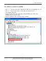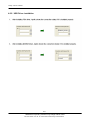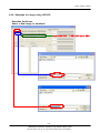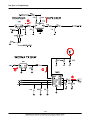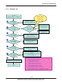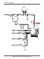
1
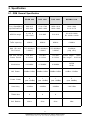
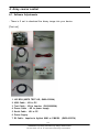
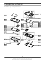
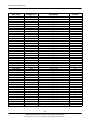
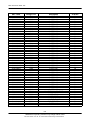
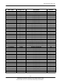
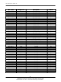
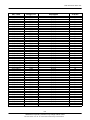
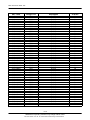
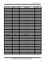
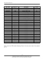
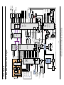
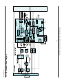
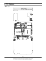
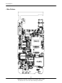
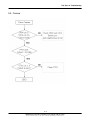
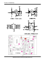
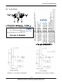
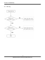
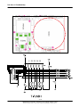
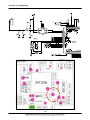
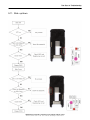
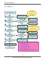
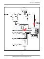
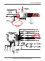
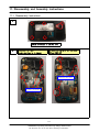
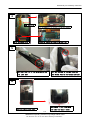
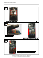
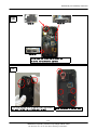
GSM TELEPHONE
SGH-i450
GSM TELEPHONE
CONTENTS
1.
Safety Precautions
2.
Specification
3.
Product Function
4.
Array course control
5.
Exploded View and Parts List
6.
Main Electrical Parts List
7.
Block Diagrams
8.
PCB Diagrams
9.
Flow Chart of Troubleshooting
10.
Reference data
11.
Disassembly and Assembly
Instructions
GSPN (Global Service Partner Network)
Country
North America
Latin America
CIS
Europe
China
Asia
Mideast & Africa
This Service Manual is a property of Samsung Electronics Co.,Ltd.
Any unauthorized use of Manual can be punished under applicable
International and/or domestic law.
Web Site
service.samsungportal.com
latin.samsungportal.com
cis.samsungportal.com
europe.samsungportal.com
china.samsungportal.com
asia.samsungportal.com
mea.samsungportal.com
ⓒ
Samsung Electronics Co.,Ltd.
2007. 10. Rev.1.0
1. Safety Precautions
1-1. Repair Precaution
● Repair in Shield Box, during detailed tuning.
Take specially care of tuning or test, because the specification of cellular phone is sensitive for
surrounding interference(RF noise).
● Be careful to use a kind of magnetic object or tool, because performance of parts is damaged by the
influence of magnetic force.
● Surely use a standard screwdriver when you disassemble this product, otherwise screw will be worn
away.
● Use a thicken twisted wire when you measure level.
A thicken twisted wire has low resistance, therefore error of measurement is few.
● Repair after separate Test Pack and Set because for short danger (for example an
overcurrent and furious flames of parts etc) when you repair board in condition of
connecting Test Pack and tuning on.
● Take specially care of soldering, because Land of PCB is small and weak in heat.
● Surely tune on/off while using AC power plug, because a repair of battery charger is
dangerous when tuning ON/OFF PBA and Connector after disassembling charger.
● Don't use as you pleases after change other material than replacement registered on SEC System.
Otherwise engineer in charge isn't charged with problem that you don't keep this rules.
1-1
SAMSUNG Proprietary-Contents may change without notice
This Document can not be used without Samsung's authorization
Safety Precautions
1-2. ESD(Electrostatically Sensitive Devices) Precaution
Several semiconductor may be damaged easily by static electricity. Such parts are called by ESD
(Electrostatically Sensitive Devices), for example IC,BGA chip etc. Read Precaution below.
You can prevent from ESD damage by static electricity.
● Remove static electricity remained your body before you touch semiconductor or parts with
semiconductor. There are ways that you touch an earthed place or wear static electricity
prevention string on wrist.
● Use earthed soldering steel when you connect or disconnect ESD.
● Use soldering removing tool to break static electricity. , otherwise ESD will be damaged by
static electricity.
● Don't unpack until you set up ESD on product. Because most of ESD are packed by box and
aluminum
plate to have conductive power,they are prevented from static electricity.
● You must maintain electric contact between ESD and place due to be set up until ESD is connected
completely to the proper place or a circuit board.
1-2
SAMSUNG Proprietary-Contents may change without notice
This Document can not be used without Samsung's authorization
2. Specification
2-1. GSM General Specification
EGSM 900
DCS 18 00
PCS 190 0
WCDMA 2100
Fre q. Band[MHz]
Uplink/Downlink
880~91 5
925~96 0
1 710~17 85
1 805~18 80
1 850~19 10
1 930~19 90
1 920~19 80
2 110~21 70
ARFCN r ange
0~124 &
9 75~102 3
512~88 5
512~81 0
UL:9 612~98 88
DL:10 562~10 838
Tx/Rx spa cing
10MHz
20MHz
20MHz
130MHz
Mod. Bit rat e/
Bit Period
27 0.833 kbps
3.692 us
27 0.833 kbps
3.692 us
27 0.833 kbps
3.692 us
3. 84Mcps
(chip ra te)
T ime Slot Per iod/
Fra me Per iod
576.9 us
4. 615ms
576.9 us
4. 615ms
576.9 us
4. 615ms
F rame l ength : 10ms
Slot lengt h : 0. 667ms
Modulation
0.3G M SK
0.3G MSK
0.3G M SK
QPSK
HPSK
MS Powe r
33 dBm~5d Bm
30 dBm~0d Bm
30 dBm~0d Bm
2 4dBm~- 50dBm
Power Class
4
(max +33dBm)
1
(max +30dBm)
1
(max +30dBm)
Sensit ivit y
-1 02dBm
-1 00dBm
-1 00dBm
T DM A Mu x
8
8
8
Cell Radius
35Km
2Km
2Km
2-1
SAMSUNG Proprietary-Contents may change without notice
This Document can not be used without Samsung's authorization
3
(max +24dBm)
- 106.7 dBm
2Km
Specification
2-2. GSM TX power class
TX Power
TX Power
TX Power
control level
GSM850
GSM900
control level
5
33±2 dBm
0
30±3 dBm
0
30±3 dBm
6
31±2 dBm
1
28±3 dBm
1
28±3 dBm
7
29±2 dBm
2
26±3 dBm
2
26±3 dBm
8
27±2 dBm
3
24±3 dBm
3
24±3 dBm
9
25±2 dBm
4
22±3 dBm
4
22±3 dBm
10
23±2 dBm
5
20±3 dBm
5
20±3 dBm
11
21±2 dBm
6
18±3 dBm
6
18±3 dBm
12
19±2 dBm
7
16±3 dBm
7
16±3 dBm
13
17±2 dBm
8
14±3 dBm
8
14±3 dBm
14
15±2 dBm
9
12±4 dBm
9
12±4 dBm
15
13±2 dBm
10
10±4 dBm
10
10±4 dBm
16
11±3 dBm
11
8±4 dBm
11
8±4 dBm
17
9±3 dBm
12
6±4 dBm
12
6±4 dBm
18
7±3 dBm
13
4±4 dBm
13
4±4 dBm
19
5±3 dBm
14
2±5 dBm
14
2±5 dBm
15
0±5 dBm
15
0±5 dBm
DCS1800
control level
2-2
SAMSUNG Proprietary-Contents may change without notice
This Document can not be used without Samsung's authorization
PCS1900
3. Product Function
Main Function
HSDPA/UMTS, EDGE, GPRS
Touch wheel interface for Music UI
Bluetooth v2.0 + EDR
USB v2.0 HS compatible
Camera 2Mega x 16 Digital Zooming and camcorder
FM Radio
Instant Messaging capability
E-mail
Featured applications provide alarms, calendar, calculator, record audio, converter, timer, stopwatch,
and world time.
File viewer (MS office, PDF)
Multimedia Message Service (MMS)
Multimedia capability (with included Media player)
Photo caller ID
Speakerphone capability
WEB/WAP browser (HTMS, xHTML, WML)
3-1
SAMSUNG Proprietary-Contents may change without notice
This Document can not be used without Samsung's authorization
Product Function
3-2
SAMSUNG Proprietary-Contents may change without notice
This Document can not be used without Samsung's authorization
4. Array course control
4-1. Software Adjustments
- There is 2 set to download the binary image into your device.
[First set]
1.
2.
3.
4.
5.
6.
7.
JIG BOX (UMTS TEST JIG; GH80-03308A)
USB Cable : JIG to PC
Test Cable : JIG to Impulse (GH39-00890A)
Power Cable : JIG to power supply
Serial Cable : JIG to PC
Power Supply
Rf Cable : Impulse to Agilent 8960 or CMU200 (GH39-00397A)
4-1
SAMSUNG Proprietary-Contents may change without notice
This Document can not be used without Samsung's authorization
Array course control
[Second Set]
USB Data Link Cable : Impulse to PC (GH39-00922A)
Standard Battery for Impulse (GH43-02985A)
4-2
SAMSUNG Proprietary-Contents may change without notice
This Document can not be used without Samsung's authorization
Array course control
4-2. Software Download
4-2-1. Pre-requisite for Download
SGH - i450 Mobile Device
Apollo v4.01.exe : Downloader Application for SGH-i450
USB Download Driver : SS60_Downloader_Driver.zip
Rom Image : PDA(*.IMG), MODEM(*.BIN) images
Equipment set for Download.
4-3
SAMSUNG Proprietary-Contents may change without notice
This Document can not be used without Samsung's authorization
Array course control
4-2-2. Concupts & cautions.
You can download PDA or MODEM separately. But We are always recommended to
download both at the same time using same version of rom image.
To download an image, the phone need to be set to a proper download mode.
There are 3 download modes.
PDA download : Hold 1, 4 keys and power on -> Blue screen with some information.
MODEM download : Hold 7, * keys and power on -> Blinking "MODEM DOWNLOAD"
on blue screen
All download : Hold 4, 7 keys and power on -> Blinking "ALL DOWNLOAD" on blue screen
For PDA image download, the phone shows download progress on the screen
For MODEM image download, the phone shows RGBW/B Screen.
For All download mode, MODEM image is downloaded first and then PDA
downloading starts.
After downloading PDA, the phone will be reboot.
Do NOT interrupt downloading process or the phone will be damaged. You would be
unable to boot up the phone or to re-flash the phone. Let it finish downloading
process even though you are flashing wrong images.
4-4
SAMSUNG Proprietary-Contents may change without notice
This Document can not be used without Samsung's authorization
Array course control
4-2-3. USB Driver installation for PDA
Execution Apollo.exe.
SGH-i450 connect to the Host computer using download equipment set.
Hold “1+4” key and insert power supplied test cable when use equipment set 1
or Hold “1+4” key and press power on key when use equipment set 2.
Install PDA side driver.
Follow New H/W Installation Manager.
Select ‘IBootHostUSB.inf’file under ‘i450_Apollo_Drivers\PDA_driver’ folder when
Windows asks for new h/w driver. It is safe to choose “Yes” for the waring window.
Confirm “SAMSUNG BlueFin USB Downloader” Installed.
Refer to Next Page.
** If Windows doesn’t ask for USB driver, it means USB driver installation was
failed before. Open Hardware Manager then delete devices with?or!mark then try
again. If it doesn’t work, you need to right click on the device then try Driver
Update.
After installing PDA driver, Apollo shows the connection status if it is installed
properly.
4-5
SAMSUNG Proprietary-Contents may change without notice
This Document can not be used without Samsung's authorization
Array course control
4-6
SAMSUNG Proprietary-Contents may change without notice
This Document can not be used without Samsung's authorization
Array course control
4-2-4. USB Driver installation for MODEM
Hold “7 + *” key and insert power supplied test cable when use equipment set 1 or
Hold “7+ *” key and press power on key when use equipment set 2.
Install Modem side driver.
Execute ‘Setup.exe’file under ‘i450_Apollo_Drivers\PHONE_driver’ folder when
Windows asks for new h/w driver.
Confirm “SAMSUNG USB Composite Device” Installed.
4-7
SAMSUNG Proprietary-Contents may change without notice
This Document can not be used without Samsung's authorization
Array course control
4-2-5. USB Driver installation
4-8
SAMSUNG Proprietary-Contents may change without notice
This Document can not be used without Samsung's authorization
Array course control
4-2-6. Download the image using APOLLO
Execution Apollo.exe.
Select a Rom Image to download
Check this field : 1. SGH-i450 (above GH4^)
4-9
SAMSUNG Proprietary-Contents may change without notice
This Document can not be used without Samsung's authorization
Array course control
Select the proper check option .
PDA stasus
- Bootloader : Update PDA Bootloader section.
- NV Clear : IMEI section erase.
You can see following message when you click this option
MODEM Status
- Boot Update : Update Modem Bootloader section.
4-10
SAMSUNG Proprietary-Contents may change without notice
This Document can not be used without Samsung's authorization
Array course control
Make sure that phone and host computer connection, click proper download
button.
PDA download : Hold 1, 4 keys and power on -> Blue screen with some information.
MODEM download : Hold 7, * keys and power on -> Blinking "MODEM DOWNLOAD"
on blue screen
All download : Hold 4, 7 keys and power on -> Blinking "ALL DOWNLOAD" on blue screen
4-11
SAMSUNG Proprietary-Contents may change without notice
This Document can not be used without Samsung's authorization
Array course control
Do NOT interrupt downloading process.
- Pda download time: About 1 min.
- Modem download time : About 2 min.
- All download time: About 3 min.
Confirm Download Complete.
- SGH-i450 will be reboot when PDA download complete.
4-12
SAMSUNG Proprietary-Contents may change without notice
This Document can not be used without Samsung's authorization
Array course control
4-2-7. Troubleshooting
Unable to install USB driver.
Try another Download equipment
Try another SGH-i450.
Consult to R&D team.
Download stops in the middle.
Close and launch Apollo again then try again.
Check the battery is charged enough.
Download doesn’t start
Check the connection between Apollo and a SGH-i450.
Check the image that is not damaged.
Select an image and download again.
Phone doesn’t boot up after downloading.
Check the release version of PDA and MODEM. They should be same.
Make sure that rom image, and then try to download.
4-13
SAMSUNG Proprietary-Contents may change without notice
This Document can not be used without Samsung's authorization
Array course control
4-14
SAMSUNG Proprietary-Contents may change without notice
This Document can not be used without Samsung's authorization
5. Exploded View and Parts List
5-1. Cellular phone Exploded View
QIF01
QFR01
QMW01
QSD01
QCR58
QFU01
QCR12
QMP01
QMI01
QCK02
QAN05
QVO01
QKP01
QSH03
QCA02
QCA01
QCK01
QSH01
QSH02
QAR01
QSP01
QMO01
QLC01
QRF03
QPC01
QRE01
QFL01
QCR06
QHI01
QCR06
QBA01
QCR12
QFL04
QBA00
5-3
SAMSUNG Proprietary-Contents may change without notice
This Document can not be used without Samsung's authorization
Exploded View and Parts List
5-2. Cellular phone Parts List
Design LOC
Description
SEC CODE
QAN05
ASSY RUBBER-INTENNA
GH98-03392A
QAR01
AUDIO-RECEIVER
3009-001291
QBA00
PMO COVER-BATT(OPEN)
GH72-44609A
QBA01
INNER BATTERY PACK-1140MAH,BLK
GH43-02985A
QCA01
CAMERA MODULE-2M
GH59-04932A
QCA02
CAMERA MODULE-VGA
GH59-04942A
QCK01
PMO KEY-CAMERA
GH72-43303A
QCK02
PMO KEY-POWER
GH72-43305A
QCR06
SCREW-MACHINE
6001-001155
QCR12
SCREW-MACHINE
6001-001530
QCR12
SCREW-MACHINE
6001-001530
QCR58
SCREW-MACHINE
6001-001870
QFL01
ASSY CASE-SLIDE LOWER
GH98-05825A
QFL04
ASSY COVER-DAMPER LOWER
GH98-05983A
QFR01
ASSY CASE-FRONT
GH98-05826A
QFU01
ASSY CASE-SLIDE UPPER(EU)
GH98-06919A
QHI01
ASSY HINGE-PLATE
GH98-05828A
QIF01
PMO COVER-IF
GH72-43297A
QKP01
ASSY KEYPAD-SUB(BLK/OPEN)
GH98-05830A
QLC01
LCD-MODULE, SGHI450
GH07-01220A
QMI01
MICROPHONE-ASSY-SGHI450
GH30-00419A
QMO01
MOTOR DC-SGHI450
GH31-00374A
QMP01
PBA MAIN-SGHI450
GH92-04056A
QMW01
PCT WINDOW-MAIN
GH72-43518A
QPC01
FPC-SGHI450 CABLE
GH41-01920A
QRE01
ASSY CASE-REAR
GH98-05827A
QRF01
TAPE-RF CONNECTOR CAP
GH74-33834A
QRF03
PMO COVER-3.5 EARJACK
GH72-44410A
QSD01
PMO COVER-MICRO SD
GH72-43296A
QSH01
ICT SHIELD-COVER A
GH70-03032A
QSH02
ICT SHIELD-COVER B
GH70-03033A
QSH03
ICT SHIELD-COVER C
GH70-03034A
QSP01
ASSY ETC-SPEAKER MODULE(BLK)
GH59-05235A
QVO01
PMO KEY-VOLUME
GH72-43304A
5-2
SAMSUNG Proprietary-Contents may change without notice
This Document can not be used without Samsung's authorization
Exploded View and Parts List
Description
SEC CODE
CBF INTERFACE-DLC APCBS10BBE(S
GH39-00922A
ADAPTOR-ATADS10EBE,BLK,EU
GH44-01702A
EARPHONE-SGHE210,AAEP405MBE,A
GH59-04535A
IC-MCP
1108-000050
VINYL-BOHO SPK CASE
GH74-36870A
TAPE-SCREW CAP TOP
GH74-33828A
VINYL-BOHO MAIN WINDOW
GH74-35470A
VINYL-BOHO LCD
GH74-36156A
VINYL-BOHO WINDOW 2
GH74-36177A
LABEL(R)-WATER SOAK
GH68-09361A
TAPE INSU
GH74-18422A
TAPE-LCD 2
GH74-36773A
TAPE ELEC-FRONT
GH74-36844A
VINYL-BOHO SPK CASE
GH74-36870A
BAG PE
6902-000634
LABEL(P)-IMEI
GH68-01335D
LABEL(R)-MAIN(EU)
GH68-16413B
CUSHION-CASE(EU)
GH69-05999A
BOX-UNIT(EU)
GH69-06068B
LABEL(P)-UNIT SEAL
GH68-00518B
IC-MEMORY CARD
1109-001363
S/W CD-SGHI450 PC STUDIO CD
GH46-00558A
MANUAL USERS-XEU ENGLISH QRG
GH68-16578A
MANUAL USERS-XEN DUTCH QSG
GH68-16830A
5-3
SAMSUNG Proprietary-Contents may change without notice
This Document can not be used without Samsung's authorization
Exploded View and Parts List
5-4
SAMSUNG Proprietary-Contents may change without notice
This Document can not be used without Samsung's authorization
6. MAIN Electrical Parts List
SEC Code
Design LOC
Description
STATUS
GH71-06262A
GH71-06262A
GH71-06262A
GH71-06721A
4302-001180
3711-006249
2203-000812
2203-005659
2203-005659
2203-005659
2203-005659
2203-000812
2203-000466
2203-000233
2203-000627
2203-000627
2203-006423
2203-000233
2203-000233
2203-005682
2203-000233
2203-000330
2203-000438
2203-006048
2203-000627
2203-000812
2203-001437
2203-005382
2203-005382
2203-005682
2203-006423
2203-001072
2203-006423
2203-000714
2203-002668
2203-000627
2203-005682
2203-005736
2203-000233
2203-006423
2203-005725
2203-005725
2203-000870
2203-006423
2203-001072
2203-000870
2203-006423
2203-000438
2203-006423
2203-006423
2203-000812
2203-000438
2203-006194
ANT101
ANT102
ANT103
ANT104
BAT301
BTC301
C100
C101
C102
C103
C104
C105
C106
C107
C108
C109
C110
C111
C112
C113
C114
C115
C116
C117
C118
C119
C120
C121
C122
C124
C127
C128
C129
C130
C131
C133
C134
C136
C137
C138
C139
C140
C141
C142
C143
C145
C146
C147
C148
C149
C150
C151
C152
NPR-ANTENNA CONTACT V2
NPR-ANTENNA CONTACT V2
NPR-ANTENNA CONTACT V2
NPR-ANT CONTACT
BATTERY-LI(2ND)
HEADER-BATTERY
C-CER,CHIP
C-CER,CHIP
C-CER,CHIP
C-CER,CHIP
C-CER,CHIP
C-CER,CHIP
C-CER,CHIP
C-CER,CHIP
C-CER,CHIP
C-CER,CHIP
C-CER,CHIP
C-CER,CHIP
C-CER,CHIP
C-CER,CHIP
C-CER,CHIP
C-CER,CHIP
C-CER,CHIP
C-CER,CHIP
C-CER,CHIP
C-CER,CHIP
C-CER,CHIP
C-CER,CHIP
C-CER,CHIP
C-CER,CHIP
C-CER,CHIP
C-CER,CHIP
C-CER,CHIP
C-CER,CHIP
C-CER,CHIP
C-CER,CHIP
C-CER,CHIP
C-CER,CHIP
C-CER,CHIP
C-CER,CHIP
C-CER,CHIP
C-CER,CHIP
C-CER,CHIP
C-CER,CHIP
C-CER,CHIP
C-CER,CHIP
C-CER,CHIP
C-CER,CHIP
C-CER,CHIP
C-CER,CHIP
C-CER,CHIP
C-CER,CHIP
C-CER,CHIP
SA
SA
SA
SA
SA
SA
SA
SA
SA
SA
SA
SA
SA
SA
SNA
SNA
SA
SA
SA
SA
SA
SA
SA
SA
SNA
SA
SA
SA
SA
SA
SA
SA
SA
SA
SA
SNA
SA
SA
SA
SA
SA
SA
SA
SA
SA
SA
SA
SA
SA
SA
SA
SA
SA
6-1
SAMSUNG Proprietary-Contents may change without notice
This Document can not be used without Samsung's authorization
Main Electrical Parts List
SEC Code
Design LOC
Description
STATUS
2203-006681
2203-005806
2203-000627
2203-005736
2203-000438
2203-000254
2203-000627
2203-005725
2203-006562
2203-000627
2203-006824
2203-005446
2203-000438
2203-006048
2203-006137
2203-006841
2203-006048
2203-006048
2203-006399
2203-006399
2203-006399
2203-006399
2203-006399
2203-000330
2203-006137
2203-006841
2203-005682
2203-001259
2203-003054
2203-000233
2203-000330
2203-000812
2203-000627
2203-006423
2203-000854
2203-000466
2203-005383
2203-005806
2203-006423
2203-006562
2203-006048
2203-006048
2203-006048
2203-006562
2203-006562
2203-006562
2203-006562
2203-000489
2203-005480
2203-006824
2203-000254
2203-006048
2203-006048
C153
C154
C155
C156
C157
C158
C159
C160
C161
C162
C163
C165
C167
C168
C169
C170
C171
C172
C173
C174
C175
C176
C177
C178
C179
C180
C182
C184
C186
C188
C189
C190
C191
C192
C194
C196
C197
C199
C200
C201
C202
C203
C204
C205
C206
C207
C208
C209
C210
C216
C224
C225
C226
C-CER,CHIP
C-CER,CHIP
C-CER,CHIP
C-CER,CHIP
C-CER,CHIP
C-CER,CHIP
C-CER,CHIP
C-CER,CHIP
C-CER,CHIP
C-CER,CHIP
C-CER,CHIP
C-CER,CHIP
C-CER,CHIP
C-CER,CHIP
C-CER,CHIP
C-CER,CHIP
C-CER,CHIP
C-CER,CHIP
C-CER,CHIP
C-CER,CHIP
C-CER,CHIP
C-CER,CHIP
C-CER,CHIP
C-CER,CHIP
C-CER,CHIP
C-CER,CHIP
C-CER,CHIP
C-CER,CHIP
C-CER,CHIP
C-CER,CHIP
C-CER,CHIP
C-CER,CHIP
C-CER,CHIP
C-CER,CHIP
C-CER,CHIP
C-CER,CHIP
C-CER,CHIP
C-CER,CHIP
C-CER,CHIP
C-CER,CHIP
C-CER,CHIP
C-CER,CHIP
C-CER,CHIP
C-CER,CHIP
C-CER,CHIP
C-CER,CHIP
C-CER,CHIP
C-CER,CHIP
C-CER,CHIP
C-CER,CHIP
C-CER,CHIP
C-CER,CHIP
C-CER,CHIP
SA
SNA
SNA
SA
SA
SA
SNA
SA
SA
SNA
SA
SA
SA
SA
SA
SA
SA
SA
SA
SA
SA
SA
SA
SA
SA
SA
SA
SA
SA
SA
SA
SA
SNA
SA
SA
SA
SA
SNA
SA
SA
SA
SA
SA
SA
SA
SA
SA
SA
SA
SA
SA
SA
SA
6-2
SAMSUNG Proprietary-Contents may change without notice
This Document can not be used without Samsung's authorization
Main Electrical Parts List
SEC Code
Design LOC
Description
STATUS
2203-006562
2203-006872
2203-000995
2203-006562
2203-006562
2203-006048
2203-006048
2203-006048
2203-006562
2203-006825
2203-000254
2203-006048
2203-000254
2203-006048
2203-006048
2203-006562
2203-005482
2203-006048
2203-005482
2203-006562
2203-006423
2203-006838
2203-006824
2203-000233
2203-000330
2203-000330
2203-005482
2203-006841
2203-006841
2203-002709
2203-006474
2203-002709
2203-006208
2203-006208
2203-006838
2203-006208
2203-006208
2203-002709
2203-006824
2203-002709
2203-006824
2203-002709
2203-006841
2203-002709
2203-002709
2203-006048
2203-006260
2203-006053
2203-000189
2203-002709
2203-006824
2203-000330
2203-000330
C227
C228
C229
C238
C239
C248
C249
C251
C253
C255
C256
C257
C259
C261
C262
C264
C268
C272
C274
C279
C290
C301
C302
C303
C304
C305
C306
C313
C314
C315
C316
C317
C318
C319
C320
C321
C322
C323
C324
C325
C326
C330
C343
C344
C345
C346
C360
C362
C363
C364
C365
C410
C411
C-CER,CHIP
C-CER,CHIP
C-CER,CHIP
C-CER,CHIP
C-CER,CHIP
C-CER,CHIP
C-CER,CHIP
C-CER,CHIP
C-CER,CHIP
C-CER,CHIP
C-CER,CHIP
C-CER,CHIP
C-CER,CHIP
C-CER,CHIP
C-CER,CHIP
C-CER,CHIP
C-CER,CHIP
C-CER,CHIP
C-CER,CHIP
C-CER,CHIP
C-CER,CHIP
C-CER,CHIP
C-CER,CHIP
C-CER,CHIP
C-CER,CHIP
C-CER,CHIP
C-CER,CHIP
C-CER,CHIP
C-CER,CHIP
C-CER,CHIP
C-CER,CHIP
C-CER,CHIP
C-CER,CHIP
C-CER,CHIP
C-CER,CHIP
C-CER,CHIP
C-CER,CHIP
C-CER,CHIP
C-CER,CHIP
C-CER,CHIP
C-CER,CHIP
C-CER,CHIP
C-CER,CHIP
C-CER,CHIP
C-CER,CHIP
C-CER,CHIP
C-CER,CHIP
C-CER,CHIP
C-CER,CHIP
C-CER,CHIP
C-CER,CHIP
C-CER,CHIP
C-CER,CHIP
SA
SA
SA
SA
SA
SA
SA
SA
SA
SA
SA
SA
SA
SA
SA
SA
SA
SA
SA
SA
SA
SA
SA
SA
SA
SA
SA
SA
SA
SA
SA
SA
SA
SA
SA
SA
SA
SA
SA
SA
SA
SA
SA
SA
SA
SA
SA
SA
SA
SA
SA
SA
SA
6-3
SAMSUNG Proprietary-Contents may change without notice
This Document can not be used without Samsung's authorization
Main Electrical Parts List
SEC Code
Design LOC
Description
STATUS
2203-006562
2203-006562
2203-005819
2203-005819
2203-006562
2203-005819
2203-006562
2203-006324
2203-006562
2203-006562
2203-006562
2203-006562
2203-005682
2203-006423
2203-006562
2203-006562
2203-006562
2203-006562
2203-006423
2203-006562
2203-003054
2203-003054
2203-003054
2203-000812
2203-000812
2203-000812
2203-006399
2203-005682
2203-006423
2203-006423
2203-006423
2203-000812
2203-000812
2203-000812
2203-003054
2203-003054
2203-003054
2203-000812
2203-000812
2203-005482
2203-000643
2203-000812
2203-000812
2203-006681
2203-006681
2203-006681
2203-006091
2203-006091
2007-009410
2007-009410
2203-006562
2203-001259
2203-000812
C413
C414
C416
C417
C418
C419
C422
C424
C428
C429
C430
C431
C432
C433
C434
C435
C436
C437
C438
C441
C501
C502
C503
C504
C505
C506
C507
C508
C509
C510
C511
C512
C513
C514
C515
C516
C517
C519
C520
C521
C529
C530
C531
C533
C534
C535
C536
C537
C538
C539
C541
C542
C543
C-CER,CHIP
C-CER,CHIP
C-CER,CHIP
C-CER,CHIP
C-CER,CHIP
C-CER,CHIP
C-CER,CHIP
C-CER,CHIP
C-CER,CHIP
C-CER,CHIP
C-CER,CHIP
C-CER,CHIP
C-CER,CHIP
C-CER,CHIP
C-CER,CHIP
C-CER,CHIP
C-CER,CHIP
C-CER,CHIP
C-CER,CHIP
C-CER,CHIP
C-CER,CHIP
C-CER,CHIP
C-CER,CHIP
C-CER,CHIP
C-CER,CHIP
C-CER,CHIP
C-CER,CHIP
C-CER,CHIP
C-CER,CHIP
C-CER,CHIP
C-CER,CHIP
C-CER,CHIP
C-CER,CHIP
C-CER,CHIP
C-CER,CHIP
C-CER,CHIP
C-CER,CHIP
C-CER,CHIP
C-CER,CHIP
C-CER,CHIP
C-CER,CHIP
C-CER,CHIP
C-CER,CHIP
C-CER,CHIP
C-CER,CHIP
C-CER,CHIP
C-CER,CHIP
C-CER,CHIP
R-CHIP
R-CHIP
C-CER,CHIP
C-CER,CHIP
C-CER,CHIP
SA
SA
SA
SA
SA
SA
SA
SA
SA
SA
SA
SA
SA
SA
SA
SA
SA
SA
SA
SA
SA
SA
SA
SA
SA
SA
SA
SA
SA
SA
SA
SA
SA
SA
SA
SA
SA
SA
SA
SA
SA
SA
SA
SA
SA
SA
SA
SA
SA
SA
SA
SA
SA
6-4
SAMSUNG Proprietary-Contents may change without notice
This Document can not be used without Samsung's authorization
Main Electrical Parts List
SEC Code
Design LOC
Description
STATUS
2203-006260
2203-006260
2203-006562
2203-006562
2203-000812
2203-005779
2203-005779
2203-005779
2203-005779
2203-006048
2203-006048
2203-006048
2203-006048
2203-006562
2203-006824
2203-006824
2203-005482
2203-006978
2203-006839
2203-006562
2203-006824
2203-006824
2203-006562
2203-006681
2203-006885
2203-000643
2203-003054
2203-003054
2203-000438
2203-006824
2203-006824
2203-006562
2203-006562
2203-002709
2203-002709
2203-000386
2203-000386
2203-000386
2203-000386
2203-006324
2203-006324
2203-006824
2203-005717
2203-005717
2203-005717
2203-005717
2203-005717
2203-005717
2203-005717
2203-005717
2203-006423
2203-006423
2203-006423
C544
C545
C546
C547
C548
C549
C550
C551
C552
C600
C601
C602
C603
C604
C605
C606
C607
C608
C609
C610
C611
C612
C616
C618
C619
C620
C621
C622
C623
C624
C625
C626
C627
C702
C703
C704
C705
C706
C707
C708
C709
C710
C711
C712
C713
C714
C715
C716
C717
C718
C800
C801
C802
C-CER,CHIP
C-CER,CHIP
C-CER,CHIP
C-CER,CHIP
C-CER,CHIP
C-CER,CHIP
C-CER,CHIP
C-CER,CHIP
C-CER,CHIP
C-CER,CHIP
C-CER,CHIP
C-CER,CHIP
C-CER,CHIP
C-CER,CHIP
C-CER,CHIP
C-CER,CHIP
C-CER,CHIP
C-CER,CHIP
C-CER,CHIP
C-CER,CHIP
C-CER,CHIP
C-CER,CHIP
C-CER,CHIP
C-CER,CHIP
C-CER,CHIP
C-CER,CHIP
C-CER,CHIP
C-CER,CHIP
C-CER,CHIP
C-CER,CHIP
C-CER,CHIP
C-CER,CHIP
C-CER,CHIP
C-CER,CHIP
C-CER,CHIP
C-CER,CHIP
C-CER,CHIP
C-CER,CHIP
C-CER,CHIP
C-CER,CHIP
C-CER,CHIP
C-CER,CHIP
C-CER,CHIP
C-CER,CHIP
C-CER,CHIP
C-CER,CHIP
C-CER,CHIP
C-CER,CHIP
C-CER,CHIP
C-CER,CHIP
C-CER,CHIP
C-CER,CHIP
C-CER,CHIP
SA
SA
SA
SA
SA
SA
SA
SA
SA
SA
SA
SA
SA
SA
SA
SA
SA
SA
SA
SA
SA
SA
SA
SA
SA
SA
SA
SA
SA
SA
SA
SA
SA
SA
SA
SA
SA
SA
SA
SA
SA
SA
SA
SA
SA
SA
SA
SA
SA
SA
SA
SA
SA
6-5
SAMSUNG Proprietary-Contents may change without notice
This Document can not be used without Samsung's authorization
Main Electrical Parts List
SEC Code
Design LOC
Description
STATUS
2203-006423
2203-006423
2203-006423
2203-006423
2203-006423
2203-006423
2203-006423
2203-006423
2203-006423
2203-006423
2203-006423
2203-006423
2203-006423
2203-006423
2203-006423
2203-006423
2203-006423
2203-006423
2203-006423
2203-005482
2203-006423
2203-006825
2203-006423
2203-006423
2203-006423
2203-006562
2203-006562
2203-006423
2203-006423
2203-006423
2203-006423
2203-006423
2203-006423
2203-006423
2203-006423
2203-006423
2203-006423
2203-006562
2203-006562
2203-006562
2203-006423
2203-006423
2203-006423
2203-006423
3709-001392
0407-001002
0407-001002
0403-001547
0407-001007
3722-002609
2911-000091
2904-001703
2904-001629
C803
C804
C805
C806
C807
C808
C809
C810
C816
C817
C818
C819
C820
C821
C822
C823
C824
C825
C826
C839
C840
C841
C842
C843
C852
C853
C854
C855
C856
C857
C858
C859
C860
C861
C862
C863
C864
C865
C900
C901
C902
C903
C904
C905
CD301
D301
D600
D601
D603
EAR501
F101
F102
F103
C-CER,CHIP
C-CER,CHIP
C-CER,CHIP
C-CER,CHIP
C-CER,CHIP
C-CER,CHIP
C-CER,CHIP
C-CER,CHIP
C-CER,CHIP
C-CER,CHIP
C-CER,CHIP
C-CER,CHIP
C-CER,CHIP
C-CER,CHIP
C-CER,CHIP
C-CER,CHIP
C-CER,CHIP
C-CER,CHIP
C-CER,CHIP
C-CER,CHIP
C-CER,CHIP
C-CER,CHIP
C-CER,CHIP
C-CER,CHIP
C-CER,CHIP
C-CER,CHIP
C-CER,CHIP
C-CER,CHIP
C-CER,CHIP
C-CER,CHIP
C-CER,CHIP
C-CER,CHIP
C-CER,CHIP
C-CER,CHIP
C-CER,CHIP
C-CER,CHIP
C-CER,CHIP
C-CER,CHIP
C-CER,CHIP
C-CER,CHIP
C-CER,CHIP
C-CER,CHIP
C-CER,CHIP
C-CER,CHIP
CONNECTOR-CARD EDGE
DIODE-ARRAY
DIODE-ARRAY
DIODE-ZENER
DIODE-ARRAY
JACK-EAR PHONE
DUPLEXER-FEM
FILTER-SAW
FILTER-SAW
SA
SA
SA
SA
SA
SA
SA
SA
SA
SA
SA
SA
SA
SA
SA
SA
SA
SA
SA
SA
SA
SA
SA
SA
SA
SA
SA
SA
SA
SA
SA
SA
SA
SA
SA
SA
SA
SA
SA
SA
SA
SA
SA
SA
SA
SA
SA
SA
SA
SA
SA
SA
SA
6-6
SAMSUNG Proprietary-Contents may change without notice
This Document can not be used without Samsung's authorization
Main Electrical Parts List
SEC Code
Design LOC
Description
STATUS
2910-000024
4709-001399
2904-001702
4709-001543
2901-001353
2901-001353
2901-001353
2901-001353
2901-001353
2901-001353
2901-001353
2901-001353
GH70-02640A
GH70-02640A
GH70-02640A
GH70-02640A
GH70-02640A
GH70-02640A
GH70-02640A
GH70-02640A
GH70-02640A
GH70-02640A
GH70-02640A
GH70-02640A
GH70-02640A
GH70-02640A
GH70-02640A
3711-005945
3711-005643
3711-005550
3711-005550
3710-002499
2703-002202
2703-001180
2703-002281
2703-002204
2703-002281
2703-002281
2703-002200
2703-002281
2703-002202
2703-001752
2703-002202
2703-002367
2703-001749
2703-002367
2703-002208
2703-002369
2703-002199
2703-002368
3301-001756
2703-002208
2703-002367
F104
F105
F106
F107
F700
F701
F702
F703
F704
F705
F706
F707
FPC100
FPC101
FPC102
FPC103
FPC104
FPC105
FPC106
FPC107
FPC108
FPC109
FPC110
FPC111
FPC112
FPC113
FPC114
HDC700
HDC701
HDC702
HDC703
IFC600
L101
L102
L103
L104
L105
L106
L107
L108
L109
L110
L111
L112
L113
L114
L115
L116
L117
L120
L125
L129
L132
DUPLEXER-SAW
COUPLER-DIRECTION
FILTER-SAW
BALUN
FILTER-EMI/ESD
FILTER-EMI/ESD
FILTER-EMI/ESD
FILTER-EMI/ESD
FILTER-EMI/ESD
FILTER-EMI/ESD
FILTER-EMI/ESD
FILTER-EMI/ESD
ICT SHIELD-CAN CLIP
ICT SHIELD-CAN CLIP
ICT SHIELD-CAN CLIP
ICT SHIELD-CAN CLIP
ICT SHIELD-CAN CLIP
ICT SHIELD-CAN CLIP
ICT SHIELD-CAN CLIP
ICT SHIELD-CAN CLIP
ICT SHIELD-CAN CLIP
ICT SHIELD-CAN CLIP
ICT SHIELD-CAN CLIP
ICT SHIELD-CAN CLIP
ICT SHIELD-CAN CLIP
ICT SHIELD-CAN CLIP
ICT SHIELD-CAN CLIP
HEADER-BOARD TO BOARD
HEADER-BOARD TO BOARD
HEADER-BOARD TO BOARD
HEADER-BOARD TO BOARD
SOCKET-INTERFACE
INDUCTOR-SMD
INDUCTOR-SMD
INDUCTOR-SMD
INDUCTOR-SMD
INDUCTOR-SMD
INDUCTOR-SMD
INDUCTOR-SMD
INDUCTOR-SMD
INDUCTOR-SMD
INDUCTOR-SMD
INDUCTOR-SMD
INDUCTOR-SMD
INDUCTOR-SMD
INDUCTOR-SMD
INDUCTOR-SMD
INDUCTOR-SMD
INDUCTOR-SMD
INDUCTOR-SMD
BEAD-SMD
INDUCTOR-SMD
INDUCTOR-SMD
SA
SA
SA
SA
SA
SA
SA
SA
SA
SA
SA
SA
SA
SA
SA
SA
SA
SA
SA
SA
SA
SA
SA
SA
SA
SA
SA
SA
SA
SA
SA
SA
SA
SA
SA
SA
SA
SA
SA
SA
SA
SA
SA
SA
SA
SA
SA
SA
SA
SA
SA
SA
SA
6-7
SAMSUNG Proprietary-Contents may change without notice
This Document can not be used without Samsung's authorization
Main Electrical Parts List
SEC Code
Design LOC
Description
STATUS
2703-002367
2703-002281
2703-002281
2703-001178
2703-002782
2703-002782
2703-002782
2703-002814
2703-002814
3301-001438
3301-001438
3301-001438
3301-001438
3301-001438
2703-002313
3301-001158
3301-001158
3301-001342
3301-001342
2703-002313
2703-002368
2703-002368
1205-003169
2801-004455
2801-004466
2801-004466
2804-001736
1201-002446
1201-002531
2007-000172
2007-003020
2007-000171
2007-000171
2007-000171
2007-000171
2007-008542
2007-000174
2007-008542
2007-003015
2007-007193
2007-001305
2007-001305
2007-008542
2007-007309
2007-003015
2007-007193
2007-008544
2007-007798
2007-009801
2007-000141
2007-001298
2007-001305
2007-001305
L133
L134
L135
L136
L301
L302
L307
L401
L402
L501
L502
L503
L504
L505
L506
L507
L508
L600
L601
L602
L603
L604
MOD100
OSC100
OSC301
OSC400
OSC401
PAM100
PAM101
R100
R1002
R101
R102
R103
R105
R107
R109
R110
R111
R112
R113
R114
R116
R117
R119
R125
R126
R127
R128
R129
R130
R132
R133
INDUCTOR-SMD
INDUCTOR-SMD
INDUCTOR-SMD
INDUCTOR-SMD
INDUCTOR-SMD
INDUCTOR-SMD
INDUCTOR-SMD
INDUCTOR-SMD
INDUCTOR-SMD
BEAD-SMD
BEAD-SMD
BEAD-SMD
BEAD-SMD
BEAD-SMD
INDUCTOR-SMD
BEAD-SMD
BEAD-SMD
BEAD-SMD
BEAD-SMD
INDUCTOR-SMD
INDUCTOR-SMD
INDUCTOR-SMD
IC-DATA COMM./GEN.
CRYSTAL-SMD
CRYSTAL-SMD
CRYSTAL-SMD
OSCILLATOR-CLOCK
IC-POWER AMP
IC-POWER AMP
R-CHIP
R-CHIP
R-CHIP
R-CHIP
R-CHIP
R-CHIP
R-CHIP
R-CHIP
R-CHIP
R-CHIP
R-CHIP
R-CHIP
R-CHIP
R-CHIP
R-CHIP
R-CHIP
R-CHIP
R-CHIP
R-CHIP
R-CHIP
R-CHIP
R-CHIP
R-CHIP
R-CHIP
SA
SA
SA
SA
SA
SA
SA
SA
SA
SA
SA
SA
SA
SA
SA
SA
SA
SA
SA
SA
SA
SA
SA
SA
SA
SA
SA
SA
SA
SA
SA
SA
SA
SA
SA
SA
SA
SA
SA
SA
SA
SA
SA
SA
SA
SA
SA
SA
SA
SA
SA
SA
SA
6-8
SAMSUNG Proprietary-Contents may change without notice
This Document can not be used without Samsung's authorization
Main Electrical Parts List
SEC Code
Design LOC
Description
STATUS
2007-008806
2007-007009
2007-000138
2007-000138
2007-009801
2007-008542
2007-008542
2007-000161
2007-001290
2007-000148
2007-000137
2007-001298
2007-000148
2007-000148
2007-007316
2007-001292
2007-000170
2007-007107
2007-007107
2007-000070
2007-000157
2007-008213
2007-008043
2007-007468
2007-009171
2007-009171
2007-000157
2007-000157
2007-000157
2007-000157
2007-000157
2007-000157
2007-000162
2007-008806
2007-008806
2007-008806
2007-008806
2007-008806
2007-008806
2007-007142
2007-000162
2007-000162
2007-007316
2007-001119
2007-007766
2007-007132
2007-000165
2007-008055
2007-008055
2007-000162
2007-000143
2007-000143
2007-000162
R135
R138
R139
R140
R143
R148
R149
R152
R200
R207
R209
R222
R226
R229
R239
R241
R246
R251
R252
R300
R305
R307
R308
R312
R313
R316
R321
R322
R323
R324
R325
R326
R327
R328
R329
R330
R331
R332
R333
R338
R381
R382
R383
R384
R385
R389
R390
R401
R402
R403
R408
R409
R410
R-CHIP
R-CHIP
R-CHIP
R-CHIP
R-CHIP
R-CHIP
R-CHIP
R-CHIP
R-CHIP
R-CHIP
R-CHIP
R-CHIP
R-CHIP
R-CHIP
R-CHIP
R-CHIP
R-CHIP
R-CHIP
R-CHIP
R-CHIP
R-CHIP
R-CHIP
R-CHIP
R-CHIP
R-CHIP
R-CHIP
R-CHIP
R-CHIP
R-CHIP
R-CHIP
R-CHIP
R-CHIP
R-CHIP
R-CHIP
R-CHIP
R-CHIP
R-CHIP
R-CHIP
R-CHIP
R-CHIP
R-CHIP
R-CHIP
R-CHIP
R-CHIP
R-CHIP
R-CHIP
R-CHIP
R-CHIP
R-CHIP
R-CHIP
R-CHIP
R-CHIP
R-CHIP
SA
SA
SA
SA
SA
SA
SA
SA
SA
SA
SA
SA
SA
SA
SA
SA
SA
SA
SA
SA
SA
SA
SA
SA
SA
SA
SA
SA
SA
SA
SA
SA
SA
SA
SA
SA
SA
SA
SA
SA
SA
SA
SA
SA
SA
SA
SA
SA
SA
SA
SA
SA
SA
6-9
SAMSUNG Proprietary-Contents may change without notice
This Document can not be used without Samsung's authorization
Main Electrical Parts List
SEC Code
Design LOC
Description
STATUS
2007-000159
2007-001298
2007-000141
2007-008544
2007-008478
2007-008478
2007-008544
2007-008137
2007-008137
2007-000165
2007-000170
2007-000169
2007-000170
2007-000170
2007-008275
2007-008275
2007-003029
2007-001298
2007-001298
2007-009793
2007-009793
2007-000164
2007-000164
2007-001298
2007-000171
2007-001298
2007-007107
2007-007107
2007-008419
2007-008419
2007-008419
2007-008055
2007-007981
2007-000170
2007-008045
2007-008045
2007-001308
2007-007306
2007-007306
2007-008672
2007-007312
2007-007090
2007-001339
2007-001339
2007-009408
2007-009408
2007-007190
2007-000143
2007-000143
2007-000143
2007-000143
2007-007190
2007-008419
R411
R412
R413
R503
R504
R505
R506
R510
R511
R512
R514
R515
R516
R517
R518
R519
R520
R521
R522
R524
R525
R600
R601
R602
R603
R604
R609
R610
R614
R615
R616
R617
R618
R621
R622
R623
R702
R703
R704
R705
R710
R711
R712
R713
R800
R801
R802
R804
R805
R806
R807
R809
R815
R-CHIP
R-CHIP
R-CHIP
R-CHIP
R-CHIP
R-CHIP
R-CHIP
R-CHIP
R-CHIP
R-CHIP
R-CHIP
R-CHIP
R-CHIP
R-CHIP
R-CHIP
R-CHIP
R-CHIP
R-CHIP
R-CHIP
R-CHIP
R-CHIP
R-CHIP
R-CHIP
R-CHIP
R-CHIP
R-CHIP
R-CHIP
R-CHIP
R-CHIP
R-CHIP
R-CHIP
R-CHIP
R-CHIP
R-CHIP
R-CHIP
R-CHIP
R-CHIP
R-CHIP
R-CHIP
R-CHIP
R-CHIP
R-CHIP
R-CHIP
R-CHIP
R-CHIP
R-CHIP
R-CHIP
R-CHIP
R-CHIP
R-CHIP
R-CHIP
R-CHIP
R-CHIP
SA
SA
SA
SA
SA
SA
SA
SA
SA
SA
SA
SA
SA
SA
SA
SA
SA
SA
SA
SA
SA
SA
SA
SA
SA
SA
SA
SA
SA
SA
SA
SA
SA
SA
SA
SA
SA
SA
SA
SA
SA
SA
SA
SA
SA
SA
SA
SA
SA
SA
SA
SA
SA
6-10
SAMSUNG Proprietary-Contents may change without notice
This Document can not be used without Samsung's authorization
Main Electrical Parts List
SEC Code
Design LOC
Description
STATUS
2007-000171
2007-000171
2007-000162
2007-000162
2007-000162
2007-000162
3705-001421
3709-001400
2404-001381
2404-001496
2404-001415
2404-001415
2404-001339
2404-001381
2404-001381
2404-001415
2404-001381
2404-001352
2404-001381
2404-001381
2404-001347
2404-001347
2404-001381
2404-001381
3404-001317
3404-001303
3404-001303
3404-001303
2809-001280
1404-001221
0504-000168
0504-000168
0505-001165
0504-000168
1205-003285
1204-002700
0801-003052
0801-002294
1205-002767
1001-001401
1203-004926
1203-004838
1203-004430
0406-001200
0406-001200
1203-004621
1001-001461
1203-004464
0801-003129
1001-001362
1001-001436
1201-002180
1201-002240
R900
R902
R905
R906
R907
R908
RFS101
SIM301
TA102
TA103
TA401
TA402
TA403
TA404
TA405
TA406
TA407
TA501
TA502
TA503
TA600
TA601
TA800
TA801
TAC700
TAC701
TAC702
TAC703
TCX101
TH200
TR301
TR302
TR600
TR601
U101
U103
U200
U201
U202
U203
U301
U303
U304
U306
U307
U400
U402
U403
U404
U501
U502
U503
U504
R-CHIP
R-CHIP
R-CHIP
R-CHIP
R-CHIP
R-CHIP
CONNECTOR-COAXIAL
CONNECTOR-CARD EDGE
C-TA,CHIP
C-TA,CHIP
C-TA,CHIP
C-TA,CHIP
C-TA,CHIP
C-TA,CHIP
C-TA,CHIP
C-TA,CHIP
C-TA,CHIP
C-TA,CHIP
C-TA,CHIP
C-TA,CHIP
C-TA,CHIP
C-TA,CHIP
C-TA,CHIP
C-TA,CHIP
SWITCH-TACT
SWITCH-TACT
SWITCH-TACT
SWITCH-TACT
OSCILLATOR-VCTCXO
THERMISTOR-NTC
TR-DIGITAL
TR-DIGITAL
FET-SILICON
TR-DIGITAL
IC-TRANSCEIVER
IC-TUNER
IC-CMOS LOGIC
IC-CMOS LOGIC
IC-SWITCH
IC-ANALOG SWITCH
IC-POWER SUPERVISOR
IC-BATTERY
IC-VOL. DETECTOR
DIODE-TVS
DIODE-TVS
IC-POWER SUPERVISOR
IC-ANALOG SWITCH
IC-VOL. DETECTOR
IC-CMOS LOGIC
IC-ANALOG SWITCH
IC-ANALOG SWITCH
IC-AUDIO AMP
IC-AUDIO AMP
SA
SA
SA
SA
SA
SA
SA
SA
SA
SA
SA
SA
SA
SA
SA
SA
SA
SA
SA
SA
SA
SA
SA
SA
SA
SA
SA
SA
SA
SA
SA
SA
SA
SA
SA
SA
SA
SA
SA
SA
SA
SA
SA
SA
SA
SA
SA
SA
SA
SA
SA
SA
SA
6-11
SAMSUNG Proprietary-Contents may change without notice
This Document can not be used without Samsung's authorization
Main Electrical Parts List
SEC Code
Design LOC
Description
STATUS
1202-001068
1203-003737
1203-004607
1009-001027
1009-001027
1203-004120
1203-004249
1001-001336
1203-002716
0801-003016
0801-003012
0801-002294
1203-003643
1006-001322
0801-002321
1203-004956
1205-003215
0904-002295
1108-000127
1106-001511
0406-001223
0406-001223
0406-001223
0406-001223
0406-001223
0406-001223
0406-001223
0406-001223
0406-001223
0406-001197
0406-001197
0406-001190
0406-001190
0406-001223
0406-001223
0406-001223
0406-001223
0406-001223
0406-001223
0406-001223
0406-001223
1108-000050
U505
U600
U601
U602
U603
U604
U606
U607
U608
U609
U610
U611
U612
U701
U900
U903
UCP201
UCP800
UME200
UME900
ZD501
ZD502
ZD503
ZD504
ZD505
ZD506
ZD507
ZD600
ZD601
ZD609
ZD610
ZD700
ZD701
ZD702
ZD703
ZD704
ZD705
ZD706
ZD707
ZD708
ZD709
IC-VOLTAGE COMP.
IC-POSI.FIXED REG.
IC-MULTI REG.
IC-HALL EFFECT S/W
IC-HALL EFFECT S/W
IC-MULTI REG.
IC-MULTI REG.
IC-ANALOG SWITCH
IC-VOL. DETECTOR
IC-CMOS LOGIC
IC-CMOS LOGIC
IC-CMOS LOGIC
IC-MULTI REG.
IC-LINE TRANSCEIVER
IC-CMOS LOGIC
IC-DC/DC CONVERTER
IC-MODEM
IC-DSP
IC-MCP
IC-SRAM
DIODE-TVS
DIODE-TVS
DIODE-TVS
DIODE-TVS
DIODE-TVS
DIODE-TVS
DIODE-TVS
DIODE-TVS
DIODE-TVS
DIODE-TVS
DIODE-TVS
DIODE-TVS
DIODE-TVS
DIODE-TVS
DIODE-TVS
DIODE-TVS
DIODE-TVS
DIODE-TVS
DIODE-TVS
DIODE-TVS
DIODE-TVS
IC-MCP
SA
SA
SA
SA
SA
SA
SA
SA
SA
SA
SA
SA
SA
SA
SA
SA
SA
SA
SA
SA
SA
SA
SA
SA
SA
SA
SA
SA
SA
SA
SA
SA
SA
SA
SA
SA
SA
SA
SA
SA
SA
SA
Please consult the GSPN website (Samsung Portal) for the most recent version of the product's
part list.
6-12
SAMSUNG Proprietary-Contents may change without notice
This Document can not be used without Samsung's authorization
PWR SW
PS_HOLD_PU
SYSEN
Back-Up
Battery
UMTS
RTR6275
TRx
V_BAT
TCXO
19.2MHz
LOAD
S/W
VBUS
NAND 1Gbit
SDRAM 512 Mb
PDA MEM
PHONE_ON
USB I/F
SIM I/F
SBI I/F
TCXO_EN
PM_INT_N
PS_HOLD_F
TCXO_OUT
AMUX_OUT
SLEEP_CLK
REF_OUT
VREG_MSMC_1.2V
VREG_MSME_1.8V
I2S
SPK
AMP
PWRON
MIC
Filter
2431
ADC
26 MHz
TWL4030
VGA_STBY
2M_STBY
I2C I/F
CAM_I/F
MLCD_ON
MLCD_RST
SPI I/F
RGB_I/F
TF_DETECT
EAR
AMP
EAR
SW
FM Radio
KBR(0:3)
KBC(4:6)
KBC(3)
KBR(0:1)
FM_ANT
PCM I/F
S/W
BRF6350
BT
T-Flash
S20
CON.
3.5mm
Earjack
SLID KEY
C
KEYPAD/
VOL SW
Balun
Touch Wheel Key
DOWN HALL IC
RCV
SPK
MOTOR
MOTOR_EN
UP HALL IC
VGA
2M
CAMERA
VPLL1
VTF30
VDD1
KBC(0:2)
VIO
LCD
320x240
QVGA
SQ3D02600B2IBA
I2S 26MHz
BT_RXD/TXD
BT_RTS/CTS
CMD,DAT, CLK
PWR_I2C
CODEC
&
PDA
PMIC
PCM
USB 2.0 HS
USB HS
USB
UART
This Document can not be used without Samsung's authorization
SAMSUNG Proprietary-Contents may change without notice
7-1
VBAT
V_EXT_FET
ON_SW
RCV
SPK
MIC
MIC
SW
PCM I/F
I2S
S/W
32.768kHz
FONE_ON30
nMSM_RST
PON_RESET_N
EAR_KEY, nJACK_INT
PHONE_ON
FONE_RST
PDA_ACTIVE_MSM
TA Earphone DLC
S20 IF CON
UART
S/W
USB
USB
S/W
PCM
UART
SIM
SBI
MSM6260
PDA_ACTIVE30
nINT_DPRAM
OMAP
PHONE_ACTIVE
16KByte
DPRAM
GPMC_D(0:15)
GPMC_A(1:13)
PWR_DET
VREG_MSMA_2.6V
nINT_DPRAM_MSM
A2(1:13)
D2(0:15)
Voltage
Detector
CPU
MODEM
D2(0:15)
D2(0:7)
VBAT
VREG_MSMP_2.6V
Tx I/Q
Rx I/Q
D1(0:31)
NAND 512Mbit
SDRAM 256Mbit
PHONE MEM
A1(0:12)
VREG_MSMP_2.6V
VREG_MSME_1.8V
TA_nCONNECTED, USB_DETECT, TA_OFF, CHG_ING_N
VBUS_FET
VF
V_EXT
V_BAT
VBAT
USB
MAIN
BATTERY
S/W
SIM
SBI
PM6650
PHONE
PMIC
V_EXT_FET
V_BAT
CHHARGING
IC
ON_SW
BKBT
SIM I/F
32.768kHz
VREG_SYNT_2.6V
VREG_TCXO_2.8V
VREG_MSMP_2.6V
RF_SMPS_2.6V
GSM/DCS/PCS
GSM
PAM
UMTS
PAM
V_EXT_FET
IF_CON_SENSE
VREG_TCXO_2.8V
USIM
* GSM
Rx : 925 ~ 960MHz
Tx : 880 ~ 915MHz
* DCS
Rx : 1805 ~ 1880MHz
Tx : 1710 ~ 1785MHz
* PCS
Rx : 1930 ~ 1990MHz
Tx : 1850 ~ 1910MHz
* UMTS
Rx : 2110 ~ 2170MHz
Tx : 1920 ~ 1980MHz
FEM
Dplx
RF BLOCK
7-1. Base Band Solution Block Diagram
7. Block Diagrams
WIRED
OR
SAMSUNG Proprietary-Contents may change without notice
7-2
This Document can not be used without Samsung's authorization
7-2. RF Solution Block Diagram
Block Diagrams
8. PCB Diagrams
- Main Top
8-1
SAMSUNG Proprietary-Contents may change without notice
This Document can not be used without Samsung's authorization
PCB Diagrams
- Main Bottom
8-2
SAMSUNG Proprietary-Contents may change without notice
This Document can not be used without Samsung's authorization
9. Flow Chart of Troubleshooting
9-1. Power On operation
9-1
SAMSUNG Proprietary-Contents may change without notice
This Document can not be used without Samsung's authorization
Flow Chart of Troubleshooting
V_BAT
VREG_TCXO_2.8V
TR600
D600
V_EXT_DIODE
2
D601
TA600
3
R621
1
D603
5
1
1
4
SYSEN
3
2
2
ON_SW
3
IF_CON_SENSE
6
5
2
1
4
VIO
PS_HOLD_PU
VBAT
1
3
TR601
4
2
5
U611
9-2
SAMSUNG Proprietary-Contents may change without notice
This Document can not be used without Samsung's authorization
G
3
TA601
Flow Chart of Troubleshooting
9-2. Initial Operation
9-3
SAMSUNG Proprietary-Contents may change without notice
This Document can not be used without Samsung's authorization
Flow Chart of Troubleshooting
9-4
SAMSUNG Proprietary-Contents may change without notice
This Document can not be used without Samsung's authorization
Flow Chart of Troubleshooting
9-3. Sound Operation
9-5
SAMSUNG Proprietary-Contents may change without notice
This Document can not be used without Samsung's authorization
Flow Chart of Troubleshooting
9-6
SAMSUNG Proprietary-Contents may change without notice
This Document can not be used without Samsung's authorization
Flow Chart of Troubleshooting
9-4. Sound On Calling
9-7
SAMSUNG Proprietary-Contents may change without notice
This Document can not be used without Samsung's authorization
Flow Chart of Troubleshooting
9-8
SAMSUNG Proprietary-Contents may change without notice
This Document can not be used without Samsung's authorization
Flow Chart of Troubleshooting
9-5. Camera
9-9
SAMSUNG Proprietary-Contents may change without notice
This Document can not be used without Samsung's authorization
Flow Chart of Troubleshooting
9-10
SAMSUNG Proprietary-Contents may change without notice
This Document can not be used without Samsung's authorization
Flow Chart of Troubleshooting
9-6. Touch-Wheel
3 GPIOs
2 ADCs
<The part of TWL4030>
< The part of OMAP2431 >
9-11
SAMSUNG Proprietary-Contents may change without notice
This Document can not be used without Samsung's authorization
Flow Chart of Troubleshooting
9-7. 3X4 Key
9-12
SAMSUNG Proprietary-Contents may change without notice
This Document can not be used without Samsung's authorization
Flow Chart of Troubleshooting
9-8. Micro SD card
9-13
SAMSUNG Proprietary-Contents may change without notice
This Document can not be used without Samsung's authorization
Flow Chart of Troubleshooting
9-14
SAMSUNG Proprietary-Contents may change without notice
This Document can not be used without Samsung's authorization
Flow Chart of Troubleshooting
9-9. LCD
9-15
SAMSUNG Proprietary-Contents may change without notice
This Document can not be used without Samsung's authorization
Flow Chart of Troubleshooting
9-16
SAMSUNG Proprietary-Contents may change without notice
This Document can not be used without Samsung's authorization
Flow Chart of Troubleshooting
9-10. BT
9-17
SAMSUNG Proprietary-Contents may change without notice
This Document can not be used without Samsung's authorization
Flow Chart of Troubleshooting
9-18
SAMSUNG Proprietary-Contents may change without notice
This Document can not be used without Samsung's authorization
Flow Chart of Troubleshooting
9-11. Slide up/down
9-19
SAMSUNG Proprietary-Contents may change without notice
This Document can not be used without Samsung's authorization
Flow Chart of Troubleshooting
9-12. WCDMA TX
Pin#6: High
TX ON
Target Power = 23dBm
①
Pin#5: Low
Yes
F101 pin11
>=10 dBm
Pin#4: High
Resolder RFS101,
C105,L101,R105,L132
No
②
Yes
F101 pin9
>=8 dBm
No
Check F101
truth table
Yes
No
③
Yes
F104 pin7
>=5 dBm
④
PAM101 pin8
>=-15 dBm
Pin#3(VENA)=H
Check
UCP201
No
Check
Operating
mode
Yes
Yes
No
Yes
F103 pin1
>-30dBm
No
Check U101 & UCP201
END
Pin#4(VMode1)=L
Check UCP201
No
⑦
Pin#3(VMode2)=L
⑧
Yes
PAM101 pin2
>=-30 dBm
⑥
Resolder or Change
F101
Resolder or Change F104,
C165,C197,L129
No
⑤
Check R107,R110,
R116,UCP201(MSM)
Check VBAT or
Resolder or Change
PAM101
Resolder or change
F103,L120
1.
Check FEM(F101) output
2.
Check FEM(F101) input
3.
Check Duplexer(F104)
4.
Check PAM(PAM101) output
5.
Check PAM(PAM101) input
6.
Check Tx Filter(F103) input
7.
Check RTR6275(U101), MSM6260(UCP201)
9-20
SAMSUNG Proprietary-Contents may change without notice
This Document can not be used without Samsung's authorization
Flow Chart of Troubleshooting
①
②
9-21
SAMSUNG Proprietary-Contents may change without notice
This Document can not be used without Samsung's authorization
Flow Chart of Troubleshooting
③
⑥
⑤
④
9-22
SAMSUNG Proprietary-Contents may change without notice
This Document can not be used without Samsung's authorization
Flow Chart of Troubleshooting
9-13. WCDMA RX
RX ON
Sector Power = -50dBm
Pin#6: High
Pin#5: Low
①
No
F101 pin11
>=-65dBm
Pin#4: High
Resolder RFS101,
C105,L101,R105,L132
Yes
②
Check R107,R110,
No
F101 pin9
>=-70 dBm
No
Check F101
truth table
R116,UCP201
Yes
③
No
F104 pin5
>=-75 dBm
④
Resolder or Change F104,
C165,C197,L129
Yes
No
Resolder or Change
R103,C106
U101 pin26
>=-75 dBm
Yes
⑤
No
U101 pin29
>=-75 dBm
Resolder or Change
U101
Yes
⑥
Resolder or
Change F101
Yes
No
U101 pin34,35
>-75dBm
⑦
Yes
Check U101 & UCP201
END
⑧
Check
C141,C145,C144,L112,L114,F106
,L117,C143,L113
1.
Check FEM(F101) input
2.
Check FEM(F101) output
3.
Check Duplexer(F104)
4.
Check RTR6275(U101) input
5.
Check RTR6275(U101) output
6.
Check RTR6275(U101) I/Q input
7.
Check RTR6275(U101) , MSM6260 (UCP201)
9-23
SAMSUNG Proprietary-Contents may change without notice
This Document can not be used without Samsung's authorization
Flow Chart of Troubleshooting
①
②
9-24
SAMSUNG Proprietary-Contents may change without notice
This Document can not be used without Samsung's authorization
Flow Chart of Troubleshooting
9-25
SAMSUNG Proprietary-Contents may change without notice
This Document can not be used without Samsung's authorization
Flow Chart of Troubleshooting
9-14. EGSM TX
TX ON (PCL 5 level)
Pin#6: High
Pin#5: Low
①
②
Yes
F101 pin11
>=5 dBm
Pin#4: Low
Resolder RFS101,
C105,L101,R105,L132
Check
R107,R110,
R116,UCP201
No
Yes
F101 pin17
>=5 dBm
Check
F101 truth
table
No
Resolder or
Change F101
Yes
No
③
PAM100 pin9
Yes
>=5 dBm
No
④
Yes
PAM100 pin7
>=-30 dBm
Resolder or Change
F101,C100,L115
⑦
Check Vramp
Check
Operating
mode
No
Pin#3(BS)=L
No
OK
No
Pin#1(EN)=H
Yes
Resolder PAM100,
Check UCP201
Check VBAT or
Resolder / Change
PAM100
Resolder or change
R129,UCP201
⑤
Check U101
END
1.
Check FEM(F101) output
2.
Check FEM(F101) input
3.
Check PAM(PAM100) output
4.
Check PAM(PAM100) input
5.
Check RTR6275(U101)
9-26
SAMSUNG Proprietary-Contents may change without notice
This Document can not be used without Samsung's authorization
Flow Chart of Troubleshooting
①
②
Pin#6: High
Pin#5: Low
Pin#4: Low
9-27
SAMSUNG Proprietary-Contents may change without notice
This Document can not be used without Samsung's authorization
Flow Chart of Troubleshooting
⑦
③
④
9-28
SAMSUNG Proprietary-Contents may change without notice
This Document can not be used without Samsung's authorization
Flow Chart of Troubleshooting
⑦
9-29
SAMSUNG Proprietary-Contents may change without notice
This Document can not be used without Samsung's authorization
Flow Chart of Troubleshooting
9-15. DCS/PCS TX
TX ON (PCL 0 level)
Pin#6: High
Pin#5: High
①
②
Yes
F101 pin11
>=0 dBm
Pin#4: Low
Resolder RFS101,
C105,L101,R105,L132
Check
R107,R110,
R116,UCP201
No
Yes
F101 pin15
>=0 dBm
Check
F101 truth
table
No
Resolder or
Change F101
Yes
No
③
PAM100 pin16
Resolder or Change
F101,
C119,L116 (PAM out)
Yes
>=0 dBm
No
④
Yes
⑦
Check Vramp
PAM100 pin2
>=-25 dBm
No
Pin#5(BS)=H
Check
Operating
mode
No
Pin#6(EN)=H
No
Resolder PAM100,
Check UCP201
OK
Yes
⑤
Check VBAT or
Resolder / Change
PAM100
Resolder or change
R129,UCP201
Check U200
END
1.
Check FEM(F101) output
2.
Check FEM(F101) input
3.
Check PAM(PAM100) output
4.
Check PAM(PAM100) input
5.
Check RTR6275(U101)
9-30
SAMSUNG Proprietary-Contents may change without notice
This Document can not be used without Samsung's authorization
Flow Chart of Troubleshooting
①
②
Pin#6: High
Pin#5: Low
Pin#4: Low
9-31
SAMSUNG Proprietary-Contents may change without notice
This Document can not be used without Samsung's authorization
Flow Chart of Troubleshooting
⑦
③
④
9-32
SAMSUNG Proprietary-Contents may change without notice
This Document can not be used without Samsung's authorization
Flow Chart of Troubleshooting
⑦
9-33
SAMSUNG Proprietary-Contents may change without notice
This Document can not be used without Samsung's authorization
Flow Chart of Troubleshooting
9-16. EGSM RX
RX ON
Sector Power = -50dBm
Pin#6: Low
Pin#5: Low
①
No
F101 pin11
>=-60dBm
②
Pin#4: Low
Resolder RFS101,
C105,L101,R105,L132
Yes
F101 pin23,24
>=-70 dBm
No
No
Check F101
truth table
Yes
③
Check
R107,R110,
R116,UCP201
Resolder or
Change F101
Yes
No
Resolder or Change
L109,L110,L111
U101 pin32,33
>=-75 dBm
④
Yes
Check U101 & UCP201
END
1.
Check FEM(F101) input
2.
Check FEM(F101) output
3.
Check RTR6275(U101) input
4.
Check RTR6275(U101) , MSM6260(UCP201)
9-34
SAMSUNG Proprietary-Contents may change without notice
This Document can not be used without Samsung's authorization
Flow Chart of Troubleshooting
①
②
Pin#6: High
Pin#5: Low
Pin#4: Low
9-35
SAMSUNG Proprietary-Contents may change without notice
This Document can not be used without Samsung's authorization
Flow Chart of Troubleshooting
9-17. DCS RX
RX ON
Sector Power = -50dBm
Pin#6: Low
Pin#5: Low
①
F101 pin11
>=-60dBm
No
Pin#4: High
Resolder RFS101,
C105,L101,R105,L132
Check R107,R110,
R116,UCP201
Yes
②
F101 pin19,20
>=-70 dBm
No
No
Check F101
truth table
Yes
③
Resolder or
Change F101
Yes
No
Resolder or Change
L103,L104,L105
U101 pin38,39
>=-75 dBm
④
Yes
Check U101 & UCP201
END
1.
Check FEM(F101) input
2.
Check FEM(F101) output
3.
Check RTR6275(U101) input
4.
Check RTR6275(U101) , MSM6260(UCP201)
9-36
SAMSUNG Proprietary-Contents may change without notice
This Document can not be used without Samsung's authorization
Flow Chart of Troubleshooting
①
②
Pin#6: High
Pin#5: Low
Pin#4: Low
9-37
SAMSUNG Proprietary-Contents may change without notice
This Document can not be used without Samsung's authorization
Flow Chart of Troubleshooting
9-18. PCS RX
RX ON
Sector Power = -50dBm
Pin#6: Low
Pin#5: High
①
No
F101 pin11
>=-60dBm
Pin#4: High
Resolder RFS101,
C105,L101,R105,L132
Yes
②
F101 pin21,22
>=-70 dBm
No
No
Check F101
truth table
Yes
③
Check
R107,R110,
R116,UCP201
Resolder or
Change F101
Yes
No
Resolder or Change
L106,L107,L108
U101 pin36,37
>=-75 dBm
Yes
Check U101 & UCP201
END
1.
Check FEM(F101) input
2.
Check FEM(F101) output
3.
Check RTR6275(U101) input
4.
Check RTR6275(U101) , MSM6260(UCP201)
9-38
SAMSUNG Proprietary-Contents may change without notice
This Document can not be used without Samsung's authorization
Flow Chart of Troubleshooting
①
②
Pin#6: High
Pin#5: Low
Pin#4: Low
9-39
SAMSUNG Proprietary-Contents may change without notice
This Document can not be used without Samsung's authorization
Flow Chart of Troubleshooting
9-40
SAMSUNG Proprietary-Contents may change without notice
This Document can not be used without Samsung's authorization
10. Reference data
Reference Abbreviate
- AAC: Advanced Audio Coding.
- AVC : Advanced Video Coding.
- BER : Bit Error Rate
- BPSK: Binary Phase Shift Keying
- CA : Conditional Access
- CDM : Code Division Multiplexing
- C/I : Carrier to Interference
- DMB : Digital Multimedia Broadcasting
- EN : European Standard
- ES : Elementary Stream
- ETSI: European Telecommunications Standards Institute
- MPEG: Moving Picture Experts Group
- PN : Pseudo-random Noise
- PS : Pilot Symbol
- QPSK: Quadrature Phase Shift Keying
- RS : Reed-Solomon
- SI
: Service Information
- TDM : Time Division Multiplexing
- TS : Transport Stream
10-1
SAMSUNG Proprietary-Contents may change without notice
This Document can not be used without Samsung's authorization
Reference data
10-2
SAMSUNG Proprietary-Contents may change without notice
This Document can not be used without Samsung's authorization
11. Disassembly and Assembly Instructions
11-1. Disassembly Instructions
1
Unscrew five points in the rear cover
2
1) Disjoint rear cover
2) Remove the CAMERA KEY and the VOLUME
(Locker should not be in damage)
KEY and POWER KEY
Remove the keys
Locker positions
11-1
SAMSUNG Proprietary-Contents may change without notice
This Document can not be used without Samsung's authorization
Disassembly and Assembly Instructions
3
touch key connector
KEY connector
LCD connector
Detach the PBA after removing LCD connector and KEY connector and touch key connector
4
Unscrew six points in the front cover
Detach the Front.
5
Unscrew four points in the
Slide lower cover
locking position check and disjoint damper
Detach the Lower from the Upper
11-2
SAMSUNG Proprietary-Contents may change without notice
This Document can not be used without Samsung's authorization
Disassembly and Assembly Instructions
6
Double-stick in the bottom of motor.
caution.
7
Unscrew two points in the speaker module
Disjoint 2M Camera connector and remove speaker
wire soldering .
11-3
SAMSUNG Proprietary-Contents may change without notice
This Document can not be used without Samsung's authorization
Disassembly and Assembly Instructions
11-2. Assembling Manual
1
Speaker wire soldering, joint 2M Camera connector, screw 2 points
2
1) Insert the FPCB to the white line.
2) Close the connector locker.
1) Attach the insulating tape.
VGA Camera FPCB soldering
3
Joint SUB KEYPAD in the Upper case.
Joint SLIDE FPCB in the connector
11-4
Joint LCD module
in the Upper case.
SAMSUNG Proprietary-Contents may change without notice
This Document can not be used without Samsung's authorization
Disassembly and Assembly Instructions
4
양면 tape 부착
Wire arrangement. Do not over on the LCD module
Joint VGA CAMERA FPCB
Attach the insulation tape on the CAM FPCB
5
Fold the Slide FPCB in the top direction and
joint Lower case
Fist, put the Hook in the upper case and
Joint Window. Caution the foreign substance
6
Joint damper. First, joint both
Screw four points Lower case
side locker and center locker.
11-5
SAMSUNG Proprietary-Contents may change without notice
This Document can not be used without Samsung's authorization
Disassembly and Assembly Instructions
7
Joint Front cover, Screw six points.
8
Joint Slide FPCB connector
Slide up state, put the PBA in the Front case.
9
Put the Touch Key connector, Key-pad connector and MIC
11-6
SAMSUNG Proprietary-Contents may change without notice
This Document can not be used without Samsung's authorization
Disassembly and Assembly Instructions
10
VOLUME KEY
POWER KEY
CAMERA KEY
Put the Power key, Volume key and Camera key.
Be careful the Key direction (Up-Down)
11
First, joint the Rear cover's right-up LOCKER and assemble
Screw five points in the Rear cover.
Rear cover.(in this time, all side cover is open)
11-7
SAMSUNG Proprietary-Contents may change without notice
This Document can not be used without Samsung's authorization
Disassembly and Assembly Instructions
11-8
SAMSUNG Proprietary-Contents may change without notice
This Document can not be used without Samsung's authorization