1
PROGRAMMED
DATA
PROCESSOR-5
HANDBOOK
DIGITAL
EQUIPMENT
CORPORATION
.
MAYNARD,
MASSACHUSETTS
FOREWORD
This handbook concerns programming
and operating the Programmed
Data
Processor-5, a high-speed, stored program, digital computer manufactured by
the Digital Equipment Corporation. Chapter 1 summarizes the electrical and
logical features of the computing
system and analyzes it into three major
functional elements: arithmetic
and control, input-output control, and inputoutput devices. Chapters 2, 3, and 4 present detailed information on the function, instructions,
and programming
of the three major system elements.
Practical information
for making electrical connections between any inputoutput device and the computing system at the input-output control is presented
in Chapter 5. Appendixes provide detailed information which may be helpful in
specific programming
assignments. Although program examples are given in
this document, no attempt has been made to teach programming techniques.
The meaning and use of special characters employed in the programming
examples are explained in the description of the Program Assembly Language,
available from the DEC Program Library.
Copyright
1964
Digital
Equipment
Corporation
ii
Table
CHAPTER
1:
SYSTEM
INTRODUCTION
of Contents
..__................._...,.,......_....,.,_...__..........__.._.
1
CHAPTER
2: ARITHMETIC
AND CONTROL
........................................................
Functions
..........................................................................................................
Accumulator
..................................................................................................
.......................................
Link ......................................................................
Memory
Buffer Register
................................................................................
Memory Address Register ..............................................................................
......................................................................................
Instruction
Register
Program Counter ............................................................................................
Core Memory
................................................................................................
....................................................
States, Timing, Control, and IOP Generator
Operator
Console
..........................................................................................
Instructions
.......................................................................................................
.....................................................................
Memory Reference
Instructions
...............................................................................
Augmented
Instructions
...................................................................................................
Programming
.....................................................................................
Memory
Addressing
Storing and Loading .....................................................................................
Program Control ...........................................................................................
Indexing
Operations
.....................................................................................
Logic Operations
...........................................................................................
Arithmetic
Operations
...................................................................................
6
6
6
6
6
7
8
8
8
8
9
12
12
14
18
18
21
21
21
22
23
CHAPTER
3: INPUT-OUTPUT
CONTROL
.............................................................
.........................................................................................................
Functions
Device Selector .............................................................................................
Accumulator
Input .......................................................................................
.....................................................................................
Accumulator
Output
Input-Output
Skip ......................................................................
.............................................................................
Program Interrupt
Input-Output
Halt ..................................................................................
.............
......
...........
Data Break ..............................................
..................................................................................................
Instructions
Programming
............................................................................................
26
26
26
28
28
28
28
28
29
30
31
...
III
.....
.............
Table
of Contents
(continued)
CHAPTER
4:
INPUT-OUTPUT
DEVICES
...,. ,,,. ,.,...,..
.,., .,
.,,.. ., 32
Teletype
Model 33 ASR
,.......,.,..,,.......
,.,...
,.
,.,,
32
Keyboard/Reader
32
Teleprinter/Punch
.,. ,.,... ..,...
.,..,,..,
.,
.,,.
33
High Speed Perforated
Tape Reader and Control Type 750
33
High Speed Perforated
Tape Punch and Control Type 75 A
.,. ,.
Analog-to-Digital
Converter
Type 137
332
Card Reader and Control Type 451 . .._........................................._._....._.....
35
Card Punch and Control Type 450
36
‘.I . . 37
Automatic
Line Printer and Control Type 64
39
Oscilloscope
Display Type 34B
Precision CRT Display Type 30 N
39
Light Pen Type 370
40
.,..
.I:
1. 40
Incremental
Plotter and Control Type 350
.,.,..
41
Automatic
Magnetic
Tape Control
Type 57A
,,..,.
CHAPTER
5: INTERFACE
Device Selector
Memory
Buffer Register
IOP Generator
_...
Accumulator
Outputs
Accumulator
Inputs
Input-Output
Skip
Program
Interrupt
Input-Output
Halt
Cabling
Appendix
Appendix
Appendix
Appendix
Appendix
Appendix
1:
2:
3:
4:
5:
6:
ELECTRICAL
CHARACTERISTICS
..,,.,...
,..
.._
., ,,..,,.,..,
I..
.,
.._.,_._......._.
.._.._.....
..“..
....
,.
”
..
..,...
Instruction
Lists
Codes
‘..
: .:
Perforated-Tape
Loader
Sequences
Software
_._...
.._... ., .._.
.._,.
. . ....__..
.._..
.._. ..‘....._..
Powers of 2
. . . . . . . . . . . . . . . . . . . . . . . . . . . . . . . . . . . . . . .._.........._....._.
.._..._._
Interface
Connections
_..........._._
. . . . . . . . . . . . . . .._......._._...._._...
iv
47
47
49
51
52
53
53
54
54
55
56
62
65
68
69
70
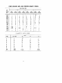
List of Tables
....................................................................................
Console Switch Functions
Console
Key Functions
........................................................................................
....................................................................................
Console Lamp Indications
............................................................................
Memory Reference
instructions
......................................................................
Group 1 Operate Microinstructions
......................................................................
Group 2 Operate Microinstructions
10
10
11
13
16
18
List of Illustrations
Typical PDP-5 Computing
System ........................................................................
..................................................................................
PDP-5 System Components
Arithmetic
and Control Element ............................................................................
................................................................................................
Operator
Console
....................................................
Bit Assignments
Memory Reference
Instruction
..........................................................................
ICT Instruction
Bit Assignments
......................................................
Group 1 Operate Instruction
Bit Assignments
........................................................
Group 2 Operate Instruction
Bit Assignments
Input-Output
Control
Element ..............................................................................
..............................................................................................
Data Break Timing
....................................................
Component
Location
and Installation
Diagram
..........................................................
Type 4605 Pulse Amplifier
Logic Diagram
V
vi
2
7
10
13
15
16
17
27
30
48
50
Figure
1 Typical
PDP-5 Computing
vi
System
CHAPTER
1
SYSTEM INTRODUCTION
The Digital Equipment Corporation
Programmed
Data Processor-5 (PDP-5)
is designed for use as a small-scale
general-purpose
computer,
an independent information handling facility in a larger computer system, or as the
control element in a complex processing system. The PDP-5 is a one-address,
fixed word length, parallel computer using 12 bit, twos complement arithmetic.
Cycle time of the 1024- or 4096-word random address magnetic-core memory is 6 microseconds.
Standard features of the system include indirect
addressing and facilities for instruction
skipping, program interruption,
or
program halting as functions of input-output device conditions.
The 6-microsecond
cycle time of the machine provides a computation rate of
55,555 additions per second. Addition is performed in 18 microseconds (with
one number in the accumulator)
and subtraction is performed in 30 microseconds (with the subtrahend in the accumulator).
Multiplication
is performed
in approximately
2.0 milliseconds
by a subroutine that operates on two 12-bit
numbers to produce a 24-bit product, leaving the 12 most significant bits in
the accumulator. Division of two 12-bit numbers is performed in approximately
3.5 milliseconds by a subroutine that produces a 12-bit quotient in the accumulator and a 12-bit remainder in core memory.
Flexible, high-capacity,
input-output
capabilities of the computer allow it to
operate a variety of peripheral equipment.
In addition to standard Teletype
and perforated-tape equipment, the system is capable of operating in conjunction with a number of optional devices such as high-speed perforated-tape
readers and punches, card equipment, a line printer, analog-to-digital
converters, cathode-ray tube displays, and magnetic-tape equipment. The system
is easily adapted for connection to equipment of special design.
PDP-5 is completely
self-contained,
requiring no special power sources or
environmental
conditions. A single source of 115volt, 60cycle, single-phase
power is required to operate the machine. Internal power supplies produce
all of the operating voltages required. Solid-state system modules and built-in
provisions. for marginal checking insure reliable operation in ambient temperatures between 50 and 105 degrees Fahrenheit.
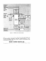
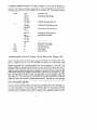
The primary functions of the PDP-5 system are performed by an arithmetic
and control element, an input-output
control element, and the input-output
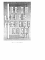
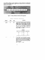
devices. Figure 2 shows the relationship of these elements.
1
Figure 2 PDP-5
System
2
Components
The arithmetic and control element contains all of the registers that perform
arithmetic and logic operations, the core memory for storage and retrieval of
data and instructions, and the operator console, which indicates the contents
of registers and provides a means of modifying data. Chapter 2 of this handbook describes these functions in detail.
The input-output control element provides communications
between the arithmetic and control element and standard, optional, or special input-output
devices. Components of this control may be housed in the main computer
cabinet or with the I/O device. I/O device selection, input-output skip, program
interrupt, input-output halt, and data break control are features of this element
and are discussed in Chapter 3.
All of the input-output devices are optional except the Teletype Model 33 ASR.
Standard and optional I/O equipment programming
information
is presented
in Chapter 4.
THE TELETYPE MODEL 33 ASR provides a means of supplying data to the
computer from perforated tape or a keyboard, or of receiving output information from the computer in the form of perforated tape or typed copy.
Maximum speed of these operations is ten characters per second.
THE HIGH SPEED PERFORATED TAPE PUNCH AND CONTROL
perforates 8-hole paper tape at a rate of 63.3 lines per second.
TYPE 75A
THE HIGH SPEED PERFORATED TAPE READER AND CONTROL TYPE 750
senses 8-hole perforated paper tape photoelectrically
at the rate of 300 lines
per second.
THE ANALOG-TO-DIGITAL CONVERTER TYPE 137 is wired into each system.
Modules to activate this feature are optional. The converter operates in the
normal successive approximation fashion, using existing computer registers as
the shift register and buffer register. The converter provides a 12-bit word;
however, the last bit is insignificant.
THE CARD READER AND CONTROL TYPE 451 operates at a rate of 200 or 800
cards per minute. Cards are read column by column. Column information
may be read in alphanumeric
or binary mode. The alphanumeric
mode converts the 12-bit Hollerith Code of one column into the 6-bit binary-coded
decimal code with code validity checking. The binary mode reads a 12-bit
column directly into the PDP-5. Approximately
one percent of a Card Reader
program running time is required to read the 80 columns of information at
the 200 cards per minute rate.
THE CARD PUNCH CONTROL TYPE 450 permits operation of a standard
IBM Type 523 Summary Punch with the PDP-5. Punching can occur at a rate
of 100 cards per minute. Cards are punched one row at a time at 40millisecond intervals.
3
THE AUTOMATIC LINE PRINTER AND CONTROL TYPE 64 prints a selection
of 63 characters at up to 300 lines of 120 characters per minute. Printing
of one group of 120 characters can be carried out while the next 120 characters are being loaded into the printer. Loading, printing, and format are under
program control. Format is program selected from a punched format tape in
the printer.
THE INCREMENTAL PLOTTER AND CONTROL TYPE 350 provides high-speed
plotting of points, continuous curves, points connected by curves, curve identification symbols, letters, and numerals under program control.
THE DATA CHANNEL MULTIPLEXER TYPE 129 automatically
transfers data
directly between the computer core memory and up to four I/O devices. The
computer core memory address of each transfer is specified by the I/O device.
Transfers are made through the normal data break facilities and breaks are
performed in accordance with an assigned I/O device priority.
THE OSCILLOSCOPE DISPLAY TYPE 34B plots data point by point on a high
resolution oscilloscope,
such as the Tektronix Model RM 503. Each axis is
determined by 10 binary bits.
THE PRECISION CRT DISPLAY TYPE 30N displays data on a 9% inch by
91/4 inch area. Information is plotted point by point to form either graphical
or tabular data. The X and Y coordinates are each controlled by a separate
lo-bit word.
THE LIGHT TYPE PEN 370 is a photoelectric device which signals the computer
when it detects information displayed on the Type 30N Precision CRT Display.
Upon signal from the light pen, the computer carries out previously programmed instructions.
THE DUAL MICRO TAPE SYSTEM TYPE 555-552
provides a fixed-address
magnetic-tape facility for high-speed loading, readout, and program updating.
A system consists of a Type 555 Micro Tape Transport and a Type 552 Micro
Tape Control. Each transport contains two independent tape drivers. Up to
four transports (8 drives) can be used with one control. Each reel, containing
up to four-million
bits of data, can be written or read under program control.
THE AUTOMATIC MAGNETIC TAPE CONTROL TYPE 57A reads and writes
high and low density, IBM compatible
magnetic tape at a transfer rate of
15,000 characters per second.
The
tion
following
special
terms
of equipment
functions
are used throughout
and instructions:
A=>B
handbook
Contents
of A
A replaces
B or B is set to A
Y
Any core memory
yi
Any given bit in Y
Yl-4
Bits 1 through
Y;
The 1 output
ister Y
N
C(A),-, = > C(Y),-,,
in the explana-
Explanation
Term
C(A)
this
Number
location
4 of Y
of bit j of reg-
N to the radix
r
The contents
of bits
6
through
11 of core memory
location Y are set to correspond with the contents of bits
0 through
5 of register
A
4L
Exclusive
OR
V
Inclusive
OR
A
AND
K
Ones complement
5
of A
CHAPTER
ARITHMETIC
AND
2
CQNTRQL
Functions
To perform the required arithmetic,
logic, and data processing operations
and to store, retrieve, control, and modify information
the arithmetic
and
control element uses the logic components shown in Figure 3 and described
in the following paragraphs.
ACCUMULATOR
(AC)
Arithmetic
operations are performed in this 12-bit register. The AC can be
cleared or complemented.
Its contents can be rotated right or left with the
link. The contents of the memory buffer register can be added to the contents
of the AC and the result left in the AC. The contents of both these registers
may be combined by the logical operation AND, the result remaining in the
AC. The memory buffer register and the AC also have gates which allow them
to be used together as the shift register and buffer register of a successive
approximation
analog-to-digital
converter. The inclusive OR may be formed
between the AC and the switch register on the operator console and the result
left in the AC.
The accumulator
mation transfers
the accumulator.
also acts as an input-output register. All programmed inforbetween core memory and an external device pass through
LINK (L)
This one-bit register is used to extend the arithmetic facilities of the accumulator. It is used as the carry register for twos complement arithmetic. This
feature greatly simplifies multiple precision arithmetic. The link can be cleared
and complemented,
and it can be rotated as part of the accumulator.
MEMORY
BUFFER
REGISTER
(MB)
All information transfers between the computer registers
ory are temporarily
held in the MB. Information can be
from the accumulator
or memory address register. The
incremented by one or two, or shifted right. Information
6
and the core memtransferred into MB
MB can be cleared,
can be set into the
MEMORY
BUFFER
REGISTER
Figure 3
Arithmetic
and Control Element
MB from an external device during a data break or from core memory, via
the sense amplifiers. Information is read from a memory location in 2 microseconds and rewritten in the same location in another 2 microseconds of one
6-microsecond memory cycle.
MEMORY
ADDRESS
REGISTER
The address in core memory which is currently
7
(MA)
selected for reading or writing
is contained in this 12-bit register. Therefore, all 4096 words of core memory
can be addressed directly by this register. The MA can be cleared or incremented by one. Data can be set into it from the memory buffer register, from
the switch register, or from an l/O device. The output can be disabled (i.e.
forced to indicate all binary zeros) without affecting the contents of the register.
INSTRUCTION
REGISTER
(IR)
This 4-bit register contains the operation code of the instruction currently
being performed by the machine. Information
is loaded into the IR from the
memory buffer register during a Fetch cycle. The contents of the three most
significant bits of the IR are decoded to produce the eight instructions,
and
affect the cycles and states entered at each step in the program. The least
significant bit (the indirect bit) is used in addressing core memory to specify
a defer cycle in addressable instructions and to differentiate the two groups
operate instructions.
PROGRAM
COUNTER
(PC)
The program sequence, that is, the order in which instructions are performed,
is determined by the PC. This 12-bit core memory register contains the address
of the core memory location from which the last instruction was taken. Information enters the PC from the MB, since core memory address 0 is used as
the PC. Because the PC is in core memory, it can be manipulated by the program in the same manner as any other core memory location.
CORE
MEMORY
The core memory provides storage for instructions to be performed and information to be processed or distributed.
This random addressable magnetic
core memory holds either 1024 or 4096 12-bit words. Memory location 0 is
used as the program counter, location 1 is used to store the contents of the PC
following a program interrupt, and location 2 is used to store the first instruction to be executed following a program interrupt. (When a program interrupt
occurs, the contents of the PC are stored in location 1; and program control is
transferred to location 2 automatically.)
Locations 10 through 17 are used for
auto-indexing. All other locations can be used to store instructions or data.
STATES,
TIMING,
CONTROL,
AND IOP GENERATOR
This logic component of the computer establishes the basic timing of all computer operations, controls the operation of all previously mentioned registers,
and generates the three IOP pulses which are supplied to the device selectors
in the input-output control element. It also establishes the cycles or primary
control states entered to accomplish each instruction. The control state entered
next is determined at the completion of the current one. All states except break
are determined by the instruction.
PROGRAM COUNTER (P):
This state reads the contents of the progr m
counter from core memory location 0 into the MB, increments the contents a of
8
the MB by 1 (or 2 for a skip instruction),
and rewrites the contents of the
MB back in location 0. The incremented contents of the PC remain in the MB
as the address of the current instruction. During a jump or jump to subroutine
instruction, the effective address specified by the jmp or jms is written into
location 0 to transfer program control. Completion of a P cycle initiates a
Fetch cycle.
FETCH (F):
ory location
During this state an instruction word is read from the core memspecified by the contents of the program counter.
EXECUTE 1 (E,): This state occurs for all instructions requiring an operand
from core memory. The contents of the core memory location specified by the
least significant bits of the instruction are read into the memory buffer register
and the operation specified by bits 0 through 2 of the instruction is performed.
EXECUTE 2 (E2): When a jump to subroutine instruction is being executed,
this state is entered to write the contents of the program counter into core
memory location Y.
DEFER (D): When a 1 is present in bit 3 of a memory reference instruction,
the defer state is entered to obtain the full 12-bit address of the operand from
the address in the current page or page 0 specified by bits 4 through 11 of
the instruction. The process of address deferring is called indirect addressing
because access to the operand is addressed indirectly, or deferred, to another
memory location.
BREAK (B):
When this state is established, the sequence of instructions
is
broken for a data interrupt, The break normally occurs at the completion of the
current instruction.
If the interrupt occurs during a jump or jump to subroutine instruction,
the break begins only after two instructions
have been
completed (the instruction jumped to is executed). The data interrupt allows
information
to be transferred directly between core memory and an external
device. When this transfer has been completed, the program sequence is
resumed from the point of the break.
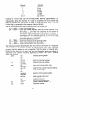
OPERATOR
CONSOLE
Switches and keys on the operator console allow manual program and
information
insertion or modification.
Indicator lamps display the status of
the machine and the contents of major registers. Register indicators light
to denote the presence of a 1 in a specific bit. While a program is running,
the brightness of an indicator is related to the percentage of time that the
related bit holds a 1.
Figure 4 shows the operator console and the following
of switches, keys, and indicators.
9
tables list the function
Figure
4
CONSOLE
Operator
SWITCH
Console
FUNCTIONS
Switch
Function
SWITCH
REGISTER
Provides a means of manually setting a 12.bit word
into the machine.
Switches
in the up position correspond
to ones, down, to zeros. Contents
of this
register are loaded into the memory address register by the LOAD ADDRESS key, or into the memory
buffer register
and core memory
by the DEPOSIT
key. The contents
of the switch register
(SR) can
be set into the accumulator
under program control.
SINGLE
STEP
Causes the computer
to halt at the completion
of
each memory
cycle. Repeated
operation
of the
CONTINUE
key steps the program
one cycle at a
time so that the state of the machine
can be examined at each step.
SINGLE
INST
Causes the computer
each instruction.
POWER
Controls
CONSOLE
primary
KEY
Key
LOAD
ADDRESS
to stop
power
at the completion
of
in the computer.
FUNCTIONS
Functions
Deposits
the contents
of the
the memory address register.
10
switch
register
into
CONSOLE
KEY FUNCTIONS
(continued)
Functions
Key
START
Starts the computer
after turning
off the program
interrupt
system and clearing
both the AC and L.
The first instruction
is taken from the core memory at the address
presently
in the memory
address register.
DEPOSIT
Sets the word contained
in the switch register into
the core memory
at the location
specified
by the
memory
address
register.
The results
remain
in
the memory
buffer register.
The memory
address
register is then incremented
by one, allowing
rapid
data deposits
in sequential
core memory locations.
EXAMINE
Sets the contents
of the core memory
location selected by the memory
address
register
into the
accumulator
and the memory
buffer register.
The
memory
address
register
is then incremented
by
one, allowing
rapid examination
of data in sequential core memory locations.
STOP
Causes the computer
to stop at the completion
of
the memory
cycle in progress
at the time of key
operation.
CONTINUE
Causes the computer
to resume execution
of the
instruction
at the address held in the PC, from the
program
state indicated
by the panel lamps.
LOCK
Disables all console keys and switches
except the
SR to prevent
inadvertent
power turn-off
or program interference
while a program
is in progress.
SWITCH
CONSOLE
LAMP INDICATIONS
Indications
Lamp(s)
MEMORY
ADDRESS
Indicate
the contents
of the memory
MEMORY
BUFFER
indicate
the contents
of the memory
ACCUMULATOR
Indicate
the contents
of the accumulator.
INSTRUCTION
Indicate
the contents
of the instruction
RUN
Indicates
that the computer
11
address
register.
buffer
register.
is executing
register.
instructions.
CONSOLE
LAMP INDICATIONS
(continued)
Law(s)
IN-OUT
Indications
HALT
Indicates that the computer
is waiting
output device to complete its operation.
LINK
Indicates
PROGRAM
EXECUTE,
SINGLE
COUNTER,
FETCH,
DEFER, BREAK
STEP and SINGLE
the contents
of the carry
for an input-
link.
Indicate the primary
control
state of the machine
and that the next memory cycle will be a program
counter,
fetch,
execute,
defer,
or break
cycle
respectively.
INST
POWER
Indicate
that the SINGLE STEP
switch is on the ON position.
Indicates
that
power
is turned
or SINGLE
INST
on in the computer.
Instructions
Instruction words are of two types: memory reference and augmented. Memory
reference instructions
store or retrieve data from core memory, while augmented instructions do not. All instructions utilize bits 0 through 2 to specify
the operation code. Operation codes of 0, through 5* specify memory reference instructions,
and codes of 6, and 7, specify augmented instructions.
Instruction
execution times are multiples
of the 6-microsecond
computer
cycle time. Memory
reference
instructions
require
12, 18, or 24 microseconds
for execution. Indirect addressing increases the execution time of a memory
reference instruction by 6 microseconds. The augmented instructions,
inputoutput transfer and operate, are performed in 12 microseconds.
MEMORY
Word format
instructions
of memory
are
explained
REFERENCE
reference
in the
Since this system can contain
address
all locations.
To simplify
INSTRUCTIONS
instructions
Memory
a 4096-word
addressing,
is shown in Figure 5, and the
Reference
Instructions
memory,
the
memory
Table.
12 bits are required to
is divided
into blocks,
or pages, of 128 words (200, addresses). Pages are numbered 0, through
37*, a 1024-word memory having pages 0, through 7*, and a 4096-word
memory using all 32 pages. The seven address bits (bits 5 through 11) of
a memory reference instruction
can address any location in the page on
which the current instruction is located by placing a 1 in bit 4 of the instruction. By placing a 0 in bit 4 of the instruction, any location in page 0 can be
addressed directly from any page of core memory. All other core memory
locations must be addressed indirectly by placing a 1 in bit 3 and placing a
12
7-bit effective
address
location
in the current
address
of the operand.
Figure
5
in bits 5 through
11 of the instruction
page or page 0, which contains
the full
Memory
Reference
MEMORY
Mnemonic
Symbol
and Y
Instruction
REFERENCE
Octal
Code
Time
b*sec)
0
18
to specify
the
12-bit absolute
Bit Assignments
INSTRUCTIONS
Operation
Logical AND. The AND operation
is performed
between the C(Y) and the C(AC). The result
is left in the AC, and the original
C(AC) are
lost. The C(Y) are unchanged.
Corresponding
bits are compared
independently.
This instruction,
often called extract
or mask, can
be considered
as a bit-by-bit
multiplication.
C(Y),/\ C(AC)i =>
C(AC)i
Example
C(AC)i
original
0
0
1
tad Y
1
18
c(y>i
0
1
0
C(AC)i
final
0
0
0
Twos complement
add. The C(Y) are added
to the C(AC) in twos complement
arithmetic.
The result is left in the AC and the original
C(AC) are lost. The C(Y) are unchanged.
If
there is a carry from AC,,, the link is complemented. This feature is useful in multiple precision arithmetic.
C(Y) + C(AC) = > C(AC).
13
MEMORY
Mnemonic
Symbol
REFERENCE
Operation
Code
INSTRUCTIONS
(continued)
Time
(usec)
Operation
is2 Y
2
18
Index and skip if zero. The C(Y) are incremented
by one in twos complement
arithmetic.
If the resultant
C(Y) = 0, the next
instruction
is skipped.
If the resultant
C(Y) # 0, the program
proceeds to the next
instruction.
The C(AC) are unaffected.
C(Y) + 1 = > C(Y) .
if result = 0, C(PC) + 1 = > C(PC).
dca Y
3
18
Deposit and clear AC. The C(AC) are deposited
in core memory location Y and the AC is then
cleared. The previous C(Y) are lost.
C(AC) = > C(Y), then 0 = > C(AC).
jms Y
4
24
Jump to subroutine.
core memory location
memory
location
Y.
taken from location Y
C(PC) + 1 = > C(Y)
Y + 1 = > C(PC>
imp Y
5
12
Jump
to Y. The C(PC)
contained
in core
memory location 0 are set to address Y. The
next instruction
is taken from core memory
location Y. The original C(PC) are lost.
Y =>
C(PC).
The C(PC) contained
in
0 are deposited
in core
The next instruction
is
+ 1.
-
AUGMENTED
INSTRUCTIONS
There are two augmented
instructions
or instructions
which
do not reference
core memory.
They
are the input-output
transfer,
which
has an operation
code of 6, and the operate,
which
has an operation
code of 7. Bits 3 through
11 within
these
instructions
function
as an extension
of the operation
code
and can be microprogrammed
to perform
tion.
are
Augmented
instructions
several operations
two-cycle
(P,
with one instruc-
F) instructions
requiring
12
microseconds for execution. During the second cycle, three clock pulses are
available to initiate operations as a function of bit microprogramming.
These
clock pulses are designated event times 1, 2 and 3 and are separated by 1
microsecond.
INPUT-OUTPUT
output transfer
metic
control
and
TRANSFER INSTRUCTION:
Microinstructions
of the input(iot) instruction effect information transfers between the arith-
control
element.
element
Specifically,
and
an
input-output
when operation
14
device
via
the
input-output
code 6 is detected,
the IOP
generator is enabled to produce IOP 1, 2, and 4 pulses as a function of the
contents of bits 9 through 11. These pulses are gated in the device selector
of the selected I/O device to produce the IOT pulses which enact a transfer.
The format of the iot instruction is shown in Figure 6. Bits 3 through 8 are
used to select the I/O device; and bits 9 through 11 enable generation of IOP
pulses during event times 3, 2, and 1, respectively. Operations performed by
iot microinstructions
are explained in Chapter 4.
Figure 6
IOT Instruction Bit Assignments
OPERATE INSTRUCTION:
The operate instruction consists of two groups of
microinstructions.
Group 1 (opr 1) is principally for clear, complement, rotate,
and increment operations and is designated by the presence of a 0 in bit 3.
Group 2 (opr 2) is used principally in checking the contents of the accumulator and link and continuing to or skipping the next instruction based on the
check. A 1 in bit 3 designates an opr 2 microinstruction.
Group 1 operate microinstruction
format is shown in Figure 7, and the microinstructions are listed in the table below. Any logical combination of bits within
this group can be combined into one microinstruction.
For example, it is possible to assign ones to bits 5, 6,and 11; but it is not logical to assign ones to
bits 8 and 9 simultaneously
since they specify conflicting operations. If ral or
rar is specified, neither cma or cml may be specified, and conversely. If rtl or
rtr is specified, neither cma, cml, or iac may be specified, and conversely.
15
Figure
Mnemonic
Symbol
7
Group
1 Operate
GROUP
1 OPERATE
Octal
Code
Event
Time
Instruction
Bit Assignments
MICROINSTRUCTIONS
Operation
cla
7200
1
Clear AC. To be used alone
binations.
0 = > C(AC).
CII
7100
1
Clear L.
0 =>
C(L).
cma
7040
2
Complement
AC. The C(AC)
ones complement
of C(AC).
C(m)
=>
C(AC).
cml
7020
2
Complement
L.
C(L) = > C(L).
rar
7010
2
Rotate AC and L right. The C(AC)
C(L) are rotated right one place.
C(AC)i =>
C(AC)i+,
WC),,
=>
C(L)
C(L) = > COW,
ral
7004
2
Rotate AC and L left. The C(AC)
are rotated left one place.
C(AC)i = > C(AC)im,
WC),
= > C(L)
C(L) = > WC),,
and the C(L)
rtr
7012
2.3
Rotate two places to the right.
two successive
rar operations.
Equivalent
16
or in opr 1 com-
are
set to the
and
the
+o
GROUP
Mnemonic
Symbol
1 OPERATE
Octal
Code
MICROINSTRUCTIONS
Event
Time
(continued)
Operation
ral
7004
2
Rotate AC and L left. The C(AC)
are rotated left one place.
C(AC)i =>
C(AC)i-1
WC),
= > C(L)
C(L) =>
WC),,
and the C(L)
rtr
7012
2,3
Rotate two places to the right.
two successive
rar operations.
Equivalent
to
rtl
7006
23
Rotate two places to the left.
two successive
ral operations.
Equivalent
to
iac
7001
3
Index AC. The C(AC) are incremented
in twos complement
arithmetic.
C(AC) +l =>
C(AC).
by one
w
7000
-
No operation.
delay.
Causes
a 12Psec
program
Group 2 operate microinstruction
format is shown in Figure 8 and the microinstructions are listed in the table below. Any logical combination of bits within
this group can be composed in one microinstruction.
If skips are combined in a single instruction, the inclusive OR of the conditions determines the skip. For example, if ones are designated in bits 6 and 7
(sza and snl), the next instruction is skipped if either C(AC) = 0, or C(L) = 1,
or both. The cla microinstruction
from group 1 can be combined with group 2
commands. This command occurs at event time 2 with respect to the event
times listed in the following table.
Figure
8
Group
2 Operate
Instruction
17
Bit Assignments
GROUP
Mnemonic
Symbol
Octal
Code
2 OPERATE
MICROINSTRUCTIONS
Event
Time
Operation
cla
7600
2
Clear AC. To be used alone
binations.
0 = > C(AC)
spa
7510
1
Skip on positive AC. If the C(AC) is a positive
number,
the next instruction
is skipped.
If C(AC), = 0, then C(PC) + 1 =>
C(PC)
sma
7500
1
Skip on minus AC. If the C(AC) is a negative
number, the next instruction
is skipped.
If C(AC), = 1, then C(PC) + 1 =>
C(PC)
sna
7450
1
Skip on non-zero AC.
If C(AC) # 0, then C(PC)
sza
7440
1
Skip on zero AC.
If C(AC) = 0, the C(PC)
or in opr 2 com-
+ 1 = > C(PC)
+ 1 = > C(PC)
SZI
7430
1
Skip on zero L. If C(L) = 0, the next instruction is skipped.
If C(L) = 0, the C(PC) + 1 =>
C(PC)
snl
7420
1
Skip on non-zero L.
If C(L) = 1, then C(PC)
+
1 =>
next
C(PC)
sb
7410
1
Skip, unconditional.
The
skipped.
C(PC) + 1 =>
C(PC)
instruction
is
osr
7404
3
OR with switch register.
C(SR) V C(AC) = > C(AC)
hlt
7402
3
Halt. Stops the program.
If this instruction
is
combined
with others in the opr 2 group, the
computer
stops immediately
after completion
of the cycle in process.
Programming
MEMORY
The
terms
following
ADDRESSING
are used in memory
address
Definition
Term
Page
programming:
A block of 128
addresses).
18
core memory
locations
(200,
Definition
Term
Page
The page containing
the instruction
being
executed;
as determined
by bits 0 through
5
of the program counter.
Page Address
An 8-bit number contained
in bits 4 through
11 of an instruction
which designates
one of
256 core memory
locations.
Bit 4 of a page
address
indicates
that the location
is in(the
current
page when a 1, or indicates
it is in)
page 0 when a 0. Bits 5 through
11 designate
one of the 128 locations
in the page determined by bit 4.
Absolute
Address
A 12-bit number
in core memory.
Effective
Address
The address of the operand. When the address
of the operand
is in the current
page or in
page 0, the effective
address
is a page address. Otherwise,
the effective
address is an
absolute
address stored in the current
page
or page 0 and obtained by indirect addressing.
Current
Organization
Total
Total
of the
locations
addresses
core
memory
is summarized
(decimal)
(octal)
Number of pages
Page designations
(decimal)
(octal)
Number of locations per page (decimal)
Addresses
within a page (octal)
Four methods
of obtaining
binations
of bits 3 and 4.
the
effective
used to address
any location
as follows:
1024
o-1777
4096
o-7777
8
o-7
32
o-37
128
o-177
128
o-177
address
are
used
Effective
as specified
by com-
Address
Bit 3
Bit 4
0
0
0
1
1
0
The absolute
address of the operand is taken
from the contents
of the location in page 0
designated
by bits 5 through
11.
1
1
The absolute address of the operand is taken
from the contents
of the location in the current page designated
by bits 5 through
11.
The operand
is in page 0 at the address
specified by bits 5 through
11.
The operand
is in the current
page at the
address specified
by bits 5 through
11.
19
The following
example
indicates
in core memory.
Suppose
it is
C, and D to the contents
of the
page 2. The instructions
in this
tents of bit 4, the contents
of
take the following
form:
Location
Page 0
Contents
the use of bits 3 and 4 to address
any location
desired
to add the contents
of locations
A, B,
accumulator
by means of a routine
stored
in
example
indicate
the operation
code, the conbit 3, and a 7-bit address.
This routine
would
Page
Page 1
Location
Contents
Location
2
Contents
Remarks
R
tad 00 A
Direct to data in
we
0
s
tad 01 B
Direct to data in
same page
T
tad 10 M
Indirect
specified
to address
in page 0
U
tad 11 N
Indirect
specified
to address
in same page
.
.
.
.
A
M
xxxx
C
C
D
xxxx
xxxx
B
N
xxxx
D
Routines,
using
128 instructions
or less, can be written
in one page using
direct
addresses
for looping
and using
indirect
addresses
for data
stored
in other
pages.
When planning
the location
of instructions
and data in core
memory,
remember
that
the following
locations
are reserved
for special
purposes:
Purpose
Address
0,
Is the program
18
Stores the contents
following
a program
2,
Stores the first instruction
following
a program interrupt.
10, through
INDIRECT
part (bits
17,
counter.
of the program
interrupt.
to
counter
be executed
Auto-indexing.
ADDRESSING:
When
indirect
addressing
is specified,
the address
5-11) of a memory
reference
instruction
is interpreted
as the address
20
of a location containing not the operand, but the address of the operand. Consider the instruction tad A. Normally, A is interpreted as the address of the
location containing the quantity to be added to the AC. Thus, if location 100
contains the number 5432, the instruction tad 100 causes the quantity 5432
to be added to the AC. Now suppose that location 5432 contains the number
6543. The instruction tad i 100 (where i signifies indirect addressing) causes
the computer to take the number 5432, which is in location 100, as the effective address of the instruction and the number in location 5432 as the operand.
Hence, this instruction results in the quantity 6543 being added to the contents
of the AC.
AUTO-INDEXING: When a location between 10, and 17, in page 0 is specified
as the address in an instruction, and bit 3 is a 1, the contents of that location
are read, incremented by one rewritten in the same location, and then taken as
the effective address of the instruction. This feature is called auto-indexing.
If location 12, contains the number 5432 and the instruction dca i 12 is given,
the contents of the accumulator are deposited in core memory location 5433,
and the number 5433 is stored in location 12.
STALING
AND LOADING
Data is stored in any core memory location by use of the dca Y instruction.
This instruction clears the AC to simplify loading of the next datum. If the data
deposited is required in the AC for the next program operation, the dca must
be followed by a tad Y for the same address.
All loading of core memory information into the AC is accomplished by means
of the tad Y instructions,
preceded by an instruction that clears the AC such
as cla or dca.
Transfer of program control to any core memory location uses the jmp or jms
instructions.
The jmp i (indirect address, 1 in bit 3) is used to address any
location in core memory which is not in the current page or page 0.
The jms Y is used to enter a subroutine which starts at location Y+ 1. The
C(PC) + 1 => C(Y) and Y + 1 = > C(PC). To exit a subroutine the last
instruction is a jmp i Y, which returns a program control to C(Y).
Since the program counter is in core memory location 0, the program flow can
be altered by depositing some number in location 0. If the number X is deposited in 0, the next instruction is taken from location X+1.
INDEXING
OPERATIONS
The isz instruction
is used to count repetitive program operations without
disturbing the contents of the accumulator. Counting is performed by storing
a twos complement negative number equal to the number of program loops to
be counted. Each time the operation is performed, the isz instruction is used to
21
increment the contents of this stored number and check the result. When the
stored number becomes zero, C(Y) = 0, the specified number of operations
have occurred and the program skips out of the loop and back to the
main sequence.
This instruction
is also used for other routines
in which
the contents
of a
memory location are incremented
without disturbing
the contents of the
accumulator,
such as storing information
from an I/O device in sequential
memory locations or using core memory locations to count I/O device events.
LOGIC
OPERATIONS
The PDP-5 instruction
list includes the logic instruction,
and Y. From this
instruction short routines can be written to perform the inclusive and exclusive
OR operations.
LOGIC AND: The logic AND operation between the contents of the Accumulator
and the contents of a core memory location Y is performed directly by means
of the and Y instruction.
INCLUSIVE OR: Assuming value A is in the AC and value B is stored in a known
core memory address, the following sequence performs the inclusive OR. The
sequence is stated as a utility subroutine called ior.
{calling sequence
I
/enter
with argument
ior,
teml,
tem2,
jms ior
in AC; exit with logical
(address
(return)
result in AC
of B)
0
dca tern 1
tad i ior
dca tern2
tad i tern2
cma
and tern1
tad i tern2
is2 ior
jmp i ior
0
0
EXCLUSIVE OR: The exclusive OR operation for two numbers, A and B, can be
performed by a subroutine called by the mnemonic code xor. In the following
general purpose xor subroutine, the value A is assumed to be in the AC, and
the address of the value B is assumed to be stored in a known core memory
location.
22
/calling
:
/enter
sequence
with argument
in AC; exit with logical
xor,
0
dca tern1
tad i xor
dca tern2
tad tern1
and i tern2
cma V iac
cl1 V ral
tad tern1
tad i tern2
is2 xor
jmp i xor
teml,
0
tem2,
0
jms xor
(address
(return)
result in AC
of B)
An xor subroutine can be written using fewer core memory locations by making
use of the ior subroutine; however, such a subroutine requires longer to execute.
A faster xor subroutine can be written by storing the value E? in the second
instruction of the calling sequence instead of the address of B; however, the
resulting subroutine is not as utilitarian as the routine given here.
ARITHMETIC
OPERATIONS
One arithmetic instruction is included in the PDP-5 order code, the twos complement add: tad Y. Using this instruction,
routines can easily be written to
perform addition, subtraction,
multiplication,
and division in twos complement arithmetic.
TWOS COMPLEMENT ARITHMETIC:
In twos complement arithmetic, addition,
subtraction,
multiplication,
and division of binary numbers is performed in
accordance with the common rules of binary arithmetic. In PDP-5, as in other
machines utilizing complementation
techniques, negative numbers are represented as the complement of positive numbers, and subtraction is achieved
by complement
addition. Representation of negative values in ones complement arithmetic is slightly different from that in twos complement arithmetic.
The ones complement of a number is the complement of the absolute positive
value; that is, all ones are replaced by zeros and all zeros are replaced by ones.
The twos complement of a number is equal to the ones complement
of the
positive value plus one.
In ones complement arithmetic a carry from the sign bit (most significant bit)
is added to the least significant bit in an end-around carry. In twos complement
arithmetic a carry from the sign bit complements the link (a carry would set
23
the link to one if it were properly
no end-around carry.
cleared before the operation),
and there is
A ones complement
representation
of a negative number is always one less
than the twos complement
representation of the same number. Differences
between ones and twos complement
representations
are indicated in the
following list.
Number
+5
+4
+3
+2
+1
+o
-0
-1
-2
-3
-4
-5
1s Comolement
2s Complement
000000000101
000000000100
000000000011
000000000010
000000000001
000000000000
111111111111
111111111110
111111111101
111111111100
111111111011
111111111010
000000000101
000000000100
000000000011
000000000010
000000000001
000000000000
Nonexistent
111111111111
111111111110
111111111101
111111111100
111111111011
Note that in twos complement there is only one representation
which has the value zero, while in ones complement there are
tions. Note also that complementation
does not interfere with
either ones complement or twos complement arithmetic; bit 0
positive numbers and a 1 for negative numbers.
for the number
two representasign notation in
remains a 0 for
To form the twos complement of any number in the PDP-5, the ones complement is formed, and the result is incremented by one. This is accomplished by
the instruction
cma combined with an iac instruction.
Since both of these
instructions
are functions of the opr 1 instruction and the actions occur at
different event times, they can be combined to form:
cia -
7041 -
2, 3
Complement and index AC
ADDITION: The addition of a number contained in a core memory location and
the number contained in the accumulator is performed directly by using the
tad Y instruction, assuming that the binary point is in the same position and
that both numbers are properly represented in twos complement
arithmetic.
Addition can be performed without regard for the sign of either the augend or
the addend. Overflow is possible, in which case the result will have an incorrect
sign, although the 11 least significant bits will be correct.
SUBTRACTION:
Subtraction
is performed by complementing
the subtrahend
and adding the minuend. As in addition, if both numbers are represented by
their twos complement,
subtraction can be performed without regard for the
signs of either number. Assuming that both numbers are stored in core
memory, a routine to find the value of A-B follows:
24
cla
tad B
cia
tad A
/Load subtrahend
into AC
/Complement
and increment
/C(AC) = A - B
25
B (cma V iac)
CHAPTER
INPUT-OUTPUT
3
CONTROL
Functions
Selected input-output devices are controlled by iot (in-out transfer) instructions.
The iot instruction is microprogrammed
to allow one basic instruction to handle
many devices (by changing the bits of the command). The command pulses
occur at various times to allow flags to be sampled (and an instruction skipped),
buffers to be cleared, and data to be transmitted to or from the accumulator.
Operational circuits of the input-output control element are shown in Figure 9.
DEVICE
SELECTOR
(DS)
Input-output equipment connected into the system is controlled by various
Device Selector pulses. These pulses:
a. Sample Device flag conditions which are fed into the input-output skip
facility.
b. Reset external register.
write information into external registers from the AC output.
dc: Read information from external register into the AC.
e. Control the I/O device.
f. Halt the computer until the external device has finished its operation.
The iot instruction causes the arithmetic and control element to produce IOP
pulses based on the contents of bits 9 through 11 of the instruction. These
pulses are designated IOP 4, 2, and 1, respectively, and occur at l-microsecond
intervals, which are identified as event times. Binary ones in the instruction
word cause the IOP pulses to be generated as follows:
Instruction
Bit
11
10
9
IOP
IOT
Pulse
Pulse
Event
Time
IOP 1
IOP 2
IOP 4
IOT 1
IOT 2
IOT 4
1
2
3
Computer
Cycle Time
T4
T5
T6
A device selector module exists for each I/O device or external register to be
addressed separately. The DS is a gating element which receives both the 1
and 0 information from bits 3 through 8 of an instruction (MB,& and the IOP
26
Figure 9
Input-Output Control Element
pulses. Each DS is wired to pass IOP pulses to a specific I/O device only when
the I/O device selection bits are set to the code which specifies operation of
the associated I/O device. The gated IOP pulses at the output of a DS are
called IOT pulses and can be used to set or reset control flip-flops, gate
information into the AC from external registers, gate information into external
registers from the AC, or skip instructions.
27
ACCUMULATOR
INPUT
Capacitor-diode
gates are provided at the inputs to the accumulator to allow
gated information to be written into the PDP-5 from several sources. Information levels from 12 separate bits of an external register can be simultaneously
set into the AC by an IOT pulse. The AC must be clear at the time information
is written in. Information pulses supplied to the AC input bus must drive it to
ground potential to write a 1 in an accumulator bit.
ACCUMULATOR
OUTPUT
A static level is available at an output bus from each bit of the accumulator.
These static levels are ground potential for a binary 1 and -3 volts for a binary
0. Data supplied to an external register is strobed into it by means of IOT pulses.
INPUT-OUTPUT
SK!P (10s)
The IOS facility allows the program to skip (or branch) according to the condition of various external devices. An IOT pulse is used to strobe the external
device, such as a flag, and sample its state. If the gating of the Device flag and
IOT pulse drives the IOS bus to ground, the instruction following the iot instruction which issued the strobe is skipped. If the input is a -3 volt potential, the
program sequence is not altered.
PROGRAM
PNTERRUPT
The program interrupt feature allows certain external conditions to interrupt
the computer program. It is used to speed the information processing of inputoutput devices or to allow certain alarms to halt the program in progress and
initiate another routine. When a program interrupt request is made, the computer completes execution of the instruction in progress before entering the
interrupt mode. A program interrupt is similar to a jms to location 1; that is,
the contents of the program counter are stored in location 1, and the program
resumes operation in location 2. The interrupt program commencing in location
2 is responsible for finding the signal causing the interruption, for removing
the condition, and for returning to the original program. Exit from the interrupt
program, back to the original program, can be accomplished
by a jmp i 1
instruction.
INPUT-OUTPUT
HALT
(IOH)
The input-output halt facility allows the computer to be halted during the time
that external devices are operating and then restarted by a pulse from the
device. The IOH state occurs when Type 137 Analog-to-Digital
Converter is
operating and may be wired to occur during the operation time of any other
device.
A specific iot instruction initiates operation of an I/O device. The I/O device
supplies an l/O-Halt pulse to the IOH that inhibits program advance. When the
I/O device completes the programmed operation, it produces a Restart pulse
28
which is received by the IOH to clear the IOH mode and to allow program
advance to the next instruction.
DATA
BREAK
This facility allows transmission
of data directly between an external device
and core memory, via the memory buffer register. During a data break, the
program is halted but the contents of the accumulator,
instruction
register,
and program counter are not disturbed. Therefore, when a data transfer is
complete, the program resumes from exactly the same condition which existed
before the break.
Data breaks require receipt of three control signals: Break Request, Transfer
Direction, and Increment Request. When a Break Request signal is received
from an I/O device, the computer completes execution of the instruction
in
progress and then enters the data break mode. If a jmp or jms instruction is in
progress when the request is received, the current instruction is completed,
and the next instruction is performed before the break is instituted. The direction of transfer and the core memory address of each transferred word are
specified by the I/O device when the break request is made. The Transfer
Direction signal controls the read or write cycle of the computer, and the
address is set directly into the memory address register. Data transfer then
takes place between the memory buffer register and the I/O device. When the
transfer is completed, the I/O device signals the computer to leave the break
mode by removing the Break Request. If additional transfers are to occur, a
new address must be specified to the memory address register or an Increment
Request signal must be supplied to transfer data at sequential core memory
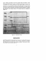
location. Figure 10 indicates the timing of these signals. The levels of these
signals are:
Signa!
Break Request
Transfer Direction
Increment Request
Address
Data
-3 Volts
No request
Data into PDP-5
Request increment
0
0
0 Volts
Request Break
Data out of PDP-5
No request
1
1
Break Request, Transfer Direction, and Address Information signals should be
supplied simultaneously
for the first transfer. When the computer enters the
data break mode, it supplies an Address Accepted pulse to the I/O device.
When the direction of transfer is into the PDP-5 from the device, data must
be supplied to the memory buffer register input no later than 1 microsecond
after the Address Accepted pulse occurs and must be present for more than
2 microseconds, To discontinue the data break mode, the Break Request signal
must be removed no later than 4 microseconds after the address accepted
pulse occurs, or the computer will enter another cycle in the data break mode.
The Transfer Direction signal must be present when the break request is made
and cannot be changed until 4 microseconds after the Address Accepted pulse
29
occurs. Address information must also be present when the request is made,
but can be changed any time after the address is accepted. To transfer data
at sequential core memory locations the first transfer address must be supplied to the memory address register by the I/O device, and successive
addresses can be specified by the Increment Request signal. This signal cannot
occur before 1 microsecond after the address is accepted for the first transfer
and must be present no later than 4 microseconds after the address is accepted.
The maximum
and minimum
limits of this signal timing are indicated in
Figure 10.
Figure
10
Data
Break
Timing
Instructions
Two types of instructions are associated directly with the input-output controls:
those concerning the input-output
skip and those concerning the program
interrupt. The skip instructions are listed in Chapter 4 of this handbook with
the instructions for the device whose status is checked. There are two instructions for the program interrupt. They are:
30
ion -
6001
iof -
6002
-Turn
interrupt
on and enable the computer
to respond
to an
interrupt
request.
When this instruction
is given, the computer
executes
the next instruction,
then enables the interrupt.
The
additional
instruction
allows exit from the interrupt
subroutine
before allowing another interrupt
to occur.
- Turn interrupt
off i.e. disable the interrupt.
Programming
When
an interrupt
request
is acknowledged,
the interrupt
is automatically
disabled
by the program
interrupt
circuits
(not
by instructions).
The next
instruction
is taken
from
core memory
location
2. Usually
the instruction
stored
in location
2 is a imp, which transfers
program
control
to a subroutine,
which services
the interrupt..At
some time during
this subroutine
an ion instruction must be given. The ion can be given at the end of the subroutine
to allow
other interrupts
to be serviced
after program
control
is transferred
back to the
original
program.
In this application,
the ion instruction
immediately
precedes
the last instruction
in the routine.
A delay of one instruction
(regardless
of
length)
is inherent
in the ion instruction
to allow transfer
of program
control
back to the original
program
before
enabling
the interrupt.
Usually
exit from
the subroutine
is accomplished
by a jmp i 1 instruction.
The ion can be given during
the subroutine
as soon as it has determined
the
I/O device
causing
the interrupt.
This latter
method
allows
the subroutine,
which
is handling
a low priority
interrupt,
to be interrupted,
possibly
by a high
priority
device.
Programming
of an interrupt
subroutine,
which
checks
for
priority
and allows
itself to be interrupted,
must make provisions
to relocate
the contents
of the program
counter
stored in location
1; so that if interrupted,
the contents
of the PC during
the subroutine
are stored
in location
1, and the
contents
of the PC during
the original
program
are not lost.
31
CHAPTER
4
INPUT-OUTPUT
DEVICES
Use of the standard and optional equipment in a PDP-5 system is discussed
in this section. The Teletype equipment is the only standard I/O device supplied with PDP-5. All other equipment is purchased at the option of the customer to compose a system tailored to his computing needs.
Teletype
Model
33 ASR
The standard Teletype Model 33 ASR (automatic send-receive) can be used
to type in or print out information at a rate of up to ten characters per second,
or to read in or punch out perforated paper tape at a ten characters per second
rate. Signals transferred between the 33 ASR and the keyboard printer control
logic are standard serial, 11 unit code Teletype signals. The signals consist of
marks and spaces which correspond to idle and bias current in the Teletype
and zeros and ones in the control and computer. The start mark and subsequent eight character bits are one unit of time duration and are followed
by the stop mark which is two units. Appendix 2 lists the character code for
the Teletype. Punched tape format is as follows:
Tape Channel
Binary Code
(Punch = 1)
Octal Code
87
654
S
321
lo
2
110
100
6
4
Toggle switches on the right side of the Teletype console control primary power
and allow the 33 ASR to communicate with the computer in on line operation
or to prepare tapes, etc., without disturbing the computer program in local
operations. Separate pushbutton switches on the punch are used to control
power, release the mechanism to allow insertion and removal of tape, and allow
backspacing to correct errors. A three position switch on the reader advances
the tape, stops the tape, or allows free wheeling of the mechanism for tape
insertion and removal.
KEYBOARD/READER
The keyboard and tape reader control contains an 8-bit buffer (LUI) which
assembles and holds the code for the last character struck on the keyboard
32
or read from the tape. The
has been assembled and
flag is a 1, a relay contact
to the computer program
by command. Instructions
the Teletype are:
ksr kcc krs -
6031 6032 6034 -
krb -
6036
Keyboard flag becomes a 1 to signify that a character
is ready for transfer to the accumulator. When the
opens to disable the reader. This flag is connected
interrupt and input-output skip facility. It is cleared
for use in supplying data to the computer from
Skip if Keyboard flag is a 1.
Clear AC and clear Keyboard flag.
Read keyboard buffer static. (This is a static command in that
neither the AC nor the Keyboard flag is cleared.)
C(LUI) V C(AC),-, , = > C(AC),+,
Clear AC, clear Keyboard flag, and read the contents of the
keyboard buffer into C(AC),-, , .
-
A program sequence loop to look for a Teletype
character can be written as follows:
200
6031
5200
6036
201
202
look,
keyboard
or tape
ksf
/skip when LUI is full
jmp look
krb
/read LUI into AC
reader
TELEPRINTER/PUNCH
The teleprinter and tape punch control contains an 8-bit buffer (LUO) which
receives a character to be printed and/or punched from AC bits 4 through 11.
The LUO receives the 8-bit code from the AC in parallel and transmits it to
the teleprinter and tape punch serially. When the last bit has been transmitted,
the Teleprinter flag is set to 1. This flag is connected to the computer program
interrupt and input-output skip facility. It is cleared by programmed command.
The instruction list for printing or punching is:
tsf - 6041 - Skip if Teleprinter flag is a 1.
tcf
-
6042
-
Clear Teleprinter
flag.
tpc -
6044 -
Load the LUO from the C(AC),-,, and print and/or punch the
character.
tls -
6046 -
Load the LUO from the C(AC),_,,,
and print and/or punch the character.
A program sequence loop to print and/or
is free can be written as follows:
free,
tsf
jmp free
tls
Tape
clear
the
punch a character
/skip
when
/load
LUO, print
Teleprinter
flag,
when the LUO
free
High Speed Perforated
Reader and Control Type
or punch
750
This device senses 8-hole perforated paper or Mylar tape photoelectrically
at 300 characters per second. The reader control requests reader movement,
transfers data from the reader into the reader buffer (RB), and signals the
33
computer
when
incoming
data is present.
Reader
tape movement
is started
by a reader
control
request
to simultaneously
release
the brake and engage
the clutch.
The 8-bit reader
buffer
sets the Reader
flag to 1 when it has been
filled from the reader
and transfers
data into bits 4 through
11 of the accumulator
under
computer
command.
The Reader
flag
is connected
to the
computer
program
interrupt
and input-output
skip facility.
It is cleared
by IOT
pulses. Computer
instructions
for the reader are:
rsf rrb -
6011
6012
-
rfc
6014
-
A program
follows:
-
sequence
Skip if Reader flag is a 1.
Read the contents
of the reader buffer and clear the Reader
flag. (This instruction
does not clear the AC.)
C(RB) V COW,-, , = > WC),-,
,
Clear Reader flag and reader buffer, fetch one character
from
tape and load it into the reader buffer, and set the Reader flag
when done.
loop
to
for
a reader
rfc
rsf
imp look
cla
rrb
look,
Tape
look
character
can
be written
/fetch character from
/skip when RB full
/load
AC from
High Speed Perforated
Punch and Control Type
as
tape
RB
75A
The Teletype
BRPE paper tape punch perforates
8-hole tape at 63.3 characters
per second.
Information
to be punched
on a line of tape is loaded
on an 8-bit
punch
buffer
(PB) from the AC bits 4 through
11. The Punch flag becomes
a 1 at the completion
of punching
action,
signaling
that new information
may
be read into punch
buffer
(PB) (and punching
initiated).
The Punch flag is
connected
to the computer
program
interrupt
and input-output
skip facility.
The punch instructions
are:
psf 6021 Skip if Punch flag is a 1.
6022 Clear Punch flag and punch buffer.
Pcf Load the punch buffer from bits 4 through
11 of the AC and
ppc 6024 punch the character.
(This instruction
does not clear the Punch
flag or punch buffer.)
C(AC),-, , V C(PB) = > C(PB)
Clear the Punch flag, clear the punch buffer, load the punch
pls - 6026 buffer from the contents
of bits 4 through
11 of the accumulator, punch the character,
and set the Punch flag to 1 when
done.
A program
sequence
loop
can be written
as follows:
free,
to punch
Psf
jmp
Pfs
a character
when
the
punch
buffer
is “free”
/skip
when free
/load
PB from AC and punch
character
free
34
Analog-To-Digital
Converter
Type
137
This converter operates in the conventional successive approximation
manner,
using the memory buffer register as a shift register and using the accumulator
as the buffer register. An IOT pulse from the device selector starts the conversion and initiates an input-output halt. At the end of the conversion the
converter produces a Restart pulse which is supplied to the input-output halt
facility. At this time the digital equivalent of the Analog Input signal is contained in the accumulator as a 12-bit binary number. Insignificant magnitude
bits can be rotated out of the AC by an instruction such as 7110 (rar and cll).
To save program running time, the converter should be adjusted to provide
only the accuracy required by the program application. Instructions for adjusting the accuracy are given in the maintenance manual covering Type 137.
Maximum error of the converter is equal to the switching point error plus the
quantization error. Maximum quantization error is equal to the least significant
bit. Switching point error and total conversion time are functions of the adjusted
accuracy of the converter.
Total Conversion
Conversion
Adjusted
Switching
Bit
Accuracy
6
7
8
9
10
11
Point
Error
21.6%
t0.8O/o
&0.40/-J
-to.zo/-J
*o.lo/o
+0.05%
There is only one instruction
adc -
6004
-
Card
Convert
associated
the Analog
Reader
Time
(in ysec)
24.5
32.0
40.5
50.0
66.0
132.0
Time per Bit
(in +ec)
3.5
4.0
4.5
5.0
6.0
11.0
Input
with the converter:
signal
and Control
to a digital
Type
value.
451
The control of the card reader differs from the control of other input devices,
in that the timing of the read-in sequence is dictated by the device. Once the
command to fetch a card is given, the card reader reads all 80 columns of
information in sequence. To read a column, the program must respond to a flag
set as each new column is started. The instruction to read the column must
come within 2.3 milliseconds. The commands for the card reader are:
crsf -
6632
-
cers -
6634
-
crrb -
6671
-
Skip if Card Reader flag is a 1. If a card column is present for
reading, the next instruction
is skipped.
Card equipment
read status.
Reads the status of the Card
Reader flag and status levels into bits 6 through
9 of the AC.
Read the card column buffer information
into the AC and clear
the Card Reader flag. One crrb reads alphanumeric
information.
Two crrb instructions
read the upper and lower column binary
information.
35
crsa -
6672 -
crsb -
6674 -
Select a card in alphanumeric mode. Select the card reader and
start a card moving. information appears in alphanumeric form.
Select a card in binary mode. Select the card reader and start
a card moving. Information appears in binary form.
Upon instruction to read the card reader buffer, 6 information bits are placed
into AC bits 6 through 11. Alphanumeric (or Hollerith) information on the card
is encoded or represented with these six bits. The binary mode enables the
12 bits (or rows) of each column to be obtained. The first read buffer instruction transfers the upper six rows (Y, X, 0, 1, 2, and 3); the second instruction
transfers the lower six rows (4, 5, 6, 7, 8, and 9). The mode is specified with
the card read select instruction. The mode can be changed while the card is
being read.
Card
Punch
Control
Type
450
The card punch dictates the timing of a read-out sequence, much as the card
reader controls the read-in timing. Once a card leaves the hopper, all 12 rows
are punched at intervals of 40 milliseconds.
Punching time for each row is 24
milliseconds,
leaving 16 milliseconds to load the buffer for the next row. A
flag indicates that the buffer is ready to be loaded. The commands for the
card punch control are:
cpsf - 6631 - Skip if Card Punch flag is a 1. The Card Punch flag indicates
the punch buffer is available, and should be loaded.
cers - 6634 - Card equipment read status. Reads the status of the Card
Punch flag and the Card Punch error level into the contents
of bits 10 and 11 of the AC, respectively.
cpcf - 6641Clear Card Punch flag.
cpse - 6642 - Select the card punch. Transmit a card to the 80column punch
die from the hopper.
cpl b - 6644 - Load the card punch buffer from the C(AC). Seven load instructions must be given to fill the buffer.
Since 12 bits are transmitted with each iot instruction, 7 iot instructions must
be issued to load the 80-bit row buffer. The first six loading instructions fill
the first 72 bits (or columns); the seventh loads the remaining 8 bits of the
buffer from AC bits 4 through 11.
After the last row of punching is complete, 28 milliseconds are available to
select the next card for continuous punching. If the next card is not requested
in this interval, the card punch will stop. The maximum rate of the punch is 100
cards per minute in continuous operation. A delay of 1308 milliseconds follows
the command to select the first card; a delay of 108 milliseconds separates the
punching of cards in continuous operation.
The Card Punch flag is connected to the program interrupt and to bit 10 of
the cers instruction.
Faults occurring in the punch are detected by status bit
11 of the cers and signify the punch is disabled, the stacker is full, or the
hopper is empty.
36
A program sequence
follows, assuming the
secutive core memory
in register pnch.
pnch,
IPl,
lP2,
to punch 12 rows of data on a card can be written as
data to be punched in each row is stored in seven conlocations beginning in location lOO.The program begins
cpse
cla
tad lot
dca
tad
dca
cla
tad
dca
cpsf
jmp
cla
/select the card
10
rent
tern1
gpct
tern2
gpct,
teml,
tem2,
Automatic
/initialize
the row counts,
/initialize
the 7 groups
12
per row
/sense punch load availability
/7 groups of 12 bits per row
/load buffer command
b-v 1~2
isz tern 1
jmp 1~1
hlt
77
-14
-7
0
/test
for 12 rows
/end punching 1 card
/location of card image
/12 rows per card
I7 groups per row
/row counter
/group counter
0
Line
the card image
-1
tad i 10
cplr
isz tern2
lot,
rent,
/initialize
Printer
And
Control
Type
64
The line printer can print 300 lines of 120 characters per minute. Each character is selected, from a set of 63 available, by means of a 6-bit binary code
(Appendix 2 lists the character SpeGified by each code). Each 6-bit code is
loaded separately into a printing buffer from bits 6 through 11 of the AC. The
printing buffer is divided into two sections; each section can hold 120 codes.
Therefore, 120 load instructions can be given to fill one section of the printing
buffer. A print command causes the characters specified by the contents of the
print buffer section last loaded to be printed on one line. As printing is in progress, the alternative section of the printing buffer can be reloaded. After the
last character in a line is printed, the section of the printing buffer from which
characters were just printed is cleared automatically. The section of the printing
buffer that is loaded and printed is alternated automatically within the printer
and is not program specified.
A 3-bit format register within the printer is loaded from bits 9 through 11
of the AC during a print command. This register selects one of eight channels
of a perforated tape to control spacing of the paper. The tape moves in synchronism with the paper until a hole is sensed in the selected channel to halt
paper advance. A recommended tape has the following characteristics:
37
Spacing
1 line
2 lines
3 lines
5% we
l/2 page
3/4 page
top of form
Channel
0
1
2
3
4
5
6 or 7
Loading
of a 6-bit
code into the printing
buffer
requires
approximately
milliseconds.
When the transfer
of a code is completed,
the Line Printed
rises to indicate
that the printer
is ready to receive
another
code. The
Printer
flag is connected
to the program
interrupt
facility.
The
iot
microinstructions
Icf Ipr -
6652
6655
-
Isf Icb Ild -
6661
6662
6664
-
which
command
the
line
printer
1.6
flag
Line
are:
Clear Line Printer
flag.
Clear the format
register,
load the format
register
from
the C(AC)9-I
, , print the line contained
in the section
of
the printer
buffer
loaded
last, and advance
the paper
in
accordance
with the selected
channel
of the format
tape
if the C(AC)s
= 1. If the C(AC)s
= ‘0, the line is printed
and paper advance
is inhibited.
Skip if Line Printer
flag is a 1.
Clear both sections
of the printing
buffer.
Load printing
buffer from the C(AC)6-I
,.
The following
routine
demonstrates
the use of these commands
in a sequence
which
prints
an unspecified
number
of 120character
lines.
This sequence
assumes
that the printer
is not in operation,
that the paper
is manually
positioned
for the first
line of print,
and that one-character
words
are stored
in
sequential
core memory
locations
beginning
at 2000.
The “print”
location
starts
the routine.
/initialize
printing buffer
print,
Icb
cla
tad lot
/load initial character address
/store in auto-index
register
dca 10
/initialize
character counter
tad cnt
I@,
dca temp
/wait until printing buffer ready
Isf
loop,
jmp loop
/load AC from current character address
tad i 10
/load printing buffer
Ild
cla
/test for 120 characters
loaded
isz temp
jmp loop
tad frm
/load spacing control and
/print a line
Ipr
/ready for next line
cla
/jump to print another line
jmp lrpt
/initial
character address - 1
lot,
1777
/character
counter
-170
cnt,
38
0
10
tew
frm,
/current
/spacing
Oscilloscope
character address
control and format
Display
Type
34B
Type 34B is a two axis digital-to-analog
converter
and an intensifying
circuit,
which
provides
the Deflection
and Intensify
signals
needed
to plot data on an
oscilloscope.
Coordinate
data is loaded
into an X buffer
(XB) or a Y buffer
(YB) from
bits 2 through
11 of the accumulator.
The binary
data in these
buffers
is converted
to a -10
to 0 volt Analog
Deflection
signal.
The 30 volt,
lo-microsecond
Intensify
signal
is connected
to the grid of the oscilloscope
CRT. Points
can be plotted
at approximately
a 25-kilocycle
rate. The instructions for this display
are:
dcx dxl -
6051Clear X coordinate
buffer.
6053 -Clear
and load X coordinate
buffer.
WC),-,
, = > WW
6061Clear Y coordinate
buffer.
6063 - Clear and load Y coordinate
buffer.
COW,-,,
=>
CW)
6054 - Intensify the point defined by the contents of the X and Y coordinate buffers.
6064 - Intensify the point defined by the contents of the X and Y coordinate buffers.
6057 - Executes the combined
functions
of dxl followed by dix.
of dyl followed by diy.
6067 - Executes the combined functions
dcy dyl dix diy dxs dys The following
assumes
that
and 177.
176
177
200
201
202
203
204
205
program
sequence
to display
the X and Y coordinate
data
7200
1176
6053
7200
1177
6067
Precision
X,
Y,
beg,
a point begins at location
200,
is stored
in absolute
addresses
cla
tad X
dxl
cla
tad Y
dys
CRT
/load
/clear
AC with X
and load XB
/load AC with Y
/clear and load YB, and display
Display
and
176
Type
point
30N
Type 30N functions
are similar
to those of the Type 34B Oscilloscope
Display
in
plotting
points on a self-contained
16-inch
cathode-ray
tube. A 3-bit brightness
register
is contained
in Type 30N to control
the amplitude
of the Intensify
signal
supplied
to the CRT. This register
is loaded
by jam transfer
(transfer
ones and zeros so that clearing
is not required)
from the AC by the instruction:
dlb -
6074
-
Load brightness
register
through
11 of the AC.
WC),-,
, = > WW
39
(BR)
from
bits
9
All other instructions
the Type 34B.
and the instruction
Light
sequence are similar
Pen Type
to those used in
370
The light pen is a photosensitive device which detects the presence of information displayed on a CRT. If the light pen is held in front of the CRT at a
point displayed, the Display flag will be set to a 1. The commands are:
dsf dcf -
6071
6072
- Skip if Display flag is a 1.
-Clear
the Display flag to a 0.
The Display flag is connected
program interrupt.
Incremental
to the input-output
Plotter
skip facility,
and Control
Type
and to the
350
Four models of California Computer Products Digital Incremental
Recorder
can be operated from a DEC Type 350 Incremental Plotter Control. Characteristics of the four recorders are:
Paper
Step
Size
(inches)
Model
563
564
565
566
0.01
0.005
0.01
0.005
Speed
(steps/minute)
12,000
18,000
18,000
18,000
Width
(inches)
31
31
12
12
The principles of operation are the same for each of the four models of Digital
Incremental Recorders. Bidirectional rotary step motors are employed for both
the X and Y axes. Recording is produced by movement of a pen relative to the
surface of the graph paper, with each instruction causing an incremental step.
X-axis deflection is produced by motion of the drum; Y-axis deflection, by
motion
of the pen carriage.
Instructions
are used to raise and lower the pen
from the surface of the paper. Each incremental step can be in any one of
eight directions through appropriate combinations of the X and Y axis instructions. All recording (discrete points, continuous curves, or symbols) is accomplished by the incremental stepping action of the drum and carriage. Front
panel controls permit single-step or continuous-step
manual operation of the
drum and carriage, and manual control of the pen solenoid. The recorder and
control are connected to the computer program interrupt and input-output
skip facility.
Instructions for the recorder and control are:
plsf - 6501 - Skip if Plotter flag is a 1.
plcf
plpu
plpr
pldu
-
6502
6504
6511
6512
-
Clear Plotter flag.
Plotter pen up. Raise pen off of paper.
Plotter pen right.
Plotter drum (paper) upward.
40
pldd -6514-
PIPI - 6521 pldu - 6522 plpd -6524
Plotter
Plotter
Plotter
Plotter
drum (paper) downward.
pen left.
drum (paper) upward. (Same as 6512.)
pen down. Lower pen on to paper.
Program sequence must assume that the pen location is known at the start of
a routine since there is no means of specifying an absolute pen location in
an incremental plotter. Pen location can be preset by the manual controls on
the recorder. During a subroutine, the PDP-5 can track the location of the pen
on the paper by counting the instructions that increment the pen and the drum.
Automatic
Magnetic
Tape
Control
Type
57A
This control, operating through interface logic, such as Type 520, 521, or 522,
transfers information
between PDP-5 and up to eight tape transports.
Data
transmission
format is compatible with IBM high and low densities (800.556
and 200 characters per inch, respectively) in either BCD or binary parity modes.
Transports can be DEC Type 50 or Type 570, or IBM Types 729 II, IV, V, VI,
or (with certain restrictions) the 7330. The transports are capable of operating
at the following densities: 200 cpi only, Type 50; 200 and 556 cpi only, Type
570 or IBM Types 729 II and 7330; all three densities, IBM Type 729 V.
The following
instructions:
functions
are
controlled
by
various
combinations
of
iot
Write
Write End of File
Write Blank Tape
Read
Read Compare
Space Forward
Space Backward
Rewind
Rewind/Unload
Write Continuous
Read Continuous
Tape transport motion is governed by one of two control modes: normal, in
which tape motion starts upon command and stops automatically at the end of
the record; and continuous, in which tape motion starts on command and continues until stopped by the program as a function of synchronizing flags if
status conditions appear.
All data transfers are under control of the PDP-5 data break facility; and commands issued during a transfer control, operate, and monitor Type 57A functions by means of the PDP-5 program interrupt facility. Assembled,
12-bit,
PDP-5, data words pass between the computer MBR and the control final data
buffer register. The core memory address of each word transferred is specified
to the computer MAR by the control current address register. Use of the program interrupt facility allows the main computer program to continue during
long tape operations without running in a loop which waits for Tape flags. The
41
program interrupt subroutine for Type 57A loads the AC with numbers, then
issues iot instructions to the control. Specific tape control modes are interpreted
from the contents of the AC during some iot instructions. In addition, the current address (CA) register and the word count (WC) registers of the control
are loaded from the AC.
Tape functions can be monitored by
of an operation. They can be altered
control senses for several types of
operation,The results of this sensing
any time.
the program either during or at the end
during operation to a limited degree. The
possible error condition throughout an
can be interrogated by the subroutine at
Two crystal clocks are used to generate one of three character writing rates,
depending on the density (200, 556, 800) specified by the programmer.
In
writing or reading, a composite 12-bit binary word passes between the computer and the control; that is, bits 0 through 5 constitute one tape character,
and bits 6 through 11 constitute a second tape character.
In normal operation, six iot commands initiate reading or writing of one record.
When the word count exceeds the number stored in the WC, the transport is
stopped and the control is free for another command. In continuous operation,
any number of records is written or read without the need for further transport
commands except stop.
The following
automatic
safeguards
are inherent
in the design of Type 57A:
END POINT: If the end point is reached during reading or writing, the control
ignores the end point and finishes the operation (ample tape is allowed).
Beyond the end point, tape commands specifying forward direction are illegal,
and the tape will not respond to such commands. If the end point is passed
during spacing, the transport is shut down regardless of word count.
LOAD POINT: If the load point is reached during back spacing, the transport
is stopped regardless of word count. At load point, a space back command is
legal, and the tape may be unloaded. When the write command is given at load
point, the tape is erased 3 inches beyond the load point before writing the first
record. After giving a read command at the load point, the read logic is disabled until the load point marker is past the read head before the read logic
is turned on.
WRITE LOCK RING: Without the write lock ring in the tape reel, writing
illegal and the transport will not respond to a write command.
is
FORMAT CONTROL: If the PDP-5 halt command is given during normal reading or read comparing, the tape proceeds to the end of record, and the control
shuts down the transport. If a halt is given in continuous reading or read comparing, the transport will proceed to end of tape and shut down. If a halt
command is given in normal spacing, the transport will proceed to EOR and
shut down. If halt is given during continuous spacing, the transport will proceed until WC overflows or until it senses a file marker, load point, or end
point, then shut down.
42
If halt is given during writing in the normal mode, the last
ferred is written, the rest of the record is written as zeros,
is shut down. If halt is given during writing in the continuous
is completed; then zeros are written to the end of the tape.
occurs during a normal read or read compare, the transport
before shutting down.
The functions of Type 57A Automatic Magnetic
combinations of the following iot instructions:
mscr
-
6701
mcd
-
6702
mts
-
6706
word to be transand the transport
mode, the record
If a WC overflow
proceeds to EOR
Tape Control are controlled
by
-Skip
if the tape control
Ready (TCR) level is 1. A 1 is added
to the contents
of the program
counter if the tape control is
free to accept a command.
The TCR flag is connected
to the
program
interrupt.
- Disable the TCR flag from the program
interrupt
and clear
command
register.
Clear Word Count Overflow
(WCO) flag.
Clear End of Record (EOR) flag. This instruction
should be
immediately
preceded
by the two instructions
cla and tad
(4000) to obtain the operation
indicated.
- Disable the TCR flag from the program
interrupt,
turn off the
WC0 flag and EOR flag and select the unit, the mode of parity,
and the density from the contents
of the AC. The AC bit assignments
are:
AC,
(Type 521 and 522 interface
O=high
sense level
1 = low sense level
0=200
1=800
or 556 density
or 556 density
0=200
1=556
density
density
only)
AC,
AC,
0
0
1
1
111
AC,
0
1
0
1
Density
200
556
800
556
AC,
0 = even parity (BCD)
1 = odd parity (binary)
AC,-, ,
These three
dresses
0
msur
-
6711
mnc
-
6712
bits
-
select
one
of
eight
tape
units,
ad-
Skip if the tape transport
is ready (TTR). The selected tape
unit is checked, using this command,
and must be free before
the following mtc command
is given.
-Terminate
the continuous
mode. This instruction
clears the
AC at completion.
It should be immediately
preceded
by the
43
mtc
-
6716
-
two instructions
cla and tad (4000)
to obtain the
indicated.
Place C(AC),-,
in the tape control command
register
tape motion. Bit 6 selects motion mode.
operation
and start
AC,
0 = Normal
1 = Continuous
AC,- 5 are
0 =
1 =
2 =
3 =
4 =
5 =
6 =
7 =
mswf
-
6721
-
mdwf
mcwf
-
6722
6722
-
mewf
-
6722
-
miwf
-
6722
-
msef
-
6731
-
mdef
mced
-
6732
6732
-
meef
-
6732
-
mief
-
6732
-
mtrs
-
6734
-
decoded as follows:
no operation
rewind
write
write end of file (EOF)
read compare
read
space forward
space backward
Skip if the WC0 flag is a 1. The flag is connected
to the program interrupt.
Disable WC0 flag.
Clear WC0 flag. This instruction
should be immediately
preceded by the two instructions
cla and tad (2000)
to obtain
the operation
indicated.
Enable WC0 flag. This instruction
should be immediately
preceded by the two instructions
cla and tad (4000)
to obtain
the operation
indicated.
Initialize
WC0 flag. This instruction
should
be immediately
preceded
by the two instructions
cla and tad (6000) to obtain
the operation
indicated.
Skip if the EOR flag is a 1. This flag is connected
to the program interrupt.
Disable ERF.
Clear ERF. This instruction
should be immediately
preceded
by the two instructions
cla and tad (2000)
to obtain the
operation
indicated.
Enable ERF. This instruction
should be immediately
preceded
by the two instructions
cla and tad (4000)
to obtain the
operation
indicated.
Initialize
ERF, clear and enable. This instruction
should be
immediately
preceded
by the two instructions
cla and tad
(6000) to obtain the operation
indicated.
Read tape status
bits into the contents
of the AC. This
instruction
should be immediately
preceded
by a cla instruction to obtain the operation
indicated.
The bit assignments
are:
0 = data request late
1 = tape parity error
2 = read compare error
3 = end of File flag set
4 = write lock ring out
5 = tape at load point
44
6
7
7
8
8
8
tape at end point
tape near end point (Type 520)
last operation
write (Type 521 and 522 interfaces)
tape near load point (Type 520)
write echo (Type 522 interface)
B control
using transporting
(Type 521 interface
with multiplex
transport)
9 = transport
rewinding
10 = tape miss character
mcc mrwc m rca -
6741
6742
6744
-
mea
6745
-
-
=
=
=
=
=
=
Clear CA and WC.
Transfer C(AC),-, , to C(WC),-, ,
Transfer
C(CA),-,,
to C(AC),,,,.
This instruction
should
immediately
preceded
by a cla instruction
to obtain
operation
indicated.
Clear CA and WC, and transfer
C(AC),_,, to C(CA),,,,.
be
the
All operations
begin with the program
events
indicated
in the following
basic
program
sequence.
When the main program
branches
to this sequence
(having
received,
for example,
a high priority
data break request
from the tape control),
the control
and transport
are interrogated
for availability
(mscr,
msur)
and
if ready are instructed
to carry out the specified
task (mts,
mtc).
If the task
is one of the eight listed in the instruction
list under mtc, the mscr instruction
completes
the program
sequence;
if not, the program
branches
at “begin”
to another
routine
(write,
read, etc.),
returning
afterwards
to “wait”
in the
basic program.
mscr
/skip if tape control free
begin,
imp.-1
/tape control not free, jump back to mscr
/instruction
cla
tad ia-l
/load AC with initial address
minus one
mea
/transfer
AC to CA
cla
tad-n+ 1
/load AC with complement
of number of
/words to be transferred
plus one
mrwc
/transfer
AC to WC
cla
tad (*>
/load AC with selected information*
mts
/transfer
AC to control with parity density
/and unit number
msur
/skip if tape transport
ready
jmp.-1
/transport
not ready, jump back to msur
/instruction
mtc
/transfer
AC to control
with command
/and tape motion mode
wait,
mscr
/wait for tape function
to complete
/tape function
not complete,
jump back
jmp.-1
/to mscr
hlt
/operation
completion
*A set of mnemonics
that
specifies
all tape operations
45
is furnished
with the Type 57A.
When programming
in the interrupt mode, the TCR flag causes an interrupt
in the operating program and the flag may be tested by using the mscr instruction. The TCR flag must be cleared with the mcd command before dismissing
the interrupt. WC0 and ERF flags must be disabled before dismissing the
interrupt, with the option of clearing or not clearing the flags.
46
CHAPTER
5
INTERFACE
ELECTRICAL
CHARACTERISTICS
One of
device
to the
A-705
used in
the strong
features
of the PDP-5 is the relative
ease of input-output
connection.
Input-output
devices
can be connected
into the system
up
limits
specified
in this section.
Refer to the Digital
Modules
catalog
for an explanation
of standard
DEC signals
and loading
definitions
this section.
A coordinate
system
is used to locate cabinets,
racks, modules
and cable connectors,
and terminals
in the PDP-5.
Cabinets
are numbered
beginning
with
the cabinet
containing
the operator
console.
Each position
on the front of the
cabinet
is assigned
a capital
letter,
beginning
with A at the top, as indicated
11. Modules
are numbered
from
1 through
25 from
left to right
on Figure
in a rack, as viewed
from the wiring
side. Connectors
are numbered
from
1
through
6, from left to right as viewed
from the front of the machine.
Blank
module
and connector
locations
are numbered.
Terminals
on a module
connector
are designated
by capital
letters
from top to bottom,
omitting
G, I, 0,
and Q. Therefore,
lD05F
is in cabinet
1, the fourth location
from the top (D),
the fifth
module
from the left (05),
and the six (F) terminal
from the top of
the module.
Two 50-terminal
cable connectors
are available
on the connector
panel (1JOl
and lJO2)
for connection
to I/O devices.
Additional
connector
locations
(lJO3lJO5)
are available
for installation
of connectors,
as needed.
Corresponding
terminals
of lJO1 and lJO2 are connected
together
and routed to signal origins
or destinations
in the machine
logic.
In the following
discussions,
origins
of
output
signals
and destinations
of input
signals
are given with the terminal
connection
at lJO2.
In this manner,
the connections
of both lJO1 and lJO2
are explained,
and wiring
to a new signal
connector
can be planned
for bus
connection
to lJO2 or direct
connection
to the logic. Connections
to lJO1 and
lJO2 are summarized
in Appendix
B.
Device
The device
selector
function
each I/O device
or external
device
added to the system
Selector
is performed
by a Type 4605
Pulse Amplifier
for
register,
which
is individually
selected.
Each I/O
must contain
a Type 4605
module,
which has been
47
Figure
11
Component
Location
48
and Installation
Diagram
prepared to select the device for a given combination of bits 3 through 8 of
an iot instruction. When selected in this manner, Type 4605 produces IOT
pulses related to the IOP pulses which are generated in accordance with the
presence of ones in bits 9, 10, and 11 of the iot instruction. These IOT pulses,
in turn, must be wired to initiate operation of the I/O device.
Therefore, cable connections must supply inputs to each Type 4605 from both
the 1 and 0 output of memory buffer register bits 3 through 8 (12 lines) and
from the three IOP generator outputs (6 lines or 3 twisted pairs). Connections
are then made directly from the three output terminals of Type 4605 directly
to the logic circuits of the I/O device. The input and output terminals of
Type 4605 module are indicated in the logic diagram shown in Figure 12.
Type 4605 Pulse Amplifier modules are delivered with a jumper wire from
both complementary
inputs of each MB bit connected to one of the six inputs
of the -AND diode gate. (Jumpers are indicated as dotted lines in Figure 12).
The user must remove one jumper from each -AND gate input to establish the
appropriate select code. (Both jumpers may be removed if the selection code
requires it.) This system allows select codes to be changed in the module and
not in cable connections. As delivered, these modules are also wired to produce negative IOT pulses. Positive IOT pulses can be obtained by reversing
both jumper wire connections of a pulse transformer secondary winding.
Note that the input connections to Type 4605 must be as specified in Figure
12 and cannot be modified to operate more than one pulse amplifier (per
module) at the same time. Should an I/O device require coincident positive
and negative IOT pulses, two separate Type 4605 modules must be used, or
an IOT pulse can be used to trigger external positive and negative pulse amplifiers. Note also that positive IOT pulses cannot be inverted to produce negative
IOT pulses but can be used to trigger a pulse amplifier, such as Type 4604
or 4606 modules.
Output pulses from a Type 4605 Pulse Amplifier are standard for the DEC
4000 Series systems modules (2.5 volts, 0.4 microsecond).
Each output is
capable of driving 16 units of pulse load.
Memory
Buffer
Register
Bits 3 through 8 of an iot instruction
are used to select the I/O device
addressed by the instruction. During the F cycle, the instruction word is read
from memory and placed in the memory buffer register. Complementary
outputs from flip-flop bits MB,-, are wired to input terminals of each device
selector module connector. When the device selector is located within the
I/O device, these MB lines must be connected to a cable connector.
49
Figure
12
Type 4605
Pulse Amplifier
50
Logic Diagram
The terminal
locations for this connection
are:
Connection
Signal
--
Origin
Bus Driver
output
Connection
Signal
--
Origin
Bus Driver
output
-
MB;
lB05L
lFO9L
lJO2-27
MB;
lB05K
1 F09N
lJO2-28
0
MB4
1 B06L
1 F09T
lJO2-29
MB;
lB06K
lF09R
lJO2-30
MB;
lBO7L
1FlOL
lJO2-31
MB:
lB07K
1FlON
lJO2-32
MB 60 1 B08L
1FlOT
1 JO2-33
MB;
lB08K
1FlOR
lJO2-34
MB;
1 B09L
1FllL
1 JO2-35
MB;
lB09K
1FllN
lJO2-36
MB;
1BlOL
1FllT
lJO2-37
MB ;
1BlOK
1FllR
1 JO2-33
Memory buffer register outputs are wired from their point of origin in a Type
4206 Triple Flip-Flop module at locations lB05 through lBl0 to connectors
at lFO9 through 1Fll. Normally, locations lFO9 through IF1 1 contain dummy
plugs which jumper terminals corresponding
to the input and output of a
Type 1684 Bus Driver. Therefore, when sufficient device selectors are added to
the system to overload the normal driving capabilities
of the Type 4206
modules, these dummy plugs can be removed and replaced by Type 1684
Bus Driver Modules. Each Type 4206 output can drive four Type 4605 Pulse
Amplifier modules in the device selector. When the bus drivers are inserted in
the system, each MB signal can drive at least 12 Type 4605 Pulse Amplifier
modules, since Type 1684 can supply -+15 milliamperes,
and each Type 4605
requires 1.25 milliamperes
shared among the grounded inputs. Under most
circumstances,
a single Type 1684 output can drive more than 12 Type 4605
modules because the load presented by a Type 4605 is shared by Type 1684
modules that drive it. To determine the maximum number of Type 4605 modules which can be driven by Type 1684 modules look for the condition where
the minimum number of bus drivers is holding the maximum number of outputs at ground level. Under these conditions, the current delivered by each
driver in a Type 1684 is equal to 1.25 milliamperes
times the number of
loads, divided by the number of bus drivers, This current must not exceed
15 milliamperes per driver circuit.
IOP Generator
The IOP pulses trigger the selected pulse amplifiers
in the device selector
located in the I/O device. These pulses are produced in a Type 4606 Pulse
Amplifier module in location lD25 and are routed as twisted-wire pairs to the
appropriate input terminals of all Type 4605 Pulse Amplifier module connectors, Each IOP pulse can drive 16 Type 4605 modules.
51
Specific
*Ground
terminal
connection
points for IOP pulses are:
Connection
Origin
Signal
lJO2-39*,
lD25H
i-F-i
lJO2-41*,
lD25P
IOP 2
lD25W
1502.43*,
IOP 4
side of pulse amplifier
transformer
secondary
winding
to
D of the Type 4605 module in the device selector.
Accumulator
40
42
44
be connected
to
Outputs
Data contained
in the AC is available
as static
levels to supply
information
to
I/O devices.
These static
levels can be strobed
into an I/O device
register
by
IOT pulses
from the associated
DS. Binary
designation
for the static
output
levels of the AC is:
-3 volts when AC bit contains
a 0
0 volts when AC bit contains
a 1
Connection
points
Signal
Origin
for these
Bus Driver
output
AC ;
lB02E
1 FO6L
1
AC 1
lB03E
AC ;
outputs
are:
Bus Driver
Connection
Signal
Origin
Output
Connection
lJO2-1
AC;
1 B08E
1 F07T
lJO2-7
1 F06N
lJO2-2
AC ;
1 B09E
lF07R
lJO2-8
1 B04E
1 F06T
1 JO2-3
AC ;
1BlOE
1 FO8L
lJO2-9
AC ;
lB05E
lF06R
lJO2-4
AC ;
1BllE
1 F08N
lJO2-10
AC ;
lB06E
1 FO7L
lJO2-5
1
AC 10
lB12E
1 F08T
lJO2-11
1
AC 5
lB07E
lF07N
lJO2-6
lB13E
lF08R
lJO2-12
AC :1
Accumulator
outputs
are wired from their point of origin
in a Type 4206 Triple
Flip-Flop
to module
connectors
at locations
lFO6, 07, and 08. Normally
these
locations
contain
dummy
plugs
which
jumper
terminals
corresponding
to
the input and output
of a Type 1685 Bus Driver.
When sufficient
I/O devices
are connected
to the AC to overload
Type 4206
modules,
these dummy
plugs
can be removed
and replaced
by Type 1685 Bus Driver modules.
With
the
six
ten
six
two
dummy
plugs in the system
each AC output
1500.ohm
capacitor-diode
gate level inputs or
units of 5MC base load or
units of 500KC base load or
units of DC emitter load.
signal
is capable
With the dummy
plugs replaced
by bus drivers
each AC output
of driving:
one hundred
1500-ohm
capacitor-diode
gate level inputs or
fifteen units of base load or
twelve negative OR diode gates.
52
signal
of driving:
is capable
Each output can supply +15 milliamperes.
The rise and fall times of the output signals are approximately
1 microsecond. For more than a 5000-picofarad
output load, the maximum rise or fall time in microseconds is equal to the
capacitance in picofarads divided by 5000. Maximum rise or fall time of a
bus driver output should be limited to 10 microseconds.
Accumulator
Inputs
Transfer of data from an I/O device to the PDP-5 is normally received at the
AC input. The AC input is accessible only through a pulse input to Type 4130
Capacitor-Diode
Gate modules at locations lEl0
through lE15. The level
input to these gates is permanently connected to system ground and the pulse
input is clamped at -3 volts by the Type 1000 Clamped Load Resistor module
at location lE16. Therefore, gated register outputs from many I/O devices
can be connected to the AC input, so that IOT pulses set the information into
the PDP-5. The input terminals are:
Signal Connection
Load Destination
Signal Connection
Load Destination
AC ’
0
lJO2-13
lE16E
1ElOM
AC :,
AC ;
lJO2-14
lE16F
1ElOY
AC,
AC ;
lJO2-15
lE16H
1EllM
AC ;
lJO2-16
lE16J
lE12M
AC ;
lJO2-17
lE16K
lE12M
AC ;
lJO2-18
lE16L
lE12Y
lJO2-19
lE16M
lE13M
1 JO2-20
lE16N
lE13Y
AC;
lJO2-21
lE16P
lE14M
AC ;
lJO2-22
lE16R
lE14Y
1
AC 10
1
AC 11
lJO2-23
lE16S
lE15M
lJO2-24
lE16T
lE15Y
1
Driving any AC input connection point to ground potential sets a 1 into the
corresponding
AC flip-flop. The input change should be a maximum of 0.5
volts to avoid setting a flip-flop to a 1, and must be at least 2 volts with
a rise time of less than 0.3 microseconds to reliably set a 1 into the AC. Each
input presents a load of one standard clamped load resistor in parallel with
330 picofarads to ground.
Input-Output
Skip
A skip bus is available for input connections to the PDP-5 from gated Skip
pulses generated in I/O equipment. Input Skip pulses are usually produced
by a flag or device status level which is strobed or sampled by an IOT pulse.
The IOT pulse from the DS strobes the flag; and if it is in the preselected binary
condition, the instruction following the iot is skipped.
Connection
points for IOS are:
-1
Connection
lJO2-25
10s
Load
l=R
53
Destination
lD03E
To cause an instruction to be skipped, the IOS bus must be driven to ground
potential for 0.4 microseconds by a pulse with a rise time of less than 0.2
microseconds. This pulse must originate in a high-impedance
source, such as
a transistor in a standard DEC inverter, diode gate, or capacitor-diode
gate.
The source of the IOS pulse cannot exhibit more than 1000 picofarads for
the driving transistor.
These input pulses provide the complement
input to the Type 4215 Four-Bit
Counter module at location lD03. Within the equipment this point is clamped
at -3 volts by the collector load resistor of a Type 4129 Negative CapacitorDiode Gate at location lCO4.
Program
Interrupt
Signals from I/O devices, which interrupt the program in progress, are connected to a bus on the PDP-5. Connections to this bus must be in the form
of static levels: ground potential to interrupt, -3 volts for no effect. The PI
connection points are:
Signal
Connection
Destination
PI
lJOZ-26
lE04Y
The PI signal level is clamped at -3 volts by the collector load of the Type
4114 Diode NOR at location lD04, is inverted and isolated by the Type 4102
lnverter at location lE04, and is supplied to one input of the Type 4115 Diode
AND at location lD05 as the primary condition for initiating the internal interrupt gate. Connection to the PI bus represents 1 unit of dc emitter load.
The maximum total leakage current from all sources connected to the PI bus
must not exceed 6 milliamperes.
Input-Output
Halt
The IOH facility provides a means of halting the advance of the program for
an undetermined
length of time while an I/O device executes a programmed
operation. A specific iot instruction is decoded in the I/O device DS to produce IOT pulses which initiate device operation and return to the PDP-5 as an
I/O Halt pulse. The I/O Halt pulse sets the I/O Halt flip-flop to 1, which
in turn sets the run flip-flop to 0, so that the program stops. When the I/O
device completes the operation specified by the iot instruction,
it supplies a
Restart pulse to the PDP-5 which returns the run flip-flop to the one state
to continue the program and sets the I/O Halt flip-flop to 0.
These connections are:
Sfi
I/O Hlt
Restart
Connection
lJO2-46
lJO2-48
54
Destination
lD12Y
lE02Y
I/O Halt pulses must be Standard DEC Negative Pulses (-2.5
volts, 0.4
microsecond) or equivalent. The dc load presented to the signal by the input is
1h unit of dc emitter load. This load is shared by those inputs which are at
ground. The transient load presented to a pulse input is 1 unit pulse load.
I/O Halt pulses are received by a Type 4116 Diode module at location lD12
which functions as a negative OR gate. The inverted output of this gate sets
the I/O halt flip-flop when it is at ground potential. This flip-flop is contained
in the Type 4215 module at location 1DOl. The 1 output at the I/O halt flipflop sets the run flip-flop to 0. The run flip-flop is also contained in the module
at location 1DOl.
The Restart pulse is received at the pulse input of a Type 4129 (negative)
Capacitor-Diode
Gate at location lE02. The conditioning
level input to this
gate is provided by the one status of the I/O halt flip-flop. The Restart pulse
may be driven from a Standard DEC 0.4 microsecond
-2.5 volt Negative
Pulse, or it may be driven from a negative-going
level change. The level
change should be 2.5 to 3.3 volts, with a maximum fall time of 0.4 microseconds. The input represents 3 units of pulse load.
Cabling
Power and signal cables enter the computer cabinet through a port in the bottom. The power cable is permanently wired to the equipment and signal cables
mate with connectors, which are mounted on the front of the cabinet, facing
the center of the machine.
Power cables for the computer and for most peripheral equipment are supplied
with twist-lock
connectors, rated at 30 amperes. To mate with the power
cables, power sources should be provided with Hubbell 7310B, or equivalent
twist-lock, flush receptacles rated at 30 amperes, 115 volts alternating current. Note that the receptacle terminal stamped GR or marked with green
paint must be grounded.
Signal cables are 50-wire, shielded, with Amphenol 115-114P male connectors
and 1391 shells on both ends. To mate with a signal cable, special equipment
in the system must be provided with Amphenol 115-114s female connectors.
Unless otherwise specified by the user, power cables are supplied in 20 foot
lengths; signal cables, in 25 foot lengths. Power cables are 11/16 inch in
diameter; signal cables are 13/16 inch in diameter.
55
I/O Halt pulses must be Standard DEC Negative Pulses (-2.5
volts, 0.4
microsecond) or equivalent. The dc load presented to the signal by the input is
l/s unit of dc emitter load. This load is shared by those inputs which are at
ground. The transient load presented to a pulse input is 1 unit pulse load.
I/O Halt pulses are received by a Type 4116 Diode module at location lD12
which functions as a negative OR gate. The inverted output of this gate sets
the I/O halt flip-flop when it is at ground potential. This flip-flop is contained
in the Type 4215 module at location 1DOl. The 1 output at the I/O halt flipflop sets the run flip-flop to 0. The run flip-flop is also contained in the module
at location 1 Dol.
The Restart pulse is received at the pulse input of a Type 4129 (negative)
Capacitor-Diode
Gate at location lE02. The conditioning
level input to this
gate is provided by the one status of the I/O halt flip-flop. The Restart pulse
may be driven from a Standard DEC 0.4 microsecond
-2.5 volt Negative
Pulse, or it may be driven from a negative-going
level change. The level
change should be 2.5 to 3.3 volts, with a maximum fall time of 0.4 microseconds. The input represents 3 units of pulse load.
Cabling
Power and signal cables enter the computer cabinet through a port in the bottom. The power cable is permanently wired to the equipment and signal cables
mate with connectors, which are mounted on the front of the cabinet, facing
the center of the machine.
Power cables for the computer and for most peripheral equipment are supplied
with twist-lock
connectors, rated at 30 amperes. To mate with the power
cables, power sources should be provided with Hubbell 7310B, or equivalent
twist-lock, flush receptacles rated at 30 amperes, 115 volts alternating current. Note that the receptacle terminal stamped GR or marked with green
paint must be grounded.
Signal cables are 50-wire, shielded, with Amphenol 115-114P male connectors
and 1391 shells on both ends. To mate with a signal cable, special equipment
in the system must be provided with Amphenol 115-114s female connectors.
Unless otherwise specified by the user, power cables are supplied in 20 foot
lengths; signal cables, in 25 foot lengths. Power cables are 11/16 inch in
diameter; signal cables are 13/16 inch in diameter.
55
APPENDIX
Mnemonic
Symbol
MEMORY
REFERENCE
Operation
Code
Time
(wc)
1
INSTRUCTIONS
Operation
and
Y
0
18
Logical AND. The AND operation
between the C(Y) and the C(AC).
C(Y), /y C(AC)i =>
C(AC)i.
tad
Y
1
18
Twos complement
add. The C(Y) are added
the C(AC) in twos complement
arithmetic.
C(Y) + C(AC) = > C(AC).
isz Y
2
18
index and skip if zero. The C(Y) are incremented by one in twos complement
arithmetic.
If the resultant
C(Y) = 0, the next instruction
is skipped.
C(Y) + 1 = > C(Y).
If result = 0, C(PC) + 1 = > C(PC).
dca
Y
3
18
Deposit and clear AC. The C(AC) are deposited
in core memory location Y and the AC is cleared.
C(AC) = > C(Y), then 0 = > C(AC).
jms
Y
4
24
Jump to subroutine.
The C(PC) are deposited
in core memory location Y. The next instruction
is taken from location Y + 1.
C(PC) + 1 = > C(Y)
Y + 1 = > C(PC)
jmp Y
5
12
Jump to Y. The C(PC) are set to address Y. The
next instruction
is taken from core memory
location
Y.
Y = > C(PC>.
56
is performed
to
BASIC
Mnemonic
Symbol
IOT MICROINSTRUCTIONS
Octal
Code
Operation
PROGRAM
INTERRUPT
ion
6001
Turn interrupt
on
iof
6002
Turn interrupt
off
ANALOG-TO-DIGITAL
6004
HIGH
CONVERTER
Convert
analog to digital
SPEED
PERFORATED
TAPE
READER
rsf
6011
Skip if Photoreader
rrb
6012
Read the contents
of the photoreader
and clear the Photoreader
flag
rfc
6014
Clear Photoreader
flag and buffer, fetch one character from
tape and load it into the photoreader
buffer, and set the
Photoreader
flag when done.
HIGH
SPEED
flag = 1
PERFORATED
TAPE
buffer
into C(AC)+,,
PUNCH
6021
Skip if High Speed Punch flag = 1
Pcf
6022
Clear the Punch flag and buffer
PPC
6024
Load the punch buffer from C(AC),-,, and punch the character (this instruction
does not clear the High Speed Punch
flag or buffer).
Pls
6026
Clear the Punch flag and buffer, load the punch buffer from
C(AC),_, ,, punch the character,
and set the Punch flag when
done.
Psf
TELETYPE
KEYBOARD/READER
ksf
6031
Skip if Keyboard
kcc
6032
Clear AC and Keyboard
krs
6034
Read the contents of the keyboard
not clear AC or flag.)
krb
6036
Clear AC, read keyboard
TELETYPE
flag = 1
flag.
buffer
buffer
into C(AC),-,,
into AC, clear Keyboard
(does
flag.
TELEPRINTER/PUNCH
tsf
6041
Skip if Teleprinterflag
= 1
tcf
6042
Clear Teleprinter
tls
6046
Load the LUO from the C(AC)4-,,,
print and/or punch the character.
flag
57
clear Teleprinter
flag, and
BASIC
Mnemonic
Symbol
IOT MICROINSTRUCTIONS
Octal
Code
OSCILLOSCOPE
(continued)
Operation
DISPLAY
AND
PRECISION
CRT
DISPLAY
dcx
6051
Clear X buffer
dxl
6053
Clear and load theX buffer
C(AC),-, , = > C(YB).
dcy
6061
Clear Y buffer
W
6063
Clear and load the Y buffer
C(AC)*-, , = > C(YB).
dix
6054
Intensify
the point defined
by C(XB) and C(YB)
diy
6064
Intensify
the point defined
by C(XB) and C(YB)
dxs
6057
Executes
the combined
functions
of dxl followed
by dix
dys
6067
Executes
the combined
functions
of dyl followed
by diy.
dsf
6071
Skip if Display flag = 1
dcf
6072
Clear Display
dlb
6074
Load brightness
register.
WC),-,
, = > WW
flag
INCREMENTAL
PLOTTER
plsf
6501
Skip if Plotter
plcf
6502
Clear Plotter
PlPu
6504
Plotter
pen up
plpr
6511
Plotter
pen right
pldu
6512
Plotter
drum
pldd
6514
Plotter
drum downward
PlPl
6521
Plotter
pen left
pldu
6522
Plotter
drum
plpd
6524
Plotter
pen down
Icf
6652
Clear Line Printer
Iv
6655
Clear the format
register.
Load
C(AC),-,,,
print the line contained
ing buffer, and advance the paper
of the format register if C(AC), =
Isf
6661
Skip if Line Printer
LINE
flag = 1
flag
upward
upward
PRINTER
58
flag.
flag = 1.
the format
register
from
in the last half of the printaccording to the contents
1.
BASIC
Mnemonic
Symbol
IOT MICROINSTRUCTIONS
(continued)
Operation
Octal
Code
LINE
PRINTER
(continued)
Icb
6662
Clear printing
buffer.
Ild
6664
Load printing
buffer from C(AC),-,
CARD
READER
AND
,.
CONTROL
6632
Skip if Card Reader flag = 1.
cers
6634
Card equipment
read status.
reader into C(AC),-,.
crrb
6671
Read the contents of the card column
and clear the Card Reader flag.
crsa
6672
Select
crsb
6674
Select a card in binary
crsf
Reads the status
a card in alphanumeric
CARD
PUNCH
buffer
of the card
into the C(AC)
mode.
mode.
CONTROL
cpsf
6631
Skip if Card Punch flag = 1.
cers
6634
Card equipment
read status. Reads the status of the Card
Punch flag into bit 10 and the card punch error level into bit
11 of the AC.
cpcf
6641
Clear Card Punch flag.
cpse
6642
Select the card punch and transmit
to the 80column
punch die.
cplb
6644
Load the card punch
AUTOMATIC
MAGNETIC
buffer
TAPE
from
a card from the hopper
C(AC).
CONTROL
mscr
6701
Skip if tape control unit is ready.
If TCR = 1, then C(PC) + 1 = > C(PC)
mcd
6702
Disable the TCR flag from the program interrupt:
clear command register, WCO, and EOR. Used when C(AC) = 4000.
mts
6706
Disable the TCR flag from the program interrupt,
and EOR. Select unit, parity mode, and density.
msur
6711
Skip if tape transport
unit is ready.
If TTR = 1, then C(PC) + 1 = > C(PC>
mnc
6712
Terminate
mtc
6716
Load tape control
continuous
mode.
Used when C(AC)
unit command
59
register,
clear WC0
= 4000.
start tape motion,
BASIC
Mnemonic
Symbol
IOT MICROINSTRUCTIONS
(continued)
Operation
Octal
Code
AUTOMATIC
MAGNETIC
TAPE
CONTROL
(continued)
mswf
6721
Skip if WC0 flag = 1
and clear AC.
mdwf
6722
Disable
WC0 flag. Used when C(AC)
= 2000.
mewf
6722
Enable
WC0 flag.
=
miwf
6722
Initialize
msef
6731
Skip if EOR flag = 1.
mdef
6732
Disable
mced
6732
Clear ERF. Used when C(AC)
meef
6732
Enable ERF. Used when C(AC)
mief
6732
Initialize
mtrs
6734
Read tape status
mcc
6741
ClearCAandWC.
mrwc
6742
Read word counter.
mrca
6744
Read current address.
W-3
= > WC),-,
,
mea
6745
Read current address, and clear CA and WC. Executes
combined functions
of mcc with mrca.
GROUP
Mnemonic
Symbol
Used when
WC0 flag (clear,
ERF (clear,
1 OPERATE
C(WC)
Used when C(AC)
-
No operation.
iac
7001
3
Index AC.
C(AC) +I=
= 0000.
Used when C(AC)
= 0000.
the
Operation
Causes
a 12 @ec
program
> C(AC)
Rotate the C(AC) and the C(L) left one place.
C(AC)i = > C(AC)i-,
W-W,
2.3
Used when C(AC)
= > C(AC),_, ,
CO-) = > COW,,
7006
= 6000.
MICROINSTRUCTIONS
7000
rtl
= 600.
= 4000.
bits into C(AC).
nw
2
Used when C(AC)
= 2000.
enable).
Event
Time
7004
enable).
4000.
ERF.
Octal
Code
ral
C(AC)
= > C(L)
Rotate two left.
60
delay.
GROUP
1 OPERATE
Mnemonic
Symbol
Octal
Code
Event
Time
rar
7010
2
MICROINSTRUCTIONS
(continued)
Operation
Rotate
C(AC)i
the C(AC) and the C(L)
=>
C(AC)i+,
WC),
, = > C(L)
right
one place.
C(L) = > WC),
rtr
7012
2,3
Rotate two right.
cml
7020
2
Complement
L.
C(T) = > C(L)
cma
7040
2
Complement
AC.
C(x)
= > C(AC)
CII
7100
1
Clear L.
0 = > C(L)
cla
7200
1
Clear AC.
0 = > C(AC)
GROUP
Mnemonic
Symbol
-
Octal
Code
2 OPERATE
MICROINSTRUCTIONS
Event
Time
Operation
hlt
7402
Halt.
osr
7404
OR with Switch Register
C(SR) V C(AC) = > (CAC)
skp
7410
Skip, unconditional.
C(PC> + 1 = > C(PC)
snl
7420
Skip on non-zero L.
If C(L) = 1, then C(PC)
+ 1 =
> C(PC)
Skip on zero L.
If C(L) = 0, then C(PC)
+ 1 =
> C(PC)
SZI
sza
sna
sma
spa
cla
7430
7440
7450
7500
7510
7600
Stops
the program.
Skip on zero AC.
If C(AC) = 0, then C(PC)
+ 1 =
> C(PC)
Skip on non-zero AC.
If C(AC) # 0, then C(PC)
+l
> C(PC)
Skip on minus AC.
If C(AC)o = 1, then C(PC)
+
Skip on positive AC.
If C(AC)o = 0, then C(PC)
+ 1 = > C(PC)
Clear AC
0 = > C(AC)
61
=
1 = > C(PC)
Character
A
:
D
E
F
G
H
I
J
K
L
M
ti
I
S
T
u
V
W
X
Y
Z
0
1
2
3
4
5
6
i
9
S-Bit Code
(in octal)
301
302
303
304
305
306
307
310
311
312
313
314
315
316
317
320
321
322
323
324
325
326
327
330
331
332
260
261
262
263
264
265
266
267
270
271
6-Bit Trimmed
Code
(in octal)
6-Bitl;A;med
/
Character
S-Bit Code
(in octal)
I
I,
01
02
03
04
05
06
07
10
11
12
13
14
15
16
17
20
21
22
23
24
25
26
27
30
31
32
60
61
62
63
64
65
66
67
70
71
i
%
&
:
*
+
I
<
?5
b
f
EOT
W RU
RU
BELL
Line Feed
Return
Space
ACK
ALT MODE
Rub Out
62
241
242
243
244
245
246
247
250
251
252
253
254
255
256
257
272
273
274
275
276
277
300
333
334
335
336
337
204
205
206
207
212
215
240
374
375
377
(in octal)
41
42
43
44
45
46
47
50
51
52
53
54
55
56
57
72
73
74
75
76
77
00
33
34
35
36
37
-
40
-
Octal
Code
Card
Reader
Character
Line
Printer
Character
3ctal
Code
space
25
V
V
53
Card
Reader
Character
Line
Printer
Character
Dctal
Code
00
....
01
1
1
26
W
W
54
02
2
2
27
X
X
55
03
3
3
30
Y
Y
56
04
4
4
31
Z
Z
. . . .
,I
I
05
5
5
32
Card
Reader
Character
Line
Printer
Character
$
*
-
57
.. ..
....
....
60
+
-
61
A
A
62
B
B
63
C
C
64
D
D
1
(
06
6
6
33
07
7
7
34
(
10
8
8
35
. . . .
11
9
36
. .. .
12
0
9
I
37
. . . .
?
65
E
E
40
. . . .
0
66
F
F
13
>
.4
+
14
,
. . . .
41
J
J
67
G
G
15
. . .
. . . .
42
K
K
70
H
H
16
.. . .
.. ..
43
L
L
71
I
I
17
. . . .
<
44
M
M
72
. . . .
X
20
. . . .
0
45
N
N
73
. .. .
21
I
I
46
0
0
74
1
+
22
s
S
47
P
P
75
. . . .
23
T
T
50
Q
Q
76
. . . .
1
I
24
U
U
51
R
R
77
.. ..
[
63
CARD
READER
r
AND LINE PRINTER
High
00
Order
BINARY
CODES
Bits
01
10
11
LOW
Order
Bits
0000
0001
0010
0011
0100
0101
0110
0111
1000
1001
1010
1011
1100
1101
1110
1111
Card
Reader
Character
Line
Printer
Charactel
space
1
2
3
4
5
6
7
8
9
. . . .
1
2
3
4
5
6
7
8
9
‘[@I
....
....
....
;
Line
Reader
Character
Card
Reader
:haracter
Card
Reader
Character
0
6
T
U
V
W
X
Y
z
. . . .
,
s
T
U
V
W
X
Y
Z
II
,
(i-%1
....
>
4
1:::
J
K
HOLLERITH
J”
K
L
M
ii4
N
0
:
R
. . .
$
*
. . . .
. . . .
. . . .
?
CARD
Card
Reader
Character
Line
Reader
Character
+[&I
-
+
:
Line
Reader
Character
ON
I
. . ..
7
(
A
1
B
C
D
E
C
ED
F
G
H
I
. . . .
L
H
I
X
>Cbl
....
....
....
f
;
CODE
Zone
Digit
No Zone
12
11
no punch
1
2
3
4
5
6
7
8
9
8-3
8-4
blank
1
2
3
4
5
6
7
8
+ [&I
-
A
B
C
D
E
F
G
H
I
J
K
L
M
N
0
=$I
I [@I
G
> rb1
64
i*
0
%
T
U
V
W
X
Y
Z
([kJ
APPENDIX
PERFORATED-TAPE
READIN
3
LOADER
MODE
SEQUENCES
LOADER
The readin mode (RIM) loader is a minimum length, basic, perforated-tape
reader for the PDP-5. It is initially stored in memory by manual use of the
operator console keys and switches. The loader is permanently stored in 17
locations of the highest numbered page.
A perforated
tape to be read by the RIM loader must be in RIM format:
Tape Channel
876548321
Format
10000.000
Leader-trailer
01
0 0
Al
A3
: !:
Absolute
address to
contain next 4 digits
00
0 0
Xl
x3
: E
Contents
of previous
4-digit address
0 1
0 0
Al
A3
A2
. A4
Address
00
0 0
Xl
x3
. x2
. x4
Contents
(Etc.)
code
(Etc.)
10000.000
Leader-trailer
code
A tape in RIM format is generally concluded with address = 0000 and content
= SA-1, where SA indicates starting address. In this way, the SA of the routine
just loaded is stored in the program counter of the PDP-5. The next instruction
to be executed will then be taken from the SA, (i.e., the program counter is
incremented, then used as the address of the instruction). Therefore, the loaded
routine is self-starting.
It is suggested that this procedure always be used. If
it is not desirable for the routine to be self-starting, simply store a halt instruction in the SA. Pressing the CONTINUE key then starts the routine.
The RIM loader can only be used in conjunction with the 33 ASR reader (not the
high-speed perforated-tape reader). Because a tape in RIM format is, in effect,
twice as long as it need be, it is suggested that the RIM loader be used only to
read the binary loader when using the 33 ASR.
65
The complete PDP-5 RIM loader (SA = 1700 in systems
7700 in systems with 4K memory) is as follows:
Addr.
700,
701,
702,
703,
704,
705.
706,
707,
710.
711;
712,
713,
714,
715,
716,
717,
720,
Octal
Contents
~-
6032
6031
5301
6036
7106
7006
7510
5301
7006
6031
5311
6034
7420
3720
3320
5300
Inst’n
Tag
p$
+l
/ch 8 in AC0
/checking
for leader
/found
leader
/OK, ch 7 in link
/read, do not clear
/checking
for address
snl
dca i temp
/store contents
dca temp
imp beg
/store
/next
/temp
Placing the RIM loader in core memory
and switches is accomplished as follows:
1.
2.
3.
4.
5.
6.
7.
/clear AC and flag
/skip if flag = 1
/looking
for char
/read buffer
.--1
CII rtl
rtl
spa
imp beg
rtl
ksf
Ef
.--1
temp,
or
I 2
kcc
rsf
beg,
with IK memory
address
word
storage
by way of the operator
console
keys
Set the appropriate starting address in the switch register (SR).
Press LOAD ADDRESS key.
Set the first instruction in the SR.
Press the DEPOSIT key.
Set the next instruction in the SR.
Press DEPOSIT key.
Repeat steps 5 and 6 until all 16 instructions have been deposited.
To load a tape in RIM format, place the tape in the reader, set the SR to the
appropriate starting address, press the LOAD ADDRESS key, press the START
key, and start the Teletype reader.
BINARY
LOADER
The binary loader (BIN) is used to read machine language tapes (in binary
format) produced by the program assembly language (PAL). A tape in binary
format is about one half the length of the comparable RIM format tape. It can,
therefore, be read about twice as fast as a RIM tape and is, for this reason, the
more desirable format to use with the 10 cps 33 ASR reader.
66
The format of a binary tape is as follows:
LEADER: about 2 feet of leader-trailer codes.
BODY: characters representing the absolute, machine language program in
easy-to-read binary (or octal) form. The section of tape may contain characters representing instructions (channels 8 and 7 not punched) or origin
resettings (channel 8 not punched, channel 7 punched) and is concluded by
2 characters (channels 8 and 7 not punched) that represent a checksum for
the entire section.
TRAILER: same as leader
Example of the format of a binary tape:
Tape Channel
876548321
10000.000
01000.010
00000.000
00111.010
00000.000
00001.010
00111.111
00011.010
00111.110
00111.100
00000.010
01000.010
00111.111
00000.000
00101.011
00001.000
00000.111
10000.000
Memory
Location
leader-trailer
Contents
code
0200
cla
0201
tad
0202
dca 276
0203
hlt
original
setting
277
at 0277
0053
0277
sum check
leader-trailer
1007
code
After a BIN tape has been read in,one of the two following conditions exists:
a. No check-sum error: halt with AC = 0
b. Check-sum error: halt with AC = (computed checksum)
- (tape checksum)
The BIN loader in no way depends upon or uses the RIM leader. To load a tape
in BIN format place the tape in the reader, set the SR to 1777, press the LOAD
ADDRESS key, press the START key, and start the tape reader.
67
APPENDIX
4
SOFTWARE
A programming
parcel is supplied to each user of the PDP-5. Each parcel
consists of program descriptions and perforated-paper
tapes applicable to a
particular system, selected from the DEC Program Library. The following programs are included in each package:
a.
b.
c.
d.
e.
f.
g.
h.
i.
j.
k.
Program Assembly Language (PAL)
Readin Mode and Binary Tape Loaders
Symbolic Tape Editor
Mnemonic-Octal
Debugging Routine
Multiply and Divide Subroutines, single and double precision
Square Root, Sine, and Cosine Subroutines
Binary-to-Decimal
and Decimal-to-Binary
Conversion Subroutines
Interpretive Floating Point Package
Floating Point I/O Package
Teletype Output Package
Maintenance Programs
New techniques, routines, and programs are constantly being developed, fieldtested, and documented in the DEC Program Library for incorporation in users’
systems.
68
APPENDIX
TABLE
OF POWERS
2”
2
4
8
16
32
64
128
2
-n
2
3
0.062
0.031
0.015
0007
5
25
625
812
5
69
5
OF TWO
APPENDIX
INTERFACE
Connection points for interface
are listed in the following table.
PDP-5
Signal
Symbol
6
CONNECTIONS
signals
I/O
at the I/O connectors
lJO1 and lJO2
CONNECTIONS
Termina
Signal
Symbol
Terminal
AC
;
Out
1
AC
i
In
-D
17
AC
; Out
2
AC
:
In
4
18
AC
:
out
3
AC
2 In
-D
19
AC
;
Out
4
AC
:
In
-D
20
AC
;
Out
5
AC
i
In
4
21
AC
;
Out
6
AC
i
In
4
22
AC
;
out
7
AC
l’0 In
-P
23
AC
;
Out
8
AC
li
-D
24
AC
;
Out
9
10s
4
25
AC
;
Out
10
PI
*
26
11
MB
;
*
27
12
MB
;
28
13
MB
4”
29
14
MB
:
30
AC &, Out
+
AC I1I Out
-D
In
AC
6
In
AC
:
In
AC
:
In
4
15
MB
;
31
AC
i
In
-0
16
MB
;
32
70
PDP-5
Signal
I;/0
Symbol
CONNECTIONS
Terminal
(continued)
Signal
Symbol
Terminal
MB
“6
33
IOP 4”
---
43
MB
;
34
IOP 4
-b
44
MB
;
35
1 MC clock
-b
45
MB
;
36
I/O
Hlt
-b
46
MB
;
37
AC Clear
-0
47
MB
;
38
Restart
---b
48
3‘9
Power
Clear
--b
49
Ground
I
-L7
50
---
IOP
1*
IOP
1
40
IOP
2*
41
IOP 2
*Ground
side of pulse transformer
42
secondary
71
winding.
Connection
the following
points
table.
for
data
PDP-5
Signal
Symbol
break
DATA
signals
BREAK
Terminal
at connector
lJO3
are
presented
in
CONNECTIONS
Signal
Symbol
MB
;
out
1
MB
MB
: out
2
Data Addr.
Bit 0
+
26
MB
;
Out
3
Data Addr.
Bit 1
---c>
27
MB
:
Out
4
Data Addr.
Bit 2
--C,
28
MB
.: out
5
Data Addr.
Bit 3
-0
29
MB
;
Out
6
Data Addr.
Bit 4
+
30
MB
;
Out
7
Data Addr.
Bit 5
*
31
MB
:
out
8
Data Addr.
Bit 6
+
32
MB
;
out
9
Data Addr.
Bit 7
--C,
33
MB
;
out
10
Data Addr.
Bit 8
+
34
MB
/,c, Out
11
Data Addr.
Bit 9
--C,
35
MB 111 Out
12
Data Addr.
Bit 10
q
36
MB
A In
13
Data Addr.
Bit 11
*
37
MB
:
In
14
Break’
MB
:
In
15
Run’
MB
:
In
16
Break
MB
i
In
17
Transfer
(Into
MB
k
In
18
Increment
MB
i
In
19
SP 0
MB
:
In
20
Power
MB
A In
21
Data=>MB
MB
i
In
22
Address
MB
/,, In
23
Ground
72
iI
In
Terminal
24
State
41
State
42
Request
Direction
PDP-5)
Request
Clear
Accepted
--<)
43
a
44
4
45
+
46
-D
47
-I>
48
a
49
T
I
50