1
Service Guide
Publication Number 54932- 97006
October 2013
© Agilent Technologies, Inc. 2012- 2013
Infiniium 90000 Q- Series
Oscilloscopes
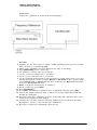
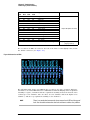
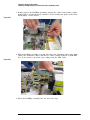
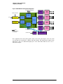
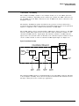
The Agilent Technologies Infiniium 90000 Oscilloscope at a Glance
Ease of use with high performance
The Agilent Technologies Infiniium oscilloscopes
combine unprecedented ease-of-use with highperformance digitizing oscilloscope functionality
to simplify your design and analysis measurement
tasks.
• Traditional oscilloscope front-panel interface
provides direct access to the controls needed
for most troubleshooting tasks.
• Graphical user interface with menus,
windows, dialogs boxes, and toolbars
provides easy access to dozens of
configuration and analysis tools, ensuring you
can set up and make the most complex
measurements.
• All models offer 80 GSa/s sampling rate on all
four channels.
• Models with bandwidths from 20 GHz to
63 GHz.
Display shows waveforms and graphical user
interface
• Graphical interface allows direct interaction
with waveforms, including drag-and-drop
positioning and instant waveform zoom.
• Touchscreen display allows oscilloscope
operation without an external pointing device.
• Waveforms displayed in color, making
correlation easy.
• Current configuration parameters displayed
near the waveform display and are colorcoded to make identification easy.
• Graphical interface menus and toolbars
simplify complex measurement setups.
Horizontal controls set sweep speed and position
• Intensified waveforms on main sweep
window make it easy to see what will appear
in the zoom window.
2
Acquisition and general controls start and stop
the oscilloscope and do basic setup
• Run and stop controls for continuous or single
acquisitions.
• Clear display before one or more acquisitions.
• Default setup and Autoscale set initial
configuration.
Hard disk drive and USB 2.0 port for saving and
restoring setups and measurement results
• Store measurement displays for inclusion in
reports and test setup guides.
• Store oscilloscope setups to repeat tests
another time.
• Hard disk stores oscilloscope operating
system.
Trigger setup controls set mode and basic
parameters
• Select Edge, Glitch, or Advanced Modes.
• Choose input source and slope.
• Use graphical user interface to simplify
configuration of pattern, state, delay, and
violation trigger modes.
• Use auxiliary trigger to increase triggering
flexibility.
Vertical controls set attenuation and position
• Color-coded knobs make it easy to find the
controls that affect each waveform.
Marker and quick measurements help measure
waveform parameters
• Waveform markers A and B to check voltage
or Δ-time at any point on the displayed
waveform.
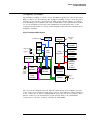
Service Policy
The service policy of this instrument requires
replacing defective assemblies. Some
assemblies can be replaced on an exchange
basis.
In This Service Guide
This guide provides the service information for the Agilent Technologies 90000 Q- Series
oscilloscopes. It is divided into seven chapters.
Chapter 1, "General Information," describes which oscilloscope models are covered by
this guide, supplied accessories, and where to find the specifications for the 90000 QSeries oscilloscopes.
Chapter 2, "Calibration," describes the types of calibrations, and how and when to run
the user calibration procedure.
Chapter 3, "Testing Performance," provides instructions for testing the oscilloscope to
verify that it performs according to specifications.
Chapter 4, "Troubleshooting," provides flowcharts and procedures for diagnosing
problems for assembly- level repair.
Chapter 5, "Replacing Assemblies," provides instructions for removing and replacing
assemblies in the oscilloscope.
Chapter 6, "Replaceable Parts," provides exploded parts diagrams and a list for ordering
replaceable parts.
Chapter 7, "Theory of Operation," describes the basic structure of the oscilloscope and
how its parts interact.
At the back of the book you will find safety notices.
3
4
1
Instruments covered by this service guide
Accessories supplied 7
Specifications and Characteristics 7
General Information
6
Instruments covered by this service guide
Oscilloscopes manufactured after the date this manual was released may be different
from those described in this manual. The release date of this manual is shown on the
title page. This manual will be revised when necessary.
If you have an oscilloscope that was manufactured after the release of this manual,
please check the Agilent Technologies website at www.agilent.com to see whether a
newer version of this manual is available.
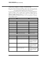
The following 90000 Q- Series oscilloscopes are covered in this guide.
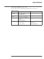
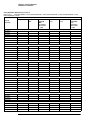
Oscilloscopes Covered by this Service Guide
Model
Bandwidth
DSOX/DSAX92004Q
20 GHz bandwidth
DSOX/DSAX92504Q
25 GHz bandwidth
DSOX/DSAX93304Q
33 GHz bandwidth
DSOX/DSAX95004Q
50 GHz bandwidth on 2 channels; 33 GHz bandwidth on 4 channels
DSOX/DSAX96204Q
62 GHz bandwidth on 2 channels; 33 GHz bandwidth on 4 channels
The oscilloscope model can be identified by the product number on the front or
rear panel.
6
Chapter 1: General Information
Accessories supplied
Accessories supplied
The following accessories are supplied.
• Mouse
• Stylus
• Keyboard
• Front panel cover
• Calibration cable (the 50 GHz and 62 GHz bandwidth models include a second
calibration cable for the RealEdge inputs)
• Connector Savers (qty. 5 for 20 GHz, 25 GHz, and 33 GHz; additional 2 for 50 GHz
and 62 GHz)
• Power cord (see parts list in chapter 6 for country- dependent part number)
Specifications and Characteristics
The following table contains a partial list of specifications and characteristics for the
Agilent Infiniium 90000 Q- Series oscilloscopes. For a full list of specifications and
characteristics, see the data sheets at www.agilent.com/find/90000q- series.
Specifications that are pertinent to each test are in the "Testing Performance" chapter.
Specifications are valid after a 30- minute warm- up period, and within ± 5° C from the
temperature at which the last self- calibration was performed.
Environment
Indoor use only.
Ambient
temperature
Operating 5 °C to +40 °C
Non-operating –40 °C to +65 °C
Humidity
Operating: up to 95% relative humidity (non-condensing) at +40 °C
Non-operating: up to 90% relative humidity at +65 °C
Altitude
Operating: up to 4,000 m (12,000 feet)
Non-operating: up to 15,300 meters (50,000 feet)
Installation/
Measurement
Category
Installation category: 2.
Measurement category: 1
Power Requirements
100-240 V, 47-63 Hz; 800 W Max for 4-channel models.
100-240 V, 50 Hz;100-208 V, 50/60 Hz; 800 W Max for 8-channel models.
Voltage Fluctuations
Note that the mains supply voltage fluctuations are not to exceed +/-10% of the
nominal supply voltage.
Pollution Degree
The Infiniium 90000 X-Series oscilloscopes may be operated in environments of
Pollution Degree 2.
Pollution Degree
Definitions
Pollution Degree 1: No pollution or only dry, non-conductive pollution occurs. The
pollution has no influence. Example: A clean room or climate-controlled office
environment.
Pollution Degree 2. Normally only dry non-conductive pollution occurs. Occasionally a
temporary conductivity caused by condensation may occur. Example: General indoor
environment.
Pollution Degree 3: Conductive pollution occurs, or dry, non-conductive pollution
occurs which becomes conductive due to condensation which is expected. Example:
Sheltered outdoor environment.
7
Chapter 1: General Information
Specifications and Characteristics
8
2
Running a self calibration
Calibration
11
Calibration
A calibration is simply an oscilloscope self- adjustment. The purpose of a calibration is
performance optimization.
There are three ways to calibrate an Infiniium oscilloscope:
• User mode, also known as a normal calibration, user calibration, or self calibration.
User mode includes the minimum set of calibrations and is intended to be run by
oscilloscope users. The user must be logged in as an administrator to run a self
calibration. In user mode you may choose to run time scale calibrations and interleave
correction calibrations, though those selections default to not run and they require
additional equipment. A self calibration for channels 1- 4 takes at least 4 hours to
complete, and an additional 4 hours for RealEdge channels 1R and 3R on 50 GHz
and 62 GHz models.
• Service mode, also known as a service calibration. A service calibration is performed
only by Agilent Service Center technicians. In service mode the 50 Ohm input
resistance calibration is performed, in addition to everything calibrated in the normal
mode. The time scale and interleave correction calibrations are run by default, though
they can be turned off. Additional equipment is required to run a service calibration.
A service calibration takes at least 4- 1/2 hours for channels 1- 4, and an additional
4- 1/2 hours for RealEdge channels 1R and 3R on 50 GHz and 62 GHz models.
• Factory mode, also known as a factory calibration. A factory calibration includes the
full set of calibrations, including time scale and interleave correction, and other
calibrations. A factory calibration is normally performed once during production of
the oscilloscope. All of the calibration factors are stored into flash RAM on the
acquisition board so that the calibration factors determined by the factory calibration
are preserved even if the hard drive is replaced or reformatted. Additional equipment
is required to perform a factory calibration on RealEdge channels.
The following section describes how to run a self calibration.
10
Chapter 2: Calibration
Running a self calibration
Running a self calibration
Let the Oscilloscope Warm Up Before Adjusting.
Warm up the oscilloscope for 30 minutes before starting the calibration procedure. Failure to allow warm
up may result in inaccurate calibration.
The self calibration uses signals generated in the oscilloscope to calibrate channel
sensitivity, offsets, and trigger parameters. There are three times we recommend
performing a self calibration:
• At least once a year
• When you replace the hard drive
• When the oscilloscope’s operating temperature (after the 30- minute warm- up period)
is more than ±5 °C different from that of the last calibration. Be sure to perform a
self calibration - - even if one was recently performed - - when environmental
temperature conditions cause the oscilloscope’s operating temperature to change, such
as when the oscilloscope is moved to a test rack or chamber.
Equipment Required
Equipment
Critical Specifications
Agilent Part Number
Connector Savers (5 supplied
with oscilloscope)
3.5 mm (f) to 3.5 mm (f)
Agilent 54916-68717 (for all oscilloscope
models, channels 1-4)
Connector Savers (2 supplied
with 50 GHz and 62 GHz
models)
1.85 mm (f) to 1.85 mm (f)
Agilent 54932-68712 (for 50 GHz and
62 GHz models, channels 1R and 3R)
Cable assembly
50 Ohm characteristic impedance BNC
(m) connectors, 36 inches (91 cm) to 48
inches (122 cm) long
Agilent 8120-1840
Adapter
SMA(m) to BNC(f)
Agilent 1250-1200
Cable (supplied with
oscilloscope)
No substitute
Agilent 54916-61626 (for all oscilloscope
models, channels 1-4)
Agilent 54932-61630 (for 50 GHz and
62 GHz models, channels 1R and 3R)
Calibration time
It will take approximately 4-1/2 hours to run the self calibration on channels 1-4 on the oscilloscope, plus
4-1/2 more hours to calibrate RealEdge channels 1R and 3R, including the time required to change cables
from channel to channel.
1 Let the oscilloscope warm up before running the self calibration.
The self calibration should be done only after the oscilloscope has run for 30 minutes
at ambient temperature with the cover installed. Calibration of an oscilloscope that has
not warmed up may result in an inaccurate calibration.
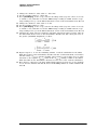
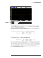
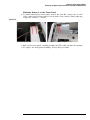
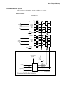
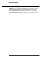
2 Select Utilities > Calibration.
3 Uncheck the Cal Memory Protect box.
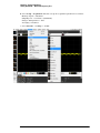
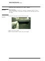
You cannot run a self calibration if this box is checked. See Figure 2- 1 for an example
screen showing RealEdge channels.
11
Chapter 2: Calibration
Running a self calibration
Figure 2-1 Calibration Dialog Box
Clear this check
box before starting
calibration
Click here to start
calibration
4 Click Start, then follow the instructions on the screen.
The routine will ask you to do the following steps:
a Disconnect everything from all inputs and Cal Out.
b Indicate whether you want to run time scale and interleave correction calibrations.
For a list of equipment required to perform the time scale calibration, refer to
the “Time Scale Accuracy (TSA) Test” section in the next chapter. The interleave
correction calibration requires a sine wave generator and a ≥ 67 GHz cable with
1.85 mm male connectors on each end. You will also need to use the two supplied
1.85 mm (f)- (f) connector savers. To learn more about both calibration options,
click Help.
c Connect the calibration cable from Cal Out to channel 1.
You must use the 54916- 61626 cable (channels 1- 4) or 54932- 61630 cable
(channels 1R and 3R) with two connector saver adapters for all oscilloscopes.
Failure to use the appropriate calibration cable will result in an inaccurate
calibration.
d Connect the calibration cable from Cal Out to each of the channel inputs as
requested.
e When instructed, connect the calibration cable from the Cal Out on the front
panel of the oscilloscope to the 1250- 1200 SMA(m) to BNC(f) adapter and then
connect the other end of the 1250- 1200 adapter to the 8120- 1840 BNC cable.
Connect the other end of the BNC cable to the Trig In on the rear of the
oscilloscope.
f A Passed/Failed indication appears for each calibration section. If any section
fails, click the Details box for information on the failures. Also check the
calibration cables.
5 After the calibration procedure is completed, click Close.
12
3
Vertical Performance Verification 15
Offset Accuracy Test 16
DC Gain Accuracy Test 23
Analog Bandwidth - - Maximum Frequency Test
Time Scale Accuracy (TSA) Test 37
Performance Test Record 39
Testing Performance
28
This section describes performance test procedures.
Performance Test Interval
The procedures in this section may be performed for incoming inspection and should
be performed periodically to verify that the oscilloscope is operating within specification.
The recommended test interval is once per year or after 2000 hours of operation.
Performance should also be tested after repairs or major upgrades.
Performance Test Record
A test record form is provided at the end of this section. This record lists performance
tests and test limits, and provides space to record test results.
Test Order
The tests in this section may be performed in any order. However, it is recommended
to conduct the tests in the order presented in this manual as this represents an
incremental approach to performance verification. This may be useful if you are
attempting to troubleshoot a suspected problem.
Test Equipment
Lists of equipment needed to conduct each test are provided for each test procedure.
The procedures are written to minimize the number and types of oscilloscopes and
accessories required. The oscilloscopes in these lists are ones that are currently available
for sale by Agilent at the time of writing this document. In some cases, the test
procedures use features specific to the oscilloscopes in the recommended equipment
list. However, the oscilloscopes, cables, and accessories that satisfy the critical
specifications in these lists may be substituted for the recommended models with some
modification to the test procedures.
Contact Agilent Technologies for more information about the Agilent products in these
lists.
14
Chapter 3: Testing Performance
Vertical Performance Verification
This section contains the following vertical performance verification tests:
•
•
•
•
Offset Accuracy Test
DC Gain Accuracy Test
Analog Bandwidth - - Maximum Frequency Test
Time Scale Accuracy (TSA) Test
15
Offset Accuracy Test
CAUTION
Ensure that the input voltage to the oscilloscope never exceeds ±5 V.
Let the oscilloscope warm up before testing.
The oscilloscope under test must be warmed up (with the oscilloscope application running) for at least
30 minutes prior to the start of any performance test.
Specifications
Offset Accuracy
≤ 3.5 V: ±(2% of channel offset + 1% of full scale + 1 mV)
> 3.5 V: ±(2% of channel offset + 1% of full scale)
Full scale is defined as 8 vertical divisions. Magnification is used below 10 mV/div. Below 10
mV/div, full scale is defined as 80 mV. The major scale settings are 10 mV, 20 mV, 50 mV, 100
mV, 200 mV, 500 mV and 1 V.
Equipment Required
Description
Critical Specifications
Recommended
Model/
Part Numbers
Digital Multimeter
DC voltage measurement accuracy better than ±0.1% of reading
Agilent 34411A
Cable Assembly
(2 required)
50 ohm characteristic impedance, BNC (m) connectors
Agilent 8120-1840
Adapter
BNC Tee (m)(f)(f)
Agilent 1250-0781
Adapter
BNC (f) to dual banana
Agilent 1251-2277
Connector Saver
3.5 mm (f)-(f), shipped with each 90000 Q-Series oscilloscope
Agilent 5061-5311 (used
with 20, 25, and 32 GHz
oscilloscope models)
2.4 mm (f) to 3.5 mm (f) adapter
Agilent 11901B (used
with 50 GHz and 62 GHz
oscilloscope models)
BNC (f) to SMA (m) Adapter
Agilent 1250-1200
Adapter
(2 required)
NOTE: The offset accuracy specification has two terms ±(offset gain + zero error). The
offset gain specification is ±2% of channel offset while the zero error specification is
±(1% of full scale + 1mV) for ≤ 3.5 V and 1% of full scale > 3.5 V. The offset accuracy test procedure
tests each of these terms individually.
Zero Error Test Procedure
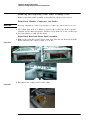
1 Disconnect all cables from the scope channel inputs.
2 Press [Default Setup], then configure the scope as follows:
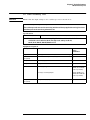
a Select Setup > Acquisition.
16
Chapter 3: Testing Performance
Offset Accuracy Test
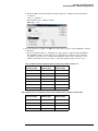
b When the Acquisition Setup window appears, enable averaging and set the # of
averages to 256 as shown below.
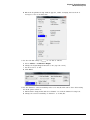
3 Configure the scope to measure Average voltage on channel 1 as follows:
a Change the vertical scale of channel 1 to 10 mV/div.
b Click the V avg measurement on the left side of the screen.
V avg
measurement
17
Chapter 3: Testing Performance
Offset Accuracy Test
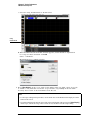
c When the Enter Measurement Info window appears, ensure that the V avg function
is set up as follows and then click OK:
Source = Channel 1
Measurement Area = Entire Display
4 Press [Clear Display] on the scope and wait for the #Avgs value (top right corner of
screen) to return to 256. Record the scope's mean V avg reading in the Zero Error Test
section of the Performance Test Record.
Notes
• For all scope readings in this procedure, use the mean value in the Measurements display area at the
bottom of the screen.
• If a question mark appears in front of any of the values at the bottom of the screen, press [Clear Display]
on the scope, wait for the #Avgs value to return to 256, and then record the scope reading.
Record the
mean reading
5 Change the vertical scale of channel 1 to 20 mV/div, press [Clear Display], wait for the
#Avgs value (top right corner of screen) to return to 256, and then record the scope
V avg reading in the Zero Error Test section of the Performance Test Record.
18
Chapter 3: Testing Performance
Offset Accuracy Test
6 Repeat step 5 for the remaining vertical sensitivities for channel 1 in the Zero Error
Test section of the Performance Test Record.
7 Press [Default Setup], then turn off channel 1 and turn the channel 2 display on.
8 Configure the scope to measure V avg on Channel 2 as follows:
a Select Setup > Acquisition. When the Acquisition Setup window appears, enable
averaging and set the # of averages to 256.
b Change the vertical sensitivity of channel 2 to 10 mV/div.
c Click the V avg measurement icon on the left side of the screen.
d When the Enter Measurement Info window appears, ensure that the Vavg function
is set up as follows and then click OK:
Source = Channel 2
Measurement area = Entire Display
9 Press [Clear Display] on the scope, wait for the #Avgs value to return to 256, and then
record the scope’s mean V avg reading in the Zero Error Test section of the Performance
Test Record.
10 Repeat step 9 for the remaining vertical sensitivities for channel 2 in the Zero Error
section of the Performance Test Record.
11 Repeat steps 7 through 10 for channels 3 and 4, and for channels 1R (RealEdge) and
3R for 50 GHz and 62 GHz models. Press the RealEdge button to enable channels 1R
and 3R.
19
Chapter 3: Testing Performance
Offset Accuracy Test
Offset Gain Test Procedure
1 Make the connections to scope channel 1 as shown below.
Connections
Oscilloscope Channel Input
Cal Out on Oscilloscope Front Panel
Connection Saver
Connection Saver
BNC (f) to SMA (m) adapter
BNC (f) to SMA (m) adapter
Notes:
• Where the BNC Tee adapter is used, it is important to connect it directly to the scope channel input
using the BNC (f) to SMA (m) adapter and the connection savers to minimize ground potential
differences and to ensure that the DMM measures the input voltage to the scope channel as accurately
as possible. Differences in ground potential can be a significant source of measurement error,
particularly at high scope sensitivities.
• It also helps to reduce ground potential differences if the scope and DMM are connected to the same
AC supply circuit.
• 256 averages are used in the scope measurements of this section to reduce measurement noise and to
reduce the measurement error due to resolution.
2 Set up the DMM to perform DC voltage measurements.
3 Configure the scope to measure V avg on Channel 1 as follows:
a Press [Default Setup].
b Select Setup > Acquisition. When the Acquisition Setup window appears, enable
averaging and set the # of averages to 256.
c Click the V avg measurement icon on the left side of the screen.
d When the Enter Measurement Info window appears, ensure that the V avg function
20
Chapter 3: Testing Performance
Offset Accuracy Test
is set up as follows and then click OK:
Source = Channel 1
Measurement area = Entire Display
4 Set the channel 1 offset value to 400.0 mV. This can be done using the front
panel control or:
a Pull down the Setup menu and select Channel 1 or click the Channel 1 setup icon.
b Change the vertical sensitivity (Scale) of channel 1 to 10 mV/div.
c Click the Offset control arrows to change the offset value or click on the offset
value and enter 400.0 mV in the dialog box.
Channel 1
setup icon
5
Set the Cal Out voltage (VCal Out) to +400.0 mV as follows:
a Select Utilities > Calibration Output.
b Change the Signal Output function to DC (top left corner).
c Set the Level to 400.0 mV.
d Click Close.
6 Press [Clear Display] on the scope, wait for the #Avgs value (top right corner of screen)
to return to 256, and then record the DMM voltage reading as VDMM+ and the scope
Vavg reading as VScope+ in the Offset Gain Test section of the Performance Test Record.
21
Chapter 3: Testing Performance
Offset Accuracy Test
7 Change the channel 1 offset value to - 400.0 mV.
8 Set the Cal Out voltage to - 400.0 mV.
9 Press [Clear Display] on the scope, wait for the #Avgs value (top left corner of screen)
to return to 256, and then record the DMM voltage reading as VDMM- and the scope
Vavg reading as VScope- in the Offset Gain Test section of the Performance Test Record.
10 Change the channel 1 offset value to 0 mV.
11 Set the Cal Out voltage to 0 mV.
12 Press [Clear Display] on the scope, wait for the #Avgs value (top left corner of screen)
to return to 256, and then record the DMM voltage reading as VDMM0 and the scope
Vavg reading as VScope0 in the Offset Gain Test section of the Performance Test Record.
13 Calculate the offset gain error using the following expressions and record the value in
the Offset Gain Test section of the Performance Test Record. The offset gain error is
the greater (maximum magnitude) of either:
scope+ – V scope0
V
------------------------------------------ – 1 100
V DMM+ – V DMM0
or
scope- – V scope0
V
----------------------------------------- – 1 100
V DMM- – V DMM0
14 Repeat steps 4 to 13 for the remaining channel 1 vertical sensitivities in the Offset
Gain Test section of the Performance Test Record. For each measurement, set both the
Cal Out voltage (VCal Out) and the Channel offset voltage to the positive VCal Out value
and then to the negative VCal Out value in the "VCal Out Setting" column of the Offset
Gain Test table in the Performance Test Record for each of the vertical sensitivities.
15 Move the Tee connector to the next channel input and repeat steps 4 to 13 for channels
2 to 4 and for channels 1R and 3R. Press the RealEdge button to enable channels 1R
and 3R.
22
Chapter 3: Testing Performance
DC Gain Accuracy Test
DC Gain Accuracy Test
CAUTION
Ensure that the input voltage to the oscilloscope never exceeds ±5 V.
Let the oscilloscope warm up before testing.
The oscilloscope under test must be warmed up (with the oscilloscope application running) for at least
30 minutes prior to the start of any performance test.
Specifications
DC Gain Accuracy
±2% of full scale at full resolution channel scale (±2.5% for 5 mV/div)
Full scale is defined as 8 vertical divisions. Magnification is used below 10 mV/div. Below 10
mV/div full scale is defined as 80 mV. The major scale settings are 10 mV,
20 mV, 50 mV, 100 mV, 200 mV, 500 mV and 1 V.
Equipment Required
Description
Critical Specifications
Recommended
Model/
Part Numbers
Digital Multimeter
DC voltage measurement accuracy better than ±0.1% of reading
Agilent 34411A
Cable Assembly
(2 required)
50Ω characteristic impedance, BNC (m) connectors
Agilent 8120-1840
Adapter
BNC Tee (m)(f)(f)
Agilent 1250-0781
Adapter
BNC (f) to dual banana
Agilent 1251-2277
Connector Saver
3.5 mm (f)-(f), shipped with each 90000 Q-Series oscilloscope
Agilent 5061-5311 (used
with 20, 25, and 32 GHz
oscilloscope models)
2.4 mm (f) to 3.5 mm (f) adapter
Agilent 11901B (used
with 50 GHz and 62 GHz
oscilloscope models)
BNC (f) to SMA (m) Adapter
Agilent 1250-1200
Adapter
(2 required)
23
Chapter 3: Testing Performance
DC Gain Accuracy Test
Procedure
1 Make the connections to scope channel 1 as shown below.
Connections
Oscilloscope Channel Input
Cal Out on Oscilloscope Front Panel
Connection Saver
Connection Saver
BNC (f) to SMA (m) adapter
BNC (f) to SMA (m) adapter
Notes:
• Where the BNC Tee adapter is used, it is important to connect it directly to the scope channel input
using the BNC (f) to SMA (m) adapter and the connection saver to minimize ground potential
differences and to ensure that the DMM measures the input voltage to the scope channel as accurately
as possible. Differences in ground potential can be a significant source of measurement error,
particularly at high scope sensitivities.
• It also helps to reduce ground potential differences if the scope and DMM are connected to the same
AC supply circuit.
• 256 averages are used in the scope measurements of this section to reduce measurement noise and to
reduce the measurement error due to resolution.
2 Press [Default Setup], then configure the scope as follows:
a Select Setup > Acquisition.
24
Chapter 3: Testing Performance
DC Gain Accuracy Test
b When the Acquisition Setup window appears, enable averaging and set the # of
averages to 256 as shown below.
3 Set the Cal Out voltage (VCal Out) to +30 mV as follows:
a Select Utilities > Calibration Output.
b Change the Signal Output function to DC (top left corner).
c Set the Level to 30 mV.
d Click Close.
4 Set the channel 1 vertical sensitivity value to 10 mV/div. This can be done either using
the front panel control or:
a Pull down the Setup menu and select Channel 1 or click the Channel 1 setup icon.
b Change the vertical sensitivity of channel 1 to 10 mV/div.
25
Chapter 3: Testing Performance
DC Gain Accuracy Test
c Select the Vavg measurement as shown below.
V avg
measurement
d When the Enter Measurement Info window appears, ensure that the V avg function
is set up as follows and then click OK:
Source = Channel 1
Measurement Area = Entire Display
5 Press [Clear Display] on the scope, wait for the #Avgs value (top right corner of screen)
to return to 256, and then record the scope's mean V avg reading in the DC Gain
Accuracy Test section of the Performance Test Record.
Notes
• For all scope readings in this procedure, use the mean value in the Measurements display area at the
bottom of the screen.
• If a question mark appears in front of any of the values at the bottom of the screen, press [Clear Display]
on the scope, wait for the #Avgs value to return to 256, and then record the scope reading.
26
Chapter 3: Testing Performance
DC Gain Accuracy Test
Record the
mean reading
6 Change the Cal Out voltage to - 30 mV.
7 Press [Clear Display] on the scope, wait for the #Avgs value to return to 256 and then
record the DMM voltage reading and the scope V avg reading in the DC Gain Test
section of the Performance Test Record.
8 Calculate the DC gain using the following expression and record this value in the DC
Gain Test section of the Performance Test Record.
For vertical sensitivities of less than 1 volt use the following equation:
ΔV out
V scope+ – V scopeDCGainError = -------------- = ----------------------------------------- – 1 ⋅ 75
ΔV in
V DMM+ – V DMM-
For vertical sensitivity = 1 V use the following equation:
ΔV out
V scope+ – V scopeDCGainError = -------------- = ----------------------------------------- – 1 ⋅ 60
ΔV in
V DMM+ – V DMM9 Repeat steps 3 to 8 for the remaining channel 1 vertical sensitivities in the DC Gain
Test section of the Performance Test Record. For each measurement, set both the Cal
Out voltage (VCalOut) and the Channel offset voltage to the positive VCalOut value and
then to the negative VCalOut value in the “VCalOut Setting” column of the DC Gain Test
table in the Performance Test Record for each of the vertical sensitivities.
10 Move the Tee connector to the next channel input and repeat steps 3 to 9 for channels
2 to 4 and for channels 1R and 3R.
27
Chapter 3: Testing Performance
Analog Bandwidth -- Maximum Frequency Test
Analog Bandwidth - - Maximum Frequency Test
CAUTION
Ensure that the input voltage to the oscilloscope never exceeds ±5 V.
Let the oscilloscope warm up before testing.
The oscilloscope under test must be warmed up (with the oscilloscope application running) for at least
30 minutes prior to the start of any performance test.
Specification
Analog Bandwidth (-3 dB)
DSO/DSAX92004Q
20.0 GHz
DSO/DSAX92504Q
25.0 GHz
DSO/DSAX93304Q
32.0 GHz
DSO/DSAX95004Q
50.0 GHz
DSO/DSAX96204Q
62.0 GHz
Equipment Required
Description
Critical Specifications
Recommended Model/
Part Numbers
Microwave CW
Generator
Maximum Frequency ≥ 32 GHz
Power range: -20 dBm to +16 dBm into 50 ohm
Output resistance = 50 ohm
Agilent E8257D with Opt 540 (used
with 20, 25, and 32 GHz
oscilloscope models) or Opt 567
(used with all models)
Maximum Frequency ≥ 67 GHz
Power range: -20 dBm to +25 dBm into 50 ohm
Output resistance = 50 ohm
Agilent E8257D with Opt 567 (used
with 50 GHz and 62 GHz
oscilloscope models)
2 Resistor Power Splitter
Max Frequency ≥ 32 GHz
Agilent 11667C (used with 20, 25,
and 32 GHz oscilloscope models)
2 Resistor Power Splitter
Max Frequency ≥ 65 GHz
Anritsu V241C (used with 50 GHz
and 62 GHz oscilloscope models)
Power Meter
Agilent P-series with power sensor compatibility
Agilent N1912A
Power Sensor
Maximum Frequency ≥ 32 GHz
Power range: -24 dBm to +23 dBm
Agilent N1922A (used with 20, 25,
and 32 GHz oscilloscope models)
Maximum Frequency ≥ 67 GHz
Power range: -35 dBm to +20 dBm
Agilent N8488A (used with 50 GHz
and 62 GHz oscilloscope models)
50 ohm Characteristic Impedance
2.4 mm (m) to 2.4 mm (m) connectors
Max Frequency ≥ 32 GHz
Agilent N5180-60204 (used with
20, 25, and 32 GHz oscilloscope
models)
1.85 mm (m) to 1.85 mm (m) 50 ohm
Max Frequency ≥ 67 GHz
Gore 0F0CB0CB036.0 (67 GHz)
(used with 50 GHz and 62 GHz
oscilloscope models)
Adapter
2.4 mm (m) to 3.5 mm (m) (qty. 1)
Agilent 11901A (used with 20, 25,
and 32 GHz oscilloscope models)
Adapter
2.4 mm (m) to 3.5 mm (f) (qty. 2)
Agilent 11901C (used with 20, 25,
and 32 GHz oscilloscope models)
Power Splitter
Microwave Cable
28
Chapter 3: Testing Performance
Analog Bandwidth -- Maximum Frequency Test
Description
Critical Specifications
Recommended Model/
Part Numbers
Connector Saver
3.5 mm (f)-(f), shipped with 20, 25, and 32 GHz
oscilloscope models
Agilent 5061-5311 (used with 20,
25, and 32 GHz oscilloscope
models)
29
Chapter 3: Testing Performance
Analog Bandwidth -- Maximum Frequency Test
Connections for all oscilloscope models, channels 1- 4
Microwave CW
Generator E8257D
Power meter
N1912A
Oscilloscope
Power splitter
11667C
Connection saver
Power sensor
cable
11901A adapter
Microwave cable
Power sensor
N1922A
11901C adapter
Notes
• Connect output 1 of the 11667C splitter to the scope Channel n input directly using the 11901A adapter
and a connector saver, without any additional cabling or adapters.
• Connect the power sensor directly to output 2 of the power splitter using the 11901C adapter without
any additional cabling or adapters.
• Connect the microwave cable directly to output 3 of the power splitter using the 11901C adapter
without any additional cabling or adapters.
• Minimize the use of other adapters.
• Ensure that 2.4 mm and 3.5 mm connectors are tightened properly:
8 in-lbs (90 N-cm) for 3.5 mm
8 in-lbs (90 N-cm) for 2.4 mm
30
Chapter 3: Testing Performance
Analog Bandwidth -- Maximum Frequency Test
Connections for 50 and 62 GHz oscilloscope models, channels 1R- 3R
Microwave CW
Generator E8257D
Power meter
N1912A
Oscilloscope
Power splitter
Anritsu V241C
Power sensor
cable
Power sensor
N8488A
Microwave cable
Gore 67 GHz
Notes
• Connect output 1 of the V241C splitter to the scope Channel n input directly without any additional
cabling or adapters.
• Minimize the use of any adapters.
• Ensure that 1.85 mm connectors are tightened properly:
8 in-lbs (90 N-cm) for 1.85 mm
Procedure
1 Preset the power meter.
2 Ensure that the power sensor is disconnected from any source and zero the meter.
3 Connect the power sensor to the power meter's Power Ref connector and calibrate the
meter.
4 Make the connections to oscilloscope channel 1 as shown in the connection diagram
above.
5 Set up the Power Meter to display measurements in units of Watts.
6 Press [Default Setup], then configure the scope as follows:
a Ensure Channel 1 is displayed and all other channels are turned off.
b Set the vertical scale of channel 1 to 10 mV/div.
c Set the horizontal scale to 16 ns/div (to display 8 cycles of a 50 MHz waveform).
Click here and enter 16 ns
31
Chapter 3: Testing Performance
Analog Bandwidth -- Maximum Frequency Test
d Select Setup > Acquisition and then set up the acquisition parameters as follows:
Memory Depth = Automatic
Sampling rate = 160 GSa/s (maximum)
Sin(x)/x Interpolation = Auto
Averaging = Disabled
e Select Measure > Voltage > V rms.
32
Chapter 3: Testing Performance
Analog Bandwidth -- Maximum Frequency Test
f When the Enter Measurement Info window appears, configure this measurement
as follows:
Source = Channel 1
Measurement Area = Entire Display
RMS Type = AC
7 Set the generator to apply a 50 MHz sine wave with a peak- to- peak amplitude of about
4 divisions.
• Use the following tables to determine the approximate required signal amplitude.
The amplitude values in the tables are not absolutely required. If your generator
is unable to produce the recommended amplitude, then set the generator to the
highest value that does not produce a vertically clipped signal on the scope.
Table 3-1. Nominal Generator Amplitude Settings for all Oscilloscope Models, channels 1-4
Scope
Vertical Sensitivity
Generator Signal
Amplitude (Vp-p)
Generator Signal
Amplitude (dBm)
10 mV/div
0.08
-18
20 mV/div
0.16
-12
50 mV/div
0.4
-4
100 mV/div
0.8
+2
200 mV/div
1.6
+8
500 mV/div
4.0
+16
1 V/div
6.3
+20
Table 3-2. Nominal Generator Amplitude Settings for 50 and 62 GHz Oscilloscope Models, channels 1R-3R
Scope
Vertical Sensitivity
Generator Signal
Amplitude (Vp-p)
Generator Signal
Amplitude (dBm)
10 mV/div
0.08
-12.5
20 mV/div
0.16
-9.5
50 mV/div
0.4
-5.5
100 mV/div
0.8
-2.5
33
Chapter 3: Testing Performance
Analog Bandwidth -- Maximum Frequency Test
8 Measure the input power to the scope channel and convert this measurement to Volts
RMS using the expression:
V in =
P meas × 50Ω
For example, if the power meter reading is 4.0 μW, then Vin = (4.0*10- 6 * 50Ω)1/2 =
14.1 mVrms.
Record the RMS voltage in the Analog Bandwidth - Maximum Frequency Check section
of the Performance Test Record (Vin @ 50 MHz).
9 Press [Clear Display] on the scope and record the scope V rms reading in the Analog
Bandwidth - Maximum Frequency Check section of the Performance Test Record (Vout
@ 50 MHz).
Notes
• For all scope readings in this procedure, use the mean value in the Measurements display area at the
bottom of the screen.
Record the
mean reading
10 Calculate the reference gain as follows:
V out @50 MHz
Gain 50 MHz = ------------------------------V in @50 MHz
Record this value in the Calculated Gain @50 MHz column in the Analog Bandwidth Maximum Frequency Check section of the Performance Test Record.
34
Chapter 3: Testing Performance
Analog Bandwidth -- Maximum Frequency Test
11 Change the generator frequency to the maximum value for the model being tested as
shown in the table below. It is not necessary to adjust the signal amplitude at this
point in the procedure.
Setting
Model
DSOX/DSAX 92004Q
(channels 1-4)
DSOX/DSAX 92504Q
(channels 1-4)
DSOX/DSAX 93304Q,
95004Q, and 96204Q
(channels 1-4)
Maximum Frequency
20 GHz
25 GHz
32 GHz
Scope Time Base Setting
50 ps/div
50 ps/div
50 ps/div
Model
DSOX/DSAX95004Q
(channels 1R, 3R)
DSOX/DSAX 96204Q
(channels 1R, 3R)
Maximum Frequency
50 GHz
62 GHz
Scope Time Base Setting
16 ps/div
16 ps/div
12 Change the scope time base to the value for the model under test in the table above.
Click here and enter time
base value from table
13 Measure the input power to the scope channel at the maximum frequency and convert
this measurement to Volts RMS using the expression:
V in =
P meas × 50Ω
For example, if the power meter reading is 4.0 μW, then Vin = (4.0*10- 6 * 50Ω)1/2 =
14.1 mVrms.
Record the RMS voltage in the Analog Bandwidth - Maximum Frequency Check section
of the Performance Test Record (Vin @ Max Freq).
14 Press [Clear Display] on the scope and record the scope V rms reading in the Analog
Bandwidth - Maximum Frequency Check section of the Performance Test Record (Vout
@ Max Freq).
15 Calculate the gain at the maximum frequency using the expression:
Gain Max Freq = 20 log 10
( V out Max Freq ) ⁄ ( V in Max Freq )
-----------------------------------------------------------------------------Gain 50 MHz
For example, if (Vout @ Max Frequency) = 13.825 mV, (Vin @ Max Frequency) = 13.461
mV and Gain @ 50MHz = 1.0023, then:
13.825 mV ⁄ 13.461 mV
Gain Max Freq = 20 log 10 ------------------------------------------------------------- = 0.212 dB
1.0023
Record this value in the Calculated Gain @Max Freq column in the Analog Bandwidth
- Maximum Frequency Check section of the Performance Test Record. To pass this test,
this value must be greater than - 3.0 dB.
35
Chapter 3: Testing Performance
Analog Bandwidth -- Maximum Frequency Test
16 Change the scope setup as follows:
a Change the channel vertical sensitivity to 20 mV/div.
b Reset the horizontal scale to 16 ns/div (to display 8 cycles of a 50 MHz waveform).
17 Change the generator output as follows:
a Reset the generator frequency to 50 MHz.
b Change the amplitude to the value suggested for this sensitivity in Table 3- 1.
18 Repeat steps 8, 9, and 10 to measure the reference gain at 50 MHz for this sensitivity.
19 Repeat steps 11, 12, 13, and 14 to measure the gain at maximum frequency for this
sensitivity.
20 Repeat steps 15 to 19 to complete measuring gains for remaining sensitivities for channel
1 in the Analog Bandwidth - Maximum Frequency Check section of the Performance
Test Record.
21 Move the splitter to channel 2 and change the scope configuration as follows:
• Ensure Channel 2 is displayed and all other channels are turned off.
• Set the vertical sensitivity of channel 2 to 10 mV/div.
• Set the horizontal scale to 16 ns/div (to display 8 cycles of a 50 MHz waveform).
• Right click on the V rms measurement at the bottom of the screen. When the RMS
voltage measurement setup window appears, change the source from Channel 1 to
Channel 2.
22 Repeat steps 7 to 20 to complete measuring gains for channel 2.
23 Move the splitter to channel 3 and change the scope configuration as follows:
a Ensure Channel 3 is displayed and all other channels are turned off.
b Set the vertical sensitivity of channel 3 to 10 mV/div.
c Set the horizontal scale to 16 ns/div (to display 8 cycles of a 50 MHz waveform).
d Click on the V rms measurement at the bottom of the screen and select Customize.
When the V rms setup window appears, change the source from Channel 2 to
Channel 3.
24 Repeat steps 7 to 20 to complete measuring gains for channel 3.
25 Move the splitter to channel 4 and change the scope configuration as follows.
a Ensure Channel 4 is displayed and all other channels are turned off.
b Set the vertical sensitivity of channel 4 to 10 mV/div.
c Set the horizontal scale to 16 ns/div (to display 8 cycles of a 50 MHz waveform).
d Click on the V rms measurement at the bottom of the screen. When the V rms
setup window appears, change the source from Channel 3 to Channel 4.
26 Repeat steps 7 to 20 to complete measuring gains for channel 4.
27 Press the RealEdge button to enable channels 1R and 3R.
28 Repeat steps 7 to 22 for channels 1R and 3R, using Table 3- 2 in step 17.
36
Chapter 3: Testing Performance
Time Scale Accuracy (TSA) Test
Time Scale Accuracy (TSA) Test
This procedure verifies the maximum TSA specification for the oscilloscope.
Equipment Required
Equipment
Critical Specifications
Recommended Model/Part
Synthesized sine
wave source
Output Frequency: ≥ 10 MHz
Output Amplitude: 0 dBm
Frequency Resolution: 0.1 Hz
Agilent E8257D PSG
10 MHz frequency
reference
Output Frequency: 10 MHz
Absolute Freq. Error: < ±0.0275 ppm
Agilent 53132A opt. 012 frequency counter
RF cable
50 ohm characteristic impedance (no
substitute)
BNC (m) connectors
Max Frequency: ≥ 50 MHz
Agilent 8120-1840
Adapters, assorted
3.5 mm (f) to Precision BNC (m)
3.5 mm (f) to 3.5 mm (f)
Agilent 54855-67604
Agilent 83059B
2.4 mm (f) to 2.92 mm (f)
Rosenberger 02K109-K00S3
37
Chapter 3: Testing Performance
Time Scale Accuracy (TSA) Test
Connections
Connect the equipment as shown in the following figure.
1
2
3
4
5
6
7
8
9
10
11
12
13
14
15
Procedure
Configure the sine wave source to output a 0 dBm (600 mVpp) sine wave into 50 ohms
with a frequency of 10.00002000 MHz.
Adjust source amplitude such that displayed sine wave is 600 mVpp.
Press [Default Setup] on the oscilloscope.
Set channel 1's vertical scale to 100 mV/div.
Set the oscilloscope sample rate to 100 kSa/s.
Set the scope's horizontal scale to 20 ms/div.
Set the measurement thresholds for all waveforms to a fixed voltage level of 0 V and
±20 mV hysteresis. To do this, go under Measure > Thresholds in the top menu. Then
select Custom: level +/- Hysteresis and enter 20 mV into the Hysteresis field and 0
V into the Threshold Level field.
Enable a frequency measurement on channel 1.
On the oscilloscope, press [Stop].
Press [Clear Display].
Press [Run], wait until 10 acquisitions have accumulated, and then press [Stop].
Convert the average frequency value to time scale error by subtracting 20 Hz and
dividing by 10 Hz/ppm.
Record the time since calibration (in years) in the table. The calibration date can be
found in the Calibration menu window.
Calculate the test limits using the following formula and record them in the table.
Test Limits = ±(0.100 + 0.100 x Years Since Calibration)
Record the results in the Performance Test Record.
38
Chapter 3: Testing Performance
Performance Test Record
Performance Test Record
Agilent Technologies
Agilent 90000 Q-Series Oscilloscopes
Model Number _____________________
Tested by___________________
Serial Number ___________________________
Work Order No.___________________
Recommended Test Interval - 1 Year/2000 hours
Date___________________
Recommended next test date ___________________
Ambient temperature ___________________
Offset Accuracy Test
Zero Error Test
Vertical
Sensitivity
10 mV/div
20 mV/div
50 mV/div
100 mV/div
200 mV/div
500 mV/div
1 V/div
Test Limits
Channel 1
Channel 2
Channel 3
Channel 4
Channel 1R
Channel 3R
-1.8 mV to +1.8 mV
-2.6 mV to +2.6 mV
-5.0 mV to +5.0 mV
-9.0 mV to +9.0 mV
-17.0 mV to +17.0 mV
-41.0 mV to +41.0 mV
-81.0 mV to +81.0 mV
39
Chapter 3: Testing Performance
Performance Test Record
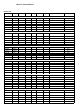
Offset Gain Test
Vertical
Sensitivity
Channel 1
10 mV/div
20 mV/div
50 mV/div
100 mV/div
200 mV/div
500 mV/div
1 V/div
Channel 2
10 mV/div
20 mV/div
50 mV/div
100 mV/div
200 mV/div
500 mV/div
1 V/div
Channel 3
10 mV/div
20 mV/div
50 mV/div
100 mV/div
200 mV/div
500 mV/div
1 V/div
Channel 4
10 mV/div
20 mV/div
50 mV/div
100 mV/div
200 mV/div
500 mV/div
1 V/div
Channel 1R
10 mV/div
20 mV/div
50 mV/div
100 mV/div
200 mV/div
500 mV/div
1 V/div
Channel 3R
10 mV/div
20 mV/div
50 mV/div
100 mV/div
200 mV/div
500 mV/div
1 V/div
VCal Out
Setting
VDMM
+
VDMM-
VDMM0
VScope+
VScope-
VScope0
Calc. Offset
Gain Error
Offset Gain Error
Test Limits
±400 mV
±400 mV
±700 mV
±1.2 V
±2.2 V
±2.4 V
±2.4 V
±2 %
±2 %
±2 %
±2 %
±2 %
±2 %
±2 %
±400 mV
±400 mV
±700 mV
±1.2 V
±2.2 V
±2.4 V
±2.4 V
±2 %
±2 %
±2 %
±2 %
±2 %
±2 %
±2 %
±400 mV
±400 mV
±700 mV
±1.2 V
±2.2 V
±2.4 V
±2.4 V
±2 %
±2 %
±2 %
±2 %
±2 %
±2 %
±2 %
±400 mV
±400 mV
±700 mV
±1.2 V
±2.2 V
±2.4 V
±2.4 V
±2 %
±2 %
±2 %
±2 %
±2 %
±2 %
±2 %
±400 mV
±400 mV
±700 mV
±1.2 V
±2.2 V
±2.4 V
±2.4 V
±2 %
±2 %
±2 %
±2 %
±2 %
±2 %
±2 %
±400 mV
±400 mV
±700 mV
±1.2 V
±2.2 V
±2.4 V
±2.4 V
±2 %
±2 %
±2 %
±2 %
±2 %
±2 %
±2 %
40
Chapter 3: Testing Performance
Performance Test Record
DC Gain Accuracy Test
Vertical
Sensitivity
Channel 1
10 mV/div
20 mV/div
50 mV/div
100 mV/div
200 mV/div
500 mV/div
1 V/div
Channel 2
10 mV/div
20 mV/div
50 mV/div
100 mV/div
200 mV/div
500 mV/div
1 V/div
Channel 3
10 mV/div
20 mV/div
50 mV/div
100 mV/div
200 mV/div
500 mV/div
1 V/div
Channel 4
10 mV/div
20 mV/div
50 mV/div
100 mV/div
200 mV/div
500 mV/div
1 V/div
Channel 1R
10 mV/div
20 mV/div
50 mV/div
100 mV/div
200 mV/div
500 mV/div
1 V/div
Channel 3R
10 mV/div
20 mV/div
50 mV/div
100 mV/div
200 mV/div
500 mV/div
1 V/div
VCal Out
Setting
VDMM+
VDMM-
VScope+
VScope-
Calc. DC
Gain Error
DC Gain Error
Test Limits
±30 mV
±60 mV
±150 mV
±300 mV
±600 mV
±1.5 V
±2.4 V
±2 %
±2 %
±2 %
±2 %
±2 %
±2 %
±2 %
±30 mV
±60 mV
±150 mV
±300 mV
±600 mV
±1.5 V
±2.4 V
±2 %
±2 %
±2 %
±2 %
±2 %
±2 %
±2 %
±30 mV
±60 mV
±150 mV
±300 mV
±600 mV
±1.5 V
±2.4 V
±2 %
±2 %
±2 %
±2 %
±2 %
±2 %
±2 %
±30 mV
±60 mV
±150 mV
±300 mV
±600 mV
±1.5 V
±2.4 V
±2 %
±2 %
±2 %
±2 %
±2 %
±2 %
±2 %
±30 mV
±60 mV
±150 mV
±300 mV
±600 mV
±1.5 V
±2.4 V
±2 %
±2 %
±2 %
±2 %
±2 %
±2 %
±2 %
±30 mV
±60 mV
±150 mV
±300 mV
±600 mV
±1.5 V
±2.4 V
±2 %
±2 %
±2 %
±2 %
±2 %
±2 %
±2 %
41
Chapter 3: Testing Performance
Performance Test Record
Analog Bandwidth - Maximum Frequency Check
Max frequency:
DSOX/DSAX92004Q = 20 GHz, DSOX/DSAX92504Q = 25 GHz, DSOX/DSAX93304Q = 32 GHz, DSOX/DSAX95004Q = 50 GHz,
DSOX/DSAX96204Q = 62 GHz .
Measurement
Vin @ 50 MHz
Vout @ 50
Calculated
Vin @ Max
Vout @ Max
Calculated
Vertical
MHz
Gain @ 50
Freq
Freq
Gain @ Max
Sensitivity
MHz
Freq
(Test Limit =
(Test Limit =
greater than
greater than
-3 dB)
-3 dB)
Channel 1
10 mV/div
20 mV/div
50 mV/div
100 mV/div
200 mV/div
500 mV/div
1 V/div
Channel 2
10 mV/div
20 mV/div
50 mV/div
100 mV/div
200 mV/div
500 mV/div
1 V/div
Channel 3
10 mV/div
20 mV/div
50 mV/div
100 mV/div
200 mV/div
500 mV/div
1 V/div
Channel 4
10 mV/div
20 mV/div
50 mV/div
100 mV/div
200 mV/div
500 mV/div
1 V/div
Channel 1R
10 mV/div
20 mV/div
50 mV/div
100 mV/div
Channel 3R
10 mV/div
20 mV/div
50 mV/div
100 mV/div
42
Chapter 3: Testing Performance
Performance Test Record
Time Scale Accuracy
Measured Time Scale
Error (ppm)
Years Since Calibration
(years)
Low Test Limit (ppm)
High Test Limit (ppm)
Pass/Fail
___________
___________
___________
___________
___________
43
Chapter 3: Testing Performance
Performance Test Record
44
4
Primary Trouble Isolation 47
Power Supply Troubleshooting 52
Setting Up the BIOS 56
Motherboard Verification 57
Display Troubleshooting 58
Acquisition/Backplane Assembly Troubleshooting
Keyboard Troubleshooting 62
LED Troubleshooting 63
Touch Screen Troubleshooting 64
Oscillator Board Troubleshooting 65
Checking Probe Power Outputs 66
Before You Contact Agilent 67
Troubleshooting
60
Troubleshooting
The service strategy for troubleshooting oscilloscopes is to isolate problems to a faulty
assembly, then use the disassembly and assembly procedures in the "Replacing
Assemblies" chapter to replace the defective assembly.
Read the Safety Notices at the back of this guide before servicing the oscilloscope.
Before performing any procedure, review any cautions and warnings included in the
procedures.
The only equipment you need for troubleshooting to the assembly level is basic electronic
troubleshooting tools such as a digital multimeter. If you need to remove and replace
any assembly, refer to the "Replacing Assemblies" chapter.
A Default Setup is provided to return the oscilloscope to a known state. You can use
the default setup to undo previous setups so they do not interfere with the current
measurement. Use the default setup when a procedure requires it. Press [Default Setup]
on the front panel to set the oscilloscope to the default state.
WARNING
INJURY CAN RESULT! Use caution when the oscilloscope fan blades are exposed as
they can cause injury.
CAUTION
AVOID ESD DAMAGE TO COMPONENTS! ELECTROSTATIC DISCHARGE (ESD) can
damage electronic components. Use proper ESD precautions when doing any of the
procedures in this chapter. Failure to follow proper ESD procedures may cause
immediate failure or latent damage. Latent damage may result in equipment failure
after a period of time. As a minimum, place the oscilloscope on a properly grounded
ESD mat and wear a properly grounded ESD strap.
WARNING
SHOCK HAZARD!
Maintenance should be performed by trained service personnel aware of the hazards
involved (for example, moving parts, fire, and electric shock). Lack of training and
awareness of the hazards could result in electrical shock or other injury. When
maintenance can be performed without power applied, the power cord should be removed
from the oscilloscope.
46
Chapter 4: Troubleshooting
Primary Trouble Isolation
Primary Trouble Isolation
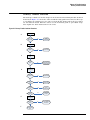
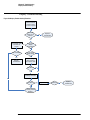
The main procedural tool in this chapter is the flowchart. The Primary Trouble Isolation
flowchart in Figure 4- 1 shows the entire troubleshooting path from a failed oscilloscope
to a working one, and directs you to other sections in this chapter where the procedures
are described in detail. Reference letters on the flowcharts point to procedural steps
that explain the brief instructions in the chart.
Figure 4-1 Primary Trouble Isolation Flowchart
$
3HUIRUP3RZHU8S
'RHVV\VWHP
VWD\RQ2."
1R
*RWR³3RZHU
6XSSO\
7URXEOHVKRRWLQJ´
1R
*RWR³'LVSOD\
7URXEOHVKRRWLQJ´
<HV
%
&KHFNGLVSOD\
,VGLVSOD\RQ
VFUHHQ"
<HV
&
5XQVFRSHVHOI
WHVWV
'RVHOIWHVWV
SDVV"
1R
*RWR³$FTXLVLWLRQ
%DFNSODQH$VVHPEO\
7URXEOHVKRRWLQJ´
<HV
'
5XQNH\ERDUGDQG
/('VHOIWHVWV
'RHVNH\ERDUG
ZRUN2."
1R
*RWR³.H\ERDUG
7URXEOHVKRRWLQJ´
1R
*RWR³/('
7URXEOHVKRRWLQJ´
'RHVWRXFK
VFUHHQZRUN
2."
1R
*RWR³7RXFK
6FUHHQ
7URXEOHVKRRWLQJ´
'RSUREHV
ZRUN2."
1R
*RWR³&KHFNLQJ
3UREH3RZHU
2XWSXWV´
<HV
'R/('VZRUN
2."
<HV
(
5XQDVHOIFDO
'RHVVHOIFDO
SDVV"
1R
*RWRSURFHGXUDOVWHS
³(6HOI&DOLEUDWLRQ´LQ
WKLVVHFWLRQ
<HV
)
6\VWHPZRUNV
5XQSHUIRUPDQFH
WHVWV
47
Chapter 4: Troubleshooting
Primary Trouble Isolation
A
Perform power-up.
Connect the oscilloscope power cord and press the power button in the lower left corner
of the front panel. If the oscilloscope is working properly, it will take several minutes
to start up. The LEDs on the front panel should all illuminate brightly for several
seconds, then dim. If the LEDs do not light up, refer to “LED Troubleshooting” later
in this chapter.
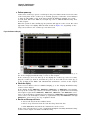
When the system is done starting up, the graticule will appear on the screen. The exact
appearance may look slightly different than shown in Figure 4- 2, depending on the
setup selected before the oscilloscope was turned off.
Figure 4-2 Power-on Display
If the oscilloscope turns off without you pressing the front panel power button, go to
the “Power Supply Troubleshooting” section of this chapter.
If the oscilloscope does not start up at all, unplug the oscilloscope, wait 30 seconds,
plug the oscilloscope back in, and turn the power on. If it still does not start up, go
to the “Setting Up the BIOS” and “Motherboard Verification” sections of this chapter.
B
Check the display.
If the screen is black or has a scrambled display, go to the “Display Troubleshooting”
section of this chapter.
If the display shows MEMCON1, MEMCON2, MEMCON3, or MEMCON4 errors during
boot- up of the oscilloscope software, the bottom (channel 1) acquisition board is faulty
and requires replacement. MEMCON5, MEMCON6, MEMCON7, and MEMCON8 errors
refer to the next higher acquisition board (channel 2). MEMCOM9 through MEMCON12
errors refer to the next higher (channel 3) acquisition board, and MEMCON13 through
MEMCON16 errors refer to the top acquisition board.
C
Run the oscilloscope self-tests.
1 Select Self Test from the Utilities menu.
2 Select Scope Self Test from the Self Test drop- down list box.
3 Click Start Test and follow the instructions on the screen.
If any of the self tests fail, go to the “Acquisition/Backplane Assembly Troubleshooting”
section of this chapter for further troubleshooting.
48
Chapter 4: Troubleshooting
Primary Trouble Isolation
D
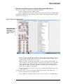
Check the front panel response by running the Keyboard and LED self tests.
Follow these steps to verify correct keyboard operation.
1 Select Self Test from the Utilities menu.
2 Select Keyboard Test from the Self Test drop- down list box, then click Start Test.
The Front Panel Keyboard Test window appears with a symbolic representation of the
keyboard. See Figure 4- 3.
Figure 4-3 Knob and key self test screen
When you press a key
or turn a knob in both
directions, the
corresponding symbol
on this screen turns
green.
3 Press each key on the keyboard until you have pressed all keys.When you press
a key or push a knob, the bar above the corresponding key/knob symbol on the
display should change from red to green.
4 Turn each knob in both directions until you have turned all knobs.When you
turn a knob in one direction, half the rotation arrow under the corresponding
knob symbol should turn green. When you then turn the knob in the other
direction, the entire rotation arrow under the knob symbol should turn green.
5 When you are finished, click Close.
6 If any of the knobs or keys do not work, go to “Keyboard Troubleshooting” later
in this chapter.
Follow these steps to test the front panel LED (light- emitting diode) indicators.
1 Select Self Test from the Utilities menu.
2 Select LED Test from the Self Test drop- down list box, then click Start Test.
49
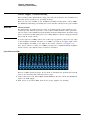
Chapter 4: Troubleshooting
Primary Trouble Isolation
The Front Panel LED Test screen appears, showing a symbolic representation of all
front panel LED indicators. See Figure 4- 4.
Figure 4-4 LED test screen
3 Repeatedly press the [Single] button on the front panel to step through and
highlight each LED symbol in the test screen. You can also step through the
LEDs by pressing the << Prev or Next >> buttons on the screen. Verify that the
corresponding LEDs on the front panel are the only ones illuminated.
Additionally, pressing the [Multi Purpose] button on the front panel will illuminate
all the LEDs, and pressing the [Clear Display] button on the front panel will turn
off all the LEDs.
4 When you are finished, click Close.
5 If any of the LEDs do not work, go to “LED Troubleshooting” later in this chapter.
6 If the touch screen is not working properly, go to the “Touch Screen
Troubleshooting” section of this chapter.
7 If the oscillator board is not working properly, go to “Oscillator Board
Troubleshooting” in this chapter.
8 To check power outputs of the probes, go to “Checking Probe Power Outputs”
in this chapter.
50
Chapter 4: Troubleshooting
Primary Trouble Isolation
E
Run a self calibration.
1 Complete a self calibration by following the procedures in chapter 2.
2 If the calibration test fails, look at the details to find the channel associated with
the failure.
• If the failure is associated with a RealEdge Technology channel, replace the two
acquisition boards associated with the RealEdge Technology.
• If replacing the two acquisition boards does not fix the problem with the RealEdge
Technology channels, replace the RealEdge Technology attenuators and modules.
• If the failure is associated with channel 1, look at the specific calibration that
failed. If it was a trigger cal, a time scale cal, or an interpolator gain cal, replace
the backplane board because it is likely the problem. If the cal still fails, replace
the bottom acquisition board.
• If the failure is associated with channel 1 but is not a trigger cal, a time scale
cal, or an interpolator gain cal, replace the bottom acquisition board. If the cal
still fails, replace the backplane board.
• If the failure is not associated with channel 1, replace the acquisition board
associated with that channel (channel 1 - bottom acquisition board, channel 2
- next higher acquisition board, channel 3 - next higher acquisition board,
channel 4 - top acquisition board).
• If all four channels have cal failures, the problem may be with the calibrator
located on the backplane board, so replace that board first. If the calibration
test passes, go to step F.
F The system is operational. Verify that the oscilloscope meets all warranted specifications
by following the procedures in the “Testing Performance” chapter.
51
Chapter 4: Troubleshooting
Power Supply Troubleshooting
Power Supply Troubleshooting
This section provides information to help you isolate the problem to the assembly level
when the power system is not operating properly.
There are two sets of LEDs on the backplane assembly. Seeing which of these LEDs
are illuminated will help you identify the reason and the remedy for the power failure.
WARNING
SHOCK HAZARD!
The maintenance described in this section is performed with power supplied to the
oscilloscope and with the protective covers removed. Only trained service personnel
who are aware of the hazards involved should perform the maintenance. Read the safety
notices at the back of this guide before proceeding. Failure to observe safety precautions
may result in electric shock.
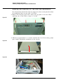
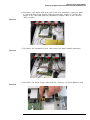
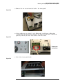
To locate both sets of LEDs, remove the oscilloscope top panel to expose the top edges
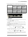
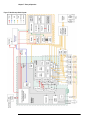
of the backplane assembly. The first set of LEDs is located in the upper right corner
of the backplane assembly, to the right of the J13001 connector (see Figure 4- 5).
Note: If you cannot see either set of LEDs, you may have a slightly modified backplane
board. Contact your Agilent Service Center for assistance.
Figure 4-5 First set of LEDs
This set of LEDs works in groups. To use them to determine the problem and remedy,
refer to the following table and follow these steps:
1 Connect the power cord. All 16 LEDs should illuminate. If none of them are illuminated,
replace the bulk supply.
2 Turn power on. If all 16 LEDs turn off, the power supplies are working.
52
Chapter 4: Troubleshooting
Power Supply Troubleshooting
PS01
ON
ON
ON
ON
PS02
ON
ON
ON
ON
LED
PS03
ON
ON
OFF
OFF
PS04
ON
OFF
ON
OFF
Type of Fault
Supply late
Supply late
Supply late
Supply late
ON
ON
ON
ON
OFF
OFF
OFF
OFF
ON
ON
OFF
OFF
ON
OFF
ON
OFF
Under-voltage
Under-voltage
Under-voltage
Under-voltage
OFF
OFF
OFF
OFF
OFF
OFF
OFF
OFF
OFF
ON
ON
ON
OFF
OFF
X
ON
OFF
ON
OFF
X
Over-voltage
Over-voltage
Over-voltage
Over-voltage
Power button pushed at wrong time
PS11
ON
ON
ON
ON
PS12
ON
ON
ON
ON
PS13
ON
ON
OFF
OFF
PS14
ON
OFF
ON
OFF
Supply late
Supply late
Supply late
Supply late
ON
ON
ON
ON
OFF
OFF
OFF
OFF
ON
ON
OFF
OFF
ON
OFF
ON
OFF
Under-voltage
Under-voltage
Under-voltage
Under-voltage
OFF
OFF
OFF
OFF
OFF
OFF
OFF
OFF
OFF
ON
ON
ON
OFF
OFF
X
ON
OFF
ON
OFF
X
Over-voltage
Over-voltage
Over-voltage
Over-voltage
Power button pushed at wrong time
PS21
ON
ON
ON
PS22
ON
ON
ON
PS23
ON
ON
OFF
PS24
ON
OFF
OFF
Supply late
Supply late
ON
ON
ON
OFF
OFF
OFF
ON
ON
OFF
ON
OFF
OFF
Under-voltage
OFF
OFF
OFF
OFF
ON
OFF
OFF
OFF
OFF
ON
ON
ON
OFF
OFF
OFF
ON
OFF
ON
OFF
ON
Over-voltage
Over-voltage
Acquisition power good is late
ON
OFF
OFF
ON
Acquisition power good went low
What To Do
Replace Backplane Assembly
Unplug scope, wait 30 seconds,
plug in, power up
Replace Backplane Assembly
Unplug scope, wait 30 seconds,
plug in, power up
Replace Backplane Assembly
Swap out each acquisition
board until problem is resolved
See AUV0, AUV1, AUV2, or
AUV3
53
Chapter 4: Troubleshooting
Power Supply Troubleshooting
PS71
ON
ON
ON
ON
PS72
ON
ON
ON
ON
LED
PS73
ON
ON
OFF
OFF
PS74
ON
OFF
ON
OFF
Type of Fault
Supply late
Supply late
Supply late
Supply late
ON
ON
ON
ON
OFF
OFF
OFF
OFF
ON
ON
OFF
OFF
ON
OFF
ON
OFF
Under-voltage
Under-voltage
Under-voltage
Under-voltage
OFF
OFF
OFF
OFF
OFF
OFF
OFF
OFF
OFF
ON
ON
ON
OFF
OFF
X
ON
OFF
ON
OFF
X
Over-voltage
Over-voltage
Over-voltage
Over-voltage
Power button pushed at wrong time
What To Do
Replace Backplane Assembly
Unplug scope, wait 30 seconds,
plug in, power up
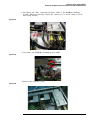
The second set of LEDs is located to the left of the first set and slightly lower, below
the J12002 connector (see Figure 4- 6).
Figure 4-6 Second set of LEDs
The following table shows each LED in this second set, the type of fault it indicates,
and what to do if that LED indicator is illuminated. When identifying which acquisition
assembly to replace, remember that the acquisition assembly nearest the bottom of the
oscilloscope is for channel 1. The one above it is for channel 2. The next higher is for
channel 3, and the top acquisition assembly is for channel 4.
NOTE
54
There is no correlation between the short name of each LED and the type of
fault. Use the table to determine the fault and how to address the problem.
Chapter 4: Troubleshooting
Power Supply Troubleshooting
LED
Type of Fault
What To Do
AOT0*
Over-temperature
Replace acquisition assembly 4
AOT1*
Over-temperature
Replace acquisition assembly 4
AOT2*
Over-temperature
Replace acquisition assembly 3
AOT3*
Over-temperature
Replace acquisition assembly 3
AOT4*
Over-temperature
Replace acquisition assembly 2
AOT5*
Over-temperature
Replace backplane assembly 2
AOT6*
Over-temperature
Replace backplane assembly 1
AOT7*
Over-temperature
Replace acquisition assembly 1
AOV0
Under-voltage
Replace acquisition assembly 4
AOV1
Under-voltage
Replace acquisition assembly 3
AOV2
Under-voltage
Replace acquisition assembly 2
AOV3
Under-voltage
Replace acquisition assembly 1
AUV0
Over-voltage
Replace acquisition assembly 4
AUV1
Over-voltage
Replace acquisition assembly 3
AUV2
Over-voltage
Replace acquisition assembly 2
AUV3
Over-voltage
Replace acquisition assembly 1
BOV0
Over-voltage
Replace assembly indicated by
illuminated AUV0 or FBS LED
BOV1
Used for internal testing
purposes only
N/A
BOV2
Any
Any problem that causes a
shutdown also turns on this LED
BOV3
Used for internal testing
purposes only
N/A
BOVG
Over-voltage
Replace backplane assembly
BSF
Over-voltage
Replace backplane assembly
FBS
Over-voltage
Replace backplane assembly
FLT
Over-voltage
Replace backplane assembly
*If an AOT LED is Lit
If the oscilloscope shuts down and the AOT0, AOT1, AOT2, AOT3, AOT4, AOT5, AOT6, or
AOT7 indicator LED is lit, then one of the scope channels is getting too hot or the
temperature sensing circuitry has failed. Normally, you would have to turn the
oscilloscope on and leave it on for awhile before you would see a shutdown caused by
temperature problems. If all the fans are turning, it is unlikely that the oscilloscope would
shut down due to temperature unless the airflow is being restricted or the input air is
already too hot to cool the insides of the oscilloscope.
It is possible that all the fans are working, but the oscilloscope still shuts down because
of temperature due to one or more of the channels malfunctioning and drawing too much
current. If so, you would need to replace the indicated acquisition assembly. It is also
possible for one of the heat sinks on one of the acquisition assemblies' critical parts to
become detached and cause that part to overheat and shut down the oscilloscope.
55
Chapter 4: Troubleshooting
Setting Up the BIOS
Setting Up the BIOS
If the BIOS settings become corrupt, the Infiniium oscilloscope PC motherboard will
not recognize the hard drive and the oscilloscope may not start. To configure the
motherboard BIOS parameters to the default settings, follow these steps:
1 Connect the power cable to the oscilloscope.
2 Connect the external keyboard to the rear panel.
3 Press Delete when the following prompt appears on the bottom of the screen:
Press TAB to show POST screen, DEL to Enter SETUP, F12 to Boot Menu.
If the prompt does not appear, or the oscilloscope does not appear to be functioning,
check the J12001 and J12002 motherboard power cable connectors. Otherwise, continue
with the next step.
4 Go to Load Optimal Defaults and press Enter for optimized values, or go to Load
Failsafe Defaults and press Enter for fail- safe values. Select OK to load the defaults,
then press Enter.
5 Go to the Save and Exit Setup option and press Enter to save and exit the setup.
Select Y to save and exit, then press Enter.
56
Chapter 4: Troubleshooting
Motherboard Verification
Motherboard Verification
If you have been through the Power Supply Troubleshooting section of this chapter and
the oscilloscope still does not stay powered up, the problem may be with the
motherboard. To diagnose this problem, follow these steps.
1 Remove the top panel.
2 Turn the oscilloscope on.
If the unit beeps once after about 5 to 10 seconds but fails to boot up, the motherboard
is defective and needs to be replaced.
If the unit fails to beep after it is powered on, then measure the potential relative to
the chassis at pin 9 of J12001 (Figure 4- 7). Pin 9 is the reset line for the motherboard.
It is controlled by the backplane. You should measure about 3.3V. If the potential you
measure is correct, but the unit still has not beeped and started up, the motherboard
is defective and needs to be replaced.
Figure 4-7 Measure potential relative to chassis at pin 9 of J12001
Pin 9 is located in
the bottom left corner
of J12001.
3 If the potential you measure is not correct, shut the oscilloscope down and unplug the
AC cord from the rear of the instrument.
4 Unplug the front panel power cable, the two large power cables that go to the
motherboard (J12001 and J12002), and the PCI Express cable (J10000) from the
backplane assembly. Do not allow the PCI Express cable to touch the backplane assembly
and cause a short circuit.
5 Plug the AC power back into the oscilloscope and turn the unit on if it does not come
on automatically.
6 Measure the potential relative to the chassis at pin 9 of J12001 again.
If you measure the required 3.3V, the motherboard is defective and needs to be replaced.
If you did not measure the correct voltage, the backplane assembly is defective and
must be replaced.
7 Be aware that there could be a fault on the motherboard that caused the backplane
assembly to fail so before you plug the motherboard cables back into the new backplane
assembly, measure the resistance to the chassis from the pin 9 contact in the connector
that plugs into J12001. If you measure a very low resistance or a short circuit to the
chassis, replace the motherboard and then assemble the instrument and confirm the
unit beeps and boots up properly.
57
Chapter 4: Troubleshooting
Display Troubleshooting
Display Troubleshooting
Figure 4-8 Display Troubleshooting Flowchart
&RQQHFWH[WHUQDO
PRQLWRUWR9*$
SRUW7XUQRQSRZHU
'RHVGLVSOD\
DSSHDURQH[W
PRQLWRU"
1R
5HSODFH
PRWKHUERDUG
<HV
&KHFNGLVSOD\FDEOH
<HV
FRQQHFWLRQWR
PRQLWRU
,VIURQWSDQHO
GLVSOD\
VFUDPEOHG"
1R
6WLOOVFUDPEOHG"
,VIURQWSDQHO
GLVSOD\EODFN"
<HV
<HV
5HSODFH
PRWKHUERDUG
&KHFNEDFNOLJKW
FDEOHDQGIURQW
SDQHOSRZHUFDEOH
6WLOOEODFN"
1R
1R
<HV
5HSODFHNH\ERDUG
DVVHPEO\UHDUERDUG
1R
6WLOOEODFN"
1R
'RQH*RWR
³3ULPDU\7URXEOH
,VRODWLRQ´
58
<HV
5HSODFH/&'
6WLOOEODFN"
<HV
5HSODFH
PRWKHUERDUG
Chapter 4: Troubleshooting
Display Troubleshooting
WARNING
INJURY CAN RESULT!
Use caution when the oscilloscope fan blades are exposed as they can cause injury.
Disconnect the power cable before working around the fans. Use extreme caution in
working with the oscilloscope when the cover is removed. If the procedure requires
you to have the cover off, be careful not to let these fan blades come in contact with
any part of your body.
For information on how to replace the display parts, see the "Replacing Assemblies"
chapter.
59
Chapter 4: Troubleshooting
Acquisition/Backplane Assembly Troubleshooting
Acquisition/Backplane Assembly Troubleshooting
This section describes which board assembly to replace if any of the scope self tests
fail. When the self- test error message file is generated it is sent to the following location:
C:\ProgramData\Agilent\Infiniium\selftest\SelfTestLog.txt
The error message usually indicates the channel with the error. When identifying which
acquisition assembly to replace, remember that the acquisition assembly nearest the
bottom of the oscilloscope is for channel 1. The one above it is for channel 2. The next
higher is for channel 3, and the top acquisition assembly is for channel 4. Replace the
acquisition assembly that has the error.
If the error message does not indicate a channel, refer to the following table to determine
which assembly to replace.
Test Group and Test Name
Error Type
Assembly to Replace
Timebase Test Group
Timebase Interpolator Test
Backplane assembly
ADC Test Group
ADC Register Tests
ADC Voltage Test Points
ADC1, ADC2, ADC3, ADC4
Acquisition assembly 1
ADC5, ADC6, ADC7, ADC8
Acquisition assembly 2
ADC9, ADC10, ADC11, ADC12
Acquisition assembly 3
ADC13, ADC14, ADC15, ADC16
Acquisition assembly 4
ADC1, ADC2, ADC3, ADC4
Acquisition assembly 1
ADC5, ADC6, ADC7, ADC8
Acquisition assembly 2
ADC9, ADC10, ADC11, ADC12
Acquisition assembly 3
ADC13, ADC14, ADC15, ADC16
Acquisition assembly 4
Hedwig0, Hedwig1, Hedwig2, Hedwig3, Oak0
Acquisition assembly 1
Hedwig4, Hedwig5, Hedwig6, Hedwig7, Oak2
Acquisition assembly 2
Pred1, Pred2, MainFPGA, Wahoo, Ambient
Backplane assembly
Merwig0, Merwig1
Replace acquisition assembly 1.
If error still occurs, put original
acquisition assembly back into
scope and replace backplane
assembly.
Merwig2, Merwig3
Replace acquisition assembly 2.
If error still occurs, put original
acquisition assembly back into
scope and replace backplane
assembly.
Merwig4, Merwig5, Hedwig8, Hedwig9,
Hedwig10, Hedwig11, Oak4
Replace acquisition assembly 3.
If error still occurs, put original
acquisition assembly back into
scope and replace backplane
assembly.
Misc. Scope Test Group
Temp Sensor Tests
60
Chapter 4: Troubleshooting
Acquisition/Backplane Assembly Troubleshooting
Test Group and Test Name
Acq Flash RAM Tests
Error Type
Assembly to Replace
Merwig6, Merwig7, Hedwig12, Hedwig13,
Hedwig14, Hedwig15, Oak6
Replace acquisition assembly 4.
If error still occurs, put original
acquisition assembly back into
scope and replace backplane
assembly.
Test is currently not being run.
61
Chapter 4: Troubleshooting
Keyboard Troubleshooting
Keyboard Troubleshooting
If some of the knobs fail the keyboard self test but some work properly, replace the
rear board of the keyboard assembly.
If none of the knobs work properly, replace the front board of the keyboard assembly.
If any of the keys do not work properly but the LEDs light up, replace the front board
of the keyboard assembly.
If the keys still do not work properly, check the incoming cables.
62
Chapter 4: Troubleshooting
LED Troubleshooting
LED Troubleshooting
LED Failure During System Start- Up
When power is turned on to the scope, the front panel LEDs should all illuminate
brightly for several seconds, then dim. The RealEdge LED (on 50 and 62 GHz models)
should pulse off and on. When the Infiniium software starts up, the LEDs should turn
off. If the LEDs do not light up this way during system start- up, then follow these steps:
1 Make sure connectors J2 and J3 on the front and rear boards of the keyboard assembly
are securely connected to their mates on the other board.
2 Ensure the power cable is properly connected.
3 Make sure J17 is connected on the rear board of the keyboard assembly.
On/Off Switch Backlight LED Failure During Self Test
If the on/off switch backlight LED is not working, check the on/off cable connecting
the On/Off board to the motherboard. If the LED still does not work, replace the On/Off
board. If the LED still does not illuminate, replace the motherboard.
Front Panel LED Failures During Self Test
If any of the other LEDs on the front panel are not working, check these cables:
• The power cable to the front panel
• The USB cable to the front panel
• The backlight connector (J1) to the motherboard
If the cables are connected and working properly but the LEDs are still not working,
then troubleshoot the acquisition assemblies to make sure they are working. If they are,
replace the front board of the keyboard assembly. If the LEDs still do not illuminate,
reload the oscilloscope software.
Replace the front board of the keyboard assembly in these cases:
• Only some of the LEDs illuminate
• No LEDs and no knobs work
• The knobs work but the LEDs don’t illuminate.
When reassembling the oscilloscope, be sure to reinstall all boards that were replaced,
but that were not causing the problem.
63
Chapter 4: Troubleshooting
Touch Screen Troubleshooting
Touch Screen Troubleshooting
Figure 4-9 Touch screen flowchart
'RHVWKHWRXFK
VFUHHQZRUN"
<HV
'RQH
<HV
,VWKHGULYHU
LQVWDOOHG"
1R
%
$
,VWKH7RXFK
EXWWRQOLW"
1R
1R
7XUQRQ7RXFK
EXWWRQ
7HVW86%SRUWZLWK
PRXVH
5HSODFHUHDUERDUG
RINH\ERDUG
DVVHPEO\DQGFKHFN
FDEOHFRQQHFWLRQV
<HV
<HV
&DOLEUDWHWKHWRXFK
VFUHHQ
'RFDOWHVWV
SDVV"
1R
5HSODFHWRXFK
VFUHHQ
'RHV86%SRUW
ZRUN2."
<HV
1R
5HSODFH
PRWKHUERDUG
'RHVWRXFK
VFUHHQZRUN
2."
<HV
'RQH
A To find the driver, bring up the Start menu, right click Computer, then go to Manage
> Device Manager > Human Interface devices and look for USB HID Touch Screen
Controller. To ensure that it is enabled and working properly, right click the file name
and select Properties. The General tab in the Properties menu should display a message
stating that the device is working properly.
B To calibrate the touch screen, go to All Programs > Microchip TSHARC Control Panel.
Select the Calibration tab, then press Begin Calibration and follow the instructions.
64
Chapter 4: Troubleshooting
Oscillator Board Troubleshooting
Oscillator Board Troubleshooting
If you encounter any problems with the oscillator board, first check all cabling and
connections to ensure they are secure and tight:
• Check the connection between the oscillator board and the backplane board.
• Check the 10 GHz DRO output cable.
• Check the reference to the oscillator board cable.
• Check the 32 GHz DRO power cable (50 and 62 GHz models).
• Check the 32 GHz DRO cable connected to the RealEdge modules and the RealEdge
auxiliary module (50 and 62 GHz models).
• Check the coax cables between the RealEdge auxiliary module and the RealEdge
modules (50 and 62 GHz models).
If you cannot calibrate the time scale, or if all channels have excessive sample clock
jitter, then replace the oscillator board.
If you get an error message similar to the following example, tighten the cable connections
from the oscillator board to the RealEdge inputs. If the error appears again, replace
the oscillator board:
Self calibration failure on Channel 1R, pilot tone amplitude too small
If replacing the oscillator board does not fix the problem, then replace the backplane
board.
You must run a user calibration after replacing an oscillator board.
65
Chapter 4: Troubleshooting
Checking Probe Power Outputs
Checking Probe Power Outputs
Probe power outputs are on the front panel, in the lower left corner of the 3.5mm inputs.
Refer to Figure to check the power output at the connectors. Measure the voltages
with respect to the ground terminal on the front panel, located near Aux Out. Measure
the voltages at pins 2 and 5 only (+12V and - 12V). These supplies, and all others, come
from the front panel.
Figure 4-10 AutoProbe II pins
66
Chapter 4: Troubleshooting
Before You Contact Agilent
Before You Contact Agilent
If you have read this Troubleshooting chapter and have unresolved questions about
troubleshooting the oscilloscope, be ready to provide system information such as the
current software version and installed options. This information will be useful when
you contact Agilent Technologies.
To find and save system information, follow these steps:
1 Select Help > About Infiniium.
A dialog box similar to the one in Figure 4- 11 appears.
Figure 4-11 About Infiniium Information
2 Click Copy To Clipboard.
3 Bring up a text editor, such as Notepad, and paste the copied information into the editor.
4 Save the text editor file.
67
Chapter 4: Troubleshooting
Before You Contact Agilent
68
5
ESD Precautions 70
Tools Required 70
Returning the Oscilloscope to Agilent Technologies for Service 71
Removing and Replacing the Top Panel and Motherboard 72
Removing and Replacing the Hard Disk Drive 77
Removing and Replacing the Power Supply 78
Removing and Replacing the Front Panel Assembly and Bottom Panel 79
Removing and Replacing Front Panel Assembly Parts 86
Removing and Replacing RealEdge Components 91
Removing and Replacing the Acquisition Boards/Backplane Assembly 94
Setting the Calibration Factors after Replacing an Acquisition Board 101
Removing and Replacing the Fans 102
Removing and Replacing the USB Controller Cable 104
Replacing Assemblies
Replacing Assemblies
Use the procedures in this chapter when removing and replacing assemblies and parts
in the Agilent Technologies oscilloscopes.
In general, the procedures that follow are placed in the order to be used to remove a
particular assembly. The procedures listed first are for assemblies that must be removed
first.
The graphics in this chapter are representative of the oscilloscope at the time of this
printing. Your unit may look different.
ESD Precautions
When using any of the procedures in this chapter you must use proper ESD precautions.
As a minimum you must place the oscilloscope on a properly grounded ESD mat and
wear a properly grounded ESD wrist strap.
CAUTION
AVOID DAMAGE TO THE OSCILLOSCOPE!
Failure to implement proper antistatic measures may result in damage to the oscilloscope.
Tools Required
The following tools are required for these procedures.
•
•
•
•
•
•
•
•
•
Torx drivers: T10, T20
Socket wrench: 5/8 inch
Torque wrench: 5/16 inch (8 in- lbs)
Flat- blade screwdriver: medium size (3/16 inch)
Power driver vertical with T- 20 bit (18 in- lbs)
Power driver vertical with T- 10 bit (5 in- lbs)
Hex socket bit: 5/16 inch
Open- end wrench: size 6 metric
Needle- nose pliers (optional)
CAUTION
REMOVE POWER BEFORE REMOVING OR REPLACING ASSEMBLIES!
Do not remove or replace any circuit board assemblies in this oscilloscope while power
is applied. The assemblies contain components which may be damaged if the assembly
is removed or replaced while power is connected to the oscilloscope.
WARNING
SHOCK HAZARD!
To avoid electrical shock, adhere closely to the following procedures. Also, after
disconnecting the power cable, wait at least three minutes for the capacitors on the
power supply to discharge before servicing this oscilloscope. Hazardous voltages exist
on the inverter for the display monitor.
WARNING
SHOCK HAZARD!
Read the Safety information at the back of this guide before performing the following
procedures. Failure to observe safety precautions may result in electrical shock.
WARNING
INJURY CAN RESULT!
Use caution when the oscilloscope fan blades are exposed as they can cause injury.
70
Chapter 5: Replacing Assemblies
Returning the Oscilloscope to Agilent Technologies for Service
Returning the Oscilloscope to Agilent Technologies for Service
Before shipping the oscilloscope, contact Agilent Technologies, Inc. for more
details.
1 Write the following information on a tag and attach it to the oscilloscope.
• Name and address of owner
• Oscilloscope model numbers
• Oscilloscope serial numbers
• Description of the service required or failure indications
2 Remove all accessories from the oscilloscope.
3
4
5
6
Accessories include all cables. Do not include accessories unless they are
associated with the failure symptoms.
Protect the oscilloscope by wrapping it in plastic or heavy paper.
Pack the oscilloscope in foam or other shock- absorbing material and place it
in a strong shipping container.
You can use the original shipping materials or order materials from an Agilent
Technologies Sales Office. If neither is available, place 16 to 20 cm (6 to 8
inches) of shock- absorbing material around the oscilloscope and place it in a
box that does not allow movement during shipping.
Seal the shipping container securely.
Mark the shipping container as FRAGILE.
In any correspondence, refer to the oscilloscope by model number and full serial
number.
71
Chapter 5: Replacing Assemblies
Removing and Replacing the Top Panel and Motherboard
Removing and Replacing the Top Panel and Motherboard
Note that all sheet metal holes that are supposed to have screws placed in them
are marked by lines on four sides of the hole.
1 Remove the four M3 screws that connect the top panel to the rear. When
replacing, use a Torx T10 to torque to 5 in- lbs.
Figure 5-1
2 Slide the top panel back 1 to 2 inches and then lift it off. If necessary, gently
pry it using a flat- blade screwdriver at the rear lip.
Figure 5-2
Figure 5-3
72
Chapter 5: Replacing Assemblies
Removing and Replacing the Top Panel and Motherboard
3 Disconnect the PCIe cable by pressing down on the locking tab and pulling the
cable.
Figure 5-4
4 Disconnect the red SATA cable.
Figure 5-5
5 Disconnect the display cable (left circle in photo) and the standby switch cable
(right circle, next to the SATA cable).
Figure 5-6
73
Chapter 5: Replacing Assemblies
Removing and Replacing the Top Panel and Motherboard
6 Disconnect the two USB cables.
Figure 5-7
7 Disconnect the power cable from the four locations shown in the next three
figures.
Figure 5-8
Figure 5-9
74
Chapter 5: Replacing Assemblies
Removing and Replacing the Top Panel and Motherboard
Figure 5-10
8 If you need to replace the motherboard fan, disconnect the cable from the fan
to the motherboard now. Otherwise, you do not need to disconnect it.
Figure 5-11
9 Disconnect the USB controller cable.
Figure 5-12
75
Chapter 5: Replacing Assemblies
Removing and Replacing the Top Panel and Motherboard
10 Remove the PCIe cable from the motherboard and set it aside to put on the
new motherboard.
11 Remove the six M3 screws from the motherboard. When replacing, torque the
screws to 5 in- lbs.
Figure 5-13
12 Pull the motherboard away from the back panel and then lift it out. Place the
motherboard in an anti- static bag.
13 To reassemble the motherboard, reverse the above procedure. You will need a
new heat sink and bracket and a support assembly board (54904- 41203) when
putting in a new motherboard.
Figure 5-14
76
Chapter 5: Replacing Assemblies
Removing and Replacing the Hard Disk Drive
Removing and Replacing the Hard Disk Drive
1 Loosen the two screws on back of the hard disk drive.
Figure 5-15
2 Pull the hard drive out.
Figure 5-16
3 Remove the four screws connecting the disk drive to the bottom of the plate.
4 To replace the hard disk drive, reverse this procedure.
77
Chapter 5: Replacing Assemblies
Removing and Replacing the Power Supply
Removing and Replacing the Power Supply
WARNING
SHOCK HAZARD!
If the power supply is defective it could have a dangerous charge on some
capacitors. This charge could remain for many days after removing power from
the supply.
1 Loosen the rear panel screw and lower the handle.
Figure 5-17
2 Remove the power supply.
3 Reverse the procedure to replace the power supply.
78
Chapter 5: Replacing Assemblies
Removing and Replacing the Front Panel Assembly and Bottom Panel
Removing and Replacing the Front Panel Assembly and Bottom
Panel
1 Remove the top panel as described previously. Disconnect the two USB cables
and the display and standby switch cables as described previously. Unsnap the
locking clip to remove the USB cable. Also disconnect the front panel power
cable from the backplane board.
Figure 5-18
2 Remove the four screws (two on each side) connecting the front panel assembly
to the top of the chassis.
Figure 5-19
79
Chapter 5: Replacing Assemblies
Removing and Replacing the Front Panel Assembly and Bottom Panel
3 Turn the oscilloscope upside- down and remove the four M3 screws connecting
the bottom panel to the back panel. When replacing, torque the screws to 5 in- lbs.
Figure 5-20
4 Remove the five M3 screws from the bottom panel.
Figure 5-21
5 Remove the bottom panel.
80
Chapter 5: Replacing Assemblies
Removing and Replacing the Front Panel Assembly and Bottom Panel
6 Disconnect each input cable from each of the four attenuator connectors using
a 5/16- inch Hex torque wrench. When reconnecting, torque to 8 in- lbs. The
length of the cable will guide the installation (longest cable on left, shortest
cable on right).
Figure 5-22
7 Disconnect the attenuator power cable from each input channel attenuator.
Figure 5-23
8 Disconnect the Probe Comp cable from the connector on the backplane board.
Figure 5-24
81
Chapter 5: Replacing Assemblies
Removing and Replacing the Front Panel Assembly and Bottom Panel
9 Disconnect the Aux Out and Cal Out cables from both the front panel and the
backplane board. Pull straight back to remove the cables from the backplane
board. CAUTION: Be sure to pull straight back to avoid bending or breaking
the connection to the backplane board. When reconnecting, gently reinsert each
cable. You will hear a snap when it is fully seated.
Figure 5-25
Figure 5-26
The front panel is now disconnected.
Removing a RealEdge Assembly
If you are working on a 50 or 62 GHz model, it will have a RealEdge assembly.
The following steps show how to remove it. Be sure to remove the RealEdge
assembly before removing the front panel to avoid damaging the assembly.
1 Disconnect the two input cables from the RealEdge modules and from the
RealEdge modules to the RealEdge auxiliary module.
Figure 5-27
82
Chapter 5: Replacing Assemblies
Removing and Replacing the Front Panel Assembly and Bottom Panel
2 Disconnect the cable connecting the pilot cables to the RealEdge auxiliary
module. When reconnecting, torque the connectors to 8 in- lbs. using a 5/8- in.
hex torque wrench.
Figure 5-28
3 Disconnect the RealEdge assembly power cables.
Figure 5-29
4 Remove the four M3 screws.
Figure 5-30
83
Chapter 5: Replacing Assemblies
Removing and Replacing the Front Panel Assembly and Bottom Panel
5 Gently remove the RealEdge assembly, keeping the cables from getting caught.
Gently slide it toward the back, careful to avoid catching any parts on the sheet
metal flange on the chassis.
Figure 5-31
6 Flip the RealEdge assembly over and disconnect the remaining cables: two input
cables, two attenuator cables, and the two cables coming from the 32 GHz DRO.
You do not need to disconnect the cables from the DRO itself.
Figure 5-32
7 Place the RealEdge assembly into an anti- static bag.
84
Chapter 5: Replacing Assemblies
Removing and Replacing the Front Panel Assembly and Bottom Panel
Finishing Removal of the Front Panel
1 To finish removing the front panel, remove the four M3 screws (two on each
side) connecting the front panel to the bottom of the chassis. When replacing,
torque the screws to 5 in- lbs.
Figure 5-33
2 Pull off the front panel, carefully feeding the USB cable through the opening.
3 To replace the front panel assembly, reverse this procedure.
85
Chapter 5: Replacing Assemblies
Removing and Replacing Front Panel Assembly Parts
Removing and Replacing Front Panel Assembly Parts
Remove the front panel assembly as described in the previous section.
Front Panel Clutches, Connectors, and Knobs
WARNING
This step will ruin the clutch. You will have to replace the clutch with a new one.
1 Use a thin item such as a ribbon to protect the oscilloscope from scratches,
and pull on the dark gray plastic clutches to pop them off of the oscilloscope.
2 Use your fingers to pull off the knobs.
Front Panel Bezel and Front Panel Assembly
1 Remove the seven M3 screws (three from each side and one from the bottom).
When replacing the screws, torque to 5 in- lbs.
Figure 5-34
2 Disconnect the orange touch screen cable.
Figure 5-35
86
Chapter 5: Replacing Assemblies
Removing and Replacing Front Panel Assembly Parts
3 Remove the six screws from the back of the front panel.
Figure 5-36
4 If the oscilloscope is a 20, 25, or 32 GHz model, it will have a filler plate
covering Trig Out and Aux Trig. Remove this plate from the back of the front
panel by removing the nuts and washers from the cables.
Figure 5-37
Remove nuts
and washers
5 Lift off the front panel bezel.
Figure 5-38
87
Chapter 5: Replacing Assemblies
Removing and Replacing Front Panel Assembly Parts
6 The front circuit board of the keyboard assembly is connected to the front bezel.
If you need to remove and replace only this front board, push the snap tabs
out of way with a screwdriver and pull out the board.
7 Disconnect the autoprobe cable and backlight cable.
Figure 5-39
8 Remove the two M3 screws, top right and bottom left, connecting the rear board
of the keyboard assembly to the deck, and remove the board. When reinstalling,
torque to 5 in- lbs.
Figure 5-40
9 To reassemble the front panel assembly, reverse these steps.
88
Chapter 5: Replacing Assemblies
Removing and Replacing Front Panel Assembly Parts
Cal Connector (Power Button) Assembly
1 Remove the two screws connecting the cal bracket to the front deck. When
replacing, use a power driver and T- 10 bit to torque the screws to 8 in- lbs.
Figure 5-41
2 Remove the cal connector assembly from the front panel deck. Carefully pull
the cables through the front deck. Replace individual parts as needed.
Figure 5-42
Display Assembly
1 Remove the front panel bezel and front panel assembly as described previously.
2 Disconnect the display cable from the back of the display.
Figure 5-43
89
Chapter 5: Replacing Assemblies
Removing and Replacing Front Panel Assembly Parts
3 Remove the four M3 screws (two on each side) connecting the display to the
deck. When reinstalling, torque to 5 in- lbs.
Figure 5-44
Attenuators (20, 25, and 33 GHz Models)
1 Remove the four screws connecting each attenuator to its bracket. When
reconnecting, torque the screws to 8 in- lbs.
2 Remove the four attenuators by removing the nut of the attenuator from the
threads of the 3.5 mm connector. Remove the attenuator from the bracket. When
replacing, use a hand torque wrench to torque the nuts to 8 in- lbs.
Figure 5-45
90
Chapter 5: Replacing Assemblies
Removing and Replacing RealEdge Components
Removing and Replacing RealEdge Components
This section describes how to remove and replace the RealEdge modules and
the attenuator components of the RealEdge assembly.
1 Remove the RealEdge assembly as described previously.
2 Remove the two screws from the back of the top RealEdge module as shown
below. When replacing, torque to 5 in- lbs.
Figure 5-46
3 Loosen the connection between the RealEdge SMA connector and the attenuator
connector. Be careful to handle the RealEdge module by the casing and not the
connector. When tightening, torque the connector to 8 in- lbs.
Figure 5-47
91
Chapter 5: Replacing Assemblies
Removing and Replacing RealEdge Components
4 Carefully remove the RealEdge module.
Figure 5-48
5 Remove the two screws on the side of the attenuator. When replacing, torque
to 5 in- lbs.
Figure 5-49
6 Loosen the SMA connector from the male SMA connector on the 1.85 connector.
When replacing, torque the connector to 8 in- lbs.
Figure 5-50
7 Remove the attenuator assembly.
92
Chapter 5: Replacing Assemblies
Removing and Replacing RealEdge Components
8 Remove the two screws connecting the attenuator to the bracket. When replacing,
hand tighten the screws and then back off the screw one full turn to allow the
frame to move. Tighten the screws after the connector is tightened.
Figure 5-51
9 Repeat these steps to remove and replace the bottom RealEdge module and
attenuator.
93
Chapter 5: Replacing Assemblies
Removing and Replacing the Acquisition Boards/Backplane Assembly
Removing and Replacing the Acquisition Boards/Backplane
Assembly
Use these procedures to remove and replace the acquisition and backplane
assemblies and individual acquisition boards. When necessary, refer to other
removal procedures. The graphics in this chapter are representative of the
oscilloscope at the time of this printing. Your unit may look different.
Removing the acquisition and backplane assemblies
1 Remove the top panel, power supply, front panel assembly, and bottom panel
as described previously.
2 Remove all cables connected to the backplane board.
Figure 5-52
3 Remove the two M4 screws from the backplane tray (one in each corner).
Figure 5-53
4 Turn the oscilloscope over.
94
Chapter 5: Replacing Assemblies
Removing and Replacing the Acquisition Boards/Backplane Assembly
5 Disconnect the cables from the rear panel (four cables for 33 GHz and lower
models; six cables for 50 GHz and 62 GHz models), using 5/8 (left photo) and
5/16 (right photo) drivers. When reconnecting, torque the nut and washers to
18 in- lbs.
Figure 5-54
6 If you need to replace the oscillator board, remove the four M3 screws connecting
the board to its tray and disconnect all attached cables. When replacing, torque
the screws to 5 in- lbs and torque SMA connectors to 8 in- lbs using a 5/16inch hand torque wrench.
Figure 5-55
7 Remove the two screws connecting the backplane deck to the chassis.
Figure 5-56
95
Chapter 5: Replacing Assemblies
Removing and Replacing the Acquisition Boards/Backplane Assembly
8 Remove the four M4 screws from the rear panel of the chassis. When replacing,
torque the screws to 18 in- lbs.
Figure 5-57
9 Dress all cables into the center to keep them from getting caught.
10 Lift the entire backplane board/acquisition assembly out of the chassis and
place it on another table. Use the handles, as the assembly is heavy.
Figure 5-58
96
Chapter 5: Replacing Assemblies
Removing and Replacing the Acquisition Boards/Backplane Assembly
Removing an Acquisition Board
When removing an individual acquisition board, keep in mind that acquisition
board 1 is next to the oscillator board and it has the longest cable. Acquisition
board 4 has the shortest cable. You may want to label the acquisition boards
1 through 4 for easy reference.
1 Carefully remove the five clock cables from the DRO to the acquisition boards
using a 5/16 Torx wrench. Be sure to avoid catching the cables on any acquisition
board components.
Figure 5-59
2 Remove the attenuator control cables.
Figure 5-60
97
Chapter 5: Replacing Assemblies
Removing and Replacing the Acquisition Boards/Backplane Assembly
3 Remove the 10 M4 screws (five from each side) connecting the acquisition boards
to the rear panel. Keep the oscillator board tray connected to acquisition board
1 unless you have already removed it. When reassembling, torque the screws
to 18 in- lbs using a T20 driver.
Figure 5-61
4 Lift off the rear panel.
5 Remove the two screws (one on each side) connecting the oscillator board tray
to the backplane deck, unless you are replacing only acquisition board 4.
Figure 5-62
To remove only board 4, disconnect the 54932- 61624 cable and the attenuator
cable connection from board 4 only. Then remove the cable from the backplane
board to the DRO.
6 Lift the oscillator board tray straight up and slide it forward, carefully threading
the input cables through the opening. Place the oscillator board into an antistatic bag.
98
Chapter 5: Replacing Assemblies
Removing and Replacing the Acquisition Boards/Backplane Assembly
7 Remove the eight remaining screws securing the acquisition trays to the
backplane tray. Remove each acquisition board starting with the lowest slot
(next to the oscillator board).
Figure 5-63
8 Gently rock the acquisition board and guide the input cables through. Remove
the acquisition board and place it upside- down in an anti- static bag to avoid
crimping the cables.
9 Repeat steps 7- 8 for any additional acquisition boards to be removed, if
applicable. When removing the last acquisition board, grip it firmly and then
gently rock it up and out.
Removing Acquisition Board Cables and Trays
1 Disconnect the input cables (one cable for 20, 25, and 32 GHz models; two
cables for 50 and 62 GHz models) and feed them through the hole.
Figure 5-64
2 Remove the 10 screws connecting the acquisition board to the tray. Keep the
cables to attach to the new acquisition board.
99
Chapter 5: Replacing Assemblies
Removing and Replacing the Acquisition Boards/Backplane Assembly
Removing the Backplane Board from the Deck
1 Loosen the five guide pins. When replacing, torque the guide pins to 5 in- lbs
using a size 6 metric open- end wrench.
Figure 5-65
2 Using a T10 Torx, remove the 10 tie- down screws from the edges. When replacing,
torque the screws to 5 in- lbs.
Figure 5-66
3 Lift the backplane assembly off the deck.
100
Chapter 5: Replacing Assemblies
Setting the Calibration Factors after Replacing an Acquisition Board
Setting the Calibration Factors after Replacing an Acquisition
Board
You must perform a user calibration and self test procedure after replacing an
acquisition board. Refer to the calibration chapter in this Service Guide for
details.
Let the oscilloscope warm up before testing.
The oscilloscope under test must be warmed up (with the oscilloscope application running) for at least
30 minutes prior to the start of any performance test.
101
Chapter 5: Replacing Assemblies
Removing and Replacing the Fans
Removing and Replacing the Fans
WARNING
AVOID INJURY!
The fan blades are exposed both inside and outside the chassis. Disconnect the power
cable before working around the fan. Use extreme caution in working with the
oscilloscope. Failure to observe these precautions may result in injury.
1 Disconnect the power cable and remove the top panel, power supply, front
panel, bottom panel, and acquisition assembly as described earlier.
2 Remove the six M3 screws connecting the fan bracket to the chassis. When
replacing, torque the screws to 5 in- lbs.
Figure 5-67
3 Remove the fan assembly, carefully feeding the fan assembly cable through the
bottom of the chassis.
Figure 5-68
102
Chapter 5: Replacing Assemblies
Removing and Replacing the Fans
4 Clip off the end of each of the fan mounts (see Figure 5- 69) and take the fan
out. Repeat for each fan that needs to be replaced.
Figure 5-69
CAUTION
AVOID OVERHEATING THE OSCILLOSCOPE
When replacing the fan, be sure the direction of the fan air flow is coming from the
inside to the outside of the oscilloscope. Check the flow arrows on the fan and check
for proper flow once power is applied to the oscilloscope. Improper air flow can overheat
the oscilloscope.
5 To install the fan, reverse this procedure.
103
Chapter 5: Replacing Assemblies
Removing and Replacing the USB Controller Cable
Removing and Replacing the USB Controller Cable
1 Remove the top panel.
2 Remove the two self- tapping screws from the top edge of chassis. When replacing,
torque the screws to 3 in- lbs.
Figure 5-70
3 Disconnect both ends of the cable.
Figure 5-71
104
Chapter 5: Replacing Assemblies
Removing and Replacing the USB Controller Cable
4 Pull the connector cable out of the oscilloscope.
Figure 5-72
5 To replace the USB controller cable, reverse the procedure. Be careful not to
overtighten the screws.
105
Chapter 5: Replacing Assemblies
Removing and Replacing the USB Controller Cable
106
6
Ordering Replaceable Parts 108
Listed Parts 108
Unlisted Parts 108
Direct Mail Order System 108
Exchange Assemblies 108
Exploded Views 109
Replaceable Parts List 114
Replaceable Parts
Replaceable Parts
This chapter describes how to order replaceable assemblies and parts for the Agilent
90000 Q- Series oscilloscopes. Service support for this oscilloscope is replacement of
parts to the assembly level.
Ordering Replaceable Parts
Listed Parts
To order a part in the parts list, quote the Agilent Technologies part number, indicate
the quantity desired, and address the order to the nearest Agilent Technologies Sales
Office.
Unlisted Parts
To order a part not listed in the parts list, include the oscilloscope part number,
oscilloscope serial number, a description of the part (including its function), and the
number of parts required. Address the order to the nearest Agilent Technologies Sales
Office.
Direct Mail Order System
Within the USA, Agilent Technologies can supply parts through a direct mail order
system. There are several advantages to this system:
• Direct ordering and shipping from the Agilent Technologies parts center in California,
USA.
• No maximum or minimum on any mail order. (There is a minimum amount for parts
ordered through a local Agilent Technologies Sales Office when the orders require
billing and invoicing.)
• Prepaid transportation. (There is a small handling charge for each order.)
• No invoices.
For Agilent Technologies to provide these advantages, please send a check or money
order with each order.
Mail order forms and specific ordering information are available through your local
Agilent Technologies Sales Office. Addresses and telephone numbers are located in a
separate document shipped with the manuals.
Exchange Assemblies
Exchange assemblies have been set up for Agilent Service Center use only.
108
Chapter 6: Replaceable Parts
Exploded Views
Exploded Views
Front Panel
109
Chapter 6: Replaceable Parts
Exploded Views
Fan and Acquisition Assembly
110
Chapter 6: Replaceable Parts
Exploded Views
Oscillator Assembly
111
Chapter 6: Replaceable Parts
Exploded Views
Power Supply and PC Motherboard
112
Chapter 6: Replaceable Parts
Exploded Views
External
113
Chapter 6: Replaceable Parts
Replaceable Parts List
Replaceable Parts List
The following table is a list of replaceable parts. The information given for each part
consists of the following:
• Reference designation.
• Agilent Technologies part number.
• Total quantity (QTY) in oscilloscope or on assembly. The total quantity is given once
and at the first appearance of the part number in the list.
• Description of the part.
Replaceable Parts
Ref.
Des.
Agilent Part
Number
QTY
Description
A1
5062-1247
1
Assembly - 3.5 mm Connector
A2
54916-66414
1
PCA Autoprobe Board
A3
54932-66404
1
PCA Keyboard - Front
A4
54932-66405
1
PCA Keyboard
A5
2090-0993
1
Display-Touch Screen 15-in 330.08X254.9X2.25mm 8-wire resistive
A6
54932-66406
1
PCA On/Off Board
A7
08673-67601
1
Connector Assembly - Output
A8
2090-1012
1
Display LCD 15-in TFT 1024X768-Pixels 253.5-LG X 326.5-WD X11.5-D-mm
A9
33325-60019
1
Step attenuator, 35dB, 5V, Female-Male, Pb free
A10
54916-66701
1
Acquisition board tested
A11
54932-66502
1
Backplane Board Tested
A12
54932-68716
1
Fan with Fan Mounts - replacement
A13
54932-00102
1
Chassis
A14
54932-63401
1
Oscillator Assembly 10 GHz
A15
54932-63402
1
Oscillator Assembly 32 GHz
A16
5087-7351
1
Top Assembly, Hwin
A17
54932-66411
1
Oscillator Board
A18
5087-7361
1
Top Assembly, Pearl
A19
84905-60003
1
Attenuator 35DB,5 Volt, Female-Male, 67Ghz, Pb Free
A20
5064-7891
1
Conn 1.85 blkhd
A21
0950-5393
1
Power Supply 1600W single output 12V
A22
54932-83501
1
Infiniium 90000 Q-Series Imaged Hard Drive (Service Centers Only)
A22
54932-68717
1
Replacement HDD for m890/Win7-based DSO90000 Q-series scopes
A23
0960-2869
1
Mother Board Printed Circuit Assembly
MP1
54932-94301
1
Label - ID DSOX92004Q
MP2
54932-94302
1
Label - ID DSOX92504Q
MP3
54932-94303
1
Label - ID DSOX93304Q
MP4
54932-94304
1
Label - ID DSOX95004Q
MP5
54932-94305
1
Label - ID DSOX96204Q
MP6
54932-94311
1
Label - ID DSAX92004Q
MP7
54932-94312
1
Label - ID DSAX92504Q
MP8
54932-94313
1
Label - ID DSAX93304Q
MP9
54932-94314
1
Label - ID DSAX95004Q
MP10
54932-94315
1
Label - ID DSAX96204Q
MP11
54916-47401
1
Outer clutch
MP12
54916-45001
1
Inner clutch
MP13
54916-07101
1
Input Connector Ground Spring
MP14
54932-47403
1
Knob 12 mm slate blue
MP15
54932-47404
1
Knob 12 mm slate red
114
Chapter 6: Replaceable Parts
Replaceable Parts List
Replaceable Parts
Ref.
Des.
Agilent Part
Number
QTY
Description
MP16
54932-47405
1
Knob 12 mm slate plain
MP17
54932-47410
1
Knob 18 mm slate yellow
MP18
54932-47411
1
Knob 12 mm slate yellow
MP19
54932-47420
1
Knob 18 mm slate green
MP20
54932-47422
1
Knob 12 mm slate green
MP21
54932-47430
1
Knob 18 mm slate blue
MP22
54932-47440
1
Knob 18 mm slate red
MP23
54932-47450
1
Knob 18 mm slate plain
MP24
54932-62201
1
Bezel Assembly
MP25
54916-42001
1
Casting - Probe Mate
MP26
54542-26101
1
Ground lug
MP27
54932-21201
1
Bracket Power Button
MP28
54932-24105
1
Cover - Front Cal
MP29
54932-00101
1
Deck Front Panel
MP30
54932-01201
1
Bracket - Front Cal
MP31
54932-00201
1
Panel Rear
MP32
54932-00502
1
Frame - Backplane
MP33
54932-21202
1
Fan Bracket
MP34
54932-00503
1
Frame Oscillator
MP35
54932-24102
1
Cover Oscillator Bottom
MP36
54932-07102
1
Gasket Oscillator Bottom
MP37
54932-07101
1
Gasket Oscillator Top
MP38
54932-24101
1
Cover Oscillator Top
MP39
54932-20511
1
Frame - base
MP40
54932-20502
1
Frame Attenuator
MP41
54904-04101
1
Plate RHDD
MP42
54913-94317
1
Label - RHDD
MP43
54904-01201
1
Bracket RHDD
MP44
54904-41202
1
Clamp SATA
MP45
54904-41203
1
Support assembly board
MP46
54904-45202
1
Housing PCIe cable snap
MP47
54904-45203
1
Housing PCIe cable receptacle
MP48
54916-41002
1
Foot - Tilt Lever
MP49
54916-41001
1
Foot - Tilt Base
MP50
54932-00203
1
Panel Bottom
MP51
54932-24901
1
Handle
MP52
54932-41001
1
Foot Rear
MP53
54932-44101
1
Cover Front
MP54
54932-20202
1
Panel Top
W1
54932-61607
1
Cable - Backlight
W2
54932-61631
1
Cable - MCX to BNC Decorative
W3
54932-61604
1
Cable - On/Off
W4
54932-61610
1
Cable - USB Ports
W5
54932-61637
1
Cable - Autoprobe
W6
54932-61625
1
Cable - Step Aux
W7
54932-61615
1
Cable - Attenuator Dual
W8
54932-61621
1
Cable - SR 10 GHz CH1 (shortest)
W9
54932-61622
1
Cable - SR 10 GHz CH2
W10
54932-61623
1
Cable - SR 10 GHz CH3
W11
54932-61624
1
Cable - SR 10 GHz CH4 (longest)
115
Chapter 6: Replaceable Parts
Replaceable Parts List
Replaceable Parts
Ref.
Des.
Agilent Part
Number
QTY
Description
W12
54932-61618
1
Cable - SR 10 GHz backplane
W13
54932-61629
1
Cable - SMA to SMA
W14
54932-61628
1
Cable - MCX to BNC
W15
54916-61601
1
Cable - Input
W16
54932-61601
1
Cable - Input
W17
54932-61606
1
Cable - USB Front/Touch
54916-60003
10
Connector Saver Collars
54916-61603
1
Cable - PC Power
54916-61626
1
Cable - Calibration
116
0403-1116
1
Guide PC BD Black POLYC .05 .1 in BD THKNS
0960-2929
1
OEM Mini Keyboard 319X157X20-mm
1150-7913
1
Optical Wheel Mouse Mouton 2D Combo with Ferrite-Core inside
1150-7997
1
STYLUS-PEN Cushion Grip 5.54-in-LG 0.44-in-DIA
3160-4331
1
CPU-Fan Assembly
5185-4719
1
ESD wrist strap metal 12’ cord light blue
54904-61606
1
Cable - USB device
54904-61614
1
Cable - Hard disk power
54904-94317
1
Label, RHDD tray
54916-68717
1
Connector Assembly - 3.5mm female to female - kit of 5
54932-61602
1
Cable - Jewel LO
54932-61603
1
Cable - Jewel Pilot
54932-61605
1
Cable - Power Front
54932-61608
1
Cable - Display
54932-61609
1
Cable - Hwin Jewel Harness
54932-61611
1
Cable - Fan Harness
54932-61617
1
Cable - SR 32 GHz Hwin
54932-61619
1
Cable - SR 100 MHz Reference 1
54932-61620
1
Cable - SR 100 MHz Reference 2
54932-61626
1
Cable - SR PRBS
54932-61627
1
Cable - MCX to MCX
54932-61630
1
Cable - Calibration
8121-2121
1
Cable-Assembly 30AWG 64-COND 400mm-LG
54932-69502
1
Backplane Board Tested - exch
8120-8620
1
Power cord - United Kingdom
8120-8619
1
Power cord - Australia and New Zealand
8121-2221
1
Power cord - Continental Europe
8121-1713
1
Power cord - United States and Canada (120V) - EM-controlled environment
required
8120-8623
1
Power cord - United States and Canada (240V)
8121-1765
1
Power cord - Switzerland
8121-1882
1
Power cord - Denmark
8121-2159
1
Power cord - India
8121-1763
1
Power cord - Japan - EM-controlled environment required
8121-0161
1
Power cord - Israel
8121-1857
1
Power cord - Argentina
8121-1084
1
Power cord - Chile
8121-1766
1
Power cord - China
8121-0710
1
Power cord - South Africa
8121-1764
1
Power cord - Thailand
8121-1800
1
Power cord - Japan - 250V
8121-1787
1
Power cord - Brazil
Chapter 6: Replaceable Parts
Replaceable Parts List
Replaceable Parts
Ref.
Des.
Agilent Part
Number
QTY
Description
8121-1853
1
Power cord - Taiwan - EM-controlled environment required
8121-2158
1
Power cord - Cambodia
8121-2176
1
Power cord - Taiwan (250V)
117
Chapter 6: Replaceable Parts
Replaceable Parts List
118
7
Motherboard Assembly 122
Acquisition Assembly 123
Backplane Assembly 125
Oscillator Assembly 129
Front Panel Assembly 130
RealEdge Technology Assembly
Power Supply 133
132
Theory of Operation
Chapter 7: Theory of Operation
Figure 7-1 Oscilloscope block diagram
120
Theory of Operation
This chapter describes the basic structure of the oscilloscope and how the parts interact.
The 90000 Q- Series oscilloscopes are comprised of five or six main assemblies, depending
on the model of the oscilloscope: a motherboard assembly, an acquisition assembly, a
backplane assembly, an oscillator assembly, and a front panel assembly for all models,
plus a RealEdge Technology Assembly for 50 GHz and 62 GHz bandwidth models. Each
oscilloscope also has a bulk power supply.
Figure 7- 1 shows a block diagram of the Q- Series Infiniium oscilloscope.
121
Chapter 7: Theory of Operation
Motherboard Assembly
Motherboard Assembly
The motherboard assembly provides all system control and interface functions for the
oscilloscope. The motherboard contains a microprocessor, a hard disk drive interface,
ROM, RAM, keyboard and mouse interfaces, connections to the front panel assembly,
and serial and parallel interfaces.
Pressing the on/off button sends a signal to the motherboard. The motherboard then
signals the backplane assembly, which in turn sends a signal to tell the bulk 12V power
supply to turn on. When the power supply turns on, the remaining power supplies are
enabled and powered on. Then the main FPGA on the backplane assembly gets selfconfigured from its PROM. Once it’s configured, the main FPGA asserts a signal to tell
the motherboard to power up and become fully functional. Figure 7- 2 illustrates this
system start- up process.
Figure 7-2 Power-Up Sequence
027+(5%2$5'
32:(56833/<
32:(5
6:,7&+
36B21B1
%XONB5HPRWH2Q2II
212))
6ZLWFK
9
6XSSO\6HTXHQFHUV
)3*$
%$&.3/$1(%2$5'
The hard disk drive is a high- capacity (> 250 GB), shock- resistant unit that stores the
oscilloscope operating system, the oscilloscope application, compliance application
information, calibration data, other data files, drivers for the boards and oscilloscope,
and user data files. The hard disk drive can also be used to store and recall oscilloscope
setups and waveforms.
It is common for the motherboard to be revised during the life of the oscilloscope, so
if a motherboard is replaced during a repair procedure, check to make sure it matches
the image on the hard drive. It is important for the hard disk drive image to match
the motherboard. If they do not match, the oscilloscope may not have the correct
Windows software drivers.
122
Chapter 7: Theory of Operation
Acquisition Assembly
Acquisition Assembly
The acquisition assembly consists of four identical acquisition boards. These four boards
connect to the backplane board as shown in Figure 7- 3.
Figure 7-3 Acquisition Assembly
channel 4
channel 3
channel 2
channel 1
The bottom acquisition board circuitry samples, digitizes, and stores the signals for
channel 1. The next higher acquisition board does the same for channel 2. The next
higher board is for channel 3, and the top board is for channel 4.
All four acquisition boards contain the Oak module (a full- custom ball grid array multichip module), the Onboard ADC, clock distribution, data management ASICs, external
acquisition memory, ADCs, communication and programming FPGAs, and supporting
power supply circuitry. Figure 7- 4 shows a block diagram of the acquisition boards
including the Oak module.
123
Chapter 7: Theory of Operation
Acquisition Assembly
Figure 7-4 Oak Module and Acquisition Components
7R7ULJJHURQEDFNSODQH
$'&
3RZHUDQG&RQWURO
0(0
&21
0HPRU\
7ULJJHU
&RD[
$WWHQXDWRU
$'&
3UHDPS
0(0
&21
0HPRU\
6DPSOHU
5HDO(GJH
7HFKQRORJ\
3UHDPS
$'&
0(0
&21
7ULJJHU
0HPRU\
2DN0RGXOH
$'&
&RD[
'LIIHUHQWLDO
6LJQDO
7R7ULJJHURQEDFNSODQH
*+]&ORFN
&RXSOHU
0(0
&21
0HPRU\
$FT )3*$
The acquisition front end (analog path) starts at the front panel input connectors, then
goes through the attenuators, cabling, and Oak module. The differential outputs from
Oak then go into one differential input pair of the ADC. Each ADC has two sets of
differential inputs.
124
Chapter 7: Theory of Operation
Backplane Assembly
Backplane Assembly
The backplane assembly is a device on the PCI Express (PCIe) bus connected by a PCI
Express cable to the motherboard. The backplane assembly receives +12 V DC power
through a power interface board from the bulk supply, and all voltages are derived
from switching power regulators and other circuitry. Most of the switching and circuitry
are on the backplane board, with some distribution and generation done on the
acquisition boards. Figure 7- 5 shows a block diagram of the functions contained on the
backplane assembly.
Figure 7-5 Backplane Block Diagram
3&,H&RQQ
7R0RWKHUERDUG
96XSSO\
&RQQHFWRU
0RWKHUERDUG
0RWKHUERDUG
&RQQHFWRU
&RQQHFWRU
3520
7ULJJHU2XW
7ULJJHU
)3*$
7ULJJHU,Q
,QWHUSRODWRU
3KDVH
/RFNHG
*+]
,Q)URP
3'52
&ORFN
'LVWULEXWLRQ
2VFLOODWRU
%RDUG
&RQQHFWRU
%XON3RZHU
6XSSO\
0DLQ
)3*$
3RZHU
5HJXODWRUV
7ULJJHU
3UHG
,&
$FT6LJQDO
$FT6LJQDO
$FT6LJQDO
$FT6LJQDO
&RQQHFWRU
&RQQHFWRU
&RQQHFWRU
&RQQHFWRU
$FT3RZHU
$FT3RZHU
$FT3RZHU
$FT3RZHU
&RQQHFWRU
&RQQHFWRU
&RQQHFWRU
&RQQHFWRU
)URQW3DQHO
&RQQHFWRU
)DQ
&RQQHFWRU
6XSSO\
6HTXHQFLQJ
6HQVLQJ
DQG
6KXWGRZQ
&DO2XW
&DOLEUDWRU
3UREH&RPS
The colors in the diagram represent different signal groups. The backplane provides
power (red), clock generation (pink), trigger (green), and calibrator (yellow) functions
to the oscilloscope, as well as communications and control for the PC software (blue).
The PC connects to the measurement system through PCIe to the main FPGA.
Connections to all other circuits go through the main FPGA.
125
Chapter 7: Theory of Operation
Backplane Assembly
Main FPGA
The main FPGA (field- programmable gate array) is the only communication link from
the oscilloscope hardware to the PC system. All system controls and data pass through
the main FPGA. Figure 7- 6 shows the connections to the main FPGA
Figure 7-6 Main Communication FPGA Connections.
&RQILJ
3520
0HPRU\
&RQWUROOHU
0HPRU\
&RQWUROOHU
-7$*
&RQQ
-7$*
&RQQ
$FT
)3*$
$FTERDUG
3&,H
&DEOHV
6$7$
&RQQ
3KLOLSV
3;
$
0DLQ
)3*$
0HPRU\
&RQWUROOHU
7ULJJHU
)3*$
0HPRU\
&RQWUROOHU
$FT
)3*$
$FTERDUG
%DFNSODQH
%RDUG
0LVF
,&V
&RQILJXUDWLRQ
$GGU'DWD
0HP&RQ%XV
-7$*
3,3(
0LVF
During a successful power- up, an EPROM configures the FPGA over a serial bus. The
PROM comes pre- loaded with the required bits, but can be re- programmed through the
FPGA by software, or through the FPGA JTAG port with a programming cable.
The FPGA is a device on the PCIe bus. A custom cable connects a PCIe slot on the PC
motherboard to the backplane board. When Windows is booted up, the main
communication FPGA must show up in the device listing (as Infiniium Acquisition) for
the oscilloscope application to run and control the oscilloscope hardware.
The main FPGA can be used to control peripherals and fan speed, configure and
communicate with other FPGAs, and pass sampled data to the PC for reconstruction
of the measured waveform on the oscilloscope display. In addition, the FPGA generates
PCI interrupts for all oscilloscope- related special events such as a front- end overload
or a stopped cooling fan.
The main FPGA uses five identical buses to communicate with five different downstream
FPGAs. The buses are 8- bit parallel buses with miscellaneous control signals. One bus
is used to control the trigger FPGA in the backplane board, and the other buses connect
to each of the four acquisition assemblies. A separate bus for each FPGA minimizes
timing problems and reflections. The FPGAs on the acquisition boards are used to
control the oscilloscope functions on each of those boards. On power- up, after the PC
software recognizes the acquisition assembly, it loads the trigger FPGA and the
acquisition FPGAs using these buses. When programming is complete, the PC
communicates with these FPGAs over the same buses. The main FPGA provides access
to the memory controllers over a separate bus to each acquisition board. The acquired
data is retrieved from the acquisition boards over these buses.
126
Chapter 7: Theory of Operation
Backplane Assembly
Clock Distribution System
Figure 7- 7 shows the timebase system including its circuitry.
Figure 7-7 Timebase
7LPHEDVH
36)LOWHU
0HPRU\
&RQWUROOHU
$'&
&+
3UHDPS
6DPSOHU
7ULJJHU
+\EULG
*+]FORFNIURP
7LPHEDVH
JHQHUDWRU
&+
7ULJ>@
'
'
36)LOWHU
'
0HPRU\
&RQWUROOHU
$'&
&+
3UHDPS
6DPSOHU
7ULJJHU
+\EULG
*+]FORFNIURP
7LPHEDVH
JHQHUDWRU
&+
0DVWHU
7ULJ>@
'
'
'LJ&ON
*+=*DWHG
*+]FORFNIURP
7LPHEDVH
JHQHUDWRU
'
'
1&
'
WR062
IURPWULJJHU
WRLQWHUSRODWRU
WRWULJJHU)3*$
7E&ON*+=&:
'
6\V7ULJ
'
7E7ULJ
'
7E7ULJ667/
'
'
5HI&ON
0+]&:
'
5HI&ON667/
0+]&:
6
'LJ5XQ
'
5HI7ULJ
7LPEDVH,&
6
1RVF>@
'
WRFDOLEUDWRU
WRDFTXLVLWLRQ)3*$
7LPHEDVH'LVWULEXWLRQ&LUFXLWU\
127
Chapter 7: Theory of Operation
Backplane Assembly
The fundamental sample clock is a single- ended 10 GHz signal created by the timebase
generation system. Multiple copies of this clock are created there and distributed to
each Oak module and the timebase IC through semi- rigid coax cables. In each case, the
single- ended signal is converted to a differential signal using a bandpass filtered 180°
phase splitter implemented using microwave structures on shielded inner layers of the
PCB. The clock distribution system divides this clock and distributes phase- aligned
lower speed clocks to the acquisition boards.
The timebase IC divides the 10 GHz CW clock down into multiple 1 GHz and 250 MHz
clocks. The 1 GHz DigClk clocks are gated by DigRun so that the ADCs can be
synchronized with each other. The timebase IC also performs some of the time
interpolator functionality by synchronizing the system trigger to the 1 GHz DigClk and
generating the first two MSBs of the trigger interpolation value.
The 10 GHz SampClk 10G signal is divided down to 1 GHz for use as TbClk and DigClk.
TbClk is divided by four to generate RefClk, which drives the memory controllers and
the calibrator chip. These four 250 MHz outputs are phased in quadrature to minimize
the coupling of sub- harmonics into the DigClk signals. The RefClk signal that goes to
the calibrator chip must be disabled when not in use by the calibrator system.
SysTrig is the primary output from the trigger system. It is synchronous to the trigger
event and asynchronous to the time base clock, TbClk. The timebase IC synchronizes
SysTrig to the time base clock with low probability of metastability, producing the
TbTrig signal. TbTrig pulses high once immediately after every rising edge of SysTrig.
The timebase IC also produces a trigger signal that is synchronous to RefClk. This
signal, RefTrig, pulses high once immediately after every rising edge of SysTrig. RefTrig
tells the memory controller when a trigger event has occurred. It is important to note
that although DigRun and RefTrig are both synchronous to RefClk, their phase
relationship to RefClk s not important. As long as their phase relationship is consistent,
the memory controller can adjust for it. Finally, the timebase IC records the phase
relationship between RefTrig and TbTrig, and provides it as the 2- bit digital value, Nosc.
Nosc[0] is driven by the 500 MHz clock and Nosc[1] is driven by the 250 MHz clock.
The clock distribution system also creates and distributes clocks for other purposes. A
212.5 MHz oscillator creates a clock that is intentionally not an integer division of the
sample clock. This approach prevents beat frequency effects from showing up in the
captured data. The clock is sent to the trigger FPGA and to the main FPGA.
The trigger FPGA uses the clock for capturing and processing trigger signals. The FPGA
propagates a copy of this clock to each trigger ASIC.
The main FPGA uses the clock to generate the bus clocks for communications with the
other FPGAs and the memory controller ICs. It sends a 62.5 MHz clock as part of the
FPGA bus to each FPGA. It generates another clock for the memory controller buses.
This clock is buffered and fanned out in the clock distribution system, then driven to
the memory controller ICs and back to the main FPGA.
Trigger System
The trigger system contains an FPGA that is used to coordinate the trigger system
operation and two trigger ICs. The FPGA uses a 212.5 MHz clock that is synchronous
to the main communication FPGA clock. On power- up it is blank and is loaded from
the Infiniium oscilloscope driver.
The trigger ICs are the main trigger- handling chips, programmed with a serial interface
from the main FPGA. Each trigger IC also receives two DAC signals that set the internal
clock and data timers. The trigger IC is used for setting the timing for the logic trigger
from 0.3 ns to 20 ns. The trigger FPGA is used for times greater than 20 ns.
128
Chapter 7: Theory of Operation
Oscillator Assembly
Oscillator Assembly
The oscillator assembly consists of an oscillator board; one or two DROs (dielectric
resonator oscillators), depending on the oscilloscope’s model; two SMA connectors for
the 100 MHz clock; two BNC connectors for the 10 MHz clock; and a connector to the
backplane board.
The timebase distribution system described in the previous section is driven by a
precision low- jitter 10 GHz clock generation system. The 90000 Q- Series clock generation
system is comprised of the oscillator board and the 10 GHz DRO.
The 10 GHz sample clock is generated with a DRO that is phase- locked to a 100 MHz
reference signal. This signal can be selected from either an internal oscillator or an
external 100 MHz reference signal input. The internal oscillator’s 10 MHz reference
input can be selected from either an internal oven- controlled crystal oscillator located
on the oscillator board or from an external 10 MHz signal input. See Figure 7- 8.
Figure 7-8 Oscillator Assembly
5HDO(GJH
2VFLOODWRU%RDUG
'$&
)UHT
$GMXVW
*+]
2VF
'52
0+]
2VF
0+]
2VF
0+]
5HI
0+]
5HI,Q
0+]
5HI2XW
*+]
2VF
0+]
5HI
0+]
5HI,Q
*+]
2XW
0+]
5HI2XW
The external 10 MHz reference is applied through a rear- panel BNC connector and runs
to the backplane assembly. Users can select between an internal and external reference
through a dialog box in the oscilloscope application.
129
Chapter 7: Theory of Operation
Front Panel Assembly
Front Panel Assembly
The front panel assembly consists of an LCD display board with backlight; a touch
screen and touch controller; an on/off board; and a keyboard assembly, which is two
boards that sit with one behind the other, connected with a pair of 60- pin board- toboard connectors.
On/Off Board
The on/off board interfaces with the motherboard to provide the on/off switch function,
and with the backplane to provide the probe compensation output. Power indicator
LEDs backlight the on/off button and are driven by the motherboard. The probe
compensation lugs connect to the calibrator output on the backplane through an SMB
connector coax cable. An ESD protection diode sits on the on/off board, connecting the
signal and ground probe compensation lugs.
Keyboard Assembly
The two boards that comprise the keyboard assembly work together to provide the main
user interface to the instrument, and power and communication to the probe interface.
The rear board has all the external connectors, AutoProbe II circuits for probe power
and probe control, LED backlight power supply, touchscreen controller, and knobs. The
front board has the buttons, FPGA, and LEDs.
Figure 7- 9 shows a block diagram of the oscilloscope keyboard assembly.
Figure 7-9 Keyboard Assembly Block Diagram
130
Chapter 7: Theory of Operation
Front Panel Assembly
131
Chapter 7: Theory of Operation
RealEdge Technology Assembly
RealEdge Technology Assembly
The RealEdge Technology assembly is included with Q- Series oscilloscope models of 50
GHz and 62 GHz (DSOX/DSAX95004Q and DSOX/DSAX96204Q). The RealEdge
Technology assembly consists of a connector, a 67 GHz attenuator, three RealEdge
Technology microcircuits, and a 32 GHz DRO.
This Service Guide does not describe the RealEdge Technology assembly in any detail,
as the technology is Agilent proprietary.
132
Chapter 7: Theory of Operation
Power Supply
Power Supply
The power supply is a +12 V bulk supply that is removable, exchangeable, and safetyapproved. It transforms AC power to the main +12 V 100A supply and a small +5 V
supply. The +5 V supply is standby power and is always on whenever AC power is
applied. The +5 V supply is used only by supervisory circuits that monitor and control
all other supplies. In the event of a safety shutdown from the supervisory circuits, LEDs
turn on to indicate the cause of the shutdown. They remain lit until AC power is
removed from the bulk supply.
The +12 V bulk supply is used to create all other supplies in the instrument. +12 V is
turned on by the power switch on the front panel. It is turned off under software
control when a shutdown is requested, or by the supervisory circuits when a fault occurs.
The +12 V bulk supply performs some internal fault sensing and drives LEDs on the
backplane board to indicate its status. It also provides an I2C bus, which is connected
to the main FPGA.
133
Chapter 7: Theory of Operation
Power Supply
134
Safety Notices
This apparatus has been
designed and tested in accordance with IEC Publication
EN 61010-1:2001, Safety
Requirements for Measuring
Apparatus, and has been supplied in a safe condition. This is
a Safety Class I instrument (provided with terminal for protective earthing). Before applying
power, verify that the correct
safety precautions are taken
(see the following warnings). In
addition, note the external markings on the instrument that are
described under "Safety Symbols."
Warnings
• Before turning on the instrument, you must connect the protective earth terminal of the
instrument to the protective conductor of the (mains) power
cord. The mains plug shall be
inserted only in a socket outlet
provided with a protective earth
contact. You must not negate the
protective action by using an
extension cord (power cable)
without a protective conductor
(grounding). Grounding one conductor of a two-conductor outlet
is not sufficient protection.
• Only fuses with the required
rated current, voltage, and specified type (normal blow, time
delay, etc.) should be used. Do
not use repaired fuses or shortcircuited fuseholders. To do so
could cause a shock or fire hazard.
• If you energize this instrument
by an auto transformer (for voltage reduction or mains isolation), the common terminal must
be connected to the earth terminal of the power source.
• Whenever it is likely that the
ground protection is impaired,
you must make the instrument
inoperative and secure it against
any unintended operation.
• Service instructions are for
trained service personnel. To
avoid dangerous electric shock,
do not perform any service
unless qualified to do so. Do not
attempt internal service or
adjustment unless another person, capable of rendering first
aid and resuscitation, is present.
• Do not install substitute parts
or perform any unauthorized
modification to the instrument.
• Capacitors inside the instrument may retain a charge even if
the instrument is disconnected
from its source of supply.
Agilent Technologies
P.O. Box 2197
1900 Garden of the Gods Road
Colorado Springs, CO 80901
• Do not operate the instrument
in the presence of flammable
gasses or fumes. Operation of
any electrical instrument in such
an environment constitutes a
definite safety hazard.
• Do not use the instrument in a
manner not specified by the
manufacturer.
To clean the instrument
If the instrument requires cleaning: (1) Remove power from the
instrument. (2) Clean the external surfaces of the instrument
with a soft cloth dampened with
a mixture of mild detergent and
water. (3) Make sure that the
instrument is completely dry
before reconnecting it to a
power source.
Safety Symbols
!
Instruction manual symbol: the
product is marked with this symbol when it is necessary for you
to refer to the instruction manual in order to protect against
damage to the product.
Hazardous voltage symbol.
Earth terminal symbol: Used to
indicate a circuit common connected to grounded chassis.
Notices
© Agilent Technologies, Inc. 2013
No part of this manual may be
reproduced in any form or by any
means (including electronic
storage and retrieval or
translation into a foreign
language) without prior
agreement and written consent
from Agilent Technologies, Inc. as
governed by United States and
international copyright laws.
Manual Part Number
54932-97006, October 2013
Print History
54932-97006, October 2013
54932-97003, April 2013
54932-97002, December 2012
54932-97001, October 2012
Agilent Technologies, Inc.
1900 Garden of the Gods Road
Colorado Springs, CO 80907 USA
Restricted Rights Legend
If software is for use in the performance of a U.S. Government
prime contract or subcontract,
Software is delivered and
licensed as “Commercial computer software” as defined in
DFAR 252.227-7014 (June 1995),
or as a “commercial item” as
defined in FAR 2.101(a) or as
“Restricted computer software”
as defined in FAR 52.227-19
(June 1987) or any equivalent
agency regulation or contract
clause. Use, duplication or disclosure of Software is subject to
Agilent Technologies’ standard
commercial license terms, and
non-DOD Departments and
Agencies of the U.S. Government will receive no greater
than Restricted Rights as
defined in FAR 52.227-19(c)(1-2)
(June 1987). U.S. Government
users will receive no greater
than Limited Rights as defined in
FAR 52.227-14 (June 1987) or
DFAR 252.227-7015 (b)(2)
(November 1995), as applicable
in any technical data.
Document Warranty
The material contained in
this document is provided
“as is,” and is subject to
being changed, without
notice, in future editions.
Further, to the maximum
extent permitted by applicable law, Agilent disclaims all
warranties, either express or
implied, with regard to this
manual and any information
contained herein, including
but not limited to the implied
warranties of merchantability and fitness for a particular purpose. Agilent shall not
be liable for errors or for
incidental or consequential
damages in connection with
the furnishing, use, or performance of this document or of
any information contained
herein. Should Agilent and
the user have a separate
written agreement with warranty terms covering the
material in this document
that conflict with these
terms, the warranty terms in
the separate agreement shall
control.
Technology Licenses
The hardware and/or software
described in this document are
furnished under a license and
may be used or copied only in
accordance with the terms of
such license.
WARNING
A WARNING notice
denotes a hazard. It calls
attention to an operating
procedure, practice, or the
like that, if not correctly
performed or adhered to,
could result in personal
injury or death. Do not
proceed beyond a
WARNING notice until the
indicated conditions are
fully understood and met.
CAUTION
A CAUTION notice
denotes a hazard. It calls
attention to an operating
procedure, practice, or the
like that, if not correctly
performed or adhered to,
could result in damage to
the product or loss of
important data. Do not
proceed beyond a
CAUTION notice until the
indicated conditions are
fully understood and met.