1
Service Guide
Publication Number 54845-97008
February 2001
This manual applies directly to Infiniium oscilloscopes with serial number prefixes:
• XX3625 through XX4106 and above
for information about serial numbers, see “Instruments Covered by this Guide” in section 1.
The part number for this Service Guide
For Safety information, Warranties, and Regulatory
information, see the pages at the back of this book.
Copyright Agilent Technologies 1997-2001
All Rights Reserved.
Agilent Model 54835A/45A/46A
Oscilloscopes
The Agilent Technologies Infiniium Oscilloscope Model 54835A/45A/46A at a
Glance
Ease of use with high performance
The Agilent Technologies Infiniium oscilloscopes
combine unprecedented ease-of-use with highperformance digitizing oscilloscope functionality
to simplify your design and analysis measurement
tasks.
• Traditional oscilloscope front-panel interface
provides direct access to the controls needed
for most troubleshooting tasks
• Graphical user interface with menus,
windows, dialogs, and toolbars provides easy
access to dozens of configuration and
analysis tools, ensuring you can set up and
make the most complex measurements
• Agilent 54835A offers 4 channels, 4 GSa/s
sampling rate in 2-channel mode, 2 GSa/s
sampling rate in 4-channel mode, 1 GHz
bandwidth
• Agilent 54845A offers 4 channels, 8 GSa/s
sampling rate in 2-channel mode, 4 GSa/s
sampling rate in 4-channel mode, 1.5 GHz
bandwidth
• Agilent 54846A offers 4 channels, 8 GSa/s
sampling rate in 2-channel mode, 4 GSa/s
sampling rate in 4-channel mode, 2.25 GHz
bandwidth
Display shows waveforms and graphical user
interface
• Graphical interface allows direct interaction
with waveforms, including drag-and-drop
positioning and instant waveform zoom
• Waveforms displayed in color, making
correlation easy
• Current configuration parameters displayed
near the waveform display and are colorcoded to make identification easy
• Graphical interface menus and toolbars
simplify complex measurement setups
Horizontal controls set sweep speed and position
• Main sweep speeds from 100 ps/div to 5 s/div
• Delayed sweep speeds from 1 ps/div to main
time base setting
• Intensified waveforms on main sweep
window make it easy to see what will appear
in delayed sweep window
ii
Acquisition and general controls start and stop
the scope and do basic setup
• Run and stop controls for continuous or
single-shot acquisitions
• Clear display before one or more acquisitions
• Default setup and Autoscale set initial
configuration
Hard disk drive and floppy disk drive for saving
and restoring setups and measurement results
• Store measurement displays for inclusion in
reports and test setup guides
• Store oscilloscope setups to repeat tests
another time
• Hard disk stores oscilloscope operating
system
Trigger setup controls set mode and basic
parameters
• Select Edge, Glitch, or Advanced Modes
• Choose input source and slope
• Set coupling for trigger
• Use graphical user interface to simplify
configuration of pattern, state, delay,
violation, and video triggers
• Use auxiliary trigger to increase triggering
flexibility
Vertical controls set input coupling, impedance,
attenuation, and position
• AC or DC input coupling
• 1 MΩ or 50Ω input impedance
• Input attenuation adjustable from 2 mV/div to
1 V/div (plus 2 V/div in 1 MΩ)
• Color-coded knobs make it easy to find the
controls that affect each waveform
Marker and quick measurements help measure
waveform parameters
• Waveform markers A and B to check voltage
or ∆−time at any point on the displayed
waveform
• Quick Meas executes up to four predefined
measurements instantly
Service Policy
The service policy of this instrument requires
replacing defective assemblies. Some
assemblies can be replaced on an exchange
basis. Items such as the vertical attenuators,
which are subject to wear and tear based on
frequency of use, are a maintenance item that
may need occasional replacement.
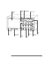
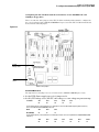
Display and
Graphical
Interface
Horizontal
controls
Acquisition and
general controls
Floppy Disk Drive
Trigger
Setup
Power
Marker and Quick
Measurements
Vertical
Inputs
Vertical
Controls
Auxiliary
Trigger Input
AutoProbe
Interface
iii
In This Book
This book provides the service documentation for the Agilent Technologies 54835A/45A/46A
oscilloscope. It is divided into eight chapters.
Chapter 1 provides general information and specifications.
Chapter 2 shows you how to prepare the oscilloscope for use.
Chapter 3 gives performance tests.
Chapter 4 covers calibration and adjustment procedures, how to do them, and how often they
need to be done.
Chapter 5 provides troubleshooting information.
Chapter 6 gives the procedures and techniques for replacing assemblies and other parts.
Chapter 7 includes a list of exchange assemblies and other replaceable parts, part ordering
information, and shipping information.
Chapter 8 briefly covers the internal operation of the oscilloscope.
At the back of the book you will find Safety information, Warranties, and Regulatory information.
iv
Contents
Contents 1
1
General Information 1-2
Instruments covered by this service guide 1-2
Accessories supplied 1-3
Options available 1-4
Accessories available 1-5
Specifications & characteristics 1-7
Agilent Technologies 54835A/45A/46A general characteristics 1-14
Recommended test equipment 1-16
2
Preparing for Use 2-2
Setting Up the Oscilloscope 2-3
To inspect the instrument 2-3
To connect power 2-4
To connect the mouse or other pointing device 2-5
To attach the optional trackball 2-5
To connect the keyboard 2-7
To connect to the LAN card 2-7
To connect oscilloscope probes 2-8
To connect a printer 2-9
To connect an external monitor 2-10
To connect the GPIB cable 2-10
To tilt the oscilloscope upward for easier viewing 2-11
To power on the oscilloscope 2-12
To verify basic oscilloscope operation 2-13
To clean the instrument 2-14
To clean the display monitor contrast filter 2-14
3
Testing Performance 3-2
Testing Interval 3-2
Equipment Required 3-2
Self-Test Verification 3-2
Test Record 3-3
Operating Hints 3-3
Specifications 3-3
Performance Test Procedures 3-3
To test the dc calibrator 3-4
To test input resistance 3-6
To test voltage measurement accuracy 3-7
To test offset accuracy 3-11
To test bandwidth 3-13
To test time measurement accuracy 3-16
To test trigger sensitivity 3-23
4
Calibrating and Adjusting 4-2
Equipment Required 4-2
Self Calibration Interval and Hardware Adjustments 4-2
Contents-1
Contents
Mainframe Cal Factor Memory Error 4-2
Operating Hints 4-3
Loading Default Oscilloscope Settings 4-3
Loading New Software 4-3
Calibration Procedures 4-3
To check the power supply 4-4
To check the 715 Hz auxiliary output (probe compensation squarewave) 4-6
To check the flat panel display (FPD) 4-7
To run the self calibration 4-10
5
Troubleshooting 5-2
Safety 5-2
Tools Required 5-2
ESD Precautions 5-2
Keystroke Conventions 5-2
Default Setup 5-3
To install the fan safety shield 5-3
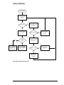
To troubleshoot the instrument 5-4
Primary Trouble Isolation 5-6
No Display Trouble Isolation 5-9
Power Supply Trouble Isolation 5-13
To check probe power outputs 5-16
To check the keyboard 5-17
To check the LEDs 5-19
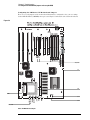
To check the motherboard, CPU, and RAM 5-21
To check the SVGA display board video signals 5-22
To check the backlight inverter voltages 5-23
POST Code Listing (AMI Motherboard only) 5-24
To configure the motherboard jumpers and set up the BIOS 5-29
To troubleshoot the acquisition system 5-49
To troubleshoot attenuator failures 5-56
Software Revisions 5-59
6
Replacing Assemblies 6-2
ESD Precautions 6-2
Tools Required 6-2
To return the instrument to Agilent Technologies for service 6-3
To remove and replace the cover 6-4
To disconnect and connect Mylar flex cables 6-5
To remove and replace the AutoProbe assembly 6-6
To remove and replace the probe power and control assembly 6-8
To remove and replace the backlight inverter board 6-9
To remove and replace the front panel assembly 6-9
To remove and replace the keyboard and flat-panel display assemblies 6-12
To remove and replace the acquisition board assembly 6-14
To remove and replace the LAN interface board 6-15
To remove and replace the GPIB interface board 6-16
To remove and replace the scope interface board and SVGA display board 6-17
To separate the scope interface board and SVGA display board 6-18
To remove and replace the Option 200 sound card 6-19
To remove and replace the hard disk drive 6-20
Contents–2
Contents
To remove and replace the floppy disk drive 6-21
To remove and replace the motherboard 6-21
To remove and replace the power supply 6-24
To remove and replace the fan 6-25
To remove and replace the CPU 6-26
To remove and replace RAM SIMMs or SDRAM DIMMs 6-27
To remove and replace an attenuator 6-28
To reset the attenuator contact counter 6-30
To remove and replace an acquisition hybrid 6-32
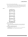
7
Replaceable Parts 7-2
Ordering Replaceable Parts 7-2
Power Cables and Plug Configurations 7-3
Exploded Views 7-4
Replaceable Parts List 7-15
8
Theory of Operation 8-3
Block-Level Theory 8-3
Attenuator Theory 8-7
Acquisition Theory 8-7
Contents–3
Contents-4
1
Instruments covered by this service guide 1-2
Accessories supplied 1-3
Options available 1-4
Accessories available 1-5
Specifications & characteristics 1-7
Agilent Technologies 54835A/45A/46A general characteristics 1-14
Recommended test equipment 1-16
General Information
General Information
This chapter of the Agilent Technologies Infiniium Oscilloscope Service Guide gives
you general information about the instrument. The following topics are covered in this
chapter.
•
•
•
•
•
Instrument identification
Options
Accessories
Specifications and characteristics
Test equipment requirements
Instruments covered by this service guide
On the rear panel of the instrument is a serial number label and a VIN # label. The serial number
is in the form of XX00000000 while the VIN # is in the form of VIN # 0XX. The serial number is
composed of two parts: the first two letters and the first four numbers are the serial prefix, while
the last four numbers are the suffix. The prefix is normally the same for all identical oscilloscopes
and changes only when a change has been made to the oscilloscope. However, the suffix is
sequentially assigned and is different for each oscilloscope. The contents of this manual applies
to oscilloscopes with serial number prefixes listed on the title page.
An oscilloscope manufactured after the printing of this manual may have a newer serial number
prefix. This newer serial prefix indicates that the oscilloscope may be different from those
described in this manual. The manual for this oscilloscope will be revised as needed. If you have
an oscilloscope with a newer serial prefix, please refer to the Agilent Technologies website and
download a newer manual edition in Adobe Acrobat (pdf) format. The Agilent Technologies
URL is: “www.agilent.com”. It will be necessary to search on a key word such as “Infiniium
Service Guide”, and follow the links.
For additional information on configuration differences see the following sections in this service
guide:
• “To configure the motherboard jumpers and setup the BIOS” in the Troubleshooting section
5 for information on determining:
•which computer configuration is contained in your oscilloscope
•setting up the BIOS correctly for that configuration
•setting the motherboard jumpers if the PC motherboard is changed.
• Replaceable Parts section 7.
This section contains exploded views for the different motherboard configurations, cabling
schemes, and outside hardware versions. The Replaceable Parts List also contains the
assembly part numbers for the different oscilloscope configurations.
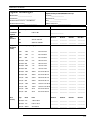
Table 1-1
Oscilloscopes Covered by this Service Guide
Model
Description
Agilent 54846A
Four-channel digitizing oscilloscope with 8 GSa/s sample rate in 2-channel mode, 4
GSa/s sample rate in 4-channel mode, 2.25 GHz bandwidth
Agilent 54845A
Four-channel digitizing oscilloscope with 8 GSa/s sample rate in 2-channel mode, 4
GSa/s sample rate in 4-channel mode, 1.5 GHz bandwidth
Agilent 54835A
Four-channel digitizing oscilloscope with 4 GSa/s sample rate in 2-channel mode,
2 GSa/s sample rate in 4-channel mode, 1 GHz bandwidth
The oscilloscope can be identified by the product number on the back panel.
1–2
Chapter 1: General Information
Accessories supplied
Accessories supplied
The following accessories are supplied.
• Agilent Mouse, Agilent P/N C3751-60201
• Agilent Mouse Pad, Agilent P/N 54810-85903
• 1 Keyboard
• (4) Agilent 1161A 10:1 10 MΩ passive probes
• Accessory Pouch (Agilent P/N 54810-68701)
• Power cord (see chapter 7, “Replaceable Parts,” for available power cords)
• User's Quick Start Guide
• Programmer’s Guide and Programmer’s Quick Reference
• Agilent Technologies Infiniium Oscilloscope Service Guide for Agilent Models
54835A/45A/46A (this manual)
1–3
Chapter 1: General Information
Options available
Options available
The following options are available for the Agilent Technologies Infiniium oscilloscope.
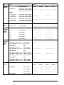
Table 1-2
Agilent Technologies Infiniium Oscilloscope Model 54835A/45A/46A Options
Option Number
Description
090
Delete standard probes
001
Add 2 standard probes—Agilent 1161A probes for the Agilent 54835A/45A/46A
002
Add 1 Agilent 1162A 1:1 passive probe
003
Add 1 Agilent 1163A 10:1 500 Ω, low-C passive probe
006
Add 1 Agilent 1152A 2.5 GHz, 0.6 pF active probe
007
Add 1 Agilent E2613A, 0.5 mm wedge kit assembly
008
Add 1 Agilent 1153A 200 MHz differential probe
009
Add 1 Agilent 1154A 500 MHz differential probe
010
Add 1 Agilent 1159A 1 GHz differential probe
100
Communication Mask Test Kit
200
VoiceControl Option
1BP
MIL-STD-45662A and ANSI/NCSL Z540 calibration with test data
1CM
Add 1 Rackmount kit (Agilent E2609A)
UL6
Add 1 Clip-on trackball pointing device (Agilent E2611A)
UL5
Add 1 touchpad pointing device (Agilent E2612A)
W32
3 years calibration service
W34
3 years return standards comp cal service
W50
5 years return repair service (additional 2 years)
W52
5 years return calibrations service
W54
5 years return standards comp cal service
Other options are available. See your Agilent Technologies Sales Representative. You can order
multiple options, or you can order most of these options separately, using the Agilent model
number or part number.
1–4
Chapter 1: General Information
Accessories available
Accessories available
The following accessories are available for use with the Agilent Technologies Infiniium
oscilloscope.
Table 1-3
Accessories for the Agilent Technologies Infiniium Oscilloscope Model 54835A/45A/46A
Agilent 1144A
800 MHz Active Probe
Requires Agilent 1142A power supply—Agilent 1144-61604 probe power extender also
required when using 2 or more Agilent 1144A active probes
Agilent 1144-61604
Power Probe Extender
Agilent 1145A
2-channel 750 MHz SMT active probe
Requires Agilent 1142A power supply
Agilent 1146A
Oscilloscope AC/DC Current Probe
Agilent 1152A
2.5 GHz, 10:1, 100 kΩ, 0.6 pF Active Probe
Agilent 1153A
200 MHz Differential Probe
Agilent 1155A
750 MHz 2-Channel, Low-Mass Active Probe
Agilent 1161A
Standard probes for the Agilent 54835A/45A/46A
Agilent 1162A
1:1 Passive Probe
Agilent 1163A
10:1 500-Ω, low-C Passive Probe
Agilent 1170A
500 MHz Low-Mass, miniature 10:1 10 MΩ Passive Probe
Agilent 1171A
500 MHz Low-Mass, miniature 10:1 10 MΩ Passive Probe
Agilent 1172A
500 MHz Low-Mass, miniature 20:1 10 MΩ Passive Probe
Agilent 1173A
500 MHz Low-Mass, miniature 20:1 10 MΩ Passive Probe
Agilent 1182A
Testmobile
Agilent 10020A
Resistive Divider Probe Kit
Agilent 10240B
BNC Blocking Capacitor
Agilent 10833A
GPIB cable, 1 m
Agilent 10833B
GPIB cable, 2 m
Agilent 10833C
GPIB cable, 4 m
Agilent 10833D
GPIB cable, 0.5 m
Agilent 11094B
75Ω Feedthrough Termination
Agilent 34810B
Benchlink Oscilloscope Software
Agilent 34398A +
Agilent 34399A
RS-232-C printer cable + adapter kit
Agilent 54006A
6 GHz, 10:1 (500 Ω) or 20:1 (1 kΩ), .25 pF
Agilent 01144-61604
1:2 probe power fan-out (for use with Agilent 1144A and Agilent 1145A)
Agilent C2950A
Parallel printer cable, 2 m
Agilent C2951A
Parallel printer cable, 3 m
Agilent E2610A
Keyboard
Agilent E2609A
Rackmount Kit
Agilent E2611A
Clip-on Track Ball Pointing Device
1–5
Chapter 1: General Information
Accessories available
Agilent E2612A
Touchpad Pointing Device
Agilent E2625A
Communication Mask Test Kit
Agilent 54810-68703
Service Kit (includes service software and fan safety shield)
Agilent 54801-00601
Fan Safety Shield (clips onto side of chassis with cover removed)
Agilent E2635A
Voice Control Retrofit Kit
Agilent E2636A
Microphone Replacement
1–6
Chapter 1: General Information
Specifications & characteristics
Specifications & characteristics
The following tables list the performance specifications and operating characteristics for the
Agilent Technologies 54835A/45A/46A oscilloscope. Asterisks (*) denotes warranted
specifications, all others are typical. Specifications are valid after a 30 minute warm-up period,
and within ± 5 °C from the self-calibration temperature.
Acquisition
Maximum Sample Rate
Real Time
Agilent Models
54835A — 2-channel mode: 4 GSa/s
54835A — 4-channel mode: 2 GSa/s
54845A — 2-channel mode: 8 GSa/s
54845A — 4-channel mode: 4 GSa/s
54846A — 2-channel mode: 8 GSa/s
54846A — 4-channel mode: 4 GSa/s
Maximum Effective Sample Rate
Equivalent Time
500 GSa/s
Memory Depth
2-channel mode: 65,536 points
4-channel mode: 32,768 points
Agilent 54835A, Agilent 54845A, and
Agilent 54846A
Memory Depth Modes
Auto
Optimized for best combination of
update rate and display quality.
Manual
Selectable
2-channel mode: from 16 to 65,536
points
4-channel mode: from 16 to 32,768
points
Real Time
Successive single shot acquisitions.
Equivalent Time
Random repetitive sampling (higher
time resolution at fast sweep speeds).
Sampling Modes
Filters
9-bit Bandwidth Limit filter: BW = (Sample Rate)/20
(Sin x)/x Interpolation: On/Off selectable FIR digital filter. Digital signal
processing adds points between acquired data points to enhance
measurement accuracy and waveform display quality.
BW= Sample Rate/4
Averaging
Selectable from 2 to 4096.
1–7
Chapter 1: General Information
Specifications & characteristics
Vertical
Number of Channels
4 (simultaneous acquisition)
Bandwidth
Analog Bandwidth (-3dB)*
50Ω: 1.0 GHz — Agilent 54835A
50Ω: 1.5 GHz — Agilent 54845A
50Ω: 2.25 GHz — Agilent 54846A
1 MΩ: 500 MHz (with Agilent 1161A probe)
System Bandwidth
Agilent 1161A 10:1 passive probe: 500 MHz
Agilent 1162A 1:1 passive probe: 25 MHz
Agilent 1163A 10:1, 500 Ω passive probe:
1.5 GHz
Agilent 1152A 2.5 GHz, 0.6 pF active probe:
1.3 GHz (Agilent 54845A)
Agilent 1152A 2.5 GHz, 0.6 pF active probe:
1.0 GHz (Agilent 54835A)
Agilent 1153A 200 MHz differential probe:
200 MHz
Real Time bandwidth*
50Ω:
Agilent 54835A — 1 GHz (2-channel mode)
Agilent 54835A — 500 MHz (4-channel mode)
Agilent 54845A — 1.5 GHz (2-channel mode)
Agilent 54845A — 1.0 GHz (4-channel mode)
Agilent 54846A — 2.25 GHz (2-channel mode)
Agilent 54846A — 1.0 GHz (4-channel mode)
1 MΩ: 500 MHz
Rise Time1
50Ω: 350 ps (Agilent 54835A)
50Ω: 233 ps (Agilent 54845A)
50Ω: 156 ps (Agilent 54846A)
1 MΩ: 700 ps
Sensitivity2
1 MΩ Coupling: 2 mV/div to 2 V/div
50 Ω Coupling: 2 mV/div to 1 V/div
Input Impedance*
1 MΩ ± 1% (≅12 pf), or 50 Ω ± 1.5%
VSWR (50 Ω)
54835A/45A
dc to 500 MHz: 1.30
500 MHz to 1 GHz: 1.50
1 GHz to 1.5 GHz: 1.75
Input Coupling
dc, ac (7 Hz, available in 1 MΩ only)
Maximum Input Voltage
1 MΩ: ± 100 V (dc + ac) [ac<10 kHz], CAT I
50 Ω: 5 Vrms, CAT I
Channel-to-channel Isolation
(with channels at equal
sensitivity)
54835A/54845A
dc to 100 MHz: 40 dB
100 MHz to 1 GHz: 30 dB
1 GHz to 1.5 GHz: 25 dB
54846A
dc to 100 MHz: 40 dB
100 MHz to 1 GHz: 30 dB
1 GHz to 2.25 GHz: 24 dB
Offset Range
Vertical Sensitivity
Available Offset
1 MΩ:
2 mV to 104 mV/div
> 104 mV to 2 V/div
50Ω: all
±4V
± 40 V
± 12 div
54846A
dc to 500 MHz: 1.30
500 MHz to 1 GHz: 1.50
1 GHz to 1.5 GHz: 1.75
1.5 GHz to 2.25 GHz: 2.50
Full-resolution channel
scales
10, 20, 50, 100, 200, 500, 1000 mV/div (plus 2000 mV/div in 1 MΩ)
Dynamic Range
± 8 div from center screen
dc Gain Accuracy
2
Resolution
1–8
*2
± 1.00% of full scale at full-resolution channel scale.
Real Time
8 bits (0.4% of full scale), 12 bits with
sufficient averaging (0.024% of full scale)
Equivalent Time
8 bits (0.4% of full scale), 12 bits with
sufficient averaging (0.024% of full scale)
Chapter 1: General Information
Specifications & characteristics
Offset Accuracy*2
± (1.00% of channel offset + 1% of full scale) at full-resolution channel scale.
dc Voltage Measurement
Accuracy*2
Dual Cursor
±[(dc gain accuracy)+(resolution)]
Single Cursor
±[(dc gain accuracy)
+(offset accuracy)+(resolution/2)]
AutoProbe Interface
AutoProbe is an intelligent communication and power link between compatible
probes and Infiniium scopes. AutoProbe completely configures the scope for the
attached probe. For instance, it identifies the probe type and sets up the proper input
impedance, attenuation ratio, probe power and offset range, as needed.
Horizontal
Main Time Base Range
100 ps/div to 20 s/div
Horizontal Position Range
pre-trigger
0 to -1 s or one full screen width,
whichever is larger.
post-trigger
0 to 1 s or one full screen width,
whichever is larger.
Delayed Sweep Range
1 ps/div to current main time base setting.
Delayed Sweep Delay Range
Within main time base acquisition record.
Resolution
2 ps
Timebase Accuracy
70 ppm (.007%)
∆t Accuracy*
Real Time mode4
±[(.007%)(∆t)+(0.2)(sample period)]
Equivalent Time mode
±[(.007%)(∆t)+(full scale/
(2 × memory depth)) + 30 ps]
(Example: for ≥ 16 avgs, 9 ns signal,
1 ns/div, 1 channel, then accuracy =
±[(.007%)(9 ns)+(10 ns/(2 × 65,536)) + 30
ps] = 31 ps)
1–9
Chapter 1: General Information
Specifications & characteristics
Trigger
Sensitivity*2
Internal
dc to 100 MHz: 0.5 div
100 MHz to 500 MHz: 1.0 div
500 MHz to 1 GHz: 1.5 div
Auxiliary
dc to 500 MHz: 300 mVpp
Maximum Input Voltage*
Auxiliary
±15 V, CAT I
Minimum Pulse Width
(internal, external)
500 ps at > 1.0 div
Level Range
Internal
±8 div from center screen
Auxiliary
±5 V
Sweep Modes
Auto, triggered, single
Trigger Coupling
dc, ac (7 Hz), low frequency reject (50 kHz), high frequency reject (50 kHz).
Trigger Holdoff Range
60 ns - 320 ms
Trigger Modes
Edge, Glitch, Pattern, State, Delay by Time, Delay by Events, Violation (
Setup/Hold Time, Pulse Width, Transition), Video, Line.
Glitch
Select positive or negative polarity, width. Captures glitches as narrow as 500 ps.
Pattern
Select inputs as High, Low or X (don’t care) to create pattern. Trigger when
pattern is entered, exited, present > t, present < t, or present over a range of
time. Captures patterns as narrow as 500 ps.
State
Select one channel as clock, specify other inputs as High, Low or X.
Logic Type: AND or NAND
Delay by Time
Time: 30 ns to 160 ms. The trigger is qualified by an edge. After the delay, a
rising/falling edge on any one selected input will generate the trigger.
Delay by Events
Events: 1 to 16,000,000 rising or falling edges. The trigger is qualified by an edge.
After the delay, a rising/falling edge on any one selected input will generate the
trigger.
Violation Trigger
Setup/Hold
Modes: Setup, Hold or Setup and Hold.
Select Clock, Thresholds, setup and/or
hold time.
Pulse Width
Triggers on pulse width >t, or <t.
Captures pulses as narrow as 500 ps.
Transition
Select Rise Time or Fall Time,
present > t or present < t, thresholds.
Accuracy (time) for glitch, pulse
width, and time-qualified pattern
1.5 ns - 20 ns: ±(20% setting + 500 ps)
20 ns - 160 ms: ±(3% setting + 2 ns)
Video Triggering
525 lines/60 Hz (NTSC), 625 lines/50 Hz (PAL), 875 lines/60 Hz. Trigger on Field 1
or Field 2, any line. User defined triggering: User can specify sync pulse level,
width and polarity, edge number.
1–10
Chapter 1: General Information
Specifications & characteristics
Display
Display
8.4-inch diagonal color active matrix LCD module incorporating amorphous
silicon TFTs.
Active Display Area
171 mm x 128 mm (21,888 sq. mm)
Waveform Viewing Area
104 mm x 159 mm (16,536 sq. mm) in Full screen mode
(graphical user interface off)
Display Resolution
640 pixels horizontally x 480 pixels vertically
Waveform Colors
Select from 100 hues, 0-100% saturation and 0-100% luminosity.
Dual Intensity Infinite Persistence
Previous sweeps are stored in half bright display and most recent sweep in full
bright. This allows easy differentiation of current and historic information.
Waveform Overlap
When two waveforms overlap, a third color distinguishes the overlap area.
Full screen mode
On/Off selectable.
Connect-the-dots
On/Off selectable.
Persistence
Minimum, Variable (100 ms to 40 s), Infinite. Up to 6 levels of grey scale.
Graticule
On/Off (Grid or Frame).
Grid Intensity
0 to 100%
Display Update Rate
(for instruments equipped with
AMD-K6-2 400 MHz processor)
Measurement Conditions
Real Time sampling mode, minimum
persistence, triggered sweep, no
interpolation, markers off, math off,
connect the dots off, 1 channel
acquisition, 50 ns/div, statistics off.
512 point record (2 GSa/s)
Waveforms/sec: > 2,100
Vpp Measurements/sec: > 130
Measurements
Automatic Parametrics
33 automatic measurements: Vpp , Vmin , Vmax ,Vavg , Vamptd , Vbase , Vtop, Vrms ,
Preshoot, Overshoot, Vupper , Vmiddle , Vlower , Rise Time, Fall Time, Period,
Frequency, Positive Width, Negative Width, Duty Cycle, Delta Time, Tmax , Tmin ,
FFT Frequency, FFT Magnitude, FFT Delta Frequency, FFT Delta Magnitude, Eye
Height, Eye Width, Jitter, Crossing %, Q-factor, Duty Cycle Distortion.
Over GPIB only: VTime, TVolts.
Threshold Definition
Selectable 10%, 50%, 90% or 20%, 50%, 80% or Custom (% or absolute voltage).
Top-Base Definition
Standard or Custom (in absolute voltage).
Statistics
On/Off selectable. Current measurement, mean, and standard deviation
Measurement Toolbar
16 Drag and Drop automatic measurement icons.
QuickMeas
Activates 4 preselected automatic measurements.
Markers Modes
Manual Markers, Track Waveform Data, Track Measurements.
Waveform Math
4 function waveforms f1-f4. Select from Add, Subtract, Multiply, Divide, Invert,
Magnify, Vs, Min, Max, Integral, Differentiate, FFT Magnitude.
1–11
Chapter 1: General Information
Specifications & characteristics
FFT
Frequency Range5
Agilent 54835A — 2-channel mode:
Agilent 54835A — 4-channel mode:
Agilent 54845A — 2-channel mode:
Agilent 54845A — 4-channel mode:
Agilent 54846A — 2-channel mode:
Agilent 54846A — 4-channel mode:
Freq. Accuracy
(1/2 frequency resolution)+(7x10⁻⁵)(signal frequency)
Amplitude Display
Power in dBm
Signal-to-noise ratio
70 dB at 32K memory depth. Noise floor varies with memory depth and with
averaging.
Window Modes
Hanning, Flattop, Rectangular.
dc to
dc to
dc to
dc to
dc to
dc to
2 GHz (Sample rate/2)
1 GHz (Sample rate/2)
4 GHz (Sample rate/2)
2 GHz (Sample rate/2)
4 GHz (Sample rate/2)
2 GHz (Sample rate/2)
Computer System/ Storage
CPU
AMD-K5™PR133 Microprocessor
(instrument serial numbers US37349999 and below) or
AMD-K6™ 200 MHz Microprocessor or
AMD-K6/300™ or AMD-K6-2/300™ 300 MHz Microprocessor
Disk Drive
1.4 GByte, 2.1 GByte, or higher
internal hard drive depending upon
the vintage. Storage capacity is
limited only by disk space. 3.5", 1.44
Mbyte MS-DOS™-compatible high
density floppy disk drive or LS-120
MS-DOS 120 MByte floppy disk
drive.
Store and recall setups, waveforms, and
store screen images to both the hard drive
and the floppy drive.
File types
Waveforms
Internal Y values; X and Y values in ASCII
or Microsoft Excel formats.
Images
BMP, EPS, GIF, PCX, PS (Postscript), TIF.
Mouse
Standard mouse supplied—supports any Microsoft® mouse compatible pointing
device, serial or PS/2.
Operating System
Microsoft Windows 95 or Microsoft Windows 98
Waveform Memories
4 nonvolatile waveform reference memories.
I/O
LAN
Enables data/setup file transfers and use of network printers; supports popular
network operating systems including Novell NetWare, Microsoft, Banyan VINES,
SCO UNIX and IBM; 10 Mbps operation that complies with IEEE 802.3 Ethernet and
ISO/IEC 8802-3 Ethernet standards; TCP/IP protocol; RJ-45 connector.
GPIB
Fully programmable, complies with IEEE 488.2.
RS-232 (serial)
2 ports: COM1, COM2. Printer and pointing device support.
Centronics
Printer port.
USB
Two pinheads link with Universal Serial Bus connectors (USB1 and USB2)
peripheral devices via either a dual-port USB cable or a single-port USB cable on
some configurations with serial prefixes US39480000 and above.
Printers and Plotters
Supports all printers and plotters compatible with Microsoft Windows95®. Includes
but is not limited to Hewlett-Packard Deskjet and Laserjet printers. GPIB devices
not supported.
PS/2 port
For PS/2 mouse.
Keyboard port
For optional keyboard.
1–12
Chapter 1: General Information
Specifications & characteristics
Video Output
15-pin VGA, full color.
Notes
1
Rise Time figures are calculated from: tr=.35/Bandwidth.
2
Magnification is used below the 10 mV/div range and between the major attenuation settings. Full scale
is defined as the major attenuator setting over an intermediate setting.
(Major settings for 50Ω: 10, 20, 50, 100, 200, 500, 1000 mV
Major settings for 1 MΩ: all as for 50Ω plus 2 V)
3
N/A
4
For bandwidth limited signals, tr >=1.4 x sample interval.
5
FFT amplitude readings are affected by input amplifier roll-off (-3 dB, with amplitude decreasing as
frequency increases above 500 MHz in 1 MΩ, 2.25 GHz for Agilent 54846A, 1.5 GHz in 50Ω for Agilent 54845A,
1 GHz in 50Ω for Agilent 54835A).
CAT I and CAT II Definitions
Installation category (overvoltage category) I: Signal level, special equipment or parts of
equipment, telecommunication, electronic, etc., with smaller transient overvoltages than
installation category (overvoltage category) II.
Installation category (overvoltage category) II: Local level, appliances, portable equipment etc.,
with smaller transient overvoltages than installation category (overvoltage category) III.
1–13
Chapter 1: General Information
Agilent Technologies 54835A/45A/46A general characteristics
Agilent Technologies 54835A/45A/46A general characteristics
The Infiniium oscilloscopes meet the Agilent Technologies Environmental Specification (section
750) for class B-1 products with exceptions as described for temperature.
General Characteristics
Environmental
Temperature
Operating: 10°C to +40°C
Nonoperating: –40°C to 70°C
Indoor use only
Humidity
Operating: Up to 95% relative humidity
(noncondensing) at +40°C
Nonoperating: Up to 90% relative
humidity at +65°C
Altitude
Operating: Up to 4 600 meters
Nonoperating: Up to 15 300 meters
Vibration
Operating: Random vibration 5-500 Hz,
10 minutes per axis, 0.3g (rms)
Nonoperating: Random vibration 5-500
Hz, 10 minutes per axis, 2.41g (rms)
Resonant search 5-500 Hz, swept sine,
1 octave/minute sweep rate, (0.75g),
5-minute resonant dwell at 4
resonances per axis.
Physical
Power
Safety
1–14
Size (excluding handle)
Height: 216 mm
Width: 437 mm
Depth: 440 mm
Weight
Net: approximately 12 kg
Shipping: approximately 15 kg
Line voltage selection
None, PFC (Power Factor Correction)
Line voltage range
100-240VAC, ± 10% CAT II
Line frequency
47 to 440 Hz
Maximum power consumption
390 W
Meets IEC1010-1 +A1, CSA certified to C22.2 No. 1010.1, Self certified to UL 3111.
Chapter 1: General Information
Agilent Technologies 54835A/45A/46A general characteristics
1–15
Chapter 1: General Information
Recommended test equipment
Recommended test equipment
The following table is a list of the test equipment required to test performance, calibrate and
adjust, and troubleshoot this instrument. The table indicates the critical specification of the test
equipment and for which procedure the equipment is necessary. Equipment other than the
recommended model may be used if it satisfies the critical specification listed in the table.
Recommended Test Equipment
Equipment Required
Critical Specifications
Recommended Model
Use *
Signal Generator
1 - 2.25 GHz, sine wave, amplitude 30 - 200
mVrms, time base accuracy 0.25 ppm
Agilent 8664A
P
RF Amplifier
22 dB gain at 10 MHz, 1.3 GHz bandwidth
Agilent 8447D/F
P
Power Meter/Power
Sensor
1 - 500 MHz, -70 dBm to +44 dBm, ±3% accuracy
Agilent EPM441A/Agilent 8482A
P
DMM
6 1/2 digit (0.1 mV) resolution, dcV accuracy
8 ppm/year, 4-wire resistance acc. ±0.25%
Agilent 34401A
P, A, T
Power Supply
7 mV - 30 V dc, 0.1 mV accuracy and resolution
Agilent 6114A
P
Power Splitter
50 Ω type N, outputs differ by <0.15 dB
Agilent 11667A
P
Probe
No substitute
Agilent 1161A
P
Probe Tip Adapter
1160 series to BNC
Agilent 5063-2143
P
Oscilloscope
General-purpose
Agilent 54622A
P, T
Blocking Capacitor
0.18 µF
Agilent 10240B
P
Cable
Type N (m)(m) - 3 foot
Agilent 11500A or B
P
Cable (2)
BNC - 3 foot
Agilent 10503A
P, A, T
Cable (3)
BNC - 9 inch
Agilent 10502A
P, A, T
Adapter
N (m) to BNC (m)
Agilent 1250-0082
P
Adapter
N (m) to BNC (f)
Agilent 1250-0780
P
Adapter
N (f) to BNC (m)
Agilent 1250-0077
A
Adapter (2)
BNC tee (m)(f)(f)
Agilent 1250-0781
P, T
Adapter
BNC (f)(f)
Agilent 1250-0080
T
Adapter (2)
BNC (f) to dual banana (m)
Agilent 1251-2277
P
Termination
BNC connectors 50 Ω
Agilent 10100C
P
Shorting cap
BNC
Agilent 1250-0774
P
Resistor (2)
5 Ω, 5 W
Agilent 0812-0047
T
Video monitor
Accepts VGA-standard video signals
Keyboard
PC-compatible, AT 5-pin connector
Agilent E2610A
T
Mouse
PS/2 compatible
Agilent C3751-60201
P, T
POST Card
Power-on self test card compatible with PCcompatible systems
Fan Safety Shield
Clips onto side of chassis with cover removed
Agilent 54801-00601
A, T
Service software
No substitution
Agilent 54810-68700
T
T
T
Note: the Fan Safety Shield and Service software are part of the Service Kit, Agilent P/N 54810-68703.
* P = Performance Tests, A = Adjustments, T = Troubleshooting
1–16
2
Setting Up the Oscilloscope 2-3
To inspect the instrument 2-3
To connect power 2-4
To connect the mouse or other pointing device 2-5
To attach the optional trackball 2-5
To connect the keyboard 2-7
To connect to the LAN card 2-7
To connect oscilloscope probes 2-8
To connect a printer 2-9
To connect an external monitor 2-10
To connect the GPIB cable 2-10
To tilt the oscilloscope upward for easier viewing 2-11
To power on the oscilloscope 2-12
To verify basic oscilloscope operation 2-13
To clean the instrument 2-14
To clean the display monitor contrast filter 2-14
Preparing for Use
Preparing for Use
This chapter shows you how to prepare the Agilent Technologies 54835A/45A/46A
oscilloscopes for use. The following areas are covered in this section.
•
•
•
•
Inspection
Setup
Connecting a signal
Cleaning
Following instrument setup is a brief section covering oscilloscope operation. If you are
unfamiliar with this oscilloscope's operation, refer to the User’s Quick Start Guide. The
topics covered include:
•
•
•
•
•
Using the front panel
Using the graphical interface
Starting and stopping acquisition
Adjusting oscilloscope configuration
Making measurements
The Infiniium Oscilloscope is designed to make it easy for you to use a high-performance
digitizing oscilloscope.
• The familiar front-panel oscilloscope interface with knobs and buttons is optimized
for the most common kinds of troubleshooting tasks and basic measurements.
• The graphical interface with menus, windows, dialogs, and toolbars provides easy
logical access to dozens of configuration and analysis tools, making it easy for you to
set up and make the most complex measurements.
2–2
Chapter 2: Preparing for Use
To inspect the instrument
Setting Up the Oscilloscope
This section will help you get the instrument ready to use. Included are procedures for:
•
•
•
•
•
•
Inspection
Connecting power
Connecting probes and accessories
Connecting peripherals
Verifying basic operation
Cleaning
To inspect the instrument
❏ Inspect the shipping container for damage.
Keep a damaged shipping container or cushioning material until the contents of the shipment
have been checked for completeness and the instrument has been checked mechanically and
electrically.
❏ Check the accessories.
Accessories supplied are listed in chapter 1 of this service guide.
• If the contents are incomplete or damaged notify your Agilent Technologies Sales Office.
❏ Inspect the instrument.
• If there is mechanical damage or defect, or if the instrument does not operate properly or pass
performance tests, notify your Agilent Technologies Sales Office.
• If the shipping container is damaged, or the cushioning materials show signs of stress, notify
the carrier as well as your Agilent Technologies Sales Office. Keep the shipping materials for
the carrier's inspection. The Agilent Technologies office will arrange for repair or replacement
at Agilent Technologies' option without waiting for claim settlement.
2–3
Chapter 2: Preparing for Use
To connect power
To connect power
The instrument Power Factor Correction (PFC) circuitry in the oscilloscope’s power supply
operates over a line voltage in the range of 100 to 240 Vac ±10% (the power supply is autoranging
to the input voltage and frequency). Line frequency must be in the range 47 to 440 Hz. Power
consumption is 390W maximum.
1 Position the instrument where it will have sufficient clearance for airflow around the
top, back, and sides.
Minimum 38.1 mm
Minimum 0 mm
Minimum 15.9 mm (maintained by feet; however,
do not place on soft surfaces that will impede
airflow)
Airflow requirements
Agilent 54835A/45A/46A – 250
Minimum
15.9 mm
both
sides
2 Connect the power cord to the rear of the oscilloscope, then to a suitable ac voltage
source.
The line cord provided is matched by Agilent Technologies to the country of origin of order.
Ensure that you have the correct line cord. See “Power Cables and Plug Configurations” in
chapter 7.
WAR N IN G
SHOCK HAZARD!
BEFORE YOU CONNECT THIS INSTRUMENT TO MAINS POWER OR LIVE MEASURING
CIRCUITS, you must provide a protective earth ground. Failure to provide a protective earth
ground could result in a shock hazard if there is a failure in this instrument or equipment
connected to it.
The mains plug must be inserted in a socket outlet provided with a protective earth contact.
Do not use an extension cord (power cable) without a protective conductor (grounding).
Grounding one conductor of a two-conductor outlet does not provide an instrument ground.
A Three-wire Power Cable is Provided
This instrument is provided with a three-wire power cable. When connected to an appropriate ac power
outlet, this cable grounds the instrument cabinet.
2–4
Chapter 2: Preparing for Use
To connect the mouse or other pointing device
To connect the mouse or other pointing device
• Plug the mouse into the matching connector on the back panel of the oscilloscope.
The mouse is included with the oscilloscope, but using it is optional. While you can operate many
oscilloscope functions with only the front-panel keys and knobs, you will need the mouse to
access advanced oscilloscope functions through the graphical interface, or to find out more about
the oscilloscope through the built-in information system.
The optional touchpad pointing device connects in exactly the same way as the mouse.
The supplied mousepad provides the correct surface for smooth mouse operation. To modify the
mouse configuration, see the User’s Quick Start Guide.
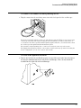
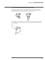
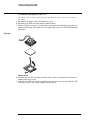
To attach the optional trackball
1 Push in the latch on the trackball baseplate to extend the metal tabs. Insert the lower
tab into the frontmost slot on the side of the oscilloscope. You can only install the
trackball on the right side of the oscilloscope.
2–5
Chapter 2: Preparing for Use
To attach the optional trackball
2 While holding the latch in, slide the metal tabs up and to the rear of the oscilloscope
until they fully engage the slot.
3 Release the latch. The trackball baseplate should now be secure against the side of the
oscilloscope.
4 Snap the trackball assembly onto the pins of the baseplate. The trackball and buttons
should face up and toward the front of the oscilloscope.
5 Connect the 9-pin “D” connector on the trackball cable to the COM1 port on the back
panel. Tighten the retaining screws.
For information on changing the trackball settings, see the User’s Quick Start Guide.
2–6
Chapter 2: Preparing for Use
To connect the keyboard
To connect the keyboard
• Plug the keyboard cable into the matching connector on the back panel of the
oscilloscope.
The keyboard simplifies access to some oscilloscope functions, such as entering file names when
you store waveforms and setups to the disk. If you need to free desk space, place the keyboard
on top of the instrument. Do not stack other objects on the keyboard; this will cause self-test
failures on power-on.
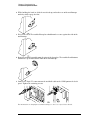
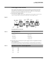
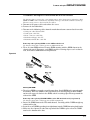
To connect to the LAN card
• Connect your LAN cable to one of the connectors on the LAN card. Make sure the
connection is secure. Two connections are possible on the LAN card: the RJ-45
connection and a BNC connection. Units equipped with 10/100Base-T LAN cards have
an RJ-45 connector only.
RJ-45 Connection
BNC Connection
Each Infiniium Oscilloscope now ships with a LAN card installed. If you want a LAN connection,
but have an older Infiniium Oscilloscope model that does not have a LAN card installed, contact
your Agilent Technologies Sales and Service Office. An Agilent Technologies LAN Card
Installation Kit with instructions is available from Agilent Technologies, and describes how to
add a LAN card to your Infiniium Oscilloscope. After you have connected to the LAN card, you
must set up the network as described in the User’s Quick Start Guide.
2–7
Chapter 2: Preparing for Use
To connect oscilloscope probes
To connect oscilloscope probes
1 Attach the probe BNC connector to the desired oscilloscope channel or trigger input.
Push it straight on until it latches into place.
2 Connect the probe to the circuit of interest using grabbers or other probing aids.
3 To disconnect the probe, push the small latch on top of the probe connector to the left,
then pull the connector body away from the front panel of the oscilloscope without
twisting it.
CA UT IO N
AVOID DAMAGE TO THE PROBE CONNECTOR!
Do not attempt to twist the snap-on probes on or off the oscilloscope’s BNC connector. Twisting
the probe connector body will damage it.
CA UT IO N
DO NOT EXCEED THE MAXIMUM INPUT VOLTAGE!
Do not exceed the maximum input voltage rating of the oscilloscope inputs! The maximum input
voltage for 50-Ω inputs is 5 Vrms, CAT I. The maximum input voltage for 1 MΩ inputs is ±100V
(dc+ac) [ac < 10 kHz], CAT I. (Probes may have different ratings. See the probe documentation.)
2–8
Chapter 2: Preparing for Use
To connect a printer
To connect a printer
If you have a parallel (Centronics) printer, you will need a parallel printer cable, such as an
Agilent C2950A (2 m) or Agilent C2951A (3 m) cable. Go to step 1.
If you have a serial printer, you will need a 9-pin to 25-pin serial printer cable, such as an
Agilent 34398A cable, plus the Agilent 34399A adapter kit. Some printers may require other cable
configurations, but the oscilloscope has a 9-pin serial connector. Go to step 4.
1 Attach the 25-pin small “D” connector to the printer output connector on the rear of
the oscilloscope. Tighten the thumbscrews to secure the cable.
2 Attach the larger 36-pin “D” connector to the printer. Latch the wire bails into the tabs
on each side of the connector.
3 Set the printer configuration to use the “Centronics” or “Parallel” interface, if
necessary. Refer to the User’s Quick Start Guide for software installation instructions.
See the documentation for your printer if you have questions about configuring the printer to
use the parallel interface.
4 Connect the 9-pin “D” connector of the serial printer cable to the serial output port on
the rear panel of the oscilloscope. Tighten the thumbscrews to secure the cable.
2–9
Chapter 2: Preparing for Use
To connect an external monitor
5 Attach the 25-pin “D” connector to the serial input port of the printer. Tighten the
thumbscrews to secure the cable.
6 Set the printer configuration to use the serial interface. Refer to the User’s Quick Start
Guide for software installation instructions.
See the documentation for your printer if you have questions about configuring the printer to
use the serial interface.
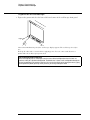
To connect an external monitor
You can connect a VGA-compatible monitor to the Infiniium oscilloscope to provide a larger
viewing area.
• Connect the monitor cable to the display board video connector at the rear panel of the
oscilloscope. Tighten the retaining screws.
To connect the GPIB cable
• Attach the GPIB connector to the GPIB interface card connector at the rear of the
oscilloscope. Tighten the thumbscrews on the connector.
2–10
Chapter 2: Preparing for Use
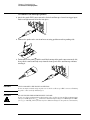
To tilt the oscilloscope upward for easier viewing
To tilt the oscilloscope upward for easier viewing
• If your oscilloscope has front feet with individual wire bails, lift up the front of the
oscilloscope, grasp one of the wire bails under the front corner, and pull it down and
forward until it latches into place. Repeat for the other wire bail.
• If your oscilloscope has front feet with a wire bail between the two feet, lift up the front
of the oscilloscope, grasp the bail near the center, and pull it down and forward until it
latches into place.
2–11
Chapter 2: Preparing for Use
To power on the oscilloscope
To power on the oscilloscope
• Depress the power switch at the lower left-hand corner of the oscilloscope front panel.
After a short initialization period, the oscilloscope display appears. The oscilloscope is ready to
use.
Hook up all cables and accessories before applying power. You can connect and disconnect
probes while the oscilloscope is powered-on.
You Can Configure the Backlight Saver
The oscilloscope display has a backlight saver that turns off the backlight when there has been no
interface activity for a pre-determined period. The default time is 8 hours and is configurable through the
Display Setup dialog in the graphical interface. You can turn the display on by moving the mouse, typing
on the optional keyboard, pressing a front-panel key, or turning a front-panel knob.
2–12
Chapter 2: Preparing for Use
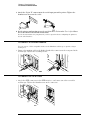
To verify basic oscilloscope operation
To verify basic oscilloscope operation
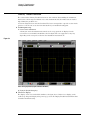
1 Connect an oscilloscope probe to channel 1.
2 Attach the probe to the calibration output on the front panel of the oscilloscope.
Use a probe grabber tip so you do not need to hold the probe. The calibration output is marked
with a square wave symbol.
Calibration
Output
3 Press the Default Setup key on the front panel.
The display will pause momentarily while the oscilloscope is configured to its default settings.
4 Press the Autoscale key on the front panel.
The display will pause momentarily while the oscilloscope adjusts the sweep speed and vertical
scale. You should then see a squarewave with peak-to-peak amplitude approximately 5 divisions
and a period of almost 3 divisions. If you do not see the waveform, ensure your power source is
adequate, the oscilloscope is properly powered-on, and the probe is connected securely to the
front-panel channel input BNC and to the probe calibration output.
5 Move the mouse pointer to the graphical interface enable button and click once.
The graphical interface enable button is in the upper-right corner of the display.
6 Move the mouse around the mouse pad and verify that the pointer follows on the
screen.
If the pointer does not move, ensure that the mouse is properly connected, that you have clicked
the correct button to enable the graphical interface, and that the mouse is on a medium-friction
surface such as the mouse pad supplied with the oscilloscope.
With the mouse pointer on
the right-hand button, click
the mouse to enable the
graphical interface
Graphical Interface Enable Button
2–13
Chapter 2: Preparing for Use
To clean the instrument
To clean the instrument
• Clean the oscilloscope with a soft cloth dampened with a mild soap and water solution.
CA UT IO N
BE CAREFUL TO AVOID DAMAGING COMPONENTS!
Do not use too much liquid when cleaning the oscilloscope. Water can enter the front panel
keyboard, damaging sensitive electronic components.
To clean the display monitor contrast filter
• Clean the display monitor contrast filter using glass cleaner and lens tissue or a soft cloth.
2–14
3
Testing Interval 3-2
Equipment Required 3-2
Self-Test Verification 3-2
Test Record 3-3
Operating Hints 3-3
Specifications 3-3
Performance Test Procedures 3-3
To test the dc calibrator 3-4
Procedure 3-4
To test input resistance 3-6
Procedure 3-6
To test voltage measurement accuracy 3-7
Procedure 3-7
To test offset accuracy 3-11
Procedure 3-11
To test bandwidth 3-13
Equivalent Time Test 3-13
Real Time Test 3-15
1 MΩ, 500 MHz Test 3-15
To test time measurement accuracy 3-16
Equivalent Time Mode Procedure 3-16
Real-Time Mode Procedure 3-21
To test trigger sensitivity 3-23
Internal Trigger Test 3-23
Procedure—Auxiliary Trigger Test 3-25
Testing Performance
Testing Performance
The procedures in this section test measurement performance using Performance
Specifications given in chapter 1 as performance standards. Specifications applicable to
individual tests are noted at the test for reference.
Testing Interval
The performance test procedures may be performed for incoming inspection of the
instrument and should be performed periodically thereafter to ensure and maintain peak
performance. The recommended test interval is yearly or every 2,000 hours of operation.
Test Interval Dependencies
The test interval depends on frequency and severity of use and the environmental conditions under which
the instrument is used. In recording test results, you may find that the test interval could be shortened or
lengthened; however, such a decision should be based on substantial quantitative data.
See Also
Chapter 4, “Calibrating and Adjusting,” for information about the calibration cycle.
Equipment Required
A complete list of equipment required for the performance tests is in the Recommended
Test Equipment table in chapter 1. Equipment required for individual tests is listed in
the test. Any equipment satisfying the critical specifications listed may be substituted
for the recommended model. The procedures are based on the model or part number
recommended.
Self-Test Verification
To verify system operation with high confidence, without the test equipment and time
required for performance tests, perform the self-tests. These internal tests verify many
functions of the oscilloscope.
To run the self-tests, enable the graphical interface, then select Self Test from the
Utilities menu. The Self Test drop down list box allows you to select Scope Self Tests,
Key and Knob Test, or LED Test. A message is displayed with the instruction to remove
all inputs to the instrument. During execution of the self-tests, the oscilloscope displays
diagnostic messages indicating the status of each test.
If one of the self-tests fails, FAILED is displayed rather than PASSED, and a 16-bit
diagnostic code is displayed. This code is used by factory service personnel when
troubleshooting the main assembly. Failure of a self-test indicates an assembly failure.
The assembly must be replaced before you attempt performance verification. For more
troubleshooting information, refer to chapter 5, “Troubleshooting.”
3–2
Chapter 3: Testing Performance
Test Record
You can record the results of the performance tests in the Performance Test Record
provided at the end of this chapter. The Performance Test Record lists the performance
tests and provides an area to mark test results. You can use the results recorded at
incoming inspection for later comparisons during periodic maintenance,
troubleshooting, and after repairs or adjustments.
Operating Hints
Some knowledge of operating the oscilloscope is helpful; however, these procedures are
written so that little experience is necessary. The following two hints will speed progress
of the testing.
Clear Display
When using many averages, it often takes awhile for a waveform display to stabilize after
a change. When a control on the oscilloscope is changed, averaging automatically
restarts. When just the input signal is changed, the instrument must average new data
with the old so it takes longer for the waveform to stabilize.
Press the Clear Display key while changing input signals. The instrument will restart
averaging and give a quick indication of the result of the signal change.
Averaging
Averaging is used to assure a stable signal for measurements. It is not necessary to wait
for complete stability of the signal (averaging complete), as long as the measurement is
well within the limits of the test.
Specifications
The specifications that apply to a particular test are given with the test procedure. The
specification as given with the test may be abbreviated for clarity. In case of any
questions, refer to the complete specifications and characteristics in chapter 1, “General
Information.”
Performance Test Procedures
Performance test procedures start with the next paragraph. Procedures may be done
individually and in any order.
Let the Instrument Warm Up Before Testing
Allow the instrument to warm up for at least 30 minutes prior to beginning performance tests. Failure to
allow warm-up may cause the instrument to fail tests.
3–3
Chapter 3: Testing Performance
To test the dc calibrator
To test the dc calibrator
The Aux Out BNC on the front panel is used for self-calibration and probe calibration. Though
calibrator accuracy is not specified in the performance specifications, it must be within limits in
order to provide accurate self-calibration.
Test Limits: -2.5 v to +2.5 v, Accuracy ±0.2% of delta voltage output
Equipment Required
Equipment
Critical Specifications
Recommended Model/Part
Digital Multimeter
0.1 mV resolution, better than 0.1 % accuracy
Agilent 34401A
Cable
BNC
Agilent 10503A
Adapter
BNC (f) to banana (m)
Agilent 1251-2277
Procedure
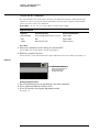
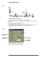
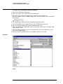
1 Connect the multimeter to the front panel Aux Out BNC.
Use the BNC cable and the BNC to banana plug adapter.
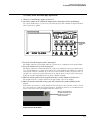
2 Enable the graphical interface.
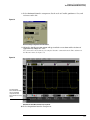
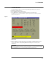
Use the mouse to click on the button in the upper right-hand corner of the display. See figure 3-1.
Figure 3-1
Click the mouse with the
pointer on the right-hand
button to enable the
graphical interface
Enabling the graphical interface
3 Press Default Setup to set the oscilloscope to default conditions.
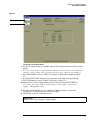
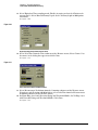
4 Select Calibration from the Utilities menu.
5 Select DC from the Aux Output drop-down list box.
See figure 3-2.
3–4
Chapter 3: Testing Performance
To test the dc calibrator
Figure 3-2
Set Aux Output to DC
Set the output voltage
Selecting DC in the Calibration Dialog
6 Set the dc output voltage to +2.500 V using the Level spin box or the numeric keypad
dialog.
You can access the numeric keypad dialog by clicking on the value in the Level box. Enter the
values by clicking on digits, signs, and exponents in the keypad. Click Close when finished.
7 The DVM should read near +2.500 V. Record the reading to four significant digits.
V1 = __________.
8 Set the level to -2.500 V using the Level spin box or the numeric keypad dialog.
9 The DVM should read near –2.500 V. Record the reading. V2 = __________.
10 Subtract the second reading from the first reading, then divide the result by 5.
For example, if the first reading is +2.498 V and the second reading is -2.497 V, then
V1 – V2
2.489 – ( – 2.497 )
-------------------- = ----------------------------------------- = 0.999
5
5
11 The final result should be between 0.998 and 1.002. Record the result in the
Performance Test Record at the end of the chapter.
12 Click Close to exit the calibration menu.
If the test fails
Repair is necessary. See chapter 5, “Troubleshooting.”
3–5
Chapter 3: Testing Performance
To test input resistance
To test input resistance
This test checks the input resistance of the vertical inputs. A four-wire measurement is used to
accurately measure the 50-Ω and 1-MΩ inputs.
Specification: 1 MΩ ±1% and 50 Ω ±1.5%
Equipment Required
Equipment
Critical Specifications
Recommended Model/Part
Digital Multimeter
Measure resistance (4-wire) at better than
0.25% accuracy
Agilent 34401A
Cables (2)
BNC
Agilent 10503A
Adapter
BNC Tee (m)(f)(f)
Agilent 1250-0781
Adapters (2)
BNC (f) to dual banana (m)
Agilent 1251-2277
Procedure
1 Set up the multimeter to make a four-wire resistance measurement.
2 Assemble the test cables.
a Use the two BNC-to-banana adapters to connect one end of each BNC cable to the fourwire resistance connections on the multimeter.
b Connect the free ends of the cables to the BNC tee.
See figure 3-3.
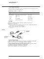
Figure 3-3
To ohmmeter
4-wire inputs
To oscilloscope
channel input
Input Resistance Equipment Setup
3 Connect the male end of the BNC tee to the channel 1 input of the oscilloscope.
4 Press Default Setup to set the oscilloscope to default conditions.
5 Press the Input key for Channel 1 to select 1 MΩ, then 50Ω, and verify resistance
readings of 1 MΩ ±10 kΩ and 50 Ω ±0.75 Ω respectively.
6 Record the readings in the Performance Test Record.
7 Repeat steps 3 through 6 on the remaining channels.
3–6
Chapter 3: Testing Performance
To test voltage measurement accuracy
To test voltage measurement accuracy
This test verifies the voltage measurement accuracy of the instrument. The measurement is made
using dual-cursor automatic measurement so that offset errors are not a factor.
A power supply provides a reference voltage to check voltage measurement accuracy. The actual
supply voltage is monitored for accuracy using a NIST-traceable voltmeter. A dc blocking
capacitor and a BNC short are used to filter any noise generated by the power supply (especially
at low voltages) so it does not appear at the oscilloscope input.
Specification
Only the dual-cursor specification is tested.
Single Cursor Measurement: ±(gain accuracy + offset accuracy + resolution/2)
Dual Cursor Measurement: ±(gain accuracy + resolution)
Gain Accuracy: ± 1.00% of full scale at full-resolution channel scale
Resolution: 8 bits, (0.4% of full scale without averaging); or
12 bits, (0.024% of full scale with 32 averages) at ful-resolution scale
Offset Accuracy: ±(1.00% of channel offset + 1% of full scale) at full-resolution scale
Equipment Required
Equipment
Critical Specifications
Recommended Model/Part
Power Supply
7 mV to 30 Vdc, 0.1 mV resolution
Agilent 6114A
Digital Multimeter
(DVM)
Better than 0.1% accuracy
Agilent 34401A
Cables (2)
BNC
Agilent 10503A
Adapters (2)
BNC (f) to banana (m)
Agilent 1251-2277
Adapters (2)
BNC tee (m)(f)(f)
Agilent 1250-0781
Blocking capacitor
0.18 µF
Agilent 10240B
Shorting cap
BNC
Agilent 1250-0774
Procedure
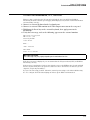
1 Connect the equipment.
See figure 3-4.
a Use a BNC-to-banana adapter to connect a BNC cable to the power supply.
b Connect a BNC tee to the other end of the cable and connect the tee to channel 1 of the
oscilloscope.
c Connect another BNC cable to the tee at the oscilloscope and connect a BNC tee to the
other end of the cable.
d Connect the blocking capacitor to the BNC tee and connect the BNC short to the blocking
capacitor.
e Connect a BNC-to-banana adapter to the same BNC tee and connect the adapter to the
DVM input.
3–7
Chapter 3: Testing Performance
To test voltage measurement accuracy
Figure 3-4
Voltage Measurement Accuracy Equipment Setup
2 Press Default Setup to set the oscilloscope to default conditions.
3 Set all channels to dc using the Coupling key and to 1 MΩ input impedance using the
Input key.
4 Using the mouse, enable the graphical interface.
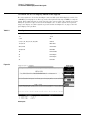
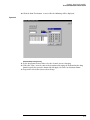
5 Select Acquisition from the Setup menu.
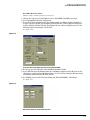
6 Select Equivalent Time sampling mode. Enable Averaging. Set the # of Averages to 32,
either using the spin box or the numeric keypad dialog. Click Close.
See figure 3-5.
Figure 3-5
Select Equivalent Time
sampling mode
Leave Memory Depth
on Automatic
Enable averaging
Set the number of
averages to 32
Acquisition Setup for Voltage Accuracy Measurement
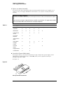
7 Use the following table for steps 8 through 15.
3–8
Chapter 3: Testing Performance
To test voltage measurement accuracy
Scale
Offset
Supply
Tolerance
Limits
2 V/div*
2.5 V
5V
±163.8 V
4.836 V to 5.164 V
1 V/div
2.5 V
5V
±82 mV
4.918 to 5.082 V
500 mV
1.75 V
3.5 V
±41 mV
3.459 to 3.541 V
200 mV
700 mV
1.4 V
±16.4 mV
1.384 to 1.416 V
100 mV
350 mV
700 mV
±8.2 mV
691.8 mV to 708.2 mV
50 mV
175 mV
350 mV
±4.1 mV
345.9 mV to 354.1 mV
20 mV
70 mV
140 mV
±1.64 mV
138.36 mV to 141.64 mV
10 mV
35 mV
70 mV
±0.819 mV
69.18 mV to 70.82 mV
* only in 1 MΩ input
Below 10 mV/div expansion is used and full scale is defined as 80 mV. The ranges
from 2 to 9 mV/div are handled in firmware, and will be within specifications when the
10 mV/div range is within specifications.
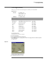
8 Select Vavg from the Voltage submenu of the Measure menu. Ensure that Channel 1 is
selected in the Source dialog and click Close.
See figure 3-6.
Figure 3-6
Select Channel 1 as the
source for the Vavg
measurement
Source Selection for Vavg Measurement
9 Select Channel 1 from the Setup menu.
10 Set the vertical scaling for Channel 1 to the volts/div value from the first row of the
table in step 7. Set the Offset value to the Position value from the first row of the same
table. Click Close.
See figure 3-7.
3–9
Chapter 3: Testing Performance
To test voltage measurement accuracy
Figure 3-7
Set the scale from the
table
Set the offset from the
table
Vertical Scaling and Offset for Voltage Accuracy Measurement
To Set Vertical Scale and Position
You can also use the knobs to set the vertical scale and position, but it is usually easier to use the dialog
box, particularly for the fine position setting.
11 With the supply disconnected from the channel input, note the Vavg mean reading.
____________ V
It may take a moment for this value to settle because of averaging.
12 Set the power supply voltage from the first line of the table. Use the voltmeter to adjust
the power supply for the most accurate output.
13 Connect the power supply to the channel input and note the Vavg reading. _________ V
Press Clear Display and wait a moment to read the value (so that averaging is complete).
14 Subtract the value in step 11 from the value in step 13. Record the difference in the
Performance Test Record.
15 On the same channel, repeat steps 10 through 14 for the rest of the rows in the table.
16 With the channel keys, set the active channel OFF and the next ON.
A channel is ON if its key is illuminated and OFF if it is not illuminated.
17 Move the BNC tee to the next channel and repeat steps 8 through 15 for that channel.
18 Repeat steps 8 through 17 for the rest of the channels.
19 Repeat steps 3 through 18 for the 50Ω input.
If the test fails
Voltage measurement errors can be caused by the need for self-calibration. Before troubleshooting the
instrument, perform self-calibration. See “To run the self-calibration” in chapter 4, “Calibrating and
Adjusting.” If self-calibration fails to correct the problem, the cause may be the attenuator or main
assembly.
3–10
Chapter 3: Testing Performance
To test offset accuracy
To test offset accuracy
This test checks the vertical offset accuracy.
Specification: ±(1.00% of channel offset + 1% of full scale) at full-resolution channel scale
Equipment Required
Equipment
Critical Specifications
Recommended Model/Part
Power Supply
0.5 V to 2 Vdc, ±1 mV accuracy
Agilent 6114A
Digital Multimeter
(DVM)
Better than 0.1% accuracy
Agilent 34401A
Cables (2)
BNC
Agilent 10503A
Adapters (2)
BNC (f) to banana (m)
Agilent 1251-2277
Adapters (2)
BNC tee (m)(f)(f)
Agilent 1250-0781
Blocking capacitor
0.18 µF
Agilent 10240B
Shorting cap
BNC
Agilent 1250-0774
Procedure
1 Connect the equipment.
The cabling is the same as that used for the voltage measurement accuracy test. See figure 3-4.
a Use a BNC-to-banana adapter to connect a BNC cable to the power supply.
b Connect a BNC tee to the other end of the cable and connect the tee to channel 1 of the
oscilloscope.
c Connect another BNC cable to the tee at the oscilloscope and connect a BNC tee to the
other end of the cable.
d Connect the blocking capacitor to the BNC tee and connect the BNC short to the blocking
capacitor.
e Connect a BNC-to-banana adapter to the same BNC tee and connect the adapter to the
DVM input.
2 Press Default Setup to set the oscilloscope to default conditions.
3 Select Acquisition from the Setup menu.
4 Select Equivalent Time under Sampling Mode. Enable Averaging, and set the # Points
for averaging to 32. Click Close.
Setup is the same as that for the voltage measurement accuracy test. See figure 3-5.
5 Use the following table for steps 6 through 12.
Volts/div
Position
Supply
Tolerance
Limits
minimum
maximum
200 mV
2.00000 V
2.00 V
±36 mV
1.964 V
2.036 V
100 mV
1.00000 V
1.00 V
±18 mV
0.982 V
1.018 V
50 mV
500.000 mV
500 mV
±9 mV
491 mV
509 mV
6 Select Channel 1 from the Setup menu.
7 Set the vertical Scale to the Volts/div value from the first row of the table. Set the Offset
to the Position value from the first row of the table. Click Close.
3–11
Chapter 3: Testing Performance
To test offset accuracy
8 Set the supply voltage to 2.00 V as in the first row of the table. Use the DVM to verify
the setting.
9 Re-adjust the vertical position, if necessary, so the trace is as close to the horizontal
center line of the grid as possible after it has settled (averaging complete).
10 Read the position voltage. It should be equal to the DVM reading, within the limits given
in the table. Record the reading in the Performance Test Record.
To find the current position setting, select Channel 1 from the Setup menu and read the Offset
field. Click Close when finished.
11
12
13
14
Repeat steps 6 through 10 for the other lines in the table.
With the channel keys, set the active channel OFF and the next ON.
Move the BNC from one channel to the next.
Repeat steps 6 through 13 for each channel, setting the parameters of the channel being
tested where appropriate.
If the test fails
Offset errors can be caused by the need for self-calibration. Perform self-calibration (see chapter 4,
“Calibrating and Adjusting”) before troubleshooting the instrument.
3–12
Chapter 3: Testing Performance
To test bandwidth
To test bandwidth
This test checks the bandwidth of the oscilloscope. The Agilent 54845A bandwidth at 1.5 GHz
and the Agilent 54846A bandwidth at 2.25 GHz oscilloscopes are checked using aliasing since
the trigger specification of these oscilloscopes is 1 GHz. The 1.5 GHz or the 2.25 GHz signal is
viewed with a time/division setting of approximately 50 µs/div where the on-screen display is an
untriggered sinewave that appears to be at a lower frequency, however the vertical response of
the amplifiers is correct. The Agilent 54835A bandwidth at 1.0 GHz and 500 MHz of all three
models is checked normally.
Specification
Equivalent Time:
50Ω: 2.25 GHz (Agilent 54846A), 1.5 GHz (Agilent 54845A), 1.0 GHz (Agilent 54835A)
1 MΩ: 500 MHz (with Agilent 1161A probe)
Real Time:
50Ω: for Agilent 54846A — 2.25 GHz (2-channel mode), 1.0 GHz (4-channel mode)
50Ω: for Agilent 54845A — 1.5 GHz (2-channel mode), 1.0 GHz (4-channel mode)
50Ω: for Agilent 54835A — 1.0 GHz (2-channel mode), 500 MHz (4-channel mode)
1 MΩ: 500 MHz (with Agilent 1161A probe)
Equipment Required
Equipment
Critical Specifications
Recommended Model/Part
Signal Generator
10—2250 MHz at ≈200 mVrms
Agilent 8664A
Power Meter/Sensor
1—1.5 GHz ±3% accuracy
Agilent EPM-441A/8482A
Power Splitter
outputs differ by <0.15 dB
Agilent 11667A
Cable
Type N (m) 24 inch
Agilent 11500B
Termination
50Ω, BNC Connectors
Agilent 10100C
Adapter
Type N (m) to BNC (m)
Agilent 1250-0082
Probe
No Substitute
Agilent 1161A
Probe Tip Adapter
1160 Series to BNC
Agilent 5063-2143
Equivalent Time Test
1 Connect the equipment.
a With the N cable, connect the signal generator to the power splitter input. Connect the
power sensor to one output of the power splitter.
b With an N-to-BNC adapter, connect the other splitter output to the channel 1 input.
2 Press Default Setup to set the oscilloscope to default conditions.
3 Select Acquisition from the Setup menu. Select Equivalent Time sampling mode. Click
Close. Select Display from the Setup Menu. Unselect Connect Dots mode. Click Close.
4 Set the vertical scale for Channel 1 to 100 mV/div using the knob. Select 50Ω input
impedance.
5 Set the sweep speed to 50 ns/div using the horizontal sweep speed knob.
6 Set the signal generator for 10 MHz at +5.0 dBm.
The signal on the oscilloscope screen should be about five cycles at six divisions amplitude.
Bandwidth Check Limits
Do not exceed 6 divisions when making the bandwidth check.
3–13
Chapter 3: Testing Performance
To test bandwidth
7 Select Vamptd from the Voltage submenu of the Measure menu.
8 Note the Vamptd (1) reading at the bottom of the screen. V10MHz =_______________mV.
9 Set the power meter Cal Factor % to the 10 MHz value from the calibration chart on
the power sensor. Then press dB[REF] on the power meter to set a 0 dB reference.
This establishes the baseline output power at 10 MHz as a reference for the bandwidth
measurement.
10 Change the signal generator output frequency to 1000 MHz for Agilent 54835A,
1500 MHz for Agilent 54845A, or 2250 MHz for Agilent 54846A. Set the power meter
chart Cal Factor % to the 2250 MHz value, to the 1500 MHz value, or to the 1000 MHz
value depending on the model number.
This step compensates the power meter reading for changes in the power sensor output at
1000 MHz, 1500 MHz, or 2250 MHz with respect to 10 MHz.
11 Adjust the signal generator output amplitude for a power reading as close as possible
to 0.0 dB[REL]. Write down the actual reading. Reading = ______ dB [REL].
The reading on the power meter will be used to correct the final bandwidth value.
12 Use one of the following steps depending on the Infiniium oscilloscope model being
tested and the bandwidth acquisition mode:
a (Use this step for model 54835A 1000 MHz Equivalent Time bandwidth check.)
Set the sweep speed to 500 ps/div using the Horizontal sweep speed knob.
b (Use this step for model 54845A 1500 MHz Equivalent Time bandwidth check.)
Set the sweep speed to 50 µs/div using the Horizontal sweep speed knob.
c (Use this step for model 54846A 2250 MHz Equivalent Time bandwidth check.)
Set the sweep speed to 50 µs/div using the Horizontal sweep speed knob.
d (Use this step for Real Time bandwidth checks: 1000 MHz on 54835A, 1500 MHz on
54845A, or 2250 MHz on 54836A)
Set the sweep speed to 500 ps/div using the Horizontal sweep speed knob.
e (Use this step for 1 MΩ, 500 MHz bandwidth check for all three models.)
Set the sweep speed to 1 ns/div using the Horizontal sweep speed knob.
13 Press the Clear Display key followed by the Run key to display a trace. (It there is no
trace on the screen slowly adjust the Trigger Level knob through zero until a trace is
displayed.) Note the Vamptd(1) reading.
V2250MHz = _______________ mV (54846A)
V1500MHz = _______________ mV (54845A)
V1000MHz = _______________ mV (54835A)
14 Calculate the response using the formula:
V 1500 MHz
response ( dB ) = 20log 10 ------------------------ = 20log 10 ________=_______dB
V 10 MHz
For example:
487 mV
20log 10 ------------------- = 20log 10 0.871 = – 1.19dB
559 mV
15 Correct the result from step 14 with any difference in the power meter from step 11.
Observe signs. For example:
Result from step 14 = -1.19 dB
Power meter reading = −0.5 dB(REL)
then true response = (−1.19)−(−0.5) = −0.69 dB
(__________) − (__________) = _________dB
16 The result from step 15 should be between +3.0 dB and −3.0 dB. Record the result in
the Test Record.
17 Switch the power splitter from the channel 1 to the channel 2 input.
18 Turn off the current channel and turn on the next channel using the channel keys.
3–14
Chapter 3: Testing Performance
To test bandwidth
19 Repeat steps 4 through 18 for the remaining channels, setting the parameters of the
channel being tested where appropriate.
Real Time Test
20 Select Acquisition from the Setup menu.
21 Select Real Time sampling mode, 8 GSa/s (Agilent 54845A and 54846A) or 4 GSa/s
22
23
24
25
(Agilent 54835A) configuration, then click Close.
Repeat steps 4 through 19, testing channels 1 and 3 to the 2.25 GHz limit (54846A), 1.5
GHz limit (Agilent 54845A), or the 1.0 GHz limit (Agilent 54835A).
Select Acquisition from the Setup menu.
Select the 4 GSa/s configuration (Agilent 54845A and 54846A) or 2 GSa/s configuration
(Agilent 54835A), then click Close.
Repeat steps 4 through 19, testing channels 1, 2, 3, and 4 to the 1 GHz limit (Agilent
54845A and 54846A) or the 500 MHz limit (Agilent 54835A).
1 MΩ, 500 MHz Test on 54835A, 54845A, and 54846A
Disconnect the power splitter from the channel input.
Select Acquisition from the Setup menu.
Select Equivalent time Sampling Mode and click Close.
Connect the Agilent 1161A 10:1 probe to channel 1. Verify that the probe compensation
is correct.
30 Change channel to 100 mV/div using the knob.
31 Connect the probe tip to the power splitter using the probe-tip-to-BNC adapter and 50Ω
termination.
32 Repeat steps 5 through 19, testing the 500 MHz limit on channels 1, 2, 3, and 4.
26
27
28
29
If the test fails
Failure of the bandwidth test can be caused by a faulty attenuator or main assembly. A self calibration
may correct a bandwidth failure.
3–15
Chapter 3: Testing Performance
To test time measurement accuracy
To test time measurement accuracy
This test uses a precise frequency source to check the accuracy of time measurement functions.
Specification Delta-t accuracy
Equivalent Time: (≥16 averages)
±[(0.007% × delta-t) + (full scale/(2 × memory depth))+ 30 ps]
Real Time: * ±[(0.007% × delta-t) + (0.2 × sample period)]
* The specification applies to bandwidth limited signals (tr ≥ 1.4 × sample period).
The sample period is defined as 1/(sample rate). The specification also applies to those
automatic measurements computing time intervals on identical slope edges
(like pos-pos, neg-neg).
Equipment Required
Equipment
Critical Specifications
Recommended Model/Part
Signal Generator
1-100 MHz,
timebase accuracy - 0.25 ppm
Agilent 8664A
RF Amplifier
40 MHz to 1 GHz, 20 dB gain
Agilent 8447D
Cable
Type-N 24 inch
Agilent 11500B
Cable
BNC
Agilent 10503A
Adapter
Type N (f) to BNC (m)
Agilent 1250-0077
The Agilent 8447D RF Amplifier is used as a saturation amplifier to create a very low-jitter
squarewave from the sinewave output of the signal generator. You adjust the signal generator
output level to change the risetime of the squarewave.
Equivalent Time Mode Procedure
This test checks time measurement in equivalent time mode with averaging.
1 Set the Agilent 8664A signal generator for a 40-MHz sine wave (25.0 ns period) at
250 mVrms.
2 Connect the output of the signal generator to the INPUT of the Agilent 8447D RF
3
4
5
6
7
amplifier.
Connect the OUTPUT of the RF amplifier to the channel 1 input of the oscilloscope.
Press Default Setup to set the oscilloscope to default conditions.
Press Input to select 50 Ω. Press Coupling to select dc.
Press Autoscale.
Set the vertical scale to 500 mV per division.
3–16
Chapter 3: Testing Performance
To test time measurement accuracy
8 Select horizontal from the setup mean. Set the scale to 5 ns/div, position at –5 ns, and
reference to the left.
Figure 3-8
Horizontal Setup for Equivalent Time Procedure
9 Adjust the signal generator output voltage to obtain a waveform with a risetime of
approximately 700 ps to 1.4 ns.
You can measure the risetime by selecting the Risetime command from the Time submenu of
the Measure menu. See figure 3-9.
Figure 3-9
Use the risetime
measurement to verify
correct waveform
shape for the time
measurement accuracy
check
Waveform for Time Measurement Accuracy Check
10 Select Acquisition from the Setup menu.
3–17
Chapter 3: Testing Performance
To test time measurement accuracy
11 Select Equivalent Time sampling mode. Enable Averaging and set the # Points to be
averaged to 16. Select Manual Memory Depth. Set the memory depth to 2004 points.
Click Close.
See figure 3-10.
Figure 3-10
Acquisition Setup for Equivalent Time Procedure
12 Select Delta Time from the Time submenu of the Measure menu. Select Channel 1 as
the source in the dialog that appears and click Close.
See figure 3-11.
Figure 3-11
Source Selection for Delta Time Measurement
13 Select Measurement Definitions from the Customize submenu of the Measure menu.
(If you have code Revision A.03.00 or higher, select Delta Time from the Measurements
Definitions submenu of the Measure menu.)
14 Set From Edge # to 1 with Direction Rising and Threshold Middle. Set To Edge # to 2
with Direction Rising and Threshold Middle. Click Close.
See figure 3-12.
3–18
Chapter 3: Testing Performance
To test time measurement accuracy
Figure 3-12
Measurement Settings for Time Interval Measurement
For valid statistical data
In equivalent time mode, measurement specifications are valid with sixteen or more acquisitions averaged.
Statistics accumulated before the required number of averaged acquisitions may show the instrument to
fail the specification. This is particularly true for minimum and maximum in this case since they are set by
measurements taken with the fewest averages.
If the procedure above is followed exactly, the required number of acquisitions are averaged before
statistics are turned on. Therefore, if you clear and restart measurements, averaging and statistics are
restarted simultaneously and the result is erroneous data collected from the early averages.
If in doubt about the statistical data, after #Avg is complete select Clear Measurements or Clear All from
the Measure menu tool bar, then repeat the custom measurement again. This restarts the statistics without
restarting averaging and the result is valid statistical data.
15 Verify the period is 25 ns ± 44 ps, minimum 24.956 ns and maximum 25.044 ns. Record
the minimum and maximum readings in the Performance Test Record.
16 Change the signal generator frequency to 100 MHz (10 ns period).
17 Select horizontal from the setup menu. Set the position to –11 ns.
18 Clear measurement statistics.
Do this by clicking Clear Meas (Clear All) on the measurement toolbar, then selecting Delta time
from the Time submenu of the measure menu.
19 The delta time reading should be 10 ns ± 43 ps, minimum 9.957 ns and
20
21
22
23
24
25
maximum 10.043 ns. Record the minimum and maximum readings in the
Performance Test Record.
Change the signal generator frequency to 20 MHz (50 ns period).
Select horizontal from the setup menu. Set the scale to 100 ns/div, position to –11 ns.
Clear measurement statistics as in step 18 and restart the measurement.
The delta time reading should be 50 ns ± 283 ps; minimum 49.72 ns and maximum
50.28 ns. Record the minimum and maximum readings in the Performance Test Record.
Change the signal generator frequency to 1 MHz (1 µs period).
Select horizontal from the setup menu. Set the scale to 1 µs/div, position to –11 ns.
3–19
Chapter 3: Testing Performance
To test time measurement accuracy
26 Clear measurement statistics as in step 18 and restart the measurement.
27 The delta time reading should be 1 µs ± 2.595 ns, minimum 997.4 ns and maximum
1.0026 µs. Record the minimum and maximum readings in the Performance Test
Record.
28 Select Measurement Definitions from the Customize submenu of the Measure menu.
(If you have code Revision A.03.00 or higher, select Delta Time from the Measurements
Definitions submenu of the Measure menu.)
29 Set the To Edge # to 6 with Direction Rising and Threshold Middle. Click Close.
See figure 3-13.
Figure 3-13
New Measurement Settings for Delta Time Measurement
30 Clear measurement statistics as in step 18 and restart the measurement.
31 The delta time readings should be 5 µs ± 2.875 ns, minimum 4.9971 µs and maximum
5.0029 µs. Record the minimum and maximum readings in the Performance Test
Record.
3–20
Chapter 3: Testing Performance
To test time measurement accuracy
Real-Time Mode Procedure
This procedure continues from the previous one.
1 Change the signal generator frequency to 25.31646 MHz (39.49999 ns period).
2 Select Acquisition from the Setup menu.
3 Select Real Time sampling mode. Set Configuration to 8 GSa/s (Agilent 54845A) or
4 GSa/s (Agilent 54835A). Set Sampling Rate to Manual, 8 GSa/s (Agilent 54845A) or
4 GSa/s (Agilent 54835A). Enable Averaging with the number of points set to 16. Set
Memory Depth to Automatic. Click Close.
See figure 3-14.
Figure 3-14
Acquisition Setup for Real Mode Procedure (showing Agilent 54845A)
4 Set sweep speed to 50 ns/div with horizontal position at 0.0 s.
5 Select Measurement Definitions from the Customize submenu of the Measure menu.
(If you have code Revision A.03.00 or higher, select Delta Time from the Measurements
Definitions submenu of the Measure menu.)
6 Set To Edge # to 11 with Direction Rising and Threshold Middle. Click Close.
See figure 3-15.
Figure 3-15
Measurement Definitions for Real Mode Procedure
3–21
Chapter 3: Testing Performance
To test time measurement accuracy
7 Clear measurements.
8 Select Period from the Time submenu of the Measure menu.
9 Period should be the following.
For Agilent 54835A: 39.50 ns ± 53 ps, minimum 39.447 ns, maximum 39.553 ns. Record
the minimum and maximum readings in the Performance Test Record.
For Agilent 54845A: 39.50 ns ± 28 ps, minimum 39.47 ns, maximum 39.53 ns. Record the
minimum and maximum readings in the Performance Test Record.
10 Select Delta Time from the Time submenu of the Measure menu.
11 Delta time should read the following:
For Agilent 54835A: 395 ns ± 78 ps, minimum 394.922 ns, maximum 395.078 ns. Record
the minimum and maximum readings in the Performance Test Record.
For Agilent 54845A: 395 ns ± 53 ps, minimum 394.947 ns, maximum 395.053 ns. Record
the minimum and maximum readings in the Performance Test Record.
12 Press the Stop key on the front panel.
13 Press the Sweep key (in the Trigger section of the front panel) to highlight the LED
14
15
16
17
18
19
labeled “Single.”
Press the Clear Display key.
Set the timebase to 1 µs/div.
Press the Run key once.
Select Measurement Definitions from the Customize submenu of the Measure menu.
(If you have code Revision A.03.00 or higher, select Delta Time from the Measurements
Definitions submenu of the Measure menu.)
Set the To Edge # to 101 with Direction Rising and Threshold Middle. Click Close.
Delta time mean should read the following:
For Agilent 54835A: 3.949999 µs ± 326 ps, minimum 3.949673 µs, maximum 3.950326
µs. Record the reading in the Performance Test Record.
For Agilent 54845A: 3.94999 µs ± 301 ps, minimum 3.949688 µs, maximum 3.950291 µs.
Record the reading in the Performance Test Record.
20 Select Measurement Definitions from the Customize submenu of the Measure menu.
(If you have code Revision A.03.00 or higher, select Delta Time from the Measurements
Definitions submenu of the Measure menu.)
21 Set the To Edge # to 201. Click Close.
22 The Delta Time mean should read the following:
For Agilent 54835A: 7.89999 µs ± 603 ps, minimum 7.899395 µs and maximum 7.90060
µs. Record the reading in the Performance Test Record.
For Agilent 54845A: 7.89999 µs ± 578 ps, minimum 7.89942 µs and maximum 7.90058
µs. Record the reading in the Performance Test Record.
23 Click Close.
If the test fails
Before troubleshooting the oscilloscope, be sure to verify your test setup and the waveform shape, then
repeat the procedure. Try the measurement on different channels. If you still encounter problems, there
may be a problem with the acquisition board. You may need to adjust the pulse overshoot response. See
chapter 4 for adjustment information on the pulse response. See chapter 5 for troubleshooting information.
3–22
Chapter 3: Testing Performance
To test trigger sensitivity
To test trigger sensitivity
This test checks channel and external triggers for sensitivity at rated bandwidth.
Specification
Internal:
dc to 500 MHz: 0.5 div
100 MHz to 500 MHz: 1.0 div
500 MHz to 1 GHz: 1.5 div
Auxiliary:
dc to 500 MHz: 300 mVpp
Equipment Required
Equipment
Critical Specifications
Recommended Model/Part
Signal Generator
100 and 500 MHz, 1.0 GHz, 30-80 mVrms output
Agilent 8664A
Power Splitter
outputs differ by <0.15 dB
Agilent 11667A
Termination
BNC feedthrough, 50 Ω
Agilent 10100C
Cable
Type N (m) 24 inch
Agilent 11500B
Cable
50 Ω BNC 36 inch
Agilent 10503A
Adapter
Type N (f) to BNC (m)
Agilent 1250-0077
Adapter
Type N (m) to BNC (m)
Agilent 1250-0082
Adapter
Type N (m) to BNC (f)
Agilent 1250-0780
Adapter
BNC tee (m)(f)(f)
Agilent 1250-0781
Internal Trigger Test
Perform this test on all vertical channels.
1 Press Default Setup.
2 Select Acquisition from the Setup menu.
3 Select Equivalent time sampling mode. Enable Averaging and set the number of points
to 4. Click Close.
See figure 3-16.
Figure 3-16
Acquisition Setup for Trigger Sensitivity Test
4 Set horizontal time/div to 5 ns/div.
3–23
Chapter 3: Testing Performance
To test trigger sensitivity
5 Turn on Channel 1 and turn off all other channels.
You can do this by using the channel keys above each input BNC or by using the check boxes at
the top of the waveform display area.
6 Set vertical scale for channel 1 to 200 mV/div. Select dc coupling and 50Ω input
impedance.
7 With an N cable and N-to-BNC adapter, connect the signal generator to the channel 1
input.
8 Set the signal frequency to 100 MHz and output level for 0.5 divisions of vertical
deflection.
You can use the markers to set a 0.5 division reference. Select Markers from the Measure menu
and select Manual Placement in the dialog that appears. Both Markers should be set to the same
channel. Set the Y value for Marker A to +50.0 mV and the Y value for Marker B to –50.0 mV,
then click Close. (If the markers do not appear on the screen, press the Marker A and Marker B
keys on the front panel.) See figure 3-17.
Figure 3-17
Setting the Markers for a 0.5 Division Reference
9 Press the Sweep key (Trigger section of the front panel controls) to select Trig’d.
The scope’s Armed and Trig’d LEDs (in the Horizontal section of the front panel) should flash.
However, the waveform display may not be stable.
10 Adjust the trigger level control for a stable display.
11 The test passes if triggering is stable. Record the result in the Performance Test Record.
12 Set the signal frequency to 500 MHz and the output level for 1 division of vertical
deflection.
Again, you can use the markers to check the deflection, with one set to +100 mV and the other
to –100 mV.
13
14
15
16
Adjust the horizontal sweep speed to 1 ns/div.
Adjust the trigger level for a stable display.
The test passes if triggering is stable. Record the result in the Performance Test Record.
Set the signal frequency to 1.0 GHz and the output level for 1.5 division of vertical
deflection.
Again, you can use the markers to check the deflection, with one set to +150 mV and the other
to –150 mV.
3–24
Chapter 3: Testing Performance
To test trigger sensitivity
17
18
19
20
21
Adjust the horizontal sweep speed to 1 ns/div.
Adjust the trigger level for a stable display.
The test passes if triggering is stable. Record the result in the Performance Test Record.
Connect the signal generator to the channel 2 input.
Repeat steps 4 through 20 for the remaining channels.
Procedure—Auxiliary Trigger Test
The auxiliary trigger input is on the front panel of the oscilloscope near the vertical inputs. The
dc input resistance of the aux trigger is 2.58kΩ, so to avoid reflections, the trigger source is backterminated with 50 Ω.
1 With an N-to-BNC adapter and BNC cable, connect the signal generator to the input of
2
3
4
5
6
7
the power splitter. Connect one output of the power splitter to the Aux Trig input
through a 50 Ω feedthrough termination. Connect the other output of the power splitter
to channel 1.
Set the signal generator for 500 MHz, approximately 0 dBm.
Set the channel 1 input to 50-Ω input impedance and press Autoscale.
Set the channel 1 scaling to 50 mV/div. Then set the signal generator for 6 divisions of
signal (300 mVpp).
Press the Source key (Trigger section of front panel) to highlight Aux.
Set the trigger level to 0.000 V.
Slowly adjust the Trigger Level knob slightly around the 0 V setting to obtain a stable
trigger. Otherwise, the test fails. Record the result in the Performance Test Record.
If a test fails
Failure of the internal trigger or external trigger sensitivity tests can be caused by a defective main
assembly or attenuator. Failure of the auxiliary trigger sensitivity is caused by a problem on the main
assembly or a bad input cable. If you need further troubleshooting information, go to chapter 5,
“Troubleshooting.”
3–25
3–26
Performance Test Record
Agilent Technologies
Agilent Technologies 54835A/45A/46A Oscilloscope
Model Number _____________________
Tested by___________________
Serial Number ___________________________
Work Order No.___________________
Recommended Test Interval - 1 Year/2000 hours
Date___________________
Recommended next testing___________________
Ambient temperature ___________________
Test
dc Calibrator
Amplitude
Input
Resistance
Voltage
Measurement
Accuracy
Offset
Accuracy
Limits
Results
(Vmax - Vmin)/5 =
Limits
1.000
0.998 to 1.002
___________________
Channel 1
Channel 2
Channel 3
Chan 4/Ext
50Ω
49.25 Ω to 50.75 Ω
___________
___________
___________
___________
1 MΩ
990 kΩ to 1.010 MΩ
___________
___________
___________
___________
Scale
Coupling
Supply
Limits
Channel 1
Channel 2
Channel 3
Channel 4
2 V/div
1 MΩ
5V
4.836 V to 5.164 V
___________
___________
___________
___________
1 V/div
1 MΩ
5V
4.918 V to 5.082 V
___________
___________
___________
___________
1 V/div
50Ω
5V
4.918 V to 5.082 V
___________
___________
___________
___________
500 mV/div 1 MΩ
3.5 V
3.459 V to 3.541 V
___________
___________
___________
___________
500 mV/div 50Ω
3.5 V
3.459 V to 3.541 V
___________
___________
___________
___________
200 mV/div 1 MΩ
1.4 V
1.384 V to 1.416 V
___________
___________
___________
___________
200 mV/div 50Ω
1.4 V
1.384 V to 1.416 V
___________
___________
___________
___________
100 mV/div 1 MΩ
700 mV
691.8 mV to 708.2 mV
___________
___________
___________
___________
100 mV/div 50Ω
700 mV
691.8 mV to 708.2 mV
___________
___________
___________
___________
50 mV/div
1 MΩ
350 mV
345.9 mV to 354.1 mV
___________
___________
___________
___________
50 mV/div
50Ω
350 mV
345.9 mV to 354.1 mV
___________
___________
___________
___________
20 mV/div
1 MΩ
140 mV
138.36 mV to 141.64 mV ___________
___________
___________
___________
20 mV/div
50Ω
140 mV
138.36 mV to 141.64 mV ___________
___________
___________
___________
10 mV/div
1 MΩ
70 mV
69.18 mV to 70.82 mV
___________
___________
___________
___________
10 mV/div
50Ω
70 mV
69.18 mV to 70.82 mV
___________
___________
___________
___________
Range
Offset
Limits
Channel 1
Channel 2
Channel 3
Channel 4
200 mV/div 2.0 V
1.964 to 2.036 V
___________
___________
___________
___________
100 mV/div 1.0 V
0.982 to 1.018 V
___________
___________
___________
___________
50 mV/div
491 to 509 mV
___________
___________
___________
___________
500 mV
3–27
Test
Bandwidth
(50Ω Input)
Limits
Results
Down from reference:
Equivalent Time
Channel 1
Agilent 54835A <3.0 dB at 1000 MHz ___________
Agilent 54845A <3.0 dB at 1500 MHz
Agilent 54846A <3.0 dB at 2250 MHz
Channel 2
Channel 3
Channel 4
___________
___________
___________
Realtime
Bandwidth
(1 MΩ
Input)
Time
measurement
accuracy—
equivalent
time mode
Time
measurement
accuracy—
real time
mode
2 channel (4 GSa/s)
2 channel (8 GSa/s)
2 channel (8 GSa/s)
Agilent 54835A <3.0 dB at 1000 MHz ___________
Agilent 54845A <3.0 dB at 1500 MHz
Agilent 54846A <3.0 dB at 2250 MHz
4 channel (2 GSa/s)
4 channel (4 GSa/s)
4 channel (4 GSa/s)
Agilent 54835A <3.0 dB at 500 MHz ___________
Agilent 54845A <3.0 dB at 1000 MHz
Agilent 54846A <3.0 dB at 1000 MHz
___________
___________
___________
Down from reference:
Channel 1
Channel 2
Channel 3
Channel 4
With 1161A Probe
<3.0 dB at 500 MHz
___________
___________
___________
___________
∆Time
Limits
Minimum
Maximum
25 ns
24.946 to 25.044 ns
__________________
__________________
10 ns
9.957 to 10.043 ns
__________________
__________________
50 ns
49.72 to 50.28 ns
__________________
__________________
1 µs
997.4 to 1.0026 µs
__________________
__________________
5 µs
4.9971 to 5.0029 µs
__________________
__________________
Minimum
Maximum
__________________
__________________
__________________
__________________
Agilent 54835A: 3.949999 µs ± 326 ps 3.949673 to 3.950326 µs __________________
Agilent 54845A: 3.949999 µs ± 301 ps 3.949688 to 3.950291 µs
Agilent 54846A: 3.949999 µs ± 301 ps 3.949688 to 3.950291 µs
__________________
Period
Limits
Agilent 54835A: 39.50 ns ± 53 ps
39.447 to 39.553 ns
Agilent 54845A/46A: 39.50 ns ± 28 ps 39.47 to 39.53 ns
∆Time (edge#11)
Limits
Agilent 54835A: 395 ns ± 78 ps
Agilent 54845A/46A: 395 ns ± 53 ps
394.922 to 395.078 ns
394.947 to 395.053 ns
∆Time (edge#101)
Limits
∆Time (edge#201)
___________
Limits
Agilent 54835A: 7.89999 µs ± 603 ps 7.899395 to 7.90060 µs __________________
Agilent 54845A: 7.89999 µs ± 578 ps 7.89942 to 7.90058 µs
Agilent 54846A: 7.89999 µs ± 578 ps 7.89942 to 7.90058 µs
Trigger
Sensitivity
Mode
Stable Trigger On:
Internal Trigger
Auxiliary Trigger
3–28
__________________
Pass/Fail
Channel 1
Channel 2
Channel 3
Channel 4
0.5 div at 100 MHz
___________
___________
___________
___________
1.0 div at 500 MHz
___________
___________
___________
___________
1.5 div at 1.0 GHz
___________
___________
___________
___________
300 mVpp at 500 MHz
___________
___________
___________
___________
4
Equipment Required 4-2
Self Calibration Interval and Hardware Adjustments 4-2
Mainframe Cal Factor Memory Error 4-2
Operating Hints 4-3
Loading Default Oscilloscope Settings 4-3
Loading New Software 4-3
Calibration Procedures 4-3
To check the power supply 4-4
To check the 715 Hz auxiliary output (probe compensation squarewave) 4-6
To check the flat panel display (FPD) 4-7
To run the self calibration 4-10
Calibrating and Adjusting
Calibrating and Adjusting
This chapter provides firmware (self calibration) and hardware adjustment procedures
for the Agilent Technologies 54835A/45A/46A oscilloscope.
•
•
•
•
Power Supply Check
Oscillator Check
Flat-Panel Display Check
self calibration
Equipment Required
Equipment required for adjustments is listed in the Recommended Test Equipment
table in chapter 1 of this manual. Any equipment that satisfies the critical specification
listed in the table may be substituted for the recommended model. Equipment for
individual procedures is listed at the procedure.
Self Calibration Interval and Hardware Adjustments
The firmware calibration is the self cal (self calibration). Self calibration should be done
every year, or every 2,000 hours of operation, whichever comes first. The hardware
adjustment consists of checking the power supply, 715 Hz calibration output (probe
compensation squarewave), and flat-panel display. These adjustments only need to be
done under circumstances set by certain needs, which are explained in other areas of
this guide.
The self calibration uses signals generated in the oscilloscope to calibrate channel
sensitivity, offsets, and trigger parameters. You should run the self calibration
•
•
•
•
•
yearly, or according to your periodic needs,
when you adjust or replace the acquisition assembly or acquisition hybrids,
when you replace the hard drive or any other assembly,
when the delta temperature is more than ±5 °C different than the last calibration, or
after performing incoming performance verification and before performing outgoing
performance verification.
The need for self calibration will also depend on your experience and on the environment
in which you use the oscilloscope.
Mainframe Cal Factor Memory Error
If power is applied to the oscilloscope and the message “Mainframe cal factor memory
error: Please perform calibration” is displayed, you must calibrate the oscilloscope. See
“To run the self calibration” in this chapter.
If the oscilloscope does not pass the self calibration, repair is necessary.
4–2
Chapter 4: Calibrating and Adjusting
Operating Hints
Some knowledge of operating the Agilent Technologies 54835A/45A/46A oscilloscope is
helpful. However, procedures are written so that little experience is necessary. The
following hints will speed progress of the procedures.
When using many averages, it often takes awhile for a waveform display to stabilize after
a change. When a front panel control on the oscilloscope is changed, averaging
automatically restarts. When the input signal or an adjustment is changed, the
oscilloscope averages new data with the old, so it takes longer for the waveform to
stabilize to the new value. Press the Clear Display key while changing input signals or
adjustments. Clearing the display restarts averaging, which gives a quicker indication
of the result of the change.
Loading Default Oscilloscope Settings
To reset the oscilloscope to default conditions, press the Default Setup key.
Loading New Software
This oscilloscope stores its operating system code on a hard disk drive. New code is
loaded into the oscilloscope by using the floppy disk drive. It is rarely necessary to reload
the code. You should load the code only if prompted by a troubleshooting procedure, or
if you want to load a later version of code.
To load new code, enable the graphical interface, then select Upgrade Software from
the Utilities menu. You can then follow the instructions on the screen, inserting diskettes
as necessary.
Calibration Procedures
The procedures start with the next paragraphs. Unless specified elsewhere, procedures
must be followed in the order given. Display checks are optional and independent of
other procedures.
Let the Oscilloscope Warm Up Before Adjusting
Warm up the oscilloscope for 30 minutes before starting adjustment procedures. Failure to allow warmup may result in inaccurate calibration.
WAR N IN G
SHOCK HAZARD!
Read the Safety information at the back of this guide before performing adjustment procedures.
Failure to observe safety precautions may result in electrical shock.
WAR N IN G
INJURY CAN RESULT!
Install the fan safety shield (included in the Service Kit) if you remove the oscilloscope cover.
Without this shield, the oscilloscope fan blades are exposed and can cause injury.
4–3
Chapter 4: Calibrating and Adjusting
To check the power supply
To check the power supply
There are no adjustments for the supply. Perform this procedure only if you suspect a power
supply problem.
Equipment Required
Equipment
Critical Specifications
Recommended Model/Part
Digital Voltmeter
Accuracy ±0.05%
Agilent 34401A
Procedure
1 Disconnect the oscilloscope power cord and remove the cover.
If necessary, refer to the procedures in chapter 6, “Replacing Assemblies.”
WAR N IN G
INJURY CAN RESULT!
Use care when working around the oscilloscope with the cover off and power applied. The fan
blades are exposed and could cause injury; also, there is approximately 900 V generated by the
backlight inverter for the flat-panel display.
2 Connect the oscilloscope power cord and set power switch to ON.
3 Refer to the following figure for testpoint locations.
Figure 4-1
Power Supply Test Points
4–4
Chapter 4: Calibrating and Adjusting
To check the power supply
4 Connect the common lead of the voltmeter to the GND test point.
5 Connect the positive lead of the voltmeter to the +5.1 V test point.
6 Verify that the +5.1 supply voltage is within limits as shown in the following table:
Table 4-1
Power Supply Voltage Limits
Supply Voltage Specification
Limits
+5.1 V ± 0.1 V
+5.0 V to +5.2 V
-5.2 V ± 0.1 V
-5.1 V to -5.3 V
+12.2 V ± 0.3 V
+11.9 V to +12.5 V
-12.2 V ± 0.3 V
-11.9 V to -12.5 V
+15 V bias
+14 V to +16 V
7 Repeat steps 4 through 6 for each of the other supply voltages.
If any supply voltage is not within specifications, see chapter 5, “Troubleshooting.”
4–5
Chapter 4: Calibrating and Adjusting
To check the 715 Hz auxiliary output (probe compensation squarewave)
To check the 715 Hz auxiliary output (probe compensation squarewave)
This test is optional. The 715 Hz auxiliary output is not specified in the oscilloscope performance
specifications. The values given are typical. Results are not recorded in the Performance Test
Record.
Equipment Required
You can check the 715 Hz auxiliary output using the scope itself.
Procedure
1
2
3
4
5
6
7
Press Default Setup.
Use a BNC cable to connect the front panel Aux Out to the Channel 1 input.
Set Coupling to DC and Input to 50Ω for Channel 1.
Press Autoscale.
Select Vamptd from the Voltage submenu of the Measure menu.
Select Frequency from the Time submenu of the Measure menu.
The signal should be a squarewave at approximately 715 Hz with amplitude of
approximately 300 mVpp.
4–6
Chapter 4: Calibrating and Adjusting
To check the flat panel display (FPD)
To check the flat panel display (FPD)
No equipment is required for this procedure. Specifications for flat-panel displays used in the
Infiniium oscilloscope are shown in the following table.
Flat-Panel Display Specifications
Defect Type
Polarizer
Dot Defect
(A dot is defined as 1, 2, or 3 stuck
subpixels touching horizontally.
Subpixels are horizontal red, green,
blue triads, so these may show up as
one of 8 colors or black.)
Limit
Scratch
Width ≤ 0.05 mm
Length ≤ 10 mm
Dent
φ ≤ 0.4mm
Bright dot
N≤5
Dark dot
N≤7
Total dot
N ≤ 12
Two adjacent dots
Bright dot
Dark dot
≤ 2 pairs
≤ 2 pairs
Three or more adjacent dots
Not allowed
Distance between defects
Bright dot
Dark dot
≥ 10 mm
≥ 10 mm
Line Defect
Not allowed
Non-uniformity
Check other specifications
Luminance
(The measurement is perpendicular
to the screen surface in both axes.)
Minimum
Typical
160 cd/m2
200 cd/m2
When to Use this Procedure
This procedure should not be performed as a part of routine maintenance. Perform the procedure only
when there appears to be a problem with the display.
1
2
3
4
Enable the graphical interface.
Select Self Test from the Utilities menu.
Click the Service Extensions box in the Self Test dialog.
Select Screen from the Test drop-down list box.
See figure 4-2.
4–7
Chapter 4: Calibrating and Adjusting
To check the flat panel display (FPD)
Figure 4-2
Click to start the
test
Select Screen to do
the flat-panel
display test
Starting the Screen Test
5 Click Start.
A new dialog appears with a series of radio buttons that allow selection of different background
colors. See figure 4-3.
4–8
Chapter 4: Calibrating and Adjusting
To check the flat panel display (FPD)
Figure 4-3
Click one of these
buttons to select the
background color to
check
Screen Test
6 Select a color by clicking the radio button for that color.
7 Carefully check the colored region for pixels colored differently than the current
selection.
These pixels are either inactive or stuck. If black (when a color or white is selected), they are
inactive; if another color than the current selection, but not black, then they are stuck. If the
display does not meet the specification given on the previous page, replace it. See chapter 6 for
removal and replacement procedures.
8 Repeat steps 6 and 7 for all colors.
4–9
Chapter 4: Calibrating and Adjusting
To run the self calibration
To run the self calibration
The self calibration uses signals generated in the oscilloscope to calibrate channel sensitivity,
offsets, and trigger parameters. You should run the self calibration
• yearly, or according to your periodic needs,
• when you adjust or replace the acquisition assembly or acquisition hybrids,
• when you replace the hard drive or any other assembly,
• when the delta temperature is more than ±5 °C different than the last calibration, or
• after performing incoming performance verification and before performing outgoing
performance verification.
Equipment Required
Equipment
Critical Specifications
Recommended Model/Part
Cable
BNC 50 Ω 9 inch
Agilent 10502A
Let the Oscilloscope Warm Up Before Running the Self Calibration
The self calibration should only be done after the oscilloscope has run for one half hour at ambient
temperature with the cover installed. Calibration of an oscilloscope that has not warmed up may result in
performance test failure.
self calibration
Calibration time
It will take approximately 45 minutes to run the self calibration on the oscilloscope, including the time
required to change cables from channel to channel.
1 Enable the graphical interface.
2 Select Calibration from the Utilities menu.
3 If the Cal Memory Protect box in the Calibration dialog is checked, click the check box
to clear the check mark.
See figure 4-4.
4–10
Chapter 4: Calibrating and Adjusting
To run the self calibration
Figure 4-4
Clear this check
box before starting
calibration
Click here to start
calibration
Calibration Dialog
Clear Cal Memory Protect to Run self calibration
You cannot run self calibration if this box is checked.
4 Click Start, then follow the instructions on the screen.
You will be asked first to disconnect all channels and the Aux Output, then to connect Aux Out
to each channel and the auxiliary trigger in turn. After you complete each cable change, click
OK in the dialog box to continue the calibration.
The oscilloscope displays a Passed/Failed message as each calibration routine is completed.
5 After calibration has been completed, click to check the Cal Memory Protect box to
protect the calibration memory. Then click Close.
If calibration fails
Go to chapter 5 “Troubleshooting.”
4–11
4–12
5
Safety 5-2
Tools Required 5-2
ESD Precautions 5-2
Keystroke Conventions 5-2
Default Setup 5-3
To install the fan safety shield 5-3
To troubleshoot the instrument 5-4
Primary Trouble Isolation 5-6
No Display Trouble Isolation 5-9
Power Supply Trouble Isolation 5-13
To check probe power outputs 5-16
To check the keyboard 5-17
Test Procedure 5-17
Troubleshooting Procedure 5-18
To check the LEDs 5-19
To check the motherboard, CPU, and RAM 5-21
To check the SVGA display board video signals 5-22
To check the backlight inverter voltages 5-23
POST Code Listing (AMI Motherboard only) 5-24
To configure the motherboard jumpers and set up the BIOS 5-29
Motherboard / floppy drive configurations BIOS setup 5-29
Configuring the AMI Series 727 Motherboard Jumpers 5-32
To configure the AMI Series 727 WINBIOS Parameters 5-34
Configuring the AMI Series 757 Motherboard for 200 MHz CPU 5-37
To configure the AMI Series 757 WINBIOS Parameters with 1.44 Mbyte floppy drive 5-39
Configuring the AMI Series 757 Motherboard for 300 MHz CPU 5-42
To configure the AMI Series 757 WINBIOS Parameters with 120 Mbyte floppy drive 5-44
Configuring the FIC VA-503A motherboard switches for the 400 MHz CPU and 120 Mbyte
floppy drive 5-47
To Configure the FIC Series VA-503A Motherboard BIOS Parameters 5-48
To troubleshoot the acquisition system 5-49
Determining the Acquisition Contact Closure Count 5-49
Isolating Acquisition Problems 5-49
To troubleshoot attenuator failures 5-56
Attenuator Click Test 5-56
Swapping Attenuators 5-57
Attenuator Connectivity Test 5-57
Software Revisions 5-59
Troubleshooting
Troubleshooting
This section provides troubleshooting information for the Agilent Technologies
54835A/45A/46A oscilloscope. The service strategy of this instrument is replacement of
defective assemblies.
Safety
Read the Safety Summary at the front of this manual before servicing the instrument.
Before performing any procedure, review it for cautions and warnings.
WAR N IN G
SHOCK HAZARD!
Maintenance should be performed by trained service personnel aware of the hazards involved
(for example, fire and electric shock). Lack of training and awareness of the hazards could result
in electrical shock. When maintenance can be performed without power applied, the power cord
should be removed from the instrument.
WAR N IN G
INJURY CAN RESULT!
Use caution when working around the cooling fan with the cover removed from the instrument.
The cooling fan blades are exposed on one side and can be hazardous. Install the optional fan
safety shield (Agilent Technologies P/N 54801-00601) to protect your fingers from the fan blades.
Tools Required
You will need basic electronic troubleshooting tools, including a digital multimeter and
a 100-MHz oscilloscope. Performance verification tests have more stringent
requirements. See chapter 1 for the list of recommended test equipment.
If you need to remove and replace assemblies, you will need some of the hand tools listed
in chapter 6, “Replacing Assemblies.”
ESD Precautions
When using any of the procedures in this chapter, you should use proper ESD
precautions. As a minimum, you should place the instrument on a properly grounded
ESD mat and wear a properly grounded ESD wrist strap.
Keystroke Conventions
To guide you while setting up the oscilloscope, the following conventions are used to
represent keystrokes and other interactions with the instrument:
• When you need to issue a command through the graphical interface, the command
will be phrased like this: “Select <command> from the <menu name> menu.”
• When you need to click on an object on the graphical interface, the instructions will
be phrased something like this: “Click the OK button.”
• When you need to press a key, the instructions will be phrased something like this:
“Press the Run key.”
5–2
Chapter 5: Troubleshooting
To install the fan safety shield
Default Setup
A Default Setup is provided to assure the instrument setup is in a known default state.
The default setup prevents previous setups from interfering with the next test. It also
simplifies the instrument setup procedure. Use the default setup when a procedure
requires it.
• Press the Default Setup key to set the instrument to the default state.
To install the fan safety shield
1 Disconnect the instrument power cord and remove the cover.
If necessary, refer to the procedures in chapter 6 "Replacing Assemblies".
2 Clip the fan safety shield over the outside of the instrument chassis next to the fans.
See figure 5-1.
Figure 5-1
Fan Safety Shield
Installing the Fan Safety Shield
5–3
Chapter 5: Troubleshooting
To troubleshoot the instrument
To troubleshoot the instrument
The troubleshooting procedure is used to isolate problems to a faulty assembly. When you find
the faulty assembly, use the disassembly and assembly procedures in chapter 6 to replace the
assembly.
The primary procedural tool in this section is the flowchart. The flowchart contains the entire
troubleshooting path from a failed instrument to a working one, and will direct you in an orderly
manner through the possible failure symptoms. Reference letters on the flowcharts point to
procedural steps that explain the brief instructions in the chart. Do not try to troubleshoot by
following only the reference text because the text is not in the correct order for troubleshooting.
Instead, simply follow the flowchart.
If you are unfamiliar with this instrument, start with the Primary Trouble Isolation Flowchart on
the next page.
5–4
Chapter 5: Troubleshooting
To troubleshoot the instrument
Primary Trouble
Isolation
A
Perform Power-Up
B
Check Display
Display on
Screen?
No
Go to No Display
Troubleshooting
No
Go to Acquisition
Troubleshooting
Yes
C
Run Scope Self Tests
Scope Self-Tests
Pass?
Yes
D
Check Front Panel
Response
E
Front Panel
Response OK?
No
Yes
Run Knob, Key, and
LED Tests
Knob, Key, and
LED tests pass?
No
Keyboard
Troubleshooting
Yes
F
System Works; Run
Self-Calibration; Do
Performance Tests
End
Primary Trouble Isolation Flowchart
5–5
Chapter 5: Troubleshooting
Primary Trouble Isolation
Primary Trouble Isolation
The actions in the Primary Trouble Isolation are done without disassembling the instrument.
Interaction of the front panel with the rest of the instrument and other indicators are used to
help identify the problem area.
A letter is assigned to boxes in the flowchart. The letter corresponds to a specific section in the
reference text. Be sure to use the flowchart itself for your troubleshooting path.
A Perform power-up.
1 Power-on the instrument.
A short time after the instrument is turned on, the scope graticule is displayed on the
screen. The screen should look similar to the next figure. The exact appearance may vary
depending on the setup selected before the instrument was turned off.
Figure 5-2
Power-on Display Default (Graphical Interface Disabled)
2 Press the Default Setup key.
B Check the display.
The display on the screen should be similar to the figure above. If there is no display on the
oscilloscope flat-panel display after power-up, go to the No Display Trouble Isolation Flowchart
for further troubleshooting.
5–6
Chapter 5: Troubleshooting
Primary Trouble Isolation
C Run oscilloscope self-tests.
1 Enable the graphical interface.
2 Select Self Test from the Utilities menu.
3 Select Scope Self Tests from the Self Test drop down list box.
4 Click the Start Test button and follow the instructions on the screen.
If any of the selftests fail, go to the Acquisition Trouble Isolation troubleshooting flowchart later
in this chapter for further troubleshooting. Otherwise, go to step D.
D Check the front panel.
Randomly press the front panel keys and rotate the knobs to verify that they work correctly. If
any fail to work, run the Knob and Key selftest and the LED selftest in step E.
E Run the Knob and Key selftest and the LED selftest.
1 Enable the graphical interface.
2 Select Self Test from the Utilities menu.
3 Select the Knob and Key selftest from the Self Test drop down list box.
4 Click the Start test button and follow the instructions on the screen.
If any of the knobs or keys do not work, go to “To check the keyboard” later in this chapter.
5 Select the LED selftest from the Self Test drop down list box.
6 Click the Start test button and follow the instructions on the screen.
If any of the LEDS do not work, go to “To check the LEDs” later in this chapter.
F The system is operational. Performance test the oscilloscope using the procedures in
chapter 3 of this service manual.
5–7
Chapter 5: Troubleshooting
Primary Trouble Isolation
No Display Trouble
Isolation Chart
A
Remove cabinet and
install fan guard
B
Check fan
connections and
power-on
Fans running?
Power LED Lit?
No
Yes
C
Connect external
monitor, cycle power,
and check power up
sequence
Power-up
displayed on ext.
monitor?
No
Use visual & audible
powerup sequence
chart, troubleshoot &
repair.
No
Replace SVGA Card
Yes
D
Check video to flatpanel display
Video to flatpanel display OK?
Yes
Check backlight, etc.
No Display Trouble Isolation Flowchart
5–8
Go to Power Supply
Trouble Isolation
Chapter 5: Troubleshooting
No Display Trouble Isolation
No Display Trouble Isolation
This trouble isolation procedure helps isolate a problem to the assembly level when there is no
display on the flat-panel liquid crystal display screen.
A Remove the cabinet and install the fan safety shield.
1 Disconnect the power cord from the oscilloscope. Refer to chapter 6, “Replacing
Assemblies,” for instructions on removing the cabinet. Use care in handling the
instrument.
2 Install the optional fan safety shield, Agilent Technologies P/N 54801-00601, over the fans
on the left side of the instrument.
WAR N IN G
SHOCK HAZARD!
The backlight inverter assembly, which is mounted at the front corner of the instrument near
the flat-panel display, operates at 900 V at turn on. DO NOT handle this assembly while it is in
operation.
WAR N IN G
INJURY CAN RESULT!
Once the cover is removed, the fan blades are exposed both inside and outside the chassis.
Disconnect the power cable before working around the fan. Use extreme caution in working with
the instrument when the cover is removed. Install the fan safety shield (Agilent Technologies
P/N 54801-00601) on the side of the chassis over the fan. Failure to observe these precautions
may result in injury.
3 Connect the power cord and press the power switch on the front panel.
B Check the fan connections.
Verify that the fan mounted in the left side of the instrument and the CPU fan (on the
motherboard) are connected.
1 The instrument fans connect to the side of the Acquisition assembly at J3 and J5.
2 The CPU fan connects to the top side of the motherboard at J46 (Fan Power).
3 Connect the power cord and press the power switch on the front panel. Verify that both
fans are running and that the front panel power switch LED is illuminated. These are
indications that the power supply is functioning. If the fans and LED are off, go to the
Power Supply Trouble Isolation flowchart.
C Connect an external monitor, cycle power, and observe the instrument power-on
sequence.
See table 5-1 to check the visual and audible power-on sequence, and repair as needed, referring
to other procedures as directed.
5–9
Chapter 5: Troubleshooting
No Display Trouble Isolation
Table 5-1
Power-On Sequence with External Monitor Connected
Time
Audible Indicators
Visible Indicators
Description
Troubleshooting
1
Power-on
2
Fans begin running
Power switch LED illuminates
The main instrument fan and the
CPU fan start running at power on.
The LED located behind the front
panel power switch is connected to
the +5 V supply, making it a good
power supply indicator.
You will need to use a DMM to
verify that the supply voltages
are within specifications. If the
power supplies do not come up,
go to the “Power Supply Trouble
Isolation” flowchart
3
HDD (hard disk drive)
begins turning
Front panel LEDs come up in
power-on pattern
The front panel LEDs display their
power-up pattern. The following
trigger LEDs should all come on at
the same time: Edge, Glitch,
Advanced, Positive and Negative
slope, DC, AC, LF Reject, and HF
Reject. This pattern indicates that
the front panel keyboard has
completed its power-on test.
If the LEDs do not come on,
check the cabling to the front
panel board and check for +5 V
on pin 2 of the 10-pin conductor
keyboard cable W16. Also check
for +5 V on the scope interface
card A6. If the +5 V is at the scope
interface card but the front panel
LEDs do not come on, the
problem is the cable or the front
panel keyboard A7.
The hard disk drive (HDD) starts
spinning at power on. Listen at the
top right rear of the instrument for a
higher-pitched whine; this is the
HDD coming up to speed. Shortly
after the disk comes up to speed,
you should hear a brief burst of
clicks*; this sound is part of the
disk's power-up self-check routine.
If the HDD is not responding,
check the cabling. If the disk is
turning, but you do not hear the
brief burst of clicks after the disk
comes up to speed, the circuitry
onboard the disk drive may be at
fault. If the motherboard
(including CPU and RAM) are
functioning but the HDD is not
responding, the external VGA
monitor will usually show the
message "16000 KB OK, WAIT..."
followed by the message "Pri
Master HDD Error, RUN SETUP,
Press F1 to Resume. See “To
configure the motherboard
jumpers and set up the BIOS” on
page 5-29. for information on
how to access and run the setup
program. If, after running setup,
there is still a problem, check the
cabling for the hard disk drive,
both between the motherboard
and SVGA display board, and
between the SVGA display board
and the HDD. If the cabling is OK,
see the section on verifying
motherboard operation;
otherwise, replace the HDD.
Power-on the instrument and listen
for the fans and the hard disk drive.
The hard disk is located behind the
floppy drive against the chassis side
wall.
* Later model hard disk drives are much quieter than earlier models.
The clicking can only be heard with the instrument sleeve removed and in close proximity to the hard disk drive.
5–10
Chapter 5: Troubleshooting
No Display Trouble Isolation
Time
Audible Indicators
Visible Indicators
Description
Troubleshooting
4
HDD clicking*
PC Power-On Self Test
(POST) memory test message
on external monitor.
The HDD begins clicking* as it is
accessed by the system. The
external SVGA monitor shows the
POST messages. These messages
show the memory test.
If there is no display on the
external monitor, either the
motherboard A4 (including CPU
or RAM), the SVGA display
board, cabling, or external VGA
monitor are suspect. Check the
cabling and VGA monitor first.
Next, use a POST (Power-On Self
Test) card to help isolate the nodisplay problem. Install the POST
card in an ISA slot and apply
power to the instrument. The
POST card displays the
respective codes as the poweron self tests are completed. See
the “POST Code Listing” in this
chapter for codes and
descriptions. Replace the
motherboard, CPU, or RAM as
indicated from the POST code
listing.
5
HDD clicking*
System board configuration
appears on external monitor
and internal display.
The HDD continues clicking* as the
instrument loads the oscilloscope
application. The flat panel LCD
backlight comes on and the display
shows the system board
configuration. This is an indication
that the motherboard and SVGA
display board are functioning
correctly.
6
HDD clicking*
The Infiniium display appears
on the internal and external
displays.
The HDD continues clicking.*
7
Attenuators click as
solenoids are preset
to known states
Front panel LEDs change to a
normal operating pattern.
Both screens go blank
momentarily.
The attenuators click. This is louder
than the HDD clicking and comes
from the front of the instrument. The
front panel LEDs change to a normal
operating pattern. For example, the
Trigger LEDs show only one trigger
mode, such as Edge, and one trigger
coupling, such as dc.
8
Attenuators click to
their operating states
(second interval,
indicates scope
running)
Oscilloscope display comes
up on both the external
monitor and the scope's front
panel display.
The attenuators click a second time.
The oscilloscope display backlight
comes on, and the display appears
on both the external monitor and the
scope's front panel display. The
oscilloscope is running.
If the attenuators click a second
time but the display does not
come up, try the front panel keys
to see whether they respond. If
so, there is a display problem. If
the external monitor shows the
screen but the oscilloscope does
not, the problem may be with
cabling, the backlight inverter
board A3 not supplying +900 V
and +12 V, the flat-panel display
A2, or the SVGA display board
A5. See the sections “To check
the backlight inverter voltages”
and ”To check the SVGA display
board video signals.”
* Later model hard disk drives are much quieter than earlier models.
The clicking can only be heard with the instrument sleeve removed and in close proximity to the hard disk drive.
5–11
Chapter 5: Troubleshooting
No Display Trouble Isolation
Power Supply
Trouble Isolation
A
Check Power Supply
Voltages
B
Voltages OK?
No
Check power supply
resistances
C
Yes
G
Check for display
onscreen
Resistance OK?
Replace shorted
assembly
No
Yes
D
Yes
Display
onscreen?
Override the Remote
Inhibit Signal
F
No
Power supply and
display OK, return to
primary trouble
isolation chart
Power supply OK,
return to no-display
trouble isolation
chart
Power-up OK?
Yes
E
Check Bias and
Remote Inhibit
Cabling
Power Supply Trouble Isolation Flowchart
5–12
No
Replace Power
Supply
Chapter 5: Troubleshooting
Power Supply Trouble Isolation
Power Supply Trouble Isolation
These trouble isolation instructions help isolate the problem to the assembly level when the
power supply is not operating. Because of advanced power supply protection features, the
problem may not be with the supply itself, and therefore you will need to work through the
procedure systematically to determine the source of the fault.
A Check the power supply voltages.
You check the power supply voltages on the acquisition board, A13. See figure 5-3 for the location
of these test points. Table 5-2 shows the allowable range of power supply voltages.
Figure 5-3
Power Supply Voltage Test Locations (A13)
Table 5-2
Power Supply Voltage Limits
Supply Voltage Specification
Limits
+5.1 V ± 0.1 V
+5.0 V to +5.2 V
-5.2 V ± 0.1 V
-5.1 V to -5.3 V
+12.2 V ± 0.3 V
+11.9 V to +12.5 V
-12.2 V ± 0.3 V
-11.9 V to -12.5 V
B Turn off the power and measure the power supply resistances to ground to check for
shorted supply lines.
You can probe the test points on A13, shown in figure 5-3, for this resistance check. Table 5-3
shows the characteristic resistance values for the Agilent Technologies 54835A/45A oscilloscope.
Table 5-3
Approximate Resistance Values, Each Power Supply to Ground
Supply
Approximate Resistance to Ground
+12 V
300Ω
–12 V
180Ω
–5.2 V
10Ω
+5.1 V
50Ω
5–13
Chapter 5: Troubleshooting
Power Supply Trouble Isolation
C Replace any shorted assembly.
You can locate the shorted assembly by disconnecting assemblies from the power supply, one at
a time. Use the power supply distribution chart in table 5-4 as a guide to locating the shorted
assembly.
Reconnect Assemblies and Cables
Reconnect all assemblies after testing. The oscilloscope must have all cables connected for correct power
up.
If you want to test the power supply without any assemblies connected, the +5 V supply must be loaded
to 2 A. Use two 5Ω, 10W resistors between the +5 V output and ground.
Table 5-4
Power Supply Distribution
Assembly
+5.1 V
-5.2 V
Ground
+12.2 V
-12.2 V
Acquisition
X
X
X
X
X
Motherboard
X
X
X
X
X
Probe Power &
Control
X
X
X
X
Front-Panel
Keyboard
X
X
Scope Interface
Board
X
X
Display Board
X
X
X
X
X
Backlight
Inverter
Flat Panel
Display
X
X
Floppy Disk Drive
X
X
Hard Disk Drive
X
X
3.3 V (generated on Motherboard)
X
X
X
X
X
D Override the Remote Inhibit signal.
Power up the unit by connecting a resistor between pin 3 and pin 11 of power supply control
cable W2. Use a resistor in the range of 196-220Ω, 1/8 W, such as Agilent Technologies
P/N 0698-3440 or 0757-0407.
See figure 5-4.
Figure 5-4
Power-up Sense Resistor Connection
5–14
Chapter 5: Troubleshooting
Power Supply Trouble Isolation
E Check +15 V Bias and Remote Inhibit cabling.
If the oscilloscope will not power up, check all cabling to troubleshoot and correct the problem.
Figure 5-4 shows the routing of the +15 V Bias and Remote Inhibit signals from the front panel
to the power supply. The power supply is on only when the remote inhibit signal is between
+1 V and +5 V. A problem could be caused by a faulty cable or bad connector anywhere in this
path. Check all the cables and connections and replace any at fault.
Figure 5-5
Front Panel Power
Switch
A8 Cursor Keyboard
W15
A7 Front Panel Keyboard
1
3
W16
1
J3
3
A6 Scope Interface Board
55
J2
55
J16
49
W11
49
A13 Acquisition Board
9
J11
11
W2
+15 V Bias
Remote Inhibit
A1 Power Supply
Routing of +15 V Bias and Remote Inhibit Signals
F Replace the power supply.
1 If the +15 V bias is correct, but the instrument will not power up with a 196-220Ω resistor,
replace the power supply. Chapter 6 explains how to remove and replace the power
supply.
2 Re-assemble the instrument and apply power.
G Check for the oscilloscope display onscreen.
1 You should see the oscilloscope display (see figure 5-2). If not, see the No Display Trouble
Isolation Flowchart.
2 If you see the display, return to the Primary Trouble Isolation Flowchart.
5–15
Chapter 5: Troubleshooting
To check probe power outputs
To check probe power outputs
Probe power outputs are on the front panel, surrounding each BNC input.
Use the table and figure to the right
to check the power output at the
connectors.
The +12 V and –12 V supplies
come directly from the power
supply, and the +3 V and –3 V
supplies are developed in
three-terminal regulators on
the probe power & control
assembly.
Measure the voltages with respect
to the ground terminal on the front
panel, located near the Aux Out
BNC.
Pin
Supply
1
+3V
2
–3V
3
Offset
4
Data
5&
ring
Probe ID
6
Clk
7
Rp
8
–12 V
9
+12 V
Do not attempt to measure voltages
at pins 3 through 7.
Any failure may be a problem with the probe power and control assembly, the AutoProbe flex
cable W13, or the probe power and control cable W12.
5–16
Chapter 5: Troubleshooting
To check the keyboard
To check the keyboard
Test Procedure
Use this procedure to verify correct keyboard operation.
1 Enable the graphical interface.
2 Select Self Test from the Utilities menu.
3 Select Knob and Key from the Self Test drop down list box, then click Start.
A new window appears with a symbolic representation of the keyboard. See figure 5-6.
Figure 5-6
When you push a key
or turn a knob in both
directions, the
corresponding symbol
on this screen turns
green.
Knob and Key Self Test Screen
4 Push each key on the keyboard until you have pushed all keys.
When you push a key, the corresponding key symbol on the display should change from red to
green.
5 Turn each knob in both directions until you have turned all knobs.
When you turn a knob in one direction, the corresponding knob symbol on the display should
change from red to yellow. When you then turn the knob in the other direction, the knob symbol
should change from yellow to green.
6 When you are finished, click Close.
If any knob failed, you should replace the keyboard assembly. If you encounter any key failures,
record the location of those failures, then go to the troubleshooting procedure that follows.
5–17
Chapter 5: Troubleshooting
To check the keyboard
Troubleshooting Procedure
Use this procedure only if you encounter key failures in the keyboard test procedure. If any knobs
fail, replace the keyboard assembly.
1 Disconnect the power cord and remove the cover.
2 Remove the front panel assembly.
See chapter 6 for instructions.
3 Remove the keyboard assembly and the cursor keyboard assembly from the front panel
assembly. Partially re-assemble the front panel assembly, including the flat-panel
display and lens, but omitting the keyboard and cursor keyboard. Re-attach the partial
assembly to the chassis.
Be sure to reconnect the display video cable and the backlight inverter cables. See chapter 6 for
instructions on removing and disassembling the front panel.
4 Separate the elastomeric keypads from the cursor keyboard and keyboard assemblies.
CA UT IO N
CONTAMINATION CAN CAUSE INTERMITTENT OPERATION!
Be careful not to contaminate the key side of the PC board or the keypads. Dust and fingerprints
on these parts may cause intermittent key operation.
5 Set the cursor keyboard and keyboard assembly on an antistatic electrical insulated
surface.
6 Connect the cursor keyboard cable to the keyboard assembly. Connect the keyboard
cable to the scope interface board in the chassis.
You may need to set the chassis on its side to allow proper routing of the cables without straining
them.
7 Reconnect the power cable and apply power.
8 Enable the graphical interface, then start the keyboard test as described in the previous
procedure.
9 Carefully short the PC board trace, with a paper clip or screwdriver, at each
nonoperating key (as determined by keyboard test), and look for an appropriate
response on the display.
• If the display responds as though a key were pressed, replace the elastomeric keypad.
• If the display does not respond as though a key were pressed, replace the keyboard.
10 Re-assemble the instrument.
5–18
Chapter 5: Troubleshooting
To check the LEDs
To check the LEDs
Use the following procedure to test the front-panel LED (light-emitting diode) indicators.
1 Enable the graphical interface.
2 Select Self Test from the Utilities menu.
3 Select LED from the Self Test drop-down list box, then click Start Test.
The LED test screen appears, which shows a symbolic representation of all front panel LED
indicators. See figure 5-7.
Figure 5-7
LED Test Screen
4 Push the Marker A left and right arrow keys to highlight each LED symbol in the test
screen. Verify that the corresponding LEDs on the front panel are the only ones
illuminated.
Test by Rows
You can use the Marker B arrow keys to test LEDs by row; however, in the event that two LED indicators
are shorted together, there is a small chance that the test will not reveal the failure.
5–19
Chapter 5: Troubleshooting
To check the LEDs
5 When you are finished, click Close.
If you see a failure with the Auto or Trig’d LEDs, check the voltage at pin 6 of W16, with W16
disconnected from the keyboard. The voltage should be as follows:
• 0 V ±0.5 V when both LEDs are supposed to be off.
• 2.5 V ±0.5 V when Trig'd is supposed to be on and Auto is supposed to be off.
• 5.0 V ±0.5 V when both LEDs are supposed to be on.
If the voltages are not correct, the problem may be with keyboard cable W16, scope interface
board A6, acquisition cable W11, or acquisition board W13. Try troubleshooting the acquisition
system first to verify correct behavior before replacing any assemblies. If the voltages are correct
but the LEDs do not light correctly, replace the keyboard assembly.
If you find a problem with the Armed LED, check pin 5 of W16 with the cable disconnected from
the keyboard. The voltage should be as follows:
• 5.0 V ±0.5 V when Armed is supposed to be on.
• < 3.6 V ±0.5 V when Armed is supposed to be on.
Isolation is the same as for the Trig'd and Auto LEDs.
If you find any other failures, replace the keyboard assembly. If the front panel power indicator
LED does not light, replace the cursor keyboard assembly.
5–20
Chapter 5: Troubleshooting
To check the motherboard, CPU, and RAM
To check the motherboard, CPU, and RAM
This procedure verifies that the PC system board and the associated CPU and RAM are
functioning. It assumes that the power supply, SVGA display board, and an external VGA monitor
are functioning correctly.
1 Connect an external keyboard to the keyboard port.
2 Connect an external VGA monitor to the VGA output connector on the rear panel.
3 Hold down the Insert key on the external keyboard, then apply power to the
oscilloscope.
4 Verify that a message, such as the following, appears on the external monitor:
AMI Atlas-III PCI/ISA
AMD-K6(tm)-/200
Checking NVRAM
16000 KB OK
WAIT...
<INS> Pressed
RUN SETUP
Press F1 to Resume
Messages Vary Slightly
These messages may vary slightly depending on the motherboard version.
If the above message is displayed, you can assume that the PC system board, CPU, and RAM are
functioning correctly.
If the message is not displayed or there is no display, remove the GPIB interface board and LAN
interface board and try the test again. Procedures to remove the interface boards are given in
chapter 6, “Replacing Assemblies.”
If you need to run setup, press F1. Otherwise, turn off power and proceed with troubleshooting.
See “To configure the motherboard jumpers and set up the BIOS” for information.
5–21
Chapter 5: Troubleshooting
To check the SVGA display board video signals
To check the SVGA display board video signals
The video signals are checked on the 40-pin connector J103 on the SVGA display board A5. Use
a 100-MHz, general-purpose oscilloscope, such as the Agilent Technologies 54600B, to verify the
signals. Even-numbered pins are on the top side of the connector. The video signals are present
during the system boot process before the backlights come on. If the signals are not present,
suspect the display card. If the signals are present and the backlights are on, suspect the flatpanel display as the problem.
Table 5-5
Video Signals
Pin Number
Signal
1-2
+3.3 V
3, 5-6
NC
4, 7-9, 11, 15, 19, 23, 27, 31, 35, 38, 40
Ground
12-14, 16-18
Blue video
20-22, 24-26
Green video
28-30, 32-34
Red video
10
Panel enable
36
Panel HSync
37
Panel VSync
39
Panel Clk
Figure 5-8
Video Signals
5–22
Chapter 5: Troubleshooting
To check the backlight inverter voltages
To check the backlight inverter voltages
The backlight inverter board A3 is located in the front-left corner of the oscilloscope (as you face
the front panel).
• There is one input connector on the side of the board.
• There are two output connectors, one at each end of the board (top and bottom), which power
the two backlights inserted into the flat panel display.
The output voltage is approximately 300-450 Vrms, 40 kHz (measured differentially between the
two wires) when the backlight is illuminated. The voltage is approximately 1 kV before the
backlight tube is illuminated.
The outputs are controlled by the input. Notice that input pin 5 goes low to enable the output
voltage. These pins can be reached at J1 on the SVGA display board A5.
Table 5-6
Backlight Inverter Board Input Voltages
Input Pin #
7
6
5
4
3
2
1
Backlight OFF
0V
0V
12 V
0V
0V
12 V
12 V
Backlight ON
0V
0V
0V
0V
0V
12 V
12 V
5–23
Chapter 5: Troubleshooting
POST Code Listing (AMI Motherboard only)
POST Code Listing (AMI Motherboard only)
Use the following listing to troubleshoot the motherboard. You will need a POST (Power-On Self
Test) card installed in an ISA slot to use this listing.
POST Code Listing
Checkpoint
Code
Description
D0h
The NMI is disabled. Power on delay is starting. Next, the initialization code checksum will be
verified.
D1h
Initializing the DMA controller.
D3h
Starting memory sizing next.
D4h
Returning to real mode. Executing any OEM patches and setting the stack next.
D5h
Passing control to the uncompressed code in shadow RAM at E000:0000h. The initialization code
is copied to segment 0 and control will be transferred to segment 0.
D6h
Control is in segment 0. Next, checking if Home was pressed and verifying the BIOS checksum. If
either Home was pressed or the system BIOS checksum is bad, next will go to checkpoint code
E0h. Otherwise, going to checkpoint code D7h.
Bootblock Recovery Codes
The bootblock recovery checkpoint codes are listed in order of execution:
Code
Description
E0h
The onboard floppy controller, if available, is initialized. Next, beginning the base 512 KB memory
test.
E1h
Initializing the interrupt vector table next.
E2h
Initializing the DMA and Interrupt controllers next.
E6h
Enabling the floppy drive controller and Timer IRQs. Enabling internal cache memory.
EDh
Initializing the floppy drive.
EEh
Looking for a floppy diskette in drive A:. Reading the first sector of the diskette.
EFh
A read error occurred while reading the floppy disk in drive A:.
E0h
Next, searching for the AMIBOOT.ROM file in the root directory.
F1h
The AMIBOOT.ROM file is not in the root directory.
F2h
Next, reading and analyzing the floppy diskette FAT to find the clusters occupied by the
AMIBOOT.ROM file.
F3h
Next, reading the AMIBOOT.ROM file, cluster by cluster.
F4h
The AMIBOOT.ROM file is not the correct size.
F5h
Next, disabling internal cache memory.
FBh
Next, detecting the type of flash ROM.
FCh
Next, erasing the flash ROM.
FDh
Next, programming the flash ROM.
FFh
Flash ROM programming was successful. Next, restarting the system BIOS.
5–24
Chapter 5: Troubleshooting
POST Code Listing (AMI Motherboard only)
Uncompressed Initialization Codes
The following runtime checkpoint codes are listed in order of execution. These codes are uncompressed in F0000h
shadow RAM.
Checkpoint
Code
Description
03h
The NMI is disabled. Next, checking for a soft reset or a power on condition.
05h
The BIOS stack has been built. Next, disabling cache memory.
06h
Uncompressing the POST code next.
07h
Next, initializing the CPU and the CPU data area.
08h
The CMOS checksum calculation is done next.
0Ah
The CMOS checksum calculation is done. Initializing the CMOS status register for date and time
next.
0Bh
The CMOS status register is initialized. Next, performing any required initialization before the
keyboard BAT command is issued.
0Ch
The keyboard controller input buffer is free. Next, issuing the BAT command to the keyboard
controller.
0Eh
The keyboard controller BAT command result has been verified. Next, performing any necessary
initialization after the keyboard controller BAT command test.
0Fh
The initialization after the keyboard controller BAT command test is done. The keyboard command
byte is written next.
10h
The keyboard controller command byte is written. Next, issuing the Pin 23 and 24 blocking and
unblocking command.
11h
Next, checking if keys were pressed during power on. Initializing CMOS RAM if the Initialize CMOS
RAM in every boot AMIBIOS POST option was set in AMIBCP or the key was pressed.
12h
Next, disabling DMA controllers 1 and 2 and interrupt controllers 1 and 2.
13h
The video display has been disabled. Port B has been initialized. Next, initializing the chipset.
14h
The 8254 timer set will begin next.
19h
The 8254 timer test is over. Starting the memory refresh test next.
1Ah
The memory refresh line is toggling. Checking the 15 second on/off time next.
23h
Reading the 8042 input port and disabling the MEGAKEY Green PC feature next. Making the BIOS
code segment writable and performing any necessary configuration before initializing the
interrupt vectors.
24h
The configuration required before interrupt vector initialization has completed. Interrupt vector
initialization is about to begin.
25h
Interrupt vector initialization is done. Clearing the password if the POST DIAG switch is on.
27h
Any initialization before setting video mode will be done next.
28h
Initialization before setting the video mode is complete. Configuring the monochrome mode and
color settings next.
2Ah
Bus initialization system, static, output devices will be done next, if present.
2Bh
Passing control to the video ROM to perform any required configuration before the video ROM test.
2Ch
All necessary processing before passing control to the video ROM is done. Looking for the video
ROM next and passing control to it.
2Dh
The video ROM has returned control to BIOS POST. Performing any required processing after the
video ROM had control.
5–25
Chapter 5: Troubleshooting
POST Code Listing (AMI Motherboard only)
2Eh
Completed post-video ROM test processing. If the EGA/VGA controller is not found, performing
the display memory read/write test next.
2Fh
The EGA/VGA controller was not found. The display memory read/write test is about to begin.
30h
The display memory read/write test passed. Look for retrace checking next.
31h
The display memory read/write test or retrace checking failed. Performing the alternate display
memory read/write next.
32h
The alternate display memory read/write test passed. Looking for alternate display retrace
checking next.
34h
Video display checking is over. Setting the display mode next.
37h
The display mode is set. Displaying the power on message next.
38h
Initializing the bus input, IPL, general devices next, if present.
39h
Displaying bus initialization error messages.
3Ah
The new cursor position has been read and saved. Displaying the Hit message next.
3Bh
The Hit message is displayed. The protected mode memory test is about to start.
40h
Preparing the descriptor tables next.
42h
The descriptor tables are prepared. Entering protected mode for the memory test next.
43h
Entered protected mode. Enabling interrupts for diagnostics mode next.
44h
Interrupts enabled if the diagnostics switch is on. Initializing data to check memory wraparound
at 0:0 next.
45h
Data initialized. Checking for memory wraparound at 0:0 and finding the total system memory size
next.
46h
The memory wraparound test is done. Memory size calculation has been done. Writing patterns
to test memory next.
47h
The memory pattern has been written to extended memory. Writing patterns to the base 640 KB
memory test.
48h
Patterns written in base memory. Determining the amount of memory below 1 MB next.
49h
The amount of memory below 1 MB has been found and verified. Determining the amount of
memory above 1 MB next.
4Bh
The amount of memory above 1 MB has been found and verified. Checking for a soft reset and
clearing the memory below 1 MB for the soft reset next.
4Ch
The memory below 1 MB has been cleared via a soft reset. Clearing the memory above 1 MB next.
4Dh
The memory above 1 MB has been cleared via a soft reset. Saving the memory size next. Going to
checkpoint 52h next.
4Eh
The memory test started, but not as the result of a soft reset. Displaying the first 64 KB memory
size next.
4Fh
The memory size display has started. The display is updated during the memory test. Performing
the sequential and random memory test next.
50h
The memory below 1 MB has been tested and initialized. Adjusting the displayed memory size for
relocation and shadowing next.
51h
The memory size display was adjusted for relocation and shadowing. Testing the memory above
1 MB next.
52h
The memory above 1 MB has been tested and initialized. Saving the memory size information next.
53h
The memory size information and the CPU registers are saved. Entering real mode next.
54h
Shutdown was successful. The CPU is in real mode. Disabling the Gate A20 line, parity, and NMI.
5–26
Chapter 5: Troubleshooting
POST Code Listing (AMI Motherboard only)
57h
The A20 address line, parity, and the NMI are disabled. Adjusting the memory size depending on
relocation and shadowing next.
58h
The memory size was adjusting for relocation and shadowing. Clearing the Hit message next.
59h
The Hit message is cleared. The AIT... message is displayed. Starting the DMA and interrupt
controller test next.
60h
The DMA page register test passed. Performing the DMA Controller 1 base register test next.
62h
The DMA controller 1 base register test passed. Performing the DMA controller 2 base register
test next.
65h
The DMA controller 2 base register test passed. Programming DMA controllers 1 and 2 next.
66h
Completed programming DMA controllers 1 and 2. Initializing the 8259 interrupt controller next.
67h
Completed 8259 interrupt controller initialization.
7Fh
Extended NMI source enabling is in progress.
80h
The keyboard test has started. Clearing the output buffer and checking for stuck keys. Issuing the
keyboard reset command next.
81h
A keyboard reset error or stuck key was found. Issuing the keyboard controller interface test
command next.
82h
The keyboard controller interface test completed. Writing the command byte and initializing the
circular buffer next.
83h
The command byte was written and global data initialization has completed. Checking for a locked
key next.
84h
Locked key checking is over. Checking for a memory size mismatch with CMOS RAM data next.
85h
The memory size check is done. Displaying a soft error and checking for a password or bypassing
WINBIOS Setup next.
86h
The password was checked. Performing any required programming before WINBIOS Setup next.
87h
The programming before WINBIOS Setup has completed. Uncompressing the WINBIOS Setup
code and executing the AMIBIOS Setup or WINBIOS Setup utility next.
88h
Returned from WINBIOS Setup and cleared the screen. Performing any necessary programming
after WINBIOS Setup next.
89h
The programming after WINBIOS Setup has completed. Displaying the power on screen message
next.
8Bh
The first screen message has been displayed. The AIT... message is displayed. Performing the PS/
2 mouse check and extended BIOS data area allocation check next.
8Ch
Programming the WINBIOS Setup options next.
8Dh
The WINBIOS Setup options are programmed. Resetting the hard disk controller next.
8Fh
The hard disk controller has been reset. Configuring the floppy drive controller next.
95h
Initializing the bus option ROMs from C800 next.
96h
Initializing before passing control to the adapter ROM at C800.
97h
Initialization before the C800 adapter ROM gains control has completed. The adapter ROM check
is next.
98h
The adapter ROM had control and has now returned control to BIOS POST. Performing any
required processing after the option ROM returned control.
99h
Any initialization required after the option ROM test has completed. Configuring the timer data
area and printer base address next.
9Ah
Set the timer and printer base addresses. Setting the RS-232 base address next.
5–27
Chapter 5: Troubleshooting
POST Code Listing (AMI Motherboard only)
9Bh
Returned after setting the RS-232 base address. Performing any required initialization before the
Coprocessor text next.
9Ch
Required initialization before the Coprocessor test is over. Initializing the Coprocessor next.
9Dh
Coprocessor initialized. Performing any required initialization after the Coprocessor text next.
9Eh
Initialization after the Coprocessor text is complete. Checking the extended keyboard, keyboard
ID, and Num Lock key next. Issuing the keyboard ID command next.
A2h
Displaying any soft errors next.
A3h
The soft error display has completed. Setting the keyboard typematic rate next.
A4h
The keyboard typematic rate is set. Programming the memory wait states next.
A5h
Memory wait state programming is over. Clearing the screen and enabling parity and the NMI next.
A7h
NMI and parity enabled. Performing any initialization required before passing control to the
adapter ROM at E000 next.
A8h
Initialization before passing control to the adapter ROM at E000h completed. Passing control to
the adapter ROM a E000h next.
A9h
Returned from adapter ROM at E000h control. Performing any initialization required after the E000h
option ROM had control next.
AAh
Initialization after E000h option ROM control has completed. Displaying the system configuration
next.
ABh
Uncompressing the DMI data and executing DMI POST initialization next.
B0h
The system configuration is displayed.
B1h
Copying any code to specific areas.
00h
Code copying to specific areas is done. Passing control to INT 19h boot loader next.
5–28
Chapter 5: Troubleshooting
To configure the motherboard jumpers and set up the BIOS
To configure the motherboard jumpers and set up the BIOS
If the BIOS settings become corrupted, the Infiniium oscilloscope PC motherboard will not
recognize the hard drive and the unit will not boot. To determine the correct BIOS setup
procedure for your configuration, determine the following information:
• BIOS release number
• RAM size shown on screen at power-up
• The type of floppy drive installed in your oscilloscope
The 1.44 MB floppy drive has the release button above the disk opening. The 120 MB floppy has
the release button below the disk opening. From this information, determine the correct
WINBIOS setup procedure in order to enter the correct BIOS settings.
When the motherboard is replaced, set the motherboard jumpers to support the CPU clock speed
and CPU power. Refer to one of the following topics that applies to your Infiniium later in this
chapter for the correct jumper configuration procedure.
• Configuring the AMI Series 727 Motherboard
• Configuring the AMI Series 757 Motherboard for 200 CPU
• Configuring the AMI Series 757 Motherboard for 300 CPU
• Configuring the AMI Series 757 Motherboard for 300 CPU and 120 MByte Floppy Drive
• Configuring the FIC VA-503A Motherboard
Motherboard / floppy drive configurations BIOS setup
Configuration 1—Series 727 motherboard, 100 MHz CPU, and 1.44 Mbyte floppy
drive Infiniium oscilloscopes with serial numbers US37349999 and below1 came equipped
with the AMI Series 727 motherboard and AMD K5-P133 (100 MHz) processors.
This motherboard lists the message "BIOS Release 727XXXXXX" when the BIOS setup is entered.
See "To configure the AMI Series 727 WINBIOS Parameters" for the BIOS setup procedure. See
"Configuring the AMI Series 727 Motherboard Jumpers" for motherboard jumper configuration
to match the processor.
Configuration 2—Series 757 motherboard, 200 MHz CPU, and 1.44 Mbyte floppy
drive serial prefix range US3805 through US3838 with rear-panel label VIN # 0201
The second configuration Infiniiums were equipped with AMI series 757 motherboards, AMD
K6/200 (200 MHz) processors, and a 1.44 Mbyte floppy drive. The K6 processor is a dualvoltage processor with 2.9 V core and 3.3 V I/O. This dual-voltage processor requires that a
2.9 V voltage regulator module (VRM) is installed in the motherboard’s VRM socket and that
the J14 jumpers are set accordingly.
This motherboard lists the message "BIOS Release 757XXXXXX" and 16XXXKB or 65XXXKB of
RAM when the BIOS setup is entered. See "To configure the AMI Series 757 WINBIOS
Parameters with 1.44 Mbyte floppy drive" for the appropriate BIOS setup procedure. See
"Configuring the AMI Series 757 Motherboard with 200 MHz CPU" for the motherboard jumper
configuration to match the K6-200 processor.
1. If the PC motherboard was replaced with a newer type, please use the newer BIOS setup procedure that
applies to that PC motherboard configuration.
5–29
Chapter 5: Troubleshooting
To configure the motherboard jumpers and set up the BIOS
Configuration 3—Series 757 motherboard, 300 MHz CPU, and 1.44 Mbyte floppy
drive serial prefix range US3845 through US3909 with rear-panel label VIN # 0251
Infiniium oscilloscopes of configuration 3 were equipped with AMI Series 757 motherboards
and the AMD K6/300 or K6-2/300 (300 MHz) processors. These K6 processors are dualvoltage processors with a 2.2 V core and 3.3 V I/O. These dual-voltage processors require a
2.2 V voltage regulator module (VRM) in the motherboard’s VRM socket and that the J14
jumpers are set accordingly.
This motherboard lists the message "BIOS Release 757XXXXXX" and 64XXXKB of RAM when
the BIOS setup is entered. See "To configure the AMI Series 757 WINBIOS Parameters with
1.44 Mbyte floppy drive" for the appropriate BIOS setup procedure. See "Configuring the AMI
Series 757 Motherboard for 300 MHz CPU" for motherboard jumper configuration details to match
the K6/300 or K6-2/300 processor.
Configuration 4—Series 757 motherboard, 300 MHz CPU, and 120 Mbyte floppy
drive serial prefix range US3919 through US3935 with rear-panel label VIN # 025
Infiniium oscilloscopes of this configuration were equipped with AMI Series 757
motherboards and the AMD K6/300 or K6-2/300 (300 MHz) processors. These K6 processors
are dual voltage processors with a 2.2 V core and 3.3 V I/O. These dual voltage processors
require a 2.2 V voltage regulator module (VRM) in the motherboard’s VRM socket and that
the J14 jumpers are set accordingly.
This motherboard lists the message "BIOS Release 757XXXXXX" and 64XXXKB of RAM when
the BIOS setup is entered. See "To configure the AMI Series 757 WINBIOS Parameters with 120
Mbyte floppy drive" for the appropriate BIOS setup procedure. See "Configuring the AMI Series
757 Motherboard for 300 MHz CPU" for jumper configuration details to match the K6/300 or K62/300 processor.
The respective motherboard jumper information and BIOS setups procedures are presented in
the following pages.
Configuration 5—FIC Series VA-503A, 400 MHz CPU, and 120 MByte floppy drive
serial prefix range US3949 and above with rear-panel label VIN # 03X2 Infiniium
oscilloscopes of this configuration are equipped with the FIC Series VA-503A motherboard and
the AMD K6-2/400 processor. These processors are dual-voltage processors with a 2.2 V core
and 3.3 V I/O. The motherboard’s voltage select switch S1 must be configured for the correct
processor core voltage.
This motherboard configuration lists the following message or similar at turn-on:
Award Modular BIOS v.4.51PG - An Energy Star Friend
Copyright © 1984-99 Award Software
Version JN4202
AMD K6T-2/X00 CPU Found
Memory Test: 65536K OK
See “To Configure the FIC Series VA-503A Motherboard BIOS Parameters” for the appropriate
BIOS setup procedure.
(This configuration / vintage incorporates mechanical changes to the instrument chassis and
cabling to match the change in form factor of this motherboard. See the Replaceable Parts
chapter for new part numbers.)
2. Option 8ZE, remanufactured unit, may be older an configuration than the serial prefix number indicates. In
this case, refer to the rear-panel VIN # label, floppy drive, and BIOS screen to determine motherboard
configuration.
5–30
Chapter 5: Troubleshooting
To configure the motherboard jumpers and set up the BIOS
Agilent Technologies Service Note Describes Upgrade Details
For improved performance and hard disk drive reliability refer to Agilent Technologies Service Note
54810A-06. This service note gives detailed information for upgrading to 64 MB RAM, upgrading to revision
2.51 or newer code, and enabling power management in the BIOS. This combination of upgrades and
power management settings enable the instrument to load the application into memory at powerup and
allows the hard drive to power down. This provides a quick response from the oscilloscope controls during
use while maximizing hard drive life.
5–31
Chapter 5: Troubleshooting
To configure the motherboard jumpers and set up the BIOS
Configuring the AMI Series 727 Motherboard Jumpers
There are several jumpers on the motherboard that must be configured to the correct settings
for the AMD-K5-PR133 (100 MHz) microprocessor. Figure 5-9 shows the series 727 motherboard.
Figure 5-9
J24, J25
J2
J21
J46
J11
J12
J37, J39
Series 727 Motherboard Jumpers
5–32
Chapter 5: Troubleshooting
To configure the motherboard jumpers and set up the BIOS
The jumpers you must check are J2, J11, J12, J21, J24, J25, J37, and J39. In addition, you need
to ensure that the CPU fan is connected to J46 once the CPU is installed. Failure to connect the
fan will cause the CPU to overheat and malfunction.
CA UT IO N
AVOID DAMAGE TO THE CPU BY CORRECTLY CONFIGURING THE JUMPERS!
You must configure J2, J11, J12, and J21 before installing the CPU and applying power to the
motherboard. Failure to configure these jumpers correctly may damage the CPU.
• To configure the jumpers, set J2, J11, J12, and J21 as shown in the following figure. Note
that all pairs of pins on J12 and J21 are shorted; all pins on J2 are open.
J2
J21
J11
J12
• The processor must be configured for a 100 MHz clock speed by setting jumpers J24,
J25, J37, and J39 as shown in the following figure. Note that the pins on J25 are shorted
and the pins on J24, J37, and J39 are open.
J25
J24
J37
J39
A 100-MHz Clock Is Required
The AMD-K5-PR133 processor requires a 100 MHz clock. The processor part number is printed on the top
of the part.
• To connect the fan, connect the fan cable to J46. The colored fan lead must connect to
Pin 1.
J46
GND
+12V
Pin 1
5–33
Chapter 5: Troubleshooting
To configure the motherboard jumpers and set up the BIOS
To configure the AMI Series 727 WINBIOS Parameters
Use this procedure to set the motherboard system setup parameters, also known as the WINBIOS
setup.
1
2
3
4
Connect the power cable to the oscilloscope.
Connect an external VGA monitor to the rear panel connector of the oscilloscope.
Connect an external keyboard and a mouse to the oscilloscope.
Hold down the Insert key on the external keyboard, then power-on the oscilloscope.
Continue to hold down the Insert key until information begins to appear on the external
VGA monitor.
a You should hear a burst of clicks from the internal hard disk drive as it executes its
internal self tests.
b After approximately 10 seconds, the text on the external VGA monitor should read as
follows:
BIOS Release 727XXXXXX
NVRAM Ignored
16000 KB OK
WAIT...
<INS> Pressed
RUN SETUP
Press F1 to Resume
Messages Vary Slightly
These messages may vary slightly depending on the motherboard version.
If you see the word "ERROR" in the last few lines, or the oscilloscope does not appear to be
functioning, check the motherboard jumper settings and the ribbon cable connectors. Proceed
to the Primary Trouble Isolation flowchart. Otherwise, continue with the next step.
5 Press F1 to run the WINBIOS setup.
During the setup program, you can control the cursor with the mouse. If the mouse does not
appear to work, press the Esc key on the external keyboard to exit the setup program. Turn off
the oscilloscope, and ensure that the mouse is properly connected to the rear panel connector.
You may also need to remove the cover and ensure that the mouse connector is correctly
connected to the motherboard by the PS/2 Mouse Cable W22.
5–34
Chapter 5: Troubleshooting
To configure the motherboard jumpers and set up the BIOS
You can use the keyboard in the WINBIOS setup to perform various functions. Refer to this table:
WINBIOS Keyboard Commands
Keystroke
Action
<Tab>
Change or select a global field.
←, ↑, →, ↓
Change or select the current field.
<Enter>
Perform an operation in the current field.
+
Increment a value.
-
Decrement a value.
<Esc>
Abort any window function.
<PgUp>
Return to the previous page.
<PgDn>
Advance to the next page.
<Home>
Returns to the beginning of the text.
<End>
Advance to the end of the text.
<Ctrl><Alt><+>
Change to high speed.
<Ctrl><Alt><->
Change to low speed.
6 Do the following within the setup program:
a Double-click on Optimal Defaults. Click Yes in response to “Load Optimal Values?”
b Double-click on Peripheral Setup, then select OnBoard Primary/Secondary IDE. Select
Primary, then exit Peripheral Setup by clicking on the box in the upper left corner.
c Double-click on Detect IDE Utility. The line labeled “Pri. Master” should contain numeric
information indicating that it has found a hard drive. Exit this utility.
If a hard drive was not found, check Motherboard Hard Drive Cable W9 and SVGA to Hard
Drive Cable W10. If the drive is still not found, replace the hard disk drive.
d Double-click on Standard Setup, then select Date/Time. Use the mouse to set the current
month, day, year, and time. When you are finished, exit the Date/Time block.
e Under Standard Setup, select Floppy A. Select 1.44 MB 3-1/2. Exit the Floppy A block,
then exit Standard Setup.
f Select Advanced Setup, then select System Keyboard. Select Absent (not installed).
System Keyboard Absent
This tells the computer not to check the keyboard during the power-on self test. The keyboard will still
function after this.
g Under Advanced Setup, scroll down the list to find and select External Cache. Select
Disabled, then exit Advanced Setup.
Do steps h-l ONLY if Your System has 64 Mb RAM
Perform steps h through l only if your instrument has 64 Mb of RAM installed. If your instrument has less
than 64 Mb of RAM, skip to step 7.
h Double-click on Power Management.
i Click Power Management/APM and select Enabled.
j Click Hard Disk Power Down Mode and select Suspend.
k Click Hard disk Time Out (Minute) and select 15 min.
l Exit Power Management Setup.
Table 5-7 summarizes the settings for the system configuration.
5–35
Chapter 5: Troubleshooting
To configure the motherboard jumpers and set up the BIOS
Table 5-7
Series 727 System Configuration Settings
Configuration Item
Setting
Load Optimal Defaults
YES
Peripheral Setup (OnBoard Primary/Secondary IDE)
Primary
Detect IDE Utility (Hard drive Primary Master)
Data
Standard Setup—Date/Time
Enter current values
Standard Setup—Floppy Drive A
1.44 MB, 3-1/2
Advanced Setup—System Keyboard
Absent
Advanced Setup—External Cache
Disabled
Power Management/APM*
Enabled
Hard Disk Power Down Mode*
Suspend
Hard Disk Time Out (minute)*
15 min
* These configurations are only for instruments with 64 Mb or more of RAM.
7 Exit the Setup program, saving the changes you made.
The oscilloscope should now reboot and come up with the scope display. If it does not, recheck
your steps in the above procedure. If all the settings are correct, return to the Primary
Troubleshooting Procedure.
5–36
Chapter 5: Troubleshooting
To configure the motherboard jumpers and set up the BIOS
Configuring the AMI Series 757 Motherboard for 200 MHz CPU
There are several jumpers on the motherboard that must be configured to the correct settings
for the AMD-K6 200 MHz microprocessor. Figure 5-10 shows the series 757 Rev C motherboard.
Figure 5-10
J15
J5, J6, J7, J8
J14
J13
VRM Connector
Series 757 Rev C Motherboard Jumpers
5–37
Chapter 5: Troubleshooting
To configure the motherboard jumpers and set up the BIOS
The jumpers you must check are J5, J6, J7, J8, J14 and J15. You must also install a 2.9 V VRM
module in the VRM socket. In addition, you need to ensure that the CPU fan is connected to J13
once the CPU is installed; failure to connect the fan will cause the CPU to overheat and
malfunction.
CA UT IO N
AVOID DAMAGE TO THE CPU BY CORRECTLY CONFIGURING THE JUMPERS!
You must configure J5, J6, J7, J8, J14 and J15 before installing the CPU and applying power to
the motherboard. Failure to configure these jumpers correctly may damage the CPU.
• To configure the jumpers, set J5, J6, J7, J8, and J14 as shown in the following figure.
Note that the pairs of pins on J6 and J7 are shorted; the pairs of pins on J5 and J8 are
open; and all pins on J14 are open.
J5
J6
J14
J7
J8
• The processor must be configured for a 66 (33) MHz PCI bus clock speed by shorting
pins 1 and 2 on J15 as shown in the following figure.
J15
• Install a 2.9 V Voltage Regulator Module (VRM) in the VRM socket. Use Agilent
Technologies part number 0950-2794 (VXI part number 073-20723-29 or Corsair part
number SP5260TS-2X9).
• To connect the fan, connect the fan cable to J13. The colored fan lead must connect to
Pin 1.
GND
+12V
5–38
J13
Pin 1
Chapter 5: Troubleshooting
To configure the motherboard jumpers and set up the BIOS
To configure the AMI Series 757 WINBIOS Parameters with 1.44 Mbyte floppy drive
Use this procedure to set the motherboard system setup parameters, also known as the WINBIOS
setup.
1
2
3
4
Connect the power cable to the oscilloscope.
Connect an external VGA monitor to the rear panel connector of the oscilloscope.
Connect an external keyboard and a mouse to the oscilloscope.
Hold down the Insert key on the external keyboard, then power-on the oscilloscope.
Continue to hold down the Insert key until information begins to appear on the external
VGA monitor.
a You should hear a burst of clicks from the internal hard disk drive as it executes its
internal self-tests.
b After approximately 10 seconds, the text on the external VGA monitor should read as
follows below the caution.
CA UT IO N
DO NOT PRESS F2!
When the listing instructs you to “Press F2 to load default values and continue,”
DO NOT press F2 to load the default values since some units will not boot with default values.
AMI Atlas-III PCI/ISA
BIOS Release 757XXXXXX
AMD-K6(tm)-/200
Checking NVRAM
XXXXXX KB OK
WAIT...
<INS> Pressed
RUN SETUP
Press F1 to Run SETUP
Press F2 to load default values and continue
Messages Vary Slightly
These messages may vary slightly depending on the motherboard version.
If you see the word "ERROR" in the last few lines, or the oscilloscope does not appear to be
functioning, check the motherboard jumper settings and the ribbon cable connectors. Proceed
to the Primary Trouble Isolation flowchart. Otherwise, continue with the next step.
5 Press F1 to run the WINBIOS setup.
During the setup program, you can control the cursor with the mouse. If the mouse does not
appear to work, press the Esc key on the external keyboard to exit the setup program. Turn off
the oscilloscope, and ensure that the mouse is properly connected to the rear panel connector.
You may also need to remove the cover and ensure that the mouse connector is correctly
connected to the motherboard by the PS/2 Mouse Cable W22.
5–39
Chapter 5: Troubleshooting
To configure the motherboard jumpers and set up the BIOS
You can use the keyboard in the WINBIOS setup to perform various functions. Refer to the
following table:
WINBIOS Keyboard Commands
Keystroke
Action
<Tab>
Change or select a global field.
←, ↑, →, ↓
Change or select the current field.
<Enter>
Perform an operation in the current field.
+
Increment a value.
-
Decrement a value.
<Esc>
Abort any window function.
<PgUp>
Return to the previous page.
<PgDn>
Advance to the next page.
<Home>
Returns to the beginning of the text.
<End>
Advance to the end of the text.
<Ctrl><Alt><+>
Change to high speed.
<Ctrl><Alt><->
Change to low speed.
6 Do the following within the setup program:
a Double-click on Optimal Defaults. Click Yes in response to “Load Optimal Values?”
b Double-click on Standard Setup, then select Date/Time. Use the mouse to set the current
month, day, year, and time. When finished, exit the Date/Time block.
c Under Standard Setup, select Floppy A. Select 1.44 MB 3-1/2. Exit the Floppy A block.
d Under Standard Setup, select Floppy B. Select Not Installed. Exit the Floppy B block,
then exit Standard Setup.
e Select Advanced Setup, then select System Keyboard. Select Absent (not installed).
System Keyboard Absent
This tells the computer not to check the keyboard during the power-on self test. The keyboard will still
function after this.
f Exit the Advanced Setup.
g Double-click PCI/PnP Setup, then scroll down to select IRQ9. Select ISA, then exit
PCI/PnP Setup.
h Double-click on Peripheral Setup, then select OnBoard Primary/Secondary IDE. Select
Primary, then exit Peripheral Setup by clicking on the box in the upper left corner.
When to Do this Procedure
Perform steps i through m only if your instrument has 64 Mb of RAM installed. If your instrument has less
than 64 Mb of RAM, skip to step n.
i
j
k
l
m
n
Double-click on Power Management.
Click Power Management/APM and select Enabled.
Click Hard Disk Power Down Mode and select Suspend.
Click Hard disk Time Out (Minute) and select 15 min.
Exit Power Management Setup.
Hold down the Insert key on the external keyboard while exiting the Setup program and
save the changes you have made. Continue to hold the Insert key until the monitor shows
the same information as in step 4.
5–40
Chapter 5: Troubleshooting
To configure the motherboard jumpers and set up the BIOS
7 Re-enter the WINBIOS to change one parameter that could not be set in step 6.
a Press F1 to enter the BIOS Setup.
b Double-click on Detect IDE Utility. The line labeled “Pri. Master” should contain numeric
information indicating that it has found a hard drive. Exit this utility.
If a hard drive was not found, check Motherboard Hard Drive Cable W9 and SVGA to Hard
Drive Cable W10. If the drive is still not found, replace the hard disk drive.
c Exit the BIOS Setup and save the changes you made.
Table 5-8 summarizes the settings for the system configuration.
Table 5-8
Series 757 System BIOS Settings with 1.44 Mbyte floppy drive
Configuration Item
Setting
Load Optimal Defaults
YES
Standard Setup—Date/Time
Enter current values
Standard Setup—Floppy Drive A
1.44 MB, 3-1/2
Standard Setup—Floppy Drive B
Not Installed
Advanced Setup—System Keyboard
Absent
PCI/PnP Setup—IRQ 9
ISA
Peripheral Setup (OnBoard Primary/Secondary IDE)
Primary
Detect IDE Utility (Hard drive Primary Master)
Data
Power Management/APM*
Enabled
Hard Disk Power Down Mode*
Suspend
Hard Disk Time Out (minute)*
15 min
* These configurations are only for instruments with 64 Mb or more of RAM.
The oscilloscope should now reboot, load Windows 95, and come up with the scope display. If it
does not, recheck your steps in the above procedure. If all the settings are correct, return to the
Primary Troubleshooting Procedure.
5–41
Chapter 5: Troubleshooting
To configure the motherboard jumpers and set up the BIOS
Configuring the AMI Series 757 Motherboard for 300 MHz CPU
There are several jumpers on the motherboard that must be configured to the correct settings
for the AMD-K6 300 MHz microprocessor. Figure 5-11 shows the series 757 Rev D motherboard.
Figure 5-11
J15
J5, J6, J7, J8, J16
J14
J13
VRM Connector
Series 757 Rev D Motherboard Jumpers
5–42
Chapter 5: Troubleshooting
To configure the motherboard jumpers and set up the BIOS
The jumpers you must check are J5, J6, J7, J8, J14, J15 and J16. You must also install a 2.2 V
VRM module in the VRM socket. In addition, you need to ensure that the CPU fan is connected
to J13 once the CPU is installed. Failure to connect the fan will cause the CPU to overheat and
malfunction.
CA UT IO N
AVOID DAMAGE TO THE CPU BY CORRECTLY CONFIGURING THE JUMPERS!
You must configure J5, J6, J7, J8, J14, J15 and J16 before installing the CPU and applying power
to the motherboard. Failure to configure these jumpers correctly may damage the CPU.
• To configure the jumpers, set J5, J6, J7, J8, J14 and J16 as shown in the following figure.
Note that the pairs of pins on J6, J7, J8 and J16 are shorted; the pairs of pins on J5 are
open; and all pins on J14 are open.
J5
J6
J14
J7
J8
J16
• The processor must be configured for a 66 (33) MHz PCI bus clock speed by shorting
pins 1 and 2 on J15 as shown in the following figure.
J15
• Install a 2.2 V Voltage Regulator Module (VRM) in the VRM socket. Use Agilent
Technologies part number 0950-3399 (VXI part number 073-20723-22).
• To connect the fan, connect the fan cable to J13. The colored fan lead must connect to
Pin 1.
GND
+12V
J13
Pin 1
5–43
Chapter 5: Troubleshooting
To configure the motherboard jumpers and set up the BIOS
To configure the AMI Series 757 WINBIOS Parameters with 120 Mbyte floppy drive
Use this procedure to set the motherboard system setup parameters, also known as the WINBIOS
setup.
1
2
3
4
Connect the power cable to the oscilloscope.
Connect an external VGA monitor to the rear panel connector of the oscilloscope.
Connect an external keyboard and a mouse to the oscilloscope.
Hold down the Insert key on the external keyboard, then power-on the oscilloscope.
Continue to hold down the Insert key until information begins to appear on the external
VGA monitor.
a You should hear a burst of clicks from the internal hard disk drive as it executes its
internal self tests.
b After approximately 10 seconds, the text on the external VGA monitor should read as
follows below the caution.
CA UT IO N
DO NOT PRESS F2!
When the listing instructs you to “Press F2 to load default values and continue,”
DO NOT press F2 to load the default values since some units will not boot with default values.
AMI Atlas-III PCI/ISA
BIOS Release 757XXXXXX
AMD-K6(tm)-/200
Checking NVRAM
65536 KB OK
WAIT...
<INS> Pressed
RUN SETUP
Press F1 to Run SETUP
Press F2 to load default values and continue
Messages Vary Slightly
These messages may vary slightly depending on the motherboard version.
If you see the word "ERROR" in the last few lines, or the oscilloscope does not appear to be
functioning, check the motherboard jumper settings and the ribbon cable connectors. Proceed
to the Primary Trouble Isolation flowchart. Otherwise, continue with the next step.
5 Press F1 to run the WINBIOS setup.
During the setup program, you can control the cursor with the mouse. If the mouse does not
appear to work, press the Esc key on the external keyboard to exit the setup program. Turn off
the oscilloscope, and ensure that the mouse is properly connected to the rear panel connector.
You may also need to remove the cover and ensure that the mouse connector is correctly
connected to the motherboard by the PS/2 Mouse Cable W22.
5–44
Chapter 5: Troubleshooting
To configure the motherboard jumpers and set up the BIOS
You can use the keyboard in the WINBIOS setup to perform various functions. Refer to the
following table:
WINBIOS Keyboard Commands
Keystroke
Action
<Tab>
Change or select a global field.
←, ↑, →, ↓
Change or select the current field.
<Enter>
Perform an operation in the current field.
+
Increment a value.
-
Decrement a value.
<Esc>
Abort any window function.
<PgUp>
Return to the previous page.
<PgDn>
Advance to the next page.
<Home>
Returns to the beginning of the text.
<End>
Advance to the end of the text.
<Ctrl><Alt><+>
Change to high speed.
<Ctrl><Alt><->
Change to low speed.
6 Do the following within the setup program:
a Double-click on Optimal Defaults. Click Yes in response to “Load Optimal Values?”
b Double-click on Standard Setup, then select Date/Time. Use the mouse to set the current
month, day, year, and time. When finished, exit the Date/Time block.
c Under Standard Setup, select Floppy A. Select Not Installed. Exit the Floppy A block.
d Under Standard Setup, select Floppy B. Select Not Installed. Exit the Floppy B block.
e Under Standard Setup, select Pri Slave, select Type and change to Floptical. Exit the
Primary Slave Hard Disk, then exit Standard Setup.
f Select Advanced Setup, then select System Keyboard. Select Absent (not installed).
System Keyboard Absent
This tells the computer not to check the keyboard during the power-on self test. The keyboard will still
function after this.
g
h
i
j
k
l
m
n
o
p
q
Under Advanced Setup, scroll down to 1st Boot Device and select Floptical.
Under Advanced Setup, select 2nd Boot Device and select IDE-0.
Exit the Advanced Setup.
Double-click PCI/PnP Setup, then scroll down to select IRQ9. Select ISA, then exit
PCI/PnP Setup.
Double-click on Peripheral Setup, then select OnBoard Primary/Secondary IDE. Select
Primary, then exit Peripheral Setup by clicking on the box in the upper left corner.
Double-click on Power Management.
Click Power Management/APM and select Enabled.
Click Hard Disk Power Down Mode and select Suspend.
Click Hard Disk Time Out (Minute) and select 15 min.
Exit Power Management Setup.
Hold down the Insert key on the external keyboard while exiting the Setup program and
save the changes you have made. Continue to hold the Insert key until the monitor shows
the same information as in step 4.
5–45
Chapter 5: Troubleshooting
To configure the motherboard jumpers and set up the BIOS
7 Re-enter the WINBIOS to change one parameter that could not be set in step 6.
a Press F1 to enter the BIOS Setup.
b Double-click on Detect IDE Utility. The line labeled “Pri. Master” should contain numeric
information indicating that it has found a hard drive. Exit this utility.
If a hard drive was not found, check Motherboard Hard Drive Cable W9 and SVGA to Hard
Drive Cable W10. If the drive is still not found, replace the hard disk drive.
c Exit the BIOS Setup and save the changes you made.
Table 5-9 summarizes the settings for the system configuration.
Table 5-9
Series 757 System BIOS Settings with 120 Mbyte floppy drive
Configuration Item
Setting
Load Optimal Defaults
YES
Standard Setup—Date/Time
Enter current values
Standard Setup—Floppy Drive A
Not Installed
Standard Setup—Floppy Drive B
Not Installed
Standard Setup—Pri Slave
Floptical
Advanced Setup—System Keyboard
Absent
Advanced Setup—1st Boot Device
Floptical
Advanced Setup—2nd Boot Device
IDE-0
PCI/PnP Setup—IRQ 9
ISA
Peripheral Setup (OnBoard Primary/Secondary IDE)
Primary
Power Management/APM
Enabled
Hard Disk Power Down Mode
Suspend
Hard Disk Time Out (minute)
15 min
Detect IDE Utility (Hard drive Primary Master)
Data
The oscilloscope should now reboot, load Windows 95, and come up with the scope display. If it
does not, recheck your steps in the above procedure. If all the settings are correct, return to the
Primary Troubleshooting Procedure.
5–46
Chapter 5: Troubleshooting
To configure the motherboard jumpers and set up the BIOS
Configuring the FIC VA-503A motherboard switches for the 400 MHz CPU and
120 Mbyte floppy drive
There are switches and a jumper on the FIC VA-503A motherboard that must be configured to
the correct settings for the AMD K6-2/400 MHz microprocessor. The FIC VA-503A motherboard
is shown in the following figure.
Figure 5-12
S1 CPU
voltage select
S2 frequency
select
Power select jumper
FIC VA-503A Motherboard
The dip switches and jumper are set as follows for the AMD K6-2/400 MHz processors:
1 Set the PWR (Power supply type select) jumper to 1-2.
2 Set S1 (CPU voltage select) for CPU core voltage; see core voltage on processor top.
2.2 V Core
S1-1
S1-2
S1-3
S1-4
S1-5
Off
Off
Off
Off
On
S2 (System Frequency select) Switches S2-1 through S2-3 set the ratio of CPU Frequency/Bus Frequency.
This is set to 4X for the K6-2/400 MHz processor.
Ratio
S2-1
S2-2
S2-3
K6-2/400 (4X)
Off
On
On
S2 (System Frequency select) Switches S2-4 through S2-10 are set to correspond to the CPU/SDRAM/PCI/AGP
frequency.
S2-4
S2-5
S2-6
S2-7
S2-8
S2-9
S2-10
Off
Off
Off
On
Off
On
On
5–47
Chapter 5: Troubleshooting
To configure the motherboard jumpers and set up the BIOS
To Configure the FIC Series VA-503A Motherboard BIOS Parameters
Use this procedure to set the FIC VA-503A motherboard BIOS.
1
2
3
4
Connect the power cable to the Infiniium oscilloscope.
Connect the mouse to the rear panel of the oscilloscope.
Connect the external keyboard to the rear panel.
Power up the Infiniium. A message similar to the following should appear on the screen.
Award Modular BIOS v.4.51PG - An Energy Star Friend
Copyright © 1984-99 Award Software
Version JN4104
AMD K6T-2/X00 CPU Found
Memory Test: 65536K OK
Press DEL to enter SETUP, ALT + F2 to enter AWDFLASH.
Note: If you see the word “ERROR” in the last few lines, or the oscilloscope does not appear to
be functioning, check the motherboard jumper, switch settings, and the ribbon cable connectors.
Otherwise, continue with the next step.
5 Press the Delete key when prompted by the message above to enter the BIOS setup
menu.
6 Using the keyboard down arrow, key down to LOAD SETUP DEFAULTS and type “Y”
to load the setup defaults.
7 Go to the standard CMOS setup and verify or change these settings:
a
b
c
d
e
f
g
h
i
j
k
Set Date and Time
Primary Master Type
Primary Master Mode
Primary Slave
Secondary Master
Secondary Slave
Drive A
Drive B
Floppy 3 Mode Support
Video
Halt On
Auto
Auto
None
None
None
None
None
Disabled
EGA/VGA
All, But Keyboard
When you are finished, press Esc to exit the menu.
8 Go to the BIOS Features Setup and verify or change these settings:
a
b
c
d
e
f
Anti-Virus
Boot from LAN First
Boot Sequence
Boot Up Floppy Seek
Boot Up Numlock Status
Cyrix 6x86/MII CPUID
Disabled
Disabled
LS/ZIP,C
Disabled
Off
Disabled
When you are finished, press Esc to exit the menu.
9 Go to the Chipset Features menu and change this setting:
a OnChip Modem
Disabled
10 Under the Power Management Setup, change these settings:
a Modem use IRQ
b HDD Power Down
NA
15 min
11 Under the PnP/PCI Configuration, change these settings:
a PnP OS Installed
Yes
b Resources Controlled By Manual
c IRQ-9 assigned to
Legacy ISA
5–48
Chapter 5: Troubleshooting
To troubleshoot the acquisition system
12 Under Integrated Peripherals, change these settings:
a Onboard FDD Controller
b Onchip IDE second channel
Disabled
Disabled
When you are finished, press Esc to exit the menu.
13 Press F10 to save and exit the setup. Type “Y” to save changes.
To troubleshoot the acquisition system
This procedure will help you isolate problems to the assembly or firmware level when the builtin Self Test routine shows acquisition system failures. Using this procedure, you can determine
whether one or more of the attenuator assemblies, one or more of the A/D hybrids, the Probe
board, the acquisition interface assembly, or the entire acquisition assembly is at fault. If you
cannot isolate the fault to attenuator(s) or A/D hybrid(s), you must replace the entire acquisition
assembly, including the attenuators and hybrids.
A built-in counter keeps track of the number of times the attenuator contacts have been opened
and closed. This is a direct indicator of the usage level of the attenuator and is useful for
scheduling preventative maintenance. When you replace the acquisition assembly with a factory
rebuilt exchange assembly, you must record the contact closure information for each channel,
using the labels attached to each attenuator. If you later exchange the acquisition assembly,
Agilent Technologies uses this information to determine when to replace the attenuators to
insure quality of future exchange assemblies.
Determining the Acquisition Contact Closure Count
1
2
3
4
Select Self Test from the Utilities menu.
Check the "Service Extensions" check box.
Select Attenuator Contacts from the Self Test drop down list box.
Click Start Test to run the test.
The accumulated contact closure information will be displayed on screen for each channel. Write
this information on the label attached to each attenuator before returning the failed acquisition
assembly.
Isolating Acquisition Problems
The Infiniium acquisition system has been designed to work with firmware selftest routines,
which provide pass/fail indications for each subsystem. Use the Passed/FAILED information and
the trouble isolation chart to determine the appropriate assemblies to replace.
To run a particular test for troubleshooting, do the following:
1
2
3
4
Select Self Test from the Utilities menu.
Check the "Service Extensions" check box.
Select the desired test from the Self Test drop-down list box.
Click Start Test to run the test.
Run the tests in the following order, as shown by the flowchart.
5–49
Chapter 5: Troubleshooting
To troubleshoot the acquisition system
Acquisition Trouble Isolation (1 of 4)
5–50
Chapter 5: Troubleshooting
To troubleshoot the acquisition system
Acquisition Trouble Isolation (2 of 4)
5–51
Chapter 5: Troubleshooting
To troubleshoot the acquisition system
Acquisition Trouble Isolation (3 of 4)
5–52
Chapter 5: Troubleshooting
To troubleshoot the acquisition system
Acquisition Trouble Isolation (4 of 4)
A A to D Converter Failed
Failure of this test may involve failure in the Gain test. If the Gain test also fails, first attempt to
correct the cause of the Gain test failure by running the Extended Service test for Gain. If any
of the channels pass the extended service gain test, you can either use an attenuator from a
known good channel to verify the problem in a failing channel, or simply replace the attenuator
in a failing channel with a new one.
Return the Known Good Attenuator to Original Channel
If you swap attenuators to verify that the failure follows the attenuator assembly, return the known good
attenuator to its original channel so that the attenuator contact counter is consistent with the specific
attenuator.
When you replace one or more attenuators, you must reset the attenuator contact counter for
the affected channel(s) to zero. This enables continued monitoring of the repaired channel.
If the Gain test passes, run the Extended Service test for the A to D Converter. If any of the
channels pass the extended service A to D Converter test, you can swap an A to D hybrid from
a known good channel to a suspected failing channel to verify the problem, or simply replace the
failing A to D hybrid with a new hybrid.
5–53
Chapter 5: Troubleshooting
To troubleshoot the acquisition system
B FISO failed
When this test fails, run the Extended Service test for the A to D Converter. If any of the channels
pass the extended service A to D Converter test, you can swap an A to D hybrid from a known
good channel to a suspected failing channel to verify the problem, or simply replace the failing
A to D hybrid with a new hybrid.
C Probe Board failed
Replace the Probe Power and Control assembly.
D Offset DAC failed
Either an Attentuator Assembly failure or Acquisition Assembly failure can cause this test to fail.
If the Offset DAC test fails, first attempt to correct the failure by swapping in known good
attenuator assemblies and then running the Offset DAC Service Extension. If the Offset DAC
test continues to fail, exchange the acquisition assembly, which includes attenuator assemblies.
Before you replace the acquisition assembly with a factory rebuilt exchange assembly, record
the contact closure information for each channel onto the labels attached to each attenuator.
Agilent Technologies uses this to determine when to replace the attenuators to insure quality of
future exchange assemblies.
E Temperature Sense failed
Replace the acquisition assembly when this test fails. Before you replace the acquisition assembly
with a factory rebuilt exchange assembly, record the contact closure information for each channel
onto the labels attached to each attenuator. Agilent Technologies uses this to determine when
to replace the attenuators to insure quality of future exchange assemblies.
F Trigger level failed
Replace the acquisition assembly when this test fails. Before you replace the acquisition assembly
with a factory rebuilt exchange assembly, record the contact closure information for each channel
onto the labels attached to each attenuator. Agilent Technologies uses this to determine when
to replace the attenuators to insure quality of future exchange assemblies.
G Logic Level failed
Replace the acquisition assembly when this test fails. Before you replace the acquisition assembly
with a factory rebuilt exchange assembly, record the contact closure information for each channel
onto the labels attached to each attenuator. Agilent Technologies uses this to determine when
to replace the attenuators to insure quality of future exchange assemblies.
H Pattern Trigger failed
Replace the acquisition assembly when this test fails. Before you replace the acquisition assembly
with a factory rebuilt exchange assembly, record the contact closure information for each channel
onto the labels attached to each attenuator. Agilent Technologies uses this to determine when
to replace the attenuators to insure quality of future exchange assemblies.
I State Trigger failed
Replace the acquisition assembly when this test fails. Before you replace the acquisition assembly
with a factory rebuilt exchange assembly, record the contact closure information for each channel
onto the labels attached to each attenuator. Agilent Technologies uses this to determine when
to replace the attenuators to insure quality of future exchange assemblies.
J Time Tag failed
Replace the acquisition assembly when this test fails. Before you replace the acquisition assembly
with a factory rebuilt exchange assembly, record the contact closure information for each channel
onto the labels attached to each attenuator. Agilent Technologies uses this to determine when
to replace the attenuators to insure quality of future exchange assemblies.
5–54
Chapter 5: Troubleshooting
To troubleshoot the acquisition system
K Interpolator failed
Replace the acquisition assembly when this test fails. Before you replace the acquisition assembly
with a factory rebuilt exchange assembly, record the contact closure information for each channel
onto the labels attached to each attenuator. Agilent Technologies uses this to determine when
to replace the attenuators to insure quality of future exchange assemblies.
L Timebase failed
Replace the acquisition assembly when this test fails. Before you replace the acquisition assembly
with a factory rebuilt exchange assembly, record the contact closure information for each channel
onto the labels attached to each attenuator. Agilent Technologies uses this to determine when
to replace the attenuators to insure quality of future exchange assemblies.
M Attenuator contact warning
The oscilloscope software monitors closures for each set of attenuator contacts and accumulates
the closure count. The set of contacts with the highest number of closures is the one reported
for the channel. When the accumulation for any set of contacts for a channel reaches two million
closures, this test displays a warning message. This warning is not an indication of attenuator
failure. This warning does advise you that the attenuator is near the mean of its range of reliable
usage. You should plan your maintenance strategy based on this contact closure information and
your application. For example, in an automated test application, you might want to replace
attenuators as soon as the warning appears; this will help prevent costly production line stops.
In a bench test application, you might choose to take the warning as an advisory only, and
continue to monitor the oscilloscope’s measurement accuracy. You can then replace attenuators
when measurement accuracy changes dramatically or when a failure occurs.
N Scroll Mode Counter failed
Replace the scope interface board.
O Nonvolatile SRAM failed
Replace the scope interface board.
P Video RAM failed
Replace the scope interface board.
Q Video SRAM failed
Replace the scope interface board.
R Tri-State Register failed
Replace the scope interface board.
S Timer failed
Replace the scope interface board.
T Video Control Register failed
Replace the scope interface board.
U Test Acquisition State/Control Register failed
Replace the scope interface board.
5–55
Chapter 5: Troubleshooting
To troubleshoot attenuator failures
To troubleshoot attenuator failures
The best method for troubleshooting attenuator assembly failures is to swap the suspected one
with a known good one. This discussion will help you determine whether the attenuator or
acquisition board is causing a problem.
The attenuator assembly consists of attenuators and a preamplifier for two channels. The
attenuator assembly contains the following:
• A relay for selecting input resistance (50 Ω or 1 MΩ)
• Two switchable attenuators (1:1/5:1 and 1:1/10:1) which can be cascaded to provide
attenuation ranges of 1:1, 5:1, 10:1, and 50:1 in the 50 Ω path
• An impedance conversion circuit in the 1 MΩ path
• A programmable preamplifier and multiplexer for 1x and 2x gain
Defective attenuators can cause a variety of symptoms.
• Wrong input resistance
• Low bandwidth/slow rise time
• Signal distortion
• Calibration failures
• Self-test failures
Firmware Calibration should also be done after attenuator replacement (see chapter 4,
“Calibrating and Adjusting”).
Attenuator Click Test
The solenoids for the passive attenuators can be heard switching when the vertical sensitivity is
changed. However, the gain calibration will give different switching points to different attenuator
assemblies. Individual attenuator assemblies will not necessarily switch at the same sensitivities.
Check for switching sounds between the following range changes:
• 20 to 50 mV/div
• 100 to 200 mV/div
• 200 to 500 mV/div
• 1.0 to 2.0 V/div
You can hear relays switching when going either direction through the transitions.
You can hear the input path relay when the input resistance is changed. Toggle the input
resistance button for each channel.
If either of the click tests fail, the attenuator assembly may be defective.
5–56
Chapter 5: Troubleshooting
To troubleshoot attenuator failures
Swapping Attenuators
Attenuator swapping is the best method of finding a faulty attenuator. All input channels of the
Infiniium oscilloscope use identical attenuator assemblies. The attenuators for channels 1/2 and
3/4 have been manufactured into assemblies to enhance sampling performance. This
troubleshooting method provides fast trouble isolation because it is unlikely that multiple
channels will experience the same attenuator failure.
Swap suspected and good attenuators, and rerun the tests. The good attenuator can be a
separate, known good part, or the attenuator assembly for the other channels of the oscilloscope.
If the swap test reveals a faulty attenuator assembly, then install a new attenuator assembly to
replace the faulty one, and return the swapped attenuator assembly to its original channels.
Following this procedure will maintain the integrity of the attenuator actuation counters.
The attenuator actuation counter is maintained by the oscilloscope software to keep track of the
number of times an individual attenuator has switched. Each attenuator is capable of 2 million
or more actuations (switches of contacts) before the reliability of the contacts begins to degrade.
This provides useful preventative maintenance information for keeping the Infiniium oscilloscope
in peak measurement condition. If you replace or permanently swap an attenuator, you may need
to reset the attenuator counter. See “To reset the attenuator contact counter” on page 6-30.
Attenuator Connectivity Test
The attenuator assembly scales incoming signals so that the acquisition system can accurately
digitize the signal. The Click Test verifies that the relays for switching input resistance and the
passive attenuators are working. This connectivity test provides a qualitative assessment of
attenuator operation.
1 Connect the Aux Out signal from the front panel to the Channel 1 input using a 50 Ω
BNC cable.
2 Press the Default Setup key, then the Autoscale key.
3 The connected channel should display the 715 Hz square wave of the Aux Out signal
in both the 50 Ω and 1 MΩ path. If the waveform is not found, or is not stable horizontally
and vertically, the attenuator’s internal connectivity is suspect. Swap the attenuator
assembly with a new or known good assembly (see “Swapping Attenuators”).
4 Repeat steps 1 through 3 for the remaining input channels.
If swapping attenuators into malfunctioning channels does not correct the problem, perform the
procedure in “To run the self-calibration” in chapter 4. Then repeat the above procedure for the
malfunctioning channels.
5–57
Chapter 5: Troubleshooting
To troubleshoot attenuator failures
Attenuator Assembly
Troubleshooting
Set attenuator
contact counter to
zero for channels
where attenuator
assembly replaced
Replace faulty
attenuator assembly
and put good
assembly back in
original channel.
Perform Connectivity
Test on all channels
Do channels fail?
Yes
Swap failing channel
attenuator assembly
with known good
assembly.
Perform Connectivity
Test on all channels
Does same
channel fail?
No
Yes
Perform Click Test on
all channels
Do channels fail?
Yes
Swap failing channel
attenuator assembly
with known good
assembly.
Perform Click Test on
all channels
No
No
Set attenuator
contact counter to
zero
Run Self-Calibration
Go to Attenuator Assembly
Troubleshooting if assemblies
replaced
5–58
Does same
assembly fail?
Write attenuator
contact information
on attenuator labels
of defective
assembly
Yes
Exchange or replace
acquisition assembly
No
Chapter 5: Troubleshooting
Software Revisions
Software Revisions
• Select About Infiniium... from the Help Menu.
Enable the Graphical Interface
The graphical interface must be enabled to select this command.
A dialog box appears showing the current version number for the scope software and on-line
information system software. This information may be useful when contacting Agilent
Technologies for further service information. See figure 5-13.
Figure 5-13
About Infiniium... Information
5–59
5–60
6
ESD Precautions 6-2
Tools Required 6-2
To return the instrument to Agilent Technologies for service 6-3
To remove and replace the cover 6-4
To disconnect and connect Mylar flex cables 6-5
To remove and replace the AutoProbe assembly 6-6
To remove and replace the probe power and control assembly 6-8
To remove and replace the backlight inverter board 6-9
To remove and replace the front panel assembly 6-9
To remove and replace the keyboard and flat-panel display assemblies 6-12
To remove and replace the acquisition board assembly 6-14
To remove and replace the LAN interface board 6-15
To remove and replace the GPIB interface board 6-16
To remove and replace the scope interface board and SVGA display board 6-17
To separate the scope interface board and SVGA display board 6-18
To remove and replace the Option 200 sound card 6-19
To remove and replace the hard disk drive 6-20
To remove and replace the floppy disk drive 6-21
To remove and replace the motherboard 6-21
To remove and replace the power supply 6-24
To remove and replace the fan 6-25
To remove and replace the CPU 6-26
To remove and replace RAM SIMMs or SDRAM DIMMs 6-27
To remove and replace an attenuator 6-28
To reset the attenuator contact counter 6-30
To remove and replace an acquisition hybrid 6-32
To remove the acquisition hybrid 6-32
To replace the acquisition hybrid 6-33
The Hybrid Connector 6-34
Replacing Assemblies
Replacing Assemblies
Use the procedures in this chapter when removing and replacing assemblies and parts
in the Agilent Technologies 54835A/45A oscilloscope.
In general, the procedures that follow are placed in the order to be used to remove a
particular assembly. The procedures listed first are for assemblies that must be removed
first.
ESD Precautions
When using any of the procedures in this chapter you must use proper ESD precautions.
As a minimum you must place the instrument on a properly grounded ESD mat and wear
a properly grounded ESD wrist strap.
CA UT IO N
AVOID DAMAGE TO THE INSTRUMENT!
Failure to implement proper antistatic measures may result in damage to the instrument.
Tools Required
The following tools are required for these procedures.
•
•
•
•
•
•
Torx drivers: T8, T10, T15
Socket wrench: 5/8 inch
Medium size (3/16-in) flat-blade screwdriver
Nut Drivers: 3/16-in, 9/32-in, 5/16-in, 5/8-in
Torque driver, 0.34 Nm (3 in-lbs), 5 mm or 3/16-in hex drive
Torque driver, 0.34 Nm (3 in-lbs), Torx T6 drive
CA UT IO N
REMOVE POWER BEFORE REMOVING OR REPLACING ASSEMBLIES!
Do not remove or replace any circuit board assemblies in this instrument while power is applied.
The assemblies contain components which may be damaged if the assembly is removed or
replaced while power is connected to the instrument.
WAR N IN G
SHOCK HAZARD!
To avoid electrical shock, adhere closely to the following procedures. Also, after disconnecting
the power cable, wait at least three minutes for the capacitors on the power supply and sweep
boards to discharge before servicing this instrument. Hazardous voltages exist on the inverter
for the display monitor.
6–2
Chapter 6: Replacing Assemblies
To return the instrument to Agilent Technologies for service
To return the instrument to Agilent Technologies for service
Before shipping the instrument to Agilent Technologies, contact your nearest Agilent
Technologies Instrument Support Center (or Agilent Technologies Service Center if outside the
United States) for additional details.
1 Write the following information on a tag and attach it to the instrument.
• Name and address of owner
• Instrument model numbers
• Instrument serial numbers
• Description of the service required or failure indications
2 Remove all accessories from the instrument.
Accessories include all cables. Do not include accessories unless they are associated with the
failure symptoms.
3 Protect the instrument by wrapping it in plastic or heavy paper.
4 Pack the instrument in foam or other shock absorbing material and place it in a strong
shipping container.
You can use the original shipping materials or order materials from an Agilent Technologies Sales
Office. If neither are available, place 8 to 10 cm (3 to 4 inches) of shock-absorbing material around
the instrument and place it in a box that does not allow movement during shipping.
5 Seal the shipping container securely.
6 Mark the shipping container as FRAGILE.
In any correspondence, refer to instrument by model number and full serial number.
6–3
Chapter 6: Replacing Assemblies
To remove and replace the cover
To remove and replace the cover
Use these steps to remove and replace the cover. When necessary, refer to other removal
procedures.
Disconnect the power cable.
Disconnect all scope probes and BNC input cables from the front panel.
Disconnect any other cables, such as mouse, keyboard, printer, or GPIB cables.
Remove the two Torx T15 screws securing the side handle.
Remove the four Torx T15 screws that secure the rear feet (two in each foot).
Remove the four Torx T15 screws that secure the cover to the chassis.
Set the unit on its side. Carefully slide the cabinet off of the frame by pulling the front
panel and the cover away from each other.
8 To replace the cover, reverse the above procedure.
1
2
3
4
5
6
7
Be sure to keep ribbon cables out of the way when replacing the cover, particularly the flex cable
and connector for the AutoProbe assembly at the bottom front of the oscilloscope.
CA UT IO N
PROPERLY TIGHTEN HANDLE AND SCREWS!
Tighten the side handle and rear feet screws to 2 Nm (18 in-lbs).
Figure 6-1
Cover Fasteners
6–4
Chapter 6: Replacing Assemblies
To disconnect and connect Mylar flex cables
To disconnect and connect Mylar flex cables
Use this procedure when you are instructed to disconnect or connect a Mylar flex cable. Such
cables and their connectors are fragile; mishandling may damage the cable or connector.
To disconnect the cable
1 Pry up the retainer slightly at either end of the connector using a small flat-blade
screwdriver. Do not force the retainer; it should remain attached to the body of the
socket.
2 Gently pull the flex cable out of the connector.
Figure 6-2
Disconnecting a Mylar Ribbon Cable
To reconnect the cable
1 Ensure that the cable retainer is up, then insert the ribbon cable into the socket, making
sure to observe polarity of the cable with respect to the connector.
2 Push the ends of the retainer down onto the connector body, using a small flat-bladed
screwdriver. The retainer should be flush with the connector body when you are
finished.
Figure 6-3
Connecting Mylar Ribbon Cables
6–5
Chapter 6: Replacing Assemblies
To remove and replace the AutoProbe assembly
To remove and replace the AutoProbe assembly
Use this procedure to remove and replace the AutoProbe assembly. When necessary, refer to
other removal procedures.
1 Disconnect the power cable and remove the cover.
2 Remove the AutoProbe connector assembly, the subpanel, and the probe connector
assembly that fits around the front-panel BNC connectors, by doing the following:
a Disconnect the mylar ribbon cable W13 from the Probe Power and Control Board, A11.
See “To disconnect and connect Mylar flex cables” in this chapter.
Figure 6-4
Disconnecting W13
b Locate the access hole in the front-panel assembly below and almost between channel
two and channel three attenuators.
Figure 6-5
Access Hole
6–6
Chapter 6: Replacing Assemblies
To remove and replace the AutoProbe assembly
c From the back of the front panel, use a small screw driver or other slender pointed object
through the access hole to push the AutoProbe assembly faceplate away from the front
panel assembly.
Figure 6-6
Pushing Out the AutoProbe Faceplate
CA UT IO N
AVOID DAMAGE TO THE RIBBON CABLE AND FACEPLATE!
Do not pry around the edge of the assembly. Doing so may damage the ribbon cable or faceplate.
d Finish removing the AutoProbe assembly by feeding the mylar ribbon cable through the
front panel slot.
3 To replace the AutoProbe assembly, reverse the above procedure.
6–7
Chapter 6: Replacing Assemblies
To remove and replace the probe power and control assembly
To remove and replace the probe power and control assembly
Use this procedure to remove the probe power and control assembly. When necessary, refer to
other removal procedures.
1 Disconnect the power cable and remove the cover.
2 Disconnect the mylar flex cable W13 that connects the probe power and control
assembly to the AutoProbe assembly.
The connector must be unlocked before you can remove the flex cable. See “To disconnect and
connect Mylar flex cables” in this chapter.
3 Disconnect the mylar flex cable W12 from the probe power and control assembly.
4 Remove the two Torx T10 screws securing the probe power and control assembly to
the front panel chassis.
Avoid Interference with the Fan
You may need to use a Torx key or stubby Torx driver to avoid interference with the fan.
5 Lift the probe power and control assembly out and away from the chassis.
6 To replace the probe power and control assembly, reverse the above procedure.
When inserting the assembly, be sure the two tabs on the circuit board engage the two slots in
the sheet metal. Also, be sure to carefully lock in the connector for the mylar flex cable when
reattaching the cable. See “To disconnect and reconnect mylar flex cables” in this chapter.
Figure 6-7
W13
W12
Removing the Probe Power and Control Assembly
6–8
Chapter 6: Replacing Assemblies
To remove and replace the backlight inverter board
To remove and replace the backlight inverter board
Use this procedure to remove and replace the backlight inverter board. When necessary, refer
to other removal procedures.
WAR N IN G
SHOCK HAZARD!
The backlight inverter assembly, which is mounted at the front corner of the instrument near
the flat-panel display, operates at high voltages from 300-1 kV acrms. DO NOT handle this
assembly while it is in operation.
1 Disconnect the power cable and remove the cover.
2 Disconnect the two backlight cables from the top and bottom of the backlight inverter
board.
You can either stand the chassis on end or turn it over to gain access to both cables.
3 Disconnect the backlight primary cable W17 from the side of the backlight inverter
board.
4 Remove the 2 Torx T10 screws that secure the backlight inverter board to the chassis.
5 Lift the backlight inverter board out through the top of the chassis.
6 To replace the backlight inverter board, reverse the assembly procedure.
Figure 6-8
Removing the Backlight Inverter Board
To remove and replace the front panel assembly
Use these steps to remove and replace the front panel assembly. When necessary, refer to other
removal procedures.
1 Disconnect the power cable and remove the cover.
2 Remove the Quick-Probe assembly and Mylar flex cable W13.
3 Remove the hex nuts that secure the BNC connectors to the front panel.
Use a 9/16” nut-driver to remove the hex nuts.
6–9
Chapter 6: Replacing Assemblies
To remove and replace the front panel assembly
Figure 6-9
Removing the BNC Nuts
4 Disconnect the Aux Out SMB cable W18 from J10 and the black Comp wire W19 from
J4. Push them to the side.
These cables are located behind the Aux Trigger Input BNC connector on the Acquisition board.
Figure 6-10
SMB Cable W18 and Comp Wire W19
5 Disconnect all the cables to the front panel assembly including the backlight cables,
flat-panel display driver cable W20, and keyboard cable W16.
6–10
Chapter 6: Replacing Assemblies
To remove and replace the front panel assembly
Figure 6-11
Disconnecting W16, W20, and the Backlight Cables
6 Remove the 4 Torx T15 screws that secure the chassis sides to the front panel assembly.
Figure 6-12
Front Panel Side Screws
7 Remove the 2 Torx T10 screws that secure the chassis front to the front panel assembly.
8 Pull the front panel assembly away from the chassis, being careful to feed the ribbon
cables W16 and W20 out through the slot in the front of the chassis.
9 To replace the front panel assembly, reverse the above procedure.
Ensure that you observe polarity designations when reconnecting the ribbon cables.
6–11
Chapter 6: Replacing Assemblies
To remove and replace the keyboard and flat-panel display assemblies
To remove and replace the keyboard and flat-panel display
assemblies
Use these steps to disassemble and re-assemble the front panel assembly, including the keyboard
and flat-panel display. Where necessary, refer to other removal procedures.
1 Disconnect the power cable and remove the cover.
2 Remove the front panel assembly from the chassis.
3 Remove the ten Torx T10 screws that secure the front panel cover plate to the front
casting.
Figure 6-13
Front Panel Cover Plate Screws
4 Carefully feed the front-panel keyboard cable W16 and the flat-panel display driver
cable W20 through the cable access hole while separating the front panel cover plate
from the front casting.
Keep Long Screws Separate for Re-assembly
The four screws that fasten the keyboard to the front panel plate are longer than those around the perimeter
of the plate. Keep them separate for re-assembly.
5 To remove the main keyboard, disconnect the cursor keyboard cable W15, pull off the
knobs, and lift out the keyboard.
6–12
Chapter 6: Replacing Assemblies
To remove and replace the keyboard and flat-panel display assemblies
6 To remove the flat-panel display from the front-panel cover plate, remove the four Torx
fasteners.
7 To remove the cursor keyboard and flat lens, remove the four Torx T10 screws that
secure the lens corners, then carefully remove the lens. You can lift the cursor keyboard
directly out of the front casting.
Figure 6-14
Removing the Cursor Keyboard
8 To remove the backlights, lift the tab and slide each backlight out of the flat-panel
display.
Figure 6-15
Removing the backlights
9 To re-assemble the front panel assembly, reverse the above procedure.
The cursor keyboard has holes that fit over locating pins in the front panel casting.
CA UT IO N
PREVENT GLASS BREAKAGE!
Use care when handling the Lens Glass and the FPD monitor to prevent glass breakage.
Inspect the inside surfaces of the Lens Glass and the Display Monitor closely for dust, smudges,
and finger prints. Viewing these with line-of-sight 45 degrees to the surface is the best method
for seeing subtle faults. Clean the inside surfaces with glass cleaner and lint-free lens paper before
re-assembly. Clean the front of the FPD monitor by applying the glass cleaner to the lint-free
lens paper or soft lens cloth. Do not apply glass cleaner directly to the FPD monitor. This will
prevent cleaner from corroding FPD connections.
6–13
Chapter 6: Replacing Assemblies
To remove and replace the acquisition board assembly
To remove and replace the acquisition board assembly
Use this procedure to remove and replace the acquisition assembly. When necessary, refer to
other removal procedures.
1 Disconnect the power cable and remove the cover.
2 Remove the Quick-Probe subpanel assembly.
3 Remove the hex nuts that secure the BNC connectors to the front panel.
Use a 9/16” nut-driver to remove the hex nuts. See figure 6–9.
4 Disconnect the Aux Out SMB cable W18 from J10 and the black Comp wire W19 from
J4 on the Acquisition assembly.
These cables are located behind the Aux Trigger Input BNC connector. See figure 6–10.
5 Disconnect the following cables from the inside edge of the Acquisition assembly:
• Power supply control cable W2
• Probe control cable W12
• Auxiliary power supply cable W4
• +5 V power supply cable W3
• PC power cable W5
• Line sync cable W6
• Acquisition cable W11
• Fan cable W21
These cables are attached to J2, J3, J5, and J11 through J16.
6 Remove the 9 Torx T10 screws that secure the acquisition board to the chassis, then
slide the board back from the front panel until the BNC connectors clear the panel. Lift
the board away from the chassis.
7 To re-install the acquisition board assembly, reverse the above procedure. Be sure to
observe correct polarity for all cables.
Figure 6-16
Removing the Acquisition Assembly
6–14
Chapter 6: Replacing Assemblies
To remove and replace the LAN interface board
To remove and replace the LAN interface board
Use this procedure to remove and replace the LAN interface board. When necessary, refer to
other removal procedures.
1 Disconnect the power cable and remove the cover.
2 Remove the Torx T15 screw that secures the LAN board to the rear of the chassis.
3 Pull the board up to disengage it from the motherboard, then up and out of the chassis.
CA UT IO N
BE CAREFUL TO NOT SNAG THE CABLE!
Be careful not to snag the acquisition cable W11.
4 To replace the board, reverse the removal procedure.
Figure 6-17
Removing the LAN Interface Board
6–15
Chapter 6: Replacing Assemblies
To remove and replace the GPIB interface board
To remove and replace the GPIB interface board
Use this procedure to remove and replace the GPIB interface board. When necessary, refer to
other removal procedures.
1 Disconnect the power cable and remove the cover.
2 Remove the Torx T15 screw that secures the GPIB board to the rear of the chassis.
3 Pull the board up to disengage it from the motherboard, then up and out of the chassis.
CA UT IO N
BE CAREFUL TO NOT SNAG THE CABLE!
Be careful not to snag the acquisition cable W11.
4 To replace the board, reverse the removal procedure.
If you are replacing the board with a new one, ensure that the new board has the correct switch
settings. See figure 6–18.
Figure 6-18
Removing the GPIB Interface Board
6–16
Chapter 6: Replacing Assemblies
To remove and replace the scope interface board and SVGA display board
To remove and replace the scope interface board and SVGA display board
Use these steps to remove and replace the scope interface board and SVGA display boards. These
boards must be removed and replaced as a unit. When necessary, refer to other removal
procedures.
1 Disconnect the power cable and remove the cover.
2 Disconnect these cables from the scope interface board:
• Acquisition cable W11
• Keyboard cable W16
3 Disconnect these cables from the SVGA display board:
• Display board to floppy cable W8
• Display board to hard drive cable W10
• Motherboard floppy cable W7
• Motherboard hard drive cable W9
• Backlight primary cable W17
• Display video cable W20
4 Remove the two Torx T15 screws that secure the scope interface and SVGA display
boards to the chassis.
These screws are at the rear of the chassis.
Figure 6-19
Removing the Scope Interface and SVGA Display Boards
5 Grasp the scope interface and SVGA display boards at the top corners and pull them
straight up until they are free of the card cage.
6 To replace the scope interface and SVGA display boards, reverse the above procedure.
Be sure to observe correct polarity on all cables when replacing the boards.
6–17
Chapter 6: Replacing Assemblies
To separate the scope interface board and SVGA display board
To separate the scope interface board and SVGA display board
Use this procedure to separate the scope interface board from the SVGA display board. When
necessary, refer to other removal procedures.
1 Remove the scope interface board and the SVGA display board from the card cage.
2 Remove the display board jumper cable W14.
3 Use a small pair of pliers to gently compress each of the four studs at the back of the
scope interface board until the stud slips through the board. (Later versions do not use
the four studs — skip this step.)
See figure 6–19.
CA UT IO N
AVOID DAMAGE TO STUDS!
Be careful not to scratch the circuit board. Also, do not compress the fingers of the studs too far,
or they will be damaged. Compress the studs just far enough to allow them to slip through the
board.
4 To re-assemble the boards, reverse the above procedure.
6–18
Chapter 6: Replacing Assemblies
To remove and replace the Option 200 sound card
To remove and replace the Option 200 sound card
Use this procedure to remove and replace the sound card.
1 Disconnect the power cable and remove the cover.
2 Remove the Torx T15 screw that secures the sound card to the rear of the chassis.
3 Pull the card up to disengage it from the motherboard, then up and out of the chassis.
CA UT IO N
AVOID DAMAGE TO CABLES!
Be careful to not snag any of the cables.
4 To replace the card, reverse the removal procedure.
6–19
Chapter 6: Replacing Assemblies
To remove and replace the hard disk drive
To remove and replace the hard disk drive
Use theseg steps to remove and replace the hard disk drive. When necessary, refer to other
removal procedures.
1
2
3
4
CA UT IO N
Disconnect the power cable and remove the cover.
Disconnect the hard disk interface cable W10 from the hard disk drive.
Remove the 4 Torx T15 screws that secure the hard disk drive bracket to the chassis.
Remove the 4 Torx T10 screws that secure the HDD to the bracket.
DO NOT LET THE DISK DRIVE FALL!
Support the drive while removing the screws so that the drive does not fall.
5 Lift the hard disk out of the chassis. Store the disk in a safe place where it will not be
bumped or dropped.
6 To replace the hard disk drive, reverse the above procedure. Ensure that you reconnect
the disk cable with the correct polarity.
CA UT IO N
DO NOT OVER TIGHTEN SCREWS!
Do not overtighten the T10 screws that secure the HDD to the bracket. Torque to 3 in-lbs.
7 Run the WINBIOS setup, discussed under “To configure the motherboard jumpers and
set up the BIOS” in chapter 5.
Figure 6-20
Removing the Hard Disk Drive
6–20
Chapter 6: Replacing Assemblies
To remove and replace the floppy disk drive
To remove and replace the floppy disk drive
Use this procedure to remove and replace the floppy disk drive. When necessary, refer to other
removal procedures.
1 Disconnect the power cable and remove the cover.
2 Disconnect the ribbon cable W8 at the disk drive.
3 Remove the two Torx T8 screws that secure the disk drive to the chassis.
Figure 6-21
Removing the Floppy Disk Drive Screws
4 Slide the disk drive back and lift it out of the instrument.
5 To replace the floppy disk drive, reverse the above procedure.
To remove and replace the motherboard
Use the following procedure to remove and replace the motherboard assembly. When necessary,
refer to other removal procedures.
CA UT IO N
REPLACE MOTHERBOARD WITH THE SAME TYPE!
Be sure to order the correct motherboard, and replace the motherboard with the same type.
1 Disconnect the power cable and remove the cover.
2 Disconnect the floppy disk drive cable W8 from the SVGA display board, then remove
the floppy drive.
3 Disconnect the hard disk drive cable W10 from the SVGA display board, then remove
the hard disk drive.
4 Remove the SVGA display board and the scope interface board assembly.
5 Remove the GPIB interface board.
6 Disconnect the power supply cable W5 from the motherboard. There are two
connectors to unplug.
6–21
Chapter 6: Replacing Assemblies
To remove and replace the motherboard
7 Disconnect these cables from the motherboard:
• Hard disk motherboard cable W9
• Floppy motherboard cable W7
• Serial port cables W24 and W25
• Parallel port cable W23
• Mouse connector cable W22
Set all cables out of the way.
8 Remove the Torx T15 screw that holds the mouse connector plate to the back panel of
the chassis and remove the mouse connector plate.
9 Remove the 8 Torx T10 screws that secure the motherboard to the chassis.
Figure 6-22
Removing the Motherboard Torx Screws
10 Remove the motherboard from the chassis by lifting and tilting it over the power supply,
being careful to clear the floppy drive bracket and all remaining cables.
11 To replace the motherboard assembly, reverse the above procedure. Note the
following:
• Replacement motherboards come without a CPU or RAM SIMMs. Transfer these from the old
motherboard using the procedures in this chapter. Be sure to take appropriate antistatic
measures.
• Newer motherboards may require a new CPU and the installation of a Voltage Regulator Module
(VRM). RAM SIMMs may be transferred from the old motherboard.
• The corner of the motherboard underneath the floppy drive bracket fits into a small plastic
bracket attached to the chassis.
• Be sure to observe polarity when reconnecting all the cables.
• Ensure that all jumpers are set correctly on the new motherboard before installation. See “To
configure the motherboard jumpers and set up the BIOS” in chapter 5.
12 Once an upgraded motherboard has been installed, turn on the instrument and run the
WINBIOS setup procedure. See “To configure the motherboard jumpers and set up the
BIOS” in chapter 5.
6–22
Chapter 6: Replacing Assemblies
To remove and replace the motherboard
13 Once the WINBIOS has been configured, cycle power to start the Windows ’95
operating system and begin the plug-and-play driver installation. Note the following:
• Expect several iterations of the plug-and-play recognition and driver installation. Use the
Windows '95 drivers when available.
• Obtain the 548xx driver disk by contacting the Agilent factory. When Windows '95 finds
"Unknown PCI card" and displays the message "Insert Agilent Technologies 548XX Scope
Installation Disk", insert the floppy disk, select drive A:, and click OK to load the oscilloscope
driver.
• The instrument will reboot several times to recognize all of the hardware.
14 Run the self-test to verify the instrument is operating properly.
See "Self-Test Verification" in chapter 3.
6–23
Chapter 6: Replacing Assemblies
To remove and replace the power supply
To remove and replace the power supply
Use these steps to remove the power supply assembly. When necessary, refer to other removal
procedures.
WAR N IN G
SHOCK HAZARD!
If the power supply is defective is could have a dangerous charge on some capacitors. This charge
could remain for many days after removing power from the supply.
1 Disconnect the power cable and remove the cover.
2 Disconnect the cables W2, W3, and W4 from the front of the supply.
Two of these (W3 and W4) have retaining latches underneath. Press the latch to release the plug
from the connector.
3 Disconnect the line sync cable W6 from the rear of the supply.
4 Remove the Torx T15 screw that secures the power supply ground wire to the chassis.
Figure 6-23
Removing Power Supply Cables
5 Remove the two Torx T10 screws that secure the front of the supply to the chassis.
6 Remove the two Torx T10 screws that secure the power supply to the back of the
chassis.
7 Lift the supply up and out of the chassis.
8 To replace the supply, reverse the installation procedure. Ensure that the AC power
connector is aligned with the cutout in the rear panel, that the supply chassis rests on
the two tabs in the instrument chassis, and that the ground wire is routed through the
notch at the rear of the power supply chassis.
Cable W2, which is the middle connector in front, connects to the pins toward the top of the
supply.
To ensure electrical safety, you must reconnect the ground wire to the chassis.
6–24
Chapter 6: Replacing Assemblies
To remove and replace the fan
To remove and replace the fan
WAR N IN G
AVOID INJURY!
The fan blades are exposed both inside and outside the chassis. Disconnect the power cable
before working around the fan. Use extreme caution in working with the instrument. Failure to
observe these precautions may result in injury.
Use this procedure to remove and replace the fan. When necessary, refer to other removal
procedures.
1 Disconnect the power cable and remove the cover.
2 Disconnect the fan cable W21 from the acquisition board.
3 Remove the four fasteners securing the fan to the chassis.
To remove a fastener, unscrew the center pin using a #1 Posidrive screwdriver. You may need
to apply upward pressure at the point of the pin with a small screwdriver. After removing the
center pin, compress the fastener body and push it up and out of the fan and chassis. Be sure to
support the fan before removing the last fastener.
Alternatively, you can cut the fastener at the outside of the chassis with a pair of diagonal cutters,
then install new fasteners when you replace the fan.
Figure 6-24
Removing Fan Fasteners
CA UT IO N
AVOID OVERHEATING THE INSTRUMENT!
When replacing the fan, be sure the direction of the fan air flow is coming from the outside to
the inside of the instrument. Check the flow arrows on the fan and check for proper flow once
power is applied to the instrument. Improper air flow can overheat the instrument.
4 To install the fan, reverse this procedure.
6–25
Chapter 6: Replacing Assemblies
To remove and replace the CPU
To remove and replace the CPU
Use this procedure to remove and replace the CPU. When necessary, refer to other removal
procedures.
1 Disconnect the power cable and remove the cover.
2 Disconnect the CPU fan cable from the motherboard.
3 Pull the CPU socket release lever laterally away from the socket to disengage the lever
from the locking tab. Then rotate the lever upward to release the CPU assembly from
the socket.
Figure 6-25
Removing the CPU
4 Carefully lift the CPU assembly out of the socket. Place it into antistatic IC foam or
another protective carrier.
5 To replace the CPU, reverse the assembly procedure. Be sure to re-assemble the CPU
so that pin 1 of the CPU aligns with pin 1 of the socket.
6–26
Chapter 6: Replacing Assemblies
To remove and replace RAM SIMMs or SDRAM DIMMs
To remove and replace RAM SIMMs or SDRAM DIMMs
Use this procedure to remove the cover and disconnect cables, then remove and replace either
SIMMs or DIMMs on the motherboard, depending on the type of motherboard in the oscillscope.
When necessary, refer to other removal procedures.
1 Disconnect the power cable and remove the cover.
2 Remove the hard disk drive.
3 Disconnect the following cables from the motherboard connectors and set them aside:
• Serial port cables W24 and W25
• Parallel port cable W23
• Mouse connector cable W22
• Motherboard floppy cable W7
• Motherboard hard drive cable W9
Removing and replacing SIMMs on the AMI motherboard
Use this procedure if the oscilloscope has an AMI motherboard.
1 There are four SIMM sockets. Remove SIMMs starting with the SIMM closest to the
chassis side panel. To remove each SIMM, push the retaining clips at each end to the
side, then tilt the SIMM forward and pull it out.
Figure 6-26
Removing RAM SIMMs
2 To replace SIMMs, reverse the assembly procedure. Install SIMMs in the opposite order
of removal. When the SIMM is correctly installed, the locating fingers on the SIMM
socket will engage the holes in the SIMM, and the retaining clips will snap around the
sides of the SIMM.
Removing and replacing SDRAM DIMMs on the FIC motherboard (not pictured)
Use this procedure if the oscilloscope has an FIC motherboard.
1 Locate the DIMM slots on the FIC motherboard. Carefully pull the DIMM straight up
and out of the slot.
2 Insert the new DIMM by pushing it straight down into the DIMM slot using both hands.
3 Make sure the clips on the slot close up to hold the DIMM in place when the DIMM
touches the bottom of the slot.
6–27
Chapter 6: Replacing Assemblies
To remove and replace an attenuator
To remove and replace an attenuator
Use this procedure to remove and replace an attenuator assembly. When necessary, refer to
other removal procedures.
CA UT IO N
ELECTROSTATIC DISCHARGE!
Use grounded wrist straps and mats when servicing the acquisition board. Electrostatic discharge
can damage electronic components.
Do Not Remove the Attenuators from the Acquisition Board
Attenuators are part of the acquisition board. When replacing the acquisition assembly, do not remove
the attenuators.
1 Using ESD procedures, remove the acquisition board assembly from the unit.
2 Using a Torx T6 driver, remove the heatsinks from the associated A/D-FISO hybrids.
The heatsinks must be removed first to allow you to disconnect the semi-rigid cables from the
hybrid end before disconnecting the cables from the attenuator end.
3 Carefully disconnect the semi-rigid cables from the A/D-FISO hybrids, then disconnect
from the attenuator ends.
4 Carefully lift up on the rear of the attenuator boards near the two mating connectors
to remove from the acquisition board.
5 Replace the attenuator by reversing this procedure. Torque the semi-rigid cables to no
more than 5 in-lbs and the heatsink screws A13H3 to 3 in-lbs.
6–28
Chapter 6: Replacing Assemblies
To remove and replace an attenuator
Figure 6-27
Removing an Attenuator
If You Permanently Replace Parts
When you replace acquisition system components, you should rerun the self calibration routines prior to
performance verification or use of the instrument.
6–29
Chapter 6: Replacing Assemblies
To reset the attenuator contact counter
To reset the attenuator contact counter
1 Turn off the Infiniium oscilloscope.
2 Connect a mouse and a keyboard to the oscilloscope.
3 Insert the service disk in the floppy drive and turn on the oscilloscope.
For units equipped with a 120 Mbyte floppy drive, do not insert the service disk until
the message:
Starting Windows 9X...
4
5
6
7
8
9
appears on the screen.
The oscilloscope will boot into the Windows® operating system.
Press Control-Esc on the keyboard to access the Windows® Start menu.
Open the Programs group and click the Infiniium Scope icon.
When the oscilloscope application comes up, click the mouse icon in the upper right
corner of the screen.
Click the Utility pull down menu, then click Self Test. In the Self Test screen click
Select Service Extensions.
Click the Self Test pull down menu, scroll down and select Atten Set.
Figure 6-28
Self Test
6–30
Chapter 6: Replacing Assemblies
To reset the attenuator contact counter
10 Click the Start Test button. A screen like the following will be displayed.
Figure 6-29
Attenuator Relay Actuations Setup
11 In the Attenuator Channel box, select the channel you are changing.
12 Under Set Value, enter the corrected attenuator value using the keyboard or the drop
down keypad, then press the button labeled Apply ‘Set Value’ to Actuation Count.
13 Repeat for each channel you need to change.
6–31
Chapter 6: Replacing Assemblies
To remove and replace an acquisition hybrid
To remove and replace an acquisition hybrid
Use the following procedure to remove and replace an acquisition hybrid. When necessary, refer
to other removal procedures.
CA UT IO N
ELECTROSTATIC DISCHARGE!
Use grounded wrist straps and mats when servicing the acquisition board. Electrostatic discharge
can damage electronic components.
You do not have to remove the acquisition board before replacing an acquisition hybrid.
To understand the sequence of parts, use the accompanying illustration.
To remove the acquisition hybrid
1 Disconnect the power cable and remove the cover.
2 Use a T-6 Torx driver to remove two screws that secure the heatsink spring, then
remove the heatsink.
3 Disconnect the semi-rigid cables from the A/D-FISO hybrids, then disconnect from the
4
5
6
7
attenuator ends.
First, use a T-6 Torx driver to remove the four screws that secure the top plate.
Use a 3/16 hex driver to remove two standoffs that secure the top plate.
Remove the top plate.
Grasp the hybrid across the diagonal corners (or sides) using your thumb and index
finger. Then lift the hybrid off of the connector assembly.
6–32
Chapter 6: Replacing Assemblies
To remove and replace an acquisition hybrid
To replace the acquisition hybrid
The location of pins and other locator features will guide the alignment of parts. This assembly
cannot be assembled incorrectly without forcing.
1 Install the hybrid with the three corner holes over the three large locator pins.
2 Install the top plate with the three cut-out corners over the three locator pins.
CA UT IO N
DO NOT USE EXCESSIVE FORCE!
Tighten the hybrid carefully. Excess force or improper procedure may break the hybrid, which
is very expensive to replace.
3 Loosely install the two hex standoffs along the long dimensions of the top plate.
4 Loosely install the two M2 pan-head screws.
5 Use a 5 mm (3/16 in) torque driver set to 0.34 Nm (3 in-lbs) to tighten the standoffs in
the following sequence.
a Tighten any standoff to specifications.
b Tighten the standoff directly opposite the first one to specifications.
c Tighten the remaining two screws to specifications, using the Torx T6 torque driver set
to 0.34 Nm (3 in-lbs).
6 Connect the semi-rigid cables to the attenuator ends, then connect to the A/D-FISO
hybrids.
7 Check for the graphite pad on the underside of the heatsink, then install it with the hole
that is near one corner toward the front of the instrument.
8 Install the heatsink spring with the curve down.
9 Install the two heatsink screws. Use a T6 torque driver set to 0.34 Nm (3 in-lbs) to
tighten them.
If You Permanently Replace Parts
When you replace acquisition system components, you should rerun the self calibration routines prior to
performance verification or use of the instrument.
6–33
Chapter 6: Replacing Assemblies
To remove and replace an acquisition hybrid
The Hybrid Connector
As shown in the illustration, two screws through the hybrid connector hold the bottom plate to
the underside of the PC board. If you remove the connector, the bottom plate can fall away from
the board.
Sometimes the plate will stick to the bottom of the board by itself because of adhesives that
fasten an insulator to the plate. If the connector is very gently removed and replaced, you might
be able to replace the connector without removing the acquisition board. The key is to apply very
little pressure while removing the connector screws. Too much pressure will push the plate away
from the bottom of the board. If the plate falls from the board, you will have to remove the
acquisition board to re-install the connector. If the plate does not fall from the board, you will
have saved some time and work.
To replace a connector:
1 Remove the acquisition board from the instrument.
2 Follow the procedure for removing the hybrid.
Figure 6-30
Removing the Hybrid Connector
3 Remove the two screws to remove the connector.
4 Re-assemble by following all procedures, taking note of the following:
• Use a T6 torque driver set to 0.34 Nm (3 in-lbs) to tighten the hybrid connector screws.
6–34
7
Ordering Replaceable Parts 7-2
Listed Parts 7-2
Unlisted Parts 7-2
Direct Mail Order System 7-2
Exchange Assemblies 7-2
Power Cables and Plug Configurations 7-3
Exploded Views 7-4
Replaceable Parts List 7-15
Replaceable Parts
Replaceable Parts
This chapter of the Agilent Technologies Infiniium Oscilloscope Service Guide
includes information for ordering parts. Service support for this instrument is
replacement of parts to the assembly level. The replaceable parts include assemblies
and chassis parts.
Ordering Replaceable Parts
Listed Parts
To order a part in the parts list, quote the Agilent Technologies part number, indicate the quantity
desired, and address the order to the nearest Agilent Technologies Sales Office.
Unlisted Parts
To order a part not listed in the parts list, include the instrument part number, instrument serial
number, a description of the part (including its function), and the number of parts required.
Address the order to the nearest Agilent Technologies Sales Office.
Direct Mail Order System
Within the USA, Agilent Technologies can supply parts through a direct mail order system. There
are several advantages to this system:
• Direct ordering and shipping from the Agilent Technologies parts center in California, USA.
• No maximum or minimum on any mail order. (There is a minimum amount for parts ordered
through a local Agilent Technologies Sales Office when the orders require billing and
invoicing.)
• Prepaid transportation. (There is a small handling charge for each order.)
• No invoices.
In order for Agilent Technologies to provide these advantages, please send a check or money
order with each order.
Mail order forms and specific ordering information are available through your local Agilent
Technologies Sales Office. Addresses and telephone numbers are located in a separate document
shipped with the manuals.
Exchange Assemblies
Some parts used in this instrument have been set up for an exchange program. This program
allows the customer to exchange a faulty assembly with one that has been repaired, calibrated,
and performance-verified by the factory. The cost is significantly less than that of a new part.
The exchange parts have a part number in the form XX22X-69522.
After receiving the repaired exchange part from Agilent Technologies, a United States customer
has 30 days to return the faulty assembly. For orders not originating in the United States, contact
the local Agilent Technologies service organization. If the faulty assembly is not returned within
the warranty time limit, the customer will be charged an additional amount. The additional
amount will be the difference in price between a new assembly and that of an exchange assembly.
7–2
Chapter 7: Replaceable Parts
Power Cables and Plug Configurations
Power Cables and Plug Configurations
This instrument is equipped with a three-wire power cable. The type of power cable plug shipped
with the instrument depends on the country of destination. The following figure shows option
numbers of available power cables and plug configurations.
Power Cables and Plug Configurations
Plug Type
Cable
Part No.
Plug Description
Length
(in/cm)
Color
Country
Opt 900
250V
8120-1351
8120-1703
Straight *BS1363A
90°
90/228
90/228
Gray
Mint Gray
United Kingdom, Cyprus, Nigeria,
Zimbabwe, Singapore
Opt 901
250V
8120-1369
8120-0696
Straight *NZSS198/ASC
90°
79/200
87/221
Gray
Mint Gray
Australia, New Zealand
Opt 902
250V
8120-1689
8120-1692
8120-2857
Straight *CEE7-Y11
90°
Straight (Shielded)
79/200
79/200
79/200
Mint Gray
Mint Gray
Coco
Brown
East and West Europe, Saudi
Arabia, So. Africa, India
(unpolarized in many nations)
Opt 903**
125V
8120-1378
8120-1521
8120-1992
Straight *NEMA5-15P
90°
Straight (Medical) UL544
90/228
90/228
96/244
Jade Gray
Jade Gray
Black
United States, Canada, Mexico,
Philippines, Taiwan
Opt 904**
250V
8120-0698
Straight *NEMA6-15P
90/228
Black
United States, Canada
Opt 905
250 V
8120-1396
8120-1625
CEE22-V1
(System Cabinet Use)
250V
30/76
96/244
Jade Gray
For interconnecting system
components and peripherals.
United States and Canada only.
Opt 906
250V
8120-2104
8120-2296
Straight *SEV1011
1959-24507
Type 12 90°
79/200
79/200
Mint Gray
Mint Gray
Switzerland
Opt 912
220V
8120-2956
8120-2957
Straight *DHCK107
90°
79/200
79/200
Mint Gray
Mint Gray
Denmark
Opt 917
250V
8120-4211
8120-4600
Straight SABS164
90°
79/200
79/200
Jade Gray
Republic of South Africa
India
Opt 918
100V
8120-4753
8120-4754
Straight MITI
90°
90/230
90/230
Dark Gray
Japan
* Part number shown for plug is industry identifier for plug only. Number shown for cable is Agilent Technologies part number for complete cable including plug.
** These cords are included in the CSA certification approval of the equipment.
E = Earth Ground
L = Line
N = Neutral
7–3
Chapter 7: Replaceable Parts
Exploded Views
Exploded Views
A2A1
MP61
MP53
A2
H4
H2
H7
W20
MP50
H9
W16
W19
MP51
MP17
A8
W18, H17, H15
A7
MP64
MP56
MP62 or MP63
MP15 and MP49
H21
MP3
MP8
MP4
MP1
H18
H14
H20
A17
New version
W13
MP69
H30
MP54
MP16
A16
A17
New version
Front Frame and Front Panel
7–4
A17
Old version
Chapter 7: Replaceable Parts
Exploded Views
W2
W5
W4
W3
H27
W6
H28
H29
H2
W11
A13A1
W21
A13A2
A13
B1 & B3
A13A5-8
A11
H2
H1
A3
H22
W17
H8
Optional Fan Safety Shield
MP60
Fan and Acquisition Assembly
7–5
Chapter 7: Replaceable Parts
Exploded Views
A1
H2 H2
H2
W4
e
Se
ppy
Flo
v
Dri
ers
eV
io
ra
igu
f
n
o
nC
tion
A5
H12
A6
H24
H25
A4
W2
W3
A10
H4
A9
MP57
MP55
MP60
H3
H11
Power Supply and PC Motherboard
7–6
Chapter 7: Replaceable Parts
Exploded Views
W10
W8
W17
W20
A5
W14
W9
W11
W7
A6
A15
W16
W22
A14
A4A2/A3
(RAM)
B2
W24/25
A4A1
W5
A4
W23
W7
H23
W9
AMI Series 727 (Atlas PCI-II) Motherboard for PC Motherboard Configuration 1
7–7
Chapter 7: Replaceable Parts
Exploded Views
W10
W8
W17
W20
A5
A19 (Option 200) not shown
W14
W9
W11
W7
A6
A15
W16
W5
A14
A4A2/A3
(RAM)
B2
W22
A4A1
W24/25
A4A4
W7
A4
W23
H23
W9
AMI Series 757 Rev C and Rev D (Atlas PCI-III) Motherboard for PC Motherboard Configurations 2, 3, and 4
7–8
Chapter 7: Replaceable Parts
Exploded Views
1.44 Mbyte Floppy Drive Configuration for PC Motherboard Configurations 1, 2, and 3
7–9
Chapter 7: Replaceable Parts
Exploded Views
120 Mbyte Floppy Drive Configuration for PC Motherboard Configuration 4
7–10
Chapter 7: Replaceable Parts
Exploded Views
W17
W20
A15
W14
A5
W11
A19
A6
W16
W5
A14
W24/25
W27
W22
B2
A4A1
W23
A4
W9
H23
A4A2
FIC VA-503A Motherboard for PC Motherboard Configuration 5
7–11
Chapter 7: Replaceable Parts
Exploded Views
120 Mbyte Floppy Drive Configuration with FIC Motherboard for PC Motherboard Configuration 5
7–12
Chapter 7: Replaceable Parts
Exploded Views
MP14
H10
MP20
MP52
MP13
H19
MP70
H26
MP70
MP72
MP12
Old version
MP19
MP19
MP38
Sleeve and Accessory Pouch
7–13
Chapter 7: Replaceable Parts
Exploded Views
Attenuator Assembly
7–14
Chapter 7: Replaceable Parts
Replaceable Parts List
Replaceable Parts List
The following table is a list of replaceable parts and is organized as follows:
• Exchange assemblies in alphanumeric order by reference designation.
• External chassis parts in alphanumeric order by reference designation. These parts are
generally those that take the physical wear and tear of use.
• Internal parts in several categories. Each category is in alphanumeric order by reference
designation. Replacing these parts generally requires opening the cabinet.
The information given for each part consists of the following:
• Reference designation.
• Agilent Technologies part number.
• Total quantity (QTY) in instrument or on assembly. The total quantity is given once and at the
first appearance of the part number in the list.
• Description of the part.
7–15
Chapter 7: Replaceable Parts
Replaceable Parts List
Replaceable Parts
Ref.
Des.
Agilent Part
Number
QTY
Description
Exchange Assemblies
A13
54835-69527
1
4-CH ACQUISITION ASSEMBLY W/ATTENUATORS (Agilent Model 54835A)
A13
54845-69527
1
4-CH ACQUISITION ASSEMBLY W/ATTENUATORS (Agilent Model 54845A)
A13
54846-69527
1
4-CH ACQUISITION ASSEMBLY W/ATTENUATORS (Agilent Model 54846A)
External Chassis Parts
MP1
54801-47401
2
KNOB 12 MM GRAY
MP3
54801-47403
1
KNOB 24 MM GRAY
MP4
54801-47404
1
KNOB 12 MM YELLOW
MP5
54801-47405
1
KNOB 12 MM GREEN
MP6
54801-47406
1
KNOB 12 MM PURPLE
MP7
54801-47407
1
KNOB 12 MM PINK
MP8
54801-47408
1
KNOB 18 MM YELLOW
MP9
54801-47409
1
KNOB 18 MM GREEN
MP10
54801-47410
1
KNOB 18 MM PURPLE
MP11
54801-47411
1
KNOB 18 MM PINK
MP12
54810-44901
1
MOLDED-OVER HANDLE
MP13
54810-45001
2
END CAP - HANDLE
MP14
54810-68701
1
ACCESSORY POUCH
MP15
54815-94301
1
LABEL-KNOBS AND KEYS
MP16
54845-94304
1
LABEL BNC-4 CH (Agilent 548/35A/45A/46A - 1 MΩ ≅ 12pF 100V Max)
MP17
54845-94305
1
LABEL-LOGO (Infiniium 1.5 GHz, 8 GSa/s) for 54845A
MP17
54835-94302
1
LABEL-LOGO (Infiniium 1.0 GHz, 4 GSa/s) for 54835A
MP17
54846-94305
1
LABEL-LOGO (Infiniium 2.25 GHz, 8 GSa/s) for 54846A
MP19
5041-9167
2
FOOT-BOTTOM (Old Version)
MP19
5041-9168
2
FOOT-BOTTOM NON-SKID (Old Version)
MP20
5042-1753
2
FOOT-REAR
MP21
C3751-60201
1
MOUSE
MP22
54810-85903
1
MOUSE PAD
MP23
E2610-60001
MP38
1460-1345
2
TILT STAND (Old Version)
MP70
54810-61001
4
FOOT W/INSERT (New Version)
MP72
54810-03700
1
TILT STAND (New Version)
W1
8120-1521
1
W1
8120-1703
KEYBOARD (OPTIONAL ON SERIAL NUMBERS US37349999 AND BELOW)
CABLE-POWER (standard 125V USA)
CABLE-POWER (Option 900-UK)
W1
8120-0696
CABLE-POWER (Option 901-AUSTL)
W1
8120-1692
CABLE-POWER (Option 902-EUR)
W1
8120-0698
CABLE-POWER (Option 904-250V USA/CANADA)
W1
8120-2296
CABLE-POWER (Option 906-SWIT)
W1
8120-2957
CABLE-POWER (Option 912-DEN)
W1
8120-4600
CABLE-POWER (Option 917-AFRICA)
W1
8120-4754
CABLE-POWER (Option 918-JAPAN)
Electrical Assemblies
A1
0950-3252
1
A2
2090-0396
1
COLOR FLAT-PANEL DISPLAY
A3
0950-3235
1
INVERTER-DISPLAY BACKLIGHT
7–16
POWER SUPPLY
Chapter 7: Replaceable Parts
Replaceable Parts List
Replaceable Parts
Ref.
Des.
Agilent Part
Number
QTY
Description
To identify the motherboard configuration, see "To configure the motherboard jumpers and set up the BIOS in chapter 5.
Depending on the motherboard configuration, determine which hard drive, motherboard, CPU, RAM, floppy drive, chassis, and
cables are used in your unit.
PC Motherboard Configuration 1 (AMI 727 Motherboard w/1.44 MByte Floppy Drive)(serial prefix range US37349999 and below)1
A4
54810-66510
1
A4A1
1821-3602
1
PC Motherboard AMI Series 727 (Atlas PCI-II)
Microprocessor - AMD-K5-PR133 (100 MHz)
A4A2-3
1818-6172
2
DRAM-SIMM 2MX32 (8 MB SIMM)
A9
54810-68726
1
2.5" Hard Drv kit w/ Win98 Cert (compatible only with AMI motherboards)
A10
0950-2782
1
3.5" Disk drive (1.44 MByte)
MP60
54801-60102
1
Chassis assembly (used w/AMI motherboards)
W7
54801-61610
1
Cable - Motherboard floppy port to display board
W8
54801-61625
1
Cable - Display board to floppy drive
W10
54801-61636
1
Cable - Display board to 2.5" HDD
W22
54801-61637
1
Cable - PS/2 mouse connector assy
W23-25
54801-68701
1
AMI motherboard cable kit - serial and parallel cables
PC Motherboard Configuration 2 (AMI 757 Motherboard w/16 MByte RAM and 1.44 MByte Floppy Drive)(serial prefix range
US3805 through US3838 with rear-panel label VIN # 020)1
A4
54810-66512
1
PC Motherboard AMI Series 757 REV C (Atlas PCI-III)
A4A1
1821-3848
1
Microprocessor - AMD-K6/200MHz
A4A2-3
1818-6172
2
DRAM-SIMM 2MX32 (8 MB SIMM)
A4A4
0950-2794
1
Voltage Regulator Module (VRM) 2.9 V
A9
54810-68726
1
2.5" Hard Drv kit w/ Win98 Cert (compatible only w/AMI motherboards)
A10
0950-2782
1
3.5" Floppy Disk Drive - 1.44 MByte
A15
0950-2064
1
Ethernet Adapter Card - ISA
MP60
54801-60102
1
Chassis assembly (compatible only w/AMI motherboard configurations)
W7
54801-61610
1
Cable - Motherboard floppy port to display board
W8
54801-61625
1
Cable - Display board to floppy drive
W10
54801-61636
1
Cable - Display board to 2.5" HDD
W22
54801-61637
1
Cable - PS/2 mouse connector assy
W23-25
54801-68701
1
AMI motherboard cable kit - serial and parallel cables
PC Motherboard Configuration 3 (AMI Motherboard w/64 MByte RAM and 1.44 MB Floppy Drive)(serial prefix range US3845
through US3909 with rear-panel label VIN # 025)1
A4
54810-66524
1
A4A1
1821-4976
1
PC Motherboard AMI Series 757 REV D (Atlas PCI-III)
Microprocessor - AMD-K6-2/300MHz
A4A2-3
1818-7682
2
DRAM-SIMM 8MX32 (32 MB SIMM)
A4A4
0950-3399
1
Voltage Regulator Module (VRM) 2.2 V
A9
54810-68726
1
2.5" Hard Drv kit w/ Win98 Cert (compatible only w/AMI motherboards)
A10
0950-2782
1
3.5" Floppy Disk Drive - 1.44 MByte
A15
0950-2064
1
Ethernet Adapter Card - ISA
MP60
54801-60102
1
Chassis assembly (compatible only w/AMI motherboard configurations)
W7
54801-61610
1
Cable - Motherboard floppy port to display board
W8
54801-61625
1
Cable - Display board to floppy drive
W10
54801-61636
1
Cable - Display board to 2.5" HDD
W22
54801-61637
1
Cable - PS/2 mouse connector assy
W23-25
54801-68701
1
AMI motherboard cable kit - serial and parallel cables
1.If the PC motherboard was replaced with a newer type, please be sure to use the new BIOS setup
procedure and jumper settings that apply to that PC motherboard configuration.
7–17
Chapter 7: Replaceable Parts
Replaceable Parts List
Replaceable Parts
Ref.
Des.
Agilent Part
Number
QTY
Description
PC Motherboard Configuration 4 (AMI Motherboard w/120 MByte Floppy Drive)(serial prefix range US3919 through US3935 with
rear-panel label VIN # 025)
A4
54810-66524
1
A4A1
1821-4976
1
PC Motherboard AMI Series 757 REV D (Atlas PCI-III)
Microprocessor - AMD-K6-2/300MHz
A4A2-3
1818-7682
2
DRAM-SIMM 8MX32 (32 MB SIMM)
A4A4
0950-3399
1
Voltage Regulator Module (VRM) 2.2 V
A9
54810-68726
1
2.5" Hard Drv kit w/ Win98 Cert (compatible only w/AMI motherboards)
A10
0950-3931
1
3.5" LS-120 Floppy Disk Drive - 120 MByte
A15
0950-2064
1
Ethernet Adapter Card - ISA
A18
54810-66530
1
Adapter board w/ 2 connectors - 120 MB drive to ribbon cable
A19
1150-2091
1
Sound card - 16-bit ISA (Option 200 only)
MP60
54801-60102
1
Chassis assembly (compatible only w/AMI motherboard configurations)
W7
not used
W8
not used
W10
54801-61641
1
Cable - Display board to 120 MB floppy to 2.5" HDD
W22
54801-61637
1
Cable - PS/2 mouse connector assy
W23-25
54801-68701
1
AMI motherboard cable kit - serial and parallel cables
PC Motherboard Configuration 5 (FIC Motherboard w/120 MByte Floppy Drive)(serial prefix range US3949 and above with rearpanel label VIN # 03X)2
A4
54810-66534
1
PC Motherboard FIC VA-503A
A4A1
1821-4776
1
Microprocessor - AMD-K6-2/400MHz
A4A2
1818-8073
1
DRAM-DIMM 16MX32 (64 MB DIMM)
A9
54810-83520
1
2.5" Hard Drv w/ software installed (compatible only w/FIC motherboard
configuration)
A10
0950-3931
1
3.5" LS-120 Floppy Disk Drive - 120 MByte
A15
1150-2110
1
Ethernet Adapter Card - PCI 10/100Base-T
A18
54810-66531
1
Adapter board w/ 4 connectors - 120 MB drive to ribbon cables
A19
54810-66533
1
Sound riser card (for FIC motherboard configuration only)
MP60
54801-60103
1
Chassis assembly (compatible w/FIC motherboard configuration)
W7
not used
W8
not used
W10
54801-61643
1
Cable - A18 adapter board to 2.5" HDD
W22-25
54801-68706
1
FIC motherboard cable kit (serial, parallel, and PS/2 mouse cables)
W27
54801-61644
1
USB cable assy
2.Option 8ZE, remanufactured unit, may be an older configuration than indicated by the serial prefix
number. Refer to the rear-panel VIN # label, floppy drive and BIOS screen to determine the
configuration.
7–18
Chapter 7: Replaceable Parts
Replaceable Parts List
Replaceable Parts
Ref.
Des.
Agilent Part
Number
QTY
Description
All Configurations
A5
54810-66525
1
DISPLAY BOARD
A6
54801-68703
1
SCOPE INTERFACE BOARD KIT
(includes W11 and 54810-66523 pc board or newer))
A7
54815-66504
1
FRONT-PANEL KEYBOARD
A8
54810-66507
1
KEYBOARD - CURSOR
A9
See PC Motherboard Configurations earlier in this table.
A10
See PC Motherboard Configurations earlier in this table.
A11
54810-66506
1
AUTOPROBE CONTROL BOARD
A13
54835-66527
1
4-CH ACQ. BD. (4 GSa/s) Agilent 54835A W/ATTENUATORS AND A/D FISOS
A13
54845-66527
1
4-CH ACQ. BD. (8 GSa/s) Agilent 54845A W/ATTENUATORS AND A/D FISOS
A13
54846-66527
1
4-CH ACQ. BD. (8 GSa/s) Agilent 54846A W/ATTENUATORS AND A/D FISOS
A14
E2073-66701
1
GPIB INTERFACE (82341C)
A15
See PC Motherboard Configurations earlier in this table.
A16
54810-66511
A17
54845-68701
1
AUTOPROBE INTERFACE BOARD (part of A17 new style)
PROBE I/O ASSEMBLY (older style) consists of MP16, MP54, and W13.
A17
54845-68702
PROBE I/O ASSEMBLY (new style) consists of A16, H30, MP16, MP69, and
W30.
A18
See PC Motherboard Configurations earlier in this table.
A19
See PC Motherboard Configurations earlier in this table.
Attenuator Assemblies And A/D Hybrids (P/O Acquisition Board)
A13A1
A13A2
54845-66502
2
2-CH ATTENUATOR ASSY (54835A and 54845A)
A13A1
A13A2
54846-66502
2
2-CH ATTENUATOR ASSY (54846A)
A13A5A13A8
1NB7-8348
4
A/D CONVERTER HYBRID
A13MP1
54803-04103
4
BOTTOM PLATE
A13MP2
54803-04102
4
TOP PLATE
A13MP3
54542-22401
4
STANDOFF SCREW
A13MP4
54803-21101
4
A/D HEATSINK
A13MP5
54803-09101
4
HEATSINK SPRING
A13MP6
54803-04104
4
HYBRID SPACER
A13E1
54803-67601
4
CONNECTOR ASSY
A13W1
54803-61601
1
CABLE SEMI-RIGID CH 1
A13W2
54803-61602
1
CABLE SEMI-RIGID CH 2
A13W3
54803-61603
1
CABLE SEMI-RIGID CH 3
A13W4
54803-61604
1
CABLE SEMI-RIGID CH 4
B1
3160-1013
1
FAN- 12V- 120mm
B2
54810-68501
1
CPU HEATSINK W/FAN
B3
3160-1013
1
FAN - 12V - 120 mm
FASTENER-PLASTIC PUSH
Fans
Internal Chassis Parts
H1
0361-1823
8
H2
0515-0372
37
MS M3X0.5 8MM-LG T10
H3
0515-0383
6
MS M4X0.7 16MM-LG PAN-HD T10
H4
0515-0430
17
MS M3 6MM-LG PAN-HD T10
H5
0515-0433
5
MS M4X0.7 8MM-LG PAN-HD T15
H7
0515-1025
6
MS M3X0.5 26MM-LG PAN-HD T10
H8
0515-1403
4
M4X.7 6MM 90DEG FLAT-HD T15
7–19
Chapter 7: Replaceable Parts
Replaceable Parts List
Replaceable Parts
Ref.
Des.
Agilent Part
Number
QTY
H9
0515-1410
6
MS 3.0 X 0.50 20MM-LG PAN-HD T10
H10
0515-2195
4
MS M4 X 0.7 40MM-LG T15
Description
H11
0515-2691
2
MS M2.6X0.45 6MM-LG PAN-HD T8
H12
0624-0633
7
SCREW-TGP 6-20 T15
H14
2190-0027
1
WIL.256 .478 .02
H15
2190-0068
1
WIL.505 .630 .02
H17
2950-0054
1
NUTH 1/2-28 .125
H18
2950-0072
1
NUTH 1/4-32 .062
H19
54801-24702
2
RETAINER-STRAP HANDLE
H20
54542-26101
1
GROUND LUG
H21
54503-25701
5
HEX NUT - FRONT PANEL BNC
H22
0515-1246
2
MS M3X0.5 6MM-LG PATCH LOCK T10
H23
0403-1052
1
STANDOFF/GUIDE - PC BRD
H24
0515-1763
2
SCR-THD-RLG M2x0.4 5MM-LG PAN-HD
H25
8160-1212
1
KEYBOARD GROUNDING SPRING
H26
5021-4302
4
M4x0.7 20MM-LG PAN-HD PATCHLOCK BLACK
H27
1401-0202
3
PROTECTOR CAP .234 ID .3125 DEPTH
H28
0515-1038
3
M3X.05MM 35 MM LG PANHD
H29
0380-1407
3
SPACER M3X25 MM
H30
0515-2219
3
MS 2.5X0.45 5 MM-LG FLAT-HD
MP37
1400-2120
2
ISA SLOT COVER
MP49
54801-00201
1
FRONT PANEL
MP50
54801-01205
1
LENS BRACKET
MP51
54801-01206
1
BRACKET-CAL BNC
MP52
54803-01705
1
SLEEVE, CABINET (2 FAN)
MP53
54801-04104
1
FRONT PANEL ASSY INSIDE COVER
MP54
54801-04102
1
AUTOPROBE PANEL - SNAP-IN (Older style)
MP54
54801-24701
1
AUTOPROBE PANEL (Newer style)
MP55
54801-04103
1
KEYBOARD CONNECTOR PLATE - REAR PANEL
MP56
54801-40502
1
FRONT FRAME
MP57
54801-01208
1
HARD DRIVE BRACKET-2.5" HD
MP60
See PC Motherboard Configurations earlier in this table.
MP61
54801-88001
1
MP63
54815-41901
1
FRONT-PANEL KEYPAD-MAIN (4-CH) (Agilent 54835A/45A/46A)
MP64
54810-41902
1
KEYPAD-CURSOR
MP65
54803-44101
1
RF ABSORBER SHEET
MP66
54803-40605
1
SHIELD BNC GROUND
MP67
54801-47101
1
LENS GASKET
MP68
54801-47102
1
GASKET, KEYBOARD CABLE
MP69
54801-09101
2
AUTOPROBE PNL SNAP-IN CLIPS
MP73
54810-85401
0
INSULATOR-120 Mbyte FLOPPY DRIVE (only on upgraded units)
MP74
54801-01210
0
BRACKET-ADAPTER BOARD (only on upgraded units)
MP75
0403-1091
1
Bumper - Self adhesive
W2
54801-61605
1
CBL ASSY-POWER SUPPLY CONTROL
W3
54801-61603
1
CBL ASSY-5V POWER
W4
54801-61604
1
CBL ASSY-AUX.POWER
W5
54801-61607
1
CBL ASSY-PC POWER
W6
54801-61601
1
CBL ASSY-LINE SYNC
W7
See PC Motherboard Configurations earlier in this table.
LENS - DISPLAY
Cables
7–20
Chapter 7: Replaceable Parts
Replaceable Parts List
Replaceable Parts
Ref.
Des.
Agilent Part
Number
W8
See PC Motherboard Configurations earlier in this table.
QTY
Description
W9
See PC Motherboard Configurations earlier in this table.
W10
See PC Motherboard Configurations earlier in this table.
W11
54801-61612
1
ACQUISITION CABLE (w/ AMP-LATCH(r) connector on each end.
Used with Scope Interface board p/n 54810-66503 and below)
W11
54801-61640
1
ACQUISITION CABLE (w/ AMP-LATCH(r) connector on one end &
Tripolarized connector on other end.
Used with Scope Interface board p/n 54810-66523 and above)
W12
54801-61622
1
PROBE POWER & CONTROL CABLE
W13
54801-61623
1
FLEX CIRCUIT, PROBE INTERFACE (Older style)
W13
54801-61642
1
CABLE - AUTOPROBE INTERFACE TO AUTOPROBE BOARD (Newer style)
W14
54801-61624
1
DISPLAY BD. JUMPER
W15
54801-61626
1
KEYBOARD INTERCONNECT
W16
54801-61628
1
KEYBOARD CABLE
W17
54801-61635
1
BACKLIGHT CABLE
W18
54801-61638
1
CABLE - 50 Ω
W19
54801-61634
1
PROBE COMP CABLE
W20
54801-61609
1
DISPLAY CABLE
W21
54801-61613
1
FAN CABLE
W22
See PC Motherboard Configurations earlier in this table.
W23
See PC Motherboard Configurations earlier in this table.
W24/25
See PC Motherboard Configurations earlier in this table.
W26
54801-61613
W27
See PC Motherboard Configurations earlier in this table.
1
FAN CABLE
7–21
7–22
8
Block-Level Theory 8-3
Power Supply Assembly 8-3
FPD Monitor Assembly 8-3
Acquisition System 8-4
Front Panel 8-4
Disk Drives 8-4
Attenuators 8-4
Motherboard 8-4
SVGA Display Card 8-5
GPIB Interface Card 8-5
Probe Power and Control 8-5
Attenuator Theory 8-7
Acquisition Theory 8-7
Acquisition Board 8-7
Acquisition Modes 8-9
Scope Interface Board 8-9
Theory of Operation
Chapter 8: Theory of Operation
Instrument Block Diagram Shown for Original Configuration w/1.44 MByte Floppy Drive
8–2
Theory of Operation
This Service Guide supports troubleshooting the Agilent Technologies 54835A/45A to
assembly level. Theory of operation is included only as supplemental information. It is
not comprehensive enough for component-level troubleshooting.
Block-Level Theory
The Agilent Technologies 54835A Oscilloscope has four channels which are individually sampled
at 2 GSa/s. Each channel is stored into 32 Kbytes of memory. Pairs of channels can be combined
to sample at 4 GSa/s and extend memory to 64 Kbytes.
The Agilent Technologies 54845A Oscilloscope has four channels which are individually sampled
at 4 GSa/s. Each channel is stored into 32 Kbytes of memory. Pairs of channels can be combined
to sample at 8 GSa/s and extend memory to 64 Kbytes.
The front panel provides:
• Dedicated knobs and pushbuttons for major oscilloscope functions.
• An 8.4-inch (diagonal) color flat panel display for waveform, measurement, and graphical
interface display.
• A 3 1/2-inch flexible disk drive.
• BNC connectors for channel input signals, auxiliary trigger input, and auxiliary output.
• AutoProbe interface for probe power and probe control.
• A connection for probe compensation.
The rear panel provides several connections:
• The line power input.
• An GPIB connector, for connection to an instrument controller.
• An RS-232 connection.
• A parallel printer connection.
• VGA monitor connection.
• Mouse and keyboard connections.
The instrument has several assemblies and four attenuators. Use the instrument block diagram
on the previous page for the following discussion.
Power Supply Assembly
The switching power supply provides 300 W maximum for the instrument. The ac input to the
power supply is 100–240 Vac, +/-10%. Maximum input power is 390W. The ac input frequency
is 47 to 440 Hz.
Filtered voltages of +5.1 V, –5.2 V, +12.2 V, and –12.2 V are supplied to the acquisition board,
where they are distributed throughout the board and to other assemblies.
FPD Monitor Assembly
The monitor is a thin film liquid-crystal display (TFT-LCD). This FPD is an 8.4-inch diagonal,
640 by 480 pixel VGA Color Monitor. The assembly requires +3.3 V and +12 V from the power
supply.
A twin fluorescent back light provides illumination for the LCD. The Backlight Inverter assembly
converts the +12 V to +300-1000 volts (acrms) and drives the back light.
8–3
Chapter 8: Theory of Operation
Block-Level Theory
Acquisition System
The acquisition system includes two attenuator assemblies, acquisition board, and scope
interface board. The attenuators condition the signal, which is then digitized and stored by the
acquisition board. The scope interface board provides the system control interface from the
motherboard, and also interfaces the acquisition board to the SVGA display board for display of
the acquired data. More detailed theory on the acquisition system follows this top-level block
theory.
Front Panel
The front panel is read and controlled by a microcontroller IC. This device contains a
microprocessor, RAM, ROM, and a DUART for communication with the microprocessor on the
main assembly. The microcontroller is located on the keyboard and communicates with the
system control circuitry through a cable and RS-232 interface. It reads the keys and knobs and
controls the LED indicators.
The elastomeric keypad has 30 keys, all dedicated to a single function to improve ease of use. A
conductive element on the inside of each key closes a gap on the underlying keyboard circuit.
The keyboard controller detects this short and sends the proper keypress information to the
system controller on the motherboard.
There are eleven dedicated knobs. Each knob controls a mechanical switch. The output of the
switch is a 2-bit gray code that is read by the microcontroller for direction and distance turned.
A pushbutton controls the power through a Remote Inhibit sense line that is routed to the power
supply. When closed, there is an impedance of approximately 196 Ω to ground from the Remote
Inhibit sense line; the power supply detects this and turns on or off as required.
Disk Drives
The flexible disk drive is 1.44 Mbyte, MS-DOS compatible. It is located on the front panel. The
disk drive can be used to load a new oscilloscope operating system or to load application-specific
software. This disk drive is only available on older Infiniium oscilloscopes.
The LS-120 flexible disk drive is 120 Mbyte, MS-DOS compatible. It is located on the front panel.
The disk drive can be used to load a new oscilloscope operating system or to load applicationspecific software. This disk drive is available on newer Infiniium oscilloscopes or those Infiniium
oscilloscopes that have been upgraded.
The hard disk drive is a 2.5" high-capacity, shock-resistant unit. It is used to store the oscilloscope
operating system and certain system configuration data.
Either drive can also be used to store and recall instrument setups and waveforms.
Attenuators
The attenuators provide the appropriate impedance matching and all the attenuation and gain
selection for each input channel. They connect directly to the acquisition board and are fastened
to the acquisition board with screws.
Motherboard
The motherboard provides all system control and interface functions for the instrument. It
contains a CPU, ROM, RAM, keyboard and mouse interfaces, serial and parallel interfaces, hard
and floppy disk drive interfaces, and interfaces to the IBM-PC industry compatible ISA (Industry
Standard Architecture) and PCI (Peripheral Component Interconnect) buses.
8–4
Chapter 8: Theory of Operation
Block-Level Theory
SVGA Display Card
The SVGA Display Card controls the flat-panel display monitor. There are two major video paths
on this board. The first is used by the system controller on the motherboard to draw all general
display elements, including the grid, status indicators, and toolbars and menus for the graphical
interface. This is handled through a standard VGA chip, BIOS, and DRAM, similar to a standard
PC VGA interface. The other path is the video input from the scope interface board, which is
multiplexed with the main video to produce the video signals for the flat-panel display. The video
from the scope interface board is the waveform display data. The second path is used to provide
the fastest possible display update rate, which would not be possible through the standard bus
interface to the display controller.
GPIB Interface Card
The GPIB Interface card provides IEEE-488.2 standard bus services for the oscilloscope. The
card interfaces the bus to the motherboard system controller, allowing the system controller to
receive and process GPIB commands and return data to the bus. The circuit consists of three
main components. The GPIB controller provides an interface between the microprocessor system
and the GPIB in accordance with IEEE 488 standards. An 8-bit data buffer and 8-bit control line
buffer connect the GPIB controller to the GPIB bus. The GPIB is a 24-conductor shielded cable
carrying 8 data lines, 8 control lines, 7 system grounds, and 1 chassis ground.
Probe Power and Control
The Probe Power and Control board provides filtered, regulated power to the front-panel
AutoProbe interface. It also provides serial communications capability , offset and probe
detection and identification circuitry. All of these are interfaced to the probe through the
conductive pads surrounding the BNCs. Using the facilities of this board, the Autoprobe interface
can supply power for active probes, notify the oscilloscope operating system when a probe is
connected or disconnected, identify the probe type to the oscilloscope operating system for
automatic configuration, and communicate with the probe to support advanced probe
functionality.
8–5
Chapter 8: Theory of Operation
Block-Level Theory
TIME BASE
CHANNEL 1,2
TRIGGER
Acquisition Block Diagram
8–6
Chapter 8: Theory of Operation
Attenuator Theory
Attenuator Theory
The channel input signals are conditioned by the dual channel attenuator assemblies. There are
two completely independent attenuators on each assembly, but one channel can be routed in
the preamp/multiplexer hybrid to drive both channel outputs for sample rate doubling purposes.
Each channel contains passive attenuators, an impedance converter, and a programmable gain
amplifier. There are two identical outputs for each channel: one to drive the ADC hybrids and
one to drive the trigger circuitry.
The channel input impedance is selectable between 1 MΩ and 50 Ω. The 50 Ω path consists of
high-frequency 5:1 and 10:1 attenuators and the preamp/multiplexer hybrid, which allows gainswitching between 1:1 and 2:1. This combination of attenuators and gain allows channel
sensitivities in the standard 1-2-5 sequence from 10 mV/div to 1 V/div. For sensitivities other
than these, full resolution ranges software expansion is performed. The preamp/multiplexer
hybrid also provides offset adjustment for the 50 Ω path.
The 1 MΩ path consists of a 10:1 attenuator and a 1 MΩ to 50 Ω impedance converter. Once
converted to 50 Ω, the signal is routed back to the 50 Ω path (described above) for further
attenuation and amplification. Compensation for the 1 MΩ 10:1 attenuator is adjusted at the
factory and does not require readjustment.
After the passive attenuators, the signal is split into high-frequency and low-frequency
components. Low-frequency components are amplified on the main assembly where they are
combined with the offset voltage. The ac coupling is implemented in the low-frequency amplifier.
The high- and low-frequency components of the signal are recombined and applied to the input
FET of the impedance converter. The FET provides a high impedance load for the input
attenuators and a low impedance drive for a buffer, which drives 50 Ω.
Acquisition Theory
The acquisition system includes two major sections. One is the acquisition board, which
conditions, stores, and processes the input signals. The other is the scope interface board, which
provides the interface from the acquisition to the motherboard and display, and also interfaces
the motherboard to the front-panel keyboard.
Acquisition Board
The acquisition circuitry samples, digitizes, and stores the signals from the channel attenuators.
The four channels are identical. The trigger signals synchronize acquisition through the trigger
and time base circuitry. A reference oscillator and the time base provide the base sample rates.
ADC Hybrid The Agilent Technologies 54845A ADC hybrid provides all of the sampling,
digitizing, and high-speed waveform storage. Each ADC hybrid contains two 2 GSa/s ADCs.
They can be run in phase to increase resolution, or out-of-phase to sample at 4 GSa/s. The
ADC includes a delay-locked loop to synchronize the 2 GHz sample clock to the 100 MHz
timebase reference clock. For sample rates < 2 GSa/s, data is decimated.
8–7
Chapter 8: Theory of Operation
Acquisition Theory
Trigger There are four main trigger circuits: Trigger Conditioning, Analog Comparators, a
Trigger Multiplexer, and Logic Trigger. Trigger signals from the channel are fed to the analog
trigger comparators and the trigger conditioning circuit. The trigger conditioning circuitry
selects dc, ac, low-frequency reject, high-frequency reject, and noise reject (hysteresis)
modes and sets the trigger levels. The trigger multiplexer selects the trigger modes, such as
edge, glitch, and pattern trigger.
The channel triggers are sent to the Logic Trigger. The logic trigger provides the advanced
triggering functions, such as holdoff, delay, and pattern duration and range. The data delay and
clock delay timers are used to implement trigger functions that require timing between 1.5 and
20 ns.
The auxiliary trigger, which cannot be displayed on screen, is compared to the trigger level setting
in a separate circuit. The line sync trigger line from the power supply is combined in a multiplexer
with the TV trigger and the high frequency reject comparators before being sent to the analog
trigger.
Time Base The time base provides the sample clocks and timing necessary for data
acquisition. It primarily consists of a reference oscillator, time base IC, and trigger
interpolator pulse stretcher.
• The 100-MHz oscillator provides the timebase reference.
• The time base has programmable dividers to provide the rest of the sample frequencies
appropriate for the time range selected. The time base uses the time-stretched output of the
interpolator pulse stretcher to time-reference the sampling to the trigger point. The time base
has counters to control how much data is taken after the trigger event (post-trigger data).
After enough pre-trigger samples have occurred, the time base IC sends a signal to the trigger
multiplexer (ARM) indicating it is ready for the trigger event. When the trigger condition is
satisfied, the trigger multiplexer sends a signal back to the time base (SYSTRIG). The time
base IC then starts the post-trigger delay counter. When the countdown reaches zero, the
sample clocks are stopped and the CPU is signaled that the acquisition is complete.
• The Interpolator Pulse Stretcher is a dual-slope integrator that acts as a time-interval stretcher.
When the trigger system receives a signal that meets the programmed triggering requirements
(SYSTRIG), it signals the time base. The time base then sends a pulse to the pulse stretcher.
The pulse is equal in width to the time between the trigger (SYSTRIG) and the next sample
clock. The pulse stretcher stretches this time by a factor of approximately 1000. Meanwhile,
the time base hybrid runs a counter with a clock derived from the sample rate oscillator. When
the interpolator indicates the stretch is complete, the counter is stopped. The count
represents, with high accuracy, the time between the trigger and the first sample clock. The
count is stored and used to place the recently acquired data in relationship to the trigger point.
Calibration The Calibration circuit provides several signals to the Probe Compensation and
Aux Out outputs. Which signal is driven to the front panel depends on the current selection
from the drop-down menu in the Calibration dialog box. Available signals for Aux Out include
a 715 Hz probe compensation signal, a pulse representing the trigger event, the timebase
clock, or a dc voltage in the range –2.5 to +2.5 V. The dc voltage is used for self-calibration,
and is an output from a 16-channel DAC. The calibration signals are sent to an analog
multiplexer, which selects the signal that will be sent to the front panel.
Microprocessor Interface The Microprocessor Interface provides control and interface
between the system control and digital functions in the acquisition circuitry.
8–8
Chapter 8: Theory of Operation
Acquisition Theory
Analog Interface The Analog Interface provides analog control of functions in the
acquisition circuitry. It is primarily DACs with accurate references and filtered outputs. The
analog interface controls:
• Channel offsets
• Trigger levels
• Two logic trigger functions
Acquisition Modes
The Agilent Technologies 54835A provides two acquisition modes:
• 2 GSa/s on each of the four channel inputs
• 4 GSa/s on channel 1 and channel 3 inputs
The Agilent Technologies 54845A provides two acquisition modes:
• 4 GSa/s on each of the four channel inputs
• 8 GSa/s on channel 1 and channel 3 inputs
4 GSa/s In this mode, the scope uses all four channel inputs. Each channel can sample up
to 4 GSa/s (for Agilent Technologies 54845A).
8 GSa/s In this mode, the scope only uses the channel 1 and channel 3 inputs. The ADC
hybrids for the channel 1 inputs are routed to both the channel 1 and channel 2 ADC hybrids.
The hybrids are time-aligned to sample 90° out-of-phase to yield a sample rate of 8 GSa/s.
Channel 3 and channel 4 are combined in the same way (for Agilent Technologies 54845A).
Scope Interface Board
The Scope Interface Board has three primary functions:
• Interface the acquisition board to the motherboard system controller.
• Manage the waveform display, through an interface to the SVGA display board.
• Implement miscellaneous oscilloscope functions, including an RS-232 interface to the frontpanel keyboard, a 32-bit timer, and non-volatile RAM.
Acquisition Board Interface The interface to the acquisition board consists of 16 data
lines, 10 address lines, a R/W line, and read and write strobes. A second read strobe is used
for reading acquisition data; the address latches are not used when this strobe is active.
Three lines are used to indicate run, trigger, and interpolator status; two control lines are
used for trigger control and clocking.
There are two address ranges on the acquisition board; the first is used for reading acquisition
data, while the second is used to access status and control elements of the board.
Waveform Display Management A PC video connector connects the scope interface
board to the SVGA display board. The scope interface board accepts video clock and
synchronization signals from the SVGA display board, and drives 16 bits of RGB data in 5,6,5
format to the display controller on the SVGA display board. The display driver will only
substitute the PC video RGB data from the scope interface card for the other video data
when the screen data matches the value specified in the display driver. In this way, the scope
interface card can supply the waveform data from the acquisition system and have it properly
multiplexed with regular video data for output on the flat-panel display.
Miscellaneous System Functions An RS-232 interface is used to communicate with the
front panel keyboard. The connector routes transmit and receive, power supply bias and
inhibit signals, and keyboard power to the keyboard. The interface functionality is contained
in the FPGA. The data rate is 19.2 KBaud, with 1 start bit, 8 data bits (LSB first), and one
stop bit, no parity. The keyboard itself has a controller that transmits and receives data
through this interface.
Non-Volatile RAM (NVRAM) on the scope interface board provides high-speed access to
instrument configuration settings.
8–9
8–10
DECLARATION OF CONFORMITY
according to ISO/IEC Guide 22 and EN 45014
Manufacturer’s Name:
Agilent Technologies
Manufacturer’s Address:
Colorado Springs Division
1900 Garden of the Gods Road
Colorado Springs, CO 80907 USA
declares, that the product
Product Name:
Infiniium Oscilloscope
Model Number(s):
Agilent Technologies 54835A/45A/46A
Product Option(s):
All
conforms to the following Product Specifications:
Safety:
IEC 1010-1:1990+A1 / EN 61010-1:1993
UL 3111
CSA-C22.2 No. 1010.1:1993
EMC:
CISPR 11:1990 / EN 55011:1991
Group 1 Class A
IEC 555-2:1982 + A1:1985 / EN 60555-2:1987
IEC 555-3:1982 + A1:1990 / EN 60555-3:1987 + A1:1991
IEC 801-2:1991 / EN 50082-1:1992
4 kV CD, 8 kV AD
IEC 801-3:1984 / EN 50082-1:1992
3 V/m, {1kHz 80% AM, 27-1000 MHz}
IEC 801-4:1988 / EN 50082-1:1992
0.5 kV Sig. Lines, 1 kV Power Lines
Supplementary Information:
The product herewith complies with the requirements of the Low Voltage Directive 73/23/EEC and the EMC Directive
89/336/EEC and carries the CE marking accordingly.
This product was tested in a typical configuration with Agilent Technologies test systems.
Colorado Springs, 03/04/97
John Strathman, Quality Manager
European Contact: Your local Agilent Technologies Sales and Service Office or Agilent Technologies GmbH, Department ZQ /
Standards Europe, Herrenberger Strasse 130, D-71034 Böblingen Germany (FAX: +49-7031-14-3143)
Product Regulations
Safety
IEC 1010-1:1990+A1 / EN 61010-1:1993
UL 3111
CSA-C22.2 No.1010.1:1993
EMC
This Product meets the requirement of the European Communities (EC)
EMC Directive 89/336/EEC.
Emissions
EN55011/CISPR 11 (ISM, Group 1, Class A equipment)
Immunity
EN50082-1
IEC 555-2
IEC 555-3
IEC 801-2 (ESD) 8kV AD
IEC 801-3 (Rad.) 3 V/m
IEC 801-4 (EFT) 0.5 kV, 1kV
Sound Pressure
Level
Code1
Notes2
1
1
2
2
1,2
1
Performance Codes:
1 PASS - Normal operation, no effect.
2 PASS - Temporary degradation, self recoverable.
3 PASS - Temporary degradation, operator intervention required.
4 FAIL - Not recoverable, component damage.
2
Notes:
Less than 60 dBA
© Copyright Agilent
Technologies 1997-2001
All Rights Reserved.
Reproduction, adaptation, or
translation without prior written
permission is prohibited, except as
allowed under the copyright laws.
Restricted Rights Legend.
Use, duplication or disclosure by
the U.S. Government is subject to
restrictions as set forth in
subparagraph (c) (1) (ii) of the
Rights in Technical Data and
Computer Software clause at
DFARS 252.227-7013 for DOD
agencies, and subparagraphs (c)
(1) and (c) (2) of the Commercial
Computer Software Restricted
Rights clause at FAR 52.227-19 for
other agencies.
Agilent Technologies
3000 Hanover Street
Palo Alto, California 94304 U.S.A.
Document Warranty
The information contained in this
document is subject to change
without notice.
Agilent Technologies makes
no warranty of any kind with
regard to this material,
including, but not limited to,
the implied warranties of
merchantability or fitness for
a particular purpose.
Agilent Technologies shall not be
liable for errors contained herein
or for damages in connection with
the furnishing, performance, or
use of this material.
Safety
This apparatus has been designed
and tested in accordance with IEC
Publication 1010, Safety
Requirements for Measuring
Apparatus, and has been supplied
in a safe condition. This is a Safety
Class I instrument (provided with
terminal for protective earthing).
Before applying power, verify that
the correct safety precautions are
taken (see the following
warnings). In addition, note the
external markings on the
instrument that are described
under "Safety Symbols."
Agilent Technologies
P.O. Box 2197
1900 Garden of the Gods Road
Colorado Springs, CO 80901
Warning
• Before turning on the
instrument, you must connect the
protective earth terminal of the
instrument to the protective
conductor of the (mains) power
cord. The mains plug shall only be
inserted in a socket outlet
provided with a protective earth
contact. You must not negate the
protective action by using an
extension cord (power cable)
without a protective conductor
(grounding). Grounding one
conductor of a two-conductor
outlet is not sufficient protection.
• Only fuses with the required
rated current, voltage, and
specified type (normal blow, time
delay, etc.) should be used. Do not
use repaired fuses or shortcircuited fuseholders. To do so
could cause a shock or fire hazard.
• Service instructions are for
trained service personnel. To
avoid dangerous electric shock, do
not perform any service unless
qualified to do so. Do not attempt
internal service or adjustment
unless another person, capable of
rendering first aid and
resuscitation, is present.
• If you energize this instrument
by an auto transformer (for
voltage reduction), make sure the
common terminal is connected to
the earth terminal of the power
source.
• Whenever it is likely that the
ground protection is impaired, you
must make the instrument
inoperative and secure it against
any unintended operation.
• Do not operate the instrument
in the presence of flammable
gasses or fumes. Operation of any
electrical instrument in such an
environment constitutes a definite
safety hazard.
• Do not install substitute parts or
perform any unauthorized
modification to the instrument.
• Capacitors inside the
instrument may retain a charge
even if the instrument is
disconnected from its source of
supply.
• Use caution when exposing or
handling the CRT. Handling or
replacing the CRT shall be done
only by qualified maintenance
personnel.
Safety Symbols
Instruction manual symbol: the
product is marked with this
symbol when it is necessary for
you to refer to the instruction
manual in order to protect against
damage to the product.
Hazardous voltage symbol.
Earth terminal symbol: Used to
indicate a circuit common
connected to grounded chassis.
WA RN I NG
The Warning sign denotes a
hazard. It calls attention to a
procedure, practice, or the like,
which, if not correctly performed
or adhered to, could result in
personal injury. Do not proceed
beyond a Warning sign until the
indicated conditions are fully
understood and met.
CAU T ION
The Caution sign denotes a
hazard. It calls attention to an
operating procedure, practice, or
the like, which, if not correctly
performed or adhered to, could
result in damage to or destruction
of part or all of the product. Do not
proceed beyond a Caution symbol
until the indicated conditions are
fully understood or met.
Product Warranty
This Agilent Technologies product
has a warranty against defects in
material and workmanship for a
period of three years from date of
shipment. During the warranty
period, Agilent Technologies will,
at its option, either repair or
replace products that prove to be
defective.
For warranty service or repair, this
product must be returned to a
service facility designated by
Agilent Technologies.
For products returned to Agilent
Technologies for warranty service,
the Buyer shall prepay shipping
charges to Agilent Technologies
and Agilent Technologies shall pay
shipping charges to return the
product to the Buyer. However,
the Buyer shall pay all shipping
charges, duties, and taxes for
products returned to Agilent
Technologies from another
country.
Agilent Technologies warrants
that its software and firmware
designated by Agilent
Technologies for use with an
instrument will execute its
programming instructions when
properly installed on that
instrument. Agilent Technologies
does not warrant that the
operation of the instrument
software, or firmware will be
uninterrupted or error free.
Limitation of Warranty
The foregoing warranty shall not
apply to defects resulting from
improper or inadequate
maintenance by the Buyer, Buyersupplied software or interfacing,
unauthorized modification or
misuse, operation outside of the
environmental specifications for
the product, or improper site
preparation or maintenance.
No other warranty is
expressed or implied. Agilent
Technologies specifically
disclaims the implied
warranties of merchantability
or fitness for a particular
purpose.
Exclusive Remedies
The remedies provided herein are
the buyer’s sole and exclusive
remedies. Agilent Technologies
shall not be liable for any direct,
indirect, special, incidental, or
consequential damages, whether
based on contract, tort, or any
other legal theory.
Assistance
Product maintenance agreements
and other customer assistance
agreements are available for
Agilent Technologies products.
For any assistance, contact your
nearest Agilent Technologies
Sales Office.
Certification
Agilent Technologies certifies that
this product met its published
specifications at the time of
shipment from the factory.
Agilent Technologies further
certifies that its calibration
measurements are traceable to the
United States National Institute of
Standards and Technology, to the
extent allowed by the Institute’s
calibration facility, and to the
calibration facilities of other
International Standards
Organization members.
About this edition
This is the Agilent Technologies
Infiniium Oscilloscopes Service
Guide for Agilent Model 54835A/
45A/46A Oscilloscopes.
Publication number
54845-97008, February 2001
Printed in USA.
Print history is as follows:
54845-97000, August 1997
54845-97001, March 1998
54845-97002, May 1998
54845-97003, June 1998
54845-97004, January 1999
54845-97005, May 1999
54845-97006, November 1999
54845-97007, January 2000
54845-97008, February 2001
New editions are complete
revisions of the manual. Many
product updates do not require
manual changes; and, conversely,
manual corrections may be done
without accompanying product
changes. Therefore, do not expect
a one-to-one correspondence
between product updates and
manual updates.
Windows is a trademark of
Microsoft Corporation.
Microsoft is a trademark of
Microsoft Corporation.
MS-DOS is a trademark of
Microsoft Corporation.
Intel and Pentium are registered
trademarks of Intel Corporation.
AMD is a registered trademark of
Advanced Micro Devices
Corporation
AMI is a trademark of American
Megatrends, Incorporated.