1
Service Guide
Publication Number 54916- 97009
October 2013
© Agilent Technologies, Inc. 2011- 2013
Infiniium 90000 X / L- Series
Oscilloscopes
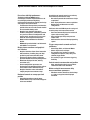
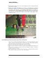
Agilent Infiniium 90000 X-Series Oscilloscopes at a Glance
Ease of use with high performance
The Agilent Infiniium 90000 X-Series
oscilloscopes combine unprecedented ease-ofuse with high-performance digitizing
oscilloscope functionality to simplify your design
and analysis measurement tasks.
• Traditional oscilloscope front-panel interface
provides direct access to the controls needed
for most troubleshooting tasks.
• Graphical user interface with menus,
windows, dialog boxes, and toolbars provides
easy access to dozens of configuration and
analysis tools, ensuring you can set up and
make the most complex measurements.
• Models with bandwidths from 13 GHz to
32 GHz.
• MSO models provide 10 GSa/s at 16 channels
and 20 GSa/s at 8 channels.
Display shows waveforms and graphical
user interface
•
•
•
•
•
Graphical interface allows direct interaction
with waveforms, including drag-and-drop
positioning and instant waveform zoom.
Touchscreen display allows oscilloscope
operation without an external pointing device.
Waveforms displayed in color, making
correlation easy.
Current configuration parameters are
displayed near the waveform display and are
color-coded to make identification easy.
Graphical interface menus and toolbars
simplify complex measurement setups.
Horizontal controls set sweep speed and
position
•
2
Intensified waveforms on main sweep
window make it easy to see what will appear
in the zoom window.
Acquisition and general controls start and stop
the oscilloscope and do basic setup
• Run and stop controls for continuous or single
acquisitions.
• Clear display before one or more acquisitions.
• Default setup and Autoscale set initial
configuration.
Solid state drive and USB 2.0 port for saving and
restoring setups and measurement results
• Store measurement displays for inclusion in
reports and test setup guides.
• Store oscilloscope setups to repeat tests
another time.
• Solid state drive stores oscilloscope operating
system.
Trigger setup controls set mode and basic
parameters
•
•
•
•
Select Edge, Glitch, or Advanced Modes.
Choose input source and slope.
Use graphical user interface to simplify
configuration of pattern, state, delay, and
violation trigger modes.
Use auxiliary trigger to increase triggering
flexibility.
Vertical controls set attenuation and position
•
Color-coded knobs make it easy to find the
controls that affect each waveform.
Marker and quick measurements help
measure waveform parameters
•
Waveform markers A and B to check voltage
or Δ-time at any point on the displayed
waveform.
In This Service Guide
This guide provides the service information for the Agilent Technologies 90000 X- Series
and 90000 L- Series oscilloscopes. It is divided into seven chapters.
Chapter 1, "General Information," describes which oscilloscope models are covered by
this guide, supplied accessories, and where to find the specifications for the 90000 XSeries / 90000 L- Series oscilloscopes.
Chapter 2, "Calibration," describes the types of calibrations, and how and when to run
the user calibration procedure.
Chapter 3, "Testing Performance," provides instructions for testing the oscilloscope to
verify that it performs according to specifications.
Chapter 4, "Troubleshooting," provides flowcharts and procedures for diagnosing
problems for assembly- level repair.
Chapter 5, "Replacing Assemblies," provides instructions for removing and replacing
assemblies in the oscilloscope.
Chapter 6, "Replaceable Parts," provides exploded parts diagrams and a list for ordering
replaceable parts.
Chapter 7, "Theory of Operation," describes the basic structure of the oscilloscope and
how its parts interact.
At the back of the book you will find safety notices.
3
4
1
Instruments covered by this service guide
Accessories supplied 7
Specifications and Characteristics 7
General Information
6
Instruments covered by this service guide
Oscilloscopes manufactured after the date this manual was released may be different
from those described in this manual. The release date of this manual is shown on the
title page. This manual will be revised when necessary.
If you have an oscilloscope that was manufactured after the release of this manual,
please check the Agilent Technologies website at www.agilent.com to see whether a
newer version of this manual is available.
The following 90000 X- Series and L- Series oscilloscopes are covered in this guide.
Oscilloscopes Covered by this Service Guide
Model
Bandwidth
MSOX/DSOX/DSAX91304A
13 GHz bandwidth
MSOX/DSOX/DSAX91604A
16 GHz bandwidth
MSOX/DSOX/DSAX92004A
20 GHz bandwidth
MSOX/DSOX/DSAX92504A
25 GHz bandwidth
MSOX/DSOX/DSAX92804A
28 GHz bandwidth
DSO/DSA93004L
30 GHz bandwidth
MSOX/DSOX/DSAX93204A
32 GHz bandwidth
The oscilloscope model can be identified by the product number on the front or
rear panel.
6
Chapter 1: General Information
Accessories supplied
Accessories supplied
The following accessories are supplied.
• Mouse
• Stylus
• Keyboard
• Accessory pouch
• Front panel cover
• Calibration cable
• Connector saver collars (qty 10)
• Connector savers (f- f) (qty 5)
• Power cord (see parts list in chapter 6 for country- dependent part number)
• ESD wrist strap
• Digital channels cable (MSO models only): Agilent part number N2815- 68701
• MSO calibrator board assembly (MSO models only): Agilent part number N2834- 68703
Specifications and Characteristics
The following table contains a partial list of specifications and characteristics for the
Agilent Infiniium 90000 X- Series oscilloscopes. For a full list of specifications and
characteristics, see the data sheets at www.agilent.com/find/90000x- series.
Specifications that are pertinent to each test are in the "Testing Performance" chapter.
Specifications are valid after a 30- minute warm- up period, and within ± 5° C from the
temperature at which the last self- calibration was performed.
Environment
Indoor use only.
Ambient
temperature
Operating 5 °C to +40 °C
Non-operating –40 °C to +65 °C
Humidity
Operating: up to 95% relative humidity (non-condensing) at +40 °C
Non-operating: up to 90% relative humidity at +65 °C
Altitude
Operating: up to 4,000 m (12,000 feet)
Non-operating: up to 15,300 meters (50,000 feet)
Installation/
Measurement
Category
Installation category: 2.
Measurement category: 1
Power Requirements
100-240 V, 47-63 Hz; 800 W for 4-channel models.
100-240 V, 50 Hz;100-208 V, 50/60 Hz; 800 W for 8-channel models.
Voltage Fluctuations
Note that the mains supply voltage fluctuations are not to exceed +/-10% of the
nominal supply voltage.
Pollution Degree
The Infiniium 90000 X-Series oscilloscopes may be operated in environments of
Pollution Degree 2.
7
Chapter 1: General Information
Specifications and Characteristics
Pollution Degree
Definitions
8
Pollution Degree 1: No pollution or only dry, non-conductive pollution occurs. The
pollution has no influence. Example: A clean room or climate-controlled office
environment.
Pollution Degree 2. Normally only dry non-conductive pollution occurs. Occasionally a
temporary conductivity caused by condensation may occur. Example: General indoor
environment.
Pollution Degree 3: Conductive pollution occurs, or dry, non-conductive pollution
occurs which becomes conductive due to condensation which is expected. Example:
Sheltered outdoor environment.
2
Running a Self Calibration
Calibration
11
Calibration
A calibration is simply an oscilloscope self- adjustment. The purpose of a calibration is
performance optimization.
There are three ways to calibrate an Infiniium oscilloscope:
• User mode, also known as normal mode, a normal calibration, user calibration, or
self calibration. User mode includes the minimum set of calibrations and is intended
to be run by oscilloscope users. The user must be logged in as an administrator to
run a self calibration. In user mode you may choose to run time scale calibrations
and interleave correction calibrations, though those selections default to not run and
they require additional equipment. A self calibration takes about 2 hours and 15
minutes.
• Service mode, also known as a service calibration. A service calibration is performed
only by Agilent Service Center technicians. In service mode the 50 Ohm input
resistance calibration is performed, in addition to everything calibrated in the normal
mode. The time scale and interleave correction calibrations are run by default, though
they can be turned off. Additional equipment is required to run a service calibration.
A service calibration takes about 2 hours and 30 minutes.
• Factory mode, also known as a factory calibration. A factory calibration includes the
full set of calibrations, including time scale and interleave correction, and other
calibrations. A factory calibration is normally performed once during production of
the oscilloscope. All of the calibration factors are stored into flash RAM on the
acquisition board so that the calibration factors determined by the factory calibration
are preserved even if the hard drive is replaced or reformatted.
10
Chapter 2: Calibration
Running a self calibration
Running a self calibration
Let the Oscilloscope Warm Up Before Adjusting
Warm up the oscilloscope for 30 minutes before starting the calibration procedure. Failure to allow warm
up may result in inaccurate calibration.
The self calibration uses signals generated in the oscilloscope to calibrate channel
sensitivity, offsets, and trigger parameters. There are three times we recommend
performing a self calibration:
• At least once a year.
• When you replace the hard drive.
• When the oscilloscope’s operating temperature (after the 30- minute warm- up period)
is more than ±5 °C different from that of the last calibration. Be sure to perform a
self calibration—even if one was recently performed—when environmental temperature
conditions cause the oscilloscope’s operating temperature to change, such as when
the oscilloscope is moved to a test rack or chamber.
Equipment Required
Equipment
Critical Specifications
Agilent Part Number
Connector savers (5 supplied
with oscilloscope)
3.5mm (f) to 3.5 mm (f)
Agilent 5061-5311 (for 20, 25, 28, 30,
and 32 GHz models)
Agilent 1250-3758 (for 13 GHz
and16 GHz models)
Cable assembly
50 Ohm characteristic impedance BNC
(m) connectors, 36 inches (91 cm) to 48
inches (122 cm) long
Agilent 8120-1840
Adapter
SMA(m) to BNC(f)
Agilent 1250-1200
Cable (supplied with
oscilloscope)
No substitute
Agilent 54916-61626
Digital channels cable (MSO
models only)
No substitute
Agilent N2815-68701
MSO calibrator (MSO models
only)
No substitute
Agilent N2834-68703
Calibration time
It will take approximately 2 hours and 15 minutes to run the self calibration on the oscilloscope, including
the time required to change cables from channel to channel.
1 Let the oscilloscope warm up before running the self calibration.
The self calibration should be done only after the oscilloscope has run for 30 minutes
at ambient temperature with the cover installed. Calibration of an oscilloscope that has
not warmed up may result in an inaccurate calibration.
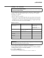
2 Select Utilities > Calibration.
3 Uncheck the Cal Memory Protect box.
You cannot run a self calibration if this box is checked. See Figure 2- 1.
11
Chapter 2: Calibration
Running a self calibration
Figure 2-1 Calibration Dialog Box
Clear this check
box before starting
calibration
Click here to start
calibration
4 Click Start, then follow the instructions on the screen.
The routine will ask you to do the following steps:
a Disconnect everything from all inputs and Cal Out.
b Indicate whether you want to run time scale and interleave correction calibrations.
For a list of equipment required to perform the time scale calibration, refer to
the “Time Scale Accuracy (TSA) Test” section in the next chapter. The interleave
correction calibration requires a sine wave generator and a ≥ 67 GHz cable with
1.85 mm male connectors on each end. You will also need to use the two supplied
1.85 mm (f)- (f) connector savers. To learn more about both calibration options,
click Help.
c Connect the calibration cable from Cal Out to channel 1.
You must use the 54916- 61626 cable assembly with two connector saver adapters
for all oscilloscopes. Failure to use the appropriate calibration cable will result
in an inaccurate calibration.
d Connect the calibration cable from Cal Out to each of the channel inputs as
requested.
e When instructed, connect the calibration cable from the Cal Out on the front
panel of the oscilloscope to the 1250- 1200 SMA(m) to BNC(f) adapter and then
connect the other end of the 1250- 1200 adapter to the 8120- 1840 BNC cable.
Connect the other end of the BNC cable to the Trig In on the rear of the
oscilloscope.
f A Passed/Failed indication appears for each calibration section. If any section
fails, click the Details box for information on the failures. Also check the
calibration cables.
5 If you are calibrating an MSO model oscilloscope, follow the prompts to connect the
digital channels cable to the digital channels connector on the rear of the oscilloscope
and to the calibration connector on the MSO calibrator.
CAUTION
Be sure to orient the digital channels cable with the Aglient part number facing
downward as shown on the rear of the oscilloscope. See Figure 2- 2.
12
Chapter 2: Calibration
Running a self calibration
Figure 2-2 Digital channels cable orientation
CAUTION
Insert the digital channels cable carefully into the MSO calibrator to prevent damage
to the pins. Use the notches on the cable and the MSO calibrator to orient the cable
correctly. See Figure 2- 3.
Figure 2-3 MSO calibrator
Alignment notches
6
After the calibration procedure is completed, click Close.
13
Chapter 2: Calibration
Running a self calibration
14
3
Vertical Performance Verification 17
Offset Accuracy Test 18
DC Gain Accuracy Test 25
Analog Bandwidth - - Maximum Frequency Test
Time Scale Accuracy (TSA) Test 37
Performance Test Record 39
Testing Performance
30
This section describes performance test procedures.
Performance Test Interval
The procedures in this section may be performed for incoming inspection and should
be performed periodically to verify that the oscilloscope is operating within specification.
The recommended test interval is once per year or after 2000 hours of operation.
Performance should also be tested after repairs or major upgrades.
Performance Test Record
A test record form is provided at the end of this section. This record lists performance
tests and test limits, and provides space to record test results.
Test Order
The tests in this section may be performed in any order. However, it is recommended
to conduct the tests in the order presented in this manual as this represents an
incremental approach to performance verification. This may be useful if you are
attempting to troubleshoot a suspected problem.
Test Equipment
Lists of equipment needed to conduct each test are provided for each test procedure.
The procedures are written to minimize the number and types of oscilloscopes and
accessories required. The oscilloscopes in these lists are ones that are currently available
for sale by Agilent at the time of writing this document. In some cases, the test
procedures use features specific to the oscilloscopes in the recommended equipment
list. However, the oscilloscopes, cables, and accessories that satisfy the critical
specifications in these lists may be substituted for the recommended models with some
modification to the test procedures.
Contact Agilent Technologies for more information about the Agilent products in these
lists.
16
Chapter 3: Testing Performance
Vertical Performance Verification
This section contains the following vertical performance verification tests:
•
•
•
•
Offset Accuracy Test
DC Gain Accuracy Test
Analog Bandwidth - - Maximum Frequency Test
Time Scale Accuracy (TSA) Test
17
Offset Accuracy Test
CAUTION
Ensure that the input voltage to the oscilloscope never exceeds ±5 V.
Let the oscilloscope warm up before testing.
The oscilloscope under test must be warmed up (with the oscilloscope application running) for at least
30 minutes prior to the start of any performance test.
Specifications
Offset Accuracy
≤ 3.5 V: ±(2% of channel offset + 1% of full scale + 1 mV)
> 3.5 V: ±(2% of channel offset + 1% of full scale)
Full scale is defined as 8 vertical divisions. Magnification is used below 10 mV/div. Below 10
mV/div, full scale is defined as 80 mV. The major scale settings are 10 mV, 20 mV, 50 mV, 100
mV, 200 mV, 500 mV and 1 V.
Equipment Required
Description
Critical Specifications
Recommended
Model/
Part Numbers
Digital Multimeter
DC voltage measurement accuracy better than ±0.1% of reading
Agilent 34401A or
Agilent 3458A
Cable Assembly
(2 required)
50Ω characteristic impedance, BNC (m) connectors
Agilent 8120-1840
Adapter
BNC Tee (m)(f)(f)
Agilent 1250-0781
Adapter
BNC (f) to dual banana
Agilent 1251-2277
Connector Saver
3.5 mm (f)-(f), shipped with each MSO/DSO/DSAX 90000A and
DSO/DSA93004L Series oscilloscope
Agilent 5061-5311 (used
with 20, 25, 28, 30, and 32
GHz oscilloscope
models)
Agilent 1250-3758 (used
with 13 GHz and 16 GHz
oscilloscope models)
Adapter
(2 required)
BNC (f) to SMA (m) adapter
Agilent 1250-1200
NOTE: The offset accuracy specification has two terms ±(offset gain + zero error). The
offset gain specification is ±2% of channel offset while the zero error specification is
±(1% of full scale + 1mV) for ≤ 3.5V and 1% of full scale for > 3.5V. The offset accuracy test
procedure tests each of these terms individually.
Zero Error Test Procedure
1 Disconnect all cables from the scope channel inputs.
2 Press [Default Setup], then configure the scope as follows:
a Select Setup > Acquisition.
18
Chapter 3: Testing Performance
Offset Accuracy Test
b When the Acquisition Setup window appears, enable averaging and set the # of
averages to 256 as shown below.
3 Filter out waveform noise by forcing the measurement calculations to wait until the
average is computed.
a Select Measure > Setup.
b Check the Wait for average to complete for measurements box.
c Click Close.
4 Configure the scope to measure Average voltage on channel 1 as follows:
a Change the vertical scale of channel 1 to 10 mV/div.
19
Chapter 3: Testing Performance
Offset Accuracy Test
b Click the V avg measurement on the left side of the screen.
V avg
measurement
c When the Enter Measurement Info window appears, ensure that the V avg function
is set up as follows and then click OK:
Source = Channel 1
Measurement Area = Entire Display
20
Chapter 3: Testing Performance
Offset Accuracy Test
5 Press [Clear Display] on the scope and wait for the #Avgs value (top right corner of
screen) to return to 256. Record the scope's mean V avg reading in the Zero Error Test
section of the Performance Test Record.
Notes
• For all scope readings in this procedure, use the mean value in the Measurements display area at the
bottom of the screen.
• If a question mark appears in front of any of the values at the bottom of the screen, press [Clear Display]
on the scope, wait for the #Avgs value to return to 256, and then record the scope reading.
Record the
mean reading
6 Change the vertical scale of channel 1 to 20 mV/div, press [Clear Display], wait for the
#Avgs value (top right corner of screen) to return to 256, and then record the scope
V avg reading in the Zero Error Test section of the Performance Test Record.
7 Repeat step 5 for the remaining vertical scale settings for channel 1 in the Zero Error
Test section of the Performance Test Record.
8 Press [Default Setup], then turn off channel 1 and turn channel 2 display on.
9 Configure the scope to measure V avg on Channel 2 as follows:
a Select Setup > Acquisition. When the Acquisition Setup window appears, enable
averaging and set the # of averages to 256.
b Change the vertical scale of channel 2 to 10 mV/div.
c Click the V avg measurement icon on the left side of the screen.
d When the Enter Measurement Info window appears, ensure that the Vavg function
is set up as follows and then click OK:
Source = Channel 2
Measurement area = Entire Display
10 Press [Clear Display] on the scope, wait for the #Avgs value to return to 256, and then
record the scope’s mean V avg reading in the Zero Error Test section of the Performance
Test Record.
11 Repeat step 9 for the remaining vertical scale settings for channel 2 in the Zero Error
section of the Performance Test Record.
12 Repeat steps 7 through 10 for channels 3 and 4.
21
Chapter 3: Testing Performance
Offset Accuracy Test
Offset Gain Test
1 Make the connections to scope channel 1 as shown below.
Connections
Cal Out on Oscilloscope Front Panel
Oscilloscope Channel Input
Connection Saver
Connection Saver
BNC (f) to SMA (m) adapter
BNC (f) to SMA (m) adapter
Notes:
• Where the BNC Tee adapter is used, it is important to connect it directly to the scope channel input
using the BNC (f) to SMA (m) adapter and the connection savers to minimize ground potential
differences and to ensure that the DMM measures the input voltage to the scope channel as accurately
as possible. Differences in ground potential can be a significant source of measurement error,
particularly at low voltage per division settings.
• It also helps to reduce ground potential differences if the scope and DMM are connected to the same
AC supply circuit.
• 256 averages are used in the scope measurements of this section to reduce measurement noise and to
reduce the measurement error due to resolution.
2 Set up the DMM to perform DC voltage measurements.
3 Configure the scope to measure V avg on Channel 1 as follows:
a Press [Default Setup].
b Select Setup > Acquisition. When the Acquisition Setup window appears, enable
averaging and set the # of averages to 256.
c Change the vertical scale of channel 1 to 10 mV/div.
d Click the V avg measurement icon on the left side of the screen.
22
Chapter 3: Testing Performance
Offset Accuracy Test
e When the Enter Measurement Info window appears, ensure that the V avg function
is set up as follows and then click OK:
Source = Channel 1
Measurement area = Entire Display
4 Set the channel 1 offset value to 400.0 mV by using the front panel control or:
a Pull down the Setup menu and select Channel 1 or click the Channel 1 setup icon.
b Click the Offset control arrows to change the offset value or click on the offset
value and enter 400.0 mV in the dialog box.
Channel 1
setup icon
5
Set the Cal Out voltage (VCal Out) to +400.0 mV as follows:
a Select Utilities > Calibration Output.
b Change the Signal Output function to DC (top left corner).
c Set the Level to 400.0 mV.
d Click Close.
6 Press [Clear Display] on the scope, wait for the #Avgs value (top right corner of screen)
to return to 256, and then record the DMM voltage reading as VDMM+ and the scope
Vavg reading as VScope+ in the Offset Gain Test section of the Performance Test Record.
23
Chapter 3: Testing Performance
Offset Accuracy Test
7 Change the channel 1 offset value to - 400.0 mV.
8 Set the Cal Out voltage to - 400.0 mV.
9 Press [Clear Display] on the scope, wait for the #Avgs value (top left corner of screen)
to return to 256, and then record the DMM voltage reading as VDMM- and the scope
Vavg reading as VScope- in the Offset Gain Test section of the Performance Test Record.
10 Change the channel 1 offset value to 0 mV.
11 Set the Cal Out voltage to 0 mV.
12 Press [Clear Display] on the scope, wait for the #Avgs value (top left corner of screen)
to return to 256, and then record the DMM voltage reading as VDMM0 and the scope
Vavg reading as VScope0 in the Offset Gain Test section of the Performance Test Record.
13 Calculate the offset gain error using the following expressions and record the value in
the Offset Gain Test section of the Performance Test Record. The offset gain error is
the greater (maximum magnitude) of either:
scope+ – V scope0
V
------------------------------------------ – 1 100
V DMM+ – V DMM0
or
scope- – V scope0
V
----------------------------------------- – 1 100
V DMM- – V DMM0
14 Repeat steps 4 to 13 for the remaining channel 1 vertical scale settings in the Offset
Gain Test section of the Performance Test Record. For each measurement, set both the
Cal Out voltage (VCal Out) and the Channel offset voltage to the positive VCal Out value
and then to the negative VCal Out value in the "VCal Out Setting" column of the Offset
Gain Test table in the Performance Test Record for each of the vertical scale settings.
15 Move the Tee connector to the next channel input and repeat steps 4 to 13 for channels
2 to 4.
24
Chapter 3: Testing Performance
DC Gain Accuracy Test
DC Gain Accuracy Test
CAUTION
Ensure that the input voltage to the oscilloscope never exceeds ±5 V.
Let the oscilloscope warm up before testing.
The oscilloscope under test must be warmed up (with the oscilloscope application running) for at least
30 minutes prior to the start of any performance test.
Specifications
DC Gain Accuracy
±2% of full scale at full resolution channel scale
Full scale is defined as 8 vertical divisions. Magnification is used below 10 mV/div. Below 10
mV/div full scale is defined as 80 mV. The major scale settings are 10 mV,
20 mV, 50 mV, 100 mV, 200 mV, 500 mV and 1 V.
Equipment Required
Description
Critical Specifications
Recommended
Model/
Part Numbers
Digital Multimeter
DC voltage measurement accuracy better than ±0.1% of reading
Agilent 34401A or
Agilent 3458A
Cable Assembly
(2 required)
50Ω characteristic impedance, BNC (m) connectors
Agilent 8120-1840
Adapter
BNC Tee (m)(f)(f)
Agilent 1250-0781
Adapter
BNC (f) to dual banana
Agilent 1251-2277
Connector Saver
3.5 mm (f)-(f), shipped with each MSO/DSO/DSAX 90000A and
DSO/DSA93004L Series oscilloscope
Agilent 5061-5311 (used
with 20, 25, 28, 30, and 32
GHz oscilloscope
models)
Agilent 1250-3758 (used
with 13 GHz and 16 GHz
oscilloscope models)
Adapter
(2 required)
BNC (f) to SMA (m) adapter
Agilent 1250-1200
25
Chapter 3: Testing Performance
DC Gain Accuracy Test
Procedure
1 Make the connections to scope channel 1 as shown below.
Connections
Cal Out on Oscilloscope Front Panel
Oscilloscope Channel Input
Connection Saver
Connection Saver
BNC (f) to SMA (m) adapter
BNC (f) to SMA (m) adapter
Notes:
• Where the BNC Tee adapter is used, it is important to connect it directly to the scope channel input
using the BNC (f) to SMA (m) adapter and the connection saver to minimize ground potential
differences and to ensure that the DMM measures the input voltage to the scope channel as accurately
as possible. Differences in ground potential can be a significant source of measurement error,
particularly at low voltage per division settings.
• It also helps to reduce ground potential differences if the scope and DMM are connected to the same
AC supply circuit.
• 256 averages are used in the scope measurements of this section to reduce measurement noise and to
reduce the measurement error due to resolution.
2 Press [Default Setup], then configure the scope as follows:
a Select Setup > Acquisition.
26
Chapter 3: Testing Performance
DC Gain Accuracy Test
b When the Acquisition Setup window appears, enable averaging and set the # of
averages to 256 as shown below.
3 Filter out waveform noise by forcing the measurement calculations to wait until the
average is computed.
a Select Measure > Setup.
b Check the Wait for average to complete for measurements box.
c Click Close.
4 Set the Cal Out voltage (VCal Out) to +30 mV as follows:
a Select Utilities > Calibration Output.
b Change the Signal Output function to DC (top left corner).
c Set the Level to 30 mV.
d Click Close.
27
Chapter 3: Testing Performance
DC Gain Accuracy Test
5 Set the channel 1 vertical scale value to 10 mV/div by using the front panel control or:
a Pull down the Setup menu and select Channel 1 or click the Channel 1 setup icon.
b Change the vertical scale of channel 1 to 10 mV/div.
c Select the Vavg measurement as shown below.
V avg
measurement
d When the Enter Measurement Info window appears, ensure that the V avg function
is set up as follows and then click OK:
Source = Channel 1
Measurement Area = Entire Display
6 Press [Clear Display] on the scope, wait for the #Avgs value (top right corner of screen)
to return to 256, and then record the scope's mean V avg reading in the DC Gain
Accuracy Test section of the Performance Test Record.
Notes
• For all scope readings in this procedure, use the mean value in the Measurements display area at the
bottom of the screen.
• If a question mark appears in front of any of the values at the bottom of the screen, press [Clear Display]
on the scope, wait for the #Avgs value to return to 256, and then record the scope reading.
28
Chapter 3: Testing Performance
DC Gain Accuracy Test
Record the
mean reading
7 Change the Cal Out voltage to - 30 mV.
8 Press [Clear Display] on the scope, wait for the #Avgs value to return to 256 and then
record the DMM voltage reading and the scope V avg reading in the DC Gain Test
section of the Performance Test Record.
9 Calculate the DC gain using the following expression and record this value in the DC
Gain Test section of the Performance Test Record.
For vertical scale setting of less than 1 volt use the following equation:
ΔV out
V scope+ – V scopeDCGainError = -------------- = ----------------------------------------- – 1 ⋅ 75
ΔV in V DMM+ – V DMM-
For vertical scale = 1 V use the following equation:
ΔV out
V scope+ – V scopeDCGainError = -------------- = ----------------------------------------- – 1 ⋅ 60
ΔV in V DMM+ – V DMM10 Repeat steps 3 to 8 for the remaining channel 1 vertical scale settings in the DC Gain
Test section of the Performance Test Record. For each measurement, set both the Cal
Out voltage (VCalOut) and the Channel offset voltage to the positive VCalOut value and
then to the negative VCalOut value in the “VCalOut Setting” column of the DC Gain Test
table in the Performance Test Record for each of the vertical scale settings used.
11 Move the Tee connector to the next channel input and repeat steps 3 to 9 for channels
2 to 4.
29
Chapter 3: Testing Performance
Analog Bandwidth -- Maximum Frequency Test
Analog Bandwidth - - Maximum Frequency Test
CAUTION
Ensure that the input voltage to the oscilloscope never exceeds ±5 V.
Let the oscilloscope warm up before testing.
The oscilloscope under test must be warmed up (with the oscilloscope application running) for at least
30 minutes prior to the start of any performance test.
Specification
Analog Bandwidth (-3 dB)
MSO/DSO/DSAX91304A
13.0 GHz
MSO/DSO/DSAX91604A
16.0 GHz
MSO/DSO/DSAX92004A
20.0 GHz
MSO/DSO/DSAX92504A
25.0 GHz
MSO/DSO/DSAX92804A
28.0 GHz
DSO/DSA93004L
30.0 GHz
MSO/DSO/DSAX93204A
32.0 GHz
Equipment Required
Description
Critical Specifications
Recommended Model/
Part Numbers
Microwave CW
Generator
Maximum Frequency ≥ 32 GHz
Power range: -20 dBm to +16 dBm into 50Ω
Output resistance = 50Ω
Agilent E8257D with Opt 540
Power Splitter
2 Resistor Power Splitter
Max Frequency ≥32 GHz
Agilent 11667C
Power Meter
Agilent E-series with power sensor compatibility
Agilent E4418B or E4419B
Power Sensor
Maximum Frequency ≥ 32 GHz
Power range: -24 dBm to +16 dBm
Agilent 8487A or Agilent E4413B
with 8485A-033
Microwave Cable
50Ω Characteristic Impedance
2.4 mm (m) to 2.4 mm (m) SMA connectors
Max Frequency ≥32 GHz
Agilent N5180-60204
Adapter
2.4 mm (m) to 3.5 mm (m) (qty. 1)
Agilent 11901A
Adapter
2.4 mm (m) to 3.5 mm (f) (qty. 2)
Agilent 11901C
Connector Saver
3.5 mm (f)-(f), shipped with MSO/DSO/DSAX 90000A
and DSO/DSA93004L models
Agilent 5061-5311 (used with 20,
25, 28, 30, and 32 GHz oscilloscope
models)
Agilent 1250-3758 (used with 13
and 16 GHz oscilloscope models)
30
Chapter 3: Testing Performance
Analog Bandwidth -- Maximum Frequency Test
Connections
Microwave CW
Generator E8257D
Power meter E4418A or
E4419A
Oscilloscope
Power splitter
11667C
Connection saver
Power sensor
cable
11901A adapter
Microwave cable
Power sensor
E4413A
11901C adapter
Notes
• Connect output 1 of the 11667C splitter to the scope Channel n input directly using the 11901A adapter
and a connector saver (either 5061-5311 or 1250-3758 depending on the oscilloscope’s bandwidth),
without any additional cabling or adapters.
• Connect the power sensor directly to output 2 of the power splitter using the 11901C adapter without
any additional cabling or adapters.
• Connect the microwave cable directly to output 3 of the power splitter using the 11901C adapter
without any additional cabling or adapters.
• Minimize the use of other adapters.
• Ensure that 2.4 mm and 3.5 mm connectors are tightened properly:
8 in-lbs (90 N-cm) for 3.5 mm
8 in-lbs (90 N-cm) for 2.4 mm
Procedure
1 Preset the power meter.
2 Ensure that the power sensor is disconnected from any source and zero the meter.
3 Connect the power sensor to the power meter's Power Ref connector and calibrate the
meter.
4 Make the connections to oscilloscope channel 1 as shown in the connection diagram
above.
5 Set up the Power Meter to display measurements in units of Watts.
6 Press [Default Setup], then configure the scope as follows:
a Ensure Channel 1 is displayed and all other channels are turned off.
b Set the vertical scale of channel 1 to 10 mV/div.
31
Chapter 3: Testing Performance
Analog Bandwidth -- Maximum Frequency Test
c Set the horizontal scale to 16 ns/div (to display 8 cycles of a 50 MHz waveform).
Click here and enter 16 ns
d Select Setup > Acquisition and then set up the acquisition parameters as follows:
Sin(x)/x Interpolation = Auto
Analog Averaging = Disabled
Analog Memory Depth = Automatic
Analog Sampling rate = 80 GSa/s (maximum)
e Select Measure > Voltage > V rms.
32
Chapter 3: Testing Performance
Analog Bandwidth -- Maximum Frequency Test
f When the Enter Measurement Info window appears, configure this measurement
as follows:
Source = Channel 1
Measurement Area = Entire Display
RMS Type = AC
7 Set the generator to apply a 50 MHz sine wave with a peak- to- peak amplitude of about
4 divisions.
• Use the following table to determine the approximate required signal amplitude.
The amplitude values in the table below are not absolutely required. If your
generator is unable to produce the recommended amplitude, then set the generator
to the highest value that does not produce a vertically clipped signal on the scope.
Table 3-1. Nominal Generator Amplitude Settings
Scope
Vertical Scale
Generator Signal
Amplitude (Vp-p)
Generator Signal
Amplitude (dBm)
10 mV/div
0.08
-18
20 mV/div
0.16
-12
50 mV/div
0.4
-4
100 mV/div
0.8
+2
200 mV/div
1.6
+8
500 mV/div
4.0
+16
1 V/div
6.3
+20
8 Measure the input power to the scope channel and convert this measurement to Volts
RMS using the expression:
V in =
P meas × 50Ω
For example, if the power meter reading is 4.0 μW, then Vin = (4.0*10- 6 * 50Ω)1/2 =
14.1 mVrms.
Record the RMS voltage in the Analog Bandwidth - Maximum Frequency Check section
of the Performance Test Record (Vin @ 50 MHz).
33
Chapter 3: Testing Performance
Analog Bandwidth -- Maximum Frequency Test
9 Press [Clear Display] on the scope and record the scope V rms reading in the Analog
Bandwidth - Maximum Frequency Check section of the Performance Test Record (Vout
@ 50 MHz).
Notes
• For all scope readings in this procedure, use the mean value in the Measurements display area at the
bottom of the screen.
Record the
mean reading
10 Calculate the reference gain as follows:
V out @50 MHz
Gain 50 MHz = ------------------------------V in @50 MHz
Record this value in the Calculated Gain @50 MHz column in the Analog Bandwidth Maximum Frequency Check section of the Performance Test Record.
34
Chapter 3: Testing Performance
Analog Bandwidth -- Maximum Frequency Test
11 Change the generator frequency to the maximum value for the model being tested as
shown in the table below. It is not necessary to adjust the signal amplitude at this
point in the procedure.
Setting
Model
MSO/DSO/DSAX
91304A
MSO/DSO/DSAX
91604A
MSO/DSO/DSAX
92004A
MSO/DSO/DSAX
92504A
Maximum
Frequency
13 GHz
16 GHz
20 GHz
25 GHz
Scope Time
Base Setting
50 ps/div
50 ps/div
50 ps/div
50 ps/div
Model
MSO/DSO/DSAX
92804A
DSO/DSA 93004L
MSO/DSO/DSAX
93204A
Maximum
Frequency
28 GHz
30 GHz
32 GHz
Scope Time
Base Setting
50 ps/div
50 ps/div
50 ps/div
12 Change the scope time base to the value for the model under test in the table above.
Click here and enter time
base value from table
13 Measure the input power to the scope channel at the maximum frequency and convert
this measurement to Volts RMS using the expression:
V in =
P meas × 50Ω
For example, if the power meter reading is 4.0 μW, then Vin = (4.0*10- 6 * 50Ω)1/2 =
14.1 mVrms.
Record the RMS voltage in the Analog Bandwidth - Maximum Frequency Check section
of the Performance Test Record (Vin @ Max Freq).
14 Press [Clear Display] on the scope and record the scope V rms reading in the Analog
Bandwidth - Maximum Frequency Check section of the Performance Test Record (Vout
@ Max Freq).
15 Calculate the gain at the maximum frequency using the expression:
Gain Max Freq = 20 log 10
( V out Max Freq ) ⁄ ( V in Max Freq )
-----------------------------------------------------------------------------Gain 50 MHz
For example, if (Vout @ Max Frequency) = 13.825 mV, (Vin @ Max Frequency) = 13.461
mV and Gain @ 50MHz = 1.0023, then:
13.825 mV ⁄ 13.461 mV
Gain Max Freq = 20 log 10 ------------------------------------------------------------- = 0.212 dB
1.0023
Record this value in the Calculated Gain @Max Freq column in the Analog Bandwidth
- Maximum Frequency Check section of the Performance Test Record. To pass this test,
this value must be greater than - 3.0 dB.
35
Chapter 3: Testing Performance
Analog Bandwidth -- Maximum Frequency Test
16 Change the scope setup as follows:
a Change the channel vertical scale to 20 mV/div.
b Reset the horizontal scale to 16 ns/div (to display 8 cycles of a 50 MHz waveform).
17 Change the generator output as follows:
a Reset the generator frequency to 50 MHz.
b Change the amplitude to the value suggested for this scale in Table 3- 1.
18 Repeat steps 8, 9, and 10 to measure the reference gain at 50 MHz for this scale.
19 Repeat steps 11, 12, 13, and 14 to measure the gain at maximum frequency for this scale.
20 Repeat steps 15 to 19 to complete measuring gains for remaining scale settings for
channel 1 in the Analog Bandwidth - Maximum Frequency Check section of the
Performance Test Record.
21 Move the splitter to channel 2 and change the scope configuration as follows:
• Ensure Channel 2 is displayed and all other channels are turned off.
• Set the vertical scale of channel 2 to 10 mV/div.
• Set the horizontal scale to 16 ns/div (to display 8 cycles of a 50 MHz waveform).
• Right click on the V rms measurement at the bottom of the screen. When the RMS
voltage measurement setup window appears, change the source from Channel 1 to
Channel 2.
22 Repeat steps 7 to 20 to complete measuring gains for channel 2.
23 Move the splitter to channel 3 and change the scope configuration as follows:
a Ensure Channel 3 is displayed and all other channels are turned off.
b Set the vertical scale of channel 3 to 10 mV/div.
c Set the horizontal scale to 16 ns/div (to display 8 cycles of a 50 MHz waveform).
d Click on the V rms measurement at the bottom of the screen and select Customize.
When the V rms setup window appears, change the source from Channel 2 to
Channel 3.
24 Repeat steps 7 to 20 to complete measuring gains for channel 3.
25 Move the splitter to channel 4 and change the scope configuration as follows.
a Ensure Channel 4 is displayed and all other channels are turned off.
b Set the vertical scale of channel 4 to 10 mV/div.
c Set the horizontal scale to 16 ns/div (to display 8 cycles of a 50 MHz waveform).
d Click on the V rms measurement at the bottom of the screen. When the V rms
setup window appears, change the source from Channel 3 to Channel 4.
26 Repeat steps 7 to 20 to complete measuring gains for channel 4.
36
Chapter 3: Testing Performance
Time Scale Accuracy (TSA) Test
Time Scale Accuracy (TSA) Test
This procedure verifies the maximum TSA specification for the oscilloscope.
Equipment Required
Equipment
Critical Specifications
Recommended Model/Part
Synthesized sine
wave source
Output Frequency: ≥ 10 MHz
Output Amplitude: 0 dBm
Frequency Resolution: 0.1 Hz
Agilent E8267D PSG
10 MHz frequency
reference
Output Frequency: 10 MHz
Absolute Frequency Error: < ±0.0275 ppm
Agilent 53132A opt. 012 frequency counter
RF cable
50 ohm characteristic impedance (no
substitute)
BNC (m) connectors
Max Frequency: ≥ 50 MHz
Agilent 8120-1840
Adapters, assorted
3.5 mm (f) to Precision BNC (m)
3.5 mm (f) to 3.5 mm (f)
Agilent 54855-67604
Agilent 83059B
37
Chapter 3: Testing Performance
Time Scale Accuracy (TSA) Test
Connections
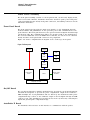
Connect the equipment as shown in the following figure.
1
2
3
4
5
6
7
8
9
10
11
12
13
14
15
Procedure
Configure the sine wave source to output a 0 dBm (600 mVpp) sine wave into 50 ohms
with a frequency of 10.00002000 MHz.
Adjust source amplitude such that displayed sine wave is 600 mVpp.
Press [Default Setup] on the oscilloscope.
Set channel 1's vertical scale to 100 mV/div.
Set the oscilloscope sample rate to 100 kSa/s.
Set the scope's horizontal scale to 20 ms/div.
Set the measurement thresholds for all waveforms to a fixed voltage level of 0 V and
±20 mV hysteresis. To do this, go under Measure > Thresholds in the top menu. Then
select Custom: level +/- Hysteresis and enter 20 mV into the Hysteresis field and 0
V into the Threshold Level field.
Enable a frequency measurement on channel 1.
On the oscilloscope, press [Stop].
Press [Clear Display].
Press [Run], wait until 10 acquisitions have accumulated, and then press [Stop].
Convert the average frequency value to time scale error by subtracting 20 Hz and
dividing by 10 Hz/ppm.
Record the time since calibration (in years) in the table. The calibration date can be
found in the Calibration menu window.
Calculate the test limits using the following formula and record them in the table.
Test Limits = ±(0.100 + 0.100 x Years Since Calibration)
Record the results in the Performance Test Record.
38
Chapter 3: Testing Performance
Performance Test Record
Performance Test Record
Agilent Technologies
Agilent 90000-X Series / 90000-L Series Oscilloscopes
Model Number _____________________
Tested by___________________
Serial Number ___________________________
Work Order No.___________________
Recommended Test Interval - 1 Year/2000 hours
Date___________________
Recommended next test date ___________________
Ambient temperature ___________________
Offset Accuracy Test
Zero Error Test
Vertical Scale
10 mV/div
20 mV/div
50 mV/div
100 mV/div
200 mV/div
500 mV/div
1 V/div
Test Limits
-1.8 mV to +1.8 mV
-2.6 mV to +2.6 mV
-5.0 mV to +5.0 mV
-9.0 mV to +9.0 mV
-17.0 mV to +17.0
mV
-41.0 mV to +41.0
mV
-81.0 mV to +81.0
mV
Channel 1
Channel 2
Channel 3
Channel 4
39
Chapter 3: Testing Performance
Performance Test Record
Offset Gain Test
Vertical
Scale
Channel 1
10 mV/div
20 mV/div
50 mV/div
100 mV/div
200 mV/div
500 mV/div
1 V/div
Channel 2
10 mV/div
20 mV/div
50 mV/div
100 mV/div
200 mV/div
500 mV/div
1 V/div
Channel 3
10 mV/div
20 mV/div
50 mV/div
100 mV/div
200 mV/div
500 mV/div
1 V/div
Channel 4
10 mV/div
20 mV/div
50 mV/div
100 mV/div
200 mV/div
500 mV/div
1 V/div
VCal Out
Setting
VDMM+
VDMM-
VDMM0
VScope+
VScope-
VScope0
Calculated
Offset Gain
Error
Offset Gain
Error Test
Limits
±400 mV
±400 mV
±700 mV
±1.2 V
±2.2 V
±2.4 V
±2.4 V
±2 %
±2 %
±2 %
±2 %
±2 %
±2 %
±2 %
±400 mV
±400 mV
±700 mV
±1.2 V
±2.2 V
±2.4 V
±2.4 V
±2 %
±2 %
±2 %
±2 %
±2 %
±2 %
±2 %
±400 mV
±400 mV
±700 mV
±1.2 V
±2.2 V
±2.4 V
±2.4 V
±2 %
±2 %
±2 %
±2 %
±2 %
±2 %
±2 %
±400 mV
±400 mV
±700 mV
±1.2 V
±2.2 V
±2.4 V
±2.4 V
±2 %
±2 %
±2 %
±2 %
±2 %
±2 %
±2 %
40
Chapter 3: Testing Performance
Performance Test Record
DC Gain Accuracy Test
Vertical Scale
Channel 1
10 mV/div
20 mV/div
50 mV/div
100 mV/div
200 mV/div
500 mV/div
1 V/div
Channel 2
10 mV/div
20 mV/div
50 mV/div
100 mV/div
200 mV/div
500 mV/div
1 V/div
Channel 3
10 mV/div
20 mV/div
50 mV/div
100 mV/div
200 mV/div
500 mV/div
1 V/div
Channel 4
10 mV/div
20 mV/div
50 mV/div
100 mV/div
200 mV/div
500 mV/div
1 V/div
VCal Out
Setting
VDMM+
VDMM-
VScope+
VScope-
Calculated
DC Gain
Error
DC Gain Error
Test Limits
±30 mV
±60 mV
±150 mV
±300 mV
±600 mV
±1.5 V
±2.4 V
±2 %
±2 %
±2 %
±2 %
±2 %
±2 %
±2 %
±30 mV
±60 mV
±150 mV
±300 mV
±600 mV
±1.5 V
±2.4 V
±2 %
±2 %
±2 %
±2 %
±2 %
±2 %
±2 %
±30 mV
±60 mV
±150 mV
±300 mV
±600 mV
±1.5 V
±2.4 V
±2 %
±2 %
±2 %
±2 %
±2 %
±2 %
±2 %
±30 mV
±60 mV
±150 mV
±300 mV
±600 mV
±1.5 V
±2.4 V
±2 %
±2 %
±2 %
±2 %
±2 %
±2 %
±2 %
41
Chapter 3: Testing Performance
Performance Test Record
Analog Bandwidth - Maximum Frequency Check
Max frequency:
MSO/DSO/DSAX91304A = 13 GHz, MSO/DSO/DSAX91604A = 16 GHz, MSO/DSO/DSAX92004A = 20 GHz,
MSO/DSO/DSAX92504A = 25 GHz, MSO/DSO/DSAX92804A = 28 GHz, DSO/DSA93004L = 30 GHz, MSO/DSO/DSAX93204A = 32 GHz .
Measurement
Vin @ 50 MHz
Vout @ 50
Calculated
Vin @ Max
Vout @ Max
Calculated
Vertical Scale
MHz
Gain @ 50
Freq
Freq
Gain @ Max
MHz
Freq
(Test Limit =
(Test Limit =
greater than greater than 3 dB)
3 dB)
Channel 1
10 mV/div
20 mV/div
50 mV/div
100 mV/div
200 mV/div
500 mV/div
1 V/div
Channel 2
10 mV/div
20 mV/div
50 mV/div
100 mV/div
200 mV/div
500 mV/div
1 V/div
Channel 3
10 mV/div
20 mV/div
50 mV/div
100 mV/div
200 mV/div
500 mV/div
1 V/div
Channel 4
10 mV/div
20 mV/div
50 mV/div
100 mV/div
200 mV/div
500 mV/div
1 V/div
42
Time Scale Accuracy
Measured Time Scale
Error (ppm)
Years Since Calibration
(years)
Low Test Limit (ppm)
High Test Limit (ppm)
Pass/Fail
___________
___________
___________
___________
___________
43
Chapter 3: Testing Performance
Performance Test Record
44
4
Primary Trouble Isolation 47
Power Supply Troubleshooting 51
Setting Up the BIOS 62
Motherboard Verification 63
Display Troubleshooting 64
Acquisition/Backplane Assembly Troubleshooting
Keyboard Troubleshooting 67
LED Troubleshooting 68
Touch Screen Troubleshooting 69
Checking Probe Power Outputs 70
MSO Assembly Troubleshooting 71
Before You Contact Agilent 73
Troubleshooting
66
Troubleshooting
The service strategy for troubleshooting Agilent 90000 Series oscilloscopes is to isolate
problems to a faulty assembly, then use the disassembly and assembly procedures in
the "Replacing Assemblies" chapter to replace the defective assembly.
Read the Safety Notices at the back of this guide before servicing the oscilloscope.
Before performing any procedure, review any cautions and warnings included in the
procedures.
The only equipment you need for troubleshooting to the assembly level is basic electronic
troubleshooting tools such as a digital multimeter. If you need to remove and replace
any assembly, refer to the "Replacing Assemblies" chapter.
A Default Setup is provided to return the oscilloscope to a known state. You can use
the default setup to undo previous setups so they do not interfere with the current
measurement. Use the default setup when a procedure requires it. Press [Default Setup]
on the front panel to set the oscilloscope to the default state.
WARNING
INJURY CAN RESULT! Use caution when working around the cooling fans with the
cover removed from the oscilloscope. The cooling fan blades are exposed on one side
and can be hazardous. If the procedure allows, replace the cover over the chassis
(without screwing it back in place) before turning the oscilloscope on. If the procedure
requires you to have the cover off, be careful not to let these fan blades come in contact
with any part of your body.
CAUTION
AVOID ESD DAMAGE TO COMPONENTS! ELECTROSTATIC DISCHARGE (ESD) can
damage electronic components. Use proper ESD precautions when doing any of the
procedures in this chapter. Failure to follow proper ESD procedures may cause
immediate failure or latent damage. Latent damage may result in equipment failure
after a period of time. As a minimum, place the oscilloscope on a properly grounded
ESD mat and wear a properly grounded ESD strap.
WARNING
SHOCK HAZARD!
Maintenance should be performed by trained service personnel aware of the hazards
involved (for example, moving parts, fire, and electric shock). Lack of training and
awareness of the hazards could result in electrical shock or other injury. When
maintenance can be performed without power applied, the power cord should be removed
from the oscilloscope.
46
Chapter 4: Troubleshooting
Primary Trouble Isolation
Primary Trouble Isolation
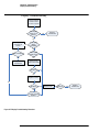
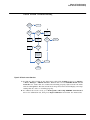
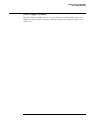
The main procedural tool in this chapter is the flowchart. The Primary Trouble Isolation
flowchart in Figure 4- 1 shows the entire troubleshooting path from a failed oscilloscope
to a working one, and directs you to other sections in this chapter where the procedures
are described in detail. Reference letters on the flowcharts in this chapter point to
procedural steps that explain the brief instructions in the flowchart.
$
3HUIRUP3RZHU8S
'RHVV\VWHP
VWD\RQ2."
1R
*RWR³3RZHU
6XSSO\
7URXEOHVKRRWLQJ´
1R
*RWR³'LVSOD\
7URXEOHVKRRWLQJ´
<HV
%
&KHFNGLVSOD\
,VGLVSOD\RQ
VFUHHQ"
<HV
&
5XQVFRSHVHOI
WHVWV
'RVHOIWHVWV
SDVV"
1R
*RWR³$FTXLVLWLRQ
%DFNSODQH$VVHPEO\
7URXEOHVKRRWLQJ´
<HV
'
5XQNH\ERDUGDQG
/('VHOIWHVWV
'RHVNH\ERDUG
ZRUN2."
1R
*RWR³.H\ERDUG
7URXEOHVKRRWLQJ´
1R
*RWR³/('
7URXEOHVKRRWLQJ´
'RHVWRXFK
VFUHHQZRUN
2."
1R
*RWR³7RXFK
6FUHHQ
7URXEOHVKRRWLQJ´
'RSUREHV
ZRUN2."
1R
*RWR³&KHFNLQJ
3UREH3RZHU
2XWSXWV´
<HV
'R/('VZRUN
2."
<HV
(
5XQDVHOIFDO
'RHVVHOIFDO
SDVV"
1R
*RWRSURFHGXUDOVWHS
³(6HOI&DOLEUDWLRQ´LQ
WKLVVHFWLRQ
<HV
)
6\VWHPZRUNV
5XQSHUIRUPDQFH
WHVWV
Figure 4-1 Primary Trouble Isolation Flowchart
47
Chapter 4: Troubleshooting
Primary Trouble Isolation
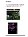
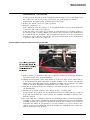
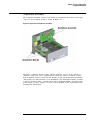
A Perform power- up.
Connect the oscilloscope power cord and press the power button in the lower left corner
of the front panel. If the oscilloscope is working properly, it will take several minutes
to start up and the graticule will appear on the screen. The exact appearance may look
slightly different than shown in Figure 4- 2, depending on the setup selected before the
oscilloscope was turned off.
Figure 4-2 Power-on display
If the oscilloscope turns off without you pressing the front panel power button, go to
the “Power Supply Troubleshooting” section of this chapter.
If the oscilloscope does not start up at all, unplug the oscilloscope, wait 30 seconds,
plug the oscilloscope back in, and turn the power on. If it still does not start up, go
to the “Setting Up the BIOS” and “Motherboard Verification” sections of this chapter.
B Check the display.
If the screen is black or has a scrambled display, go to the “Display Troubleshooting”
section of this chapter.
If the display shows MEMCON1, MEMCON2, MEMCON3, or MEMCON4 errors during
boot- up of the oscilloscope software, the lower acquisition board is faulty and requires
replacement. MEMCON5, MEMCON6, MEMCON7, and MEMCON8 errors indicate the
upper acquisition board is faulty and requires replacement.
C Run the oscilloscope self- tests.
1 Select Self Test from the Utilities menu.
2 Select Scope Self Test from the Self Test drop- down list box.
3 Click Start Test and follow the instructions on the screen.
If any of the self tests fail, go to the “Acquisition/Backplane Assembly Troubleshooting”
section of this chapter for further troubleshooting.
D Check the front panel response by running the Keyboard and LED self tests.
Follow these steps to verify correct keyboard operation.
1 Select Self Test from the Utilities menu.
2 Select Keyboard Test from the Self Test drop- down list box, then click Start Test.
48
Chapter 4: Troubleshooting
Primary Trouble Isolation
The Front Panel Keyboard Test window appears with a symbolic representation of the
keyboard. See Figure 4- 3.
When you press a key
or turn a knob in both
directions, the
corresponding symbol
on this screen turns
green.
Figure 4-3 Knob and key self test screen
3 Press each key on the keyboard until you have pressed all keys. When you press
a key or push a knob, the bar above the corresponding key/knob symbol on the
display should change from red to green.
4 Turn each knob in both directions until you have turned all knobs. When you
turn a knob in one direction, half the rotation arrow under the corresponding
knob symbol should turn green. When you then turn the knob in the other
direction, the entire rotation arrow under the knob symbol should turn green.
5 When you are finished, click Close.
6 If any of the knobs or keys do not work, go to “Keyboard Troubleshooting” later
in this chapter.
Follow these steps to test the front panel LED (light- emitting diode) indicators.
1 Select Self Test from the Utilities menu.
2 Select LED Test from the Self Test drop- down list box, then click Start Test.
The Front Panel LED Test screen appears, showing a symbolic representation of all
front panel LED indicators. See Figure 4- 4.
49
Chapter 4: Troubleshooting
Primary Trouble Isolation
Figure 4-4 LED test screen
3 Repeatedly press [Single] on the front panel to step through and highlight each
LED symbol in the test screen. You can also step through the LEDs by pressing
the << Prev or Next >> buttons on the screen. Verify that the corresponding
LEDs on the front panel are the only ones illuminated. Additionally, pressing
the Multi- purpose button on the front panel will illuminate all the LEDs, and
pressing the Clear Display button on the front panel will turn off all the LEDs.
4 When you are finished, click Close.
5 If any of the LEDs do not work, go to “LED Troubleshooting” later in this chapter.
6 If both tests pass, make sure the touch screen and probes work properly and
then go to step E.
E Run a self calibration.
1 Complete a self calibration by following the procedures in chapter 2.
2 If the calibration test fails, look at the details to find the channel associated with
the fail.
• If the failure is associated with channel 1, look at the specific calibration that
failed. If it was a trigger cal, a timebase cal, or an interpolator gain cal, replace
the backplane board because it is likely the problem. If the cal still fails, replace
the lower acquisition board.
• If the failure is associated with channel 1 but is not a trigger cal, a timebase
cal, or an interpolator gain cal, replace the lower acquisition board. If the cal
still fails, replace the backplane board.
• If the failure is not associated with channel 1, replace the acquisition board
associated with that channel (channels 1 and 2 - lower acquisition board,
channels 3 and 4 - upper acquisition board).
• If all four channels have cal failures, the problem may be with the calibrator
located on the backplane board, so replace that board first. If the calibration
test passes, go to step F.
F The system is operational. Verify that the oscilloscope meets all warranted specifications
by following the procedures in the “Testing Performance” chapter.
50
Chapter 4: Troubleshooting
Power Supply Troubleshooting
Power Supply Troubleshooting
This section provides information to help you isolate the problem to the assembly level
when the power system is not operating.
There are three main types of faults:
• Under- voltage faults
• Over- temperature faults
• Over- voltage faults
To determine what type of fault is occurring, and what assembly needs to be replaced,
follow these steps:
1 Unplug the oscilloscope so the +5V standby power supply can fully discharge.
2 Wait 30 seconds.
3 Plug the oscilloscope back in.
4 Wait 5 seconds.
5 Press the front panel power button and count how many seconds it takes for
the oscilloscope to lose power again. Keep the oscilloscope plugged in when it
loses power.
• If it takes about 2 seconds for the oscilloscope to lose power, you likely have
an under- voltage fault.
• If it takes 4 seconds or more for the oscilloscope to lose power, you likely
have an over- temperature fault.
• If the oscilloscope never powers up, or flickers then shuts off immediately,
you likely have an over- voltage fault or a defective bulk +12V power supply.
There are two sets of LEDs on the backplane assembly and one set on each acquisition
assembly. Seeing which of these LEDs are illuminated will help you identify the reason
for the power failure.
WARNING
SHOCK HAZARD!
The maintenance described in this section is performed with power supplied to the
oscilloscope and with the protective covers removed. Only trained service personnel
who are aware of the hazards involved should perform the maintenance. Read the safety
notices at the back of this guide before proceeding. Failure to observe safety precautions
may result in electric shock.
WARNING
SHOCK HAZARD!
Once the bulk +12V power supply is removed from the oscilloscope, two AC leads
located on the supply are exposed and severe shock can result if touched. Extreme care
should be taken to avoid contact with these leads when removing or testing the bulk
+12V power supply.
51
Chapter 4: Troubleshooting
Power Supply Troubleshooting
To locate all four sets of LEDs, remove the handle, outer oscilloscope cover, and inner
top cover to expose the motherboard cavity and top edges of the backplane assembly.
The first set of LEDs is located in the upper right corner of the backplane assembly
(see Figure 4- 5). Six of the LEDs indicate an under- voltage fault, and four indicate an
over- temperature fault. Another LED in this group is BULK SUPPLY FAIL, located
below NEG SUPPLY FAIL. It lights up if the bulk supply needs replacing.
Figure 4-5 Under-voltage, over-temperature, and bulk supply indicator LEDs on backplane assembly
52
Chapter 4: Troubleshooting
Power Supply Troubleshooting
The other three groups of LEDs indicate over- voltage faults. One group is located near
the center of the top edge of the backplane assembly just above the blue and red SATA
cables (see Figure 4- 6).
Figure 4-6 Over-voltage indicator LEDs on backplane assembly
If any of these LEDs are lit, the backplane assembly must be replaced.
53
Chapter 4: Troubleshooting
Power Supply Troubleshooting
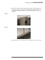
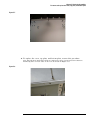
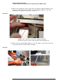
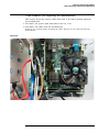
Locate the other two groups of over- voltage fault LEDs along the edges of the two
acquisition assemblies. They are visible through the bottom fan opening located on the
left side of the oscilloscope, nearest the rear panel (see Figure 4- 7 and Figure 4- 8).
Figure 4-7 Over-voltage indicator LEDs on acquisition assembly behind fan
Figure 4- 8 shows the fan opening with the fan removed. You do not need to remove
the fan to diagnose a problem; you can see the LEDs through the fan.
Figure 4-8 Over-voltage indicator LEDs with fan removed
The acquisition assembly nearest the bottom of the oscilloscope is the channels 1 and
2 acquisition assembly (LOWER ACQ) and the one above it is the channels 3 and 4
acquisition assembly (UPPER ACQ). If you look through the fan and see any of the
over- voltage LEDs lit, that acquisition assembly needs to be replaced.
54
Chapter 4: Troubleshooting
Power Supply Troubleshooting
The following table shows each LED, the type of fault it indicates, and what to do if
that LED indicator is illuminated.
LED
Type of Fault
What To Do
Group of 11 LEDs on Backplane Assembly
L-ACQ TEMP FAIL
Over-temperature
Go to “If the L-ACQ TEMP FAIL
or U-ACQ TEMP FAIL LED is Lit”
L-ACQ SUPPLY FAIL
Under-voltage
Replace channels 1 and 2
acquisition assembly (LOWER
ACQ)
FP SUPPLY FAIL
Under-voltage
Go to “If the FP SUPPLY FAIL
LED is Lit”
U-ACQ SUPPLY FAIL
Under-voltage
Replace channels 3 and 4
acquisition assembly (UPPER
ACQ)
FPGA SUPPLY FAIL
Under-voltage
Replace backplane assembly
NEG SUPPLY FAIL
Under-voltage
Replace backplane assembly
U-ACQ TEMP FAIL
Over-temperature
Go to “If the L-ACQ TEMP FAIL
or U-ACQ TEMP FAIL LED is Lit”
MAIN FAN FAIL
Over-temperature
Go to “If the MAIN FAN FAIL
LED is Lit”
PRED FAN FAIL
Over-temperature
Go to “If the PRED FAN FAIL
LED is Lit”
BP POL FAIL
Under-voltage
Replace backplane assembly
BULK SUPPLY FAIL
Replace bulk supply
Group of 7 LEDs on Backplane Assembly
FPGA +1.2V
Over-voltage
Replace backplane assembly
FPGA +1.8V
Over-voltage
Replace backplane assembly
FPGA +2.5V
Over-voltage
Replace backplane assembly
+3.3V POL
Over-voltage
Replace backplane assembly
FPGA +3.3V
Over-voltage
Replace backplane assembly
+5V POL
Over-voltage
Replace backplane assembly
ADC_VDO POL
Over-voltage
Replace backplane assembly
LEDs on Each Acquisition Board
U1101 oV
Over-voltage
Replace acquisition assembly
U303L oV
Over-voltage
Replace acquisition assembly
U1600 oV
Over-voltage
Replace acquisition assembly
U1100 oV
Over-voltage
Replace acquisition assembly
U300 3.3V oV
Over-voltage
Replace acquisition assembly
U300 2.5V oV
Over-voltage
Replace acquisition assembly
U303R oV
Over-voltage
Replace acquisition assembly
U1601 oV
Over-voltage
Replace acquisition assembly
55
Chapter 4: Troubleshooting
Power Supply Troubleshooting
If the FP SUPPLY FAIL LED is Lit
If the FP SUPPLY FAIL LED is the only one lit, there might be a problem with one of
the supplies that goes to the front panel assembly, or a problem on the front panel
assembly. Unplug the front panel power connector (see cable connector circled in Figure
4- 9) and turn the oscilloscope on again. If no other under- voltage indicator LEDs on
the backplane assembly turn on, the fault is on the front panel assembly and it should
be replaced. If either the BP POL FAIL or NEG SUPPLY FAIL LEDs turn on, then
replace the backplane assembly and confirm that the fault goes away with the front
panel power reconnected to the backplane assembly.
Figure 4-9 Front Panel Power Cable Connector
If the oscilloscope turns off again and no under- voltage fault indicator LEDs are lit,
the bulk +12V supply may be defective and may need to be replaced.
Be sure to verify the operation of the AC OK and DC OK signals first. The AC OK
signal indicates that the applied AC signal is within the specified input range (TTL high
logic level indicates that AC input is good). It is possible for this signal to indicate that
the AC input is not within the requested range even though it is correct. The DC OK
signal indicates whether the main output from the supply (+12.6V) is good (TTL high
logic level indicates the DC output is good). It is possible for this output to be false
even though the supply output is correct.
It is also possible that there is a short circuit on the bulk +12V supply trace somewhere
in the system, which would also cause the unit not to power on. If so, you need to
isolate the assembly that is shorted. You do not need to remove the acquisition or
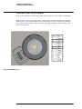
backplane assemblies to perform the following steps.
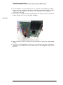
1 With the power turned off, disconnect the bulk +12V supply (see Figure 4- 10), but do
not remove the supply from the oscilloscope.
2 On the backplane assembly, measure the resistance across the FET (Q1409, located in
the upper right corner of the backplane) between +12V and ground as shown in Figure
4- 13, or measure the resistance across the bulk supply input pins on the backplane
assembly. Make sure the red lead is plugged into the HI output and the black lead is
56
Chapter 4: Troubleshooting
Power Supply Troubleshooting
3
4
5
6
plugged into the LO or COMMON input of the DVM. On a good backplane assembly,
you should measure about 700 ohms. If there is a short on this board, you would
measure something very near 0 ohms.
If there is a short, disconnect the power cable to the front panel (see Figure 4- 9) and
redo the resistance measurement.
If the short is gone, replace the front panel assembly and verify that the oscilloscope
now powers on.
If there is still a short circuit, disconnect the two large connectors that provide power
to the motherboard (J1201 and J1202) from the backplane assembly (see the circled
cable connections in Figure 4- 11) and redo the resistance measurements across the
FET (Q1409) or the bulk supply input pins on the backplane assembly.
If the short is gone, replace the motherboard assembly and confirm that the unit will
power on.
Figure 4-10 Power supply disconnect
Figure 4-11 Cable connection into backplane
57
Chapter 4: Troubleshooting
Power Supply Troubleshooting
7 If there is still a short circuit, remove both acquisition boards and unplug them from
the backplane assembly.
8 Measure each assembly individually to see if there is a short between the +12V trace
and ground (see Figure 4- 12). You should see a resistance of about 2000 ohms between
the +12V trace and ground on a good acquisition assembly. Make sure you make the
measurement using a DVM with the red lead plugged into the HI input and the black
lead plugged into the LO or COMMON input of the DVM. If there is a short between
these two traces, the reading you get will be very low (near 0 ohms). Replace either
assembly if needed.
Figure 4-12 Measuring the acquisition assembly resistance between +12V and ground
1
2
3
4
If no shorts are found on the bulk +12V supply trace or if you have fixed all the shorts
and the oscilloscope still will not turn on, follow these steps, which include replacing
parts with known good parts until you discover the problem.
Replace the bulk +12V power supply with a known good supply.
If the oscilloscope still does not power on, replace the motherboard with a known good
one.
If the oscilloscope still does not power on, then the backplane assembly is causing the
problem and must be replaced.
Once the faulty board or switch is discovered, be sure to reinstall all other parts that
were removed, as they were not the cause of the problem.
58
Chapter 4: Troubleshooting
Power Supply Troubleshooting
Figure 4-13 Measuring the backplane assembly resistance between +12V and ground across Q1409.
If the MAIN FAN FAIL LED is Lit
If the MAIN FAN FAIL LED is lit, the problem is a cooling system failure.
Four fans are located on the left side of the oscilloscope to cool it. It is possible that
the circuitry that generates the reference potential for the fans has failed. This circuitry
failure would cause the fans to stop turning and the oscilloscope to shut down.
It is unlikely that all four case fans would become faulty simultaneously and stop
turning. It is more likely that the high side drive circuitry for the case fans failed.
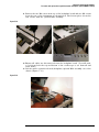
Follow these steps to diagnose a main fan failure:
1 Reset the sensing and shutdown logic by removing the AC power until the green LED
on the motherboard goes out (or just wait 30 seconds).
2 Move around to the left side of the oscilloscope so you can see the case fans (Figure 4- 14).
59
Chapter 4: Troubleshooting
Power Supply Troubleshooting
Figure 4-14 Case fans
3 Apply AC power to the oscilloscope and turn it on if it does not start up automatically.
Visually check to see if any of the fans are not turning. If none of the fans are turning,
it is likely a problem with the high side drive circuitry for the case fans. In that case,
you would replace the backplane assembly.
If any of the fans are turning, then they are probably not the cause of your shutdown
problem. (You should still replace any fans that are not turning, however.)
WARNING
INJURY CAN RESULT!
The following procedure requires you to touch fan hubs with objects or to use objects
to stop the fan blades from moving. Use caution when working near the cooling fans
with the covers removed from the oscilloscope. The cooling fan blades are exposed on
one side and can be hazardous. Be careful not to touch the moving fan blades with
any part of your body.
If the oscilloscope still shuts down, follow these steps:
1 Replace all the case fans.
2 Reset the logic by removing AC power for 30 seconds and make all of the case fans
so they cannot rotate. For example, have two people hold the four fan hubs or insert
an object between the blades of each of the fans.
3 Power the oscilloscope back on. If it shuts down again, the fan sensing and shutdown
function is operating properly. Replace the backplane.
If the PRED FAN FAIL LED is Lit
In addition to four case fans, there is also a single fan attached to the backplane
assembly that cools the trigger ICs. It is possible that this fan failed, or that the rotation
sensor for the fan failed. This sensor lets the oscilloscope know that the fan is turning.
If the sensor is faulty, the oscilloscope may think the fan is not working when it actually
is.
If the PRED FAN FAIL indicator LED on the backplane assembly is lit, the system
thinks there is a trigger ICs fan failure. To check, reset the sensing and shutdown logic
by removing the AC power until the green LED on the motherboard goes out (or just
wait 30 seconds). Then position yourself so you can see the trigger ICs fan on the
backplane assembly. Because this fan is on the bottom of the backplane it is somewhat
hidden by the acquisition assembly. Look down the backplane board to see it from
above. (See Figure 4- 15.)
60
Chapter 4: Troubleshooting
Power Supply Troubleshooting
Figure 4-15 Trigger ICs fan on backplane assembly
Apply AC power and turn the oscilloscope on if it does not start up on its own. Notice
whether the trigger ICs fan is turning. If it is not, replace it and redo this part of the
diagnostic test. If it is turning and the oscilloscope still turns off again, then consider
these possibilities:
• If the trigger ICs fan was turning, the problem is most likely that the rotation sensor
on the ICs fan is defective. Replace the trigger ICs fan and redo this part of the
diagnostic test.
• If the oscilloscope stays on after you reset the shutdown logic (by removing AC power
for 30 seconds) and powered it back on, then you have fixed the shutdown problem.
• If the oscilloscope shuts down again after you have replaced the trigger ICs fan, then
the problem could be that the rotation sensor for all the fans located on the backplane
assembly failed, so replace the backplane assembly and redo this part of the diagnostic
test.
If the L- ACQ TEMP FAIL or U- ACQ TEMP FAIL LED is Lit
If the oscilloscope shuts down and either the L- ACQ TEMP FAIL or U- ACQ TEMP FAIL
indicator LEDs is lit, then one of the scope channels is getting too hot or the temperature
sensing circuitry has failed. Normally, you would have to turn the oscilloscope on and
leave it on for awhile before you would see a shutdown caused by temperature problems.
If all the fans are turning, it is unlikely that the oscilloscope would shut down due to
temperature unless the airflow is being restricted or the input air is already too hot
to cool the insides of the oscilloscope.
It is possible that all the case fans and the trigger ICs are working, but the oscilloscope
still shuts down because of temperature due to one or more of the channels
malfunctioning and drawing too much current. If so, you would need to replace the
indicated acquisition assembly. It is also possible for one of the heat sinks on one of
the acquisition assemblies' critical parts to become detached and cause that part to
overheat and shut down the oscilloscope.
61
Chapter 4: Troubleshooting
Setting Up the BIOS
Setting Up the BIOS
If the BIOS settings become corrupt, the Infiniium oscilloscope PC motherboard will
not recognize the hard drive and the oscilloscope may not start. To configure the
motherboard BIOS parameters to the default settings, follow these steps:
1 Connect the power cable to the oscilloscope.
2 Connect the external keyboard to the rear panel.
3 Press Delete when the following prompt appears on the bottom of the screen:
Press TAB to show POST screen, DEL to Enter SETUP, F11 to Boot Menu.
If the prompt does not appear, or the oscilloscope does not appear to be functioning,
check the ribbon cable connectors. Otherwise, continue with the next step.
4 Go to Load Optimal Defaults and press Enter for optimized values, or go to Load
Failsafe Defaults and press Enter for fail- safe values. Select OK to load the defaults,
then press Enter.
5 Go to the Save and Exit Setup option and press Enter to save and exit the setup.Select
Y to save and exit, then press Enter.
62
Chapter 4: Troubleshooting
Motherboard Verification
Motherboard Verification
If you have been through the Power Supply Troubleshooting section of this chapter and
the oscilloscope still does not stay powered up, the problem may be with the
motherboard. To diagnose this problem, follow these steps.
1 Remove the handle, outer case, and top shield.
2 Turn the oscilloscope on.
If the unit beeps once after about 5 to 10 seconds but fails to boot up, the motherboard
is defective and needs to be replaced.
If the unit fails to beep after it is powered on, then measure the potential relative to
the chassis at pin 9 of J1201 (Figure 4- 16). Pin 9 is the reset line for the motherboard.
It is controlled by the backplane. You should measure about 3.3V. If the potential you
measure is correct, but the unit still has not beeped and started up, the motherboard
is defective and needs to be replaced.
Figure 4-16 Measure potential relative to chassis at pin 9 of J1201
3 If the potential you measure is not correct, shut the oscilloscope down and unplug the
AC cord from the rear of the instrument.
4 Unplug the front panel power cable (Figure 4- 9), the two large power cables that go
to the motherboard (J1201 and J1202 as shown in Figure 4- 11), and the red and blue
SATA cables (J900 and J901) from the backplane assembly. Do not allow the two SATA
cables to touch the backplane assembly and cause a short circuit.
5 Plug the AC power back into the oscilloscope and turn the unit on if it does not come
on automatically.
6 Measure the potential relative to the chassis at pin 9 of J1201 again.
If you measure the required 3.3V, the motherboard is defective and needs to be replaced.
If you did not measure the correct voltage, the backplane assembly is defective and
must be replaced.
7 Be aware that there could be a fault on the motherboard that caused the backplane
assembly to fail so before you plug the motherboard cables back into the new backplane
assembly, measure the resistance to the chassis from the pin 9 contact in the connector
that plugs into J1201. If you measure a very low resistance or a short circuit to the
chassis, replace the motherboard and then assemble the instrument and confirm the
unit beeps and boots up properly.
63
Chapter 4: Troubleshooting
Display Troubleshooting
Display Troubleshooting
&RQQHFWH[WHUQDO
PRQLWRUWR9*$
SRUW7XUQRQSRZHU
'RHVGLVSOD\
DSSHDURQH[W
PRQLWRU"
1R
5HSODFH
PRWKHUERDUG
<HV
&KHFNGLVSOD\FDEOH
FRQQHFWLRQWR
<HV
PRQLWRU
,VIURQWSDQHO
GLVSOD\
VFUDPEOHG"
1R
6WLOOVFUDPEOHG"
,VIURQWSDQHO
GLVSOD\EODFN"
<HV
<HV
5HSODFH
PRWKHUERDUG
&KHFNLQYHUWHU
ERDUGFRQWUROFDEOH
6WLOOEODFN"
1R
<HV
5HSODFHLQYHUWHU
1R
6WLOOEODFN"
1R
'RQH*RWR
³3ULPDU\7URXEOH
,VRODWLRQ´
Figure 4-17 Display Troubleshooting Flowchart
64
<HV
5HSODFH/&'
6WLOOEODFN"
<HV
5HSODFH
PRWKHUERDUG
Chapter 4: Troubleshooting
Display Troubleshooting
WARNING
SHOCK HAZARD!
The backlight inverter assembly, which is mounted at the front corner of the oscilloscope
near the flat- panel display, operates at 1.65 kV at turn on. DO NOT handle this assembly
while it is in operation. An LED on the inverter board illuminates to indicate the
presence of high voltage.
WARNING
INJURY CAN RESULT!
Once the cover is removed, the fan blades are exposed both inside and outside the
chassis. Disconnect the power cable before working around the fans. Use extreme caution
in working with the oscilloscope when the cover is removed. If the procedure allows,
replace the cover over the chassis (without screwing it back in place) before turning
the oscilloscope on. If the procedure requires you to have the cover off, be careful not
to let these fan blades come in contact with any part of your body.
For information on how to replace the display parts, see the "Replacing Assemblies"
chapter.
65
Chapter 4: Troubleshooting
Acquisition/Backplane Assembly Troubleshooting
Acquisition/Backplane Assembly Troubleshooting
This section describes which board assembly to replace if any of the scope self tests
fail. When the self- test error message file is generated it is sent to the following location:
C:\ProgramData\Agilent\Infiniium\selftest\selftestlog.txt
The error message usually indicates the channel with the error. Channels 1 and 2 are
on the lower acquisition board. Channels 3 and 4 are on the upper acquisition board.
Replace the acquisition assembly that has the error.
If the error message does not indicate a channel, refer to the following table to determine
which assembly to replace.
Test Group and Test Name
Error Type
Assembly to Replace
Timebase Test Group
Timebase Interpolator Test
Backplane assembly
ADC Test Group
ADC Register Tests
ADC Voltage Test Points
ADC1, ADC2, ADC3, ADC4
Lower acquisition assembly
ADC5, ADC6, ADC7, ADC8
Upper acquisition assembly
ADC1, ADC2, ADC3, ADC4
Lower acquisition assembly
ADC5, ADC6, ADC7, ADC8
Upper acquisition assembly
MEMCON_1, MEMCON_2, MEMCON_3,
MEMCON_4
Lower acquisition assembly
MEMCON_5, MEMCON_6, MEMCON_7,
MEMCON_8
Upper acquisition assembly
Memory Controller 1-4
Lower acquisition assembly
Memory Controller 5-8
Upper acquisition assembly
Hedwig1, Hedwig2, Hedwig3, Hedwig4
Lower acquisition assembly
Hedwig5, Hedwig6,Hedwig7, Hedwig8
Upper acquisition assembly
Hedwig0, Hedwig1, Hedwig2, Hedwig3, Oak0
Lower acquisition assembly
Hedwig4, Hedwig5, Hedwig6, Hedwig7, Oak2
Upper acquisition assembly
Pred1, Pred2, MainFPGA
Backplane assembly
Acquisition Memory Test Group
Hedwig MBIST
Hedwig Register Tests
Hedwig-DDR2 Addr & Data
Test
Hedwig DDR2 Stress Test
Hedwig DDR2 Interface
Misc. Scope Test Group
Temp Sensor Tests
Acq Flash RAM Tests
66
Test is currently not being run.
Chapter 4: Troubleshooting
Keyboard Troubleshooting
Keyboard Troubleshooting
1
2
3
4
CAUTION
Use this procedure only if you encounter key failures in the keyboard self- test procedure.
If any knobs fail, replace the keyboard assembly.
Disconnect the power cord and remove the cover.
Remove the front panel assembly.
See chapter 6 for instructions.
Remove the keyboard assembly from the front panel assembly. Partially re- assemble
the front panel assembly, including the flat- panel display and lens, but omitting the
keyboard. Re- attach the partial assembly to the chassis.
Be sure to reconnect the display video cable and the backlight inverter cables. See
chapter 6 for instructions on removing and disassembling the front panel.
Separate the elastomeric keypads from the keyboard assembly.
CONTAMINATION CAN CAUSE INTERMITTENT OPERATION!
Be careful not to contaminate the key side of the PC board or the keypads. Dust and
fingerprints on these parts may cause intermittent key operation.
5 Set the keyboard assembly on an antistatic electrical insulated surface.
6 Connect the keyboard cable to the scope interface board in the chassis.
You may need to set the chassis on its side to allow proper routing of the cables without
straining them.
7 Reconnect the power cable and apply power.
8 Enable the graphical interface, then start the keyboard test as described in the “Primary
Trouble Isolation” section of this chapter.
9 Carefully short the PC board trace, with a paper clip or screwdriver, at each nonoperating
key (as determined by keyboard test), and look for an appropriate response on the
display.
• If the display responds as though a key were pressed, replace the elastomeric keypad.
• If the display does not respond as though a key were pressed, replace the keyboard.
10 Re- assemble the oscilloscope.
67
Chapter 4: Troubleshooting
LED Troubleshooting
LED Troubleshooting
If you see a failure with the on/off switch backlight LED, replace the On/Off board. If
the LED will still not illuminate, replace the motherboard and see if this fixes the
problem. If the LED still does not work, the last option is to check the on/off cable
connecting the On/Off board to the motherboard.
If any of the other LEDs are not working on the front panel, the first step is to
troubleshoot the acquisition assemblies to make sure they are working. If they are
working, replace the keyboard assembly and see if the LEDs will illuminate. If the LEDs
will not illuminate, the last step is to reload the oscilloscope software.
When reassembling the oscilloscope, be sure to reinstall all boards that were replaced,
but that were not causing the problem.
68
Chapter 4: Troubleshooting
Touch Screen Troubleshooting
Touch Screen Troubleshooting
'RHVWKHWRXFK
VFUHHQZRUN"
<HV
'RQH
<HV
,VWKHGULYHU
LQVWDOOHG"
1R
%
$
,VWKH7RXFK
EXWWRQOLW"
1R
1R
7XUQRQ7RXFK
EXWWRQ
7HVW86%SRUWZLWK
PRXVH
5HSODFHWRXFK
VFUHHQFRQWUROOHU
<HV
<HV
&DOLEUDWHWKHWRXFK
VFUHHQ
'RFDOWHVWV
SDVV"
1R
5HSODFHWRXFK
VFUHHQ
'RHV86%SRUW
ZRUN2."
1R
<HV
5HSODFHIURQW
SDQHONH\ERDUG
DQGFKHFNFDEOH
FRQQHFWLRQV
'RHVWRXFK
VFUHHQZRUN
2."
<HV
'RQH
1R
5HSODFH
PRWKHUERDUG
Figure 4-18 Touch screen flowchart
A To find the driver, bring up the Start menu, right click Computer, then go to Manage
> Device Manager > Human Interface devices and look for USB HID Touch Screen
Controller. To ensure that it is enabled and working properly, right click the file name
and select Properties. The General tab in the Properties menu should display a message
stating that the device is working properly.
B To calibrate the touch screen, go to All Programs > Microchip TSHARC Control Panel.
Select the Calibration tab, then press Begin Calibration and follow the instructions.
69
Chapter 4: Troubleshooting
Checking Probe Power Outputs
Checking Probe Power Outputs
Probe power outputs are on the front panel, in the lower left corner of the 3.5mm inputs.
Refer to Figure 4- 19 to check the power output at the connectors. Measure the voltages
with respect to the ground terminal on the front panel, located near Aux Out. Measure
the voltages at pins 2 and 5 only (+12V and - 12V). These supplies, and all others, come
from the front panel.
Figure 4-19 AutoProbe II pins
70
Chapter 4: Troubleshooting
MSO Assembly Troubleshooting
MSO Assembly Troubleshooting
This section describes problems that may occur when an MSO assembly is installed,
and how to troubleshoot them. The MSO printed circuit assembly is located below the
lower acquisition board, with the components facing downward.
LEDs on MSO Assemblies
The MSO printed circuit board has two sets of LEDs. One set is visible from the right
side of the oscilloscope, and the other set is visible from the left side.
MSO LEDs on the right side of the oscilloscope
To see the LEDs on the right side, look straight in through the vent holes and see the
lights pointed toward the bottom of the oscilloscope. These two red LEDs turn on when
the oscilloscope is turned on, indicating that the comparators are off. The LEDs stay
on until the FPGA is programmed by the scope application software; then the software
turns the LEDs off when it turns the comparators on.
If the LEDs turn on after the application is running, a thermal problem likely was
detected. A warning appears. To resolve the problem, shut down the scope and allow
it to cool. Make sure the fan holes are not blocked, and allow at least 4 inches of space
next to the oscilloscope. Restart the scope and verify that all fans are working.
MSO LEDs on the left side of the oscilloscope
The LEDs on the left side can be seen only as a reflection in the lower sheet metal as
you look through the fans. These LEDs are off until the FPGA is programmed successfully,
which occurs shortly after the scope application starts.
One of the LEDs turns on and remains on after the FPGA is programmed. The other
LED will start blinking steadily at about 1.6 Hz if the 250 MHz clock coming from the
backplane board is working properly. If the LED is not blinking steadily, verify that
the backplane board has been modified correctly to be used with the MSO board:
• The end tabs of connector J1102 should be trimmed down so the mating connector
on the MSO board will connect properly.
• In the clock area on the top side of the backplane board, R352 and R353 should be
loaded with 0 ohm resistors. The same area on the bottom side of the board should
not have resistors on R330 and R332. If this clock rework has not been done, the
scope application will display an error message indicating an option card DAC failure
when the application starts up.
• If the backplane board part number is 54916- 66402 and the raw board rev number
is less than 006, the board is unusable and must be replaced.
MSO Cable Connection
The MSO cable must be oriented as shown on the back of the oscilloscope when it is
connected. If it is oriented upside- down, the pins may bend and cause a faulty
connection. Make sure the cable is connected properly and that the pins remain straight.
Refer to Figure 4- 20.
71
Chapter 4: Troubleshooting
MSO Assembly Troubleshooting
Figure 4-20 MSO cable direction
72
Chapter 4: Troubleshooting
Before You Contact Agilent
Before You Contact Agilent
If you have read this Troubleshooting chapter and have unresolved questions about
troubleshooting the oscilloscope, be ready to provide system information such as the
current software version and installed options. This information will be useful when
you contact Agilent Technologies.
To find and save system information, follow these steps:
1 Select Help > About Infiniium.
A dialog box similar to the one in Figure 4- 21 appears.
Figure 4-21 About Infiniium Information
2 Click Copy To Clipboard.
3 Bring up a text editor, such as Notepad, and paste the copied information into the editor.
4 Save the text editor file.
73
Chapter 4: Troubleshooting
Before You Contact Agilent
74
5
ESD Precautions 76
Tools Required 76
To return the oscilloscope to Agilent Technologies for service 77
To remove and replace the cover, top plate, and bottom plate 78
To remove and replace the front panel assembly 82
To remove and replace front panel assembly parts 86
To remove and replace the motherboard 89
To remove and replace the acquisition boards/backplane/optional MSO assembly
To remove the backplane assembly from the acquisition/optional MSO assembly
To set the calibration factors after replacing the acquisition board 100
To remove and replace the hard disk drive 101
Cable removal (for replacing the motherboard) 103
To remove and replace the power supply 105
To remove and replace the fans 106
To remove and replace the USB or GPIB port 107
Replacing Assemblies
90
97
Replacing Assemblies
Use the procedures in this chapter when removing and replacing assemblies and parts
in the Agilent Technologies oscilloscopes.
In general, the procedures are placed in the order to follow for removing a particular
assembly. The procedures listed first are for assemblies that must be removed first.
The graphics in this chapter are representative of the oscilloscope at the time of this
printing. Your unit may look different.
Tools Required
The following tools are required for these procedures.
•
•
•
•
•
Torx drivers: T10, T20
Socket wrench: 9/16 inch
Torque wrench: 3.5 mm (8 in- lbs)
Flat- blade screwdriver: medium size (3/16 inch)
Power drivers: 5 in- lbs, 18 in- lbs
ESD Precautions
When using any of the procedures in this chapter you must use proper ESD precautions.
As a minimum you must place the oscilloscope on a properly grounded ESD mat and
wear a properly grounded ESD wrist strap.
CAUTION
AVOID DAMAGE TO THE OSCILLOSCOPE!
Failure to implement proper antistatic measures may result in damage to the oscilloscope.
Safety Precautions
CAUTION
REMOVE POWER BEFORE REMOVING OR REPLACING ASSEMBLIES!
Do not remove or replace any circuit board assemblies in this oscilloscope while power
is applied. The assemblies contain components that may be damaged if the assembly
is removed or replaced while power is connected to the oscilloscope.
WARNING
SHOCK HAZARD!
To avoid electrical shock, adhere closely to the following procedures. Also, after
disconnecting the power cable, wait at least three minutes for the capacitors on the
power supply to discharge before servicing this oscilloscope. Hazardous voltages exist
on the inverter for the display monitor.
WARNING
SHOCK HAZARD!
Read the Safety information at the back of this guide before performing the following
procedures. Failure to observe safety precautions may result in electrical shock.
WARNING
INJURY CAN RESULT!
Use caution when the oscilloscope fan blades are exposed as they can cause injury.
76
Chapter 5: Replacing Assemblies
To return the oscilloscope to Agilent Technologies for service
WARNING
SHOCK HAZARD!
When the bulk 12V power supply is removed from the oscilloscope, two AC leads are
exposed. Therefore, the power cable should be disconnected from the bulk 12V power
supply before the supply is removed. Be careful to avoid contact with these leads as
severe shock could result.
To return the oscilloscope to Agilent Technologies for service
Before shipping the oscilloscope, contact an Agilent Technologies Service Center to
schedule service. To ship the oscilloscope, follow these steps:
1 Write the following information on a tag and attach it to the oscilloscope.
• Name and address of owner
• Oscilloscope model numbers
• Oscilloscope serial numbers
• Description of the service required or failure indications
2 Remove all accessories from the oscilloscope.
Accessories include all cables. Do not include accessories unless they are associated
with the failure symptoms.
3 Protect the oscilloscope by wrapping it in plastic or heavy paper.
4 Pack the oscilloscope in foam or other shock- absorbing material and place it
in a strong shipping container.
You can use the original shipping materials or order materials from an Agilent
Technologies Sales Office. If neither is available, place 8 to 10 cm (3 to 4 inches) of
shock- absorbing material around the oscilloscope and place it in a box that does not
allow movement during shipping.
5 Seal the shipping container securely.
6 Mark the shipping container as FRAGILE.
In any correspondence, refer to the oscilloscope by model number and full serial number.
77
Chapter 5: Replacing Assemblies
To remove and replace the cover, top plate, and bottom plate
To remove and replace the cover, top plate, and bottom plate
Use this procedure to remove and replace the cover, top plate, and bottom plate. When
necessary, refer to other removal procedures. The pictures in this chapter are
representative of the oscilloscope at the time of this printing. Your unit may look
different.
1 Disconnect the power cable.
2 Disconnect all oscilloscope probes and BNC input cables from the front panel.
3 Disconnect any other cables, such as mouse, keyboard, printer, USB, or LAN
cables.
4 Remove the accessory pouch from the top of the oscilloscope if it is attached.
5 Remove the two M4 screws securing the side handles on both sides of the
oscilloscope. When installing, torque to 18 in- lbs.
Figure 5-1
6 Remove the six M4 screws that secure the rear feet (three in each foot). When
installing, torque to 18 in- lbs.
Figure 5-2
78
Chapter 5: Replacing Assemblies
To remove and replace the cover, top plate, and bottom plate
7 Remove the three M4 screws located on the top edge of the rear panel of the
oscilloscope (torque to 18 in- lbs when installing), then turn the instrument on
its side and remove the ten M3 screws located on the underside of the
oscilloscope that attach the outer cover to the chassis (torque to 5 in- lbs when
installing).
Figure 5-3
Figure 5-4
8 Carefully slide the cover toward the rear of the instrument and off the chassis.
79
Chapter 5: Replacing Assemblies
To remove and replace the cover, top plate, and bottom plate
Figure 5-5
9 Once the cover is off, you can remove the top plate by removing the three M3
screws from its rear edges and then pulling the plate toward the rear panel to
dislodge the spring fingers. Then lift the top plate off of the chassis. CAUTION:
When re- installing the top plate, ensure all 11 spring fingers engage the chassis
and front panel as designed. Torque the screws to 5 in- lbs.
Figure 5-6
spring finger
10 To remove the bottom plate, flip the oscilloscope upside down and remove the
M4 and M3 screws from the bottom panel as shown in Figure 5- 7. A guide pin
in the lip of the plate will align with a hole in the rear panel of the chassis
when installing (also torque M3 screws to 5 in- lbs and M4 screws to 18 in- lbs
when installing). Slide the bottom panel up and away from the chassis.
80
Chapter 5: Replacing Assemblies
To remove and replace the cover, top plate, and bottom plate
Figure 5-7
11 To replace the cover, top plate, and bottom plate, reverse this procedure.
Note that all sheet metal holes that are supposed to have screws placed in them are
marked by lines on four sides of the hole as shown in Figure 5- 8.
Figure 5-8
81
Chapter 5: Replacing Assemblies
To remove and replace the front panel assembly
To remove and replace the front panel assembly
1 Disconnect the power cable and remove the cover, top plate, and bottom plate
as described earlier.
2 If you are removing the keyboard, grasp and pull on all knobs located on the
front panel to remove them (Figure 5- 9). If you are not removing the keyboard,
this step is not necessary.
Figure 5-9
3 Disconnect the display cable and on/off cable from the motherboard end of the
cables.
4 Disconnect the USB and front panel power cables from the front panel (these
are accessible from the top side of the oscilloscope).
5 Turn the oscilloscope upside down and disconnect the two semi- rigid Cal Out/
Aux Out cables from both the front panel and backplane board. As Figure 510 shows, first disconnect the cables from the rear side of the Cal Out connections
and then pull straight back to remove the cables from the backplane board.
CAUTION: Be sure to pull straight back to avoid bending or breaking the
connection to the backplane board.
When reconnecting these cables, torque the Cal Out connection to 8 in- lbs.
Figure 5-10
Disconnect
here first
82
Chapter 5: Replacing Assemblies
To remove and replace the front panel assembly
6 Disconnect each input cable. (When reconnecting, you can determine the
appropriate connections by matching the colored o- ring to the bezel color.
Tighten to 8 in- lbs using a calibrated 5/16” open end torque wrench.) See Figure
5- 11.
Figure 5-11
7 Remove the attenuator power cable from each input channel attenuator as shown
in Figure 5- 12. The attenuators are keyed to match the connectors.
83
Chapter 5: Replacing Assemblies
To remove and replace the front panel assembly
Figure 5-12
Remove this connection from each channel attenuator
and then route the entire cable through the backplane b
8 Remove the six M3 screws that attach the side of the chassis and the front
panel assembly. (Torque to 5 in- lbs when installing and the screws must be
tightened in the order shown in Figure 5- 13 below.)
Figure 5-13
9 Tilt the front panel up to see the cables connected to it. Either disconnect them
from the front panel side of the connection or route the display cable, on/off
cable, and USB front/touch screen cable through the grommet on the chassis
after disconnecting them from the other side of their connections (Figure 5- 14).
84
Chapter 5: Replacing Assemblies
To remove and replace the front panel assembly
Figure 5-14
CAUTION
When setting the front panel on the chassis to install the front panel assembly onto
the oscilloscope, make sure not to damage the cables.
10 To replace the front panel assembly, reverse this procedure.
85
Chapter 5: Replacing Assemblies
To remove and replace front panel assembly parts
To remove and replace front panel assembly parts
Remove the front panel assembly as described in the previous section.
Front Panel Clutches
W A R N IN G
This step will ruin the clutches. You will have to replace them with new ones.
1 Use a thin item such as a ribbon to protect the oscilloscope from scratches,
and pull on the dark gray plastic clutches to pop them off of the oscilloscope.
2 Use your fingers to pull off the knobs.
Front Panel Bezel and Front Panel Circuit Assembly
1 Grasp and pull all of the knobs off of the front panel as shown in the previous
section.
2 There are two tabs on each side, one tab on top, and one tab on the bottom.
Pop these tabs with your fingers to dislodge the front panel bezel. (Reverse
directions to attach the front panel bezel.)
3 To remove the front panel circuit assembly, unsnap the board from the deck
as shown below. You may need a flat- blade screwdriver to dislodge the tabs.
Figure 5-15
86
Chapter 5: Replacing Assemblies
To remove and replace front panel assembly parts
4 Disconnect the cables shown below from the board.
Figure 5-16
5 Disengage the four tabs holding the board to the keypad as shown below.
Figure 5-17
6 To reassemble the front panel circuit board, reverse these steps.
87
Chapter 5: Replacing Assemblies
To remove and replace front panel assembly parts
Display Assembly
1 Remove the front panel assembly and front panel bezel as described previously.
2 Remove the inverter shield from the deck by angling it as shown below.
Figure 5-18
3 Remove the two screws holding the display to the chassis as shown below.
Figure 5-19
Front Panel
Control Board
on this side
4 Slide the display away from the control panel to disengage the tabs.
Figure 5-20
5 You can now disconnect any cables connected to the display.
88
Chapter 5: Replacing Assemblies
To remove and replace the motherboard
To remove and replace the motherboard
1 Disconnect the power cable and remove the cover and top plate as described
previously.
2 Disconnect all the cables from the motherboard (see page 103).
3 Remove the M3 screws attaching the motherboard to the frame. When installing,
torque to 5 in- lbs.
4 Loosen the four screws in the large fan as shown below.
Figure 5-21
5 Pull the motherboard toward the front panel and then lift out.
To reassemble the motherboard, reverse the above procedure.
89
Chapter 5: Replacing Assemblies
To remove and replace the acquisition boards/backplane/optional MSO assembly
To remove and replace the acquisition
boards/backplane/optional MSO assembly
The graphics in this chapter are representative of the oscilloscope at the time
of this printing. Your unit may look different.
1 Disconnect the power cable and remove the cover, top plate, and bottom plate
as described previously.
2 From the top side of the oscilloscope, remove the eight cables connected to the
backplane board. One of these cables is the IC fan cable, circled in Figure 522. It is toward the bottom of the backplane board so you need to look down
the board to see it and then follow the cable up to where you can disconnect it.
Figure 5-22
3 Remove the four screws on top of the backplane board.
Figure 5-23
90
Chapter 5: Replacing Assemblies
To remove and replace the acquisition boards/backplane/optional MSO assembly
4 Loosen the two screws located at the bottom of the power supply and then
push the power supply toward the side of the oscilloscope with the fans. With
it pushed to the side, you can tighten the screws back down into a set of new
holes to keep the power supply in place when you flip the oscilloscope over in
an upcoming step.
Figure 5-24
The first screw
to loosen
Figure 5-25
This is the hole
that you
tighten the screw
back into after
sliding the power
supply
The second screw
to loosen
91
Chapter 5: Replacing Assemblies
To remove and replace the acquisition boards/backplane/optional MSO assembly
5 Loosen the two screws near the motherboard / rear panel.
Figure 5-26
6 Turn the oscilloscope upside down and remove the SMA connections to the
bottom of the backplane board (Figure 5- 27). When reconnecting, route these
cables underneath the input cables. Also when reconnecting cables, the cables
are labeled as are the connections on the backplane board so you can ensure
you properly connect each cable to its correct location.
Figure 5-27
92
Chapter 5: Replacing Assemblies
To remove and replace the acquisition boards/backplane/optional MSO assembly
7 Disconnect the two semi- rigid Cal Out/Aux Out cables from both the front panel
and backplane board. As Figure 5- 28 shows, first disconnect the cables from
the rear side of the Cal Out / Aux Out connections and then pull straight back
to remove the cables from the backplane board. CAUTION: Be sure to pull
straight back to avoid bending or breaking the connection to the backplane board.
When reconnecting these cables, torque the Cal Out/Aux Out connections to 8
in- lbs.
Figure 5-28
Disconnect
here first
8 Disconnect each input cable and route them through the openings in the
backplane. (When reconnecting, you can determine the appropriate connections
by matching the colored o- ring to the bezel color. Tighten to 8 in- lbs using a
calibrated 5/16- inch open end torque wrench.)
Figure 5-29
93
Chapter 5: Replacing Assemblies
To remove and replace the acquisition boards/backplane/optional MSO assembly
9 Remove the attenuator power cable from each input channel attenuator and
route the cable through the grommet in the backplane (Figure 5- 30). The
attenuators are keyed to match the connectors.
Figure 5-30
Remove this connection from each channel attenuator
and then route the entire cable through the backplane boa
10 Remove the rear panel BNCs (Figure 5- 31). The figure on the right shows the
rear panel with the optional MSO assembly.
Figure 5-31
94
Chapter 5: Replacing Assemblies
To remove and replace the acquisition boards/backplane/optional MSO assembly
11 Remove the two M4 screws from top of the backplane board and two M4 screws
from the rear of the instrument as shown below. The bottom photo shows the
rear screws with the optional MSO assembly.
Figure 5-32
12 Ensure all cables are disconnected from the backplane board. (You will need
to look from both the top and bottom of the oscilloscope to see them all and
reach them.)
13 Lift the entire acquisition boards/backplane/optional MSO assembly out of the
chassis (Figure 5- 33).
Figure 5-33
95
Chapter 5: Replacing Assemblies
To remove and replace the acquisition boards/backplane/optional MSO assembly
Figure 5- 34 and Figure 5- 35 show the removed assemblies, with and without the optional
MSO assembly.
Figure 5-34
digital channels (MSO) board
acquisition boards
backplane board
Figure 5-35
backplane board
acquisition boards
96
Chapter 5: Replacing Assemblies
To remove the backplane assembly from the acquisition/optional MSO assembly
To remove the backplane assembly from the
acquisition/optional MSO assembly
1 Remove the entire acquisition/backplane/optional MSO assembly as described
in the previous section.
2 Remove the four M4 screws (two per acquisition assembly) on the side of the
backplane assembly (Figure 5- 36). If the scope is an MSO model, also remove
the two M4 screws connecting the MSO assembly.
3 Disconnect the cables circled in red in Figure 5- 36.
Figure 5-36
4 Disconnect the two semi- rigid cables from the acquisition boards, circled in red
in Figure 5- 37.
Figure 5-37
5 Remove the four M4 screws from the foot of the assembly (six M4 screws if
the scope is an MSO model). Some of the screws are circled in blue in the
photos of Figure 5- 37. When replacing the screws, torque to 18 in- lbs.
97
Chapter 5: Replacing Assemblies
To remove the backplane assembly from the acquisition/optional MSO assembly
6 Use the handles on the acquisition tray to separate the backplane assembly
from each of the acquisition assemblies, and remove the MSO assembly on MSO
models. This step requires some force as the assemblies have numerous
connections and pins.
7 If the scope is an MSO model, carefully guide the cables from the acquisition
boards through the slots in the MSO assembly.
Figure 5-38
8 Remove the M3 screws to remove each board from its respective subassembly
chassis.
9 Note that a new backplane board does not come with the Oscillator and Splitter
Assembly so you will need to move these from the old backplane board to the
new one.
98
Chapter 5: Replacing Assemblies
To remove the backplane assembly from the acquisition/optional MSO assembly
The semi- rigid cable shown in Figure 5- 39 must be installed correctly.
Figure 5-39
Figure 5-40
10 To reassemble the backplane/acquisition assembly, reverse these instructions.
99
Chapter 5: Replacing Assemblies
To set the calibration factors after replacing the acquisition board
To set the calibration factors after replacing the acquisition
board
The calibration/self test procedure must be performed after replacing the acquisition
board. Consult the calibration chapter in this Service Guide.
Let the oscilloscope warm up before testing or calibrating.
The oscilloscope under test must be warmed up (with the oscilloscope application running) for at least
30 minutes prior to the start of any calibration or test.
100
Chapter 5: Replacing Assemblies
To remove and replace the hard disk drive
To remove and replace the hard disk drive
Use this procedure to remove and replace the hard disk drive. When necessary, refer
to other removal procedures. The graphics in this chapter are representative of the
oscilloscope at the time of this printing. Your unit may look different.
1 Disconnect the power cable and remove the cover and top plate as described
previously.
2 Disconnect the cables connected to the hard drive.
3 Remove the four M3 screws shown below. Tighten to 5 in- lbs when assembling.
Figure 5-41
4 Remove the M3 screw from the rear panel as shown below.
Figure 5-42
101
Chapter 5: Replacing Assemblies
To remove and replace the hard disk drive
5 With the hard disk drive and its frame removed, you can remove the hard disk
drive from the frame by removing the four screws shown in Figure 5- 43.
Figure 5-43
6 To replace the hard disk drive, reverse the above procedure.
102
Chapter 5: Replacing Assemblies
Cable removal (for replacing the motherboard)
Cable removal (for replacing the motherboard)
This section shows the various cables that need to be removed when replacing
the motherboard.
1 Disconnect the power cable and remove the top cover.
2 Disconnect all cables from the motherboard.
Below is an overview picture showing the cables that need to be removed from the
motherboard.
Figure 5-44
103
Chapter 5: Replacing Assemblies
Cable removal (for replacing the motherboard)
Figure 5- 45 shows the cables connected to the backplane board as viewed from the
rear of the oscilloscope.
Figure 5-45
104
Chapter 5: Replacing Assemblies
To remove and replace the power supply
To remove and replace the power supply
Use this procedure to remove and replace the power supply. When necessary, refer to
other removal procedures. The graphics in this chapter are representative of the
oscilloscope at the time of this printing. Your unit may look different.
WARNING
SHOCK HAZARD!
If the power supply is defective it could have a dangerous charge on some capacitors.
This charge could remain for many days after removing power from the supply.
WARNING
SHOCK HAZARD!
When the power supply is removed, two AC leads are exposed. Take extra care not to
contact these leads.
1 Disconnect the power cable and remove the top cover as described previously.
2 Disconnect the AC power cable from the bulk 12V power supply.
Figure 5- 46 shows where the AC power cable connects to the bulk 12V power
supply.
Figure 5-46
3 Follow the instructions on the label attached to the top of the power supply to
remove it.
105
Chapter 5: Replacing Assemblies
To remove and replace the fans
To remove and replace the fans
WARNING
AVOID INJURY!
The fan blades are exposed both inside and outside the chassis. Disconnect the power
cable before working around the fan. Use extreme caution in working with the
oscilloscope to avoid injury.
Use this procedure to remove and replace the fans. When necessary, refer to
other removal procedures. The graphics in this chapter are representative of
the oscilloscope at the time of this printing. Your unit may look different.
1 Disconnect the power cable and remove the cover and top plate.
2 Disconnect the fan harness cables.
3 Clip off the end of the top two fan mounts from the fan as shown, leaving the
bottom mounts attached, and slide the fan out. Repeat for each fan that needs
to be replaced.
Figure 5-47
4 To replace the fan, reverse this procedure.
CAUTION
AVOID OVERHEATING THE OSCILLOSCOPE
When replacing the fan, be sure the direction of the fan air flow is coming from the
inside to the outside of the oscilloscope. Check the flow arrows on the fan and check
for proper flow once power is applied to the oscilloscope. Improper air flow can overheat
the oscilloscope.
106
Chapter 5: Replacing Assemblies
To remove and replace the USB or GPIB port
To remove and replace the USB or GPIB port
Use this procedure to remove and replace the USB or GPIB port (GPIB is an option
and may not be on your oscilloscope). The procedure is exactly the same for both of
these ports so only one will be shown here. When necessary, refer to other removal
procedures. The graphics in this chapter are representative of the oscilloscope at the
time of this printing. Your unit may look different.
1 Disconnect the power cable and remove the cover and top plate.
2 Remove the screw from top edge of chassis (Figure 5- 48).
Figure 5-48
3 Undo the connection to the motherboard by disconnecting the cable.
4 Pull the port out of the instrument.
5 To replace one of these ports, reverse the directions.
107
Chapter 5: Replacing Assemblies
To remove and replace the USB or GPIB port
108
6
Ordering Replaceable Parts 110
Listed Parts 110
Unlisted Parts 110
Direct Mail Order System 110
Exchange Assemblies 110
Exploded Views 111
Replaceable Parts List 115
Replaceable Parts
Replaceable Parts
This chapter describes how to order replaceable assemblies and parts for the Agilent
90000 X- Series oscilloscopes. Service support for this oscilloscope is replacement of
parts to the assembly level.
Ordering Replaceable Parts
Listed Parts
To order a part in the parts list, quote the Agilent Technologies part number, indicate
the quantity desired, and address the order to the nearest Agilent Technologies Sales
Office.
Unlisted Parts
To order a part not listed in the parts list, include the oscilloscope part number,
oscilloscope serial number, a description of the part (including its function), and the
number of parts required. Address the order to the nearest Agilent Technologies Sales
Office.
Direct Mail Order System
Within the USA, Agilent Technologies can supply parts through a direct mail order
system. There are several advantages to this system:
• Direct ordering and shipping from the Agilent Technologies parts center in California,
USA.
• No maximum or minimum on any mail order. (There is a minimum amount for parts
ordered through a local Agilent Technologies Sales Office when the orders require
billing and invoicing.)
• Prepaid transportation. (There is a small handling charge for each order.)
• No invoices.
For Agilent Technologies to provide these advantages, please send a check or money
order with each order.
Mail order forms and specific ordering information are available through your local
Agilent Technologies Sales Office. Addresses and telephone numbers are located in a
separate document shipped with the manuals.
Exchange Assemblies
Exchange assemblies have been set up for Agilent Service Center use only.
110
Chapter 6: Replaceable Parts
Exploded Views
Exploded Views
Front Frame and Front Panel
111
Chapter 6: Replaceable Parts
Exploded Views
Fan and Acquisition Assembly
112
Chapter 6: Replaceable Parts
Exploded Views
Power Supply and PC Motherboard
113
Chapter 6: Replaceable Parts
Exploded Views
Sleeve
114
Chapter 6: Replaceable Parts
Replaceable Parts List
Replaceable Parts List
The following table is a list of replaceable parts. Information given for each part includes:
• Reference designation in exploded views
• Agilent Technologies part number
• Total quantity (QTY) in the oscilloscope or an assembly
• Description of the part
Replaceable Parts
Ref.
Des.
Agilent Part
Number
QTY
A1
5062-1247
1
Assembly - 3.5 mm Connector
A2
54916-66404
1
PCA Autoprobe Board a
Description
A2
54916-66414
1
PCA Autoprobe Board
A2
54916-68719
1
Autoprobe boards and cable assembly repair kit for DSOX90000-Series
scopes
A3
54916-66406
1
On/Off Printed Circuit Assembly
A4
54913-68714
1
Touchscreen / Display Assembly
A4
08673-67601
1
Connector Assembly - Output
A5
54916-66405
1
PCA Keyboard
A6
0960-2796
1
Touch Screen Controller Board 5V-DC
A7
0950-5446
Inverter Dual Backlight (lifetime buy of 0950-4068)
A7
0950-4068
1
1
A8
33325-60019
1
Step Attenuator - Front Panel (RoHS version of 33325-60013)
Replaced by 0950-5446
A8
33325-60013
1
Replaced by 33325-60019
A9
54916-66501
2
Acquisition Printed Circuit Assembly 16 to 32 GHz
A9
54916-66701
2
Acquisition Printed Circuit Assembly 16 to 32 GHz - replaces 54916-66501
A9
54916-69501
2
Acquisition Printed Circuit Assembly 16 to 32 GHz - Exchange
A9
54916-69701
2
Acquisition Printed Circuit Assembly 16 to 32 GHz - Exchange, replaces
54916-69501
A10
54916-66511
2
Acquisition Printed Circuit Assembly 16 to 28 GHz
A10
54916-66701
2
Acquisition Printed Circuit Assembly 16 to 28 GHz - replaces 54916-66511
A10
54916-69511
2
Acquisition Printed Circuit Assembly 16 to 28 GHz - Exchange
A10
54916-69701
2
Acquisition Printed Circuit Assembly 16 to 28 GHz - Exchange, replaces
54916-69511
A11
54916-66521
2
Acquisition Printed Circuit Assembly 16 to 25 GHz
A11
54916-66721
2
Acquisition Printed Circuit Assembly 16 to 25 GHz - replaces 54916-66521
A11
54916-69521
2
Acquisition Printed Circuit Assembly 16 to 25 GHz - Exchange
A11
54916-69721
2
Acquisition Printed Circuit Assembly 16 to 25 GHz - Exchange, replaces
54916-69521
A12
54916-66531
2
Acquisition Printed Circuit Assembly 16 to 20 GHz
A12
54916-66721
2
Acquisition Printed Circuit Assembly 16 to 20 GHz - replaces 54916-66531
A12
54916-69531
2
Acquisition Printed Circuit Assembly 16 to 20 GHz - Exchange
A12
54916-69721
2
Acquisition Printed Circuit Assembly 16 to 20 GHz - Exchange, replaces
54916-69531
A13
54916-66541
2
Acquisition Printed Circuit Assembly 16 GHz
A13
54916-66721
2
Acquisition Printed Circuit Assembly 16 GHz - replaces 54916-66541
A13
54916-69541
2
Acquisition Printed Circuit Assembly 16 GHz - Exchange
A13
54916-69721
2
Acquisition Printed Circuit Assembly 16 GHz - Exchange, replaces 5491669541
A14
1813-2449
1
Crystal - Oscillator 10 GHz with cable
A15
54916-66512
1
Backplane Printed Circuit Assembly - replaced by 54916-66522
A15
54916-69512
1
Backplane Printed Circuit Assembly - Exchange, replaced by 54916-69522
A15
54916-66522
1
Backplane Printed Circuit Assembly - replaces 54916-66512
A15
54916-69522
1
Backplane Printed Circuit Assembly - Exchange, replaces 54916-69512
115
Chapter 6: Replaceable Parts
Replaceable Parts List
Replaceable Parts
Ref.
Des.
Agilent Part
Number
QTY
Description
A15
54916-66722
1
Backplane PCA for MSOX Infiniium products - tested
Backplane PCA for MSOX Infiniium products - Exchange
A15
54916-69722
1
A16
54913-68710
1
Fan Replacement Kit 120 MM
A17
54916-00103
1
Chassis with additional slot on rear panel
A17
54916-00102
1
Chassis without additional slot on rear panel
A18
54913-60006
1
RHDD Cartridge
A19
82350-66512
1
GPIB Interface Card
A20
0960-2869
1
Motherboard Printed Circuit Assembly for M890
A21
3160-4243
1
Fan with heat sink
A22
54913-83505
1
Infiniium series Imaged HDD for M890/WinXP (Service Centers only)
A22
54913-68717
1
Replacement Infiniium series Imaged HDD for M890/WinXP
A22
54913-83506
1
Infiniium series Imaged HDD for M890/Win7, 500 GB 7200RPM Serial-ATA
(Service Centers only)
A22
54913-68718
1
Replacement HDD for M890/Win7-based DSO90000 series scopes
A22
54932-83501
1
Removable hard drive only: Imaged Solid State HDD for M890/Win7-based
90000 X-series scopes (Service Centers only)
A22
54932-68717
1
Replacement Removable hard drive only: Imaged Solid State HDD for
M890/Win7-based 90000 X-series scopes
A23
54913-68711
1
Fan Replacement Kit 90 MM
A24
54916-66410
1
PCA RHDD Board
A25
54916-68704
1
Power Supply Sub-assembly
A26
54916-66403
1
PCA PS Bridge
A27
54916-64901
1
Handle Assembly
A28
54916-68708
1
Cover Assembly
A29
N2834-66501
1
Acquisition Printed Circuit Assembly - MSO
A29
N2834-69501
1
Acquisition Printed Circuit Assembly - MSO - Exchange
A30
54916-00506
1
Frame for MSO board
MP1
54916-94310
1
Label DSOX91604A
MP1
54916-94311
1
Label DSOX92004A
MP1
54916-94312
1
Label DSOX92504A
MP1
54916-94313
1
Label DSOX92804A
MP1
54916-94315
1
Label DSO93004L
MP1
54916-94314
1
Label DSOX93204A
MP1
54916-94316
1
Label DSOX91304A
MP1
54916-94320
1
Label DSAX91604A
MP1
54916-94321
1
Label DSAX92004A
MP1
54916-94322
1
Label DSAX92504A
MP1
54916-94323
1
Label DSAX92804A
MP1
54916-94325
1
Label DSA93004L
MP1
54916-94324
1
Label DSAX93204A
MP1
54916-94329
1
Label DSAX91304A
MP1
54916-94330
1
Label MSOX91604A
MP1
54916-94331
1
Label MSOX92004A
MP1
54916-94332
1
Label MSOX92504A
MP1
54916-94333
1
Label MSOX92804A
MP1
54916-94334
1
Label MSOX93204A
MP1
54916-94336
1
Label MSOX91304A
MP2
54916-94302
1
Label - I/O Front
MP3
54916-94301
1
Label - Control Panel
MP4
54916-47401
1
Outer clutch
MP5
54916-45001
1
Inner clutch
116
Chapter 6: Replaceable Parts
Replaceable Parts List
Replaceable Parts
Ref.
Des.
Agilent Part
Number
QTY
Description
MP6
54916-07101
1
Input Connector Ground Spring
MP7
54916-42201
1
Bezel
MP8
54916-42001
1
Casting - Probe Mate
MP9
54913-94300
1
Colored Knob Labels
MP10
54916-47411
8
Knob 12 mm slate gray
MP11
54916-47412
5
Knob 18 mm slate gray
MP12
54913-40201
1
Panel - Control
MP13
54916-41901
1
Switch Control Panel
MP14
54542-26101
1
Ground lug
MP15
54916-01206
1
Bracket - Cal Connectors
MP16
54916-00101
1
Deck - Front Panel
MP17
54916-00601
1
Shield - Inverter
MP18
54916-00204
1
Panel - Rear for 54916-00103 chassis
MP18
54916-00201
1
Panel - Rear for 54916-00102 chassis
MP19
54916-01205
1
Bracket - Oscillator
MP20
54913-94307
1
Label - RHDD
MP21
54916-94328
1
Label - PC Rear Panel for 54916-00103 chassis
MP21
54916-94308
1
Label - PC Rear Panel for 54916-00102 chassis
MP22
54916-94309
1
Label - PC I/O
MP23
54916-94326
1
Label - Rear Panel for 54916-00103 chassis
MP23
54916-94306
1
Label - Rear Panel for 54916-00102 chassis
MP24
54916-94327
1
Label - Rear Panel with RHDD for 54916-00103 chassis
MP24
54916-94318
1
Label - Rear Panel with RHDD for 54916-00102 chassis
MP25
54913-01202
1
Bracket - Hard Drive
MP26
54916-04112
1
Plate - CPU Adapter
MP27
54916-00202
1
Panel - Top
MP28
54916-41002
2
Foot - Tilt Lever
MP29
54916-41001
4
Foot - Tilt Base
MP30
54916-00205
1
Bottom Plate for 54916-00103 chassis
MP30
54916-00203
1
Bottom Plate for 54916-00102 chassis
MP31
54916-44101
1
Cover - Front
MP32
54913-41001
2
Foot - Rear
MP33
54916-04107
1
Cover - Serial for 54916-00103 chassis
MP34
54916-07102
1
MSO probe ground spring
W1
54916-61615
1
Cable - Attenuator
W2
54916-61625
1
Cable - SR Aux Out
W3
54916-61624
1
Cable - SR Step Out
W4
54916-61601
1
Cable - Input
W5
54916-61618
1
Cable - SR Backplane Clock Out
W6
54916-61620
1
Cable - SR Clock Ch1 + Ch2
W7
54916-61621
4
Cable - SR Clock Ch3 + Ch4
W8
54916-61622
4
Cable - Aux BNC/SMA
54916-60003
10
Connector Saver Collars
54916-60004
10
Connector Saver Collars
54916-61603
1
Cable - PC Power
54913-61604
1
Cable - On/Off
54913-61605
1
Cable - Power front
54913-61608
1
Cable - Display
54916-61606
1
Cable - USB Front /Touchscreen
54916-61617
1
Cable - Autoprobe for older scopes a
117
Chapter 6: Replaceable Parts
Replaceable Parts List
Replaceable Parts
Ref.
Des.
Agilent Part
Number
QTY
Description
54916-61637
1
Cable - Autoprobe
54916-61619
1
Cable - SR Oscillator Reference
54916-61626
1
Cable - Calibration
54916-61628
1
Cable - SMA/SMB Vertical 0.3 m
7120-6153
1
Label - ground
1520-0686
1
Shock mount - fan complete with delta fan
1400-3191
1
Clip - latching, snap-in pressure sensitive
N2815-68701
1
Serial card cable
54916-94326
1
Label - Rear panel
N2834-68703
1
MSO calibrator board assembly
54916-94337
1
Label - MSO cable direction
9010-0305
1
Windows software sticker
9320-6648
1
Label - hipot
N2834-66502
1
PCA - MSO Calibrator
8120-5392
1
Power cord - United Kingdom
8120-5393
1
Power cord - Australia and New Zealand
8120-5336
1
Power cord - Continental Europe
8120-5395
1
Power cord - United States and Canada
8120-5397
1
Power cord - Switzerland
8120-5398
1
Power cord - Denmark
8120-5399
1
Power cord - India
8120-5400
1
Power cord - Japan
8121-0955
1
Power cord - Israel
8120-8390
1
Power cord - Argentina
8120-8389
1
Power cord - Chile
8121-1632
1
Power cord - China
8120-5399
1
Power cord - South Africa
8121-1660
1
Power cord - Thailand
8121-1858
1
Power cord - Brazil
8121-1636
1
Power cord - Taiwan
8121-1640
1
Power cord - Cambodia
a. There was a connector change on the older A2 54916-66404 board and 54916-61617 cable.
When SPO is out of stock, order the 54916-68719 replacement kit. The kit has four Autoprobe
boards (54916-66414) and one cable (54916-61637).
118
7
Motherboard Assembly 122
Acquisition Assembly 123
Backplane Assembly 125
Front Panel Assembly 130
Power Supply Assembly 131
MSO Assembly 132
Theory of Operation
5HI
2XW
7ULJJHU
6\VWHP
%1&V
&DO
,QWHUSRODWRU
&ORFN
*HQHUDWLRQ
DQG
'LVWULEXWLRQ
0+]5HI
6\VWHP
PP
3RZHU
,QWHUIDFH
%RDUG
%DFNSODQH
$VVHPEO\
$FTXLVLWLRQ
$VVHPEO\
&RD[
$WWHQ
&K
9
'&
$&
32/[
0DLQ
)3*$
)DQ
&RQWURO
&+
$FT%G
&K
&RD[
$WWHQ
&K
5XJJHGL]HGPP&RQQHFWRUV
&K
&RD[
$WWHQ
&RD[
$WWHQ
3UHGDWRU
)DQ
%XON
3RZHU
6XSSO\
32/[
0HP
0HP
_
)3*$
$'&V
+HGZLJV
)3*$
_
$'&V
&ORFN
0,&0
'LVW
&ORFN
*5H[0,&0
'LVW
32/[
0HP
0HP
_
$'&V
+HGZLJV
_
$'&V
32/[
3RZHU6XSSO\*HQHUDWLRQ
Z)DXOW6HQVLQJDQG
6KXWGRZQ
/LQH7ULJJHU
$&&RQQHFWRU
DQG/LQH)LOWHU
$&
,Q
6LJ&RQQ
6LJ&RQQ
7ULJJHU2XW
*+]
3KDVH
/RFNHG
'52
ZLWK
:D\
6SOLWWHU
5HI
,Q
([W7ULJJHU,Q
3ZU&RQQ
3ZU&RQQ
&DO2XW
120
6LJ&RQQ
3ZU&RQQ
6LJ&RQQ
3ZU&RQQ
%1&V
)URQW3DQHO
$VVHPEO\
%DFNOLJKW
,QYHUWHU
3&,H
0DLQ)DQV
7RXFK
6FUHHQ
7RXFK
&RQWUROOHU
'LVSOD\
3UREH3RZHU
3UREH,)
)URQW3DQHO
)URQW3DQHO
.H\ERDUG
86%3RUW+XE
86%
,&WR86%
0RWKHUERDUG
$VVHPEO\
+DUGGLVN
3RZHU
7KUHH
86%
3RUWV
*HQHUDO
2WKHU&RD[
/RZ/RVV
&RD[
86%
)DVW6HULDO
Chapter 7: Theory of Operation
Figure 7-1 Oscilloscope block diagram
Theory of Operation
This chapter describes the basic structure of the oscilloscope and how the parts interact.
The oscilloscopes are comprised of five or six main assemblies, depending on the model
of the oscilloscope: a motherboard assembly, an acquisition assembly, a backplane
assembly, a front panel assembly, and a power supply assembly for all models, plus a
Mixed Signal Oscilloscope (MSO) assembly for all MSO models. Figure 7- 1 shows a block
diagram of the oscilloscope.
121
Chapter 7: Theory of Operation
Motherboard Assembly
Motherboard Assembly
The motherboard provides all system control and interface functions for the oscilloscope.
The motherboard contains a microprocessor, a hard disk drive interface, ROM, RAM,
keyboard and mouse interfaces, connections to the front panel board, and serial
interfaces.
Pressing the on/off button sends a signal to the motherboard. The motherboard then
signals the backplane assembly, which in turn sends a signal to tell the bulk 12V power
supply to turn on. When the power supply turns on, the remaining power supplies are
enabled and powered on. Then the main FPGA on the backplane assembly gets selfconfigured from its PROM. Once it’s configured, the main FPGA asserts a signal to tell
the motherboard to power up and become fully functional.
The hard disk drive is a high- capacity, shock- resistant unit that stores the oscilloscope
operating system, the oscilloscope application, compliance application information,
calibration data, other data files, and drivers for the boards and oscilloscope. The hard
disk drive can also be used to store and recall oscilloscope setups and waveforms.
Note that it is important for the hard disk drive image to match the motherboard. If
they do not match, the oscilloscope may not have the correct Windows software drivers.
122
Chapter 7: Theory of Operation
Acquisition Assembly
Acquisition Assembly
The acquisition assembly consists of two identical acquisition boards. These two boards
connect to the backplane board as shown in Figure 7- 2.
Figure 7-2 Acquisition and backplane assemblies
The upper acquisition board circuitry samples, digitizes, and stores the signals for
channels 3 and 4; the lower acquisition board does the same for channels 1 and 2.
Both acquisition boards contain the Oak module (a full- custom ball grid array multichip module), the Onboard ADC, clock distribution, data management ASICs, external
acquisition memory, ADCs, communication and programming FPGAs, and supporting
power supply circuitry. Figure 7- 3 shows a block diagram of the acquisition boards
including the Oak module.
123
Chapter 7: Theory of Operation
Acquisition Assembly
Figure 7-3 Oak module and acquisition components
7R7ULJJHURQEDFNSODQH
$'&
3RZHUDQG&RQWURO
0(0
&21
0HPRU\
7ULJJHU
&RD[
$WWHQXDWRU
$'&
3UHDPS
0(0
&21
0HPRU\
6DPSOHU
&RD[
$WWHQXDWRU
3UHDPS
$'&
0(0
&21
7ULJJHU
3RZHUDQG&RQWURO
0HPRU\
2DN0RGXOH
$'&
&RD[
'LIIHUHQWLDO
6LJQDO
7R7ULJJHURQEDFNSODQH
*+]&ORFN
&RXSOHU
0(0
&21
0HPRU\
$FT )3*$
The acquisition front end starts at the front panel input connectors, then goes through
the attenuators, cabling, and Oak module. The differential outputs from Oak then go
into one differential input pair of the ADC. Each ADC has two sets of differential inputs.
124
Chapter 7: Theory of Operation
Backplane Assembly
Backplane Assembly
The backplane assembly is a device on the PCI Express (PCIe) bus connected by two
SATA cables to the motherboard. The backplane assembly receives +12V DC power
through a power interface board from the bulk supply, and all voltages are derived
from switching power regulators and other circuitry. Most of the switching and circuitry
are on the backplane board, with some distribution and generation done on the
acquisition boards. Figure 7- 4 shows a block diagram of the backplane board.
Figure 7-4 Backplane block diagram
3&,H&RQQ
3&,H&RQQ
7R0RWKHUERDUG
3520
7ULJJHU2XW
7ULJJHU
)3*$
7ULJJHU,Q
&ORFN
*HQ
5HIHUHQFH
6\VWHP
0+]
2XWWR
*+]
([WHUQDO
3'52
0+]
,Q
3&,H
3+<
0DLQ
)3*$
$FT6LJQDO
$FT6LJQDO
&RQQHFWRU
&RQQHFWRU
7R%ULGJH%RDUG
0RWKHUERDUG
0RWKHUERDUG
&RQQHFWRU
&RQQHFWRU
3RZHU
5HJXODWRUV
7ULJJHU
3UHG
,&
,QWHUSRODWRU
3KDVH
/RFNHG
*+]
,Q)URP
3'52
96XSSO\
&RQQHFWRU
$FT3RZHU
$FT3RZHU
&RQQHFWRU
&RQQHFWRU
)URQW3DQHO
&RQQHFWRU
)DQ
&RQQHFWRU
6XSSO\
6HTXHQFLQJ
6HQVLQJ
DQG
6KXWGRZQ
&DO2XW
&DOLEUDWRU
3UREH&RPS
0+]
2XW
The colors in the diagram represent different signal groups. The backplane provides
power (red), clock generation (pink), trigger (green), and calibrator (yellow) functions
to the oscilloscope, as well as communications and control for the PC software (blue).
The PC connects to the measurement system through PCIe to the main FPGA.
Connections to all other circuits go through the main FPGA.
125
Chapter 7: Theory of Operation
Backplane Assembly
Main FPGA
The main FPGA (field- programmable gate array) is the only communication link from
the oscilloscope hardware to the PC system. All system controls and data pass through
the main FPGA. Figure 7- 5 shows the connections to the main FPGA.
Figure 7-5 Main communication FPGA connections
&RQILJ
3520
0HPRU\
&RQWUROOHU
0HPRU\
&RQWUROOHU
-7$*
&RQQ
-7$*
&RQQ
$FT
)3*$
$FTERDUG
3&,H
&DEOHV
6$7$
&RQQ
3KLOLSV
3;
$
0DLQ
)3*$
0HPRU\
&RQWUROOHU
7ULJJHU
)3*$
0HPRU\
&RQWUROOHU
$FT
)3*$
$FTERDUG
%DFNSODQH
%RDUG
0LVF
,&V
&RQILJXUDWLRQ
$GGU'DWD
0HP&RQ%XV
-7$*
3,3(
0LVF
During a successful power- up, a PROM configures the FPGA over an 8- bit bus. The
PROM comes pre- loaded with the required bits, but can be re- programmed through its
JTAG port with software or through a Xilinx programming cable plugged into a normally
no- loaded connector.
Once the FPGA is configured, the FPGA controls the power sequencing system, which
allows the rest of the system to power up and become fully functional. When everything
is ready the FPGA sends a reset to the PC motherboard so that Windows and the
oscilloscope software can start up.
The FPGA is a device on the PCIe bus (x1) interfaced with an external Philips PHY.
The PHY drives the PCIe signals out two SATA connectors. Two SATA cables are
required to connect the backplane board to the motherboard. Because running PCIe
over SATA cables is not a standard usage, a special motherboard is required that has
an x1 port wired into two SATA connectors. When Windows is booted up, the main
communication FPGA must show up in the device listing (as Infiniium Acquisition) for
the oscilloscope application to run and control the oscilloscope hardware.
The main FPGA contains several registers that can be used to control peripherals and
fan speed, configure and communicate with other FPGAs, and pass sampled data to
the PC for reconstruction of the measured waveform on the oscilloscope display. In
addition, the FPGA generates PCI interrupts for all oscilloscope- related special events
such as a front- end overload, the timer done, or a stopped cooling fan.
126
Chapter 7: Theory of Operation
Backplane Assembly
The main FPGA uses three identical buses to communicate with three different
downstream FPGAs. The buses are 8- bit parallel buses with miscellaneous control
signals. One bus is used to control the trigger functions in the backplane board and
one bus connects to each of the two acquisition boards. A separate bus for each FPGA
minimizes timing problems and reflections. The FPGAs on the acquisition assemblies
are used to control the oscilloscope functions on each of those assemblies. On powerup, after the PC software recognizes the two acquisition assemblies, it loads the trigger
FPGA and the acquisition FPGAs using these buses. When programming is complete,
the PC communicates with the downstream FPGA over the same buses.
The main FPGA provides access to the memory controllers over a separate bus to each
acquisition board. The acquired data is retrieved from the acquisition boards over these
buses.
Timebase System
The oscilloscope timebase system generates and distributes all of the clock signals that
control or are synchronized to waveform acquisition. Figure 7- 6 shows the timebase
system including its circuitry.
Figure 7-6 Time base
7LPH%DVH
36)LOWHU
$'&
0HPRU\
FRQWUROOHU
&+
6
6SOLWWHU
3UHDPS
6DPSOHU
7ULJJHU
+\EULG
'
&+
'
'
7ULJ>@
36)LOWHU
'
0HPRU\
FRQWUROOHU
$'&
&+
6
6SOLWWHU
3UHDPS
6DPSOHU
7ULJJHU
+\EULG
'
&+
0DVWHU
([W
0+]5HI
6
6
FRD[
3RZHU
6SOLWWHU
6
'LJ&ON
*+=*DWHG
*+]
&ORFN
*HQ
'
6DPS&ON>@
*+]&:
FRD[
7ULJ>@
'
'
6DPS&ON>@
*+]&:
FRD[
6SOLWWHU
'
1&
'
'
WR062
7E&ON*+=&:
'
6\V7ULJ
'
7E7ULJ
'
7E7ULJ667/
'
IURPWULJJHU
WRLQWHUSRODWRU
WRWULJJHU)3*$
'
5HI&ON
0+]&:
'
5HI&ON667/
0+]&:
6
'LJ5XQ
7LPEDVH,&
'
6
'
WR062
WRFDOLEUDWRU
5HI7ULJ
1RVF>@
WRDFTXLVLWLRQ)3*$
7LPHEDVH&LUFXLWU\
127
Chapter 7: Theory of Operation
Backplane Assembly
The fundamental sample clock is a single- ended 10 GHz signal distributed to each Oak
module and the Wahoo timebase IC through semi- rigid coax. In each case, the singleended signal is converted to a differential signal using a bandpass filtered 180° phase
splitter implemented using microwave structures on shielded inner layers of the PCB.
The Wahoo timebase IC divides the 10 GHz CW clock down into multiple 1 GHz and
250 MHz clocks. The 1 GHz DigClk clocks are gated by DigRun so that the ADCs can
be synchronized with each other. Wahoo also performs some of the time interpolator
functionality by synchronizing the system trigger to the 1 GHz DigClk and generating
the first two MSBs of the trigger interpolation value.
The 10 GHz SampClk 10G signal is divided down to 1 GHz for use as TbClk and DigClk.
TbClk is divided by four to generate RefClk, which drives the memory controllers and
the calibrator chip. These four 250 MHz outputs are phased in quadrature to minimize
the coupling of sub- harmonics into the DigClk signals. The RefClk signal that goes to
the calibrator chip must be disabled when not in used by the calibrator system.
SysTrig is the primary output from the trigger system. It is synchronous to the trigger
event and asynchronous to the time base clock, TbClk. Wahoo synchronizes SysTrig to
the timebase clock with low probability of metastability, producing the TbTrig signal.
TbTrig pulses high once immediately after every rising edge of SysTrig.
Wahoo also produces a trigger signal that is synchronous to RefClk. This signal, RefTrig,
pulses high once immediately after every rising edge of SysTrig. RefTrig tells the memory
controller when a trigger event has occurred. It is important to note that although
DigRun and RefTrig are both synchronous to RefClk, their phase relationship to RefClk
s not important. As long as their phase relationship is consistent, the memory controller
can adjust for it. Finally Wahoo records the phase relationship between RefTrig and
TbTrig, and provides it as the 2- bit digital value, Nosc. Nosc[0] is driven by the 500
MHz clock and Nosc[1] is driven by the 250 MHz clock.
10 GHz Clock Generation
The fundamental frequency reference of the oscilloscope's timebase clock is a low- noise
precision 10 MHz signal. This 10 MHz reference can originate from the internal ovencontrolled crystal oscillator or from an external 10 MHz reference signal. Fine frequency
adjustment of the internal crystal oscillator is possible with a DAC line (OSC_FREQ_ADJ).
During calibration you can use a precision 10 MHz source to tune the frequency. A
bandpass- filtered, AC- coupled copy of either the internal 10 MHz reference or a userselectable external 10 MHz reference is sent through a cable to a rear- panel BNC
connector for use as a reference source for some other instrument. This connection is
a 50 Ohm output designed to drive a single 50 Ohm input. When phase- locking multiple
instruments, the 10 MHz references are usually daisy- chained together. Refer to Figure
7- 7 for a block diagram showing clock generation.
128
Chapter 7: Theory of Operation
Backplane Assembly
Figure 7-7 10 GHz clock generation
0+]
5HI,Q
0+]
5HI2XW
0+]
(OPRUH
*+]
'52
*+]
6DPSOH&ORFN
0+]
2&;2
The external 10 MHz reference is applied through a rear- panel BNC connector and runs
to the backplane assembly. Users can select between an internal and external reference
through a dialog box in the oscilloscope application. A detector circuit consisting of a
detector diode and a non- inverting op- amp gain stage followed by a window comparator
ensures the user supplies a 10 MHz signal of the correct amplitude (- 5 dBm minimum
to +10 dBm maximum). The detector circuit produces a warning if the external reference
input signal is too small or too large, but not if the signal is within the specified
operating range. The frequency of this external reference must be very close to 10 MHz
(typically +- 20 ppm) or the 100 MHz oscillator will not be able to lock to it.
The internal and external reference inputs are applied to each input of a very high
isolation RF switch. The isolation between the two inputs is greater than 100 dB to
prevent the internal and external 10 MHz clocks from interfering with each other. This
10 MHz reference, either internal or external, is split into two signal paths. One path
goes to the rear panel as described earlier for use as a reference for some other
instrument, and the second path is limited and filtered for use as the reference input
to the 100 MHz phase- locked oscillator. The signal that goes to the rear panel is very
close to the same amplitude as either the internal reference oscillator output amplitude
or the input amplitude of the external signal applied to the external reference input
connector, depending on which one the user selected. The reference signal that goes to
the 100 MHz oscillator input is a sine wave of amplitude 0 dBm +/- 3 dB.
The actual 10 GHz sample clock is generated with a DRO that is phase- locked to the
100 MHz oscillator output.
Trigger System
The trigger system contains an FPGA that is used to coordinate the trigger system
operation and two trigger ICs. The FPGA uses a 212.5 MHz clock that is synchronous
to the main communication FPGA clock. The trigger ICs are the main trigger- handling
chips, programmed with a serial interface from the main communication FPGA. Each
trigger IC also receives two DAC signals that set the internal clock and data timers.
The trigger IC is used for setting the timing for the logic trigger from 0.3 ns to 20 ns.
The trigger FPGA is used for times greater than 20 ns.
129
Chapter 7: Theory of Operation
Front Panel Assembly
Front Panel Assembly
The front panel assembly consists of a front panel board, on/off board, display board,
touch screen and controller, AutoProbe II interface board for probe power and probe
control, backlight inverter board, front panel connectors, and cabling connectors for the
AutoProbe II interface.
Front Panel Board
The front panel board provides the main user interface to the instrument through
dedicated knobs and pushbuttons. It also provides power and communication to the
probe interface. The front panel board receives power from the backplane board through
a dedicated cable. The communication link to the board is USB to the motherboard.
The on- board USB hub serves the FPGA microcontroller, the touch screen controller
board, and three front panel USB connectors for peripherals.
Figure 7- 8 shows a simplified block diagram of the oscilloscope front panel.
Figure 7-8 Front panel
3RZHU
&RQQHFWRU
86%
&RQQHFWRU
86%
3RUW
86%
+8%
86%
3RUW
86%
3RUW
86%
,QWHUIDFH
3UREH3RZHU
&LUFXLWV
)3*$
%XWWRQV.QREV
DQG/('V
$XWRSUREH&RQQHFWRU
On/Off Board
The on/off board interfaces with the motherboard to provide the on/off switch function,
and with the backplane to provide the probe compensation output. Power indicator
LEDs backlight the on/off pushbutton and are driven by the motherboard. The probe
compensation lugs connect to the calibrator output on the backplane through an SMB
connector coax cable. An ESD protection diode sits on the on/off board, connecting the
signal and ground probe compensation lugs.
AutoProbe II Board
The AutoProbe II board uses an I2C interface to communicate with the probes.
130
Chapter 7: Theory of Operation
Power Supply Assembly
Power Supply Assembly
The power supply assembly consists of a power interface board and a bulk +12V power
supply. The power interface board does filtering and provides 60 Hz line trigger to the
oscilloscope.
131
Chapter 7: Theory of Operation
MSO Assembly
MSO Assembly
The MSO assembly consists of a printed circuit assembly that fits below the lower
acquisition board. It provides digital channel capability.
Figure 7- 9 shows the circuitry of the MSO board. Figure 7- 10 shows how the FPGA on
the MSO board communicates with the Main FPGA on the backplane board.
Figure 7-9 MSO Printed Circuit Assembly
)3*$
6FRSH
FKDQQHOV
;
&RPSDUDWRU
*3GDWD
6(5'(6
6(5'(6
6(5'(6
5HI0+]&ON
062B,75,*
0$5.
05&&GLIISDLU
*3,2
*3,2
75,*$0DQGRWKHU
062&RQQHFWRU
VLJQDOV
05&&GLIISDLU
6(5'(6
6(5'(6
&/.
GLII
&RPSDUDWRU
&DO&ORFN*HQ
VSOLWWHU
&RPSDUDWRU
UHIHUHQFH'$&
&ORFNIRU
''5
FRQWUROOHUV
062B$&45'<
$&4581
,17Q
75,*)281'GLII
'
*3GDWDGLIISDLU
6(5'(6
'
*3GDWDGLIISDLU
6(5'(6
'
*3GDWDGLIISDLU
6(5'(6
ELW62',0
*3GDWDGLIISDLU
6(5'(6
ELW62',0
'
&)*EXV
+(':,*B$'
ELW62',0
&RPSDUDWRUV
6(5'(6
Figure 7-10 MSO Board FPGA
&RQILJ
3520
-7$*
&RQQ
-7$*
&RQQ
062%RDUG
3&,H
&DEOHV
6$7$
&RQQ
3KLOLSV
3;
$
0DLQ
)3*$
)3*$
7ULJJHU
)3*$
%DFNSODQH
%RDUG
132
0LVF
,&V
Safety Notices
This apparatus has been
designed and tested in accordance with IEC Publication
EN 61010-1:2001, Safety
Requirements for Measuring
Apparatus, and has been supplied in a safe condition. This is
a Safety Class I instrument (provided with terminal for protective earthing). Before applying
power, verify that the correct
safety precautions are taken
(see the following warnings). In
addition, note the external markings on the instrument that are
described under "Safety Symbols."
Warnings
• Before turning on the instrument, you must connect the protective earth terminal of the
instrument to the protective conductor of the (mains) power
cord. The mains plug shall be
inserted only in a socket outlet
provided with a protective earth
contact. You must not negate the
protective action by using an
extension cord (power cable)
without a protective conductor
(grounding). Grounding one conductor of a two-conductor outlet
is not sufficient protection.
• Only fuses with the required
rated current, voltage, and specified type (normal blow, time
delay, etc.) should be used. Do
not use repaired fuses or shortcircuited fuseholders. To do so
could cause a shock or fire hazard.
• If you energize this instrument
by an auto transformer (for voltage reduction or mains isolation), the common terminal must
be connected to the earth terminal of the power source.
• Whenever it is likely that the
ground protection is impaired,
you must make the instrument
inoperative and secure it against
any unintended operation.
• Service instructions are for
trained service personnel. To
avoid dangerous electric shock,
do not perform any service
unless qualified to do so. Do not
attempt internal service or
adjustment unless another person, capable of rendering first
aid and resuscitation, is present.
• Do not install substitute parts
or perform any unauthorized
modification to the instrument.
• Capacitors inside the instrument may retain a charge even if
the instrument is disconnected
from its source of supply.
Agilent Technologies
P.O. Box 2197
1900 Garden of the Gods Road
Colorado Springs, CO 80901
• Do not operate the instrument
in the presence of flammable
gasses or fumes. Operation of
any electrical instrument in such
an environment constitutes a
definite safety hazard.
• Do not use the instrument in a
manner not specified by the
manufacturer.
To clean the instrument
If the instrument requires cleaning: (1) Remove power from the
instrument. (2) Clean the external surfaces of the instrument
with a soft cloth dampened with
a mixture of mild detergent and
water. (3) Make sure that the
instrument is completely dry
before reconnecting it to a
power source.
Safety Symbols
!
Instruction manual symbol: the
product is marked with this symbol when it is necessary for you
to refer to the instruction manual in order to protect against
damage to the product.
Hazardous voltage symbol.
Earth terminal symbol: Used to
indicate a circuit common connected to grounded chassis.
Notices
© Agilent Technologies, Inc. 2013
No part of this manual may be
reproduced in any form or by any
means (including electronic
storage and retrieval or
translation into a foreign
language) without prior
agreement and written consent
from Agilent Technologies, Inc. as
governed by United States and
international copyright laws.
Manual Part Number
54916-97009, October 2013
Print History
54916-97002, June 2011
54916-97003, June 2012
54916-97004, December 2012
54916-97008, May 2013
54916-97009, October 2013
Agilent Technologies, Inc.
1900 Garden of the Gods Road
Colorado Springs, CO 80907 USA
Restricted Rights Legend
If software is for use in the performance of a U.S. Government
prime contract or subcontract,
Software is delivered and
licensed as “Commercial computer software” as defined in
DFAR 252.227-7014 (June 1995),
or as a “commercial item” as
defined in FAR 2.101(a) or as
“Restricted computer software”
as defined in FAR 52.227-19
(June 1987) or any equivalent
agency regulation or contract
clause. Use, duplication or disclosure of Software is subject to
Agilent Technologies’ standard
commercial license terms, and
non-DOD Departments and
Agencies of the U.S. Government will receive no greater
than Restricted Rights as
defined in FAR 52.227-19(c)(1-2)
(June 1987). U.S. Government
users will receive no greater
than Limited Rights as defined in
FAR 52.227-14 (June 1987) or
DFAR 252.227-7015 (b)(2)
(November 1995), as applicable
in any technical data.
Document Warranty
The material contained in
this document is provided
“as is,” and is subject to
being changed, without
notice, in future editions.
Further, to the maximum
extent permitted by applicable law, Agilent disclaims all
warranties, either express or
implied, with regard to this
manual and any information
contained herein, including
but not limited to the implied
warranties of merchantability and fitness for a particular purpose. Agilent shall not
be liable for errors or for
incidental or consequential
damages in connection with
the furnishing, use, or performance of this document or of
any information contained
herein. Should Agilent and
the user have a separate
written agreement with warranty terms covering the
material in this document
that conflict with these
terms, the warranty terms in
the separate agreement shall
control.
Technology Licenses
The hardware and/or software
described in this document are
furnished under a license and
may be used or copied only in
accordance with the terms of
such license.
WARNING
A WARNING notice
denotes a hazard. It calls
attention to an operating
procedure, practice, or the
like that, if not correctly
performed or adhered to,
could result in personal
injury or death. Do not
proceed beyond a
WARNING notice until the
indicated conditions are
fully understood and met.
CAUTION
A CAUTION notice
denotes a hazard. It calls
attention to an operating
procedure, practice, or the
like that, if not correctly
performed or adhered to,
could result in damage to
the product or loss of
important data. Do not
proceed beyond a
CAUTION notice until the
indicated conditions are
fully understood and met.