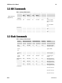
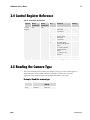
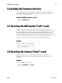
1
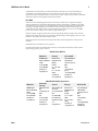
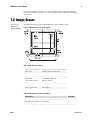
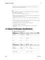
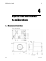
4M30 DS-44-04M30 DS-46-04M30 30 fps 2k x 2k CCD Camera User’s Manual and Reference Doc #: 03-32-10030 Rev: 03 4M30 Camera User’s Manual 2 © 2002 DALSA. All information provided in this manual is believed to be accurate and reliable. No responsibility is assumed by DALSA for its use. DALSA reserves the right to make changes to this information without notice. Reproduction of this manual in whole or in part, by any means, is prohibited without prior permission having been obtained from DALSA. About DALSA DALSA is an international high performance semiconductor and electronics company that designs, develops, manufactures, and markets digital imaging products and solutions, in addition to providing wafer foundry services. DALSA’s core competencies are in specialized integrated circuit and electronics technology, and highly engineered semiconductor wafer processing. Products include image sensor components; electronic digital cameras; and semiconductor wafer foundry services for use in MEMS, power semiconductors, image sensors and mixed signal CMOS chips. DALSA is a public company listed on the Toronto Stock Exchange under the symbol “DSA”. Based in Waterloo, On. Canada, the company has operations in Bromont, PQ; Colorado Springs, CO; Tucson, AZ; Eindhoven, NL; Munich, Germany and Tokyo, Japan. All DALSA products are manufactured using the latest state-of-the-art equipment to ensure product reliability. DALSTAR refers to all DALSA area scan products. For further information not included in this manual, or for information on DALSA’s extensive line of image sensing products, please contact us. DALSA Sales Offices Waterloo 605 McMurray Rd Waterloo, ON N2V 2E9 Canada Tel: 519 886 6000 Fax: 519 886 8023 www.dalsa.com [email protected] DALSA Waterloo Europe Asia Pacific 605 McMurray Rd Waterloo, ON N2V 2E9 Canada Tel: 519 886 6000 Fax: 519 886 8023 www.dalsa.com [email protected] Breslauer Str. 34 D-82194 Gröbenzell (Munich) Germany Tel: +49 - 8142 – 46770 Fax: +49 - 8142 – 467746 www.dalsa.com [email protected] Space G1 Building, 4F 2-40-2 Ikebukuro Toshima-ku, Tokyo 1710014 Japan +81 3 5960 6353 (phone) +81 3 5960 6354 (fax) www.dalsa.com [email protected] DALSA Worldwide Operations Colorado Tucson Europe Springs 5055 Corporate Plaza Drive Colorado Springs, CO 80919 USA Tel: 719 599 7700 Fax: 719 599 7775 www.dalsa.com [email protected] 3450 S. Broadmont Dr. Suite #128 Tucson, AZ 85713-5245 USA Tel: 520 791 7700 Fax: 520 791 7766 http://lifesciences.dalsa. com [email protected] Breslauer Str. 34 D-82194 Gröbenzell (Munich) Germany Tel: +49 - 8142 – 46770 Fax: +49 - 8142 – 467746 www.dalsa.com [email protected] Asia Pacific Space G1 Building, 4F 2-40-2 Ikebukuro Toshima-ku, Tokyo 1710014 Japan +81 3 5960 6353 (phone) +81 3 5960 6354 (fax) www.dalsa.com [email protected] 03-32-10030-03 4M30 Camera User’s Manual 3 &RQWHQWV Introduction to the 4M30 Camera ____________________________________________ 5 1.1 Camera Highlights ...................................................................................................................................................... 5 1.2 Image Sensor .............................................................................................................................................................. 6 1.3 Camera Performance Specifications............................................................................................................................ 7 Camera Hardware Interface ________________________________________________ 9 2.1 Installation Overview .................................................................................................................................................. 9 2.2 Input/Output ............................................................................................................................................................... 9 2.3 LED Status Indicators .................................................................................................................................................. 10 2.4 Power Input................................................................................................................................................................. 11 2.5 Data Output ................................................................................................................................................................ 12 2.6 Serial Communication................................................................................................................................................. 14 2.7 TTL Trigger Input and Output..................................................................................................................................... 16 2.8 Integration Time ......................................................................................................................................................... 18 2.9 Timing......................................................................................................................................................................... 18 Camera Operation ______________________________________________________ 20 3.1 How to Control the Camera......................................................................................................................................... 20 3.2 ADC Commands........................................................................................................................................................... 22 3.3 Clock Commands ......................................................................................................................................................... 22 3.4 Control Register Reference.......................................................................................................................................... 23 3.5 Reading the Camera Type........................................................................................................................................... 23 3.6 Reading the Firmware Revision.................................................................................................................................. 24 3.7 Resetting the ADC boards (“soft” reset)...................................................................................................................... 24 3.8 Resetting the Camera (“hard” reset) .......................................................................................................................... 24 3.9 Adjusting Gain ............................................................................................................................................................ 25 3.10 Adjusting User Offset ................................................................................................................................................ 26 3.11 Automatic Offset Control (AOC) ................................................................................................................................ 27 3.12 No Clean Mode.......................................................................................................................................................... 27 3.13 Triggering, Integration, and Frame Rate Overview ................................................................................................. 28 3.14 Controlling Integration (Shutter Time)..................................................................................................................... 28 3.15 Controlling Frame Rate............................................................................................................................................. 31 Optical and Mechanical Considerations ________________________________________ 34 4.1 Mechanical Interface ................................................................................................................................................... 34 DALSA 03-32-10030-03 4M30 Camera User’s Manual 4 4.2 Mechanical Tolerances ................................................................................................................................................ 35 4.3 Mounting the Camera ................................................................................................................................................. 35 Cleaning and Maintenance ________________________________________________ 36 5.1 Cleaning...................................................................................................................................................................... 36 5.2 Maintenance................................................................................................................................................................ 38 Troubleshooting ________________________________________________________ 39 Warranty _____________________________________________________________ 40 7.1 Limited One-Year Warranty........................................................................................................................................ 40 Appendix A ___________________________________________________________ 41 LVDS (EIA-644) Reference................................................................................................................................................ 41 Index _______________________________________________________________ 44 DALSA 03-32-10030-03 4M30 Camera User’s Manual 5 1 ,QWURGXFWLRQWRWKH0 &DPHUD 1.1 Camera Highlights Features • 2048 x 2048 resolution, full-frame CCD architecture • 30 fps four output, 4x40 MHz data rate • True 12-bit digitization • High sensitivity with low dark current • Progressive scan readout • Asynchronous image capture, externally triggerable to within 175 ns. • Programmable operation via RS232, including gain (1x – 10x), offset (±full scale), and triggering • 100% fill factor • DS-44-04M30 is the standard 4M30 camera • DS-46-04M30 has a sensor with taped on coverglass Description The 4M30 digital camera provides high-sensitivity 12-bit images with 2k x 2k spatial resolution at up to 30 frames per second (fps). The 4M30 is a full frame CCD camera using a progressive scan CCD to simultaneously achieve outstanding resolution and gray scale characteristics. A square pixel format and high fill factor provide superior, quantifiable image quality even at low light levels. Applications The 4M30 is an outstanding performer in fast, very high resolution applications. True 12 bit performance provides up to 4096 distinct gray levels—perfect for applications with DALSA 03-32-10030-03 4M30 Camera User’s Manual 6 large interscene light variations. The low-noise, digitized video signal also makes the camera an excellent choice where low contrast images must be captured in challenging applications. 1.2 Image Sensor This section is not applicable to part number DS-46-04M30 The 4M30 uses DALSA’s IA-DA-2048 high-performance full-frame CCD. Figure 1. IA-DA-2048 Image Sensor Block Diagram Table 1. IA-DA-2048 Sensor Structure Sensor characteristics Optical size 24.576mm (H) x 24.576 mm (V) Chip size 26.860 mm (H) x 26.508 mm (V) Pixel size 12µm x 12µm Active pixels 4 * [1024 (H) x 1024 (V)] Total number of pixels 2096 (H) x 2060 (V) Optical black pixels Left: 20 Right: 20 Timing pixels Left: 4 Right: 4 Dummy register cells Left: 7 Right: 7 Optical black lines Bottom: 6 Top: 6 Table 2. IA-DA-2048 Sensor Cosmetic Specifications DALSA Specification Grade 02 a) Number of first and last columns excluded 16 b) Number of first and last rows excluded 16 c) Maximum quantity of single pixel blemishes unspecified d) Maximum quantity of cluster blemishes 75 03-32-10030-03 4M30 Camera User’s Manual 7 Specification Grade 02 e) Maximum size of clusters (adjacent pixels) 30 f) Blemish pixel deviation from VFLL* under illumination >10% <45% g) Blemish pixel deviation from average dark level, measured at dark >20mV Notes: *VFLL is defined as the output signal under broadband quartz tungsten halogen light 2 with an irradiance of 4.08µW/cm . 1. All sensors are tested in four output mode – 1x gain. 2. Blemish variations are measured over an entire frame of data and counted within the frame boundaries defined by a) and b). 3. Blemishes are defined as a pixel or group of pixels with an output as defined in f) or g). 4. Clusters are defined as a pixel or group of pixel blemishes, and are allowed, provided they are smaller or equal to the sizes specified in e). 2 5. Illuminated blemish analysis done at 70% of VFLL (2.86µW/cm ). 6. Column and row defects not permitted. 7. Better than grade 02 sensors may be available. Please contact DALSA sales if interested. 1.3 Camera Performance Specifications Table 3: 4M30 Camera Performance Specifications Physical Characteristics Units Notes Resolution H x V pixels 2048x2048 Pixel Size µm 12x12 Pixel Fill Factor % 100 Size mm 146x92x14 3 Mass kg 1.3 Power Dissipation W < 24 Lens Mount Aperture mm 24.6 x 24.6 Operating Ranges Units Min. Frame Rate Fps Data Rate MHz Data Format LVDS Responsivity DALSA F mount Max. 30 4*40 4*40 4*12 bit 2 DN/(nJ/cm ) 24@530nm 4 Operating Temp °C 10 40 +15 Input Voltage V +14.925 +15.075 +5 Input Voltage V +4.975 +5.025 03-32-10030-03 4M30 Camera User’s Manual 8 Physical Characteristics Units -5 Input Voltage V Notes Nominal Gain Range - 4.975 - 5.025 1x 10x Calibration Conditions Units Setting Min. Max. Data Rate MHz 4x40 4x40 4x40 +15 Input Voltage V +15 +14.925 +15.075 +5 Input Voltage V +5 +4.975 +5.025 -5 Input Voltage V - 5 - 4.975 - 5.025 Ambient Temperature °C 25 Gain X 1x Electro-Optical Specifications Units Min. Typical Max. Dynamic Range dB 64.0 67.0 Pixel Response NonUniformity %rms 2.0 3.0 System Noise DN(rms) 2.1 2.4 1 2, 4 Notes: 1. Dynamic Range = 20 * log10[(Counts @ Full Well)/Read Noise] 2. PRNU = [[[STDEV(100 frames @ saturation)/(MEAN @ saturation)]-Dark Offset(in darkness)]*100 - - 3. System Noise = Read Noise (e )/Gain (e /DN) dark measurement 4. Specification not applicable to the DS-45-04M30 due to Lumogen coated sensor DALSA 03-32-10030-03 4M30 Camera User’s Manual 9 2 &DPHUD+DUGZDUH ,QWHUIDFH 2.1 Installation Overview In order to set up your camera, you should take these initial steps: This installation overview assumes you have not installed any system components yet. 1. Power down all equipment. 2. Following the manufacturer’s instructions, install the frame grabber (if applicable). Be sure to observe all static precautions. 3. Install any necessary imaging software. 4. Before connecting power to the camera, test all power supplies. Ensure that all the correct voltages are present at the camera end of the power cable (Refer to the Camera Performance Specifications on page 7). Power supplies must meet the requirements defined in section 2.4 Power Input. 5. Inspect all cables and connectors prior to installation. Do not use damaged cables or connectors or the camera may be damaged. 6. Connect data, serial interface, and power cables. 7. After connecting cables, apply power to the camera. The POST (power on self test) LED on the back of the camera should glow green after one second to indicate that the camera is operating and ready to receive commands. 2.2 Input/Output The camera provides 12-bit LVDS data and synchronization signals through the data output connector. Camera functions such as integration time, camera gain and offset are all controllable by the user via the RS232 serial port. The camera is capable of free running operation or may be triggered externally via the input TRIGGER IN. TRIGGER OUT allows the synchronization of shutters or illumination sources in free running or externally triggered modes. DALSA 03-32-10030-03 4M30 Camera User’s Manual 10 Figure 2: Camera Inputs/Outputs &KDQQHOGDWDRXWSXW &KDQQHOGDWDRXWSXW /('6WDWXVLQGLFDWRUV /('6WDWXVLQGLFDWRUV &KDQQHOGDWDRXWSXW &KDQQHOGDWDRXWSXW &KDQQHOGDWDRXWSXW &KDQQHOGDWDRXWSXW 7ULJJHULQSXWRXWSXW 3RZHUVXSSO\LQSXW 3RZHUVXSSO\LQSXW 6HULDOSRUW 2.3 LED Status Indicators There are four LED's visible on the rear cover of the camera that indicate the camera’s status. Table 4: LED Functions DALSA LED Label Color LED “ON” LED “OFF” ON Green Camera is receiving power No camera power POST Green Camera Power On Self Test successful Camera failed Power On Self Test BIN Green Not Operational Not Operational MODE Green Camera is in an external trigger mode (uses external signal to trigger image capture) Camera is triggering image capture internally 03-32-10030-03 4M30 Camera User’s Manual 11 2.4 Power Input Table 5: Power Connector Pinout ! WARNING: It is extremely important that you apply the appropriate voltages to your camera. Incorrect voltages will damage the camera. Pin Symbol 1 +5V 9 1 The camera has the following input power requirements: 2 +5V V 3 - 5V (DC) 4 +15V 5 NC 6 NC 7 GND 8 GND 9 +5V 10 - 5V 11 +15V 12 +15V 13 NC 14 GND 15 GND 15 8 DB15M (AMP Part # 747236-4 or equivalent) r% Max Ripple mV A +15 .0.5 < 50 0.5 +5 0.5 < 50 3.7 -5 0.5 < 50 0.8 Note: Performance specifications are not guaranteed if your power supply does not meet these requirements. DALSA offers a linear power supply (with cables) that meets the 4M30’s requirements (Universal Power Supply, part number 24-00001-02, contact DALSA for more information), but it should not be considered the only choice. Many high quality supplies are available from other vendors. DALSA assumes no responsibility for the use of these supplies. When setting up the camera’s power supplies, follow these guidelines: x Do not connect or disconnect cable while power is on. x Do not use the shield on a multi-conductor cable for ground. x Keep leads as short as possible to reduce voltage drop. x Use high-quality linear supplies to minimize noise. DALSA 03-32-10030-03 4M30 Camera User’s Manual 12 2.5 Data Output Figure 3 illustrates the data channel outputs when viewed from the front of the CCD. Arrows indicate channel read out direction. Figure 3: Channel read out direction The camera back panel output connectors DATA1, DATA 2, DATA 3, and DATA 4 utilize differential LVDS signals with pin assignments described in Table 6. Connector and Pinout Table 6: DATA Connector Pinout Pin Symbol Pin Symbol Pin Symbol Pin Symbol 1 D*0+ 16 Reserved 31 NC 46 GND 2 D*0- 17 D*7+ 32 NC 47 NC 3 D*1+ 18 D*7- 33 NC 48 NC 4 D*1- 19 D*8+ 34 NC 49 NC 5 D*2+ 20 D*8- 35 NC 50 NC 6 D*2- 21 D*9+ 36 NC 51 NC 7 D*3+ 22 D*9- 37 NC 52 NC 8 D*3- 23 D*10+ 38 NC 53 Reserved 9 D*4+ 24 D*10- 39 NC 54 Reserved 10 D*4- 25 D*11+ 40 NC 55 VSYNC- 11 D*5+ 26 D*11- 41 NC 56 VSYNC+ 12 D*5- 27 NC 42 NC 57 HSYNC- 13 D*6+ 28 NC 43 NC 58 HSYNC+ 14 D*6- 29 NC 44 NC 59 PIXCLK- 15 Reserved 30 NC 45 GND 60 PIXCLK+ 16 15 46 45 60 31 30 1 (Molex Part # 70928-2000 or equivalent) NC = No Connect. These pins are unused. DALSA 03-32-10030-03 4M30 Camera User’s Manual ! 13 WARNING. Care must be taken when connecting data cables to the camera to insure proper connection and to prevent damage to the connector. Data Signals Table 7: Data Signal Definition IMPORTANT: This camera uses the TOZZW\Uedge of the pixel clock to register data. Signal Description D*0+, D*0- Data bit 0 true and complement—Output. (Least significant bit.) D*1+, D*1- Data bit 1 true and complement—Output. D*2+, D*2- Data bit 2 true and complement—Output. D*3-D*10+,- etc. Etc. D*11+, D*11- Data bit 11 true and complement—Output. (Most significant bit.) Digitized video data is output from the camera as LVDS differential signals using 4 Molex 60-pin connectors on the rear panel (labeled “DATA 1 through DATA 4”). The data is synchronous and is accompanied by a pixel clock and clocking signals. Data Clocking Signals Table 8: Clock Signal Descriptions Signal Description PIXCLK+, PIXCLK- Pixel clock true and complement. 40MHz—Output. Data is valid on the falling edge. HSYNC+, HSYNC- Horizontal sync, true and complement—Output. HSYNC high indicates the camera is outputting a valid line of data. VSYNC+, VSYNC- Vertical sync, true and complement—Output. VSYNC high indicates the camera is outputting a valid frame of data. 2.6 Serial Communication Connector and Pinout The serial interface provides control of frame rate, integration time (shuttering), video gain and offset, external trigger and external integration. For information on how to control these functions, see Camera Operation, beginning on page 20. The remote interface consists of a two-wire (plus ground) full duplex RS-232 compatible serial link, used for camera configuration, and two back panel SMA coax connectors used for external trigger input and output. DALSA 03-32-10030-03 4M30 Camera User’s Manual The camera uses an RJ-11 telephone-style connector for serial communications, with four conductors installed in a sixposition connector. Note that both four- and six- conductor plugs may be used interchangeably with the RJ-11 jack. IMPORTANT: Both the PC/AT and the camera are configured as “DTE” (Data Terminal Equipment) devices requiring the TXD and RXD lines to be swapped when interconnecting the two (note that pin 4, normally the yellow wire, is not used on the RJ-11.) That is, the TXD pin represents DATA OUT and the RXD pin represents DATA IN on both devices, so that one device’s TXD line must connect to the other device’s RXD line and vice-versa. 14 GND TXD RXD RJ-11 View into female jack 6-position with 4 conductors Figure 4: 25 Pin Serial Port Connector to Camera RJ-11 Connector Figure 5: 9 Pin Serial Port Connector to Camera RJ-11 Connector DALSA 03-32-10030-03 4M30 Camera User’s Manual 15 Serial Communication Settings Table 9: Serial Port Configuration Serial Port Configuration Baud 9600, fixed Start bits 1 Data bits 8 Stop bits 1 Parity None The serial interface operates at RS-232 levels with fixed parameters of 9600 baud, 1 start bit, 8 data bits, 1 stop bit, and no parity. The interface uses only three wires, for received data, transmitted data, and ground. In general writing data must start with a write command byte and be followed by a data byte. Reading a camera register requires only a single read command byte. ! WARNING: Due to initialization sequencing after power-up, no commands should be sent to the camera for a minimum of 1 second after power up. The remote interface connector, on the cameras rear panel, is specified as a lowprofile RJ-11 modular connector. The connector is a 6-position model, but only the center four positions are populated with contacts. It will mate with either the 4position or 6-position cable plugs. This type of connector typically requires special assembly tools; complete cable assemblies are available from suppliers such as Digi-Key: Serial Cable Source Digi-Key 701 Brooks Ave. South Thief River Falls, MN 56701 1-800-344-4539 cable part number: H2643-14-ND (14 feet) DALSA provides serial cables in 3 lengths: 10’, 20’ and 50’. Part number CL-31-00004xx (where xx refers to the cable length in feet). 2.7 TTL Trigger Input and Output Connector The camera uses an SMA connector (labeled TRIGGER IN) to allow the user to provide a standard TTL signal to control camera integration and readout. The input is high impedance (>10.5K), allowing the user to terminate at the SMA input as needed. The camera has another SMA connector (TRIGGER OUT) that provides a standard TTL output which is high whenever the camera is integrating. DALSA 03-32-10030-03 4M30 Camera User’s Manual 16 Figure 6: Trigger Timing Description 2.8 Integration Time The minimum integration time (or shutter time) is 10 Ps. As with any full frame imager, the camera will continue to integrate during read out unless externally shuttered or strobed. 2.9 Timing The 4M30 pixel clock runs at 40 MHz, so each pixel clock cycle will be 1/40,000,000 or 25ns. The following diagram and tables describe the correct timing requirements for the 4M30 camera. Figure 7: 4M30 Timing VSYN C H SYN C A D a ta B C 1 2 3 D E F C P IX E L CLOCK DALSA 03-32-10030-03 4M30 Camera User’s Manual 17 “A” represents the number of falling clock edges from the rising edge of VSYNC to the rising edge of HSYNC. “B” represents the number of falling clock edges prior to the first word. (Pre-Scan pixels) “C” represents the number of words per line. “D” represents the number of falling clock edges between the last word and the falling edge of HSYNC. (Post-Scan pixels) “E” represents the number of falling clock edges between a falling HSYNC and a rising HSYNC. “F” represents the number of falling clock edges from the falling edge of HSYNC to the falling edge of VSYNC Table 10: HSYNC Pixel Timing IMPORTANT: This camera uses the TOZZW\Uedge of the pixel clock to register data. DALSA Horizontal Binning Mode A B C D E F 1x 213 18 1024 18 196 2 Table 11: VSYNC Pixel Timing (HSYNC falling edges/VSYNC falling edge) Vertical Binning Mode Pre-Scan Lines/Frame Active Lines/Frame Post Scan Lines/Frame 1x 6 1024 0 03-32-10030-03 4M30 Camera User’s Manual 18 3 &DPHUD2SHUDWLRQ 3.1 How to Control the Camera The 4M30’s RS-232-compatible serial interface allows you to control its configuration and operation, including: • Triggering Mode • Frame Rate • Integration Time • Gain • Offset • Reset Command Protocol Overview The camera accepts 8-bit command/value pairs via its RJ-11 serial port using RS-232 compatible signals. Camera commands are divided into two basic sets: DALSA Serial Port Configuration Baud 9600, fixed Start bits 1 Data bits 8 Stop bits 1 • “clock” commands which apply to the Parity None electronics that drive the image sensor. These include clock generation, frame rate, integration time, and binning. Clock commands effect the entire camera, and are not channel specific. A single command will impact all channels. • “ADC” commands which apply to the electronics that process and digitize the video. These include gain and offset. ADC commands are channel specific. Four separate commands must be issued to change all four channels. 03-32-10030-03 4M30 Camera User’s Manual • 19 Each set of commands includes read and write variants. With the exception of reset commands, all 8-bit write commands must be followed by an 8-bit data byte. The commands are interpreted as follows: Table 12: ADC Bit Definitions ! Bit Function 0:3 Command Register Address (Reference Table 12) 4:5 ADC Board Address 00 = ADC Channel 1 01 = ADC Channel 2 10 = ADC Channel 3 11 = ADC Channel 4 6 Command Type 0 = Write 1 = Read 7 Board Type 0 = ADC Board 1 = Clock Board • Any commands not listed in this manual should be considered invalid to the 4M30 user. • A number of functions and modes depend on the ADC/Control Register settings. These settings are detailed in the following sections. • The “Write Control Register” command is used to write data that controls specific camera triggering and test functions. This command must be followed by a data byte with bits defined in Table 15. • The “Read” command allows interrogation of the camera to determine current configuration. WARNING: Any commands not listed should be considered invalid. Writing to invalid addresses may overwrite camera calibration information, requiring the camera to be returned for recalibration. WARNING: Due to initialization sequencing after power-up, no commands should be sent to the camera for a minimum of 1 second after power up. DALSA 03-32-10030-03 4M30 Camera User’s Manual 20 3.2 ADC Commands Table 13: Summary of ADC Commands Control * Reference Table 11 for appropriate entry Write Command Read Command Hex Binary Hex Binary ADC Board Soft Reset *0h 00** 0000 NA User Offset *2h 00** 0010 *3h User Gain AOC Channel Function NA 1,2,3,4 Resets ADC board only *2h 01** 0010 1,2,3,4 LS byte of 16 bit user controllable offset 00** 0011 *3h 01** 0011 1,2,3,4 MS byte of 16 bit user controllable offset *5h 00** 0101 *5h 01** 0101 1,2,3,4 LS byte of 16 bit gain *6h 00** 0110 *6h 01** 0110 1,2,3,4 MS byte of 16 bit gain *8h 00** 1000 NA NA 1,2,3,4 AOC Adjustment Channel Function 3.3 Clock Commands Table 14: Summary of Clock Commands Control Write Command Read Command Hex Binary Hex Binary Reset Camera 80h 1000 0000 NA NA 1,2,3,4 Resets all registers to default values Read Camera Type NA NA C3h 1100 0011 1,2,3,4 Returns Camera ID register (4Bh) Read Firmware Rev NA NA C5h 1100 0101 1,2,3,4 Returns Firmware revision register Control Register 82h 1000 0010 C2h 1100 0010 1,2,3,4 Control Register settings Integration Time 8Ah 1000 1010 NA NA NA Write byte 0 of 18 bit integration time 8Bh 1000 1011 NA NA NA Write byte 1 of 18 bit integration time 8Ch 1000 1100 NA NA NA Write byte 2 of 18 bit integration time 8Dh 1000 1101 NA NA NA Write byte 0 of 18 bit frame rate time 8Eh 1000 1110 NA NA NA Write byte 1 of 18 bit frame rate time 8Fh 1000 1111 NA NA NA Write byte 2 of 18 bit frame rate time Frame Rate DALSA 03-32-10030-03 4M30 Camera User’s Manual 21 3.4 Control Register Reference Table 15: Control Register Bit Definitions Register Write Command Read Command Bit Function Default Control Register 82h C2h 7 Integration Mode 0=Internal 1=External 1 6:4 Always 0 000 3 Trigger Mode 0=Internal 1=External 0 2 No Clean Mode (External Integration Only) 0 = Camera flushes charge between frames 1 = Charge is not flushed 1 1 Always 0 0 0 Serial Trigger Bit 0 3.5 Reading the Camera Type This read command returns an 8-bit value unique to the type of camera interrogated. A 4M30 will return a value of 4Bh when this command is issued. This is useful for applications that need to function with multiple DALSTAR camera types. Example: Read the camera type DALSA Command Value Returned (4M30) Binary 1100 0011 0100 1011 Hex C3h 4Bh 03-32-10030-03 4M30 Camera User’s Manual 22 3.6 Reading the Firmware Revision This command returns a byte in which the lower nibble is the revision number for the clock board firmware and the upper nibble is undefined. The ability to read this value may assist in customer support issues. Example: Read the firmware version Command Binary 1100 0101 Hex C5h 3.7 Resetting the ADC boards (“soft” reset) When this command is issued, the microprocessor on the ADC board will restart execution as if the micro was just powered up. This causes the dark reference control loop to restart at its initial values before settling in to the calibrated dark reference level of approximately 50 counts. This is useful because under some conditions, issuing a soft reset to the ADC board’s microprocessor after camera operating conditions have changed will improve the rate at which the offset control loop pulls into the calibrated level. This is one of only two “write” commands that are not followed by a data byte. Example Use this command to reset ADC Channel 3: Command Value Binary 0010 0000 - Hex 20h - 3.8 Resetting the Camera (“hard” reset) This is the only other “write” command that is not followed by a data byte. This command resets all clock board registers to their default values (the values used at power-up). Example Use this command to reset the camera: DALSA Command Value Binary 1000 0000 - Hex 80h - 03-32-10030-03 4M30 Camera User’s Manual 23 Table 16: Default values in effect after reset Feature 4M30 Default Frame Rate (fps) External Cntrl Integration Time (ms) External Cntrl Video Gain 1x Pixel Offset 50 DN Trigger Mode External Integration Control External Data Rate (MHz) 4x40 3.9 Adjusting Gain Video gain is adjustable from 1.0 to 10.0 by writing a 16 bit value as an MS and LS byte (only the 14 most significant bits of this value are actually used). The amplifier used for gain control has a ranger of 40 dB, which equates to an adjustment increment of 0.00244 14 dB (40dB/2 ). The camera gain value is calculated according to the following equation: Value # 27306*log10(Gain) Where 1.0 d Gain d 10.0 Example: Set Channel 1 to 2.5x Gain Use these command/value pairs set the camera to 2.5x gain (you must write both MSB and LSB values to all four ADC channels). Value # 27306 u log10(2.5) Value = 10866 = 2A72h Write MSB Command DALSA Write LSB Value Command Value Binary 0000 0110 0010 1010 0000 0101 0111 0010 Hex 06h 2Ah 05h 72h 03-32-10030-03 4M30 Camera User’s Manual 24 Reading Channel 3 Gain from the Camera To read the gain setting from the camera, use these commands: Read MSB Read LSB Binary 0110 0110 0110 0101 Hex 66h 65h 3.10 Adjusting User Offset User offset is adjustable from minus full scale to plus full scale (±4095) by a 16 bit value as an MS and LS byte (only the 14 most significant bits of this value are actually used). There are 4 ADC video boards in the 4M30 and each can be controlled independently. Normally, the same value will be written to all four channels. The value is calculated according to the following equation: Value # 218 u Offset/Gain Where Offset is in counts and –4095 d Offset d 4095 And 1 d Gain d 10 and is defined as above. This means that the offset is dependent on the gain and can be adjusted with a resolution of 0.5 x Gain (in DN counts). Example: Set Channel 2 to 20 DN Offset @ 2.5x Gain Use these command/value pairs set the camera to an offset of 20 DN at a gain of 2.5 (you must write both MSB and LSB values). Value # 218 u 20/2.5 Value = 1744 = 06D0h Write MSB Binary Hex DALSA Write LSB Command Value Command Value 0001 0011 0000 0110 0001 0010 1101 0000 06h 12h D0h 13h 03-32-10030-03 4M30 Camera User’s Manual 25 The read user offset commands allow the user to read back this information from the camera. Reading Channel 4 Offset from the Camera To read Channel 4 offset setting from the camera, use these commands: Read MSB Read LSB Binary 0111 0011 0111 0010 Hex 73h 72h 3.11 Automatic Offset Control (AOC) The AOC defines the digitized value of black for the camera. An ideal camera (no dark current, no shot noise, etc.) in total darkness produces an image with all pixels equal to the AOC set point value. This command allows you to control the AOC set point of the ADC video board. The four ADC video boards in the 4M30 can each be controlled independently. Normally all channels are controlled with the same set point value. The default value is 50 DNs, or counts. Example: Set the Channel 2 AOC Set Point to 32 DNs Value = 32 = 20h Command Value Binary 0001 1000 0010 0000 Hex 18h 20 3.12 No Clean Mode There is no way to prevent the CCD imager from integrating (accumulating charge due to light falling on the imager). Under some conditions this will cause the image to show smearing in the vertical direction, and increase Dark Current. In order to reduce this effect, the 4M30 camera runs horizontal and vertical clocks during idle time to flush the charge. Under some conditions, this feature may be undesirable. For example, when wanting to synchronize camera integration to an external event in the External Integration Mode. Under these conditions, the user can enable the No Clean Mode by setting bit [2] in the Control Register = 1. No Clean Mode can only be enabled when in Programmed Integration Mode (bit [7] of the Control Register =1) DALSA 03-32-10030-03 4M30 Camera User’s Manual 26 Example: Enable No Clean Mode Command Value Binary 1000 0010 1*** *1** Hex 82h **h Note: The register containing the No Clean bit also controls other configuration data (*). All bits must be set appropriately. 3.13 Triggering, Integration, and Frame Rate Overview Image capture triggering, integration, and frame rate are closely related. • Integration time can be less than 1/frame rate, but it can never be greater than 1/frame rate. • You can program fixed integration (or use default) and let the camera “free run.” • You can program fixed integration time and supply a (asynchronous) trigger signal to control frame rate by supplying a TTL pulse on the SMA connector. This is referred to as “Programmed Integration/External Trigger Mode.” • You can also have the camera integrate as long as an asynchronous TTL pulse is held high. This pulse will therefore control both integration time and frame rate. This is also known as “External Integrate Mode.” For a given frame rate, the maximum integration time is limited to the frame period less an overhead factor required for proper operation of the CCD. Maximum integration time is defined by this equation: Max Integration Time = (1/Frame Rate) – 32.35 ms This equation is valid for all modes, free running, external trigger and external integrate modes. ! WARNING: Do not set integration time higher than the limits of the equation above. Unpredictable operation may result 3.14 Controlling Integration (Shutter Time) The 4M30 allows you to control integration (also known as exposure time or shutter time) in these ways. DALSA • Programmed Integration/Free Running: (default) The camera free runs with the internally programmed integration time and frame rate • Programmed Integration/SMA Trigger: The camera will integrate for the internally programmed time when triggered by a high going TTL pulse on the SMA connector. • Programmed Integration/Serial trigger: The camera will integrate for the internally programmed time when triggered by a high going Serial Trigger signal. • External Integration/SMA Trigger: The camera will integrate as long as the TTL pulse on the TRIGGER IN SMA connector is high. The integration time is effectively the input pulse width. In this mode, TRIGGER IN also controls the frame rate. 03-32-10030-03 4M30 Camera User’s Manual • 27 External Integration/Serial Trigger: The camera will integrate as long as the Serial Trigger signal is held high. The integration time is effectively the input pulse width. In this mode, the serial signal also controls the frame rate. Due to variation in the host operating system, this mode is generally used only for camera setup and functional testing. The register settings required for each mode are defined in Table 17: Integration/Trigger Modes. Table 17: Integration/Trigger Modes Mode Control Register Bit [7] INTEGRATE Control Register Bit [3] EXT Trigger Programmed Integration/Free Running 0 0 Programmed Integration/SMA Trigger 0 1 Programmed Integration/Serial Trigger 0 1 External Integration/SMA Trigger 1 1 External Integration/Serial Trigger 1 1 Whenever the Integrate Mode or External Trigger Mode bits are set the MODE LED on the right side of the rear cover will light to indicate that an externally synchronized mode is active. Free Running (Programmed Integration): The camera speed is controlled by writing a 3-byte integration time value (in µs) to the three Integration Time registers. These three bytes are then combined to form a 24 bit integration time. The number represents the integer number of microseconds the camera will collect light. The number programmed in the three registers should not be below 10 PS (0000Ah). The camera will run at maximum speed for the programmed integration time. Example: Set integration time to 10ms With an internal integration time of 10 ms, the camera will operate at 23.6 fps. 1/Frame Rate = 10 ms + 32.35 ms = 42.35 ms 1. Using the command 82h, set bit [7] of the data byte to 0 (Integration Mode = Internal) and bit [3] of the data byte to 0 (Trigger Mode = Internal). NOTE: All bits within the register are written at one time. Ensure the correct value for all bits are used when changing camera modes. 2. Use commands 8Ah, 8Bh, 8Ch to set the 24-bit integration time value. Value = 10 ms = 10000 µs = 002710h DALSA 03-32-10030-03 4M30 Camera User’s Manual 28 Write Integration LS Byte Write Integration Center Byte Write Integration MS Byte Command Value Command Value Command Value Binary 1000 1010 0001 0000 1000 1011 0010 0111 1000 1100 0000 0000 Hex 8Ah 10h 8Bh 27h 8Ch 00h Programmed Integration/SMA Trigger For external SMA controlled triggering with a programmed integration time, a TTL rising edge on TRIGGER IN connector triggers the camera to acquire one frame of data. Integration begins within 175 ns after the rising edge and stops when the programmed integration time has completed. After that single frame acquisition, the camera outputs the just acquired frame and “re-arms”, thus waiting for a new External Trigger signal to trigger a new frame acquisition. The camera is “armed” when the read out of the acquired frame is completed. No additional rising edges, or triggers, should be allowed during the image acquisition or frame read out. When the camera is in External Trigger Mode, the MODE LED will be illuminated on the camera back to indicate the camera is expecting a signal on the TRIGGER IN connector or Serial Trigger bit [0] of the Control Register. Because this signal is internally OR’ed with the Serial Trigger bit [0] of the Control Register, care must be taken to ensure the bit [0] of the Control Register is not changed from logic 0 to 1 while triggering with the TRIGGER IN connector. Programmed Integration/Serial Trigger For external serial controlled triggering with a programmed integration time, a TTL rising edge on bit [0] of the Control Register triggers the camera to acquire one frame of data. Integration begins within 175 ns after the rising edge and stops when the programmed integration time has completed. After that single frame acquisition, the camera outputs the just acquired frame and “re-arms”, thus waiting for a new External Trigger signal to trigger a new frame acquisition. The camera is “armed” when the read out of the acquired frame is completed. No additional rising edges, or triggers, should be allowed during the image acquisition or frame read out. When the camera is in External Trigger Mode, the MODE LED will be illuminated on the camera back to indicate the camera is expecting a signal on serial bit [0] of the Control Register, or the TRIGGER IN connector. Because this signal is internally OR’ed with the TRIGGER IN input, care must be taken to ensure the TRIGGER IN signal is not changed from logic 0 to 1 while triggering with bit [0] of the Control Register. External Integration/SMA Trigger When in External Integration/SMA mode, a TTL rising edge on the TRIGGER IN signal triggers the camera to acquire one frame of data. Integration begins within 175 ns after the rising edge and stops within 200 ns after the falling edge. After that single frame acquisition, the camera outputs the just acquired frame and “re-arms”, thus waiting for a DALSA 03-32-10030-03 4M30 Camera User’s Manual 29 new External Trigger signal to trigger a new frame acquisition. The camera is “armed” when the read out of the acquired frame is completed. No additional rising edges, or triggers, should be allowed during the image acquisition or frame read out. This means in this mode TRIGGER IN necessarily controls both integration and frame rate. When the camera is in External Integration Mode, the MODE LED will be illuminated on the camera back to indicate the camera is expecting a signal on the TRIGGER IN connector or Serial Trigger bit [0] of the Control Register. Because this signal is internally OR’ed with the Serial Trigger bit [0] of the Control Register, care must be taken to ensure the bit [0] of the Control Register is not changed from logic 0 to 1 while triggering with the TRIGGER IN connector. External Integration/Serial Trigger When in External Integration/Serial mode, a TTL rising edge on bit [0] of the Control Register triggers the camera to acquire one frame of data. Due to variation in the host operating system, this mode is generally used only for camera setup and functional testing. Integration begins within 175 ns after the rising edge and stops within 200 ns after the falling edge. After that single frame acquisition, the camera outputs the just acquired frame and “re-arms”, thus waiting for a new External Trigger signal to trigger a new frame acquisition. The camera is “armed” when the read out of the acquired frame is completed. No additional rising edges, or triggers, should be allowed during the image acquisition or frame read out. This means in this mode TRIGGER IN necessarily controls both integration and frame rate. When the camera is in External Integration Mode, the MODE LED will be illuminated on the camera back to indicate the camera is expecting a signal on serial bit [0] of the Control Register, or the TRIGGER IN connector. Because this signal is internally OR’ed with the TRIGGER IN input, care must be taken to ensure the TRIGGER IN signal is not changed from logic 0 to 1 while triggering with bit [0] of the Control Register. 3.15 Controlling Frame Rate The 4M30 allows you to control frame rate in three ways: DALSA • Free Running (Programmed Integration time): The camera free runs with the internally programmed integration time which can be used to set frame rate. • External Trigger/Internal Integration: The camera frame rate will be controlled by the TTL pulse on the TRIGGER IN SMA connector or serial bit [0] of the Control Register. The camera will integrate for the programmed integration time. For more information, refer to section 3.14 Controlling Integration Mode. • External Integration: The camera frame rate will be controlled by the TTL pulse on the TRIGGER IN SMA connector or serial bit [0] of the Control Register. The camera will integrate for as long as the pulse is held high. In this mode, TRIGGER IN also controls integration. For more information, refer to section 3.14 Controlling Integration Mode. 03-32-10030-03 4M30 Camera User’s Manual 30 Free Running Frame Rate can only be controlled by setting integration time. To specify programmed frame rate (by using integration time): 1. Set bit [7] of the Control Register to 0 (Integrate Mode = Internal), and bit [3] of the Control Register to 0 (Trigger Mode = Internal). To determine the integration time needed for a specific frame rate use the following equation: Integration Time = (1/Frame rate) - 32.35ms 2. Write the 3-byte Integration value (in µs) to the three Integration registers. These three bytes are then combined to form a 24 bit frame Integration time. The number programmed in the three registers should not be below 10 PS (0000Ah), or above the calculated value noted in section 3.13 Triggering, Integration, and Frame Rate Overview. 3. Using the command 82h, set bit [7] of the data byte to 0 (Integration Mode = Internal) and bit [3] of the data byte to 0 (Trigger Mode = Internal). NOTE: All bits within the register are written at one time. Ensure the correct value for all bits are used when changing camera modes. 4. Use commands 8Ah, 8Bh, 8Ch to set the 24-bit Integration time value. Value = 1/25s –32.35ms = 4650 µs = 00122Ah Write Frame Rate LS Byte Write Frame Rate Center Byte Write Frame Rate MS Byte Command Value Command Value Command Value Binary 1000 1010 0010 1010 1000 1011 0001 0010 1000 1100 0000 0000 Hex 8Ah 2Ah 8Bh 12h 8Ch 00h External Trigger/Programmed Integration This is the same as Programmed Integration/SMA Trigger Mode or Programmed Integration/Serial Trigger Mode. Reference to section 3.14 Controlling Integration Mode. Example: Set the Frame Rate to 2.5 fps 1. Refer to section 3.13 Triggering, Integration, and Frame Rate Overview to ensure that the desired frame rate can be supported for the selected binning and integration modes. 2. Using the command 81h, set bit [0] of the data byte to 0 (Integration Mode = Internal) and bit [3] of the data byte to 1 (Trigger Mode = External). NOTE: All bits within the register are written at one time. Ensure the correct value for all bits are used when changing camera modes. 3. DALSA Set the desired integration time per section 3.14 – Controlling Integration. 03-32-10030-03 4M30 Camera User’s Manual 4. 31 Each TTL rising edge on the SMA connector or serial bit [0] of the Control Register will initiate a new frame of data, using the programmed integration time. To achieve 2.5 fps, a TTL pulse must be sent to the camera every 400 ms (1/2.5). External Integration This is the same as the External Integration/SMA Trigger Mode or the External Integration/Serial Trigger Mode. Refer to section 3.14 Controlling Integration Mode. DALSA 03-32-10030-03 4M30 Camera User’s Manual 32 4 2SWLFDODQG0HFKDQLFDO &RQVLGHUDWLRQV 4.1 Mechanical Interface Figure 8: Camera Dimensions DALSA 03-32-10030-03 4M30 Camera User’s Manual 33 4.2 Mechanical Tolerances Not applicable to part number DS-46-04M30 Table 18: Mechanical Tolerances Additional Dimensions Center of sensor with respect to lens mount ´ Planarity of lens flange to sensor " Rotation of sensor ° 4.3 Mounting the Camera The 4M30 can be mounted via the 3/8” deep, 1/4”-20 threaded tripod mount located on the bottom of the camera. DALSA 03-32-10030-03 4M30 Camera User’s Manual 34 5 &OHDQLQJDQG 0DLQWHQDQFH 5.1 Cleaning This section is not applicable to part number DS-46-04M30 Electrostatic Discharge and the CCD Sensor Charge-coupled device (CCD) image sensors are metal oxide semiconductor (MOS) devices and are susceptible to damage from electrostatic discharge (ESD). Although many sensor pins have ESD protection circuitry, the ESD protection circuitry in CCDs is typically not as effective as those found in standard CMOS circuits. Electrostatic charge introduced to the sensor window surface can induce charge buildup on the underside of the window that cannot be readily dissipated by the dry nitrogen gas in the sensor package cavity. When charge buildup occurs, surface gated photodiodes (SGPDs) may exhibit higher image lag. Some SGPD sensors may also exhibit a highly non-uniform response when affected by charge build-up, with some pixels displaying a much higher response when the sensor is exposed to uniform illumination. The charge normally dissipates within 24 hours and the sensor returns to normal operation. Preventing ESD Damage To prevent ESD damage, DALSA advises you to take the following handling precautions. 1. Ground yourself prior to handling CCDs. 2. Ensure that your ground and your workbench are also properly grounded. Install conductive mats if your ground or workbench is non-conductive. 3. Use bare hands or non-chargeable cotton gloves to handle CCDs. NOTE: Rubber fingercots can introduce electrostatic charge if the rubber comes in contact with the sensor window. 4. Handle the CCD from the edge of the ceramic package and avoid touching the sensor pins. 5. Do not touch the window, especially in the region over the imaging area. DALSA 03-32-10030-03 4M30 Camera User’s Manual 35 6. Ground all tools and mechanical components that come in contact with the CCD. 7. DALSA recommends that CCDs be handled under ionized air to prevent static charge buildup. 8. Always store the devises in conductive foam. Alternatively, clamps can be used to short all the CCD pins together before storing. The above ESD precautions need to be followed at all times, even when there is no evidence of CCD damage. The rate which electrostatic charge dissipates depends on numerous environmental conditions and an improper handling procedure that does not appear to be damaging the CCDs immediately may cause damage with a change in environmental conditions. Protecting Against Dust, Oil, and Scratches The CCD window is part of the optical path and should be handled like other optical components, with extreme care. Dust can obscure pixels, producing dark patches on the sensor response. Dust is most visible when the illumination is collimated. The dark patches shift position as the angle of illumination changes. Dust is normally not visible when the sensor is positioned at the exit port of an integrating sphere, where the illumination is diffuse. Dust can normally be removed by blowing the window surface using clean, dry, compressed air, unless the dust particles are being held by an electrostatic charge, in which case either an ionized blower or wet cleaning is necessary. Oil is usually introduced during handling. Touching the surface of the window barehanded will leave oily residues. Using rubber fingercots and rubber gloves can prevent contamination. However, the friction between rubber and the window may produce electrostatic charge that may damage the sensor. To avoid ESD damage and to avoid introducing oily residues, only hold the sensor from the edges of the ceramic package and avoid touching the sensor pins and the window. Improper handling, cleaning or storage of the sensor can cause scratches. Vacuum picking tools should not come in contact with the window surface. CCDs should not be stored in containers where they are not properly secured and can slide against the container. Scratches diffract incident illumination. When exposed to uniform illumination, a sensor with a scratched window will normally have brighter pixels adjacent to darker pixels. The location of these pixels will change with the angle of illumination. Cleaning the Sensor Window DALSA 1. Use clean, dry, compressed air to blow off loose particles. This step alone is usually sufficient to clean the sensor window. 2. If further cleaning is required, use a lens wiper moistened with alcohol. 3. We recommend using lint free, ESD safe cloth wipers that do not contain particles that can scratch the window. 4. Wipe the window carefully and slowly. 03-32-10030-03 4M30 Camera User’s Manual 36 5.2 Maintenance There are no user serviceable parts on this camera. Please contact DALSA service. DALSA 03-32-10030-03 4M30 Camera User’s Manual 37 6 7URXEOHVKRRWLQJ DALSA 03-32-10030-03 4M30 Camera User’s Manual 38 7 :DUUDQW\ 7.1 Limited One-Year Warranty What We Do This product is warranted by DALSA for one year from date of original purchase. Please refer to your Purchase Order Confirmation for details. What is Not Covered This warranty does not apply if the product has been damaged by accident or misuse, or as a result of service or modification by other than DALSA, or by hardware, software, interfacing or peripherals not provided by DALSA. DALSA shall have no obligation to modify or update products once manufactured. This warranty does not apply to DALSA Software Products. Note: If the camera has a non-standard cover glass (part number DS-46-04M30) the warranty is void on the CCD. How to Obtain Service for Your Equipment If you want to return your product for repair, contact DALSA Customer Service in order to obtain a Return Goods Authorization form. Repair cannot begin until the form is issued, completed, and returned to DALSA DALSA Technical Support Phone: 519 886 6000 Fax: 519 886 8023 email: [email protected] DALSA 03-32-10030-03 4M30 Camera User’s Manual 39 $SSHQGL[$ /9'6(,$5HIHUHQFH EIA-644 is an electrical specification for the transmission of digital data. The standard is available from the EIA (Electronic Industries Association). It defines voltage levels, expected transmission speeds over various cable lengths, common mode voltage operating requirements for transmitters and receivers, and input impedances and sensitivities for receivers. The standard requires that two wires (e.g. twisted pair) be used to transmit one signal in a differential mode. This means that one wire will be logic HIGH while the other wire is logic LOW. Voltage swing between HIGH and LOW is approximately 350mV, with a typical offset of approximately 1.25V. The use of differential signal transmission allows the receiver to reject common mode voltages. This noise rejection improves data integrity and allows cameras to be installed in an industrial environment. EIA-644-compatible line receivers and drivers are available from many different IC manufacturers in a variety of fabrication technologies such as CMOS and GaAs. The EIA644 standard does not define specific voltages, so it can migrate from 5V power supplies to 3.3V and sub-3V. DALSA recommends the use of 5V CMOS line drivers and receivers such as National Semiconductor parts DS90C0C31 quad line driver and DS90C032 quad line receiver. To achieve full benefit of the common mode rejection, twisted pair cable should be used for all EIA-644 signals. The cable impedance should be 100 Ohms and the cable terminated at the receiving end with a 100 Ohm resistor. All EIA-644 inputs in a DALSA camera are terminated with 100 Ohms between the (+) and (-) of a signal. Figure A-1 (a) shows an example of an EIA-644 transmission. DALSA indicates the (+) signal by the name of the signal; i.e. MCLK, while the (-) signal is indicated by either an overscore over the name or appending the letter B to the end of the name; i.e. 0&/. or MCLKB. The (+) signal has the same sense as the TTL signal which is sent or received; i.e. when MCLK in the TTL domain is HIGH then MCLK in the EIA-644 domain is HIGH. The (-) signal has the opposite sense of the TTL domain signal and so if MCLK TTL is HIGH then MCLKB EIA-644 is LOW. Figure 9 shows the relationship. DALSA 03-32-10030-03 4M30 Camera User’s Manual 40 Figure 9. EIA-644 Example Unused EIA-644 Inputs and Outputs Unused outputs should be left unconnected. This will reduce power dissipation within the camera and reduce radiated emissions. Unused inputs should also be left unconnected; EIA-644 chips have fail-safe features that guarantee a known logic state (HIGH) in fault conditions (unconnected, shorted, or unterminated). Do not connect cables to unused inputs. Cables can act as antennae and cause erratic camera behavior. Cable Lengths Figure 10 shows a graph of ideal communication data rate vs. cable length for the EIA-644 standard. DALSA 03-32-10030-03 4M30 Camera User’s Manual 41 Figure 10. EIA-644 Data Rate vs. Cable Length -LWWHU0HDVXUHGDW9'LIIHUHQWLDO V S E 0 H W D 5 D W D ' -LWWHU0HDVXUHGDWP9'LIIHUHQWLDO &$7&DEOH 7\SLFDO'DWD5DWHYV&DEOH/HQJWK 1DWLRQDO'6& &DEOH/HQJWKP DALSA 03-32-10030-03 4M30 Camera User’s Manual 42 ,QGH[ $ About DALSA, 2 ADC board, 22 definitions, 19 aperture, 7 applications, 5 automatic offset (AOC), 25 % baud, 15 BIN LED, 10 & cables Digi-Key, 15 length, 40 calibration conditions, 8 camera dimensions, 32 CCD, 6 clocking signals, 13 commands ADC, 18, 20 clock, 18, 20 protocol, 18 read, 19 write, 19 connectors, 11, 12, 13, 15 data output, 9 power, 11 SMA, 15 control register, 21 ' data bits, 15 clocking signals, 13 format, 7 output, 12 output connector, 9 rate, 7 read out, 12 definitions ADC, 19 data clocking, 13 data signal, 13 timing, 17 DALSA DTE, 14 dynamic range, 8 ( EIA-644, 39 inputs/outputs, 39 ESD damage, 34 External Integrate Mode, 28 ) features, 5 firmware revision, 22 frame rate, 29 frame transfer, 6 * gain, 8 adjusting, 23 equation, 23 range, 8 + hard reset, 22 HSYNC, 13 , inputs/outputs, 10, 40 installation, 9 integration external, 31 mode, 26 time, 26 time, equation, 26, 30 / LED, 10 lens flange, 33 mount, 33 logic HIGH and LOW, 39 LVDS, 9, 12, 13, 39 inputs/putputs, 40 03-32-10030-03 4M30 Camera User’s Manual 0 mass, 7 mechanical interface, 32 mode free running, 27 integration, 26 LED, 10 No Clean, 26 trigger, 27 MODE LED, 10 1 noise, 8 2 offset automatic (AOC), 25 user, 24 ON LED, 10 operating ranges, 7 operating temp, 7 3 parity, 15 performance specifications, 7 physical characteristics, 7 pinout, 11, 12, 13 PIXCLK, 13 pixel size, 7 POST LED, 10 power dissipation, 7 power supply, 11 PRNU, 8 5 register bit definitions, 21 resetting, 22 resolution, 7 RJ-11, 14 RMS noise, 8 RS-232, 13, 18 RS232 serial port, 9 6 sensor, 6 block diagram, 6 DALSA 43 characteristics, 6 cleaning, 35 protection, 35 rotation, 33 structure, 6 serial communication, 13 serial trigger, 28 signals data, 13 size, 7 SMA connector, 13, 15 trigger, 28 soft reset, 22 specifications, 7 electro-optical, 8 start bit, 15 state diagrams, 17 stop bit, 15 7 Technical Support, 38 telephone-style connector, 14 temperature, 7 timing camera, 16 HSYNC, 17 integration, 16, 26 integration, equation, 30 shutter, 16 trigger, 16 VSYNC, 17 timing diagrams, 17 trigger external, 30 modes, 27 serial, 29 SMA, 28 timing, 16 triggering, 26, 30 TTL Trigger, 15 8 user offset, 24 9 VSYNC, 13 : warranty, 38 03-32-10030-03