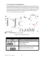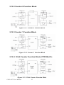
1
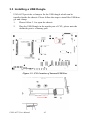
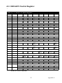
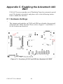
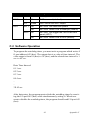
UNO-4672 Intel Pentium M/Celeron M Fanless Box PC with 6 x LAN, 10 x COM, 8 x DI, 8 x DO, PC/104+ User Manual Copyright This document is copyrighted, © 2009. All rights are reserved. The original manufacturer reserves the right to make improvements to the products described in this manual at any time without notice. No part of this manual may be reproduced, copied, translated or transmitted in any form or by any means without the prior written permission of the original manufacturer. Information provided in this manual is intended to be accurate and reliable. However, the original manufacturer assumes no responsibility for its use, nor for any infringements upon the rights of third parties that may result from such use. Acknowledgements Intel, Pentium and Celeron are registered trademarks of Intel Corp. Microsoft Windows and MS-DOS are registered trademarks of Microsoft Corp. All other product names or trademarks are properties of their respective owners. Support For more information on this and other Advantech products, please visit our websites at: http://www.advantech.com For technical support and service, please visit our support website at: http://www.advantech.com/support/ This manual is for UNO-4672. Part No. 2003467200 1st Edition Printed in Taiwan February 2009 UNO-4672 User Manual ii Product Warranty (2 years) Advantech warrants to you, the original purchaser, that each of its products will be free from defects in materials and workmanship for two years from the date of purchase. This warranty does not apply to any products that have been repaired or altered by persons other than repair personnel authorized by Advantech, or which have been subject to misuse, abuse, accident or improper installation. Advantech assumes no liability under the terms of this warranty as a consequence of such events. Because of Advantech high quality-control standards and rigorous testing, most of our customers never need to use our repair service. If an Advantech product is defective, it will be repaired or replaced at no charge during the warranty period. For out-of-warranty repairs, you will be billed according to the cost of replacement materials, service time and freight. Please consult your dealer for more details. If you think you have a defective product, follow these steps: Step 1. Collect all the information about the problem encountered. (For example, CPU speed, Advantech products used, other hardware and software used, etc.) Note anything abnormal and list any onscreen messages you get when the problem occurs. Step 2. Call your dealer and describe the problem. Please have your manual, product, and any helpful information readily available. Step 3. If your product is diagnosed as defective, obtain an RMA (return merchandize authorization) number from your dealer. This allows us to process your return more quickly. Step 4. Carefully pack the defective product, a fully completed Repair and Replacement Order Card and a photocopy proof of purchase date (such as your sales receipt) in a shippable container. A product returned without proof of the purchase date is not eligible for warranty service. Step 5. Write the RMA number visibly on the outside of the package and ship it prepaid to your dealer. iii CE This product has passed the CE test for environmental specifications. Test conditions for passing included the equipment being operated within an industrial enclosure. In order to protect the product from being damaged by ESD (Electrostatic Discharge) and EMI leakage, we strongly recommend the use of CE-compliant industrial enclosure products. FCC Class A This equipment has been tested and found to comply with the limits for a Class A digital device, pursuant to Part 15 of the FCC Rules. These limits are designed to provide reasonable protection against harmful interference when the equipment is operated in a commercial environment. This equipment generates, uses and can radiate radio frequency energy and, if not installed and used in accordance with the instruction manual, may cause harmful interference to radio communications. Operation of this equipment in a residential area is likely to cause harmful interference in which case the user will be required to correct the interference at his own expense. Technical Support and Assistance Step 1. Visit the Advantech web site at www.advantech.com/support where you can find the latest information about the product. Step 2. Contact your distributor, sales representative, or Advantech's customer service center for technical support if you need additional assistance. Please have the following information ready before you call: - Product name and serial number - Description of your peripheral attachments - Description of your software (OS, version, software, etc.) - A complete description of the problem - The exact wording of any error messages UNO-4672 User Manual iv Safety Instructions 1. Read these safety instructions carefully. 2. Keep this User's Manual for later reference. 3. Disconnect this equipment from any AC outlet before cleaning. Use a damp cloth. Do not use liquid or spray detergents for cleaning. 4. For plug-in equipment, the power outlet socket must be located near the equipment and must be easily accessible. 5. Keep this equipment away from humidity. 6. Put this equipment on a reliable surface during installation. Dropping it or letting it fall may cause damage. 7. The openings on the enclosure are for air convection. Protect the equipment from overheating. DO NOT COVER THE OPENINGS. 8. Make sure the voltage of the power source is correct before connecting the equipment to the power outlet. 9. Position the power cord so that people cannot step on it. Do not place anything over the power cord. 10. All cautions and warnings on the equipment should be noted. 11. If the equipment is not used for a long time, disconnect it from the power source to avoid damage by transient overvoltage. 12. Never pour any liquid into an opening. This may cause fire or electrical shock. 13. Never open the equipment. For safety reasons, the equipment should be opened only by qualified service personnel. 14. If one of the following situations arises, get the equipment checked by service personnel: a. The power cord or plug is damaged. b. Liquid has penetrated into the equipment. c. The equipment has been exposed to moisture. d. The equipment does not work well, or you cannot get it to work according to the user's manual. e. The equipment has been dropped and damaged. f. The equipment has obvious signs of breakage. 15. DO NOT LEAVE THIS EQUIPMENT IN AN ENVIRONMENT WHERE THE STORAGE TEMPERATURE MAY GO BELOW v 20° C (-4° F) OR ABOVE 55° C (131° F). THIS COULD DAMAGE THE EQUIPMENT. THE EQUIPMENT SHOULD BE IN A CONTROLLED ENVIRONMENT. 16. CAUTION: DANGER OF EXPLOSION IF BATTERY IS INCORRECTLY REPLACED. REPLACE ONLY WITH THE SAME OR EQUIVALENT TYPE RECOMMENDED BY THE MANUFACTURER, DISCARD USED BATTERIES ACCORDING TO THE MANUFACTURER'S INSTRUCTIONS. The sound pressure level at the operator's position according to IEC 7041:1982 is no more than 70 dB (A). DISCLAIMER: This set of instructions is given according to IEC 704-1. Advantech disclaims all responsibility for the accuracy of any statements contained herein. Safety Precaution - Static Electricity Follow these simple precautions to protect yourself from harm and the products from damage. • To avoid electrical shock, always disconnect the power from your PC chassis before you work on it. Don't touch any components on the CPU card or other cards while the PC is on. • Disconnect power before making any configuration changes. The sudden rush of power as you connect a jumper or install a card may damage sensitive electronic components. UNO-4672 User Manual vi Contents Chapter Chapter 1 Overview .......................................................... 2 1.1 1.2 1.3 1.4 Introduction ....................................................................... 2 Hardware Specifications ................................................... 5 Safety Precautions ............................................................. 7 Chassis Dimensions........................................................... 8 1.5 Packing List....................................................................... 8 Figure 1.1:Chassis Dimensions ...................................... 8 2 Hardware Functionality ............................... 10 2.1 2.2 Overview ......................................................................... 10 Figure 2.1:UNO-4672 Front Panel .............................. 10 Figure 2.2:UNO-4672 Rear Panel ............................... 10 LED Indicators ................................................................ 11 2.2.1 2.2.2 2.2.3 2.2.4 System Status Indicators .............................................. 11 Table 2.1:Definition of System Status Indicators ........ 11 LAN Status Indicators ................................................. 12 Table 2.2:Definition of LAN Status Indicators ........... 12 Serial Communication Status Indicators ..................... 12 Table 2.3:Definition of Serial COM Status Indicators 12 Digital Input/Output Status Indicators ......................... 13 Table 2.4:Definition of DI/DO Status Indicators ......... 13 2.3 Power Input ..................................................................... 13 2.4 RS-232 Interface (COM1,COM2)................................... 15 2.5 RS-232/422/485 Interface (COM3~COM10) ................. 15 Table 2.5:AC/DC Power Input .................................... 13 Table 2.6:AC/DC Power Input Function Introduction 14 Table 2.7:IRQ and I/O Address for COM1,COM2 ..... 15 2.5.1 2.5.2 2.5.3 2.5.4 2.5.5 2.5.6 2.5.7 2.6 2.7 2.8 OXmPCI954 UARTs with 128 bytes FIFO ................. 15 RS-422/485 Detection .................................................. 15 Automatic Data Flow Control Function for RS-485 ... 15 Terminal Resistor (JP9~JP16) ..................................... 16 Table 2.8:Jumper setting of terminal resistor .............. 16 Table 2.9:Mapping table of Jumper/DIP for COM port .. 16 Figure 2.3:COM Port Related Jumper/Switch Locations 17 RS-232/422/485 Selection ........................................... 18 Figure 2.4:RS-422/485 Jumper Setting ....................... 18 Figure 2.5:RS-232 Jumper Setting ............................... 18 RS-485 Auto Flow & RS-422 Master/Slave Modes .... 19 Table 2.10:SW2 DIP Setting ....................................... 19 Redundant RS-422 Matter ........................................... 19 Table 2.11:Mapping table of switches for COM port .. 20 LAN: Ethernet Connector ............................................... 20 USB Ports........................................................................ 21 VGA Display................................................................... 21 vii Table of Contents 2.9 2.10 2.11 2.12 Battery Backup SRAM.................................................... 21 2.9.1 Lithium Battery Specifications .................................... 22 Figure 2.6:SRAM Lithium Battery Location................ 22 Onboard Isolated Digital Input........................................ 22 2.10.1 Pin Assignments .......................................................... 22 Figure 2.7:Digital Input Connector Pin Assignments .. 23 Table 2.12:Digital Input Connector Signal Description .. 23 2.10.2 Isolated Inputs .............................................................. 23 Figure 2.8:Isolated Digital Input Connection .............. 24 2.10.3 Interrupt Function of the DI Signals ............................ 24 2.10.4 IRQ Level .................................................................... 24 2.10.5 Interrupt Control Register ............................................ 25 Table 2.13:Interrupt Control Register Bit Map ........... 25 2.10.6 Interrupt Enable Control Function ............................... 25 Table 2.14:Interrupt Disable/Enable Control ............... 25 2.10.7 Interrupt Triggering Edge Control ............................... 26 Table 2.15:Interrupt Triggering Edge Control ............. 26 2.10.8 Interrupt Flag Bit ......................................................... 26 Table 2.16:Interrupt Flag Bit Values ........................... 26 Onboard Isolated Digital Output ..................................... 27 2.11.1 Pin Assignments .......................................................... 27 Figure 2.9:Digital Output Connector Pin Assignments 27 Table 2.17:Digital Output Connector Signals .............. 27 2.11.2 Power On Configuration .............................................. 28 Figure 2.10:Location of CN40 ..................................... 28 Table 2.18:Digital Output Power On Configuration ... 28 2.11.3 Isolated Outputs ........................................................... 29 Onboard Isolated Counter/Timer .................................... 30 2.12.1 Counter/Timer Control Register .................................. 30 Table 2.19:Counter/Timer Control Register Bit Map .. 31 2.12.2 Counter 0 Function Block ............................................ 32 Figure 2.11:Counter 0 Function Block ........................ 32 2.12.3 Counter 1 Function Block ............................................ 32 Figure 2.12:Counter 1 Function Block ........................ 32 2.12.4 32-bit Counter Function Block (CTR32Set=1) .......... 32 Figure 2.13:32-bit Counter Function Block ................. 32 2.12.5 Counter Clock Source .................................................. 33 Table 2.20:Counter Clock Source Control Bit ............. 33 2.12.6 Counter Internal Clock ................................................. 33 Table 2.21:Counter Internal Clock Control Bit ........... 33 2.12.7 Counter Gate Source .................................................... 33 Table 2.22:Counter Gate Source Control Bit ............... 33 2.12.8 Counter Output Destination ......................................... 34 Table 2.23:Counter Output Destination Control Bit .... 34 2.12.9 Counter Interrupt Flag ................................................. 34 Table 2.24:Counter Interrupt Flag Control Bit ............ 34 2.12.10 Cascaded 32-bit Counter .............................................. 35 UNO-4672 User Manual viii Chapter Table 2.25:32-bit Counter Control Bit ......................... 35 2.13 LED and Buzzer for System Diagnosis........................... 35 2.14 PC/104+........................................................................... 37 Table 2.26:LED & Buzzer Control Register ............... 35 Table 2.27:Programmable LED Control Bit ................ 36 Table 2.28:Programmable Buzzer Control Bit ............ 36 Figure 2.14:PC104+ Power Selection.......................... 37 Figure 2.15:CN14 Location ......................................... 37 3 Initial Setup.................................................... 40 3.1 3.2 Configuration .................................................................. 40 Install a CompactFlash Card ........................................... 41 3.3 Installing a USB Dongle ................................................. 42 3.4 Installing a Hard Disk ..................................................... 43 3.5 3.6 Installation on Rack......................................................... 45 BIOS Setup and System Assignments ............................ 46 Figure 3.1:CompactFlash Card Slot Location ............. 41 Figure 3.2:CN3 Location of Internal USB Port ........... 42 Figure 3.3:SATA Signal and Power Connector Location 44 Appendix A System Settings & Pin Assignments ............ 48 A.1 System I/O Address & Interrupt Assignments................ 48 A.2 RS-232/422/485 Serial Ports (COM1~COM10)............. 50 A.3 USB Connectors (USB1~USB2) .................................... 52 A.4 VGA Display Connector ................................................. 52 A.5 UNO-4672 Control Register ........................................... 53 Table A.1: UNO-4672 System I/O Ports ...................... 48 Table A.3:RS-232 Serial Ports COM1~2 ..................... 50 Table A.4:RS-232/422/485 Serial Ports (COM3~10) .. 51 Table A.5:USB Connector Pin Assignments................ 52 Table A.6:VGA Adaptor Cable Pin Assignments ........ 52 Table A.7:UNO-4672 Control Register ....................... 53 Appendix B Watchdog Timer Programming................... 56 B.1 UNO-4672....................................................................... 56 Appendix C Enabling the Advantech 443 WDT.............. 60 C.1 Hardware Settings ........................................................... 60 C.2 Software Operation ......................................................... 61 Figure C.1:Location of CN45 and SW4 for Standard 443 WDT 60 Table C.1:CN45 and SW4 Descriptions ...................... 61 ix Table of Contents UNO-4672 User Manual x CHAPTER 1 2 Overview This chapter provides an overview of UNO-4672’s specifications. Sections include: • Introduction • Hardware Specifications • Safety Precautions • Chassis Dmensions • Packing List Chapter 1 Overview 1.1 Introduction UNO-4672 is an embedded Application Ready Platform (ARP) that can shorten development time and offers rich networking interfaces to fulfill extensive needs. UNO-4672 is designed to be a total solution for network enabled Application Ready Platforms. Leveraging field-approved and worldwide approved real-time OS technology, Advantech UNO-4672 series provides a Windows CE .NET and Windows XP Embedded ready solution, and supports several standard networking interfaces, such as Ethernet, RS-232/422/485 and more. Because of its openness, great expansion capability and reliable design (fanless and diskless), the UNO-4672 series are ideal embedded platforms for implementing custom applications for diverse applications. Target on Data Server and Communication Gateway in Substations Advantech UNO-4672 has been defined and designed to be compliant with IEC-61850-3, which has been defined as an international hardware standard of communication network and system in power substations. In modern power substation, this standard facilitate the management to large number of devices and enable the various devices to communicate with one another. UNO-4672 is a ready and certified platform to serve all these requirement. Open Architecture Designed for Automation For applications demanding customized control, an UNO-4672 that uses more flexible, off-the-shelf technology is a better option. UNO-4672 uses off-the-shelf components such as an x86 processor, an Ethernet chip set, CompactFlash., and DRAM. At the same time, the UNO-4672 unit can broadcast the process data through the Ethernet and share the data with operators and managers. By using off-the-shelf components, machine builders can customize the control scheme they use for other machines that require multiple inputs, optimized control, or Ethernet communication. So, UNO-4672 offers the I/O connectivity of PCs with options like: 6 x Ethernet ( 2 x 10/100/1000 Base-T, 4 x 10/100 Base-T ), 10 x Serial ports ( 2 x RS-232, 8 x RS-232/422/485 ), 4 x USB ports ( 1 x Front, 2 x Rear, 1 x Internal ), 2 x CompactFlash and VGA interface for display panels. UNO-4672 User Manual 2 Robust IO Isolate System from Electrical Noise UNO-4672 is designed for the applications in substation where is supposed to have certain electric interference. Equipping with isolated power, isolated DI/DO and isolated communication ports, UNO-4672 has high resistance toward electrical noise. It has been proved not only can work well in substation but also suitable for any harsh applicaitons An Industry-Proven Design Industrial applications require controllers with high-vibration specifications and a wide temperature range. Controllers in industrial environments require flexible and stable mounting, and many machine builders underestimate the need for rugged controllers because their applications are mounted in an industrial enclosure. UNO-4672 has a special design without the weaknesses of a standard PC. No fan, and no HDD prevent dust and vibration problems. With a smart mechanical design, UNO-4672 can meet 50 G shock (with CompactFlash ), 2 G vibration (with CompactFlash), up to 55° C operating temperature (tested under 100% CPU loading ) and almost anything an industrial environments demand. Designed to Fit Comfortably Into Racks In completely new packaging, UNO-4672 has standard 2U rack size as 440 x 220 x 88 mm (W x H x D) could fit your rack. The rear IO connection and indicator LEDs on the front panel for all ports and modes highly simplify monitoring for operation and maintenance in the rack. You could easily mount UNO-4672 on rack, manage all UNOs in one rack and easily develop your application on rack. Flexible Networking Options The Advantech UNO-4672 offers two ways to connect to a network: Ethernet and Modem. The six built-in Ethernet ports provide high-speed networking capability up to 1 Gbps. And through UNO-4672’s isolated serial COM ports, you could link industrial modems to offer the most popular and easiest networking method by PSTN. UNO-4678 provides 2 channels full 9-pins standard RS-232 isolated serial COM ports and 8 channels 5-pins isolated serial COM ports with RS-232/422/485 selectable. These ports all equip with surge and isolation protection up to 2000 VDC ,protecting your system from abrupt high voltage attack and accident or damage in harsh environments. 3 Chapter 1 Popular Operating Systems and Rapid Application Development The Advantech UNO-4672 supports the popular off-the-shelf Microsoft Windows 2000/NT/XP operating systems and the Linux operating system. UNO-4672 also features pre-built Microsoft Windows XP embedded or Windows CE solutions offering a pre-configured image with optimized onboard device drivers. Microsoft Windows CE and XP Embedded are compact, highly efficient, and real-time operating systems that are designed for embedded systems without a HDD. There is no need to waste time and energy on developing onboard device drivers or using the Platform Builder to build a custom Windows CE image, they have all been done for the Advantech UNO-4672 series! Through the built-in runtime library and Software Development Kit (SDK), the UNO-4672 series leverages your existing Windows-based programming skills to rapidly develop applications. UNO-4672 User Manual 4 1.2 Hardware Specifications General Certifications IEC-61850-3, CE, FCC Class A Dimensions (W x D x H) 2U (440 x 220 x 88 mm) (17.3” x 8.6” x 3.4”) Enclosure SECC Mounting Rack Power Consumption 45 W (Typical) Power Input AC: 90 - 250 VAC (47~400Hz) or DC: 106 - 250 VDC With isolation protection Weight 6.0 kg OS Support Windows XP Embedded SP2, Windows 2000/ XP, Windows CE .NET 6.0, Linux System Hardware CPU Pentium M 1.4 GHz / Celeron M 1 GHz Indicators LEDs for Power, Storage, Alarm for battery backup SRAM, Diagnosis (programmable), LAN (Active, Status) and Serial (Tx, Rx) Memory 1 GB DDR DRAM Storage SSD: 2 x internal type I/II CompactFlash slots HDD: One built-in 2.5" SATA HDD bracket Display DB15 VGA connector, 1600x1200 @ 85Hz PC/104 Slot PC/104+ supports +3.3V & 5V power Watchdog Timer Programmable 256 level timer interval, from 1 to 255 sec Battery Backup SRAM 512 KB 5 Chapter 1 I/O Interface Serial Ports 2 x DB-9 connectors with 9-wired RS-232 8 x screw terminals with 5-wired RS-232/422/485 selectable Automatic RS-485 data flow control 2000 VDC surge protection & isolation Serial Port Speed COM1,COM2: RS-232: 50~115.2 kbps COM3~COM10: RS-232: 50~230.4 kbps RS-422/485: 50~921.6 kbps (Max.) LAN 2 x 10/100/1000 Base-T RJ-45 ports 4 x 10/100 Base-T RJ-45 ports USB 4 x USB ports, UHCI, Rev. 2.0 compliant (1 x front, 2 x rear and 1 x internal ports) Digital Input 8-ch wet contact DI Logic 0: 0 ~ 3 VDC; Logic 1: 10 ~ 50 VDC 2,000 VDC isolation, 2,000 VDC ESD protection 70 VDC over-voltage protection Interrupt handling: IRQ 7 Photo couple response: 100 ?s Digital Output 8-ch DO 2,000 VDC isolation and 200 mA max/channel sink current Keep output status after system hot reset 5 ~ 40 VDC output range and 10 kHz speed Timer/Counter Counter Source : DI1 & DI3, jumper selected Pulse output : DO2 & DO3, jumper selected Can be cascaded as one 32-bit counter/timer Support down counting, preset counting value Timer time base : 100 kHz, 10 kHz, 1 kHz, 100Hz UNO-4672 User Manual 6 Environment Humidity 95% @ 40° C (non-condensing) Operating Temperature -20 ~ 55° C (-4 ~ 131° F) (100% CPU load) -20 ~ 65°C (-4 ~ 149° F) (50% CPU load) Shock Protection IEC 68 2-27 CompactFlash: 50 G, half sine, 11 ms HDD: 20 G, half sine, 11 ms Vibration Protection IEC 68 2-64 (Random 1 Oct./min, 1hr/axis.) CompactFlash: 2 Grms @ 5 ~ 500 Hz, HDD: 1 Grms @ 5 ~ 500 Hz 1.3 Safety Precautions The following,messages informs how to make each connection. In most cases, you will simply need to connect a standard cable. Warning! Always disconnect the power cord from your chassis whenever you are working on it. Do not connect while the power is on. A sudden rush of power can damage sensitive electronic components. Only experienced electronics personnel should open the chassis. Caution! Always ground yourself to remove any static electric charge before touching UNO-4672. Modern electronic devices are very sensitive to static electric charges. Use a grounding wrist strap at all times. Place all electronic components on a static-dissipative surface or in a static-shielded bag. Attention! If DC voltage is supplied by an external circuit, please put a protection device in the power supply input port. 7 Chapter 1 1.4 Chassis Dimensions 220 440 TOP VIEW 20 20 467 32 6 76 88 6 459 FRONT VIEW LEFT VIEW RIGHTVIEW UNO-4672 BACK VIEW Figure 1.1: Chassis Dimensions 1.5 Packing List The accessory package of UNO-4672 contains the following items: (A) UNO-4672 (B) 2 x rack mounting kit (C) 12 x screw for rack mount kit (D) 2 x front handles (E) 4 x screws for front handles (F) 6 x 10-pins green screw terminals (G) 1 x SATA signal cable (H) 1 x SATA power cable (I) 4 x screws for SATA HDD installation (J) 1x clamp for USB dongle (K) 2x screws for USB clamp (L) UNO series Driver and Utility DISC (M) 1 x warranty card UNO-4672 User Manual 8 CHAPTER 2 2 Hardware Functionality This chapter shows how to setup the UNO-4672’s hardware functions, including connecting peripherals, setting switches and indicators. Sections include: • Overview • LED Indicators • Power Input • RS-232 Interface • RS-232/422/485 Interface • LAN / Ethernet Connector • USB Ports • VGA Display • Battery Backup SRAM • Onboard Isolated Digital Input • Onboard Isolated Digital Output • Onboard Isolated Counter/Timer • LED & Buzzer for System Diagnosis • PC/104+ Chapter 2 Hardware Functionality 2.1 Overview The following two figures show the indicators and connectors on UNO4672. The following sections give you detailed information about function of each peripheral. Figure 2.1: UNO-4672 Front Panel Figure 2.2: UNO-4672 Rear Panel UNO-4672 User Manual 10 2.2 LED Indicators The LEDs in the front panel can be divided into 4 groups. 2.2.1 System Status Indicators Table 2.1: Definition of System Status Indicators Item LED Status Description 1 PWR Green System power is on Off System power is off 2 IDE Green Data being received/ transmitted between storage devices Off No Data being received/ transmitted between storage devices WDT (reserved) Green 443 WDT trigger the LED for alarm Off Default 4 BTR Red Battery for SRAM should be replaced Off Status of battery for SRAM is OK 5 DIAG Red/ LED turn on by program Flicking 3 6 LED (Port 0 ~ 7) Off LED turn off by program (default) Green LED turn on by program Off LED turn off by program (default) 11 Chapter 2 2.2.2 LAN Status Indicators Table 2.2: Definition of LAN Status Indicators Item LED Status Description 1 LAN/Link ( Port 1~2) Orange 1 Gbps network link Green 100Mbps network link Off 10Mbps network link or invalid network link LAN/Link (Port 3~6) Green 100Mbps network link Off 10Mbps network link or invalid network link LAN/Active (Port 1~6) Orange Ethernet date being received/ transmitted Off No Ethernet data being received/ transmitted 2 3 2.2.3 Serial Communication Status Indicators Table 2.3: Definition of Serial COM Status Indicators Item LED Status Description 1 COM/Rx (Port 1~10) Green Serial port data being received Off No data being received COM/Tx (Port 1~10) Orange Serial port data being transmitted Off No data being transmitted 2 UNO-4672 User Manual 12 2.2.4 Digital Input/Output Status Indicators Table 2.4: Definition of DI/DO Status Indicators Item LED Status Description 1 DO(Port 0~7) Green DO port is activated Off DO port is inactivated 2 DI(Port 0~7) Orange DI port has signal input Off DI port has no signal input 2.3 Power Input The UNO-4672 support AC/DC power input to fulfill the need of field site. Following table shows the specification of the power input. Table 2.5: AC/DC Power Input AC/DC Volt. Range Power Rating Connector Type AC 90-250V 1.6-0.8A, 47-400 Hz 3P Power Jack DC 106-250V 1.6-0.8A 3Pin Screw Terminal 13 Chapter 2 The function of each part is described as below: Table 2.6: AC/DC Power Input Function Introduction Item Function Description 1 Power jack for AC power input 2 Fuse for AC power input; one backup fuse inside 3 AT power switch for AC/DC power input 4 Switch for selecting AC or DC power input 5 Screw terminal for DC power input 6 Screw for connecting chassis to field ground UNO-4672 User Manual 14 2.4 RS-232 Interface (COM1,COM2) The UNO-4672 offers two standard RS-232 serial communication interface port: COM1 and COM2. Please refer to A.2 for pin assignments. The IRQ and I/O address of COM1 and COM2 are listed below: Table 2.7: IRQ and I/O Address for COM1,COM2 COM No. IRQ I/O Address COM1 IRQ4 3F8H COM2 IRQ3 2F8H 2.5 RS-232/422/485 Interface (COM3~COM10) The UNO-4672 offers eight RS-232/422/485 serial communication interface ports: COM3 to COM10. Please refer to Appendix A.2 for their pin assignments. The default setting of COM3 to COM10 are RS-232. 2.5.1 OXmPCI954 UARTs with 128 bytes FIFO Advantech UNO-4672 comes with Oxford OXmPCI954 UARTs containing 128 bytes FIFOs. 2.5.2 RS-422/485 Detection In RS-422/485 mode, UNO-4672 automatically detects signals to match RS-422 or RS-485 networks. (No jumper change required) 2.5.3 Automatic Data Flow Control Function for RS-485 In RS-485 mode, UNO-4672 automatically detects the direction of incoming data and switches its transmission direction accordingly. So no handshaking signal (e.g. RTS signal) is necessary. This lets you conveniently build an RS-485 network with just two wires. More importantly, application software previously written for half duplex RS-232 environments can be maintained without modification. 15 Chapter 2 2.5.4 Terminal Resistor (JP9~JP16) The onboard termination resistor (120 ohm) for COM3~COM10 can be used for long distance transmission or device matching. (Default Open.) Please also refer to Table 2.9 for the mapping table of Jumper and COM port. Table 2.8: Jumper setting of terminal resistor JPx Description 3 1 4 2 3 1 4 2 Add termial resistor on Tx+/Tx- of RS-422 or Data+/Dataof RS-485 Add termial resistor on Rx+/Rx- of RS-422 Table 2.9: Mapping table of Jumper/DIP for COM port COM port Jumper for RS-232 and RS-422/485 selection SW2 DIP switch for Auto-flow control Jumper for Terminal Resistor COM3 JP2 DIP1 JP10 COM4 JP3 DIP2 JP11 COM5 JP1 DIP3 JP9 COM6 JP4 DIP4 JP12 COM7 JP6 DIP5 JP14 COM8 JP7 DIP6 JP15 COM9 JP5 DIP7 JP13 COM10 JP8 DIP8 JP16 UNO-4672 User Manual 16 Figure 2.3: COM Port Related Jumper/Switch Locations 17 Chapter 2 2.5.5 RS-232/422/485 Selection COM3 ~ COM10 support RS-232, RS-422 and RS-485 interfaces. The system detects RS-422 or RS-485 signals automatically in RS-422/485 mode. To select between RS-422/485 and RS-232 for COM3 ~ COM10, adjust JP1 ~ JP8 and Table 2.9 shows the mapping table. Jumper settings for RS-422/485 interface: (JP1 ~ JP8) Figure 2.4: RS-422/485 Jumper Setting Jumper settings for RS-232 interface: (Default setting) (JP1 ~ JP8) Figure 2.5: RS-232 Jumper Setting UNO-4672 User Manual 18 2.5.6 RS-485 Auto Flow & RS-422 Master/Slave Modes You can set the “Auto Flow Control” mode of RS-485 or “Master/Slave” mode of RS-422 by using the SW2 DIP switch for COM3~COM10. Please also refer to Table 2.9 for the COM port mapping with the DIP. In RS-485, if the switch is set to “Off”, the driver automatically senses the direction of the data flow and switches the direction of transmission. No handshaking is necessary. In RS-422, if DIP switch is set to “On,” the driver is always enabled, and always in high or low status. Please refer below for the default setting. Table 2.10: SW2 DIP Setting SW2 Status Description ON RS-422: Master mode RS-485: N/A OFF(Default) RS-422: Slave mode RS-485: Auto flow control 2.5.7 Redundant RS-422 Matter In the occasion that UNO-4672 RS-422 ports need to act as multi-master in parallel with other RS-422 master ports. Because of the auto detection function, the TX port will also receive data from other RS-422 master. To avoid this situation in this kind of application, user can use SW5~SW12 to turn it off, then no data will be received from TX port. Please refer to the Table 2.11 for the COM port mapping and refer to Figure 2.3 for the location. 19 Chapter 2 Table 2.11: Mapping table of switches for COM port COM port Switches Status COM3 SW6 COM4 SW7 COM5 SW5 COM6 SW8 COM7 SW10 COM8 SW11 COM9 SW9 COM10 SW12 ON: Normal (default) OFF: RS-422 multi-master 2.6 LAN: Ethernet Connector The UNO-4678 is equipped with 2 Intel 82541 PI Gigabit Ethernet Controller which are compliant with IEEE802.3 1000Base-T, 100Base-TX and 10Base-T (802.3, 802.3u and 802.3ab). And it is also equipped with 4 Realtek RTL8100CL Network controllers which are compliant with IEEE 802.3u 10/ 100Base-T CSMA/CD standards. The Ethernet port provides a standard RJ-45 jack on board, and LED indicators on the front side to show its Link and Active status. Please note these LAN controllers all use PCI resource, the bandwidth or throughput may be restricted by the PCI bandwidth. UNO-4672 User Manual 20 2.7 USB Ports The UNO-4672 provides four USB interface connectors, which provide complete Plug & Play and hot swapping for up to 127 external devices. The USB interface complies with USB UHCI, Rev. 2.0 compliant. The USB interface can be disabled in the system BIOS setup. UNO-4672 provides 1 USB port on the front panel, and 2 USB port on the rear panel. It also provides 1 USB port inside the chassis for USB dongle key. 2.8 VGA Display The UNO-4672 provides a VGA controller (Intel 852 GME, supports a single 1.5V accelerated graphics port interface) for a high resolution VGA interface. CRT Mode: 1280 x 1024 @ 32bpp (60Hz), 1024 x 768 @ 32bpp (85Hz); LCD/Simultaneous Modes: 1280 x 1024 @ 16bpp(60Hz), 1024 x 768 @16bpp(60Hz) and up to 32 MB shared memory. 2.9 Battery Backup SRAM UNO-4672 provides 512 KB of battery backup SRAM. This ensures that you have a safe place to store critical data. You can now write software applications without being concerned that system crashes will erase critical data from the memory. There is a BTR LED in the front panel of the UNO-4672, please replace the lithium battery with a new one if the BTR LED is activated. 21 Chapter 2 2.9.1 Lithium Battery Specifications • Type: BR2032 (Using CR2032 is NOT recommended) • Output voltage: 3 VDC • Location: the backside of UNO-4672 board. (BH1 is for real time clock, BH2 is for SRAM) Figure 2.6: SRAM Lithium Battery Location 2.10 Onboard Isolated Digital Input The UNO-4672 has 8 isolated DI channels designated DI0~DI7. 2.10.1 Pin Assignments The connector type of UNO-4672 is plug-in screw terminal block that enables you to connect to field I/O devices directly without additional accessories. Figure 2.7 and Table 2.12 shows its pin assignment as well as signal description. UNO-4672 User Manual 22 Figure 2.7: Digital Input Connector Pin Assignments Table 2.12: Digital Input Connector Signal Description Signal Name Reference Direction Description DI <0...7> I.GND I.GND - Input - Isolated DI signals DI isolated ground 2.10.2 Isolated Inputs Each of isolated digital input channels accepts 0 ~ 50 VDC voltage inputs, and accepts bi-directional input. The voltage range is -3 ~ 3 VDC for logic 0 (low), -50 ~ -10 VDC and 10 ~ 50 VDC for logic 1 (high). It means that you can apply positive or negative voltage to an isolated input pin (Vin). All channels share two common pins (I.GND). Figure 2.8 shows how to connect an external input source to an UNO-4672 isolated input channel. Please note that DI0 and DI2 may be configured as gate control pins of Counter 0 and Counter 1; While DI1 and DI3 may be configured as input pins of Counter 0 and Counter 1. 23 Chapter 2 Figure 2.8: Isolated Digital Input Connection 2.10.3 Interrupt Function of the DI Signals DI0 and DI1 can be used to generate hardware interrupts. Users can setup the configuration of them by programming the interrupt control register. The channels are connected to the interrupt circuitry. Users can disable/ enable interrupt function, select trigger type or latch the port data by setting the Interrupt Control Register of the UNO-4672. When the interrupt request signals occur, then the software will service these interrupt requests by ISR (Interrupt Service Routine). The multiple interrupt sources provide the card with more capability and flexibility. 2.10.4 IRQ Level The IRQ level is by default set by the system BIOS. IRQ 7 is reserved for DI interrupt and counter interrupt. UNO-4672 User Manual 24 2.10.5 Interrupt Control Register Table 2.13: Interrupt Control Register Bit Map Base Address 202H 7 R/W 6 5 4 3 2 1 0 Interrupt Enable Control/Status Register DI1EN DI0EN 203H 207H R/W R/W Interrupt Triggering Edge Control/Status Register DI1TE DI0TE DI1F DI0F Interrupt Flag/Clear Register The Interrupt Control Register controls the function and status of each interrupt signal source. Table 2.13 shows the bit map of the Interrupt Control Register. The register is readable/writeable register. While being written, it is used as a control register; and while being read, it is used as a status register. DI0EN & DI1EN: DI0 & DI1 Interrupt disable/enable control bit DI0TE & DI1TE: DI0 & DI1 Interrupt triggering edge control bit DI0F & DI1F: DI0 & DI1 interrupt flag bit 2.10.6 Interrupt Enable Control Function Table 2.14: Interrupt Disable/Enable Control DI0EN & DI1EN Interrupt Disable/Enable Control 0 Disable 1 Enable The user can choose to enable or disable the interrupt function by writing its corresponding value to the interrupt disable/enable control bit in the interrupt control register, as shown in Table 2.14. 25 Chapter 2 2.10.7 Interrupt Triggering Edge Control The interrupt can be triggered by a rising edge or a falling edge of the interrupt signal, as determined by the value in the interrupt triggering edge control bit in the interrupt control register, as shown in Table 2.15. Table 2.15: Interrupt Triggering Edge Control DI0TE & DI1TE Triggering edge of interrupt signal 0 Falling edge trigger 1 Rising edge trigger 2.10.8 Interrupt Flag Bit The interrupt flag bit is a flag indicating the status of an interrupt. It is a readable/writable bit. To find the status of the interrupt, you have to read the bit value. To clear the interrupt, you have to write “1” to this bit. This bit must first be cleared to service the next coming interrupt. Table 2.16: Interrupt Flag Bit Values DI0F & DI1F Read Write Interrupt Status 0 No interrupt 1 Interrupt occur 0 Don’t care 1 Clear interrupt Note: UNO-4672 provides built-in examples to show how to deliver digital input functionality. Refer to console mode examples in C:\Program Files\Advantech\UNO\UNO_IsaDIO\Examples\Console. (Please install DI/O driver from the UNO CD to use these examples) UNO-4672 User Manual 26 2.11 Onboard Isolated Digital Output The UNO-4672 has 8 isolated DO channels designated DO0 ~ DO7. 2.11.1 Pin Assignments The connector type of UNO-4672 is plug-in screw terminal block that enables you to connect to field I/O devices directly without additional accessories. Figure 2.9 and Table 2.17 show its pin assignment as well as signal description. Figure 2.9: Digital Output Connector Pin Assignments Table 2.17: Digital Output Connector Signals Signal Name Reference DO <0...7> O.GND COM GND - Direction Description Output Isolated DO signals - DO isolated ground DO_COM as using inductance load 27 Chapter 2 2.11.2 Power On Configuration Default configuration after power on or hardware reset is to set all the isolated digital output channels to open status (the current of the load can’t be sink) so that users need not worry about damaging external devices during system startup or reset. When the system is hot reset, then the status of isolated digital output channels are selected by jumper CN40. Table 2.18 shows the configuration of jumper CN40. Figure 2.10: Location of CN40 Table 2.18: Digital Output Power On Configuration CN40 Power on configuration after hot reset Set to "Open" status Default setting Keep last status after hot reset UNO-4672 User Manual 28 2.11.3 Isolated Outputs Each of isolated output channels comes equipped with a Darlington transistor. All output channels share common emitters. Please note that if an external voltage (5 ~ 40 VDC) is applied to an isolated output channel while it is being used as an output channel, the current will flow from the external voltage source to the UNO-4672. Please take care that the current through each DO pin not exceed 200 mA. Figure below shows how to connect an external output load to the UNO-4672 isolated outputs. Please note that DO2 and DO3 may be configured as output pins of Counter 0 and Counter 1. Note: UNO-4672 provides built-in examples to show how to deliver digital output functionality. Refer to console mode examples in C:\Program Files\Advantech\UNO\UNO_IsaDIO\Examples\Console. (Please install DI/O driver from the UNO CD to use these examples) 29 Chapter 2 2.12 Onboard Isolated Counter/Timer The UNO-4672 uses one 82C54 programmable timer/counter chip that includes three independent 16-bit down counters: counter 0, counter 1 and counter 2. Counter 0 and counter 1 are for users, and counter 2 is specified for the system and can’t be used by user. Each counter has clock input, gate input and pulse output. They can be programmed to count from 2 up to 65535 or cascaded into one 32-bit counter. The UNO-4672 has two isolated counter input channels designated DI1 and DI3 with two isolated output channels designated DO2 and DO3. Therefore, you can set each counter of 82C54 as counter function or timer function. 2.12.1 Counter/Timer Control Register The Counter/Timer Control Register controls the function and status of each counter/timer signal source. Table 2.19 shows the bit map of the Counter/Timer Control Register. The register is readable/writable register. While being written, it is used as a control register; and while being read, it is used as a status register. UNO-4672 User Manual 30 Table 2.19: Counter/Timer Control Register Bit Map Base Address 7 6 5 4 3 207H R/W Interrupt Flag/Clear Register 208H R/W 82C54 Chip Counter0 Register 209H R/W 82C54 Chip Counter1 Register 20BH R/W 82C54 Chip Control Register 2 1 0 CTR1F CTR0F 20CH R/W Counter0 Start Control / Output Status Register CTR0 Out CTR0 Gate 20DH R/W Counter1 Start Control / Output Status Register CTR1 Out 20EH 20FH CTR1 Gate R/W Counter0 Setting Register CTR0 IntSet CTR0 CTR0 OutSet GateSet CTR0 CLKSet CTR1 IntSet CTR1 CTR1 OutSet GateSet CTR1 CLKSet R/W Counter1 Setting Register CTR32 S1 Set S0 CTR0F/CTR1F: (Counter 0/1) interrupt flag bit CTR0Gate/CTR1Gate: (Counter 0/1) gate control bit CTR0Out /CTR1Out: (Counter 0/1) output status bit CTR0CLKSet /CTR1CLKSet: (Counter 0/1) clock source control bit CTR0GateSet/CTR1GateSet: (Counter 0/1) gate source control bit CTR0OutSet/CTR1OutSet: (Counter 0 /1) output destination control bit CTR0IntSet/CTR1IntSet: (Counter 0/1) interrupt control bit S0/S1: (Counter 0/1) internal clock control bit CTR32Set: Cascaded 32-bit counter control bit 31 Chapter 2 2.12.2 Counter 0 Function Block Figure 2.11: Counter 0 Function Block 2.12.3 Counter 1 Function Block Figure 2.12: Counter 1 Function Block 2.12.4 32-bit Counter Function Block (CTR32Set=1) Figure 2.13: 32-bit Counter Function Block UNO-4672 User Manual 32 2.12.5 Counter Clock Source There are two clock sources available for the user counters by setting counter clock control bits - CTR0CLKSet and CTR1CLKSet. Table 2.20: Counter Clock Source Control Bit CTR0CLKSet 0 1 0 1 CTR1CLKSet Internal clock (default) External clock from digital input 1 (DI1) channel Internal clock (default) External clock from digital input 3 (DI3) channel 2.12.6 Counter Internal Clock There are four frequency options to choose according to applications, and it’s set by internal clock control bits - S0 and S1. Table 2.21: Counter Internal Clock Control Bit S1 S0 Time base 0 0 1 1 0 1 0 1 100 KHz (default) 10 KHz 1 KHz 100 Hz 2.12.7 Counter Gate Source The gate sources you select determine what kind of gate input signal to enable your counter/timer when receiving clock input. There are two gate sources available for the user counters by setting gate source control bits CTR0GateSet and CTR1GateSet. Table 2.22: Counter Gate Source Control Bit CTR0GateSet CTR1GateSet 0 Gate source from “CTR0Gate” control bit (Default) 1 Gate source from digital input 0 (DI0) channel 0 Gate source from “CTR1Gate” control bit (Default) 1 Gate source from digital input 2 (DI2) channel 33 Chapter 2 2.12.8 Counter Output Destination You can choose the output destination of counter 0 and counter 1 by setting “Output Destination control bits”- CTR0OutSet and CTR1OutSet. Table 2.23: Counter Output Destination Control Bit CTR0OutSet CTR1OutSet 0 Output destination to “CTR0Out” status bit (Default) 1 Output destination to “CTR0Out” status bit and digital output 2 (DO2) channel 0 Output destination to “CTR1Out” status bit. (Default) 1 Output destination to “CTR1Out” status bit and digital output 3 (DO3) channel 2.12.9 Counter Interrupt Flag The interrupt flag bit is a flag indicating the status of an interrupt. It is a readable/writable bit. To find the status of the interrupt, you have to read the bit value; to clear the interrupt, you have to write “1” to this bit. This bit must first be cleared to service the next coming interrupt. Besides, you can choose if counter 0 or counter 1 generate interrupt signal by configuring “CTR0IntSet” and “CTR1IntSet” control bit. Table 2.24: Counter Interrupt Flag Control Bit CTR0F, CTR1F Read Write Counter Interrupt Status 0 No interrupt 1 Interrupt occur 0 Don’t care 1 Clear interrupt CTR0IntSet, CTR1IntSet Counter Interrupt Control 0 Disable (Default) 1 Enable UNO-4672 User Manual 34 2.12.10 Cascaded 32-bit Counter You can also cascade counter 0 and counter 1 together as one 32-bit counter/timer, and it’s configured by control bit - CTR32Set. Table 2.25: 32-bit Counter Control Bit 0 Disable (Default) 1 Cascade counter 0 and counter 1 into one 32-bit counter Note: UNO-4672 provides built-in examples to show how to deliver counter functionality. Refer to console mode examples in C:\Program Files\Advantech\UNO\UNO_IsaDIO\Examples\Console. (Please install DI/O driver from the UNO CD to use these examples) 2.13 LED and Buzzer for System Diagnosis In a “headless application” (an application without a monitor display), it is always difficult to know the system status. Another PC may be needed to monitor a headless device's status via RS-232 or Ethernet. In order to solve this problem, UNO-4672 offers a programmable LED indicator and buzzer. They can be programmed to show a systems status by LED indicator flickering and buzzer alarm. Table 2.26: LED & Buzzer Control Register Base Address 7 6 5 210H R/W DIAG LED Register 211H Buzzer Register 4 3 2 1 0 LEDS1 LEDS0 LEDEn R/W SPKS1 SPKS0 SPKEn 214H R/W LED 0~7 LED7 LED6 LED5 LED4 LED3 LED2 35 LED1 LED0 Chapter 2 LEDEn: =0, DIAG LED disable =1, DIAG LED enable LEDS0 and LEDS1: LED flickering speed setting bit (refer to Table 2.16) SPKEn: =0, Speaker disable =1, Speaker enable SPKS0 & SPKS1: Buzzer alarming setting bit (refer to Table 2.17) LED<0...7>: = 0, LED turns off = 1, LED turns on Note: UNO-4672 provides built-in examples to show how to configure DIAG LED and Buzzer. Refer to console mode examples in C:\Program Files\Advantech\UNO\UNO_IsaDIO\Examples\Console. (Please install DI/O driver from the UNO CD to use these examples) Table 2.27: Programmable LED Control Bit LEDS1 LEDS0 Light on 0 0 Fast flicker 0 1 Normal flicker 1 0 Short flicker 1 1 Table 2.28: Programmable Buzzer Control Bit SPKS1 SPKS0 Beep on 0 0 Short beep 0 1 Normal beep 1 0 Long beep 1 1 UNO-4672 User Manual 36 2.14 PC/104+ UNO-4672 supports standard PC/104+ version 1.2, which supports up to 3 PCI masters (CN11). You also could install jumper (CN14) for choosing power of PC/104+ bus supplies (Jumper default setting is open). Figure 2.14: PC104+ Power Selection Figure 2.15: CN14 Location 37 Chapter 2 UNO-4672 User Manual 38 CHAPTER 3 2 Initial Setup Chapter 3 Initial Setup 3.1 Configuration To open the chassis, please follow the steps below: 1. Remove all power and signal connections 2. Place the unit heat-sink side down 3. Remove the screws shown below 4. Remove the L-shaped cover Note: If an HDD is installed, please remove any HDD related connections before opening the chassis. UNO-4672 User Manual 40 3.2 Install a CompactFlash Card UNO-4672 provides 2 CompactFlash Card slots, to install the cards: 1. Please follow 3.1 to open the chassis. 2. Insert the card at the location (CN8, CN10) shown below. Figure 3.1: CompactFlash Card Slot Location 41 Chapter 3 3.3 Installing a USB Dongle UNO-4672 provides a clamp to fix the USB dongle which can be installed inside the chassis. Please follow the steps to install the USB dongle and clamp: 1. Please follow 3.1 to open the chassis. 2. Plug the USB Dongle in the upside port of CN3, please note the downside port is a dummy port. Figure 3.2: CN3 Location of Internal USB Port UNO-4672 User Manual 42 3. Adjust the position of the kit to fasten the USB dongle, and then screw to fix the kit. 3.4 Installing a Hard Disk Please follow the steps below to install an HDD: 1. Turn the unit heat-sink side down. 2. Unscrew the 5 screws and remove the HDD bay. 43 Chapter 3 3. Insert the HDD into the HDD bay and screw it. 4. Connect the SATA cable between HDD and connector then assemble the HDD back to the chassis. The locations of the connectors are shown below, SATA signal connector locates on CN63 and SATA power connector locates on CN64. Figure 3.3: SATA Signal and Power Connector Location UNO-4672 User Manual 44 3.5 Installation on Rack UNO-4672 provides the kits for Rack mounting in the accessory box. 1. Please screw the ears and handles at the position indicated below. The same on the other side. 2. Use the 4 screw holes to mount the UNO-4672 on the rack. 3. UNO-4672 equips the Aluminum Fins on the top of the unit as heat-sink. It can generate nature convection for better heat transmission. To have optimal thermal performance, please leave 2U (440 mm ) space height on the top of the unit 45 Chapter 3 3.6 BIOS Setup and System Assignments UNO-4672 adopts Advantech's SOM-4486 and SOM-4481 CPU module. Further information about the SOM module, can be found in SOM's user's manual. You can find this manual on the UNO-4672's companion DISC. Please note that you can try to "LOAD BIOS DEFAULTS" from the BIOS Setup manual if the UNO-4672 does not work properly. UNO-4672 User Manual 46 Appendix A System Settings and Pin Assignments Appendix A System Settings & Pin Assignments A.1 System I/O Address & Interrupt Assignments Table A.1: UNO-4672 System I/O Ports Address Range Device 000-01F DMA controller (slave) 020-03F Interrupt controller 1, (master) 040-05F 8254 timer/counter 060-06F 8042 (keyboard controller) 070-07F Real-time clock, non-maskable interrupt (NMI)mask 080-09F DMA page register, 0A0-0BF Interrupt controller 2 (slave) 0C0-0DF DMA controller (master) 0F0 Clear math co-processor 0F1 Reset math co-processor 0F8-0FF Math co-processor 1D0 Vector address; for COM port share IRQ 1E0 Battery backup resource 11E Battery backup resource 1F0-1F8 1st fixed disk 200-218 Digital inputs, outputs and counter 278-27F Reserved 2F8-2FF Serial port 2 380-38F SDLC, bisynchronous 2 3A0-3AF Bisynchronous 1 3B0-3BF Monochrome display 3C0-3CF Reserved 3D0-3DF Color/graphics monitor adapter 3F0-3F7 Diskette controller 3F8-3FF Serial port 1 443 Reserved for standard 443 Watchdog Timer DC000-DFFFF Battery backup resource UNO-4672 User Manual 48 Table A.2: UNO-4672 Interrupt Assignment Interrupt No. Interrupt Source NMI Parity error detected IRQ 0 Interval timer IRQ 1 Keyboard IRQ 2 Interrupt from controller 2 (cascade) IRQ 3 COM2 IRQ 4 COM1 IRQ 6 Diskette controller (FDC) IRQ 7 Digital inputs, outputs and counter IRQ 8 Real-time clock IRQ 11 Reserved for watchdog timer IRQ 12 PS/2 mouse IRQ 13 INT from co-processor IRQ 14 Primary IDE IRQ 15 Secondary IDE for CompactFlash 49 Appendix A A.2 RS-232/422/485 Serial Ports (COM1~COM10) Table A.3: RS-232 Serial Ports COM1~2 Pin RS-232 1 DCD 2 RxD 3 TxD 4 DTR 5 GND 6 DSR 7 RTS 8 CTS 9 RI UNO-4672 User Manual 50 Table A.4: RS-232/422/485 Serial Ports (COM3~10) Pins RS-232 RS-422 RS-485 1 RxD Tx+ Data+ 2 TxD Tx- Data- 3 RTS Rx+ - 4 CTS Rx- - 5 GND GND GND 51 Appendix A A.3 USB Connectors (USB1~USB2) Table A.5: USB Connector Pin Assignments Pin Signal Name Cable Color 1 VCC Red 2 DATA- White 3 DATA+ Green 4 GND Black A.4 VGA Display Connector 5 1 10 6 15 11 Table A.6: VGA Adaptor Cable Pin Assignments Pin Signal Name 1 Red 2 Green 3 Blue 4 NC 5 GND 6 GND 7 GND 8 GND 9 NC 10 GND 11 NC 12 NC 13 H-SYNC 14 V-SYNC 15 NC UNO-4672 User Manual 52 A.5 UNO-4672 Control Register Table A.7: UNO-4672 Control Register Base Address 200H R 7 6 5 4 3 2 201H R/W 202H R/W Isolated Digital Input Status Register DI7 DI6 DI5 DI4 DI3 DI2 Isolated Digital Output Control/Status Register DO7 DO6 DO5 DO4 DO3 DO2 Interrupt Enable Control/Status Register 203H R/W Interrupt Triggering Edge Control/Status Register 207H R/W Interrupt Flag/Clear Register 208H R/W 82C54 Chip Counter0 Register* 209H R/W 82C54 Chip Counter1 Register* 20BH R/W 82C54 Chip Control Register* 20CH R/W Counter0 Start Control / Output Status Register CTR0 Out Counter1 Start Control / Output Status Register CTR1 Out Counter0 Setting Register CTR0 CTR0 IntSet OutSet Counter1 Setting Register CTR S1 S0 CTR1 CTR1 32Set IntSet OutSet DIAG LED Control Register LEDS1 Buzzer Control Register SPKS1 LED 0~7 LED7 LED6 LED5 LED4 LED3 LED2 Power Register PWR 1 0 DI1 DI0 DO1 DO0 DI1EN DI0EN DI1TE DI0TE CTR1F CTR0F DI1F 20DH 20EH 20FH R/W R/W R/W 210H R/W 211H R/W 214H R/W 218H R DI0F CTR0 Gate CTR1 Gate CTR0 CTR0 GateSet CLKSet CTR1 CTR1 GateSet CLKSet LEDS0 LEDEn SPKS0 SPKEn LED1 LED0 P2 P1 * Refer to 82c54 manual 53 Appendix A UNO-4672 User Manual 54 Appendix Programming the Watchdog Timer B Appendix B Watchdog Timer Programming B.1 UNO-4672 Below is a sample of programming code for controlling the Watchdog Timer function. ----------------------------------------------------------------------------------Enter the extended function mode, interruptible double-write | ----------------------------------------------------------------------------------MOV DX,2EH MOV AL,87H OUT DX,AL OUT DX,AL ----------------------------------------------------------------------------Configured logical device 8, configuration register CRF6 | ----------------------------------------------------------------------------MOV DX,2EH MOV AL,2BH OUT DX,AL MOV DX,2FH IN AL,DX AND AL.OEFH;Setbit 4=0 Pin 89=WDTO OUT DX,AL MOV DX,2EH MOV AL,07H; point to Logical Device Number Reg. OUT DX,AL MOV DX,2FH MOV AL,08H; select logical device 8 OUT DX,AL; MOV DX,2EH MOV AL,30H;Set watch dog activate or inactivate UNO-4672 User Manual 56 OUT DX,AL MOV DX,2FH MOV AL,01H; 01:activate 00:inactivate OUT DX,AL; MOV DX,2EH MOV AL,F5H; Setting counter unit is second OUT DX,AL MOV DX,2FH MOV AL,00H OUT DX,AL; MOV DX,2EH MOV AL,F6H OUT DX,AL MOV DX,2FH MOV AL,05H; Set 5 seconds OUT DX,AL ;-----------------------------------------; Exit extended function mode | ;-----------------------------------------MOV DX,2EH MOV AL,AAH OUT DX,AL 57 Appendix B UNO-4672 User Manual 58 Appendix C Enabling the Advantech 443 WDT Appendix C Enabling the Advantech 443 WDT UNO-4672 reserves another set of Watchdog Timer for customer's special need. The default is disabled, and please refer to the following instructions to enable the function. C.1 Hardware Settings The jumpers and switches on CN45 and SW4 are related to the reserved Advantech 443 WDT function. Please refer to Figure C.1 and Table C.1 for the location and function. Figure C.1: Location of CN45 and SW4 for Standard 443 WDT UNO-4672 User Manual 60 Table C.1: CN45 and SW4 Descriptions Location CN45 SW4 Pin Status Description 1-2 Close DO7 is normal ( default ) 2-3 Close DO7 link to 443 WDT output DIP 1 On 443 WDT can reset the system Off 443 WDT doesn’t link to reset pin (default) On 443 WDT can trigger the LED in the front panel (WDT) Off 443 WDT doesn’t link to LED (default) DIP2 C.2 Software Operation To program the watchdog timer, you must write a program which writes I/ O port address 443 (hex). The output data is a value of time interval. The value range is from 01 (hex) to 3E (hex), and the related time interval is 1 sec. to 62 sec. Data Time Interval 01 1 sec. 02 2 sec. 03 3 sec. 04 4 sec. .. .. 3E 62 sec. After data entry, the program must refresh the watchdog timer by rewriting the I/O port 443 (hex) while simultaneously setting it. When user want to disable the watchdog timer, the program should read I/O port 443 (hex). 61 Appendix C The following example shows how to program the watchdog timer in BASIC: 10 REM Watchdog timer example program 20 OUT &H443, data REM Start and restart the watchdog 30 GOSUB 1000 REM Your application task #1, 40 OUT &H443, data REM Reset the timer 50 GOSUB 2000 REM Your application task #2, 60 OUT &H443, data REM Reset the timer 70 X=INP (&H443) REM, Disable the watchdog timer 80 END 1000 REM Subroutine #1, your application task .. .. .. 1070 RETURN 2000 REM Subroutine #2, your application task .. .. .. 2090 RETURN UNO-4672 User Manual 62