1
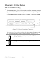
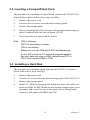
UNO-2176
Pentium M/Celeron M UNO
with 2 X LAN, 6 X COM, 16 x DI/O
User Manual
Copyright
This document is copyrighted, © 2007. All rights are reserved. The original manufacturer reserves the right to make improvements to the products
described in this manual at any time without notice.
No part of this manual may be reproduced, copied, translated or transmitted in any form or by any means without the prior written permission of
the original manufacturer. Information provided in this manual is
intended to be accurate and reliable. However, the original manufacturer
assumes no responsibility for its use, nor for any infringements upon the
rights of third parties that may result from such use.
Acknowledgements
IBM, PC/AT, PS/2 and VGA are trademarks of International Business
Machines Corporation.
Intel® and Pentium® are trademarks of Intel Corporation.
Microsoft Windows and MS-DOS are registered trademarks of Microsoft
Corp.
C&T is a trademark of Chips and Technologies, Inc.
All other product names or trademarks are properties of their respective
owners.
This manual is for UNO-2176.
Part No. 2003217600
1st Edition
Printed in Taiwan
UNO-2176 User Manual
May 2007
ii
Product Warranty
Advantech warrants to you, the original purchaser, that each of its products will be free from defects in materials and workmanship for one year
from the date of purchase.
This warranty does not apply to any products that have been repaired or
altered by persons other than repair personnel authorized by Advantech,
or which have been subject to misuse, abuse, accident or improper installation. Advantech assumes no liability under the terms of this warranty as
a consequence of such events.
Because of Advantech high quality-control standards and rigorous testing, most of our customers never need to use our repair service. If an
Advantech product is defective, it will be repaired or replaced at no
charge during the warranty period. For out-of-warranty repairs, you will
be billed according to the cost of replacement materials, service time and
freight. Please consult your dealer for more details. If you think you have
a defective product, follow these steps:
Step 1. Collect all the information about the problem encountered. (For
example, CPU speed, Advantech products used, other hardware
and software used, etc.) Note anything abnormal and list any onscreen messages you get when the problem occurs.
Step 2. Call your dealer and describe the problem. Please have your manual, product, and any helpful information readily available.
Step 3. If your product is diagnosed as defective, obtain an RMA (return
merchandize authorization) number from your dealer. This
allows us to process your return more quickly.
Step 4. Carefully pack the defective product, a fully completed Repair
and Replacement Order Card and a photocopy proof of purchase
date (such as your sales receipt) in a shippable container. A product returned without proof of the purchase date is not eligible for
warranty service.
Step 5. Write the RMA number visibly on the outside of the package and
ship it prepaid to your dealer.
iii
Declaration of Conformity
CE
This product has passed the CE test for environmental specifications
when shielded cables are used for external wiring. We recommend the use
of shielded cables. This kind of cable is available from Advantech. Please
contact your local supplier for ordering information.
FCC Class A
Note: This equipment has been tested and found to comply with the limits
for a Class A digital device, pursuant to part 15 of the FCC Rules. These
limits are designed to provide reasonable protection against harmful
interference when the equipment is operated in a commercial environment. This equipment generates, uses, and can radiate radio frequency
energy and, if not installed and used in accordance with the instruction
manual, may cause harmful interference to radio communications. Operation of this equipment in a residential area is likely to cause harmful interference in which case the user will be required to correct the interference
at his own expense.
Technical Support and Assistance
Step 1. Visit the Advantech web site at www.advantech.com/support
where you can find the latest information about the product.
Contact your distributor, sales representative, or Advantech's customer
service center for technical support if you need additional assistance.
Please have the following information ready before you call:
- Product name and serial number
- Description of your peripheral attachments
- Description of your software (OS, version, application software, etc.)
- A complete description of the problem
- The exact wording of any error messages
UNO-2176 User Manual
iv
Contents
Chapter
1 Overview ...........................................................2
1.1
1.2
1.3
1.4
Introduction ....................................................................... 2
Hardware Specifications ................................................... 3
Safety Precautions ............................................................. 5
Chassis Dimensions........................................................... 6
Figure 1.1:Chassis Dimensions 1.................................... 6
Figure 1.2:Chassis Dimensions 2.................................... 6
Figure 1.3:Chassis Dimensions 3.................................... 6
Chapter
2 Hardware Functionality ..................................8
2.1
Introduction ....................................................................... 8
Figure 2.1:UNO-2176 Front Panel ................................. 8
Figure 2.2:UNO-2176 Rear Panel .................................. 8
2.2
RS-232 Interface (COM1~COM2) ................................... 8
2.2.1
2.3
2.3.1
2.3.2
2.3.3
2.3.4
2.3.5
2.3.6
2.4
2.5
2.6
2.7
2.8
2.9
Chapter
16PCI954 UARTs with 128-byte Standard .................... 9
RS-422/485 Detection..................................................... 9
Automatic Data Flow Control Function for RS-485 ...... 9
Termination Resistor (J1~J4).......................................... 9
RS-232/422/485 Selection ............................................ 10
Figure 2.3:RS-422/485 Jumper Setting ........................ 10
Figure 2.4:RS-232 Jumper Setting................................ 10
RS-485 Auto Flow & RS-422 Master/Slave Mode ...... 10
LAN: Ethernet Connector .............................................. 11
Power Connector ............................................................. 12
PS/2 Keyboard and Mouse Connector ............................ 12
USB Connector ............................................................... 12
VGA Display Connector ................................................. 12
Battery Backup SRAM.................................................... 13
2.9.1
2.10
IRQ and Address Setting ................................................ 8
RS-232/422/485 Interface (COM3~COM6) ..................... 9
Lithium Battery Specification....................................... 13
Figure 2.5:SRAM Lithium Battery Location................ 13
Reset Button .................................................................... 13
3 Initial Setup.....................................................28
3.1
Chassis Grounding .......................................................... 28
3.2
3.3
3.4
3.5
Inserting a CompactFlash Card ....................................... 29
Installing a Hard Disk ..................................................... 29
Connecting Power ........................................................... 30
BIOS Setup and System Assignments ............................ 30
Figure 3.1:Chassis Grounding Connection................... 28
v
Table of Contents
Appendix A System Settings & Pin Assignments .............32
A.1
A.2
System I/O Address & Interrupt Assignments................ 32
Board Connectors and Jumpers....................................... 34
Figure A.1:Connectors & Jumpers (frontside) ............. 34
Figure A.2:Connectors & Jumpers (backside).............. 34
A.3
A.4
A.5
A.6
A.7
A.8
A.9
RS-232 Standard Serial Port (COM1~COM2) ............... 36
RS-232/422/485 Serial Port ............................................ 37
Ethernet RJ-45 Connector (LAN1~LAN2)..................... 38
Phoenix Power Connector (PWR)................................... 39
PS/2 Keyboard and Mouse Connector ............................ 39
USB Connector (USB1~USB2) ...................................... 40
VGA Display Connector ................................................. 40
Appendix B Programming the Watchdog Timer .............44
UNO-2176 User Manual
vi
CHAPTER
1
2
Overview
This chapter provides an overview of
UNO-2176’s specifications.
Sections include:
• Introduction
• Hardware specification
• Safety precautions
• Chassis dimensions
Chapter 1 Overview
1.1 Introduction
UNO-2176 is an embedded Application Ready Platform (ARP) that can
shorten your development time and offers rich networking interfaces to
fulfill extensive needs in different projects. Advantech’s Universal Network Controller is designed to be a total solution for network enabled
Application Ready Platforms.
Leveraging field-approved and worldwide approved real-time OS technology, Advantech’s UNO-2000 series provides a Windows CE .NET and
Windows XP Embedded ready solution, and supports several standard
networking interfaces, such as Ethernet, Wireless LAN, RS-232/422/485
and so on. Because of its openness, great expansion capability and reliable design (fanless and diskless), the UNO-2000 series are ideal embedded platforms for implementing custom applications for diversified
applications.
UNO-2176 User Manual
2
1.2 Hardware Specifications
• CPU: Pentium M / Celeron M
• Memory: 512MB on board
• Battery-backup RAM: 512 KB Battery-backup RAM
• VGA/Keyboard/Mouse: DB-15 VGA Connector, PS/2 keyboard & mouse
• Serial Ports:
2 x RS-232
2 x Isolated RS-232/422/485 with DB9 connectors
2 x Isolated RS-232/422/485 with 5-pin screw terminal
Automatic RS-485 data flow control
Isolation protection: 2,000 VDC
Surge protection: 2,000 VDC (EFT)
• Serial Speeds:
(COM1,COM2) RS-232: 50 ~ 115.2 kbps,
(COM3-COM6) RS-232: 300 ~ 115.2 kbps
RS-422/485: 300 ~ 921.6 kbps (Max.)
• LAN: Two 10/100 Base-T RJ-45 Ports
• USB interface: Two USB ports, USB UHCI, Rev. 2.0 compliant
• SSD: One internal Type I / Type II CompactFlash card slot
• LEDs: IDE, Alarm for RAM Backup Battery, Programmable LED and
Serial (Tx, RX, COM1~COM4)
• PC/104: PC/104 slot, Supports +5V Power
• HDD: One standard 2.5” HDD
• Digital Inputs:
8-ch wet contact
2,000 VDC isolation
2,000 VDC ESD protection
70 VDC over-voltage protection
±50 VDC input range and 10 kHz speed
Interrupt handling speed: 10 kHz
• Input Voltage:
Logic 0: 0 ~ 3 VDC
Logic 1: 10 ~ 50 VDC
3
Chapter 1
• Input Currents: 10 VDC: 1.7 mA (typical)
12 VDC: 2.1 mA (typical)
24 VDC: 4.4 mA (typical)
48 VDC: 9.0 mA (typical)
50 VDC: 9.4 mA (typical)
• Digital Outputs: 8-ch DO
2,000 VDC Isolation &
200 mA max/channel sink current
Keep output status after system hot reset
5 ~ 40 VDC output range and 10 kHz speed
• Timer/Counter: Counter source: DI1 & DI3
Pulse output: DO2 & DO3
Can be cascaded as one 32-bit counter/timer
Down counting, preset counting value
Timer time base: 100 kHz, 10 kHz, 1 kHz, 100 Hz
• Watchdog Timer: Programmable
• Anti-Shock: 20 G @ Wall mounting, IEC 68 2-27, half sine, 11 ms w/
HDD50 G @ Wall mounting, IEC 68 2-27, half sine, 11 ms w/CF
• Anti-Vibration: 2 Grms w/CF @IEC 68 section 2-64, random, 5 ~ 500 Hz
1 Oct./min, 1 hr/axis. 1 Grms w/ HDD @ IEC 68 section
2-64, random, 5 ~ 500 Hz, 1 Oct./min, 1 hr/axis
• Power Requirement: Min. 48 W (9 ~ 36 VDC) (e.g +24 V @ 2 A) (AT)
• Power Consumption: 24W (Typical)
• Operating Temperature:
-20~65° C (-4~149° F)@ 5 ~ 85% RH (Celeron)
-20~60° C (-4~149° F) @ 5 ~ 85% RH (Pentium Model)
• Storage Temperature: -20~80° C (-4~176° F)
• Relative Humidity: 95% @ 40°C
• Weight: 2.4 kg
• Chassis Size (W × L × H): 255 x 152 x 59 mm (10”× 6.0”× 2.36”)
• Software: Windows XP Embedded, Win2000/XP, Win CE 5.0
• Certification: CE, FCC Class A, UL
UNO-2176 User Manual
4
1.3 Safety Precautions
The following sections tell how to make each connection. In most cases,
you will simply need to connect a standard cable.
Warning!
Always disconnect the power cord from your
chassis whenever you are working on it. Do not
connect while the power is on. A sudden rush of
power can damage sensitive electronic components. Only experienced electronics personnel
should open the chassis.
Caution!
Always ground yourself to remove any static
electric charge before touching UNO-2176. Modern electronic devices are very sensitive to static
electric charges. Use a grounding wrist strap at
all times. Place all electronic components on a
static-dissipative surface or in a static-shielded
bag.
5
Chapter 1
1.4 Chassis Dimensions
Figure 1.1: Chassis Dimensions 1
Figure 1.2: Chassis Dimensions 2
Figure 1.3: Chassis Dimensions 3
UNO-2176 User Manual
6
CHAPTER
2
2
Hardware Functionality
This chapter shows how to setup the
UNO-2176’s hardware functions,
including connecting peripherals, setting switches and indicators.
Sections include:
• Introduction
• RS-232 Interface
• RS-232/422/485 Interface
• LAN / Ethernet Connector
• Power Connector
• PS/2 Mouse and Keyboard Connector
• USB Connector
• VGA Display Connector
• Battery Backup SRAM
• Reset Button
• Onboard Isolated Digital Input
• Onboard Isolated Digital Output
• Onboard Isolated Counter/Timer
Chapter 2 Hardware Functionality
2.1 Introduction
The following two figures show the connectors on UNO-2176. The following sections give you detailed information about function of each
peripheral.
Figure 2.1: UNO-2176 Front Panel
Figure 2.2: UNO-2176 Rear Panel
2.2 RS-232 Interface (COM1~COM2)
The UNO-2176 offers two standard RS-232 serial communication interface ports: COM1 and COM2. Please refer to A.3 for their pin assignments.
2.2.1 IRQ and Address Setting
The IRQ and I/O address range of COM1 and COM2 are listed below:
COM1: 3F8H, IRQ4
COM2: 2F8H, IRQ3
COM3 & COM4 support 9-wire RS-232, RS-422 and RS-485 interfaces.
COM5 & COM6 support 5-wire RS-232, RS-422 and RS-485 interfaces.
UNO-2176 User Manual
8
2.3 RS-232/422/485 Interface (COM3~COM6)
The UNO-2176 offers four RS-232/422/485 serial communication interface ports: COM3 and COM6. COM3 and COM4 support 9-wire RS-232,
RS-422 and RS-485 interfaces. COM5 and COM6 support 5-wire RS232, RS-422 and RS-485 interfaces. Please refer to Appendix A.4 for
their pin assignments. The default setting of COM3 and COM6 are RS422/485.
2.3.1 16PCI954 UARTs with 128-byte Standard
Advantech UNO-2176 comes with Oxford 16PCI964 UARTs containing
128 bytes FIFOs.
2.3.2 RS-422/485 Detection
In RS-422/485 mode, UNO-2176 automatically detects signals to match
RS-422 or RS-485 networks. (No jumper change required)
2.3.3 Automatic Data Flow Control Function for RS-485
In RS-485 mode, UNO-2176 automatically detects the direction of
incoming data and switches its transmission direction accordingly. So no
handshaking signal (e.g. RTS signal) is necessary. This lets you conveniently build an RS-485 network with just two wires. More importantly,
application software previously written for half duplex RS-232 environments can be maintained without modification.
2.3.4 Termination Resistor (J1~J4)
The onboard termination resistor (120 ohm) for COM3/COM6 can be
used for long distance transmission or device matching. (Default Open.)
Pin
Description
A
B
DATA+, DATA-, TX+, TXRX+, RX-
9
Chapter 2
2.3.5 RS-232/422/485 Selection
COM3 and COM4 support 9-wire RS-232, RS-422 and RS-485 interfaces. COM5 and COM6 support 5-wire RS-232, RS-422 and RS-485
interfaces. The system detects RS-422 or RS-485 signals automatically in
RS-422/485 mode. Please refer below table to adjust SW for selecting
serial type of COM3~COM6.
Switch setting for RS-422/485 interface: (Default setting). (SW3~SW6)
Figure 2.3: RS-422/485 Jumper Setting
Switch setting for RS-232 interface: (SW3~SW6)
Figure 2.4: RS-232 Jumper Setting
2.3.6 RS-485 Auto Flow & RS-422 Master/Slave Mode
You can set the “Auto Flow Control” mode of RS-485 or “Master/Slave”
mode of RS-422 by using the SW7 DIP switch for COM3~COM6.
In RS-485, if the switch is set to “Off”, the driver automatically senses
the direction of the data flow and switches the direction of transmission.
No handshaking is necessary.
In RS-422, if DIP switch is set to “On,” the driver is always enabled, and
always in high or low status. Please refer below for the default setting.
UNO-2176 User Manual
10
SW7
Switch
Serial Port
Status
Status
1
COM3
ON
RS-422: Master mode
RS-485: N/A
RS-485: Auto flow control
RS-422: Slave mode
RS-422: Master mode
RS-485: N/A
RS-485: Auto flow control
RS-422: Slave mode
RS-422: Master mode
RS-485: N/A
RS-485: Auto flow control
RS-422: Slave mode
RS-422: Master mode
RS-485: N/A
RS-485: Auto flow control
RS-422: Slave mode
OFF (Default)
2
COM4
ON
OFF (Default)
3
COM5
ON
OFF (Default)
4
COM6
ON
OFF (Default)
2.4 LAN: Ethernet Connector
The UNO-2176 is equipped with a Realtek RTL8139DL Ethernet LAN
controller that is fully compliant with IEEE 802.3u 10/100Base-T
CSMA/CD standards. The Ethernet port provides a standard RJ-45 jack
on board, and LED indicators on the front side to show its Link (Green
LED) and Active (Yellow LED) status.
11
Chapter 2
2.5 Power Connector
The UNO-2176 comes with a Phoenix connector that carries 9~36 VDC
(AT) external power input, and features reversed wiring protection.
Therefore, it will not cause any damage to the system by reversed wiring
of ground line and power line. Please refer to Appendix A.6
2.6 PS/2 Keyboard and Mouse Connector
The UNO-2176 provides a PS/2 keyboard and PS/2 mouse connector. A
6-pin mini-DIN connector is located on the rear panel of the UNO-2176.
The UNO-2176 comes with an adapter to convert from the 6-pin miniDIN connector to two 6-pin mini-DIN connectors for PS/2 keyboard and
PS/2 mouse connection. Please refer to Appendix A.7 for its pin assignments.
2.7 USB Connector
The USB connector is used for connecting any device that conforms to
the USB interface. Many recent digital devices conform to this standard.
The USB interface supports Plug and Play, which enables you to connect
or disconnect a device whenever you want, without turning off the computer.
The UNO-2176 provides two connectors of USB interfaces, which gives
complete Plug & Play and hot swapping for up to 127 external devices.
The USB interface complies with USB EHCI, Rev. 2.0 compliant. The
USB interface can be disabled in the system BIOS setup. Please refer to
Appendix A.8 for its pin assignments.
2.8 VGA Display Connector
The UNO-2176 provides a VGA controller (Intel 855/852 GME, supports
a single 1.5V accelerated graphics port interface) for a high resolution
VGA interface. It supports CRT Mode: 1280 x 1024 @ 32bpp (60Hz),
1024 x 768 @ 32bpp (85Hz); LCD/Simultaneous Modes: 1280 x 1024 @
16bpp(60Hz), 1024 x 768 @16bpp(60Hz) and up to 32 MB shared memory.
UNO-2176 User Manual
12
2.9 Battery Backup SRAM
UNO-2176 provides 512 KB of battery backed SRAM. This ensures that
you have a safe place to store critical data. You can now write software
applications without being concerned that system crashes will erase critical data from the memory.
There is a BTRY LED in the front panel of the UNO-2176, please replace
the lithium battery with a new one if the BTRY LED is activated.
2.9.1 Lithium Battery Specification
• Type: BR2032 (Using CR2032 is NOT recommended)
• Output voltage: 3 VDC
• Location: the backside of UNO-2176 board.
(BH2 is for real time clock, BH1 is for SRAM)
Figure 2.5: SRAM Lithium Battery Location
2.10 Reset Button
Press the "Reset" button to activate the reset function. (SW1)
13
Chapter 2
2.11 Onboard Isolated Digital Input
The UNO-2176 has 8 isolated DI channels designated DI0~DI7.
2.11.1 Pin Assignments
The connector type of UNO-2176 is plug-in screw terminal block that
enables you to connect to field I/O devices directly without additional
accessories. Figure 2.6 and Table 2.1 shows its pin assignment as well as
signal description.
Figure 2.6: Digital Input Connector Pin Assignments
Table 2.1: Digital Input Connector Signal Description
Signal Name
DI <0...7>
COM
Reference
COM
-
Direction
Description
Input
-
Isolated DI signals
DI, DO isolated ground
2.11.2 Isolated Inputs
Each of isolated digital input channels accepts 0 ~ 50 VDC voltage inputs,
and accepts bi-directional input. The voltage range is -3 ~ 3 VDC for logic
0 (low), -50 ~ -10 VDC and 10 ~ 50 VDC for logic 1 (high). It means that
you can apply positive or negative voltage to an isolated input pin (Vin).
All channels share one common pin (COM). Figure 2.7 shows how to connect an external input source to an UNO-2176 isolated input channel.
Please note that DI0 and DI2 may be configured as gate control pins of
Counter 0 and Counter 1; While DI1 and DI3 may be configured as input
pins of Counter 0 and Counter 1. Please refer to section 2.13 for details.
UNO-2176 User Manual
14
Note:
Refer to Appendix A.10 for command of DI
Figure 2.7: Isolated Digital Input Connection
2.11.3 Interrupt Function of the DI Signals
DI0 and DI1 can be used to generate hardware interrupts. Users can setup
the configuration of them by programming the interrupt control register.
The channels are connected to the interrupt circuitry. Users can disable/
enable interrupt function, select trigger type or latch the port data by setting the Interrupt Control Register of the UNO-2176 (refer to section
2.11.5 below). When the interrupt request signals occur, then the software
will service these interrupt requests by ISR (Interrupt Service Routine).
The multiple interrupt sources provide the card with more capability and
flexibility.
2.11.4 IRQ Level
The IRQ level is by default set by the system BIOS. IRQ 7 is reserved for
DI interrupt and counter interrupt.
15
Chapter 2
2.11.5 Interrupt Control Register
Table 2.2: Interrupt Control Register Bit Map
Base Address
202H
7
R/W
6
5
4
3
2
1
0
Interrupt Enable Control/Status Register
DI1EN DI0EN
203H
207H
R/W
R/W
Interrupt Triggering Edge Control/Status Register
DI1TE
DI0TE
DI1F
DI0F
Interrupt Flag/Clear Register
The Interrupt Control Register controls the function and status of each
interrupt signal source. Table 2.2 shows the bit map of the Interrupt Control Register. The register is readable/writeable register. While being written, it is used as a control register; and while being read, it is used as a status register.
DI0EN & DI1EN: DI0 & DI1 Interrupt disable/enable control bit
DI0TE & DI1TE: DI0 & DI1 Interrupt triggering edge control bit
DI0F & DI1F: DI0 & DI1 interrupt flag bit
2.11.6 Interrupt Enable Control Function
Table 2.3: Interrupt Disable/Enable Control
DI0EN & DI1EN
Interrupt Disable/Enable Control
0
Disable
1
Enable
The user can choose to enable or disable the interrupt function by writing
its corresponding value to the interrupt disable/enable control bit in the
interrupt control register, as shown in Table 2.3.
2.11.7 Interrupt Triggering Edge Control
The interrupt can be triggered by a rising edge or a falling edge of the
interrupt signal, as determined by the value in the interrupt triggering edge
control bit in the interrupt control register, as shown in Table 2.4.
UNO-2176 User Manual
16
Table 2.4: Interrupt Triggering Edge Control
DI0TE & DI1TE
Triggering edge of interrupt signal
0
Falling edge trigger
1
Rising edge trigger
2.11.8 Interrupt Flag Bit
The interrupt flag bit is a flag indicating the status of an interrupt. It is a
readable/writable bit. To find the status of the interrupt, you have to read
the bit value. To clear the interrupt, you have to write “1” to this bit. This
bit must first be cleared to service the next coming interrupt.
Table 2.5: Interrupt Flag Bit Values
DI0F & DI1F
Interrupt Status
Read
0
No interrupt
1
Interrupt occur
Write
0
Don’t care
1
Clear interrupt
Note: UNO-2176 provides built-in examples to show how to
deliver digital input functionality. Refer to console mode
examples in
C:\Program Files\Advantech\UNO\UNO_IsaDIO\Examples\Console.
(Please install DI/O driver from the UNO CD to use
these examples)
2.12 Onboard Isolated Digital Output
The UNO-2176 has 8 isolated DO channels designated DO0 ~ DO7.
17
Chapter 2
2.12.1 Pin Assignments
The connector type of UNO-2176 is plug-in screw terminal block that
enables you to connect to field I/O devices directly without additional
accessories. Figure 2.8 and Table 2.6 show its pin assignment as well as
signal description.
Figure 2.8: Digital Output Connector Pin Assignments
Table 2.6: Digital Output Connector Signals
Signal Name
Reference
DO <0...7>
GND
Direction
Description
Output
Isolated DO signals
DI, DO isolated
ground
DO_COM as using
inductance load
GND
-
-
COM
-
-
2.12.2 Power On Configuration
Default configuration after power on or hardware reset is to set all the isolated digital output channels to open status (the current of the load can’t be
sink) so that users need not worry about damaging external devices during
system startup or reset. When the system is hot reset, then the status of isolated digital output channels are selected by jumper JP13. Table 2.7 shows
the configuration of jumper JP13.
Note:
Please refer to Figure A.2 for location of JP13
Table 2.7: Digital Output Power On Configuration
JP13
UNO-2176 User Manual
Power on configuration after hot reset
18
Set to "Open" status
Default setting
Keep last status after hot reset
2.12.3 Isolated Outputs
Each of isolated output channels comes equipped with a Darlington transistor. All output channels share common emitters.
Please note that if an external voltage (5 ~ 40 VDC) is applied to an isolated output channel while it is being used as an output channel, the current will flow from the external voltage source to the UNO-2176. Please
take care that the current through each DO pin not exceed 200 mA. Figure
below shows how to connect an external output load to the UNO-2176 isolated outputs. Please note that DO2 and DO3 may be configured as output
pins of Counter 0 and Counter 1 (refer to section 2.13 for more details)
19
Chapter 2
Note:
Please refer to Appendix A.10 for command of DO
Note:
UNO-2176 provides built-in examples to show how to
deliver digital output functionality. Refer to console
mode examples in C:\Program Files\Advantech\UNO\UNO_IsaDIO\Examples\Console. (Please
install DI/O driver from the UNO CD to use these
examples)
2.13 Onboard Isolated Counter/Timer
The UNO-2176 uses one 82C54 programmable timer/counter chip that
includes three independent 16-bit down counters: counter 0, counter 1 and
counter 2. Counter 0 and counter 1 are for users, and counter 2 is specified
for the system and can’t be used by user. Each counter has clock input, gate
input and pulse output. They can be programmed to count from 2 up to
65535 or cascaded into one 32-bit counter.
The UNO-2176 has two isolated counter input channels designated DI1
and DI3 with two isolated output channels designated DO2 and DO3.
Therefore, you can set each counter of 82C54 as counter function or timer
function.
2.13.1 Counter/Timer Control Register
The Counter/Timer Control Register controls the function and status of
each counter/timer signal source. Table 2.8 shows the bit map of the Counter/Timer Control Register. The register is readable/writable register. While
being written, it is used as a control register; and while being read, it is
used as a status register.
UNO-2176 User Manual
20
Table 2.8: Counter/Timer Control Register Bit Map
Base
Address
7
6
5
4
3
207H
R/W Interrupt Flag/Clear Register
208H
R/W 82C54 Chip Counter0 Register
209H
R/W 82C54 Chip Counter1 Register
20BH
R/W 82C54 Chip Control Register
2
1
0
CTR1F CTR0F
20CH R/W Counter0 Start Control / Output Status Register
CTR0
Out
CTR0
Gate
20DH R/W Counter1 Start Control / Output Status Register
CTR1
Out
20EH
20FH
CTR1
Gate
R/W Counter0 Setting Register
CTR0
IntSet
CTR0 CTR0
OutSet GateSet
CTR0
CLKSet
CTR1
IntSet
CTR1 CTR1
OutSet GateSet
CTR1
CLKSet
R/W Counter1 Setting Register
CTR32 S1
Set
S0
CTR0F/CTR1F: (Counter 0/1) interrupt flag bit
CTR0Gate/CTR1Gate: (Counter 0/1) gate control bit
CTR0Out /CTR1Out: (Counter 0/1) output status bit
CTR0CLKSet /CTR1CLKSet: (Counter 0/1) clock source control bit
CTR0GateSet/CTR1GateSet: (Counter 0/1) gate source control bit
CTR0OutSet/CTR1OutSet: (Counter 0 /1) output destination control bit
CTR0IntSet/CTR1IntSet: (Counter 0/1) interrupt control bit
S0/S1: (Counter 0/1) internal clock control bit
CTR32Set: Cascaded 32-bit counter control bit
21
Chapter 2
2.13.2 Counter 0 Function Block
Figure 2.9: Counter 0 Function Block
2.13.3 Counter 1 Function Block
Figure 2.10: Counter 1 Function Block
2.13.4 32-bit Counter Function Block (CTR32Set=1)
Figure 2.11: 32-bit Counter Function Block
UNO-2176 User Manual
22
2.13.5 Counter Clock Source
There are two clock sources available for the user counters by setting
counter clock control bits - CTR0CLKSet and CTR1CLKSet.
Table 2.9: Counter Clock Source Control Bit
CTR0CLKSet
0
1
0
1
CTR1CLKSet
Internal clock (default)
External clock from digital input 1 (DI1) channel
Internal clock (default)
External clock from digital input 3 (DI3) channel
2.13.6 Counter Internal Clock
There are four frequency options to choose according to applications, and
it’s set by internal clock control bits - S0 and S1.
Table 2.10: Counter Internal Clock Control Bit
S1
S0
Time base
0
0
1
1
0
1
0
1
100 KHz (default)
10 KHz
1 KHz
100 Hz
2.13.7 Counter Gate Source
The gate sources you select determine what kind of gate input signal to
enable your counter/timer when receiving clock input. There are two gate
sources available for the user counters by setting gate source control bits CTR0GateSet and CTR1GateSet.
Table 2.11: Counter Gate Source Control Bit
CTR0GateSet
CTR1GateSet
0
Gate source from “CTR0Gate” control bit (Default)
1
Gate source from digital input 0 (DI0) channel
0
Gate source from “CTR1Gate” control bit (Default)
1
Gate source from digital input 2 (DI2) channel
2.13.8 Counter Output Destination
You can choose the output destination of counter 0 and counter 1 by setting
“Output Destination control bits”- CTR0OutSet and CTR1OutSet.
Table 2.12: Counter Output Destination Control Bit
CTR0OutSet
CTR1OutSet
0 Output destination to “CTR0Out” status bit (Default)
1 Output destination to “CTR0Out” status bit and digital output
2 (DO2) channel
0 Output destination to “CTR1Out” status bit. (Default)
1 Output destination to “CTR1Out” status bit and digital output
3 (DO3) channel
23
Chapter 2
2.13.9 Counter Interrupt Flag
The interrupt flag bit is a flag indicating the status of an interrupt. It is a
readable/writable bit. To find the status of the interrupt, you have to read
the bit value; to clear the interrupt, you have to write “1” to this bit. This bit
must first be cleared to service the next coming interrupt. Besides, you can
choose if counter 0 or counter 1 generate interrupt signal by configuring
“CTR0IntSet” and “CTR1IntSet” control bit.
Table 2.13: Counter Interrupt Flag Control Bit
CTR0F, CTR1F
Read
Write
Counter Interrupt Status
0
No interrupt
1
Interrupt occur
0
Don’t care
1
Clear interrupt
CTR0IntSet, CTR1IntSet
Counter Interrupt Control
0
Disable (Default)
1
Enable
2.13.10 Cascaded 32-bit Counter
You can also cascade counter 0 and counter 1 together as one 32-bit counter/timer, and it’s configured by control bit - CTR32Set.
Table 2.14: 32-bit Counter Control Bit
0
Disable (Default)
1
Cascade counter 0 and counter 1 into one 32-bit counter
Note:
UNO-2176 provides built-in examples to show how
to deliver counter functionality. Refer to console
mode examples in C:\Program Files\Advantech\UNO\UNO_IsaDIO\Examples\Console. (Please
install DI/O driver from the UNO CD to use these
examples)
UNO-2176 User Manual
24
2.14 LED and Buzzer for System Diagnosis
In a “headless application” (an application without a monitor display), it is
always difficult to know the system status. Another PC may be needed to
monitor a headless device's status via RS-232 or Ethernet. In order to
solve this problem, UNO-2176 offers a programmable LED indicator and
buzzer. They can be programmed to show a systems status by LED indicator flickering and buzzer alarm.
Table 2.15: LED & Buzzer Control Register
210H
R/W
DIAG LED Register
LEDS1 LEDS0 LEDEn
211H
R/W
Buzzer Register
SPKS1
LEDEn:
SPKS0
SPKEn
=0, DIAG LED disable
=1, DIAG LED enable
LEDS0 and LEDS1: LED flickering speed setting bit (refer to Table 2.16)
SPKEn:
=0, Speaker disable
=1, Speaker enable
SPKS0 & SPKS1: Buzzer alarming setting bit (refer to Table 2.17)
Note: UNO-2176 provides built-in examples to show how to
configure DIAG LED and Buzzer. Refer to console
mode examples in C:\Program Files\Advantech\UNO\UNO_IsaDIO\Examples\Console.
(Please install DI/O driver from the UNO CD to use
these examples)
25
Chapter 2
Table 2.16: Programmable LED Control Bit
LEDS1
LEDS0
Light on
0
0
Fast flicker
0
1
Normal flicker
1
0
Short flicker
1
1
Table 2.17: Programmable Buzzer Control Bit
Beep on
SPKS1
SPKS0
0
0
Short beep
0
1
Normal beep
1
0
Long beep
1
1
PS/2 Keyboard and Mouse Connector
The UNO-2176 provides a PS/2 keyboard and PS/2 mouse connector. A 6pin mini-DIN connector is located on the front panel of the UNO-2176.
UNO-2176 comes with an adapter in the accessory package (see section
1.5) to convert from the 6-pin mini-DIN connector to two 6-pin mini-DIN
connectors for PS/2 keyboard and PS/2 mouse connection. Please refer to
Appendix A.7 for its pin assignments.
UNO-2176 User Manual
26
CHAPTER
3
2
Initial Setup
This chapter introduces how to initialize the UNO-2176.
Sections include:
• Chassis Grounding
• Inserting a CompactFlash Card
• Installing a Hard Disk
• Connecting Power
• BIOS Setup and System Assignments
Chapter 3 Initial Setup
3.1 Chassis Grounding
The aluminum made UNO-2176 provides good EMI protection and a stable grounding base. There is an easy-to-connect chassis grounding point
for you to use.
Please connect chassis ground of UNO-2176 with "EARTH" as ground.
Figure 3.1: Chassis Grounding Connection
You can select if you wish to combine the chassis grounding point with
the system grounding by using an onboard jumper selection. (JP1)
Open - Separates system power ground and chassis
ground. (default)
Closed - Connects system power ground and chassis
ground.
UNO-2176 User Manual
28
3.2 Inserting a CompactFlash Card
The procedure for installing a CompactFlash card into the UNO-2176 is
detailed below, please follow these steps carefully.
1.
Remove the power cord.
2.
Unscrew the six screws from the down storage panel.
3.
Remove the storage panel.
4.
Plug a CompactFlash card with your OS and application program
into a CompactFlash card slot on board. (CN10)
5.
Screw back the rear panel with six screws
Note
CN8 is Primary
CN10 is secondary's master
CN9 is secondary
Please do not use CN9 and CN10 simultaneously.
If your OS is build in CF card and program,application and data are save in HDD, please install CF in
CN10 and connect HDD in CN8.
3.3 Installing a Hard Disk
The procedure for installing a hard disk into the UNO-2176 is below.
Please follow these steps carefully.
1.
Remove the power cord.
2.
Unscrew six screws from the down storage panel of the UNO-2176.
3.
Remove the storage panel.
4.
Install 2.5" HDD on storage panel and please notice the cable connector on HDD for IDE should be near bottom triangle sign of storage panel, and screw 4 screws on the back side of storage panel
connector IDE cable with HDD and CN8
29
Chapter 3
5.
Note:
Screw back the down storage panel with 6 screws
CN8 is Primary
CN10 is secondary's master
CN9 is secondary
Please do not use CN9 and CN10 simultaneously.
If your OS is build in CF card and program,application and data are save in HDD, please install CF in
CN10 and connect HDD in CN8.
3.4 Connecting Power
Connect the UNO-2176 to a 9~36 VDC power source. The power source
can either be from a power adapter or an in-house power source.
3.5 BIOS Setup and System Assignments
UNO-2176 adopts Advantech’s SOM-4486/4481 CPU module. Further
information about the SOM-4486/4481 CPU module, can be found in
SOM-4486/4481’s user’s manual. You can find this manual on the UNO2176’s driver and utility CD-ROM.
Please note that you can try to “LOAD BIOS DEFAULTS” from the
BIOS Setup manual if the UNO-2176 does not work properly.
UNO-2176 User Manual
30
Appendix
A
System Settings and
Pin Assignments
Appendix A System Settings & Pin
Assignments
A.1 System I/O Address & Interrupt Assignments
Table A.1: UNO-2176 System I/O Ports
Address Range Device
000-01F
DMA controller (slave)
020-03F
Interrupt controller 1, (master)
040-05F
8254 timer/counter
060-06F
8042 (keyboard controller)
070-07F
Real-time clock, non-maskable interrupt (NMI)mask
080-09F
DMA page register,
0A0-0BF
Interrupt controller 2 (slave)
0C0-0DF
DMA controller (master)
0F0
Clear math co-processor
0F1
Reset math co-processor
0F8-0FF
Math co-processor
1D0
Vector address; for COM port share IRQ
1E0
Battery backup resource
11E
Battery backup resource
1F0-1F8
1st fixed disk
200-218
Digital inputs, outputs and counter
278-27F
Reserved
2F8-2FF
Serial port 2
380-38F
SDLC, bisynchronous 2
3A0-3AF
Bisynchronous 1
3B0-3BF
Monochrome display
3C0-3CF
Reserved
3D0-3DF
Color/graphics monitor adapter
3F0-3F7
Diskette controller
3F8-3FF
Serial port 1
DC000-DFFFF
Battery backup resource
UNO-2176 User Manual
32
Table A.2: UNO-2176 Interrupt Assignment
Interrupt No.
Interrupt Source
NMI
Parity error detected
IRQ 0
Interval timer
IRQ 1
Keyboard
IRQ 2
Interrupt from controller 2 (cascade)
IRQ 3
COM2
IRQ 4
COM1
IRQ 6
Diskette controller (FDC)
IRQ 7
Digital inputs, outputs and counter
IRQ 8
Real-time clock
IRQ 11
Reserved for watchdog timer
IRQ 12
PS/2 mouse
IRQ 13
INT from co-processor
IRQ 14
Primary IDE
IRQ 15
Secondary IDE for CompactFlash
33
Appendix A
A.2 Board Connectors and Jumpers
There are several connectors and jumpers on the UNO-2176
board. The following sections tell you how to configure the
UNO-2176 hardware setting. Figure A-1 and Figure A-2
show the locations of UNO-2176’s connectors and jumpers.
Figure A.1: Connectors & Jumpers (frontside)
Figure A.2: Connectors & Jumpers (backside)
UNO-2176 User Manual
34
Table A.3: UNO-2176 Connectors & Jumpers
Label
Function
CN1
Phoenix power connector
CN2
Ethernet port 2
CN3
COM1 RS-232 serial port
CN4
COM2 RS-232 serial port
CN5
Ethernet port 1
CN6
USB connector
CN7
PS/2 keyboard and mouse connector
CN8
Primary IDE connector
CN9
Secondary IDE connector
CN10
Secondary's master IDE connector
CN11
VGA DB15 display connector
CN12
PC/104 slot
CN13
COM3 RS-232/422/485 serial port
CN14
COM4 RS-232/422/485 serial port
JP1
System grounding jumper
JP13
Digital output status seeting
SW1
Reset button
SW3
COM3 RS-232/422/485 selection
SW4
COM4 RS-232/422/485 selection
SW5
COM5 RS-232/422/485 selection
SW6
COM6 RS-232/422/485 selection
SW7
COM3/COM4/COM5/COM6 RS-422 master/slave selection
J1
Terminator resistor (120 ohm) for COM3 (RS-422/485)
J2
Terminator resistor (120 ohm) for COM4 (RS-422/485)
J3
Terminator resistor (120 ohm) for COM5 (RS-422/485)
J4
Terminator resistor (120 ohm) for COM6 (RS-422/485)
BH1
Battery for SRAM
BH2
Battery for RTC
35
Appendix A
A.3 RS-232 Standard Serial Port (COM1~COM2)
Table A.4: RS-232 Standard Serial Port Pin Assigns
Pin
RS-232 Signal Name
1
DCD
2
RxD
3
TxD
4
DTR
5
GND
6
DSR
7
RTS
8
CTS
9
RI
UNO-2176 User Manual
36
A.4 RS-232/422/485 Serial Port
Table A.5: RS-232/422/485 Serial Ports COM3~4
Pin
RS-232
RS-422
RS-485
1
DCD
Tx-
DATA-
2
RxD
Tx+
DATA+
3
TxD
Rx+
NC
4
DTR
Rx-
NC
5
GND
GND
GND
6
DSR
NC
NC
7
RTS
NC
NC
8
CTS
NC
NC
9
RI
NC
NC
37
Appendix A
Table A.6: RS-232/422/485 Serial Ports (COM5~6)
Pins
RS-232
RS-422
RS-485
1
RxD
Tx+
Data+
2
TxD
Tx-
Data-
3
RTS
Rx+
-
4
CTS
Rx-
-
5
GND
GND
GND
A.5 Ethernet RJ-45 Connector (LAN1~LAN2)
Table A.7: Ethernet RJ-45 Connector Pin Assignments
Pin
10/100Base-T Signal Name
1
XMT+
2
XMT-
3
RCV+
4
NC
5
NC
6
RCV-
7
NC
8
NC
UNO-2176 User Manual
38
A.6 Phoenix Power Connector (PWR)
Table A.8: Power Connector Pin Assignments
Pin
Signal Name
1
+9~36VDC
2
GND
A.7 PS/2 Keyboard and Mouse Connector
Table A.9: Keyboard & Mouse Connector Pin Assigns
Pin
Signal Name
1
KB DATA
2
MS DATA
3
GND
4
VCC
5
KB Clock
6
MS Clock
39
Appendix A
A.8 USB Connector (USB1~USB2)
Table A.10: USB Connector Pin Assignments
Pin
Signal Name
Cable Color
1
VCC
Red
2
DATA-
White
3
DATA+
Green
4
GND
Black
A.9 VGA Display Connector
5
1
10
6
15
11
Table A.11: VGA Adaptor Cable Pin Assignments
Pin
Signal Name
1
Red
2
Green
3
Blue
4
NC
5
GND
6
GND
7
GND
8
GND
9
NC
10
GND
11
NC
12
NC
13
H-SYNC
14
V-SYNC
15
NC
UNO-2176 User Manual
40
A.10 UNO-2176 Control Register
Table A.12: UNO-2176 Control Register
Base
Address
200H
R
7
6
5
4
3
2
201H
R/W
202H
R/W
Isolated Digital Input Status Register
DI7
DI6
DI5
DI4
DI3
DI2
Isolated Digital Output Control/Status Register
DO7
DO6
DO5
DO4
DO3
DO2
Interrupt Enable Control/Status Register
203H
R/W
Interrupt Triggering Edge Control/Status Register
207H
R/W
Interrupt Flag/Clear Register
208H
R/W
82C54 Chip Counter0 Register*
209H
R/W
82C54 Chip Counter1 Register*
20BH
R/W
82C54 Chip Control Register*
20CH
R/W
Counter0 Start Control / Output Status Register
CTR0
Out
Counter1 Start Control / Output Status Register
CTR1
Out
Counter0 Setting Register
CTR0 CTR0
IntSet OutSet
Counter1 Setting Register
CTR
S1
S0
CTR1 CTR1
32Set
IntSet OutSet
DIAG LED Control Register
LEDS1
Buzzer Control Register
SPKS1
Power Register
PWR
1
0
DI1
DI0
DO1
DO0
DI1EN
DI0EN
DI1TE
DI0TE
CTR1F CTR0F DI1F
20DH
20EH
20FH
R/W
R/W
R/W
210H
R/W
211H
R/W
218H
R
DI0F
CTR0
Gate
CTR1
Gate
CTR0
CTR0
GateSet CLKSet
CTR1
CTR1
GateSet CLKSet
LEDS0
LEDEn
SPKS0
SPKEn
P2
P1
* Refer to 82c54 manual
41
Appendix A
UNO-2176 User Manual
42
Appendix
Programming the
Watchdog Timer
B
Appendix B Programming the Watchdog
Timer
Below are samples of code for controlling the Watchdog Timer function.
----------------------------------------------------------------------------------Enter the extended function mode, interruptible double-write |
----------------------------------------------------------------------------------MOV DX,2EH
MOV AL,87H OUT DX,AL OUT DX,AL
----------------------------------------------------------------------------Configured logical device 8, configuration register CRF6 |
----------------------------------------------------------------------------MOV DX,2EH
MOV AL,2BH OUT DX,AL MOV DX,2FH IN AL,DX
AND AL.OEFH;Setbit 4=0 Pin 89=WDTO OUT DX,AL
MOV DX,2EH
MOV AL,07H; point to Logical Device Number Reg. OUT DX,AL
MOV DX,2FH
MOV AL,08H; select logical device 8
OUT DX,AL; MOV DX,2EH
MOV AL,30H;Set watch dog activate or inactivate
OUT DX,AL MOV DX,2FH
MOV AL,01H; 01:activate 00:inactivate
OUT DX,AL; MOV DX,2EH
MOV AL,F5H; Setting counter unit is second
OUT DX,AL MOV DX,2FH MOV AL,00H OUT DX,AL; MOV
DX,2EH MOV AL,F6H OUT DX,AL MOV DX,2FH
MOV AL,05H; Set 5 seconds
OUT DX,AL
;-----------------------------------------; Exit extended function mode |
;-----------------------------------------MOV DX,2EH
MOV AL,AAH OUT DX,AL
UNO-2176 User Manual
44