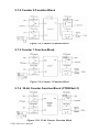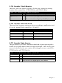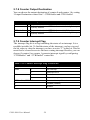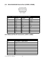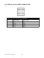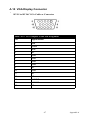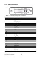
1
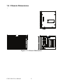
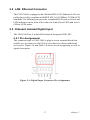
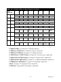
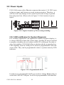
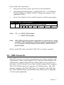
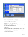
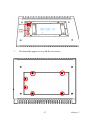
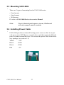
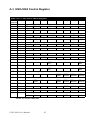
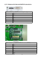
UNO-3084 Core 2 Duo Embedded Automation Computer with One PCI Express and Three PCI Slot Extensions User Manual i Copyright Notice The documentation and the software included with this product are copyrighted 2010 by Advantech Co., Ltd. All rights are reserved. Advantech Co., Ltd. reserves the right to make improvements in the products described in this manual at any time without notice. No part of this manual may be reproduced, copied, translated or transmitted in any form or by any means without the prior written permission of Advantech Co., Ltd. Information provided in this manual is intended to be accurate and reliable. However, Advantech Co., Ltd. assumes no responsibility for its use, nor for any infringements of the rights of third parties, which may result from its use. Acknowledgements IBM, PC/AT, PS/2 and VGA are trademarks of International Business Machines Corporation. Intel® and Pentium® are trademarks of Intel Corporation. Microsoft Windows and MS-DOS are registered trademarks of Microsoft Corp. C&T is a trademark of Chips and Technologies, Inc. All other product names or trademarks are properties of their respective owners. Part No. 2003308400 1st Edition Printed in Taiwan February 2010 UNO-3084 User Manual ii Product Warranty (2 years) Advantech warrants to you, the original purchaser, that each of its products will be free from defects in materials and workmanship for two years from the date of purchase. This warranty does not apply to any products which have been repaired or altered by persons other than repair personnel authorized by Advantech, or which have been subject to misuse, abuse, accident or improper installation. Advantech assumes no liability under the terms of this warranty as a consequence of such events. Because of Advantech’s high quality-control standards and rigorous testing, most of our customers never need to use our repair service. If an Advantech product is defective, it will be repaired or replaced at no charge during the warranty period. For out-of-warranty repairs, you will be billed according to the cost of replacement materials, service time and freight. Please consult your dealer for more details. If you think you have a defective product, follow these steps: 1. Collect all the information about the problem encountered. (For example, CPU speed, Advantech products used, other hardware and software used, etc.) Note anything abnormal and list any onscreen messages you get when the problem occurs. 2. Call your dealer and describe the problem. Please have your manual, product, and any helpful information readily available. 3. If your product is diagnosed as defective, obtain an RMA (return merchandize authorization) number from your dealer. This allows us to process your return more quickly. 4. Carefully pack the defective product, a fully-completed Repair and Replacement Order Card and a photocopy proof of purchase date (such as your sales receipt) in a shippable container. A product returned without proof of the purchase date is not eligible for warranty service. 5. Write the RMA number visibly on the outside of the package and ship it prepaid to your dealer. iii CE This product has passed the CE test for environmental specifications when shielded cables are used for external wiring. We recommend the use of shielded cables. This kind of cable is available from Advantech. FCC Class A This equipment has been tested and found to comply with the limits for a Class A digital device, pursuant to part 15 of the FCC Rules. These limits are designed to provide reasonable protection against harmful interference when the equipment is operated in a commercial environment. This equipment generates, uses, and can radiate radio frequency energy and, if not installed and used in accordance with the manual, may cause harmful interference to radio communications. Operation of this equipment in a residential area is likely to cause harmful interference in which case the user will be required to correct the interference at his own expense. Technical Support and Assistance Step 1. Visit the Advantech web site at www.advantech.com/support where you can find the latest information about the product. Step 2. Contact your distributor or Advantech's customer service center if you need additional assistance. Have the following info ready: - Product name and serial number - Description of your software (OS, version, software, etc.) - A complete description of the problem - The exact wording of any error messages UNO-3084 User Manual iv Safety Instructions 1. Read these safety instructions carefully. 2. Keep this User's Manual for later reference. 3. Disconnect this equipment from any AC outlet before cleaning. Use a damp cloth. Do not use liquid or spray detergents for cleaning. 4. For plug-in equipment, the power outlet socket must be located near the equipment and must be easily accessible. 5. Keep this equipment away from humidity. 6. Put this equipment on a reliable surface during installation. Dropping it or letting it fall may cause damage. 7. The openings on the enclosure are for air convection. Protect the equipment from overheating. DO NOT COVER THE OPENINGS. 8. Make sure the voltage of the power source is correct before connecting the equipment to the power outlet. 9. Position the power cord so that people cannot step on it. Do not place anything over the power cord. 10. All cautions and warnings on the equipment should be noted. 11. If the equipment is not used for a long time, disconnect it from the power source to avoid damage by transient overvoltage. 12. Never pour any liquid into an opening. This may cause fire or electrical shock. 13. Never open the equipment. For safety reasons, the equipment should be opened only by qualified service personnel. 14. If one of the following situations arises, get the equipment checked by service personnel: a. The power cord or plug is damaged. b. Liquid has penetrated into the equipment. c. The equipment has been exposed to moisture. d. The equipment does not work well, or you cannot get it to work according to the user's manual. e. The equipment has been dropped and damaged. f. The equipment has obvious signs of breakage. 15. DO NOT LEAVE THIS EQUIPMENT IN AN ENVIRONMENT WHERE THE STORAGE TEMPERATURE MAY GO BELOW v -10° C (14° F) OR ABOVE 60° C (140° F). THIS COULD DAMAGE THE EQUIPMENT. THE EQUIPMENT SHOULD BE IN A CONTROLLED ENVIRONMENT. 16. CAUTION: DANGER OF EXPLOSION IF BATTERY IS INCORRECTLY REPLACED. REPLACE ONLY WITH THE SAME OR EQUIVALENT TYPE RECOMMENDED BY THE MANUFACTURER, DISCARD USED BATTERIES ACCORDING TO THE MANUFACTURER'S INSTRUCTIONS. The sound pressure level at the operator's position according to IEC 7041:1982 is no more than 70 dB (A). DISCLAIMER: This set of instructions is given according to IEC 704-1. Advantech disclaims all responsibility for the accuracy of any statements contained herein. Safety Precaution - Static Electricity Follow these simple precautions to protect yourself from harm and the products from damage. 1. To avoid electrical shock, always disconnect the power from your PC chassis before you work on it. Don't touch any components on the CPU card or other cards while the PC is on. 2. Disconnect power before making any configuration changes. The sudden rush of power as you connect a jumper or install a card may damage sensitive electronic components. UNO-3084 User Manual vi Contents Chapter Chapter 1 Overview .......................................................... 2 1.1 1.2 1.3 1.4 Introduction ....................................................................... 2 Hardware Specifications ................................................... 2 Safety Precautions ............................................................. 5 Chassis Dimensions........................................................... 6 1.5 Packing List....................................................................... 7 Figure 1.1:Chassis Dimensions ...................................... 6 2 Hardware Functionality ............................... 10 2.1 Introduction ..................................................................... 10 2.2 RS-232/422/485 Interface (COM1~COM2) .................. 11 Figure 2.1:Front Panel of UNO-3084 .......................... 10 2.2.1 2.2.2 2.2.3 2.2.4 2.2.5 2.2.6 2.3 2.4 2.5 Optional RS-232 Interfaces (COM3~COM4)................. 15 LAN: Ethernet Connector ............................................... 17 Onboard Isolated Digital Input........................................ 17 2.5.1 2.5.2 2.5.3 2.5.4 2.5.5 2.5.6 2.5.7 2.5.8 2.6 16C950 UARTs with 16-byte FIFO Standard ............. 11 RS-422/485 Jumperless Detection ............................... 11 Automatic Data Flow Control Function for RS-485 ... 11 RS-232/422/485 Selection ........................................... 11 Figure 2.2:RS-422/485 Jumper Setting ....................... 12 Figure 2.3:RS-232 Jumper Setting ............................... 12 Terminal Resistor Setup for RS-422/485 ..................... 13 Table 2.1:Terminal Resistor Settings ........................... 13 RS-485 Auto Flow/RS-422 Master/Slave Selection .... 14 Pin Assignments .......................................................... 17 Figure 2.4:Digital Input Connector Pin Assignments .. 17 Isolated Inputs .............................................................. 18 Figure 2.5:Digital Input Wet Contact Diagram ........... 18 Interrupt Function of the DI Signals ............................ 18 IRQ Level .................................................................... 19 Interrupt Control Register ............................................ 19 Table 2.2:Interrupt Control Register Bit Map ............. 19 Interrupt Enable Control Function ............................... 19 Table 2.3:Interrupt Disable/Enable Control ................. 19 Interrupt Triggering Edge Control ............................... 20 Table 2.4:Interrupt Triggering Edge Control ............... 20 Interrupt Flag Bit ......................................................... 20 Table 2.5:Interrupt Flag Bit Values ............................. 20 Onboard Isolated Digital Output ..................................... 21 2.6.1 2.6.2 Pin Assignments .......................................................... 21 Figure 2.6:Digital Output Connector Pin Assignments 21 Table 2.6:Digital Output Connector Signals ................ 21 Power On Configuration .............................................. 22 Figure 2.7:Location of CN27 ....................................... 22 vii Table of Contents 2.6.3 2.7 2.8 Onboard Isolated Counter/Timer .................................... 24 2.7.1 Counter/Timer Control Register .................................. 24 Table 2.8:Counter/Timer Control Register Bit Map .... 25 2.7.2 Counter 0 Function Block ............................................ 26 Figure 2.8:Counter 0 Function Block .......................... 26 2.7.3 Counter 1 Function Block ............................................ 26 Figure 2.9:Counter 1 Function Block .......................... 26 2.7.4 32-bit Counter Function Block (CTR32Set=1) .......... 26 Figure 2.10:32-bit Counter Function Block ................. 26 2.7.5 Counter Clock Source .................................................. 27 Table 2.9:Counter Clock Source Control Bit ............... 27 2.7.6 Counter Internal Clock ................................................. 27 Table 2.10:Counter Internal Clock Control Bit ........... 27 2.7.7 Counter Gate Source .................................................... 27 Table 2.11:Counter Gate Source Control Bit ............... 27 2.7.8 Counter Output Destination ......................................... 28 Table 2.12:Counter Output Destination Control Bit .... 28 2.7.9 Counter Interrupt Flag ................................................. 28 Table 2.13:Counter Interrupt Flag Control Bit ............ 28 2.7.10 Cascaded 32-bit Counter .............................................. 29 Table 2.14:32-bit Counter Control Bit ......................... 29 Power Inputs.................................................................... 30 2.8.1 2.9 2.10 2.11 Chapter Table 2.7:Digital Output Power On Configuration ..... 22 Isolated Outputs ........................................................... 23 Figure 2.11:Figure Location of Power and grounding 30 LED and Buzzer for System Diagnosis ....................... 30 Figure 2.12:Programmable LED .................................. 30 Table 2.15:LED Control Register ................................ 31 USB Connector .............................................................. 31 DVI-I Display Connector ................................................ 32 2.10.1 VGA Support and Hotkey ............................................ 32 2.10.2 Multiple Video Output Option ..................................... 33 Battery Backup SRAM.................................................... 35 Figure 2.13:LED Location for Battery Backup ........... 35 2.11.1 Lithium Battery Specification ...................................... 35 Figure 2.14:Lithium Battery for SRAM ...................... 35 2.12 2.13 Reset Button .................................................................... 36 Power Button................................................................... 36 2.14 2.15 2.16 Audio............................................................................... 36 IEEE1394 ........................................................................ 37 SATA Hard Drive RAID Support................................... 37 Figure 2.15:Hardware AT mode Jumper Location ...... 36 3 Initial Setup.................................................... 44 3.1 3.2 3.3 3.4 3.5 Inserting a CompactFlash Card ....................................... 44 Connecting Power ........................................................... 44 Installing a Hard Disk ..................................................... 45 Installing a PCI-bus Card ................................................ 48 Mounting UNO-3084 ...................................................... 52 UNO-3084 User Manual viii 3.6 3.7 3.8 Installing Power Cable .................................................... 52 BIOS Setup and System Assignments ............................ 53 Rubber Foot Installation.................................................. 54 Appendix A System Settings and Pin Assignments ......... 56 A.1 System I/O Address and Interrupt Assignments ...... 56 A.2 Board Connectors and Jumpers....................................... 59 A.3 UNO-3084 Control Register ........................................... 62 A.4 RS-232 Standard Serial Port (COM3~COM4) ............... 63 A.5 RS-232/422/485 Serial Port (COM1~COM2) ............... 64 A.6 Ethernet RJ-45 Connector (LAN1~LAN2)..................... 64 A.8 PS/2 Keyboard and Mouse Connector ............................ 65 A.9 USB Connector (USB1~USB4 & CN7) ......................... 66 A.10 VGA Display Connector ................................................. 67 Table A.1:UNO-3084 System I/O Port ........................ 56 Table A.2:UNO-3084 Interrupt Assignments .............. 58 Figure A.1:Backplane Connector & Jumpers .............. 59 Figure A.2:Mainboard Connector & Jumpers (Front) . 59 Table A.3:Connector and Jumper Descriptions ........... 60 Table A.4:Connector and Jumper Descriptions ........... 61 Table A.5:UNO-3084 Control Register ....................... 62 Table A.6:RS-232 Serial Port Pin Assigns .................. 63 Table A.7:RS-232/422/485 Serial Port Pin Assigns .... 64 Table A.8:Ethernet RJ-45 Connector Pin Assigns ....... 64 Table A.10:Keyboard & Mouse Connector Pins ......... 65 Table A.11:USB Connector Pin Assignments ............. 66 Table A.12:VGA Adaptor Cable Pin Assignmen ........ 67 Appendix B Programming the Watchdog Timer ............ 74 ix Table of Contents UNO-3084 User Manual x CHAPTER 1 Overview This chapter provides an overview of UNO-3084 specifications. Sections include: • Introduction • Hardware specification • Safety precautions • Chassis dimensions Chapter 1 Overview 1.1 Introduction Advantech's UNO-3082/3084 are high performance Core 2 Duo Fanless Box PCs with up to four expansion slots and PCI express or PCI support. The Gigabit LAN on the UNO-3082/3084 supports Teaming function with fault tolerance, link aggregation, and load balance features. It also equipped two IEEE 1394b bilingual interfaces which allow users to connect their own devices for machine vision or other digital video application. Critical data can be saved in UNO-3082/3084 on the battery backup SRAM. There are also two built in hard drive bays with RAID 0/1 support. It's an ideal platform for sophisticated control and logging in rugged environments. 1.2 Hardware Specifications • CPU: Intel Core 2 Duo Processor L7500 (4M Cache, 1.60 GHz, 800 MHz FSB) • System Memory: Built-in 2GB DDR2 RAM (2 x 200-pin SODIMM sockets, supports up to 4GB DDR RAM) • Battery Backup RAM: 512 KB • Chipset: Intel GME965 Express Chipset GMCH / Intel 82801HEM I/O Controller Hub (ICH8EM) 800 MHz FSB • BIOS: Award 4 Mbit Flash BIOS, supports Boot-on-LAN function • Display: Two DVI-I port, provide Dual DVI-D independent, or DVI-D + Dual VGA cloned displays • Audio: AC 97, Line Out • Clock: Battery-backup RTC for time and date • Serial Ports: 2 x RS-232/422/485 with DB-9 connector and Automatic RS-485 data flow control • RS-232 Speed: 300 bps ~ 115.2 kbps • RS-422/485 Speed: 300 bps ~ 921.6 kbps (Optional cable Serial Ports: 2xRS-232, 50~115.2kbps) • LAN: Two Intel 82574L 10/100/1000 Base-T RJ-45 ports with wake on LAN and teaming function support UNO-3084 User Manual 2 • USB Interface: External:Four USB ports, USB EHCI, Rev. 2.0 compliant Internal: One USB port, USB EHCI, Rev. 2.0 compliant (Optional cable wiring: 2 x USB ports, USB EHCI, Rev 2.0 compliant) • IEEE 1394 Interface: 2 x IEEE 1394 type B with Bilingual connectors • Compact Flash Slots: Two type I/II CompactFlash Slots, One internal and one external • HDD: SATA HDD extension kit for two standard 2.5" HDDs RAID 0/1 function support One external eSATA device (Does not support hot swap) • LEDs: Power, Standby, HDD, Alarm for battery backup, 4 COM ports Tx /Rx, LAN (Active, Status) (Optional: 4x Programmable LED while COM ports Tx/Rx disable) • PCI Express & PCI-bus Slot Power: 12 V @ 3 A -12 V @ 0.8 A 5V@6A 3.3 V @ 6 A 3.3 VSB @ 1.5A Note: Total power total combined power consumption on the PCIe/PCI slots should be less than 40W • 4-ch Isolated Digital Input (Wet Contact, DI0~DI3) 1,500 VDC isolation 1,500 VDC ESD protections 50~70 VDC over-voltage protection 50 VDC input range and 3 kHz speed Input Voltage Range: Dry Contact: Logic level 0: open Logic level 1: close to GND Wet Contact: Logic level 0: -3V ~ +3V Logic level 1: +10 ~ 50 V, -10 ~ -50V • 4-ch Isolated Digital Output (DO0~DO3) - 1,500 VDC isolation and 200 mA max / channel sink current - 2 options after hot reset: Reset all digital output or keep last status - 5~ 40 VDC output range to open collector and 3 kHz speed 3 Chapter 1 • Two 16-bit Counters/Timers: Counter source: DI1 & DI3, Pulse output: DO2 & DO3 Can be cascaded as one 32-bit counter/timer Down counting, preset counting value Interrupt handling, speed: 40 kHz Internal timer time base: 100 kHz, 10 kHz, 1 kHz, 100 Hz • Anti-Shock: 20 G @ Wall mounting, IEC 68 section 2-27, half sine, 11 ms w/HDD 50 G @ Wall mounting, IEC 68 section 2-27, half sine, 11 ms w/CF • Anti-Vibration: 2 Grms w/CF@IEC 68 sec. 2-64, random, 5~500Hz, 1 Oct./min,1hr axis 1 Grms w/HDD@IEC 68 sec. 2-64, random, 5~500Hz, 1 Oct./min, 1hr axis • Power Supply: 9 ~ 36 VDC • Operating Temperature: -10 ~ 55 C (14 ~ 131 F) Note: The temperature inside the chassis may be 5 to 10 C higher than the ambient temperature. To ensure stable performance, please make sure the operating temperature of the installed PCI add-on card is higher than 60 C. • Relative Humidity: 5~95% @ 40 C (non-condensing) • Power Consumption: 40 W (Typical) • Power Requirement: Min 96 W, (9~36 VDC) (e.g. +24 V @ 4A) • Chassis Size (WxHxD): 180 x 177 x 237 mm (7.1" x 7.0" x 9.3") • Mounting: Wall/Panel/Stand mounting • Weight: 5.0 kg • Software OS: WinXP Embedded/CE 6.0/2000/XP, Windows 7, Linux • Watchdog Timer : Programmable 256 levels timer interval, from 1 to 255 sec, with Fintek F75111 • Keyboard & Mouse: Optional cable wiring PS/2 connector UNO-3084 User Manual 4 1.3 Safety Precautions The following messages inform how to make each connection. In most cases, you will simply need to connect a standard cable. Note: Always disconnect the power cord from your chassis whenever you are working on it. Do not connect while the power is on. A sudden rush of power can damage sensitive electronic components. Only experienced electronics personnel should open the chassis. Note: Always ground yourself to remove any static electric charge before touching UNO-3084. Modern electronic devices are very sensitive to static electric charges. Use a grounding wrist strap at all times. Place all electronic components on a staticdissipative surface or in a static-shielded bag. Note: If DC voltage is supplied by an external circuit, please put a protection device in the power supply input port. 5 Chapter 1 1.4 Chassis Dimensions 244mm 238mm 194mm 177mm Figure 1.1: Chassis Dimensions UNO-3084 User Manual 6 1.5 Packing List The accessory package of UNO-3084 contains the following items: (A) SATA signal cable and power cable (B) Keyboard/ Mouse PS/2 cable (C) Warranty card (D) Driver and Utility CD-ROM (E) 4 x nti-vibration rubber (F) DVI-I convertion cable to DVI-D and VGA (G) Mini Jumper (H) Paper menu ( I ) Power connector (J) Digital Input and Digital Output Phoenix Connector (K) Key Pro Bracket 7 Chapter 1 UNO-3084 User Manual 8 CHAPTER 2 Hardware Functionality This chapter shows how to setup the UNO-3084 hardware functions, including connecting peripherals, and setting switches and indicators. Sections include: • Introduction • RS-232 Interface • RS-232/422/485 Interface • LAN / Ethernet Connector • DI/O and Counter • Power Connector • LED and Buzzer • PS/2 Mouse and Keyboard Connector • USB Connector • PCMCIA: PC Card Slot • VGA Display Connector • Battery Backup SRAM • Reset Button Chapter 2 Hardware Functionality 2.1 Introduction The two figures below show the connectors on UNO-3084, and following sections give you detailed information about function of each peripheral. 194mm 177mm Figure 2.1: Front Panel of UNO-3084 UNO-3084 User Manual 10 2.2 RS-232/422/485 Interface (COM1~COM2) The UNO-3084 offers two industrial RS-232/422/485 serial communication interface ports: COM1 and COM2. Please refer to Appendix A.5 for their pin assignments. The default setting of COM1 and COM2 are RS422/485. (Please refer to section 2.2.4 for how to determine RS-232 or RS-422/485) 2.2.1 16C950 UARTs with 16-byte FIFO Standard Advantech UNO-3084 comes standard with Oxford 16PCI952 UART (two OX16C950 UARTs, fully software compatible with 16C550) which containing 128 bytes FIFOs. These upgraded FIFOs greatly reduce CPU overhead and are an ideal choice for heavy multitasking environments. 2.2.2 RS-422/485 Jumperless Detection In RS-422/485 mode, UNO-3084 automatically detects signals to match RS-422 or RS-485 networks. (Refer to section 2.2.5) 2.2.3 Automatic Data Flow Control Function for RS-485 In RS-485 mode, UNO-3084 automatically detects the direction of incoming data and switches its transmission direction accordingly. So no handshaking signal (e.g. RTS signal) is necessary. This lets you easily build an RS-485 network with Data+, Data- and Ground. More importantly, application software previously written for full-duplex RS-232 environments can be maintained without modification. 2.2.4 RS-232/422/485 Selection COM1 and COM2 support 9-wire RS-232, RS-422 and RS-485 interfaces. The system detects RS-422 or RS-485 signals automatically in RS-422/ 485 modes. To select between RS-422/485 and RS-232 for COM1, adjust CN28. To select between RS-422/485 and RS-232 for COM2, adjust CN29. You can refer to figures below to set the CN28 and CN29. Note: Please refer to Appendix A.2 Figure A.3 for location of CN28 and CN29 location. 11 Chapter 2 Jumper setting for RS-422/485 interface: (Default setting). Figure 2.2: RS-422/485 Jumper Setting Jumper setting for RS-232 interface: Figure 2.3: RS-232 Jumper Setting UNO-3084 User Manual 12 2.2.5 Terminal Resistor Setup for RS-422/485 The onboard termination resistor (120 Ohm) for COM1/COM2 can be used for long distance transmission or device matching (Default Open). Each terminal resistor responds to different channels for RS-422/485. Usually, these resistors are needed for both ends of the communication wires and the value of the resistors should match the characteristic impedance of the wires used. Table 2.1: Terminal Resistor Settings COM Port Switch No. Pin Setting Description COM1 ON 120 Ohm between Data+/ Data- (RS-485) Or 120 Ohm between Tx+/Tx(RS-422) OFF Open (Default) ON 120 Ohm between Rx+/Rx(RS-422) OFF Open (Default) ON 120 Ohm between Data+/ Data- (RS-485) Or 120 Ohm between Tx+/Tx(RS-422) OFF Open (Default) ON 120 Ohm between Rx+/Rx(RS-422) OFF Open (Default) SW4 1 2 COM2 SW5 1 2 13 Chapter 2 2.2.6 RS-485 Auto Flow/RS-422 Master/Slave Selection UNO-3084 support "Auto Flow Control" mode of RS-485 in default without any setting or jumper required. In RS-485, the driver automatically senses the direction of the data flow and switches the direction of transmission. Then no handshaking is necessary. UNO-3084 can also allow user to adjust "Master/Slave" mode of RS-422 by changing setting in BIOS for each RS-422/485 port COM1 & COM2. 1. Boot up the system or reset the system, while boot up, press "Del" to enter into BIOS. 2. Select "Integrated Peripherals ' Onboard Device ' COM1 RS-422 or COM2 RS-422 3. The default of RS-422 is "Slave". User can change to "Master" for RS-422 Master Device requirement. 4. Press F10 or Back to "Save and Exit Setup" to finish setup change. In RS-422, if the device mode was set to "Master", the driver is always enabled, and always in high or low status. UNO-3084 User Manual 14 2.3 Optional RS-232 Interfaces (COM3~COM4) UNO-3084 offers two optional RS-232 serial communication interfaces: COM3 and COM4. Please refer to Appendix A.4 for their pin assignments. The default of these two COM ports is "Disabled". In order to use these two COM ports, follow these steps: 1. Take the DB-9 RS-232 cable (with brackets) from accessory box. 2. Connect the end of the cable on CN17 and CN18 of the main board. 15 Chapter 2 3. Boot up or reset the system, press Del to enter into BIOS 4. Select Integrated Peripherals Super I/O device Onboard Serial Port 1 and Onboard Serial Port 2, 5. Change the IRQ and IO address from Disablde to the above setting. 6. Press F10 or Back to "Save and Exit Setup" to finish setup change. 7. Fasten the COM port bracket on the UNO-3084 system like below. The IRQ and I/O address range of COM3 and COM4 are listed below: COM3: 2E8H, IRQ4 COM4: 2F8H, IRQ3 UNO-3084 User Manual 16 2.4 LAN: Ethernet Connector The UNO-3084 is equipped with a Realtek RTL8139C Ethernet LAN controller that is fully compliant with IEEE 802.3u 10/100Base-T CSMA/CD standards. The Ethernet port provides a standard RJ-45 jack on board, and LED indicators on the front side to show its Link (Green LED) and Active (Yellow LED) status. 2.5 Onboard Isolated Digital Input The UNO-3084 has 4 isolated DI channels designated DI0~DI3. 2.5.1 Pin Assignments The connector type of UNO-3084 is plug-in screw terminal block that enables you to connect to field I/O devices directly without additional accessories. Figure 2.4 and Table 2.4 shows its pin assignment as well as signal description. Figure 2.4: Digital Input Connector Pin Assignments 17 Chapter 2 2.5.2 Isolated Inputs Each of isolated digital input channels accepts 0 ~ 50 VDC voltage inputs, and accepts bi-directional input. The voltage range is -3 ~ 3 VDC for logic 0 (low), -50 ~ -10 VDC and 10 ~ 50 VDC for logic 1 (high). It means that you can apply positive or negative voltage to an isolated input pin (Vin). All channels share two common pins (I.GND). Figure 2.8 shows how to connect an external input source to an UNO-3084 isolated input channel. Please note that DI0 and DI2 may be configured as gate control pins of Counter 0 and Counter 1; While DI1 and DI3 may be configured as input pins of Counter 0 and Counter 1. Figure 2.5: Digital Input Wet Contact Diagram 2.5.3 Interrupt Function of the DI Signals DI0 and DI1 can be used to generate hardware interrupts. Users can setup the configuration of them by programming the interrupt control register. The channels are connected to the interrupt circuitry. Users can disable/ enable interrupt function, select trigger type or latch the port data by setting the Interrupt Control Register of the UNO-3084. When the interrupt request signals occur, then the software will service these interrupt requests by ISR (Interrupt Service Routine). The multiple interrupt sources provide the card with more capability and flexibility. UNO-3084 User Manual 18 2.5.4 IRQ Level The IRQ level is by default set by the system BIOS. IRQ 7 is reserved for DI interrupt and counter interrupt. 2.5.5 Interrupt Control Register Table 2.2: Interrupt Control Register Bit Map Base Address 202H 7 R/W 6 5 4 3 2 1 0 Interrupt Enable Control/Status Register DI1EN DI0EN 203H 207H R/W R/W Interrupt Triggering Edge Control/Status Register DI1TE DI0TE DI1F DI0F Interrupt Flag/Clear Register The Interrupt Control Register controls the function and status of each interrupt signal source. Table 2.13 shows the bit map of the Interrupt Control Register. The register is readable/writeable register. While being written, it is used as a control register; and while being read, it is used as a status register. DI0EN & DI1EN: DI0 & DI1 Interrupt disable/enable control bit DI0TE & DI1TE: DI0 & DI1 Interrupt triggering edge control bit DI0F & DI1F: DI0 & DI1 interrupt flag bit 2.5.6 Interrupt Enable Control Function Table 2.3: Interrupt Disable/Enable Control DI0EN & DI1EN Interrupt Disable/Enable Control 0 Disable 1 Enable The user can choose to enable or disable the interrupt function by writing its corresponding value to the interrupt disable/enable control bit in the interrupt control register, as shown in Table 2.14. 19 Chapter 2 2.5.7 Interrupt Triggering Edge Control The interrupt can be triggered by a rising edge or a falling edge of the interrupt signal, as determined by the value in the interrupt triggering edge control bit in the interrupt control register, as shown in Table 2.15. Table 2.4: Interrupt Triggering Edge Control DI0TE & DI1TE Triggering edge of interrupt signal 0 Falling edge trigger 1 Rising edge trigger 2.5.8 Interrupt Flag Bit The interrupt flag bit is a flag indicating the status of an interrupt. It is a readable/writable bit. To find the status of the interrupt, you have to read the bit value. To clear the interrupt, you have to write “1” to this bit. This bit must first be cleared to service the next coming interrupt. Table 2.5: Interrupt Flag Bit Values DI0F & DI1F Read Write Interrupt Status 0 No interrupt 1 Interrupt occur 0 Don’t care 1 Clear interrupt Note: UNO-3084 provides built-in examples to show how to deliver digital input functionality. Refer to console mode examples in C:\Program Files\Advantech\UNO\UNO_IsaDIO\Examples\Console. (Please install DI/O driver from the UNO CD to use these examples) UNO-3084 User Manual 20 2.6 Onboard Isolated Digital Output The UNO-3084 has 4 isolated DO channels designated DO0~ DO4 2.6.1 Pin Assignments The connector type of UNO-3084 is plug-in screw terminal block that enables you to connect to field I/O devices directly without additional accessories. Figure 2.9 and Table 2.17 show its pin assignment as well as signal description. Figure 2.6: Digital Output Connector Pin Assignments Table 2.6: Digital Output Connector Signals Signal Name Reference DO <0...7> O.GND COM GND - Direction Description Output Isolated DO signals - DO isolated ground DO_COM as using inductance load 21 Chapter 2 2.6.2 Power On Configuration Default configuration after power on or hardware reset is to set all the isolated digital output channels to open status (the current of the load can’t be sink) so that users need not worry about damaging external devices during system startup or reset. When the system is hot reset, then the status of isolated digital output channels are selected by jumper CN27. Table 2.18 shows the configuration of jumper CN27. Figure 2.7: Location of CN27 Table 2.7: Digital Output Power On Configuration CN40 Power on configuration after hot reset Reset all digital output Default setting Keep last status after hot reset UNO-3084 User Manual 22 2.6.3 Isolated Outputs Each of isolated output channels comes equipped with a Darlington transistor. All output channels share common emitters. Please note that if an external voltage (5 ~ 40 VDC) is applied to an isolated output channel while it is being used as an output channel, the current will flow from the external voltage source to the UNO-3084. Please take care that the current through each DO pin not exceed 200 mA. Figure below shows how to connect an external output load to the UNO-3084 isolated outputs. Please note that DO2 and DO3 may be configured as output pins of Counter 0 and Counter 1. Note: UNO-3084 provides built-in examples to show how to deliver digital output functionality. Refer to console mode examples in C:\Program Files\Advantech\UNO\UNO_IsaDIO\Examples\Console. (Please install DI/O driver from the UNO CD to use these examples) 23 Chapter 2 2.7 Onboard Isolated Counter/Timer The UNO-3084 uses one 82C54 programmable timer/counter chip that includes three independent 16-bit down counters: counter 0, counter 1 and counter 2. Counter 0 and counter 1 are for users, and counter 2 is specified for the system and can’t be used by user. Each counter has clock input, gate input and pulse output. They can be programmed to count from 2 up to 65535 or cascaded into one 32-bit counter. The UNO-3084 has two isolated counter input channels designated DI1 and DI3 with two isolated output channels designated DO2 and DO3. Therefore, you can set each counter of 82C54 as counter function or timer function. 2.7.1 Counter/Timer Control Register The Counter/Timer Control Register controls the function and status of each counter/timer signal source. Table 2.19 shows the bit map of the Counter/Timer Control Register. The register is readable/writable register. While being written, it is used as a control register; and while being read, it is used as a status register. UNO-3084 User Manual 24 Table 2.8: Counter/Timer Control Register Bit Map Base Address 7 6 5 4 3 207H R/W Interrupt Flag/Clear Register 208H R/W 82C54 Chip Counter0 Register 209H R/W 82C54 Chip Counter1 Register 20BH R/W 82C54 Chip Control Register 2 1 0 CTR1F CTR0F 20CH R/W Counter0 Start Control / Output Status Register CTR0 Out CTR0 Gate 20DH R/W Counter1 Start Control / Output Status Register CTR1 Out 20EH 20FH CTR1 Gate R/W Counter0 Setting Register CTR0 IntSet CTR0 CTR0 OutSet GateSet CTR0 CLKSet CTR1 IntSet CTR1 CTR1 OutSet GateSet CTR1 CLKSet R/W Counter1 Setting Register CTR32 S1 Set S0 CTR0F/CTR1F: (Counter 0/1) interrupt flag bit CTR0Gate/CTR1Gate: (Counter 0/1) gate control bit CTR0Out /CTR1Out: (Counter 0/1) output status bit CTR0CLKSet /CTR1CLKSet: (Counter 0/1) clock source control bit CTR0GateSet/CTR1GateSet: (Counter 0/1) gate source control bit CTR0OutSet/CTR1OutSet: (Counter 0 /1) output destination control bit CTR0IntSet/CTR1IntSet: (Counter 0/1) interrupt control bit S0/S1: (Counter 0/1) internal clock control bit CTR32Set: Cascaded 32-bit counter control bit 25 Chapter 2 2.7.2 Counter 0 Function Block Figure 2.8: Counter 0 Function Block 2.7.3 Counter 1 Function Block Figure 2.9: Counter 1 Function Block 2.7.4 32-bit Counter Function Block (CTR32Set=1) Figure 2.10: 32-bit Counter Function Block UNO-3084 User Manual 26 2.7.5 Counter Clock Source There are two clock sources available for the user counters by setting counter clock control bits - CTR0CLKSet and CTR1CLKSet. Table 2.9: Counter Clock Source Control Bit CTR0CLKSet 0 1 0 1 CTR1CLKSet Internal clock (default) External clock from digital input 1 (DI1) channel Internal clock (default) External clock from digital input 3 (DI3) channel 2.7.6 Counter Internal Clock There are four frequency options to choose according to applications, and it’s set by internal clock control bits - S0 and S1. Table 2.10: Counter Internal Clock Control Bit S1 S0 Time base 0 0 1 1 0 1 0 1 100 KHz (default) 10 KHz 1 KHz 100 Hz 2.7.7 Counter Gate Source The gate sources you select determine what kind of gate input signal to enable your counter/timer when receiving clock input. There are two gate sources available for the user counters by setting gate source control bits CTR0GateSet and CTR1GateSet. Table 2.11: Counter Gate Source Control Bit CTR0GateSet CTR1GateSet 0 Gate source from “CTR0Gate” control bit (Default) 1 Gate source from digital input 0 (DI0) channel 0 Gate source from “CTR1Gate” control bit (Default) 1 Gate source from digital input 2 (DI2) channel 27 Chapter 2 2.7.8 Counter Output Destination You can choose the output destination of counter 0 and counter 1 by setting “Output Destination control bits”- CTR0OutSet and CTR1OutSet. Table 2.12: Counter Output Destination Control Bit CTR0OutSet CTR1OutSet 0 Output destination to “CTR0Out” status bit (Default) 1 Output destination to “CTR0Out” status bit and digital output 2 (DO2) channel 0 Output destination to “CTR1Out” status bit. (Default) 1 Output destination to “CTR1Out” status bit and digital output 3 (DO3) channel 2.7.9 Counter Interrupt Flag The interrupt flag bit is a flag indicating the status of an interrupt. It is a readable/writable bit. To find the status of the interrupt, you have to read the bit value; to clear the interrupt, you have to write “1” to this bit. This bit must first be cleared to service the next coming interrupt. Besides, you can choose if counter 0 or counter 1 generate interrupt signal by configuring “CTR0IntSet” and “CTR1IntSet” control bit. Table 2.13: Counter Interrupt Flag Control Bit CTR0F, CTR1F Read Write Counter Interrupt Status 0 No interrupt 1 Interrupt occur 0 Don’t care 1 Clear interrupt CTR0IntSet, CTR1IntSet Counter Interrupt Control 0 Disable (Default) 1 Enable UNO-3084 User Manual 28 2.7.10 Cascaded 32-bit Counter You can also cascade counter 0 and counter 1 together as one 32-bit counter/timer, and it’s configured by control bit - CTR32Set. Table 2.14: 32-bit Counter Control Bit 0 Disable (Default) 1 Cascade counter 0 and counter 1 into one 32-bit counter Note: UNO-3084 provides built-in examples to show how to deliver counter functionality. Refer to console mode examples in C:\Program Files\Advantech\UNO\UNO_IsaDIO\Examples\Console. (Please install DI/O driver from the UNO CD to use these examples) 29 Chapter 2 2.8 Power Inputs UNO-3084 comes with a Phoenix connector that carries 9~36 VDC external power input, and features reversed wiring protection. Therefore, it will not cause any damage to the system by reversed wiring of ground line and power line. (Please refer to Figure 2.11 for location of power input). Figure 2.11: Figure Location of Power and grounding 2.8.1 LED and Buzzer for System Diagnosis In a "headless application" (an application without a monitor display), it is always difficult to know the system status. Another PC may be needed to monitor a headless device's status via RS-232 or Ethernet. In order to solve this problem, UNO-3084 offers a solution which can turn the four LED originally used for COM port Tx & Rx to programmable LED indicators while. They can be programmed to show a systems status by LED indicator. Figure 2.12: Programmable LED In order to use programmable LED, user needs to change BIOS setting to switch the LED for COM port Tx & Rx to programmable LED function. UNO-3084 User Manual 30 Please follow the steps below: 1. Boot up or reset the system, press Del to enter into BIOS 2. Select Integrated Peripherals Onboard Device LED Select, Default setting is "Comport TX-RX", change the setting to "Programmable LED". 3. Press F10 or Back to "Save and Exit Setup" to finish setup change. Table 2.15: LED Control Register 212H R/W Diagnostic / Programmable LED Register x Note: x x x P1 P2 P3 P4 Px: = 0, DIAG LED disable = 1, DIAG LED enable Note: UNO-3084 provides built-in examples to show how to configure DIAG LED and Buzzer. Refer to console mode examples in C:\Program Files\Advantech\UNO\UNO_IsaDIO\Examples\Console. (Please install DI/O driver from the UNO CD to use these example) 2.9 USB Connector The USB connector is used for connecting any device that conforms to the USB interface. Many recent digital devices conform to this standard. The USB interface supports Plug and Play, which enables you to connect or disconnect a device whenever you want, without turning off the computer. The UNO-3084 provides four connectors of USB interfaces. The USB interface complies with USB UHCI, Rev. 2.0 compliant. The USB interface can be disabled in the system BIOS setup. Please refer to Appendix A.9 for its pin assignments. 31 Chapter 2 2.10 DVI-I Display Connector The UNO-3084 provides two DVI-I interface, powered by Intel 965GME GMCH/ Intel GMA 3100 accelerator. It integrates both analog and digital video signal. This supports high-speed, high-resolution digital display and traditional analog display. You could link you DVI or VGA monitor through DVI-I to DVI and VGA cable (Advantech P/N: 1700004713). As for detail DVI-I pin assigmnet, please refer A.10. 2.10.1 VGA Support and Hotkey UNO-3084 support VGA interface: CRT mode: 1280 x 1024 @ 32bpp (60Hz), 1024 x 768 @ 32bpp (85Hz) and supports 8 MB frame buffer with system memory. You can set the hotkey and other configuration for the VGA Graphics (Please refer to the two images below) UNO-3084 User Manual 32 Note: 1. UNO-3084 also support 16:9 widescreen. 2. While using Microsoft Windows, if plug-n-play didn't work properly and cause no image on the monitor, please try hot key "CTRL+ALT+F1" in order to manually switch video output. 2.10.2 Multiple Video Output Option UNO-3084 provides two DVI-I connectors, which can let user have multiple video output configuration as follow: Single Display: Single DVI Monitor:Connect DVI cable to the DVI-I 1 or DVI-I 2 connector Single VGA Monitor: Link the DVI-I to DVI and VGA Y-cable (Advantech P/N: 1700004713) or through DVI to VGA converter connector (Advantech P/N: 1654000446) 33 Chapter 2 Dual Display: DVI-I 1 + VGA (on 2nd DVI through converter), can be clone mode or extend mode (independent display) DVI-I 2 + VGA (on 1st DVI through converter), can be clone mode or extend mode (independent display) Two DVI, can be clone mode or extend mode (independent display) Note: User will need to close jumper on CN39 in order to support Two VGA, clone only through hardware Triple Display: Note: The 965 GME Video Cores in UNO-3084 only provide two video content source, while using triple display it will be two clone image with the third image independent. 1. VGA1 + VGA2 + DVI1 (Y-cable on DVI-I 2 connector) 2. VGA1 + VGA2 + DVI2 (Y-cable on DVI-I-1 connector) UNO-3084 User Manual 34 2.11 Battery Backup SRAM UNO-3084 provides 512 KB of battery backup SRAM. This ensures that you have a safe place to store critical data. You can now write software applications without being concerned that system crashes will erase critical data from the memory. There is a BTR LED in the front panel of the UNO-3084 (Figure 2.13). Please replace the lithium battery if the BTR LED is activated. Figure 2.13: LED Location for Battery Backup 2.11.1 Lithium Battery Specification Type: BR2032 (Using CR2032 is NOT recommended) Output voltage: 3 VDC Location: Mainboard of UNO-3084. (Figure 2.15) When the voltage of battery < 2.5 VDC, BTRY LED will light up. Figure 2.14: Lithium Battery for SRAM 35 Chapter 2 2.12 Reset Button Press the "Reset" button to activate the reset function. (SW1) 2.13 Power Button UNO-3084 standard power is ATX type. Please press the "Power" button to power on or power off. The power switch bottom featured "safety switch" which user need to use finger tip to continue press 4 second to shut the system down. It protect the system won't be accidently shut down. UNO-3084 had also offers "AT power mode" available. Please close the jumper on CN5 in order to use AT mde Figure 2.15: Hardware AT mode Jumper Location 2.14 Audio UNO-3084 supports audio Line out function. UNO-3084 User Manual 36 2.15 IEEE1394 UNO-3084 equipped Dual IEEE 1394b (also known as "FireWire") connector interfaces supports transfer rates up to 800Mb/s. IEEE 1394 is the one of the most popular interface for PC peripherals and customer electronics including digital video, CD-RW, DVD, music synthesizers. This interface is also very popular in Camera for Machine Vision application in industrial automation. The interface on UNO-3084 is type B interfaces. If the current IEEE1394 equipment is with type A, user need to buy extra converter cable from IEEE-1394 equipment vendor. 2.16 SATA Hard Drive RAID Support In order to install an operating system onto a RAID volume, the RAID option must be enabled in the system BIOS, a RAID volume must be created, and the F6 installation method must be used to load the Intel Rapid Storage Technology driver during operating system setup. Before you start, please make sure that two SATA hard drives have been mounted in system. A USB floppy will be also required for some additional files. 37 Chapter 2 Enable RAID in System BIOS Use the instructions included with your motherboard to enable RAID in the system BIOS. 1. Click Del to enter the BIOS Setup program after the Power-OnSelf-Test (POST) memory test begins. 2. Click the Integrated Peripherals menu. 3. Click the OnChip IED Device menu. 4. Switch the SATA Mode option to RAID to enable Intel? RAID Technology. 5. Click F10 to save the BIOS settings and exit the BIOS Setup program. Create a RAID Volume Use the following steps to create a RAID volume. 1. When the Intel Rapid Storage Technology option ROM status screen appears during POST, press Ctrl and i at the same time to enter the option ROM user interface. 2. Select 1: Create RAID Volume and press Enter. UNO-3084 User Manual 38 3. Use the up or down arrow keys to select the RAID level and press Enter. 4. Unless you have selected RAID 1, use the up or down arrow keys to select the strip size and press Enter. 5. Press Enter to select the physical disks. 6. Select the appropriate number of hard drives by using the up or down arrow keys to scroll through the list of hard drives and press Space to select the drive. When finished press Enter. 7. Select the volume size and press Enter. 8. Press Enter to create the volume. 9. At the prompt press Y to confirm volume creation. 10. Select 4: Exit and press Enter. 11. Press Y to confirm your exit. 39 Chapter 2 Install the RAID Driver Using the F6 Installation Method Perform the following steps to install the Intel Rapid Storage Technology driver during operating system setup: 1. Press F6 when you see a message in the status line that says, Press F6 if you need to install a third party SCSI or RAID driver. This message appears at the beginning of Windows XP* setup (during text-mode phase). Note: Nothing will happen immediately after pressing F6. Setup will temporarily continue loading drivers. You will then be prompted with a screen asking you to load support for mass storage device(s). 2. Press S to Specify Additional Device. UNO-3084 User Manual 40 3. When you see a prompt that says, Please insert the disk labeled Manufacturer-supplied hardware support disk into Drive A:, insert ;a floppy disk containing the following files: IAAHCI.INF, IAAHCI.CAT, IASTOR.INF, IASTOR.CAT, IASTOR.SYS, and TXTSETUP.OEM. Note: Use the Floppy Configuration Utility to create a floppy disk with the necessary files or copy required file from driver folder. 4. Press Enter. 5. Select your controller from the list of available SCSI adapters. Use the up and down arrow keys to scroll through the list as all controllers may not be visible. Note: For UNO-3084, pick Intel ICH8M-E; for UNO-3272/3282, pick Intel ICH7MDH. 6. Press Enter to confirm your controller and continue. At this point, you have successfully installed the driver and Windows setup should continue. Leave the floppy disk in the floppy drive until the system reboots. Windows setup will need to copy the files again from the floppy to the Windows installation folders. Once Windows setup has copied these files again, remove the floppy disk so that Windows setup can reboot as needed. 7. During Windows setup, create a partition and file system on the RAID volume as you would on any physical disk. Note: If you wish to use the Intel Rapid Storage Technology user interface in Windows, you will need to install Intel Rapid Storage Technology by running the Setup.exe process after these steps have been completed and the operating system has been successfully installed. 41 Chapter 2 UNO-3084 User Manual 42 CHAPTER 3 Initial Setup This chapter introduces how to initialize the UNO-3084. Sections include: • Introduction • Inserting a CompactFlash Card • Chassis Grounding • Connecting Power • Connecting a Hard Disk • BIOS Setup and System Assignments Chapter 3 Initial Setup 3.1 Inserting a CompactFlash Card UNO-3084 provides two CompactFlash slots. One slot (CF2) on the daughterboard is accessible from the top of the system, where you can insert your CompactFlash card directly. The other slot (CF1) is inside UNO-3084 on its motherboard. You can set SW3-1 to decide which one is the master. SW3-1 on motherboard (refer to Figure A.4) OFF: External CF master (CF1 Slave, default) ON: External CF master (CF1 Slave) Note: Only one CompactFlash can be set as master Internal & external CompactFlash doesn't support Hot Swap Needs to use " Fixed Disk Mode" CompactFlash to install OS Following is the procedure for the installing a CompactFlash card in the internal slot (CN3) of your UNO-3084. Please follow these steps carefully: 1. Remove the power cord. 2. Unscrew the four screws from the top cover of UNO-3084. 3. Remove the top cover. 4. Plug a CompactFlash card with your OS and application program into a CompactFlash card slot on mainboard. 5. Screw back the top cover with four screws. 3.2 Connecting Power Connect the UNO-3084 to a 9 ~ 36 VDC power source. The power source can either be from a power adapter or an in-house power source. UNO-3084 User Manual 44 3.3 Installing a Hard Disk The procedure for installing a hard disk is listed below. Please follow these steps carefully. 1. Remove the power cord. 2. Unscrew the six screws from the bottom cover (as shown below) 3. Unscrew the HDD bracket from the upper cover. 45 Chapter 3 4. Install the HDD in HDD bracket and secure with the four screws. Please refer to pictures below. Please mind the direction of the SATA hard drive connector like below. 5. SATA HDD Installation Install HDD into HDD bracket and fix with screw 6. Connect SATA cable and SATA power cable on HDD side and motherboard side. The correct connection way is shown below. UNO-3084 User Manual 46 7. Re-fasten the upper cover with the six screws. 47 Chapter 3 3.4 Installing a PCI-bus Card The procedure for installing a PCI-bus card into the UNO-3084 is listed below. Please follow these steps carefully. 1. Remove the power cord. 2. Remove the upper cover of UNO-3084. 3. Unscrew the screw of a PCI bracket, and remove it. 4. Remove the Slot Cover on PCI/PCIe slot UNO-3084 User Manual 48 5. Plug-in PCI-bus card in a PCI-slot of UNO-3084. 49 Chapter 3 6. Screw back the upper cover with the eight screws. 7. Unscrew the two screws and take the PCI Anti-vibration support ki from accessory box UNO-3084 User Manual 50 8. Insert the PCI Anti-Vibration support kit through the hole shown till it insert tight. Cut the overhang part and fasten screws. 51 Chapter 3 3.5 Mounting UNO-3084 There are 3 types of mounting kits for UNO-3000 series: • Panel mount • Stand mount • Wallmount Pls refer to UNO-3000 Series Accessories Manual Note: Due to thermal performance issues, Wallmount will only support specific models 3.6 Installing Power Cable UNO-3084 provides an internal backup power source so that it can provide power for a PCI Blower, external video card that required additional power or other external devices. You can use the power cable from accessory package (see section 1.5). Yellow +12V Black GND Black GND Red +5V UNO-3084 User Manual 52 3.7 BIOS Setup and System Assignments UNO-3084 adapts Advantech’s SOM-5786 CPU module. Further information about the SOM-5786CPU module can be found in user manual of SOM-5786. You can find this manual on the driver and utility CD of UNO3084 in the accessory package. Please note that you can try to “LOAD BIOS DEFAULTS” from the BIOS Setup manual if the UNO-3084 does not work properly. 53 Chapter 3 3.8 Rubber Foot Installation UNO-3084 provides Rubber Foot for two purpose: <1> Anti-Shock/ Vibration purpose and <2> protect the surface of Chassis from scratch. Please find the rubber foot in accessory box shown below. Please peel the non-stick paper and put the rubber foot on the location that has been circled in red. UNO-3084 User Manual 54 APPENDIX A System Settings and Pin Assignments Appendix A System Settings and Pin Assignments A.1 System I/O Address and Interrupt Assignments Table A.1: UNO-3084 System I/O Port Address Range Device Device 0000 - 0CF7 PCI bus 0000 - 000F Direct memory access controller 0010 - 001F Motherboard resources 0020 - 0021 Programmable interrupt controller 0022 - 003F Motherboard resources 0040 - 0043 System timer 0044 - 005F Motherboard resources 0060 - 0060 Standard 101/102-Key or Microsoft Natural PS/2 Keyboard 0061 - 0061 System speaker 0062 - 0063 Motherboard resources 0064 - 0064 Standard 101/102-Key or Microsoft Natural PS/2 Keyboard 0065 - 006F Motherboard resources 0070 - 0073 System CMOS/real time clock 0074 - 007F Motherboard resources 0080 - 0090 Direct memory access controller 0091 - 0093 Motherboard resources 0094 - 009F Direct memory access controller 00A0 - 00A1 Programmable interrupt controller 00A2 - 00BF Motherboard resources 00C0 - 00DF Direct memory access controller 00E0 - 00EF Motherboard resources 00F0 - 00FF Numeric data processor 01F0 - 01F7 Primary IDE Channel 0274 - 0277 ISAPNP Read Data Port 0279 - 0279 ISAPNP Read Data Port UNO-3084 User Manual 56 02F8 - 02FF Communications Port (COM2) 02E8-02EF Communications Port (COM4) 0378 - 037F Printer Port (LPT1) 03B0 - 03BB Mobile Intel 965 Express Chipset Family 03C0 - 03DF Mobile Intel 965 Express Chipset Family 03F6 - 03F6 l Primary IDE Channe 03E8-03EF Communications Port (COM3) 03F8 - 03FF Communications Port (COM1) 0500 - 051F Intel ICH8 Family SMBus Controller - 283E 0778 - 077B Printer Port (LPT1) 0D00 - FFFF PCI bus F200 - F20F Intel ICH8M 3 port Serial ATA Storage Controller - 2828 F300 - F30F Intel ICH8M 3 port Serial ATA Storage Controller - 2828 F400 - F403 Intel ICH8M 3 port Serial ATA Storage Controller - 2828 F500 - F507 Intel ICH8M 3 port Serial ATA Storage Controller - 2828 F600 - F603 Intel ICH8M 3 port Serial ATA Storage Controller - 2828 F700 - F707 Intel ICH8M 3 port Serial ATA Storage Controller - 2828 F800 - F80F Intel ICH8M Ultra ATA Storage Controllers - 2850 F900 - F91F Intel ICH8 Family USB Universal Host Controller - 2832 FA00 - FA1F Intel ICH8 Family USB Universal Host Controller - 2831 FB00 - FB1F Intel ICH8 Family USB Universal Host Controller - 2830 FC00 - FC1F Intel ICH8 Family USB Universal Host Controller - 2835 FD00 - FD1F Intel ICH8 Family USB Universal Host Controller - 2834 FF00 - FF07 Mobile Intel 965 Express Chipset Family 443 Watchdog timer DC000-DFFFF Battery backup resource 57 Appendix A Table A.2: UNO-3084 Interrupt Assignments Interrupt Number Interrupt source NMI Parity error detected IRQ 0 System timer IRQ 1 Standard 101/102-Key or Microsoft Natural PS/2 Keyboard IRQ 2 Interrupt from controller 2 (cascade) IRQ 3 Communications Port (COM2) IRQ 4 Communications Port (COM1) IRQ 5 Communications Port (COM4) IRQ 6 Standard floppy disk controller IRQ 7 DIO IRQ 8 System CMOS/real time clock IRQ 9 Microsoft ACPI-Compliant System IRQ 10 Communications Port (COM3) IRQ 11 Reserved for watchdog timer IRQ 12 PS/2 Compatible Mouse IRQ 13 Numeric data processor IRQ 14 Primary IDE Channel IRQ 15 Intel ICH8 Family SMBus Controller - 283E IRQ 16 Mobile Intel 965 Express Chipset Family UNO-3084 User Manual 58 A.2 Board Connectors and Jumpers There are several connectors and jumpers on the UNO-3084 board. The following sections tell you how to configure the UNO-3084 hardware setting. Figures A.1 to A.5 show the location of the connectors and jumpers. Figure A.1: Backplane Connector & Jumpers Figure A.2: Mainboard Connector & Jumpers (Front) 59 Appendix A Table A.3: Connector and Jumper Descriptions Location Backplane Label Function FS1, FS2 Fuse for input DC power CN4 Dry Contact Selection Jumper CN15 Wet Contact Selection Jumper CN5 Hardware AT selection Jumper CN7 PCI frequency Selection (closed: 66MHz) CN8 3P Fan Power connector CN13 3P Fan Power On (Closed: Always On) CN11, CN12 SATA power connector CN18 Audio Out Connector CN20 4P External Power connector CN19 PCI Express x 1 P1PCI 2 PCI slot 2 P1PCI 3 PCI slot 3 P1PCI 4 PCI slot 4 UNO-3084 User Manual 60 Table A.4: Connector and Jumper Descriptions Location Label Function Mainboard CN7 Internal USB CN9/CN12 Gigabit LAN/USB Connector CN14, CN16 SATA Connector CN17, CN18 Optional Cable Wired COM3/COM4 pin header CN19 Optional Cable Wired PS/2 pin header CN20 Clear CMOS CN21 Print Port Pin header CN22, CN23 LVDS /LVDS power (Reserved) CN24, CN25 CF1/ CF2 CN27 DO status after reset Jumper CN28, CN29 COM port RS-232/RS-422&485 selection CN30 COM1/COM2 DB-9 connector CN33 3P Fan power connector CN39 Video detect Jumper for Dual DVI-D selection (Close:Disable VGA) CN41 Optional Cable Wired USB pin header SW3 CF1/CF2 Master selection SW6 (Reserved) 61 Appendix A A.3 UNO-3084 Control Register Table A.5: UNO-3084 Control Register Base Address 200H R 7 6 5 4 3 2 201H R/W 202H R/W Isolated Digital Input Status Register DI7 DI6 DI5 DI4 DI3 DI2 Isolated Digital Output Control/Status Register DO7 DO6 DO5 DO4 DO3 DO2 Interrupt Enable Control/Status Register 203H R/W Interrupt Triggering Edge Control/Status Register 207H R/W Interrupt Flag/Clear Register 208H R/W 82C54 Chip Counter0 Register* 209H R/W 82C54 Chip Counter1 Register* 20BH R/W 82C54 Chip Control Register* 20CH R/W Counter0 Start Control / Output Status Register CTR0 Out Counter1 Start Control / Output Status Register CTR1 Out Counter0 Setting Register CTR0 CTR0 IntSet OutSet Counter1 Setting Register CTR S1 S0 CTR1 CTR1 32Set IntSet OutSet DIAG LED Control Register LEDS1 Buzzer Control Register SPKS1 Power Register PWR 1 0 DI1 DI0 DO1 DO0 DI1EN DI0EN DI1TE DI0TE CTR1F CTR0F DI1F 20DH 20EH 20FH R/W R/W R/W 210H R/W 211H R/W 218H R * Refer to 82c54 manual UNO-3084 User Manual 62 DI0F CTR0 Gate CTR1 Gate CTR0 CTR0 GateSet CLKSet CTR1 CTR1 GateSet CLKSet LEDS0 LEDEn SPKS0 SPKEn P2 P1 A.4 RS-232 Standard Serial Port (COM3~COM4) Table A.6: RS-232 Serial Port Pin Assigns Pin RS-232 Signal Name 1 DCD 2 RxD 3 TxD 4 DTR 5 GND 6 DSR 7 RTS 8 CTS 9 RI 63 Appendix A A.5 RS-232/422/485 Serial Port (COM1~COM2) Table A.7: RS-232/422/485 Serial Port Pin Assigns Pin RS-232 RS-422 RS-485 1 DCD Tx- DATA- 2 RxD Tx+ DATA+ 3 TxD Rx+ NC 4 DTR Rx- NC 5 GND GND GND 6 DSR NC NC 7 RTS NC NC 8 CTS NC NC 9 RI NC NC A.6 Ethernet RJ-45 Connector (LAN1~LAN2) Table A.8: Ethernet RJ-45 Connector Pin Assigns Pin 10/100Base-T Signal Name 1 XMT+ 2 XMT- 3 RCV+ 4 NC 5 NC 6 RCV- 7 NC 8 NC UNO-3084 User Manual 64 A.7 Power Connector (PWR) Table A.9: Power connector pin assignments Pin 1 V+ (9~36VDC) 2 V- 3 Field Ground A.8 PS/2 Keyboard and Mouse Connector Table A.10: Keyboard & Mouse Connector Pins Pin Signal Name 1 KB DATA 2 MS DATA 3 GND 4 VCC 5 KB Clock 6 MS Clock 65 Appendix A A.9 USB Connector (USB1~USB4 & CN7) Table A.11: USB Connector Pin Assignments Pin Signal Name Cable Color 1 VCC Red 2 DATA- White 3 DATA+ Green 4 GND Black UNO-3084 User Manual 66 A.10 VGA Display Connector DVI-I to DVI & VGA Cable or Converter Table A.12: VGA Adaptor Cable Pin Assignmen Pin Signal Name 1 Red 2 Green 3 Blue 4 NC 5 GND 6 GND 7 GND 8 GND 9 NC 10 GND 11 NC 12 NC 13 H-SYNC 14 V-SYNC 15 NC 67 Appendix A A.11 DVI-I Connector Table A.13: DVI-I connector pin assignment Pin Signal Name 1 2 3 4 5 6 7 8 9 10 11 12 13 14 15 16 17 18 19 20 21 22 23 24 C1 C2 C3 C4 C5 TMDS_C2# TMDS_C2 GND CRT_DDC_CLK CRT_DDC_DATA MDVI_CLK MDVI_DATA VGAVSY TMDS_C1# TMDS_C1 GND VCC_DVI VGA Detect HP_DET TMDS_C0# TMDS_C0 GND GND TMDS_CK# TMDS_CK VGAR VGAG VGAB VGAHSY GND UNO-3084 User Manual 68 A.12 Clear CMOS (CN3) This jumper is used to erase CMOS data and reset system BIOS information. Follow the procedures below to clear the CMOS. 1. Turn off the system. 2. Close jumper CN3 (1-2) to clear CMOS . 3, Remove jumper CN3(1-2) 3. Turn on the system. The CMOS is now cleared. 4. Turn on the system. The BIOS is reset to its default setting. Table A.14: CN3 Clear CMOS Configuration Function 1 2 Clear CMOS 1 2 Normal ( Default) 69 Appendix A A.13 External & Internal SATA Connectors Table A.15: External SATA connector pin assignment Pin Signal name 1 2 3 4 5 6 7 GND TX+ TXGND RXRX+ GND Table A.16: Internal SATA DATA Connectors (CN40) Pin Signal name 1 2 3 4 5 6 7 GND TX+ TXGND RXRX+ GND UNO-3084 User Manual 70 Table A.17: Internal SATA Power Connectors (CN41) Pin Signal name 1 2 3 4 5 6 7 8 GND GND +12V +12V +5V +5V +3V +3V 71 Appendix A UNO-3084 User Manual 72 APPENDIX B Programming the Watchdog Timer Appendix B Programming the Watchdog Timer To program the watchdog timer, you must write a program which writes I/ O port address 443 (hex). The output data is a value of time interval. The value range is from 01 (hex) to 3E (hex), and the related time interval is 1 sec. to 62 sec. Data Time Interval 01 1 sec. 02 2 sec. 03 3 sec. 04 4 sec. .. .. .. 3E 62 sec. After data entry, your program must refresh the watchdog timer by rewriting the I/O port 443 (hex) while simultaneously setting it. When you want to disable the watchdog timer, your program should read I/O port 443 (hex). UNO-3084 User Manual 74 The following example shows how you might program the watchdog timer in BASIC: 10 REM Watchdog timer example program 20 OUT &H443, data REM Start and restart the watchdog 30 GOSUB 1000 REM Your application task #1, 40 OUT &H443, data REM Reset the timer 50 GOSUB 2000 REM Your application task #2, 60 OUT &H443, data REM Reset the timer 70 X=INP (&H443) REM, Disable the watchdog timer 80 END 1000 REM Subroutine #1, your application task .. .. .. 1070 RETURN 2000 REM Subroutine #2, your application task .. .. .. 2090 RETURN 75 Appendix B UNO-3074 User Manual 76