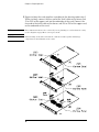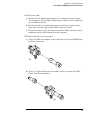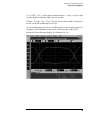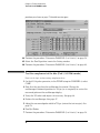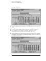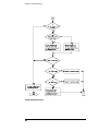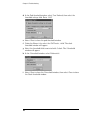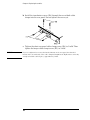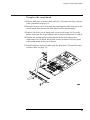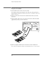
1
Service Guide
Publication number 16760-97013
May 2004
For Safety and Regulatory information see the pages at the end of the book.
© Copyright Agilent Technologies 2001-2004
All Rights Reserved.
Agilent Technologies 16760A Logic
Analyzer
The Agilent 16760A Logic Analyzer—At a Glance
The Agilent Technologies 16760A is a 1500 Mb/s state, 800 MHz timing logic
analyzer module for the Agilent Technologies 16700-series logic analysis system.
The 16760A offers high performance measurement capability.
Features
Some of the main features of the 16760A are as follows:
•
32 data channels
•
2 clock/data channels
•
128 Mb memory depth per channel
•
1500 MHz maximum state acquisition speed
•
800 MHz maximum timing acquisition speed
•
Expandable to 170 channels
Service Strategy
The service strategy for this instrument is the replacement of defective
assemblies. This service guide contains information for finding a defective
assembly by testing and servicing the 16760A state and timing analyzer module.
The modules can be returned to Agilent Technologies for all service work,
including troubleshooting. Contact your nearest Agilent Technologies Sales
Office for more details.
Application
This service guide applies to a 16760A module installed in the 16700-series logic
analysis system mainframes.
2
The 16760A uses operating system version A.02.20.00 or higher. Agilent
Technologies 16700-series mainframes with serial number prefix lower than
US4111 are factory-installed with older operating system versions. If your
mainframe operating system is older than the required version, contact your
Agilent Technologies Service Center for newer software. Refer to “Mainframe and
Operating System” on page 10 for more information.
The 16760A Logic Analyzer
3
In This Book
This book is the service guide for the 16760A 1500 Mb/s state, 800 MHz timing
logic analyzer module.
This service guide has eight chapters.
Chapter 1, “General Information,” beginning on page 9 contains information
about the module and includes accessories for the module, specifications and
characteristics of the module, and a list of the equipment required for servicing
the module.
Chapter 2, “Preparing for Use,” beginning on page 15 tells how to prepare the
module for use.
Chapter 3, “Testing Performance,” beginning on page 31 gives instructions on
how to test the performance of the module.
Chapter 4, “Calibrating,” beginning on page 99 contains calibration instructions
for the module (if required).
Chapter 5, “Troubleshooting,” beginning on page 101 contains explanations of
self-tests and flowcharts for troubleshooting the module.
Chapter 6, “Replacing Assemblies,” beginning on page 127 tells how to replace
the module and assemblies of the module and how to return them to Agilent
Technologies.
Chapter 7, “Replaceable Parts,” beginning on page 137 lists replaceable parts,
shows an exploded view, and gives ordering information.
Chapter 8, “Theory of Operation,” beginning on page 143 explains how the
analyzer works.
4
Contents
1 General Information
Accessories 10
Mainframe and Operating System 10
Specifications 11
Characteristics 12
Environmental Characteristics 12
Recommended Test Equipment 13
2 Preparing for Use
Power Requirements 16
Operating Environment 16
Storage 16
To inspect the module 16
To prepare the mainframe 17
To configure a one-card module 18
To configure a multi-card module 20
To install the module 26
To turn on the system 28
To test the module 28
To clean the module 29
3 Testing Performance
To assemble the SMA/Flying Lead test connectors
34
16760A Minimum Data Eye Width and Minimum Clock Interval Performance Test
Procedure 38
Equipment Required
39
Prepare the logic analysis system for testing
40
Initialize the test equipment for minimum data eye width/minimum clock interval
test 42
Connect the test equipment for the minimum clock interval/minimum eye width
test 44
Set up the test equipment
47
Verify and adjust 8133A pulse generator DC offset
Deskew the oscilloscope 48
Adjust the measured pulse width to 1.5 ns 49
47
5
Contents
Configure the logic analysis system
51
Adjust sampling positions using Eye Finder
Re-aligning a stray channel 57
Test Pod 1 in 200 Mb/s mode
56
59
Determine PASS/FAIL (1 of 2 tests) 59
Open and configure the Listing window. 59
Determine PASS/FAIL (2 of 2 tests) 61
Test the complement of the bits (200 Mb/s mode)
Test Pod 2 in 200 Mb/s mode
63
65
Test the complement of the bits (Pod 2, 200 Mb/s mode)
Test Pod 1 in the 400 Mb/s mode
66
67
Determine and set Eye Finder Position (400 Mb/s mode) 68
Test the complement of the bits (Pod 1, 400 Mb/s mode) 70
Test Pod 2 in 400 Mb/s mode
71
Test the complement of the bits (Pod 2, 400 Mb/s mode)
Test Pod 1 in the 800 Mb/s mode
72
73
Adjust the measured pulse width to 750 ps 73
Determine and set Eye Finder Position (800 Mb/s mode) 75
Test the complement of the bits (Pod 1, 800 Mb/s mode) 77
Test Pod 2 in 800 Mb/s mode
79
Test the complement of the bits (Pod 2, 800 Mb/s mode)
Test Pod 1 in the 1250 Mb/s mode
80
81
Determine and set Eye Finder Position (1250 Mb/s mode) 82
Test the complement of the bits (Pod 1, 1250 Mb/s mode) 84
Test Pod 2 in 1250 Mb/s mode
85
Test the complement of the bits (Pod 2, 1250 Mb/s mode)
Test Pod 1 in the 1500 Mb/s mode
86
87
Adjust the measured pulse width to 600 ps 88
Determine and set Eye Finder Position (1500 Mb/s mode) 90
Test the complement of the bits (Pod 1, 1500 Mb/s mode) 91
Test Pod 2 in 1500 Mb/s mode
93
Test the complement of the bits (Pod 2, 1500 Mb/s mode)
To test the multi-card module
6
95
94
Contents
Performance Test Record
96
4 Calibrating
Calibration Strategy
100
5 Troubleshooting
To use the flowcharts 102
To run the self-tests 105
Self-Test Descriptions 106
To exit the test system 112
To test the cables using an Agilent E5378A Single-ended Probe 113
To test the cables using an Agilent E5379A Differential Probe 121
6 Replacing Assemblies
Tools Required 128
To remove the module 128
To remove the logic analyzer cable 130
To install the logic analyzer cable 131
To replace the circuit board 133
To replace the module 134
To return assemblies 136
7 Replaceable Parts
Replaceable Parts Ordering 138
Replaceable Parts List 139
Exploded View 141
E5382A Accessories 142
8 Theory of Operation
Block-Level Theory
144
Index
7
8
1
General Information
This chapter lists the accessories, the specifications and characteristics, and the
recommended test equipment.
9
Chapter 1: General Information
Accessories
One or more of the following accessories, not supplied, are required to operate
the 16760A logic analyzer.
Accessories
Agilent Part Number
Single-ended soft touch probe
Differential soft touch probe
100-pin single-ended probe
100-pin differential probe
38-pin single-ended probe
Single-ended flying lead probe set
Differential flying lead probe set
E5390A
E5387A
E5378A
E5379A
E5380A
E5382A
E5381A
Mainframe and Operating System
The 16760A logic analyzer requires an Agilent Technologies 16700-series logic
analysis system with operating system version A.02.20.00 or higher. However, the
specifications apply to operating system version A.02.60.00 or higher. The
mainframe operating system must be upgraded to version A.02.60.00 before
attempting the performance verification procedure in Chapter 3. Request a
software upgrade at http://software.cos.agilent.com/16700 or by contacting your
nearest Agilent Technologies Customer Support Center. Agilent Technologies
16700-series mainframes with serial number prefix lower than US4148 are
factory-installed with operating system versions older than A.02.60.00.
Three Cooling Fans Required in Mainframe
Earlier versions of the 16700A/01A/02A mainframe contained only two cooling
fans and might not provide adequate cooling to ensure reliable performance. If
the first six digits of the 16700A/02A serial number (located on the back of the
instrument) are US3849 or higher, or the first six digits of the 16701A are US3902
or higher, the instrument is a three-fan model, which will supply sufficient
cooling.
All 16700B/01B/02B systems already have three cooling fans which provide
adequate cooling to ensure reliable performance.
10
Chapter 1: General Information
Specifications
The specifications are the performance standards against which the product is
tested.
Setup/Hold Window:
tWidth
Individual
Data Channel
vHeight
Data Eye
tSetup
tHold
vThreshold
0V
Sampling
Position
* User Adjustable
tSample*
Clock Channel
16760b05
Specifications for each input
Minimum
Parameter
Data
to
Clock
1500
Mb/s
1250
Mb/s
800
Mb/s
400
Mb/s
200
Mb/s
Description/Notes
tWidth*
500 ps
1.25 ns
Eye width in system under test**
tSetup
250 ps
625 ps
Data setup time required before tSample
tHold
250 ps
625 ps
Data hold time required after tSample
*Specified for an input signal ≤ 800 mV peak-to-peak voltage swing 1V/ns slew rate, using an Agilent E5378A or E5382A probe.
**Eye width and height are specified at the probe tip. Eye width as measured by eye finder in the analyzer may be less.
11
Chapter 1: General Information
Characteristics
The characteristics are not specifications, but are included as additional
information.
Threshold Accuracy
±(30 mV+1.0% of threshold setting)
Speed/Depth/Channel Count
Full Channel
Half Channel
Maximum Conventional Timing Rate
Memory Depth
Channel Count per Card
Channel Count per Five-Card Module
400 MHz
64 M
34
170
800 MHz
128 M
17
85
Environmental Characteristics
Probes
Maximum Input Voltage
± 40 V, CAT I, CAT I = Category I,
secondary power line isolated circuits.
Auxiliary Power
Power Through Cables
1/3 amp at +5 V maximum per cable.
Operating Environment
Temperature
Humidity
Altitude
Vibration
Instrument, 0 °C to 50 °C (+32 °F to 122 °F).
Probe lead sets and cables, 0 °C to 55 °C (+32 °F to 149 °F).
Instrument, probe lead sets, and cables, up to 95% relative humidity
at +40 °C (+122 °F). Non-condensing.
To 3000 m (10,000 ft).
Operating: Random vibration 5 to 500 Hz, 10 minutes per axis,
≈0.2 g (rms).
Non-operating: Random vibration 5 to 500 Hz, 10 minutes per axis,
≈2.41 g (rms); and swept sine resonant search, 5 to 500 Hz, 0.5 g
(0-peak), 5 minute resonant dwell at 4 resonances per axis.
Operating power supplied by mainframe.
Indoor use only.
Pollution Degree 2.
12
Chapter 1: General Information
Recommended Test Equipment
Equipment Required
Equipment
Critical Specifications
Recommended Agilent
Model/Part
Use
Probe Adapter
no substitute
E5378A
P,T
Probe Adapter (Qty 2)*
no substitute
E5382A
P, T
Ground Clips (Qty 10)
no substitute
16517-82105 (pkg of 20)
T
Stimulus Board
no substitute
16760-60001
T
Pulse Generator
750 MHz, 666.6 ps pulse width,
< 120 ps rise time
8133A Option 003
P,T
Digitizing Oscilloscope
≥11 GHz bandwidth, <31.8 ps rise time
54750A mainframe with
54751A plug-in module
P
Test connectors**
no substitute
150 ps Transition Time
Converters (Qty 4)
See page 39.
20:1 Probes (Qty 2)
P
Agilent or HP 15435A
P
54006A
T
SMA Coax Cable (Qty 3)
≥ 18 GHz bandwidth
8120-4948
P
BNC Coax Cable
BNC (m-m), >2 GHz bandwidth
8120-1840
P
Adapter
SMA(m)-BNC(f)
1250-1200
P
P = Performance Tests, T = Troubleshooting
*For a multicard module, one probe adapter per card is required.
**Instructions for making these test connectors are in Chapter 3.
13
Chapter 1: General Information
14
2
Preparing for Use
This chapter gives you instructions for preparing the logic analyzer module for
use.
15
Chapter 2: Preparing for Use
Power Requirements
All power supplies required for operating the logic analyzer are supplied through
the backplane connector in the mainframe.
Operating Environment
The operating environment is listed on page 12. Note the non-condensing
humidity limitation. Condensation within the instrument can cause poor
operation or malfunction. Provide protection against internal condensation.
The logic analyzer module will operate at all specifications within the
temperature and humidity range given on page 12. However, reliability is
enhanced when operating the module within the following ranges:
Temperature: +20 °C to +35 °C (+68 °F to +95 °F)
Humidity: 20% to 80% non-condensing
Storage
Store or ship the logic analyzer in environments within the following limits:
•
Temperature: -40 °C to +75 °C (-40 °F to +167 °F)
•
Humidity: Up to 90% at 65 °C
•
Altitude: Up to 15,300 meters (50,000 feet)
Protect the module from temperature extremes which cause condensation on the
instrument.
To inspect the module
1 Inspect the shipping container for damage.
If the shipping container or cushioning material is damaged, keep them until you
have checked the contents of the shipment and checked the instrument
mechanically and electrically.
2 Check the supplied accessories.
One or more of the accessories listed on page 10 are required to operate the
16760A logic analyzer module.
3 Inspect the product for physical damage.
Check the module and the supplied accessories for obvious physical or
16
Chapter 2: Preparing for Use
mechanical defects. If you find any defects, contact your nearest Agilent
Technologies Sales Office. Arrangements for repair or replacement are made, at
Agilent Technologies' option, without waiting for a claim settlement.
To prepare the mainframe
CAUTION:
Turn off the mainframe power before removing, replacing, or installing the module.
CAUTION:
Electrostatic discharge can damage electronic components. Use grounded wrist-straps
and mats when performing any service to this module.
1 Remove power from the instrument.
a Exit all logic analysis sessions. In the session manager, select
Shutdown.
b At the query, select Power Down.
c When the “OK to power down” message appears, turn the instrument
off.
d Disconnect the power cord.
e Disconnect any input or output connections.
2 Plan your module configuration.
If you are installing a one-card module, use any available slot in the mainframe.
If you are installing a multi-card module, use adjacent slots in the mainframe.
3 Loosen the thumb screws.
Cards or filler panels below the slots intended for installation do not have to be
removed.
Starting from the top, loosen the thumb screws on filler panels and cards that
need to be moved.
17
Chapter 2: Preparing for Use
4 Starting from the top, pull the cards and filler panels that need to be
moved halfway out.
CAUTION:
All multi-card modules will be cabled together. Pull these cards out together.
5 Remove the cards and filler panels.
Remove the cards or filler panels that are in the slots intended for the module
installation. Push all other cards into the card cage, but not completely in. This is
to get them out of the way for installing the module.
Some modules for the Logic Analysis System require an operational accuracy
calibration if you move them to a different slot. For calibration information, refer
to the manuals for the individual modules.
To configure a one-card module
•
When shipped separately, the module is configured as a one-card module. The cables
should be connected as shown in the figure.
•
To configure a multicard module into one-card modules, remove the cables
connecting the cards. Then connect the free end of the 2x10 cable to the connector
labeled "Master" (J6) on each card (see figure below).
18
Chapter 2: Preparing for Use
CAUTION:
If you pull on the flexible ribbon part of the 2x10 cable, you might damage the cable
assembly. Using your thumb and finger, grasp the ends of the cable connector. Apply
pressure to the ends of the cable connector to disengage the metal locking tabs of the
connector from the cable socket on the board. Then pull the connector from the cable
socket.
NOTE:
Save unused cables for future configurations.
19
Chapter 2: Preparing for Use
To configure a multi-card module
1 Plan the configuration. Multicard modules can only be connected as shown
in the illustration. Expander cards are evenly distributed above and below
the master card. Select the card that will be the master card, and set the
remaining cards aside.
2 Obtain two 2x40 cables from the accessory pouch for every expander card
being configured.
One Expander: Two 2x40 cables
Two Expanders: Four 2x40 cables
Three Expanders: Six 2x40 cables
Four Expanders: Eight 2x40 cables.
20
Chapter 2: Preparing for Use
3 Connect a 2x40 cable to J9 and to J10 of each card in the multicard
configuration.
4 On the expander cards, disconnect the end of the 2x10 cable that is
plugged into the connector labeled "Master."
CAUTION:
If you pull on the flexible ribbon part of the 2x10 cable, you might damage the cable
assembly. Using your thumb and finger, grasp the ends of the cable connector. Apply
pressure to the ends of the cable connector to disengage the metal locking tabs of the
connector from the cable socket on the board. Then pull the connector from the cable
socket.
21
Chapter 2: Preparing for Use
5 Begin stacking the cards together according to the drawing under step 1.
While stacking, connect the free end of the 2x40 cable on the lower card
J9 to J500 of the upper card, on the underside of the card. Connect the
free end of the 2x40 cable on the lower card J10 to J501 of the upper card,
on the underside of the card.
NOTE:
These instructions show a five-card set. If you are planning a set of less than five cards,
see the diagram on page 20 for correct placement.
CAUTION:
When stacking cards, make sure that the cards do not rub together and damage
components on the underside of the cards.
22
Chapter 2: Preparing for Use
6 Feed the free end of the 2x10 cables of the lower expander cards through
the access holes to the master card. Plug the 2x10 cables into J4 (bottommost expander in a five-card configuration) and J5 (expander that is next
to the master card) on the master card.
Expander
Master
Expander
23
Chapter 2: Preparing for Use
7 Stack the remaining expander boards on top of the master board. While
stacking, connect the free end of the 2x40 cables on the lower card J10
and J9 to the upper card J501 and J500.
24
Chapter 2: Preparing for Use
8 Feed the free end of the 2x10 cables of the expander cards through the
access holes to the master card. Plug the 2x10 cables into J7 (expander
that is next to the master card) and J8 (top-most expander in a four- or
five-card configuration) on the master card.
Expander
Expander
Master
Expander
Expander
Expander
25
Chapter 2: Preparing for Use
To install the module
1 Slide the cards above the slots for the module about halfway out of the
mainframe.
2 With the probe cables facing away from the instrument, slide the module
approximately halfway into the mainframe.
3 Slide the complete module into the mainframe, but not completely in.
Each card in the instrument is firmly seated and tightened one at a time in step 5.
4 Position all cards and filler panels so that the endplates overlap.
26
Chapter 2: Preparing for Use
5 Seat the cards and tighten the thumbscrews.
Starting with the bottom card, firmly seat the cards into the backplane connector
of the mainframe. Keep applying pressure to the center of the card endplate
while tightening the thumbscrews finger-tight. Repeat this for all cards and filler
panels starting at the bottom and moving to the top.
CAUTION:
Correct air circulation keeps the instrument from overheating. For correct air circulation,
filler panels must be installed in all unused card slots. Keep any extra filler panels for
future use.
27
Chapter 2: Preparing for Use
To turn on the system
1 Connect the power cable to the mainframe.
2 Turn on the instrument power switch.
When you turn on the instrument power switch, the instrument performs
powerup tests that check mainframe circuitry. After the powerup tests are
complete, the screen will look similar to the sample screen below.
To test the module
The logic analyzer module does not require an operational accuracy calibration or
adjustment. After installing the module, you can test and use the module.
•
If you require a test to verify the specifications, see “Testing Performance” on page 31.
•
If you require a test to verify correct module operation using software self-tests, see
“To run the self-tests” on page 105.
•
If the module does not operate correctly, see “Troubleshooting” on page 101.
28
Chapter 2: Preparing for Use
To clean the module
•
With the mainframe turned off and unplugged, use a cloth moistened with a mixture
of mild detergent and water to clean the rear panel.
•
Do not attempt to clean the module circuit board.
29
Chapter 2: Preparing for Use
30
3
Testing Performance
This chapter tells you how to test the performance of the logic analyzer against
the specifications.
31
Chapter 3: Testing Performance
To ensure the logic analyzer is operating as specified, software tests (self-tests)
and manual performance tests are done. The logic analyzer is considered
performance-verified if all of the software tests and manual performance tests
have passed. The procedures in this chapter indicate what constitutes a “Pass”
status for each of the tests.
Test Strategy
This chapter shows the module being tested in an Agilent Technologies 16700Bseries mainframe. For a complete test, start at the beginning with the software
tests and continue through to the end of the chapter. For an individual test,
follow the procedure in the test.
Only specified parameters are tested. Specifications are listed on page 11. The
test conditions defined in this procedure ensure that the specified parameter is
as good as or better than specification. No attempt is made to determine
performance which is better than specification. Not all channels of the logic
analyzer will be tested; rather a sample of channels is tested. A calibration
laboratory may choose to elaborate on these tests and test all channels at their
discretion.
One-card Module. To perform a complete test on a one-card module, start at
the beginning of the chapter and follow the test procedure.
Multi-card Module. To perform a complete test on a multi-card module,
perform the self-tests (page 40) with the cards connected. Then, remove the
multi-card module from the mainframe and configure each card as a one-card
module. Install the one-card modules into the mainframe and perform the
performance verification tests on each card. When the tests are complete,
remove the one-card modules, reconfigure them into their original multi-card
module configuration, reinstall it into the mainframe and perform the self-tests
again.
For removal instructions see Chapter 6, “Replacing Assemblies,” beginning on
page 127. For installation and configuration instructions see Chapter 2,
“Preparing for Use,” beginning on page 15.
Test Interval
Test the performance of the module against specifications at two-year intervals.
Test Record Description
A performance test record for recording the results of each procedure is located
at the end of this chapter.
32
Chapter 3: Testing Performance
Test Equipment
Each procedure lists the recommended test equipment. You can use equipment
that satisfies the specifications given. However, the procedures are based on
using the recommended model or part number.
Instrument Warm-Up
Before testing the performance of the module, warm-up the instrument and the
test equipment for 30 minutes.
33
Chapter 3: Testing Performance
To assemble the SMA/Flying Lead test connectors
To assemble the SMA/Flying Lead test connectors
The SMA/Flying Lead test connectors provide a high-bandwidth connection
between the logic analyzer and the test equipment. The following procedure
explains how to fabricate the four required test connectors.
Materials Required
Material
Critical Specification
SMA Board Mount Connector
(Qty 8)
Recommended Model/Part
Johnson 142-0701-801
(ref: www.johnsoncomponents.com)
Pin Strip Header
(Qty 1, which will be separated)
.100" X .100" Pin Strip Header, right 3M 2380-5121TN or similar 2- row
angle, pin length .230", two rows, with 0.1” pin spacing
.120" solder tails
SMA 50 ohm terminators
(Qty 2)
Minimum bandwidth 2 GHz
SMA m-m adapter
(Qty 4)
Johnson 142-0801-866 50 ohm
Dummy Load Plug
Johnson 142-0901-811 SMA Plug to
Plug or similar
1 Prepare the pin strip header:
a Cut or cleanly break a 2 x 2 section from the pin strip.
34
Chapter 3: Testing Performance
To assemble the SMA/Flying Lead test connectors
b Trim about 1.5 mm from the pin strip inner leads and straighten them
so that they touch the outer leads.
c Trim about 2.5 mm from the outer leads.
solder
d Using a very small amount of solder, tack each inner lead to each outer
lead at the point where they are touching.
35
Chapter 3: Testing Performance
To assemble the SMA/Flying Lead test connectors
2 Solder the pin strip to the SMA board mount connector:
a Solder the leads on the left side of the pin strip to the center conductor
of the SMA connector as shown in the diagram below.
b Solder the leads on the right side of the pin strip to the inside of the
SMA connector’s frame as shown in the diagram below. Use a small
amount of solder.
3 Attach the second SMA board mount connector:
a Re-heat the solder connection made in the previous step, and attach
the second SMA connector, as shown in the diagram below. Note that
the second SMA connector is upside-down, compared to the first. Add a
little solder to make a good connection.
b Solder the center conductor of the second SMA connector to the center
conductor of the first SMA connector and the leads on the left side of
the pin strip.
solder
c Rotate the assembly 180 degrees and solder the two SMA board mount
connector frames together.
36
Chapter 3: Testing Performance
To assemble the SMA/Flying Lead test connectors
4 Check your work:
a Ensure that the following four points have continuity between them:
The two pins on the left side of the pin strip, and the center conductors
of each SMA connector.
b Ensure that there is continuity between each of the two pins on the
right side of the pin strip, and the SMA connector frames.
c Ensure that there is NO continuity between the SMA connector center
conductor and the SMA connector frame (ground).
5 Finish creating the test connectors:
a Attach an SMA m-m adapter to one end of each of the four SMA/Flying
Lead test connectors.
b Attach a 50 ohm terminator to the other end of just two of the SMA/
Flying Lead test connectors.
37
Chapter 3: Testing Performance
16760A Minimum Data Eye Width and Minimum Clock Interval Performance Test Procedure
16760A Minimum Data Eye Width and Minimum Clock
Interval Performance Test Procedure
The specifications for the 16760A logic analyzer define a minimum data eye width
and a minimum clock interval at which data can be acquired.
Acquisition Mode:
200 Mb/s
400 Mb/s
800 Mb/s
1.25 Gb/s
1.5 Gb/s
Minimum clock interval,
active edge to active edge
5 ns
2.5 ns
1.25 ns
800 ps
667 ps
Minimum data pulse width
1.5 ns
1.5 ns
750 ps
750 ps
600 ps
These tests verify that the logic analyzer meets these specifications.
At each of the five acquisition modes, we will test the minimum data eye width at
the minimum clock interval, thereby testing both specifications at once.
The minimum clock interval is specified from active clock edge to active clock
edge. All tests are performed while clocking data into the logic analyzer on both
rising and falling edges of the clock (double edge clock), so the pulse generator
test frequency will be set to half of the acquisition speed.
Eye Finder is used to adjust the sampling position on every channel. Eye Finder
must be used to achieve minimum data eye width.
38
Chapter 3: Testing Performance
Equipment Required
Equipment Required
The following equipment is required for the performance test procedure.
Equipment Required
Equipment
Critical Specification
Pulse Generator
≥ 765 MHz, two channels, differential
Agilent or HP 8133A option 003
outputs, 150-180 ps rise/fall time (if faster,
use transition time converters).
150 ps Transition Time Converter Required if pulse generator’s rise time is
(Qty 4)
less than 150 ps. (Pulse generator
conditions: Voffset=1V, ∆V=250 mV.)
Required for 8133A opt. 003.
Recommended Model/Part
Agilent or HP 15435A
Oscilloscope
bandwidth ≥ 1.5 GHz,
sampling rate ≥ 8 GSa/s
Agilent or HP 54845A/B or similar
SMA Coax Cable
(Qty 2)
>18 GHz bandwidth
Agilent or HP 8120-4948
Flying Lead Probe Set
(Qty 2)
no substitute
Agilent E5382A
Male BNC to Female SMA
adapters
(Qty 2)
Cambridge Products CP-AD507
(ref: www.cambridgeproducts.com)
SMA/Flying Lead test connectors, no substitute
(f) SMA to (f) SMA to Flying Lead
Probe
(Qty 4)
See “To assemble the SMA/Flying Lead
test connectors” on page 34
39
Chapter 3: Testing Performance
Prepare the logic analysis system for testing
Prepare the logic analysis system for testing
1 Turn on the logic analysis system.
a Connect the keyboard and monitor to the rear panel of the logic
analysis mainframe (16700B only).
b Connect the mouse to the rear panel of the mainframe.
c Plug in the power cord to the power connector on the rear panel of the
mainframe.
d Turn on the main power switch on the mainframe front panel.
While the logic analysis system is booting, observe the boot dialogue for the following:
•
ensure all of the installed memory is recognized
•
any error messages
•
interrupt of the boot process with or without error message
A complete transcript of the boot dialogue is in the Agilent Technologies 16700Bseries Logic Analysis System Service Guide, Chapter 8, "Theory of Operation.”
2 During initialization, check for any failures.
If an error or an interrupt occurs, refer to the Agilent Technologies 16700B-series
Logic Analysis System Service Guide, Chapter 5, "Troubleshooting.” Note that if an
Agilent 16760A module is temporarily installed in a mainframe only to test the
performance of the module, then the mainframe may report that the module will
require an operational accuracy calibration. This is expected, and step 4 in this
procedure will clear this error message.
3 Do a self-test on the logic analysis system.
a When the logic analysis system has finished booting and the System
window appears (that is, a session has started), click on the System
Administration icon.
b Under the Admin tab, click on Self-Test... in the query pop-up, select
Yes to exit the current session.
The Self-Test closes the current session because the test algorithms leave the system
in an unknown state. Re-launching the session at the end of the self-test will ensure
the system is properly initialized.
c In the Self-Test window select Test All.
When the tests are finished, the Status will change to Passed or Failed. You can find
detailed information about the test results in the Status Message field of the Self-Test
window.
40
Chapter 3: Testing Performance
Prepare the logic analysis system for testing
Some system CPU board tests may return a status of Untested because they require
user action. Procedures to do these tests are found in the Agilent Technologies
16700B-series Logic Analysis System Service Guide. For the purposes of testing the
Agilent 16760A module performance, running untested system CPU board tests are
not required. If these tests are not done, the Agilent 16760A performance test is not
affected.
d When the self-tests are complete, select Quit to exit the test menu.
e Record a PASS in the Performance Test Record if all module self-tests
pass.
4 Set up the logic analysis system.
a In the Session Manager window, select "Start Session" to re-launch a
logic analysis session.
b In the Logic Analysis System window, select the module icon, then
select Setup and Trigger. A Setup and Trigger window will appear.
c In the Setup and Trigger window, click on the Calibration tab. Follow
the instructions under the Calibration tab to perform an operational
accuracy calibration on the Agilent 16760A module.
Repeat the above step for each single-card Agilent 16760A module installed in the
mainframe that is being tested. If any calibration status returns "failed," then the
Agilent 16760A module requires repair. If the calibration status returns "passed" for
both pods, then record a PASS in the performance test record at the end of this
chapter.
d Proceed to the next section when the operational accuracy calibration
is complete.
41
Chapter 3: Testing Performance
Initialize the test equipment for minimum data eye width/minimum clock interval test
Initialize the test equipment for minimum data eye
width/minimum clock interval test
1 Turn on the required test equipment. Let all of the test equipment and the
logic analyzer warm up for 30 minutes before beginning any test.
2 Set up the pulse generator.
a Set the frequency of the pulse generator. We will test in the 200 Mb/s
mode first.
The logic analyzer will be tested using a double-edge clock. The test
frequency is half the test clock rate because data is acquired on both
the rising edge and the falling edge of the clock. Set the frequency to
100 MHz plus the frequency uncertainty of the pulse generator, plus a
test margin of 1%.
For example, if you are using an 8133A pulse generator, the frequency
accuracy is ±1% of setting. Use a test margin of 1%. Set the frequency
to 100 MHz plus 2% (102 MHz).
b Set the rest of the pulse generator parameters to the values shown in
the following table.
Pulse Generator Setup
Timebase
Pulse Channel 2
Trigger
Pulse Channel 1
Mode: Int
Mode: Pulse ÷ 1
Disable (LED on)
Mode: Square
Freq: was set in Delay: (not available in pulse mode)
previous step. Width: Initially set to 1.5 ns.
Change later (on page 48).
Ampl: 0.25 V
42
Delay: 0 ps
Width: (not available in square
mode)
Ampl: 0.25 V
Offs: 1.0 V
Offs: 1.0 V
Output: Enable (LED off)
Output: Enable (LED off)
Comp: Normal (LED off)
Comp: Normal (LED off)
Limit: Off (LED off)
Limit: Off (LED off)
Output: Enable (LED off)
Output: Enable (LED off)
Chapter 3: Testing Performance
Initialize the test equipment for minimum data eye width/minimum clock interval test
3 Set up the oscilloscope.
a Set up the oscilloscope according to the following tables.
Oscilloscope Setup
Setup: Channel 1
Setup: Ch. 1 Probe
Setup: Channel 2
On
Attenuation: 1.00:1
On
Attenuation: 1.00:1
Scale: 50 mV/div
Units: Volts
Scale: 50 mV/div
Units: Volts
Offset: 1 V
Attenuation Units: Ratio
Offset: 1 V
Attenuation Units: Ratio
Coupling: DC
External Gain: (n/a)
Coupling: DC
External Gain: (n/a)
Input: 50 ohm
Skew: (Set later. See page
47)
Input: 50 ohm
Skew: 0.0 seconds
External Offset: (n/a)
Setup: Ch. 2 Probe
External Offset: (n/a)
Setup: Channel 3
Setup: Channel 4
Off
Off
Setup: Horizontal
Setup: Trigger
Setup: Acquisition
Scale: 500 ps/div
Mode: Edge
Sampling Mode: Equiv. Time Waveforms: Connect dots
Position: 800 ps
Source: Channel 1
Memory Depth: Automatic
Persistence: Minimum
Reference: Center
Level: 1.00 V
Averaging: Enabled
Grid: On (and set intensity)
Delayed: not selected
Edge: Rising Edge
# of Averages: 4
Backlight Saver: as
preferred
Setup: Display
Sweep: Auto
Measure: Markers
Mode: Manual placement
All else: (n/a)
43
Chapter 3: Testing Performance
Connect the test equipment for the minimum clock interval/minimum eye width test
Connect the test equipment for the minimum clock
interval/minimum eye width test
Connect the 16760A Logic Analyzer Pod to the 8133A Pulse
Generator
1 Connect a Transition Time Converter (if required—see page 39) to each of
the four outputs of the 8133A pulse generator: Channel 1 OUTPUT,
Channel 1 OUTPUT, Channel 2 OUTPUT, Channel 2 OUTPUT.
2 Connect the two SMA/Flying Lead test connectors (see “To assemble the
SMA/Flying Lead test connectors” on page 34) with 50 ohm terminators to
the Transition Time Converters at the 8133A pulse generator Channel 1
OUTPUT and Channel 1 OUTPUT. (If Transition Time Converters are not
required, connect the SMA/Flying Lead test connectors directly to the
pulse generator outputs.)
3 Connect the two SMA/Flying Lead test connectors without 50 ohm
terminators to the Transition Time Converters at the 8133A pulse
generator Channel 2 OUTPUT and Channel 2 OUTPUT. (If Transition Time
Converters are not required, connect the SMA/Flying Lead test connectors
directly to the pulse generator outputs.)
4 Connect an E5382A Flying Lead Probe Set to Pod 1 of the 16760A logic
analyzer.
5 Connect the E5382A Flying Lead Probe Set’s CLK lead to the pin strip of
the SMA/Flying Lead connector at the 8133A pulse generator’s Channel 1
OUTPUT.
ground clip
44
Chapter 3: Testing Performance
Connect the test equipment for the minimum clock interval/minimum eye width test
NOTE:
Be sure to use the black ground clip (supplied with the E5382A Flying
Lead Probe Set) and orient the leads so that the black clip is connected to
one of the SMA/Flying Lead connector’s ground pins!
6 Connect the E5382A Flying Lead Probe Set’s CLK lead to the SMA/Flying
Lead connector at the 8133A pulse generator’s Channel 1 OUTPUT. Again,
be sure to use the black ground clip and orient the leads so that the black
clip is connected to ground.
7 Connect the E5382A Flying Lead Probe Set’s bits 6 and 14 to the SMA/
Flying Lead test connector’s pin strip connector at the 8133A pulse
generator’s Channel 2 OUTPUT.
8 Connect the E5382A Flying Lead Probe Set’s bits 2 and 10 to the SMA/
Flying Lead test connector’s pin strip connector at the 8133A pulse
generator’s Channel 2 OUTPUT.
Connect the 8133A Pulse Generator Output to the 54845A
Oscilloscope
9 Attach Male BNC to Female SMA adapters to Channels 1 and 2 on the
54845A oscilloscope.
10 Attach one end of an SMA cable to the Male BNC to Female SMA adapter
on Channel 1 of the oscilloscope.
11 Attach the other end of the SMA cable to the SMA/Flying Lead connector
at the Channel 2 OUTPUT of the 8133A pulse generator.
12 Attach one end of the other SMA cable to the Male BNC to Female SMA
adapter on Channel 2 of the oscilloscope.
13 Attach the other end of the SMA cable to the SMA/Flying Lead connector
at the Channel 2 OUTPUT of the 8133A pulse generator.
45
Chapter 3: Testing Performance
Set up the test equipment
Set up the test equipment
Next, verify and adjust the pulse generator’s DC offset, deskew the oscilloscope,
and measure and adjust the pulse width.
Verify and adjust 8133A pulse generator DC offset
1 On the 54845A oscilloscope, select Measure from the menu bar at the top
of the display.
2 Select Markers...
3 In the Markers Setup window set marker “Ay” to 0.875 V, and set marker
“By” to 1.125 V.
4 Observe the waveforms on the oscilloscope display. If they are not
centered within the “Ay” and “By” markers, adjust the 8133A pulse
generator’s Channel 2 OFFSET until the waveforms are centered as well as
possible. (The resolution of the 8133A OFFSET setting is 20 mV.)
46
Chapter 3: Testing Performance
Set up the test equipment
Deskew the oscilloscope
This procedure neutralizes any skew in the oscilloscope’s waveform display.
1 On the 54845A oscilloscope, change the Horizontal scale from 500 ps/div
to 200 ps/div. You can do this using the large knob in the Horizontal setup
section of the front panel.
2 Select Setup from the menu bar at the top of the oscilloscope display.
3 Select Channel 1.
4 Select Probes.
NOTE:
If the Probes dialog obscures the waveform display, select Utilities, User
Preferences..., and in the Dialog section choose Transparent. Then
position the Probes dialog so you can see the horizontal crossings of the
waveforms.
5 Select Skew </> to deskew Channel 1 and Channel 2 signals so that both
channels cross the 54845A horizontal center line at the same time, at both
ends of the eye (both crossings of the horizontal center line). The
47
Chapter 3: Testing Performance
Set up the test equipment
horizontal center of the graticule line is at 1 volt because the vertical offset
was set to 1 volt in the oscilloscope setup described on page 43.
6 Select Close in the Probe Setup window.
7 Select Close in the Channel Setup window.
Adjust the measured pulse width to 1.5 ns
The pulse generator’s pulse width was set to 1.5 ns (in the setup on page 42). In
this procedure, you will use the oscilloscope’s measurement markers to measure
the actual pulse width in the test setup. Then you will adjust the pulse generator
so that the measured pulse width is as specified.
1 Observe the 54845A oscilloscope display. Change the Channel 2 pulse
width of the 8133A pulse generator so that the pulse width measured at 1
volt on the oscilloscope is equal to 1.5 ns minus the measurement
uncertainty and display resolution of the oscilloscope, further reduced by
35 ps for test margin.
If you are using the 54845A/B oscilloscope, the measurement uncertainty
48
Chapter 3: Testing Performance
Set up the test equipment
is ±((0.007% * ∆t) + (full scale/2x memory depth) + 30 ps) ≅ ±30 ps. Add
5 ps for display resolution. Add 35 ps test margin.
1500 ps - 30.15 ps - 5 ps - 35 ps = 1430 ps. Set the pulse width as measured
on the 54845A/B oscilloscope to 1430 ps.
On the oscilloscope move the Ax and Bx markers to the crossing points of
the pulse and the horizontal center line. Read the pulse width at the
bottom of the oscilloscope display. It is displayed as “∆=”.
49
Chapter 3: Testing Performance
Configure the logic analysis system
Configure the logic analysis system
1 Configure the Sampling settings.
a In the Agilent 16700-series logic analysis system’s System window,
select the 16760A logic analyzer icon, then select “Setup and Trigger”.
A Setup and Trigger window will appear.
b In the logic analyzer Setup and Trigger window, select the Sampling tab
(if it is not already selected).
c Under the Sampling tab, select State Mode.
d Under State Mode Controls, select the “200 Mb/s / 32 M State” mode.
e Under Clock Setup, at the bottom of the Clock J column, select the
clock edge field and set the J clock to “Both Edges”.
clock
edge
field
2 Configure the Acquisition settings.
a In the logic analyzer Setup and Trigger window, select the Trigger tab.
b Under the Trigger tab, select the Settings subtab.
c Select the Acquisition Depth field, then select 128K.
d Select the Trigger Position field, then select Start.
50
Chapter 3: Testing Performance
Configure the logic analysis system
e Select the Count field, then select Off.
3 Configure the Format settings.
a In the logic analyzer Setup and Trigger window, select the Format tab.
b Under the Format tab, select Pod Assignment.
c In the Pod Assignment window, use the mouse to drag the pod from the
Unassigned Pods column to the Analyzer 1 column.
d Select Close to close the Pod Assignment window.
e Under the Format tab, use the scroll bar to scroll to the right so you can
51
Chapter 3: Testing Performance
Configure the logic analysis system
see the fields for Pod 1.
channel
assignment
field
scroll
bar
f Select the channel assignment field for the pod being tested, then
select Individual in the pop-up menu.
g Using the mouse, select each asterisk to un-assign all data channels on
the pod. Ensure all channels are un-assigned on all pods. Now assign
channels 2, 6, 10, and 14 for the pod being tested (Pod 1). An asterisk
(*) means that a channel is assigned.
h Select OK to close the channel assignment window.
4 Configure the clock and data thresholds.
52
Chapter 3: Testing Performance
Configure the logic analysis system
a Select the pod threshold field for the pod that you are going to test. The
Pod threshold window will appear. You must have the E5382A Flying
Lead Probe attached to the pod you will be testing so that the pod
threshold dialog will appear when you select the pod threshold field.
pod
threshold
field
b In the Pod threshold window, select User Defined and set the threshold
value to 1 volt. The “Apply threshold settings to all pods” check box
doesn’t matter.
c Select Close to close the Pod threshold window.
d Under the Format tab, use the scroll bar at the bottom of the window to
53
Chapter 3: Testing Performance
Configure the logic analysis system
scroll to the left and select “Clk Thresh...”.
clock
threshold
button
scroll
bar
e In the Clock Thresholds window, select the J clock threshold button,
then in the J threshold window select Differential.
f Select Close to close the J threshold window. Select Close to close the
Clock Thresholds window.
5 Configure the Trigger settings.
a In the logic analyzer Setup and Trigger window, under the Trigger tab,
select the Trigger Functions subtab.
b Select “Find pattern n times.”
c Select the Replace button.
54
Chapter 3: Testing Performance
Configure the logic analysis system
d Enter “A” in the “Label 1 =” field.
Adjust sampling positions using Eye Finder
1 In the Setup and Trigger window, select the Sampling tab, then select the
“Sampling Positions...” button (which is in the Clock Setup area of the
window). The Eye Finder window will appear. Ensure that the “Sampling
Positions” tab is selected.
2 From the menu bar in the Eye Finder window, select Results.
3 Select “Remove All Eye Finder Data” if this selection is available (if it is
not ghosted). Select “Yes” to confirm that you want to remove the data.
4 Select Label1, then select Expand (if not already expanded).
5 If the blue bars in the Eye Finder display are not vertically aligned:
a Grab the right-most blue bar in the “Label1 (4 channels)” row with the
mouse pointer and move it all the way to the left and release the mouse
button. This will vertically align all of the blue bars.
6 Select the Sampling Positions tab in the Eye Finder window.
7 Using the mouse pointer, grab the blue bar for “Label 1 (4 channels)” and
55
Chapter 3: Testing Performance
Configure the logic analysis system
move it to the recommended starting position of 0.6 ns. All of the blue bars
will follow.
8 Select Run Eye Finder (the large green bar).
9 Ensure that an eye appears for each bit near the recommended starting
position. Depending on your test setup, the eye position may vary. Any
skew between channel 1 and channel 2 of your pulse generator will cause
the eye position to shift to the left or right in the Eye Finder display. A
shift of up to 0.5 ns should be considered normal. The important point is
that your Eye Finder display should look similar to the picture below
(although it may be shifted left or right), and Eye Finder must be able to
place the blue bars in the narrow eye.
Re-aligning a stray channel
If the blue bar for a particular bit does not appear in its eye near the
recommended starting position, then do the following steps to realign the
sampling position of the stray channel. In the following example, the
sampling position of one channel (Label1 [2]) must be realigned with the
sampling position of the other channels. (The following example shows the
56
Chapter 3: Testing Performance
Configure the logic analysis system
analyzer in the 1500 Mb/s mode.)
1 Using the mouse, drag the sample position (blue line) of a stray channel so
that it is in the same eye as the other channels (drag channel Label1 [2] in
the above example). The Suggested Position from Eye Finder (green
triangle) will also move to the new eye.
2 Repeat the above step for all remaining stray channels.
3 Select Run Eye Finder. Eye Finder will recalculate the new sample
positions based on the sample position changes. The following example
shows all sampling positions aligned and in the correct eye (with the
analyzer in the 1500 Mb/s mode).
57
Chapter 3: Testing Performance
Test Pod 1 in 200 Mb/s mode
Test Pod 1 in 200 Mb/s mode
The steps that follow include pass/fail criteria.
Determine PASS/FAIL (1 of 2 tests)
1 PASS/FAIL: If an eye exists near the recommended starting position for
every bit, and Eye Finder places a blue bar in the eye for each bit, then the
logic analyzer passes this portion of the test.
2 If an eye does not exist near the recommended starting position for every
bit or Eye Finder cannot place the blue bar in the eye, then the logic
analyzer fails the test. Record the failure in the test record (shown on page
95).
Open and configure the Listing window.
a In the Setup and Trigger window, select Window from the menu bar,
then select Slot n: Analyzer<n> (where n is the slot where the module
under test is installed). At the pop-up menu, select Listing. The Listing
window will appear.
58
Chapter 3: Testing Performance
Test Pod 1 in 200 Mb/s mode
b In the Listing window, select the Markers tab.
c Select the G1: button and the Markers Setup window will appear.
d Select the field immediately to the right of G1, and select Pattern.
e Select the field immediately to the right of G2, and select Pattern.
f Right-click on the Interval field (which is below G1 and G2) and select
Delete.
g Select the field immediately to the right of “Data at” and select
Beginning.
NOTE:
Leave the marker Setup window open. You will be entering numeric values
in the "occurs" field after acquiring the first run of test data.
1 Configure the Markers.
a In the logic analyzer Listing window, select the Run icon. This will load
the logic analyzer memory with data so the markers can be configured.
An error message will appear because the marker patterns are not yet
specified.
59
Chapter 3: Testing Performance
Test Pod 1 in 200 Mb/s mode
b Select OK to close the error message window.
c In the Marker Setup window, select the G1 Define... button. The
“Marker Pattern for <G1>” window will appear. In the pattern field,
enter "a", then select Close.
d In the Marker Setup window, select the G2 Define... button. The G2
Marker Pattern window will appear. In the pattern field, enter "5", then
select Close.
e In the Marker Setup window, select the 'occurs' value field that
corresponds to marker G1. Enter 65535.
f In the Marker Setup window, select the 'occurs' value field that
corresponds to marker G2. Enter 65535, then press Enter.
g Select Close.
2 In the Listing window, Select the Run Repetitive icon. The analyzer will
run and the listing window will update every few seconds.
Determine PASS/FAIL (2 of 2 tests)
Pass/Fail Point: The Listing window is set up to search for the appropriate
number of A's and 5's in the acquisition. If the logic analyzer does not
detect the correct number of A’s and 5’s, an error window will appear. The
window will be named 'Error - Listing', and it will say “Pattern NOT found
60
Chapter 3: Testing Performance
Test Pod 1 in 200 Mb/s mode
for marker...”.
1 Let the logic analyzer run repetitive for about 1 minute. If no error
message is displayed the test passes.
If the red error window “Error- Listing <1> Pattern NOT found...” appears
during the minute or so that it runs repetitively, then the logic analyzer
fails the test. Record the failure in the appropriate place on the test
record.
NOTE:
Be sure that the black ground clip is making good contact with the ground
pin on the test connector.
2 After approximately 1 minute select the red stop button in the Listing
window.
61
Chapter 3: Testing Performance
Test Pod 1 in 200 Mb/s mode
NOTE:
As a point of curiosity, you may want to determine the absolute minimum
pulse width and/or absolute maximum frequency at which data can be
acquired. The “Performance Test Record” on page 95 does not include
places for recording these values because the Performance Verification
procedure only verifies that the logic analyzer meets specifications.
Determination of additional parameters is not required, but may be
performed at the discretion of the calibration laboratory.
On some pulse generators, the signal outputs may become slightly
unstable for a very short period of time when the signal parameters are
adjusted. Adjusting the pulse generator while the logic analyzer is running
can cause a false failure.
If the Pattern NOT found error message appears while making an
adjustment to the pulse generator select OK to close the window. If the
message appears again after you have stopped adjusting the pulse
generator and allowed a short settling time for the pulse generator, then
the logic analyzer fails the test.
Test the complement of the bits (200 Mb/s mode)
Now test the logic analyzer using complement data.
1 On the 8133A pulse generator, in the PULSE setup for CHANNEL 2, select
COMP.
2 Note that the signal on the oscilloscope has moved. Change the
oscilloscope’s horizontal position to -600 ps (or as required) to center the
measured pulse on the oscilloscope display.
3 Verify the DC offset and adjust it if necessary. See page 46.
4 Deskew the oscilloscope if necessary. See page 47.
5 Adjust the oscilloscope’s measurement markers to measure the pulse
width. Set the markers so that ∆=1430 ps (this assumes you are using the
8133A pulse generator and the Infiniium oscilloscope). Adjust the pulse
generator so that the pulse width is 1430 ps as measured by the markers.
62
Chapter 3: Testing Performance
Test Pod 1 in 200 Mb/s mode
See page 48 for details.
6 Adjust the sampling positions (run Eye Finder). See page 55.
7 Determine pass or fail (1 of 2 tests). See page 58.
8 Ensure that the Listing window is set up. See page 58.
9 Select the Run Repetitive icon in the Listing window.
10 Determine pass or fail (2 of 2 tests). See page 60.
63
Chapter 3: Testing Performance
Test Pod 2 in 200 Mb/s mode
Test Pod 2 in 200 Mb/s mode
1 Leave the first E5382A Flying Lead Probe Set connected to Pod 1 of the
logic analyzer. Remove the Pod 1 flying leads 2, 6, 10, and 14 from the
SMA/Flying Lead test connectors. Do not remove the flying leads that are
connected to CLK and CLK.
2 Connect the second E5382A Flying Lead Probe Set to Pod 2 of the logic
analyzer.
3 Connect the Pod 2 E5382A Flying Lead Probe Set’s bits 6 and 14 to the
SMA/Flying Lead test connector’s pin strip connector at the 8133A pulse
generator’s Channel 2 OUTPUT.
4 Connect the Pod 2 E5382A Flying Lead Probe Set’s bits 2 and 10 to the
SMA/Flying Lead test connector’s pin strip connector at the 8133A pulse
generator’s Channel 2 OUTPUT.
5 On the 8133A pulse generator, in the PULSE setup for CHANNEL 2, press
the COMP button to return the outputs to normal.
6 Note that the signal on the oscilloscope has moved. Change the
oscilloscope’s horizontal position to 800 ps (or as required) to center the
measured pulse on the oscilloscope display.
7 Verify the DC offset and adjust it if necessary. See page 46.
8 Deskew the oscilloscope if necessary. See page 47.
9 Readjust the pulse width from the pulse generator as measured on the
oscilloscope to 1.5 ns. See page 48.
10 In the logic analyzer’s Setup and Trigger window, Format tab, unassign all
pod 1 bits. A Warning window will appear stating that the trigger function
has become invalid. Select OK to close the Warning window.
11 Assign bits 2, 6, 10, and 14 of Pod 2.
12 Set the Pod 2 threshold to 1 volt (just as you did for Pod 1 on page 53).
13 In the “Setup and Trigger...” window, Format tab, use the scroll bar at the
bottom of the window to scroll to the left. Ensure that the J clock
threshold is set to Differential.
14 Re-establish the trigger function:
a In the logic analyzer’s Setup and Trigger window, select the Trigger tab,
64
Chapter 3: Testing Performance
Test Pod 2 in 200 Mb/s mode
and the Trigger Functions subtab.
b Select “Find pattern n times” and select the “Replace” button.
c Enter “A” in the “Label 1 = “ field.
15 Adjust the sampling positions using Eye Finder. Be sure to expand “Label1
(4 channels)” and use the recommended starting position noted on page
56. Realign any stray channels if necessary. See page 56.
16 Determine pass or fail (1 of 2 tests). See page 58.
17 Ensure that the Listing window is set up. See page 58.
18 Select the Run Repetitive icon in the Listing window.
19 Determine pass or fail (2 of 2 tests). See page 60.
Test the complement of the bits (Pod 2, 200 Mb/s mode)
1 Test the complement of the bits. See page 62.
65
Chapter 3: Testing Performance
Test Pod 1 in the 400 Mb/s mode
Test Pod 1 in the 400 Mb/s mode
1 Disconnect the Pod 2 E5382A Flying Lead Probe Set’s bits 2, 6, 10, and 14
from the SMA/Flying Lead test connectors’ pin strip connectors.
The original E5382A Flying Lead Probe Set should still be connected to
Pod 1. The J clock on Pod 1 will be used for all tests.
2 Connect the Pod 1 E5382A Flying Lead Probe Set’s bits 6 and 14 to the
SMA/Flying Lead test connector’s pin strip connector at the 8133A pulse
generator’s Channel 2 OUTPUT.
3 Connect the Pod 1 E5382A Flying Lead Probe Set’s bits 2 and 10 to the
SMA/Flying Lead test connector’s pin strip connector at the 8133A pulse
generator’s Channel 2 OUTPUT.
4 On the 8133A pulse generator, in the PULSE setup for CHANNEL 2, press
the COMP button to return the outputs to normal.
5 Note that the signal on the oscilloscope has moved. Change the
oscilloscope’s horizontal position to 800 ps (or as required) to center the
measured pulse on the oscilloscope display.
6 Verify the DC offset and adjust it if necessary. See page 46.
7 Set the frequency of the pulse generator. The logic analyzer will be tested
using a double-edge clock. The test frequency is half the test clock rate
because data is acquired on both the rising edge and the falling edge of the
clock. Set the frequency to 200 MHz plus the frequency uncertainty of the
pulse generator, plus a test margin of 1%.
For example, if you are using an 8133A pulse generator, the frequency
accuracy is ±1% of setting. Use a test margin of 1%. Set the frequency to
200 MHz plus 2% (204 MHz).
8 Verify the oscilloscope Deskew and adjust if necessary. See page 47.
9 Adjust the measured pulse width from the pulse generator to 1.5 ns
(minus the test margin) as described on page 48.
10 In the logic analyzer “Setup and Trigger...” window, select the Sampling
tab. In the “State Mode Controls” section, select the “400 Mb/s / 32M State”
mode. The mode will change to 400 Mb/s and the clock setup will change
to “Rising Edge.”
11 In the logic analyzer’s Setup and Trigger window, Format tab, unassign all
66
Chapter 3: Testing Performance
Test Pod 1 in the 400 Mb/s mode
pod 2 bits.
12 Assign bits 2, 6, 10, and 14 of Pod 1.
13 Ensure that the Pod 1 threshold is set to 1 volt. See page 53.
14 In the “Setup and Trigger...” window, Format tab, ensure that the J clock
threshold is still set to Differential.
15 Re-establish the trigger function:
a In the logic analyzer’s Setup and Trigger window, select the Trigger tab,
and the Trigger Functions subtab.
b Select “Find pattern n times” and select the “Replace” button.
c Enter “A” in the “Label 1 = “ field.
Determine and set Eye Finder Position (400 Mb/s mode)
16 In the “Setup and Trigger...” window, Sampling tab, Clock Setup area,
ensure that the clock mode is set to “Rising Edge”.
17 In the Eye Finder (Sampling Positions) window, expand “Label1 (4
channels)”.
18 Grab the blue bar for “Label1 (4 Channels)” and move it to approximately
0.9 ns. All blue bars will follow.
19 Run Eye Finder and note the average sampling position chosen by Eye
Finder:______ns. In the following example, the average sampling position
is 0.9 ns. Note that in this step, you place the blue bars in the first narrow
window (not the wide window) that appears to the right of zero in the Eye
Finder display. Then run Eye Finder. The position may be different based
on your test setup. Bring stray channels into alignment if necessary. See
67
Chapter 3: Testing Performance
Test Pod 1 in the 400 Mb/s mode
page 56.
20 In the “Setup and Trigger...” window, Clock Setup area, set the clock mode
to “Both Edges.”
21 In the Eye Finder window, align the blue bars vertically. See page 55.
22 Grab the blue bar for “Label1 (4 Channels)” and move it to the
recommended starting position you noted in the prior step.
23 Run Eye Finder again. Some eyes may close, but the eyes in the sampling
position you chose on page 67 should remain open.
68
Chapter 3: Testing Performance
Test Pod 1 in the 400 Mb/s mode
24 Perform the procedure “Determine PASS/FAIL (1 of 2 tests)” on page 58.
25 Select the Run Repetitive icon in the Listing window.
26 Perform the procedure “Determine PASS/FAIL (2 of 2 tests)” on page 60.
Test the complement of the bits (Pod 1, 400 Mb/s mode)
Now test the logic analyzer using complement data.
1 On the 8133A pulse generator, in the PULSE setup for CHANNEL 2, select
COMP.
2 Note that the signal on the oscilloscope has moved. Change the
oscilloscope’s horizontal position to -600 ps (or as required) to center the
measured pulse on the oscilloscope display.
3 Verify the DC offset and adjust it if necessary. See page 46.
4 Deskew the oscilloscope. See page 47.
5 Verify that the pulse width is set to 1.5 ns. See page 48.
6 Run Eye Finder.
7 Perform the procedure “Determine PASS/FAIL (1 of 2 tests)” on page 58.
8 Select the Run Repetitive icon in the Listing window.
9 Perform the procedure “Determine PASS/FAIL (2 of 2 tests)” on page 60
69
Chapter 3: Testing Performance
Test Pod 2 in 400 Mb/s mode
Test Pod 2 in 400 Mb/s mode
1 Leave the first E5382A Flying Lead Probe Set connected to Pod 1 of the
logic analyzer. Remove the Pod 1 flying leads 2, 6, 10, and 14 from the
SMA/Flying Lead test connectors. Do not remove the flying leads that are
connected to CLK and CLK flying leads.
2 Connect the Pod 2 E5382A Flying Lead Probe Set’s bits 6 and 14 to the
SMA/Flying Lead test connector’s pin strip connector at the 8133A pulse
generator’s Channel 2 OUTPUT.
3 Connect the Pod 2 E5382A Flying Lead Probe Set’s bits 2 and 10 to the
SMA/Flying Lead test connector’s pin strip connector at the 8133A pulse
generator’s Channel 2 OUTPUT.
4 On the 8133A pulse generator, in the PULSE setup for CHANNEL 2, press
the COMP button to return the outputs to normal.
5 Note that the signal on the oscilloscope has moved. Change the
oscilloscope’s horizontal position to 800 ps (or as required) to center the
measured pulse on the oscilloscope display.
6 Verify the DC offset and adjust it if necessary. See page 46.
7 Deskew the oscilloscope if necessary. See page 47.
8 Adjust the measured pulse width from the pulse generator to 1.5 ns
(minus the test margin) as described on page 48.
9 In the logic analyzer’s Setup and Trigger window, Format tab, unassign all
pod 1 bits.
10 Assign bits 2, 6, 10, and 14 of Pod 2.
11 Verify that the Pod 2 threshold is set to 1 volt (just as you did for Pod 1 on
page 53).
12 In the “Setup and Trigger...” window, Format tab, use the scroll bar at the
bottom of the window to scroll to the left. Ensure that the J clock
threshold is set to Differential.
13 Re-establish the trigger function:
a In the logic analyzer’s Setup and Trigger window, select the Trigger tab,
and the Trigger Functions subtab.
b Select “Find pattern n times” and select the “Replace” button.
70
Chapter 3: Testing Performance
Test Pod 2 in 400 Mb/s mode
c Enter “A” in the “Label 1 = “ field.
14 Adjust the sampling positions using Eye Finder. Be sure to expand “Label1
(4 channels)”. Use the starting position you noted on page 67. Realign any
stray channels if necessary. See page 56.
15 Determine pass or fail (1 of 2 tests). See page 58.
16 Ensure that the Listing window is set up. See page 58.
17 Select the Run Repetitive icon in the Listing window.
18 Determine pass or fail (2 of 2 tests). See page 60.
Test the complement of the bits (Pod 2, 400 Mb/s mode)
1 Test the complement of the bits on Pod 2. You can use the procedure “Test
the complement of the bits (Pod 1, 400 Mb/s mode)” on page 69 as a
guideline.
71
Chapter 3: Testing Performance
Test Pod 1 in the 800 Mb/s mode
Test Pod 1 in the 800 Mb/s mode
1 Disconnect the Pod 2 E5382A Flying Lead Probe Set’s bits 2, 6, 10, and 14
from the SMA/Flying Lead test connectors’ pin strip connectors.
The original E5382A Flying Lead Probe Set should still be connected to
Pod 1. The J clock on Pod 1 will be used for all tests.
2 Connect the Pod 1 E5382A Flying Lead Probe Set’s bits 6 and 14 to the
SMA/Flying Lead test connector’s pin strip connector at the 8133A pulse
generator’s Channel 2 OUTPUT.
3 Connect the Pod 1 E5382A Flying Lead Probe Set’s bits 2 and 10 to the
SMA/Flying Lead test connector’s pin strip connector at the 8133A pulse
generator’s Channel 2 OUTPUT.
4 On the 8133A pulse generator, in the PULSE setup for CHANNEL 2, press
the COMP button to return the outputs to normal.
5 Note that the signal on the oscilloscope has moved. Change the
oscilloscope’s horizontal position to 800 ps (or as required) to center the
measured pulse on the oscilloscope display.
6 Verify the DC offset and adjust it if necessary. See page 46.
7 Set the frequency of the pulse generator. The logic analyzer will be tested
using a double-edge clock. The test frequency is half the test clock rate
because data is acquired on both the rising edge and the falling edge of the
clock. Set the frequency to 400 MHz plus the frequency uncertainty of the
pulse generator, plus a test margin of 1%.
For example, if you are using an 8133A pulse generator, the frequency
accuracy is ±1% of setting. Use a test margin of 1%. Set the frequency to
400 MHz plus 2% (408 MHz).
8 Verify the oscilloscope Deskew and adjust if necessary. See page 47.
Adjust the measured pulse width to 750 ps
In this procedure, you will use the oscilloscope’s measurement markers to
measure the actual pulse width in the test setup. Then you will adjust the pulse
generator so that the measured pulse width is as specified.
9 Observe the 54845A oscilloscope display. Change the Channel 2 pulse
72
Chapter 3: Testing Performance
Test Pod 1 in the 800 Mb/s mode
width of the 8133A pulse generator so that the pulse width measured at 1
volt on the oscilloscope is equal to 750 ps minus the measurement
uncertainty and display resolution of the oscilloscope, further reduced by
35 ps for test margin.
If you are using the 54845A/B oscilloscope, the measurement uncertainty
is ±((0.007% * ∆t) + (full scale/2x memory depth) + 30 ps) ≅ ±30 ps. Add
5 ps for display resolution. Add 35 ps test margin.
750 ps - 30 ps - 5 ps - 35 ps = 680 ps. Set the pulse width as measured on
the 54845A/B oscilloscope to 680 ps.
In the oscilloscope horizontal setup, change the position to 450 ps. Change
the horizontal scale to 100 ps/div. This will make it easier for you to set the
pulse width accurately.
On the oscilloscope move the Ax and Bx markers to the crossing points of
the pulse and the horizontal center line. Read the pulse width at the
bottom of the oscilloscope display. It is displayed as “∆=”.
10 In the logic analyzer “Setup and Trigger...” window, select the Sampling
tab. In the “State Mode Controls” section, select the “800 Mb/s / 64M State”
73
Chapter 3: Testing Performance
Test Pod 1 in the 800 Mb/s mode
mode.
11 In the “Setup and Trigger...” window, Sampling tab, Clock Setup area, set
the clock mode to “Rising Edge”.
12 In the logic analyzer’s Setup and Trigger window, Format tab, unassign all
pod 2 bits.
13 Assign bits 2, 6, 10, and 14 of Pod 1.
14 Ensure that the Pod 1 threshold is set to 1 volt. See page 53.
15 In the “Setup and Trigger...” window, Format tab, ensure that the J clock
threshold is still set to Differential.
16 Re-establish the trigger function:
a In the logic analyzer’s Setup and Trigger window, select the Trigger tab,
and the Trigger Functions subtab.
b Select “Find pattern” and select the “Replace” button.
c Enter “A” in the “Label 1 = “ field.
Determine and set Eye Finder Position (800 Mb/s mode)
17 In the Eye Finder (Sampling Positions) window, expand “Label1 (4
channels)”.
18 Grab the blue bar for “Label1 (4 Channels)” and move it to approximately
-2.1 ns. All blue bars will follow.
19 Run Eye Finder and note the average sampling position chosen by Eye
Finder:______ns. In the following example, the average sampling position
is -2.09 ns. Note that in this step, you place the blue bars in the first
narrow window (not the wide window) that appears to the left of zero in
the Eye Finder display. Then run Eye Finder. The position may be
74
Chapter 3: Testing Performance
Test Pod 1 in the 800 Mb/s mode
different based on your test setup. Bring stray channels into alignment if
necessary. See page 56.
20 In the “Setup and Trigger...” window, Clock Setup area, set the clock mode
to “Both Edges.”
21 In the Eye Finder window, align the blue bars vertically. See page 55.
22 Grab the blue bar for “Label1 (4 Channels)” and move it to the
recommended starting position you noted in the prior step.
23 Run Eye Finder again. Some eyes may close, but the eyes in the sampling
75
Chapter 3: Testing Performance
Test Pod 1 in the 800 Mb/s mode
position you chose on page 74 should remain open.
24 Perform the procedure “Determine PASS/FAIL (1 of 2 tests)” on page 58.
25 Select the Run Repetitive icon in the Listing window.
26 Perform the procedure “Determine PASS/FAIL (2 of 2 tests)” on page 60.
Test the complement of the bits (Pod 1, 800 Mb/s mode)
Now test the logic analyzer using complement data.
1 On the 8133A pulse generator, in the PULSE setup for CHANNEL 2, select
COMP.
2 Note that the signal on the oscilloscope has moved. Change the
oscilloscope’s horizontal position to -300 ps (or as required) to center the
measured pulse on the oscilloscope display.
3 Verify the DC offset and adjust it if necessary. See page 46.
4 Deskew the oscilloscope. See page 47.
5 Adjust the measured pulse width to 750 ps (minus the test margin). See
page 72.
6 Run Eye Finder.
7 Perform the procedure “Determine PASS/FAIL (1 of 2 tests)” on page 58.
76
Chapter 3: Testing Performance
Test Pod 1 in the 800 Mb/s mode
8 Select the Run Repetitive icon in the Listing window.
9 Perform the procedure “Determine PASS/FAIL (2 of 2 tests)” on page 60
77
Chapter 3: Testing Performance
Test Pod 2 in 800 Mb/s mode
Test Pod 2 in 800 Mb/s mode
1 Leave the first E5382A Flying Lead Probe Set connected to Pod 1 of the
logic analyzer. Remove the Pod 1 flying leads 2, 6, 10, and 14 from the
SMA/Flying Lead test connectors. Do not remove the flying leads that are
connected to CLK and CLK flying leads.
2 Connect the Pod 2 E5382A Flying Lead Probe Set’s bits 6 and 14 to the
SMA/Flying Lead test connector’s pin strip connector at the 8133A pulse
generator’s Channel 2 OUTPUT.
3 Connect the Pod 2 E5382A Flying Lead Probe Set’s bits 2 and 10 to the
SMA/Flying Lead test connector’s pin strip connector at the 8133A pulse
generator’s Channel 2 OUTPUT.
4 On the 8133A pulse generator, in the PULSE setup for CHANNEL 2, press
the COMP button to return the outputs to normal.
5 Note that the signal on the oscilloscope has moved. Change the
oscilloscope’s horizontal position to 450 ps (or as required) to center the
measured pulse on the oscilloscope display.
6 Verify the DC offset and adjust it if necessary. See page 46.
7 Deskew the oscilloscope if necessary. See page 47.
8 Adjust the measured pulse width from the pulse generator to 750 ps
(minus the test margin) as described on page 72.
9 In the logic analyzer’s Setup and Trigger window, Format tab, unassign all
pod 1 bits.
10 Assign bits 2, 6, 10, and 14 of Pod 2.
11 Verify that the Pod 2 threshold is set to 1 volt (just as you did for Pod 1 on
page 53).
12 In the “Setup and Trigger...” window, Format tab, use the scroll bar at the
bottom of the window to scroll to the left. Verify that the J clock threshold
is set to Differential.
13 Re-establish the trigger function:
a In the logic analyzer’s Setup and Trigger window, select the Trigger tab,
and the Trigger Functions subtab.
b Select “Find pattern n times” and select the “Replace” button.
78
Chapter 3: Testing Performance
Test Pod 2 in 800 Mb/s mode
c Enter “A” in the “Label 1 = “ field.
14 Adjust the sampling positions using Eye Finder. Be sure to expand “Label1
(4 channels)”. You can use the starting position you noted on page 74.
Bring stray channels into alignment if necessary. See page 56.
15 Determine pass or fail (1 of 2 tests). See page 58.
16 Ensure that the Listing window is set up. See page 58.
17 Select the Run Repetitive icon in the Listing window.
18 Determine pass or fail (2 of 2 tests). See page 60.
Test the complement of the bits (Pod 2, 800 Mb/s mode)
1 Test the complement of the bits on Pod 2. You can use the procedure “Test
the complement of the bits (Pod 1, 800 Mb/s mode)” on page 76 as a
guideline.
79
Chapter 3: Testing Performance
Test Pod 1 in the 1250 Mb/s mode
Test Pod 1 in the 1250 Mb/s mode
1 Disconnect the Pod 2 E5382A Flying Lead Probe Set’s bits 2, 6, 10, and 14
from the SMA/Flying Lead test connectors’ pin strip connectors.
The original E5382A Flying Lead Probe Set should still be connected to
Pod 1. The J clock on Pod 1 will be used for all tests.
2 Connect the Pod 1 E5382A Flying Lead Probe Set’s bits 6 and 14 to the
SMA/Flying Lead test connector’s pin strip connector at the 8133A pulse
generator’s Channel 2 OUTPUT.
3 Connect the Pod 1 E5382A Flying Lead Probe Set’s bits 2 and 10 to the
SMA/Flying Lead test connector’s pin strip connector at the 8133A pulse
generator’s Channel 2 OUTPUT.
4 On the 8133A pulse generator, in the PULSE setup for CHANNEL 2, press
the COMP button to return the outputs to normal.
5 Note that the signal on the oscilloscope has moved. Change the
oscilloscope’s horizontal position to 450 ps (or as required) to center the
measured pulse on the oscilloscope display.
NOTE:
You can temporarily reduce the frequency on the pulse generator and
increase the horizontal scale on the oscilloscope to verify that you are
measuring the correct pulse. Then return the settings to normal.
6 Verify the DC offset and adjust it if necessary. See page 46.
7 Set the frequency of the pulse generator. The logic analyzer will be tested
using a double-edge clock. The test frequency is half the test clock rate
because data is acquired on both the rising edge and the falling edge of the
clock. Set the frequency to 625 MHz plus the frequency uncertainty of the
pulse generator, plus a test margin of 1%.
For example, if you are using an 8133A pulse generator, the frequency
accuracy is ±1% of setting. Use a test margin of 1%. Set the frequency to
625 MHz plus 2% (638 MHz).
8 Verify the oscilloscope Deskew and adjust if necessary. See page 47.
9 Adjust the measured pulse width from the pulse generator to 750 ps
(minus the test margin) as described on page 72.
10 In the logic analyzer “Setup and Trigger...” window, select the Sampling
80
Chapter 3: Testing Performance
Test Pod 1 in the 1250 Mb/s mode
tab. In the “State Mode Controls” section, select the “1250 Mb/s / 128M
Half Chan” mode. The clock mode will change to “Both Edges”.
11 In the logic analyzer’s Setup and Trigger window, Format tab, unassign all
pod 2 bits. The channel assignment dialog looks different in half-channel
mode because only half of the channels can be assigned now.
12 Assign bits 2, 6, 10, and 14 of Pod 1.
13 Verify that the Pod 1 threshold is set to 1 volt. See page 53.
14 In the “Setup and Trigger...” window, Format tab, verify that the J clock
threshold is still set to Differential.
15 Re-establish the trigger function:
a In the logic analyzer’s Setup and Trigger window, select the Trigger tab,
and the Trigger Functions subtab.
b Select “Find pattern n times” and select the “Replace” button.
c Enter “A” in the “Label 1 = “ field.
Determine and set Eye Finder Position (1250 Mb/s
mode)
In the 1250 Mb/s mode, only double-edge clocking (“Both Edges”) is
available. Therefore, we will use a different method for ensuring that we
are measuring the correct eye.
16 Set the pulse generator frequency to half of the required value. If it was set
to 638 MHz, then temporarily set it to 319 MHz.
17 In the Eye Finder (Sampling Positions) window, expand “Label1 (4
channels)”.
18 Grab the blue bar for “Label1 (4 Channels)” and move it to approximately
-0.94 ns. All blue bars will follow.
19 Run Eye Finder and note the average sampling position chosen by Eye
Finder:______ns. In the following example, the average sampling position
is -0.94 ns. Note that in this step, you place the blue bars in the first
narrow window (not the wide window) that appears to the left of zero in
the Eye Finder display. Then run Eye Finder. The position may be
different based on your test setup. Bring stray channels into alignment if
81
Chapter 3: Testing Performance
Test Pod 1 in the 1250 Mb/s mode
necessary. See page 56.
20 Re-set the pulse generator frequency to 625 MHz plus the test margin (638
MHz).
21 In the Eye Finder window, align the blue bars vertically. See page 55.
22 Grab the blue bar for “Label1 (4 Channels)” and move it to the
recommended starting position you noted in the prior step.
23 Run Eye Finder again. Some eyes may close, but the eyes in the sampling
position you chose on page 81 should remain open. Realign stray blue bars
if necessary. See page 56.
82
Chapter 3: Testing Performance
Test Pod 1 in the 1250 Mb/s mode
24 Perform the procedure “Determine PASS/FAIL (1 of 2 tests)” on page 58.
25 Select the Run Repetitive icon in the Listing window.
26 Perform the procedure “Determine PASS/FAIL (2 of 2 tests)” on page 60.
Test the complement of the bits (Pod 1, 1250 Mb/s mode)
Now test the logic analyzer using complement data.
1 On the 8133A pulse generator, in the PULSE setup for CHANNEL 2, select
COMP.
2 Note that the signal on the oscilloscope has moved. Change the
oscilloscope’s horizontal position to -300 ps (or as required) to center the
measured pulse on the oscilloscope display.
3 Verify the DC offset and adjust it if necessary. See page 46.
4 Deskew the oscilloscope. See page 47.
5 Adjust the measured pulse width from the pulse generator to 750 ps
(minus the test margin) as described on page 72.
6 Run Eye Finder.
7 Perform the procedure “Determine PASS/FAIL (1 of 2 tests)” on page 58.
8 Select the Run Repetitive icon in the Listing window.
9 Perform the procedure “Determine PASS/FAIL (2 of 2 tests)” on page 60
83
Chapter 3: Testing Performance
Test Pod 2 in 1250 Mb/s mode
Test Pod 2 in 1250 Mb/s mode
1 Leave the first E5382A Flying Lead Probe Set connected to Pod 1 of the
logic analyzer. Remove the Pod 1 flying leads 2, 6, 10, and 14 from the
SMA/Flying Lead test connectors. Do not remove the flying leads that are
connected to CLK and CLK flying leads.
2 Connect the Pod 2 E5382A Flying Lead Probe Set’s bits 6 and 14 to the
SMA/Flying Lead test connector’s pin strip connector at the 8133A pulse
generator’s Channel 2 OUTPUT.
3 Connect the Pod 2 E5382A Flying Lead Probe Set’s bits 2 and 10 to the
SMA/Flying Lead test connector’s pin strip connector at the 8133A pulse
generator’s Channel 2 OUTPUT.
4 On the 8133A pulse generator, in the PULSE setup for CHANNEL 2, press
the COMP button to return the outputs to normal.
5 Note that the signal on the oscilloscope has moved. Change the
oscilloscope’s horizontal position to 450 ps (or as required) to center the
measured pulse on the oscilloscope display.
6 Verify the DC offset and adjust it if necessary. See page 46.
7 Deskew the oscilloscope if necessary. See page 47.
8 Adjust the measured pulse width from the pulse generator to 750 ps
(minus the test margin) as described on page 72.
9 In the logic analyzer’s Setup and Trigger window, Format tab, unassign all
pod 1 bits.
10 Assign bits 2, 6, 10, and 14 of Pod 2.
11 Verify that the Pod 2 threshold is set to 1 volt (just as you did for Pod 1 on
page 53).
12 In the “Setup and Trigger...” window, Format tab, use the scroll bar at the
bottom of the window to scroll to the left. Verify that the J clock threshold
is set to Differential.
13 Re-establish the trigger function:
a In the logic analyzer’s Setup and Trigger window, select the Trigger tab,
and the Trigger Functions subtab.
b Select “Find pattern n times” and select the “Replace” button.
84
Chapter 3: Testing Performance
Test Pod 2 in 1250 Mb/s mode
c Enter “A” in the “Label 1 = “ field.
14 Adjust the sampling positions using Eye Finder. Be sure to expand “Label1
(4 channels)”. You can use the starting position you noted on page 81.
Realign any stray channels if necessary. See page 56.
15 Determine pass or fail (1 of 2 tests). See page 58.
16 Ensure that the Listing window is set up. See page 58.
17 Select the Run Repetitive icon in the Listing window.
18 Determine pass or fail (2 of 2 tests). See page 60.
Test the complement of the bits (Pod 2, 1250 Mb/s mode)
1 Test the complement of the bits on Pod 2. You can use the procedure “Test
the complement of the bits (Pod 1, 1250 Mb/s mode)” on page 83 as a
guideline.
85
Chapter 3: Testing Performance
Test Pod 1 in the 1500 Mb/s mode
Test Pod 1 in the 1500 Mb/s mode
1 Disconnect the Pod 2 E5382A Flying Lead Probe Set’s bits 2, 6, 10, and 14
from the SMA/Flying Lead test connectors’ pin strip connectors.
The original E5382A Flying Lead Probe Set should still be connected to
Pod 1. The J clock on Pod 1 will be used for all tests.
2 Connect the Pod 1 E5382A Flying Lead Probe Set’s bits 6 and 14 to the
SMA/Flying Lead test connector’s pin strip connector at the 8133A pulse
generator’s Channel 2 OUTPUT.
3 Connect the Pod 1 E5382A Flying Lead Probe Set’s bits 2 and 10 to the
SMA/Flying Lead test connector’s pin strip connector at the 8133A pulse
generator’s Channel 2 OUTPUT.
4 On the 8133A pulse generator, in the PULSE setup for CHANNEL 2, press
the COMP button to return the outputs to normal.
5 Note that the signal on the oscilloscope has moved. Change the
oscilloscope’s horizontal position to 450 ps (or as required) to center the
measured pulse on the oscilloscope display.
NOTE:
You can temporarily reduce the frequency on the pulse generator and
increase the horizontal scale on the oscilloscope to verify that you are
measuring the correct pulse. Then return the settings to normal.
6 Verify the DC offset and adjust it if necessary. See page 46.
7 Set the frequency of the pulse generator. The logic analyzer will be tested
using a double-edge clock. The test frequency is half the test clock rate
because data is acquired on both the rising edge and the falling edge of the
clock. Set the frequency to 750 MHz plus the frequency uncertainty of the
pulse generator, plus a test margin of 1%.
For example, if you are using an 8133A pulse generator, the frequency
accuracy is ±1% of setting. Use a test margin of 1%. Set the frequency to
750 MHz plus 2% (765 MHz).
8 Verify the oscilloscope Deskew and adjust if necessary. See page 47.
86
Chapter 3: Testing Performance
Test Pod 1 in the 1500 Mb/s mode
Adjust the measured pulse width to 600 ps
In this procedure, you will use the oscilloscope’s measurement markers to
measure the actual pulse width in the test setup. Then you will adjust the pulse
generator so that the measured pulse width is as specified.
9 Observe the 54845A oscilloscope display. Change the Channel 2 pulse
width of the 8133A pulse generator so that the pulse width measured at 1
volt on the oscilloscope is equal to 600 ps minus the measurement
uncertainty and display resolution of the oscilloscope, further reduced by
35 ps for test margin.
If you are using the 54845A/B oscilloscope, the measurement uncertainty
is ±((0.007% * ∆t) + (full scale/2x memory depth) + 30 ps) ≅ ±30 ps. Add
5 ps for display resolution. Add 35 ps test margin.
600 ps - 30 ps - 5 ps - 35 ps = 530 ps. Set the pulse width as measured on
the 54845A/B oscilloscope to 530 ps.
In the oscilloscope horizontal setup, change the position to 300 ps (or as
required) to center the pulse on the display.
On the oscilloscope move the Ax and Bx markers to the crossing points of
the pulse and the horizontal center line. Read the pulse width at the
87
Chapter 3: Testing Performance
Test Pod 1 in the 1500 Mb/s mode
bottom of the oscilloscope display. It is displayed as “∆=”.
10 In the logic analyzer “Setup and Trigger...” window, select the Sampling
tab. In the “State Mode Controls” section, select the “1500 Mb/s / 128M
Half Chan” mode.
11 In the logic analyzer’s Setup and Trigger window, Format tab, unassign all
pod 2 bits.
12 Assign bits 2, 6, 10, and 14 of Pod 1.
13 Ensure that the Pod 1 threshold is set to 1 volt. See page 53.
14 In the “Setup and Trigger...” window, Format tab, ensure that the J clock
threshold is still set to Differential.
15 Re-establish the trigger function:
a In the logic analyzer’s Setup and Trigger window, select the Trigger tab,
and the Trigger Functions subtab.
b Select “Find pattern n times” and select the “Replace” button.
c Enter “A” in the “Label 1 = “ field.
88
Chapter 3: Testing Performance
Test Pod 1 in the 1500 Mb/s mode
Determine and set Eye Finder Position (1500 Mb/s
mode)
16 Set the pulse generator frequency to half of the required value. If it was set
to 765 MHz, then temporarily set it to 383 MHz.
17 In the Eye Finder (Sampling Positions) window, expand “Label1 (4
channels)”.
18 Grab the blue bar for “Label1 (4 Channels)” and move it to approximately
3.1 ns. All blue bars will follow.
19 Run Eye Finder and note the average sampling position chosen by Eye
Finder:______ns. In the following example, the average sampling position
is 3.10 ns. Note that in this step, you place the blue bars in the last
complete narrow window that appears on the right in the Eye Finder
display. Then run Eye Finder. The position may be different based on your
test setup. Bring stray channels into alignment if necessary. See page 56.
20 Re-set the pulse generator frequency to 750 MHz plus the test margin (765
MHz).
21 In the Eye Finder window, align the blue bars vertically. See page 55.
22 Grab the blue bar for “Label1 (4 Channels)” and move it to the
recommended starting position you noted in the prior step.
23 Run Eye Finder again. Some eyes may close, but the eyes in the sampling
position you chose on page 89 should remain open. Realign stray blue bars
89
Chapter 3: Testing Performance
Test Pod 1 in the 1500 Mb/s mode
if necessary. See page 56.
24 Perform the procedure “Determine PASS/FAIL (1 of 2 tests)” on page 58.
25 Select the Run Repetitive icon in the Listing window.
26 Perform the procedure “Determine PASS/FAIL (2 of 2 tests)” on page 60.
Test the complement of the bits (Pod 1, 1500 Mb/s mode)
Now test the logic analyzer using complement data.
1 On the 8133A pulse generator, in the PULSE setup for CHANNEL 2, select
COMP.
2 Note that the signal on the oscilloscope has moved. Change the
oscilloscope’s horizontal position to -350 ps (or as required) to center the
measured pulse on the oscilloscope display.
3 Verify the DC offset and adjust it if necessary. See page 46.
4 Deskew the oscilloscope. See page 47.
5 Verify that the pulse width is set to 600 ps. See page 87.
6 Run Eye Finder.
7 Perform the procedure “Determine PASS/FAIL (1 of 2 tests)” on page 58.
8 Select the Run Repetitive icon in the Listing window.
90
Chapter 3: Testing Performance
Test Pod 1 in the 1500 Mb/s mode
9 Perform the procedure “Determine PASS/FAIL (2 of 2 tests)” on page 60
91
Chapter 3: Testing Performance
Test Pod 2 in 1500 Mb/s mode
Test Pod 2 in 1500 Mb/s mode
1 Leave the first E5382A Flying Lead Probe Set connected to Pod 1 of the
logic analyzer. Remove the Pod 1 flying leads 2, 6, 10, and 14 from the
SMA/Flying Lead test connectors. Do not remove the flying leads that are
connected to CLK and CLK flying leads.
2 Connect the Pod 2 E5382A Flying Lead Probe Set’s bits 6 and 14 to the
SMA/Flying Lead test connector’s pin strip connector at the 8133A pulse
generator’s Channel 2 OUTPUT.
3 Connect the Pod 2 E5382A Flying Lead Probe Set’s bits 2 and 10 to the
SMA/Flying Lead test connector’s pin strip connector at the 8133A pulse
generator’s Channel 2 OUTPUT.
4 On the 8133A pulse generator, in the PULSE setup for CHANNEL 2, press
the COMP button to return the outputs to normal.
5 Note that the signal on the oscilloscope has moved. Change the
oscilloscope’s horizontal position to 300 ps (or as required) to center the
measured pulse on the oscilloscope display.
6 Verify the DC offset and adjust it if necessary. See page 46.
7 Deskew the oscilloscope if necessary. See page 47.
8 Adjust the measured pulse width from the pulse generator to 600 ps
(minus the test margin) as described on page 87.
9 In the logic analyzer’s Setup and Trigger window, Format tab, unassign all
pod 1 bits.
10 Assign bits 2, 6, 10, and 14 of Pod 2.
11 Verify that the Pod 2 threshold is set to 1 volt (just as you did for Pod 1 on
page 53).
12 In the “Setup and Trigger...” window, Format tab, use the scroll bar at the
bottom of the window to scroll to the left. Ensure that the J clock
threshold is set to Differential.
13 Re-establish the trigger function:
a In the logic analyzer’s Setup and Trigger window, select the Trigger tab,
and the Trigger Functions subtab.
b Select “Find pattern n times” and select the “Replace” button.
92
Chapter 3: Testing Performance
Test Pod 2 in 1500 Mb/s mode
c Enter “A” in the “Label 1 = “ field.
14 Adjust the sampling positions using Eye Finder. Be sure to expand “Label1
(4 channels)”. You can use the starting position you noted on page 89.
Realign any stray channels if necessary. See page 56.
15 Determine pass or fail (1 of 2 tests). See page 58.
16 Ensure that the Listing window is set up. See page 58.
17 Select the Run Repetitive icon in the Listing window.
18 Determine pass or fail (2 of 2 tests). See page 60.
Test the complement of the bits (Pod 2, 1500 Mb/s mode)
1 Test the complement of the bits on Pod 2. You can use the procedure “Test
the complement of the bits (Pod 1, 1500 Mb/s mode)” on page 90 as a
guideline.
93
Chapter 3: Testing Performance
To test the multi-card module
To test the multi-card module
This section applies when cards were received as a multi-card module, and you
have reconfigured them as single card modules for testing.
All single card modules must be reconfigured into their original multicard module
configuration upon completion of the “16760A Minimum Data Eye Width and
Minimum Clock Interval Performance Test Procedure”.
Turn off the mainframe and follow the procedures in “Preparing for Use,”
beginning on page 15 to return the cards to their original configuration.
Then run the self-tests as described in “Do a self-test on the logic analysis
system.” on page 40.
Finally, complete the “Performance Test Record” on page 95.
The Performance Test Record is designed to be used with the equipment
specified on page 39. If you are not using the recommended test equipment, you
will need to create your own version of the Performance Test Record with
parameters that are specific to your test equipment.
94
Chapter 3: Testing Performance
Performance Test Record
Performance Test Record
Performance Test Record
16760A Logic Analyzer
Logic Analyzer Serial No.
Work Order No.
Date:
Recommended Test Interval - 2 Year/4000 hours
Recommended next testing:
Test Equipment Used
Pulse Generator Model No.
Oscilloscope Model No.
Pulse Generator Serial No.
Oscilloscope Serial No.
Pulse Generator Calibration Due Date:
Oscilloscope Calibration Due Date:
Measurement Uncertainty
Clock Rate
Pulse Width (Eye Width)
Pulse Generator Frequency Accuracy:
8133A: 1% of setting
Test Margin: 1%
Oscilloscope Horizontal Accuracy:
54845B: ±[((0.007%) (∆t)+(full scale/(2x memory
depth))+30 ps] ≅ 30 ps
54845A/B Oscilloscope Display Resolution: ±5 ps
Test Margin: 35 ps. Sum: 70 ps
Setting: 200 MHz+2%=204 MHz (102 MHz double edge)
400 MHz+2%=408 MHz (204 MHz double edge)
800 MHz+2%=816 MHz (408 MHz double edge)
1250 MHz+2%=1275 MHz (638 MHz double edge)
1500 MHz+2%=1530 MHz (765 MHz double edge)
Pulse Width setting: 1.5 ns - 70 ps = 1430 ps
Pulse Width setting: 1.5 ns - 70 ps = 1430 ps
Pulse Width setting: 750 ps - 70 ps = 680 ps
Pulse Width setting: 750 ps - 70 ps = 680 ps
Pulse Width setting: 600 ps - 70 ps = 530 ps
Tests
Test
Settings
Results
Initial Self-Tests
n/a
Pass/Fail:
200 Mb/s mode
Minimum clock interval, min. eye width
Pass/Fail:
400 Mb/s mode
Minimum clock interval, min. eye width
Pass/Fail:
800 Mb/s mode
Minimum clock interval, min. eye width
Pass/Fail:
1250 Mb/s mode
Minimum clock interval, min. eye width
Pass/Fail:
1500 Mb/s mode
Minimum clock interval, min. eye width
Pass/Fail:
Multi-card module self test
n/a
Pass/Fail:
95
Chapter 3: Testing Performance
Performance Test Record
96
4
Calibrating
This chapter gives you instructions for calibrating the logic analyzer.
99
Chapter 4: Calibrating
Calibration Strategy
The 16760A logic analyzer does not require an operational accuracy calibration.
To test the module against the module specifications, refer to Chapter 3, “Testing
Performance,” beginning on page 31.
100
5
Troubleshooting
This chapter helps you troubleshoot the module to find defective assemblies.
101
Chapter 5: Troubleshooting
The troubleshooting consists of flowcharts, self-test instructions, a cable test, and
a test for the auxiliary power supplied by the probe cable.
If you suspect a problem, start at the top of the first flowchart. During the
troubleshooting instructions, the flowcharts will direct you to perform the selftests or the cable test.
The service strategy for this instrument is the replacement of defective
assemblies. This module can be returned to Agilent Technologies for all service
work, including troubleshooting. Contact your nearest Agilent Technologies Sales
Office for more details.
CAUTION:
Electrostatic discharge can damage electronic components. Use grounded wrist-straps
and mats when you perform any service to this instrument or to the cards in it.
To use the flowcharts
Flowcharts are the primary tool used to isolate defective assemblies. The flowcharts refer
to other tests to help isolate the trouble. The circled numbers on the charts indicate
connections with the other flowcharts. Start your troubleshooting at the top of the first
flowchart.
Mainframe Operating System
Before starting the troubleshooting on an 16760A, ensure that the required version of
Agilent Technologies 16700 -series mainframe operating system is installed on the
mainframe. The required operating system software versions are listed in “Mainframe and
Operating System” on page 10. To check the operating system version number, open the
System Administration window, click the Admin tab, then click About...
If the proper version is not loaded, obtain a copy of the updated operating system
software and install it in the logic analyzer.
102
Chapter 5: Troubleshooting
Troubleshooting Flowchart 1
103
Chapter 5: Troubleshooting
Troubleshooting Flowchart 2
104
Chapter 5: Troubleshooting
To run the self-tests
Self-tests identify the correct operation of major, functional subsystems of the module.
You can run all self-tests without accessing the module. If a self-test fails, the
troubleshooting flowcharts instruct you to change a part of the module.
To run the self-tests:
1 In the System window, select the System Administration icon.
2 In the System Administration window, select the Admin tab, then select
Self-Test. At the Test Query window, select Yes.
The tests can be run individually, or all the tests can be run by selecting Test All at the
bottom of the Self Test window. Note that if Test All is selected, system tests requiring
user action will not be run. See the “Agilent Technologies 16700B/16702B Logic Analysis
System and 16701B Expansion Frame Service Guide” for more information about the
mainframe self-tests. Module self-tests are described on page 105.
3 In the Self Test window under the System tab, select System CPU Board.
4 Run the floppy drive test.
a In the Self Test: System CPU Board window, select Floppy Drive Test.
b Insert a DOS-formatted disk with 300KB of available space in the
mainframe floppy drive.
c In the Test Query window, select OK.
The Test Query window instructs you to insert the disk into the disk drive. The other
System CPU Board tests require similar user action to successfully run the test.
5 In the Self Test: System CPU Board window, select Close to close the
window.
6 In the Self Test window, select PCI Board. Select Test All to run all PCI
board tests.
7 In the Self Test window, select the Master Frame tab. Select the 16760A
module to be tested, then select Test All to run all the module tests. The
module test status should indicate PASSED (see screen on next
page).
105
Chapter 5: Troubleshooting
Self-Test Descriptions
The self-tests for the logic analyzer identify the correct operation of major
functional areas in the module.
CPLD Register Test. The CPLD Register Test verifies that the 16700-series
backplane can communicate with the 16760A module CPLD. The CPLD is used to
configure the backplane and the memory devices. The test is done using both a
walking “1” and walking “0” pattern. After the pattern has been stepped, internal
device registers are read.
Passing the CPLD Registers Test implies that the module backplane device can
be properly configured for module setup and data download.
Load FPGA Test. The Load FPGA Test verifies that the backplane interface
device and the data memory control device can be configured. Configuration data
is read from a file. During the configuration process, status signals are checked to
verify the 16760A module hardware is operating properly during the
configuration upload.
Passing the Load FPGA Test implies that the module can be properly configured
for normal operation.
FPGA Register Test. The FPGA Register Test verifies that the read/write
106
Chapter 5: Troubleshooting
registers of the backplane interface device and the memory control device can be
written to then read. Both a walking “1” and “0” pattern is written to the device
registers. The registers are then read and compared with known values.
Passing the FPGA Registers Test implies that the module hardware configuration
can be properly managed as part of normal module operation.
Memory Data Bus Test. The Memory Data Bus Test verifies the read/write
access of the acquisition module from the system backplane. In addition, some of
the operations of the acquisition memory and control are also tested. A walking
“1” and “0” is written to the first memory location. The contents of the first
memory location is then downloaded and compared with known values.
Passing the Memory Data Bus Test implies that data stored in the acquisition
memory can be uploaded from the 16760A module to the 16700-series system.
Memory Address Bus Test. The Memory Address Bus Test verifies the
operation of the acquisition memory address bus. After initializing the acquisition
memory, the address bus is exercised with a walking “1” and “0” pattern. At each
resulting memory address, test data is stored. The test data is then downloaded
and compared with known values.
Passing the Memory Address Bus Test implies that each signal line of the
acquisition memory address bus is operational, and therefore all locations in the
acquisition memory can be accessed.
HW Assisted Memory Cell Test. After verifying the acquisition memory
address bus signal lines using the Memory Address Bus Test, the HW Assisted
Memory Cell Test does a read/write test on every location in the acquisition
memory. Each location in acquisition memory is filled with a test data pattern.
After loading acquisition memory, the test data at each memory location is
downloaded then compared with known values.
Passing the HW Assisted Memory Cell Test implies that each location in
acquisition memory can be accessed, written, read, and can properly store data.
Memory Unload Modes Test. The Memory Unload Modes Test verifies the
CPU interface can properly manage the acquisition memory unload in both fullchannel, half-channel, and interleaved modes. Test data is written to acquisition
memory. Different unload modes are selected, then the data is read and
compared with known values.
Passing the Memory Unload Modes Test implies that the data can be reliably read
from acquisition memory in full-channel, half-channel, or interleaved mode. This
test along with the Memory Data Bus Test and Memory Address Bus Test provide
complete testing of acquisition memory downloading through the CPU interface.
107
Chapter 5: Troubleshooting
Memory DMA Unload Test. The Memory DMA Unload Test performs the same
functions as the Memory Unload Test, except DMA backplane transfers are used
to read the data from acquisition memory.
Memory Sleep Mode Test. The Memory Sleep Mode Test verifies the self
refresh mode of acquisition memory devices. Memory self refresh mode is
enabled when the memory control device is reprogrammed during normal
operation.
Passing the Memory Sleep Mode Test verifies the acquisition memory will retain
data during changes in 16760A operating modes during normal operation.
HW Accelerated Search Test. The HW Accelerated Search Test verifies the
fundamental search capabilities of the module. Acquisition RAM is loaded with
test data, and the search registers in the gate arrays are programmed with test
patterns. Basic search functions including return and count pattern, are done and
monitored for success.
Passing the HW Accelerated Search Test implies that the module’s fundamental
Hardware accelerated pattern search capabilities are operating and that pattern
searches and pattern occurrence counts can be performed.
Chip Registers Read/Write Test. The Chip Registers Read/Write Test verifies
that the registers of each acquisition IC are operating properly. Test patterns are
written to each register on each acquisition IC, read, and compared with known
values. The registers are reset, and verified that each register has been initialized.
Test patterns are then written to ensure the chip address lines are not shorted or
opened. Finally test data is written to registers of individual acquisition ICs to
ensure each acquisition IC can be selected independently.
Passing the Chip Registers Read/Write Test implies that the acquisition IC
registers can store acquisition control data to properly manage the operating of
each IC.
Analyzer Chip Memory Bus Test. The Analyzer Chip Memory Bus Test
verifies the operation of the acquisition memory buses between acquisition ICs.
After initializing the memory a walking “1” and “0” pattern is created at the
output of the acquisition ICs. This test data is stored in memory, read, and
compared with known values.
Passing the Analyzer Chip Memory Bus Test implies that the acquisition memory
buses between the acquisition ICs and acquisition memory is operating, and that
acquisition data can propagate from the ICs to memory.
System Clocks (Master/Slave/Psync) Test. The System Clocks (Master/
Slave/Psync) Test verifies the system clock are functional between all boards in a
master/expander multi-card module. The module is configured for a simple
measurement and test data is created. The test data is then downloaded and
compared with known values.
108
Chapter 5: Troubleshooting
Passing the System Clocks (Master/Slave/Psync) Test implies that the acquisition
ICs of each expander board of a multi-card configuration can properly receive
system clocks, and that all acquisition ICs in the multi-card module will properly
capture data.
Analyzer Memory Bus SU/H Measure. The Analyzer Memory Bus SU/H
Measure is an internal test that ensures the timing between the acquisition IC and
acquisition memory is within acceptable parameters.
System Backplane Clock Test. The System Backplane Clock Test verifies the
100 MHz acquisition system clock. The test also ensures an on-board phaselocked loop can properly generate multiples of the acquisition system clock
frequency. The 100 MHz acquisition system clock is first routed directly to the
acquisition ICs. A timer is initialized, run, and stopped after 100ms. the counter is
read, and compared with a known value. The acquisition system clock is then
routed to the phase-locked loop to generate a frequency of 166.7 MHz. Again, the
counter is initialized, run, and stopped after 100ms. The counter is read, and
compared with a known value.
Passing the System Backplane Clock Test implies that the system acquisition
clock is operating, and is within 5% of the desired acquisition frequency.
Inter-chip Resource Bus Test. The Inter-chip Resource Bus Test verifies the
resource lines that run between each acquisition IC to ensure that the resource
lines can be both driven as outputs and read as inputs. The resource registers are
written with test patterns, read back, then compared with known values. The
resource registers are then written with test patterns, read back from a different
acquisition IC, and then compared with known values.
Inter-module Flag Bits Test. Flag bits are used for module-to-module
communication within the 16700-series system. The Inter-module Flag Bits Test
verifies that the flag bit lines can be driven and received by each acquisition IC in
each module. Test patterns are written to the flag registers, read by the other
acquisition ICs in the other modules, and then compared with known values.
Passing the Inter-module Flag Bits Test implies that the acquisition ICs can
communicate using Flag Bits through the CPU interface and the 16700-series
backplane, and that the operations utilizing the flag bits can be properly
recognized by all modules in the system.
Global and Local Arm Lines Test. The Global and Local Arm Lines Test
verifies that the local arm signal can be received by each acquisition IC on the
master board. The test also verifies the global arm signal can be driven by each
acquisition IC on a master board, and received by all acquisition ICs in the
module on the master and on all expander boards. The arm lines are asserted and
read at the acquisition ICs to ensure each acquisition IC recognizes the signal.
Passing the Global and Local Arm Lines Test implies any acquisition ICs on the
109
Chapter 5: Troubleshooting
master board can arm the module, and that all acquisition ICs can recognize the
arm signal.
EEPROM Test. The EEPROM Test verifies the operation of the module
EEPROM, which stores the operational accuracy calibration factors. The existing
contents of the EEPROM are uploaded into system memory. The EEPROM is
overwritten with test patterns to verify that each cell in the EEPROM can
independently store a 1 or 0. After the test has completed the original contents of
the EEPROM are restored and its checksum verified.
Passing the EEPROM Test implies that the current operational accuracy
calibration factors can be stored and then retrieved for use by the module to
optimize its performance.
ADC Test. The ADC Test verifies the operation on the module analog-to-digital
convertor (ADC) used in the module operational accuracy calibration, probe
adapter identification, and on-board temperature monitoring. The ADC has builtin test voltage channels which monitors three test voltages. The output of the
channels is then compared with known values.
Passing the ADC Test implies that the analog-to-digital convertor is operating
properly and that the data paths around the ADC can properly pass data.
Probe ID Read Test. The Probe ID Read Test verifies that the analog-to-digital
convertor (ADC) tested above and the on-board digital-to-analog convertor are
operating to read the probe adapter ID. Probe adapter identification is done using
a precision resistor. When the probe adapter is installed onto the probe cable, the
precision resistor completes a voltage divider network. The Probe ID Read Test
exercises the voltage divider network and then reads the voltage across the
precision resistor and compares the voltage to know values.
Passing the Probe ID Read Test implies that any of the compatible probe adapters
can be properly identified, causing the module to configure itself correctly.
Demux Data Arrays Programming Test. The Demux Data Arrays
Programming Test verifies that the gate arrays’ programming bits can be properly
configured. Various test patterns are written to the programming port of the gate
arrays, then read back and compared to expected values.
Passing the Demux Data Arrays Programming Test implied that the gate arrays
can be programmed according to the operating mode of the module.
Comparators Programming Test. The Comparators Programming Test
verifies that the comparators’ programming bits can be properly configured.
Various test patterns are written to the programming port of each comparator,
then read back and compared to expected values.
Passing the Comparators Programming Test implies that the comparators can be
programmed according to the operating mode of the module.
110
Chapter 5: Troubleshooting
Data Path Pass-Thru Test. The Data Path Pass-Thru Test ensures that
incoming data can flow correctly between the comparators and the acquisition
ICs. The gate arrays are programmed for low-speed acquisition, which makes
them invisible to data. The comparators are configured in test mode to drive a
toggling signal on one of the comparator outputs while all other outputs are held
quiet. The activity detectors in the acquisition ICs are monitored to verify that
only the expected signal is toggling. The test is repeated for each comparator
output.
Passing the Data Path Pass-Thru Test implies that incoming data can flow from
the module front end to the acquisition ICs without errors for low speed
acquisition modes (Timing, 200 MHz State, and 400 MHz State acquisition
modes).
Data Path Demux Test. The Data Path Demux Test operates the same as the
Data Path Pass-Thru Test, except the gate arrays are programmed for high-speed
acquisition where the incoming data is demultiplexed to improve throughout.
Passing the Data Path Demux Test implies that incoming data can flow from the
module front end to the acquisition ICs without errors for high speed acquisition
modes (800 MHz State and 1250 Mb/s State acquisition modes).
Comparators V Offset Test. The Comparators V Offset Test completes the
operation check of the comparators. Voltage offset is programmed into the
comparators to ensure proper signal symmetry of the differential signal with
respect to a threshold. The test verifies that the voltage offset can be
programmed at all points throughout the offset range.
Passing the Comparators V Offset Test implies that the comparator voltage offset
is programmable to ensure differential data signals are properly captured.
Comparators Calibration Test. The Comparators Calibration Test runs the
comparator calibration to optimize the performance of the module. Both analog
and digital domain tests are run to optimize signal integrity in the module front
end.
Passing the Comparators Calibration Test implies that the comparators are
completely operational and can be performance optimized. Note that the
resulting calibration factors are not stored.
LA Chip Calibration Test. The LA Chip Calibration Test ensures that each
acquisition IC in the module can perform an operational accuracy self-calibration
every time Run is selected. The module is set in various configurations, after
which the self-calibration routing is initiated. The results of the self-calibration is
then checked to see if self-calibration was successful.
Passing the LA Chip Calibration Test implies that the module can reliably perform
an operation accuracy self-calibration every time Run is selected. Consequently
the incoming data is optimized to reduce channel-to-channel skew so the
111
Chapter 5: Troubleshooting
acquisition ICs can reliably capture the incoming data.
To exit the test system
1 Select Close to close any module or system test windows.
2 In the Self Test window, select Quit.
3 In the session manager window, select Start Session to launch a new logic
analyzer session.
112
Chapter 5: Troubleshooting
To test the cables using an Agilent E5378A Single-ended
Probe
This test allows you to functionally verify the logic analyzer cable and an Agilent
E5378A probe.
Equipment Required
Equipment
Critical Specification
Recommended Part
Stimulus Board
No Substitute
16760-60001
1 Connect the logic analyzer to the stimulus board.
a Connect an Agilent E5378A 100-pin single-ended probe to the logic
analyzer module. Connect logic analyzer Pod 1 to the probe output
marked “Odd.” Connect logic analyzer Pod 2 to the probe output
marked “Even.”
b Connect the probe input to stimulus board connector Pod 1.
c Connect a power cord to the stimulus board power supply. Connect the
stimulus board power supply output to the stimulus board power
supply connector J82.
d Plug in the stimulus power supply into line power. The green LED DS1
113
Chapter 5: Troubleshooting
should illuminate showing that the stimulus board is active
2 Set up the stimulus board.
a Configure the oscillator select switch S1 according to the following
settings:
•
S1 Off
•
S2 Off
•
S3 Off
•
Int
b Configure the data mode switch S4 according to the following settings:
•
Even
•
Count
c Press the Resynch VCO button, then Counter RST (Counter Reset)
button.
3 Set up the logic analyzer
a Open the Session Manager window and select “Start Session.”
b In the logic analyzer system window, select the module icon, then select
114
Chapter 5: Troubleshooting
Setup and Trigger. A Setup and Trigger window appears.
c In the logic analysis system window, select the module icon, then select
Listing. A Listing window appears.
4 Set up the Sampling tab
a In the logic analyzer Setup and Trigger window, select the Sampling
tab.
b Under the Sampling tab, select State Mode.
c Select the clock edge field for J-clock, then select Rising Edge.
5 Configure the Trigger settings
a In the logic analyzer Setup and Trigger window, select the Trigger tab.
b Under the Trigger tab, select the Settings tab.
c Select the Acquisition Depth field, then select 8K.
d Select the Trigger Position field, then select Start.
115
Chapter 5: Troubleshooting
e Select the Count field, then select Off.
6 Configure the Format tab
a In the logic analyzer Setup and Trigger window, select the Format tab.
b Under the Format tab, select Pod Assignment.
c In the Pod Assignment window, use the mouse to drag the pods to the
Analyzer 1 column.
d Select Close to close the pod assignment window.
116
Chapter 5: Troubleshooting
e Under the Format tab, select the field showing the channel assignments
for one of the pods being tested, then select “****************” to
active all channels.
f Select OK to close the channel assignment window.
g Repeat e and f for the remaining pods to be tested.
7 Configure the logic analyzer thresholds
a In the logic analyzer Setup and Trigger window, select the Format tab.
b Under the Format tab, select the threshold field under either pod. The
Pod threshold window will appear.
c In the Pod threshold window, ensure the Apply threshold setting to all
pods is checked.
117
Chapter 5: Troubleshooting
d In the Pod threshold window, select User Defined, then select the
threshold voltage field. Enter 1.00V.
e Select Close to close the pod threshold window.
f Under the Format tab, select the Clk Thresh... field. The clock
threshold window will appear.
g Select the threshold field associated with J-clock. The J threshold
window will appear.
h In the J threshold window, select Differential.
i Select Close to close the J threshold window, then select Close to close
the Clock threshold window.
118
Chapter 5: Troubleshooting
8 On the logic analyzer, select Run. The listing should look similar to the
figure below.
Scroll down at least 256 states to verify the data. The lower two bytes (four
digits) of Label1 show two incrementing binary counters. The upper two bytes of
Label1 show two decrementing binary counters. If the listing does not look
similar the figure, then there is a possible problem with the cable or high density
adapter. Causes for cable test failure include:
•
open channel
•
channel shorted to a neighboring channel
•
channel shorted to either ground or a supply voltage
If the test data on either the lower two bytes or the upper two bytes is not
correct, then perform the following step to isolate the failure.
9 Verify the failure
a Reconnect probe adapter to the logic analyzer module. Connect logic
analyzer Pod 1 to the probe adapter output marked “Even.” Connect
logic analyzer Pod 2 to the probe adapter output marked “Odd.”
119
Chapter 5: Troubleshooting
b On the logic analyzer, select Run. Note the lower two bytes now
displays two decrementing counters, the upper two bytes displays two
incrementing counters.
If the error in the test data remains the same two bytes as the previous run (that
is, the error follows the cable) then the cable is suspect.
If the error is now in the opposite two bytes (that is, the error follows the E5378A
probe adapter) the probe adapter is suspect.
Return to the troubleshooting flowchart.
120
Chapter 5: Troubleshooting
To test the cables using an Agilent E5379A Differential
Probe
This test allows you to functionally verify the logic analyzer cable and an Agilent
E5379A probe.
Equipment Required
Equipment
Critical Specification
Recommended Part
Stimulus Board
No Substitute
16760-60001
1 Connect the logic analyzer to the stimulus board.
a Connect an Agilent E5379A 100-pin differential probe to the logic
analyzer cable to be tested.
b Connect the probe input to the stimulus board connector Pod 1.
c Connect a power cord to the stimulus board power supply. Connect the
stimulus board power supply output to the stimulus board power
supply connector J82.
d Plug in the stimulus power supply into line power. The green LED DS1
should illuminate showing that the stimulus board is active.
121
Chapter 5: Troubleshooting
2 Set up the stimulus board
a Configure the oscillator select switch S1 according to the following
settings:
•
S1 Off
•
S2 Off
•
S3 Off
•
Int
b Configure the data mode switch S4 according to the following settings:
•
Even
•
Count
c Press the Resynch VCO button, then the Counter RST (Counter Reset)
button.
3 Set up the logic analyzer
a Open the Session Manager window and select “Start Session.”
b In the Logic Analysis System window, select the module icon, then
select Setup and Trigger. A Setup and Trigger window appears.
c In the Logic Analysis System window, select the module icon, then
select Listing. A Listing window appears.
4 Set up the Sampling tab
a In the logic analyzer Setup and Trigger window, select the Sampling
tab.
b Under the Sampling tab, select State Mode.
122
Chapter 5: Troubleshooting
c Select the clock edge field for J-clock, then select Rising Edge.
5 Configure the Trigger settings
a In the logic analyzer Setup and Trigger window, select the Trigger tab.
b Under the Trigger tab, select the Settings tab.
c Select the Acquisition Depth field, then select 8K.
d Select the Trigger Position field, then select Start.
e Select the Count field, then select Off.
123
Chapter 5: Troubleshooting
6 Configure the Format tab
a In the logic analyzer Setup and Trigger window, select the Format tab.
b Under the Format tab, select Pod Assignment.
c In the Pod Assignment window, use the mouse to drag the pod under
test to the Analyzer 1 column.
d Select Close to close the pod assignment window.
e Under the Format tab, select the field showing the channel assignment
for the pod under test, then select “****************” to activate all
channels.
f Select OK to close the channel assignment window.
124
Chapter 5: Troubleshooting
7 Configure the logic analyzer thresholds
a Under the Format tab, select the CLK Thresh... field. The Clock
threshold window will appear.
b Select the threshold field associated with J-clock. The J threshold
window will appear.
c In the J threshold window, select Differential.
d Select Close to close the J threshold window, then select Close to close
the Clock threshold window.
8 On the logic analyzer, select Run. The listing should look similar to the
figure below.
125
Chapter 5: Troubleshooting
Scroll down at least 256 states to verify the data. Label1 shows two decrementing
binary counters. If the listing does not look similar to the figure, then there is a
possible problem with the cable or high density probe adapter. Cause for cable
test failures include:
•
open channel
•
channel shorted to a neighboring channel
•
channel shorted to either ground or a supply voltage
If the test data is not correct, then perform the following step to isolate the
failure.
9 Verify the failure
a Reconnect probe adapter to the other logic analyzer cable.
b Repeat step 6 through 8 to reconfigure the Format tab in the Setup and
Trigger window. Deactivate the pod just tested. Activate the pod to be
tested and assign all channels to Label1.
c On the logic analyzer, select Run. The expected test data is the same as
in step 8 above.
If the test data is now correct (that is, the error follows the cable) then the cable
is suspect.
If the test data is still not correct (that is, the error follows the E5379A probe
adapter) the probe adapter is suspect.
Return to the troubleshooting flowchart.
126
6
Replacing Assemblies
This chapter contains the instructions for removing and replacing the logic
analyzer module, the circuit board of the module, and the probe cables of the
module as well as the instructions for returning assemblies.
127
Chapter 6: Replacing Assemblies
CAUTION:
Turn off the instrument before installing, removing, or replacing a module in the
instrument.
Tools Required
•
A T10 TORX screwdriver, to remove screws connecting the probe cables and screws
connecting the back panel.
To remove the module
CAUTION:
Electrostatic discharge can damage electronic components. Use grounded wriststraps
and mats when performing any service to this module.
1 Remove power from the instrument.
a Exit all logic analysis sessions. In the session manager, select
Shutdown.
b At the query, select Power Down.
c When the “OK to power down” message appears, turn the instrument
off.
d Disconnect the power cord.
2 Loosen the thumb screws.
Starting from the top, loosen the thumb screws on the filler panels and cards
located above the module and the thumb screws of the module.
3 Starting from the top, pull the cards and filler panels located above the
module half-way out.
4 If the module consists of a single card, pull the card completely out.
If the module consists of multiple cards, pull all cards completely out.
128
Chapter 6: Replacing Assemblies
5 Push all other cards into the card cage, but not completely in.
This is to get them out of the way for removing and replacing the module.
6 If the module consist of a single card, replace the faulty card.
If the module consists of multiple cards, remove the cables from J9 and J10 of all
cards. Remove the 2x10 cables from J4, J5, J7, and J8 from the master card.
Remove the faulty card from the module.
129
Chapter 6: Replacing Assemblies
To remove the logic analyzer cable
1 Remove power from the instrument
a Exit all logic analysis session. In the session manager, select Shutdown.
b At the query, select Power Down.
c When the “OK to power down” message appears, turn the instrument
off.
d Disconnect the power cord.
2 Remove the logic analyzer cable clamp.
a Remove two screws that secure the top logic analyzer cable clamp to
the outside rear panel.
b Remove two screws that secure the top cable clamp to the inside rear
panel.
c Slide the top cable clamp out of the rear panel.
3 Remove the logic analyzer cable.
a Gently lift the logic analyzer cable end connector from the circuit board
connector (J1 or J2).
b Remove the logic analyzer cable end connector through the rear panel.
The bottom cable clamp will also be removed with the logic analyzer
cable.
4 If the logic analyzer cable is faulty, replace the cable and follow the next
procedure to install the replacement logic analyzer cable.
130
Chapter 6: Replacing Assemblies
To install the logic analyzer cable
1 Connect the logic analyzer cable to the logic analyzer circuit board.
a Insert the logic analyzer cable to the logic analyzer circuit board.
b Align the logic analyzer cable end connector with the circuit board
cable connector (J1 or J2) and gently apply pressure to seat the logic
analyzer cable onto the circuit board connector.
c Insert the top and bottom logic analyzer cable clamps into the rear
panel.
2 Secure the cable clamp to the rear panel.
a Install the two longer screws (H5) vertically through the top cable
clamp into both the bottom cable clamp and the circuit board. Do not
tighten the screws yet.
131
Chapter 6: Replacing Assemblies
b Install the two shorter screws (H4) through the rear of both cable
clamps into the rear panel. Do not tighten the screws yet.
c Tighten the short rear panel cable clamp screws (H4) to 5 in/lb. Then
tighten the longer cable clamp screws (H5) to 5 in/lb.
CAUTION:
If you over tighten the screws, the threaded inserts on the rear panel, the threaded
inserts on the circuit board, or the cable clamp itself might break. Tighten the screws only
enough to hold the cable in place, approximately 5 in/lb.
132
Chapter 6: Replacing Assemblies
To replace the circuit board
1 Remove both logic analyzer cables using the “To remove the logic analyzer
cable” procedure on page 130.
2 Remove the four screws attaching the ground spring and back panel to the
circuit board, then remove the back panel and the ground spring.
3 Replace the faulty circuit board with a new circuit board. On the faulty
board, make sure the 20-pin ribbon cable is connected between J3 and J6.
4 Position the ground spring and back panel on the back edge of the
replacement circuit board. Install four screws to connect the back panel
and ground spring to the circuit board.
5 Install both logic analyzer cables using the procedure “To install the logic
analyzer cable” on page 131.
133
Chapter 6: Replacing Assemblies
To replace the module
1 If the module consists of one card, go to step 2.
If the module consists of more than one card, connect the cables together in a
master/expander configuration. Follow the procedure “To configure a multi-card
module” on page 20.
2 Slide the cards above the slots for the module about halfway out of the
mainframe.
3 With the probe cables facing away from the instrument, slide the module
approximately halfway into the mainframe.
4 Slide the complete module into the mainframe, but not completely in.
Each card in the instrument is firmly seated and tightened one at a time in step 6.
134
Chapter 6: Replacing Assemblies
5 Position all cards and filler panels so that the endplates overlap.
6 Seat the cards and tighten the thumbscrews.
Starting with the bottom card, firmly seat the cards into the backplane connector
of the mainframe. Keep applying pressure to the center of the card endplate
while tightening the thumbscrews finger-tight. Repeat this for all cards and filler
panels starting at the bottom and moving to the top.
CAUTION:
Correct air circulation keeps the instrument from overheating. For correct air circulation,
filler panels must be installed in all unused card slots. Keep any extra filler panels for
future use.
135
Chapter 6: Replacing Assemblies
To return assemblies
Before shipping the module to Agilent Technologies, contact your nearest Agilent
Technologies Sales Office for additional details. Information on contacting Agilent
can be found at http://www.agilent.com.
1 Write the following information on a tag and attach it to the module.
•
Name and address of owner
•
Model number
•
Serial number
•
Description of service required or failure indications
2 Remove accessories from the module.
Only return accessories to Agilent Technologies if they are associated with the
failure symptoms.
3 Package the module.
You can use either the original shipping containers, or order materials from an
Agilent Technologies sales office.
CAUTION:
For protection against electrostatic discharge, package the module in electrostatic
material.
4 Seal the shipping container securely, and mark it FRAGILE.
136
7
Replaceable Parts
This chapter contains information for identifying and ordering replaceable parts
for your module.
137
Chapter 7: Replaceable Parts
Replaceable Parts Ordering
Parts listed
To order a part on the list of replaceable parts, quote the Agilent Technologies
part number, indicate the quantity desired, and address the order to the nearest
Agilent Technologies Sales Office.
Parts not listed
To order a part not on the list of replaceable parts, include the model number and
serial number of the module, a description of the part (including its function),
and the number of parts required. Address the order to your nearest Agilent
Technologies Sales Office.
Direct mail order system
To order using the direct mail order system, contact your nearest Agilent
Technologies Sales Office.
Within the USA, Agilent Technologies can supply parts through a direct mail
order system. The advantages to the system are direct ordering and shipment
from the Agilent Technologies Part Center in Mountain View, California. There is
no maximum or minimum on any mail order. (There is a minimum amount for
parts ordered through a local Agilent Technologies Sales Office when the orders
require billing and invoicing.) Transportation costs are prepaid (there is a small
handling charge for each order) and no invoices.
In order for Agilent Technologies to provide these advantages, a check or money
order must accompany each order. Mail order forms and specific ordering
information are available through your local Agilent Technologies Sales Office.
Addresses and telephone numbers are located in a separate document shipped
with the Agilent Technologies 16700-Series Logic Analysis System Service
Manual.
Exchange assemblies
Some assemblies are part of an exchange program with Agilent Technologies.
The exchange program allows you to exchange a faulty assembly with one that
has been repaired and performance verified by Agilent Technologies.
After you receive the exchange assembly, return the defective assembly to
Agilent Technologies. A United States customer has 30 days to return the
defective assembly. If you do not return the defective assembly within the 30
days, Agilent Technologies will charge you an additional amount. This amount is
the difference in price between a new assembly and that of the exchange
assembly. For orders not originating in the United States, contact your nearest
138
Chapter 7: Replaceable Parts
Agilent Technologies Sales Office for information.
See Also
“To return assemblies” on page 136.
Replaceable Parts List
The replaceable parts list is organized by reference designation and shows
exchange assemblies, electrical assemblies, then other parts.
Information included for each part on the list consists of the following:
•
Reference designator
•
Agilent Technologies part number
•
Total quantity included with the module (Qty)
•
Description of the part
Reference designators used in the parts list are as follows:
•
A Assembly
•
H Hardware
•
J Connector
•
MP Mechanical Part
•
W Cable
139
Chapter 7: Replaceable Parts
Replaceable Parts
Ref. Des.
Agilent Part Number
QTY
Description
Exchange Assemblies
16760-69516
Replacement Assemblies
A1
16760-66516
1
Acquisition Board Assembly
H1
H2
H3
H4
H5
16500-22401
16500-29101
0510-0684
0515-0372
0515-0375
2
1
2
4
4
H6
0515-0430
3
Panel Screw
Ground Spring
Retaining Ring
M3.0x0.5 8mm T10 (Cable Clamp to Rear Panel)
M3.0x0.5 16mm T10 (Cable Clamp to Acquisition
Board)
MSPH M3.0x0.50 6mm T10 (Rear Panel to Acquisition
Board)
MP1
MP2
MP3
MP4
01650-94312
16760-44107
16760-44108
16760-94309
1
1
4
1
Label Set - Probe and Cable
Rear Panel
Logic Analyzer Cable Clamp (two clamps per cable)
Module ID Label
W1
W2
W3
16555-61605
16715-60001
16760-61601
1
1
2
Cable (2x20)
Master/Expander Cable Kit
Logic Analyzer Cable
Exchange Acquisition Board Assembly
Accessories for Connectivity to the System Under Test
E5379A
Differential Probe
E5378A
Single-Ended Probe, 100-pin
E5380A
Single-Ended Probe, 38-pin
E5382A
Flying Lead Probe
E5381A
Differential Flying Lead Probe Set
E5386A
Half-channel Adapter
E5387A
Differential Soft Touch Connectorless Probe
E5390A
Single-ended Soft Touch Connectorless Probe
1253-3620
Samtec Connector
16760-02302
Shroud for 0.062” PC Boards
16760-02303
Shroud for 0.120” PC Boards
16760-68702
*Shroud/Connector Kit for 0.062” PC Boards
16760-68703
*Shroud/Connector Kit for 0.120” PC Boards
1252-7431
MICTOR Connector
E5346-44703
MICTOR Shroud for 0.170” PC Boards
E5346-44704
MICTOR Shroud for 0.125” PC Boards
E5346-68700
*Shroud/Connector Kit for 0.125” PC Boards
*Shroud/Connector kits include connectors (Qty 5) and shrouds (Qty 5) for the indicated system under test circuit board thickness.
140
Chapter 7: Replaceable Parts
Exploded View
Exploded view of the 16760A logic analyzer
141
Chapter 7: Replaceable Parts
E5382A Accessories
The following figure shows the accessories supplied with the E5382A Single-ended Flying
Lead Probe Set.
Accessories supplied
The following table shows the part numbers for ordering replacement parts and
additional accessories.
Replaceable Parts and Additional Accessories
Description
Qty
Agilent Part Number
Probe Pin Kit
4
16517-82107
High Frequency Probing Kit (4 resistive signal
pins & 4 solder-down grounds)
8
16517-82104
Ground Extender
20
16517-82105
Grabber Clip Kit
20
16517-92109
Right-angle Ground Lead
20
16517-82106
Cable - Main
1
E5382-61601
Probe Tip to BNC Adapter
1
E9638A
142
8
Theory of Operation
This chapter presents the theory of operation for the logic analyzer module and
describes the self-tests.
143
Chapter 8: Theory of Operation
The information in this chapter is to help you understand how the module
operates and what the self-tests are testing. This information is not intended for
component-level repair.
Block-Level Theory
The block-level theory of operation is divided into two parts: theory for the logic
analyzer used as a single-card module or as a master card in a multi-card module,
and theory for the logic analyzer used as an expander card in a multi-card
module. A block diagram is shown before each theory.
The 16760A logic analyzer
Probe Adapter and Pods. Each pod includes 17 differential channels of
analysis data, a threshold voltage input, two serial I2C lines for adapter probe
identification, and 50 ground signals. The 17 differential channels of are fed from
the probe adapter into the logic analyzer cable (pod) input. For signal-ended
operation, the negative side of each of the 17 differential signals is coupled to
ground inside the single-ended probe adapter.
On the end of the Samtec probe adapter is a 100-pin application-specific Samtec
144
Chapter 8: Theory of Operation
connector. The mate to this Samtec connector must be designed into and
installed in the system under test. Analysis of single-ended or differential signals
is performed depending on whether the single-ended or differential probe
adapter is used.
A Mictor-compatible probe adapter is also available. Like the Samtec probe
adapter, the Mictor probe adapter is used for single-ended signal analysis through
a Mictor connector designed in and installed into a system under test. Note that
the performance of the logic analyzer module is limited when a Mictor-compatible
probe adapter is used.
A threshold voltage input is provided through the probe adapter and pod for the
user to configure the logic analyzer threshold voltage using the threshold voltage
of the system under test. The logic analyzer module will then utilize the threshold
voltage input to determine the logic high and logic low state of the incoming
signals. The logic analysis system user interface allows the user to select the
threshold voltage input. The threshold voltage input is designed with safeguards
to protect the logic analyzer module from destructive effect of electro-static
discharge (ESD).
The serial I2C lines are used to communicate with the probe adapter for
identification. Periodic polling allows hot insertion of the probe adapter to the
16760A pod. When the probe adapter is installed at the end of the pod, the logic
analyzer module polls the ID of the probe adapter. The module then configures
itself for either single-ended or differential signal analyzer. The serial I2C lines
are also designed with ESD safeguards.
The pods provide a 5 Vdc +5% auxiliary power to the end of the cable. A thermal
protection circuit senses any over-current and automatically disables the
auxiliary power. The auxiliary power circuit is designed wit safeguards to protect
the logic analyzer module from the effects of electro-mechanical interference
(EMI). Diatonically, a voltage ramp circuit allows an analysis probe to be hot
inserted onto the end of the pod cable. Note that there are currently no analysis
probes or other accessories utilizing this auxiliary power that are designed for the
16760A logic analyzer module as of the printing of this service manual.
Comparators. The comparators are differential input/differential output devices
that interpret the incoming data and clock signals as either high or low. Threshold
voltage, programmed by the user through the user interface, is set by a digital-toanalog converter (DAC) coupled to the negative side of the differential signal
through a precision resistor. There are separate DAC-driven threshold voltages
for the data and for the clock. In addition, the comparator contains a diode in
which the junction temperature is monitored to ensure the module is being
properly cooled.
Much of the performance optimization for the module is accomplished by the
comparators, including channel delay setting (EyeFinder), programming of input
resistance, and frequency compensation adjustment. Module operation such as
145
Chapter 8: Theory of Operation
state clock modes and configuration are also done by the comparators. A digitalto-analog convertor (DAC) provides the module threshold voltage for singleended operation. The voltage at the DAC outputs are buffered to prove sufficient
line drive. An analog switch is used to channel either the module threshold
voltage from the DAC or the threshold voltage input from the system under test
to the comparators.
High Speed Gate Array. The high speed gate arrays sample the incoming data
in the high speed state modes. The gate arrays have differential inputs and singleended outputs and translate the incoming data from differential to single-ended
signals. The output of the high speed gate arrays is channeled to the input of the
acquisition ICs. A synchronizing signal ensures the gate arrays sample the data in
step. A programming interface configures the operation of the gate arrays. In
addition, each gate array device contains a diode in which the junction
temperature is monitored to ensure the module is being cooled properly.
Acquisition IC. Each acquisition circuit is made up of a single acquisition IC.
Each acquisition IC functions as a 17-channel state/timing logic analyzer. Two
acquisition ICs are included on every single logic analyzer card for a total of 32
data channels and 2 clock/data channels. All of the sequencing, storage
qualification, pattern/range recognition and even counting functions are
performed by the acquisition IC.
The acquisition ICs perform master clocking functions. The state acquisition
clock is sent to each acquisition IC, and the acquisition ICs generate their own
sample clock. Every time the user selects RUN, the acquisition ICs individually
perform a clock optimization before data is stored. Clock optimization involves
using programmable delays in the acquisition ICs to position the master sampling
clock transition where valid data is captured. This procedure reduces the effects
of channel-to-channel skew and other propagation delays.
In timing acquisition mode, a 100 MHz backplane clock from the logic analysis
system mainframe drives the sample rate of the acquisition ICs. A master
acquisition IC monitors the RUN signal asserted based on user input. The master
acquisition IC then gates the sample clocks to all other acquisition ICs in the
module.
Acquisition memory. The acquisition memory is a bank of 16-bit SDRAM
devices and stores the processed data from the acquisition IC. Acquisition
memory input/output is controlled by a memory controller, a bank of field
programmable gate arrays (FPGA). The memory controller is initialized when
power is applied to the logic analysis system from files stored on the system hard
disk drive. During normal operation of the module, then memory controller is
reprogrammed based on configuration of the module from user input. a second
initialization file is loaded into the memory controller when the performance
verification software is loaded into the system.
146
Chapter 8: Theory of Operation
CPU Interface. The CPU interface is a programmable logic device that converts
the bus signals generated by the microprocessor on the mainframe CPU card into
control signals for the logic analyzer module. All functions of the state and timing
module can be controlled from the backplane of the mainframe system including
storage qualification, sequencing, assigning clock edges, RUN and STOP, and
thresholds. Data transfer between the logic analyzer cards and the mainframe
CPU is also accomplished through the CPU interface.
Master/Expander Configuration
Connectors J3 and J8 route clock and signals for operational accuracy calibration
to expander boards in a master/expander multicard module. The masterconfigured module has the common connector (J3) cabled to the master
connector (J6) expander board have their common connector cabled to the
expander connectors (J4, J5, J7, and J8) of the master-configured board. Clock
signals generated from either the master acquisition IC (timing mode) or from
the system under test (state mode) are distributed to the expander boards
through the master/expander star connectors. Clock generation is disabled to all
expander boards. Additionally, a pattern found signal is routed from all
configured expander boards to the master board through the star connectors.
When the module is in pattern search mode, the pattern found signal is asserted
by the expander board with the found pattern.
147
Chapter 8: Theory of Operation
Connectors J9, J10, J500, and J501 form and acquisition IC pattern resource bus.
In addition to the master board, identification and operational configuration of
the expander boards are done through the CPU interface.
148
Index
A
accessories, 10
acquisition, 106
IC, 146
memory, 146
ADC
test, 110
assemblies
exchange, 138
return, 136
B
block-level theory, 144
C
cable
install, 131
remove, 130
test E5378A cable, 113
test E5379A cable, 121
calibrating
see also testing performance
calibration, 99
strategy, 100
characteristics, 12
environmental, 12
circuit board
replace, 133
clean module, 29
cleaning the instrument, 151
comparators, 145
comparators calibration
test, 111
comparators programming
test, 110
comparators V offset
test, 111
configure
multi-card module, 20
one-card module, 18
cooling fan, 10
CPLD register, 106
CPU interface, 147
D
data path demux
test, 111
data path pass-thru
test, 111
demux data arrays programming
test, 110
E
EEPROM
test, 110
environment
characteristics, 12
operating, 16
equipment
test, 13, 33
exchange assemblies, 138
exit test system, 112
eye finder, 56
adjusting, 56
F
fan
cooling, 10
features, 2
flowcharts, 102
FPGA
load test, 106
register test, 106
G
general information, 9
global arm lines, 109
H
high speed gate array, 146
HW Accelerated Search
test, 108
I
install
logic analyzer cable, 131
install module, 26
instrument warm-up, 33
instrument, cleaning the, 151
inter-chip resource bus, 109
inter-module flag bits, 109
L
LA chip calibration
test, 111
local arm lines, 109
M
mainframe, 10
fans, 10
operating system, 102
prepare, 17
memory
address bus test, 107
analyzer bus SU/H measure, 109
analyzer chip bus test, 108
data bus test, 107
DMA unload test, 108
HW assisted cell test, 107
sleep mode test, 108
unload modes test, 107
module
clean, 29
inspect, 16
install, 26
remove, 128
replace, 134
test, 28
multi-card module, 20, 95
configure, 20
test, 32
O
one-card module
configure, 18
test, 32
operating
environment, 16
system, 10, 102
P
parts
ordering, 138
replaceable, 139
performance test record, 96
power
requirements, 16
system, 28
preparing for use, 15
probe ID read
test, 110
probing, 144
R
remove
logic analyzer cable, 130
module, 128
replace
circuit board, 133
module, 134
replaceable parts, 137
replacing assemblies, 127
return assemblies, 136
149
Index
system backplane clock, 109
system clocks, 108
testing performance, 31
equipment, 13, 33
interval, 32
multi-card module, 32
test record, 96
theory of operation, 143
tools required, 128
troubleshooting, 101
S
self-test, 105
description, 106
specifications, 11
storage, 16
system
backplane clock, 109
operating, 10, 102
test, 112
turn on, 28
T
test
ADC, 110
analyzer chip memory bus, 108
analyzer memory bus SU/H measure,
109
chip registers, 108
comparators calibration, 111
comparators programming, 110
comparators V offset, 111
CPLD register, 106
data path demux, 111
data path pass-thru, 111
demux data arrays programming, 110
E5378A cable, 113
E5379A cables, 121
EEPROM, 110
equipment, 13, 33
FPGA load, 106
FPGA register, 106
global and local arm lines, 109
HW accelerated search, 108
HW assisted memory cell, 107
inter-chip resource bus, 109
inter-module flag bits, 109
interval, 32
LA chip calibration, 111
memory address bus, 107
memory data bus, 107
memory DMA unload, 108
memory sleep mode, 108
memory unload modes, 107
module, 28
multi-card module, 32, 95
one-card module, 32
performance record, 96
probe ID read, 110
record description, 32
self-test, 105
strategy, 32
system, 112
150
Safety
Notices
This apparatus has been
designed and tested in accordance with IEC Publication 1010,
Safety Requirements for Measuring Apparatus, and has been
supplied in a safe condition.
This is a Safety Class I instrument (provided with terminal for
protective earthing). Before
applying power, verify that the
correct safety precautions are
taken (see the following warnings). In addition, note the external markings on the instrument
that are described under "Safety
Symbols."
Warnings
• Before turning on the instrument, you must connect the protective earth terminal of the
instrument to the protective conductor of the (mains) power
cord. The mains plug shall only
be inserted in a socket outlet
provided with a protective earth
contact. You must not negate the
protective action by using an
extension cord (power cable)
without a protective conductor
(grounding). Grounding one conductor of a two-conductor outlet
is not sufficient protection.
• Only fuses with the required
rated current, voltage, and specified type (normal blow, time
delay, etc.) should be used. Do
not use repaired fuses or shortcircuited fuseholders. To do so
could cause a shock or fire hazard.
• If you energize this instrument
by an auto transformer (for voltage reduction or mains isolation), the common terminal must
be connected to the earth terminal of the power source.
• Whenever it is likely that the
ground protection is impaired,
you must make the instrument
inoperative and secure it against
any unintended operation.
• Service instructions are for
trained service personnel. To
avoid dangerous electric shock,
do not perform any service
unless qualified to do so. Do not
attempt internal service or
adjustment unless another person, capable of rendering first
aid and resuscitation, is present.
• Do not install substitute parts
or perform any unauthorized
modification to the instrument.
Agilent Technologies
P.O. Box 2197
1900 Garden of the Gods Road
Colorado Springs, CO 80901
• Capacitors inside the instrument may retain a charge even if
the instrument is disconnected
from its source of supply.
Safety Symbols
• Do not operate the instrument
in the presence of flammable
gasses or fumes. Operation of
any electrical instrument in such
an environment constitutes a
definite safety hazard.
Instruction manual symbol: the
product is marked with this symbol when it is necessary for you
to refer to the instruction manual in order to protect against
damage to the product..
• Do not use the instrument in a
manner not specified by the
manufacturer.
To clean the instrument
If the instrument requires cleaning: (1) Remove power from the
instrument. (2) Clean the external surfaces of the instrument
with a soft cloth dampened with
a mixture of mild detergent and
water. (3) Make sure that the
instrument is completely dry
before reconnecting it to a
power source.
!
Hazardous voltage symbol.
Earth terminal symbol: Used to
indicate a circuit common connected to grounded chassis.
Notices
© Agilent Technologies, Inc. 20012004
No part of this manual may be
reproduced in any form or by any
means (including electronic
storage and retrieval or translation
into a foreign language) without
prior agreement and written
consent from Agilent
Technologies, Inc. as governed by
United States and international
copyright laws.
Manual Part Number
16760-97013, May 2004
Print History
16760-97011, August 2003
16760-97009, September 2002
16760-97006, December 2001
16760-97003, May 2001
Agilent Technologies, Inc.
1900 Garden of the Gods Road
Colorado Springs, CO 80907 USA
Restricted Rights Legend
If software is for use in the performance of a U.S. Government
prime contract or subcontract,
Software is delivered and
licensed as “Commercial computer software” as defined in
DFAR 252.227-7014 (June 1995),
or as a “commercial item” as
defined in FAR 2.101(a) or as
“Restricted computer software”
as defined in FAR 52.227-19
(June 1987) or any equivalent
agency regulation or contract
clause. Use, duplication or disclosure of Software is subject to
Agilent Technologies’ standard
commercial license terms, and
non-DOD Departments and
Agencies of the U.S. Government will receive no greater than
Restricted Rights as defined in
FAR 52.227-19(c)(1-2) (June
1987). U.S. Government users
will receive no greater than Limited Rights as defined in FAR
52.227-14 (June 1987) or DFAR
252.227-7015 (b)(2) (November
1995), as applicable in any technical data.
Document Warranty
The material contained in
this document is provided
“as is,” and is subject to
being changed, without
notice, in future editions.
Further, to the maximum
extent permitted by applicable law, Agilent disclaims
all warranties, either
express or implied, with
regard to this manual and
any information contained
herein, including but not limited to the implied warranties of merchantability and
fitness for a particular purpose. Agilent shall not be
liable for errors or for incidental or consequential
damages in connection with
the furnishing, use, or performance of this document or of
any information contained
herein. Should Agilent and
the user have a separate
written agreement with warranty terms covering the
material in this document
that conflict with these
terms, the warranty terms in
the separate agreement
shall control.
Technology Licenses
The hardware and/or software
described in this document are
furnished under a license and
may be used or copied only in
accordance with the terms of
such license.
WARNING
A WARNING notice
denotes a hazard. It calls
attention to an operating
procedure, practice, or
the like that, if not
correctly performed or
adhered to, could result
in personal injury or
death. Do not proceed
beyond a WARNING
notice until the indicated
conditions are fully
understood and met.
CAUTION
A CAUTION notice
denotes a hazard. It calls
attention to an operating
procedure, practice, or
the like that, if not
correctly performed or
adhered to, could result in
damage to the product or
loss of important data. Do
not proceed beyond a
CAUTION notice until the
indicated conditions are
fully understood and met.