1
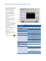
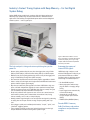
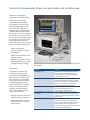
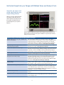
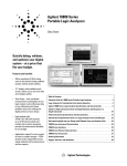
Agilent 16850 Series
Portable Logic Analyzers
Data Sheet
The industry’s fastest timing capture with deep
memory ― for fast digital system debug
• 2.5 GHz timing capture with
up to 128 M sample memory
for finding elusive problems
quickly, even far from the
trigger point
• Up to 1.4 GHz trigger
sequencer speed for state
and timing capture
• Single-ended and differential
probing for the widest range
of supported technologies
16850 Series Portable Logic Analyzer Selection Guide
• 80 ps resolution (12.5 GHz) Timing
Zoom with 256 K samples allows
you to observe signal timing in
proximity to the trigger point
• Up to 1.4 Gbps state data rate
tracks high speed parallel and
serial buses in your design
• Gain signal integrity insight on all
channels using exclusive
“eye scan”
• Four models with 34/68/102/136
channels provide the measurement flexibility for a wide range of
applications
• Application support for many
aspects of today’s complex designs
bring target insight FPGA dynamic
probe, and digital VSA (vector
signal analysis)
• Powerful, customizable triggering
quickly isolates problems
• Proven, easy to use interface
speeds debug
• Standard 15 inch touch screen
allows viewing of multiple buses
and signals
• Standard 3-year warranty
Specifications and
characteristics
Channels
Maximum timing sample rate
(half/full channel)
High-speed timing zoom
Trigger sequencer
Maximum state clock rate
Maximum state data rate
Maximum memory depth
Supported signal types
Automated threshold/sample
position
Simultaneous eye diagrams, all
channels
Probe compatibility
2
16851A 16852A 16853A 16854A
34
68
102
136
5 GHz (200 ps) with up to 256 M depth
2.5 GHz (400 ps) with up to 128M depth
12.5 GHz (80 ps) with 256 Kb depth
1.4 GHz
700 MHz with Option 700
350 MHz standard
1400 Mb/s with Option 700
700 Mb/s standard
2 M default
4 M with Option 004
8 M with Option 008
16 M with Option 016
32 M with Option 032
64 M with Option 064
128 M with Option 128
Single-ended, differential
Yes
Yes
Direct connect single-ended flying lead
Mictor and Soft Touch Pro connectorless
90-pin connector single-ended and differential
probes for flying lead, Mictor, Soft Touch, Soft
Touch Pro, and Samtec connections (used in
conjunction with a U4201A cable)
Select DDR2/3 BGA probes and probe cables
Select DDR3 Addr/Cmd slot interposer probes
Industry’s Fastest Timing Capture with Deep Memory ― for Fast Digital
System Debug
Agilent 16850 Series portable logic analyzers offer the highest performance,
with deep, high speed timing and state measurements, combined with the
applications and usability your digital development teams need to debug their
modern systems ― and at a great price.
Figure 1. With four models to choose
from, and options to upgrade state speed
and memory depth, you can get a logic
analyzer with measurement capabilities
that meet your needs.
The logic analyzer’s timing and state acquisition gives you the
power to:
Automate the capture of
internal FPGA signals
• Observe timing relationships far away from the trigger point using 2.5 GHz
(400 ps)/5 GHz (200 ps) full/half channel timing with up to 128 M samples
• Measure more precise timing relationships in the vicinity of the trigger point
using 12.5 GHz (80 ps) Timing Zoom (256 K samples)
• Find anomalies separated in time with memory depths upgradable to 128 M
• Probe a variety of technologies with single-ended and differential attachment
options with the highest signal integrity
• Buy what you need today and upgrade in the future. 16850 Series logic analyzers come with independent upgrades for state speed and memory depth
• Sample synchronous buses up to 1400 Mbps data rates accurately using eye
scan to automatically adjust threshold and setup/hold
• Easily track problems from symptom to root cause across several measurement modes by viewing time-correlated data in waveform/chart, listing,
inverse assembly, source code, or compare display
• Identify potential signal integrity issues on high data rate signals by observing
an analog view of all input channels via logic analyzer probing with “eye
scan”
• Set up triggers quickly and confidently with intuitive, “simple,” “quick,” and
“advanced” triggering options
• Time correlate and import oscilloscope/mixed-signal traces into the logic
analyzer Waveform window for even greater system insight
16850 Series logic analyzers, used
with the FPGA Dynamic Probe, let you
probe internal FPGA nets on Xilinx
and Altera devices with deep memory
and through an automated process
3
• No block RAM required
• Move probe points without stopping the FPGA or changing design
timing
• Import signal names automatically
from the FPGA design
• Automatically map FPGA pins
to logic analyzer input channels
(Xilinx)
• B4655A (Xilinx) B4656A (Altera)
Decode DDR2/3 memory
Addr/Cmd buses and perform
compliance and performance
analysis
Eye Scan to Set Sample Points and to View Signal Integrity
Automate measurement setup
and quickly gain diagnostic
clues
16850 Series logic analyzers make
it easy for you to get up and running
quickly by automating your measurement setup process. In addition, the
logic analyzer’s setup/hold window
(or sampling position) and threshold
voltage settings are automatically
determined so you can capture data
on high-speed buses with the highest
accuracy. Auto Threshold and Sample
Position mode allow you to...
• Obtain accurate and reliable measurements
• Save time during measurement
setup
• Gain diagnostic clues and identify
problem signals quickly
• Scan all signals and buses simultaneously or just a few
• View results as a composite display or as individual signals
• See skew between signals and
buses
• Find and fix inappropriate clock
thresholds
• Measure data valid windows
• Identify signal integrity problems
related to rise times, fall times,
data valid window widths
Figure 2. Eye scan automatically sets sample positions for accurate state capture
and also provides a signal integrity view of each input signal, without the need for an
oscilloscope.
Identify problem signals over one hundred channels simultaneously
As timing and voltage margins continue to shrink, confidence in signal integrity
becomes an increasingly vital requirement in the design validation process. Eye
scan lets you acquire signal integrity information on all the buses in your design,
under a wide variety of operating conditions, in a matter of minutes. Identify
problem signals quickly for further investigation with an oscilloscope. Results
can be viewed for each individual signal or as a composite of multiple signals or
buses.
4
16850 Series Logic Analyzer Specifications and Characteristics
Number of channels
16851A
34 (1 clock +
1 clock qualifier)
16852A
68 ( 1 clock +
3 clock qualifiers)
Deep timing (asynchronous) sampling mode
16853A
102 (1 clock +
3 clock qualifiers)
16854A
136 (1 clock +
3 clock qualifiers)
Conventional and transitional timing
(up to 128 M depth)
Maximum sample rate in full channel mode (nom)
Maximum sample rate in half channel mode (nom)
Sample period on all channels (nom)
Sample period in half channel mode (nom)
Minimum data pulse width (nom)
Maximum time between transitions (nom)
Time interval accuracy within a 16 channel pod (typ) 1
Time interval accuracy across 16 channel pods (typ) 1
2.5 GHz
5 GHz
400 ps to 10 ns
200 ps
1 sample period + 200 ps
66 days
± (1 sample period + 130 ps + 0.01% of time interval reading)
± (1 sample period + 400 ps + 0.01% of time interval reading)
1. With single-ended flying lead and Soft Touch Pro probes.
Timing zoom (captured simultaneously with timing or state sampling mode capture)
Timing analysis sample rate (nom)
Time interval accuracy (nom)
Within a 16 channel block
Between 16 channel blocks
Memory depth (nom)
Trigger position (nom)
Minimum data pulse width (nom)
12.5 GHz (80 ps sample resolution)
± (80 ps + 130 ps + 0.01% of time interval reading)
± (80 ps + 400 ps + 0.01% of time interval reading)
256 K samples
Start, center, end, or user-defined
1 sample period + 200 ps
State (synchronous) sampling mode
Maximum state data rate ― base (spec)
Maximum state data rate ― Option 700 (spec)
Maximum state clock frequency ― single edge clocking ― base (typ)
Maximum state clock frequency ― single edge clocking ― Option 700 (typ)
Minimum state clock frequency (typ) 1
Minimum data valid window (typ) 2
Sample position adjustment resolution (typ)
Sample position adjustment accuracy (typ)
Minimum data valid window (typ) 1
Minimum setup time (typ)
Minimum hold time (typ)
Minimum eye height (typ)
Sample position adjustment range (typ)
Minimum state clock pulse width single edge (typ)
Minimum time between active clock edges ― standard (typ)
Minimum time between active clock edges ― Option 700 (typ)
Maximum time between active clock edges (typ) 1
Clock qualifier setup time (typ)
Clock qualifier hold time (typ)
Time tag resolution (typ)
Maximum time count between stored states (nom)
1.
Clock can pause for up to 66 days once every 8 or more edges.
2.
Dependent on probing system.
5
700 Mb/s using both edges of clock (spec)
1.4 Gb/s using both edges of clock (spec)
350 MHz
700 MHz
12.5 MHz (single edge)
6.25 MHz (both edges)
160 ps
20 ps
± 150 ps
160 ps
80 ps
80 ps
160 mV
7 ns
200 ps
1429 ps
714 ps
80 ns (single edge)
200 ps
200 ps
80 ps
66 days
16850 Series Logic Analyzer Specifications and Characteristics (continued)
Trigger characteristics (conventional timing, transitional timing, and state sampling modes)
Maximum trigger sequence speed (standard) (nom)
Maximum trigger sequence speed (option 700) (nom)
Maximum trigger sequence levels (nom)
Trigger sequence level branching (nom)
Trigger position (nom)
Trigger resources (nom)
Maximum occurrence counter (nom)
Maximum pattern width (nom)
Maximum range width (nom)
Timers range (nom)
Timer resolution (nom)
Timer accuracy (typ)
Timer reset latency (nom)
700 MHz (state), 1.4 GHz (timing)
1.4 GHz
8
Arbitrary 4-way if/then/else
Start, center, end or user-defined
16 patterns evaluated as =, !=, >, >=, <, <=
8 double-bounded ranges evaluated as in range, not in range
4 edge detectors in timing, 3 in transitional timing
1 occurrence counter per sequence level
1 timer
3 flags
1 arm in
Arbitrary Boolean combinations
Go To
Trigger and fill memory
Trigger and Go To
Trigger, send e-mail, and fill memory
Occurrence counter reset
Default (global) and per sequence level
Store/don’t store sample
Turn on/off default storing
Start from reset
Stop and reset
Pause
Resume
Set
Clear
Pulse set
Pulse clear
999,999,999
128 bits – single label
64 bits
200 * sample clock period to 27 hours
5 ns
± (8 * sample clock period + 2ns + 0.01%)
80 * sample clock period
Input signal amplitude Vamptd (typ)
Supported signal types
Voltage threshold (typ)
Threshold resolution (typ)
Threshold accuracy (typ)
Threshold setting granularity
≥ 350 mV
Single-ended and differential
–5 V to +5 V
2 mV
± (30 mV + 1% of setting)
Individual threshold for each channel
Trigger resource Boolean conditions (nom)
Trigger actions (nom)
Store qualification actions (nom)
Timer actions
Flag actions
General
1. Specification (spec): Represents warranted performance of a calibrated instrument that has been stored for a minimum of 2 hours
within the operating temperature range of 0 to 40 °C, unless otherwise stated, and after a 45-minute warm-up period. The specifications include measurement uncertainty.
2. Typical (typ): Represents characteristic performance, which 80% of the instruments manufactured will meet. This data is not warranted, does not include measurement uncertainty, and is valid only at room temperature (approximately 25 °C).
3. Nominal (nom): The expected mean or average performance, or an attribute whose performance is by design, such as the 50 Ω
connector. This data is not warranted and is measured at room temperature (approximately 25 °C).
4. Measured (meas): An attribute measured during the design phase for purposes of communicating expected performance, such as
amplitude drift versus time. This data is not warranted and is measured at room temperature (approximately
25 °C).
6
Unleash the Complementary Power of a Logic Analyzer and an Oscilloscope
Seamless oscilloscope
integration with View Scope
Easily make time-correlated
measurements between Agilent
logic analyzers and oscilloscopes.
The time-correlated logic analyzer
and oscilloscope waveforms are
integrated into a single logic analyzer
waveform display for easy viewing
and analysis. You can also trigger the
oscilloscope from the logic analyzer
(or vice versa), automatically de-skew
the waveforms and maintain marker
tracking between the two instruments. View Scope allows you to perform the following more effectively:
• Validate signal integrity
• Track down problems caused by
signal integrity
• Validate correct operation of A/D
and D/A converters
• Validate correct logical and timing
relationships between the analog
and digital portions of a design
Connection
The Agilent logic analyzer and
oscilloscope can be physically
connected with standard BNC and
LAN connections. Two BNC cables
are connected for cross triggering,
and the LAN connection is used to
transfer data between the instruments. The View Scope correlation
software is standard in the logic
analyzer’s application software
version 3.50 or higher. The View
Scope software includes:
• Ability to import some or all of the
captured oscilloscope waveforms
• Auto scaling of the scope waveforms for the best fit in the logic
analyzer display
Figure 3. View Scope seamlessly integrates your scope and logic analyzer waveforms into
a single display.
Feature
Benefit
Automated setup
Integrated waveform display
Automatic measurement de-skew
Cross trigger the logic analyzer and
oscilloscope
Tracking markers
7
Quickly get to your first measurement using
the logic analyzer’s Help wizard for easy
setup, regardless of which supported Agilent
oscilloscope you connect to.
Instantly validate the logical and timing
relationships between the analog and digital
portions of your design. View oscilloscope and
logic analyzer waveforms integrated into a
single logic analyzer waveform display.
Save time and gain confidence in measurement
results with measurements that are
automatically de-skewed in time.
Start your debug approach from either the
analog or digital domain with the flexibility to
trigger the oscilloscope from the logic analyzer
(or vice versa).
Precisely relate information on the
oscilloscope’s display to the corresponding
point in time on the logic analyzer display with
tracking markers. The oscilloscope’s time
markers automatically track adjustments of the
logic analyzer’s global markers.
Get Instant Insight into your Design with Multiple Views and Analysis Tools
Acquisition and analysis tools
provide rapid insight into your
toughest debug problems
When you want to understand what
your target is doing and why, you
need acquisition and analysis tools
that rapidly consolidate data and
provide insight into your system’s
behavior.
Figure 4. Perform in-depth time, frequency and modulation domain analysis on your
digital baseband and IF signals with Agilent’s 89600 Vector Signal Analysis software,
running on the logic analyzer.
Optional analysis and automated measurement packages
B4655A FPGA Dynamic Probe (Xilinx), B4656A FPGA
Dynamic Probe (Altera)
Gain unprecedented visibility into your FPGA’s internal activity. Make
incremental real-time measurements in seconds without stopping the FPGA,
changing the design or modifying design timing. Quickly set up the logic
analyzer with automatic pin mapping and signal bus naming by leveraging
work you did in your design environment. www.agilent.com/find/fpga
89601B-300 digital vector signal analysis, hardware
Perform time-domain, spectrum, and modulation quality analysis on digital
connectivity for logic analyzers
Baseband and IF signals. www.agilent.com/find/dvsa
B4601C serial-to-parallel analysis package
Eliminate the tedious, time-consuming, and error-prone task of sifting through
thousands of analysis package serial bits by looking at long vertical columns
of captured 1’s and 0’s. The B4601C serial-to-parallel analysis package is
general-purpose software that allows easy viewing and analysis of serial data.
B4602A signal extractor tool
This tool processes input signals and based on xml algorithms and creates a
mapping of captured signals into new bus and signal names
B4606A advanced customization environment—
Tailor your logic analyzer interface with a wide range of control, analysis
development and runtime package
and display capabilities specific to your measurement application. Create
integrated dialogs, graphical displays and analysis functions to quickly
manipulate measurement data into a format that provides additional insight
and answers. www.agilent.com/find/logic-customview
B4607A advanced customization environment—
Run the macros and graphical views created with a B4606A development
runtime package
package or obtain and run a variety of commonly requested tools from Agilent
and its partners to help customize your measurement environment.
B4608A ASCII remote programming interface
Remotely control a 16850-Series logic analysis system by issuing ASCII
commands. This interface is designed to be as similar as possible to the RPI
on the 16700 Series logic analysis system, so that you can reuse existing
programs. Requires either B4606A or B4607A to be enabled. You can also use
the B4606A to customize and add RPI commands.
B4610A data import package
Use the logic analyzer GUI to view data obtained from tools other than a logic
analyzer.
B4630A MATLAB® connectivity and analysis package Make an easy connection to MATLAB and transfer your logic analyzer
measurement data for processing. Display the results on the logic analyzer in
an XY scattergram chart.
8
Validate your DDR2 and DDR3 Memory Systems
The state analysis capabilities of the 16850 Series allow it to make measurements and analysis on DDR2 and DDR3 memories up to
DDR2/3 1333 (667 MHz clock) on address and control lines. Memory bus decode, compliance testing, and performance analysis are
available in state mode only with related orderable tools.
Addr/Cmd only
DDR2 memory
DDR3 memory
Up to DDR2 1333 (667 MHz clock) state measurements
on Addr/Cmd only. (No Data)
Up to DDR3 1333 (667 MHz clock) state measurements
on Addr/Cmd only. (No Data)
Requires 34 channel model or higher (one U4201A cable required providing two 90 pin pods)
Related Orderable SW Tools (State mode only):
• B4621B Bus Decoder for DDR, DDR2, DDR3, DDR4 Debug and Validation (Only DDR2 and DDR3 are supported
with the 16850 Series logic analyzer.)
• B4622B Protocol Compliance and Analysis Toolset for DDR/2/3/4, and LPDDR/2/3 (Only DDR2 and DDR3 are
supported with the 16850 Series logic analyzer.)
Supported probes with configuration files:
Supported probes with configuration files:
• x16 Addr/Cmd/Data DDR2 BGA probe (W2631B)
(Requires E5384A ZIF probe) 1
• x16 Addr/Cmd/Data DDR3 BGA probe (W3631A)
(Requires E5845A ZIF probe) 1
• x8 Addr/Cmd/Data DDR2 BGA probe (W2633B)
(Requires E5384A ZIF probe) 1
• x8 Addr/Cmd/Data DDR3 BGA probe (W3633A)
(Requires E5847A ZIF probe) 1
FS2372 DDR3 DIMM interposer (Addr/Cmd only)
FS2374 DDR3 SODIMM interposer (Addr/Cmd only)
Addr/Cmd/Data Up to DDR2 800 (400 MHz clock) timing measurements
using 2.5 GHz timing analyzer with deep memory
(for 3:1 ratio of sample rate to data rate)
Up to DDR3 800 (400 MHz clock) timing measurements
using 2.5 GHz timing analyzer with deep memory
(for 3:1 ratio of sample rate to data rate)
Requires 68 channel model or higher (two U4201A cables using three of the four 90 pin pods provided)
Supported probes with configuration files:
Supported probes with configuration files:
• x16 Addr/Cmd/Data DDR2 BGA probe (W2631B)
(Requires E5384A ZIF probe)
• x16 Addr/Cmd/Data DDR3 BGA probe (W3631A)
(Requires E5845A ZIF probe)
• x8 Addr/Cmd/Data DDR2 BGA probe (W2633B)
(Requires E5384A ZIF probe)
• x8 Addr/Cmd/Data DDR3 BGA probe (W3633A)
(Requires E5847A ZIF probe)
For higher speed memory analysis or greater channel count refer to the U4154A logic analyzer module.
1. Data pod is not connected for State measurements when used with the 16850 Series. Simultaneous State mode capture of Read and
Write data requires a U4154A high-performance logic analyzer module with dual sample mode.
9
Validate your DDR2 and DDR3 Memory Systems (continued)
16850 Series capture and decode of DDR3 Addr/Cmd lines
Performance test analysis of DDR3 Addr/Cmd line saved trace
Compliance test analysis of DDR3 Addr/Cmd line saved trace
Figure 5. Multiple views for DDR2 and DDR3 Addr/Cmd capture.
10
Deep memory capture with 2.5 GHz (400 ps resolution) timing
Figure 6. Timing mode capture with
400 ps resolution and up to 128 M
samples memory depth (example capture
at –500 μs before trigger).
Powerful, customizable triggering with a 1.4 GHz sequencer
Figure 7. Example of a time out trigger to
capture an error condition.
11
16850 Series Instrument Characteristics
Standard data views
Waveform
Listing
Compare
Source code
Eye scan
Data display
Numeric bases for data display
Integrated display of data as digital waveforms, analog waveforms imported from an
external oscilloscope, and/or as a chart of a bus’ values over time
Displays data as a state listing
Compares data from different acquisitions and highlights differences
Displays time-correlated source code and inverse assembly simultaneously in a split display
Define the trigger event by simply clicking on a line of source code
Obtain source-code-level views of dynamically loaded software or code moved from ROM to
RAM during a boot-up sequence using address offsets
Requires access to source files via the LAN or instrument hard drive to provide source code
correlation
Source correlation does not require any modification or recompilation of your source code
Displays eye diagrams across all buses and signals simultaneously, allowing you to identify
problem signals quickly
Binary, hex, octal, decimal, signed decimal (two’s complement), ASCII, symbols, and
processor mnemonics
Symbolic support/object file format compatibility
Number of symbols/ranges
Object file formats supported
ASCII
User defined symbols
Available data/file formats
ala
xml
csv
mfb
Standard analysis tools
Filter/colorize
Find (next/previous)
Unlimited (limited only by amount of virtual memory available on 16850 Series logic
analyzers)
IEEE-695, Aout, Omf86, Omf96, Omf386, Sysrof, ELF/DWARF1 1, ELF/DWARF2 1, ELF/
Stabs1, ELF/Stabs2, ELF/Mdebug Stabs, TICOFF/COFF, TICOFF/Stabs
GPA (general purpose ASCII)
Specify a mnemonic for a given bit pattern for a label or bus
Contains information to reconstruct the display appearance, instrument settings, and trace
data (optional) that were present when the file was created
Extensible markup language for configuration portability and programmability
CSV (comma-separated values) format for transferring data to other applications like
Microsoft® Excel
Export logic analyzer data for post-processing. Mfb data can be parsed using programming
tools
Show, hide, or color certain samples in a trace for easier identification and analysis
Locate specific data in a captured trace
12
16850 Series Instrument Characteristics (continued)
16850 Series PC characteristics
Operating system
Processor
Chipset
System memory
Removable Hard disk drive
Installed on hard drive
Microsoft Windows® 7 Embedded (64-bit)
Core 2 Duo, M890, 3.0 GHz microprocessor
Intel Q45
4 GB
500 GB
Operating system, latest revision of the logic and protocol application software, optional
application software ordered with the logic analyzer
16850 Series instrument controls
LCD touch-screen display
Front-panel hot keys
Front-panel knob
Keyboard and mouse
Large 38.1-cm (15-in.) touch-screen display makes is easy to view a large number of waveforms
or states
Dedicated hot keys for selecting run mode and disabling touch screen
General-purpose knob adjusts viewing and measurement parameters
PS/2 keyboard and USB mouse
16850 Series video display modes
Touch-screen display standard
External display
Size
Resolution
Simultaneous display capability
38.1 cm (15 in.) diagonal
1024 x 768
Front panel and external display can be used
simultaneously at 1024 x 768 resolution
Supports up to four external monitors at up to 1600 x 1200 (with PCI video card)
Programmability
You can write programs to control the logic analyzer application from remote computers on the local area network using
COM or ASCII.
The COM automation server is part of the logic analyzer application. This software allows you to write programs to control
the logic analyzer. All measurement functionality is controllable via the COM interface.
The B4608A Remote Programming Interface (RPI) lets you remotely control a 16850 Series logic analyzer by issuing ASCII
commands to the TCP socket on port 6500. This interface is designed to be as similar as possible to the RPI on 16700
Series logic analysis systems, so that you can reuse existing programs.
The remote programming interface works through the COM automation objects, methods, and properties provided for
controlling the logic analyzer application. RPI commands are implemented as Visual Basic modules that execute COM
automation commands, translate their results, and return proper values for the RPI. You can use the B4606A advanced
customization environment to customize and add RPI commands.
Logic analyzer
(16850/16800/16900)
or PC running Agilent
logic analyzer application
Computer with
Windows XP or
Windows 7
Figure 8. 16850 Series programming
overview.
Distributed COM
13
LAN connection
Instrument COM
automation server
16850 Series Interfaces
Peripheral interfaces
Display
Keyboard
Mouse
Serial
PCI card expansion slot
Audio ports
USB
One 15-pin XGA connector and one DVI connector
PS/2
PS/2
9-pin D-sub
1 full profile
Line in, line out, mic in
Six 2.0 ports, two in front, four in rear
LAN
Connector
10Base-T, 100Base-T, 1000Base-T
RJ-45
Connectivity interfaces
Interface with external instrumentation
Trigger or arm external devices or receive signals that can be used to arm measurement hardware within the logic analyzer with
Trigger In/Out
Trigger in
Input
Action taken
Input signal level
Threshold level
Minimum signal amplitude
Connector
Input resistance
Trigger out
Trigger
Output signal
Threshold level
Signal load
Connector
Rising edge or falling edge
When received, the logic analyzer takes the actions described in the trigger sequence step
± 5 V max
Selectable: ECL, LVPECL, LVTTL, PECL, TTL
User defined (± 5 V in 50 mV increments)
200 mV
BNC
4 kΩ nominal
Rising edge or falling edge. OR of selected events that cause Trigger Out (logic analyzer
trigger or flags)
VOH (output high level) 2.0 V min
VOL (output low level) 0.5 V max
Pulse width approx. 80 to 160 ns
LVTTL (3.3 V logic)
50 Ω (For good signal quality, the trigger out signal should be terminated in 50 Ω to ground)
BNC
14
16850 Series Physical Characteristics
Power
16851A
16852A
16853A
16854A
Add 1.25 inches to the
width to account for
probes that plug into the
right side of instrument
443.23
(17.45)
Dimensions
100 to 240V ± 10 %,
50/60Hz, 400 W max
100 to 240V ± 10 %,
50/60Hz, 400 W max
100 to 240V ± 10 %,
50/60Hz, 400 W max
100 to 240V ± 10 %,
50/60Hz, 400 W max
292.2
(11.53)
Note:
• The mains supply voltage fluctuations are not to exceed ± 10 % of the
nominal supply voltage.
• Add 1.25 inches to the width to
account for probes that plug into the
right side of instrument.
Dimensions: mm
(in)
456.8
(17.98)
Figure 9. 16850 Series exterior dimensions.
Weight Max net
16851A
16852A
16853A
16854A
15.0 kg
(33.0 lbs)
15.0 kg
(33.0 lbs)
15.0 kg
(33.0 lbs)
15.0 kg
(33.0 lbs)
Max
shipping
21.7 kg
(48 lbs)
21.7 kg
(48 lbs)
21.7 kg
(48 lbs)
21.7 kg
(48 lbs)
15 inch built-in
color LCD display,
touch screen
standard
General purpose knob
Run/stop keys
On/Off power switch
USB ports
Touch screen on/off
AC power
Trigger in
Trigger out
Mouse
Clock in
Keyboard
10/100/1000 Base-T LAN
Serial port
2.0 USB ports (4)
Audio ports
External display ports
Figure 10. 16850 Series front and back panels.
Instrument operating
environment
Temperature
Altitude
Humidity
5 °C to 40 °C
(41 °F to 104 °F)
To 2000 m (6,561 ft)
Maximum 80% relative
humidity, noncondensing
Probe inputs
Figure 11. 16850 Series side view.
Extra notes regarding the 16850
Series:
1. Pollution degree 2;
2. Installation category II;
3. These instruments are intended
for use in an indoor lab
environment
15
Ordering Information
Each 16850 Series portable logic analyzer comes with one USB keyboard, one USB mouse, accessory pouch, power cord
and 3-year warranty standard.
Selecting a logic analyzer to meet your application and budget is as easy as 1, 2, 3.
Choose the channel count
Model
16851A
1
Channels
2
34
16853A
68
102
16854A
136
Choose the state speed
State speeds
3
16852A
350 MHz state clock; 700 Mbps data rate: Standard
700 MHz state clock; 1.4 Gbps data rate: < Model number > -700
Choose the memory depth
Memory depth (samples)
2 Mb: Standard
4 Mb: < Model number > -004
8 Mb: < Model number > -008
16 Mb: < Model number > -016
32 Mb: < Model number > -032
64 Mb: < Model number > -064
128 Mb: < Model number > -128
16850 Series Probing Options
Logic analyzer probes are ordered separately. Please specify probes when ordering to ensure the correct connection
between your logic analyzer and the device under test.
16850 Series logic analyzer probes
General-purpose flying lead probes
U4203A
E5381A
E5382A
34-ch single-ended data, differential clock, direct connect
17-ch differential probe for 90 pin LA pod 1, 2
17-ch single-ended probe for 90 pin LA pod 1, 2
E5387A
E5398A
E5390A
E5405A
E5406A
Soft Touch Classic Series: 17-ch differential for 90 pin LA pod 1, 2
Half-Size Soft Touch: 17-ch single-ended for 90 pin LA pod 1, 2
Soft Touch Classic Series: 34-ch single-ended for 90 pin LA pod 1, 3
Soft Touch Pro Series: 17-ch differential for 90 pin LA pod 1, 2
Soft Touch Pro Series: 34-ch single-ended for 90 pin LA pod 1, 3
U4201A
U4205A
E5378A
E5379A
E5380A
34-ch logic analyzer cable for use with E5xxxA 90-pin probes
Mictor: 34-ch single-ended data and clock, direct connect
Samtec: 34-ch single-ended probe for 90 pin LA pod 1, 3
Samtec: 17-ch differential probe for 90 pin LA pod 1, 2
Mictor: 34-ch single-ended probe for 90 pin LA pod 1, 2
Connectorless probes
Connector probes
1. Logic analyzer probe used with the U4201A logic analyzer cables.
2. 17 channel probes require one of two 90 pin pods provided on the U4201A logic analyzer direct connect cable.
3. 34 channel probes require both 90 pin pods provided on the U4201A logic analyzer cable.
16
Additional 16850 Series Options
Agilent product or option number Description
E5864A
Additional external hard drive (imaged
with operating system and logic analyzer
application software)
Ordering information
E5864A
After Purchase Options
Upgrade memory depth or state speed after purchase
Logic analyzer channels
Logic analyzer models
After purchase upgrade model numbers
Memory depth (samples)
State speed
34
16851A
16851AU
68
102
136
16852A
16853A
16854A
16852AU
16853AU
16854AU
4 M: < Upgrade model number > -004
8 M: < Upgrade model number > -008
16 M: < Upgrade model number > -016
32 M: < Upgrade model number > -032
64 M: < Upgrade model number > -064
128 M: < Upgrade model number > -128
700 MHz state clock/1400 Mbps state data rate: < Upgrade model number > -700
Related Literature
Publication title
Publication type
Agilent Technologies 16850 Series Logic Analyzers
Agilent Technologies 16900 Series Logic Analysis Systems
Agilent Technologies Measurement Modules for the 16900 Series
B4655A FPGA Dynamic Probe for Xilinx - Data Sheet
Probing Solutions for Logic Analyzers - Data Sheet
Flyer
Color brochure
Data sheet
Data sheet
Data sheet
17
Publication number
5991-2836EN
5989-0420EN
5989-0422EN
5989-0423EN
5968-4632E
www.agilent.com
www.agilent.com/find/16850-Series
myAgilent
myAgilent
www.agilent.com/find/myagilent
A personalized view into the information most
relevant to you.
www.axiestandard.org
AdvancedTCA® Extensions for
Instrumentation and Test (AXIe) is an
open standard that extends the
AdvancedTCA for general purpose and
semiconductor test. Agilent is a founding
member of the AXIe consortium.
Three-Year Warranty
www.agilent.com/find/ThreeYearWarranty
Agilent’s combination of product reliability
and three-year warranty coverage is another
way we help you achieve your business goals:
increased confidence in uptime, reduced cost
of ownership and greater convenience.
Agilent Advantage Services
www.agilent.com/find/AdvantageServices
Accurate measurements throughout the
life of your instruments.
DEKRA Certified
ISO 9001:2008
Agilent Electronic Measurement Group
www.lxistandard.org
LAN extensions for Instruments puts the
power of Ethernet and the Web inside
your test systems. Agilent is a founding
member of the LXI consortium.
www.pxisa.org
PCI extensions for Instrumentation
(PXI) modular instrumentation delivers
a rugged, PC-based high-performance
measurement and automation system.
Agilent Channel Partners
www.agilent.com/find/channelpartners
Get the best of both worlds: Agilent’s
measurement expertise and product
breadth, combined with channel partner
convenience.
MATLAB® is a U.S. registered trademark of
Math Works, Inc.
Intel is a U.S. registered trademark of Intel
Corporation.
®
PCI Express® and PCI-X® are registered trademarks of PCI-SIG.
Quality Management System
Sys
www.agilent.com/quality
For more information on Agilent
Technologies’ products, applications or
services, please contact your local Agilent
office. The complete list is available at:
www.agilent.com/find/contactus
Americas
Canada
Brazil Mexico
United States
(877) 894 4414
(11) 4197 3600
01800 5064 800
(800) 829 4444
Asia Pacific
Australia 1 800 629 485
China
800 810 0189
Hong Kong 800 938 693
India 1 800 112 929
Japan
0120 (421) 345
Korea
080 769 0800
Malaysia 1 800 888 848
Singapore 1 800 375 8100
Taiwan
0800 047 866
Other AP Countries (65) 375 8100
Europe & Middle East
Belgium 32 (0) 2 404 93 40
Denmark
45 45 80 12 15
Finland
358 (0) 10 855 2100
France
0825 010 700*
*0.125 €/minute
Germany
49 (0) 7031 464 6333
Ireland
1890 924 204
Israel972-3-9288-504/544
Italy
39 02 92 60 8484
Netherlands
31 (0) 20 547 2111
Spain
34 (91) 631 3300
Sweden
0200-88 22 55
United Kingdom 44 (0) 118 927 6201
For other unlisted countries:
www.agilent.com/find/contactus
(BP-3-1-13)
Product specifications and descriptions
in this document subject to change
without notice.
© Agilent Technologies, Inc. 2013
Published in USA, September 24, 2013
5991-2791EN