1
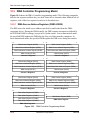
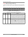
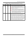
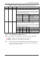
Chapter 10
DMA Controller
Direct Memory Access (DMA) is one of several methods for coordinating the timing of
data transfers between an input/output (I/O) device and the core processing unit or
memory in a computer. DMA is one of the faster types of synchronization mechanisms,
generally providing significant improvement over interrupts, in terms of both latency and
throughput. An I/O device often operates at a much slower speed than the core.1 DMA
allows the I/O device to access the memory directly, without using the core. DMA can
lead to a significant improvement in performance because data movement is one of the
most common operations performed in processing applications. There are several
advantages of using DMA, rather than the core, in the DSP56300 family:
■
DMA saves core MIPS because the core can operate in parallel.
■
DMA saves power because it requires less circuitry than the core to move data.
■
DMA saves pointers because core AGU pointer registers are not needed.
■
DMA has no modulo block size restrictions, unlike the core AGU.
Traditionally, DMA uses the same internal address and data buses as the core.
Consequently, when DMA performs one or more word transfers, it can cause the core to
temporarily halt activity for one or more cycles while DMA moves the data. With this
type of architecture, the core and DMA cannot both perform data moves in the same core
clock cycle. To overcome data movement restrictions imposed by sharing resources with
the core, the DMA system in the DSP56300 family contains its own dedicated internal
address and data buses. Internal memory is partitioned so that the Program Control Unit
(PCU) and DMA can both perform internal memory accesses in the same core clock
cycle, as long they are accessing different memory partitions. Also, if one of these two
controllers (PCU or DMA) is accessing internal memory, the other controller can perform
an external memory access in the same core clock cycle.
1. The term “core” has a special meaning when described in the context of DMA. Technically, the
DSP56300 core contains all of the circuitry that is common to all devices in the DSP56300 family,
including the DMA controller and buses. However, when described in the context of DMA, the core
actions referred to are those caused by data movement instructions executed by the PCU, not data movement performed by DMA.
Motorola
DSP56300 Family Manual
10-1
In addition to data moves between I/O and internal or external memory, the DMA in the
DSP56300 can perform memory-to-memory transfers (internal, external, or mixed). Table
10-1 summarizes by source/destination type the various types of data transfers that the
DMA Controller can perform.
Table 10-1 DMA Controller Data Transfers
Clock Cycles per Single Word Transfer1
Type of Transfer
Internal Memory
→
Internal Memory
2
External Memory
↔
Internal Memory
2 + wait states
External Memory
→
External Memory2
2 + wait states
Internal Memory
↔
Internal I/O
2
External Memory
↔
Internal I/O
2 + wait states
Internal I/O
→
Internal I/O
2
NOTES:
1. Data transfer for one channel takes a minimum of two clock cycles per single word.
2. External memory includes external I/O.
The DMA unit contains the necessary counters, offset registers, and pointers to
transparently handle one-, two-, and three-dimensional data matrix transfers. These
registers can be given values that result in special addressing modes, for example, access
to circular buffers and linear buffers with non-unit stride. The data structure
dimensionality can be chosen independently for the source access versus the destination
access involved in the data move. The DSP56300 contains six DMA channels that share
buses and offset registers but are otherwise independent. Each DMA channel can be
triggered by interrupt pins, peripheral actions, or other DMA events, and assigned a
priority relative to other channels and relative to the core. Each of the six DMA channels
contains its own set of four operational registers, all of which are memory-mapped in the
internal I/O memory space and all of which are 24-bit registers:
■
DMA Source Address Register (DSR): A read/write register that contains the source
address for the next DMA transfer for its channel. Each DMA channel has one
DSR: DSR0, DSR1, DSR2, DSR3, DSR4 and DSR5.
■
DMA Destination Address Register (DDR): A read/write register that contains the
destination address for the next DMA transfer for its channel. Each DMA channel
has one DDR: DDR0, DDR1, DDR2, DDR3, DDR4 and DDR5.
■
DMA Counter (DCO): A read/write register that contains the number of DMA data
transfers to be performed by its channel. The DCO has five modes of operation
determined by the DMA channel Address Generation mode defined in the DMA
channel’s Control Register. Each DMA channel has one DCO: DCO0, DCO1,
DCO2, DCO3, DCO4 and DCO5.
10-2
DSP56300 Family Manual
Motorola
DMA Operational Overview
■
DMA Control Register (DCR): A read/write register that controls the operation of a
DMA channel. Each DMA channel has one DCR: DCR0, DCR1, DCR2, DCR3,
DCR4 and DCR5.
The DMA Controller also has supporting 24-bit registers available to all the DMA
channels:
■
DMA Offset Register (DOR): Each DOR is a read/write register that contains the
offset value to be used in some of the DMA addressing modes. The DMA
controller has four common offset registers (DOR0, DOR1, DOR2 and DOR3) that
can be used by all the channels according to their Address Generation mode.
■
DMA Status Register (DSTR): This read-only register reflects the overall operating
status of all channels in the DMA Controller.
In summary, the DSP56300 DMA can perform I/O and memory accesses that are
independent of and frequently simultaneous with PCU operations. DMA can transfer
memory-to-memory and handle mixed multi-dimensional and special address mode
transfers. DMA contains six highly independent channels with separate priorities and
multiple trigger choices. These capabilities significantly enhance code performance.
10.1 DMA Operational Overview
The following subsections describe how the DSP56300 DMA operates. These subsections
are organized by function, rather than by event sequence. The DMA register description
section contains detailed operational information.
10.1.1 Basic Address Modes
The DSP56300 DMA can deal with the following basic types of data structures:
■
Constant Addressing: This mode uses a single address throughout the data transfer.
Typically this is used by I/O devices that use a single address to transfer
information.
■
One-dimensional: A one-dimensional matrix consisting of one item or a “line” of
items located in consecutive memory locations.
■
Two-dimensional: A two-dimensional matrix or table that is stored in row-column
order with equal spacing in memory between each row or line.
■
Three-dimensional: A three-dimensional matrix or collection of tables that are
equally spaced in memory.
The type of data structure is specified in the counter mode for the DMA channel. The
counter mode divides a given 24-bit counter register into one or more sections, one for
Motorola
DMA Controller
10-3
DMA Operational Overview
each dimension used. The appropriate counter fields either decrement or reload each time
the DMA transfers a data word. A counter field is reloaded with its initial value after that
field is decremented to zero. For details on counter operation, see Section 10.5.3, "DMA
Counters (DCO[5 – 0])," on page 10-11. Once all fields in the counter are exhausted, one
or more data moves are performed and all words, lines, and tables are transferred. The
total collection of data moved is called the “block.” Exhaustion of the entire counter
results in a single “block transfer.” The automatic counter register updates are directly
performed on the user-visible counter register. In other words, the counter register is used
for both the count load/reload function and the count decrement function.
10.1.2 Special Address Modes
The counter and offset registers can be loaded with special values to produce variants of
the basic addressing modes. Some examples covered in more detail in later sections
include:
■
Circular buffer: Use a two-dimensional counter and a negative offset that wraps
back to the buffer start address.
■
Linear buffer with non-unit stride: Use a two-dimensional counter with one word
per row. This method must be used with byte packing, which has a stride of three.
■
A larger-than-normal field width in a two-dimensional counter: Concatenate two
fields in a three-dimensional counter by specifying an offset value of one between
them.
10.1.3 Unmatched Source and Destination Dimensions
The source and destination data structures can have different dimensions.2 The data
structure with the largest dimension is read or written once during the block transfer; the
data structure with the smaller dimension can be written or read repeatedly. For this
situation, a single counter register handles both sides of the transfer. The high-dimension
(three-dimensional or two-dimensional) side of the transfer determines the counter mode
and thus the number of available counter fields. Each “tick” of the counter counts one
word transfer; that is, one source read and one destination write.
The data structure on the low-dimension side of the transfer is fully described by a
right-justified subset of the counter—the number of counter fields being the same as its
dimension (two-dimensional or one-dimensional). This data structure access is repeated
(using the exact same addressing sequence) the number of times specified by the upper
2. For an example, see the Motorola application report, APR/23, Using the DSP56300 Direct Memory
Access Controller.
10-4
DSP56300 Family Manual
Motorola
DMA Operational Overview
field(s) of the counter. The pointer wraparound back to the beginning of this data structure
is accomplished using a negative offset register value, similar to a circular buffer.
10.1.4 DMA Triggers (Request Sources)
Data movement in by a particular DMA channel is initiated by either a hardware or a
software trigger. Following is an example list of some of the hardware and software DMA
triggers, also known as DMA request sources. Peripheral triggers are device-dependent. A
DMA channel can be configured for triggering by only one source at a time.
■
Hardware triggers
— External interrupt pins (IRQA - IRQD)
— DMA channel block transfer completion (by this or a different DMA channel)
— Peripheral status bits
— Receiver has new datum to be read by DMA
— Transmitter needs new datum from DMA to send
— Timer compare event
■
Software triggers
— DMA Enable bit for this DMA channel
A peripheral status bit that triggers an enabled DMA transfer also typically can trigger an
enabled peripheral interrupt. The DMA transfer is triggered by the status bit change, not
by the peripheral interrupt event, and the DMA transfer occurs whether or not the
peripheral interrupt is enabled. Furthermore, avoid triggering a DMA transfer and a
peripheral interrupt from the same event; this can result in a lack of coordination regarding
resources and status bit changes.
10.1.5 Transfer Mode
When a DMA channel is enabled and receives a trigger from its configured trigger source,
it begins moving data as soon as the needed resources become available (for example,
internal DMA buses and memory locations). As a result of the trigger event, the channel
transfers either all or a subset of the block (this is configurable). The amount of data that is
transferred in response to each trigger event is determined by the DMA transfer mode.
Besides the trigger data structure, the transfer mode also selects either a hardware or
software trigger, and automatic block repeat enable. The available transfer modes are
single word, line, and block. Typically, a DMA channel used in conjunction with a
peripheral operates in a single word transfer mode (triggered by a receiver full or
transmitter empty condition).
Motorola
DMA Controller
10-5
Timing (Core Clock Cycles)
10.2 Timing (Core Clock Cycles)
This section describes the timing of core and DMA data transfers in the context of integral
core clock cycle counts. When the needed resources are available, each word transfer
performed by the DMA takes at least two core clock cycles:
■
Source read (at least one cycle)
■
Destination write (at least one cycle)
Any wait states incurred during external memory accesses are added to the DMA word
transfer time (for external source and/or destination).
Some peripherals (generally those using first-in-first-out (FIFO) for data transfer) may act
as “fast DMA request sources.” These peripherals can trigger a new DMA request as often
as every two core clock cycles, thereby using the DMA at its maximum throughput rate
with zero overhead time.
10.2.1 Non-Overlap Between DMA Channels
Data movement can never be performed by more than one DMA channel within a given
core clock cycle. For example, it is not possible for Channel 1 to commence its source
read before Channel 0 completes its destination write. This non-overlap limitation exists
for all situations, including the following cases:
■
One channel needs to read (write) from external memory, and another channel
needs to write (read) to internal memory.
■
One of the DMA channels is waiting on the Bus Interface Unit (BIU) for an
external access to complete, and the BIU is in turn waiting because of:
— Static wait states (determined by Bus Control Register)
— Dynamic wait states (controlled by TA pin)
— Byte packing
This limitation is necessary because there is only one internal DMA address bus and one
internal DMA data bus. The internal DMA buses are in use by a DMA channel even
during the external memory access phase of the DMA word transfer. Although channel
overlap during DMA channel transfers cannot exist, zero overhead between two DMA
channel transfers can exist. Once the word transfer performed by a DMA channel is
completed, another DMA channel can begin data movement in the very next core clock
cycle—if the second DMA channel has already been triggered and is not being delayed by
contention or priority issues.
10-6
DSP56300 Family Manual
Motorola
Channel Priority
10.2.2 Overlap between DMA Channel and Core
Since the core and DMA use separate address and data buses, both can perform data
movement in a given core clock cycle. This overlap of data movement can occur for the
following cases:
■
The core is accessing internal memory while DMA is accessing a different internal
memory partition:
— RAM: 1/4 Kword partition size (this size is device-dependent)
— ROM: 2, 3, or 4 Kword device-specific partition size
If the core and DMA try to access the same internal memory partition, the core has
priority and DMA is delayed.
■
The core is accessing internal (external) memory while DMA is accessing external
(internal) memory
10.3 Channel Priority
DMA channel priority determines if and when a DMA channel can be interrupted during a
block transfer. An interruption occurs between word transfers. The current DMA word
transfer is allowed to complete before the core or another DMA channel can take control
of the resource that is under contention. The DMA channel priority arbitration occurs for
each DMA word transfer; only enabled and already triggered channels can take part in this
arbitration.
10.3.1 Priority Between DMA Channels
Each DMA channel can be independently assigned one of four possible priority levels.
The treatment of priorities is as follows:
■
Channels with different priorities
A higher-priority DMA channel can interrupt a lower-priority DMA channel and
complete its block transfer before control transfers back to the lower-priority
channel.
■
Channels with the same priority, one of two different modes can be selected:
— Continuous mode: A DMA channel cannot interrupt another DMA channel of
the same priority.
— Non-continuous mode: Control is transferred in a round-robin fashion between
each channel of the same priority. Each channel transfers one word before
control transfers to the next channel in this group.
Motorola
DMA Controller
10-7
Channel Priority
DMA channels cannot interrupt each other in the middle of word transfers, regardless of
their relative priorities. A word transfer made by one DMA channel must finish before
another DMA channel can commence a word transfer.
10.3.2 Priority Between a DMA Channel and the Core
If the core and a DMA channel are both contending for the same partition of internal
memory, but neither has begun the word transfer, the core always takes precedence. The
DMA channel must wait until the core is not accessing this memory partition for at least
one core clock cycle before it can begin to access the partition.
If the DMA channel and the core are each attempting to access a different internal
memory partition in RAM or ROM, no contention exists. In this case, the accesses can be
made simultaneously (data movement can occur in both of these data paths in a given core
clock cycle). If the core and a DMA channel are both contending to make an external
memory access, the prioritizing between that channel and the core is performed according
to one of two selectable modes:
■
Static DMA/Core Prioritizing mode — The core priority is configured to have a
constant fixed relationship with the DMA priority, regardless of which DMA
channel is considered. The core priority is set to be either lower, equal, or greater
than that of the DMA. The individual DMA channels have equal priority when
compared to the core, although they may still have unequal priorities when
compared to each other. This mode is set using bits CDP[1 – 0] of the Operating
Mode Register.
■
Dynamic DMA/Core Prioritizing mode — The priority of each DMA channel is
individually compared with that of the core. The DMA channel priority setting
used for comparison with other DMA channels is also used for comparison with the
core. This mode is set using bits CP[1 – 0] of the Status Register.
Note:
Even though DMA and the core have separate address and data buses, there is
only one external address and data bus.
The core cannot interrupt a DMA channel in the middle of a word transfer to or from a
contended resource (an internal memory partition, or external memory), regardless of the
core/DMA relative priority. If the DMA channel is already performing an access to the
resource, the core must wait until the current DMA word transfer finishes accessing the
resource before the core can access that resource. The core may have to wait for the entire
DMA word transfer to complete, or it may have to wait only for the DMA source read to
complete. This depends on the destination address of the DMA channel. If the destination
of the DMA word transfer is not in the contended resource, then the core can proceed with
its access to the resource while the DMA performs its destination write somewhere else.
10-8
DSP56300 Family Manual
Motorola
Special Uses of DMA With the Bus Interface Unit
10.4 Special Uses of DMA With the Bus Interface Unit
The following subsections describe Bus Interface Unit (BIU) operations that can only be
performed using DMA.
10.4.1 Byte Packing
Byte packing is used when the 24-bit data width DSP core interfaces with an 8-bit wide
external memory device. Byte packing can be performed only in conjunction with a DMA
data move.3 When the DMA channel attempts to read a word from the external memory, it
expects a 24-bit value. In accordance with the DMA read, the BIU reads three consecutive
bytes from the memory, packs them into one 24-bit word, and then passes this word to the
DMA. A reverse sequence occurs for a DMA write to the external memory. The BIU takes
the 24-bit word from the DMA channel, unpacks it, and writes it as three consecutive
bytes, to the external memory. For both read and write, the DMA views each 24-bit word
transfer as a single external access. However, the byte packing operation is not completely
transparent to the DMA. To read or write several 24-bit words to or from consecutive
locations in the 8-bit memory, the DMA must be programmed to either increase or
decrease its external memory address pointer by three for each 24-bit transfer.
10.4.1.1 DRAM In-Page Accesses using DMA
When a DMA channel handles several consecutive in-page DRAM word accesses, a
special situation can occur if an in-page access is interrupted by an external memory
access initiated either by the core or a different DMA channel. The interrupting operation
could be a higher-priority access to external SRAM. After the interrupting operation uses
the BIU, the original DMA channel can resume reading or writing the DRAM without
losing in-page access. This can occur as long as all in-page access conditions (described in
Chapter 9, External Memory Interface (Port A)) remain satisfied.
10.4.1.2 End-of-Block-Transfer Interrupt
Upon completion of a block transfer by a DMA channel, an optional end-of-block-transfer
DMA interrupt can be generated. The interrupt service routine (ISR) called by such an
interrupt can perform any functions needed at this time. For example, the ISR could
reconfigure the DMA channel for the next data block transfer or restart the DMA channel
(if it is used in a transfer mode for which no automatic restart is available). Do not confuse
an end-of-block-transfer DMA interrupt, also known as a “DMA interrupt,” with a
peripheral interrupt. A peripheral interrupt can be generated by the same event that
triggers the DMA channel to move part or all of the block.
3. For details, see the Port A Address Attribute Register description in Chapter 9 and the Motorola application report, APR23/D, Using the DSP56300 Direct Memory Access Controller.
Motorola
DMA Controller
10-9
DMA Controller Programming Model
10.5 DMA Controller Programming Model
Figure 10-1 shows the DMA Controller programming model. The following paragraphs
describe the registers and how they are used. Since the six channels share identical sets of
registers, each of the four registers in each set is described once.
10.5.1 DMA Source Address Registers (DSR0–DSR5)
The DSR stores the initial source address specified by and loaded from the DMA
requesting device. During the DMA transfer, the DSR contents increment as defined by
the D3D and DAM bit settings (except in No Update mode). In two-dimensional mode,
the specified DOR updates the DSR after the first set of data transfers completes. In
three-dimensional mode, the specified DORs update the DSR twice during the transfer.
24
0
24
0
DMA Control Register (DCR0)
DMA Control Register (DCR3)
DMA Source Address Register (DSR0)
DMA Source Address Register (DSR3)
DMA Destination Address Register (DDR0)
DMA Destination Address Register (DDR3)
DMA Counter (DCO0)
DMA Counter (DCO3)
Channel 0 Registers
Channel 3 Registers
24
0
24
0
DMA Control Register (DCR1)
DMA Control Register (DCR4)
DMA Source Address Register (DSR1)
DMA Source Address Register (DSR4)
DMA Destination Address Register (DDR1)
DMA Destination Address Register (DDR4)
DMA Counter (DCO1)
DMA Counter (DCO4)
Channel 1 Registers
Channel 4 Registers
24
0
24
0
DMA Control Register (DCR2)
DMA Control Register (DCR5)
DMA Source Address Register (DSR2)
DMA Source Address Register (DSR5)
DMA Destination Address Register (DDR2)
DMA Destination Address Register (DDR5)
DMA Counter (DCO2)
DMA Counter (DCO5)
Channel 2 Registers
Channel 5 Registers
24
0
DMA Offset Register 0 (DOR0)
DMA Offset Register 1 (DOR1)
24
0
DMA Status Register (DSR)
DMA Offset Register 2 (DOR2)
DMA Status Register
DMA Offset Register 3 (DOR3)
DMA Offset Registers
Figure 10-1. DMA Controller Programming Model
10-10
DSP56300 Family Manual
Motorola
DMA Controller Programming Model
10.5.2 DMA Destination Address Registers (DDR[5 – 0])
The DDR stores the initial destination address specified by and loaded from the DMA
requesting device. During the DMA transfer, the DDR contents increment as defined by
the D3D and DAM bit settings (except in No Update mode). In two-dimensional mode,
the specified DOR updates the DDR after the first set of data transfers completes. In
three-dimensional mode, the specified DORs update the DDR twice during the transfer.
10.5.3 DMA Counters (DCO[5 – 0])
During DMA operation, a Source Address Register (DSR) is associated with one of the
counter modes, and the Destination Address Register (DDR) can be associated with
another counter mode. The following examples use DSR as an example of the address
register used, but the same example is valid for the DDR.
10.5.3.1 DMA Counter Mode A—Single Counter
Figure 10-2 shows that in DMA Counter Mode A, the DCO operates as a single counter.
23
0
DCO
Figure 10-2. DMA Counter Mode A Layout
The number of transfers is equal to the value loaded into DCO plus one (DCO + 1). Before
each DMA transfer, the DCO is tested for zero, and the following actions occur based on
the test result:
■
DCO > 0
A transfer is initiated with an address equal to the address register. Then DCO is
decremented by one and the address register is updated according to the address
generation mode.
■
DCO = 0
The last transfer is initiated with an address equal to the address register, the
address register is updated according to the address generation mode, and DCO is
loaded with its preloaded value.
For example, if the DCO is preloaded with the value 5, the DSR is loaded with the value
S, and the address generation mode is postincrement-by-1. Table 10-2 indicates the
changes in the DSR and the DCO during the DMA transfer.
Motorola
DMA Controller
10-11
DMA Controller Programming Model
Table 10-2 Interaction Between the DSR and DCO in Mode A
Before the Transfer
After the Transfer
DSR
DCO
DSR
DCO
S
5
S+1
4
S+1
4
S+2
3
S+2
3
S+3
2
S+3
2
S+4
1
S+4
1
S+5
0
S+5
0
S+6
5
10.5.3.2 DMA Counter Mode B—Dual Counter
Figure 10-3 shows that in DMA Counter Mode B, which is useful for two-dimensional
block transfers, the DCO is separated into two sections: DCOH[23 –12] and
DCOL[11– 0] bits.
23
12 11
DCOH
0
DCOL
Figure 10-3. DMA Counter Mode B Layout
Before each DMA transfer, DCOH and DCOL are tested for zero, and the following
actions occur based on the test results:
■
DCOH > 0 and DCOL > 0
A transfer is initiated with an address equal to the address register. Then DCOL is
decremented by one and the address register is incremented by one.
■
DCOH > 0 and DCOL = 0
A transfer is initiated with an address equal to the address register. The address
register is incremented with the specified offset register, DCOH is decremented by
one, and DCOL is loaded with its preloaded value.
■
DCOH = 0 and DCOL = 0
The last transfer is initiated with an address equal to the address register. The
address register is incremented with the specified offset register, and both DCOH
and DCOL are loaded with their preloaded values.
The number of transfers in this mode is equal to (DCOL + 1) × (DCOH + 1). For example,
assume DCOH is preloaded with the value 1, DCOL is preloaded with the value 2, DOR is
10-12
DSP56300 Family Manual
Motorola
DMA Controller Programming Model
preloaded with the value T, and DSR is loaded with the value S. Table 10-3 indicates the
changes in the DSR and the DCO during the DMA transfer.
Table 10-3 Interaction Between the DSR and DCO in Mode B
Before the Transfer
After the Transfer
DSR
DCOH
DCOL
DSR
DCOH
DCOL
S
1
2
S+1
1
1
S+1
1
1
S+2
1
0
S+2
1
0
S+T+2
0
2
S+T+2
0
2
S+T+3
0
1
S+T+3
0
1
S+T+4
0
0
S+T+4
0
0
S + 2T + 4
1
2
10.5.3.3 Circular Buffer (Length Less Than or Equal to 4K)
In Dual Counter mode, a DMA channel can function as a circular buffer. A negative offset
causes the buffer pointer to wrap back to the start of the buffer. Since the buffer pointer
does not auto-increment after the last word in the buffer is transferred (that is, just after
DCOL decrements past zero), the distance for it to jump backwards is one less than the
buffer size. Therefore, the offset register (DOR) value is -(BUFFER_SIZE - 1).
The 12-bit DCOL field is set to (BUFFER_SIZE - 1), providing a maximum buffer length
of 4096 words. DCOH determines the number of buffer wraparounds that occur during a
single block transfer (a block transfer is complete when both DCOH and DCOL
decrement past zero). To allow for continuous circular operation of the buffer, after the
block transfer completes in DMA channel n, the DCRn (DE) bit either remains set
(according to DCRn(DTM2 – 0)), or it is set again (by an end-of-block-transfer DMA
interrupt). A circular buffer of length greater than 4096 words can be implemented using
Counter Mode E.
10.5.3.3.1 DMA Counter Modes C, D and E—Triple Counter
In DMA Counter Modes C, D, and E, which are useful for three-dimensional block
transfers, the DCO is separated into three sections: DCOH, DCOM and DCOL. Figure
10-4 shows that the size of each section varies depending on the selected mode. The total
transfers in this mode are equal to (DCOL + 1) × (DCOM + 1) × (DCOH + 1).
Motorola
DMA Controller
10-13
DMA Controller Programming Model
Mode C—DCOH (DCO[23:12]), DCOM (DCO[11 – 6]), and DCOL (DCO[5 – 0])
23
12 11
DCOH
6
5
DCOM
0
DCOL
Mode D—DCOH (DCO[23 – 18]), DCOM (DCO[17 – 6]), and DCOL (DCO[5 – 0])
.
23
18 17
6
DCOH
5
DCOM
0
DCOL
Mode E—DCOH (DCO[23 – 18]), DCOM (DCO[17 – 12]), and DCOL (DCO[11 – 0])
23
18 17
DCOH
12 11
DCOM
0
DCOL
Figure 10-4. DMA Counter Modes C, D, and E Layouts
Before each DMA transfer, DCOH, DCOM, and DCOL are tested for zero, and the
following actions occur based on the test results:
■
DCOH > 0, DCOM > 0, and DCOL > 0
A transfer is initiated with an address equal to the address register. Then DCOL
decrements by one and the address register increments by one.
■
DCOH > 0, DCOM > 0, and DCOL = 0
A transfer is initiated with an address equal to the address register. Then the
address register increments with the first specified offset register, DCOM
decrements by one, and DCOL is loaded with its preloaded value.
■
DCOH > 0, DCOM = 0, and DCOL = 0
A transfer is initiated with an address equal to the address register. The address
register then increments with the second specified offset register, DCOH
decrements by one, and both DCOM and DCOL are loaded with their preloaded
value.
■
DCOH = 0, DCOM = 0, and DCOL = 0
The last transfer is initiated with an address equal to the address register. The
address register then increments with the second specified offset register and
DCOH, DCOM, and DCOL are loaded with their preloaded values.
Assume that DCOH is preloaded with the value 1, DCOM is also preloaded with the value
1, DCOL is preloaded with the value 2, DOR0 is preloaded with the value T0, DOR1 is
preloaded with the value T1, and the DSR is loaded with the value S. Table 10-4 indicates
the changes in the DSR and the DCO during the DMA transfer.
10-14
DSP56300 Family Manual
Motorola
DMA Controller Programming Model
Table 10-4 Interaction Between the DSR and DCO in Mode C, D, or E
Before the Transfer
After the Transfer
DSR
D
C
O
H
D
C
O
M
D
C
O
L
2
S+1
1
1
1
1
1
S+2
1
1
0
1
1
0
S + T0 + 2
1
0
2
S + T0 + 2
1
0
2
S + T0 + 3
1
0
1
S + T0 + 3
1
0
1
S + T0 + 4
1
0
0
S + T0 + 4
1
0
0
S + T0 + T1 + 4
0
1
2
S + T0 + T1 + 4
0
1
2
S + T0 + T1 + 5
0
1
1
S + T0 + T1 + 5
0
1
1
S + T0 + T1 + 6
0
1
0
S + T0 + T1 + 6
0
1
0
S + 2T0 + T1 + 6
0
0
2
S + 2T0 + T1 + 6
0
0
2
S + 2T0 + T1 + 7
0
0
1
S + 2T0 + T1 + 7
0
0
1
S + 2T0 + T1 + 8
0
0
0
S + 2T0 + T1 + 8
0
0
0
S + 2T0 + 2T1 + 8
1
1
2
DSR
D
C
O
H
D
C
O
M
D
C
O
L
S
1
1
S+1
1
S+2
10.5.3.4 Circular Buffer (Length Greater Than 4K)
A circular buffer of length greater than 4096 words can be implemented using a DMA
channel in Counter Mode E. The 12-bit DCOL and 6-bit DCOM fields are concatenated
into one 18-bit counter field, allowing a buffer length of up to approximately 256 Kwords
(218 words). The counter field is concatenated using a primary offset of one (that is, DORi
= 0). The remainder of the setup is done the same way as for a circular buffer
implementation using Dual Counter mode (see Section 10.5.3.2). In other words,
DCOM:DCOL = (BUFFER_SIZE - 1), and the secondary offset DORj =
-(BUFFER_SIZE - 1). For an even longer circular buffer (up to 224 words), it is necessary
to use an end-of-block-transfer DMA interrupt to perform the buffer pointer wraparound.
The interrupt service routine must explicitly modify the DMA source and/or destination
address registers. For this case, Single-Counter mode is used.
Motorola
DMA Controller
10-15
DMA Controller Programming Model
10.5.3.5 DMA Control Registers (DCR[5 – 0])
The DMA Control Registers (DCR[5 – 0]) are read/write registers that control the DMA
operation for each of their respective channels. All DCR bits are cleared during processor
reset.
23
22
21
20
19
18
17
16
15
14
13
12
DE
DIE
DTM2
DTM1
DTM0
DPR1
DPR0
DCON
DRS4
DRS3
DRS2
DRS1
11
10
9
8
7
6
5
4
3
2
1
0
DRS0
D3D
DAM5
DAM4
DAM3
DAM2
DAM1
DAM0
DDS1
DDS0
DSS1
DSS0
Figure 10-5. DMA Control Register (DCR)
Table 10-5
Bit Number Bit Name Reset Value
DMA Control Register (DCR) Bit Definitions
Description
23
DE
0
DMA Channel Enable
Enables the channel operation. Setting DE either triggers a single block DMA
transfer in the DMA transfer mode that uses DE as a trigger or enables a
single-block, single-line, or single-word DMA transfer in the transfer modes that
use a requesting device as a trigger. DE is cleared by the end of DMA transfer in
some of the transfer modes defined by the DTM bits. If software explicitly clears
DE during a DMA operation, the channel operation stops only after the current
DMA transfer completes (that is, the current word is stored into the destination).
22
DIE
0
DMA Interrupt Enable
Generates a DMA interrupt at the end of a DMA block transfer after the counter
is loaded with its preloaded value. A DMA interrupt is also generated when
software explicitly clears DE during a DMA operation. Once asserted, a DMA
interrupt request can be cleared only by the service of a DMA interrupt routine.
To ensure that a new interrupt request is not generated, clear DIE while the
DMA interrupt is serviced and before a new DMA request is generated at the
end of a DMA block transfer—that is, at the beginning of the DMA channel
interrupt service routine. When DIE is cleared, the DMA interrupt is disabled.
10-16
DSP56300 Family Manual
Motorola
DMA Controller Programming Model
Table 10-5
DMA Control Register (DCR) Bit Definitions (Continued)
Bit Number Bit Name Reset Value
21 – 19
DTM
0
Description
DMA Transfer Mode
Specify the operating modes of the DMA channel, as follows:
DTM[2 –0] Trigger
DE Cleared
After
Transfer Mode
000
request
Yes
Block Transfer
DE enabled and DMA request initiated. The
transfer is complete when the counter
decrements to zero and the DMA controller
reloads the counter with the original value.
001
request
Yes
Word Transfer
A word-by-word block transfer (length set by
the counter) that is DE enabled. The
transfer is complete when the counter
decrements to zero and the DMA controller
reloads the counter with the original value.
010
request
Yes
Line Transfer
A line by line block transfer (length set by
the counter) that is DE enabled. The
transfer is complete when the counter
decrements to zero and the DMA controller
reloads the counter with the original value.
011
DE
Yes
Block Transfer
The DE-initiated transfer is complete when
the counter decrements to zero and the
DMA controller reloads the counter with the
original value.
100
request
No
Block Transfer
The transfer is enabled by DE and initiated
by the first DMA request. The transfer is
completed when the counter decrements to
zero and reloads itself with the original
value. The DE bit is not cleared at the end of
the block, so the DMA channel waits for a
new request.
101
request
No
Word Transfer
The transfer is enabled by DE and initiated
by every DMA request. When the counter
decrements to zero, it is reloaded with its
original value. The DE bit is not
automatically cleared, so the DMA channel
waits for a new request.
110
Reserved
111
Reserved
NOTE: When DTM[2 – 0] = 001 or 101, some peripherals can generate a
second DMA request while the DMA controller is still processing the first request
(see the description of the DRS bits).
Motorola
DMA Controller
10-17
DMA Controller Programming Model
Table 10-5
DMA Control Register (DCR) Bit Definitions (Continued)
Bit Number Bit Name Reset Value
18 – 17
DPR
Description
DMA Channel Priority
Define the DMA channel priority relative to the other DMA channels and to the
core priority if an external bus access is required. For pending DMA transfers,
the DMA controller compares channel priority levels to determine which channel
can activate the next word transfer. This decision is required because all
channels use common resources, such as the DMA address generation logic,
buses, and so forth.
DPR[1 – 0]
Channel Priority
00
Priority level 0 (lowest)
01
Priority level 1
10
Priority level 2
11
Priority level 3 (highest)
■ If all or some channels have the same priority, then channels are
■
■
■
■
10-18
activated in a round-robin fashion (that is, channel 0 is activated to
transfer one word, followed by channel 1, followed by channel 2, etc.).
If channels have different priorities, the highest priority channel executes
DMA transfers and continues for its pending DMA transfers.
If a lower-priority channel is executing DMA transfers when a higher
priority channel receives a transfer request, the lower-priority channel
finishes the current word transfer and arbitration starts again.
If some channels with the same priority are active in a round-robin fashion
and a new higher-priority channel receives a transfer request, the
higher-priority channel is granted transfer access after the current word
transfer is complete. After the higher-priority channel transfers are
complete, the round-robin transfers continue. The order of transfers in the
round-robin mode may change, but the algorithm remains the same.
The DPR bits also determine the DMA priority relative to the core priority
for external bus access. Arbitration uses the current active DMA priority,
the core priority defined by the SR bits CP[1 – 0], and the core-DMA
priority defined by the OMR bits CDP[1 – 0]. Priority of core accesses to
external memory is as follows:
OMR - CDP(1 – 0)
CP(1 – 0)
Core Priority
00
00
0 (lowest)
00
01
1
00
10
2
00
11
3 (highest)
01
xx
DMA accesses have higher priority
than core accesses
10
xx
DMA accesses have the same
priority as core accesses
11
xx
DMA accesses have lower priority
than core accesses
DSP56300 Family Manual
Motorola
DMA Controller Programming Model
Table 10-5
DMA Control Register (DCR) Bit Definitions (Continued)
Bit Number Bit Name Reset Value
18 – 17
cont.
DPR
16
DCON
Motorola
Description
■ If DMA priority > core priority (for example, if CDP = 01, or CDP = 00 and
DPR > CP), the DMA performs the external bus access first and the core
waits for the DMA channel to complete the current transfer.
■ If DMA priority = core priority (for example, if CDP = 10, or CDP = 00 and
DPR = CP), the core performs all its external accesses first and then the
DMA channel performs its access.
■ If DMA priority < core priority (for example, if CDP=11, or CDP = 00 and
DPR < CP), the core performs its external accesses and the DMA waits
for a free slot in which the core does not require the external bus.
■ In Dynamic Priority mode (CDP = 00), the DMA channel can be halted
before executing both the source and destination accesses if the core has
higher priority. If another higher-priority DMA channel requests access,
the halted channel finishes its previous access with a new higher priority
before the new requesting DMA channel is serviced.
DMA Continuous Mode Enable
Enables/disables DMA Continuous mode. When DCON is set, the channel
enters the Continuous Transfer mode and cannot be interrupted during a
transfer by any other DMA channel of equal priority. DMA transfers in the
continuous mode of operation can be interrupted if a DMA channel of higher
priority is enabled after the continuous mode transfer starts. If the priority of the
DMA transfer in continuous mode (that is, DCON = 1) is higher than the core
priority (CDP = 01, or CDP = 00 and DPR > CP), and if the DMA requires an
external access, the DMA gets the external bus and the core is not able to use
the external bus in the next cycle after the DMA access even if the DMA does
not need the bus in this cycle. However, if a refresh cycle from the DRAM
controller is requested, the refresh cycle interrupts the DMA transfer. When
DCON is cleared, the priority algorithm operates as for the DPR bits.
DMA Controller
10-19
DMA Controller Programming Model
Table 10-5
DMA Control Register (DCR) Bit Definitions (Continued)
Bit Number Bit Name Reset Value
Description
DRS
DMA Request Source
Encodes the source of DMA requests that trigger the DMA transfers. The DMA
request sources may be external devices requesting service through the IRQA,
IRQB, IRQC and IRQD pins, triggering by transfers done from a DMA channel,
or transfers from the internal peripherals. All the request sources behave as
edge-triggered synchronous inputs.
15 – 11
DRS(4 – 0)
Requesting Device
00000
External (IRQA pin)
00001
External (IRQB pin)
00010
External (IRQC pin)
00011
External (IRQD pin)
00100
Transfer done from channel 0
00101
Transfer done from channel 1
00110
Transfer done from channel 2
00111
Transfer done from channel 3
01000
Transfer done from channel 4
01001
Transfer done from channel 5
01010
Peripheral request MDRQ0
...
11111
...
Peripheral request MDRQ21
Peripheral requests 18–21 (DRS[4 – 0] = 111xx) can serve as fast request
sources. Unlike a regular peripheral request in which the peripheral can not
generate a second request until the first one is served, a fast peripheral has a
full duplex handshake to the DMA, enabling a maximum throughput of a trigger
every two clock cycles. This mode is functional only in the Word Transfer mode
(that is, DTM = 001 or 101). In the Fast Request mode, the DMA sets an enable
line to the peripheral. If required, the peripheral can send the DMA a one cycle
triggering pulse. This pulse resets the enable line. If the DMA decides by the
priority algorithm that this trigger will be served in the next cycle, the enable line
is set again, even before the corresponding register in the peripheral is
accessed.
This is a default list of encodings. For a detailed listing of encodings for a
specific device, refer to the Core Configuration section in the device-specific
user’s manual.
10
D3D
Three-Dimensional Mode
Indicates whether a DMA channel is currently using three-dimensional (D3D = 1)
or non-three-dimensional (D3D = 0) addressing modes. The addressing modes
are specified by the DAM bits.
9–4
DAM
DMA Address Mode
Defines the address generation mode for the DMA transfer. These bits are
encoded in two different ways according to the D3D bit. See
10-20
DSP56300 Family Manual
Motorola
DMA Controller Programming Model
Table 10-5
DMA Control Register (DCR) Bit Definitions (Continued)
Bit Number Bit Name Reset Value
3–2
DDS
Description
DMA Destination Space
Specify the memory space referenced as a destination by the DMA.
NOTE: In Cache mode, a DMA-to-Program memory space has some limitations
(as described in the chapter on the Instruction Cache Controller and the chapter
on Operating Modes and Memory Spaces).
1–0
DSS
DDS1
DDS0
DMA Destination Memory Space
0
0
X Memory Space
0
1
Y Memory Space
1
0
P Memory Space
1
1
Reserved
DMA Source Space
Specify the memory space referenced as a source by the DMA.
NOTE: In Cache mode, a DMA-to-Program memory space has some limitations
(as described in the chapter on the Instruction Cache Controller and the chapter
on Operating Modes and Memory Spaces).
DSS1
DSS0
DMA Source Memory Space
0
0
X Memory Space
0
1
Y Memory Space
1
0
P Memory Space
1
1
Reserved
10.5.3.5.1 Non-3D Addressing Modes (D3D = 0)
If D3D = 0, the DAM bits are separated into two groups as described in Table 10-6:
■
DAM[5 – 3]: Defines the destination address generation mode
■
DAM[2 – 0]: Defines the source address generation mode
Note:
Motorola
The destination and source address modes can be chosen independently, but
they always use the same counter and, depending on the selected modes, they
can also use the same offset register.
DMA Controller
10-21
DMA Controller Programming Model
Table 10-6
Address Generation Mode (D3D = 0)
Destination
DAM[5 – 3]
Source DAM[2
– 0]
Addressing Mode
Counter
Mode2
Offset Register
Selection
000
000
2D
B
DOR0
001
001
2D
B
DOR1
010
010
2D
B
DOR2
011
011
2D
B
DOR3
100
100
No Update
A
None
101
101
Postincrement-by-1
A
None
110
110
Reserved
111
111
Reserved
1.
2.
If the destination address generation mode specifies a different counter mode than the source
address generation mode, then the counter mode is B.
In Mode A, the counter is a single 24-bit register (DCO). In Mode B, the counter is two 12-bit registers
(DCOH and DCOL, the upper and lower halves of DCO, respectively).
The address generation mode can be one of the following:
■
No Update mode: The DMA accesses a constant address for the entire transfer.
This addressing mode is useful when accessing peripheral devices as well as other
single address devices such as FIFOs.
■
Postincrement-by-1 mode: The DMA accesses consecutive addresses. This
addressing mode is useful when accessing data structures in memories in which the
data elements are placed in successive memory locations.
■
Two-dimensional mode: The DMA accesses data at consecutive addresses for a
given number of times (DCOL) and adds the contents of an offset register to the
generated address and repeats the entire process for another given number of times
(DCOH). DCOL and DCOH are the two sections of the DCO counter. See Section
10.5.3 for a detailed description of the DCO operation. This addressing mode is
useful when accessing two-dimensional arrays of data.
10.5.3.5.2 3D Modes (D3D = 1)
When D3D = 1 (three-dimensional mode), the source addressing mode, the destination
addressing mode, or both are three-dimensional. In three-dimensional mode, a pair of
offset registers (either DOR0/DOR1 or DOR2/DOR3) are used for a three-dimensional
source (or destination) access. The other side of the access—destination (or source)—can
use the same or different offset registers. Specifically, the offset register pair in a
corresponding three-dimensional destination (or source) access can be the same register
10-22
DSP56300 Family Manual
Motorola
DMA Controller Programming Model
pair or a different register pair. Similarly, the offset register in a corresponding
two-dimensional destination (or source) access can be any one of the four offset registers.
These offset register choices are indicated in Table 10-7 and in Table 10-8. In
three-dimensional mode, the address and counter modes are controlled by the DAM[5 – 0]
bits, which are separated into three groups:
■
DAM[5 – 3]: Defines the address generation mode (See Table 10-7)
■
DAM[2]: Defines the address mode select (See Table 10-8)
■
DAM[1 – 0]: Defines the DMA counter mode (See Table 10-9)
Table 10-7 Address Generation Mode (D3D = 1)
DAM[5 – 3]
Addressing Mode
Offset Select
000
Two-dimensional
DOR0
001
Two-dimensional
DOR1
010
Two-dimensional
DOR2
011
Two-dimensional
DOR3
100
No Update
None
101
Postincrement-by-1
None
110
Three-dimensional
DOR0: DOR1
111
Three-dimensional
DOR2: DOR3
Table 10-8 Address Mode Select (D3D = 1)
DAM[2]
0
1
Addressing Mode
Offset Select
Source: Three-dimensional
Source: DOR0: DOR1
Destination: Defined By DAM[5 – 3]
Destination: Defined By DAM[5 – 3]
Source: Defined By DAM[5 – 3]
Source: Defined By DAM[5 – 3]
Destination: 3D
Destination: DOR2: DOR3
Table 10-9 Counter Mode (D3D = 1)
DAM[1 – 0]
Counter Mode
00
Mode C
01
Mode D
DCOH bits
(23–18)
10
Mode E
DCOH bits
(23–18)
11
—
Motorola
DCO Layout
DCOH bits (23–12)
DCOM bits (11–6) DCOL bits (5–0)
DCOM bits (17–6)
DCOM bits
(17–12)
DCOL bits (5–0)
DCOL bits (11–0)
Reserved
DMA Controller
10-23
DMA Controller Programming Model
In Three-dimensional Address Generation mode, the DMA accesses data at consecutive
addresses for a given number of times (DCOL) and then adds the contents of an offset
register to the generated address. This process repeats for another given number of times
(DCOM) after which another offset is added to the generated address. The entire process
repeats for a given number of times (DCOH). DCOL, DCOM, and DCOH are the three
sections of the DCO counter. See Section 10.5.3, "DMA Counters (DCO[5 – 0])," on page
10-11 for details on the DCO operation. This addressing mode is useful when a number of
two-dimensional arrays of data are accessed. The Offset Select entries in Table 10-7 and
Table 10-8 define the offset registers that are selected to increment the address register. If
one side of the transfer uses two-dimensional mode, only one offset register is needed to
increment the address register for that side of the transfer. In three-dimensional mode, two
offset registers are needed.
10.5.3.6 DMA Offset Registers (DOR[3 – 0])
The DMA Offset Registers (DOR[3 – 0]) are four 24-bit read/write registers that store the
offset values required by some DMA addressing modes. All two-dimensional transfers use
one offset register. All three-dimensional transfers use two offset registers. Refer to
Section 10.5.3.5.1, "Non-3D Addressing Modes (D3D = 0)," on page 10-21 and Section
10.5.3.5.2, "3D Modes (D3D = 1)," on page 10-22 for details on how DORs are assigned
and used. Examples of DOR usage are provided in Section 10.5.3, "DMA Counters
(DCO[5 – 0])," on page 10-11 as part of the discussion about the various counter modes of
operation.
10.5.3.7 DMA Status Register (DSTR)
The DMA Status Register (DSTR) is a 24-bit read only register that reflects the status of
the DMA operation.
23
22
21
20
19
18
17
16
15
14
13
12
11
10
9
8
7
6
5
4
3
2
1
0
DCH2
DCH1
DCH0
DACT
DTD5
DTD4
DTD3
DTD2
DTD1
DTD0
Reserved, read as zero.
Figure 10-6. DMA Status Register (DSTR)
10-24
DSP56300 Family Manual
Motorola
DMA Controller Programming Model
Table 10-10
Bit Number
Bit Name
23 – 12
11 – 9
DCH
DMA Status Register (DSTR) Bit Definitions
Reset Value
Description
0
Reserved. Write to zero for future compatibility.
0
DMA Active Channel
Indicate the currently active channel. The value of the DCH bits is valid
only if Bit 8 DACT = 1.
DCH(2 – 0)
Active Channel
000
DMA Channel 0
001
DMA Channel 1
010
DMA Channel 2
011
DMA Channel 3
100
DMA Channel 4
101
DMA Channel 5
110
Reserved
111
Reserved
NOTE: When activity passes from one DMA channel to another and the
DMA interface accesses external memory (which requires one or more
wait states), the DACT and DCH status bits in the DSTR may indicate
improper activity status for DMA Channel 0 (DACT = 1 and DCH[2 –
0] = 000). There is no workaround for this problem.
8
DACT
0
DMA Active
Set if the DMA is in the middle of a transfer. This bit is cleared if all the
DMA channels are disabled or are awaiting DMA requests. This bit
should be polled and tested for zero before entering a low power mode
by executing a STOP instruction.
NOTE: When activity passes from one DMA channel to another and the
DMA interface accesses external memory (which requires one or more
wait states), the DACT and DCH status bits in the DSTR may indicate
improper activity status for DMA Channel 0 (DACT = 1 and DCH[2 –
0] = 000). There is no workaround for this problem.
7–6
Motorola
0
Reserved. Write to zero for future compatibility.
DMA Controller
10-25
DMA Restrictions
Table 10-10
DMA Status Register (DSTR) Bit Definitions (Continued)
Bit Number
Bit Name
Reset Value
Description
5–0
DTD
1
DMA Transfer Done
Each DTD bit is assigned for its specific DMA channel (for example,
DTD[5] = DMA Channel 5). A DTD bit is set when the last word of a
single block transfer is stored in the destination, stopping channel
operation. At the same time, the DE bit in the related DCR register may
be cleared according to the transfer mode as defined by DTM[2 – 0].
The last transfer is defined as the one in which the DMA counter
reloads its initial value or when software explicitly clears DE. If the
related DCR[DIE] bit is set, then the assertion of the DTD bit causes a
DMA interrupt request. When the DMA Interrupt is disabled, the core
may verify the channel status by polling this bit. The DTD bit for a
channel is reset when software sets the DE bit in the corresponding
DCR.
NOTES:
■ Because of pipeline dependencies, after the DCR[DE] bit is set,
the corresponding DTDx bit is cleared only after an additional
three instruction cycles.
■ If the DMA channel is in a word transfer mode, clearing DE sets
the corresponding DTD bit only after a trigger previously
captured by the DMA is handled.
■ When any DMA channel is set in the infinitive transfer mode (DE
is not cleared at end of block) the DTD bit may never be set due
to continuous triggering of this channel. However, a DMA
interrupt is generated, as defined above, regardless of the DTD
bit value.
10.6 DMA Restrictions
The following restrictions apply to the DMA operation:
1. Before executing the STOP instruction, poll the DACT status bit until it is read as
zero. When the chip enters the Stop state, all previously latched DMA triggers are
cleared.
2. The core exits the Wait state when a DMA channel accepts a trigger that is
programmed as the selected source trigger. The DMA prevents the core from
entering the Wait state if the DMA is active.
3. The DMA Controller can access only the Transmit/Receive Data registers of
peripheral interfaces when a source or destination is specified in internal I/O space.
4. If a DMA channel access to external memory is delayed due to bus arbitration or
memory wait, the other DMA channels also stop, since the DMA mechanism does
not distinguish between the different channels.
10-26
DSP56300 Family Manual
Motorola
DMA Restrictions
5. The internal RAM is divided into 256/1024-word banks. If the core and DMA
access different banks they do not interfere with one another; each continues
operations at its maximum speed. If both the core and DMA access the same bank,
then the core has priority and the DMA is delayed until a free slot is available.
6. Write to the DMA Address Registers and the DMA Counter only when the channel
that uses them is disabled (DE = 0 and DTD = 1). The operation of the DMA
Controller cannot be guaranteed if one of these registers is written while the DMA
channel that uses it is busy.
7. A change in the request source should be initiated only when the corresponding
DMA channel is idle. If the channel is forced to enter the idle state by clearing the
DMA Enable (DE) control bit, the corresponding DMA Transfer Done (DTD)
status bit should be polled until it is read as ‘1’.
8. If a DMA channel is programmed to perform accesses in the word transfer mode,
the corresponding DTD status bit is set only after the current captured request is
serviced by an appropriate transfer. This ensures that the last captured request is not
lost.
Note:
If the channel priority is low, the DTD is set only when it receives the priority to
perform its accesses. In order to shorten this time, the channel priority may be
raised before DE is cleared.
9. While a DMA channel is enabled (DE = 1), do not modify any of the channel DCR
bits, except for the DE bit itself.
10. Due to pipelining, after the DE bit in DCRx is set, the corresponding DTDx bit in
DSTR is not cleared until after three more instruction cycles.
Motorola
DMA Controller
10-27
DMA Restrictions
10-28
DSP56300 Family Manual
Motorola