1
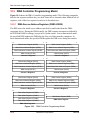
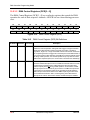
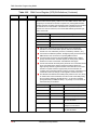
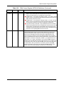
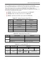
DMA Controller Programming Model
Table 10-5
DMA Control Register (DCR) Bit Definitions (Continued)
Bit Number Bit Name Reset Value
3–2
DDS
Description
DMA Destination Space
Specify the memory space referenced as a destination by the DMA.
NOTE: In Cache mode, a DMA-to-Program memory space has some limitations
(as described in the chapter on the Instruction Cache Controller and the chapter
on Operating Modes and Memory Spaces).
1–0
DSS
DDS1
DDS0
DMA Destination Memory Space
0
0
X Memory Space
0
1
Y Memory Space
1
0
P Memory Space
1
1
Reserved
DMA Source Space
Specify the memory space referenced as a source by the DMA.
NOTE: In Cache mode, a DMA-to-Program memory space has some limitations
(as described in the chapter on the Instruction Cache Controller and the chapter
on Operating Modes and Memory Spaces).
DSS1
DSS0
DMA Source Memory Space
0
0
X Memory Space
0
1
Y Memory Space
1
0
P Memory Space
1
1
Reserved
10.5.3.5.1 Non-3D Addressing Modes (D3D = 0)
If D3D = 0, the DAM bits are separated into two groups as described in Table 10-6:
■
DAM[5 – 3]: Defines the destination address generation mode
■
DAM[2 – 0]: Defines the source address generation mode
Note:
Motorola
The destination and source address modes can be chosen independently, but
they always use the same counter and, depending on the selected modes, they
can also use the same offset register.
DMA Controller
10-21