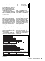
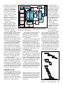
1
EMBEDDEDPC MONTHLY SECTION CIRCUIT CELLAR INK ® THE COMPUTER APPLICATIONS JOURNAL #101 DECEMBER 1998 EMBEDDED PROGRAMMING Achieving Better Design Communication with UML C and Assembly Language— When to Use What A Real-Time Multitasking Executive PICs and PCs Come Together the Embedded Way $3.95 U.S. $4.95 Canada TASK MANAGER The Word is Communication w hen I think of programming, it occurs to me that it’s just one of many types of communication. Whether you’re trying to get information from computer to computer or from person to computer, it’s still the same goal: the sharing of information that will (hopefully) prove useful to someone somewhere. Maybe one of the reasons that useful communication has become so relevant to me has to do with my recent trip out to the Embedded Systems Conference in San Jose. And this has more to do with getting useful information from person to person. On the one hand, Circuit Cellar had its own announcements to make. I had the privilege of speaking at a breakfast hosted by Motorola’s Semiconductor Products Sector. The point of the event was to introduce Motorola’s new family of 8-bit flash-based 68HC908GPxx microcontrollers, with the first product being the ’GP20. But my agenda was the launch of Design99, Circuit Cellar’s eleventh annual design contest. Prize-wise, it’s the biggest design contest we’ve ever offered, with five $5000 first prizes and twenty $1000 second prizes. Details concerning both the contest and the ’GP20 are posted at www.circuitcellar.com. But that presentation was also exciting for me because I had the opportunity to talk about the incredible year Circuit Cellar has had. In 1998, January marked the tenth anniversary, November was the 100th issue, and now this: a design contest sponsored by the world’s largest producer of MCUs. Hey, is this like Microsoft bundling some small company’s software? Then again, at the show, I also ran into some PR and marketing types who needed me to explain what you already know. Circuit Cellar is an engineering applications magazine for the engineer, the end user; not the marketing folks. Happily, even some marketeers found it an exciting—even novel—approach. One director of marketing that I met with called Circuit Cellar a “sleeper,” saying that he was tired of obnoxious, sales-oriented publications. He recognized that Circuit Cellar has value. Naturally, I agree. Those were the kinds of conversations that started the dialog going. Who we are. What we’re doing. What’s our goal. Who do we serve. The most important answer: we serve the engineer. What good is “advertorial” that isn’t useful to the engineer? And who better to know what is useful than engineers themselves, right? That’s why, best of all, it was so great to meet with the real designers, the ones who know about Circuit Cellar, who seek us out, who don’t send in the marketing reps, but who want to talk to us directly about their latest projects. And I know you want to hear about them: single-chip embedded Internet platforms, the 1451.2 standard, ASIC how-tos, motion control,… and there are so many more. Thanks to all of your input, I know 1999 is going to be even more spectacular! [email protected] 2 Issue 101 December 1998 Circuit Cellar INK® INK ® THE COMPUTER APPLICATIONS JOURNAL EDITORIAL DIRECTOR/PUBLISHER Steve Ciarcia MANAGING EDITOR Elizabeth Laurençot CIRCULATION MANAGER Rose Mansella TECHNICAL EDITORS Michael Palumbo Rob Walker CHIEF FINANCIAL OFFICER Jeannette Ciarcia ART DIRECTOR KC Zienka WEST COAST EDITOR Tom Cantrell ENGINEERING STAFF Jeff Bachiochi CONTRIBUTING EDITORS Ingo Cyliax Ken Davidson Fred Eady PRODUCTION STAFF Phil Champagne John Gorsky James Soussounis NEW PRODUCTS EDITOR Harv Weiner Ingo Cyliax ASSOCIATE PUBLISHER Sue Skolnick PROJECT EDITOR Janice Hughes EDITORIAL ADVISORY BOARD Norman Jackson David Prutchi Cover photograph Ron Meadows—Meadows Marketing PRINTED IN THE UNITED STATES ADVERTISING ADVERTISING SALES MANAGER Bobbi Yush Fax: (860) 871-0411 (860) 872-3064 E-mail: [email protected] ADVERTISING COORDINATOR Valerie Luster (860) 875-2199 Fax: (860) 871-0411 E-mail: [email protected] CONTACTING CIRCUIT CELLAR INK SUBSCRIPTIONS: INFORMATION: www.circuitcellar.com or [email protected] TO SUBSCRIBE: (800) 269-6301 or via our editorial offices: (860) 875-2199 GENERAL INFORMATION: TELEPHONE: (860) 875-2199 FAX: (860) 871-0411 INTERNET: [email protected], [email protected], or www.circuitcellar.com EDITORIAL OFFICES: Editor, Circuit Cellar INK, 4 Park St., Vernon, CT 06066 AUTHOR CONTACT: E-MAIL: Author addresses (when available) included at the end of each article. ARTICLE FILES: ftp.circuitcellar.com For information on authorized reprints of articles, contact Jeannette Ciarcia (860) 875-2199 or e-mail [email protected]. CIRCUIT CELLAR INK®, THE COMPUTER APPLICATIONS JOURNAL (ISSN 0896-8985) is published monthly by Circuit Cellar Incorporated, 4 Park Street, Suite 20, Vernon, CT 06066 (860) 875-2751. Periodical rates paid at Vernon, CT and additional offices. One-year (12 issues) subscription rate USA and possessions $21.95, Canada/Mexico $31.95, all other countries $49.95. Two-year (24 issues) subscription rate USA and possessions $39, Canada/Mexico $55, all other countries $85. All subscription orders payable in U.S. funds only via VISA, MasterCard, international postal money order, or check drawn on U.S. bank. Direct subscription orders and subscription-related questions to Circuit Cellar INK Subscriptions, P.O. Box 698, Holmes, PA 19043-9613 or call (800) 269-6301. Postmaster: Send address changes to Circuit Cellar INK, Circulation Dept., P.O. Box 698, Holmes, PA 19043-9613. Circuit Cellar INK® makes no warranties and assumes no responsibility or liability of any kind for errors in these programs or schematics or for the consequences of any such errors. Furthermore, because of possible variation in the quality and condition of materials and workmanship of reader-assembled projects, Circuit Cellar INK® disclaims any responsiblity for the safe and proper function of reader-assembled projects based upon or from plans, descriptions, or information published in Circuit Cellar INK®. Entire contents copyright © 1998 by Circuit Cellar Incorporated. All rights reserved. Circuit Cellar and Circuit Cellar INK are registered trademarks of Circuit Cellar Inc. Reproduction of this publication in whole or in part without written consent from Circuit Cellar Inc. is prohibited. 14 In-System Programming Rewriting the Book Craig Pataky and Bill Maggs 20 26 A Minimalist Multitasking Executive Richard Man and Christina Willrich 32 Some Assembly Required Assembling C Code for Your Embedded System Michael Smith 42 68 Smart Battery Systems Ed Thompson I MicroSeries Digital Processing in an Analog World Part 3: Dithering Your Conversion David Tweed 74 I From the Bench Learning to Fly with Atmel’s AVR Jeff Bachiochi 80 Object-Oriented Design of Real-Time Systems A Multidisciplinary Challenge Irv Badr I EMBEDDEDPC UE 48 Nouveau PC edited by Harv Weiner 59 APC 2 Reader I/O 6 New Product News edited by Harv Weiner 8 INK On-line 13 Advertiser’s Index/ January Preview 95 Priority Interrupt Steve Ciarcia Embedded Happenings 96 Silicon Update Hot Chips X Files Tom Cantrell INS I ISS DE 53 RPC Task Manager Elizabeth Laurençot The Word is Communication 101 Real-Time PC Embedded RT-Linux Part 2: Working with Flash Memory Ingo Cyliax Applied PCs emWare Top to Bottom Part 2: Launching the Application Fred Eady Circuit Cellar INK® Issue 101 December 1998 3 READER I/O Gerard Fonte’s recent article, “Breaking Nyquist”, (INK 99) evoked more than just a few casual responses from INK readers. Here’s a bit of I/O on the topic: What Gerard doesn’t seem to understand is that if you’re sampling a signal at 10 kHz and also at 9 kHz, you’re effectively sampling at 19 kHz, not 10 kHz. The theoretical Nyquist limit is 9.5 kHz and there’s no chance to detect arbitrary signals above this point. Using this method becomes unnecessarily complex when you can sample at 20 kHz in the first place! Since the premise is that 10 kHz is the highest rate, the output of two alternating 10-kHz ADCs would be fed into the DSP. That’s the same as a conventional system running at 20 kHz. Darrell Hambley [email protected] I hope you’ve been deluged with mail about “Breaking Nyquist.” I have 16 years of experience with the use and abuse of aliasing, and I see major theoretical and practical problems with this article. The starting premise is fine and might be paraphrased, if a signal frequency appears to shift significantly with a change in sample rate, at least one set of samples was aliased. Information theory dictates that a pint pot only contains a pint. Nyquist’s theorem stands because the effect of multiple sample frequencies is to form a higher sample rate. In Figure 5 (p. 32), the proposed (multiplexed-input and single ADC) version requires a very fast ADC. This is because some samples occur (1/fsa – 1/fsb) seconds apart or less (where fs is the sample rate, and a and b are sample paths). With only one ADC, some samples coincide, so one path must be dominant (introducing periodic noise if the paths are not very well matched). The width of the spectral lines produced by FFT or DFT depends mainly on the sample rate and sample size. Most, or all, of the center frequencies of two sets of spectral lines won’t line up if the sample rates differ. The method described adds the amplitudes at these unlike frequencies—a bit like adding apples to bananas. The analysis method is a version of the Vernier scale, which is over 100 years old. The Z-diagram is just an incarnation of f, 2fs–f, 2fs+f, 4fs–f, and on (i.e., 2nfs±f), known as frequency foldback, and is used daily in the rotating machinery industry on pumps, gas turbines, and such. I hope these aren’t considered novel. The parting shot hints at a swept or chirp style sampling method. For those brave enough to use it, the analysis math for nonuniformly spaced sampling has already been done elsewhere. A better solution, known as a time-slip or incremental-delay method, is older than some hills and makes few demands on the hardware. Paddy McKee [email protected] To address Darrell’s point first, in the section RealWorld Considerations, I discussed choosing a sample rate. “Let’s choose 9 kHz. The sum of the A/D rates is 19 kHz, which is close to the conventional example of 20 kHz” (p. 34). I included that example to show that relaxed input filtering can be used with a conventional rate. Secondly, in Figure 5 there are nonmultiplexed inputs—either two ADCs or two sample-holds. And, Figure 4 would require a very fast ADC if nonrepetitive signals were to be measured. But, in the Implementation section, I stated that “the method is suitable for systems with constant or repetitive signals” (p. 33). I’m aware of the 1/fsa – 1/fsb obstacle and why Figure 4 is limited. That’s why I included Figure 5. The 1/fsa – 1/fsb consideration wasn’t mentioned because every detail can’t be covered in one article. Nowhere in my article is a method described for adding the spectra. In the Implementation section, I state, “Since the sample rate affects the characteristics of the FFT, the spectrum comparison routine won’t be completely trivial” (p. 33). Also, I pointed out why direct addition or comparison of spectral lines won’t work. As for the Z-diagram, its purpose is to illustrate frequency foldback. The diagram was novel to me because I had been unfamiliar with it. Certainly, the chirp-to-Z transform isn’t for the faint of heart, but I’m not trying to reinvent FFT and all subsequent work. In the More Samples section (p. 34), I admitted that the math corrections aren’t trivial and that work is progressing slowly. Of course, when it comes to ideas, it’s easy to find reasons why something won’t work. It’s more rewarding (though often more difficult) to find a way to make it work—that’s the essence of being an entrepreneur. Gerard Fonte STATEMENT REQUIRED BY THE ACT OF AUGUST 12, 1970, TITLE 39, UNITED STATES CODE SHOWING THE OWNERSHIP, MANAGEMENT, AND CIRCULATION OF CIRCUIT CELLAR INK, THE COMPUTER APPLICATIONS JOURNAL, published monthly at 4 Park Street, Vernon, CT 06066. Annual subscription price is $21.95. The names and addresses of the Publisher, Editorial Director, and Editor-in-Chief are: Publisher, Steven Ciarcia, 4 Park Street, Vernon, CT 06066; Editorial Director, Steven Ciarcia, 4 Park Street, Vernon, CT 06066; Editor-in-Chief, Steven Ciarcia, 4 Park Street, Vernon, CT 06066. The owner is: Circuit Cellar, Inc., Vernon, CT 06066. The names and addresses of stockholders holding one percent or more of the total amount of stock are: Steven Ciarcia, 4 Park Street, Vernon, CT 06066. The average number of copies of each issue during the preceding twelve months are: A) Total number of copies printed (net press run) 29,783; B) Paid Circulation (1) Sales through dealers and carriers, street vendors, and counter sales : 4,270, (2) Mail subscriptions: 20,922; C) Total paid circulation: 25,192; D) Free distribution by mail (samples, complimentary, and other free): 1,404; E) Free distribution outside the mail (carrier, or other means): 160; F) Total free distribution: 1,564; G) Total Distribution: 26,756; H) Copies not distributed: (1) Office use leftover, unaccounted, spoiled after printing: 321; (2) Returns from News Agents: 2,706; I) Total: 29,783. Percent paid and/or requested circulation: 94.2%. Actual number of copies of the single issue published nearest to filing date are: (November 1998, Issue #100) A) Total number of copies printed (net press run) 30,200; B) Paid Circulation (1) Sales through dealers and carriers, street vendors, and counter sales: 4,647, (2) Mail subscriptions: 21,767; C) Total paid circulation: 26,414; D) Free distribution by mail (samples, complimentary, and other free): 1,050; E) Free distribution outside the mail (carrier, or other means): 240; F) Total free distribution: 1,290; G) Total Distribution: 27,704; H) Copies not distributed: (1) Office use leftover, unaccounted, spoiled after printing: 562; (2) Returns from News Agents: 1,934; I) Total: 30,200. Percent paid and/or requested circulation: 95.3%. I certify that the statements made by me above are correct and complete. Susan Skolnick, Associate Publisher. 6 Issue 101 December 1998 Circuit Cellar INK® NEW PRODUCT NEWS DSP-BASED MOTOR CONTROLLER The ADMC331 is a DSP-based motor controller featuring power-factor correction control capabilities. It provides a 26-MIPS, 16-bit fixed-point DSP core integrated with a 10-bit ADC and peripherals for controlling AC induction, synchronous permanent magnet, brushless DC, and switchedreluctance motors. The powerfactor control peripherals eliminate the need for discrete or IC-based active power factor control of the power supply. The ADMC331 includes a user-programmable three-phase 16-bit, center-based PWM generation unit to produce highaccuracy PWM signals with minimal software overhead. Its seven-channel, 10-bit ADC is synchronized to the PWM switching frequency and can provide 12 bits of resolution at lower switching frequencies of 6 kHz. Power-factor correction is enabled by a programmable auxiliary PWM circuit, enabling control of frequency, duty cycle, and phase shift on two dedicated Edited by Harv Weiner high-frequency PWM outputs. These signals are useful in front-end switching power-factor correction stages. Additional on-chip peripherals include a 16-bit watchdog timer and 24-bit DIO ports. Two flexible double-buffered bidirectional synchronous serial ports enable a variety of communication protocols. The program memory includes 2K × 24-bit RAM and 2K × 24-bit ROM. Data memory includes 1K × 16-bit RAM. Both can be boot loaded through the serial port from a serial ROM, EEPROM, or UART or synchronous connection. As well, the ROM motor-control functions support an interactive mode. The ADMC331 is available in an 80-pin TQFP package and costs under $5 in large quantities. Analog Devices, Inc. (781) 937-1428 Fax: (781) 821-4273 www.analog.com/motorcontrol OPEN SOURCE OPERATING SYSTEM Cygnus Solutions has announced eCos, a full-featured run-time solution that is under open source licensing terms. This highly configurable, application-specific operating system is targeted at embedded systems devel- opment. The complete eCos environment includes all kernel components, HAL layers, ulTRON configuration, C runtime, math libraries, and drivers. The source-level configuration (more than 170 configuration points) means that this OS can exactly match the needs of the application. eCos provides an open source infrastructure that enables embeddedsystem developers to focus on differentiating their products, rather than the development, maintenance, or configuration of a real-time kernel. The addition of eCos to Cygnus’s GNUPro environment provides developers with basic components like compilers, debuggers, and real-time kernels. Cygnus’s eCos is a royalty-free OS. Pricing for tools and support offered with the eCos Partner Program starts at $3500 per engineering seat. Cygnus Solutions (800) CYGNUS1 • (408) 542-9600 Fax: (408) 542-9699 www.cygnus.com 8 Issue 101 December 1998 Circuit Cellar INK® NEW PRODUCT NEWS POWER-MANAGEMENT SUPERVISORS The IMP705, IMP706, IMP707, IMP708, and IMP813L low-power microprocessor supervisor ICs integrate power-supply monitoring and microprocessor/microcontroller watchdog functions into compact eight-pin MicroSO packages. Besides ensuring that the system microprocessor or microcontroller is adequately powered or has restarted properly after a power failure or brownout, they integrate functions that monitor processor operation and issue system-initialization signals when system failures or lockups are detected. Each device generates a reset signal during powerup, powerdown, and brownout conditions. A separate power-fail-detection circuit with a 1.25-V threshold checks battery levels or non-5-V supplies. All devices have a manual reset input. The ’705, ’706, and ’813L feature a watchdog timer output that goes low if the watchdog input is not triggered within 1.6 s. The ’813L has the same pinout and functions as the ’705 but has an active-high reset output. The ’707 and ’708 have active-high and active-low reset outputs instead of a watchdog function. 10 Issue 101 December 1998 Circuit Cellar INK® The ’705, ’706, and ’813L monitor the power supply and battery in microprocessor and digital systems. A reset signal is generated whenever the supply voltage drops below 4.65 V for the ’705, ’707, and ’813L and below 4.40 V for the ’706 and ’708. In 1000 quantities, pricing for the ’705, ’706, and ’813L is $0.75, and the ’707 and ’708 cost $0.72. IMP, Inc. (408) 432-9100 • Fax: (408) 434-0335 • www.impweb.com NEW PRODUCT NEWS 68338 COMPUTER MODULE The Persistor CF1 is a modular microcomputer system using CompactFlash (CF) technology to extend the range of remote and portable data acquisition. The 1.4″ × 2.5″ × 0.5″ unit gives instant access to all microcomputer resources, including 68020 processing power, a DOS-like OS, and up to 48 MB of secure, transportable CF storage. The CF1 features an integral PicoDOS OS running on a 16-MHz Motorola 68CK338, coupled with 1-MB program flash and 256-KB battery-backed SRAM. It has an onboard 3.3-V linear regulator, power-management circuitry that reduces current drain to below 5 µA, realtime clock, dual RS-232 driver, QSPI interface, 15 counter/ timers, and full 16-bit bus expansion. The developer’s CD offers projects with commented source code and HTML descriptions. The PicoLog RecipeCard (a 3″ × 5″ circuit board) turns the Persistor into an eight-channel, 12-bit, analog recorder that samples at variable rates up to 1 kHz and stores to CF files. PicoDOS uses DOS prompts and commands, runs batch and executable files, and lets CF1 programs read and write files on CF cards using the standard DOS/ Windows media format. CF1 programs are written in ANSI C and C++ using Metrowerks’ CodeWarrior Professional compiler running under Win95/98/NT or Mac OS. PicoDOS provides a 250+ firmware function library and API featuring driver support for all of the standard C/C++ library functions and C-language interfaces to the 68338’s many integrated peripherals. Persistor CF1 costs $395 (or $295 in OEM quantities). Persistor Instruments, Inc. (508) 563-7192 • Fax: (508) 563-7191 www.persistor.com 16-BIT DATALOGGING STORAGE SCOPE The ADC-216 virtual digital scope combines the functions of a 300-kilosamples/s, dual-channel digital oscilloscope and 150-kHz spectrum analyzer in a PCbased virtual instrument that connects to a computer’s parallel port. Its 16-bit resolution is suited to precision applications like calibration, audio development and test, and vibration analysis. The supplied PicoScope software can operate simultaneously as an oscilloscope, spectrum analyzer, multimeter, and datalogger. Features include onscreen help, pull-down menus, and the ability to overlay a live trace with a stored reference trace. Powerful triggering modes help to capture intermittent or unusual events. Save On Trigger saves every trigger event to disk, complete with date and time stamp. It’s easy to transfer the data to other applications. A user can automate data collection and analysis using the software drivers supplied. The auto-ranging multimeter features simultaneous display of multiple parameters such as true RMS or DC voltage, decibel gain, and frequency measurements. Software drivers are supplied for users who want to program Windows NT, LabVIEW, Excel, and Visual Basic applications. The direct computer hookup provides the ability to annotate, save, and print traces on ordinary or networked printers in black and white or color. ADC-216 comes ready-to-use with software, cables, and power supply at $799. A 12-bit version, the ADC212, is available at $499. Saelig Company (716) 425-3753 • Fax: (716) 425-3835 • www.saelig.com Circuit Cellar INK® Issue 101 December 1998 11 NEW PRODUCT NEWS ECONOMICAL LOAD AND FORCE SYSTEM TeKscan has announced a simple load-measurement system that uses single-element sensors. The ELF system uses a serial interface, Windows software, and innovative electronics to provide an economical solution to measurement problems. Applications include variable force control for joysticks, occupant detection, weight measurement and distribution, and fill rates and pressures. The ELF system is durable, accurate, and simple to use. The system allows for nonintrusive measurement, and the sensors are small enough to allow for precise placement. The thin sensors (0.005″, 0.127 mm) can be attached to many surfaces. They can also be combined with plastic or metal films for increased stiffness or for added protection from their environment. The software is simple to use and easy to interpret. It is possible for users to read static or dynamic forces in real time or record a “movie” and view the information in a choice of graphical displays. The information can then be viewed as a strip chart, bar graph, analog meter, or digital display. Logic Analyzers 12 Issue 101 December 1998 Circuit Cellar INK® The FlexiForce ELF sells for $299, and custom sensor designs are available. FlexiForce (617) 269-8373 • Fax: (617) 269-8389 www.tekscan.com December Design Forum password: Code INK ON-LINE Your magazine enjoyment doesn’t have to stop on the printed page. Visit Circuit Cellar INK’s Design Forum each month for more great online technical columns and applications. Here are just some of the great new on-line articles you’ll see in December: Columns Silicon Update Online: The End of Architecture?— Tom Cantrell Lessons from the Trenches: Getting a Head Start on Software Development—Setting It Up for the Target—George Martin Forum Feature Articles When Can You Sell an Idea Without Losing Your Patent Rights?—Breffni Baggot A Serial Word Generator—Raymond Dewey PIC Abstractions Design Abstracts from our Design98 Contest A PIC12C508 Multichannel Remote Control Transmitter—Robert Larson Data-Mate—Tony Webby Eclipsing Sun Visor—Robert E. Johnson Missing the Circuit Cellar BBS? Then don’t forget to join the Circuit Cellar INK newsgroups! The cci newsserver is the engineer’s place to be on-line for questions and advice on embedded control, announcements about the magazine, or to let us know your thoughts about INK. Just visit our home page for directions to become part of the newsgroup experience. www.circuitcellar.com Circuit Cellar INK® Issue 101 December 1998 13 FEATURES 14 In-System Programming 20 A Minimalist Multitasking Executive 26 Object-Oriented Design of Real-Time Systems 32 Some Assembly Required 42 FEATURE ARTICLE Craig Pataky & Bill Maggs In-System Programming Rewriting the Book Smart Battery Systems IS people got it made, don’t they? Instant reprogrammability means you don’t have to sweat the details. Craig and Bill show how system engineers can have that luxury, too, with an in-system programmable target platform. a ny experienced software engineer can relate to the knotsin-the-stomach feeling when a new EPROM is released to production. Sure, it’s time to celebrate, but it’s also the time to review the “wish I woulda’s” and “things I forgot.” All your mistakes are about to be duplicated in every one of a thousand units coming off the line, and there’s nothing you can do about it. Once that PROM or OTP is soldered to the board, your fate is sealed. It’s even worse if the final product is forever locked in a coffin of potting compound. A latent design flaw in a datalogger may not show up for months. No wonder firmware SEs are so jumpy. Of course, a lot of the pressure can be relieved if the target platform is insystem programmable, like a PC. After all, the IS department doesn’t sweat with each tweak to the e-mail system. DIVERGENT DESIGNS Truth is, the IS folks have long enjoyed the luxury of instant reprogrammability because, as far as a desktop PC is concerned, code memory is the same as data memory and can be 14 Issue 101 December 1998 Circuit Cellar INK® arbitrarily read, written, or executed from. This design is called the Von Neumann or Princeton architecture. On the other hand, embedded controllers have separate areas for code and data memory. This design is referred to as the Harvard architecture. The main reason microcontrollers have clung to the Harvard architecture is because by keeping data and code memory separate, it’s impossible for the machine to inadvertently corrupt its own code and go insane. Unfortunately, the strict Harvard architecture also prevents the microcontroller from performing intentional code rewrites. That’s why so many technicians have spent so many hours swapping EPROMs. Von Neumann designs are flexible but inherently unstable. Harvard designs are rock-solid but immutable. Clearly, with design cycles crunching ever downward, something has to give. ADAPTATIONS Almost every engineer has run into the Von Neumann/Harvard problem. Generally, the solution falls into one of two categories—simply executing tokens stored in some form of nonvolatile memory (NVM), or swapping banks of code and data spaces so one bank can be written while the controller executes from the other. The BASIC Stamp from Parallax is an excellent example of token execution. Ours is built from a PIC16C56 and 93C56 NVM. When I write a program in PicBasic and upload it to the Stamp, I’m really sending tokens to the PIC to represent commands like FOR..NEXT and GOTO. The PIC stores these tokens in the NVM. Later, the PIC executes these tokens by fetching them from the NVM, figuring out what each token means and carrying out the instruction. These PicBasic tokens are not opcodes native to the PIC—the PIC is executing native code out of its ROM to interpret PicBasic tokens on-the-fly. It’s like getting a secret message and using your decoder ring to read it. The overhead in token processing is immense. An instruction such as A=B may take hundreds of times longer than it would if the device were executing native opcodes. Still, this method is inexpensive and, until recently, was the only real solution. But, its Achilles heel is obvious— what if the bug is in the interpreter? Fortunately, Parallax has excellent quality control and my Stamp has shown no signs of misbehavior. As we mentioned, swapping banks of external code and data space is an alternative to interpreting tokens. This method was not truly viable until the advent of the 5-V flash memory. Its implementation is conceptually simple but somewhat more difficult to realize. The steps to completely reprogramming a system using the bankswap method go in this order. The microprocessor wakes up and starts executing out of flash bank A (code memory). When it’s time to reprogram, the controller writes new code into flash bank B (data memory). The microcontroller then executes an instruction common to both old and new code, which swaps banks A and B. Now, bank A is data memory and bank B is code. The controller then copies bank B to bank A. When the rewrite is complete, the controller may starve the watchdog or perform some self-reset, thereby waking up again to execute code out of the newly rewritten bank A. Although cumbersome, the advantage of this method is apparent. Instead of decoding tokens, your micro is free to execute native opcodes. Rather than using a special compiler to generate the tokens, you can use an off-the-shelf compiler or assembler for the target. Unfortunately, this approach may cost your design an extra $15 for the flash memory and glue logic involved. Though both solutions work, neither is optimal. Executing tokens is too slow for many applications, and increasing the component cost in the name of flexibility doesn’t appeal to the end user. After all, shouldn’t we get it right the first time? Gulp. LATEST REFINEMENT Responding to the need for low-cost in-system reprogrammability, several manufacturers are equipping devices with built-in rewritable code memory. The key word here is rewritable. Pin Direction Signal 1 out control bit 0 2 out data bit 0 3 out data bit 1 4 out data bit 2 5 out data bit 3 6 out data bit 4 7 out data bit 5 8 out data bit 6 9 out data bit 7 10 in data bit 6 11 in data bit 7 (inverted) 12 in data bit 5 13 in data bit 4 14 out control bit 1(inverted) 15 in data bit 3 16 out control bit 2 17 out control bit 3 (inverted) 18–25 gnd — Note that direction is relative to the PC. Table 1—The 25-pin parallel port is standard on all IBM-compatible PCs and offers 17 pins capable of doing useful work (12 outputs and 5 inputs). In-system programming (ISP) has been around for many years but only in OTP devices. But, Atmel and Dallas are already shipping production quantities, and similar products are soon to follow from Microchip and Philips. This means the days of socketed EPROMs, masked parts, and OTPs are gone. Now, you can solder a controller directly to the PCB and program it just before shipment. More importantly, you can reprogram that same controller. ATMEL ISP Now, we’d like to narrow the focus to the Atmel 89Sxx series of 8051compatible ISP microcontrollers with integrated flash and E2. We’ve been designing with this family for the last year, and because the device is a mere $10 in quantity, we’re building it into all of our new products. The Atmel ISP family comprises the 89S8252 and the 89S53. The 89S8252 has 8-KB ISP code memory and 2-KB ISP E2 data memory, whereas the 89S53 has 12-KB ISP code memory but no ISP E2 data memory. According to Atmel, arm yourself with the 89S series, and software modifications are as simple as the wave of a wand. Truly, we live in times of reprogrammable bliss. WELL, NOT QUITE Of course, any significant innovation is useless if it you can’t take advantage Circuit Cellar INK® Issue 101 December 1998 15 appropriate ISP pins. The of it. This is the one area where Atmel came up short. parallel port was the obvious Although the ISP nature choice. of the 89Sxx series promises As mentioned in “Beyond to revolutionize the design The Box With Windows 95,” cycle, Atmel didn’t provide (INK 74) even the most basic any utilities to get our binaparallel port has 12 readily ries into the chip. accessible TTL outputs and Their documentation was 5 inputs. The useful signals cryptic at best. The dataare shown in Table 1. sheets are concise about Figure 1 shows the what pins and hex values adapter needed to interface should be used to program a the parallel port of the PC controller, but alas, should to the Atmel ISP port. We Figure 1—We couldn’t establish reliable communications without a buffer IC, underthe data be clocked in MSB tapped 5 V from our target standably due to the TTL to CMOS connection. The 74HC125 was convenient but or LSB? On the rising edge micro to power our buffer. any noninverting buffer will do. or the falling edge? On which Without taking power from edge should the reply data be read? our target, we’d have to use an exterprogrammers aren‘t up to the task of All we wanted was a simple internal power supply or tap the 5-V line creating the hardware, and most hardface to attach to the parallel ports of from the PC’s keyboard port. Just bring ware designers can’t write the utility. our PCs and then, at the DOS prompt, an extra line out from your target, and But despite the obstacles, we created to be able to type something like ISP an interface to attach to the PC’s you’re ready. MYPROG.BIN. Was it too much to ask? parallel port and some software to download files to the 89S on the PCB. SOFTWARE DIGGING IN We created the ISP utility, ISP.EXE, Clearly, the burden of programming HARDWARE as a straightforward program for DOS, the controller is left up to the design Our first step was to try and directly and it’s exactly what Atmel should engineer. Unfortunately, most PC connect the parallel port pins to the have provided all along. We chose the Circuit Cellar INK® Issue 101 December 1998 17 /c:filename /d:filename /p:[1|2|3] /e /r /s:[0-9] /h or /? Program code memory with the indicated file Program nonvolatile data memory with the indicated file Select which parallel port to use Erase the entire chip before programming Invert the reset line Set programming speed, 0 being fastest Display all the command line options DOS platform because ’486, ’386, and even ’286 computers always make it onto the production floor when the rest of the company upgrades. The ISP utility gets binary files off your hard drive and into the 89S. The utility supports a few command line options to make it generic. For example, if your programming interface is attached to LPT2 and FOOBAR.BIN is your binary file, typing isp.exe /p:2 /c:foobar.bin should begin the upload operation. Table 2 lists the ISP command line options. We included the set programming speed (/s:[0-9]) option because the rate at which an 89S can be programmed is directly affected by its crystal. Although an 89S running at 20 MHz might program fine at speed 0, the same chip at 1 MHz probably requires an ISP speed setting of 9. We’d also like to point out the invert reset line (/r) option. Part of the ISP operation is keeping the microcontroller in a reset state for the duration of the programming cycle. The default operation of the ISP utility holds the reset line high while programming, but the /r option was provided in case you’ve interfaced your microcontroller’s reset line through an inverting buffer of some kind. HEX2BIN Most of the 8051 compilers we’ve used generate only a hex file and not a binary file. Intel hex was originally created to make our generated files easier to view and transport. But, processor cores prefer the true binary opcodes and data to ASCII codes. If your compiler generates a binary file, use it. If it generates an Intel hex format file, we also provide a HEX2BIN utility to perform the conversion. Type HEX2BIN myfile.hex and the appropriate translation is made. Table 2—Some ISP command line options are provided to make the utility generic, while others are designed to accommodate the programming variables that may exist. HITTING THE MARK We’ve covered broad design considerations as well as specific solutions. Even if Atmel is not your style, several manufacturers are likely to be sampling similar solutions by year’s end. As you know, the winners in this business are light on their feet, react quickly, and cater to customer demands. ISP makes those three goals just a little easier to reach. I Craig Pataky is a systems engineer with over nine years of experience ranging from simple embedded programming to OS design. You may reach him at [email protected]. Bill Maggs is an electrical engineer with over eight years of embedded design experience. His designs range from low-power handheld devices to fixed-station monitoring equipment. You may reach him at www.logic fire.com. SOFTWARE Source code for this article is available via the Circuit Cellar web site. SOURCES 89Sxx microcontrollers Atmel Corp. (408) 441-0311 Fax: (408) 436-4200 www.atmel.com PIC16C56 Microchip Technology, Inc. (602) 786-7200 Fax: (602) 899-9210 www.microchip.com BASIC Stamp Parallax, Inc. (888) 512-1024 (916) 624-8333 Fax: (916) 624-8003 www.parallaxinc.com Circuit Cellar INK® Issue 101 December 1998 19 A Minimalist Multitasking Executive A multitasking executive might seem like a nice enhancement, but the costs are prohibitive, right? Well, maybe they don’t have to be. With µexec, even simple embedded programs can be written as multiple tasks. 20 Issue 101 December 1998 FEATURE ARTICLE Richard Man & Christina Willrich a typical embedded program reads data from input devices (ADC, keypad, serial port, etc.) and, after some processing, generates some output (LCD, pulses sent to drive motors, etc.). One simple and crude method of going through this process is to have a control loop as the main function, looping through all the things needing to be done. Listing 1 shows you an example. The problem is that often you don’t want to perform all the steps every time the code goes through the loop. Also, each subroutine must temporarily return to the control loop after some period of time and be able to resume from where it leaves off the next time it’s called. While this technique works for some programs, it’s usually more error prone and harder to use than using a multitasking executive. Listing 2 shows a program with a multitasking executive. Listing 2 looks similar to Listing 1, but the program is partitioned into independent tasks. The tasks don’t need to worry about returning control to a high-level function, and each task may run for a different amount of time before control transfers to another Circuit Cellar INK® task. In some executives, a task may even stop running altogether and wait on some resource to become available before it is run again. Since there’s only one CPU, in reality only one task is run at a time. What a multitasking executive does is to periodically take control of the CPU and allow other tasks to run. So, how does a multitasking system work? In a cooperative multitasking system, each task voluntarily yields control to the system. In the world of PCs, the Mac OS (until OS X) is an example of a cooperative multitasking system and so is Windows 3.1 and below (except, strangely, for the DOS boxes under Windows 3.1). In a preemptive multitasking system (e.g., Windows NT), the system interrupts a running task if other tasks must be run. A preemptive system is more powerful than a cooperative one because it’s easier to program and it enables tasks to run more fairly. Under a preemptive system, priorities can be assigned to tasks so the scheduler will run higher priority tasks first. A high-priority task that is waiting for a resource may interrupt a lower priority task if the resource becomes available. The multitasking executive we describe here is the preemptive type. Despite the benefits of a multitasking executive, it’s often not cost effective for most simple programs—or for people on a budget—to purchase a full-blown multitasking executive. Here, we show you a small multitasking executive, aptly named µexec (pronounced myoo-exec), written in ANSI C and some assembly routines. The supplied code is written for and tested on a Motorola ’HC11, but it should be easily ported to other microcontrollers of comparable power. The code is quite small, in fact, compiling to only 700 bytes using the ImageCraft ICC11 ’HC11 C compiler. µexec is a preemptive multitasking system, but to keep the code small, its tasks all have the same priority level. So, you can enjoy the benefits of a multitasking executive without paying a lot in cost or resource consumption. This article first gives a high-level description of µexec, including some Listing 1—This sample embedded program uses a control loop. Each time through the loop, several tasks are done in sequence. Control loop: check sensor 1 check sensor 2 compute pi to 347 digits contemplate and meditate activate death ray 1 drive motor goto control loop of the design choices. Next, we describe the data structures, followed by API functions and assembly routines. Most porting efforts are only needed in modifying the assembly routines, so skip to that section if you’re interested in porting µexec to your favorite microcontrollers or compilers. The last section gives a summary and ideas for enhancements. If you just want to use µexec, see the API descriptions for the interface functions. Under µexec, a task runs for a period of time until a timer interrupt interrupts it, and the µexec control system chooses another task to run. This process repeats indefinitely—at least until the system crashes, or interrupts are (accidentally) disabled, or the embedded system runs out of battery juice. TASK FUNCTION A µexec task is a C function that does not take an argument or return a result. Any such function can be made into a task via UEXC_CreateTask. Tasks can be created and killed dynamically, even within other tasks. Normally, a task function should not terminate (i.e., it should execute an infinite loop). If it does, µexec deletes it from the internal data structures. Typically, you create some tasks in your main routine and then start the scheduler running. After that, the processor executes your tasks and never returns to the main routine. Each task needs its own stack, which is supplied to the system when a task is created. Unfortunately, stack overrun (i.e., when a task uses stack space that is beyond the range of the supplied stack) can be a deadly problem. µexec checks the stack pointer of a task to ensure that it’s within bounds, but this check may not be of much value since a stack overrun may have already damaged important data, including µexec’s internal data structures. So, it’s best to be conservative and allocate a large stack for a task. In fact, if your system crashes mysteriously, try allocating larger stacks for your tasks. Stack overrun is a general problem in embedded programs. Multiple tasks exacerbate the problem because each task uses its own stack. If there is only one control loop, then all the functions execute with one stack and it is easier to be conservative with just that stack. Unfortunately, you have to pay the price for using a multitasking executive. SCHEDULING AND TIMESLICE The scheduler chooses which task to run. The period of time a task is allowed to run is called its timeslice. Under µexec, tasks are run to completion of their timeslices unless they are explicitly yielding control to the Listing 2—This program is the same as in Listing 1, but it is partitioned into separate tasks. The control loop is part of the multitasking executive. Task Task Task Task Task Task 1: 2: 3: 4: 5: 6: check sensor 1 check sensor 2 compute pi to 347 digits contemplate and meditate activate death ray 1 drive motor system or hogging the processor for another timeslice. Although µexec doesn’t assign priorities, tasks can have different timeslice lengths, so you can cause a compute-intensive task to run longer if necessary. The main purpose of the µexec control system, then, is to interrupt the processor at the end of a task’s timeslice and invoke the scheduler to choose another task to run. µexec uses a timer to interrupt the CPU at regular intervals. Almost all microcontrollers have timer interrupt functions that can be used for this purpose. For example, on the ’HC11, there are five timer-registers, each one of which can be set up to generate an interrupt when the timerregister’s value matches the value of the free-running timer counter. The time period when such an interrupt occurs is called a tick, and its timeslice is some multiple of ticks. A tick’s value should be chosen such that the processor is not interrupted too frequently, but it shouldn’t be so long that other tasks do not get to execute in a timely manner. For the ’HC11, we chose a value of 2000 cycles per tick, or about 25 µs for a ’HC11 running with an 8-MHz clock. The default timeslice is five ticks, or 125 µs. You may want different values for your system. INTERRUPT DRIVER Sometimes your program may need to perform some function at a regular interval, and task scheduling may be too slow and unpredictable. µexec gives a hook to the timer-interrupt handler— if the global variable UEXC_InterruptDiver is nonnull, then it’s assumed to contain the address of a function. The system timer-interrupt handler then calls this function before it performs other work. To use this feature, assign the address of your function to be called to this variable. TASK CONTEXT An important consideration is how to maintain the task’s context so that µexec can return control to a previously stopped task. Because µexec normally regains control through a timer interrupt, and that interrupt already saves the CPU states (e.g., the register values) Circuit Cellar INK® Issue 101 December 1998 21 on the stack, it is sufficient to only save the stack pointer of an interrupted task at the time the handler was entered. To resume a task, µexec reloads the stack pointer and uses the ReturnFromInterrupt instruction to restore control to the stopped task. From a task’s point of view, a timer interrupt hits, and some time later, the interrupt handler returns and execution continues. The fact that other tasks get a chance to execute while the task is stopped is invisible to the task. There is one additional place where the task context must be saved—when a task voluntarily gives up control using the UEXC_Defer function. In this case, UEXC_Defer constructs an interrupt-stack frame so that no special case handling is needed to resume the task. This scheme doesn’t work with processors using a separate interrupt stack from the user stack. Also, if a multitasking executive provides resource-waiting functions (semaphores, mailboxes, etc.), there are other places where task context must be saved. In these scenarios, it’s simpler to save the entire CPU context in the task data structure and not rely on the interrupt stack. Since µexec does not provide resource-waiting functions, and since most small microcontrollers don’t use a separate interrupt stack, using the interrupt-stack frame to save the task’s context is fast and effective. CODE COMMUNICATION Most of the µexec routines are written in C. A small number are in assembly, mostly to manipulate interrupt-stack frames. The format of passing arguments between routines is compiler-dependent, so we opted to use global variables to pass information between the assembly and C routines (of course, C routines calling other C routines use the standard C calling format). Only two global variables are needed. There are some minor differences in how each compiler handles global names. For example, some compilers prepend an underscore before a global name if it’s to be used by an assembly module, but these differences are easy to handle. 22 Issue 101 December 1998 Listing 3—The key data structure of a multitasking executive is its task control block. µexec’s task control block is described here as a C structure. enum {TCREATED, T_READY}; typedef struct TaskControlBlock { struct TaskControlBlock *next; unsigned char tid; /* task id */ unsigned char state; /* task state, do not use enum since compiler may allocate more space */ unsigned char ticks; /* how many ticks does task execute */ unsigned char current_ticks; /* number of ticks remaining */ void (*func)(void); /* function to call for that task */ unsigned char *stack_start; /* stack low value */ unsigned char *stack_end; /* stack high value */ unsigned char *sp; /* current value of stack pointer */ } TaskControlBlock; INTERRUPTS Interrupts must be carefully enabled and disabled inside µexec. If this is done improperly, unpredictable results occur. For example, if interrupts are left enabled while global data structures are being manipulated, a data structure may be in an inconsistent state and further accesses in an interrupt handler will crash the system. Of course, if interrupts are inadvertently disabled when resuming a task, the timer interrupt is also disabled and multitasking will stop. A simple enhancement is to use the watchdog timer presented in most microcontrollers to detect these kinds of system-crash errors. However, you need to have a mechanism for the system to either restart itself or report the errors. TASK CONTROL BLOCK The data structure TaskControlBlock (see Listing 3) describes a task. µexec keeps all tasks in a circular linked list and a global variable keeps track of the current task. To choose the next task to run, µexec follows the next pointer field of the current task and sets the currenttask variable accordingly. To ensure that there is always at least one task to run, the system creates a null task. It calls UEXC_Defer in an infinite loop, enabling other tasks to run. If no other task is there, the system runs this null task indefinitely. A task is identified by its task ID, which is kept in the tid field. ticks Circuit Cellar INK® is the number of ticks that the task should execute before scheduling occurs (i.e., its timeslice value). current_ ticks is the number of ticks left in the execution of this task. func is the pointer to the C function for the task. The stack start and end values are for debugging purposes, such as detecting stack overrun. sp is the current value of the stack pointer. It must be within the range of the start and end stack values. GLOBAL VARIABLES As most programmers have learned, global variables are generally not part of good code design. But, there are situations where their use is warranted. For example, under µexec, we use two global variables to pass information between C and assembly routines. The alternative is to use normal argument passing between the routines, but that would be compiler and microcontroller dependent, making it difficult to port µexec using other compilers or to other microcontrollers: void (*uexc_current_func)(void); unsigned char *uexc_current_sp; uexc_current_func is the pointer to the function for the current task and is needed only to start a new task. uexc_current_sp is the current stack pointer or the address of the sp field of the current task. The latter is used by UEXC_Defer to tell the assembly routine where to store the stack pointer after the interrupt frame is created. µexec uses a few other global variables and macros, such as static TaskControlBlock *current_ task;. This global variable points to the task-control block of the current task. All the tasks are linked in a circular list, so the next task to execute is given by current_task->next. void (*UEXC_InterruptDriver) (void); contains the address of a function to call whenever the timer interrupt triggers. If you have more than one function to call, you can chain them together. The NUM_TASKS macro is the maximum number of task-control blocks that can be allocated. You should change this to match the number of tasks you have in your system. The macro UEXC_MIN_STACK_SIZE defines the minimum stack size for a task. If your task function invokes other functions or uses local variables, you should allocate a bigger stack. MEMORY MANAGEMENT µexec needs to allocate memory to hold the task-control blocks and the tasks’ stacks. This allocation can be done by using the C-library function memory-management routines malloc and free or by using statically allocated global arrays. Since µexec is meant to be used in a small system, the overhead of and possible fragmentation of the memory space by using malloc and free are of concern. So, we use a simple array allocator instead. However, you can easily modify the system to use malloc and free. Task stacks are supplied as an argument to UEXC_CreateTask. You should define statically allocated arrays and supply them to UEXC_CreateTask: task is created. UEXC_Createtask fails if no more task-control blocks are available. The system initializes free_list_ ptr with the elements in free_list, so you can adjust the total number of task-control blocks by changing the value of NUM_TASKS. When a task is killed or when a task function returns, its task-control block is released back to the free_list_ptr pool. API In this section, we present the usercallable functions. The function prototypes and user-definable macros are in the file uexec.h. These functions are written in ANSI C, and they shouldn’t need modification to compile for other processors similar to the ’HC11 or under different compilers. As well, some of the internal C functions shouldn’t require any modification for porting purposes. The function int UEXC_CreateTask(void (*func)(void), unsigned char stack[], unsigned stack_size, int ticks); creates a task given the function func. Each task must have its own stack, given by the argument stack. This stack is the lowest address of the array (i.e., address of the zero’th static unsigned char task_stack[UEXC_MIN_STACK_SIZE]; All the task-control blocks are allocated from a global array: static TaskControlBlock free_list[NUM_TASKS], *free_list_ptr; A task-control block is allocated from the free_list_ptr every time a 24 Issue 101 December 1998 Circuit Cellar INK® element). Since stack usually grows from high addresses to lower addresses, the size of the stack is needed and is given by the argument stack_size. With the stack and stack size, the stack pointer can be checked against the bounds. If you port µexec to a processor that needs stack alignment, you need to align the stack properly. ticks is the number of ticks in this task’s timeslice. If it is zero, then the value given by the macro DEFAULT_ TICKS is used. UEXC_CreateTask obtains a taskcontrol block from the free list, initializes it with the supplied arguments, and links the task-control block into the circular task list. This function returns an integer task identifier. If the task function returns, then it acts as if the function UEXC_KillTask is called with the task’s ID. void UEXC_Defer(void); gives up the rest of the timeslice and lets other tasks run. This function calls an assembly routine to construct an interrupt-stack frame so that the task can be resumed by using ReturnFromInterrupt. This process is consistent when a task is interrupted by the timer and its timeslice runs out. void UEXC_KillTask(int tid); is a function that kills a task with the Listing 4—This trivial program tests µexec’s basic functionality. Two tasks are created, and each one prints out a different character on the output. #include "uexec.h" unsigned char task_zero_stack[UEXC_MIN_STACK_SIZE]; unsigned char task_one_stack[UEXC_MIN_STACK_SIZE]; void Zero(void) { while (1) putchar('0'); } void One(void) { while (1) putchar('1'); } void main(void) { UEXC_CreateTask(Zero, task_zero_stack, sizeof task_zero_stack), 0); UEXC_CreateTask(One, task_one_stack, sizeof (task_one_stack), 0); UEXC_StartScheduler(); } ID tid. It searches the task list to find the matching task and reclaims its storage after it unlinks it from the list. void UEXC_HogProcessor (void); hogs the processor and gives the current task another timeslice. If this function is called repeatedly before its timeslice is up, then no other tasks (except for the interrupt driver function) are run. It simply assigns the current_ ticks field of the task-control block with the ticks field. int UEXC_StartScheduler (void); is the code that starts the multitasking scheduler. It should be called in your main() routine after it creates some tasks. This function never returns to the caller, and control transfers to the created tasks unless no task was created prior to this call being made. It starts the timer interrupt and then calls the internal function Schedule to transfer control to a task. Finally, void (*UEXC_Interrupt Driver)(void); is not actually a function but a pointer to a function. If nonnull, it should contain the address of a function you wish to call at each timer interrupt. ASSEMBLY FUNCTIONS These functions need to be modified when porting µexec or if you choose to use a different timer counter instead of TOC4 (Timer Output Compare 4) under ’HC11. They don’t take any arguments or return any value, which should make them easy to port. In total, there are less than 50 assembly source lines, 10 of which deal with the timer registers and can actually be written in C. UEXC_SystemInterrupt is the timer interrupt handler. After storing the stack pointer to the global variable uexc_current_sp, it calls a function to see if the current task’s timeslice has run out. If it has, then a new task is scheduled and control transfers to the new task. If the timeslice has not run out, handler returns via ReturnFromInterrupt. You must arrange for this handler to be invoked for the appropriate timer interrupt. In most cases, this means putting the address of this function in the interrupt vector table. If you are using a debug monitor, typically the monitor provides a RAM-based pseudo-vector table. The function UEXC_SavregsAndResched is called by UEXC_Defer to create a fake interrupt stack. UEXC_StartNewTask is called to run a new task. The stack is set up so that if the task function ever returns, then an internal function, UEXC_KillSelf, is called. UEXC_KillSelf is equivalent to UEXC_KillTask (current_task->tid). The UEXC_Resume is a function that gets the stack pointer from uexc_ current_sp and does a ReturnFromInterrupt. The function UEXC_StartTimer can be written in C, but we put it in the set of assembler functions because it is microcontroller specific. It needs to set the timer registers to enable the timer interrupt at INTERRUPT_CYCLES later. TOC4 is used in the supplied code. Typically, a TOC function can be associated with an output pin, but in this case, the output pin function is disabled. The value given by INTERRUPT_ CYCLES is the system tick and must be adjusted for different system clock speeds. As supplied, it is defined to be 2000 (cycles). UEXC_RestartTimer can also be written in C. It simply reenables the timer interrupt at INTERRUPT_CYCLES later. GIVE IT A TRY The simple example shown in Listing 4 creates two tasks that print out 0s and 1s. In addition to traditional programming uses, µexec can be used to implement subsumption architecture, which is a powerful programming paradigm particularly suitable for programming autonomous robots. If you’re interested, we recommend checking out Mobile Robots, Inspiration to Implementation [1] for more detailed information on subsumption programming. ENHANCEMENTS In summary, µexec is a small, simple to use, simple to port, and yet useful multitasking executive. Its resource usage is modest, taking only about 700 bytes on an ’HC11. With this executive, even simple embedded programs can be written as multiple tasks, gaining you the benefit of having a preemptive executive. Naturally, there are plenty of possible enhancements, such as adding the watchdog timer function that comes with most microcontrollers to the system. As well, you might choose to modify the system so that error conditions can be reported via your system’s output mechanisms (serial port, LCD, or even just a blinking LED). Or, why not modify the system so that it prints out the maximum stack usage for each task? You can even add a name field to the task control block so that diagnostics can be printed with the task’s name. I Richard Man and Christina Willrich are the owners of ImageCraft, a company which specializes in low-cost professional ANSI C tools for microcontrollers, plus ’HC12 hardware and BDM debug Pods. You may contact them via www.imagecraft.com. SOFTWARE Complete source code for µexec is available via the Circuit Cellar and ImageCraft web sites. REFERENCE [1] J. L. Jones and A. M. Flynn, Mobile Robots, Inspiration to Implementation, A.K. Peters, Natick, MA, 1993. SOURCES 68HC11 microcontroller Motorola MCU Information Line (512) 328-2268 Fax: (512) 891-4465 www.mcu.motsps.com ICC11 ’HC11 C complier ImageCraft (650) 493-9326 (650) 493-9329 www.imagecraft.com Circuit Cellar INK® Issue 101 December 1998 25 FEATURE ARTICLE Irv Badr Object-Oriented Design of Real-Time Systems A Multidisciplinary Challenge During the design stage, the system, hardware, and software engineers all have their own issues and development tools. Irv presents a way to balance and coordinate the efforts so we can all speak a common language at last. 26 Issue 101 December 1998 d esigning realtime embedded systems involves a multidisciplinary team of engineers. System engineers get the process started, and because they are primarily concerned with the overall architecture, they often make tradeoffs that influence the hardware and software composition. Hardware engineers design circuitry that fulfills the system requirements as determined by the system engineers. And, because the majority of the system functionality lies in the software, the software engineers have the largest design and implementation task. Photo 1—There’s more than one way to incorporate hardware properties into the System Architecture diagram. In this case, the values refer to the RS-232 interface on the modem-controller board. Circuit Cellar INK® The challenge in coordinating these disciplines is compounded because all three have different concerns, use different tools, and work somewhat independently of one another. The system engineer, in an effort to refine system requirements and assess feasability, is concerned with state modeling of the control system or communications protocols. The hardware engineer tends to think in terms of processors and circuits within the domain of schematic capture, ASIC design, VHDL, circuit simulation, and board layout. The software engineer is thinking about functional decomposition or an object model. There’s no proven methodology to bridge these disciplines and implement a more collaborative system development. Most organizations rely on a document or drawing tool to capture system architecture. Although keeping that document current is challenging, making it relevant to the software engineer is more difficult. Few software engineers read schematic diagrams or other hardware documents when considering how to interface their software to the hardware. In this article, I consider the possibility of coordinating system, hardware, and software development by using object-oriented (OO) technology— specifically, the Unified Modeling Language (UML). The UML extensions are from Artisian Software Tools’ RealTime Studio, a tool designed to enable collaborative system development. UNIFIED MODELING LANGUAGE A result of the Object Management Group (OMG) and the efforts of many methodologists, UML has become the most widespread notational scheme for system modeling. It has made object-oriented modeling possible on a wide scale by standardizing a common language that spans multiple organizations and modeling tools. With UML, engineers can define a system-level design, regardless of many details. However, when used for real-time modeling, UML doesn’t completely represent the design. There’s a lack of direct support for timing considerations, hardware support, and concurrency or multiple executing threads. These fundamental characteristics of real-time systems must be addressed if UML is useful to all of the engineering teams. ASYNCHRONOUS MODEM Because of its widespread use and familiarity, I chose a modem for this system-design project. A typical modem consists of single or multiple processors Serial interface Telco Status LEDs System software DSP Power switch Terminal/ Application Telco Figure 2—A System Scope diagram shows the external interfaces to the system surrounding the control entities, like the system software for the AT command processor and the DSP board. along with a number of subsystems and is a good representative of a realtime embedded system. In this article, I discuss the design at a system architectural level and a detailed design level, exploring the issues that arise when using UML for modeling. I also consider how the UML notation can be extended to better address the basic characteristics of real-time systems. The diagrams are the result of using extensions to UML and provide more effective communication among engineers. THE BIG PICTURE Arguably, system architecture demands more collaboration and agreement from all of the teams than any other part of the project. Because the specifics of the underlying system are vague at this stage, all engineering teams view the system Process AT at an abstract level. Transfer data commands uses Terminal/ In UML, Use Case uses Terminal uses Application uses operator diagrams capture the Send data over Obtain serial Perform error phone lines data correction uses system requirements uses uses uses Perform data into numerous groupInterface with compression phone lines ings called Use Cases. Telco This functionality is Figure 1—In a Use Case Diagram, the system requirements are broken down described from the perspective of a system into individual Use Case groupings that illustrate how various users interact with the system requirements. user or “actor.” An actor, though not necessarily a human operator, power switch, and status LEDs. These represents a user that interacts with interfaces surround the control entities the system. In Figure 1, Telco (a tele(e.g., the system software and DSP phone company) is an actor because it subsystem). interacts with the phone-line interface From the operational perspective, a in the modem Use Case. system may undergo different modes Figure 1 also represents other Use of operation depending on a set of Cases as recognized for an asynchroevents that may occur. For example, nous modem. Assuming an AT comthe System Mode diagram captures mand-compatible external modem, the Failure, Calibration, and Software the serial interface is usually an RS-232 Update modes. connection. This connection carries Figure 3 shows a System Mode the AT commands from a terminal diagram for my modem, with the operator or terminal program to the modes defined as Command, Conmodem in the form of serial data. nected, and Update Firmware. The AT commands determine the Command mode is entered when the modem’s next action. Both obtaining modem is first powered up, and rethe serial data and processing AT sponds to the AT commands. commands are captured as Use Cases Once the phone connection is esand are shown as separate ellipses in tablished, the modem enters the ConFigure 1. Error correction, data comnected mode where data is pumped to pression, and data passing over Telco’s the modem on the other side of the lines all identify a different Use Case. connection. At this stage, the modem To model the interaction within bypasses the AT command processor. the system, UML provides Object The Update-Firmware mode is Sequence and Object Collaboration entered once a specified string is endiagrams. In the next section, I excountered during command mode and plain Object Sequence diagrams in an triggers a change. In this mode, subseextended form to incorporate timing. quent data transferred to the modem contains the executable code that UML FOR HIGH-LEVEL SUPPORT updates the version of the modemTo capture the main characteristics operating software. Object Sequence diagrams (OSDs) of real-time systems (i.e., timing, concurrency, and the presence of hard- show the interaction between objects and actors through events and operaware), I want to introduce the diagrams used at this stage of design. Start A System Scope diagram presents Power up Command the interfaces to the hardware and softUpdate ware. It shows the interaction between Establish Connection command phone lost the actors and system interfaces as well connection Update as the interaction of the interfaces complete Update Connected with the system’s control elements. firmware Figure 2 illustrates the external Figure 3—The System Mode diagram illustrates the interfaces to my modem using the step-by-step response sequence in modem operation. System Scope diagram—namely, the Command, Connected, and Update Firmware are the three possible modes of operation. serial interface, analog phone line, Circuit Cellar INK® Issue 101 December 1998 27 Description Terminal/Application :CommandProcessing::AT Command Processor Terminal issues an AT command to force error correction Command processor configures the error correction object AT( \N5 ) {610 µs} Configure for error correction Reply OK AT command to force data compression Configure the data compression object AT( %C3 ) {610 µs} {200 ms} < 1s Reply with OK Configure for data compression Reply OK tions. They give the system engineers valuable tools for developing an interactive model of the system at higher levels of abstraction. However, in developing real-time systems—especially systems with hard timing constraints—timing information needs to be conveyed to the software engineers as a part of the system architectural requirement. By superimposing the timing information on an OSD, this UML diagram supports the timing aspect of the system, resulting in an effective instrument of communication. The evolution of OSDs begins with identifying the objects in the system. This may be done at an architectural level by the system engineers and later elaborated on by the software engineers as a part of the detailed design. Referring to one of the Use Cases from Figure 1 (AT command processing), one of the possible scenarios is depicted in Figure 4. The directed lines between the actor and the objects denote a function call (message) or event. Note that the timing information associated with a given message identifies the propagation delay (or latency). In this example, it takes the AT\N5 command about 608 µs at 115.2 kbps to travel from the terminal to the AT command processor. Once the message arrives, it may take the AT command processor 200 ms to process the request. Both of these can be specified by the system engineer and added to the OSD. The vertical axis in Figure 4 represents time moving from top to bottom. So, we can specify the round-trip time for replying to an AT command (a combination of many sequences) as a vertical line with 1-s duration. Another way to study the interaction in the system is through UML Collabo28 :DataControl::DataManager {200 ms} < 1s Reply with OK to the terminal :DataControl::ErrorManager Figure 4—An Object Sequence diagram provides a detailed explanation of an individual Use Case. Here, the AT command processor Use Case is broken down to show response and reply timing information. Issue 101 December 1998 ration diagrams. A reference like UML Distilled: Applying the Standard Object Modeling Language provides more information. DESIGNING THE DETAILS automated code generator from the modeling tool. The class code in Listing 1 contains not only the attributes and operations of these classes but also a reference to the instances of other classes that they associate with (e.g., Async_I/O associates with the instances of AT_Command_Processor, DataManager, and ErrorManager). Although the Class diagram gives software engineers a powerful tool to help model system details, it fails to provide a convenient way to map the application software to the underlying hardware. Going back to Figure 5, sandwiching the software-architecture layer between the objects and the hardware lets us map the former to the underlying hardware. So, by introducing the concurrency and storage diagrams, you can map the RTOS tasks and the data storage objects on to the hardware entities, all without compromising the boundary that divides the two layers. One advantage of layering is that you can cleanly differentiate between the system hardware and software components. As well, objects are mapped to the software architecture layer instead of directly to the system Embedded systems present the problem of where to draw the line between hardware and software areas of responsibility. From a distance, we can view the solution to the detailed design problem at three levels. In Figure 5, these levels are described as system architecture, software architecture, and object architecture. The first layer refers to hardware elements like boards, buses, interconnects, and subsystems. Software architecture refers to the system software and RTOS issues like concurrency and persistent storage modeling. Finally, in an OO environment, the application layer in the software is defined as a collection of objects in the form of a Class diagram, shown as the object architecture layer in Figure 5. UML offers the Class diagram not only as a means to define the system’s logical architecture (for building the OSD in Figure 4) but also for detailed design of each class. It also shows the details of relationships among different classes in the system. Once sufficiently defined Object and developed, the Class diaarchitecture gram is the basis for code genInterface Control Entity eration. As the attributes and Software architecture the operations of a class evolve, they can be directly mapped Multitasking Persistence into source code in the OO System architecture language of choice. Typically, Architecture C++ and, to a lesser extent, Java are used in embedded systems. Figure 5—At each level in the embedded-system design process, The CPP and H files in Listdesigners must consider the needs of each individual layer as well ing 1 were generated using an as how it interacts with the next level. Circuit Cellar INK® Listing 1—These C++ header files contain the class definition source code for the AT Command Processor and AsyncData_I/O classes. #ifndef __ASYNCDATA_IO_H #define __ASYNCDATA_IO_H // {SCG_HEADER(AsyncData_IO.h) [0] // {SCG_INCLUDE #include D:\Workspace\RtS generated code\C++Example\ AT_Command_Processor.h // }SCG_INCLUDE // {SCG_FORWARD // }SCG_FORWARD // {SCG_CLASS(0) // {SCG_CLASS_INFO(0) class AsyncData_I/O // }SCG_CLASS_INFO { // {SCG_CLASS_PROPS(0) private: Buffer * InputCircularBuffer; Buffer * OutputCircularBuffer; public: Read_Terminal_Status ReadFromTerminal (const terminal_id, read_data); Write_Status WriteToTerminal(const terminal_id, const write_data); protected: AT_Command_Processor* rAT_Command_Processor; DataManager* rDataManager; ErrorManager* rErrorManager; // }SCG_CLASS_PROPS }; // }SCG_CLASS // }SCG_HEADER #endif #ifndef __AT_COMMAND_PROCESSOR_H #define __AT_COMMAND_PROCESSOR_H // {SCG_HEADER(AT_Command_Processor.h) [0] // {SCG_INCLUDE #include d:\Workspace\RtS generated code\C++Example\AsyncData_IO.h // }SCG_INCLUDE // {SCG_FORWARD // }SCG_FORWARD // {SCG_CLASS(0) // {SCG_CLASS_INFO(0) class AT_Command_Processor // }SCG_CLASS_INFO { // {SCG_CLASS_PROPS(0) private: CString LastATCommand; public: Get_Command_Status GetNextCommandFromTerminal (const terminal_id, read_data); Send_Command_Status SendCommandsToOtherSubsystems (const destination_id, const send_command); protected: DataManager* rDataManager; ErrorManager* rErrorManager; DataManager* rconfigures; ErrorManager* rconfigures; //}}SCG_CLASS_PROPS }; // }SCG_CLASS // }SCG_HEADER #endif Circuit Cellar INK® Issue 101 December 1998 29 Terminal/ Application Asynchronous modem RS-232 Power switch Modem controller Local 12 V 5V Status LEDs Local bus DSP board Local Analog port Analog subsystem (DAA) Telco Figure 6—At the System Architecture level, all the major hardware elements of the modem along with the hardware and software interfaces can be mapped on the System Architecture diagram. hardware. This mapping allows a much cleaner class design. UML FOR DETAILED DESIGN When modeling for high-level design, several additions were made to the traditional UML notation to support real-time systems better and to improve coordination. Similarly, the UML can be extended to represent the detailed system design while keeping the diversity of the development team in consideration. To support the hardware layer in Figure 5, a new set of notations is achieved via the System Architecture diagram. Figure 6 shows the cards and the interfaces in my modem. The modem-controller card hosts the AT command processor, as well as the data compression and error correction software subsystems. The DSP board is a different processor card, responsible for implementing digital filters and other signal-processing functions. The controller card provides the 12and 5-V hardware interfaces to the LED and the power switch, as well as an RS-232 serial interface to the terminal application. The latter serial port has a few inherent attributes such as I/O and IRQ addresses, which can be entered into the System Architecture diagram. Once the system engineers specify the system at an architectural level and initiate the System Architecture diagram, the hardware developers can fill in the details of the boards and subsystems in the device (e.g., 30 Issue 101 December 1998 memory, I/O, and IRQ maps). Photo 1 object architecture using one addishows where the serial port for the tional step inside the Concurrency modem is designed as a traditional diagram. The tasks must be mapped PC-style COM1. to the objects in the Class diagram The System Architecture diagram from Figure 8. lets hardware engineers input critical In this case, the Serial Data, information, needed later by the softATCommands, DataCompression, ware engineers, into the design to and ErrorManager tasks are mapped complete the system. Such information to AsyncData_I/O, ATCommand includes identifying major subsystems, Processor, ErrorManager, and connections, and bus architecture as DataManager classes, respectively. well as publishing memory, I/O, and Similarly, DSP Manager task is mapped IRQ maps of the system. to the DataPumpController class. Hardware-related information lets By mapping tasks to their represensoftware engineers undertake low-level tative objects, the software-architecture development like device-driver develop- and object-architecture layers are ment, without referring to hardware bridged. The detailed design of my schematics or other documents genersystem means the relationships can ated by the hardware team. The propbe traced from the hardware into the erties window, as seen in Photo 1, multiple tasks and storage and all the enables hardware and software engiway to the objects—all without disneers to access the same information. solving the boundary between the I used the System Architecture system hardware, software, and the diagram to map the hardware of the object architecture. system onto the software interfaces. But, to complete the mapping of the EMBEDDED UML hardware onto the multiple tasks in As the adoption of OO technology the software architecture, I need the in the workstation software industry Concurrency diagram. has increased, the embedded market In Figure 7, the Concurrency diagram has slowly followed suit. Although shows the tasks identified for my many projects still employ structured modem inside the modem-controller analysis techniques, a majority are card and DSP board. The serial data planning the switch to OO technology. task exchanges data with the serial As the trend continues toward UML ISR through the packetized data channotation, most OO embedded projects nel. Serial data bidirectionally feeds are sure to follow. the data to AT commands and error I was recently involved in designing correction tasks through channels a hemodialysis machine at Aksys Ltd., using event flags as notification a company that specializes in home mechanisms. dialysis. In addition to control software, Each task or ISR may be mapped to one or more software interfaces. For example, the Serial Parse Serial data interface ISR serial ISR in Figure 7 is mapped Serial AT to the serial interface, which is data commands Bidirectional mapped to the RS-232 interface AT data packetized Bidirecdata in the System Architecture tional data flag diagram, as shown in Figure 6. Configure DataConfigure EC DC stream The Concurrency diagram Data available Error Data can be used to map hardware manager compression elements to the software archiBidirectional tecture. This layer includes, intermediate data Bidirectional most importantly, the RTOS or final data DSP the multitasking entity as well Telco manager as the data-storage elements. To continue the mapping Figure 7—A Concurrency diagram lists the tasks or the processes process, the software architecin the system. Also shown are the messaging elements, software ture can then be mapped to the interfaces, and interrupt service routines. Circuit Cellar INK® ::CommandProcessing ::SerialDriver AsyncData_I/O InputCircularBuffer 1 OutputCircularBuffer ReadFromTerminal WriteToTerminal 1 1 1 DataManager Configuration CompressData 1 1 AT Command Processor LastATCommand GetNextCommandFromTerminal 1 1 SendCommandToOtherSubsystems 1 ::DataControl 1 1 ErrorManager Configuration 1 CorrectData 1 ::SignalProcessing 1 DataPumpController StoreDefaultValues ConfigureFilters SendDataOut ReceiveData Figure 8—In a Class diagram, all the identified classes are grouped together in packages based on their roles in the system. This Class diagram is contained in four different packages. which was modeled in UML, the instrument required data-communication capabilities through a modem interface. The UML notation was used to implement support for a modem and distributed computing in a networked environment. This machine is a typical, but by no means comprehensive, example of an embedded UML project. As the processing capabilities of embedded systems increase, along with their ability to address memory in the gigabyte range, the small penalties in processing time and memory usage resulting from OO technology become less significant. So, it seems appropriate to make the bold statement that OO technology and UML are here to stay in the real-time industry. I REFERENCES Irv Badr is chief systems engineer at Artisan Software Tools and adjunct professor of management and information technology at National-Louis University in Chicago. He was manager of embeddedsystems database development at Aksys Ltd. and president of Irfnet. Irv has extensive consulting experience in helping companies implement modeling and design solutions. You may reach him at [email protected]. M. Fowler et al. UML Distilled: Applying the Standard Object Modeling Language. AddisonWesley Object Technology Series, June 1997. A. Moore and C. Niall. Real-Time Perspective, Overview. Artisan Software Tools, Capitola, CA, 1997. A. Moore and C. Niall. Real-Time Perspective, Foundation. Artisan Software Tools, Capitola, CA, 1997. A. Moore. How Do I Map Objects to Real-Time Tasks and Viceversa. Artisan Software Tools, Capitola, CA, 1998. SOURCE Real-Time Studio Artisan Software Tools (831) 475-5554 Fax: (831) 475-3195 www.artisansw.com Circuit Cellar INK® Issue 101 December 1998 31 Some Assembly Required FEATURE ARTICLE Michael Smith Assembling C Code for Your Embedded System The most important rule for programming in assembly language: know when not to. When time and money are riding on how long it takes to develop, debug, test, and implement code, sometimes it’s in your best interest to link in some C. 32 Issue 101 December 1998 i C/C++ constructs (e.g., += or = operators) reflect the typical processor instruction where the destination is identical to one of the sources. In the good old days, we used C to take advantage of these special features because compilers were rather unsophisticated. But, today’s compilers are as good as, and frequently better than, an assembly-language programmer. For instructions using CONST = 1 in Table 1, most compilers generate the faster increment instruction. Most modern C++ compilers analyze your code and automatically handle a number of optimizations to account for speed and memory trade-offs. Table 2 shows some of the switches available on the Software Development Systems (SDS) compiler. Of course, you may have to tweak some assembly code to handle some special algorithmic match with an unusual processor feature. SDS recommends that hardware register access be performed from assembly language in all but the simplest situations. Either way, you need to mix and match between subroutines that were quickly made functional via C, and those hand-written, highly customized assembly-language sequences. In this article, I introduce the key elements of the skill of mixing and matching. t might seem strange, but the best advice you can give someone learning how to program in assembly language is: know when not to program in assembly language. Among the many valid reasons for such advice, value for time and effort THINGS TO PONDER should strike home with the industrial Linking between C and assembly programmer. It takes about as much code isn’t so difficult if you’ll accept a time to develop, debug, test, integrate, few basic facts. For one, there’s nothing and maintain one line of code in any magic about code generated by a C/C++ language, so the best value is obtained compiler. It uses the same instructions by coding with the highest abstraction and system resources as the assemblypossible. If a picture’s worth a thoulanguage programmer. sand words, then often, a line of C is There are a number of ways to perworth a hundred lines of assembly code. form any given operation. One apC was designed as an efficient, proach may take advantage of a certain processor-independent assembly lanprocessor feature whereas another guage. So, many constructions behind takes advantage of a different feature. the language translate into special When linking between C and assemfeatures available in a processor’s bly code, the relative advantages aren’t instruction set. The most obvious, C construct Motorola processor Intel processor (SDS compiler) (Inprise compiler) shown in Table 1, is to value++ ADDQ.L#1,D3 Fast INC si Fast use the ++ operator in a value = value +CONST ADD.L #CONST,D3 Slow MOVE ax,si ADD ax, CONST Slow loop (value++) rather MOVE si, ax than a slower arithmetic addition (value = Table 1—C-language constructs were originally designed to take advantage value + CONST). Other of the processor’s instruction set. Circuit Cellar INK® A B C D E H I Allocate registers based on frequency Perform branch optimization Put frequent constants in registers Called functions cleanup Dead-code elimination Local common subexpression elimination Allow inline functions (C++ only) L R S T U Y Perform lifetime analysis Enable automatic register allocation Optimize for size (vs. optimize for speed) Volatile variables must be declared volatile Remove unreachable code Enable aggressive switch algorithms Table 2—Optimizations, such as these from the SDS CC68000 compiler, provide the programmer with a wide range of register and memory usage optimazations. always apparent and are often insignificant in terms of increased program speed. If you spend an hour shaving 1 ms from some code, that code block must be run 3.6 million times before there’s a payback. With today’s faster processors, you probably saved 0.01 ms. One important and difficult thing to come to terms with is sharing. There’s one set of processor and system resources. Sharing must occur whether a team uses common assembly-language subroutines or one programmer switches between C/C++ and assembler. EXHIBIT A In the November 15, 1997, issue of New Scientist, I read about some interesting crime-detection hardware that provides a good example of how to link C and assembly code. Apparently, it’s difficult to detect small blood splatters and tissue remains around a corpse during daylight hours. This new hardware illuminates the crime scene with rapid flashes of light causing the blood splashes to fluoresce. But, the fluorescence can’t be seen above normal daylight reflection, so the detective wears glasses with lenses that darken. By making the darkening rate different than the timing of the flashes, the tissue samples seem to flicker on and off like Christmas lights. I’ll assume there are five hardware registers necessary to control the Generalized Locator of Blood (GLOB) device. These registers, shown in Table 3, were deliberately chosen to have size and offset characteristics that could cause problems when accessed from a C program. Listing 1—The main.c code contains a call to an assembly-language routine (CallASM()) and a C utility called from assembly code. #include <stdio.h> void main(void); void CallAsm(void); void ShowTitle(void); void main(void) { CallAsm (); // Switch to assembly code } void ShowTitle(void) { printf(ACME GLOB V1\n); } Listing 2—The stack and various other parameters are initialized before program control is transferred to C from within the init.s assembly code. .EXPORT START .IMPORT _main .IMPORT STKTOP, ResetInit START: // Establish stack MOVEA.L #STKTOP, SP JSR ResetInit // JSR _main // TRAP #15 // DC.W RETURN_TO_KERNEL needed for C and assembly code Call initialization routines Transfer control to C main() Trap back to system kernel The 8-bit-wide Transmit and Receive registers communicate with a small hand-held screen and touchpad. The Flash and Darken 16-bit register values reload the timers that control the rapid-flash lamp and glasses. The control register is 32 bits wide, with Readready and Writeready bits for the serial communications line registers being bits 0 and 1, respectively. The activation bits for the Flash and Darken timers are bits 4 and 5. Interrupt handling information is stored in bits 16–31. If the Overheat warning bit (bit 8) is set, the rapid-flash lamp (controlled by bit 9) must be switched off. GETTING STARTED The code for the main components of the first GLOB device prototype is given in Listings 1, 2, and 3. main.c (see Listing 1) has a main() function that calls the assembly-language program void CallAsm (void). Also included in main.c is a simple C utility, void ShowTitle(void), that is called directly from the assembly-language routine CallAsm(). init.s in Listing 2 contains the 68k code needed to establish the system stack used by both C and the custom assembly code. This code is activated during startup before main() is called. Various important initializations (e.g., ResetInit()) are also necessary before calling main(). After main() exits, program control returns to the embedded-system kernel via a TRAP instruction and an associated parameter. Equivalent software interrupts that transfer control back to an OS (kernel or monitor) can be found on other processors. In the init.s assembly code, note that many compilers use the function name _main rather than main when transferring control to the C function main(). This coding convention uses a leading underscore and is familiar to anyone who’s ever received an error message after accidentally linking C code segments that contained a missing function or misspelled name. Naming conventions are language specific. Anyone attempting to link legacy FORTRAN code (_MAIN_) discovers this quickly. Circuit Cellar INK® Issue 101 December 1998 33 But, it’s possible that an earlier subroutine (e.g., main()) may rely on the original value stored in A0 for some critical but nonobvious purpose. Table 3—The GLOB device register characteristics (sizes and offset) Listing 4 shows two poswere chosen to emphasize some of the problems of interfacing C and the device hardware. sible solutions. No register values are destroyed in ResetNote that the utilities are provided DeviceV2() where an absolute adin a file named main.c (in C) rather dressing mode instruction is used to than main.cpp (in C++). The naming set the Control register. This mode of convention to handle the function operation generates code that runs overloading possible in C++ is far faster than the original Resetmore complex than for C functions. Device(). During ResetDeviceV3(), The final component is the asm.s the original address register value is file in Listing 3. This routine calls saved to the processor stack (PROLOGUE) other routines written in C and asand the register used, and the old value sembly code. There’s little point in is recovered from the stack (EPILOGUE). developing a complicated assemblyThe first approach is inconvenient language sequence to print out a title and doesn’t provide easily maintainable when a simple C call can do the job. code if many adjacent hardware regisBecause the message to the display ter locations must be accessed. The device is limited by a slow transmission rate over the serial line, assembly second option looks like overkill; the address register (A0) doesn’t store code doesn’t offer a speed advantage. anything useful during eight subroutines Note the two entry points for each out of ten. But, whenever the register assembly-code function. The entry stores some critical value, your propoint with the leading underscore gram is heading for never-never land. makes it easy to call the subroutine The problem is the need to save all from C. The entry point without the possibly important registers on entry underscore is better for calling the to each subroutine. You never know routine directly from assembly code. whether other team members used I developed a coding practice that that address register. This situation provides both entry points whether leads to slow code whether it’s writthey’re needed or not. This technique makes code maintainability easier and ten in C or assembler. One solution is to identify two avoids the common error of forgetting register classes. Volatile or temporary to code the entry point you end up registers are those that everyone using in the final program. agrees will not hold useful values. Register Name Control (32 bit) Transmit (8 bit) Receive (8 bit) Flash time (16 bit) Darken time (16 bit) Register Offset 0 × 00 0 × 04 0 × 07 0 × 08 0 × 0A They can be used in a subroutine without having to be saved to slow external memory. Nonvolatile registers must be saved and later recovered if they’re used in a subroutine. I mention registers here because placing frequently used variables into registers is often the route to fast code. On-processor register-toregister operations are significantly faster than external memory accesses. Everyone must agree which registers are classified as volatile or nonvolatile. If your project requires little repeated use of variables, then designate most of the processor registers as freely available. If a later project has different characteristics, change the registeruse convention to optimize that code. The trouble with such a general approach is code maintainability. A totally arbitrary approach can cause problems if you want to reuse code segments later on. It’s better to choose a convenient but arbitrary register classification and stick with it. If one team member is going to be the C or C++ compiler, the compiler should probably dictate the arbitrary register convention. Even if you plan to code only in assembler, you still have to adopt some register-use approach. I always recommend adopting a Ccompatible register convention that balances between making available the maximum number of volatile registers and saving frequently used variables from registers into external memory each time you call a subroutine but lack sufficient nonvolatile registers. HIDDEN ERRORS ALREADY? Although it seems unlikely in the 20 or so lines of code developed, there’s already one possible error source that could crash the processor. An error can occur whenever an algorithm is developed with one routine calling, and then returning from, another routine. But, the problem is far less obvious because assembly and C subroutines are mixed. In asm.s, I used address register A0, one of the limited processor resources. During ResetDevice(), the original value held in this address register was destroyed to access the hardware control register via an instruction with a convenient indirect addressing mode. 34 Issue 101 December 1998 Circuit Cellar INK® Listing 3—The asm.s code demonstrates how to call both assembly-language and C code routines from assembly code. Note that there is already one possible source of error present in the code. .IMPORT _ShowTitle .EXPORT _CallAsm, CallAsm // Provide two entry points to each assembly-code function _CallAsm: // C callable entry point CallAsm: // Natural assembler entry point JSR ResetDevice JSR _ShowTitle RTS EXPORT _ResetDevice, ResetDevice _ResetDevice: ResetDevice: pt SET A0 MOVEA.L #BASEADDR, pt MOVE.L #RESET, CONTROL(pt) RTS // void ResetDevice(void) // { // register long int *pt; // pt = (long int *) BASEADDR; // (Reset Control register) // } SDS Compiler Volatile registers Nonvolatile registers D0, D1, A0, A1 D2–D7, A2–A6, SP Table 4—The designation of volatile and nonvolatile registers is an arbitrary convention that depends on available processor resources and the balance considered appropriate by the compiler developers. On some windowed RISC processors (e.g., SPARC), you can have many volatile and nonvolatile registers for general programming use and still have other registers available for special OS-related operations. Other processors offer fewer opportunities. Table 4 shows the volatile and nonvolatile register allocations for the SDS 68k C compiler and similar arbitrary selections found with other compilers. RETURNING PARAMETERS Many functions return a parameter, and because the parameter is typically used in the calling routine, it makes sense for it to be placed in a volatile register for faster operation. Listing 5 illustrates int IsLightOn (void), which returns a 1 in register D0 if the GLOB device rapid-flash lamp is turned on. The routine checks whether the Lampon bit is set in the GLOB device’s control register (bit 9). Some compilers return a pointer value in a volatile address register and a data value in a volatile data register. The SDS compiler returns both in the volatile data register D0. These two approaches lead to different speed advantages. Long variables or complex numbers (64 bit) may be returned using two volatile registers. Structures are returned by moving the return address down the stack and beneath the structure. The calling-routine programmer must then pull the structure from the stack and make any necessary stack-pointer adjustments. Even the simple code for int IsLightOn() has two possible errors. One is in the size definition of a variable of type int. With a 16-bit variant of the 68k processor and an algorithm using only small numbers, there’s a speed advantage for using 16-bit integer operations. 36 Issue 101 December 1998 On 32-bit processors, there’s no speed disadvantage for using 32-bit integer operations capable of handling large values without possible overflow. Which type of int—16 or 32 bit— is intended for int IsLightOn()? Most C compilers accept either, causing more code-compatibility problems. When mixing C and assembly-code functions, I never use int variables. I specify long int when I intend to manipulate 32-bit variables and short int for 16-bit variables. I also state the size of the variable being manipulated in each assembly-language instruction (MOVE.L and MOVE.W) rather than relying on the default extension (i.e., MOVE means MOVE.W). But, to write the same code in C, the correct sequence is not: POINTER ARITHMETIC PROBLEMS and not by the offset defined in Table 3: The second possible error is more subtle. Suppose you write long int ReturnTimerValues (void), which accesses a 32-bit hardware register corresponding to the 16-bit Flash and Darken timer register values. Look back at the assembler code and also the code generated from the compiled C comments in Listing 5. Both code fragments would correctly execute, despite hidden errors. Now examine Listing 6. The assembly code will work, but if the program is upgraded to use the supplied C comments, the code won’t work. To access a 32-bit register offset from a hardware base address by 8 bytes, use: pt SET A0 rtnvalue SET D0 FLASH EQU 0x08 MOVEA.L #BASEADDR, pt MOVE.L FLASH(pt), rtnvalue Circuit Cellar INK® register long int *pt; register long int rtnvalue; #define FLASH 0x08 pt = (long int *)BASEADDR; pt = pt + FLASH; rtnvalue = *pt; The correct sequence must consider the standard relationship in C between pointer value changes and the type of C variable being pointed to. The constant Flash must be defined as: 0x08 / sizeof (long int) register long int *pt; register long int rtnvalue; #define FLASH 2 // !! pt = (long int *)BASEADDR; pt = pt + FLASH; rtnvalue = *pt; Pointer arithmetic in assembly code is based around byte arithmetic, so the Timer registers are offset by 8 bytes from the hardware base address. But, pointer arithmetic in C is based on the type of variable being pointed to. Thus, if offset = 1, incrementing a pointer by an amount offset in C changes the pointer value by 1 (char *), by 2 (short int *), by 4 (long int *), or maybe by a strange amount (struct mystruct *). Considering how C handles pointers, there must be two register offset definition files— one for C and one for assembly code. Listing 4—There are many approaches to avoid destroying register values within a subroutine. An absolute addressing mode is used within ResetDeviceV2(). The register is saved and later recovered from the stack during ResetDeviceV3(). ResetDeviceV2: // Uses absolute addressing mode MOVE.L #RESET, (BASEADDR + CONTROL) RTS ResetDeviceV3: MOVE.L A0, -(SP) // Save and recover register value // Prologue pt SET A0 MOVEA.L #BASEADDR, pt MOVE.L #RESET, CONTROL(pt) MOVE.L (SP)+, A0 // Epilogue Listing 5 used the offset to the control register (0). By chance, this is the same measured in bytes, short int, or long int. However, the offset to the Timer registers for Listing 6 was eight bytes but only two long ints. That’s one reason to recommend that hardware register access be handled in assembly code. But, with many hardware registers on real devices remaining 8 bits wide, much C code is written without people being aware of the problems of upgrading hardware to a 16-bit version. Listing 5—The function int IsLampOn(void) demonstrates the use of a volatile register to return a parameter. Note that there are two hidden sources of error in this simple function. .EXPORT _IsLightOn, IsLightOn IsLightOn: // _IsLightOn: // pt SET A0 // temp SET D1 // rtnvalue SET D0 // LAMPON EQU 0x200 // MOVEA.L #BASEADDR, pt // MOVE.L CONTROL(pt), temp // // MOVE.L #0, rtnvalue // AND.L #LAMPON, temp // // BEQ IsLightOnEXIT // MOVE.L #1, rtnvalue // IsLightOnEXIT: RTS // PASSING PARAMETERS A common requirement is the ability to pass parameters between C and assembly-code routines. You may want to pass a pointer and data value to control two identical devices placed at different base addresses on a processor bus. Also, parameters can be passed on the memory stack, in registers (especially with windowed processors like SPARC), or using a combination. Originally, subroutines were used to avoid repeating coded sections. Now, they abstract the ideas to make code more maintainable, ensuring that no code contains more than 7±2 ideas. Many compilers can analyze code to determine whether a call can be optimized by replacement with inline code. Often, when a call is made to short subroutines, the subroutine code may be physically placed many times within the main code and the final code to be placed in ROM may still be shorter than the code needed to pass parameters the standard way. In newer language extensions, the high-level language programmer can specify that a subroutine be handled this way (see Table 3). This automated approach achieves code maintainability and the speed of straight line coding. Listing 7 shows how an SDS 68k compiler passes parameters to the C routines void PassMany(long int outpar1, short int outpar2, long int *outpar3) and void PassOne(long int outpar1) from an assembly-language code sequence. First, a stack frame is established. A compiler can keep track of which variables are (or are not) pushed onto the memory stack. 38 Issue 101 December 1998 int IsLightOn(void) { register long int *pt; register long int temp; register int rtnvalue; #define LAMPON 0x200 pt = (long int *)BASEADDR; pt = pt + CONTROL; temp = *pt; rtnvalue = 0; if (temp & LAMPON) rtnvalue = 1; (Lamp is not on) return(rtnvalue); } But, if you adjust code where values are pushed onto a constantly changing stack, it’s easy to introduce error. Having a fixed stack frame size determined by the maximum number of parameters to be passed avoids errors and offers speed advantages. Space is allocated on the stack for all local variables despite the fact that many variables are optimized directly into registers. This helps with code maintainability. There’s no speed disadvantage for adjusting the stack pointer by 200 rather than 48 bytes. If stack space is limited, remove the unnecessary storage locations after the code becomes stable. Many optimizing compilers account for memory and register use by placing the originals directly into the outgoing parameter location when it offers a speed advantage. Obviously, this should only happen if the value isn’t needed after the subroutine. The compiler treats incoming and outgoing parameters as volatile variables. Circuit Cellar INK® When the variable’s address is passed, it’s the address of the local variable on the stack that is passed. The actual memory value must be pulled back into a register before use. Parameters are promoted to long before being passed. To gain speed, the promotion of short int outpar2 to long in Listing 7 occurs in an implicit (using MOVE.W to an offset stack location) rather than an explicit manner (EXT.L followed by MOVE.L). Make sure your team doesn’t assume the top 16 bits of the passed parameter are what’s needed. The out parameters of the calling subroutine become the in parameters of the called subroutine. When passing parameters between C and assembler, it’s important to understand the processor architecture associated with the call-to-subroutine instruction. On a windowed processor, the return address is part of the stack frame the programmer establishes. Many DSPs use a hardware stack for Listing 6—The function long int ReturnTimerValues(void) to access a 32-bit hardware register works correctly at the assembly-code level but not at the C-code level. .EXPORT _ReturnTimerValues .EXPORT ReturnTimerValues ReturnTimerValues: _ReturnTimerValues: pt SET A0 rtnvalue SET D0 FLASH EQU 0x08 MOVEA.L #BASEADDR, pt // // // // // // // // MOVE.L FLASH(pt), rtnvalue RTS // long int ReturnTimerValues(void) { register long int *pt; register long int rtnvalue; #define FLASH 0x08 pt = (long int *)BASEADDR; Grab both 16-bit registers at once pt = pt + FLASH; // return(*pt); } return address storage. Other processors modify the stack frame by the adding a return address onto the stack via call-to-subroutine. Some processors have stack pointers that point to the last-used location while others point to the next-empty location. The assembly-language programmer must ensure correct stack use to avoid passing or using the wrong parameter. Prior to exiting the calling subroutine, the local variables and out parameters must be removed from the stack, possibly using a frame pointer register (A6). A better approach, available from the SDS compiler, is to store these initialization constants in ROM and copy them into the variables as part of the ResetInit() routine used in init.s (see Listing 2). Other C array conventions can sneak up and bite the unwary. You must allocate for the end-of-string character at the end of a string array and then remember to pack the array (style4[]) with additional NULL characters so the next integer array (style3[]) allocated within the code starts at the proper word (16 bit) or long-word (32 bit) boundary. ARRAY OPERATIONS Listing 8 shows the arrays that can be described in C. It’s important to recognize what happens at the assembly-code level for each type of array. style1[] arrays are made by allocating space on the stack. These automatic arrays don’t have a fixed starting address and only exist while the function containing them exists. If the function exits, the space is deallocated, and the array and its values vanish. Static (style2[]) and global (style3[]) arrays exist independently of the stack and are located in a RAM section set aside for all static and global variables. These arrays have a fixed starting address once the program is loaded into memory. Constant arrays (style4[]) are found in a memory section set aside for constant values. Be careful if you initialize a string variable (style4[]) and then change its contents. Some compilers use the same memory for style4[] and the Hello World array used as a printf() parameter. Arrays (style5[]) generated via calls to C memory-allocation functions like malloc() or the C++ new operator exist within a memory section called the heap. Provided the memory allocation for the array isn’t freed, the starting address is fixed, even though it’s a function when malloc() is performed. Initialization of variables, including arrays (style6[]), occurs many ways. Downloading code using S-records generated by the SDS compiler places the values into the array, which causes problems if the code is rerun without being downloaded a second time. 40 Issue 101 December 1998 long int *pt = (long int *0xA0000) long int sum = 0; for (count = 0; count < max; count++){ sum += *pt; } sum = sum >> 3; An optimizing C compiler may rewrite this code into a form equivalent to: long int *pt = (long int *0xA0000) long int temp; long int sum = 0; temp = *pt; sum = (temp * max) >> 3; KEYWORD: VOLATILE I already discussed the difficulties of pointer arithmetic when using C to access hardware registers. An equally serious problem occurs when you want to access a hardware register within a loop. Consider using this code to generate an average of eight readings of a hardware input register: Circuit Cellar INK® pt always accesses the same memory location, so the same value should be returned. Bringing all constants outside the loop can optimize the loop. This assumption is valid if standard memory operations are performed. But, here, the pointer accesses a hardware register whose value may change. Listing 7—Here are examples of passing one or many parameters between C and assembly-code routines. CodeExample: // // INPAR1 SET 12 // // Old Return Address SET 8 // Old Frame Pointer Location // VAR3 SET 16 // var3 SET D2 VAR2 SET 12 // SET D3 OUTPAR3 SET 8 OUTPAR2 SET 4 OUTPAR1 SET 0 LINK A6, #-28 // MOVE.L D2, 20(SP) // MOVE.L D3, 24(SP) MOVE.L #2, var3 // MOVE.W #4, var2 void CodeExample(long int value){ Stack frame definition Offset relative to frame pointer SET 4 Offset relative to stack pointer long int var3; (optimize to D2) short int var2; (optimize to D3) var2 Establish stack frame Save nonvolatile registers var3 = 2; var2 = 4; .IMPORT _PassMany // PassMany(value + 2, var2, &var3); ADD.L #2, INPAR1(FP) MOVE.L INPAR1(FP), OUTPAR1(SP) MOVE.W var2, (OUTPAR2 + 2)(SP) MOVE.L var3, VAR3(SP) // Store variable LEA VAR3(SP), A0 // Generate its address to pass MOVE.L A0, OUTPAR3(SP) JSR _PassMany MOVE.L VAR3(SP), var3 // Recover variable .IMPORT _PassOne // PassOne(value + 2); MOVE.L INPAR1(FP), OUTPAR1(SP) JSR _PassOne // Destroy stack frame MOVE.L 20(SP), D2 // Recover nonvolatile registers MOVE.L 24(SP), D3 UNLK A6 RTS Listing 8—Each different C array type requires a different underlying assembly-language programming construct to implement. char style4[] = "Hello World"; short int style3[200]; char * DemoCode(void) { long int style1[100]; static short int style2[100]; short int style6[10] = {1, 2, 3, 4}; char *style5 = malloc(200); Func1(style1, style2[3], style4); printf("Hello World"); return(style5); } volatile ensures that the memory location is accessed at each step: volatile long int *pt = (volatile long int *)0xA0000 long int sum = 0; for (count = 0; count < max; count++) sum += *pt; sum = sum >> 3; Hint: Use assembly language to access hardware. MORE BUMPS IN THE DARK I’ve covered many things that must be considered when cross-linking C and assembly programs. But, you can be haunted by many things that are compiler and processor dependent. Many programmers use the compiler’s -S option as a starting point for producing custom code when generating assembly code from C. This method has many possible trade-offs. One optimization of the SDS compiler is to use RTD rather than RTS. RTD pulls the return address and a specified number of pushed parameters from the stack. The number of instructions to be stored in program ROM is reduced because the stack is adjusted within one commonly called routine rather than during each calling routine. Other optimizations (see Table 2) can hinder future use of the C code assembler listing as a starting point for optimized code. Dead-code removal may remove values you want before you ever use them in a customized way. One advantage of frame pointers is that the position of the incoming parameters stays constant (relative to the frame pointer) regardless of how Listing 9—The upper and lower ’x86 code sequences were generated from the same C code (Listing 1). The upper code is produced by invoking a C compiler translation and the lower code is obtained from a C++ translation (Inprise). TEXT assume _main proc push mov call pop ret _main _TEXT cs:_TEXT near bp bp,sp near ptr _CallAsm bp ; void Asm(void); ; void main(void) { ; CallAsm(); ; } endp ends _TEXT assume cs:_TEXT _main proc near push bp mov bp,sp call near ptr @CallAsm$qv pop bp ret _main endp _TEXT ends ; void Asm(void); ; void main(void) { ; CallAsm(); ; } much the stack is adjusted. But, there are speed and stack disadvantages, too. Some compilers solve these problems with a virtual frame pointer, thereby generating some interesting code. Listing 9 shows some complications of linking between C++ and assembler. The upper assembly-language sequence is generated by placing Listing 1 into main.c before activating the Borland, now Inprise, ’x86 compiler. The generated subroutine name _CallAsm starts with the anticipated underscore. The lower assembly-language sequence is produced from the same code using the same compiler but the code is placed into main.cpp. The function name is now @CallAsm$qv. Such name mangling means that, in C++, it’s possible to distinguish between functions with the same name but different number of parameters. The concept is straightforward but causes problems when you link an object file generated from a C++ subroutine with custom assembly code. Mixing and matching C and assembler enables you to generate a lot of code quickly but still customize the necessary portions. Knowing C coding conventions also provides a useful framework for creating fast, easily maintainable code for your assemblylanguage programs. I Mike Smith is an instructor in the department of electrical and computer engineering at the University of Calgary in Canada where he teaches about embedded systems and does research into high-speed hardware and software applications in telecommunications and bioengineering. You may reach him at [email protected]. SOURCES SDS Compiler Software Development Systems (800) 448-7733 (630) 971-5900 Fax: (630) 971-5901 www.sdsi.com/contact/contact.htm ’x86 Compiler Inprise Corp. (800) 457-9527 (408) 431-1000 www.inprise.com Circuit Cellar INK® Issue 101 December 1998 41 FEATURE ARTICLE Ed Thompson Smart Battery Systems and telephones are being adopted in the variety of electronic products that we depend on daily. From semiconductor companies to software houses, component manufacturers to system integrators, a plan was developed to combine information and communications within a system of portable power-related components. The result: the Smart Battery System (SBS). This article introduces the SBS standard for implementing smartbattery technology and suggests the improved performance, reliability, and safety that it promises to bring to portable computers, medical equipment, consumer products, and more. SMART BATTERY SYSTEM According to Ed, the Smart Battery System is a remarkable combination of battery and embedded microcontroller technology. By giving status feedback on powerrelated issues, it’s sure to bring many improvements to portable equipment. 42 Issue 101 December 1998 b linding red lights. That’s all I saw as my car slowed to a stop. Up ahead, an ambulance was pulled off to the side, doors flung open. On the scene, one emergency medical technician was trying to revive the accident victim, while another monitored vital signs with portable medical equipment. Since I had nowhere to go, I sat attentively, considering the event before me. I wondered how this lifesaving equipment is maintained, despite the rigorous treatment it receives from always being on the go. How do they know battery power won’t fail at a critical moment—like now? SBS TO THE RESCUE Maybe the answer can be found in technological advances brought about in the computer and telecom industries, where intense activity surrounds power management for portable systems. Our desire to edit one more document or place one last telephone call has led us to demand more staying power from laptops and cell phones. Developments that extend performance, reliability, and safety in computers Circuit Cellar INK® Created by a group of leading companies to improve portable-product performance, SBS is based on a set of standards [1] maintained by the Smart Battery System Implementers’ Forum. As Figure 1 shows, SBS consists of the system management bus (SMBus), the SMBus system host, the smart battery, the smart-battery charger, and the smart-battery selector. SBS-based products integrate these key components into a system that can maximize product service life while providing accurate and timely equipment status information to the user. SYSTEM MANAGEMENT BUS The SMBus provides the physical medium and command protocols that support the transfer of information between SBS components. Envisioned as a low-cost, low-bandwidth communication link, it connects various devices within portable equipment. SMBus includes a physical medium based on the I2C bus developed by Philips Semiconductors, although some of the electrical characteristics differ [1]. The I2C bus is a two-wire open-collector multimaster/multidrop serial bus that uses clock and data signals to communicate with up to 127 devices on a single bus. Using a serial bus reduces the pin count and cost of devices attached to the bus. And, it reduces PCB real-estate requirements for pathways to connect the devices. Devices on an SMBus may act as bus masters and bus slaves. A master Smart battery A SMBus system host Smart battery B Smart-battery selector (Dual-battery system) Smartbattery charger SMBus Figure 1—The minimum SBS requires a system host, smart battery, and charger. An optional smart-battery selector and second battery extend product runtime. initiates a message between itself and a slave (also attached to the bus) by generating a start condition, followed by the slave address, and a read/write bit (see Figure 2). Each slave device on the bus has an assigned address. Slaves recognize start conditions and monitor slave addresses that traverse the bus. A slave recognizing its own address on the bus generates an acknowledgment bit to signal that the addressed slave is present. The master exchanges one or more data bytes and acknowledge bits with the slave and terminates the message with a stop condition or by initiating a new message with a repeated start. Table 1 lists the standard SMBus slave address assignments. Within the structure of its messages, SMBus defines the eight command protocols you see in Figure 3. These protocols define the rules that devices connected to the SMBus must follow, and provide a menu of commands for implementing SBS device functions. Quick commands send one bit of data to a slave device. The value of the Read/Write bit (0 or 1) controls the state of a function in the addressed write-only slave. This command uses little bus bandwidth, and it addresses the needs of simple slave devices. For example, it can enable or disable backlighting in an LCD controller. Send Byte commands address slave devices that need to receive only a single byte of data. The 8-bit data byte holds a value of 0–255. This data can be interpreted as the slave sees fit. For example, a fan motor control can use this data to set motor speed, or an LCD backlight controller may use it to set lamp intensity. Receive Byte commands involve a single data byte, too, but the master reads the data from the slave. The 8-bit cess Call is used in more computationally intensive situations. data byte holds a value of 0–255. The Block Write sends a series of data interpretation of this data by the master is slave-device dependent. For example, bytes to a slave receiver device. The command code tells the slave how to the data can indicate the temperature interpret the remaining bytes in the of the host CPU or the status of accessmessage. The byte count, with a valid door interlocks. Write Byte/Word is similar to Send range of 1–32, tells the slave how many data bytes should follow. Byte but involves a command-code Block Read is used to read a series byte and one or two data bytes. The of data bytes from a slave transmitter. command-code byte tells the receiving It also involves a two-step process. slave how to interpret the following The master first writes the comdata. The 8-bit data byte holds a value of 0–255, and the 16-bit data word holds mand code to the slave device, so it can tell the slave what information it a value of 0–65,535. needs. Then, the master (without For example, the message can be generating a stop condition) sends a the smart battery telling the smartnew message to the slave, reading the battery charger about charging requiredata. The first byte indicates how many ments. The command-code byte tells data bytes are to follow. the receiving slave device that the data SMBus slave devices may use any is the voltage level that the charger is or all of the above command protocols. to apply to the battery’s terminals. Supported command protocols are Read Byte/Word is similar to defined in the appropriate SBS compoWrite Byte/Word, but it has a twonent specification. SMBus hosts should step process. The master must first support all command protocols. write the command-code to the slave Although its initial use is to connect device, which enables it to tell the SBS devices, SMBus can be used for slave what information it requires. The connecting a wide variety of devices. master then (without generating a stop condition) sends a new message to the The protocols meet most I2C-bus slave, reading one or two bytes of data. communications requirements and As with Write Byte/Word, the are worth considering even on non-SBS8-bit data byte holds a value of 0–255, or SMBus-related projects. and the 16-bit data word holds a value of 0–65,535. SMBus SYSTEM HOST The SMBus host device can use The SMBus system host is the this command to request battery-pack equipment (laptop PC, cellular phone, temperature information from a smart video camera, etc.) that communicates battery. The command-code byte tells with SBS devices over the SMBus. It’s the slave that the data to transmit powered by the smart battery. In a should be the battery-pack temperature. laptop PC, the host is the laptop’s Process Call is like a Write Word processor. In other products, the host followed by a Read Word, but it uses a might be an embedded microcontroller repeated start and only a single comor microprocessor. mand-code for the entire sequence. Whatever form it takes, the system Here, the master writes the command host provides the interface between the code plus two data bytes (16 bits, low user and the rest of the power-managebyte first) to the slave device. ment system. The host’s computing This step enables the master to issue power can be used directly or indirectly a command to the slave and provide to determine user power requirements. two bytes of data that the slave can Its SMBus communication capability use for internal computations. Then, enables the system host to interact the master (without generating a stop with the smart battery to determine condition) sends a new message to the slave, reading two Start Slave Address R/W Ack Data Ack ... Data Ack stoP bytes of data (16 bits, low byte first). ProFigure 2—SMBus relies on a basic message structure borrowed from the I2C bus. Circuit Cellar INK® Issue 101 December 1998 43 current and predicted power availability and to set battery mode and alarm levels. It also enables the host to set charging current and voltage levels for the smart-battery charger. Additionally, it lets the system host interact with the smart-battery selector to identify multiple-battery availability. The system host then uses all this information to establish a power budget that best meets user requirements. 0x10 0x12 0x14 0x16 Table 1—SMBus includes these I2 C slave address assignments for standard SBS devices. operate. It also guides the built-in power-management system in selecting the best algorithm to extend battery life. The data includes member elements that indicate present battery operating parameters like battery-pack temperature and terminal voltage and current. Additionally, it predicts battery operation such as remaining capacity and runtime to empty. Also, it identifies the battery, manufacturer, and chemistry, as well as controls battery operation such as remaining capacity and remaining time alarm levels, and operating mode controls. Although all SBS data in a smart battery is readable from other SBS devices, only a few alarm, mode, and rate parameters are writable from the SMBus. Most parameters are measured or calculated within the battery pack. Other data elements, like manufacturing date, serial number, and device chemistry, are programmed into the battery-pack electronics during manufacturing. SMART BATTERY The smart battery consists of a battery pack with embedded electronics that can hold smart-battery data (see Table 2), measure battery operating parameters, and calculate and predict battery performance. It can also monitor alarm conditions, initiate and control battery-charging algorithms, and communicate with other SMBus devices. Placing SBS-compatible electronics in the battery pack opens the door to a variety of battery-chemistry–independent power-management schemes for extending product runtime. SBS-based equipment users and power-management systems can access complete and accurate information even if the battery is changed. The smart-battery data tells the user how much longer a product will Quick Command Start Slave Address Send Byte Command Start Slave Address Receive Byte Command Start Slave Address Write Byte Command Start Slave Address Write Word Command Start Slave Address Read Byte Command Start Slave Address + Start Slave Address Read Word Command Start Slave Address + Start Slave Address Process Call Command Start Slave Address + Start Slave Address Block Write Command Start Slave Address Block Read Command Start Slave Address + Start Slave Address R/W Ack SMBus system host Smart-battery charger Smart-battery selector Smart battery stoP W Ack Data Ack stoP R Ack Data Nack W Ack Command Code Ack ... W Ack Command Code Ack DataLB Ack W Ack Command Code Ack R Ack Data W Ack Command Code R Ack DataLB Nack stoP W Ack Command Code W Ack DataLB W Ack Cmd Code W Ack Command Code R Ack Byte Count stoP Nack Data Ack stoP DataHB Ack DataHB Ack stoP stoP Ack Ack Ack DataHB Ack DataHB Ack Ack DataLB Nack Byte Count Ack stoP Ack Data Ack ... Data Ack stoP Ack Data Ack ... Data Nack stoP Figure 3—Standard SMBus command protocols provide rules for communicating across the bus and are available to all SBS devices. Circuit Cellar INK® Issue 101 December 1998 45 SMART-BATTERY CHARGER The charger provides a source of voltage and current, and communicates with the smart battery over the SMBus. The charger can become a bus master and actively poll the battery for current and voltage requirements. A passive charger can act as a slaveonly device and receive charging information from the battery or system host if the battery is unable to provide this information directly. The charger may also receive notification of critical battery events (e.g., overcharging, overvoltage, over-temperature conditions). With SBS-compatible electronics in the battery pack, the charger can be reduced to a slave device that supplies charging voltage and current to the battery independent of battery chemistry. SMART-BATTERY SELECTOR The selector provides the data and functionality to support multiple smart batteries in one system. It also communicates with other SBS devices over the SMBus. The selector maintains configuration data, provides system power switching, battery-charge switching, and has SMBus communication capabilities. Selector configuration data identifies the battery connected to the SMBus host, the current system power source, which battery is connected to the charger, and what batteries are present. This data enables the host to determine when a smart battery has been added or removed, if AC power is connected or not, and when the selector switches from one battery to another. A selector may act as a slave-only device, responding to polls from the host, as a master device, initiating commands to the host, or as a combination. POWERFUL DEMANDS Name Description ManufacturerAccess Content determined by battery manufacturer RemainCapacityAlarm When RemainingCapacity falls below this value, battery sends AlarmWarning to SMBus Host with REMAINING_ CAPACITY_ ALARM bit set RemainTimeAlarm When AverageTimeToEmpty falls below this value, battery sends AlarmWarning to SMBus Host with REMAINING_TIME_ALARM bit set BatteryMode Controls battery operating modes and reporting capabilities AtRate Sets charge or discharge rate for AtRateTimeToFull, AtRate TimeToEmpty, and AtRateOK functions; specified in milliamps if BatteryMode; CAPACITY_MODE bit = 0, else 10 mW. AtRateTimeToFull Predicted remaining time to full charge at AtRate value AtRateTimeToEmpty Predicted remaining operating time at AtRate value AtRateOK Indicates if battery can deliver the current AtRate value for 10 s Temperature Cell-pack’s internal temperature in degrees Kelvin Voltage Cell-pack voltage in millivolts Current Current being supplied (or accepted) through battery’s terminals in milliamps AverageCurrent 1-min. rolling average current being supplied (or accepted) through battery’s terminals in milliamps MaxError Expected margin of error (%) in the state of charge calculations RelStateOfCharge Predicted remaining battery capacity as a percentage of FullChargeCapacity AbsStateOfCharge Predicted remaining battery capacity as a percentage of DesignCapacity RemainingCapacity Predicted remaining battery capacity in milliamp hours if BatteryMode; CAPACITY_MODE bit = 0, else in 10 mW h FullChargeCapacity Predicted pack capacity when fully charged in milliamp hours if BatteryMode; CAPACITY_MODE bit = 0, else in 10 mWh RunTimeToEmpty Predicted remaining battery life at present rate of discharge in min. AveTimeToEmpty 1-min. rolling average of the predicted remaining battery life in min. AveTimeToFull 1-min. rolling average of the predicted remaining time to full charge in min. ChargingCurrent Desired charging rate in milliamps ChargingVoltage Desired charging voltage in millivolts BatteryStatus Battery status word (flags) CycleCount Number of charge/discharge cycles the battery has experienced DesignCapacity Theoretical capacity of a new pack in milliamp hours if BatteryMode; CAPACITY_MODE bit = 0, else in 10 mWh DesignVoltage Theoretical voltage of a new pack in millivolts SpecificationInfo Smart-battery specification version supported, voltage and current scaling information ManufacturerDate Date the cell pack was manufactured SerialNumber Battery serial number ManufacturerName Battery’s manufacturer’s name DeviceName Battery’s name DeviceChemistry Battery’s chemistry ManufacturerData Content determined by battery manufacturer Table 2—Smart-battery data describes the actual and predicted operation of an SBS smart battery. By being located within the battery itself, this information is accurate even if the battery is changed. 46 Issue 101 December 1998 Circuit Cellar INK® The SBS is destined to move beyond portable computers and cell phones and into a widening range of portable electronic products. It offers extended product runtimes, the ability to accurately predict performance, and improved charging safety. Portable medical equipment is one product category that will soon benefit from SBS technology. Others will certainly follow. If you’re responsible for portable product design and development, maybe you should consider this technology, too. Hopefully, the next time you see an emergency team at work, they’ll know that their lifesaving equipment has the power to handle the job. I Ed Thompson is president of Micro Computer Control Corp. For the last six years, he has concentrated on I2Cbus applications and development tools. You may reach him at 73062. [email protected]. REFERENCE [1] Smart Battery System Forum, System Management Bus Specification, www.sbs-forum.org. RESOURCES Micro Computer Control, The I2C Bus and How to Use It, www. mcc-us.com/i2chowto.htm D. Stolitzka, “Smart-battery technologies push design,” Electronic Engineering Times, January 27, 66–84, 1997; www.techweb. com/se/directlink.cgi? EET19970127S0095. 48 53 Photo courtesy of American Advantech Corp. 59 Nouveau PC edited by Harv Weiner Real-Time PC Embedded RT-Linux Part 2: Working with Flash Memory Ingo Cyliax Applied PCs emWare Top to Bottom Part 2: Launching the Application Fred Eady NPC FLASHTCP SERVER The FlashTCP Server provides a low-cost platform for embedded systems requiring Internet or network connectivity. Its preinstalled TCP/IP stack and DOS file system make the unit ideal for applications needing TCP/IP connectivity. Server applications include displaying network status, importing web pages and text from RS-232 or RS-485 serial lines, and displaying dynamically changing data. The system is ideal for data acquisition and control. The FlashTCP Server comes with DOS and connects to 10BaseT Ethernet networks. Features include four PC-compatible RS-232 serial ports (one configurable as RS-485), a bidirectional printer port (LPT1), 34 parallel I/O lines, and onboard switching power supply (accepts 7–34 VDC). It also offers a Y2K-compliant clock/ calendar system, watchdog timer, 512-KB SRAM, 512-KB flash memory, and a socket for a 512-KB flash-memory or RAM disk. Cards supporting A/D and D/A conversion, isolated I/O, and GPS are also available. Software can be developed using Borland C/C++, Microsoft QuickC and QuickBASIC, or development tools for DOS target systems. Developers can easily upload compiled code through one of the serial ports or via ftp and Ethernet. The FlashTCP ships with preinstalled web server, user manual, and schematic and is priced at $329 in 100-piece quantities. A developer’s kit including the FlashTCP, preinstalled software, cables, AC adapter, utilities disks, manual, and schematic costs $469. JK microsystems, Inc. (530) 297-6073 • Fax: (530) 297-6074 www.jkmicro.com QUAD DSP BOARD The Silvertip Quad PC/104 combines four 40-MHz ADSP2106x SHARC DSP processors, 512K × 32 SRAM, and 1-MB flash memory on a standard PC/104 form-factor board. Also included is a pair of SHARC serial ports and six 40-MB link ports for connecting to link-port-compatible devices such as the bitsi/104 mezzanine interface and the other SHARCs. The board combines the power and ruggedness needed for embedded systems designed for military or industrial environments and spaceconstrained applications requiring very high floating-point computational performance. The Silvertip Quad PC/104 board is also available in a dual-processor configuration. Source-code development tools for the Silvertip Quad PC/104 include Analog Devices’ SHARC ANSI-compliant C compiler, assembler, linker, simulator, and source-code debugger. True real-time in-circuit emulation is available with the optional EZ-ICE emulator from Analog Devices. BittWare’s DSP21k Toolkit provides developers with C-callable host I/O functions, DSP functions, example code, and diagnostic utilities for 32-bit versions for Windows 95 and Windows NT. The DSP21k porting kit is also available to support the Silvertip Quad PC/104 on additional platforms and operating systems. Pricing for the Silvertip Quad PC/104 starts at $4595. BittWare Research Systems (603) 226-0404 Fax: (603) 226-6667 www.bittware.com 48 NouveauPC CIRCUIT CELLAR INK DECEMBER 1998 edited by Harv Weiner NPC PC/104 I/O COPROCESSOR MODULE The IOCP-74 is an 8-bit PC/104-compliant module that is designed to perform sophisticated measurement and control operations with minimal host intervention. Applications range from data acquisition and parsing communication protocols to using it as an intelligent virtual peripheral that can execute complex front-end computations, process-control loops, and logical sequences. A 20-MHz Microchip P1C16C74 RISC microcontroller controls onboard circuitry and executes any applicationspecific computations or logic operations. Standard features include two 12-bit and three 8-bit (0–5 VDC) analog inputs, and two 12-bit (0–4.095 VDC) analog outputs. This board also has eight I/O rack-compatible digital channels, advanced timer functions (PWM/ capture/compare), 2-KB serial EEPROM, shared interrupts, one PlC-supervised RS-232/-485 serial communications port, and a 5-V-only power requirement. A prototyping area permits extra hardware to be added easily by means of clearly labeled access to buffered PC/104 data, address lines, decoded control signals, SPI circuitry, and support for both through-hole and surface-mount devices. All module data variables and parameters are stored in a RAM arrangement that the host accesses via a sequential FIFO interface. No special drivers are needed since the module accepts standard I/O commands from DOS and Windows programs. The IOCP-74 is fully programmable using readily available PlC development tools. The assembly-language source code for the preprogrammed factory-default configuration is provided royalty-free. A standard J1/P1 stack-through connector enables the IOCP-74 to reside anywhere within an 8-bit PC/104 stack. Adding an optional J2/P2 connector provides 16-bit stack-through compatibility and access to all upper interrupt request lines. The IOCP-74 sells for $185. Scidyne (781) 293-3059 Fax: (781) 293-4034 www.scidyne.com DCOM TECHNOLOGY FOR WINDOWS CE Annasoft Systems has announced Intrinsyc DeviceCOM, an implementation of DCOM (distributed component object model) for Windows CE. DeviceCOM makes it easy to create and deploy client-server distributed applications, and it extends the current capabilities of the Windows CE operating system. Factory automation, transportation, and point-of-sale applications are included. Annasoft supports vertical-market DCOM-based standards by offering DeviceCOM application kits. The DeviceCOM Quickstart ODK (OEM developer’s kit) gives developers everything necessary to create distributed applications on Windows CE. The kit requires no programming and implements all the standard OPC interface elements in Windows CE and Windows NT. The ODK operates within the popular Microsoft Visual Studio on Windows NT 4.0 and includes DeviceCOM server libraries, a DL compiler, sample applications, deployment utilities, on-line documentation, and tutorials. The ODK also includes 20 DeviceCOM server run-time licenses for development or smalldeployment purposes. DeviceCOM runs on Windows NT 4.0 and on all supported processors for Windows CE 2.0 and 2.1. The core DeviceCOM server occupies about 300 KB of memory or less, depending on the target processor. The DeviceCOM Quickstart ODK V. 1.0 sells for $1495. Run-time licenses below $3 are available for volume applications. 50 Annasoft Systems (619) 674-6155 Fax: (619) 673-1432 www.annasoft.com Client COM Server Process Boundary Interface Proxy Interface Stub COM Server COM Interface DeviceCOM Library Machine Boundary DeviceCOM Server Interface Stub NouveauPC CIRCUIT CELLAR INK DECEMBER 1998 COM Server NPC SVGA ADAPTER FOR PC/104 The VGA-104 SVGA adapter for PC/104 applications is based on the 65545 VGA controller from Chips and Technologies. It supports up to 1 MB of video, resulting in memory resolutions from 640 × 480 × 16 million colors to 1280 × 1024 × 16, and has hardware window acceleration. It can drive active-matrix and dual-scan LCD, EL, and plasma flat-panel displays as well as CRT monitors. The VGA-104 provides PC/104 systems with an industry-standard display interface supported by both desktop and embedded operating systems. The VGA-104 provides support for 3.3- and 5-V flat panels and has power-sequencing logic for LCD and backlight voltages. A large library of flat-panel support packages is available. Each package includes panel-specific VGA BIOS, cabling, and technical references. The VGA-104 is available for $155 in 100-piece quantities. Adastra Systems (510) 732-6900 Fax: (510) 732-7655 www.adastra.com LONWORKS GATEWAY ADAPTER Telebyte’s Model 3201 transceiver is a PCI-bus half card that enables a Windows 95 or Windows NT–based PC to access a network operating under the LonWorks 78-kbps protocol (which was developed by Echelon Corp.). The PC adapter supports plugand-play for automatic detection and configuration by Windows 95. The gateway is implemented using the Neuron MC143150 processor running at 10 MHz. The full 64-KB Neuron address space is configured from dual-port SRAM, visible to both the PC and the Neuron chip. A single I/O port allows the PC to start and stop the Neuron processor and enables a virtual service button. Neuron C programs developed with the Echelon NodeBuilder or LonBuilder may be loaded to the Model 3201 with the supplied Windows 95 software driver. The Neuron C program and a PC application may then communicate via shared memory. The software package also includes a custom control (OCX) driver program for simple interface to Visual Basic, Visual C/C++, and similar languages. The Model 3201 directly supports the 78-kbps free topology network and uses an RJ11 jack as the network interface. Each unit includes a DIP switch on the rear bracket to provide termination for single or doubly terminated networks. The Model 3201 sells for $288. Telebyte Technology, Inc. (516) 423-3232 Fax: (516) 385-8184 www.telebyteusa.com 52 NouveauPC CIRCUIT CELLAR INK DECEMBER 1998 RPC Real-Time PC Ingo Cyliax Embedded RT-Linux Part 2: Working with Flash Memory Once you decide that Linux might be the right OS for your embedded application, where do you go next? Ingo has the answers as he reduces the Linux kernel and even shows how to boot it from flash memory or floppy disk. W world, every dollar spent on memory and hen I introduced Linux last month, I So, rather than excessively customizother frivolous resources comes out of the covered the initial development of Linux ing or writing something from scratch, profit margin. Our goal: make systems as as a conventional operating system for let’s look at how to embed Linux without lean and mean as possible, without investdesktop and server systems. But, because too much fuss. ing a lot of effort. A compromise is sought Linux tries to satisfy the needs of many, it between systems that are general purtends to be very modular and flexible. REDUCING THE KERNEL pose and those that are totally customized Therefore, it can also to be pressed Most Linux distributions deliver a Linux to one application. into service as an embedded OS for kernel that is configured to be as general many 32-bit processors. With such purpose as necessary and yet still possibilities at hand, I wanted to support as many different devices as Volume in drive A has no label explain how to embed Linux. possible. That’s fine for most desktop Volume Serial Number is 2463-1AD1 For many embedded applications, applications because there’s memory Directory for A:/ we want a small streamlined OS. and disk space to burn. command com 54619 09-30-1993 6:20 Desktop and server installations typiHowever, to embed Linux, the debug exe 15718 09-30-1993 6:20 cally include relatively large memory size of the kernel should be reduced loadlin exe 32208 08-29-1998 16:28 configurations since you don’t usually as much as possible. There are two vmlinuz 429371 08-29-1998 16:28 initrd 166233 08-29-1998 17:36 know what applications and protechniques for accomplishing this autoexec bat 285 08-29-1998 19:26 grams you might end up running on it. task—customize the kernel and com6 file(s) 698 434 bytes Today’s feature-laden desktop press the kernel image. 614 400 bytes free applications tend to be bloated for It is possible to configure only the the amount of work they do. As we’re Figure 1—These are the contents of a DOS-based Linux boot modules and device drivers necesfloppy. The DOS utility loadlin.exe reads the Linux kernel frequently told, memory is cheap. sary for your applications. Linux lets Well, although memory might be image vmlinuz and the RAM disk image initrd into you do this by running the kernel memory, and then transfers control to the kernel to boot it. cheap, in the embedded-systems This file can run out of a flash-based file system. configuration script. DECEMBER 1998 E MBEDDED PC 53 RPC Photos 1a and 1b show screenshots of the graphical interface to this configuration script. You simply decide which modules you want included in a kernel build and save the configuration. For many configuration options and device drivers, you can choose to select module support. This way, you can place the compiled code that implements the option or device driver into a loadable object module that is stored on the disk. By putting the driver in modules, you can reduce the run-time memory requirements of the kernel. When you need a certain feature, the module is loaded into the kernel space and initialized. Once you’re done with the feature, the module is unloaded and memory is reclaimed. The kernel module loader can be used explicitly to load kernel modules via commands to load, unload, and list the modules currently loaded. As well, Linux has a dynamic kernel loader, which simply loads required modules as soon as the kernel needs them. You can use whichever method suits your application. The downside of using modules is maintainability. Because kernel modules have to be stored on the disk, you have to make sure they’re on the disk when they are needed. And, because many modules are needed, it’s often more difficult to track their interdependency and version than if all the modules are statically loaded into a single kernel image. Once you configure the kernel and the necessary modules for your application, you need to compile the kernel. Yes, full sources for the kernel and many modules and device drivers are provided in Linux. To compile the kernel once it is configured, use the make utility. Usually, the command make vmlinux will compile and link everything that you need. But, if you have modules that are required by the kernel, you also need to compile the modules in a separate step using the command make modules. Once everything is made, you end up with a kernel image file. Next, compress the kernel so it takes up less space. First use the command make zImage. Compressing the kernel is done with gzip, a compression tool and algorithms developed by the GNU project. 54 Listing 1—In this LiLo configuration file, specify that there is only one image named “linux”, and that the prompt should timeout after 5 s. We can use this configuration to install LiLo on a boot floppy if we use the invocation lilo -C lilo.conf -r /mnt, assuming the floppy is mounted on /mnt. boot=/dev/fd0 map=/boot/map install=/boot/boot.b prompt timeout=50 image=/boot/vmlinuz label=linux root=/dev/fd0 BOOTING FROM FLASH Now, let’s look at how to get Linux on a boot device. In normal Linux desktop installation, the kernel and application programs are stored and booted from a hard disk. This situation is possible either in a dedicated Linux installation where Linux is the only OS on the disk or in multiboot configurations where Linux is one of the OSs that can be booted. In the multiboot environment, a boot loader prompts for the OS to load. Choices can include booting DOS, Windows 95, Windows NT, and others besides Linux. Installation of Linux to a hard disk is the normal procedure and since it’s covered by the documentation that comes with most Linux distributions, I won’t discuss it here. However, I do want to tell you how to deal with booting Linux in an embed- ded environment, where you may boot Linux from flash memory or floppy disk. To boot Linux, you have to load the Linux kernel that you have built into memory and start running it. Typically, you do this by using a boot loader like LiLo (LinuxLoader). LiLo has evolved to be very flexible and configurable. It is installed in the boot block of a boot disk. When LiLo boots, it consults a table to find out what images are available for booting. These images can be Linux kernel images, DOS or Windows boot partitions, and other Intel-based operating systems, such as OS/2 or QNX, which use the normal boot block method of booting. Linux must be running to install and configure the LiLo boot loader. We can build a configuration LiLo file, which tells Listing 2—There are several steps to creating a RAM disk image suitable for use as a root partition for Linux. One handy feature in Linux is the loopback device. This device can be used to map a file to a block-oriented device using the losetup utility and the loopback device /dev/loop0. dd if=/dev/zero of=initrd.img # create 1-MB file bs=2b count=1204 losetup /dev/loop0 initrd.img # map file to loopback device mkfs /dev/loop0 # lay down a Linux filesystem mount /dev/loop0 /mnt # mount the ramdisk image mkdir /mnt/bin /mnt/dev /mnt/etc /mnt/lib # create some directories cp -a /dev/console /mnt/dev # create devices cp -a /dev/systty /mnt/dev cp -a /dev/ram /mnt/dev cp -a /dev/tty1 /mnt/dev cp -a /dev/tty2 /mnt/dev cp -a /dev/tty3 /mnt/dev cp -a /dev/tty4 /mnt/dev cp hello /mnt/bin # program to run echo "/bin/hello" > /mnt/.profile # create Linux startup file cp /bin/ash.static /mnt/bin/sh # static version of shell umount /mnt # unmount the image losetup -d /dev/loop0 # unmap file gzip < initrd.img > initrd # compress it mcopy autoexec.bat loadlin.exe # copy everything to floppy vmlinuz initrd a: CIRCUIT CELLAR INK DECEMBER 1998 RPC Photo 1a— In the kernel configuration utility, each section covers an area in the kernel, and clicking on a section brings up a detailed panel with options to select. b—In this subsection of the configuration utility, you click on each item’s radio button to include the feature either statically in the kernel ‘y’ or ‘n’. Many features can also be configured as a loadable kernel module ‘m’. a) b) LiLo how to construct the table and how to label each boot entry. A typical configuration file is shown in Listing 1. The configuration file contains some general information about which drive to install the boot loader onto and where to put the table on the disk. To install the loader, run lilo. Of course, anytime you muck around with the boot blocks of a disk drive, it’s always wise to backup the contents of the drive first. You can also use LiLo for a Linux boot floppy. To do this, use a desktop system, which serves as the development system. Insert the floppy and install a Linux file system. Assuming the floppy is formatted, a Linux file system is installed with the mkfs command in Linux. Once the file is made, the floppy is mounted and a /boot directory that contains the Linux kernel is installed. The /boot directory also contains the LiLo table image. Of course, for a boot floppy, you only have one boot option— to boot Linux. The config file featured in Listing 1 is what I’d use to configure LiLo for a floppy. Now, if the floppy is booted in your embedded system, the system BIOS loads the LiLo boot loader, which consults its table of boot options. On the console, LiLo prompts for an image name to boot and it will timeout and boot the default image if the user does not enter anything. That’s configurable, of course, and LiLo can boot the image directly without a prompt if you want. However, providing the prompt lets a user enter options and flags for the kernel and can be used to debug things or change the location of Linux’s root partition. Once LiLo determines which image to boot, it loads the image into memory and 56 CIRCUIT CELLAR INK DECEMBER 1998 You can then place loadlin zImage into your autoexec.bat file, and you’re all set. With this method, you need DOS installed in your system, which requires a DOS license. Or, you can use FreeDOS (see the excellent series on FreeDOS by Pat Villani [INK 95–96]). Also, many flash-based embedded-system controllers come with a version of DOS installed. There’s one catch when booting Linux via the DOS boot method. To use devices, the Linux kernel still needs some sort of Linux-based file system to load the initial DECEMBER 1998 E MBEDDED PC RPC transfers control to it. If no options are specified, the Linux kernel uses whatever file system it was booted from as the root file system. That’s important because the kernel has to find the device entries for the console and any other device to be used. The kernel then executes /linuxrc or /sbin/init, depending on whether the file is running from RAM disk. I’ll get back to that later on. If the system can’t find /sbin/init, it starts up the shell, the command-line interpreter for Linux. Although LiLo is flexible and complex, it requires a Linux file system to find its tables and access the Linux file system. This can be a problem. Because Linux bypasses the BIOS to access devices like the floppy disk and hard disk, it can’t access devices like a flash-memory based disk unless they look like one of the more traditional devices. So, installation of LiLo on a flash-memorybased file system is almost impossible. Of course, if you use an ATA-compatible flash disk like the one from SanDisk shown in Photo 2, this is no problem. To the system, the disk will look like a fast IDE drive, and any OS (including Linux) that knows how to access an IDE drive will be able to deal with it. Use the same technique here as when you generated the boot floppy. SanDisk flash disks are popular in high-end digital cameras, and PCMCIA adapters are available at many places carrying such cameras. A Linux boot disk can be built with a SanDisk on any notebook that runs Linux and has a PCMCIA adapter. My embedded system also needs a SanDisk interface either via a PCMCIA or PC/104 adapter or through a Motorola NLX 55 Pentium-based SBC with an embedded SanDisk interface. If you have flash-based memory already on the embedded-system board but don’t want to use an ATA flash card or SanDisk, you can try a Linux boot method that doesn’t require a Linux-based file system. Here, use another Linux boot loader— the DOS utility loadlin.exe. This boot loader is simply a DOS program that loads a Linux kernel from a DOS file system. With loadlin, you simply copy loadlin.exe and the kernel image zImage, or whatever you want to call it, onto a boot disk similar to flash memory. program from as well as to map device entries. Well, the Linux developers considered this problem right from the early days of Linux, and that’s why Linux supports using RAM disks as the root disks. You can use RAM disks with either LiLo or loadlin. Linux even supports using compressed RAM disk images, which take up the least amount of space on the boot media. So, how do you build a RAM disk image for Linux to use as a root file system? You have to go back to your 57 RPC development system and use the sequence of steps in Listing 2. Just create an empty file, initialize it as a Linux file system, and populate it with device entries, the shell /bin/sh, and a test program. In this case, I used hello, which is just a standard “Hello World” program featured in most C books. Also, I placed a startup file .profile, which instructs the shell to execute my program. Once everything is loaded, unmount and unmap the file and compress it into a compressed RAM disk image using the program gzip. This program is also used to compress the Linux kernel image. Once you have a compressed RAM disk image, simply copy this to the boot device along with the kernel image, the autoexec.bat file, and the loadlin.exe utility. Voilà! Figure 1 shows what you need on a simple DOS-based boot disk that will work from flash memory. Listing 3 shows the autoexec.bat file for this setup. The only difference is that I decided to use vmlinuz instead of zImage for the kernel image. The name change is purely cosmetic. Earlier, I mentioned that when the Linux kernel boots up, it looks for a program in either /linuxrc or /sbin/ init. If the root device specified as a Photo 2—These flash-based disk modules are used in many digital cameras. Adapters for PCMCIA and PC/104 also exist for SanDisk modules. 58 Listing 3—This sample autoexec.bat file can be used to boot Linux from a DOS file system. Often, commands to initialize and configure hardware in the system can be used before loadin.exe. rem DOS Autoexec boot file for launching Linux with ramdisk rem Author: Ingo Cyliax, Derivation Systems, Inc. rem Date: Aug 29, 1998 rem insert DOS command here needed in order to bring machine rem into sane state rem start Linux loadlin.exe vmlinuz root=/dev/ram rw initrd=initrd boot option is equal to the RAM disk, as in my example, the kernel uses /sbin/ init. But, if the root device is different than /dev/ram, and you are specifying a RAM disk with initrd, the Linux kernel looks for and executes /linuxrc. If this program exits, the kernel unmounts the RAM disk and mounts whatever root device has been specified. If Linux can’t find /sbin/init or /linuxrc, it executes /bin/sh in the hopes that some intelligent operator will tell it what to do next. You might wonder about this strange behavior. The reason: so root partitions can be mounted from devices not loaded into the kernel. Booting from the network is one example of such behavior. /linuxrc can then be a shell script that initializes the network, allowing the kernel to mount the required root volume from the network. In my case, Linux ends up executing /bin/ sh, which invokes its startup script in /.profile, but it’s always good to know that other options exist. Even though I created a 1-MB RAM disk image, I’m only using about 25% of the file system for this example. Also, the boot disk I built uses less than 700 KB. So, it should be possible to build some pretty neat applications and still have them fit in a flash disk of 1–2 MB. Although my example didn’t use any of these, it’s possible to use kernel-level modules and dynamic libraries in embedded applications and run them from the RAM disk. Whether or not you want to depends on your application. For the smallest apps, you’ll probably end up building a custom kernel that has only the minimum of what you need statically built in. Also, your application will be statically linked. If CIRCUIT CELLAR INK DECEMBER 1998 you’re using a conventional disk, you can think about reducing the run-time memory requirements by possibly using dynamically loaded libraries or kernel modules. TAKING OFF In this article, I’ve shown you that, although Linux is traditionally a desktop and server OS with many bells and whistles, it’s entirely possible to build tiny embedded applications using Linux. The examples I gave here are all possible with the RedHat distribution, which includes both the LiLo and loadlin loader. In fact, you can boot Linux right off their CD-ROM using loadlin. Linux has the advantages of being almost freely available and familiar to quite a few people. I also included some resources of where to find Linux support. Of course, only you can decide if Linux is suitable for your applications. RPC.EPC Ingo Cyliax has been writing for INK for two years on topics such as embedded systems, FPGA design, and robotics. He is a research engineer at Derivation Systems Inc., a San Diego–based formal synthesis company, where he works on formal-method design tools for high-assurance systems and develops embedded-system products. Before joining DSI, Ingo worked for over 12 years as a system and research engineer for several universities and as an independent consultant. You may reach him at [email protected]. REFERENCES comp.arch.embedded comp.os.linux Linux information, www.linux.org, www.linuxhq.com RedHat, www.redhat.com SOURCE Flash-based disk module SanDisk (408) 542-0500 Fax: (408) 542-0503 www.sandisk.com APC Applied PCs Fred Eady emWare Top to Bottom Part 2: Launching the Application As Fred journeys into the final frontier, he launches a PIC into Internet space using a PCM-4862. Its mission: to control tasks according to commands received via the web. Can this PIC boldly go where no PIC has gone before? A s a professional writer, hardware guy, and part-time system hacker, I spend my time thinking about whats out there and whats to come. More often than not, I get firsthand slaps from present and past technology. These love taps land either on the butt or in the face, depending on my ability to understand and adjust to the language of the technology. It doesnt matter if Im working on state-of-the-art gear or really old flight-tested hardware. For instance, the Internet is hereand has been for a long time (flight-tested indeed). It still makes money for some of us (old airplanes still fly, too). It has the potential to make money for our children and childrens children (imagine the next generation of jet aircraft). But, whats so great about it? For the enlightened, the Internet is close to the Almighty in terms of information as it relates to power. Whoever owns and comprehends the information the quickest holds the power to use it to their advantage. Nathan Bedford Forrest knew this long ago. He was consumed with fighting a war, but the stakes were the same. Remember the firstest with the mostest quote? It still holds true. With that, lets take some of the emerging technology within reach and put some flight-tested hardware to work. PICING UP Last month, when I laid down the groundwork, emWare supported the 8051 microcontroller platform exclusively. Now, theyre porting the 8051 paradigm to other platforms like Microchips PIC. I dont know about you, but thats what Ive been waiting for. With this article, youll be the firstest with the mostest. Ill show you how to launch the PIC16C73 into emWare land. And if youre wondering why I chose the 73, welcome to PIC16C73 101. THE PIC16C73 AND emWARE Im not going to go into finite PIC theory here. Instead, Ill go over the points that DECEMBER 1998 E MBEDDED PC make the PIC16C73 suitable for an emWare port. First of all, to control the PIC remotely, you need some sort of communications port. Im partial to Ethernet, but you cant plug an NE2000-compatible ISA or PCI card into a PIC. An Ethernet implementation using PIC code and some Ethernet interface hardware is one way to go, but it entails some complexity that ruins the whole point of using the PIC. The answer is simple. As I mentioned last time, emWare can communicate using many of todays common protocols. Although Ethernet could be used here, it looks like it isnt the best choice. It would take a very long category5 cable to control the PIC once it left the Florida Room bench. Taking a look at the communications resources offered by the PIC16C73, we find a synchronous serial port (SSP) that can operate in two modesSerial Peripheral Interface (SPI) and Inter-Integrated Circuit (I2C). 59 APC SPI mode is a synchronous-based protocol that can operate as a full duplex connection. Although its possible to write any type of communications driver for emWare, the synchronous part of SPI would present mobility problems, as youd need the right hardware/software/ISP combination to talk to the PIC via the Internet. SPI is primarily used to talk to serial EEPROMs and the like. Similarly, I2C isnt used much off its native PC board, but rather in an application that requires the chips to talk. This could be a plus. In fact, SPI and I2C can both be used to talk to an EEPROM device or even another microcontroller. This feature permits logging or data forward-and-store functionality in the emWare-laden product. To prove this result, the emWare 8051 demo board uses an EEPROM to save A/D values from a pot for later processing. Oh yeah, the PIC16C73 has an onboard A/D module. Hmm . Looking further into the PIC16C73 databook, we find that the part is equipped with a USART (universal synchronous asynchronous receiver transmitter). Ding! Ding! A quick look at emWares capabilities shows us that emWare supports RS-232. Just leave out the S in USART, and a USART smells like asynchronous RS-232 to me. The PIC16C73 also has an internal programmable data-rate generator. The PIC16C73 is the right choice for first contact with emWare. Besides all the things emWare requires, this PIC can handle interrupts from internal peripherals, as well as from the outside world. The PIC16C73 contains an abundance of I/O pins and an ample program and data storage area. Just take a look at some of the advertisers in this issue, and youll see that programming the PIC is as easy as selecting a programming product from your company of choice. THE CODE I discussed Visual Café in the previous installment. Remember that before emWare V.2.5, one had to code the HTMLlaced GUI. With Visual Café, that task becomes much easier. But, I wont dwell on Visual Café here. Instead, Ill take apart a simple PIC/emWare application line by line. 60 Listing 1The include statement keeps you from having to remember all those funny register names. LIST p=16c73 include <p16c73.inc> __CONFIG B'111010' #define crystalFreq #define baudRate D'10000000' D'9600' SPBRG_VALUE (crystalFreq/baudRate/D'64')-1 EQU #define gotChar #define txEmpty BitVar1,0 BitVar1,1 Listing 2Its just as easy to only code these, but its easier to read this way. page0 MACRO bcf ENDM STATUS,RP0 page1 MACRO bsf ENDM STATUS,RP0 Some time ago, I built a real-time PIC emulator for PIC16C5x devices. It consisted of lots of latch logic coupled to memory and a proprietary bondout device. The design was simple enough, but the necessary software was really heavy. I moved quite a few units and found that most of us like to know whats going on inside the devices we write apps for. The application Im about to examine is a simpler version of that old emulator. Listing 1 is a code snippet that defines and computes the data-rate generator value versus the crystal frequency. Note that a crystal frequency of 10 MHz is used to derive a data-rate value for 9600 bps. This formula is provided in the datasheet for the PIC16C73. You can compute this data rate outside the program and insert it manually, but why not use the power of the PIC Macro assembler? Thats just what I did. Two bits are also defined in Listing 1. These bits are used in the serial communications portion of this application. Their names tell the story. By the way, the __CONFIG parameter denotes the use of an HS oscillator with no watchdog timer and no code protection. Listing 2 is simply a macro declaration. Some of the more complex PICs use pages to multiplex register addresses. As you Listing 3Note the inclusion of the two EMIT modules. These tie the app to emWare code. ORG 0 Goto loop0 org 4 include "isr.inc" ;INTERRUPT_SERVICE_ROUTINE loop0: call call CALL bsf InitMicroController EmInit InitMyApp INTCON,GIE ; enable interrupts loop3: call call call goto PollSCI MyApplication EmMicroEntry loop3 MyApplication: return CIRCUIT CELLAR INK DECEMBER 1998 Listing 4Initializing ports on the PIC is important because of the complex nature of the I/O module. InitMicroController: call InitUSART call InitPortAB call InitPortC call InitOptionRegister call InitInterrupts call InitMyApp return see in the macro definitions, the PIC16C73 is one of these devices. A single bit in the Status register delineates page 0 and page 1. When youre programming PICs with pages, it can get confusing as to which page youre on and whether you swapped that page bit or not. Using a macro cuts down on the confusion factor when things just dont act right in the application. The beginning of Listing 3 looks like code for a bunch of other microcontrollers. The first line jumps over the interrupt vector. The PIC16C73 can be interrupted on an A/D conversion, serial communications event, timer event, capture event, or change in I/O-port status. So, it could be important to keep the interrupt vector area coded for such possible events if your program is so inclined. Beginning at the label loop0, the same sequence of events takes place as with the 8051 version of EMIT. This observation is also true for all other devices. All micros need some type of initialization that prepares them for the task at hand. Here, the first call is to the InitMicroController subroutine. Listing 4 Listing 5Heres a good example of how the PIC spins the pins. InitPortC: ;PORTC is a multifaceted port supporting I/O for several ; onboard peripherals. ; bit pin name ; --- --- --; 0 11 RC0/T1OSC/T1CKI Timer1 I/O ; 1 12 RC1/T1OSI/CCP2 Timer1,Capture/Compare I/O ; 2 13 RC2/CCP1 Capture/Compare/PWM I/O ; 3 14 RC3/SCK/SCL SPI/i2c I/O ; 4 15 RC4/SDI/SDA SPI/i2c I/O ; 5 16 RC5/SDO SPI I/O ; 6 17 RC6/TX/CK O USART ; 7 18 RC7/RX/DT I USART ; ; * I'm using these pins ; 0 = output ; I = input ; T = tristate input/output ; clrf PORTC page1 movlw B'10111001' ; 0=outputs ; ||| | ; ||| | ; ||| | ; ||| | ; ||| +-------------SCL I2C clock ---> ; ||+-------SDO (Serial Data Out) ; || ; || ; || ; |+-----------------UART TX ---> ; +---------------UART RX <--movwf TRISC page0 return DECEMBER 1998 E MBEDDED PC 61 APC details the first call in this subroutine. The first job is to transfer the calculated data-rate value to the data-rate register SPBRG. If youre new to PIC and are wondering where all these funny register names come from, theyre defined in an include file that Microchip provides. The PIC16C73 multiplexes different tasks onto a single pin. So, its necessary to set certain bits to define the actions of a particular pin. Also, since the PIC16C73 uses a USART and not a UART, you must tell the PIC if the communications sequence will be asynchronous or synchronous. Next, you need to set up the I/O-port pins. InitPortAB executes this function. For the purposes of this application, both ports A and B are defined as outputs. To complete this process, a byte of zeros is written to the corresponding TRIS ports. All I/O ports can be defined as input or output. In input mode, the port pins are high impedance. The PIC16C73 provides a third I/O portport C. Listing 5 maps out the pin definitions. Note that I included an I2C 62 Listing 6The 8051 version of EMIT used a serial interrupt. The semicolon is all that stops you here. InitOptionRegister: page1 movlw B'01000100'; timer mode with prescaler=32, weak pullups movwf OPTION_REG page0 return InitInterrupts: page1 movlw B'0110000' ; unmask peripheral interrupts and TMR0 movwf INTCON movlw B'00110000'; unmask USART TX and TX interrupts ;movwf PIE1 ; not yet! page0 return InitMyApp: movlw 0 movwf PORTA,F movwf PORTB,F return interface for future use. Theres no doubt that it will provide an interface to a Microchip EEPROM device. For the PICchallenged out there, Listing 5 is a good example of how to define input and output functions of I/O-port pins. CIRCUIT CELLAR INK DECEMBER 1998 Following along under InitMicroController, the next step is to set up the Option register. This register enables the programmer to define port B pull-up status, interrupt edges, timer clock sources, and timer prescaler values. Weak pullups on port B are enabled in the application and the timer is prescaled by a value of 32. Writing a binary 01000100 to the Option register does it all. The next logical step is to enable or unmask any interrupt options you deem necessary for the application. Notice that the serial communication pin interrupts are unmasked but not enabled. emWare uses a round-robin approach. Each part of the EMIT program must have equal access to processor resources. Otherwise, data may be lost and processes may hang. Later on, youll see that the communications resources are being polled. About the only thing left to do now is I/O-port initialization. Here, simply setting the ports to 0 is sufficient. Listing 6 shows the final three init procedures. The call to set the ports to 0 is found under loop0. By convention, emMicro code is included in the source code, so its routines can be called from within the program. Any included files are declared at the end of the user-written application code. One such routine, EmInit, is always called at least once in every EMIT program to initialize emWare. Youll find the call to EmInit at label loop0. Once all of the initialization is completed, you can turn on the interrupts you unmasked. The next label, loop3, is the main program loop. It polls the serial communications pins for incoming bits and checks if any data is waiting to be transmitted. My application enables the user to manipulate (read and write) the PICs internal registers. I provided functions for that purpose that are called directly from widgets on emWares GUI. My application really does nothing but loop, waiting for commands from the GUI. As Listing 3 shows, a call to MyApplication simply executes a return from subroutine. If other programmatical operations are needed, they are performed under the MyApplication label. If any EMIT processes are requested, the next call to EmMicroEntry processes them. Once this routine is entered, all table lookups and EMIT-related processes will be completed before this module is exited. loop3 is where the round-robin processing occurs. Each call is designed to give EMIT time to process any requests it receives. No call in loop3 should wait for any input or output process to provide a status. Such a wait can induce a hang condition, causing EMIT to miss data and commands it needs to process. Now, Ive successfully initialized a PIC16C73 to communicate via RS-232 to an Advantech PCM-4862 equipped with EMIT and a web browser. By including the emWare PIC code in the source, I enabled the PIC16C73 to pass data to and receive commands from the EMIT software interface. The results are controlled and displayed by a web browser using a GUI that I designed with Visual Café. Listing 7Just like BASIC but different. Poke: ; Write movf movwf movf btfsc page1 movwf page0 any PIC file register payload0,W ; get address to poke FSR ; put into FSR payload1,W ; get the data to poke FSR,7 ; check to see what page we want ; switch page if necessary INDF ; poke ; always return to page0 Peek: ; Read any PIC file register movf payload0,W ; get address to peek movwf FSR ; put into FSR movwf replydata0 ; put address into packet btfsc FSR,7 ; check my pages page1 ; switch page if necessary movf INDF,W ; peek page0 ; always return to page0 movwf replydata1 ; put data into packet return 64 CIRCUIT CELLAR INK DECEMBER 1998 THE PURPOSE The idea here is to open up the PIC16C73 to the programmer. The PIC16C73 is register based, including the I/O ports. So, you can send a command to read and write a particular register via an EMIT/web-browser interface. As you saw, this little application does nothing but set Listing 8 Note that the attributes are ORed for definition. # [FUNCTIONS] - Defines functions exported on the device # Syntax is: funcName = Extended Attribute, Normal Attribute # Extended Attributes: # FUNCEXT (functions supports streams) # FUNCNONE # Normal Attributes: # FUNCINBIT (input is a bit value) # FUNCINBYTE (input is a one-byte Value) # FUNCINDOUBLE (input is a double precision floating-point value) # FUNCINDWORD (input is a four-byte value) # FUNCINFLOAT (input is a floating-point value) # FUNCINNONE (no input) # FUNCINSTREAM (input is a stream of data) # FUNCINSTRING (input is a one-byte character array) # FUNCINUSTRING (input is a two-byte unicode character array) # FUNCINWORD (input is a two-byte value) # FUNCINWSTRING (input is a two-byte wide character array) # FUNCRETBIT (returns a bit value) # FUNCRETBYTE (returns a one-byte value) # FUNCRETDOUBLE (returns a double precision floating point value) # FUNCRETDWORD (returns a four-byte value) # FUNCRETFLOAT (returns a floating-point value) # FUNCRETNONE (does not return anything) # FUNCRETSTREAM (returns a stream of data) # FUNCRETSTRING (returns a one-byte character array) # FUNCRETUSTRING (returns a two-byte unicode character array) # FUNCRETWORD (returns a two-byte value) # FUNCRETWSTRING (returns a two-byte wide character array) # Normal Attributes can be combined by ORing the keywords: # funcName = FUNCNONE, FUNCINBYTE | FUNCRETWORD [FUNCTIONS] Peek = FUNCNONE,FUNCINBYTE Poke = FUNCNONE,FUNCINBYTE # # [VARS] - Defines variables exported on the device # Syntax is: varName = Extended Attribute, Normal Attribute # Extended Attributes: # VARARRAY # VARNONE # VARNV # VARTOKEN # Extended Attributes can be combined by ORing the keywords: # varName = VARARRAY | VARTOKEN, [Normal Attribute] # Normal Attributes: # VARBIT (Bit flag value, !Cannot be an array) # VARBYTE (one-byte value) # VARDOUBLE (double-precision floating-point value) # VARDWORD (four-byte value) # VARFLOAT (floating-point value) # VARREADABLE # VARSEQ # VARSTRING (one-byte character array) # VARUSTRING (two-byte unicode character array) # VARWSTRING (two-byte wide character array) # VARWORD (two-byte value) # VARWRITEABLE # Normal Attributes can be combined by ORing the keywords: # varName = VARARRAY | VARTOKEN, VARBYTE | VARREADABLE # | VARWRITEABLE [VARS] PORTA = VARNONE,VARBYTE | VARREADABLE | VARWRITEABLE PORTB = VARNONE,VARBYTE | VARREADABLE | VARWRITEABLE DECEMBER 1998 E MBEDDED PC 65 APC everybody up and wait for work. The real work is performed in the two functions shown in Listing 7 called Poke and Peek. These functions are tied to EMIT using a configuration .ini file. Peek and Poke are defined as exports in the .ini file along with any variables tied to EMITs GUI widgets. Since Peek and Poke are defined in the configuration file, EMIT can generate code and addresses for them in its internal tables. Data is transferred between the PIC functions and EMIT via two buffer areas within EMIT. These buffer areas are addressed as payload and replydata, the receive and send buffers. EMIT places data into the payload buffer area and then makes a call to the desired function, which places any data to be returned in replydata . EMIT picks up this data and applies it to a variable that is represented by a GUI widget in the web- browser window. Listing 8 is an excerpt from the config.ini file that shows how the variables and functions are defined to EMIT. THE RESULTS I designed a web-browser interface, connected EMIT widgets to real functions and variables on a PIC16C73, and looked at or changed PIC internal register values. It may not seem like much until you consider I can do this from anywhere! Unfortunately, EMIT was chained to the 8051 platform for a long time. Although the 8051 is great , its fun to exploit the myriad of onboard peripherals found in PIC products. For instance, you could take my application and include the use of the eight A/D inputs or apply the I2C interface to communicate with other equally equipped intelligent devices. With Visual Café, you can create a user-friendly interface and connect variables and functions to code in the target PIC. Another plus is the ever-increasing internal code space and register or RAM area. EMIT functions normally reserved for a PCM-4862 can be moved to the target microcontroller, leaving more room on the embedded PC for utilities or applications. As for applications, imagine controlling gadgets in your home remotely via your Internet connection. And, instead of dull old command line, you have control via a custom GUI. But, the real story is that by using the Internet and some RS-232, you can apply EMIT to most anything requiring human interaction. A simple PIC program coupled with the magic of emWare proves that it doesnt have to be complicated to be embedded. APC.EPC Fred Eady has over 20 years experience as a systems engineer. He has worked with computers and communication systems large and small, simple and complex. His forte is embedded-systems design and communications. Fred may be reached at [email protected]. SOURCES PCM-4862 American Advantech Corp. (408) 245-6678 Fax: (408) 245-8268 www.advantech-usa.com SDK 2.5 emWare (801) 256-3883 Fax: (801) 256-9267 www.emware.com PIC16C73 Microchip Technology, Inc. (602) 786-7200 Fax: (602) 899-9210 www.microchip.com 66 CIRCUIT CELLAR INK DECEMBER 1998 DEPARTMENTS 68 MicroSeries 74 From the Bench 80 Silicon Update Digital Processing in an Analog World MICRO SERIES David Tweed Dithering Your Conversion s Now that we’ve got of the basics of A/D and D/A conversion, it’s time for a couple more advanced topics. So, to finish up this series, David gives us the details on delta-sigma converters and dithering. Part 3 3 68 Issue 101 December 1998 Circuit Cellar INK® o far, I’ve covered some of the basic issues relating to conversions and discussed the relative merits of various converter technologies. This month, I wrap up by covering two more advanced topics: delta-sigma converters (the latest rage in ADCs and DACs) and dither, what it is, why you might want to use it, and how to evaluate different techniques. DELTA-SIGMA IN GENERAL Delta-sigma converters are basically one-bit converters and therefore enjoy some of the advantages of PWM that I covered last time. They require a very small amount of analog circuitry and have excellent linearity characteristics. They’re based on the same basic concept as PWM—a binary (two-level) signal with a variable duty cycle can represent many different average voltage levels. The trick is noting that there are many choices of binary waveforms that have a given average value. Suppose you have a PWM of the type I discussed last month, which has a six-bit counter. Its sample rate would be 1⁄64 times the clock rate. That is, if you give it a clock of 512 kHz, the sample rate will be 8 kHz. If you set the other input of the comparator to 47, it generates the upper waveform shown in Figure 1a, the quantizer adds an which is high for 47 clocks and low a) 1 interesting twist. for 17 clocks, making a 64-clock cycle. 0 To analyze this circuit, The FFT of this waveform, shown 0 4 8 12 16 20 24 28 32 36 40 44 48 52 56 60 64 Time units treat the quantizer and in Figure 1b, gives you an idea of the b) DAC together, not as a kind of filter you need to turn this 64 60 nonlinear element but as signal into a steady analog value. FFT 56 a source of noise—quanbin 0 represents the average value of 52 48 tizing noise. I’ll assume the waveform over one full cycle (one 44 40 the sampler is operating sample) and has the desired value of 47. 36 below its Nyquist limit. But, the nearby bins show significant 32 28 I use the principle of energy at two, three, and four (and five, 24 20 superposition, which lets six, etc.) times the sample rate. To pro16 me consider the inputs duce a clean output, a sharp-cutoff filter 12 8 (real signal and quantizis needed to suppress these components. 4 0 ing noise) one at a time The waveform in Figure 2a is also 0 4 8 12 16 20 24 28 32 FFT bin number with the other input set high for 47 clocks out of every 64, as to zero. Figure 3b shows shown by the first bin of its FFT in Figure 1a—This waveform has a duty cycle of 47/64. b—However, its the circuit from the Figure 2b. However, it only has signifispectrum is difficult to filter because of the excessive energy in the lowpoint of view of the sigcant other energy at 16 and 32 times numbered bins. nal source, with the the sample rate, which means that a Combining these results shows noise source forced to zero. The integramuch simpler filter can be used. that the output of the quantizer is a tor basically becomes a low-pass filter Obviously, if the desired output for the signal, with a cut-off frequency one-bit signal that contains a low-pass value is 1 or 63 (out of a possible 64), version of the original signal plus determined by its time constant. there is only one possible waveform Figure 3c shows the same setup from high-pass noise. The final step is to in each case—1 high and 63 low, or 63 consider the sampling flip-flop at the the point of view of the noise source. high and 1 low, respectively. The filteroutput of the quantizer. The integrator is in the feedback loop, ing requirements of both schemes are By driving this flip-flop with a clock which means that the circuit’s output identical in these cases. that is much higher (64× or more) than needs to be the derivative of the noise Delta-sigma modulation goes hand the desired final sample rate, you get to drive the error signal to zero. in hand with oversampling (i.e., using a signal with the general properties I This condition means that, overall, a sample clock much higher than the discussed above. Next, I’ll look at how the circuit is a differentiator or highhighest frequency in the signal to be this is applied to ADCs and DACs. pass filter for the noise. If the noise digitized). Just like with PWM, you’re generated by the quantizer is basically trading off resolution in time against white, or equal energy at all frequencies, resolution in the measurement doDELTA-SIGMA ADC main. By taking short-term averages of this circuit shapes the noise to emphaTo create an ADC, the delta-sigma size the higher frequencies and reduce the binary waveform, you get the modulator is constructed in the analog the energy at lower frequencies. analog values you’re looking for. domain (see Figure 4a). The input signal Figure 3a shows the concept must be bandlimited to half of behind a delta-sigma modulator. the flip-flop’s sample rate, but a) 1 The major components are a since this is many times difference amplifier, an integrator higher than the Nyquist limit 0 0 4 8 12 16 20 24 28 32 36 40 44 48 52 56 60 64 (indicated by its LaPlace transset by the final sample rate, a Time units b) form 1⁄s), a quantizer with a single relatively simple filter can be 64 60 used (often nothing more than decision level, a sampling device, 56 a passive R/C low-pass filter). and a simple two-level DAC. 52 48 The modulator is followed The quantizer is nothing more 44 40 by one or more stages of digital than a comparator with a (one-bit) 36 low-pass filtering, which simuldigital output, and the sampler 32 28 taneously reduce the sample is simply a flip-flop. 24 20 rate and increase the usable The DAC is often implemented 16 precision of each sample. trivially as CMOS switches that 12 8 Because these filters are digital, connect one of two reference 4 0 it’s relatively straightforward voltages to its output. Overall, 0 4 8 12 16 20 24 28 32 to implement nice, stable the circuit is a negative-feedback FFT bin number linear-phase FIR filters with circuit just like any other in that Figure 2a—This waveform has the same duty cycle as the one in Figure 1. steep skirts to eliminate it tries to drive the error signal b—The spectrum has much less energy in the low-numbered bins, making it aliasing. toward zero. The inclusion of easier to filter. Circuit Cellar INK® Issue 101 December 1998 69 The higher sample rate reduces the magnitude (within the bandDifference width of interest) of the sin(x)/x + Input signal error introduced by the zero-order Difference Integrator hold effect I covered in Part 1. – Quantizer Sampler Error signal This effect is dealt with by having 1 Input + Digital S signal output a switched-capacitor filter at the Error Zero input signal signal c) – output of the quantizer that has Difference DAC Error signal (two levels) a slight rising slope in the passQuantization + Output noise signal Integrator band. The overall response is generally flat to within a few – 1 S hundredths of a decibel. The signal is passed through a simple one- or two-pole low-pass Figure 3a—The delta-sigma modulator forms the basis of analog-to-digital and digital-to-analog converters. b—From the point of view of the input signal, the integrator creates a low-pass filter. c—A high-pass filter is created for the quantizer noise. filter that is external to the DAC chip. This filter removes the There are two unwanted signals in To understand how the modulator’s high-frequency image as well as most the output of the DAC—images of the of the quantization noise. one-bit samples are converted to multiinput signal created by the sampling bit output samples, look at Figure 4b. It reviews the basic structure of a finite- process, and noise introduced by the WHY DITHER? delta-sigma modulator (see Figure 5b). impulse-response (FIR) digital filter. In Part 1, I discussed the noise creTo help eliminate the images, the The samples are fed through a series ated by the quantizing process. Under of delay stages at the top, which in this delta-sigma DAC starts with a digital most circumstances, it has the characcase are simple flip-flops. Each sample low-pass filter that acts as an interpoteristics of white noise. But, you saw lator that oversamples the digital is multiplied by one of the FIR coeffihow it can be strongly dependent on signal. The filter is flat in the spectrum cients, and since the sample is either and modulated by the input signal, of interest, and the signal is known to zero or one, it’s just a question of which has objectionable consequences. have no energy in its transition region. whether or not the coefficient gets One common example occurs with So, the filter has no effect on the spec- audio converters. When very low-level added to the final sum at the bottom. trum of the signal other than to remove If we want an output precision of signals are being digitized, only a few images between the original Nyquist n bits and there are 2m stages in the FIR bits out of the ADC’s complete range limit and the new, higher sample rate. are used, and the reconstructed wavefilter, there will be up to 2m coefficients The digital implementation of the in the sum. So, each coefficient needs form has much higher distortion levels. modulator consists of a subtractor to have at least n – m bits of precision. When the level gets down to one or that creates the error signal, an accuSince the FIR filter performs additwo quants, a sine-wave signal comes mulator (adder and register) that pertional low-pass filtering of the signal, out looking more like a square wave. forms the integration, and a quantizer it removes high-frequency noise that When the level drops below one quant, was present in the original input signal stage that consists of little more than the signal disappears altogether—this taking the most significant (sign) bit and the shaped noise that was added is known as the fade-to-black or fadeof the accumulator. by the quantizer in the delta-sigma to-zero problem. modulator. This filtered output is now bandlimited to the original band1-bit width of interest, so you can reduce D-S Modulator a) samples the sample rate to just twice this Simple Digital LPF + analog and 1 Input n-bit value by not bothering to calculate Quantizer LPF decimation signal output S and the extraneous intermediate samples. sampler Sample a) b) Zero Integrator quantization noise 1 Output S signal Quantization noise + Sample + clock – clock DELTA-SIGMA DAC The job of the delta-sigma modulator in the DAC is to turn a series of integers representing a band-limited signal into an oversampled one-bit signal that can be averaged by a simple low-pass filter at the output. Here, the delta-sigma modulator is implemented in the digital domain, and the integrator is just another digital filter (IIR). The overall structure is shown in Figure 5a. 70 Issue 101 December 1998 2 b) 1-bit samples FF (n – m)-bit coefficients FF mpy FF mpy m stages FF mpy FF mpy FF mpy Sum FF mpy FF mpy mpy n-bit output Figure 4a—The ADC uses an analog delta-sigma modulator to turn the waveform into a high-speed bitstream, which is then reduced digitally. b—The digital FIR filter both reduces the sample rate and increases the word width. Circuit Cellar INK® Figure 6 shows two scenarios of what happens as a signal fades. An undithered signal is shown in Figure 6a-i, and Figure 6a-ii shows the result of digitizing it. The bottom two traces give a rough idea of how the ear interprets this signal. Figure 6a-iii is a short-term moving average, which shows the tone you perceive, and Figure 6a-iv is the difference between Figure 6a-ii and 6a-iii, which is perceived as noise. You can see that the amplitude of the waveform decreases in steps and that the waveform (harmonic structure) changes through each step. The noise is modulated by the tone, and both the amount and the character of the noise change over time. As I demonstrated in Part 2 with PWMs and this month with delta-sigma converters, you can exploit the ability of a binary signal to represent levels falling between its two values by averaging a waveform over time. Dither is a way of using the same effect in reverse. By adding an uncorrelated random signal (noise) to the signal being digitized, the pattern of output codes from a quantizer can be averaged to produce levels that are effectively between the nominal decision points of the converter. Figure 6b shows the fading tone again but with 1.6 quants of peak-topeak dither added. Figure 6b-ii shows the result of digitizing this signal. It looks messy, but when you do the analysis in Figure 6b-iii and 6b-iv, several important things stand out. The perception of the tone in Figure 6b-iii doesn’t stop abruptly but gradually turns into a more random signal. You can still see traces of the tone well beyond the point at which the undithered system quit, and it looks a lot more like the original sine wave. Finally, the residual in Figure 6b-iv, although it has a higher amplitude than the one in Figure 6a, doesn’t vary in amount or character. So, it’s less objectionable to listen to, and most people get used to it and can ignore it. Of course, the dither signal becomes noise at the ADC’s output. So, its characteristics must be chosen so that its effects are relatively benign. Dither can also be applied in places other than ADCs. In fact, you want to D-S Modulator a) n-bit sample Sample clock Integrator Interpolating FIR filter Difference Sin(x)/x correction Accumulator Quantizer Sign bit + Switchedcapacitor filter Image removal R/C low-pass filter Analog output – High-speed clock High-speed clock b) Amplitude Desired baseband signal Sin(x)/x distortion at higher sample rate Images removed by interpolating filter Shaped noise introduced by D-S Modulator Image at higher sample rate Response of switched-capacitor filter Response of R/C low-pass filter Original sample rate Original Nyquist limit New Nyquist limit New sample rate Frequency Figure 5a—The DAC uses a digital delta-sigma modulator to create an oversampled one-bit datastream, which is then filtered in the analog domain. b—The various filtering stages deal with the problems of images, sin(x)/x correction, and quantization noise. Circuit Cellar INK® Issue 101 December 1998 71 consider dithering whenever the resolution of a digital signal is reduced. This reduction can occur whenever arithmetic is performed on a digital signal. For example, multiplying a 16-bit digital audio sample by a 16-bit volumecontrol value creates a result with 31 bits of precision. If you truncate this to 16 bits again, you’re doing a form of requantization, and it may be appropriate to add dither to the product first. DITHER PARAMETERS There are many ways to create random or noise signals suitable for dithering. Important parameters include the choice of probability density function (PDF), the choice of frequency spectrum, and the choice of amplitude (how much signal to add). Dither signals affect the original signal in two ways. They make the system-transfer function more linear and change the system’s noise characteristics by masking modulation effects. A signal’s PDF is a measure of how likely it is to have a given value, sort of like the histogram I constructed for the sine wave. Some important PDF curves are shown in Figure 7. The Gaussian curve is a good model for many natural noise sources, whereas the uniform and triangular curves are easy to generate in the digital domain using random numbers. The latter have definite minimum and maximum values, beyond which the PDF is zero, but the Gaussian PDF is nonzero (but very small) all the way out to positive and negative infinity. The dither signal’s amplitude is a measure of the width of its PDF relative to the full-scale values the system can handle. For uniform and triangular PDFs, this measurement is given as the peak-to-peak amplitude. For the Gaussian PDF, a statistical measure (usually standard deviation) is used. For any of the three PDFs, the best linearity and least noise modulation occurs when the RMS value of the random signal reaches half a quant. The difference comes down to how much higher the peaks of the signal are than the RMS value. The uniform PDF has the lowest peak-to-RMS ratio, while the Gaussian has the highest. The triangular PDF falls in between the other two. The shape of the frequency spectrum of a random signal is independent of its PDF. Since the linearization and modulation-masking properties of the signal are a function of the PDF, the spectrum can be chosen or shaped to optimize how the noise relates to the desired signal. For example, if the signal energy is primarily in lower frequency bands, the random signal can be shaped to put more of its energy in upper bands, making it easier for the ear to separate them. In an audio application, you might run the noise through a simple differentiator by taking the difference between successive samples. This process gives the noise a rising 6 dB per octave slope—you could call this blue noise to distinguish it from pink noise, which falls off at 3 dB per octave. a) b) i) i) ii) ii) iii) iii) iv) iv) Figure 6—Adding dither to a fading signal makes a huge difference in how the quantized result is perceived. a—The undithered system shows harmonic-structure changes and noise modulation. b—The dithered system has less waveform distortion and a constant noise level. 72 Issue 101 December 1998 Circuit Cellar INK® a) 0 b) –2 –1 0 1 2 –2 –1 0 1 2 –2 –1 0 1 2 1 0 c) CONVERTED? 1 1 0 Figure 7—Some important probability distribution functions are Gaussian (a), uniform (b), and triangular (c). Each has a total area of one square unit under the curve. If the signal was preemphasized before quantizing (the high frequencies were boosted), the deemphasis circuit at the system output has a flattening effect on the blue noise. HOW TO DITHER? There are several ways to add dither. In the digital domain, it’s a matter of generating random samples with the desired distribution. A uniform PDF can be created by calling, for example, the C function rand() and scaling the results to an appropriate range. A triangular PDF, which is a reasonably good approximation of the natural-sounding Gaussian PDF, can be generated by adding two independent uniform random numbers together. If you need to write your own random number generator for a processor or to get better efficiency over the library routine, Seminumerical Algorithms is a good place to start [1]. Things are trickier in the analog domain. There are two broad approaches: generate random numbers in the digital domain and use a DAC followed by an appropriate voltage divider to create a signal that can be mixed in with the signal being digitized; or, use an analog noise source and scale its output with a voltage divider. Semiconductor junctions make good noise sources. Zener diodes and transistor junctions that are biased to the point of reverse breakdown are particularly noisy. It’s more difficult to get an accurately calibrated level out of an analog noise source, but with the Gaussian PDF, it isn’t as critical. That wraps up this series on A/D and D/A conversion. I hope things are a little clearer for you as you use these technologies in your projects. To get more information on various converters (high-end delta-sigma and high-speed), check in with AKM Semiconductor, Crystal Semiconductor (part of Cirrus Logic), and Analog Devices. And to learn more about dither, my MathCad worksheets demonstrate how the different PDFs perform and enable you to play with the parameters. I David Tweed has been developing hardware and real-time software for microprocessors for more than 22 years, starting with the 8008 in 1976. His system design experience includes computer design from supercomputers to workstations, microcomputers, DSPs, and digital telecommunications systems. David currently works at Aris Technologies developing digital audio watermarking. You may reach him at [email protected]. SOFTWARE MathCad worksheets for this article are available via the Circuit Cellar web site. REFERENCE [1] D.E. Knuth, The Art of Computer Programming, Vol. 2: Seminumerical Algorithms, Addison-Wesley, Reading, MA, 1997. SOURCES Converters AKM Semiconductor, Inc. (888) 256-7364 (408) 436-8580 Fax: (408) 436-7591 www.akm.com Cirrus Logic/Crystal Semiconductor (800) 888-5016 (512) 445-7222 Fax: (512) 445-7581 www.cirrus.com Analog Devices, Inc. (800) 262-5643 (781) 937-1428 Fax: (718) 821-4273 www.analog.com Circuit Cellar INK® Issue 101 December 1998 73 FROM THE BENCH Jeff Bachiochi Learning to Fly with Atmel’s AVR Just because Atmel’s new AVR micro has 118 instructions, don’t let that get you bogged down. They’re grouped into four easy classifications, and the whole AVR line can be programmed into 16-bit address space. a s many of you know, I’m a crash and burn programmer. I admit it. I like the cause and effect control it gives me. Lately, with some of the improved simulators, I’ve run some level of simulation before programming a chip. But, there’s nothing like adding a touch of hardware, even if it’s a toggling I/O pin, to help with software debugging. On top of my debugging list are those little ceramic-windowed microprocessors. These erasable parts need time under the UV lamp whenever I want to make a change in the code. I remember paying a few hundred dollars for one of these in the early ’80s. Today, they’re not as expensive, but they’re pricey enough that you Photo 1—Atmel’s low-cost programmer complements a suite of useful tools. I packaged my minimum-parts programmer in a dongle enclosure (shown behind the Atmel board). 74 Issue 101 December 1998 Circuit Cellar INK® generally don’t find them hanging around the workbench. Fixing the code between each crash and burn never takes much time. It’s usually one of those dolt typo things. But, the UV lamp manipulates the progress clock. I heard a proverb somewhere about a watched EPROM never erasing, so I try to make myself get up and stretch. Usually this involves a trip to the kitchen. It doesn’t matter where I am, if I go in the kitchen, I always open the fridge and stare into it. Even if I’m not looking for anything in particular. Microchip was the first to give me what I was looking for—a micro with electrically erasable program memory. It’s no surprise that it has become my mainstay. The ’F84 enables immediate code changes by skipping the UV cycle. So what if it requires a special programming voltage? TAKING WING Atmel, the long-time leader in EPROM, EEPROM, and flash memory, finally caught on to what Microchip has known for a long time. There’s gold in them there flash-based micros! So, Atmel introduced an advanced single-voltage flash-based microcontroller. The AVR-enhanced RISC microcontrollers offer the highest MIPSper-milliwatt capability in the 8-bit MCU market. Higher level languages are making their way into an everyday coexistence with small micros. And, the AVR’s hardware and software architecture was developed with special attention to highly efficient C-code generation. The use of many generalwardly compatible to the VCC 8-Bit data bus purpose registers elimilarger parts capable of using nates the bottlenecks of the full 64-KB space. GND Program Stack Internal having to use an accumuFigure 1 gives you an idea counter pointer oscillator lator to move data around. of the 90S2323 architecture. Timing and Program Watchdog SRAM *Reset Although many micros Of interest here are the 32 × control flash timer require a clock division of 8 general-purpose registers. MCU control GeneralInstruction register up to 12 for an execution The last six registers can purpose register registers cycle, the AVR-enhanced be used as register pairs. X Timer/ Instruction Y counter RISC microcontrollers decoder These pairs, called X, Y, and Z execute an instruction on Z, have some special 16-bit Interrupt Control ALU unit every oscillator cycle. lines addressing functions associPrefetching enables most ated with them. As well, EEPROM Status of the 118 instructions to there are 128 additional bytes register be executed in 100 ns of internal SRAM (stack Programming SPI (with a 10-MHz crystal.) Oscillator goes here) and 128 bytes of logic Atmel has a full line of high-endurance nonvolatile competitive parts in 20- to EEPROM storage. Data dir. Data register 64-pin sizes. I believe The AVR microcontrolreg. Port B Port B Atmel’s entry into the ler’s big advantage is its inPort B drivers marketplace with some system programming. As 8-pin micros is significant. long as no external device is PB0–PB4 Meanwhile, Microchip has trying to drive the three I/O been quietly proving the bits, the micro can be proFigure 1—While every micro has its own personality, the AVR devices contain a practicality of the 8-pin grammed or reprogrammed combination of standard and special-function blocks. micro and chuckling about after PCB assembly. And, no it all the way to the bank. great accuracy is unnecessary and extra special programming voltage is necesThe AVR AT90S2323 is the lowI/O is needed. sary. Programming the micro requires end 8-pin micro with three generalSince the address path of these connections for VCC, Gnd, Reset, and purpose I/O pins. The sister part, the micros is 16 bits wide, no bank switchthe three SPI control lines. ’2343, has five general-purpose I/O ing is necessary. All code and data are pins when using the internal RC osavailable through direct and/or indirect DEPARTURE INFORMATION cillator. An external crystal provides addressing. Although these small The entire scoop on this and other an accurate timebase, but the ’2343’s parts have a thousand words of code AVR devices is on Atmel’s web site. internal RC oscillator is handy when space, the entire code written is upWhile you’re there, check out the $49 AVR starter kit that includes an assembler/simulator and programmer/ Listing 1—The beginning BASIC code demonstrates how the parallel ports can be searched for the programmer hardware. demo board. The AVR studio suite gets you from idea to prototype in a hurry. 10 lpt(1) = &H3BC: lpt(2) = &H378: lpt(3) = &H278 Photo 1 shows the AVR starter kit 20 DLPT = 0: REM 8 DATA BITS along with this month’s project—a 30 CLPT = 2: REM X X X IRQ4EN *SEL INIT *AUTOFEED *STROBE (POR XXX01011) minimal-cost programmer. So, why 40 SLPT = 1: REM *BUSY *ACK P.OUT SEL *ERR X X X build a programmer when Atmel has 50 FOR x = 1 TO 3 such a great offer? 60 OUT (lpt(x) + CLPT), (INP(lpt(x) + CLPT) OR 4) Well, some people thrive on the 70 IF (INP(lpt(x) + SLPT) AND &H20) <> &H20 THEN GOTO 110 80 OUT (lpt(x) + CLPT), (INP(lpt(x) + CLPT) AND &HFB) insight that comes with hands-on 90 IF (INP(lpt(x) + SLPT) AND &H20) <> 0 THEN GOTO 110 assembly. Even if you take Atmel up 100 PRINT "Found LPT", x: lpt = lpt(x): GOTO 130 on their offer as I did, when you’re 110 NEXT x responsible for driving each control 120 PRINT "Can't find the Programmer": STOP 130 VCCHI = &HF8: SCKHI = &H2: RESETHI = &H1: MOSIHI = &H4 line through the proper algorithm, you 140 VCCLO = 0: SCKLO = 0: RESETLOW = 0: MOSILO = 0: MISO = &H10 gain a special respect for the device. 150 OUT lpt, 0: PRINT "Programmer is OFF" As Figure 2 shows, the parallel 160 PRINT "Insert chip to be programmed and hit any key" printer port not only programs the 170 I$ = INKEY$: IF I$ = "" THEN 170 180 OUT lpt, RESETHI + VCCHI device but also provides power. By 190 PRINT "Placing chip into RESET" tying the printer’s *Auto control line 200 OUT lpt, VCCHI output (DB-25 pin 14) to the Paper 210 SOUND 1000, 1 status input line (DB-25 pin 12), my BASIC software can search the three Circuit Cellar INK® Issue 101 December 1998 75 printer ports to find out where the programmer is installed. Three data output bits (DB-25 pins 2, 3, and 4) provide the Reset, SCK, and MOSI outputs to pins 1, 7, and 5, respectively. The MISO output (pin 6 of the micro) is monitored by the SEL status input bit (DB-25 pin 13), and the upper five bits of the data output are dioded together to provide power (the diodes prevent incorrect data from shorting printer outputs together). The connections are simple enough, and remember, these parts program with only the normal VCC applied. To prevent unwanted programming, a particular event sequence is needed or the part will ignore all SPI commands. To solve this problem, the SCK line must be low before Reset is taken low and after applying power. A programming-enabled command sequence must be the first command clocked into the part using SCK and MOSI. Each command is four bytes long. The minimum times for SCK is two crystal cycles high and two crystal cycles low, using a 4-MHz crystal that’s 500 ns minimum. The micro outputs the bytes sent to it using its MISO pin. The output bytes are delayed by one byte from the input. For instance, if you send the four bytes 60 01 0C 12 (write 12 to address 010Ch low byte), then you would get back zz 60 01 0C (zz is the last byte from the previous command). There are exceptions to this rule. When asking for information from the micro (reading), the last byte returned is the data from the micro. As in 20 01 0C xx (reading the low byte from 01 0C, where xx is don’t care). Here the micro outputs zz 01 0C 12 (12 is the data). Not only can you program the flash (code space) but also the EEPROM (nonvolatile data space). Some devices have preloaded device codes, which let you determine vendor code, part family, flash size, and part number, as long as the device isn’t protected. Parts can be protected two ways. First, the device can be write protected so no further code can be programmed. Second, it can be locked so the code can no longer be written to or read from the micro. 76 Issue 101 December 1998 Circuit Cellar INK® Listing 2—Based on a 32-kHz crystal, this code provides a positive 0.5-s pulse every 1 s, 1 min., 1 h, or 1 day (based on two configuration inputs). AT90S2323 ;Prohibits use of nonimplemented instructions .include "2323def.inc" ;* Global Register Variables ;* Code rjmp RESET ;Reset vector rjmp INT0 ;External interrupt vector rjmp TMR0_OVF ;Timer 0 overflow vector ;* Main Program ;* This program initializes registers/devices used ;* The timer overflow does the rest ;* Main Program Register Variables .def CNTL =r16 .def CNTM =r17 .def CNTH =r18 .def TEMP =r22 ;* Code RESET: ldi TEMP,$DF ;value for stack pointer out SPL,TEMP ;put it there ldi TEMP,$07 ;value for PORTB xxxxx111 out PORTB,TEMP ;put it there ldi TEMP,$02 ;value for PORTB direction xxxxxIOI out DDRB,TEMP ;put it there sbic PORTB,PB0 ;skip if (CFG0) PB0=0 rjmp CFG_1X ;jump PB0=1 CFG_0X: sbic PORTB,PB2 ;skip next if (CFG1) PB2=0 rjmp CFG_01 ;jump PB2=1 CFG_00: ldi CNTL,$02 ;reload count for 1 s ldi CNTM,$00 ldi CNTH,$00 rjmp CONT ;jump CFG_01: ldi CNTL,$78 ;reload count for 1 min. ldi CNTM,$00 ldi CNTH,$00 rjmp CONT ;jump CFG_1X: sbic PORTB,PB2 ;skip next if (CFG1) PB2=0 rjmp CFG_11 ;jump PB2=1 CFG_10: ldi CNTL,$20 ;reload count for 1 h ldi CNTM,$1C ldi CNTH,$00 rjmp CONT ;jump CFG_11: ldi CNTL,$00 ;reload count for 1 day ldi CNTM,$A3 ldi CNTH,$02 CONT: ldi TEMP,$03 ;value for /64 prescaler out TCCR0,TEMP ;put it there ldi TEMP,$02 ;value to enable timer0 interrupts out TIMSK,TEMP ;put it there ldi TEMP,$80 ;value for global interrupt enable out SREG,TEMP ;put it there forever: rjmp forever ;loop forever ;* TMR0_OVF handles decrementing the registers for count_high ;* and count_low times ;* Register Variables .def CNTL =r16 .def CNTM =r17 .def CNTH =r18 .def CNTRL =r19 .def CNTRM =r20 .def CNTRH =r21 .equ CARRY =0 (continued) GROUNDED As wonderful as the AVR is, there's room for improvement. I found some errors in the command words listed in the AVR910: In-System Programming App Note. Although the information given in the datasheet was correct, it took a few hours of head scratching to get all the commands working correctly. The micro doesn’t give feedback on the status of a programming cycle. You have to wait 4 ms between writes to the device. It seems to me that the MISO bit could have been held high until the programming cycle was completed as a busy/ready handshake. Warnings are given not to clock in any additional commands while in an internal programming cycle. There’s also a discrepancy in the SCK times between the app note and the datasheet. The note says one crystal clock cycle low and four crystal clock cycles high, but the datasheet says two and two. Since my BASIC program can’t run anywhere near that fast, I’m not worried about it. But there are some delays (i.e., 4 ms) I need to take into account. BASIC has a sound command, which is measured in timer (12 ms) tics. I use the minimum beep to make sure that a fast PC can’t execute the write faster than 12 ms. And last, I think the timing diagram is a bit misleading in both documents. The MISO output is clocked on the falling edge and therefore should be read before dropping the clock. If I read MISO output after the clock falls as implied by the timing diagram, I find myself a bit behind. Listing 2—continued .equ ZERO =1 ;* Code TMR0_OVF: tst CNTRH ;test the high-count byte brne L_NOT0 ;branch if CNTLH<>0 tst CNTRM ;test the mid-count byte brne L_NOT0 ;branch if CNTRM<>0 tst CNTRL ;test the low-count byte brne L_NOT0 ;branch if CNTRL<>0 ERROR: mov CNTRL,CNTL ;reload the low-count byte mov CNTRM,CNTM ;reload the mid-count byte mov CNTRH,CNTH ;reload the high-count byte sbi PORTB,PB1 ;raise PB1 output EXIT: reti ;done with this interrupt TMR0_OVF_EXIT: cbi PORTB,PB1 ;lower PB1 output (even if already there) rjmp EXIT ;exit through one place L_NOT0: subi CNTRL,$01 ;decrement low count byte (affects carry) brcs M_NOT0 ;branch if must borrow rjmp TMR0_OVF_EXIT ;exit through one place M_NOT0: subi CNTRM,$01 ;decrement mid count byte (affects carry) brcs H_NOT0 ;branch if must borrow rjmp TMR0_OVF_EXIT ;exit through one place H_NOT0: subi CNTRH,$01 ;decrement high count byte (affects carry) brcs ERROR ;branch if must borrow (if error reload rjmp TMR0_OVF_EXIT ;exit through one place FLIGHT SIMULATOR For those of you who can remember DOS, you may also remember that some form of BASIC always came with DOS. One of my friends recently complained to me because his brand new PC had Windows 98 installed and there was no DOS or BASIC available. I don’t know where I’d be without some BASIC on my machine! Listing 1 is the beginning of a BASIC program using the PC’s parallel port to control the AVR programmer. This code searched the three ports to find the attached programmer. Circuit Cellar INK® Issue 101 December 1998 77 GETTING YOUR WINGS flow. The 8-bit timer has a What good’s a programmer prescaler with five selecwith nothing to program? tions—/0, /8, /64, /256, and Here’s a little application /1024. you may have made using a A separate watchdog 555 timer and a big CAP circuit employs an onboard (see Listing 2). Using a 555 1-MHz oscillator to give eight as a long-duration timer time-out choices between requires a hefty-sized ca16 and 2048 ms. This can be pacitor. And even then, used to keep your application accuracy is sorely lacking. on the straight and narrow You can make a quick or to wake up the micro presettable long-duration from its sleep mode. Figure 2—Powered from the parallel port’s upper data lines, this programmer can be timer using an AT90S2323 There are two sleep accessed using a BASIC program. micro and a 32-kHz crystal. modes. Idle mode enables One of the three I/Os bethe timer to continue for a comes the output and the remaining The reset input has an internal wakeup on timer overflow. PowerI/Os are used as timing selectors. pullup and begins the power-on timer down mode can leave the watchdog I chose 1 s, 1 min., 1 h, and 1 day as once VCC has reached ~1.5 V. At this running to wake up the micro or stop the four output choices. These can be point, the AVR microcontroller’s exeverything and wake up only on a selected by grounding or leaving open ecution begins at address 0000H. level interrupt or reset. the PB0 and PB2 pins set up as inputs. Two interrupt vectors are available. A 32,768-Hz clock crystal enables Each input can have a weak internal The first is at address 0001H, for exter- the prescaler and timer to work well pullup enabled to reduce parts count. I nal interrupts that may be rising edge, together, providing a nice overflow chose PB1 to use as the output because falling edge, or low-level triggered time. With a /64 prescaler and a 256 it was used as the MISO output when through PB1. timer overflow, you get a divide by I programmed the device through the The second interrupt vector is at 16,384, which gives 0.5 s with the SPI interface. address 0002H, for the TIMER0 over32,768-Hz crystal. 78 Issue 101 December 1998 Circuit Cellar INK® The initialization routine samples the two configuration inputs and sets up a three-byte counter for two (1 s), 120 (1 min.), 7200 (1 h), or 172,800 overflows (1 day). At this point, the Timer0 interrupt pretty much runs the show. At each timer overflow, a check of the 3-byte counter is performed. When it reaches zero, the output PB1 is set and the counter is reloaded for the next countdown. If the count isn’t zero, the counter decrements and the output PB1 is cleared. This way, the output only stays high for 0.5 s regardless of what timeout is selected. PREPARE FOR TAKEOFF The Atmel AT90S2323 has 118 instructions. This may sound overwhelming, but they break down into four major groups—arithmetic/logic, branch, transfer, and bit instructions. Most of the arithmetic/logic instructions deal with two registers or a register and a constant. The majority of the branch instructions are based on status flag states. Many transfer instructions deal with indirect addressing using one of three possible 16-bit pointers. Each can load or store with automatic predecrementing or postincrementing of the pointer. The bit instructions are similar to the branch instructions, in that there are separate instructions for setting and clearing every status flag. There are a few areas where commands aren’t obvious. All the status, timer, interrupt, and ports (control registers) are considered I/O ports and have few commands. Values can be moved to or from them using only the 32 RAM register files. To move a constant to a port, it must go through a RAM register first. Moving data between any of the RAM registers is straightforward, keeping in mind that you can only load a constant into RAM registers 16–32. Once you see the advantages of programming the AVR line in a 16-bit address space, dealing with 118 commands isn’t so scary. But, that’s why programmers get the big bucks. To use a micro efficiently, they spend a lot of time getting familiar and comfortable with it. You know, picking a microcontroller is like picking out a shirt. They come in many styles, patterns, and colors, but they all do the same job. You just find one that feels and looks good to you. I recommend the AVR. It’s pretty darn comfortable. I Jeff Bachiochi (pronounced“BAH-keyAH-key”) is an electrical engineer on Circuit Cellar INK’s engineering staff. His background includes product design and manufacturing. He may be reached at [email protected]. REFERENCE Atmel, AVR910: In-System Programming App Note, 0943B-B, 1997. SOURCE AVR AT90S2323 Atmel (408) 441-0311 Fax: (408) 436-4200 www.atmel.com Circuit Cellar INK® Issue 101 December 1998 79 SILICON UPDATE Tom Cantrell Hot Chips X Files It just wouldn’t seem like summer if Tom didn’t make it to Hot Chips. And it just wouldn’t be winter if we didn’t read about everything he saw and heard. SIMDs, Deep Blue, copyright law, and Microsoft—what a mix! 80 Issue 101 December 1998 Circuit Cellar INK® t he annual Hot Chips conference has become part of my summer ritual in the Silicon Valley. When I see the newly minted Yups drop the tops on their Beemers, I know the latest and greatest, IC-wise, is right around the corner. Perhaps it’s the idyllic environs of the Stanford University venue. The presentations are given in the stately Memorial Auditorium, which with elevated theater seating, is much nicer than the typical conference room. Hungry? Instead of schlepping over to some aptly named concession (to good taste) stand, just step outside for excellent catered dining in the treeshaded Dohrman Grove. Want to stretch your legs? You can wander over to Hoover Tower or the Rodin Sculpture Garden. Perhaps I’m attracted by the nonharried and noncommercial nature of the conference, delivered under the auspices of the IEEE. No juggling an unschedulable array of meetings, sessions, and keynotes. Or maybe it’s the chance to see old friends and meet new ones in the rather eclectic audience. There are worldfamous academics, fresh-faced students, VCs (venture capitalists) on the prowl, and grizzled IC vets. Despite the ambiance, Hot Chips wouldn’t have made it ten years if it weren’t for worthy content, and this year was no exception. Besides offering a glimpse at the latest and greatest silicon, it features some interesting presentations on other hot topics. The ultimate attraction, of course, is the chips themselves. If the day comes when there aren’t any new hot chips, there won’t be any Hot Chips conference. Fortunately, silicon continues to march on and there’s no shortage of stuff to write about. ARCHITECTURE WARS Keeping pace with Moore’s Law is no trivial task. For some time it has seemed that computer architects have had trouble coming up with any breakthroughs or radical changes in computer organization that have really paid off. Instead, the continuing trend is an attempt to wring the last bit of performance out of the traditional solutions by brute force (i.e., throwing transistors at the problem). It would be easy to contend that architecture is dead were it not for the fact that the name of the game is performance at any price—no matter how little the gain, no matter how high the price. The bag of tricks now includes big caches, superscalar (multi-instruction), speculative and out-of-order execution, branch prediction, SIMD (vector) ops, and so on. The art of computer architecture involves choosing the right combination and finessing the details. Cache-wise, bigger is always better. For instance, the latest version of Photo 1—IBM’s Deep Blue, the first computer to win a match against a world chess champion, is an IBM RS/ 6000-based system with 30 boards, each containing 16 of the custom accelerator chips shown here. loops at the heart of HP’s Precision Architecture scientific and DSP code. (PA)—the PA 8500 in Figure System-bus Instruction Instruction fetch unit R interface cache BHT, BTAC u Although his life was 1—includes a whopping n Sort w cut short by a car acci1.5 MB of cache (0.5 MB of Dual a 64-bit y dent, the spirit of Seyinstruction, 1 MB of data). integer TLB b ALUs mour Cray lives on in Given HP’s long-time posiu s the SV1 from Silicon tion in favor of off- versus Address Dual Memory ALU Dual reorder shift/ Data buffer buffer load/store Graphics. The SV1 not on-chip cache, such a develbuffer merge cache 28 28 address 28 units only incorporates SIMD opment is even more noentries entries adders entries Dual FP techniques, but because table. Fact is, with tens of multiply/ SGI purchased Cray’s millions of transistors to find accumulate units company, it is also homes for, big cache is the Retire Dual FP upwardly compatible easiest way out. Rename divide registers Architected with his YMP. Besides making cache SQRT registers units As a classic vector bigger, the goal is to build processor, the SV1 faces and use it smarter. Even if Rename registers a different set of chalhalf a dozen instructions can lenges. For instance, be found to keep all those there’s little concern execution units fed, the cache Figure 1—With plenty of function units, out-of-order execution, high clock rate, and huge (0.5-MB instruction, 1-MB data) caches, the HP PA-8500 is a good example of the latest with conventional can become a bottleneck. trend for performance-at-any-price chips. benchmarks like SPEC. Thus, the trend towards The only goal is crunching through nonblocking designs escalates (when a The appeal lies in the fact that it’s vectors at blazing speed, and we’re cache miss happens, don’t just sit relatively easy to find and exploit talking billions of operations per second. there twiddling your thumbs; try to parallelism in scientific and signalOne source of head scratching comes execute another instruction). The processing algorithms that rely on when vector ops and cache get in each latest designs allow dozens or even vector operations. hundreds of cache accesses to be pendAlmost all hot chips support vector other’s way. Vector data may not be reused, and worse, arrays (i.e., vectors ing, without stalling the processor. ops these days, the most well-known of vectors) introduce the issue of stride. As for using cache more intelligently, example being the Intel MMX. At For instance, a column operation on the earlier trend towards softwaretheir simplest, such schemes carve a a 256 × 1024 array calls for accessing directed prefetching, illustrated in full-size register into parallel subparts every 1024th element, which is contrary Figure 2, has become de rigueur. The that can be operated on. For example, idea is to give the cache a head start, a conventional 32-bit ADD is extended to the concept of locality (i.e., the next with the goal, in a perfect world, being to perform two 16-bit ADDs or four access is near the previous one) on the elimination of the dreaded miss. 8-bit ADDs at once. which the cache concept is based. The conditional branch has become The latest generation of psuedothe bane of heavily pipelined, superSIMDs pushes the concept further a) Load-Miss scalar, and speculative superdupers. with wider words, more operands, and Use Mere mortal CPUs can only take five extra instructions. Consider Motorola’s Load-Miss Use and wait for new marching orders AltiVec upgrade of the PowerPC archiLoad-Miss (i.e., condition resolves). tecture. The upgrade adds a complete Use The latest chips go to extraordinary vector unit featuring 128-bit registers Load-Miss b) lengths trying to predict the branch’s that can be interpreted as 16 × 8-bit, Load-Miss outcome. For instance, the DEC-now8 × 16-bit, or 4 × 32-bit data. Load-Miss Use Compaq Alpha 21264 happily wades There are 162 new instructions, Use 20 branches into the future, relying on including both the typical intra-element Use a crystal ball that not only includes the and the newly introduced inter-element Load-to-Gr0 c) usual branch history but also how the operations. Figure 4 shows how the Instr Instr program arrived there (see Figure 3). two make short work of the inner Instr Instr IN MEMORY OF CRAY Another example of effective recycling of yesterday’s know-how is seen in the widespread adoption of SIMD techniques (i.e., applying a single instruction to multiple data items in parallel). In Cray’s day, this technique was known as vector processing. Instr Instr Figure 2a—To ease the pain of a cache miss, the HP PA-8500 and other high-end chips employ both hardware and software techniques. One hardware approach is a nonblocking cache that allows multiple outstanding references (b), while software solutions include compilerinserted prefetch to initiate cache access prior to anticipated use (c). Instr Instr Instr Instr Instr Load-Hit Time Circuit Cellar INK® Issue 101 December 1998 81 Local history (1024 × 10) Global Local prediction prediction (1024 × 3) (4096 × 2) Choice prediction (4096 × 2) Program counter Path history Prediction Figure 3—When it comes to branch prediction, the Alpha 21264 considers both the past behavior of the branch and the path taken to arrive at the branch. In fact, it’s amusing to construct mental cache-buster exercises. Choose the worst-case combination of algorithm, data layout, cache size, and organization—and the grandest chip is reduced to a quivering sliver of silicon. Considering locality and the desire to exploit the burst characteristics of DRAMs, most caches use long (dozens or hundreds of words) line lengths. When a miss occurs, the controller loads a complete line, presuming that the penalty for extra transfers is offset by the likelihood of subsequent accesses within the same line. But, an ugly mismatch of algorithm, stride, and cache may result in a complete line refill for each array element access. You’d be better off chucking the cache altogether! The SV1 addresses the situation with a 128-KB streaming-cache design that has short lines (only 8 bytes), is very nonblocking (up to 192 pending references), and delivers at 4+ GBps. CHESS CHIP You can always count on Hot Chips to deliver a bit of technical whimsy, this time in the form of “Designing a single-chip chess grandmaster while knowing nothing about chess” by Feng-hsiung Hsu of IBM. What started a decade ago as a student project at Carnegie Mellon was cultivated into Deep Blue by IBM. I consider the 1997 match win by the machine over world chess champion Kasparov a remarkable success. The nice thing about Deep Blue is that you don’t have to be a techno-guru to get it. There’s none of the neural network, fuzzy, or AI hot air you might expect. Instead, the machine, composed of 480 custom chess chips (see Photo 1), relies on brute-force move evaluation to the tune of 200 million positions per second. 82 Issue 101 December 1998 Circuit Cellar INK® Hsu notes, “Speed alone might not be enough,” pointing out that, “human grand masters in serious matches, learn from computers’ mistakes, exploit the weaknesses, and drive a truck through the gaping holes.” Deep Blue tries to create evaluation terms that overcome known weaknesses and adds hooks to deal with new ones using external FPGAs. It supplements brute-force evaluation with ROM-based endgame logic, depicted in Figure 5, that handles the well-known variations that characterize the final moments of a match. What’s next? Hsu projects that migrating to 0.35-µm process (from 0.6 µm) for higher integration and faster clock rate will enable a small array of chips plugged into a PC to beat the best the human race has to offer. BEYOND CHIPS As I mentioned, the Hot Chips folks usually throw in a few hot topics to break up the bit banging. Consider the presentation by Stanford Law School professor Margaret Jane Radin who expounded on the “Basics of intellectual property law, with applications to the computer and electronics industries.” Too many lawyers try to cloak the eccentric aspects of our legal system in truth, justice, and highfalutin legalese. Not Ms. Radin, who freely admits that much of what passes for legal wisdom simply boils down to the foibles of human nature. I don’t have time to go into the details of her four-hour presentation (itself condensed from 90 hours of classroom instruction). Needless to say, the framers’ simple desire, “To promote the progress of science and useful arts” (U.S. Constitution Article 1, Section 8), has evolved into a morass of patent, copyright, trademark, and trade-secret laws. As a 1s-and-0s man, I admit it’s hard to swallow much of what the legal system presents as reason. For example, patents should describe a nonobvious invention in a way that specifically and particularly enables others to use it in the best way. Ever tried to read a patent application? The real name of the game is x x x x x x x x x x x x x x x x Figure 4—These days, all hot chips employ SIMD techniques. Motorola’s AltiVec scheme goes beyond the usual intra-element operations (e.g., vmsum instruction) and adds inter-element operations (e.g., vsum instruction). The result—an inner loop that requires 36 instructions and 18 cycles for a regular PowerPC is cut to two instructions and two cycles. getting your slick legal firm to bamboozle some patent-office clerk with a claim that covers everything and discloses nothing. All the better if they can submarine the thing and ensure plenty of fat wallets to squeeze when it finally surfaces. Copyright law is especially wart ridden, with clauses for everything from pantomime and choreographic works to pictorial and sculptural works (which is why you can rent a video but you can’t rent a music CD or software). By comparison, trademark law is relatively innocuous. Yeah, it may seem odd that Mr. McDonald can’t call his restaurant McDonalds, but no biggie. Thanks to the .com domain turmoil, even trademark law is getting some notoriety lately. (Mr. McDonald can’t use www.mcdonalds.com, either.) A close cousin to tarnishing someone’s trademark is “genericide.” It’s not proper to say you’re going to Xerox this article. Instead, you should say you’re going to copy it. Of course, you should be warned that actually doing so apparently runs afoul of copyright law. “Use a copy machine, go to jail”? Maybe trade-secret law has the best grip on reality, relying as it does on a nefarious perpetrator. Recently, there was a case involving a sales guy planning a job switch from company A to company B. He told his current customers that company A was in trouble and that they should place their orders with company B. Then, he swiped copies of company A’s customer data and gave it to company B. To top it off, he erased all the records on company A’s computers as he headed out the door. You don’t need to be a legal giant to deal with this case. Until now, perhaps the most obnoxious byproduct of trade-secret law was the zillion-page nondisclosure agreements that we’ve all signed and perhaps even read. But, a number of intriguing cases have surfaced involving the trade secrets you carry around in your head. The way the wind is blowing with noncompete clauses and the like, a lobotomy may become a standard part of the exit interview. Shakespeare wrote, “The first thing we do, let’s kill all the lawyers” (King Henry VI, Part II, Act 4, Scene 2), but I like to think he would have spared Ms. Radin, who had this final bit of good-hearted advice: Stay away from a lawyer who claims the answer is clear. BILL BASHING The evening discussion panel, arranged by impresario John Wharton, is always good fun. This year’s topic was “Confronting the Microsoft challenge.” In other words, can and/or should Microsoft be stopped? Wharton related some of the difficulties in getting a panel together. Many would-be panelists sealed their fate with responses like, “After each panelist stands up and says ‘No, Microsoft can’t be stopped,’ how do you plan to kill the other 85 minutes?” Perhaps more disturbing was how many potential panelists turned him down. Sure, the reasons were purportedly innocent—too busy, on vacation. But, the most common excuse was “prefer not to anger Microsoft.” Sounds like fear and loathing in Silicon Valley. Anyway, he managed to come up with a panel composed of a lawyer and various tech types who seemed, like many in the audience, rather unhappy with Microsoft. Complaints Piece counts XORed piece locations for each piece type KP vs. K Address generators KR vs. KP KQ vs. KP To endgame adder tree KRP vs. KP Figure 5—The IBM chess chip supplements bruteforce move evaluation with strategy embodied in an endgame ROM. Circuit Cellar INK® Issue 101 December 1998 83 were along the line of got no class, software sucks, and done me wrong. I have to credit the lawyer (Mr. Ian Feinberg) for generating more light than heat. Though no fan of Microsoft, he did point out that attempts to break it up can’t rely on historic antitrust reasoning. Standard Oil’s turn-of-thecentury no-no was an attempt to monopolize by acquiring all competitors, while Microsoft is largely self-grown. More recently, the breakup of AT&T was actually about deregulating something government created in the first place. Is the answer now to impose government regulation on Microsoft? I find myself somewhere in the middle. I sometimes curse Bill as I give his latest bloatware the three-finger salute. But, there’s no doubt his machinations have enabled standardization (arguably a good thing). And, obtaining a monopolistic position isn’t illegal. It’s the way it’s obtained and whether it’s abused that deserves scrutiny. Ultimately, my ambivalence is a reflection of a somewhat libertarian bent. As they say about democracy, we 84 Issue 101 December 1998 Circuit Cellar INK® get the government we deserve. The same goes for free enterprise, and that means we get the OS we deserve, too. HOT CHIPS FOREVER All in all, Hot Chips X was a rousing success. Each year I worry whether the chips will be hot enough to keep the conference going, and invariably I come away revitalized, knowing that silicon has still got legs. As the conference moves into a second decade, I extend my appreciation to the organizers. Summer in the Silicon Valley just wouldn’t be the same without their efforts. I’d also like to call your attention to a new cousin—Hot Interconnects. Judging by the program, the conference covers some interesting topics such as “What’s wrong with cable technology,” “Grand challenges of the internet,” and the intriguingly titled “What I love to hate!” As we move into an era when communicating is just as important as computing, I figure Hot Interconnects will join Hot Chips on my calendar. I Tom Cantrell has been working on chip, board, and systems design and marketing in Silicon Valley for more than ten years. You may reach him by E-mail at tom.cantrell@circuitcellar. com, by telephone at (510) 657-0264, or by fax at (510) 657-5441. REFERENCES Hot Chips Conference, www.hotchips.org Hot Interconnects Conference, www.hoti.org SOURCES PA8500 Hewlett-Packard (800) 452-4844 (650) 857-1501 www.hp.com/usa SV1 Silicon Graphics, Inc. (800) 800-7441 (650) 960-1980 Fax: (650) 933-1010 www-europe.sgi.com PRIORITY INTERRUPT Embedded Happenings w hew! Talk about whirlwind trips and accomplishing a lot in a short time. Last week was one of those times. In one week we exhibited at the San Jose Embedded Systems Conference, co-sponsored the new Embedded Internet Workshop, and announced Design99, Circuit Cellar’s latest design contest jointly sponsored with Motorola. In the middle of all this organized chaos, the six of us attended workshops and had scores of meetings with companies and authors. The result will be some fantastic editorial for the future. Of course, the frantic pace taught a few lessons, too. Elizabeth learned not to schedule meetings 90 minutes after touching down from a cross-country flight. Tom learned that there’s a practical limit to the number of meetings and presentations that one person can attend in one day, and Jeff and I learned that some of this might actually be fun again. Jeff and I are your basic travel grumps who hate the aggravations of travelling, but considering the positive results of this trip, both of us might complain a little less the next time. Obviously, the big event was Embedded Systems Conference-West. Like many of the other computer-specific trade shows, it has evolved considerably over the years. Nine years ago ESC-W was a modest reflection of the embedded control community. Today, it’s a glitzy spectacle that’s equally consistent with the current state of the embedded systems industry. I used to relish the nomadic trek among the many rows of entrepreneurial startups. I’d swap war stories with owners and inventors who, in those days, shared booth duty with everyone else. Today, Microsoft’s booth is larger than most small company parking lots. And, as far as schlepping the booth to trade shows, it’s obviously Bill who? among the weary exhibit personnel. This isn’t a complaint. It’s just a statement of reality about the progress we’ve made in this industry. The good old days have many fond memories, but there’s a definite down side to removing technology once we’ve come to depend on it. I certainly wouldn’t give up my cellphone or 100-plus-processor automobile to be in the good old days again. At the same time, it would be a hypocritical for me to be overly critical about ESC-W when we’ve made just as many changes as everyone else over the years. Of course, our booth isn’t the size of a parking lot and you can still find me there. Something different is always refreshing. In contrast to ESC-W, the Embedded Internet Workshop was a flashback to the days of entrepreneurial startups and involved principles. Co-sponsored by Circuit Cellar and RTC Magazine, workshop organizer Lance Leventhal provided a forum where 200 industry enthusiasts met with embedded-Internet specialists and a score of emerging companies. The discussion was lively and the enthusiasm infectious. About the only thing that everyone agreed on was that the Internet is there and is a cheap accessible data pipe. Like anything computer these days, user commitment ranged from embedded-Internet-everything fanaticism to show-me reserved engagement. I’d like to think I’m slightly left of center. I know that eventually it will be cost-effective to add Internet accessibility to things like industrial controls, security systems, and vehicles. It probably won’t even be very long before we have printers that e-mail toner, paper, and error-status conditions. However, I can wait for flush-monitored toilets and coffee machines that e-mail you when the coffee is ready. I was certainly surprised by the range of options presented by the dozens of workshop exhibitors. I was familiar with the high-end solutions from companies like PharLap and low-end micro-servers from emWare, but I was astonished at the advances from some of the new players in the game. NETsilicon presented an ARM-based Ethernet-ready under-$30 ASIC aimed primarily at printer manufacturers. It appeared to be one of the few solutions capable of satisfying both communication and control tasks in one chip. Not to be upstaged, Vadem was there with their VG330 single-chip ’x86-compatible. Based on a NEC V30 core and aimed at handheld organizer and POS terminal manufactures, the 160-pin Vadem chip attempts to provide a cost-effective transition from traditional embedded PC to more cost-sensitive ’x86 applications. In my opinion, the most remarkable product entry came from iReady. Their product is basically a low-cost custom Z-80 core ASIC with all the Internet functions built completely in hardware. It was described as “so dumb that it’s impossible to crash.” I’d rather interpret that as “reliable.” Working together with Seiko to add display electronics, they’ve produced TCP/IP-ready LCD displays with built-in network, e-mail, and web-browsing capability. The iReady ASIC is also incorporated in a children’s electronic toy scheduled to hit the market in early ’99. So, what’s next? The refrigerator? Don’t be so surprised. The subject definitely came up and you can bet your PC that someone will eventually offer it. Purists will tout the necessity for intelligent refrigerators that automatically e-mail a shopping list to the grocery store and magically restock themselves. Somehow I think that less spectacular applications like simply knowing the temperature and contents as part of an overall home automation system will invite more interest. The rush toward “Internetivity” is predictable. I don’t anticipate a stampede, but effective demonstration of the technology will surely expedite its incorporation. We continue to see our roll as an application resource that provides such demonstration. We have a number of embedded-Internet related projects in the works. Among them is a contest winner from our Design98 contest for a single-chip Internetconnected “appliance.” We trust that the strength and support of Motorola, along with $45,000 in cash prizes for Design99, will incite the design bug in all of you. I look forward to seeing your innovative Internet-connected projects among the entries for Design99. [email protected] 96 Issue 101 December 1998 Circuit Cellar INK®