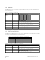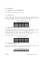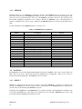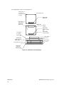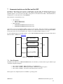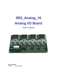
1
SPM186420 SPM176430 SPM176431 dspModule User’s Manual Utilizing the Power of the Texas Instrument TMS320C6416 DSP BDM-610030005 Rev. A SPM1x64xx dspModule User’s Manual RTD EMBEDDED TECHNOLOGIES, INC. 103 Innovation Blvd State College, PA 16803-0906 Phone: +1-814-234-8087 FAX: +1-814-234-5218 E-mail [email protected] [email protected] Web site http://www.rtd.com Manual Revision History Rev A) Initial Release – Based on BDM-610030004 Rev B. Added SPM176431 information. Published by: RTD Embedded Technologies, Inc. 103 Innovation Boulevard State College, PA 16803 Copyright 2006 by Real Time Devices, Inc. All rights reserved Printed in U.S.A. The RTD Embedded Technologies Logo is a registered trademark of RTD Embedded Technologies. dspModule, cpuModule, and utilityModule are trademarks of RTD Embedded Technologies. PC/104, PC/104Plus, and PCI_104 are registered trademark of PC/104 Consortium. TMS320C64x, VelociTI, and C64x are trademarks of Texas Instruments. All other trademarks appearing in this document are the property of their respective owners. 1 OVERVIEW .................................................................................................................................................2 1.1 1.2 1.3 2 HARDWARE INSTALLATION.................................................................................................................7 2.1 2.2 2.2.1 2.2.2 2.2.3 2.3 2.3.1 2.3.2 2.3.3 2.3.4 2.3.5 2.3.6 2.3.7 2.3.8 3 WHEN YOU NEED HELP ............................................................................................................2 DSP FEATURES .......................................................................................................................2 BOARD FEATURES ...................................................................................................................4 CONNECTING THE DSPMODULE ...............................................................................................7 SWITCH CONFIGURATIONS ......................................................................................................9 PCI Configuration Options ....................................................................................................9 SPM176430 ..........................................................................................................................10 SPM176431 and SPM186420 ..............................................................................................10 I/O CONNECTORS ..................................................................................................................11 PlatformBus – CN1, CN2 (SPM186420 only) ......................................................................11 SyncBus – CN4 .....................................................................................................................11 McBSP - Multi-channel Buffered Serial Port (CN5, CN6, CN7) .........................................11 JTAG Emulator Connector - CN9 ........................................................................................11 Power Connector – CN8 ......................................................................................................12 aDIO – Advanced Digital I/O (CN5) (SPM176431 Only)....................................................12 COM – RS-232/422/485 Serial Ports (CN13 & CN14) (SPM176431 Only) ........................12 Audio – AC97 Audio Input and Output (CN12) (SPM176431 Only) ...................................13 HARDWARE DESCRIPTION .................................................................................................................14 3.1 3.2 3.3 3.3.1 3.3.2 3.3.3 3.3.4 3.4 3.4.1 3.5 3.5.1 3.5.2 3.6 3.7 3.8 3.8.1 3.8.2 3.9 3.10 3.11 3.11.1 3.11.2 3.11.3 3.12 3.12.1 3.12.2 3.12.3 3.13 OTHER DOCUMENTS .............................................................................................................14 CLOCKING .............................................................................................................................14 PCI INTERFACE .....................................................................................................................15 Memory Regions...................................................................................................................15 PCI Interrupts ......................................................................................................................15 Doorbell & Mailbox Registers .............................................................................................15 EEPROM..............................................................................................................................16 SERIAL PORTS .......................................................................................................................16 McBSP 2...............................................................................................................................16 FLASH MEMORY ...................................................................................................................17 Memory Regions...................................................................................................................17 Booting .................................................................................................................................17 SYNCBUS (SPM176430 AND SPM186420 ONLY).................................................................17 RESET STRUCTURE ................................................................................................................18 WATCHDOG TIMERS..............................................................................................................19 Watchdog Timer A................................................................................................................19 Watchdog Timer B................................................................................................................19 INTERRUPTS ..........................................................................................................................19 PROCESSOR SPEED DETECTION .............................................................................................20 RS-232/422/485 SERIAL PORTS (SPM176431 ONLY)...........................................................20 Serial Port UART .................................................................................................................20 RS-232 Mode........................................................................................................................20 RS422 or RS485 Serial Port.................................................................................................20 ADIO (SPM176431 ONLY)...................................................................................................21 Internal Architecture ............................................................................................................21 Advanced Interrupts .............................................................................................................21 Interrupt De-bounce.............................................................................................................22 AC97 AUDIO (SPM176431 ONLY) .......................................................................................22 3.13.1 3.13.2 3.13.3 4 INTERFACING I/O SYSTEM VIA THE PLATFORMBUS (SPM186420 ONLY) ............................24 4.1 4.2 4.3 4.4 4.5 4.6 5 Control Data ........................................................................................................................22 Audio Data ...........................................................................................................................23 AC97 Initialization ...............................................................................................................23 THE PLATFORMBUS ..............................................................................................................24 EMIF TO PLATFORMBUS BRIDGE .........................................................................................24 CHANGING THE PLATFORMBUS CLOCK RATE .......................................................................24 PLATFORMBUS SIGNAL DESCRIPTION ...................................................................................24 PLATFORMBUS TIMING DIAGRAMS .......................................................................................27 PLATFORMBUS/EXTERNAL I/O BOARD MECHANICAL DIMENSIONS ........................................28 SPM1X64XX MEMORY MAP.................................................................................................................31 5.1 5.2 5.2.1 5.2.1.1 5.2.1.2 5.2.1.3 5.2.1.4 5.2.1.5 5.2.1.6 5.2.1.7 5.2.1.8 5.2.1.9 5.2.1.10 5.2.1.11 5.2.1.12 5.2.1.13 5.2.1.14 5.2.1.15 5.2.1.16 5.2.1.17 5.2.1.18 5.2.1.19 5.2.1.20 5.2.1.21 5.2.1.22 5.2.1.23 5.2.1.24 5.2.1.25 5.2.1.26 5.2.1.27 5.2.1.28 5.2.1.29 5.2.1.30 5.2.1.31 5.2.1.32 5.2.1.33 5.2.1.34 5.2.1.35 5.2.1.36 5.2.1.37 5.2.1.38 5.2.1.39 UART REGISTERS .................................................................................................................31 FPGA REGISTERS .................................................................................................................32 Register Descriptions ...........................................................................................................34 FPGA_SYNC_n_SEL (SPM176430 and SPM186420 only) .............................................................. 34 FPGA_SYNC_n_OEN (SPM176430 and SPM186420 only)............................................................. 35 FPGA_SYNC_n_GEN (SPM176430 and SPM186420 only) ............................................................. 35 FPGA_SWITCH_READ ..................................................................................................................... 35 FPGA_WDT_ENABLE....................................................................................................................... 36 FPGA_WDT_REFRESH..................................................................................................................... 36 FPGA_NMI ......................................................................................................................................... 37 FPGA_DSP_RESET............................................................................................................................ 37 FPGA_BOOTMODE........................................................................................................................... 37 FPGA_MCBSP_CON ......................................................................................................................... 38 FPGA_DSP_TIME0_SEL, FPGA_DSP_TIME1_SEL, FPGA_DSP_TIME2_SEL........................... 38 FPGA_PB_TIME0_SEL, FPGA_PB_TIME1_SEL (SPM186420 only) ............................................ 39 FPGA_DSP_GPIO0_SEL, FPGA_DSP_GPIO1_SEL, FPGA_DSP_GPIO2_SEL, FPGA_DSP_GPIO3_SEL................................................................................................................... 39 FPGA_LED ......................................................................................................................................... 39 FPGA_PCI_INT_STAT ...................................................................................................................... 40 FPGA_PCI_INT_ENA ........................................................................................................................ 40 FPGA_PB_CON_0 (SPM186420 only) .............................................................................................. 40 FPGA_PB_CON_1 (SPM186420 only) .............................................................................................. 41 FPGA_INT_STAT_L (SPM176430)................................................................................................... 41 FPGA_INT_STAT_L (SPM176431)................................................................................................... 42 FPGA_INT_STAT_L (SPM186420)................................................................................................... 44 FPGA_INT4_ENA_L, FPGA_INT5_ENA_L, FPGA_INT6_ENA_L, FPGA_INT7_ENA_L........... 45 FPGA_MAIL_0_L, FPGA_MAIL_0_H, FPGA_MAIL_1_L, FPGA_MAIL_1_H, FPGA_MAIL_2_L, FPGA_MAIL_2_H, FPGA_MAIL_3_L, FPGA_MAIL_3_H ............................................................ 45 FPGA_DOOR_P_S_L, FPGA_DOOR_P_S_H .................................................................................. 45 FPGA_DOOR_P_C_L, FPGA_DOOR_P_C_H.................................................................................. 46 FPGA_DOOR_D_S_L, FPGA_DOOR_D_S_H ................................................................................. 46 FPGA_DOOR_P_C_L, FPGA_DOOR_P_C_H.................................................................................. 47 FPGA_STATUS .................................................................................................................................. 47 FPGA_SCRATCH_0, FPGA_SCRATCH_1, FPGA_SCRATCH_2 .................................................. 48 FPGA_DSP_SPEED ........................................................................................................................... 48 FPGA_VERSION................................................................................................................................ 48 FPGA_ADIO_INOUT (SPM176431 Only) ........................................................................................ 49 FPGA_ADIO_DIR (SPM176431 Only).............................................................................................. 49 FPGA_ADIO_ENABLE (SPM176431 Only) ..................................................................................... 49 FPGA_ADIO_INT_MODE (SPM176431 Only) ................................................................................ 49 FPGA_ADIO_MASK (SPM176431 Only) ......................................................................................... 50 FPGA_ADIO_COMP (SPM176431 Only) ......................................................................................... 50 FPGA_ADIO_CAPT (SPM176431 Only)........................................................................................... 50 FPGA_COM_MODE (SPM176431 Only).......................................................................................... 51 5.2.1.40 5.2.1.41 5.2.1.42 5.2.1.43 5.2.1.44 6 INITIALIZATION OF THE SPM1X64XX .............................................................................................53 6.1 6.2 7 INTERNAL PERIPHERAL BUS EMIF REGISTER .........................................................................53 EMIF REGISTER DESCRIPTIONS .............................................................................................54 COMMUNICATION BETWEEN THE HOST AND THE DSP............................................................55 7.1 7.2 7.2.1 7.2.1.1 7.2.1.2 7.2.1.3 7.2.2 7.2.2.1 7.2.2.2 7.2.2.3 7.3 8 FPGA_AUDIO_MODE (SPM176431 Only) ...................................................................................... 51 FPGA_AC97_COMMAND_STAT (SPM176431 Only) .................................................................... 51 FPGA_AC97_WR_DATA (SPM176431 Only).................................................................................. 52 FPGA_AC97_RD_DATA (SPM176431 Only)................................................................................... 52 FPGA_AC97_McBSP_ENA (SPM176431 Only)............................................................................... 52 SLAVE TRANSFERS ................................................................................................................55 MASTER TRANSFERS .............................................................................................................56 Control Registers..................................................................................................................56 DSPMA ............................................................................................................................................... 56 PCIMA ................................................................................................................................................ 56 PCIMC................................................................................................................................................. 57 Monitor Registers .................................................................................................................57 CDSPA ................................................................................................................................................ 57 CPCIA ................................................................................................................................................. 57 CCNT .................................................................................................................................................. 57 PCI MASTER / TARGET MODES .............................................................................................58 INTERRUPTS ............................................................................................................................................59 8.1 8.2 8.3 EXTERNAL INTERRUPT OF THE DSP ......................................................................................59 INTERRUPTS FROM THE HOST TO THE DSP............................................................................59 INTERRUPTS FROM THE DSP TO THE HOST............................................................................59 APPENDIX A: LIMITED WARRANTY.........................................................................................................60 1 Overview The PCI-104 SPM186420 and the PC/104-Plus SPM17643x are high-performance DSP boards that are configurable to be either bus mastering or target only on the PCI bus. The SPM186420 has a PCI connector, an 80 pin DSP Platform Bus connector, and 3 high-speed (max. 75Mbit/s) 5V compliant Multi-channel Buffered Serial Ports (McBSPs). The Platform Bus and McBSPs allow easy connection to high-speed analog or other front-end modules without tying up the PCI bus. The SPM176430 is a PC/104-Plus board that has a PCI connector, an ISA connector, and 3 high-speed (max. 75Mbit/s) 5V compliant McBSPs. The SPM176431 is a PC/104-Plus board that has a PCI connector, an ISA connector, and 1 high-speed (max. 75Mbit/s) 5V compliant McBSPs, and AC97 Audio interface, and 2 RS-232/422/485 serial ports. 1.1 When you need help This manual and all the example programs will provide you with enough information to fully utilize all the features on this board. If you have any problems installing or using this board, contact our Technical Support Department (814) 234-8087 during EST business hours, or send an Email to [email protected]. When sending an Email request, please include your company's name and address, your name, your telephone number, and a brief description of the problem. 1.2 DSP Features The heart of the board is the very high performance Texas Instruments TMS320C6416 DSP. The main features of the DSP chip include: • • • • • High-Performance Fixed-Point Digital Signal Processors (DSP) TMS320C6416 − 500/600/1000 - MHz Clock Rate − 2/1.67/1 - ns Instruction Cycle Time − Eight 32-Bit Instructions/Cycle − 4000/4800/8000 MIPS − Fully Software-Compatible With C62x (including SPM6020 and SPM6030) VelociTI.2 Advanced Very Long Instruction Word (VLIW) C64x DSP Core − Eight Highly Independent Functional Units With VelociTI.2 Extentions: − Six ALUs (32-/40-Bit) − Two 16-Bit Multipliers (32-Bit Result) − Load-Store Architecture With 64 32-Bit General-Purpose Registers − Instruction Packing Reduces Code Size − All Instructions Conditional Instruction Set Features − Byte-Addressable (8-, 16-, 32-Bit Data) − 32-Bit Address Range − 8-Bit Overflow Protection − Bit-Field Extract, Set, Clear − Bit-Counting − Normalization − VelociTI.2 Increased Orthogonally Viterbi Decoder Coprocessor (VCP) − Supports Over 500 7.95-Kbps AMR − Programmable Code Parameters Turbo Decoder Coprocessor (TCP) SPM186420/176430 2 RTD Embedded Technologies, Inc. • • • • • • • • • − Supports up to Six 2-Mbps 3GPP (6 Iterations) − Programmable Turbo Code and Decoding Parameters L1/L2 Memory Architecture − 128 k-Bit (16 kB) L1P Cache (Direct-Mapped) − 128 k-Bit (16 kB) L1D Cache (2-Way Set-Associative) − 8 M-Bit (1MB) L2 Unified Mapped RAM/Cache (Flexible Allocation) Two External Memory Interfaces (EMIFs) − One 64 Bit (EMIFA) for SDRAM − One 16 Bit (EMIFB) for Flash and PlatformBus − Separation prevents slower accesses from delaying SDRAM operations Enhanced Direct-Memory-Access (EDMA) Controller (64 Independent Channels) 32-Bit/33-MHz, PCI Master/Slave Interface Conforms to PCI Specification 2.2 − Three PCI Bus Address Ranges: Prefetchable Memory, Non-Prefetchable Memory, I/O − Four-Wire Serial EEPROM Interface − PCI Interrupt Request Under PCI Control − DSP Interrupt Via PIC I/O or Memory Cycle Three Multi-channel Buffered Serial Ports (McBSPs) − Direct Interface to T1/E1, MVIP, SCSA Framers − ST-Bus-Switching, AC97 Compatible − Up to 256 Channels Each − Serial-Peripheral Interface (SPI) Compatible (Motorola) Three 32-Bit General-Purpose Timers IEEE-1149.1 (JTAG) Boundary-Scan-Compatible 0.12-µm/6-Level Metal Process − CMOS Technology 3.3-V I/Os SPM1x64xx RTD Embedded Technologies, Inc. 3 1.3 Board Features The SPM1x64xx boards use all of the above listed DSP chip features on a very small PCI-104 and PC/104-Plus form factor respectively. The board also includes the following features: • • • • • • • • • • • Up to 128 MB of Synchronous SDRAM with 800 MB/s transfer rate (256 MB available) 2 MB bootable FLASH for storing application programs (4 MB available) Two stage Watch Dog Timer On-Board 3.3V and Core Voltage Generation 3.3V signaling, 5V compliant PCI Interface SyncBus for synchronous operation with RTD’s high performance PC/104-Plus Data Acquisition dataModules or other types of analog interfaces. Three high-speed (max. 75Mbits/s) Multi-channel Buffered Serial Ports (T1/E1, MVIP, SCSA, ST bus, AC97 SPI Compatible) Platform Bus on the PCI-104 SPM186420 for dedicated high-speed DSP connection Power Connector to power the dspModule and any attached modules Doorbell and Mailbox registers to communicate between the PCI bus and the DSP DSP to PlatformBus bridge to maximize transfer efficiency between the 32-bit PlatformBus and 16-bit EMIFB Serial Port Clock circuit 41.67/50/60MHz Serial Port PCI bus DSP TMS320C6416 Serial Port PCI Bus interface Watch Dog Timer External Memory Interface SDRAM Asynchronous SDRAM 128MB Control Logic PlatformBus PlatformBus interface Flash 2/4MB 100 MHz SyncBus interface To other RTD boards with SyncBus Figure 1.1: Block diagram of SPM186420 The SPM186420 is labeled as a DSP accelerator while the SPM176430 is labeled as a DSP coprocessor board. Though we use different names, both boards can be used as either a coprocessor or as a high-speed accelerator to an analog front-end module. If the application needs an analog interface, the PlatformBus (which is actually the asynchronous interface of the DSP – SPM186420 only) can be used for easy, direct, high-speed data transfers SPM1x64xx 4 RTD Embedded Technologies, Inc. between the DSP and the analog interface without tying up the PCI bus. The other possibility of interfacing the analog front-end directly to the DSP without tying up the PCI bus is through the three high-speed McBSPs. Clock generator 41.67/50/60MHz PCI bus DSP TMS320C6414 Serial Port McBSP0 Serial Port McBSP1 Serial Port McBSP2 PCI Bus interface Watch Dog Timer External Memory Interface SDRAM Asynchronous SDRAM 128MB Control Logic ISA bus Power connection from ISA bus Flash 2/4 MB 100 MHz SyncBus interface To other RTD boards with SyncBus Figure 1.2: Block diagram of SPM176430 SPM1x64xx RTD Embedded Technologies, Inc. 5 McBSP1 AC97 CODEC McBSP0 Serial Port Clock generator 41.67/50/60MHz PCI bus DSP TMS320C6414 ISA bus Power connection from ISA bus External Memory Interface SDRAM Asynchronous Dual UART SDRAM 128/256MB Control Logic McBSP/ aDIO aDIO PCI Bus interface Watch Dog Timer Audio RS-232/ 422/485 Flash 2 MB 100 MHz Figure 1.3: Block diagram of SPM176431 When the ROM Boot Switch is off, the system after power up is in the RESET state waiting for the loading of a program to the on-chip memory via the PCI bus interface. All of the memory resources of the DSP can be accessed from the PCI bus. Thus, the memory at zero address – on-chip RAM – can be accessed. After loading the program into the memory at address zero, you can start the program operation using the DSPINT command that wakes up the DSP from RESET. When the ROM Boot switch is on you can use the Flash memory as a boot device. Flash can be programmed from the DSP or from the PCI bus. A watch dog timer can be used as an automatic RESET generator in critical applications. It can be used with the Flash memory boot. Data transfer over the PCI bus and the DSP can be done by several methods: • Host CPU as a PCI bus master: CPU can directly access the DSP’s internal memory, or the DSP’s external memory, or the memory off of the Platform bus without using DSP resources. • DMA controller inside DSP chip as a PCI master: DSP and CPU resources are not used. • External device as a PCI bus master The external device can directly access the DSP’s internal memory, or the DSP’s external memory, or the memory off of the Platform bus without using DSP resources. There are Interrupt connections between the DSP and Host CPU that allow each of them to interrupt the other. SPM1x64xx 6 RTD Embedded Technologies, Inc. 2 2.1 Hardware Installation Connecting the dspModule The SPM1x64xx is designed for PCI-104 / PC/104-Plus systems. To install the board you need to do the following steps (See Figures below): • • • • • • • Make sure, that your PCI-104 or PC/104-Plus system is powered off Use electrostatic wrist strap Set the slot selection switch to the proper position. (See Section 7.3) Turn on the “PCI Master” switch if you want to use the SPM186420 / 176430 as bus master on the PCI bus. Set the “ROM Boot” switch to the proper position according to the needed boot mode Connect push-button to JP4, or use a jumper to reset the DSP and PlatformBus. - Optional Insert your card into your system PCI bus connector JP4 –Reset: short – DSP / PlatfomBus in Reset open – After Reset pulse generation Reset line inactive High state SW2 – Master /Target, Boot Mode: 1: PCI Master 2: ROM Boot 3: Flash Write 4: Four Master CN4 - SyncBus Connector SPM186420 CN5 - McBSP 0 serial port connector CN6 - McBSP 1 serial port connector CN11-LED Connector CN7 - McBSP 2 serial port connector Platform Bus connector CN8-Power Connector CN9- JTAG Connector SW2 – Slot selection Switch CN10 – Xilinx Programming Figure 2.1: SPM186420 Connector Locations SPM1x64xx RTD Embedded Technologies, Inc. 7 SW1 – PCI Options 1: Slot Selection [0] 2: Slot Selection [1] 3: PCI Master 4: Four Master PCI bus connector JP4 –Reset: short – DSP in Reset open – After Reset pulse generation Reset line inactive High state SW2 – DSP Options 1: ROM Boot 2: Flash Write 3: User Switch 3 4: User Switch 4 CN4 - SyncBus Connector SPM176430 CN5 - McBSP 0 serial port connector CN6 - McBSP 1 serial port connector CN11-LED Connector CN7 - McBSP 2 serial port connector ISA Bus connector CN8-Power Connector CN9- JTAG Connector CN10 – Xilinx Programming Figure 2.2: SPM176430 Connector Locations SPM1x64xx 8 RTD Embedded Technologies, Inc. PCI bus connector SW2 – Master /Target, Boot Mode: 1: PCI Master 2: ROM Boot 3: Flash Write 4: Four Master JP4 –Reset: short – DSP in Reset open – DSP operational CN13 – COM1 RS232/422/485 SPM176430 CN5 - McBSP 0 / aDIO CN14 - COM2 RS232/422/485 CN11-LED Connector CN12 - Audio port ISA Bus connector CN8-Power Connector CN9- JTAG Connector SW1 – Slot selection Switch Figure 2.3: SPM176431 Connector Locations 2.2 2.2.1 Switch Configurations PCI Configuration Options To install the dspModule into the stack, the PCI Slot Number must be configured correctly. This is done by the PCI Slot Selector located at SW1. There are four possible PCI Slot Numbers (0 – 3). Each PCI device (PC/104-Plus or PCI-104) must a use a different slot number. The slot number is related to the position of the board in the stack. Slot 0 represents the PCI device closest to the CPU. Slot 3 represents the PCI devices farthest away from the CPU. Note: In a PC/104-Plus or PCI-104 system, all PCI devices should be located on one side of the CPU board (above or below the add-on cards). The CPU should not be located between two PCI devices. When the PC/104-Plus Specification was first introduced, it only allowed for three PCI add-on cards to be bus masters. The cards in slot 2 and 3 shared arbitration signals (REQ# and GNT#), and only one could be configured as a master. Version 2.0 of the PC/104-Plus specification was released in November 2003. This version of the specification adds support for all 4 PCI slots to be bus masters. In order to provide compatibility with the original specification, a “4 Master” switch is provided. SPM1x64xx RTD Embedded Technologies, Inc. 9 2.2.2 SPM176430 The SPM176430 provides a set of switches to configure the PCI slot and other options. The switch definitions are shown in the table below: Table 2.1: Switch Definitions (SPM176430) Switch Name Description SW1-1 Slot Selects the PCI Slot as follows: SW1-2 SW1-2 SW1-1 PCI Slot OFF OFF 0 OFF ON 1 ON OFF 2 ON ON 3 SW1-3 PCI Master ON = PCI Master Enabled OFF = PCI Target Only SW1-4 4 Master ON = Enabled 4 masters on the PCI bus OFF = Slot 2 and 3 share arbitration signals SW2-1 ROM Boot ON = Boot from on-board flash OFF = Wait for code to be loaded from PCI bus SW2-2 Flash Wrt ON = Enable writing to flash OFF = Disable writing to flash SW2-3 User Switch 3 Read from FPGA_SWITCH_READ SW2-4 User Switch 4 Read from FPGA_SWITCH_READ 2.2.3 SPM176431 and SPM186420 The SPM176431 and SPM186420 provide a rotary switch to configure the PCI slot, and toggle switches to configure other options. The switch definitions are shown in the tables below: Table 2.2:Rotary Switch Definitions (SPM176431 and SPM186420) Switch Position Description 0 Slot 0 (Closest to CPU) 1 Slot 1 2 Slot 2 3 Slot 3 (Farthest from CPU) others Reserved Table 2.3: Switch Definitions (SPM176431 and SPM186420) Switch Name Description SW2-1 PCI Master ON = PCI Master Enabled OFF = PCI Target Only SW2-2 ROM Boot ON = Boot from on-board flash OFF = Wait for code to be loaded from PCI bus SW2-3 Flash Wrt ON = Enable writing to flash OFF = Disable writing to flash SW2-4 4 Master ON = Enabled 4 masters on the PCI bus OFF = Slot 2 and 3 share arbitration signals SPM1x64xx 10 RTD Embedded Technologies, Inc. 2.3 2.3.1 I/O Connectors PlatformBus – CN1, CN2 (SPM186420 only) The Platform Bus connector is described in Section 4 on page 24. 2.3.2 SyncBus – CN4 The SyncBus is an RTD defined bus for synchronous operation with other RTD’s boards. The SyncBus connector is the CN3 Connector at the right top corner of the board. The SyncBus is a TTL signaling level and 5V compliant tristate bus. The SyncBus can be used to trigger an analog front-end, or to receive signaling. Table 2.4: syncBus Pin Assignments SyncBus0 GND SyncBus1 GND SyncBus2 2.3.3 1 3 5 7 9 2 4 6 8 10 GND GND GND GND GND McBSP - Multi-channel Buffered Serial Port (CN5, CN6, CN7) The SPM186420/176430 contains three max 75Mbit/s data rate 5V compliant McBSP serial buses to interface a front-end to the DSP. The CN5, CN6, and CN7 are the connectors of McBSP0, 1, and 2 respectively. The SPM176431 contains one max 75Mbit/s data rate 5V compliant McBSP serial buses to interface a front-end to the DSP. The CN5 connector is the connector to McBSP0, and can also be configured as aDIO. The pin-out of the McBSP ports (identical for all serial ports) is show in Table 2.5. Table 2.5: McBSP Pin Assignments CLKS CLKR CLKX DR DX 2.3.4 1 3 5 7 9 2 4 6 8 10 GND FSR GND FSX GND JTAG Emulator Connector - CN9 Using this connector the SPM1x64xx can be debugged by JTAG emulator hardware supplied by several manufacturers. It is compatible with Spectrum Digital XDS510 emulator with 3V cable. Table 2.6: JTAG Emulator Pin Assignments TMS SPM1x64xx 1 2 TRST RTD Embedded Technologies, Inc. 11 TDI +3.3V TDO TCK TCK EMU0 2.3.5 3 5 7 9 11 13 4 6 8 10 12 14 GND Key GND GND GND EMU1 Power Connector – CN8 The SPM1x64xx can be powered externally using this connector. The +5V power is the only one used on this board. The +12V, –12V, and +3.3V power is used to supply the PlatformBus, ISA bus, and PCI bus. This connector can also be used to power external devices. Table 2.7: Power Connector Pin Assignments GND No Connection No Connection GND GND n.c. 2.3.6 1 3 5 7 9 11 2 4 6 8 10 12 +5V +12V -12V +5V +3.3V +3.3V aDIO – Advanced Digital I/O (CN5) (SPM176431 Only) The pin-out of the aDIO ports is show in Table 2.8. Table 2.8: aDIO Pin Assignments aDIO[6] aDIO[5] aDIO[3] aDIO[2] aDIO[0] 2.3.7 1 3 5 7 9 2 4 6 8 10 GND aDIO[4] GND aDIO[1] GND COM – RS-232/422/485 Serial Ports (CN13 & CN14) (SPM176431 Only) Two standard PC serial ports are provided that can be configured as RS-232/422/485. When in RS-422/485 mode, the RTS signal controls the enable for the drivers. The pin assignments for RS-232 mode are shown in Table 2.9 , and the pin assignments for RS-422/485 mode are shown in Table 2.10. Table 2.9: RS-232 Pin Assignments DCD RXD TXD DTR GND 1 3 5 7 9 2 4 6 8 10 DSR RTS CTS RI GND Table 2.10: RS-422/485 Pin Assignments Reserved RXD- SPM1x64xx 12 1 3 2 4 Reserved TXD+ RTD Embedded Technologies, Inc. TXDReserved GND 2.3.8 5 7 9 6 8 10 RXD+ RI GND Audio – AC97 Audio Input and Output (CN12) (SPM176431 Only) The pin-out of the Audio port is show in Table 2.11. The audio output can be selected as either Line level or Headphone level. Line level is 1VRMS nominal. A bias voltage (MIC_VREF) provides 2.2V at 5mA to bias a microphone. The line inputs use a pseudo-differential input; the LINE_IN_GND must be connected to the ground of the line input source. Table 2.11: Audio Pin Assignments MIC_VREF GND LINE_IN_GND GND GND SPM1x64xx 1 3 5 7 9 2 4 6 8 10 MIC_IN LINE_IN_LEFT LINE_IN_RIGHT OUTPUT_LEFT OUTPUT_RIGHT RTD Embedded Technologies, Inc. 13 3 3.1 Hardware Description Other Documents The TMS320C6416 Digital Signal Processor is a very complex device. A full description of its internal functions and registers is beyond the scope of this document. Full documentation is supplied by Texas Instruments. TI also supplies application notes to demonstrate many of the functions of this DSP. For more information, search TI’s website (www.ti.com) for the phrase “TMS320C6416.” Of particular interest is the “TMS320C6000 Peripherals Overview.” This document from TI gives a brief description of all of the on-chip peripherals, and provides link for detailed manuals of each. This includes the PCI interface, Serial Ports, Timer/Counters, DMA engine, and many other things. The Texas Instruments internal document number is SPRU190. This document covers several devices from the C6000 family, so care should be taken to insure the correct information is being used. This document will focus on the features that are unique to the SPM1x64xx. 3.2 Clocking The core / peripheral clocking source and the EMIFx clocking source are independent of each other. Figure 3.1 shows the clocking options of the SPM1x64xx board: Figure 3.1: SPM1x64xx onboard clocking SPM1x64xx 14 RTD Embedded Technologies, Inc. 3.3 PCI Interface The DSP can communicate directly with the PCI bus. It is capable of responding to memory and I/O cycles. It is also capable of generating memory, I/O, and configuration cycles. In order for the PCI interface to operate, a cpuModule must also be present in the stack. The cpuModule provides PCI clocks and arbitration. The cpuModule also configures the PCI bus. The SPM1x64xx is not capable of generating PCI clocks, and also cannot generate arbitration signals. Furthermore, the PCI interface of the DSP must be configured by an external master before it can configure other modules. After the PCI bus is configured, the SPM1x64xx is fully capable of accessing any resources on the PCI bus. This includes system memory, video cards, hard drives, etc. 3.3.1 Memory Regions The SPM1x64xx appears on the PCI bus as three Base Address Registers, BAR0 through BAR2. BAR0 is a 4 MByte, memory mapped window into the DSP’s internal address space. The window is set through the DSP Page register. BAR1 is an 8M-Byte, memory mapped window into the DSP’s internal registers. It is permanently set to start at address 0x0180:0000. BAR2 is a set of I/O mapped registers. They include the DSP Page register, and reset and interrupt controls. 3.3.2 PCI Interrupts There are two sources for generating PCI interrupts from the DSP. The first is the PCI interface itself. An interrupt can be generated by setting a bit in the DSP reset/source register. It is then cleared on the PCI side by writing to a bit in PCI registers (in either BAR1 or BAR2). The second source of PCI interrupts is the DSP-to-PCI Doorbell register. The DSP generates an interrupt by setting one of the bits in the DSP-to-PCI Doorbell register. The PCI side can then clear the bit to clear the interrupt. PCI interrupts must be enabled before they can be asserted. The appropriate interrupt must first be enabled in the FPGA_PCIINTEN register. Also, to enable the PCI interface interrupt, the HSR [INTAM] bit must be cleared. 3.3.3 Doorbell & Mailbox Registers A set of Doorbell and Mailbox Registers are provided to aid in the communication between the DSP and the PCI host. The doorbell registers generate an interrupt when any bit is set. Bits are set by writing a ‘1’ to the appropriate location in a set register. Bits are cleared by writing a ‘1’ to the appropriate location in a clear register. Reading from either location returns the value of the doorbell register. There are two doorbell registers; the DSP-to-PCI Doorbell generates a PCI interrupt, and the PCI-to-DSP Doorbell generates a DSP interrupt. The Mailbox Registers generate an interrupt when they are written to. There are four Mailbox registers, all of which can generate a DSP interrupt. The Mailbox Register cannot determine if it is being accessed by the PCI host or by the DSP. It will generate an interrupt any time it is written to. Therefore, the DSP must disable the Mailbox interrupt whenever it modifies the Mailbox Register. SPM1x64xx RTD Embedded Technologies, Inc. 15 3.3.4 EEPROM The PCI interface uses an EEPROM to identify the module. This EEPROM can also be used to store user information. The total size of the EEPROM is 256 Words. The first 13 words are used for PCI configuration. The next 19 are used for system information. The reset of the EEPROM is available for the user. The user must ensure that the PCI configuration information is not corrupted. Because the EEPROM is part of the PCI interface, it requires a valid PCI reset in order to operate. Therefore, the EEPROM should not be used in systems without a host CPU. For more information on the EEPROM interface, see Section 3.4.1. Table 3.1: EEPROM Word Assignments Address 0x00 0x01 0x02 0x03 0x04 0x05 0x06 0x07 0x08 0x09 0x0A 0x0B 0x0C 0x0D 0x0E 0x0F 0x10 0x11 – 0x1F 0x20 – 0xFF 3.4 Description Vendor ID Device ID Class Code[7..0]/Revision ID Class Code[23..8] Subsystem Vendor ID Subsystem ID Max Latency / Min Grant PC_D1 / PC_D0 (power consumed D1, D0) PC_D3 / PC_D2 (power consumed D3, D2) PC_D1 / PC_D0 (power dissipated D1, D0) PC_D3 / PC_D2 (power dissipated D3, D2) Data_scale (PD_D3..PC_D0) 0000 0000 PMC[14..9], PMC[5], PMC[3] Checksum Nominal Speed Flash SDRAM Reserved for system information User EEPROM Area Default 0x1435 0x6420 / 0x6430 0x00FF 0x0B40 0x104C 0xA106 0x0000 0x0000 0x0000 0x0000 0x0000 0x0000 0x0000 {CheckSum} {DSP Speed} {Flash Size} {SDRAM Size} Reserved Serial Ports The SPM1x64xx provides three Multi-Channel Buffered Serial Ports (McBSP). These ports connect directly the DSP. They can be used to transfer data between the dspModule and a dataModule. They can also be used to transfer data between dspModules. The McBSP ports are 5V tolerant. 3.4.1 McBSP 2 McBSP 2 is shared between the serial port connector and the PCI EEPROM. A switch is provided that can disconnect the McBSP port from the connector when it is being used for the EEPROM interface. This prevents external devices from interfering with EEPROM operations. Switching between McBSP mode and EEPROM mode is generally automatic. During DSP Reset or PCI Reset, the port is placed in McBSP mode. After either reset is negated, the port is switched to EEPROM mode for 5ms. The port is then switched to McBSP mode until the next reset. SPM1x64xx 16 RTD Embedded Technologies, Inc. The implication is that if McBSP 2 is being used when the Host system (PCI) resets, the DSP will temporarily lose communication with the device on McBSP 2. If this cannot be tolerated, the port can be “locked” to McBSP mode by writing the FPGA_MCBSP_CON register. However, if the host resets, the PCI interface of the DSP will be uninitialized, and will not be recognized by the driver. To use the EEPROM for user functions, the McBSP port must first be locked to EEPROM mode. This is done by writing the FPGA_MCBSP_CON register. See Section 5.1 for details. 3.5 Flash Memory Either 2MB or 4MB of flash memory is provided. This memory is designed to store DSP firmware. The Flash device is separated into several sectors. An entire sector must be erased at a time. A special procedure must be used to erase or program the flash. For detail, refer to the AM29LV320D (4 MB) or AM29LV160D (2MB) datasheet from AMD (www.amd.com). A write enable switch is provided on the SPM1x64xx. This is the third switch on SW2. When the switch is “on,” the Flash can be written to. When the switch is “off,” all write commands are disabled. NOTE: Disabling the write commands also disables the auto select command, which is used to identify the flash device. 3.5.1 Memory Regions There are two memory regions associated with the Flash Device. The region CE1 is located from 0x6400:0000 to 0x641F:FFFF. The region CE2 is located from 0x6800:0000 to 0x681F:FFFF. For the 4 MB Flash device, the lower sectors are mapped to CE1, and the upper sectors are mapped to CE2. For the 2 MB device, the entire device is mapped to both locations. Note that there are several images of CE1 repeated from 0x6400:0000 to 0x643F:FFFF, so the entire 4 MB flash device can be accessed from 0x6760:0000 to 0x681F:FFFF. 3.5.2 Booting There are two methods for booting the DSP. When the “Flash Boot” switch is turned off, the DSP will power up in an internal reset mode. The PCI interface is then used to load a program into the DSP. The DSPINT bit of the HDCR register is then set and the DSP will start executing from address 0x0000:0000. When the “Flash Boot” switch is turned on, the DSP will boot from flash. The first 1 kB from the CE1 memory region is transferred to internal memory at address 0x0000:0000. The DSP then begins executing from address 0x0000:0000. During flash boot, the DSP assumes that an 8 bit flash is used. However, the flash device on the SPM1x64xx is 16 bits wide. Therefore, to load a program into Flash, only the even bytes can be used. 3.6 SyncBus (SPM176430 and SPM186420 only) The SyncBus is a bus that synchronizes the operation of multiple SPM1x64xx or other boards. The source of signals can be from itself or from other boards. The signals driven on the SyncBus are generally a short pulse. The rising edge of the pulse signals a synchronization event. The synchronization events can generally be used for either periodic captures, or to start a capture sequence. SPM1x64xx RTD Embedded Technologies, Inc. 17 The SyncBus connector provides three channels. Each of these channels can be a master or a slave. When a channel is a master, it is driven by the SPM1x64xx. It can be driven by any of the three internal counter/timers, or by a memory write operation. When a channel is a slave, the synchronization events can cause an interrupt on any of the four interrupt pins, and can feed into any of the three counter/timers. The synchronization event can also be sent to the Tout pins of the PlatformBus (SPM186420 only). A channel can be both a master and a slave at the same time. SyncBus0 source SyncBus0 enable SyncBus1 source SyncBus1 enable SyncBus2 source SyncBus2 enable SyncBus to other boards SyncBus to other boards SyncBus0 buffered SyncBus1 buffered SyncBus2 buffered Figure 3.2: The SyncBus structure It is important, that a SyncBus signal can have only one enabled active buffer. See sections 5.2.1.1, 5.2.1.2 and 5.2.1.3 for register setup and description. 3.7 Reset Structure There are two separate reset domains on the SPM1x64xx. One is the PCI domain. Resets in this domain only control the registers that provide address decode on the PCI bus. The PCI reset generates a DSP interrupt. The other domain is the DSP reset. This domain has several levels of reset, which are summarized in Table 3.2. The PCI Reset is performed by resetting the host system. Warm Reset is performed by setting the WARMRESET bit of the HDCR register. FPGA_DSP_RESET is performed by writing to the FPGA_DSP_RESET register. The Watchdog Reset occurs when the watchdog timer is enabled and expires. Installing JP4 results in a Jumper Reset. A Power On Reset occurs when the power supply drops below a minimal level. SPM1x64xx 18 RTD Embedded Technologies, Inc. Table 3.2: Reset Summary Reset Type PCI Registers Reset DSP Registers FPGA Registers Reset Reset PCI Reset Yes No No Warm Reset No Yes No FPGA_DSP_RESET No Yes Yes* Watchdog B Reset No Yes Yes* Watchdog A Reset No Yes Yes Reset Jumper (JP4) No Yes Yes Power On Reset Yes Yes Yes * The Boot Mode Control register (FPGA_BOOTMODE) is not affected. FPGA Reloaded No No No No Yes Yes Yes See Section 3.4.1 for a description of McBSP port 2 during reset. 3.8 Watchdog Timers Two watchdog timers are provided to provide an interrupt and/or a reset if the DSP becomes non-functional. They may be used separately, or in conjunction with each other. 3.8.1 Watchdog Timer A Watchdog Timer A generates a reset after a fixed amount of time. It is a hardware device, and the reset that it generates is identical to the Reset Jumper. This watchdog is enabled by writing to the FPGA_WDT_ENABLE register. The watchdog will then generate a reset if it is not refreshed within 550 to 1650 ms. It is recommended that the watchdog be refreshed every 250 ms when in use. The watchdog is refreshed by writing to the FPGA_WDT_REFRESH register. The value of the write does not matter. 3.8.2 Watchdog Timer B Watchdog Timer B generates either a Non-Maskable Interrupt (NMI) or reset, and provides two choices for the timeout period. An NMI is the highest priority interrupt. The reset generated by Watchdog B is identical to writing to the FPGA_DSP_RESET register. This watchdog can be set to timeout at 336 ms or 5.3 seconds by setting a bit in the FPGA_WDT_ENABLE register. Setting Watchdog B to generate an interrupt at the shorter timeout and enabling Watchdog A provides a very robust system. If the system becomes non-functional, an NMI is generated which allows the DSP to attempt to recover. If it does not recover, the DSP will then reset. 3.9 Interrupts There are four external interrupts to the DSP, and one Non-Maskable Interrupt (NMI). An NMI is generated by writing 0xAA55 to the FPGA_NMI register, or by Watchdog timer B. The external interrupts are numbered 4 through 7. An interrupt can be generated from any combination of the sources listed in the FPGA_INT_STATUS_L register. An interrupt source is selected to an interrupt by writing a ‘1’ to the corresponding bit in the FPGA_INT_x_ENA_L register, where “x” is the interrupt number (4 to 7). The FPGA_INT_STATUS_L register is a sticky register. A bit is set to ‘1’ when an interrupt condition occurs. It will stay high until it is cleared by the DSP. A bit is cleared by writing a ‘1’ to it. The status register should always be cleared before enabling interrupts. SPM1x64xx RTD Embedded Technologies, Inc. 19 The external interrupts on the DSP are rising edge active. Therefore, it is possible for a missed interrupt to disable all subsequent interrupts. Consider a system in which Sync 0 Event and Sync 1 Event are both mapped to Interrupt 4. During the interrupt service routine (ISR) for Sync 0, a Sync 1 Event occurs. The ISR completes, clears the Sync 0 bit of the status register, and exits. However, Interrupt 4 is still high. The DSP does not detect this because a rising edge did not occur. Because Interrupt 4 remains high, any subsequent Sync 0 or Sync 1 events will not generate an interrupt. To avoid this condition, the ISR for Interrupt 4 must check the status of the interrupt pin before exiting. This is best done by reading the GPVAL register. If the interrupt is still high, the ISR must then be performed again to determine which interrupt is pending. This technique should be followed any time more than one interrupt source drives an interrupt pin. 3.10 Processor Speed Detection The processor speed is automatically detected after reset. The value is stored in the FPGA_DSP_SPEED register. This is the actual measured speed in MHz. It may vary up to +/- 2%, depending on power –up conditions. 3.11 RS-232/422/485 Serial Ports (SPM176431 Only) The two serial ports are implemented on connectors CN7 and CN8 respectively. Each port can be configured as a PC compatible full-duplex RS232 port, full-duplex RS422, or half-duplex RS485. 3.11.1 Serial Port UART The serial port is implemented with a 16550-compatible UART (Universal Asynchronous Receiver/Transmitter). This UART is capable of baud rates up to 115.2 kbaud in 16450 and 16550A compatible mode and up to 921.6 kbaud in extended mode. It includes a 16-byte FIFO. Please refer to the Exar XR16L2552 datasheet, found at www.exar.com for more detailed information. 3.11.2 RS-232 Mode The full-duplex RS232 mode is selected by setting FPGA_COM_MODE[COMn] = “10” for the appropriate serial port. With this mode enabled, the serial port connector must be connected to RS232 compatible devices. The pin assignment for RS-232 mode is found in Table 2.9 on page 12. 3.11.3 RS422 or RS485 Serial Port You may select RS-422/485 mode by setting FPGA_COM_MODE[COMn] = “11” for the appropriate serial port. In this case, you must connect the serial port to an RS422 or RS485 compatible device. The pin assignment for RS422/485 mode is found in Table 2.10 on page 12. When using RS422 or RS485 mode, you can use the port in either half-duplex (two-wire) or full duplex (four-wire) configurations. For half-duplex (2-wire) operation, you must connect RXD+ to TXD+, and connect RXD- to TXD-. A 120 ohm termination resistor is provided on the dspModule. Termination is usually necessary on all RS422 receivers and at the ends of the RS485 bus. If the termination resistor is required, it can be enabled by closing jumper JP1 for Serial Port 1, or JP2 for Serial Port 2. SPM1x64xx 20 RTD Embedded Technologies, Inc. When using the serial port in RS-422 or RS-485 mode, the serial transmitters are enabled and disabled under software control. The transmitters are enabled by manipulating the Request To Send (RTS*) signal of the serial port controller. This signal is controlled by writing bit 1 of the Modem Control Register (MCR) as follows: • • If MCR bit 1 = 1, then RTS* = 0, and serial transmitters are disabled If MCR bit 1 = 0, then RTS* = 1, and serial transmitters are enabled 3.12 aDIO (SPM176431 Only) The Advanced Digital Input/Output (aDIO) shares a connector with McBSP0 on the SPM176431. The connector is aDIO by default, and can be changed by writing to the FPGA_ADIO_ENABLE register found on page 49. 3.12.1 Internal Architecture A diagram of the standard I/O is shown in Figure 3.3. Each digital I/O pin can be individually configured as an input or output. Figure 3.3: Digital I/O Block Diagram 3.12.2 Advanced Interrupts An Advanced Interrupt block is provided that can generate an interrupt on a match or event. The match and event interrupts are across all 7 digital I/O. The bits can be individually selected. When an interrupt is generated, the data on all of the ports is latched into the Capture registers. Bits are tested regardless of whether a pin is an input or output. A Match interrupt is generated when the following expression is true for ALL bits (y): ((PORT[y] xor COMP[y]) and not MASK[y]) = ‘0’ SPM1x64xx RTD Embedded Technologies, Inc. 21 An Event interrupt is generated when the following expression is true for ANY ports (x) and bits (y). Note that the Capture register is updated at every interrupt or event: ((PORT[y] xor CAPT[y]) and not MASK[y]) = ‘1’ When changing interrupt modes, the mask register, or the compare register, the interrupt should first be disabled by setting FPGA_ADIO_INT_MODE to DISABLED. This will clear the de-bounce filter and prevent the loss of an interrupt, or a spurious interrupt. If the interrupt is left enabled, and the settings of the aDIO is changed from one set of conditions that cause an interrupt to another set of conditions that cause and interrupt before the de-bounce filter can react, the second interrupt will be lost. 3.12.3 Interrupt De-bounce A de-bounce filter is provided to prevent spurious interrupts. The de-bounce period can be set to 20ms or 40ns. An interrupt will not be generated unless the input is stable for the entire de-bounce period. The de-bounce filter is cleared when interrupts are disabled, and every time an Event interrupt is generated. 3.13 AC97 Audio (SPM176431 Only) The AC97 CODEC uses a 5-wire digital serial link, or "AC-Link", between the audio codec device and its digital controller. An AC’97 device can perform digital-to-analog conversion, analog-to-digital conversion, and analog input mixing. It supports different analog audio inputs/outputs and can communicate with a digital controller through the AC-Link. The AC-Link is attached to the on-board FPGA. The AC-Link provides for communication of both control data and audio data. In order to improve efficiency, control data and audio data are handled separately. The CODEC used on this board is the National Semiconductors LM4550A. Information on its capabilities and register set can be found at www.national.com. 3.13.1 Control Data The AC97 CODEC has several control registers that adjust the sample rate, volume, record input, etc. These are accessed through a set of registers in the FPGA. The registers are FPGA_AC97_COMMAND_STAT, FPGA_AC97_WR_DATA, and FPGA_AC97_RD_DATA. See section 5.2.1 on page 34 for more details. To write to a CODEC register: 1) Wait until FPGA_AC97_COMMAND_STAT[READY] = 1. 2) Write the data value to be written into FPGA_AC97_WR_DATA. 3) Write the address to be written to FPGA_AC97_COMMAND_STAT, also setting the READY bit and clearing the READ bit. This can be done in a single operation. 4) When FPGA_AC97_COMMAND_STAT[READY] = 1 the write has completed. (There is no need to wait for the READY bit to be set, as long as another CODEC read or write is not started). To read from a CODEC register: 1) Wait until FPGA_AC97_COMMAND_STAT[READY] = 1. 2) Write the address to be written to FPGA_AC97_COMMAND_STAT, also setting the READY bit and setting the READ bit. This can be done in a single operation. 3) Wait until FPGA_AC97_COMMAND_STAT[READY] = 1. 4) The register value can now be read from FPGA_AC97_RD_DATA. SPM1x64xx 22 RTD Embedded Technologies, Inc. 3.13.2 Audio Data Audio data from the CODEC is attached to McBSP1. A Transmit Frame Sync signal is provided to the DSP when output audio data is requested. A Receive Frame Sync signal is provided to the DSP when input audio data is available. When each frame sync is generated, two 32-bit elements are transferred: the first is for Left audio, the second is for Right audio. Each 32-bit element contains a left-justified 20-bit data element (MSB first) followed by 12 dummy bits. If 16-bit audio is desired, only access the upper word of the Data Receive Register (DRR) or Data Transmit Register (DXR). 3.13.3 AC97 Initialization The AC97 reset signal is attached to Timer Output 0. This must be set high by writing to CTL0 before accessing the control registers or attempting to send audio data. Because the Frame Syncs for McBSP1 are generated external to the DSP, care must be taken to ensure that the left and right channels are synchronized. If the McBSP transmitter is brought out of reset shortly before the Frame Sync arrives, the DSP or EDMA may not have a chance to service the Data Transmit Register. In that case, the transmitter shifts out the default value for the Left Audio data. When the Data Transmit Register is serviced, the Left Audio data is then shifted out in the time slot for the Right Audio data. The channels will continue to be swapped until the McBSP is restarted. This condition is avoided by using the FPGA_AC97_McBSP_ENA register as described below. The following procedure is recommended for initializing the audio interface: 1) Bring the AC97 CODEC out of reset by setting CTL0 = 0x00000004. 2) Initialize the AC97 CODEC registers as outlined in Section 3.13.1. 3) Verify that the AC97 McBSP interface is disabled (FPGA_AC97_McBSP_ENA[ENA] = 0). 4) Initialize and enable the EDMA channels that service McBSP1. 5) Initialize McBSP1 (RCR1 = 0x000101A0, XCR1 = 0x000101A0, PCR1 = 0x00000000). 6) Enable McBSP1 (SPCR1 = 0x02012001). 7) Enable the AC97 McBSP (FPGA_AC97_McBSP_ENA[ENA] = 1). Because there will be at least 20us before the first Frame Sync, there is guaranteed to be enough time for the EDMA to service McBSP1. SPM1x64xx RTD Embedded Technologies, Inc. 23 4 4.1 Interfacing I/O system via the PlatformBus (SPM186420 only) The PlatformBus The PlatformBus of the SPM186420 is the buffered version of the asynchronous External Memory Interface (EMIF) of the DSP. It is used to interface external analog or other type of I/O systems to the SPM186420. The Address range of this platform is 64 K long words or 256KB. The PlatformBus has 32bit wide data bus and uses a dedicated, programmable memory controller. The bus has a clock signal which can be used to synchronize the external device to the EMIF clock. This clock has a programmable rate and can be set to EMIF clock, EMIF clock/2 and EMIF clock/4. The signaling level of the PlatformBus is 3.3V. The bus speed and the structure of the bus cycle can be programmed by the DSP. 4.2 EMIF to PlatformBus Bridge The SPM186420 requires a bridge between the PlatformBus and the EMIF. This is because the EMIF is 16 bits wide, and the PlatformBus is 32-bits wide. The operation of the bridge is transparent, and optimized for speed. It is compatible with FIFO buffers on the PlatformBus. It is recommended that only 32-bit operations be used on the PlatformBus. The PlatformBus does not have byte enables, and therefore a non-32-bit write may write garbage to some of the byte lanes. 4.3 Changing the PlatformBus Clock Rate The PlatformBus clock rate can be changed between 25 MHz and 50 MHz. This clock affects both the timing parameters for the PlatformBus, and the PBCLK signal on the PlatformBus connector. In order to change clock rates, the following procedure must be followed: 1. Place PlatformBus in reset (FPGA_PB_CON_0[RST] = 1) 2. Set EMIF B GBLCTL[EK2RATE] to appropriate value (See Table 6.2) 3. Wait 50 us. 4. Bring PlatformBus out of reset (FPGA_PB_CON_0[RST] = 0) 4.4 PlatformBus Signal Description The Platform Bus is a 32 bit wide asynchronous buffered 3.3V bus with maximum 100 MHz bus frequency. The platform bus signals can be grouped: • • • • • • • • • 32 data lines (PD0.. 31) , 16 address lines (PA2.. 17), Flow control lines (PREL, PWEL, POEL, PCE2L, PCE1L) Ready signal (PRDYH) for slow I/O devices to lengthen the bus cycle, 25/50/100MHz clock (PBCLK) Interrupt lines (PINT6H, PINT7H) to interrupt the DSP from the I/O device, The two-channel DSP timer input/output lines (PTOUT0/PTOUT1 – PTINP0/PTINP1) 3.3V and +5V ±12V Ground lines. Table 4.1: PlatformBus Signals by Signal Type Signal Name PA2 PA3 SPM1x64xx 24 Pin No. Type Description # of lines CN2 - 22 CN2 - 21 RTD Embedded Technologies, Inc. Signal Name PA4 PA5 PA6 PA7 PA8 PA9 PA10 PA11 PA12 PA13 PA14 PA15 PA16 PA17 PD0 PD1 PD2 PD3 PD4 PD5 PD6 PD7 PD8 PD9 PD10 PD11 PD12 PD13 PD14 PD15 PD16 PD17 PD18 PD19 PD20 PD21 PD22 PD23 PD24 PD25 PD26 PD27 PD28 PD29 PD30 PD31 PRESETL SPM1x64xx Pin No. CN1 - 22 CN1 - 21 CN2 - 24 CN2 - 23 CN1 - 24 CN1 - 23 CN2 - 26 CN2 - 27 CN1 - 26 CN1 - 25 CN2 - 28 CN2 - 29 CN1 - 28 CN1 - 27 CN2 - 2 CN2 - 3 CN1 - 2 CN1 - 1 CN2 - 4 CN2 - 5 CN1 - 4 CN1 - 3 CN2 - 6 CN2 - 7 CN1 - 8 CN1 - 5 CN2 - 10 CN2 - 9 CN1 - 10 CN1 - 7 CN1 - 12 CN1 - 11 CN2 - 12 CN2 - 11 CN1 - 14 CN1 - 13 CN2 - 14 CN2 - 13 CN1 - 18 CN1 - 15 CN2 - 16 CN2 - 17 CN1 - 20 CN1 - 17 CN2 - 18 CN2 - 19 CN1 - 37 Type Description # of lines Output Platformbus Lword Address 16 Input / Output/ High Z Platform Data 32 Output, Active Platform Reset, buffered version of DSP 1 RTD Embedded Technologies, Inc. 25 Signal Name Pin No. Type Low 1 Write Enable signal 1 Platform Output Enable signal 1 Platform Select Enable 1 1 Platform Select Enable 2 1 Platform Ready 1 Interrupt signal. 1 Interrupt signal. 1 Bus clock 25,50,100MHz Timer Output 0, the buffered TOUT0 signal Timer Output 1, the buffered TOUT1 signal Timer Input 0 1 1 Timer Input 1 1 Ground 10 Power +3.3V, Maximum load current 1.2A. Supplied by the PCI bus power. 2 Power +5V, Maximum load current 1.2A Supplied by the PCI bus power. 3 Power +12V Max. current 200mA 1 CN1 - 31 PWEL CN2 - 31 POEL CN2 - 32 PCE1L CN2 - 34 PCE2L CN2 - 33 PRDYH CN1 - 32 PINT6H CN1 - 33 PINT7H CN1 - 35 PBCLK PTOUT0 CN2 - 37 CN1 - 36 Output, Active Low Output, Active Low Output, Active Low Output, Active Low Output, Active Low Input, Active High, pulled up on SPM186420 Input, Active High, pulled up on SPM186420 Input, Active High, pulled up on SPM186420 Output, Clock Output, Clock PTOUT1 CN1 - 38 Output, Clock PTINP0 CN1 - 40 PTINP1 CN2 - 40 PGND CN1 - 9 CN1 - 29 CN1 - 6 CN1 -30 CN2 - 1 CN2 - 25 CN2 - 35 CN2 - 8 CN2 - 30 CN1 - 34 CN1 - 39 CN2 - 20 CN1 - 16 CN1 - 19 CN2 - 15 CN2 - 36 Input, Clock, pulled up on SPM186420 Input, Clock, pulled up on SPM186420 Ground PVCC5 PVCC12 SPM1x64xx 26 # of lines reset signal. Can be activated from hardware or software Read active cycle Signal PREL PVCC3 Description 1 1 RTD Embedded Technologies, Inc. Signal Name Pin No. PVCC-12 CN2 - 38 Reserved Key CN2 - 34 CN2 - 39 Type Description Supplied by the PCI bus power. -12V Max. current 200mA Supplied by the PCI bus power. Leave unconnected. Leave unconnected. Power # of lines 1 1 1 Table 4.2: PlatformBus Signals by Connector Pin PTINP1 PVCC-12 PVCC12 PCE1L POEL GND PA14 PA10 PA6 PA2 PVCC3 PD30 PD26 PD22 PD18 PD12 GND PD8 PD4 PD0 4.5 CN2 40 39 38 37 36 35 34 33 32 31 30 29 28 27 26 25 24 23 22 21 20 19 18 17 16 15 14 13 12 11 10 9 8 7 6 5 4 3 2 1 KEY PBCLK GND PCE2L PWEL PA15 PA11 GND PA7 PA3 PD31 PD27 PVCC5 PD23 PD19 PD13 PD9 PD5 PD1 GND PTINP0 PTOUT1 PTOUT0 PVCC3 PRDYH GND PA16 PA12 PA8 PA4 PD28 PD24 PVCC5 PD20 PD16 PD14 PD10 GND PD6 PD2 CN1 40 39 38 37 36 35 34 33 32 31 30 29 28 27 26 25 24 23 22 21 20 19 18 17 16 15 14 13 12 11 10 9 8 7 6 5 4 3 2 1 PVCC3 PRESETL PINT7H PINT6H PREL GND PA17 PA13 PA9 PA5 PVCC5 PD29 PD25 PD21 PD17 GND PD15 PD11 PD7 PD3 PlatformBus Timing Diagrams The operation of the PlatformBus is modeled after the 32-bit asynchronous mode of the EMIF. The cycle parameters can be adjusted by changing the FPGA_PB_CON_0 and FPGA_PB_CON_1 registers. Descriptions of these registers are found in Sections 5.2.1.17 and 5.2.1.18respectivly. The basic programming parameters are: • • • Setup: The time from address valid and CE asserted to the assertion of the read or write strobe. Strobe: The time that the read or write strobe are asserted. Hold: The time from strobe de-assertion to until CE is de-asserted or the address changes. Timing diagrams for the PlatformBus are shown in Figure 4.1 for read cycles, and Figure 4.2 for write cycles. Although the PlatformBus should be treated as an asynchronous interface, all signals change at the positive edge of PCLK, and read data is latched in at the positive edge of PCLK. SPM1x64xx RTD Embedded Technologies, Inc. 27 Figure 4.1: PlatformBus Read Cycle Figure 4.2: PlatformBus Write Cycle 4.6 PlatformBus/external I/O board mechanical dimensions Figure 4.3 shows the connectors of the SPM186420. It can be seen that the board is a PCI-104 (i.e. it does not have an ISA connector). The normal place of the ISA connector is used as the PlatformBus connector (CN1/CN2). The external I/O system with PlatformBus should have the same size as the SPM186420. The PlatformBus connector should be on the same place as on the SPM186420. The height of the I/O board components should be same as a normal PC/104-Plus board. In this case you can build a PC/104-Plus system with the DSP-I/O board pair on the top. SPM1x64xx 28 RTD Embedded Technologies, Inc. dd CN2 CN1 Figure 4.3: SPM186420 Mechanical Dimensions SPM1x64xx RTD Embedded Technologies, Inc. 29 A possible PC/104 system is shown in Figure 4.4. PCB surface (on both side) for I/O circuits and its interface External I/O board PlatformBu sconnector PCB surface (on both side) for SPM18642 0components SPM186420 PCIbus connector PlatformBu sconnector CN2 NN PlatformBus connector CN1 External I/O board with PlatformBus PlatformBus connector SPM186420 dspModule with PlatformBus PC/104 ISA connector any PC/104-Plus board PC/104-Plus cpuModule CMM7686GX Figure 4.4: SPM186420 Stacking Example SPM1x64xx 30 RTD Embedded Technologies, Inc. 5 SPM1x64xx Memory Map The memory map of the SPM1x64xx is shown in Table 5.1. The different areas are largely determined by the architecture of the TMS320C6416 DSP. This table shows the areas that are unique to the SPM1x64xx in bold. Note that there are other memory map options, including how much internal RAM is used as L2 cache. Please refer to the documentation for the TMS320C6416 for more information. Table 5.1: Memory Map Address Range (Hex) 0x0000:0000-0x000F:FFFF 0x0010:0000-0x017F:FFFF 0x0180:0000-0x01B7:FFFF 0x01B8:0000-0x01BF:FFFF 0x01C0:0000-0x01C3:FFFF 0x01C4:0000-0x01FF:FFFF 0x0200:0000-0x0200:0033 0x0200:0034-0x2FFF:FFFF 0x3000:0000-0x33FF:FFFF 0x3400:0000-0x37FF:FFFF 0x3800:0000-0x3BFF:FFFF 0x3C00:0000-0x5FFF:FFFF 0x6000:0000-0x601F:FFFF 0x6020:0000-0x63FF:FFFF 0x6400:0000-0x641F:FFFF 0x6420:0000-0x67FF:FFFF 0x6800:0000-0x681F:FFFF 0x6820:0000-0x6BFF:FFFF 0x6C00:0000-0x6C03:FFFF 0x6C04:0000-0x6C07:FFFF 0x6C08:0000-0x6C08:00FF 0x6C08:0100-0x7FFF:FFFF 0x8000:0000-0x87FF:FFFF 0x8800:0000-0xFFFF:FFFF 5.1 Size (Bytes) 1M 23M 3.5M 512k 256k 3.75M 52 ~736M 64M 64M 64M 576M 2M 62M 2M 126M 2M 126M 256k 256k 256 ~319.5M 128M 1.875G Description Internal RAM / L2 Cache Reserved Internal Configuration Registers Reserved Internal configuration PCI Registers Reserved QDMA Registers Reserved McBSP0 Data McBSP1 Data McBSP2 Data Reserved CE0 – Dual UART (SPM176431 Only) Reserved CE1 - Flash Page 0 – Boot Area Reserved (CE1 / Flash Page 0 images) CE2 - Flash Page 1 Reserved (CE2 / Flash Page 1 images) PlatformBus CE#1 PlatformBus CE#2 FPGA Registers Reserved SDRAM External Memory Reserved UART Registers The UART register map is shown in Table 5.2. The register definitions are discussed in detail in the Exar XR16L2552 datasheet, found at www.exar.com . All of the registers are 8 bits wide, but occupy 16-bits of address space because the DSP cannot perform 8-bit accesses. Table 5.2: UART Mamory Map Address 0x6000:0000 0x6000:0002 0x6000:0004 0x6000:0006 0x6000:0007 0x6000:000A SPM1x64xx Name COM1 Registers COM1_RHR_THR COM1_IER COM1_ISR_FCR COM1_LCR COM1_MCR COM1_LSR Description Receive/Transmit Holding Register Interrupt Enable Register Interrupt Status/FIFO Control Line Control Register Modem Control Register Line Status Register RTD Embedded Technologies, Inc. 31 Table 5.2: UART Mamory Map Address 0x6000:000C 0x6000:000E COM1_MSR COM1_SPR Description Modem Status Register Scratch Pad register 0x6000:0010 0x6000:0012 0x6000:0014 0x6000:0016 0x6000:0017 0x6000:001A 0x6000:001C COM2 Registers COM2_RHR_THR COM2_IER COM2_ISR_FCR COM2_LCR COM2_MCR COM2_LSR COM2_MSR Receive/Transmit Holding Register Interrupt Enable Register Interrupt Status/FIFO Control Line Control Register Modem Control Register Line Status Register Modem Status Register 5.2 Name FPGA Registers The FPGA register map is shown in Table 5.3 and discussed in detail in section 5.2.1. Table 5.3: FPGA Memory Map Address 0x6C08:0000 0x6C08:0002 0x6C08:0004 0x6C08:0006 0x6C08:0008 0x6C08:000A 0x6C08:000C 0x6C08:000E 0x6C08:0010 0x6C08:0012 0x6C08:0014 0x6C08:0016 0x6C08:0018 0x6C08:001A 0x6C08:001C 0x6C08:001E 0x6C08:0020 0x6C08:0022 Name FPGA_SYNC_0_SEL FPGA_SYNC_0_OEN FPGA_SYNC_0_GEN Reserved FPGA_SYNC_1_SEL FPGA_SYNC_1_OEN FPGA_SYNC_1_GEN Reserved FPGA_SYNC_2_SEL FPGA_SYNC_2_OEN FPGA_SYNC_2_GEN FPGA_SWITCH_READ FPGA_WDT_ENABLE FPGA_WDT_REFRESH FPGA_NMI FPGA_DSP_RESET FPGA_BOOTMODE FPGA_MCBSP_CON 0x6C08:0024 0x6C08:0026 0x6C08:0028 0x6C08:002A 0x6C08:002C FPGA_DSP_TIME0_SEL FPGA_DSP_TIME1_SEL FPGA_DSP_TIME2_SEL Reserved FPGA_PB_TIME0_SEL 0x6C08:002E FPGA_PB_TIME1_SEL 0x6C08:0030 0x6C08:0032 0x6C08:0034 0x6C08:0036 FPGA_DSP_GPIO0_SEL FPGA_DSP_GPIO1_SEL FPGA_DSP_GPIO2_SEL FPGA_DSP_GPIO3_SEL SPM1x64xx 32 Description SyncBus 0 Select SyncBus 0 Master/Slave Select Write 1 generates event SyncBus 1 Select SyncBus 1 Master/Slave Select Write 1 generates event SyncBus 2 Select SyncBus 2 Master/Slave Select Write 1 generates event Switch Readback Watchdog Timer Enable Watchdog Timer Refresh NMI Generate DSP Reset Generate Bootmode Control McBSP 2 Control Register (SPM176430/SPM186420 Only) Timer 0 Input Select Timer 1 Input Select Timer 2 Input Select PlatformBus Timer 0 Output Select (SPM186420 only) PlatformBus Timer 1 Output Select (SPM186420 only) GPIO 0 Source Select GPIO 1 Source Select GPIO 2 Source Select GPIO 3 Source Select RTD Embedded Technologies, Inc. Table 5.3: FPGA Memory Map Address 0x6C08:0038 0x6C08:003A 0x6C08:003C 0x6C08:003E 0x6C08:0040 Name Reserved FPGA_LED_CON FPGA_PCI_INT_STAT FPGA_PCI_INT_ENA FPGA_PB_CON_0 0x6C08:0042 FPGA_PB_CON_1 0x6C08:0044 0x6C08:0046 0x6C08:0048 0x6C08:004A 0x6C08:004C 0x6C08:004E 0x6C08:0050 0x6C08:0052 0x6C08:0054 0x6C08:00560x6C08:005E 0x6C08:0060 0x6C08:0062 0x6C08:0064 0x6C08:0066 0x6C08:0068 0x6C08:006A 0x6C08:006C 0x6C08:006E 0x6C08:0070 0x6C08:0072 0x6C08:0074 0x6C08:0076 0x6C08:0078 0x6C08:007A 0x6C08:007C 0x6C08:007E 0x6C08:0080 0x6C08:0082 0x6C08:0084 0x6C08:0086 0x6C08:00880x6C08:008C 0x6C08:0090 FPGA_INT_STAT_L Reserved FPGA_INT4_ENA_L Reserved FPGA_INT5_ENA_L Reserved FPGA_INT6_ENA_L Reserved FPGA_INT7_ENA_L Reserved LED Control PCI Interrupt Status PCI Interrupt Enable PlatformBus Control 0 (SPM186420 only) PlatformBus Control 1 (SPM186420 only) Interrupt Status Interrupt 4 Enable Interrupt 5 Enable Interrupt 6 Enable Interrupt 7 Enable FPGA_MAIL_0_L FPGA_MAIL_0_H FPGA_MAIL_1_L FPGA_MAIL_1_H FPGA_MAIL_2_L FPGA_MAIL_2_H FPGA_MAIL_3_L FPGA_MAIL_3_H FPGA_DOOR_P_S_L FPGA_DOOR_P_S_H FPGA_DOOR_P_C_L FPGA_DOOR_P_C_H FPGA_DOOR_D_S_L FPGA_DOOR_D_S_H FPGA_DOOR_D_C_L FPGA_DOOR_D_C_H FPGA_STATUS FPGA_SCRATCH_0 FPGA_SCRATCH_1 FPGA_SCRATCH_2 Reserved Mailbox 0 Low Mailbox 0 High Mailbox 1 Low Mailbox 1 High Mailbox 2 Low Mailbox 2 High Mailbox 3 Low Mailbox 3 High DSP to PCI Doorbell Set Low DSP to PCI Doorbell Set High DSP to PCI Doorbell Clear Low DSP to PCI Doorbell Clear High PCI to DSP Doorbell Set Low PCI to DSP Doorbell Set High PCI to DSP Doorbell Clear Low PCI to DSP Doorbell Clear High Signal Statue Scratchpad 0 Scratchpad 1 Scratchpad 2 FPGA_ADIO_INOUT ADIO Input and Output (SPM176431 Only) ADIO Direction (SPM176431 Only) ADIO Enable (SPM176431 Only) 0x6C08:0092 FPGA_ADIO_DIR 0x6C08:0094 FPGA_ADIO_ENABLE SPM1x64xx Description RTD Embedded Technologies, Inc. 33 Table 5.3: FPGA Memory Map Address 0x6C08:0098 Name FPGA_ADIO_INT_MODE 0x6C08:009A FPGA_ADIO_MASK 0x6C08:009C FPGA_ADIO_COMP 0x6C08:009E FPGA_ADIO_CAPT 0x6C08:00A0 FPGA_COM_MODE 0x6C08:00A2 FPGA_AUDIO_MODE 0x6C08:00A4 FPGA_AC97_COMMAND_STAT 0x6C08:00A6 FPGA_AC97_WR_DATA 0x6C08:00A8 FPGA_AC97_RD_DATA 0x6C08:00AA FPGA_AC97_McBSP_ENA 0x6C08:00AC0x6C08:00FA 0x6C08:00FC 0x6C08:00FE Reserved 5.2.1 FPGA_DSP_SPEED FPGA_VERSION Description ADIO Interrupt Mode (SPM176431 Only) ADIO Mask (SPM176431 Only) ADIO Compare (SPM176431 Only) ADIO Capture (SPM176431 Only) COM Port Mode (SPM176431 Only) Audio Mode (SPM176431 Only) AC97 Command/Status (SPM176431 Only) AC97 Write Data (SPM176431 Only) AC97 Read Data (SPM176431 Only) AC97 Enable McBSP (SPM176431 Only) DSP CPU Speed FPGA Version Register Register Descriptions The following sections contain an explanation of each of the FPGA registers, described in a register diagram. Each diagram consists of a row divided into columns that represent the fields of the register. Each field is labeled with its name inside, its beginning and ending bit numbers above, and its properties below. The properties are: R = readable register, W = writeable register, C = register can be cleared, +x = value after reset depends on board conditions, +0 = value is 0 after reset, +1 value is 1 after reset. A description of each field follows the register diagram. 5.2.1.1 FPGA_SYNC_n_SEL (SPM176430 and SPM186420 only) This register is used to control the source for the SyncBus when it is master mode. This has no effect when the SyncBus is in slave mode. There is one register for each of the three syncBuses. 15 2 Reserved R,+0000 0000 0000 00 Field SEL SPM1x64xx 34 1 0 SEL RW, +00 Description Selects source for SyncBus Master SEL=00, Write Command SEL=01, DSP Timer 0 RTD Embedded Technologies, Inc. Field 5.2.1.2 Description SEL=10, DSP Timer 1 SEL=11, DSP Timer 2 FPGA_SYNC_n_OEN (SPM176430 and SPM186420 only) This register is used to select between master mode and slave mode on the SyncBuses. There is one register for each of the three SyncBuses. 15 1 0 MSTER RW, +0 Reserved R,+0000 0000 0000 000 Field MSTER 5.2.1.3 Description Selects between master and slave mode MSTER=0, Slave Mode Selected. Pin is tri-stated MSTER=1, Master Mode Selected. Pin is driven according to FPGA_SYNC_SEL FPGA_SYNC_n_GEN (SPM176430 and SPM186420 only) This register is used to generate a synchronization pulse on the SyncBuses. There is one register for each of the three SyncBuses. This is only valid when FPGA_SYNC_SEL=00. 15 1 0 GEN W, +0 Reserved R,+0000 0000 0000 000 Field GEN 5.2.1.4 Description Generate synchronization event. Reads always return a zero. GEN=0, No effect GEN=1, Generate a synchronization event if FPGA_SYNC_n_SEL[SEL] = 00 and FPGA_SYNC_n_OEN[MSTER] = 1. FPGA_SWITCH_READ This register provides read back status from the jumpers/switches. For detail on the effect of PCI_MSRT# and PCI_FOUR_MSTR#, please see section 7.3. 15 6 Reserved R,+0000 0000 00 5 USR_SW4# R, +x Field USR_SW4# SPM1x64xx 4 USR_SW3# R, +x 3 FOUR_MSTR # R, +x 2 FLASH_WRT# R, +x 1 FLASH_BOOT# R, +x 0 PCI_MSTR# R, +x Description Status of User Switch 4. (SPM176430 only) USR_SW#=0, Switch is “ON.” USR_SW#=1, Switch is “OFF.” RTD Embedded Technologies, Inc. 35 Field USR_SW3# FOUR_MSTR# FLASH_WRT# FLASH_BOOT# PCI_MSTR# 5.2.1.5 Description Status of User Switch 3. (SPM176430 only) USR_SW#=0, Switch is “ON.” USR_SW#=1, Switch is “OFF.” Status of PCI Four Master Switch FOUR_MSTR#=0, Four bus master mode FOUR_MSTR#=1, Three bus master mode Status of Flash Write Enable Switch FLASH_WRT#=0, Flash writing is enabled FLASH_WRT#=1, Flash writing is disabled Status of Flash Boot Switch FLASH_BOOT#=0, Flash boot is enabled FLASH_BOOT#=1, PCI boot is enabled Status of PCI Master Switch PCI_MSTR#=0, PCI Master function is enabled PCI_MSTR#=1, PCI Master function is disabled FPGA_WDT_ENABLE This register is used to enable or disable the watchdog timers, and to set the mode. 15 4 Reserved R,+0000 0000 0000 Field B_MODE B_TIME B_ENA A_ENA 5.2.1.6 3 B_MODE RW, +0 2 B_TIME RW, +0 1 B_ENA RW, +0 0 A_ENA RW, +0 Description Enable or disable Watchdog Timer B_MODE =0, Watchdog B generates a reset. B_MODE =1, Watchdog B generates an NMI. Select the timeout for Watchdog Timer B B_TIME =0, Timeout is 5.3 sec B_TIME =1, Timeout is 336 ms Enable or disable Watchdog Timer B B_ENA=0, Watchdog is disabled. B_ENA=1, Watchdog is enabled. Enable or disable Watchdog Timer A A_ENA=0, Watchdog is disabled. A_ENA=1, Watchdog is enabled. FPGA_WDT_REFRESH Writes to this register refresh the watchdog timer. Reads always return a zero. 15 2 Reserved R,+0000 0000 0000 00 SPM1x64xx 36 1 B_REF RW, +0 0 A_REF RW, +0 RTD Embedded Technologies, Inc. Field B_REF A_REF 5.2.1.7 Description Enable or disable Watchdog Timer B B_REF=1, Watchdog is refreshed. B_ENA=0, No Effect Enable or disable Watchdog Timer A A_REF=1, Watchdog is refreshed. A_ENA=0, No Effect FPGA_NMI This register is used to generate a Non-Maskable Interrupt (NMI) to the DSP. 15 0 NMI RW,+0000 0000 0000 0000 Field NMI 5.2.1.8 Description Generate a NMI. Reads always return zeros. Writes NMI=0xAA55, Generate a NMI. NMI=others, No effect FPGA_DSP_RESET This register is used to generate a hardware reset to the DSP. 15 0 RST RW,+0000 0000 0000 0000 Field RST 5.2.1.9 Description Generate a reset. Reads always return zeros. Writes RST=0xAA55, Generate a reset. RST=others, No effect FPGA_BOOTMODE This register can be used to override the Boot Mode jumper settings. It is not affected by a reset from the FPGA_DSP_RESET register. 15 2 Reserved R,+0000 0000 0000 00 Field OR_VALUE SPM1x64xx 1 OR_VALUE RW, +0 0 OVRRIDE RW, +0 Description Boot Mode to use when FPGA_BOOTMODE[OVRRIDE]=1 OR_VALUE=0, PCI Boot OR_VALUE=1, Flash Boot RTD Embedded Technologies, Inc. 37 Field OVRRIDE 5.2.1.10 Description Boot Mode Override Enable OVRRIDE=0, Use Boot Mode Switch Value OVRRIDE=1, Use FPGA_BOOTMODE[OR_VALUE] FPGA_MCBSP_CON This register selects how McBSP port 2 is controlled. See Section 3.4.1 for details. 15 5 Reserved R,+0000 0000 000 Field ENA_VAL OE_VAL# OV_ENA OV_OE# OVRRIDE 5.2.1.11 4 ENA_VAL R +0 3 OE_VAL# R +0 2 OV_ENA RW +0 1 OV_OE# RW +0 0 OVRRIDE RW +0 Description Current value of McBSP2 Enable ENA_VAL=0, McBSP port 2 is enabled ENA_VAL=1, EEPROM interface is enabled Current value of McBSP2 output enable OE_VAL=0, McBSP2 output is enabled OE_VAL=1, McBSP2 output is disabled Value to use for McBSP2 Enable when FPGA_MCBSP_CON[OVRRIDE] = 1 OV_ENA=0, Enable McBSP2 OV_ENA=1, Enable EEPROM interface Value to use for McBSP2 output enable when FPGA_MCBSP_CON[OVRRIDE] = 1 OV_OE#=0, Enable McBSP2 Output OV_OE#=1, Disable McBSP2 Output McBSP2 Override Enable OVRRIDE=0, McBSP2 Enable and Output Enable is automatically controlled. OVRRIDE=1, Use override values for McBSP2 Enable and Output Enable. FPGA_DSP_TIME0_SEL, FPGA_DSP_TIME1_SEL, FPGA_DSP_TIME2_SEL This register is used to select the input to the three timers on the DSP. There is one register for each timer. 15 3 Reserved R,+0000 0000 0000 0 Field SEL SPM1x64xx 38 2 0 SEL RW, +000 Description Selects source for DSP timer SEL=000, Timer input is set to ‘0’ SEL=001, Timer input is set to ‘1’ SEL=010, PB_Timer 0 is sent to timer input. (SPM186420 only) SEL=011, PB_Timer 1 is sent to timer input. (SPM186420 only) RTD Embedded Technologies, Inc. Field 5.2.1.12 Description SEL=100, Reserved. SEL=101, SyncBus 0 is sent to timer input. SEL=110, SyncBus 1 is sent to timer input. SEL=111, SyncBus 2 is sent to timer input. FPGA_PB_TIME0_SEL, FPGA_PB_TIME1_SEL (SPM186420 only) This register is used to select the source for the two PlatformBus timer outputs. There is one register for each timer. (SPM186420 only) 15 3 2 0 SEL RW, +000 Reserved R,+0000 0000 0000 0 Field SEL 5.2.1.13 Description Selects source for the PlatformBus timer output SEL=000, Timer output is set to ‘0’ SEL=001, Timer output is set to ‘1’ SEL=010, DSP Timer 0 is sent to timer output. SEL=011, DSP Timer 1 is sent to timer output. SEL=100, DSP Timer 2 is sent to timer output. SEL=101, SyncBus 0 is sent to timer output. SEL=110, SyncBus 1 is sent to timer output. SEL=111, SyncBus 2 is sent to timer output. FPGA_DSP_GPIO0_SEL, FPGA_DSP_GPIO1_SEL, FPGA_DSP_GPIO2_SEL, FPGA_DSP_GPIO3_SEL This register is used to select the source for the General Purpose Input/Outputs to DSP. There is a separate register for each of the four GPIO lines. 15 3 2 0 SEL RW, +000 Reserved R,+0000 0000 0000 0 Field SEL 5.2.1.14 Description Selects source for DSP GPIO SEL=000, GPIO is set to high impedance. The value can be read from the FPGA_STATUS register. SEL=010, GPIO is set to ‘0’. SEL=011, GPIO is set to ‘1’. SEL=others, Reserved. FPGA_LED This register is used to control the LED. 15 4 Reserved SPM1x64xx 3 0 MODE RTD Embedded Technologies, Inc. 39 15 4 R,+0000 0000 0000 Field MODE 5.2.1.15 3 0 RW, +1111 Description Controls the LED Mode. MODE=0000, LED is off. MODE=0001, LED is on. MODE=1110, LED blinks about twice per second. MODE=1111, LED “pulses” about once per second. FPGA_PCI_INT_STAT This register stores the status of the PCI interrupt conditions. 15 2 Reserved R,+0000 0000 0000 00 Field DB_INT PCI_INT 5.2.1.16 1 DB_INT R, +0 0 PCI_INT R, +0 Description PCI Doorbell Interrupt Status DB_INT=0, PCI Doorbell register contains all zeros. DB_INT=1, PCI Doorbell register does not contain all zeros. Interrupt Status from PCI interface of DSP DB_INT=0, DSP PCI Interrupt is not active. DB_INT=1, DSP PCI Interrupt is active. FPGA_PCI_INT_ENA This register stores the mask for the PCI interrupt conditions. 15 2 Reserved R,+0000 0000 0000 00 Field DB_INT PCI_INT 5.2.1.17 1 DB_INT RW, +0 0 PCI_INT RW, +0 Description PCI Doorbell Interrupt Mask DB_INT=0, PCI Doorbell interrupt is disabled. DB_INT=1, PCI Doorbell interrupt is enabled. DSP PCI Interrupt Mask DB_INT=0, DSP PCI interrupt is disabled. DB_INT=1, DSP PCI interrupt is enabled. FPGA_PB_CON_0 (SPM186420 only) This register controls the memory timing for the PlatformBus. (SPM186420 only) 15 RST RW,+0 SPM1x64xx 40 14 Reserved R,+0 13 8 READ_STR RW,+11 1111 7 2 Reserved R, +0010 00 1 0 READ_HLD RW, +11 RTD Embedded Technologies, Inc. Field RST READ_STR READ_HLD 5.2.1.18 Description PlatformBus Reset RST=0, PlatformBus is not reset. RST=1, PlatformBus is reset. Width of the read strobe in BECLKOUT2 clock cycles. strobe = (READ_STR + 1) * tcyc(BECLKOUT2) Width of the hold phase of the read cycle in BECLKOUT2 clock cycles. hold = (READ_HLD + 2) * tcyc(BECLKOUT2) FPGA_PB_CON_1 (SPM186420 only) This register controls the memory timing for the PlatformBus. (SPM186420 only) 15 12 WRITE_SET RW,+1111 Field WRITE_SET WRITE_STR WRITE_HLD READ_SET 5.2.1.19 11 6 WRITE_STR RW,+1111 11 5 4 WRITE_HLD RW,+11 3 0 READ_SET RW, +1111 Description Width of the setup phase of the write cycle in BECLKOUT2 clock cycles. setup = (WRITE_SET + 1) * tcyc(BECLKOUT2) Width of the strobe phase of the write cycle in BECLKOUT2 clock cycles. strobe = (WRITE_STR + 1) * tcyc(BECLKOUT2) Width of the hold phase of the write cycle in BECLKOUT2 clock cycles. hold = (WRITE_HLD + 2) * tcyc(BECLKOUT2) Width of the setup phase of the read cycle in BECLKOUT2 clock cycles. setup = (READ _SET + 1) * tcyc(BECLKOUT2) FPGA_INT_STAT_L (SPM176430) This register stores the status of the DSP interrupt conditions. This is a sticky register – an interrupt condition will cause a bit to be set, and the bit will remain set until cleared. The bits are cleared by writing a ‘1’. 15 14 Reserved R,+00 6 Reserved R, +0 Field PCI_RST SPM1x64xx 13 PCI_RST RC, +0 5 Reserved R, +0 12 DBELL RC, +0 11 MAIL3 RC, +0 4 Reserved R, +0 10 MAIL2 RC, +0 3 FLASH_RDY RC, +0 9 MAIL1 RC, +0 2 SYNC2 RC, +0 8 MAIL0 RC, +0 1 SYNC1 RC, +0 7 Reserved R, +0 0 SYNC0 RC, +0 Description PCI Reset Interrupt Status RTD Embedded Technologies, Inc. 41 Field DBELL MAIL0 MAIL1 MAIL2 MAIL3 FLASH_RDY SYNC0 SYNC1 SYNC2 5.2.1.20 Description Reads PCI_RST =0, A PCI reset has not occurred. PCI_RST =1, A PCI reset has occurred. Writes PCI_RST =0, No Effect. PCI_RST =1, Clears interrupt condition DSP Doorbell Interrupt Status Reads DBELL =0, PCI Doorbell register contains all zeros. DBELL =1, PCI Doorbell register does not contain all zeros. Writes DBELL =0, No Effect. DBELL =1, Clears interrupt condition Mailbox Register Interrupt Status Reads MAIL=0, The Mailbox has not been written to. MAIL =1, The Mailbox has been written to. Writes MAIL=0, No Effect. MAIL=1, Clears interrupt condition Flash Ready Interrupt status. An interrupt is generated when the Flash device is ready. Reads FLASH_RDY=0, A Flash ready interrupt has not occurred. FLASH_RDY=1, A Flash ready timer interrupt has occurred. Writes FLASH_RDY=0, No Effect. FLASH_RDY=1, Clears interrupt condition SyncBus Interrupt Status. An interrupt is generated on the positive edge of the SyncBus signal. Reads SYNC=0, A SyncBus interrupt has not occurred. SYNC=1, A SyncBus interrupt has occurred. Writes SYNC=0, No Effect. SYNC=1, Clears interrupt condition FPGA_INT_STAT_L (SPM176431) This register stores the status of the DSP interrupt conditions. This is a sticky register – an interrupt condition will cause a bit to be set, and the bit will remain set until cleared. The bits are cleared by writing a ‘1’. 15 14 Reserved R,+00 6 COM1 RC, +0 SPM1x64xx 42 13 PCI_RST RC, +0 5 ADIO RC, +0 12 DBELL RC, +0 11 MAIL3 RC, +0 4 Reserved R, +0 10 MAIL2 RC, +0 3 FLASH_RDY RC, +0 9 MAIL1 RC, +0 2 SYNC2 RC, +0 8 MAIL0 RC, +0 1 SYNC1 RC, +0 7 COM2 RC, +0 0 SYNC0 RC, +0 RTD Embedded Technologies, Inc. Field PCI_RST DBELL MAIL0 MAIL1 MAIL2 MAIL3 COM1 COM2 ADIO FLASH_RDY SYNC0 SYNC1 SYNC2 SPM1x64xx Description PCI Reset Interrupt Status Reads PCI_RST =0, A PCI reset has not occurred. PCI_RST =1, A PCI reset has occurred. Writes PCI_RST =0, No Effect. PCI_RST =1, Clears interrupt condition DSP Doorbell Interrupt Status Reads DBELL =0, PCI Doorbell register contains all zeros. DBELL =1, PCI Doorbell register does not contain all zeros. Writes DBELL =0, No Effect. DBELL =1, Clears interrupt condition Mailbox Register Interrupt Status Reads MAIL=0, The Mailbox has not been written to. MAIL =1, The Mailbox has been written to. Writes MAIL=0, No Effect. MAIL=1, Clears interrupt condition Interrupt from the COM port UART. Reads COM =0, A COM port interrupt has not occurred. COM =1, A COM port interrupt has occurred. Writes COM =0, No Effect. COM =1, Clears interrupt condition Interrupt from the Advanced Digital I/O block Reads ADIO =0, An aDIO interrupt has not occurred. ADIO =1, An aDIO interrupt has occurred. Writes ADIO =0, No Effect. ADIO =1, Clears interrupt condition Flash Ready Interrupt status. An interrupt is generated when the Flash device is ready. Reads FLASH_RDY=0, A Flash ready interrupt has not occurred. FLASH_RDY=1, A Flash ready timer interrupt has occurred. Writes FLASH_RDY=0, No Effect. FLASH_RDY=1, Clears interrupt condition SyncBus Interrupt Status. An interrupt is generated on the positive edge of the SyncBus signal. Reads SYNC=0, A SyncBus interrupt has not occurred. SYNC=1, A SyncBus interrupt has occurred. Writes SYNC=0, No Effect. SYNC=1, Clears interrupt condition RTD Embedded Technologies, Inc. 43 5.2.1.21 FPGA_INT_STAT_L (SPM186420) This register stores the status of the DSP interrupt conditions. This is a sticky register – an interrupt condition will cause a bit to be set, and the bit will remain set until cleared. The bits are cleared by writing a ‘1’. 15 14 Reserved R,+00 6 PB_INT6H RC, +0 Field PCI_RST DBELL MAIL0 MAIL1 MAIL2 MAIL3 PB_INT6H PB_INT7H PB_TIN0 PB_TIN1 SPM1x64xx 44 13 PCI_RST RC, +0 5 PB_TIN1 RC, +0 12 DBELL RC, +0 11 MAIL3 RC, +0 4 PB_TIN0 RC, +0 10 MAIL2 RC, +0 3 FLASH_RDY RC, +0 9 MAIL1 RC, +0 2 SYNC2 RC, +0 8 MAIL0 RC, +0 1 SYNC1 RC, +0 7 PB_INT7H RC, +0 0 SYNC0 RC, +0 Description PCI Reset Interrupt Status Reads PCI_RST =0, A PCI reset has not occurred. PCI_RST =1, A PCI reset has occurred. Writes PCI_RST =0, No Effect. PCI_RST =1, Clears interrupt condition DSP Doorbell Interrupt Status Reads DBELL =0, PCI Doorbell register contains all zeros. DBELL =1, PCI Doorbell register does not contain all zeros. Writes DBELL =0, No Effect. DBELL =1, Clears interrupt condition Mailbox Register Interrupt Status Reads MAIL=0, The Mailbox has not been written to. MAIL =1, The Mailbox has been written to. Writes MAIL=0, No Effect. MAIL=1, Clears interrupt condition PlatformBus Interrupt 6/7 Status. These signals generate an active high interrupt. Reads PB_INTH=0, A PlatformBus interrupt has not occurred. PB_INTH=1, A PlatformBus interrupt has occurred. Writes PB_INTH=0, No Effect. PB_INTH=1, Clears interrupt condition PlatformBus Timer Input Interrupt Status. The timer inputs generate an active high interrupt. Reads PB_TIN0=0, A PlatformBus timer interrupt has not occurred. PB_TIN1=1, A PlatformBus timer interrupt has occurred. Writes PB_TIN0 =0, No Effect. RTD Embedded Technologies, Inc. Field FLASH_RDY SYNC0 SYNC1 SYNC2 5.2.1.22 Description PB_TIN1 =1, Clears interrupt condition Flash Ready Interrupt status. An interrupt is generated when the Flash device is ready. Reads FLASH_RDY=0, A Flash ready interrupt has not occurred. FLASH_RDY=1, A Flash ready timer interrupt has occurred. Writes FLASH_RDY=0, No Effect. FLASH_RDY=1, Clears interrupt condition SyncBus Interrupt Status. An interrupt is generated on the positive edge of the SyncBus signal. Reads SYNC=0, A SyncBus interrupt has not occurred. SYNC=1, A SyncBus interrupt has occurred. Writes SYNC=0, No Effect. SYNC=1, Clears interrupt condition FPGA_INT4_ENA_L, FPGA_INT5_ENA_L, FPGA_INT6_ENA_L, FPGA_INT7_ENA_L These register stores the mask for the DSP interrupts. There is a register for each of the four DSP external interrupts. For bit meanings, see the appropriate FPGA_INT_STAT_L register above. Field Any 5.2.1.23 Description 0 = Interrupt is disabled. 1 = Interrupt is enabled. FPGA_MAIL_0_L, FPGA_MAIL_0_H, FPGA_MAIL_1_L, FPGA_MAIL_1_H, FPGA_MAIL_2_L, FPGA_MAIL_2_H, FPGA_MAIL_3_L, FPGA_MAIL_3_H These registers are used to pass messages from the Host to the DSP. Writes to these registers can generate an interrupt to the DSP. There are four 32-bit registers arranged as eight 16-bit registers. Each of the four registers can generate a separate interrupt. There is no differentiation between DSP initiated writes and Host initiated writes. 15 0 MAILBOX RW,+0000 0000 0000 0000 Field MAILBOX 5.2.1.24 Description Message Register FPGA_DOOR_P_S_L, FPGA_DOOR_P_S_H This is a doorbell register used to pass messages from the DSP to the Host. For more information, see Section 3.3.3. This register is to be written to by the DSP. This register can be set to generate a PCI interrupt when it contains a non-zero value. 15 0 DB_SET SPM1x64xx RTD Embedded Technologies, Inc. 45 15 0 RW,+0000 0000 0000 0000 Field DB_SET 5.2.1.25 Description Doorbell Set Register Reads DB_SET=0, Doorbell is not active. DB_SET=1, Doorbell is active. Writes DB_SET=0, No Effect. DB_SET=1, Doorbell is set. FPGA_DOOR_P_C_L, FPGA_DOOR_P_C_H This is a doorbell register used to pass messages from the DSP to the Host. For more information, see Section 3.3.3. This register is to be written to by the Host. This register can be set to generate a PCI interrupt when it contains a non-zero value. 15 0 DB_CLEAR RW,+0000 0000 0000 0000 Field DB_ CLEAR 5.2.1.26 Description Doorbell Clear Register Reads DB_ CLEAR =0, Doorbell is not active. DB_ CLEAR =1, Doorbell is active. Writes DB_ CLEAR =0, No Effect. DB_ CLEAR =1, Doorbell is cleared. FPGA_DOOR_D_S_L, FPGA_DOOR_D_S_H This is a doorbell register used to pass messages from the Host to the DSP. For more information, see Section 3.3.3. This register is to be written to by the Host. This register can be set to generate a DSP interrupt when it contains a non-zero value. 15 0 DB_SET RW,+0000 0000 0000 0000 Field DB_SET SPM1x64xx 46 Description Doorbell Set Register Reads DB_SET=0, Doorbell is not active. DB_SET=1, Doorbell is active. Writes DB_SET=0, No Effect. DB_SET=1, Doorbell is set. RTD Embedded Technologies, Inc. 5.2.1.27 FPGA_DOOR_P_C_L, FPGA_DOOR_P_C_H This is a doorbell register used to pass messages from the Host to the DSP. For more information, see Section 3.3.3. This register is to be written to by the DSP. This register can be set to generate a DSP interrupt when it contains a non-zero value. 15 0 DB_CLEAR RW,+0000 0000 0000 0000 Field DB_ CLEAR 5.2.1.28 Description Doorbell Clear Register Reads DB_ CLEAR =0, Doorbell is not active. DB_ CLEAR =1, Doorbell is active. Writes DB_ CLEAR =0, No Effect. DB_ CLEAR =1, Doorbell is cleared. FPGA_STATUS This register returns the status of several signals on the board. 15 GPIO3 R,+0 13 GPIO1 R, +0 12 GPIO0 R, +0 11 FLASH_RDY R, +0 10 DSP_TIN2 R, +0 9 DSP_TIN1 R, +0 8 DSP_TIN0 R, +0 7 Reserved R, +0 6 DSP_TOUT2 R, +0 5 DSP_TOUT1 R, +0 4 DSP_TOUT0 R, +0 3 PB_TIN1 R, +0 2 PB_TIN0 R, +0 1 PB_TOUT1 R, +0 0 PB_TOUT0 R, +0 Field GPIO0 GPIO1 GPIO2 GPIO3 FLASH_RDY SPM1x64xx 14 GPIO2 R, +0 Description DSP General Purpose I/O Status. GPIO=0, Signal is ‘0’. GPIO=1, Signal is ‘1’. Flash Ready Status. Used to monitor Flash during write and erase operations. FLASH_RDY=0, Flash memory is busy. FLASH_RDY=1, Flash memory is ready. RTD Embedded Technologies, Inc. 47 Field DSP_TIN0 DSP_TIN1 DSP_TIN2 DSP_TOUT0 DSP_TOUT1 DSP_TOUT2 PB_TIN0 PB_TIN1 PB_TOUT0 PB_TOUT1 5.2.1.29 Description DSP Timer Input Status. DSP_TIN=0, Timer input is ‘0’. DSP_TIN=1, Timer input is ‘1’. DSP Timer Output Status. DSP_TOUT=0, Timer output is ‘0’. DSP_TOUT=1, Timer output is ‘1’. PlatformBus Timer Input Status. PB_TIN=0, Timer input is ‘0’. PB_TIN=1, Timer input is ‘1’. PlatformBus Timer Output Status. PB_TOUT=0, Timer output is ‘0’. PB_TOUT=1, Timer output is ‘1’. FPGA_SCRATCH_0, FPGA_SCRATCH_1, FPGA_SCRATCH_2 These registers are general purpose registers. They have no defined function. 15 0 SCRATCHPAD RW,+0000 0000 0000 0000 Field SCRATCHPAD 5.2.1.30 Description Scratchpad Register FPGA_DSP_SPEED This register returns the speed of the DSP core. See Section 3.10 for details. 15 12 Reserved R,+0000 Field SPEED 5.2.1.31 11 0 SPEED R,+xxxx xxxx xxxx Description DSP core speed in MHz. FPGA_VERSION This register contains the version information for the FPGA. 15 0 FPGA_VERSION RW,+xxxx xxxx xxxx xxxx Field FPGA_VERSION SPM1x64xx 48 Description Version of this FPGA RTD Embedded Technologies, Inc. 5.2.1.32 FPGA_ADIO_INOUT (SPM176431 Only) This register reads the value of the aDIO port, and sets the value when it is configured as an output. 15 Reserved R, +0 Field ADIO_OUT ADIO_IN 5.2.1.33 14 8 ADIO_IN[6:0] R, +xx xxxx 7 Reserved R, +0 6 0 ADIO_OUT[6:0] RW, +00 0000 Description The output value of the aDIO connector when it is configured as an output 0 = Pin is low 1 = Pin is high The input value of the aDIO connector. 0 = Pin is low 1 = Pin is high FPGA_ADIO_DIR (SPM176431 Only) This register sets the direction of the pins on the aDIO port. There is one bit for each aDIO pin. 15 7 Reserved R, +xx xxxx Field ADIO_DIR 5.2.1.34 6 0 ADIO_DIR[6:0] RW, +00 0000 Description 0 = Pin is an input 1 = Pin is an output FPGA_ADIO_ENABLE (SPM176431 Only) Select between aDIO and McBSP0 for CN5. 15 1 0 ENABLE RW, +1 Reserved R, +0000 0000 0000 000 Field ENABLE 5.2.1.35 Description 0 = McBSP0 is selected 1 = aDIO is selected FPGA_ADIO_INT_MODE (SPM176431 Only) Sets the interrupt mode for the aDIO port. When changing interrupt modes, be sure to first disable the interrupt. 15 3 Reserved R, +xx xxxx SPM1x64xx 2 DEBOUNCE RW, +0 1 0 INT_SEL[1:0] RW, +00 RTD Embedded Technologies, Inc. 49 Field DEBOUNCE INT_SEL 5.2.1.36 Description Selects the amount of debounce for the interrupt. 0 = 20ms 1 = 40 ns (fast interrupts) Selects the interrupt mode. 00 = Disabled 01 = Reserved 10 = Match 11 = Event FPGA_ADIO_MASK (SPM176431 Only) This register is used to mask bits from the Match and Event interrupts. Note that by default, output pins are also tested for interrupts. There is one bit for each aDIO pin. When changing the mask register, be sure to first disable the interrupt to prevent losing an interrupt. 15 7 6 Reserved R, +xx xxxx Field MASK 5.2.1.37 0 MASK[6:0] RW, +00 0000 Description 0 = Pin tested for interrupt 1 = Pin is ignored for interrupt FPGA_ADIO_COMP (SPM176431 Only) This register sets the compare value for interrupt on Match. There is one bit for each aDIO pin. When changing the compare register, be sure to first disable the interrupt to prevent losing an interrupt. 15 7 6 Reserved R, +xx xxxx Field COMPARE 5.2.1.38 0 COMPARE[6:0] RW, +00 0000 Description 0 = Interrupt when pin is low 1 = Interrupt when pin is high FPGA_ADIO_CAPT (SPM176431 Only) This register captures the value of the aDIO port whenever an interrupt occurs. There is one bit for each aDIO pin. 15 7 Reserved R, +xx xxxx Field CAPTURE SPM1x64xx 50 6 0 CAPTURE[6:0] R, +00 0000 Description 0 = Pin was low at interrupt 1 = Pin was high at interrupt RTD Embedded Technologies, Inc. 5.2.1.39 FPGA_COM_MODE (SPM176431 Only) This register sets the mode for the COMM Ports. When in RS-422/485 mode, the output drivers are controlled by the RTS signal 15 6 Reserved R, +0000 0000 00 Field COMn 5.2.1.40 5 4 COM2[1:0] RW, +00 3 2 Reserved R, +00 1 0 COM1[1:0] RW, +00 Description 00 = Port is disabled 01 = Reserved 10 = RS-232 Mode 11 = RS-422/485 Mode FPGA_AUDIO_MODE (SPM176431 Only) Select between line-level output and headphone output of the AC97 CODEC for the audio output 15 1 0 MODE RW, +0 Reserved R, +0000 0000 0000 000 Field MODE 5.2.1.41 Description 0 = Line Output 1 = Headphone Output FPGA_AC97_COMMAND_STAT (SPM176431 Only) This register is used to modify the registers of the AC97 codec. 15 10 Reserved R, +0000 00 Field REG READY READ SPM1x64xx 9 READ RW, +0 8 READY RC, +0 7 0 REG[7:0] RW, +0000 0000 Description CODEC Register to access Read: 0 = Register interface is busy. DO NOT MODIFY ANY FPGA_AC97_* REGISTERS. 1 = Register interface is ready. Read data is valid. FPGA_AC97_* registers can be modified. Writes: 0 = Does nothing 1 = Start read/write command 0 = Register access it a Write 1 = Register access is a Read RTD Embedded Technologies, Inc. 51 5.2.1.42 FPGA_AC97_WR_DATA (SPM176431 Only) Data value to be written to the AC97 register 15 0 DATA RW, +0000 0000 0000 0000 Field DATA 5.2.1.43 Description Data value to be written to the AC97 register FPGA_AC97_RD_DATA (SPM176431 Only) Data value read from the AC97 register 15 0 DATA R, +0000 0000 0000 0000 Field DATA 5.2.1.44 Description Data value read from the AC97 register FPGA_AC97_McBSP_ENA (SPM176431 Only) Enabled or disables the McBSP interface to the AC97 CODEC (McBSP1). When the McBSP interface is disabled, no Frame Sync signals are sent to the DSP. The AC97 link is still active, so commands can be sent to the CODEC, and all audio information sent is silence. Disabling the McBSP interface happens immediately. When the interface is enabled, there is guaranteed to be 20us before the next Frame Sync. This allows time for the McBSP and the DMA controller that is feeding it to initialize. 15 1 Reserved R, +0000 0000 0000 000 Field ENA SPM1x64xx 52 0 ENA RW, +0 Description 0 = McBSP1 Frame Sync is masked 1 = McBSP1 Frame Sync is enabled RTD Embedded Technologies, Inc. 6 Initialization of the SPM1x64xx This chapter describes the DSP initialization of the DSP memory controller. The memory controller needs to be configured to match the specific types of memory that are found on this board. Because the DSP registers can be accessed from both the DSP and the PCI bus, these settings can be done from either source. The DSP source is recommended. 6.1 Internal peripheral bus EMIF register The SPM1x64xx has on-board SDRAM memory, FLASH memory, PlatformBus devices, and on-board control logic devices. These memory-mapped devices can be used after the appropriate EMIF register initialization. All speeds of the SPM1x64xx use a 100 MHz clock as the master clock for EMIF A and EMIF B. The EMIF is controlled by memory mapped registers in Table 5.1. Table 6.1: EMIF A Register Settings Byte Address Register Name 0180 0000h 0180 0004h 0180 0008h 0180 000Ch 0180 0010h 0180 0014h 0180 0018h 0180 001Ch 0180 0020h 0180 0024h0180 0040h 0180 0044h 0180 0048h 0180 004Ch 0180 0050h 0180 0054h EMIFA global control EMIFA CE1 space control EMIFA CE0 space control Reserved EMIFA CE2 space control EMIFA CE3 space control EMIFA SDRAM control EMIFA SDRAM refresh control EMIFA SDRAM extension Reserved Initial setup in SPM1x64xx 32MB EMIFA CE1 Secondary Control EMIFA CE0 Secondary Control Reserved EMIFA CE2 Secondary Control EMIFA CE3 Secondary Control n/a 5711 6000h 128MB 256MB 0008 20A4h n/a n/a FFFF FFDFh Reserved n/a n/a 5311 6000h 5B116000h 0000 0190h 0005 5CA8h 512MB FFFF FFDFh 5B116000h n/a n/a Reserved n/a n/a Table 6.2: EMIF B Register Settings Byte Address 01A8 0000h 01A8 0004h 01A8 0008h 01A8 000Ch 01A8 0010h 01A8 0014h 01A8 0018h 01A8 001Ch 01A8 0020h 01A8 0024h01A8 0040h SPM1x64xx Register Name Initial setup in SPM1x64xx EMIFB global control EMIFB CE1 space control EMIFB CE0 space control Reserved EMIFB CE2 space control EMIFB CE3 space control EMIFB SDRAM control EMIFB SDRAM refresh control EMIFB SDRAM extension Reserved 25 MHz PBCLK out 50 MHz PBCLK out 0009 20A4h 0005 20A4h 3351 4D10h 83F8 CF1Fh Reserved 3351 4D10h 1181 4610h n/a n/a n/a Reserved RTD Embedded Technologies, Inc. 53 01A8 0044h 01A8 0048h 01A8 004Ch 01A8 0050h 01A8 0054h 6.2 EMIFB CE1 Secondary Control EMIFB CE0 Secondary Control Reserved EMIFB CE2 Secondary Control EMIFB CE3 Secondary Control n/a n/a Reserved n/a n/a EMIF Register descriptions For a description of these registers and what each of the fields mean, please refer to the TMS320C6000 DSP Peripherals Overview, Texas Instruments document number SPRU190, or the TMS320C6000 DSP External Memory Interface Reference Guide, Texas Instruments document number spru266. Both of these documents are available from the Texas Instruments website, www.ti.com. SPM1x64xx 54 RTD Embedded Technologies, Inc. 7 Communication between the Host and the DSP The DSP has a PCI interface and is capable of communicating to the Host CPU. The Interface has three types of PCI registers: PCI Configuration, PCI I/O and PCI Memory-mapped Peripheral. Only PCI Memory-mapped peripheral registers can be accessed by the DSP. All registers are accessible from the Host. The PCI Interface is configured at boot with values from a serial EEPROM. Data transferred over the PCI bus can be: • • Slave Transfers: • PCI host initiated reads • PCI host initiated writes Master Transfers: • DSP(SPM186420/SPM176430) initiated reads • DSP(SPM186420/SPM176430) initiated writes All transfers use the onboard Enhanced DMA controller for data transfer. Each slave transfer has an independent FIFO to read and write data independently and simultaneously. Each master transfer also has independent FIFOs; however they cannot be accessed simultaneously. All parts exist within the DSP see Figure 8.1 below. For an in-depth description of the PCI interface, see the “TMS320C6000 DSP Peripheral Components Interconnect Reference Guide”, SPRU581 at www.ti.com. Slave Write FIFO Slave Read FIFO EDMA PCI Master Write FIFO Master Read FIFO Figure 7.1: SPM1x64xx – PCI transfers 7.1 Slave Transfers The PCI host has full access to SPM186420/SPM176430 on board memory, via three address regions which are part of the PCI Configuration Registers: • • • Base Address 0 (BAR0): 4MB prefetchable to all of DSP memory Base Address 1 (BAR1): 8MB non-prefetchable to DSP memory mapped registers Base Address 2 (BAR2): 16 byte I/O contains I/O registers for the host These registers are configured by the host via BIOS or operating system. SPM1x64xx RTD Embedded Technologies, Inc. 55 BAR 0 is concatenated with the DSPP register to form the 4M region with which to view the DSP space. DSPP is one of the PCI I/O registers configurable only from the host and is used for slave accesses to the board. These PCI I/O registers can be accessed via BAR2 at offset 0h or via BAR1 at offset 41 FFF0h. The user should be careful not to cross boundary space between external, internal and peripheral memory while doing accesses. 31 22 21 DSPP register 0 Base Address Register 0 (BAR0) BAR1 is concatenated with 0180 0000h to form the 8M region for viewing DSP memory mapped registers. 31 22 0000 0001 1 7.2 21 0 Base Address Register 1 (BAR0) Master Transfers These transfers are initiated by the SPM board. Source and Target address and Control are mapped into PCI memory-mapped peripheral registers which can be accessed by the DSP. Transfers are limited to 64k bytes. 7.2.1 Control Registers 7.2.1.1 DSPMA Register containing the source address for master writes to the PCI or the destination address for doing master reads from the PCI. This register also contains the auto increment bit which will increment the source address by four bytes after each internal data transfer. 31 2 1 AINC RW, +0 ADDRMA RW, +0000,0000,0000,0000,0000,0000,0000,00 Field ADDRMA AINC 7.2.1.2 0 Rsvd R, +0 Description DSP’s word address for doing master transfers to the PCI Auto increment mode of DSP address AINC = 0: Auto increment enabled AINC = 1: Auto increment disabled PCIMA Register containing the destination address for master writes to the PCI or the source address for doing master reads from the PCI. 31 2 ADDRMA RW, +0000,0000,0000,0000,0000,0000,0000,00 Field ADDRMA SPM1x64xx 56 1 0 Rsvd R, +00 Description PCIs double word address for doing master transfers to the PCI RTD Embedded Technologies, Inc. 7.2.1.3 PCIMC Register containing the control information for master transfers. 31 16 15 2 CNT RW, +0000,0000,0000,0000 Field CONT START 7.2.2 Rsvd R, +0000,0000,0000,00 1 0 START RW, +00 Description Transfer count in bytes Start master read or write START = 00: transaction not started/flush current transaction START = 01: start a master write START = 10: start a master read to prefetchable memory (BAR0) START = 11: start a master read to non-prefetchable memory (BAR1) START returns to 00b after transaction complete. Do not change during DMA operation. Monitor Registers 7.2.2.1 CDSPA Register containing the DSP current address during the master transaction. 31 0 CDSPA R, +0000,0000,0000,0000,0000,0000,0000,0000 Field CDSPA 7.2.2.2 Description DSP’s current address during the master transactions CPCIA Register containing the PCI current address during the master transaction. 31 0 CPCIA R, +0000,0000,0000,0000,0000,0000,0000,0000 Field CDSPA 7.2.2.3 Description PCIs current address during the master transactions CCNT Register containing the current byte count left until the master transaction is completed. 31 16 15 Reserved R, +0000,0000,0000,0000 Field CCNT SPM1x64xx 0 CCNT R, +0000,0000,0000,0000 Description current byte count left RTD Embedded Technologies, Inc. 57 7.3 PCI Master / Target Modes In order to support the greatest number of host CPUs, the PCI bus of theSPM1x64xx can operate in several different modes. These modes are to allow the DSP to operate with CPUs that support either three or four PCI bus masters. The modes are detailed in Table 7.1. Table 7.1: PCI Modes Slot Rotary Switch* Slot Selection[1:0]* 0 1 2 OFF : OFF OFF : ON ON : OFF 3 ON : ON Three Master CPU Four Master CPU Master Switch Four Master Switch Master Switch Four Master Switch ON ON ON (Slot 3 is target only) OFF (Slot 3 is master) ON (Slot 2 is target only) OFF (Slot 2 is master) OFF OFF OFF ON ON ON ON ON ON ON ON OFF OFF OFF * Note: The SPM186420 uses a Slot Rotary Switch, and the SPM176430 uses two slot selection toggle switches. The board closest to the CPU must always be set to the lowest slot number, and successive boards set to the next numbers. No two boards may share a slot. SPM1x64xx 58 RTD Embedded Technologies, Inc. 8 Interrupts The SPM1x64xx system has interrupt channels between the host and the DSP and between the PlatformBus and the DSP, and between the SyncBus and the DSP. 8.1 External Interrupt of the DSP The External Interrupts of the DSP are can be found in Section 5.2.1.19. The DSP can have interrupts coming from the Host, PlatformBus, SyncBus, Mailboxes and Flash. Each external interrupt can multiplex up to 14 sources with a mask associated with each one. 8.2 Interrupts from the Host to the DSP The communication channel between the DSP and the host is the PCI bus. The PCI interface of the SPM186420 / 176430 controls the communication via the PCI bus. Interrupts from the host to the DSP can be generated in one of two ways: • Mailbox registers (8 word wide registers) • Doorbell registers (4 word wide registers) Mailbox interrupts are generated any time a write is done to the mailbox register and doorbell interrupts are generated any time the doorbell register contains a non-zero value. Doorbell interrupts remain until all bits are cleared to zero. 8.3 Interrupts from the DSP to the Host. See section 5.1 FPGA register descriptions for the various sources and mask registers. These interrupt sources are multiplexed onto the INTA# (B, C, D depending of the rotary switch state) interrupt line which is assigned to one of the free IRQ channels by the PCI BIOS. Sources of PCI interrupts from the DSP are: • DSP PCI peripheral • Doorbell registers (4 word wide registers) The PCI peripheral interrupt is an interrupt that is written to by the DSP software and can be sourced by any of the DSP peripherals. The PCIIS register bit 3 HOSTSW, is the location the software should write a one to, to request an interrupt. See section 5.1 FPGA register descriptions for the various doorbell registers. SPM1x64xx RTD Embedded Technologies, Inc. 59 Appendix A: Limited Warranty RTD Embedded Technologies, Inc. warrants the hardware and software products it manufactures and produces to be free from defects in materials and workmanship for one year following the date of shipment from RTD EMBEDDED TECHNOLOGIES, INC. This warranty is limited to the original purchaser of product and is not transferable. During the one year warranty period, RTD EMBEDDED TECHNOLOGIES will repair or replace, at its option, any defective products or parts at no additional charge, provided that the product is returned, shipping prepaid, to RTD EMBEDDED TECHNOLOGIES. All replaced parts and products become the property of RTD EMBEDDED TECHNOLOGIES. Before returning any product for repair, customers are required to contact the factory for an RMA number. THIS LIMITED WARRANTY DOES NOT EXTEND TO ANY PRODUCTS WHICH HAVE BEEN DAMAGED AS A RESULT OF ACCIDENT, MISUSE, ABUSE (such as: use of incorrect input voltages, improper or insufficient ventilation, failure to follow the operating instructions that are provided by RTD EMBEDDED TECHNOLOGIES, "acts of God" or other contingencies beyond the control of RTD EMBEDDED TECHNOLOGIES), OR AS A RESULT OF SERVICE OR MODIFICATION BY ANYONE OTHER THAN RTD EMBEDDED TECHNOLOGIES. EXCEPT AS EXPRESSLY SET FORTH ABOVE, NO OTHER WARRANTIES ARE EXPRESSED OR IMPLIED, INCLUDING, BUT NOT LIMITED TO, ANY IMPLIED WARRANTIES OF MERCHANTABILITY AND FITNESS FOR A PARTICULAR PURPOSE, AND RTD EMBEDDED TECHNOLOGIES EXPRESSLY DISCLAIMS ALL WARRANTIES NOT STATED HEREIN. ALL IMPLIED WARRANTIES, INCLUDING IMPLIED WARRANTIES FOR MECHANTABILITY AND FITNESS FOR A PARTICULAR PURPOSE, ARE LIMITED TO THE DURATION OF THIS WARRANTY. IN THE EVENT THE PRODUCT IS NOT FREE FROM DEFECTS AS WARRANTED ABOVE, THE PURCHASER'S SOLE REMEDY SHALL BE REPAIR OR REPLACEMENT AS PROVIDED ABOVE. UNDER NO CIRCUMSTANCES WILL RTD EMBEDDED TECHNOLOGIES BE LIABLE TO THE PURCHASER OR ANY USER FOR ANY DAMAGES, INCLUDING ANY INCIDENTAL OR CONSEQUENTIAL DAMAGES, EXPENSES, LOST PROFITS, LOST SAVINGS, OR OTHER DAMAGES ARISING OUT OF THE USE OR INABILITY TO USE THE PRODUCT. SOME STATES DO NOT ALLOW THE EXCLUSION OR LIMITATION OF INCIDENTAL OR CONSEQUENTIAL DAMAGES FOR CONSUMER PRODUCTS, AND SOME STATES DO NOT ALLOW LIMITATIONS ON HOW LONG AN IMPLIED WARRANTY LASTS, SO THE ABOVE LIMITATIONS OR EXCLUSIONS MAY NOT APPLY TO YOU. THIS WARRANTY GIVES YOU SPECIFIC LEGAL RIGHTS, AND YOU MAY ALSO HAVE OTHER RIGHTS WHICH VARY FROM STATE TO STATE. SPM186420/176430 60 RTD Embedded Technologies, Inc. RTD Embedded Technologies, Inc. P.O. Box 906 103 Innovation Blvd. State College PA 16803 USA Our website: www.rtd.com SPM1x64xx RTD Embedded Technologies, Inc. 61