1
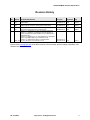
AM1808 SOM-M1 Hardware Specification
Hardware Documentation
Logic PD // Products
Published: April 2010
Last revised: May 2011
This document contains valuable proprietary and confidential information and the attached file contains source code, ideas, and
techniques that are owned by Logic PD, Inc. (collectively “Logic PD’s Proprietary Information”). Logic PD’s Proprietary Information
may not be used by or disclosed to any third party except under written license from Logic PD, Inc.
Logic PD, Inc. makes no representation or warranties of any nature or kind regarding Logic PD’s Proprietary Information or any
products offered by Logic PD, Inc. Logic PD’s Proprietary Information is disclosed herein pursuant and subject to the terms and
conditions of a duly executed license or agreement to purchase or lease equipment. The only warranties made by Logic PD, Inc., if
any, with respect to any products described in this document are set forth in such license or agreement. Logic PD, Inc. shall have no
liability of any kind, express or implied, arising out of the use of the Information in this document, including direct, indirect, special or
consequential damages.
Logic PD, Inc. may have patents, patent applications, trademarks, copyrights, trade secrets, or other intellectual property rights
pertaining to Logic PD’s Proprietary Information and products described in this document (collectively “Logic PD’s Intellectual
Property”). Except as expressly provided in any written license or agreement from Logic PD, Inc., this document and the information
contained therein does not create any license to Logic PD’s Intellectual Property.
The Information contained herein is subject to change without notice. Revisions may be issued regarding changes and/or additions.
© Copyright 2011, Logic PD, Inc. All Rights Reserved.
PN 1015746A
Logic PD, Inc. All Rights Reserved.
i
AM1808 SOM-M1 Hardware Specification
Revision History
REVISION DESCRIPTION
Schematic
PN & REV
APPROVAL DATE
Initial release
1015138 Rev A
1015640 Rev A
NJK
04/20/10
JCA
Added Appendix A and B containing mechanical drawings
1015138 Rev A
1015640 Rev A
JCA
09/23/10
3
JCA
-Section 2.4: Added Industrial temperature range; Added Caution
about system temperatures when enabling SATA;
1015138 Rev A
1015640 Rev A
JCA
11/05/10
A
-Section 1.5: Updated link for Logic PD hardware design files;
-Section 7.1: Updated J1.31 description since this signal is no
longer connected to the PMIC; Updated J1.39, 54 descriptions to
add resistor value;
-Section 7.2: Updated J2.91, 97, & 99 descriptions to add resistor
value; uP_EPWM0_TZ[0] is now connected to J2.99;
-Section 7.3: Added resistor value to J3.54 description;
SMC, JCA uP_SPI1_SCSn0 is now connected to J3.36
1015115 Rev C
1015774 Rev B
JCA
05/04/11
REV
1
2
EDITOR
JCA
Please check www.logicpd.com for the latest revision of this document, product change notifications, and
additional documentation.
PN 1015746A
Logic PD, Inc. All Rights Reserved.
ii
AM1808 SOM-M1 Hardware Specification
Table of Contents
1
2
3
4
5
Introduction ........................................................................................................................................... 1
1.1 Product Overview ............................................................................................................................. 1
1.2 Abbreviations, Acronyms, & Definitions ........................................................................................... 1
1.3 Nomenclature ................................................................................................................................... 2
1.4 Scope of Document.......................................................................................................................... 2
1.5 Additional Documentation Resources .............................................................................................. 2
Functional Specification ...................................................................................................................... 3
2.1 Processor ......................................................................................................................................... 3
2.1.1 AM1808 Processor .................................................................................................................... 3
2.1.2 AM1808 Processor Block Diagram ........................................................................................... 4
2.2 SOM Interface .................................................................................................................................. 4
2.2.1 AM1808 SOM-M1 Block Diagram ............................................................................................. 5
2.3 Mechanical Specifications ................................................................................................................ 5
2.3.1 Mechanical Characteristics of SOM .......................................................................................... 5
2.3.2 Interface Connectors ................................................................................................................. 6
2.4 Temperature Specifications ............................................................................................................. 6
Electrical Specification ........................................................................................................................ 7
3.1 Absolute Power Maximum Ratings .................................................................................................. 7
3.2 Recommended Power Operating Conditions................................................................................... 7
Peripheral Specification ....................................................................................................................... 8
4.1 Clocks............................................................................................................................................... 8
4.2 Memory ............................................................................................................................................ 8
4.2.1 Mobile DDR ............................................................................................................................... 8
4.2.2 SPI Flash ................................................................................................................................... 8
4.3 10/100 Ethernet PHY ....................................................................................................................... 8
4.4 Display Interface .............................................................................................................................. 9
4.5 Serial Interfaces ............................................................................................................................... 9
4.5.1 UART0-2 .................................................................................................................................... 9
4.5.2 SPI0/1 ........................................................................................................................................ 9
4.5.3 I2C0/1 ........................................................................................................................................ 9
4.5.4 McBSP0/1 ................................................................................................................................ 10
4.5.5 McASP0 ................................................................................................................................... 10
4.6 USB Interface ................................................................................................................................. 10
4.7 ADC/Touch Interface...................................................................................................................... 10
4.8 General Purpose I/O (GPIO) .......................................................................................................... 10
4.9 Expansion/Feature Options ........................................................................................................... 10
System Integration ............................................................................................................................. 12
5.1 Custom Configuration .................................................................................................................... 12
5.2 Resets ............................................................................................................................................ 12
5.2.1 Master Reset (MSTR_nRST)—Reset Input ............................................................................ 12
5.2.2 SOM Reset (RESETOUTn)—Reset output ............................................................................. 12
5.3 Interrupts ........................................................................................................................................ 13
5.4 JTAG Debugger Interface .............................................................................................................. 13
5.5 Power Management ....................................................................................................................... 13
5.5.1 System Power Supplies ........................................................................................................... 13
5.5.1.1 5V ...................................................................................................................................... 13
5.5.1.2 USB0_VBUS ..................................................................................................................... 13
5.5.1.3 MAIN_BATT_IN ................................................................................................................ 14
5.5.1.4 VRTC_IN ........................................................................................................................... 14
5.5.2 Dual Voltage I/O ...................................................................................................................... 14
5.5.3 System Power Management ................................................................................................... 14
5.5.4 Microprocessor ........................................................................................................................ 15
5.6 ESD Considerations ....................................................................................................................... 15
PN 1015746A
Logic PD, Inc. All Rights Reserved.
iii
AM1808 SOM-M1 Hardware Specification
6
7
Memory & I/O Mapping ....................................................................................................................... 16
Pin Descriptions & Functions ........................................................................................................... 17
7.1 J1 Connector 100-Pin Descriptions ............................................................................................... 17
7.2 J2 Connector 100-Pin Descriptions ............................................................................................... 23
7.3 J3 Connector 100-Pin Descriptions ............................................................................................... 27
Appendix A: SOM-M1 Mechanical Drawing ............................................................................................ 31
Appendix B: Example SOM-M1 Retention Methods .............................................................................. 33
PN 1015746A
Logic PD, Inc. All Rights Reserved.
iv
AM1808 SOM-M1 Hardware Specification
Table of Figures
Figure 2.1: AM1808 Processor Block Diagram ............................................................................................. 4
Figure 2.2: AM1808 SOM-M1 Block Diagram............................................................................................... 5
PN 1015746A
Logic PD, Inc. All Rights Reserved.
v
AM1808 SOM-M1 Hardware Specification
1
Introduction
1.1
Product Overview
The AM1808 System on Module (SOM) is a compact, product-ready hardware and software
solution that fast forwards embedded designs while reducing risk and controlling cost.
Based on Texas Instruments' AM1808 processor and designed in the SOM-M1 form factor, the
AM1808 module offers essential features for handheld and embedded networking applications.
The AM1808 SOM-M1 brings the industry leading low power ARM926 core to a small, off-theshelf solution. The standard SOM-M1 form factor allows developers to reuse existing baseboard
designs when upgrading to new Sitara processors, which extends roadmap possibilities for their
end-product.
Two Zoom™ Development Kit options allow developers to choose the platform best suited to their
application needs. By starting with the corresponding Zoom Development Kit, engineers can write
application software on the same hardware that will be used in their final product.
The compact size of the AM1808 SOM-M1 is ideal for medical patient monitoring wearables and
other portable instrumentation applications; the built-in Serial ATA (SATA) controller provides fast
access to large capacity storage devices. For medical, industrial, audio, and communication
products, the AM1808 SOM-M1 allows for powerful versatility, long-life, and greener products.
1.2
Abbreviations, Acronyms, & Definitions
ADC
BOM
BSP
BTB
DAC
DMA
EDMA
EMIFA
ESD
FIFO
HPI
GPIO
GPMC
Hi-Z
I2C
I2S
IC
I/O
IRQ
LCD
LDO
McASP
McBSP
mDDR
MDIO
MMU
MPU
OTG
PN 1015746A
Analog to Digital Converter
Bill of Materials
Board Support Package
Board-to-Board
Digital to Analog Converter
Direct Memory Access
Enhanced Direct Memory Access
External Memory Interface
Electrostatic Discharge
First In First Out
Host Port Interface
General Purpose Input Output
General Purpose Memory Controller
High Impedance
Inter-Integrated Circuit
Inter-Integrated Circuit Sound
Integrated Circuit
Input/Output
Interrupt Request
Liquid Crystal Display
Low Dropout (Regulator)
Multi-channel Audio Serial Port
Multi-channel Buffered Serial Port
Mobile Double Data Rate (RAM)
Management Data Input/Output
Memory Management Unit
Memory Protection Unit (ARM processor core)
On-the-Go (USB)
Logic PD, Inc. All Rights Reserved.
1
AM1808 SOM-M1 Hardware Specification
PCB
PCMCIA
PHY
PLL
PWM
RTC
SATA
SDRAM
SOM
SOM-M1
SPI
STN
TFT
TI
TSC
UART
uPP
USB
VLIW
VPIF
1.3
Printed Circuit Board
Personal Computer Memory Card International Association (PC Cards)
Physical Layer
Phase Lock Loop
Pulse Width Modulation
Real Time Clock
Serial ATA
Synchronous Dynamic Random Access Memory
System on Module
SOM form factor type used for the AM1808 modules
Standard Programming Interface
Super-Twisted Nematic (LCD)
Thin Film Transistor (LCD)
Texas Instruments
Touch Screen Controller
Universal Asynchronous Receive Transmit
Universal Parallel Port
Universal Serial Bus
Very Long Instruction Word
Video Port Interface
Nomenclature
The terms “SOM” and “SOM-M1” are used interchangeably throughout this document and can be
assumed to mean the same thing within this text. The SOM-M1 is a specific form factor type of
Logic PD’s SOM.
1.4
Scope of Document
This Hardware Specification is unique to the design and use of the AM1808 SOM-M1 as
designed by Logic PD and does not intend to include information outside of that scope. Detailed
information about the Texas Instruments (TI) AM1808 processor or any other device component
on the SOM can be found in their respective manuals and specification documents; please see
Section 1.5 for additional resources.
1.5
Additional Documentation Resources
The following documents or documentation resources are referenced within this Hardware
Specification.
■
TI’s AM1808 ARM Microprocessor Datasheet, User Guides, Application Notes, White Papers,
and Errata
http://www.ti.com/am1808
■
TI’s TPS65070 Datasheet
http://focus.ti.com/docs/prod/folders/print/tps65070.html
■
USB 2.0 Specification, available from USB.org
http://www.usb.org/developers/docs/
■
U-Boot documentation
http://www.denx.de/wiki/U-Boot/WebHome
■
Logic PD AM1808 Hardware Design Files (BOM, Schematic, and Layout) for all boards
included in the development kits, as well as all standard configurations SOMs. Sign into your
account on Logic PD’s website to access the files for your specific development kit and SOM.
http://support.logicpd.com/auth/
PN 1015746A
Logic PD, Inc. All Rights Reserved.
2
AM1808 SOM-M1 Hardware Specification
2
Functional Specification
2.1
Processor
2.1.1
AM1808 Processor
The AM1808 SOM-M1 uses TI’s high-performance AM1808 microprocessor. This device contains
an ARM926EJ-S MPU core and provides many integrated on-chip peripherals, including:
■
■
■
■
■
■
■
■
■
■
ARM® ARM926EJ-S™ RISC core
Integrated LCD Controller
□ Up to 1024 x 1024 x 16 bit color
Three UARTs
I2S codec interface
Universal Serial Bus (USB)
□ One high-speed USB 2.0 On-the-Go (OTG) interface
□ One full-speed USB 1.1 host interface
Serial ATA Controller
□ SATA I (1.5Gb/s) or SATA II (3Gb/s)
Many general purpose I/O (GPIO) signals
Programmable timers
Real time clock (RTC)
Low power modes
IMPORTANT NOTE: The AM1808 processor pinout is heavily multiplexed; using one peripheral
may preclude the use of another. Users should carefully review the processor pinout, SOM
pinout, and AM1808 multiplexing table. See TI’s AM1808 ARM Microprocessor Datasheet, User
Guides, and Application Notes for additional information.
IMPORTANT NOTE: Please visit TI’s website for errata on the AM1808;
http://www.ti.com/am1808.
PN 1015746A
Logic PD, Inc. All Rights Reserved.
3
AM1808 SOM-M1 Hardware Specification
2.1.2
AM1808 Processor Block Diagram
Figure 2.1: AM1808 Processor Block Diagram
Note: The block diagram pictured above comes from TI’s AM1808 ARM Microprocessor Data
Sheet (document number SPRS653–February 2010). Available from TI’s website:
http://www.ti.com/am1808.
2.2
SOM Interface
Logic PD’s common SOM interface allows for easy migration to new processors and technology.
Logic PD is constantly researching and developing new technologies to improve performance,
lower cost, and increase feature capabilities. By using the common SOM footprint, it is possible to
take advantage of Logic PD’s work without having to re-spin the old design in certain cases
dependent upon peripheral usage. Contact Logic PD sales for more information
([email protected]).
In fact, encapsulating a significant amount of your design onto the SOM reduces any long-term
risk of obsolescence. If a component on the SOM design becomes obsolete, Logic PD will simply
design for an alternative part that is transparent to your product. Furthermore, Logic PD tests all
SOMs prior to delivery, decreasing time-to-market and ensuring a simpler and less costly
manufacturing process.
PN 1015746A
Logic PD, Inc. All Rights Reserved.
4
AM1808 SOM-M1 Hardware Specification
2.2.1
AM1808 SOM-M1 Block Diagram
Figure 2.2: AM1808 SOM-M1 Block Diagram
2.3
Mechanical Specifications
2.3.1
Mechanical Characteristics of SOM
Parameter
Min
Typical
Max
Unit
Notes
Dimensions
—
30 x 40 x 4.1
—
mm
1
Weight
—
7
—
Grams
2
Connector Insertion/Removal
—
30
—
Cycles
—
Notes:
1. The AM1808 SOM-M1 in the Zoom AM1808 EVM Development Kit includes power
measurement circuitry along one edge of the SOM. This additional circuitry increases the
PCB size to 33.7 x 40 x 4.1 mm. All other AM1808 SOM-M1 modules, including those
available in production volumes, are the typical size listed above.
2. May vary depending on SOM configuration.
PN 1015746A
Logic PD, Inc. All Rights Reserved.
5
AM1808 SOM-M1 Hardware Specification
2.3.2
Interface Connectors
The AM1808 SOM-M1 connects to a PCB baseboard through three 100-pin board-to-board (BTB)
socket connectors.
2.4
Ref Designator
Manufacturer
SOM Connector P/N
Mating Connector P/N
J1, J2, J3
Hirose
DF40C-100DP-0.4V(51)
DF40C-100DS-0.4V(51)
Temperature Specifications
Parameter
Min
Typical
Max
Unit
Notes
0
25
70
°C
—
Industrial Operating Temperature
-40
25
85
°C
—
Storage Temperature
-40
25
85
°C
—
Commercial Operating Temperature
CAUTION: Systems using the SATA interface on the AM1808 SOM-M1 may require additional
heat dissipation techniques in order to comply with the high end of the system temperature
limitation. It is the responsibility of the engineer to ensure the AM1808 SOM-M1 maintains a safe
operating temperature within the system.
PN 1015746A
Logic PD, Inc. All Rights Reserved.
6
AM1808 SOM-M1 Hardware Specification
3
Electrical Specification
3.1
Absolute Power Maximum Ratings
Parameter
Symbol
Rating
Unit
DC 5 V Supply Voltage
5V
0.0 to 7.0
V
DC Main Battery Input Voltage
MAIN_BATT_IN
0.0 to 7.0
V
RTC Backup Battery Voltage
BACKUP_BATT
0.0 to 7.0
V
NOTE: These stress ratings are only for transient conditions. Operation at, or beyond, absolute
maximum rating conditions may affect reliability and cause permanent damage to the SOM and
its components.
3.2
Recommended Power Operating Conditions
Parameter
Min
Typical
Max
DC Main Battery Input Voltage
3.3
3.6
4.2
DC 5V Voltage
3.6
5.0
DC 5V Active Current
—
250
DC 5V Active Current, no SATA
—
DC RTC Backup Battery Voltage
1.8
Unit Notes
V
4
5.8
V
3
—
mA
5
151
—
mA
6
3.3
3.6
V
VREF
V
2
0.65*VREF (1.8V)
Input Signal High Voltage
2 (3.3V)
—
Input Signal Low Voltage
GND
—
0.8 (3.3V)
V
2
VREF
V
2
V
2
0.35*VREF (1.8V)
2.40 (3.3V)
Output Signal High Voltage
VREF-0.45 (1.8V)
—
Output Signal Low Voltage
GND
—
0.40 (3.3V)
0.45 (1.8V)
Notes:
1. General note: CPU power rails are sequenced on the module.
2. VREF represents the peripheral I/O supply reference for the specific CPU voltage rail. For
VI/OH and VI/OL, different values are provided for VREF = 1.8V and 3.3V.
3. Please see Section 5.5.1.1 for detailed information about 5V usage on the AM1808 SOM-M1.
4. Please see Section 5.5.1.3 for detailed information about MAIN_BATT_IN usage on the
AM1808 SOM-M1.
5. Measurement was taken with a system consisting of SOM and baseboard. The SOM was
running the standard U-Boot software image, version 2009.11. This power measurement
represents current consumption on the SOM only (baseboard and UI board were excluded).
6. Same setup as Note 5 with the exception that the SATA clock generator was disabled by
populating R146.
PN 1015746A
Logic PD, Inc. All Rights Reserved.
7
AM1808 SOM-M1 Hardware Specification
4
Peripheral Specification
4.1
Clocks
The AM1808 SOM-M1 contains two crystals. One crystal is used to generate clocks for the
processor core(s) and peripherals. The second crystal is dedicated to the RTC module.
The AM1808 processor includes on-chip Phase Locked Loops (PLLs) and signal dividers which
generate all core/peripheral clocks from a single external 24.000 MHz crystal. The maximum core
processor operating frequency is 450 MHz. Optionally, on-chip module PLL0 provides an output:
SOM Pin#
SOM Net Name
AM1808 Processor Pin
J3.18
uP_OBSCLK
CLKOUT/ UHPI_HDS2/ GP6[14]
IMPORTANT NOTE: Please see TI’s AM1808 ARM Microprocessor Datasheet and User Guides
for additional information about processor clocking.
The AM1808 processor also contains an on-chip Real Time Clock (RTC) module which is driven
by an external 32.768 kHz crystal. The highly configurable RTC module provides a time reference
to applications running on the AM1808. The SOM contains a dedicated power input pin (J2.64,
“VRTC_IN”) and low dropout (LDO) which supplies the processor’s dedicated RTC power rail
(RTC_CVDD)
IMPORTANT NOTE: For more information on RTC power, see Section 5.5.1.4. For more
information about software configuration of the RTC, see TI’s AM1808 ARM Microprocessor
Datasheet and User Guides.
4.2
Memory
4.2.1
Mobile DDR
The AM1808 SOM-M1 provides volatile memory via a single mDDR chip. Please refer to the
AM1808 SOM-M1 Bill of Materials (BOM) for the memory density of your specific SOM.
Other memory densities may be available for SOMs in production volumes. Please contact Logic
PD Sales about custom configurations if your design requires different memory densities from
Logic PD’s standard SOM configurations: [email protected].
4.2.2
SPI Flash
The AM1808 SOM-M1 provides non-volatile memory via an 8 MB SPI flash chip. This is also the
default boot device.
Other memory densities may be available for SOMs in production volumes. Please contact Logic
PD Sales about custom configurations if your design requires different memory densities from
Logic PD’s standard SOM configurations: [email protected].
4.3
10/100 Ethernet PHY
The AM1808 SOM-M1 uses an SMSC LAN8710 Ethernet PHY to provide an easy-to-use
networking interface. The four analog PHY interface signals (transmit/receive) each require an
external impedance matching circuit to operate properly. Logic PD provides an example circuit
PN 1015746A
Logic PD, Inc. All Rights Reserved.
8
AM1808 SOM-M1 Hardware Specification
schematic in the AM1808 Baseboard Schematics. Please note the TX+/- and RX+/- pairs must be
routed as differential pairs on the baseboard PCB.
4.4
Display Interface
The AM1808 has a built-in LCD controller supporting both synchronous (raster-type) and
asynchronous (memory-mapped) panels.
The synchronous (raster) module supports STN, color STN, and TFT panels at a resolution of up
to 1024 x 1024 x 16-bit color.
The asynchronous (memory-mapped) module supports a broad range of displays from
monochrome character displays to TFT smart LCD panels. Displays driven by this module must
contain their own memory and timing circuitry.
The signals from the AM1808 LCD controller can be interfaced through the expansion
connectors. See TI’s AM1808 ARM Microprocessor Datasheet for further information on the
integrated LCD controller.
IMPORTANT NOTE: Using the internal graphics controller will affect processor performance.
Selecting display resolutions and color bits per pixel will vary processor busload.
4.5
Serial Interfaces
The AM1808 SOM-M1 comes with the following serial channels: UART0-2, SPI0/1, I2C0/1,
McBSP0/1, and McASP. If additional serial channels are required, please contact Logic PD for
reference designs. Please see TI’s AM1808 User Guides for further information regarding serial
communications.
4.5.1
UART0-2
The AM1808 SOM-M1 provides three UART ports. UART0, UART1, and UART2 are
asynchronous 16C550-compatible UARTs. These UARTs are high-speed serial interfaces that
use 16-byte TX and RX FIFO registers; they are capable of sending and receiving serial data
simultaneously. The signals from the SOM are not RS232 level signals. The end-product design
must provide an external transceiver for RS232 applications. Logic PD has provided an example
reference design with the Zoom AM1808 Development Kits. When choosing an RS232
transceiver, the designer should keep in mind cost, availability, ESD protection, and data rates.
UART2 has been configured as the main SOM serial port. The UART2 baud rate is set to a
default 115.2 Kbits/sec, though it supports most common serial baud rates.
4.5.2
SPI0/1
The AM1808 SOM-M1 provides two SPI ports with multiple chip selects.
SPI1 is the default boot source for the AM1808 SOM-M1. A serial flash chip is attached to SPI1
CS0.
4.5.3
I2C0/1
The AM1808 SOM-M1 provides two I2C ports. The clock and data signals for both ports have
4.7K pull-up resistors to their respective power rails on the SOM. Please see TI’s AM1808 User
Guides for further information.
PN 1015746A
Logic PD, Inc. All Rights Reserved.
9
AM1808 SOM-M1 Hardware Specification
I2C0 has been configured as the main SOM I2C port. I2C0 is used to control/configure many ICs
on the SOM as well as the Zoom AM1808 Development Kits.
4.5.4
McBSP0/1
The AM1808 SOM-M1 supports two Multi-channel Buffered Serial Port (McBSP) interfaces.
These interfaces are primarily designed to support AC97 and IIS modes, but they can also be
configured for other serial formats. However, the McBSPs are not intended to be used as highspeed interfaces.
4.5.5
McASP0
The AM1808 SOM-M1 supports one Multi-channel Audio Serial Port (McASP). The McASP
interface supports TDM streams, I2S protocols, and DIT.
Logic PD has provided an example reference design with the Zoom AM1808 Development Kits;
this reference design interfaces the AM1808 McASP to a TLV320AIC3106 audio codec.
4.6
USB Interface
The AM1808 SOM-M1 supports one USB 1.1 full-speed host port and one USB 2.0 OTG port,
which can function as a host or device/client. The USB 2.0 port can operate at up to 480 Mbit/sec,
and the USB 1.1 port can operate at up to 12 Mbit/sec. Both the USB 1.1 and USB 2.0 controllers
are internal to the AM1808 processor. For more information on using both the USB host and OTG
interfaces, please see TI’s AM1808 User Guides.
IMPORTANT NOTE: In order to correctly implement USB on the SOM, additional impedance
matching circuitry may be required on the USBx_D+ and USBx_D- signals before they can be
used. USB 2.0 requirements specify the signals must be routed as differential pairs with a 90 ohm
differential impedance. Refer to the USB 2.0 Specification for detailed information.
4.7
ADC/Touch Interface
The touch screen controller (TSC) on the AM1808 SOM-M1 is an integrated feature of the
TPS65070 PMIC. This TSC is used to support standard 4-wire resistive touch panels. The
TPS65070 is connected to the AM1808 by the I2C0 interface. Please see TI’s TPS65070
Datasheet for more information.
4.8
General Purpose I/O (GPIO)
Logic PD designed the AM1808 SOM-M1 to be flexible and provide multiple options for analog
and digital GPIO. There are numerous digital GPIO pins on the SOM that interface to the
AM1808. See Section 7 of this document for more information. If certain peripherals are not
desired, such as the LCD controller, chip selects, IRQs, or UARTs, then more GPIO pins become
available.
4.9
Expansion/Feature Options
The AM1808 SOM-M1 was designed for expansion and a variable feature set, providing all the
necessary control signals and bus signals to expand the user’s design. Some of these signals are
buffered before reaching the expansion connectors. See TI’s AM1808 ARM Microprocessor
Datasheet and User Guides and Logic PD’s AM1808 SOM-M1 Schematics for more details. Logic
PD has experience implementing additional options, including: audio codecs, Ethernet ICs,
PN 1015746A
Logic PD, Inc. All Rights Reserved.
10
AM1808 SOM-M1 Hardware Specification
co-processors, and components on SOMs. Please contact Logic PD for potential reference
designs before selecting your peripherals.
PN 1015746A
Logic PD, Inc. All Rights Reserved.
11
AM1808 SOM-M1 Hardware Specification
5
System Integration
5.1
Custom Configuration
The AM1808 SOM-M1 was designed to meet multiple applications for users with specific design
and budget requirements. As a result, this SOM supports a variety of embedded operating
systems, flexible mDDR and SPI flash memory footprints, and other hardware configurations. If
your application needs require unique hardware or software configurations, please contact Logic
PD Sales about custom SOMs available in production volumes: [email protected].
5.2
Resets
The AM1808 SOM-M1 has a reset input (MSTR_nRST) and a reset output (RESETOUTn).
External devices use MSTR_nRST to assert reset to the product. The AM1808 SOM-M1 uses
RESETOUTn to indicate to other devices that the SOM is in reset.
5.2.1
Master Reset (MSTR_nRST)—Reset Input
Logic PD suggests that custom designs implementing the AM1808 SOM-M1 use the
MSTR_nRST signal as the “pin-hole” reset used in commercial embedded systems. The
MSTR_nRST triggers a power-on-reset event to the AM1808 processor and resets the entire
CPU.
IMPORTANT NOTE: Any custom reset circuit design should guard the assertion of the reset lines
during a low power state so as to prevent power-up in a low or bad power condition. (Powering up
in a low or bad power condition will cause data corruption and, possibly, temporary system
lockup). See the “Power Management” section of this document for further details. A low pulse on
the MSTR_nRST signal will cause a system-wide reset.
Low Pulse on MSTR_nRST Signal:
A low pulse on the MSTR_nRST signal, asserted by an external source (for example, the reset
button on the custom design application) will bring MSTR_nRST low until the assertion source is
de-asserted. There is no delay beyond the de-assertion of the external MSTR_nRST signal
source, so the custom design must ensure that the assertion time is sufficient for all related
peripherals.
Logic PD suggests that for any external assertion source that triggers the MSTR_nRST signal,
analog or digital, de-bouncing should be used to generate a clean, one-shot reset signal.
5.2.2
SOM Reset (RESETOUTn)—Reset output
All hardware peripherals should connect their hardware-reset pin to the RESETOUTn signal on
the expansion connector. Internally, all AM1808 SOM-M1 peripheral hardware reset pins are
connected to the RESET_nOUT net.
If the output of the onboard voltage-monitoring circuit is asserted (active low), the user can expect
to lose information stored in RAM. The data loss occurs because the CPU is reset to its reset
defaults.
PN 1015746A
Logic PD, Inc. All Rights Reserved.
12
AM1808 SOM-M1 Hardware Specification
5.3
Interrupts
The AM1808 interrupt controller allows the ARM core to enable, disable, trigger, or service all
interrupts. Most external GPIO signals can also be configured as interrupt inputs by configuring
their pin control registers. Logic PD BSPs setup and process all onboard system and external
SOM interrupt sources. Refer to TI’s AM1808 ARM Microprocessor Datasheet and User Guides
for further information on using interrupts.
5.4
JTAG Debugger Interface
The JTAG connection on the AM1808 allows recovery of corrupted flash memory, real-time
application debug, and ARM core development. There are several third-party JTAG debuggers
available for TI microprocessors. The following signals make up the JTAG interface to the
AM1808 processor: TDI, TMS, TCK, TDO, nTRST, RTCK, EMU0, EMU1, and MSTR_nRST
(MSTR_nRST is only required for some JTAG tools; see the JTAG tool documentation for exact
pinout). These signals should interface directly to a 14 or 20-pin 0.1” through-hole connector, as
shown on Logic PD’s AM1808 Baseboard Schematic.
IMPORTANT NOTE: When laying out the JTAG connector, realize that it may not be numbered
as a standard 14 or 20-pin 0.1” insulation displacement connector (IDC) through-hole connector.
See the AM1808 Baseboard Schematic for further details. Each JTAG tool vendor may define the
IDC connector pin-out differently.
5.5
Power Management
5.5.1
System Power Supplies
In order to ensure a flexible design, the AM1808 SOM-M1 has the following power areas:
MAIN_BATT_IN, 5V, RTC_BATT. All power areas are inputs to the SOM. The module also
provides output reference voltage 3.3V_or_1.8V. 3.3V_or_1.8V is an output from the SOM, and
should only be used as a reference voltage input to level shifting devices on baseboard designs.
IMPORTANT NOTE: If USB0_VBUS is powered externally it will power the SOM, even if
MAIN_BATT_IN and 5V are disconnected. Additionally, USB0_VBUS can charge
MAIN_BATT_IN. Please refer to the TPS65070 Datasheet for more information.
5.5.1.1
5V
The 5V input is the main source of power for the AM1808 SOM-M1. If power is present at the 5V
input, the TPS65070 PMIC will preferentially select this power source over all other sources. If
appropriate voltage is applied to the 5V input, the TPS65070 PMIC and AM1808 processor will
immediately start up and run. 5V input is capable of charging MAIN_BATT_IN.
For startup, acceptable 5V input range is: 3.6V < 5V input < 5.8V
At runtime, 5V range is: UVLO < 5V input < 5.8V
UVLO = UnderVoltage LockOut
UVLO = 3.0V (default), 2.8V < UVLO < 3.25V (programmable)
5.5.1.2
USB0_VBUS
USB0_VBUS is an optional power source for the AM1808 SOM-M1. If power is present at the
USB0_VBUS input, the TPS65070 PMIC will preferentially select this source over
PN 1015746A
Logic PD, Inc. All Rights Reserved.
13
AM1808 SOM-M1 Hardware Specification
MAIN_BATT_IN. If appropriate voltage is applied to the USB0_VBUS input, the TPS65070 PMIC
and AM1808 processor will immediately start up and run. The USB0_VBUS input is capable of
charging MAIN_BATT_IN.
5.5.1.3
MAIN_BATT_IN
The MAIN_BATT_IN input is designed to be connected to a typical single lithium-ion battery. The
TPS65070 PMIC will only power the SOM from MAIN_BATT_IN if power is not present at 5V or
USB0_VBUS inputs. If appropriate voltage is applied to the MAIN_BATT_IN input, the TPS65070
PMIC and AM1808 processor will NOT immediately start up and run; a momentary low signal is
also required on the PMIC_PB_IN pin. The TPS65070 PMIC is capable of charging
MAIN_BATT_IN from either the 5V input or the USB0_VBUS input.
For startup, MAIN_BATT_IN range is: 3.6V < MAIN_BATT_IN < 4.2V
At runtime, MAIN_BATT_IN range is: UVLO < MAIN_BATT_IN < 4.2V
UVLO = UnderVoltage LockOut
UVLO = 3.0V (default), 2.8V < UVLO < 3.25V (programmable)
IMPORTANT NOTES:
Though UVLO may be set as low as 2.8V, not all AM1808 SOM-M1 circuits are capable of 2.8V
operation. The SOM contains an internal 3.3V power rail, and devices connected to this rail may
have dropout voltages much greater than UVLO. See Section 3.2 for the recommended range of
input voltages.
Before designing a system which powers the AM1808 SOM-M1 from MAIN_BATT_IN, the user
should first review the following documents: TPS65070 Datasheet, AM1808 SOM-M1 Schematic,
and AM1808 Baseboard Schematic.
5.5.1.4
VRTC_IN
The VRTC_IN power rail is used to power the onboard RTC module. Always power this rail to
maintain the clock of the product. A lithium-ion coin cell typically supplies power to this rail.
5.5.2
Dual Voltage I/O
The AM1808 processor and AM1808 SOM-M1 uniquely support dual-voltage I/O. The user may
select an operating voltage of either 1.8V or 3.3V through “IO_VOLTAGE_SEL” J1.37. For 3.3V
operation, J1.37 should be left unconnected. For 1.8V operation, J1.37 should be tied directly to
GND.
5.5.3
System Power Management
Good power management design is important in any system development and embedded system
design is no exception. In embedded system design, power management is typically one of the
most complicated areas due to the dramatic effect it has on product cost, performance, usability,
and overall customer satisfaction. Many factors affect a power-efficient hardware design: power
supply selection (efficiency), clocking design, IC and component selection, etc. The AM1808
SOM-M1 was designed with these aspects in mind while also providing maximum flexibility in
software and system integration.
On the AM1808 there are many different software configurations that drastically affect power
consumption: microprocessor core clock frequency, bus clock frequency, peripheral clocks, bus
PN 1015746A
Logic PD, Inc. All Rights Reserved.
14
AM1808 SOM-M1 Hardware Specification
modes, power management states; peripheral power states and modes; product user scenarios;
interrupt handling; and display settings (resolution, backlight, refresh, bits per pixel, etc). These
settings are typically initialized in the startup software routines and may be modified later in the
operating system and application software. Information for these items can be found in the
appropriate documents such as the U-Boot User’s Manual, TI’s AM1808 ARM Microprocessor
Datasheet and User Guides, TPS65070 Datasheet, and Logic PD’s AM1808 SOM-M1
Schematic.
5.5.4
Microprocessor
The AM1808 processor’s power management scheme was designed for ultra-low power, so
naturally the static and dynamic power consumption has very flexible controls allowing designers
to configure the processor to minimize end-product power consumption. Most peripheral modules
can be powered on/off individually, and the core(s) can enter various levels of standby/sleep. To
implement a low-power system, users should review TI’s AM1808 ARM Microprocessor
Datasheet and User Guides, TPS65070 Datasheet, and Logic PD’s AM1808 SOM-M1
Schematic.
5.6
ESD Considerations
The AM1808 SOM-M1 was designed to interface to a customer’s peripheral board, while
remaining low cost and adaptable to many different applications. The SOM does not provide any
onboard ESD protection circuitry—this must be provided by the product it is used in. Logic PD
has extensive experience in designing products with ESD requirements. Please contact Logic PD
if you need any assistance in ESD design considerations.
PN 1015746A
Logic PD, Inc. All Rights Reserved.
15
AM1808 SOM-M1 Hardware Specification
6
Memory & I/O Mapping
AM1808 chip select signals are described listed below:
Chip Select
Device/Feature
Notes
SPI0_SCS[0:5] Not Available
MDIO/MII comm. interfaces on SOM
SPI1_SCS[0]
LCD Backlight PWM on dev kit
SPI Flash (boot)
SPI1_SCS[1]
LCD Backlight Power on dev kit
SPI1_SCS[2:3]
Available for use by an off-board external device
SPI1_SCS[4]
UART TXD on dev kit
SPI1_SCS[5]
UART RXD on dev kit
SPI1_SCS[6]
Not Available
I2C0 is used extensively for configuration/control
on both the SOM and dev. kit
SPI1_SCS[7]
Not Available
I2C0 is used extensively for configuration/control
on both the SOM and dev. kit
EMA_CS[0]
Available for use by an off-board external device
EMA_CS[2:5]
Available for use by an off-board external device
UHPI_HCS
Available for use by an off-board external device
PN 1015746A
Logic PD, Inc. All Rights Reserved.
16
AM1808 SOM-M1 Hardware Specification
7
Pin Descriptions & Functions
SOM Net Name: This is the name used in Logic PD’s AM1808 SOM-M1 Schematics.
Processor Name: This is the name used TI’s AM1808 ARM Microprocessor Datasheet.
I/O: This indicates the default pin configuration after booting U-Boot. Most pins can be
reconfigured as either input or output. Consult Logic PD’s AM1808 SOM-M1 Schematics and TI’s
AM1808 ARM Microprocessor Datasheet for more information.
Description: If a pull-up or pull-down resistor is present on the AM1808 SOM-M1, it will be noted
here. Special usage tips and cautions will be noted here. Consult Logic PD’s AM1808 SOM-M1
Schematics and TI’s AM1808 ARM Microprocessor Datasheet for more information.
7.1
J1 Connector 100-Pin Descriptions
J1 Pin# SOM Net Name
Processor Name
I/O Voltage
1
uP_VPIF_DOUT8
VP_DOUT[8]/
LCD_D[8]/
UPP_XD[0]/
GP7[0]/ BOOT[0]
LCD G3 data bit when outputting RGB565
data to an RGB666 display.
4.7k pull-down on SOM.
3.3V or 1.8V Used to latch boot mode at startup (see
Hi-Z (see Note 1) Note 2).
uP_VPIF_DOUT0
VP_DOUT[0]/
LCD_D[0]/
UPP_XD[8]/
GP7[8]
3.3V or 1.8V LCD B1 data bit when outputting RGB565
Hi-Z (see Note 1) data to an RGB666 display.
uP_VPIF_DOUT9
VP_DOUT[9]/
LCD_D[9]/
UPP_XD[1]/
GP7[1]/ BOOT[1]
LCD_G4 data bit when outputting RGB565
data to an RGB666 display.
4.7k pull-down on SOM.
3.3V or 1.8V Used to latch boot mode at startup (see
Hi-Z (see Note 1) Note 2).
uP_VPIF_DOUT1
VP_DOUT[1]/
LCD_D[1]/
UPP_XD[9]/
GP7[9]
3.3V or 1.8V LCD_B2 data bit when outputting RGB565
Hi-Z (see Note 1) data to an RGB666 display.
uP_VPIF_DOUT10
VP_DOUT[10]/
LCD_D[10]/
UPP_XD[2]/
GP7[2]/ BOOT[2]
LCD_G5 data bit when outputting RGB565
data to an RGB666 display.
4.7k pull-up on SOM.
3.3V or 1.8V Used to latch boot mode at startup (see
Hi-Z (see Note 1) Note 2).
uP_VPIF_DOUT2
VP_DOUT[2]/
LCD_D[2]/
UPP_XD[10]/
GP7[10]
3.3V or 1.8V LCD_B3 data bit when outputting RGB565
Hi-Z (see Note 1) data to an RGB666 display.
uP_VPIF_DOUT11
VP_DOUT[11]/
LCD_D[11]/
UPP_XD[3]/
GP7[3]/ BOOT[3]
LCD_R1 data bit when outputting RGB565
data to an RGB666 display.
4.7k pull-up on SOM.
3.3V or 1.8V Used to latch boot mode at startup (see
Hi-Z (see Note 1) Note 2).
uP_VPIF_DOUT3
VP_DOUT[3]/
LCD_D[3]/
UPP_XD[11]/
GP7[11]
3.3V or 1.8V LCD_B4 data bit when outputting RGB565
Hi-Z (see Note 1) data to an RGB666 display.
2
3
4
5
6
7
8
PN 1015746A
Description
Logic PD, Inc. All Rights Reserved.
17
AM1808 SOM-M1 Hardware Specification
J1 Pin# SOM Net Name
Processor Name
I/O Voltage
9
uP_VPIF_DOUT12
VP_DOUT[12]/
LCD_D[12]/
UPP_XD[4]/
GP7[4]/ BOOT[4]
LCD_R2 data bit when outputting RGB565
data to an RGB666 display.
4.7k pull-down on SOM.
3.3V or 1.8V Used to latch boot mode at startup (see
Hi-Z (see Note 1) Note 2).
uP_VPIF_DOUT4
VP_DOUT[4]/
LCD_D[4]/
UPP_XD[12]/
GP7[12]
LCD_B5 data bit when outputting RGB565
data to an RGB666 display. Notice that
LCD_B0 is omitted; LCD_B5 (Blue MSB) is
3.3V or 1.8V also connected to LCD_B0 (Blue LSB)
Hi-Z (see Note 1) when driving an 18 bit display with 16 bits.
uP_VPIF_DOUT13
VP_DOUT[13]/
LCD_D[13]/
UPP_XD[5]/
GP7[5]/ BOOT[5]
LCD_R3 data bit when outputting RGB565
data to an RGB666 display.
4.7k pull-down on SOM.
3.3V or 1.8V Used to latch boot mode at startup (see
Hi-Z (see Note 1) Note 2).
uP_VPIF_DOUT5
VP_DOUT[5]/
LCD_D[5]/
UPP_XD[13]/
GP7[13]
3.3V or 1.8V LCD_G0 data bit when outputting RGB565
Hi-Z (see Note 1) data to an RGB666 display.
uP_VPIF_DOUT14
VP_DOUT[14]/
LCD_D[14]/
UPP_XD[6]/
GP7[6]/ BOOT[6]
LCD_R4 data bit when outputting RGB565
data to an RGB666 display.
4.7k pull-down on SOM.
3.3V or 1.8V Used to latch boot mode at startup (see
Hi-Z (see Note 1) Note 2).
uP_VPIF_DOUT6
VP_DOUT[6]/
LCD_D[6]/
UPP_XD[14]/
GP7[14]
3.3V or 1.8V LCD_G1 data bit when outputting RGB565
Hi-Z (see Note 1) data to an RGB666 display.
uP_VPIF_DOUT15
VP_DOUT[15]/
LCD_D[15]/
UPP_XD[7]/
GP7[7]/ BOOT[7]
LCD_R5 data bit when outputting RGB565
data to an RGB666 display. Notice that
LCD_R0 is omitted; LCD_R5 (Red MSB) is
also connected to LCD_R0 (Red LSB)
when driving an 18 bit display with 16 bits.
4.7k pull-down on SOM.
3.3V or 1.8V Used to latch boot mode at startup (see
Hi-Z (see Note 1) Note 2).
uP_VPIF_DOUT7
VP_DOUT[7]/
LCD_D[7]/
UPP_XD[15]/
GP7[15]
3.3V or 1.8V LCD_G2 data bit when outputting RGB565
Hi-Z (see Note 1) data to an RGB666 display.
uP_LCD_HSYNC
MMCSD1_DAT[5]/
3.3V or 1.8V
LCD_HSYNC/
GP8[9]
Hi-Z (see Note 1) —
18
uP_LCD_PCLK
MMCSD1_DAT[7]/
LCD_PCLK/
3.3V or 1.8V
GP8[11]
Hi-Z (see Note 1) 22 ohm series R on SOM.
19
DGND
—
I
GND
Ground. Connect to digital ground.
20
DGND
—
I
GND
Ground. Connect to digital ground.
uP_LCD_VSYNC
MMCSD1_DAT[4]/
LCD_VSYNC/
3.3V or 1.8V
GP8[8]
Hi-Z (see Note 1) —
22
uP_LCD_MCLK
MMCSD1_DAT[6]/
3.3V or 1.8V
LCD_MCLK/
GP8[10]
Hi-Z (see Note 1) 22 ohm series R on SOM.
23
uP_LCD_AC_ENB_C LCD_AC_ENB_C
Sn
S/ GP6[0]
10
11
12
13
14
15
16
17
21
PN 1015746A
Description
3.3V or 1.8V
Hi-Z (see Note 1) —
Logic PD, Inc. All Rights Reserved.
18
AM1808 SOM-M1 Hardware Specification
J1 Pin# SOM Net Name
Processor Name
I/O Voltage
24
uP_VPIF_CLKIN0
VP_CLKIN0/
UHPI_HCS/
GP6[7]/
UPP_2xTXCLK
3.3V or 1.8V
Hi-Z (see Note 1) —
25
uP_USB0_DRVVBUS USB0_DRVVBUS
O
—
Description
—
26
uP_VPIF_DIN14
VP_DIN[14]_
HSYNC/
UHPI_HD[6]/
UPP_CHA_D[6]
27
uP_VPIF_CLKO3
VP_CLKOUT3/
GP6[1]
3.3V or 1.8V
Hi-Z (see Note 1) 22 ohm series R on SOM.
uP_VPIF_DIN15
VP_DIN[15]_
VSYNC/
UHPI_HD[7]/
UPP_CHA_D[7]
3.3V or 1.8V
Hi-Z (see Note 1) —
28
29
uP_RESETn
RESET
30
RFU
—
31
uP_NMIn
RSVDN
uP_VPIF_DIN13
VP_DIN[13]_
FIELD/
UHPI_HD[5]/
UPP_CHA_D[5]
32
33
3.3V or 1.8V
Hi-Z (see Note 1) —
I
4.7k pull-up on SOM.
3.3V or 1.8V Also connected to PGOOD on TPS65070
(see Note 4) PMIC. PGOOD is an open drain output.
NA NA
I
Reserved for future use. Do not connect.
3.3V or 1.8V Reserved. 4.7k pull-up on SOM.
(see Note 1)
3.3V or 1.8V
Hi-Z (see Note 1) —
Input to TPS65070 PMIC, not AM1808.
See Section 5.5.1.3.
Buffered version of this input can be read
on AM1808 pin EMA_RAS / GPIO2[5]
PMIC_PB_IN
—
I/O —
34
uP_VPIF_DIN12
VP_DIN[12]/
UHPI_HD[4]/
UPP_CHA_D[4]
3.3V or 1.8V
Hi-Z (see Note 1) —
35
RFU
—
NA NA
36
uP_VPIF_DIN11
VP_DIN[11]/
UHPI_HD[3]/
UPP_CHA_D[3]
3.3V or 1.8V
Hi-Z (see Note 1) —
37
IO_VOLTAGE_SEL
—
I/O —
uP_VPIF_DIN10
VP_DIN[10]/
UHPI_HD[2]/
UPP_CHA_D[2]
3.3V or 1.8V
Hi-Z (see Note 1) —
uP_EPWM0_TZ[0]
AXR15/
EPWM0TZ[0]/
ECAP2_APWM2/
GP0[7]
4.7k pull-up on SOM.
3.3V or 1.8V Note: This signal is also connected to
Hi-Z (see Note 1) J2.99.
uP_VPIF_DIN9
VP_DIN[9]/UHPI_
3.3V or 1.8V
HD[1]/UPP_CHA_
D[1]
Hi-Z (see Note 1) —
uP_EPWM1_TZ[0]
AXR7/
EPWM1TZ[0]/
GP1[15]
uP_VPIF_DIN8
VP_DIN[8]/UHPI_
HD[0]/UPP_CHA_
3.3V or 1.8V
D[0]/GP6[5]
Hi-Z (see Note 1) —
38
39
40
41
42
PN 1015746A
Reserved for future use. Do not connect.
Input to TPS65070 PMIC, not AM1808.
See Section 5.5.2
3.3V or 1.8V
Hi-Z (see Note 1) Note: This signal is also connected to J3.6
Logic PD, Inc. All Rights Reserved.
19
AM1808 SOM-M1 Hardware Specification
J1 Pin# SOM Net Name
Processor Name
43
SATA_RXP
SATA_RXP
I
—
44
uP_SPI0_SCSn4
SPI0_SCS[4]/
UART0_TXD/
GP8[3]/
MII_RXD[2]
I
MII bus is used to communicate between
the AM1808 processor and LAN8710
3.3V or 1.8V Ethernet PHY on the SOM.
(see Note 1) 4.7k pull-down on SOM.
45
SATA_RXN
SATA_RXN
I
—
46
uP_SPI0_SCSn3
SPI0_SCS[3]
UART0_CTS / /
GP8[2]/
MII_RXD[1]/
SATA_MP_SWITC
H
I
MII bus is used to communicate between
the AM1808 processor and LAN8710
3.3V or 1.8V Ethernet PHY on the SOM.
(see Note 1) 4.7k pull-up on SOM.
47
DGND
—
I
GND
48
uP_SPI0_SCSn2
SPI0_SCS[2]/
UART0_RTS/
GP8[1]/
MII_RXD[0]/
SATA_CP_DET
I
MII bus is used to communicate between
the AM1808 processor and LAN8710
3.3V or 1.8V Ethernet PHY on the SOM.
(see Note 1) 4.7k pull-up on SOM.
49
RFU
—
50
uP_SPI0_SCSn5
SPI0_SCS[5]/
UART0_RXD/
GP8[4]/
MII_RXD[3]
51
RFU
—
52
uP_UART2_RTSn
AMUTE/
UART2_RTS/
GP0[9]
O
3.3V or 1.8V
(see Note 1) —
53
DGND
—
I
GND
54
uP_UART2_CTSn
RSVD/
RTC_ALARM/
UART2_CTS/
GP0[8]/
DEEPSLEEP
I
3.3V or 1.8V
(see Note 1) 4.7k pull-up on SOM.
55
SATA_TXN
SATA_TXN
O
—
56
uP_EMIFA_A15
EMA_A[15]/
MMCSD0_DAT[6]/
3.3V or 1.8V
GP5[15]
Hi-Z (see Note 1) —
57
SATA_TXP
SATA_TXP
uP_EMIFA_A14
EMA_A[14]/
3.3V or 1.8V
MMCSD0_DAT[7]/
GP5[14]
Hi-Z (see Note 1) —
uP_EMIFA_A21
EMA_A[21]/
MMCSD0_DAT[0]/
3.3V or 1.8V
GP4[5]
Hi-Z (see Note 1) —
uP_UPP_CH0_CLK
MMCSD1_DAT[0]/
3.3V or 1.8V
UPP_CHB_CLK/
GP8[15]
Hi-Z (see Note 1) 22 ohm series R on SOM.
uP_EMIFA_A20
EMA_A[20]/
MMCSD0_DAT[1]/
3.3V or 1.8V
GP4[4]
Hi-Z (see Note 1) —
uP_VPIF_CLKIN3
VP_CLKIN3/
MMCSD1_DAT[1]/
3.3V or 1.8V
GP6[2]
Hi-Z (see Note 1) —
58
59
60
61
62
PN 1015746A
I/O Voltage
NA NA
I
—
—
Ground. Connect to digital ground.
Reserved for future use. Do not connect.
MII bus is used to communicate between
the AM1808 processor and LAN8710
3.3V or 1.8V Ethernet PHY on the SOM.
(see Note 1) 4.7k pull-down on SOM.
NA NA
O
Description
—
Reserved for future use. Do not connect.
Ground. Connect to digital ground.
—
—
Logic PD, Inc. All Rights Reserved.
20
AM1808 SOM-M1 Hardware Specification
J1 Pin# SOM Net Name
Processor Name
63
uP_EMIFA_A19
EMA_A[19]/
3.3V or 1.8V
MMCSD0_DAT[2]/
GP4[3]
Hi-Z (see Note 1) —
uP_VPIF_CLKO2
VP_CLKOUT2/
MMCSD1_DAT2/
GP6[3]
64
65
66
67
68
69
70
71
72
73
74
I/O Voltage
Description
3.3V or 1.8V
Hi-Z (see Note 1) 22 ohm series R on SOM.
3.3V_or_1.8V
—
uP_VPIF_CLKIN2
VP_CLKIN2/
MMCSD1_DAT[3]/
3.3V or 1.8V
GP6[4]
Hi-Z (see Note 1) —
3.3V_or_1.8V
O
I/O Voltage Output from SOM. Do not use
3.3V or 1.8V this as a general purpose power source.
(see Note 1) Use this pin to power level shifters etc.
—
O
I/O Voltage Output from SOM. Do not use
3.3V or 1.8V this as a general purpose power source.
(see Note 1) Use this pin to power level shifters etc.
I/O —
Input to TPS65070 PMIC, not AM1808.
Touch Right (X+)
Processor reads via I2C
TOUCH_X1
—
uP_EMIFA_A18
EMA_A[18]/
MMCSD0_DAT[3]/
3.3V or 1.8V
GP4[2]
Hi-Z (see Note 1) —
I/O —
Input to TPS65070 PMIC, not AM1808.
Touch Left (X-)
Processor reads via I2C
TOUCH_X2
—
uP_EMIFA_A17
EMA_A[17]/
MMCSD0_DAT[4]/
3.3V or 1.8V
GP4[1]
Hi-Z (see Note 1) —
I/O —
Input to TPS65070 PMIC, not AM1808.
Touch Up (Y+)
Processor reads via I2C
TOUCH_Y1
—
uP_EMIFA_A16
EMA_A[16]/
MMCSD0_DAT[5]/
3.3V or 1.8V
GP4[0]
Hi-Z (see Note 1) —
Input to TPS65070 PMIC, not AM1808.
Touch Down (Y-)
Processor reads via I2C
TOUCH_Y2
—
I/O —
75
uP_EMIFA_A22
EMA_A[22]/
MMCSD0_CMD/
GP4[6]
3.3V or 1.8V
Hi-Z (see Note 1) —
76
MMCSD1_CMD/
uP_UPP_CH0_ENAB UPP_CHB_ENAB
LE
LE/ GP8[13]
EMA_A[23]/
MMCSD0_CLK/
GP4[7]
3.3V or 1.8V
Hi-Z (see Note 1) —
3.3V or 1.8V
Hi-Z (see Note 1) —
77
uP_EMIFA_A23
78
MMCSD1_CLK/
uP_UPP_CH0_STAR UPP_CHB_STAR
T
T/ GP8[14]
79
DGND
—
I
GND
Ground. Connect to digital ground.
80
DGND
—
I
GND
Ground. Connect to digital ground.
81
uP_USB1_DM
USB1_DM
24.9 ohm series R on SOM.
I/O (see Note 3) 15k pull-down on SOM.
82
uP_USB0_DM
USB0_DM
I/O (see Note 3) —
PN 1015746A
3.3V or 1.8V
Hi-Z (see Note 1) —
Logic PD, Inc. All Rights Reserved.
21
AM1808 SOM-M1 Hardware Specification
J1 Pin# SOM Net Name
Processor Name
I/O Voltage
Description
83
uP_USB1_DP
USB1_DP
24.9 ohm series R on SOM.
I/O (see Note 3) 15k pull-down on SOM.
84
uP_USB0_DP
USB0_DP
I/O (see Note 3) —
85
RFU
—
NA NA
86
uP_USB0_ID
USB0_ID
I
+5V or GND
—
87
USB_VBUS
USB0_VBUS
I
+5V or GND
Also connects to TPS65070 PMIC.
(see Note 4)
88
USB_VBUS
USB0_VBUS
I
+5V or GND
—
89
uP_UART1_CTSn
AHCLKX/
USB_REFCLKIN/
UART1_CTS/
GP0[10]
90
5V_IN
—
91
uP_UART1_RTSn
AHCLKR/
UART1_RTS/
GP0[11]
92
5V_IN
—
I
5V
93
uP_SPI1_SCSn2
SPI1_SCS[2]/
UART1_TXD/
SATA_CP_POD/
GP1[0]
O
3.3V or 1.8V
(see Note 1) —
94
DGND
—
I
GND
95
uP_SPI1_SCSn3
SPI1_SCS[3]/
UART1_RXD/
SATA_LED/
GP1[1]
O
3.3V or 1.8V
(see Note 1) —
96
5V_IN
—
I
5V
97
uP_SPI1_SCSn4
SPI1_SCS[4]/
UART2_TXD/
I2C1_SDA/ GP1[2]
O
3.3V or 1.8V
(see Note 1) 4.7k pull-up on SOM.
98
5V_IN
—
I
5V
99
uP_SPI1_SCSn5
SPI1_SCS[5]/
UART2_RXD/
I2C1_SCL/ GP1[3]
I
3.3V or 1.8V
(see Note 1) 4.7k pull-up on SOM.
100
DGND
—
I
GND
Reserved for future use. Do not connect.
3.3V or 1.8V
Hi-Z (see Note 1) 22 ohm series R on SOM
I
5V
—
3.3V or 1.8V
Hi-Z (see Note 1) 22 ohm series R on SOM
—
Ground. Connect to digital ground.
—
—
Ground. Connect to digital ground.
Note 1: Most AM1808 SOM-M1 I/O pins are dual-voltage capable; that is, the SOM I/O pins may
be configured to operate at 3.3V or 1.8V. The desired I/O voltage is set via J1.37. See Section
5.5.2 for more information.
Note 2: At startup, the boot mode is determined by sampling BOOT[0:7] (i.e., LCD_D[8:15]).
Resistors on the SOM pull these pins to a default value. User boards may select alternate boot
modes by pulling selected pins opposite their default value; to do this, the user’s board must use
resistors of much lower impedance than those used on the SOM. User boards must ensure that
other circuits do not drive or load down these pins at startup. Driving/loading these pins at startup
may cause the processor to latch an incorrect boot mode. For compatibility with the SOM-M1
form factor, BOOT[1:4] (LCD_D[9,10,11,12] or J1.3,5,7,9) are connected to BOOTBIT[1:4]
(J3.2,4,12,14) through zero ohm resistors.
Note 3: USB voltage levels follow the USB specification and depend on the USB operating
speed. Please see the USB specification for more information.
PN 1015746A
Logic PD, Inc. All Rights Reserved.
22
AM1808 SOM-M1 Hardware Specification
Note 4: USB0_VBUS can be used to power the SOM. Please see the TPS65070 Datasheet for
more information.
7.2
J2 Connector 100-Pin Descriptions
J2 Pin# SOM Net Name
Processor Name
I/O Voltage
1
uP_EMIFA_D7
EMA_D[7]/
GP4[15]
3.3V or 1.8V
Hi-Z (see Note 1) —
2
RFU
—
NA NA
3
uP_EMIFA_D8
3.3V or 1.8V
EMA_D[8]/ GP3[0] Hi-Z (see Note 1) —
4
uP_EMIFA_WAIT1
EMA_WAIT[1]/
GP2[1]
5
uP_EMIFA_D9
3.3V or 1.8V
EMA_D[9]/ GP3[1] Hi-Z (see Note 1) —
6
uP_EMIFA_WAIT0
EMA_WAIT[0]/
GP3[8]
3.3V or 1.8V
Hi-Z (see Note 1) 4.7k pull-up on SOM
7
uP_EMIFA_D10
EMA_D[10]/
GP3[2]
3.3V or 1.8V
Hi-Z (see Note 1) —
8
RFU
—
NA NA
9
uP_EMIFA_D11
EMA_D[11]/
GP3[3]
3.3V or 1.8V
Hi-Z (see Note 1) —
10
RFU
—
NA NA
11
uP_EMIFA_D12
EMA_D[12]/
GP3[4]
3.3V or 1.8V
Hi-Z (see Note 1) —
12
uP_EMIFA_WEn
EMA_WE/
GP3[11]
3.3V or 1.8V
Hi-Z (see Note 1) —
13
uP_EMIFA_D13
EMA_D[13]/
GP3[5]
3.3V or 1.8V
Hi-Z (see Note 1) —
14
uP_EMIFA_OEn
3.3V or 1.8V
EMA_OE/ GP3[10] Hi-Z (see Note 1) —
15
uP_EMIFA_D14
EMA_D[14]/
GP3[6]
3.3V or 1.8V
Hi-Z (see Note 1) —
16
uP_EMIFA_RnW
EMA_A_RW /
GP3[9]
3.3V or 1.8V
Hi-Z (see Note 1) 4.7k pull-up on SOM.
17
uP_EMIFA_D15
EMA_D[15]/
GP3[7]
3.3V or 1.8V
Hi-Z (see Note 1) —
18
uP_EMIFA_CLK
3.3V or 1.8V
EMA_CLK/ GP2[7] Hi-Z (see Note 1) —
19
DGND
—
I
GND
Ground. Connect to digital ground.
20
DGND
—
I
GND
Ground. Connect to digital ground.
21
uP_EMIFA_A0
3.3V or 1.8V
EMA_A[0]/ GP5[0] Hi-Z (see Note 1) —
22
uP_EMIFA_CSn5
EMA_CS[5]/
GP3[12]
23
uP_EMIFA_A1
3.3V or 1.8V
EMA_A[1]/ GP5[1] Hi-Z (see Note 1) —
24
uP_EMIFA_CSn4
EMA_CS[4]/
GP3[13]
25
uP_EMIFA_A2
3.3V or 1.8V
EMA_A[2]/ GP5[2] Hi-Z (see Note 1) —
PN 1015746A
Description
Reserved for future use. Do not connect.
3.3V or 1.8V
Hi-Z (see Note 1) 4.7k pull-up on SOM
Reserved for future use. Do not connect.
Reserved for future use. Do not connect.
3.3V or 1.8V
Hi-Z (see Note 1) —
3.3V or 1.8V
Hi-Z (see Note 1) —
Logic PD, Inc. All Rights Reserved.
23
AM1808 SOM-M1 Hardware Specification
J2 Pin# SOM Net Name
Processor Name
I/O Voltage
26
uP_EMIFA_CSn3
EMA_CS[3]/
GP3[14]
3.3V or 1.8V
Hi-Z (see Note 1) —
27
uP_EMIFA_A3
3.3V or 1.8V
EMA_A[3]/ GP5[3] Hi-Z (see Note 1) —
28
uP_EMIFA_CSn2
EMA_CS[2]/
GP3[15]
29
uP_EMIFA_A4
3.3V or 1.8V
EMA_A[4]/ GP5[4] Hi-Z (see Note 1) —
30
RFU
—
31
uP_EMIFA_A5
3.3V or 1.8V
EMA_A[5]/ GP5[5] Hi-Z (see Note 1) —
32
uP_EMIFA_CSn0
EMA_CS[0]/
GP2[0]
33
uP_EMIFA_A6
3.3V or 1.8V
EMA_A[6]/ GP5[6] Hi-Z (see Note 1) —
34
uP_EMIFA_D0
3.3V or 1.8V
EMA_D[0]/ GP4[8] Hi-Z (see Note 1) —
35
uP_EMIFA_A7
EMA_A7/ GP5[7]
36
uP_EMIFA_D1
3.3V or 1.8V
EMA_D[1]/ GP4[9] Hi-Z (see Note 1) —
37
uP_EMIFA_A8
3.3V or 1.8V
EMA_A[8]/ GP5[8] Hi-Z (see Note 1) —
38
uP_EMIFA_D2
EMA_D[2]/
GP4[10]
39
uP_EMIFA_A9
3.3V or 1.8V
EMA_A[9]/ GP5[9] Hi-Z (see Note 1) —
40
uP_EMIFA_D3
EMA_D[3]/
GP4[11]
3.3V or 1.8V
Hi-Z (see Note 1) —
41
uP_EMIFA_A10
EMA_A[10]/
GP5[10]
3.3V or 1.8V
Hi-Z (see Note 1) —
42
uP_EMIFA_D4
EMA_D[4]/
GP4[12]
3.3V or 1.8V
Hi-Z (see Note 1) —
43
uP_EMIFA_A11
EMA_A[11]/
GP5[11]
3.3V or 1.8V
Hi-Z (see Note 1) —
44
uP_EMIFA_D5
EMA_D[5]/
GP4[13]
3.3V or 1.8V
Hi-Z (see Note 1) —
45
uP_EMIFA_A12
EMA_A[12]/
GP5[12]
3.3V or 1.8V
Hi-Z (see Note 1) —
46
uP_EMIFA_D6
EMA_D[6]/
GP4[14]
3.3V or 1.8V
Hi-Z (see Note 1) —
47
DGND
—
I
GND
Ground. Connect to digital ground.
48
DGND
—
I
GND
Ground. Connect to digital ground.
49
MAIN_BATT_IN
—
I/O —
Designed for a standard lithium battery.
See Section 5.5.1.3
50
MAIN_BATT_IN
—
I/O —
Designed for a standard lithium battery.
See Section 5.5.1.3
51
MAIN_BATT_IN
—
I/O —
Designed for a standard lithium battery.
See Section 5.5.1.3
52
MAIN_BATT_IN
—
I/O —
Designed for a standard lithium battery.
See Section 5.5.1.3
53
DGND
—
PN 1015746A
Description
3.3V or 1.8V
Hi-Z (see Note 1) —
NA NA
Reserved for future use. Do not connect.
3.3V or 1.8V
Hi-Z (see Note 1) —
3.3V or 1.8V
Hi-Z (see Note 1) —
3.3V or 1.8V
Hi-Z (see Note 1) —
I
GND
Ground. Connect to digital ground.
Logic PD, Inc. All Rights Reserved.
24
AM1808 SOM-M1 Hardware Specification
J2 Pin# SOM Net Name
Processor Name
54
DGND
—
55
uP_EMIFA_A13
EMA_A[13]/
GP5[13]
3.3V or 1.8V
Hi-Z (see Note 1) —
56
RFU
—
NA NA
57
ETHER_LINK_ACT_
LEDn
—
58
RFU
—
NA NA
Reserved for future use. Do not connect.
59
RFU
—
NA NA
Reserved for future use. Do not connect.
60
uP_SPI1_SCSn6
SPI1_SCS[6]/
I2C0_SDA/
TM64P3_OUT12/
GP1[4]
I2C0 bus is used for communication
between the AM1808 processor and the
3.3V or 1.8V TPS65070 PMIC.
I/O (see Note 1) 4.7k pull-up on SOM.
61
RFU
—
NA
62
uP_SPI1_SCSn7
SPI1_SCS[7]/
I2C0_SCL/
TM64P2_OUT12/
GP1[15]
O
I2C0 bus is used for communication
between the AM1808 processor and the
3.3V or 1.8V TPS65070 PMIC.
(see Note 1) 4.7k pull-up on SOM.
63
ETHER_SPEED_LED —
O
—
Connect cathode of Ethernet Speed LED
64
VRTC_IN
I
—
—
O
3.3V or 1.8V
(see Note 1) —
65
I/O Voltage
I
O
—
GND
—
Description
Ground. Connect to digital ground.
Reserved for future use. Do not connect.
Connect to cathode of Ethernet Act. LED
4.7k pull-up on SOM.
Reserved for future use. Do not connect.
3.3V_or_1.8V
—
66
uP_MCBSP0_CLKR
AXR6/ CLKR0/
GP1[14]/
MII_TXEN
O
MII bus is used to communicate between
the AM1808 processor and LAN8710
3.3V or 1.8V Ethernet PHY on the SOM.
(see Note 1) 22 ohm series R on SOM.
67
3.3V_or_1.8V
—
O
3.3V or 1.8V
(see Note 1) —
uP_MCBSP0_CLKS
AXR0/
ECAP0_APWM0/
GP8[7]/
MII_TXD[0]/
CLKS0
O
MII bus is used to communicate between
the AM1808 processor and LAN8710
3.3V or 1.8V Ethernet PHY on the SOM.
(see Note 1) 22 ohm series R on SOM.
uP_SPI1_ENAn
SPI1_ENA/
GP2[12]
O
3.3V or 1.8V
(see Note 1) 4.7k pull-up on SOM.
70
uP_MCBSP0_FSX
AXR3/ FSX0/
GP1[11]/
MII_TXD[3]
O
MII bus is used to communicate between
3.3V or 1.8V the AM1808 processor and LAN8710
(see Note 1) Ethernet PHY on the SOM.
71
ETHER_TX+
—
O
—
72
uP_MCBSP0_DR
AXR2/ DR0/
GP2[10]/
MII_TXD[2]
O
MII bus is used to communicate between
3.3V or 1.8V the AM1808 processor and LAN8710
(see Note 1) Ethernet PHY on the SOM.
73
ETHER_TX-
—
O
—
74
uP_MCBSP0_DX
AXR1/ DX0/
GP1[19]/
MII_TXD[1]
O
MII bus is used to communicate between
3.3V or 1.8V the AM1808 processor and LAN8710
(see Note 1) Ethernet PHY on the SOM.
75
ETHER_RX+
—
I
—
68
69
49.9 ohm pull-up on SOM.
49.9 ohm pull-up on SOM.
49.9 ohm pull-up on SOM.
76
uP_MCBSP0_FSR
AXR4/ FSR0/
GP1[12]/ MII_COL
I
MII bus is used to communicate between
the AM1808 processor and LAN8710
3.3V or 1.8V Ethernet PHY on the SOM.
(see Note 1) 4.7k pull-up on SOM.
77
ETHER_RX-
—
I
—
PN 1015746A
49.9 ohm pull-up on SOM.
Logic PD, Inc. All Rights Reserved.
25
AM1808 SOM-M1 Hardware Specification
J2 Pin# SOM Net Name
Processor Name
I/O Voltage
Description
78
uP_MCBSP0_CLKX
AXR5/ CLKX0/
GP1[13]/
MII_TXCLK
I
MII bus is used to communicate between
the AM1808 processor and LAN8710
3.3V or 1.8V Ethernet PHY on the SOM.
(see Note 1) 22 ohm series R on SOM.
79
DGND
—
I
GND
Ground. Connect to digital ground.
80
DGND
—
I
GND
Ground. Connect to digital ground.
I
MII bus is used to communicate between
the AM1808 processor and LAN8710
Ethernet PHY on the SOM.
3.3V or 1.8V 22 ohm series R on SOM.
(see Note 1) 4.7k pull-down on SOM.
uP_SPI0_CLK
SPI0_CLK/
EPWM0A/ GP1[8]/
MII_RXCLK/
uP_MCBSP1_CLKX
AXR13/ CLKX1/
GP0[5]
83
uP_SPI0_SOMI
SPI0_SOMI/
EPWMSYNCI/
GP8[6]/ MII_RXER
84
uP_MCBSP1_FSX
AXR11/ FSX1/
GP0[3]
uP_SPI0_SIMO
SPI0_SIMO/
EPWMSYNCO/
GP8[5]/ MII_CRS
86
uP_MCBSP1_DX
AXR9/ DX1/
GP0[1]
3.3V or 1.8V
Hi-Z (see Note 1) —
87
RFU
—
NA NA
88
uP_MCBSP1_DR
AXR10/ DR1/
GP0[2]
3.3V or 1.8V
Hi-Z (see Note 1) —
89
RFU
—
NA NA
90
uP_MCBSP1_CLKR
AXR14/ CLKR1/
GP0[6]
3.3V or 1.8V
Hi-Z (see Note 1) 22 ohm series R on SOM.
91
uP_EMIFA_BA0
EMA_BA[0]/
GP2[8]
3.3V or 1.8V
Hi-Z (see Note 1) 1k pull-down on SOM.
92
uP_MCBSP1_CLKS
AXR8/ CLKS1/
ECAP1_APWM1/
GP0[0]
3.3V or 1.8V
Hi-Z (see Note 1) 22 ohm series R on SOM.
93
uP_EMIFA_BA1
EMA_BA[1]/
GP2[9]
3.3V or 1.8V
Hi-Z (see Note 1) —
94
uP_MCBSP1_FSR
AXR12/ FSR1/
GP0[4]
3.3V or 1.8V
Hi-Z (see Note 1) —
uP_SPI0_ENAn
SPI0_ENA/
EPWM0B/
MII_RXDV
I
MII bus is used to communicate between
3.3V or 1.8V the AM1808 processor and LAN8710
(see Note 1) Ethernet PHY on the SOM.
uP_SPI1_CLK
SPI1_CLK/
GP2[13]
O
3.3V or 1.8V 22 ohm series R on SOM.
(see Note 1) 4.7k pull-up on SOM.
97
uP_SPI1_SCSn1
SPI1_SCS[1]/
EPWM1A/
GP2[15]/
TM64P2_IN12
O
3.3V or 1.8V
(see Note 1) 1k pull-down on SOM.
98
uP_SPI1_SOMI
SPI1_SOMI/
GP2[11]
I
3.3V or 1.8V
(see Note 1) —
uP_EPWM0_TZ[0]
AXR15/
EPWM0TZ[0]/
ECAP2_APWM2/
GP0[7]
81
82
85
95
96
99
PN 1015746A
3.3V or 1.8V
Hi-Z (see Note 1) 22 ohm series R on SOM.
I
MII bus is used to communicate between
the AM1808 processor and LAN8710
3.3V or 1.8V Ethernet PHY on the SOM.
(see Note 1) 4.7k pull-down on SOM.
3.3V or 1.8V
Hi-Z (see Note 1) —
I
MII bus is used to communicate between
3.3V or 1.8V the AM1808 processor and LAN8710
(see Note 1) Ethernet PHY on the SOM.
Reserved for future use. Do not connect.
Reserved for future use. Do not connect.
4.7k pull-up on SOM.
3.3V or 1.8V Note: This signal is also connected to
Hi-Z (see Note 1) J1.39.
Logic PD, Inc. All Rights Reserved.
26
AM1808 SOM-M1 Hardware Specification
J2 Pin# SOM Net Name
Processor Name
I/O Voltage
100
SPI1_SIMO/
GP2[10]
O
uP_SPI1_SIMO
Description
3.3V or 1.8V
(see Note 1) 4.7k pull-up on SOM.
Note 1: Most AM1808 SOM-M1 I/O pins are dual-voltage capable; that is, the SOM I/O pins may
be configured to operate at 3.3V or 1.8V. The desired I/O voltage is set via J1.37. See Section
5.5.2 for more information.
7.3
J3 Connector 100-Pin Descriptions
J3 Pin# SOM Net Name
Processor Name
I/O Voltage
Description
1
—
NA NA
Reserved for future use. Do not connect.
RFU
2
BOOTBIT2
—
Do not connect.
3.3V or 1.8V Connected to J1.5 via zero ohm res. on
NA (see Note 1) SOM.
3
RFU
—
NA NA
Reserved for future use. Do not connect.
4
BOOTBIT4
—
Do not connect.
3.3V or 1.8V Connected to J1.9 via zero ohm res. on
NA (see Note 1) SOM.
5
RFU
—
NA NA
6
uP_EPWM1_TZ[0]
AXR7/
EPWM1TZ[0]/
GP1[15]
3.3V or 1.8V Note: This signal is also connected to
Hi-Z (see Note 1) J1.41.
7
RFU
—
NA NA
Reserved for future use. Do not connect.
8
RFU (PM_I2C_SCL)
—
NA —
Do not connect.
9
RFU
—
NA NA
Reserved for future use. Do not connect.
10
RFU (PM_I2C_SDA)
—
NA —
Do not connect.
11
RFU
—
NA NA
Reserved for future use. Do not connect.
Reserved for future use. Do not connect.
12
BOOTBIT1
—
Do not connect.
3.3V or 1.8V Connected to J1.3 via zero ohm res. on
NA (see Note 1) SOM.
13
RFU
—
NA NA
Reserved for future use. Do not connect.
14
BOOTBIT3
—
Do not connect.
3.3V or 1.8V Connected to J1.7 via zero ohm res. on
NA (see Note 1) SOM.
15
RFU
—
NA NA
Reserved for future use. Do not connect.
16
RFU
—
NA NA
Reserved for future use. Do not connect.
17
BATT_TS
—
I/O —
Sense line for thermal resistor in battery
pack.
18
uP_OBSCLK
CLKOUT/
UHPI_HDS2/
GP6[14]
3.3V or 1.8V
Hi-Z (see Note 1) 22 ohm series R on SOM.
19
DGND
—
I
GND
Ground. Connect to digital ground.
20
DGND
—
I
GND
Ground. Connect to digital ground.
21
RFU
—
NA NA
Reserved for future use. Do not connect.
22
RFU
—
NA NA
Reserved for future use. Do not connect.
23
RFU
—
NA NA
Reserved for future use. Do not connect.
24
RFU
—
NA NA
Reserved for future use. Do not connect.
25
RFU
—
NA NA
Reserved for future use. Do not connect.
26
RFU
—
NA NA
Reserved for future use. Do not connect.
PN 1015746A
Logic PD, Inc. All Rights Reserved.
27
AM1808 SOM-M1 Hardware Specification
J3 Pin# SOM Net Name
Processor Name
I/O Voltage
27
uP_SPI0_SCSn0
SPI0_SCS[0]/
TM64P1_OUT12/
GP1[6]/ MDIO_D/
TM64P1_IN12
MDIO bus is used to communicate
3.3V or 1.8V between AM1808 and LAN8710 Ethernet
I/O (see Note 1) PHY on SOM.
28
RFU
—
NA NA
29
uP_SPI0_SCSn1
SPI0_SCS[1]/
TM64P0_OUT12/
GP1[7]/
MDIO_CLK/
TM64P0_IN12
30
RFU
—
NA NA
31
uP_VPIF_DIN7
VP_DIN[7]/
UHPI_HD[15]/
UPP_CHA_D[15]/
RMII_TXD[1]
3.3V or 1.8V
Hi-Z (see Note 1) —
32
RFU
—
NA NA
33
uP_VPIF_DIN5
VP_DIN[5]/
UHPI_HD[13]/
UPP_CHA_D[13]/
RMII_TXEN
3.3V or 1.8V
Hi-Z (see Note 1) —
34
RFU
—
NA NA
uP_VPIF_DIN6
VP_DIN[6]/UHPI_
HD[14]/UPP_CHA
3.3V or 1.8V
_D[14]/RMII_TXD[
0]
Hi-Z (see Note 1) —
uP_SPI1_SCSn0
SPI1_SCS[0]/
EPWM1B/
GP2[14]/
TM64P3_IN12
37
uP_VPIF_DIN2
VP_DIN[2]/
UHPI_HD[10]/
UPP_CHA_D[10]/
RMII_RXER
3.3V or 1.8V
Hi-Z (see Note 1) —
38
RFU
—
NA NA
39
uP_VPIF_DIN0
VP_DIN[0]/
UHPI_HD[8]/
UPP_CHA_D[8]/
RMII_CRS_DV
3.3V or 1.8V
Hi-Z (see Note 1) —
40
RFU
—
NA NA
41
uP_VPIF_DIN4
VP_DIN[4]/
UHPI_HD[12]/
UPP_CHA_D[12]/
RMII_RXD[1]
3.3V or 1.8V
Hi-Z (see Note 1) —
42
RFU
—
NA NA
43
uP_VPIF_DIN3
VP_DIN[3]/
UHPI_HD[11]/
UPP_CHA_D[11]/
RMII_RXD[0]
3.3V or 1.8V
Hi-Z (see Note 1) —
44
RFU
—
NA NA
Reserved for future use. Do not connect.
45
RFU
—
NA NA
Reserved for future use. Do not connect.
46
UHPI_HCNTL1/
uP_UPP_CH1_STAR UPP_CHA_STAR
T
T/ GP6[10]
35
36
PN 1015746A
O
O
Description
Reserved for future use. Do not connect.
MDIO bus is used to communicate
3.3V or 1.8V between AM1808 and LAN8710 Ethernet
(see Note 1) PHY on SOM.
Reserved for future use. Do not connect.
Reserved for future use. Do not connect.
Reserved for future use. Do not connect.
3.3V or 1.8V
(see Note 1) 4.7k pull-up on SOM.
Reserved for future use. Do not connect.
Reserved for future use. Do not connect.
Reserved for future use. Do not connect.
3.3V or 1.8V
Hi-Z (see Note 1) —
Logic PD, Inc. All Rights Reserved.
28
AM1808 SOM-M1 Hardware Specification
J3 Pin# SOM Net Name
Processor Name
47
USB1_PWR_EN
3.3V or 1.8V
EMA_CAS/ GP2[4] Hi-Z (see Note 1) —
uP_VPIF_CLKIN1
VP_CLKIN1/
UHPI_HDS1/
GP6[6]
uP_VPIF_DIN1
VP_DIN[1]/
UHPI_HD[9]/
UPP_CHA_D[9]/
3.3V or 1.8V
RMII_MHZ_50_CL
K
Hi-Z (see Note 1) —
50
uP_UPP_CH1_CLK
UHPI_HCNTL0/
UPP_CHA_CLK/
GP6[11]
51
DGND
—
52
UHPI_HHWIL/UP
uP_UPP_CH1_ENAB P_CHA_ENABLE/
3.3V or 1.8V
LE
GP6[9]
Hi-Z (see Note 1) —
53
uP_McASP_CLKX
ACLKX/ GP0[14]
3.3V or 1.8V
Hi-Z (see Note 1) 22 ohm series R on SOM.
54
uP_RESETOUTn
RESETOUT/
UHPI_HAS/
GP6[15]
3.3V or 1.8V
Hi-Z (see Note 1) 4.7k pull-up on SOM.
55
uP_McASP_CLKR
ACLKR/ GP0[15]
3.3V or 1.8V
Hi-Z (see Note 1) 22 ohm series R on SOM.
56
UHPI_HRW/
UPP_CH1_WAIT/
uP_UPP_CH1_WAIT GP6[8]
3.3V or 1.8V
Hi-Z (see Note 1) —
57
uP_McASP_FSX
AFX/ GP0[12]
3.3V or 1.8V
Hi-Z (see Note 1) —
58
uP_UHPI_HRDY
UHPI_HRDY/GP6[
3.3V or 1.8V
13]
Hi-Z (see Note 1) —
59
uP_McASP_FSR
AFSR/ GP0[13]
60
uP_UHPI_HINTn
UHPI_HINT/GP6[1
3.3V or 1.8V
2]
Hi-Z (see Note 1) —
61
BUFF_OEn
EMA_SDCKE/
GP2[6]
62
UPP_CHB_WAIT/
uP_UPP_CH0_WAIT GP8[12]/
3.3V or 1.8V
Hi-Z (see Note 1) —
63
RFU
—
NA NA
Reserved for future use. Do not connect.
64
RFU
—
NA NA
Reserved for future use. Do not connect.
65
3.3V_or_1.8V
—
66
RFU
—
48
49
I/O Voltage
Description
3.3V or 1.8V
Hi-Z (see Note 1) —
3.3V or 1.8V
Hi-Z (see Note 1) 22 ohm series R on SOM.
I
GND
Ground. Connect to digital ground.
3.3V or 1.8V
Hi-Z (see Note 1) —
3.3V or 1.8V
Hi-Z (see Note 1) 1k pull-down on SOM.
O
3.3V or 1.8V
(see Note 1) —
NA NA
67
3.3V_or_1.8V
—
68
RFU
—
NA NA
Reserved for future use. Do not connect.
69
RFU
—
NA NA
Reserved for future use. Do not connect.
70
RFU
—
NA NA
Reserved for future use. Do not connect.
71
RFU
—
NA NA
Reserved for future use. Do not connect.
72
RFU
—
NA NA
Reserved for future use. Do not connect.
73
RFU
—
NA NA
Reserved for future use. Do not connect.
PN 1015746A
O
Reserved for future use. Do not connect.
3.3V or 1.8V
(see Note 1) —
Logic PD, Inc. All Rights Reserved.
29
AM1808 SOM-M1 Hardware Specification
J3 Pin# SOM Net Name
Processor Name
I/O Voltage
Description
74
RFU
—
NA NA
Reserved for future use. Do not connect.
75
RFU
—
NA NA
Reserved for future use. Do not connect.
76
RFU
—
NA NA
Reserved for future use. Do not connect.
77
RFU
—
NA NA
Reserved for future use. Do not connect.
78
RFU
—
NA NA
Reserved for future use. Do not connect.
79
DGND
—
I
GND
Ground. Connect to digital ground.
80
DGND
—
I
GND
Ground. Connect to digital ground.
81
RFU
—
82
uP_TCK
TCK
83
RFU
—
NA NA
I
NA NA
84
uP_RTCK
RTCK/ GP8[0]
85
RFU
—
86
uP_EMU1
EMU1
87
RFU
—
88
uP_EMU0
EMU0
89
RFU
—
90
uP_TDO
TDO
91
RFU
—
92
uP_TDI
TDI
93
RFU
—
94
uP_TMS
TMS
95
RFU
—
O
Reserved for future use. Do not connect.
3.3V or 1.8V
(see Note 1) —
NA NA
I
Reserved for future use. Do not connect.
3.3V or 1.8V
(see Note 1) —
NA NA
I
Reserved for future use. Do not connect.
3.3V or 1.8V
(see Note 1) —
NA NA
I
Reserved for future use. Do not connect.
3.3V or 1.8V
(see Note 1) 4.7k pull-up on SOM
NA NA
O
Reserved for future use. Do not connect.
3.3V or 1.8V
(see Note 1) 4.7k pull-up on SOM
NA NA
O
Reserved for future use. Do not connect.
3.3V or 1.8V
(see Note 1) —
NA NA
O
Reserved for future use. Do not connect.
3.3V or 1.8V
(see Note 1) —
Reserved for future use. Do not connect.
3.3V or 1.8V
(see Note 1) —
96
uP_TRSTn
TRST
97
RFU
—
NA NA
Reserved for future use. Do not connect.
98
RFU
—
NA NA
Reserved for future use. Do not connect.
99
RFU
—
NA NA
Reserved for future use. Do not connect.
100
RFU
—
NA NA
Reserved for future use. Do not connect.
Note 1: Most AM1808 SOM-M1 I/O pins are dual-voltage capable; that is, the SOM I/O pins may
be configured to operate at 3.3V or 1.8V. The desired I/O voltage is set via J1.37. See Section
5.5.2 for more information.
PN 1015746A
Logic PD, Inc. All Rights Reserved.
30
8
7
6
4
5
1
2
3
REV.
A
B
C
Appendix A: SOM-M1 Mechanical Drawing
REVISIONS
DESCRIPTION
INITIAL ENGINEERING RELEASE
UPDATED CONNECTOR LABELS
ADDED PIN LOCATIONS
ECO NUMBER
C06955
C029865
DATE
8.18.09
10.23.09
08.17.10
40.0 (REF)
F
F
NOTES:
30.0 (REF)
E
2X R1.2
1
DO NOT PLACE ANY COMPONENTS WITHIN
LAYOUT AREA OF SOM
2
BASEBOARD CONNECTOR SPECIFICATION:
HIROSE DF40C-100DS-0.4V
3
MACHINE PLACEMENT OF J1,J2, AND J3
IS HIGHLY RECOMMENDED
4
ALL ALIGNED COMPONENTS TO BE WITHIN .075
5.
DO NOT SCALE DRAWING
E
TOP
D
D
1.4 (MAX)
0
1.6
2.7
C
C
B
B
THIS DRAWING PREPARED
IN ACCORDANCE WITH
ASME Y14.5-2000
ALL DIMENSIONS
ARE IN MILLIMETERS
UNLESS OTHERWISE
SPECIFIED
TOLERANCES UNLESS
OTHERWISE SPECIFIED
X
± 0.5
X.X
± 0.2
X.XX ± 0.1
X°
± 1°
BOTTOM
A
THIRD ANGLE PROJECTION
ENG
MHC
10.23.09
KAG
10.23.09
PMH
10.23.09
CHECK
MGR
MANF
8
7
6
5
4
DATE
SIZE
DATE
DATE
3
C
SOM-M1
4:1
1013825
SCALE
DATE
2
TITLE
REV
c
SHEET
DWG NO
1 OF 2
1
A
8
7
6
4
5
1
2
3
F
F
E
E
D
D
BOTTOM
37.7
35.560 .075
30.988 .075
0
2.3
TOP
ISOMETRIC VIEWS
FOR REFERENCE ONLY
PIN LOCATIONS
13.0
1
C
4
1
2
1
J1
0
2
1
2
C
3
J3
J2
B
B
99
100
99
2
100
2
99 100
2
17.0
RECOMMENDED BASEBOARD FOOTPRINT
A
A
SIZE
C
SOM-M1
4:1
1013825
SCALE
8
7
6
5
4
3
2
TITLE
REV
C
SHEET
DWG NO
2 OF 2
1
Appendix B: Example Retaining Methods
REV.
A
B
ECO NUMBER
C029865
REVISIONS
DESCRIPTION
INITIAL RELEASE
UPDATED SOM DESCRIPTION
DATE
10.28.09
08.17.10
NOTES:
1. BASED ON TESTING A LIMITED NUMBER OF SAMPLES, THE SOM-M1
REQUIRES 10 LBS OF EXTRACTION FORCE AFTER ONE INSERTION CYCLE.
AFTER 30 INSERTION AND EXTRACTION CYCLES, THIS IS REDUCED TO 7 LBS.
THIS DRAWING PREPARED
IN ACCORDANCE WITH
ASME Y14.5-2000
ALL DIMENSIONS
ARE IN MILLIMETERS
UNLESS OTHERWISE
SPECIFIED
TOLERANCES UNLESS
OTHERWISE SPECIFIED
X
± 0.5
X.X ± 0.2
X.XX ± 0.1
X°
± 1°
THIRD ANGLE PROJECTION
ENG
DATE
NWR
10.28.09
CHECK
DATE
KAG
10.28.09
MGR
DATE
PMH
MANF
SIZE
TITLE
REV
A
SOM-M1 Retention
System- None
B
10.28.09
SCALE
DWG NO
SHEET
DATE
1:1
1014513
1 OF 1
REVISIONS
DESCRIPTION
REV.
ECO NUMBER
A
-
INITIAL RELEASE
10.28.09
DATE
B
C029865
UPDATED SOM DESCRIPTION
08.17.10
NOTES:
1. THE SOM-M1 CAN BE RETAINED IN PLACE BY THE SURROUNDING ENCLOSURE.
2. REPRESENTATIVE ENCLOSURE
2
THIS DRAWING PREPARED
IN ACCORDANCE WITH
ASME Y14.5-2000
ALL DIMENSIONS
ARE IN MILLIMETERS
UNLESS OTHERWISE
SPECIFIED
TOLERANCES UNLESS
OTHERWISE SPECIFIED
X
± 0.5
X.X ± 0.2
X.XX ± 0.1
X°
± 1°
THIRD ANGLE PROJECTION
ENG
DATE
NWR
10.28.09
CHECK
DATE
KAG
10.28.09
MGR
DATE
PMH
MANF
SIZE
TITLE
REV
A
SOM-M1 Retention System Housing
B
10.28.09
SCALE
DWG NO
SHEET
DATE
1:2
1014515
1 OF 1
8
D
C
5
6
7
ITEM NO.
DESCRIPTION
VENDOR
1
REPRESENTATIVE PCB
N/A
2
SOM-M1
LOGIC PD
3
STANDOFF, M2 x 4MM
PEM
4
CLIP, RETENTION PLATE
LOGIC PD
5
SCREW, PAN HEAD, M2 X 4MM
6
THERMAL PAD, .009" THICK,
ADHESIVE BACKED
4
PART NUMBER
1
DEPENDENT ON SOM-M1
CONFIGURATION
1
SMTSO-M2-4
4
LPD-SOM-CLIP1
2
MCMASTER-CARR 92000A011
LOGIC PD
Default/
QTY.
N/A
2
3
REV.
A
1
REVISIONS
DESCRIPTION
INITIAL RELEASE
ECO NUMBER
C029865
DATE
08.16.10
D
4
LPD-SOM-CLIP1-THPAD
2
NOTES:
1. THIS IS THE RECOMMENDED RETENTION METHOD IF USING THE LOGIC PD
RETENTION CLIP.
C
2. THERMAL PAD IS DIE CUT TO FIT RETENTION CLIP.
3.
DO NOT PLACE COMPONENTS WITHIN LAYOUT AREA OF SOM AND CLIP.
4.
BASEBOARD CONNECTOR SPECIFICATION:
HIROSE DF40C-100DS-0.4V
5. DO NOT SCALE DRAWING.
B
B
1
3
THIS DRAWING PREPARED
IN ACCORDANCE WITH
ASME Y14.5-2000
ALL DIMENSIONS
ARE IN MILLIMETERS
UNLESS OTHERWISE
SPECIFIED
TOLERANCES UNLESS
OTHERWISE SPECIFIED
X
± 0.5
X.X
± 0.2
X.XX ± 0.1
X°
± 1°
2
6
4
A
5
ENG
DATE
NWR
08.16.10
KAG
08.16.10
MGR
PMH
MANF
7
6
5
SIZE
DATE
B
08.16.10
SCALE
DATE
CHECK
8
THIRD ANGLE PROJECTION
DATE
4
1:1
3
2
TITLE
REV
SOM-M1 CLIP
RETENTION SYSTEM
A
SHEET
DWG NO
1016203
1 OF 2
1
A
8
7
5
6
4
3
2
1
D
2X 11.2
14.0
0
3.7 WITH 6.2 SOLDER PAD REQUIRED.
PLATING THRU HOLE NOT REQUIRED.
2X 12.8
4X
17.0
D
8.9
2X 6.1
99
100
C
1
0
2
C
PIN LOCATIONS
3
4
B
99
1
100
2
99
100
1
2
31.0
B
35.6
2X 42.1
44.9
RECOMMENDED BASEBOARD FOOTPRINT
A
A
TITLE
REV
SOM-M1 CLIP
RETENTION SYSTEM
A
SCALE
DWG NO
SHEET
2:1
1016203
2 OF 2
SIZE
B
8
7
6
5
4
3
2
1