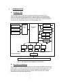
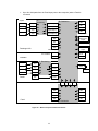
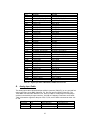
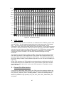
1
FASTSERIES FASTIMAGE 1300 HARDWARE USER’S MANUAL FAST CAPTURE FAST PROCESSING FAST RESULTS FASTSERIES PCI BOARD FAST SERIES PMCs FastVision FastImage 1300 FastFrame 1300 FastMem Fast4 1300 Fast I/O 1300 30002-00176 COPYRIGHT NOTICE Copyright 2002 by Alacron Inc. All rights reserved. This document, in whole or in part, may not be copied, photocopied, reproduced, translated, or reduced to any other electronic medium or machine-readable form without the express written consent of Alacron Inc. Alacron makes no warranty for the use of its products, assumes no responsibility for any error, which may appear in this document, and makes no commitment to update the information contained herein. Alacron Inc. retains the right to make changes to this manual at any time without notice. Document Name FastImage 1300 Hardware User’s Manual Document Number: 30002-00176 Revision History: 2.0 June 4, 2002 Trademarks: Alacron is a registered trademark of Alacron Inc. AltiVec is a trademark of Motorola Inc. Channel Link is a trademark of National Semiconductor CodeWarrior is a registered trademark of Metrowerks Corp. FastChannel is a registered trademark of Alacron Inc. FastSeries is a registered trademark of Alacron Inc. Fast4 , FastFrame 1300 , FastImage , FastI/O , and FastVision are registered trademarks of Alacron Inc. FireWire is a registered trademark of Apple Computer Inc. 3M is a trademark of 3M Company MS DOS is a registered trademark of Microsoft Corporation SelectRAM is a trademark of Xilinx Inc. Solaris is a trademark of Sun Microsystems Inc. TriMedia is a trademark of Philips Electronics North America Corp. Unix is a registered trademark of Sun Microsystems Inc. Virtex is a trademark of Xilinx Inc. Windows , Windows 95 , Windows 98 , Windows 2000 , and Windows NT are trademarks of Microsoft Corporation All trademarks are the property of their respective holders. Alacron Inc. 71 Spit Brook Road, Suite 200 Nashua, NH 03060 USA Telephone: 603-891-2750 Fax: 603-891-2745 Web Site: http://www.alacron.com/ Email: [email protected] or [email protected] TABLE OF CONTENTS Copyright Notice ……………………………………………………………………………….. Table of Contents …………………………………………………………………………….... Manual Figures & Tables ……………………………………………………………………… Other Alacron Manuals ………………………………………………………………………… I. ii iii vi vii INTRODUCTION................................................................................................................................ 1 A. FastImage 1300 ........................................................................................................................... 1 B. Processors and Memory ............................................................................................................. 1 C. 1. 2. 3. 4. Analog and Digital Input............................................................................................................ 2 Analog Input ................................................................................................................................. 2 Digital Input.................................................................................................................................. 2 Digital Control Inputs ................................................................................................................... 2 Digital Control Outputs................................................................................................................. 3 1. 2. 3. Other Inputs and Outputs.......................................................................................................... 3 Analog Output............................................................................................................................... 3 FastChannel Digital Input/Output ................................................................................................. 3 Channel Link Input/Output ........................................................................................................... 4 D. E. PMC Daughter Cards................................................................................................................. 4 F. Local PCI Bus ............................................................................................................................. 4 II. THEORY OF OPERATION............................................................................................................ 5 A. Camera Types ............................................................................................................................. 5 B. 1. 2. Analog Video Input..................................................................................................................... 5 NTSC/PAL Composite and S-Video Component Input................................................................ 6 Monochrome and RGB Analog Video Input ................................................................................ 7 1. 2. Digital Input ................................................................................................................................ 7 Digital Control Inputs ................................................................................................................... 8 Camera Controls ........................................................................................................................... 8 1. 2. 3. 4. 5. 6. 7. FPGA-Based Front End ............................................................................................................. 9 FPGA Run States ........................................................................................................................ 10 Input Signals from Line Cameras to FPGA ................................................................................ 10 Input Signals from Frame Cameras to FPGA.............................................................................. 11 NTSC/PAL/S-Video Input Signals ............................................................................................. 11 Data Reordering.......................................................................................................................... 12 Image Distribution ...................................................................................................................... 12 Data Valid Signals ...................................................................................................................... 12 C. D. E. Digital Crosspoint Switch......................................................................................................... 13 F. 1. 2. 3. 4. 5. 6. 7. 8. 9. Processors and Memory ........................................................................................................... 15 TriMedia Processors ................................................................................................................... 16 Local SDRAM ............................................................................................................................ 16 Video Data Paths ........................................................................................................................ 16 Local PCI Bus............................................................................................................................. 17 Interprocessor Communication ................................................................................................... 17 Audio Input and Output .............................................................................................................. 17 Interrupts..................................................................................................................................... 18 TriMedia Configuration EEPROM............................................................................................. 20 Peripheral Controls ..................................................................................................................... 20 iii G. FastChannel Digital Input/Output .......................................................................................... 20 H. Analog Output........................................................................................................................... 22 I. PCI-PCI Bridge............................................................................................................................. 22 J. PMC Slots...................................................................................................................................... 23 K. CPLD ......................................................................................................................................... 23 L. UART and Serial Port .............................................................................................................. 23 M. Power ......................................................................................................................................... 23 N. Clock Distribution..................................................................................................................... 24 IQ32B Pins, Ports, and Signals ................................................................................................... 26 1. III. CONNECTORS AND JUMPERS ................................................................................................. 28 A. 1. 2. 3. 4. 5. 6. 7. Connectors................................................................................................................................. 28 Rear Bracket Connectors ............................................................................................................ 28 Analog and Digital Input Connector (J1A/J1B).......................................................................... 29 Analog/ChannelLink/RS-232 Connector (J2) ............................................................................. 30 FastChannel Digital Input/Output (J4, J5) .................................................................................. 31 PMC Slots (J1, J3) ...................................................................................................................... 31 Power .......................................................................................................................................... 32 Test Connectors .......................................................................................................................... 32 1. 2. 3. 4. 5. Jumpers ..................................................................................................................................... 33 P3................................................................................................................................................ 33 P4................................................................................................................................................ 33 P9................................................................................................................................................ 34 P14.............................................................................................................................................. 34 P16.............................................................................................................................................. 34 B. IV. FASTIMAGE 1300 CABLES ........................................................................................................ 35 A. Cable Summary......................................................................................................................... 35 B. Power Cables............................................................................................................................. 35 C. Digital Input Cable ................................................................................................................... 35 D. Analog Input Cable................................................................................................................... 37 E. ChannelLink/TV/RS-232 Cable............................................................................................... 38 F. NTSC/TV Out Cable ................................................................................................................ 39 G. FastChannel Digital I/O Output (J4, J5) ................................................................................ 39 V. PROGRAMMING, CONFIGURATION, AND TEST.................................................................. 40 A. I2C Bus ...................................................................................................................................... 40 B. 1. 2. V.34 SSI Interface (TM1 to CPLD)......................................................................................... 40 Serial Communication Port (UART) .......................................................................................... 41 FPGA Serial Programming ......................................................................................................... 41 1. 2. 3. JTAG Chains............................................................................................................................. 42 JTAG Chain #1 - Boundary Scan 21150 Bridge Chip and SAA7111A EVIP............................ 42 TriMedia JTAG Chain #2 - TriMedia Processors....................................................................... 42 JTAG Chain #3 – CPLD, FPGA1, FPGA2, Crosspoint FPGAs, and IQ32B ............................. 43 C. VI. A. CPLD SPECIFICATION .............................................................................................................. 44 V.34 SSI Interface..................................................................................................................... 44 iv B. JTAG Interface ......................................................................................................................... 45 C. External Five-Wire Interface................................................................................................... 45 D. PCI Bus Secondary Clock Mask.............................................................................................. 46 E. Low-Speed Timing Functions .................................................................................................. 46 F. 1. CPLD Programming Requirements ........................................................................................ 47 Address (Hex) Description ......................................................................................................... 48 VII. UART Specification ....................................................................................................................... 51 A. Purpose ...................................................................................................................................... 51 B. Features ..................................................................................................................................... 51 C. I2C Address................................................................................................................................ 51 D. Interrupts................................................................................................................................... 51 E. 1. 2. 3. 4. 5. 6. 7. Register descriptions................................................................................................................. 52 Subaddress 00, Write – UART Control Register ........................................................................ 52 Subaddress 00, Read - UART Status Register ............................................................................ 53 Subaddress 01, Write – Transmit Data Register ......................................................................... 54 Subaddress 01, Read – Receive Data Register............................................................................ 54 Subaddress 02, Write – Ports A / B latch.................................................................................... 54 Subaddress 02, Read – Ports A / B Pins ..................................................................................... 54 Subaddresses 03-FF – PIC Register File..................................................................................... 55 VIII. Specifications ............................................................................................................................. 56 A. Processors .................................................................................................................................. 56 B. NTSC/PAL Composite Video Capture.................................................................................... 56 C. Analog Video Capture .............................................................................................................. 56 D. Digital Video Capture............................................................................................................... 57 E. Digital Video Output ................................................................................................................ 57 F. Camera Control ........................................................................................................................ 57 G. Analog Video Output................................................................................................................ 57 H. Monitor Output......................................................................................................................... 58 I. PCI Interface................................................................................................................................. 58 J. PMC Interface............................................................................................................................... 58 IX. TROUBLESHOOTING ................................................................................................................. 59 X. ALACRON TECHNICAL SUPPORT........................................................................................... 60 A. Contacting Technical Support ................................................................................................. 60 B. Returning Products for Repair or Replacements................................................................... 61 C. Reporting Bugs.......................................................................................................................... 62 v MANUAL FIGURES & TABLES FIGURE PAGE SUBJECT TABLE PAGE SUBJECT 1 2 3 4 5 6 7 8 9 10 11 12 13 14 15 16 17 18 19 20 21 22 1 5 6 7 9 10 11 11 12 14 16 17 18 19 20 22 25 28 40 45 47 47 Block Diagram of the FI1300 Data Flow of the FastImage Analog Video Input Digital Video Input Camera Control Output Signal Front End Comp & Data Flow Line Camera Input Signals Digital Frame Camera Input S. NTSCPAL/S Video Input S. Main Crosspoint Switch Conn. Processors and Memory Message Passing Connection Audio Connections Interrupts FastChannel Input/Output Analog Output IQ32B Clock Distribution FI1300 Front Panel Bracket Configuration & Control V.34 Interface Timing Low-Speed Timing Signals, Ex Low-Speed Timing Signals, Fr 1 2 3 4 5 6 7 8 9 10 11 12 13 14 15 16 17 18 19 20 21 22 23 24 6 7 21 21 26 29 30 31 32 32 33 33 33 34 34 34 36 37 38 38 38 39 48 49 Composite Analog Video Inputs 8 Bit Analog Input Channel FastChannel Interface Controls I/O Expander Registers IQ32B Signals A/D Input Connector J1A/J1B Analog Output/CL/RS232 Conn. FastChannel Digital I/O Conn. PMC-PN4 Connectors J1/J3 Test Connector P10 Test Connector P11 Test Connector P12 Jumper P3 Jumper P9 Jumper P14 Jumper P16 Digital Input Cable, DSUB37 P2 Digital Input Cable, DSUB37 P3 Analog Input Cable NTSC/S Video Conn P2 & P3 RS-232 Connector P4 SVGA (RGB) Output Conn P5 Control Register Bits Crosspoint Control register vi OTHER ALACRON MANUALS Alacron manuals cover all aspects of FastSeries hardware and software installation and operation. Call Alacron at 603-891-2750 and ask for the appropriate manuals from the list below if they did not come in your FastSeries shipment. • 30002-00146 FastImage and FastFrame HW Installation for PCI Systems • 30002-00148 ALFAST Runtime Software Programmer’s Guide & Reference • 30002-00150 FastSeries Library User’s Manual • 30002-00153 Fast I/O Hardware User’s Manual • 30002-00155 FastMem Hardware User’s Manual • 30002-00162 FOIL – FastSeries Object Imaging Library User’s Manual • 30002-00169 ALRT Runtime Software Programmer’s Guide & Reference • 30002-00170 ALRT, ALFAST & FASTLIB Software Installation Manual for Linux • 30002-00171 ALRT, ALFAST, & FASTLIB Software Installation for Windows NT • 30002-00172 FastImage 1300 Hardware User’s Manual • 30002-00173 FastMem Programmer’s Guide & Reference • 30002-00174 FastMem Hardware Installation Manual • 30002-00180 Fast4 1300 Hardware User’s Manual • 30002-00184 FastSeries Getting Started Manual • 30002-00185 FastVision Hardware Installation Manual • 30002-00186 FastVision Software Installation Manual vii I. INTRODUCTION A. FastImage 1300 The FastImage1300 is an autonomous imaging system that can process up to four continuous video streams with minimal impact on the Host system. The FastImage1300 system consists of a main board with one to four TriMedia TM1300 PCI media processors and memory. Options include analog or digital input via a frame buffer, unbuffered digital I/O, Channel Link I/O, analog output, and one or two PMC daughter cards. 24 bits RS-170 or RGB Analog Input NTSC/PAL/Svideo Analog Input Front End FPGAs + Frame Buffer FastChannel Digital I/O CROSSPOINT FPGAs Channel Link Output Channel Link Input 32 bits Digital Input Fast Channel APMC Fast Channel PMC1 Analog Output TM1 DRAM TM3 TM2 DRAM DRAM TM4 DRAM Internal PCI Bus FastImage1300 Board PCI Bridge Host System PCI Bus Figure 1. Block Diagram of the FI1300 Board in a PC Chassis B. Processors and Memory The FastImage 1300 can be configured with one or four Trimedia 1300 DSP processors (TM1 through TM4). The crosspoint switch eliminates the need to bypass missing processors’ video paths, however zero ohm resistors will be required to complete the JTAG data loop in oneCPU systems. Sensing resistors will also be included to allow the bridge chip to disable unused clock lines on the secondary PCI bus. 1 Reducing the number of processors also reduces the input bandwidth of the board. The total input bandwidth is limited to 80 MB/s per installed processor. Also, systems with just one processor will have one master clock output instead of two. Each processor can have 8MB, 16MB, 32MB or 64MB of dedicated SDRAM. All TMs on a given board must have the same amount of SDRAM. C. Analog and Digital Input The board has four inputs, TAP1 through TAP4; each TAP consists of 8 bits data, 2 bits control, and pixel clock. A TAP can be configured for analog input or for digital input (but not both). TAP1 through TAP3 can be populated as either digital input or RS170 compatible analog input. TAP4 can be either digital input or composite analog input (NTSC/PAL/SECAM or S-Video). Analog and digital video capture signals come in through the same dual 68-pin VHDCI connector, J1A/J1B. In order to save pins, analog and digital signals share pins, allowing only one or the other for each of the four input taps. Inputs from the four TAPs go to the Front End FPGAs with their associated frame buffers, and then are routed via the crosspoint to the TriMedia or FastChannel. 1. Analog Input Four RS-170 level video inputs allow selection from four composite video sources. The same inputs can also be used in pairs to receive S-video signals. Note that only one composite/component video stream can be captured at one time. These inputs are multiplexed into a common converter (two converters in S-video mode). The primary 2 TM1300 controls the input selection using the I C bus to access the internal registers of the SAA7111A. Three additional RS-170 level video inputs can be used to capture images from three additional monochrome cameras or one RGB camera. Sync detection circuitry for these inputs is very flexible, allowing the use of asynchronous reset cameras as well as interlaced or progressive area scan cameras and line scan cameras. 2. Digital Input Digital video input lines allow direct connection of digital line-scan or area-scan cameras of up to 32 bits. The 32 Digital data inputs are received by high-speed RS422 differential receivers whose outputs are run through the FPGA-based front end to standard I/O’s on the crosspoint switch. The switch can then route these to the data inputs of the TM1300 processors or the digital video input port of the S3 Virge GX2. All digital video data and control signals are differential RS-422 level signals with proper termination for twisted pair cable. High-speed line drivers and receivers are used on all digital signals, however the RS-422 standard was not designed for very high data rates. Thus the interface circuitry may limit the maximum practical data rate to considerably less than the 80 MHz video input bandwidth of the TriMedia chips unless the receivers are upgraded to the LVDS model. Industry standard pin-out devices are used for all RS422 receivers and drivers (26LS31 and 26LS32 footprint) to allow upgrade to faster parts as required. LVDS interface drivers and receivers are available as selective stuffing options. 3. Digital Control Inputs Four special clock inputs are provided. These inputs are received by high-speed RS422 differential receivers. The outputs of these receivers go to dedicated global clock inputs of the FPGA. Programmable clock polarity and input delay allow compensation for clock to data skew. 2 Eight additional control inputs are provided. These inputs are received by high-speed RS422 differential receivers. The outputs of these receivers go to the FPGA. These lines may be used for frame valid and line valid signals when attaching multiple cameras. Four general purpose static inputs are provided. These inputs are received by RS422 differential receivers. The outputs of these receivers can be read directly by the primary 2 TM1300 via the I C bus. 4. Digital Control Outputs Two outputs are provided for line or frame start. These RS422 differential outputs are intended for uses with line scan or area scan cameras that require a scan start pulse. They are generated in the CPLD in response to external trigger inputs (after a programmed delay) or on command of the primary TM1300. Two outputs are provided for exposure control. These RS422 differential outputs are intended for uses with line scan or area scan cameras, which require a scan, start pulse. They are generated in the CPLD in response to external trigger inputs (without a delay) or on command of the primary TM1300. Camera exposure time is controlled by the delay between these signals and the line / frame start signals. Two master clock outputs are provided to generate a time base for cameras. These RS422 differential outputs are intended for use with line scan or area scan cameras, which require an external time base. They are generated by the primary and secondary TM1300’s using the AI_OSCLK outputs. Only one of these signals is available on the single processor model. These pins can generate any frequency from 1 Hz to 40 MHz in .07 Hz steps using the direct digital synthesizer of the TM1300. Nominal jitter on these outputs due to digital synthesis is 3.3 nanoseconds. This will be reduced to less than 1 nanosecond in the TM1300 when the improved mode is used. In TM1300 improved mode, the frequency resolution is 0.3 Hz. Four general purpose static outputs are provided. These RS422 differential outputs can 2 be written directly by the primary TM1300 via the I C bus. D. Other Inputs and Outputs The system can be configured with analog output, FastChannel input/output, Channel Link input/output, or with no output. 1. Analog Output Analog output can drive the system SVGA display and also provide NTSC TV output to a monitor. SVGA monitor signals go out through 68-pin high-density connector J2. Composite and Svideo outputs, and the RS-232 port also share connector J2 and Channel Link. Systems that have another video adapter in addition to the onboard S3-based SVGA can use the host’s adapter and monitor to display video output in one or more possibly overlapping windows. The TM1300 supports this functionality directly via the image coprocessor unit. When using the onboard S3 SVGA, processed image data can be scaled and alpha blended as well. 2. FastChannel Digital Input/Output The FastChannel interface provides 32 bits of digital input and output directly to and from the crosspoint via connectors J4 and J5 on the top edge of the board. The interface includes 32 bits of RS422 or LVDS differential digital output drivers and receivers, with RS422 digital video control and clock inputs/outputs. 3 3. Channel Link Input/Output The FastImage1300 implements the 28-bit Channel Link digital I/O interface as an option. Compatible cameras or other input devices can be connected directly to the Channel Link inputs. Channel Link outputs may be connected to another FastImage1300 for high-speed inter-board communication. E. PMC Daughter Cards Two PMC slots connect to the FastImage internal PCI bus via standard PMC connectors and to the crosspoint switch via the Alacron FastChannel connector. Daughter cards from Alacron are available to extend the I/O, memory, or processing power of a FastImage board via the PMC slots and FastChannel. • Fast4 daughter card supplies one to four additional TriMedia processors. • FastIO daughter card supplies additional digital or analog I/O. • FastMem daughter card supplies up to 512MB of global SDRAM. Each of these products is described in its own documentation set. F. Local PCI Bus All other data into and out of the FastImage use the PCI bus. High-speed devices such as IEEE 1394 FireWire connect to the secondary PCI bus via the PMC expansion connectors. Additional devices can be connected to the host’s primary PCI bus. 4 II. THEORY OF OPERATION This chapter describes the camera connections, internal data flow paths, and other functional components of the FastImage board. PMC1 Camera Front End PMC2 FastChannel I/O Crosspoint Switch S3 VGA/TV Outputs TriMedias Figure 2. Data Flow in the FastImage Input data from the camera is converted (as needed) into RGB or YUV digital data by the front end and distributed to the TriMedia processors via the crosspoint. Output data from the TriMedia goes via the crosspoint to the S3 SVGA/TV outputs, and can also be routed among the TriMedia and to and from PMC daughter cards. The FastChannel I/O connects directly to the crosspoint as a separate source or as a destination for TriMedia output. A. Camera Types A camera can be digital or analog, line or frame, single- or multi-tap. Common configurations are: B. • Three 8-bit RS-170 cameras plus one NTSC/PAL/S-Video camera. • Four 8-bit asynchronous digital cameras (quad single-tap) • Two 16-bit digital cameras (dual two-tap) • One 32-bit digital camera (single four-tap) Analog Video Input Analog video capture signals come in the dual 68-pin VHDCI connector J1A/J1B. Three 8-bit RS-170 level video inputs can be used to capture images from three monochrome cameras or one RGB camera. Each channel has sync detection and pixel clock generation to allow simultaneous acquisition from three independent (non-genlocked) sources. Sync and pixel clocks may also be driven from an external RS-422 source. Independent offset and gain controls are available for each of the three channels. Output from the A/D converters can be further processed in the FPGA-based digital front end. 5 8 bits RS-170 A/D 8 bits RS-170 A/D TAP2 8 bits RS-170 A/D TAP3 EVIP TAP4 NTSC/PAL/S-Video TAP1 Figure 3. Analog Video Input 1. NTSC/PAL Composite and S-Video Component Input A Philips SAA7111A Enhanced Video Input Processor digitizes composite or S-video from any source adhering to the NTSC, PAL or SECAM standards for 525-line 59.94 Hz and 625-line 50 Hz video. The chip has four inputs VID1 through VID4 as shown in Table 1. Each input can receive a separate composite video sources, one of which is selected to be sent through the processors. Two S-video sources can be connected (Y on VID1,UV on VID3 or Y on VID2, UV on VID4), one of which is the selected input. These inputs are multiplexed into a common converter (two converters in S-video mode). The primary 2 TriMedia controls the input selection using the I C bus to access the SAA7111A registers. J1B Pins J1B Signal Analog In to EVIP EVIP Input Pin 58, 59 TAP4_D0, GND VID1 AI11 56, 57 TAP4_D1, GND VID2 AI12 54, 55 TAP4_D2, GND VID3 AI21 52, 53 TAP4_D3, GND VID4 AI22 Table 1. Composite Analog Video Inputs The SAA7111A outputs 8-bit parallel digitized video encoded per ITU-R BT.656, which can be directly acquired by the TriMedia processors, or the S3 Virge GX2. The pixel rate is phase locked to the horizontal scan rate of the input image and is nominally 13.5 MHz. Since each pixel requires 16 bits of data, the data output clock rate is 27 MHz. Color video requires three values per pixel. NTSC and PAL use Y (luminance) Cr (red portion of chroma) and Cb (blue portion of chroma). For eight-bit resolution of each component, 24 bits per pixel would be required. The pixel size of 16 bits (rather than 24 bits) is realized by sub-sampling the chroma portion of the input signal per ITU-R BT.601 (ITU recommendation - broadcast television 601, formerly known as CCIR601) 13.5 MHz 4:2:2 encoding standard. The mnemonic 4:2:2 refers to the fact that for every four pixels, luminance (Y) is sampled four times, while chroma (Cr and Cb) components are only sampled twice. This sub-sampling is in line with the chroma bandwidth limits of the NTSC / PAL standards and does not cause a degradation of picture quality. 6 2. Monochrome and RGB Analog Video Input Three 8-bit A/D converters are available for three channels of RS170 compatible monochrome video or one RGB video source in parallel with the EVIP. Each channel has associated sync detection and pixel clock generation to allow simultaneous acquisition from three independent (non-genlocked) sources. Sync and pixel clocks may also be driven from an external RS-422 source. Independent offset and gain controls are available for each of the three channels. Maximum conversion rate (pixel clock) is 80 Mpixels/s. Pins Signal J1A-10, J1A-11 TAP1-D0, GND J1A-58, J1A-59 TAP2-D0, GND J1B-10, J1B-11 TAP3-DO, GND Table 2. 8-Bit Analog Input Channels Output from the A/D converters can be further processed in the FPGA-based front end. Multitap operation is described later in the section on the Front End. C. Digital Input Video capture signals come in through a dual 68-pin VHDCI connector (J1A/J1B). To save pins, analog and digital signals share pins allowing only one or the other for each of the four input taps. Digital video input lines allow direct connection of digital line-scan or area-scan cameras of up to 32 bits. All digital video data and control signals are differential RS-422 level signals with proper termination for twisted pair cable. High speed line drivers and receivers are used on all digital signals. Industry standard pin-out devices are used for all RS422 receivers and drivers to allow upgrade to faster parts as required. LVDS and PECL interface drivers and receivers are available as selective stuffing options. 8 bits Data, CLK, LVAL, FVAL TAP1 8 bits Data, CLK, LVAL, FVAL TAP2 8 bits Data, CLK, LVAL, FVAL TAP3 8 bits Data, CLK, LVAL, FVAL TAP4 Figure 4. Digital Video Input 7 1. Digital Control Inputs Four clock inputs (TAPn_PIXCK) come in through the input connector J1A/J1B. These inputs are received by high-speed RS422 differential receivers. The outputs of these receivers go to the crosspoint. PIX_CLK1 should be used for multi-tap cameras requiring both FPGAs. Programmable clock polarity and input delay allow compensation for clock to data skew. Eight additional control inputs (TAPn_LVAL and TAPn_FVAL) come in through the Digital input connector J1A/J1B. These inputs are received by high-speed RS422 differential receivers. The outputs of these receivers (LVALn, FVALn) go to the FPGAs; LVAL/FVAL1 and 3 go to both FPGAs, LVAL/FVAL2 and 4 go to FPGA 1 only. These lines may be used for frame valid and line valid signals when attaching multiple cameras. Four general purpose static inputs (GPINn) are provided. These inputs are received by RS422 differential receivers. The outputs of these receivers go to the UART, where they 2 can be read by the primary TriMedia via the I C bus. 2. Camera Controls Camera Controls are outputs sent back through the digital input connector J1A/J1B. Three kinds of controls are available: start and exposure signals, master clocks, and general purpose control signals. a) Frame/Line Start and Exposure Four strobe lines, STROBE1-STROBE4, are output to connector J1A/J1B. These RS422 differential outputs are for line scans or area scans cameras that require a scan start pulse, readout, or exposure control signals (e.g., EXSYNC and PRIN to Dalsa cameras). The CPLD has two counters for generating line/frame start and exposure timing signals (Figure 5). These 9-bit counters run at 10 KHz, allowing timing from 100 microseconds to 50 milliseconds. The counters are triggered by the rising edge of one of the two EXT_TRIGn inputs from J1A/J1B. Upon triggering, they count up from zero and stop when they reach maximum count (511). Two 9-bit compare registers, COMP1 and COMP2, are associated with each counter. These are programmed to create timing events from 1 to 512 clock cycles after the trigger. In normal usage the value of COMP1 is less than that of COMP2. Four output signals per counter, Cmp1, Cmp1Pls, Cmp2, and Cmp2Pls, are run to the crosspoint where they can be selected to run to the four strobe lines. Signals Cmp1Pls and Cmp2Pls are active high pulses, 100 microseconds wide, beginning at the times programmed in COMP1 and COMP2. Cmp1 is an active high pulse, which starts at the trigger and ends at the time programmed into COMP1. Cmp2 is an active high pulse starting at the time programmed into COMP1 and ending at the time programmed into COMP2 (note that if COMP2 is less than COMP1 this signal will begin during one trigger cycle and end during the next). The counters cannot be retriggered while running until the time programmed into COMP2 has elapsed. The camera control signals provide a flexible control interface. In a typical application, a Cmp1 signal could be used to start camera exposure. The corresponding Cmp2 signal could initiate transmission of the camera data to the FastImage. The four external strobe signals on J1A/J1B output the Cmp1 and Cmp2 signals from the two counters. STROBE1 outputs Counter1 Cmp1, STROBE2 outputs Counter1 Cmp2. STROBE3 outputs Counter2 Cmp1, and STROBE4 outputs Counter2 Cmp2. 8 No Retrigger Trigger Cmp1 Cmp1Pls Cmp2 100 µSec Cmp2Pls Time = 0 COMP1 COMP2 Figure 5. Camera Control Output Signals b) Master Clocks Four master clock outputs (MASTER_CKn) to connector J1A/J1B are provided to generate a time base for cameras. These RS422 differential outputs are intended for use with line scan or area scan cameras, which require an external time base. Master clock outputs are generated by the primary and secondary TriMedias using the AI_OSCLK outputs. Only one clock source is available on the single processor model. These pins can generate any frequency from 1 Hz to 40 MHz in .07 Hz steps using the direct digital synthesizer of the TriMedia. Nominal jitter on these outputs due to digital synthesis is 3.3 nanoseconds. This is reduced to less than 1 nanosecond in the TM1300 when the improved mode is used. In TM1300 improved mode, the frequency resolution is 0.3 Hz. c) General-Purpose Outputs Four general purpose static outputs (GPOUT0-3) are provided to connector J1A/J1B. These RS422 differential outputs can be written out through the UART by the primary 2 TriMedia (via the I C bus). D. FPGA-Based Front End Digital data inputs pass through two FPGAs, each with an external SDRAM. The FPGAs can perform multiplexing and re-order incoming data for Odd/Even and Left/Right tapped cameras. Data is divided into two 16-bit halves, one to each FPGA. When using three or four tap cameras, half the bits from each tap are routed to each FPGA, allowing the two parts to operate identically. When using multiple smaller cameras, each FPGA services a different camera or pair of cameras. These FPGAs are in-system reprogrammable, allowing application-specific operations to be performed. 9 Tap1[0:3] Normal/ Multitap TAP1[0:7] FPGA1 Frame Buffer Normal: Tap1[4:7] Multitap:Tap3[0:3] Tap2[0:3] 8 FPGA1_DO0 To Crosspoint 8 Normal: Tap2[4:7] Multitap:Tap4[0:3] TAP2[0:7] Tap3[4:7] FPGA1_DO1 FPGA2 TAP3[0:7] Normal: Tap3[0:3] Multitap:Tap1[4:7] Frame Buffer Tap4[4:7] TAP4[0:7] 8 Normal: Tap4[0:3] Multitap:Tap2[4:7] 8 FPGA2_DO2 To Crosspoint FPGA2_DO3 Figure 6. Front End Components and Data Flow 1. FPGA Run States The input FPGAs control the operation. This section is a general description of the FPGA’s capabilities, not specific to any application. The FPGA has two states: stopped and running. When the FPGA is stopped, no data flows in from any source. When the FPGA is running, data flows in from the selected source. The data units can be one of three sizes: pixels, lines, and frames. A Transfer Counter (TC) internal to the FPGA counts the data units as specified in the program. When the FPGA is stopped, the TC is empty. To change from stopped to running, the program loads a number into the TC. Two running modes are Fixed and Continuous. • In fixed running mode, the Transfer Counter receives a number of units, and counts down as each pixel, line, or frame is clocked in. When the TC counts down to zero, the FPGA changes back to the stopped state. • In continuous running mode, the TC receives a maximum initial value, which is also stored in a shadow register. Each time the TC counts down to zero, it is automatically reloaded from the shadow register and running continues. In both fixed and continuous modes, an end-of-word, end-of-line, or end-of-frame indication is available to the FPGA. 2. Input Signals from Line Cameras to FPGA For digital line cameras, the Data, Line Valid, and CLK input signals come directly from the digital input drivers. For analog line cameras, the input data and controls go through the A/D converters to be converted to the Data, Line Valid, and CLK signals for the FPGA. LVAL1, 2, and 3 go to FPGA 1; LVAL1, 3, and 4 go to FPGA2. A linear region of interest may be specified as begin and end points (X, Y). To accommodate variations in camera timing, the ROI may be specified as a negative value or as a point beyond the upper limit of the line. 10 Data 8 FPGA Region of Interest 0 Line Valid X 1023 Y CLK To Crosspoint Figure 7. Line Camera Input Signals and Region of Interest 3. Input Signals from Frame Cameras to FPGA Data 8 SP FPGA EP Region of Interest Frame Valid SL Line Valid EL CLK To Crosspoint Figure 8. Digital Frame Camera Input Signals and Region of Interest For digital frame cameras, the Data, Line Valid, Frame Valid, and CLK input signals come directly from the digital input drivers. For analog frame cameras, the input data and controls go through the A/D converters to be converted to the Data, Line Valid, Frame Valid, and CLK signals for the FPGA. LVAL1/FVAL1, 2, and 3 go to FPGA 1; LVAL1/FVAL1, 3, and 4 go to FPGA2. A rectangular region of interest may be specified as a rectangle with start and end pixels (SP, EP) and start and end lines (SL, EL). To accommodate variations in camera timing, the ROI may be specified using negative values or outside the frame boundaries. 4. NTSC/PAL/S-Video Input Signals Composite or component video input to the SAA7111 Enhanced Video Input Processor (EVIP) is converted to YUV data that can be processed directly by the TriMedia. The EVIP provides Frame Valid and Odd/Even field signals. 11 NTSC/PAL or S-Video EVIP YUV Data FPGA Frame Valid Odd/Even Field Figure 9. NTSC/PAL/S-Video Input Signals 5. Data Reordering Data from Multitap cameras is re-ordered using the SDRAM. Incoming data is formed into groups of two 32-bit words inside each FPGA and written to the SDRAM location corresponding to its desired position in the output image. When a complete image has been buffered in the SDRAM, it is read out to the TM1300s while the next image is buffered in the other half of the SDRAM. Four pairs of words are read then four pairs written to reduce the buffering requirements of the FPGA while keeping the SDRAM running near its optimal burst rate. Depending on the FastImage1300 inputs, the application may require a reordering of the data coming in to the Front End from Taps 1, 2, 3, and/or 4 and exiting the Front End as data bytes FPGA1_DO[0:7], FPGA1_DO[8:15], FPGA2_DO[0:7], and FPGA2_DO[8:15]. The mapping of input taps to FPGA data bytes is diagrammed in area A of the FastImage1300 crosspoint Figure 14. Each tap can connect to one or more of FPGA1_DO[0:7] through FPGA2_DO[8:15]. Multiple input taps can be multiplexed to one FPGA_DO data byte. Unused taps can be left unconnected. 6. Image Distribution When the incoming data exceeds the input bandwidth of a single TriMedia processor (80 to 320 MB/s), the images are distributed among multiple processors. One processor receives the first image and the other receives the second image. Image distribution affects the buffering requirement in the front end. Due to banking restrictions of the SDRAM, multiple frames must be buffered when distributing images to multiple CPUs. Two image buffers are required for each CPU used. Thus when four TM1300s are needed to handle the input bandwidth requirements, eight frames must be buffered. This condition limits the frame size to 1/8 of the frame buffer or 2 megabytes. 7. Data Valid Signals Four data valid signals are generated by the FPGAs, one for each TriMedia. Each signal is synchronous to the video input clock of the associated TriMedia. Each signal connects to the VI_DVALID pin of the TriMedia via the crosspoint to match the delay time of the data lines. The data valid signals synchronize the data capture to the valid pixels from the camera in raw capture modes. When using synchronous data buffering in the crosspoint, the position of the data valid relative to the pixel data can be adjusted by varying the number of flip-flop stages each goes through in the crosspoint input buffer. Region of interest capture can be handled in the FPGA if logic cells and routing are available. 12 Another purpose of the data valid is to pad (or truncate) the frame to a multiple of 64 pixels. This allows use of cameras with non-binary height and width. The 64 pixel limitation comes from the TriMedia, which must define buffers in 64 byte increments. Providing dummy (garbage) pixels at the end of the frame to fill out the buffer greatly simplifies programming in TriMedia raw capture modes. Padding is accomplished with a 6-bit (modulo 64) counter, which runs only when data valid is active. If the contents of the counter are not zero when the next frame sync arrives, data valid is asserted until the counter rolls over to zero. Note that this requires the frame synch signal to precede the first valid pixel by up to 63 clock cycles depending on the number of pixels in a frame. This is not necessary for cameras with a multiple of 64 pixels per frame (most line scan cameras and square format area scan cameras) since the counter will be at zero after the last pixel of the frame. E. Digital Crosspoint Switch Two Xilinx Virtex XCV50 FPGAs form a switch matrix with flexible I/O buffers at each port. These parts also contain distributed RAM for buffering data as required. Multiplexers can match the input data bus width to the TriMedia processors. Demultiplexers can match TriMedia video output to the digital output bus. In addition to the main data switch matrix, a smaller switch (I-Cube IQ32B) is used for flexible routing of clock signals with low latency and skew. Configuration of the crosspoint switch matrix is SRAM-based, allowing reconfiguration in system. Configuration data is downloaded to the part via a standard JTAG port. Because of the relatively slow rate of configuration, the crosspoint switch is used as a static interconnect for most applications. The JTAG bit stream data can be generated by tools available from Xilinx. The main crosspoint switch is the connection among the sources and destinations. Sources are defined as inputs to the crosspoint: • Four 8-bit input paths from the FPGAs to the crosspoint. • Four 8-bit paths from the Video Output of each TriMedia to the crosspoint • Four 8-bit paths from the FastChannel digital inputs to the crosspoint. • Three or four 8-bit paths from the FastIO input ports to the crosspoint (when a FastIO is connected). Port A can be set as either input or output; Ports B, C, and D are always inputs to the crosspoint. • Two 8-bit paths from the FastMem input ports C and D to the crosspoint (when a FastMem is connected). • Up to four 8-bit paths from the Fast4 input ports to the crosspoint (when a Fast4 is connected. Destinations are defined as outputs from the crosspoint: • Four 8-bit paths from the crosspoint to the Video Input of each TriMedia. • One 16-bit path from the crosspoint to the S3 GX2 for VDA and TV analog outputs • Four 8-bit paths from the crosspoint to the FastChannel digital outputs. • One 8-bit path from the crosspoint to the FastIO output port (when a FastIO is connected). Port A must be set as output from the FastImage1300 to the FastIO. • Two 8-bit paths from the crosspoint to the FastMem output ports A and B (when a FastMem is connected). 13 • Up to four 8-bit paths from the Fast4 input ports to the crosspoint (when a Fast4 is connected. Inputs A. Reordering B. Distribution Tap1 fpga1 DO[0:7] Tap2 fpga1 DO[8:15] Tap3 fpga2 DO[0:7] Tap4 fpga2 DO[8:15] Input Taps Front End Outputs TM0 TM1 TM2 TM3 TriMedia Inputs FastChannel Digital Input/ Output TM0 TM1 Channel Link I/O TM2 TM0 FastImage1300 VGA & TV Output TriMedia Outputs From FastMem PortC PortA PortD PortB FastMem To FastMem C. Reordering Tap1 TM0 PortA Tap2 PortA Tap3 TM0 PortB Tap4 PortD FastIO TM0 PortC A Fast4 B D TM0 TM0 TM1 TM1 TM2 TM2 TM3 TM3 D. Distribution Figure 10. Main Crosspoint Switch Connections 14 C The mapping of data sources to destinations is diagrammed in area B of the crosspoint diagram above. Any source can connect to one or more destinations. No two sources can be connected to (i.e., drive) the same destination. The sources and destinations include any PMC daughter cards that are connected to the FastChannel PMC slots. An installed daughter card connects to the data distribution crosspoint switch via one of the two special PMC FastChannel connectors on the FastImage1300; J1 is part of the Front PMC slot and J3 is part of the Rear PMC slot. The connector J3 shares data signals with the Channel Link Input connector. When a FastChannel PMC daughter card is installed on J3, Channel Link Input lines will be replicated on J3. When Channel Link is installed, a daughter card installed on J3 cannot simultaneously use its FastChannel connection. The FastChannel I/O signals share 28 lines with the Channel Link Output connector. When Channel Link Output is to be installed, FastChannel cannot be used simultaneously. If the system includes a FastMem daughter card, Ports A and B are inputs to the FastMem (outputs from the FastImage1300) and Ports C and D are outputs from the FastMem (inputs to the FastImage1300). If the system includes FastIO daughter card inputs, the application may require a reordering of the data coming in to the FastIO from Taps 1, 2, 3, and/or 4 and exiting the FastIO as FastChannel data ports A, B, C, and D. The mapping of input taps to FastChannel ports is shown in area C of the crosspoint Figure 10 above. Each tap can connect to one or more of PortA, PortB, and PortD. Multiple input taps can be multiplexed to PortA, PortB, or PortD. FastChannel Port A also connects to the video input of the TriMedia processor TM0 on the FastIO board. Any data sent to FastChannel PortA from the FastIO also goes to TM0. Some applications may require the ability to stream data to FastIO TM0 via FastChannel PortA, which acts as an output from the FastImage1300 in this case. When PortA is used for streaming data from the FastImage1300 to the FastIO, PortA cannot also be connected to any FastIO input taps. FastChannel PortC is connected to the video output of TM0 on the FastIO.Port C cannot be connected to any input taps. Unused taps can be left unconnected. When one is connected, a Fast4 daughter card provides for distribution of data from any sources to multiple destinations within the board via its central crosspoint switch. The desired mapping of data sources to destinations is diagrammed in area B of the crosspoint Figure 10 above. The sources are the four TriMedia outputs; the destinations include the four TriMedia inputs and the four FastChannel ports, A, B, C, and D. Any source can connect to one or more destinations. No two sources can be connected to the same destination. F. Processors and Memory The processors and memory subsystem is diagrammed in Figure 11. 15 Crosspoint Switch SDRAM SDRAM TM2 TM1 vin SDRAM vout vin SDRAM TM3 vout vin vout TM4 vin vout Internal PCI Bus Figure 11. Processors and Memory 1. TriMedia Processors One to four TriMedia TM1300 processors may be installed on the FastImage card. Processor TM1 is always installed; processors TM2, TM3, and TM4 are optional. The TriMedia has built-in PCI bus interfaces and glueless interface to 8,16, 32 or 64 MB of local Synchronous Dynamic Random-Access Memory (SDRAM) for program and data. The heart of the TriMedia is a VLIW digital signal processor which can issue up to five instructions in a single clock cycle for up to 900 peak MIPS. Special DSP instructions allow simultaneous operation on four 8-bit or two 16-bit operands in a single instruction. This pushes the peak rate to over 3.3 billion operations per second for 8-bit data. The TriMedia can issue up to four floating point operations per clock cycle for a peak rate of 720 MFLOPS. The TriMedia does not have floating point multiply/accumulate instructions, but it can issue up to two floating point adds and two floating point multiplies in a single clock cycle. 2. Local SDRAM Each TriMedia has 8 or 16 megabytes of local SDRAM. The SDRAM is accessible from the host PCI bus (via the bridge) to allow the host to download programs, and (directly) from the secondary PCI bus to allow the TriMedia to transfer data to each other at full PCI bandwidth. All programs to be run in a TriMedia processor must reside in that processor’s local SDRAM. The 8-bit Video Input and Video Output from each TriMedia connect directly to the crosspoint. 3. Video Data Paths Using the large crosspoint switch, any TriMedia can receive video input from the SAA7111A video input processor or from an external analog or digital video source (with or without frame buffering) or directly from one of the PMC modules. In all, up to five video streams can be acquired at one time in the fully loaded configuration, four by the TriMedias and one by the S3 Virge GX2. 16 Each TriMedia has byte-wide video input and output ports. TriMedia video input ports accept ITU-R BT.656 (formerly CCIR656) encoded 8-bit color data as well as 8- and 10bit raw data (with sign or zero extend to 16-bits for 10-bit input). When receiving color data in ITU-R BT.656 mode, the incoming data is automatically broken into three components and stored as separate arrays for Y, Cr, and Cb. The maximum video input clock rate is 38 MHz in ITU-R BT.656 mode, or 80MHz in raw mode. TriMedia video output ports can generate ITU-R BT.656 encoded data streams as well as 8-bit raw data. All video input and output data is passed between the port and the TriMedia local SDRAM. 4. Local PCI Bus Data into and out of the FastImage can use the local PCI bus. High-speed devices connect to the secondary PCI bus via the PMC expansion connectors. Video I/O on the PMC card can use the PCI bus as well as the Video In/Out ports of the baseboard. The TriMedia supports this functionality directly via the image coprocessor unit. When using the onboard S3 SVGA, processed image data can be scaled and alpha blended as well. 5. Interprocessor Communication The FastImage board uses the Video In and Video Out units for interprocessor communication as well as video I/O. A special “message passing” mode allows video outputs to connect to video inputs using 8 data bits along with start and stop message bits (Figure 5). In “message passing” mode, the Video Out unit can source data at up to 80 MB/s, and the Video In unit can accept data at up to 80 MB/s. The Video Out unit has a programmable clock generator which can be programmed for byte rates of 4 to 80 MHz. Thus interprocessor link byte rates can be tuned to optimize the bus and SDRAM usage. TriMedia "A" TriMedia "B" VO_DATA[7:0] VI_DATA[7:0] (STMSG) VO_IO1 VI_DATA[8] (ENDMSG) VO_IO2 VI_DATA[9] VO_CLK VI_CLK 1 VI_DVALID Figure 12. Message Passing Connections Video out/in ports not in use for I/O can tie to other TriMedia processors via the crosspoint switch to form a pipeline using “message passing” mode. This allows DMA data transfer between connected processors at 80 megabytes per second without use of the PCI bus. Independent video input and output modules in the TriMedia allow these data transfers to occur in parallel with DSP CPU operations. Simultaneous DMA transfers can also occur between processors over the secondary PCI bus. 6. Audio Input and Output 17 TriMedia processors have built-in Audio Input and Output interfaces. These synchronous serial ports are intended for stereo digital audio processing, but can be used as general purpose block DMA devices. Each TM1300 has one audio input AISD1 and four outputs AOSD1, AOSD2, AOSD3, and AOSD4. The AISD1 and AOSD1 lines are from adjacent processors are brought to common connectors along with the corresponding clocks. The output-only lines go to separate connectors, one per processor. P19 P21 P17 P22 P18 P20 InOut1 Out2-4 TM1 InOut1 InOut1 Out2-4 Out2-4 TM2 TM3 Figure 13. Audio Connections 7. Interrupts 18 InOut1 Out2-4 TM4 In the normal configuration, the primary TriMedia TM1 sends and receives HOST_INTA# from the PCI interface on its PCI_INTA# pin. The other three TriMedia processors receive HOST_INTC# on the PCI_INTA# pin and HOST_INTA# on the TM1_INTB# pin, as diagrammed in Figure 14. On the PMC slots, HOST_INTA# connects to PCI_INTA#, B to B, C to C, and D to D. Thus, when a daughter card processor interrupts on PMC interrupt line A, it gets back to the Host on the Host’s interrupt line A, and so forth. The PMC slots have PCI device numbers 8 and 12, respectively. The S3 has device number 2; the S3 interrupts the Host on HOST_INTC#. TM1 to TM4 have PCI device numbers 4, 6, 10, and 14, respectively. PMC1 TM1 PCI_INTA# HOST_INTA# INTA# HOST_INTA# TM1_INTB# N/C normally INTB# HOST_INTB# TM1_INTC# UART_INT# INTC# HOST_INTC# TM1_INTD# TEST_LED1# INTD# HOST_INTD# TM2 PMC2 PCI_INTA# HOST_INTC# INTA# HOST_INTA# TM1_INTB# HOST_INTA# INTB# HOST_INTB# TM1_INTC# N/C INTC# HOST_INTC# TM1_INTD# TEST_LED2# INTD# HOST_INTD# TM2,3,4 IntB TM3 PCI_INTA# HOST_INTC# TM1_INTB# HOST_INTA# TM1_INTC# N/C TM1_INTD# TEST_LED3# PCI IntA SecPMC IntA TM1 IntB VGA IntA PMC IntA PCI IntC P16, Normal Interrupts TM4 PCI_INTA# HOST_INTC# TM1_INTB# HOST_INTA# TM1_INTC# N/C PCI IntA TM1_INTD# TEST_LED4# TM1 IntB TM2,3,4 IntB VGA IntA SecPMC IntA PMC IntA PCI IntC P16, Local Interrupts Figure 14. Interrupts Normal interrupts are the default, set by jumpers on P16. Alternatively, P16 can be jumpered for local interrupts; in this configuration, the PMCs and the S3 interrupt TM1 instead of the Host (so that the TriMedia program can handle the interrupt.) 19 8. TriMedia Configuration EEPROM Each TriMedia has a small serial EEPROM which contains configuration data (not shown in diagram). Additional configuration data must be loaded by the system BIOS (memory base addresses) and by the run-time software. After a power-on or PCI bus reset, each TriMedia loads clock and ID parameters from the EEPROM. It then stays in a reset state waiting for the host to finish configuration. The TriMedia reads all instructions from the local SDRAM. After a reset, it begins operation starting at the first location in SDRAM. Thus the host is required to load code into each SDRAM before releasing the reset state of the TriMedia. Standard PCI and “Plug and Play” requires the host CPU to assign address bases and other parameters at start-up. 9. Peripheral Controls Each TriMedia processor can communicate with one of the two front-end FPGAs via the 2 internal I C bus. TM1 and TM2 connect to FPGA1; TM3 and TM4 connect to FPGA2. Interconnections between the FPGAs allow any processor to control either or both FPGAs. The TriMedia can send start, stop, or other messages to the FPGA via this bus. TriMedia peripherals are controlled by registers located in the MMIO (Memory-Mapped I/O) aperture of each TM1300’s address space. The MMIO memory map is shown in figure 3-5 of the TM1300 data book. Individual registers are described in detail in the chapters of their associated peripherals. 2 2 I C peripherals are accessed via the primary TM1300 processor. Devices on the I C bus include the PCF8575 I/O Expander (a 16-bit port to control the FastChannel I/O), the SAA7111A Enhanced Video Input Processor, the MAX521 DAC (used for setting analog 2 video gain and offset), and the UART. All I C peripherals on the FastImage use 7-bit addressing. The PCF8575 is accessed at 0x40 for writing and 0x41 for reading. The SAA7111A is accessed at 0x48 for writing and 0x49 for reading; its internal registers are described in the data sheet section 17. The MAX521 is accessed at 0x50 for writing and 0x51 for reading. The UART is accessed at 0x54 for writing and 0x55 for reading. The 2 I C bus is discussed further in Programming, Configuration and Test below. G. FastChannel Digital Input/Output The bi-directional Fast-Channel I/O interface provides 32 bits of differential RS422 or LVDS compatible I/O. Signal direction is programmable in groups of 4 bits. In addition to the 32 data signals, 8 control signals and 4 clocks are grouped into four sets of two control signals plus one clock. The direction of each of these control signal groups is linked to the direction of the low nibble of each byte as shown in the block diagram below. FastChannel I/O - RS-422, or LVDS FastChannel Data Bits 0-3 FastChannel Control 0-1 and Clock 1 IE OE FastChannel Digital I/O Direction and Enable Control 4 FastChannel Data Bits 4-7 IE OE 3 FastChannel Data Bits 8-11 IE OE 4 FastChannel Control 2-3 and Clock 2 IE OE 4 FastChannel Data Bits 12-15 IE OE IE OE 3 FastChannel Data Bits 16-19 4 FastChannel Control 4-5 and Clock 3 IE OE 4 16 FastChannel Crosspoint Switch 2 I C Figure 15. FastChannel Input/Output 20 FastChannel Data Bits 20-23 IE OE 3 FastChannel Data Bits 24-27 IE OE 4 FastChannel Control 6-7 and Clock 4 IE OE 4 FastChannel Data Bits 28-31 IE OE 3 IE OE 4 At the lowest level, the drivers and receivers are controlled by active low output enables and input enables. At power on all enable signals are inactive (high). Software should maintain a direction and enable bit for each I/O group. Calls to the API function to update these values should cause the bits to be translated into input and output enables and the updated values to 2 be written to the I C registers. Translation from direction and enable to input enable/output enable is shown in the table below. Direction In In Out Out Enable Enabled Disabled Enabled Disabled Output Enable (Port 0) bit 1 1 0 1 Input Enable (Port 1) bit 0 1 1 1 Table 3. FastChannel Interface Controls 2 The I C registers are implemented using a Philips PCF8575 16-bit I/O expander. Ports are 2 written at I C address 0x40 using multiple byte write. Data is transferred to the output of the PCF8575 after the second byte of data is written. Thus all 16 input and output enables are updated simultaneously. 2 The first byte of data after the I C address byte is the driver output enables. The PCF8575 data sheet refers to this as Port 0. All driver output enables are active low, i.e. writing a zero 2 turns the drivers on. The second byte of data after the I C address byte is the receiver input enables. The PCF8575 data sheet refers to this as Port 1. All receiver input enables are active low, i.e. writing a zero turns the receivers on. The bit layout of each register is the same as shown inTable 4. Any enabled inputs can potentially fight with the crosspoint switch if the switch is not properly configured. A safe approach to enabling FastChannel I/O is to disable all inputs and outputs while downloading the FPGAs. Signal direction is not intended to be dynamic. Direction should be specified in the digital output profile, either as an 8-bit entry or 8 individual 1-bit entries. Enables may also be specified in the “digital output” profile, however there should also be an API function to enable or disable I/O using an 8-bit mask. If not specified in the profile, signals should remain disabled until the API function is called. Bit: FastChannel I/O Data / Control Bits Affected: 0 D0-D3, C0, C1, CLK1 1 D4-D7 2 D8-D11, C2, C3, CLK2 3 D12-D15 4 D16-D19, C4, C5, CLK3 5 D20-D23 6 D24-D27, C6, C7, CLK4 7 D28-D31 Table 4 I/O Expander Registers 21 H. Analog Output The S3 Virge GX2 2D/3D accelerator provides standard SVGA output at resolutions up to 1280 by 1024 pixels and 72 Hz frame rates (non-interlaced). It also provides an NTSC / PAL compatible monitor output for 525-line 59.94 Hz and 625-line 50 Hz video. Crosspoint Switch SGRAM S3 GX2 SVGA/Graphics Accelerator Video BIOS SVGA Out (J2) NTSC Analog Out (J2) Internal PCI Bus Figure 16. Analog Output The S3 accelerator utilizes a 64Kx8 bit EPROM for video BIOS as well as program memory space. This device shares a portion of the memory interface during boot-up. After the device has come up and been configured, the EPROM pins go tri-state and the SGRAM has control of the bus. Any TriMedia processor can send its video output to the S3 VGA adapter. This allows direct NTSC or PAL video output without a PMC module. Alternately, the S3 can be used to acquire video from an external source. Three 0 to 1V RGB outputs (plus TTL level synch signals) drive a standard SVGA computer monitor. SVGA monitor signals go out through a 68-pin high-density connector (J2) requiring use of Alacron monitor cables. Two RS-170 level outputs provide either composite video (NTSC or PAL) or S-video to drive a standard television monitor. Composite and S-video outputs share connector J2 with the SVGA outputs and the RS-232 port. I. PCI-PCI Bridge A Digital Semiconductor (Intel) 21150 PCI bridge chip isolates on-board components from the host PCI bus while allowing a transparent data path between the host and on-board secondary PCI buses. This chip conforms to the PCI specification for bridges and is supported by most BIOSs. While the bridge chip presents a single electrical load to the host PCI bus, the four TriMedia processors, SVGA adapter and PMC modules look like as many as seven devices to the host system BIOS. The PCI standard allows each device behind a bridge to have its own configuration space, and the PCI BIOS code sets up these devices individually. 22 The 21150 bridge chip has configuration space registers which are described in the data book chapter 14. Many of these registers are standard for all PCI to PCI bridges and should be handled by the system BIOS. Registers which must be handled by Alacron software are listed in section 14.2 “Device-Specific Configuration Registers.” Of these, the “Secondary Clock Control Register” is loaded by on-board hardware. Most of the other registers are left in their default states. J. PMC Slots The FastImage incorporates two 32-bit PCI Mezzanine Card (PMC) slots. The first PMC slot (PMC1, connectors P1/ P2) connects the FastIO or any single-width standard length PMC module to the FastImage internal PCI bus with access to the rear I/O connector panel on the PC chassis. The corresponding PMC FastChannel connector (J1 on the board) provides a direct connection to the crosspoint switch on the FastImage. The second PMC slot (P6/P7) is available for boards with no requirement for I/O panel space. This slot is intended for adding TriMedia processors or memory. The corresponding PMC FastChannel connector (J3 on the board) provides a direct connection to the crosspoint switch on the FastImage. NOTE: The data pins on PMC2 FastChannel connector J3 are shared with the Channel Link digital input signals. This connector can be used for communication with the daughter card only when digital input from the Channel Link interface is installed. K. CPLD A Complex Programmable Logic Device (CPLD) provides some camera control and board interface logic. The primary TriMedia processor communicates with this device via its V.34 synchronous serial interface. The CPLD provides logic to convert the V.34 serial data to a JTAG stream for programming the main and clock crosspoint switches and to a Xilinx standard serial stream for programming the FPGAs. This device also provides variable time delays for camera and strobe control. The CPLD is downloaded from a serial EPROM each time the system is started. See Programming, Configuration, and Test, and the CPLD Specification later in this manual for details. L. UART and Serial Port A simple RS-232 UART is provided for camera setup and low speed control. It supports baud rates from 600 to 19,200. Although a host serial port could be used for this, having the UART on board can simplify deliverable software. 2 The primary TriMedia processor communicates with the UART via I C (the Inter-Integrated Circuit 2-wire serial bus). The UART provides transmit and receive data, as well as one handshake input and one handshake output. The handshake lines are under program control. They typically tie to Data Terminal Ready and Data Set Ready lines of the remote equipment. 2 The UART is accessed at I C address 0x54 for writing and 0x55 for reading. In addition to serial data input and output registers it has several I/O bits which can be accessed at different sub addresses. Its internal registers are described in the UART Specification later in this manual. M. Power The FastImage1300 on-board power supply provides the following DC/DC conversions: 23 • +3.3V @ 5A (16.5W) typ. • +2.5V @ 4A (10W) typ. Power connectors P5 and P13 supply additional +5V current using two Alacron 10024-00160 power cables. P5 also supplies +3.3V power from an external source to the APMC (inboard) slot. P13 also supplies +3.3V to the PMC1 (outer) slot. N. Clock Distribution The IQ32B crosspoint switch distributes the clock signals to the FastImage components as shown in Figure 17. 24 VI1_CLK TM1 IQ32B VO1_CLK APMC_PXCK[1:4] PMC-J4 CONN J3 PROG_CLK1 VI2_CLK TM2 S3_LCLK S3 DO_PIXCK[1:4] PMC-J4 CONN J1 VO2_CLK PROG_CLK2 VI3_CLK TM3 VO3_CLK FastChannel I/O VI4_CLK VO4_CLK TM4 Crosspoint CLK GEN TM_VIDCK Master Clock Output ADC[1:2]_CLK FPGA 1 FPGA1_PIXCK[1:2] Channel Link (DO_PIXCK1) PIX_CLK1 * PIX_CLK2 Input Drivers * PIX_CLK3 * ADC3_CLK FPGA 2 FPGA2_PXCK[1:2] FE_OUTCLK * * PIX_CLK4 * EVIP RS-170 A/Ds (3) (* These are normal I/Os, not global clock inputs to the FPGAs.) Figure 17. IQ32B Clock Distribution 25 1. IQ32B Pins, Ports, and Signals Table 5 shows the signals to and from the IQ32B pins. Port No. Signal Direction/Connection P000 P001 P002 P003 P004 P005 P006 P007 P008 P009 P010 P011 P012 P013 P014 P015 P016 P017 P018 P019 P020 P021 P022 P023 P024 P025 Phys Pin No. 49 48 46 45 43 42 41 38 37 36 35 32 30 29 28 24 23 21 20 18 17 16 13 12 11 10 VI1_CLK VI2_CLK VI3_CLK VI4_CLK VO1_CLK VO2_CLK VO3_CLK VO4_CLK PROG_CLK1 PROG_CLK2 PIX_CLK1 PIX_CLK2 PIX_CLK3 PIX_CLK4/EVIP_LLC ADC1_CLK TM_VIDCK APMC_PXCK1 APMC_PXCK2 APMC_PXCK3 APMC_PXCK4 FE_OUTCLK FPGA1_PXCK1 FPGA1_PXCK2 FPGA2_PXCK1 FPGA2_PXCK2 DO_PXCK1 P026 9 DO_PXCK2 P027 6 DO_PXCK3 P028 5 DO_PXCK4 P029 P030 P031 3 2 1 S3_LCLK ADC3_CLK ADC2_CLK To/From TM1 To/From TM2 To/From TM3 To/From TM4 To/From TM1 To/From TM2 To/From TM3 To/From TM4 From TM1 From TM2 From Input Receivers From Input Receivers From Input Receivers From Input Receivers or 7111A From FPGA1 to RS-170 ADC1 From Clock Generator To/From PMC-J4 Connector J3 To/From PMC-J4 Connector J3 To/From PMC-J4 Connector J3 To/From PMC-J4 Connector J3 To FPGA1 and FPGA2 To FPGA1 To FPGA1 To FPGA2 To FPGA2 From I/O Drivers, To Channel Link, To FastChannel, To Crosspoint Switch, To MCLK Output From I/O Drivers, To FastChannel, To Crosspoint Switch, To MCLK Output From I/O Drivers, To FastChannel, To Crosspoint Switch, To MCLK Output From I/O Drivers, To FastChannel, To Crosspoint Switch, To MCLK Output To S3 GX2 From FPGA2 to RS-170 ADC3 From FPGA1 to RS-170 ADC2 Table 5. IQ32B Signals Using the IQ32B crosspoint, any of these clock signals can be connected to any other. Each signal going through the crosspoint can be specified as an input, output, forced low, or forced high signal. The input/output direction corresponds to the source of the clock. Signals may be forced to low or high in the crosspoint. a) VI[1:4]_CLK and VO[1:4]_CLK The VI[1:4]_CLK signals clock the video input data into the TriMedia, while the VO[1:4]_CLK signals clock the video output data out of the TriMedia. Both these clocks can be generated and driven out by the TriMedia, or received as inputs from the IQ32B. Normally, the Video Input clocks are connected via the IQ32B to some other clock signal and sent to the TriMedia, while the Video Output clocks are sourced by the TriMedia b) PROG_CLK[1:2] PROG_CLK1 and PROG_CLK2 are the Audio input over sampling clocks from the TriMedia. They are spare clock sources programmable from 1 HZ to 40MHZ in increments of 0.3HZ. c) PIX_CLK[1:4] 26 The PIX_CLK[1:4] signals are the master pixel clock for input data from the four taps. These clocks are driven by the Digital Input taps, and some Analog line scan cameras provide digital clocks. The PIX_CLK[1:4] signals are connected on the FastImage board to the FPGAs and the EVIP. FPGA1 receives PIX_CLK[1:3], while FPGA2 receives PIX_CLK[1, 3, and 4]. For Analog input, the EVIP drives PIX_CLK4. d) ADC[1:3]_CLK The ADC[1:3]_CLK clocks connect to the A/D converters. Some analog cameras provide an external clock; this external clock is sent to the A/Ds via the crosspoint. Other analog cameras generate only VSYNC and HSYNC, and for these the Front End FPGAs generate the ADC[1:3]_CLK clocks. Some multi-tap analog cameras provide an external clock only on the first tap; this clock may be sent to all three ADCs. e) TM_VIDCK The Clock Generator (a CY2292 part) generates TM_VIDCK, which can serve as a Master Clock. TM_VIDCK is jumper-selectable; see the chapter Connectors and Jumpers for details on the available speeds. f) APMC_PXCK[1:4] The pixel clocks for the PMC connector J3, APMC_PXCK[1:4], can be generated by TriMedia on the PMC daughter card connected to J3, or can be tied via the IQ32B to clocks originating on the FastImage. g) FPGA[1:2]_PIXCK[1:2] and FE_OUTCLK FPGA1 receives two general-purpose pixel clocks, FPGA1_PIXCK1 and FPGA1_PXCK2, and a shared clock, FE_OUTCLK, commonly used to clock data between the FPGAs and the TMs. FPGA2 receives two general-purpose pixel clocks, FPGA2_PIXCK1 and FPGA2_PXCK2, and the shared clock, FE_OUTCLK. h) DO_PIXCK[1:4] DO_PIXCK[1:4] is the clock for FastChannel digital I/O as well as for processors on PMC connector J1. DO_PIXCK[1:4] can be generated by the FastChannel input or by TriMedia on the PMC daughter card connected to J1, or can be tied via the IQ32B to clocks originating on the FastImage. In addition, DO_PIXCK[1:4] is connected on the FastImage board to the FastChannel I/O, the Master Clock output, and the main crosspoint switch. DO_PIXCK1 connects to the Channel Link interface. i) S3_LCLK S3_LCLK is the Local Peripheral Bus (LPB) clock to the S3 GX2 VGA chip. 27 III. CONNECTORS AND JUMPERS A. Connectors 1. Rear Bracket Connectors Digital/Analog Input Connectors (J1A/J1B) and NTSC/RS232/VGA/Channel Link I/O Connector (J2) are accessible from the PCI rear panel bracket. 0.05" 787962-1 Dual 68-pin VHDCI 787962-1 Single68-pin VHDCI J1A J1B J2 Analog + Digital Inputs RGB Monitor Output TV Monitor Output RS-232 Channel Link Input/Output 0.775" Standard PCI Bracket Figure 18. FastImage1300 Front Panel Bracket 28 2. Analog and Digital Input Connector (J1A/J1B) The Analog and Digital Input connector is on the Rear PCI Bracket: JA1/J1B is a Dual 68Pin Connector, with 32-bit Digital Inputs and Control or Analog Inputs (Table 6). Digital signals are differential, consisting of a positive and a negative signal pair; in the table, they are combined (e.g., differential signals TAP1_LVALP and TAP1_LVALN* are shown as just TAP1_LVAL). The positive signal is always the lower-numbered pin in each pair; the negative signal is the higher-numbered pin. Analog signals connect to the lowernumbered pins with return on the higher-numbered pins. J1A/J1B Pins J1A Signal J1B Signal J1A/J1B Pins J1A Signal J1B Signal 1,2 3, 4 5, 6 7, 8 9 10, 11 TAP1_LVAL TAP1_FVAL TAP1_PXCK GPIN1 GND TAP1_D0 Analog RS170 Input 1 TAP1_D1 TAP1_D2 TAP1_D3 TAP1_D4 TAP3_LVAL TAP3_FVAL TAP3_PXCK GPIN3 GND TAP3_D0 Analog RS170 Input 3 TAP3_D1 TAP3_D2 TAP3_D3 TAP3_D4 35, 36 37, 38 39, 40 41, 42 43 44, 45 STROBE_1 STROBE_2 MASTER_CK1 MASTER_CK2 GND TAP2_D7 STROBE_3 STROBE_4 MASTER_CK3 MASTER_CK4 GND TAP4_D7 46, 47 48, 49 50, 51 52, 53 TAP2_D6 TAP2_D5 TAP2_D4 TAP2_D3 TAP4_D6 TAP4_D5 TAP4_D4 TAP4_D3 Analog Composite S-Video C2 TAP4_D2 Analog Composite S-Video C1 TAP4_D1 Analog Composite S-Video Y2 TAP4_D0 Analog Composite S-Video Y1 GND GPIN4 TAP4_LVAL TAP4_FVAL TAP4_PXCK 12, 13 14, 15 16, 17 18, 19 20, 21 22, 23 24, 25 26 27, 28 29, 30 31, 32 33, 34 TAP1_D5 TAP1_D6 TAP1_D7 GND EXT_TRIG1 GPIN5 GPOUT1 GPOUT2 TAP3_D5 TAP3_D6 TAP3_D7 GND EXT_TRIG2 GPIN6 GPOUT3 GPOUT4 54, 55 56, 57 58, 59 60 61, 62 63, 64 65, 66 67, 68 TAP2_D2 TAP2_D1 TAP2_D0 Analog RS170 Input 2 GND GPIN2 TAP2_LVAL TAP2_FVAL TAP2_PXCK Table 6. Analog and Digital Input Connector J1A/J1B 29 4, 3, 2, 1, 3. Analog/ChannelLink/RS-232 Connector (J2) Connector J2 is the 68-Pin connector on the Rear PCI Bracket. It provides access to the SVGA and RBG (TV) analog outputs, Channel Link I/O, and RS-232. Pin 1 2 3 4 5 6 7 8 9 10 11 12 13 14 15 16 17 18 19 20 21 22 23 24 25 26 27 28 29 30 31 32 33 34 Signal VGND Green VGND HSYNC VGND MON_ID0 MON_ID2 VGND NTSC_OUT VGND RS232-TXD GND RS232-HSHKO GND CL_TXOUT3P CL_TXOUT3N GND GND CL_TXCLKOUTP CL_TXCLKOUTN GND GND CL_TXOUT2P CL_TXOUT2N GND GND CL_TXOUT1P CL_TXOUT1N GND GND CL_TXOUT0P CL_TXOUT0N GND GND Pin 68 67 66 65 64 63 62 61 60 59 58 57 56 55 54 53 52 51 50 49 48 47 46 45 44 43 42 41 40 39 38 37 36 35 Signal CL_RXIN3P CL_RXIN3N GND GND CL-RXCLKINP CL-RXCLKINN GND GND CL_RXIN2P CL_RXIN2N GND GND CL_RXIN1P CL_RXIN1N GND GND CL_RXIN-0P CL_RXIN0N GND GND N/C RS232-HSHKi RS232_RXD VGND CHROMA_OUT VGND DDC_SCL DDC_SDA VGND VSYNC VGND Blue VGND Red Table 7. Analog Output/ChannelLink/RS-232 Connector J2 30 4. FastChannel Digital Input/Output (J4, J5) Digital output connectors J4 and J5 are 50-pin connectors on the top edge of the PCI Card. Each connector sends and receives 16 bits of digital data and 12 bits of digital control. All signals are differential, consisting of a positive and a negative signal pair; in the table, they are combined (e.g., differential signals DIG_DO1P and DIG_DO1N* are shown as just DIG_DO1). The positive signal is always the lower-numbered pin in each pair; the negative signal is the higher-numbered pin. Pins 1, 2 3, 4 5, 6 7, 8 9, 10 11, 12 13, 14 15, 16 17, 18 19, 20 21, 22 23, 24 25, 26 J4 Signal DIG_DO0 DIG_DO1 DIG_DO2 DIG_DO3 DIG_DO4 DIG_DO5 DIG_DO6 DIG_DO7 GND DIG_DO8 DIG_DO9 DIG_DO10 DIG_DO11 J5 Signal DIG_DO16 DIG_DO17 DIG_DO18 DIG_DO19 DIG_DO20 DIG_DO21 DIG_DO22 DIG_DO23 GND DIG_DO24 DIG_DO26 DIG_DO26 DIG_DO27 Pins 27, 28 29, 30 31, 32 33, 34 35, 36 37, 38 39, 40 41, 42 43, 44 45, 46 47, 48 49, 50 J4 Signal DIG_DO12 DIG_DO13 DIG_DO14 DIG_DO15 GND DIG_CO0 DIG_CO1 DIG_CO2 DIG_CO3 DO_PXCK1 DO_PXCK2 GND J5 Signal DIG_DO28 DIG_DO29 DIG_DO30 DIG_DO31 GND DIG_CO4 DIG_CO5 DIG_CO6 DIG_CO7 DO_PXCK3 DO_PXCK4 GND Table 8. FastChannel Digital Input/Output Connectors J4 and J5 5. PMC Slots (J1, J3) The FastImage1300 Board has the following PMC Connections on the rear of the PCI Card. Table 9 shows the pinout. a) PMC1 (J1) Standard PMC (Pn1, Pn2, Pn4 installed; Pn3 not installed). Pn1 & Pn2 function as standard PCI, Pn4 has 32-bits of Digital input/output, 8-bits of control, 4 clocks, and I2C. The PMC slot requires an Alacron PMC adapter for PMC boards with I/O to extend the board to the next adjacent PCI slot. b) APMC (J3) Alacron PMC (Pn1, Pn2, Pn4 installed; Pn3 not installed). Pn1 & Pn2 function as standard PCI, Pn4 has 32-bits of Digital Input/output, 8-bits of control, 4 clocks, and I2C. Data signals APMC_D0 through APMC_D28 are shared with the Channel Link interface. Pin 1 2 3 4 5 6 7 8 9 10 J1 Signal PMC1_D0 PMC1_D1 PMC1_D2 PMC1_D3 GND PMC1_D4 PMC1_D5 PMC1_D6 PMC1_D7 GND J3 Signal APMC_D0 APMC_D1 APMC_D2 APMC_D3 GND APMC_D4 APMC_D5 APMC_D6 APMC_D7 GND 31 Pin 33 34 35 36 37 39 39 40 41 42 J1 Signal PMC1_D26 PMC1_D27 GND PMC1_D28 PMC1_D29 PMC1_D30 PMC1_D31 GND PMC1_FVAL1 PMC1_FVAL2 J3 Signal APMC_D26 APMC_D27 GND APMC_D28 APMC_D29 APMC_D30 APMC_D31 GND APMC_FVAL1 APMC_FVAL2 11 12 13 14 15 16 17 18 19 20 21 22 23 24 25 26 27 28 29 30 31 32 PMC1_D8 PMC1_D9 PMC1_D10 PMC1_D11 +3V_PMC1 PMC1_D12 PMC1_D13 PMC1_D14 PMC1_D15 GND PMC1_D16 PMC1_D17 PMC1_D18 PMC1_D19 GND PMC1_D20 PMC1_D21 PMC1_D22 PMC1_D23 +3V_PMC1 PMC1_D24 PMC1_D25 APMC_D8 APMC_D9 APMC_D10 APMC_D11 +3V_APMC APMC_D12 APMC_D13 APMC_D14 APMC_D15 GND APMC_D16 APMC_D17 APMC_D18 APMC_D19 GND APMC_D20 APMC_D21 APMC_D22 APMC_D23 +3V_APMC APMC_D24 APMC_D25 43 44 45 46 47 48 49 50 51 52 53 54 55 56 57 58 59 60 61 62 63 64 PMC1_FVAL3 PMC1_FVAL4 +3V_PMC1 PMC1_LVAL1 PMC1_LVAL2 PMC1_LVAL3 PMC1_LVAL4 GND DO_PXCK1 DO_PXCK2 DO_PXCK3 DO_PXCK4 GND PMC1_SCL PMC1_SDA PMC2_SCL PMC2_SDA +3V_PMC1 PMC3_SCL PMC3_SDA PMC4_SCL PMC4_SDA APMC_FVAL3 APMC_FVAL4 +3V_APMC APMC_LVAL1 APMC_LVAL2 APMC_LVAL3 APMC_LVAL4 GND APMC_PXCK1 APMC_PXCK2 APMC_PXCK3 APMC_PXCK4 GND APMC1_SCL APMC1_SDA APMC2_SCL APMC2_SDA +3V_APMC APMC3_SCL APMC3_SDA APMC4_SCL APMC4_SDA Table 9. PMC-Pn4 Connectors J1 and J3 6. Power The FastImage Board has two Auxiliary Power Connectors: a) P5 +5VDC for board, +3.3VDC for APMC SLOT J3. (Pin 1 = +3V_APMC, 2 & 3 = GND, 4 = +5V). All systems require at least one power cable supplying +5V to P5. b) P13 +3.3VDC for PMC1 SLOT J1 (Pin 1 = +3.3V_PMC1, 2 & 3 = GND, 4 = +5V). 7. Test Connectors a) P10 (Test) TriMedia JTAG loop. Pin 1 2 3 4 5 6 Signal DBUG_TRST* (Not used) DBUG_TCK DBUG_TMS DBUG_TDI DBUG_TDO GND Table 10. Test Connector P10 b) P11 (Test) EVIP (SAA7111A) boundary scan. Pin 1 Signal TDO_BRIDGE 32 2 3 4 5 6 7 8 9 10 GND JTAG_TRST* JTAG_TCK JTAG_TMS JTAG_TDI TDO_EVIP N/C N/C GND Table 11. Test Connector P11 c) P12 (Test) CPLD programming interface and boundary scan. Pin 1 2 3 4 5 6 7 8 9 Signal GND CPLD_TDI CPLD_TDO CPLD_TMS CPLD_TCK GND CPLD_PROG* CPLD_DONE CPLD_INIT* Pin 10 11 12 13 14 15 16 17 18 Signal CPLD_DIN CPLD_DOUT CPLD_CCLK CPLD_MODE TST_IN0/EXT_TCK TST_IN1/EXT_TDI TST_IN2/EXT_TMS TST_IN3/EXT_TRST* TST_IN4/EXT_ENA* Table 12. Test Connector P12 B. Jumpers The FastImage board has no user-configurable jumpers. The jumpers listed here are for Alacron use only. 1. P3 Jumper block P3 is set at the factory to provide a basis for the CPU and DRAM clock speeds. The TriMedia can multiply the external clock by 2 or 3 as selected by the EEPROM. The default for 180 MHz TriMedia 1300s is CKn_CPU = 47.619 MHz, SDRAM_CLK = 142.85 MHz (CPU to memory ratio = 1:1). 1-2 OUT IN OUT IN OUT IN OUT IN 3-4 OUT OUT IN IN OUT OUT IN IN 5-6 OUT OUT OUT OUT IN IN IN IN CKn_CPU 41.666 MHz 44.444 47.619 48 50 55.556 57.143 60 Table 13. Jumper P3 2. P4 33 SDRAM_CLK 83.33 / 125 88.89 / 133.33 95.238 / 142.85 96 / 144 100 / 150 111.11 / 166.67 114.29 / 171.43 120 / 180 2 Jumper block P4 enables the S3 Virge GX2 I C bus control signals to go to the monitor (Analog output). P4/1-2 connects the SDA signal, and P4/3-4 connects the SCL signal. 3. P9 Jumper block P9 is set at the factory for other internal clock speeds. The default for digital input is EL_OSC1 = 80 MHz, TM_VIDCLK = 80 MHz. The default for analog input is EL_OSC1 = 75 MHz, TM_VIDCLK = 75 MHz. 1-2 OUT IN OUT IN OUT IN OUT IN 3-4 OUT OUT IN IN OUT OUT IN IN 5-6 OUT OUT OUT OUT IN IN IN IN EL_OSC1 73 MHz 74 75 76 77 78 79 80 TM_VIDCLK 73 MHz 74 75 76 77 78 79 80 Table 14. Jumper P9 4. P14 Jumper P14 enables programming of the EEPROMs for the four TriMedia processors. Pin 1 2 3 4 Signal GND FACT_PGM* GND SAFE_BOOT* Table 15. Jumper P14 Insert Jumper 1-2 to enable writing to all TriMedia boot EEPROMs. Insert jumper 3-4 for safe boot-up if EEPROM contents are invalid. Jumper 3-4 must be removed after poweron to allow the EEPROMS to be written. 5. P16 Jumper P16 connects the various sources and destinations for interrupts. Pin 1 2 3 4 5 6 7 8 Signal HOST_INTA* APMC_INTA* TM1_INTB* TM1_INTB* GX2_INTA* PMC1_INTA* HOST_INTC* HOST_INTA* Table 16. Jumper P16 For normal interrupt mode (Host gets PMC and S3 interrupts), connect 1-2, 5-7, and 6-8. For local interrupt mode (TM1 gets PMC and S3 interrupts), connect 2-4, 3-5, and 4-6. 34 IV. FASTIMAGE 1300 CABLES A. Cable Summary The FastImage1300 uses the following cables: • 10024-00160 Cable, FastSeries Power • 10024-00161 Cable, FastSeries Digital Input • 10024-00162 Cable, FastSeries Analog Input • 10024-00175 Cable, FastImage1300 Multifunction I/O • 10024-00196 Cable, FastImage1300 NTSC/PAL and SVGA Output B. Power Cables The auxiliary power cables 10024-00160 connect to the system power supply in the PC and to: • Connector P5 (required) • Connector P13 (optional) Normally, the auxiliary power cable (P1 end) is connected to the FastImage1300 connector P5 board at manufacture. On the P1 end of the cable, pin 4 is Vcc (+5V); pins 2 and 3 are GND; pin 1 is +3.3V for the PMC connectors. FastImage connector P5 supplies +5V to the main board. Two power cables are needed to operate two PMC daughter cards. On each power cable, connect the orange +3.3V wire to the system power supply. When +3.3V supplies are hooked up, P5 supplies +3.3V to the APMC slot (the slot away from the rear panel), and P13 supplies +3.3V to the PMC1 slot (the PMC daughter card slot near the rear panel). C. Digital Input Cable The Digital Input Cable 10024-00161 is a Y cable with one 68-pin connector (Cable-P1) and two 37-pin female DSUB37 connectors (Cable-P2 on the direct cable to Cable-P1 and CableP3 at the end of the Y). Cable-P1 mates with one of the 68-pin sides on the dual 68-pin connector (J1A/J1B on both FastImage1300). Tables 1 and 2 show the signals at the pins of P2 and P3 (respectively) when connected to either J1A or J1B. Each digital input signal is a differential pair. The positive-true signal has suffix P in the tables; the negative-true signal has suffix N. 35 Conn-Pin P2-1 P2-2 P2-3 P2-4 P2-5 P2-6 P2-7 P2-8 P2-9 P2-10 P2-11 P2-12 P2-13 P2-14 P2-15 P2-16 P2-17 P2-18 P2-19 P2-20 P2-21 P2-22 P2-23 P2-24 P2-25 P2-26 P2-27 P2-28 P2-29 P2-30 P2-31 P2-32 P2-33 P2-34 P2-35 P2-36 P2-37 J1A Signal EXT_TRIG1P STROBE_1P (Output) GPOUT1P (Output) MASTER_CK1P (Output) GND TAP1_D7P TAP1_D6P TAP1_D5P TAP1_D4P TAP1_D3P TAP1_D2P TAP1_D1P TAP1_D0P GND TAP1_PXCKP GPIN1P TAP1_LVALP TAP1_FVAL N/C EXT_TRIG1N STROBE_1N (Output) GPOUT1N (Output) MASTER_CK1N (Output) N/C TAP1_D7N TAP1_D6N TAP1_D5N TAP1_D4N TAP1_D3N TAP1_D2N TAP1_D1N TAP1_D0N N/C TAP1_PXCKN GPIN1N TAP1_LVALN TAP1_FVALN J1B Signal EXT_TRIG2P STROBE_3P (Output) GPOUT3P (Output) MASTER_CK3P (Output) GND TAP3_D7P TAP3_D6P TAP3_D5P TAP3_D4P TAP3_D3P TAP3_D2P TAP3_D1P TAP3_D0P GND TAP3_PXCKP GPIN3P TAP3_LVALP TAP3_FVALP N/C EXT_TRIG2N STROBE_3N (Output) GPOUT3N (Output) MASTER_CK3N (Output) N/C TAP3_D7N TAP3_D6N TAP3_D5N TAP3_D4N TAP3_D3N TAP3_D2N TAP3_D1N TAP3_D0N N/C TAP3_PXCKN GPIN3N TAP3_LVALN TAP3_FVALN Table 17. Digital Input Cable 10024-00161, DSUB37 Connector P2 36 Conn-Pin P3-1 P3-2 P3-3 P3-4 P3-5 P3-6 P3-7 P3-8 P3-9 P3-10 P3-11 P3-12 P3-13 P3-14 P3-15 P3-16 P3-17 P3-18 P3-19 P3-20 P3-21 P3-22 P3-23 P3-24 P3-25 P3-26 P3-27 P3-28 P3-29 P3-30 P3-31 P3-32 P3-33 P3-34 P3-35 P3-36 P3-37 J1A Signal GPIN5P STROBE_2P (Output) GPOUT2P (Output) MASTER_CK2P (Output) GND TAP2_D7P TAP2_D6P TAP2_D5P TAP2_D4P TAP2_D3P TAP2_D2P TAP2_D1P TAP2_D0P GND TAP2_PXCKP GPIN2P TAP2_LVALP TAP2_FVALP N/C GPIN5N STROBE_2N (Output) GPOUT2N (Output) MASTER_CK2N (Output) N/C TAP2_D7N TAP2_D6N TAP2_D5N TAP2_D4N TAP2_D3N TAP2_D2N TAP2_D1N TAP2_D0N N/C TAP2_PXCKN GPIN2N TAP2_LVALN TAP2_FVALN J1B Signal GPIN6P STROBE_4P (Output) GPOUT4P (Output) MASTER_CK4P (Output) GND TAP4_D7P TAP4_D6P TAP4_D5P TAP4_D4P TAP4_D3P TAP4_D2P TAP4_D1P TAP4_D0P GND TAP4_PXCKP GPIN4P TAP4_LVALP TAP4_FVALP N/C GPIN6N STROBE_4N (Output) GPOUT4N (Output) MASTER_CK4N (Output) N/C TAP4_D7N TAP4_D6N TAP4_D5N TAP4_D4N TAP4_D3N TAP4_D2N TAP4_D1N TAP4_D0N N/C TAP4_PXCKN GPIN4N TAP4_LVALN TAP4_FVALN Table 18. Digital Input Cable 10024-00161, DSUB37 Connector P3 D. Analog Input Cable The Analog Input cable 10024-00162 has a 68-pin connector (Cable-P1) on one end and four output connectors, three BNC (Cable-P2, -P3, and -P4) and one DB-9F (Cable-P5). The Three BNC connectors are labeled P2, P3, and P4. Cable-P1 mates with one of the 68-pin sockets in the dual 68-pin input connector, J1A/J1B on FastImage, FastFrame and FastIO. Table 18 shows the signals for the pins of P2, P3, P4, and P5 when connected to either J1A or J1B. Conn-Pin J1A/J1B Pin J1A Signal J1B Signal P2-Center 10 Tap1 RS170 In Tap3 RS170 In P2-Shell 11 Tap1 RS170 Return Tap3 RS170 Return P3-Center 54 Not Used for Analog Tap4 EVIP VID3 In 37 P3-Shell 55 Not Used for Analog P4-Center 58 Tap2 RS170 In P4-Shell 59 Tap2 RS170 Return P5-1 P5-2 P5-3 P5-4 P5-5 P5-6 P5-7 P5-8 P5-9 1 5 26 27 37 2 6 28 38 Tap1 Line Valid Pos Tap1 Pixel Clock Pos GND Ext Trigger 1 Pos Strobe 2 Pos Tap1 Line Valid Neg Tap1 Pixel Clock Neg Ext Trigger 1 Neg Strobe 2 Neg (Comp/C) Tap4 EVIP VID3 Return Tap4 EVIP VID1 In (Comp/Y) Tap4 EVIP VID1 Return Tap3 Line Valid Pos Tap3 Pixel Clock Pos GND Ext Trigger 2 Pos Strobe 4 Pos Tap3 Line Valid Neg Tap3 Pixel Clock Neg Ext Trigger 2 Neg Strobe 4 Neg Table 19. Analog Input Cable 10024-00161 The cable to J1A provides RS170 analog video inputs to Tap1 and Tap2. The cable to J1B provides RS170 analog input to Tap3 and composite or component video inputs to Tap4. A composite video source (NTSC/PAL/SECAM) can connect to either VID1 or VID3 (the input to the EVIP is software-downloadable). A component (S-video) source connects the Y (luma) component to VID1 and the C (chroma) component to VID3. E. ChannelLink/TV/RS-232 Cable The FastImage1300 Multifunction cable 10024-00175 has a 68-pin connector (Cable-P1) on one end and five connectors on the other: • Two BNC connectors, P2 for NTSC/Luma Out, and Cable-P3 for Chroma Out • One DB-9M connector, P4, for RS-232. • One D-sub-15 connector, P5, for RGB output • One mini-D-26-ribbon connector, P6, for Channel Link Input (not Output) Cable connector P1 mates with the 68-pin socket J2 on the FastImage1300. Table 20 shows the signals for the pins of NTSC/S-Video connectors P2 and P3 when P1 is connected to J2. Cable-P1 Pin P1-8 P1-9 P1-43 P1-44 Connects to P2-SHELL P2-CENTER P3-SHELL P3-CENTER Board Signal VGND NTSC_OUT VGND CHROMA_OUT External Signal CVBS return CVBS/Luma Chroma return Chroma Table 20. NTSC/S-Video Connectors P2 and P3 Table 21 shows the signals for the pins of RS-232 connector P4 when P1 is connected to J2. Cable-P1 Pin P1-12 P1-11 P1-46 P1-13 P1-47 Connects to P4-5 P4-3 P4-2 P4-4 P4-6 Board Signal GND RS232_TXD RS232_RXD RS232_HSHKO RS232_HSHKI Table 21. RS-232 Connector P4 38 External Signal Ground TxData RxData DTR DSR Table 22 shows the signals for the pins of SVGA output connector P5 when P1 is connected to J2. Cable-P1 Pin P1-1 P1-2 P1-36 P1-35 P1-38 P1-37 P1-5 P1-4 P1-40 P1-39 P1-6 P1-41 P1-7 P1-42 Connects to P5-7 P5-2 P5-6 P5-1 P5-8 P5-3 P5-10 P5-13 P5-5 P5-14 P5-11 P5-12 P5-4 P5-15 Board Signal VGND GREEN VGND RED VGND BLUE VGND HSYNC VGND VSYNC MON_ID0 DDC_SDA MON_ID2 DDC_SCL External Signal Green return Green Red return Red Blue return Blue Hsync return Hsync Vsync return Vsync Mon. I.D. 0 Mon. I.D. 1/SDA Mon. I.D. 2 Mon. I.D. 3/SCL Table 22. SVGA (RGB) Output Connector P5 F. NTSC/TV Out Cable The FastImage1300 NTSC/TV Output cable 10024-00196 is the same as the 10024-00175 cable, but without the RS-232 and Channel Link connections. 10024-00196 has a 68-pin connector (Cable-P1) on one end. Cable connector P1 mates with the 68-pin socket J2 on the FastImage1300. The three other connectors are the same as the TV and SVGA output connectors on the 10024-00175 cable: G. • Two BNC connectors, P2 for NTSC/Luma Out, and P3 for Chroma Out. The pinouts for these two connectors are identical to P2 and P3 on the 10024-00175 cable (Table 18) • One D-sub-15 connector, P5, for RGB output the pinout for this connector is identical to P5 on the 10024-00175 cable (Table 20). FastChannel Digital I/O Output (J4, J5) Digital output connectors J4 and J5 are 50-pin connectors on the top edge of the PCI Card. Each connector outputs 16 bits of digital data and 12 bits of digital control. All signals are differential, consisting of a positive and a negative signal pair. There is no Alacron cable for this output. The customer can make a pair of 50-pin ribbon cables with standard cable hardware to route these signals to another board in the same chassis. 39 V. PROGRAMMING, CONFIGURATION, AND TEST This section, along with the CPLD and UART Specifications, review the components and connections used for configuration and internal control, diagrammed in Figure 19. MAX521 DAC IQ32B JTAG JTAG Front End FPGAs PCF 8585 I/O Expander CPLD EVIP (Analog In) RS232 JTAG V3.4 SSI UART TM1 J2 2 IC 2 IC Crosspoint FPGAs S3 GX2 (SVGA) Figure 19. Configuration and Control A. I2C Bus 2 The primary TriMedia processor configures several peripheral devices via an internal I C bus 2 (the Inter-Integrated Circuit 2-wire serial bus). Devices on the I C bus include the SAA7111A 2 Enhanced Video Input Processor and the UART. All I C peripherals on the FastImage use 7bit addressing. The PCF 8575 I/O Expander is accessed at 0x40 for a write, 0x41 for a read. The SAA7111A is accessed at 0x48 for writing and 0x49 for reading. The MAX521 DAC is accessed at 0x50 for a write, 0x51 for a read. The UART is accessed at 0x54 for writing and 0x55 for reading. The TriMedia processors also use their I2C bus lines to communicate to the front-end FPGAs. TM1 and TM2 control FPGA1, while TM3 and TM4 control FPGA2. Cross connections between the FPGAs allow any processor to control either FPGA. 2 The TriMedia processor TM1 (always present) communicates with the UART via I C. The UART provides transmit and receive data, as well as one handshake input and one handshake output. The handshake lines are under program control. They typically tie to Data Terminal Ready and Data Set Ready lines of the remote equipment. B. V.34 SSI Interface (TM1 to CPLD) The CPLD accepts transmitted data from the primary TriMedia TM1 via the V.34 SSI in 16-bit packets marked by the frame sync signal. Each packet contains 8 bits of data and 8 bits of address / control including a bit which must change state on each frame to indicate valid data. This bit is necessary since the V.34 interface will continue transmitting the last data word when its transmit FIFO is empty. 40 The CPLD provides independent frame sync signals for transmit and receive sections of the V.34 SSI. The transmit frame sync runs continuously, one sync for each 16 clocks. The receive frame sync only runs when there is data to be transferred from the CPLD to the TriMedia. The receive clock is also gated off when there is no data available. Note that with continuous receive channel transmission, a protocol such as that used for the transmit channel could be used, but it would burden the DSP CPU with regular interrupts whether or not data was being transferred. TM1 can access CPLD input and output bits via the V.34 SSI interface. Writing output bits is similar to writing JTAG data. Reading input bits requires a write to a control location which causes the data to be sent back on the receiver interface. Because the TriMedia’s V.34 receiver packs 16-bit frames into 32-bit words, a dummy read is required to make the data available to the TriMedia processor when an odd number of reads are performed. The 16-bit transmitted frame (transmit vs. receive is defined per the TriMedia data book from the perspective of the DSP CPU) is broken into three fields. The first, consisting of just the MSB, is the change detect bit. A frame is only considered valid if this bit differs from the change detect bit of the previous frame. The next field, which is 7 or 6 bits for 8 and 9 bit data registers respectively, denotes the internal register address. The remaining (low order) 8 or 9 bits carry data. Received frames are generated during JTAG download operations and in response to writes of the internal read request registers. The most significant 4 bits of these frames identifies the source of the data in the lower 12 bits. Note that when an odd number of frames are to be received, a dummy read request is necessary to allow the DSP CPU to see the last frame because of the 32-bit internal interface of the V.34 SSI. The TriMedia’s V.34 SSI needs to be programmed to use separate clock and frame sync signals for transmit and receive. This is accomplished by setting the V34_IO1 mode select bits to 10 and the V34_IO2 mode select bits to 11. The frame size and valid slot size should both be set to 1 slot. All clock polarity, shift direction, sync mode, and sync polarity bits should be set to 0. Endian mode select can be programmed as desired, but in most cases should match the endian mode of the DSP CPU. Internally the V.34 SSI uses a 32-bit interface. This means that a minimum of two frames must be transmitted or received at a time. When transmitting a single frame of valid data, the other half of the 32-bit word can be filled with a copy of the valid word (the second frame transmitted will be ignored by the CPLD because the change detect bit matches the first frame). Alternately the unused half of the word can be all 1’s or all 0’s which are not mapped to valid internal registers. When using the latter approach it is important to note the order of transmission, which is determined by the Endian Select bit in the SSI Control Register. 1. Serial Communication Port (UART) A simple UART drives a four-wire RS-232 interface (J6) to allow asynchronous communication at 600 to 19,200 baud for camera setup and low speed control. Two wires implement standard transmit and receive data. The other two implement input and output handshakes. These signals are directly programmable by the primary TriMedia using the 2 I C bus to access the internal registers of the UART. This port is provided primarily to allow camera configuration data to be downloaded without the use of a host system communication port. See the UART Specification later in the manual. 2. FPGA Serial Programming 41 The Xilinx serial data interface allows in-system programming of the FPGA from the CPLD using the slave serial mode of the FPGA (It is also possible to use the JTAG port for configuration). This interface sends 8 bits of data for each data word written at 10 MHz. Register bits are provided to drive the PROGRAM, INIT, and DONE lines and to read their current state. Xilinx tools provide the proper bitstream format for downloading configuration data to the FPGA. The same format applies whether JTAG or Serial Slave mode configuration is used. Unlike the bitstream files for the IQX crosspoint switch, these files do not contain JTAG control information. A description of the use of JTAG to configure Xilinx FPGA’s is available as an application note (XAPP017) “Boundary Scan in XC4000 and XC5200 Series Devices.” C. JTAG Chains 1. JTAG Chain #1 - Boundary Scan 21150 Bridge Chip and SAA7111A EVIP Header P11 for JTAG boundary scan chain testing is provided on the FastImage board. The header connects the 21150 PCI Bridge and 7111A Enhanced Video Input Processor (EVIP) in a standard JTAG chain. Since the bridge sits between the host bus and all other functions of the board, it must be operational in order to run host-based testing. The 21150 have a standard JTAG port which may be used to run simple boundary scan tests while the bridge is not operating. The 21150 JTAG port is first in the board test chain, accessible from header P11 (note that the PCI JTAG pins do not connect to the board test chain). It is important to note that the host system plug and play BIOS will attempt to initialize the bridge chip at system startup. It may be necessary to place the FastImage card in a passive back plane to allow JTAG testing of the primary bus. 2. TriMedia JTAG Chain #2 - TriMedia Processors A separate TriMedia JTAG chain with its own JTAG header (P10) is provided on the FastImage board. Configuration bypass resistors are provided to complete the JTAG chain for the processors not installed. The TM1300 processors that are standard on the FastImage support boundary scan. However, they also use the JTAG port for debugging from a remote host. The TriMedia JTAG port allows access to internal registers for communication between a JTAG host and a debugger running in the TriMedia. This is described in the TriMedia data book. Note however that the JTAG port is not capable of downloading code or booting the TM1300, thus the basic SDRAM and PCI interfaces must be operational to use the debugger. Each TriMedia processor, along with its associated SDRAM and boot EEPROM makes up a complete subsystem which may be operated without bringing up the other processors. In addition, the SDRAM may be written and read by the host while the TriMedia processor is still held idle. This allows simple host-based memory testing before downloading TriMedia self-test software. Once the primary TriMedia has been tested, other peripheral tests may proceed. TriMedia peripheral operation can be tested using built-in diagnostic loop back modes for both the Video In/Out and Audio In/Out systems. 42 3. JTAG Chain #3 – CPLD, FPGA1, FPGA2, Crosspoint FPGAs, and IQ32B A JTAG test header (P12) is provided to allow cable access to the CPLD, Front End FPGA #1, Front End FPGA #2, Crosspoint FPGA #1 and #2, and the IQ32B JTAG ports. Once the CPLD is programmed, either by serial EEPROM or JTAG, it will allow JTAG access to program all the other devices in its JTAG chain. External programming of these devices is described in the CPLD Specification (next section), under “External Five-Wire Interface.” 43 VI. CPLD SPECIFICATION The primary TriMedia processor communicates with this device via its V.34 synchronous serial interface. The CPLD provides logic to convert the V.34 serial data to a JTAG stream for programming the IQ32B crosspoint switch and the two XCV50 FPGA’s. This device also provides variable time delays for camera and strobe control, a capture control signal to the front end FPGAs, and a clock mask loader for the PCI bridge chip. A five-wire auxiliary interface allows an external connection to the JTAG interfaces for debug and test. Note that each JTAG interface is accessed independently; there are no chains. This is accomplished by providing independent clocks (TCK) to each device and multiplexing the data outputs (TDO) from each device. A. V.34 SSI Interface The CPLD accepts transmitted data from the V.34 SSI in 16-bit packets marked by the frame sync signal. Each packet contains 8-9 bits of data and 7-8 bits of address / control including a bit that must change state on each frame to indicate valid data, This bit is necessary since the V.34 interface will continue transmitting the last data word when its transmit FIFO is empty. The CPLD provides independent frame sync signals for transmit and receive sections of the V.34 SSI. The transmit frame sync runs continuously, one sync for each 16 clocks. The receive frame sync only runs when there is data to be transferred from the CPLD to the TriMedia. The receive clock is also gated off when there is no data available. Note that with continuous receive channel transmission, a protocol such as that used for the transmit channel could be used, but it would burden the DSP CPU with regular interrupts whether or not data was being transferred. Data to and from the V.34 interface of the TriMedia is sent MSB first. Data to and from the JTAG port is sent LSB first. Data from the TriMedia to the CPLD is referred to as transmitted data. Signals relating to transmitted data are TxFSX (transmit frame sync), TxDATA, and the 20 MHz free-running clock. Data from the CPLD to the TriMedia is referred to as received data. Signals relating to received data are RxFSX, RxDATA, and RxCK. Bit 15 (MSB) of the transmitted data is the change bit. No action is taken if a word’s change bit matches the change bit of the previous word. This allows the TriMedia to let the transmitter under run since re-transmitted words will have no effect. Bits 14 through 8 (14 through 9 for 9-bit registers) are the internal register select bits. Internal addresses are completely decoded. Addresses are chosen with a mix of 1’s and 0’s to prevent unintended action when the TriMedia transmitter is shut down. The low 8 or 9 bits of the transmitted word contain data. Internal registers and their function are described below. Bits 15 through 10 of the received data indicate the data source as follows: • 0101xx JTAG TDO read back of device xx (xx is per Table 22 below) • 1000yy Internal Control register yy read back • 1100zz Crosspoint Control register zz read back 44 20MHz Clk TxFSX FQ[3..0] 15 6 7 8 9 TxDATA D0 D15 D14 D13 D12 D11 D10 D9 D8 D7 D6 0 1 2 3 4 5 10 11 12 13 14 15 D5 D4 D3 D2 D1 0 1 2 3 4 5 6 7 8 9 D0 D15 D14 D13 D12 D11 D10 D9 D8 D7 D6 10 11 12 13 14 15 D5 D4 D3 D2 D1 0 1 2 3 D0 D15 D14 D13 D12 JTAG_run TxLoad TCK TDI, TMS LSB D1 D2 D3 D4 D5 D6 MSB TRST* Rx_run RxCK RxFSX RxDATA D15 D14 D13 D12 D11 D10 D9 D8 D7 D6 D5 D4 D3 D2 D1 D0 D15 D14 D13 Figure 20. V.34 Interface Timing B. JTAG Interface JTAG data is provided as pairs of 8-bit words, one serialized onto the TMS line, and the other onto the TDI line. This is a standard format used by the I-Cube tools to store JTAG stream data. The clock line to be driven is selected by bits in the control register. Actual transmission of the JTAG stream starts after the TDI word is written. Thus a typical sequence would write a TMS byte followed by a TDI byte, however during long downloads the TMS byte can stay at the same value over a large number of cycles. The CPLD allows successive data words to be written to the TDI byte when the TMS byte is unchanged (i.e., the CPLD retransmits the previous TMS data). This effectively doubles the throughput for long downloads. The maximum clock rate of the V.34 SSI is 20 MHz. Since 16 bits are transmitted to write 8 bits of data, the effective JTAG download rate is only 10 MHz when writing successive TDI bytes, and 5 MHz when writing a TMS byte for each TDI byte. The JTAG clock generated by the CPLD is always 10 MHz, but stops between bytes when no new TDI data is available (see Figure 20). During JTAG operations, the TDO signal from the selected device is shifted into the CPLD and the data returned to the TriMedia via the V.34 receiver interface, again with 8 data bits per 16-bit frame. This data can be used to verify JTAG operation or to upload the current state of the device. C. External Five-Wire Interface Five lines from a test header allow access to the JTAG ports of the crosspoint switches and FPGA from an external system for debugging or test. These lines are defined as EXT_TCK, EXT_TDI, EXT_TMS, EXT_TRST*, and EXT_ENABLE*. All lines are internally pulled up. While EXT_ENABLE* is high (inactive), EXT_TCK, EXT_TRST*, EXT_TMS and EXT_TDI are ignored. 45 When EXT_ENABLE* is brought low (active), the external interface is allowed to drive the JTAG lines and the internal V.34 to JTAG interface (from the TriMedia) is disabled. At this point the remaining lines have the usual JTAG functions when accessing the I-cube crosspoint switches. When either of the FPGAs is selected, the EXT_TRST* line acts as the PROGRAM* signal to the selected FPGA. Once the CPLD has been configured, its JTAG lines are available as I/O pins. These pins are available on the same header as the external five-wire interface. While EXT_ENABLE* is held low, the CPLD’s TDO line passes through the TDO signal from the selected device. The TMS and TDI lines are used to select the device per Table 22 where TMS is “bit 1” and TDI is “bit 0”. The CPLD’s TCK line should remain low during this time to prevent the boundary scan circuitry from inadvertently reprogramming the part. CPLD_INIT* selects between the two crosspoint FPGAs when TMS, TDI = 0,0. In order to keep the interface as close as possible to a direct JTAG connection to the selected device, all JTAG signals are routed combinatorial (there is no shift register stage passing through the CPLD). This added delay must be taken into consideration when selecting a test clock frequency for the external device. D. PCI Bus Secondary Clock Mask A parallel-in, serial-out shift register is implemented in the CPLD to load the secondary clock mask into the 21150 bridge chip after PCI reset. Sense signals from the PMC slots and TriMedia processors (except the first which must always be present) are used to determine which of the secondary clocks will be driven. This reduces system noise when clocks are not needed. The operation of this register is described in the 21150 data sheet in section10.2. The output mask is active low, i.e. the clocks are enabled by a zero in the appropriate bit position(s) of the shifted data. A pull-down resistor on the printed circuit board will cause all clocks to go active if the release of PCI reset happens before the CPLD has been configured. The CPLD can take as long as 50 milliseconds to configure. The PCI specification only requires the reset line to remain low for 1 millisecond after power supplies are stable. Note however that the CPLD will only load after power-on and not after subsequent PCI resets (e.g. from front panel reset switch or BIOS firmware) while the bridge chip will re-load the clock mask at each reset. Typical PCI reset time from power good is 250 milliseconds. E. Low-Speed Timing Functions The CPLD has two 9-bit counters for generating low-speed timing signals. These counters run at 10 KHz, allowing timing from 100 microseconds to 50 milliseconds. The two counters are triggered by a rising edge of the EXT_TRIG1 and EXT_TRIG2 signals respectively. Alternatively, they can be programmed to run free without an external trigger input. Upon triggering, each counter counts up from zero and stops when it reaches the maximum count (511). Each counter has two 9-bit compare registers, COMP1 and COMP2. These are programmed to create timing events from 1 to 512 clock cycles after the trigger. The value of COMP1 must be less than that of COMP2. Each counter can output four signals. Two output signals (Cmp1Pls and Cm2Pls) are active high pulses, 100 microseconds wide, beginning at the times programmed in COMP1 and COMP2. A third output signal, Cmp1, is an active high pulse which starts at the trigger and ends at the time programmed into COMP1. The fourth output signal, Cmp2, is an active high pulse starting after the first 100-microsecond pulse and ending at the time programmed into COMP2. Cmp1 and Cmp2 from each counter run to the four strobe outputs. 46 In external trigger mode, the counters cannot be retriggered while running until the time programmed into COMP2 has elapsed. The Strobe1 output will go high 150 to 250 microseconds after the rising edge of the trigger input. (Note that all inputs and outputs are differential. “High” refers to the state where the STROBExP signal is high and ~STROBExN signal is low.) After (COMP1 + 1) * 100 microseconds, Cmp1 will go low. 100 microseconds later Cmp2 will go high. (COMP2 - COMP1 - 1) * 100 microseconds later, Cmp2 will go low. 100 microseconds later the circuit will be armed for triggering. No Retrigger Trigger Cmp1 Cmp1Pls Cmp2 100 µSec Cmp2Pls Figure 21. Low-Speed Timing Signals, External Trigger Mode In free running mode, the period is (COMP2 + 2) * 100 microseconds. Thus if COMP2 contained 40 (decimal), the period would be 4200 microseconds. The Cmp1 and Cmp2 pulse widths are as computed above for external trigger mode. (COMP2 + 2) • 100 µSec Cmp1 100 µSec Cmp1Pls Cmp2 Cmp2Pls 100 µSec Figure 22. Low-Speed Timing Signals, Free-Running Mode The intent of the timing signals is to create readout and exposure control signals to line-scan or area-scan cameras (e.g. EXSYNC and PRIN to Dalsa cameras). Four RS-422 drivers are designated for these signals. Counter1, Cmp1 and Cmp2, run to STROBE1 and STROBE2, respectively; Counter2, Cmp1 and Cmp2, run to STROBE3 and STROBE4, respectively. F. CPLD Programming Requirements The CPLD has a fixed “program” which is downloaded from a serial EPROM each time the system is powered on. It contains registers to set pulse timing and delay parameters. It also provides the interface to the JTAG port of the crosspoint switch and FPGAs and to the serial download interface of the FPGAs. Register definitions for this part are as follows: 47 1. Address (Hex) Description 2B TDI register. 8 data bits. Writing this register causes the JTAG state machine to shift out 8 bits of TDI and TMS data, LSB first. TDI data is supplied with this write; TMS data must be written to the TMS register first. 2D TMS register. 8 data bits. This register should be loaded before writing TDI. These bits are shifted out synchronously with the TDI data written on a subsequent cycle. Note that JTAG shift of TMS is non-destructive (shift register recirculates). Thus back-to-back writes of TDI register cause the same 8-bit sequence of TMS data to be output. This is useful to speed up long downloads when TMS remains at 0 for large numbers of bytes. 35 Control register. 8 data bits. Bits 0 and 1 select the destination device for JTAG transfers (see Table 22). Bits 2 and 3, when set to 1 cause the FPGA1 and FPGA2 DONE lines to be driven low respectively. When 0 the respective DONE line is tri-stated. Bit 4 selects the download mode when addressing either of the FPGA’s (bits 1:0 = 1x). A 1 in this bit position selects serial download via the Xilinx-style programming interface pins. A 0 in this position selects download via the JTAG port. Note that the JTAG port may also be used for boundary scan or for communication with user logic after download is complete. Bits 5 and 6, when set to 1 cause the FPGA1 and FPGA2 INIT* lines to be driven low respectively. When set to 0 the respective INIT* line is tri-stated. Bit 7 resets the device selected by bits 0 and 1 when written as 1 (no action when written as 0). For the crosspoint switches this is accomplished via the TRST* line. For the FPGAs the PROGRAM* line is pulsed (allowing re-load of configuration data). Bits 1,0 00 01 10 11 Selected Device: Crosspoint FPGAs (enables use of register 36 as described below) IQ32B Crosspoint Switch (U29) Front End FPGA 1 (U31) Front End FPGA 2 (U32) Table 23. Control Register Bits 1,0 48 36 Crosspoint control register. 8 data bits. Bit 0 selects the destination device for JTAG transfers (see Table 23). Bit 1, when set to 1 resets Bits 0 and 1 of the Control Register (register 35 described above) to enable access to the Crosspoint FPGAs without re-writing the control register. Writing a 0 to this bit has no effect. Bits 2 and 3, when set to 1 cause the Crosspoint FPGA1 and FPGA2 DONE lines to be driven low respectively. When 0 the respective DONE line is tri-stated. Bit 4 selects the download mode when addressing either of the Crosspoint FPGA’s (bits 1:0 = 1x). A 1 in this bit position selects serial download via the Xilinxstyle programming interface pins. A 0 in this position selects download via the JTAG port. Note that the JTAG port may also be used for boundary scan or for communication with user logic after download is complete. Bits 5 and 6, when set to 1 cause the Crosspoint FPGA1 and FPGA2 INIT* lines to be driven low respectively. When set to 0 the respective INIT* line is tri-stated. Bit 7 resets the device selected by bit 0 per Table 23 when written as 1 (no action when written as 0). This is accomplished via the PROGRAM* line which is pulsed low (allowing reload of configuration data). The bit layout of this register was intentionally designed to allow software to program the Crosspoint FPGAs in an identical manner to the Front End FPGAs. Bit 0 0 1 Selected Device: Crosspoint FPGA 1 (U79) Crosspoint FPGA 2 (U84) Table 24. Crosspoint Control Register Bit 0 45 General purpose output register. Bit 1 when set to 1 turns on the “Digital Output” LED. This bit no longer controls Digital Output RS-422 devices. The FastImage 1300 has a new I2C part to enable or disable Digital I/O on a nibble by nibble basis. Bit 0 when set to 1 turns on the test LED (#11). This can be used as a simple way to debug V.34 communications. Bits 2 through 7 are not used in the FastImage. They are however used in the FastFrame and remain reserved for that reason. 4A “BT261 control register” and capture bit. The FastImage has no Bt261 parts, but bits 0 through 6 of this register are reserved. Bit 7 is the CAPTURE bit. The state of this bit is propagated to both front-end FPGAs and is intended to start or stop image capture, although its actual use depends on the FPGA program. 52 Read crosspoint status. Data bits are ignored. Writing this location causes the crosspoint status to be sent to the received data port. Bits 15 through 12 of the received data are 1100 (binary) to indicate Crosspoint status read. Bits 11 through 7 currently read all 0, however these bits may change in the future for revision control. Bits 6 and 5 indicate the current state of the Crosspoint FPGA2 and FPGA1 INIT* signals respectively. Bit 4 returns the current value of the Xilinx mode bit (see Crosspoint control register bit 4). Bits 3 and 2 indicate the current state of the Crosspoint FPGA2 and FPGA1 DONE signals respectively. Bit 1 returns 1 if the Crosspoint FPGAs are selected by bits 0 and 1 of the Control Register. Bit 0 returns the currently selected device number per Table 2. The bit layout of this register was intentionally designed to allow software to program the Crosspoint FPGAs in an identical manner to the Front End FPGAs. 49 54 Read control and status. Data bits are ignored. Writing this location causes the control and status to be sent to the received data port. Bits 15 through 12 of the received data are 1000 (binary) to indicate control and status read. Bits 11 through 8 indicate the state of the external fivewire interface lines (except the clock). Bit 7 returns the current state of the CAPTURE bit. Bits 6 and 5 indicate the current state of the FPGA2 and FPGA1 INIT* signals respectively. Bit 4 returns the current value of the Xilinx mode bit (see control register bit 4). Bits 3 and 2 indicate the current state of the FPGA2 and FPGA1 DONE signals respectively. Bits 1 and 0 return the currently selected device number per Table 3. 58-59 ST1C1 - Slow timer 1 compare register 1. 9 data bits. Indicates delay to compare pulse 1 in units of 100 microseconds. Note for 9-bit data, the address is shortened, thus the LSB of the “address” (58 vs. 59) is really the MSB of the data. 5A-5B ST1C2 - Slow timer 1 compare register 2. 9 data bits. Indicates delay to compare pulse 2 in units of 100 microseconds. 5C-5D ST2C1 - Slow timer 2 compare register 1. 9 data bits. Indicates delay to compare pulse 1 in units of 100 microseconds. 5E-5F ST2C1 - Slow timer 2 compare register 2. 9 data bits. Indicates delay to compare pulse 2 in units of 100 microseconds. 62 Slow Timer Control register. Bit 0 enables free-running mode for slow timer 1. Bit 1 enables free-running mode for slow timer 2. 50 VII. UART SPECIFICATION A. Purpose The FastImage board needs a simple asynchronous RS-232 port to set up certain intelligent cameras. The TriMedia has no simple asynchronous serial communication port. It also has no general purpose parallel data bus (other than PCIthe TM1100’s 8-bit XIO bus shares pins with the PCI interface, making it unusable in hosted systems). This leaves one with the option of designing a PCI bus interface to add a standard UART chip, or designing a UART 2 which attaches to I C (or one of the other complex interfaces such as audio or video I/O ports 2 or the V.34 serial interface port). The PIC16C63 micro controller, with its built in I C slave interface and USART was an ideal choice to implement the latter approach. B. C. Features • I C slave Universal Asynchronous Receiver Transmitter • Standard Baud rates from 600 to 19,200 bits per second • 7 or 8 data bits • Selectable Odd, Even, Mark or Space parity • RS-232 handshake lines: software controlled, one input, one output • General purpose parallel I/O bits: four outputs, six inputs • Simple programming interface • Direct access to PIC registers for ease of debugging • Powers on to 9600 Baud, 8 data bits, no parity, handshake output high 2 I2C Address 2 The I C UART is addressed as a standard 7-bit peripheral at locations 0x54 (write) and 0x55 (read). Internal registers are accessed by sub address using the same procedure as 2 accessing a standard I C EEPROM. Multiple reads and writes are also possible. The internal 2 sub address is incremented after each access. This again works just like a standard I C EEPROM. D. Interrupts 2 The I C UART provides a common interrupt output pin. This is an active low output (Port A bit 4) intended for use as a level-triggered interrupt source. It is high (inactive) after a reset. It is low (active) whenever received data is available. It will also go low when a transmitted byte is moved from the internal transmit data buffer register to the UART transmit data buffer. If no received data is present it will go high at the next access to sub address 00. This pin is pulled up and wired to the TriMedia PCI_INTC# pin. Note that the Transmit Buffer Empty condition will only create an interrupt when the state is entered. Thus a program wishing to transmit UART data should poll the status before sending the first byte under program control. Subsequent bytes may be transmitted by the interrupt handler. Also note that the interrupt may be cleared by reading incoming data during a transmission. The interrupt handler should be prepared to handle this condition by checking to see if outgoing data is present and whether the transmit data buffer is empty after handling a received byte. 51 Interrupts are not required to use the UART. The UART Status Register can be polled to determine if received data is available and if the transmitter is ready to accept transmitted data. Also the PCI INTC pin of the TriMedia, which connects to the UART interrupt output, can be programmed as a general purpose input pin and polled as well. E. Register descriptions 1. Subaddress 00, Write – UART Control Register W-0 W-1 Rsvd HshkO Bit 7 W-0 W-0 W-1 Parity 6 5 W-1 Size 4 3 W-0 W-0 Baud Rate 2 1 Bit 0 Bit 7 Reserved. Should be set to zero for compatibility with future versions. Bit 6 Handshake output. Resets to one on power on. The use of this bit is system dependant. Writing a zero to this bit activates the RS-232 handshake output. This may be wired to DCD and/or DSR of the external device as required. Bits 5:4 Parity. These bits affect both transmit and receive parity. Note that only odd or even parity are checked. Mark or space parity is not checked. Parity is always stripped from incoming data. The bits encode as: 00 No parity (if 8-bit) or space parity (if 7-bit). (Power-on default) 01 Mark parity 10 Even parity 11 Odd Parity Note that parity other than 00 results in a 9-bit data word if 8-bit word length is selected. An 8-bit data word with mark parity resembles 8-bit data with no parity and 2 stop bits. Bit 3 Bits 2:0 Word length. Selects number of bits exclusive of parity. 0 7 bits (plus parity) 1 8 bits (plus parity if not 00) (power-on default) Baud rate. Currently available standard Baud rates are: 000 600 001 1,200 010 2,400 011 4,800 100 9,600 101 19,200 11x Reserved. (power-on default) 52 2. Subaddress 00, Read - UART Status Register R-0 R-x Rsvd HshkI Bit 7 6 R-0 R-0 R-0 TxOVR RxOVR RxPerr 5 4 3 R-1 TxMT 2 R-0 R-0 TxAvail RxAvail 1 Bit 0 Bit 7 Reserved for future use. Currently reads zero but user code should not depend on this. Bit 6 Handshake input. The use of this bit is system dependant. A zero in this bit indicates an active RS-232 handshake input. This may be wired to DTR of the external device as required. Bit 5 Transmitter overrun. A one in this bit indicates that the host (I C master) has attempted to write data to the transmit buffer when it was still full. This is a “sticky” bit. Once set, it stays on until the UART Status Register is read. Bit 4 Receiver overrun. A one in this bit indicates that the host (I C master) did not read the receive data buffer in time, and an incoming character has been dropped. This is a “sticky” bit. Once set, it stays on until the UART Status Register is read. Bit 3 Receive parity error. A one in this bit indicates that the most recently read character was received with incorrect parity. This bit is not “sticky” if parity checking is desired, the host must read status for each received byte. Note that Mark and Space parity are not checked, only Even or Odd parity. Bit 2 Transmit Shift Register Empty. A one in this bit indicated that the UART transmit shift register is empty. All outgoing characters have been completely sent. At this point the host may write two more characters without overrun. Bit 1 Transmit Buffer Empty. A one in this bit indicates that the host may write a new character to the transmit data buffer. Previous characters may be still in process of transmission (see Bit 2). Bit 0 Receive Data Available. A one in this bit indicates that a new character is available for reading in the receive data buffer. Characters must be read by the host before the next character is fully received to avoid overrun errors. 2 2 N.B. In order to reduce latency when reading the UART Status Register, 2 it is updated from internal flags when the I C subaddress becomes 00. 2 This usually occurs as a result of writing 00 to I C address 0x54, but it can also occur due to wrap of internal subaddress after reading or writing subaddress 0xff. Updating the status information has the side effect of clearing the internal “sticky” bits (Rx and Tx overrun error bits). 53 3. Subaddress 01, Write – Transmit Data Register Writing to the Transmit Data Register initiates a UART transmission. Either 7 or 8 bits of data written to this register are valid depending on the word size selected in the UART Control Register. The UART status register must be read to make sure the transmit buffer is empty before writing new data to the transmit data register. Attempting to write data to the Transmit Data Register while the buffer is full will result in the new data being dropped and the Transmitter Overrun bit being set in the UART status register. 4. Subaddress 01, Read – Receive Data Register Data received by the UART can be read from the Receive Data Register. UART status register bit 0 indicates when data is available to be read. Reading this register when the Receive Data Available status bit is not set may result in loss of data. 5. Subaddress 02, Write – Ports A / B latch Bits 7:6 Reserved. Set to 00 for compatibility with future revisions. Bit 5 Multitap bit. A one in this bit position causes nibble swapping in the front end input logic so each FPGA gets half (4 bits) of each input tap. A zero in this bit position unswaps the nibbles so each FPGA gets two complete (8-bit) taps. Bit 4 Power Reset bit (active low 0 = reset). This bit comes up 0 (active). It holds off the CPLD and clock chips from driving the V.34 IO pins. Do not program this bit high until the V.34 IO pins have been programmed as inputs. This fixes a bug in the TriMedia SSI which causes the V.34 IO pins to initialize as outputs. Caution: while this fixes the bug at power-on, subsequent resets without power cycling can cause the V.34 to reset to its improper condition while the PIC has already been programmed to release the Power Reset bit. It is probably a good idea to program this bit back to zero when the V.34 interface is not in use, at least when using TriMedia processors Bits 3:0 General purpose outputs. Writing these bits sets the output latches for the associated pins. Bit 3 is general purpose output 4 to differential outputs on pins J1B-33 and J1B-34. Bit 2 is general purpose output 3 to differential outputs on pins J1B-31 and J1B-32. Bit 1 is general purpose output 2 to differential outputs on pins J1A-33 and J1A-34. Bit 0 is general purpose output 1 to differential outputs on pins J1A-31 and J1A32. 6. Subaddress 02, Read – Ports A / B Pins Bits 7:4 General purpose inputs. Reading these bits always results in the current value on the associated input pins. Bit 7 is general purpose input 4 from differential inputs on pins J1B-61 and J1B-62. Bit 6 is general purpose input 3 from differential inputs on pins J1B-7 and J1B-8. Bit 5 is general purpose input 2 from differential inputs on pins J1A-61 and J1A-62. Bit 4 is general purpose input 1 from differential inputs on pins J1A-7 and J1A8. Bit 3 Multitap bit. (Read back of current value) Bits 2:1 General purpose inputs. Reading these bits always results in the current value on the associated pins. Bit 2 is general purpose input 6 from differential inputs on pins J1B-29 and J1B-30. Bit 1 is general purpose input 5 from differential inputs on J1A-29 and J1A-30. 54 Bit 0 7. Power Reset bit (active low 0 = reset). (Read back of current value) Subaddresses 03-FF – PIC Register File Access to the entire register file of the PIC16C63 allows for debugging and some amount of control. Note that indiscriminate writes to this area can crash the PIC program and make the UART inaccessible. Among other things, note that the register file includes 2 access to the PIC program counter and the synchronous serial port (I C port) control registers. It also includes all of the USART registers, allowing alternate uses of this port. Some useful cases are listed below: PORTA (05) The low order four bits are best accessed via the Port A/B pins register at subaddress 02. Bits 4 and 5 are the UART interrupt (active low) output and the RS232 handshake (active low) output respectively. PORTB (06) This port has four outputs and four inputs which can be accessed via the Port A/B pins register at subaddress 02. Reading PORTB directly allows you to read back the value of the four general purpose output bits. flags (26) Read this location to check UART status without clearing the sticky bits. It contains a subset of the UART Status Register bits. See the program listing for a description of this register. UARTctrl (2A) This is the UART Control Register accessed at subaddress 00, however writing to this location will not cause the hardware to be updated using the new values. Reading this location is useful to verify current operating parameters since reading at subaddress 00 returns the status register instead of reading back the value written. t_ticks (2E) This indicates the time since reset in units of 26.67 milliseconds. It holds at maximum count after approximately 6.8 seconds. It is a legacy of earlier code versions which included power reset sequencing for the four TriMedia CPUs. SPBRG (99) This is the baud rate divider register. Read it to check current operating value. Write it to set a non-standard baud rate. Actual baud rate is calculated by the formula: 153,600 / (SPBRG + 1). Many other useful and or destructive operations are possible. Refer to the PIC16C6x data sheet for more information. 55 VIII. SPECIFICATIONS A. Processors • Full computational power of one to four TriMedia TM1300 VLIW media processors (~ 3GOPS) applied to the video streams • 32 or 64 MB of distributed SDRAM (8,16 or 32 MB per processor) • 2.3 GB/s (4 x 571 MB/s) local memory bandwidth • Memory-mapped host access to distributed SDRAM for bootstrap and program load • All on-board and host PCI resources can be directly addressed by each processor. Clock rate Memory Instruction Cache Data Cache B. 143 to 180 MHz (200 MHz processors when available) 8, 16, 32 or 64 MB SDRAM per processor at 143 MHz, 571 MB/s peak access rate @ 143 MHz 32K on-chip cache per processor, 8-way set-associative, 3928 MB/s peak access rate 16K on-chip cache per processor, 8-way set-associative, 1143 MB/s peak access rate NTSC/PAL Composite Video Capture • Continuous image acquisition from one of four selectable composite NTSC/PAL video streams via the SAA7111 EVIP. Input levels Input impedance Channel crosstalk Resolution Bandwidth Conversion rate Formats supported Frame rates Horizontal line frequency (Hz) Subcarrier frequency (Hz) Subcarrier lock range C. 1V peak to peak nominal 0.3 to 1.2Vp-p max. 75 Ohms -50 dB max 8 bits 6 MHz +/- 1dB (-36dB at conversion freq.) 12.8 to 14.3 MHz (line locked) PAL BGHI, PAL N, PAL M, NTSC M, NTSC N,NTSC 4.43, NTSC-Japan and SECAM 50 Hz 625 line and 59.94 Hz 525 line nominal 15625 (50 Hz) or 15734 (59.94 Hz) +/- 5.7% max 4433619 (PAL BGHI) 3579545 (NTSC) 3575612 (PAL M) 3582056 (PAL N) +/- 400 Hz Analog Video Capture • Continuous simultaneous image acquisition of three analog video streams generated by line or area scan cameras Input levels Input impedance 1V peak to peak nominal 2.0Vp-p max. 50mV minimum sync level when using composite sync. 75 Ohms 56 Resolution Conversion rate Formats supported Clock sources D. 8 bits x 3 channels 0 to 80 MHz Line scan and area scan up to 4K pixels per line. Line locked (with composite sync) or external RS-422. Digital Video Capture • Continuous simultaneous image acquisition from up to four digital video streams generated by line or area scan cameras • 16 MB frame buffer for versatile multitap camera capture • 320 MB/s continuous digital capture bandwidth Common mode input range Input sensitivity Input hysteresis Maximum clock rate Maximum input data width Formats supported E. 0 to +5V (0 to 2.4 with LVDS option) 250 mV differential (100 mV with LVDS option) 50 mV typ. 80 MHz (38 MHz for ITU-R BT656) 32 bits ITU-R BT.656 (4:2:2 interlaced color), 8/10 bit monochrome variable scan / line scan, 8/10 bit raw data, 8/10 bit RGB Digital Video Output Output levels Maximum clock rate Maximum output data width Formats supported F. RS-422 80 MHz 32 bits ITU-R BT.656 (4:2:2 interlaced color), 8 bit raw data Camera Control Serial port Frame / line start outputs Exposure control outputs Master clock outputs General purpose outputs Pixel clock inputs Line / frame valid inputs External trigger inputs General purpose inputs Power G. Asynchronous RS232 600 to 19,200 Baud Two RS422 Two RS422 Four RS422 programmable in .07 Hz steps up to 40 MHz Four RS422 Two RS422 Four RS422 Two RS422 Six RS422 No camera power provided. Analog Video Output • Continuous composite or S-video NTSC/PAL video output • Scaling and alpha-blending for image examination and fusion • Built-in S3 Virge GX2 SVGA with video capture and blending capability • 4 MB of video SGRAM for SVGA 57 • 800 MB/s video memory bandwidth Composite output S-Video output H. NTSC / PAL NTSC / PAL (luma shared with composite) Monitor Output • SVGA compatible output up to 1280x1024 at 72 Hz non-interlaced • Non-destructive overlay on the SVGA output. Output type Resolution Frame rate Color depth I. VGA standard analog RGB up to 1280 x 1024 non-interlaced (SVGA) up to 72 Hz up to 24 bits per pixel PCI Interface • 132 MB/s peak local PCI bandwidth • 33 MHz, 32-bit primary PCI bus interface. Transparent bridge to 33 MHz, 32-bit local PCI bus • Full compliance with PCI bus revision 2.1 • Memory-mapped host access to distributed SDRAM for bootstrap and program load Clock rate Data width Peak DMA rate Standards compliance Mechanical Power J. 33 MHz max 32 bits 132 MB/s PCI Rev 2.1 Full length universal (5.0 / 3.3V) card. +/-12V at 100 mA max. +5V at 8 amps. (6.5 amps are drawn from a disk-drive supply cable). PMC Interface • On-board expansion slot for one standard PMC module with back panel access to module I/O • Second PMC expansion slot for additional CPUs. Clock rate Data width Standards compliance Mechanical Power 33 MHz max 32 bits PCI Rev 2.1, PMC 3.3V Signalling Fits standard length single-width module, 10mm board stacking height. +/-12V, +5V supplied by PCI connector, +3.3V can be supplied via an auxiliary connector on FastImage board. 58 IX. TROUBLESHOOTING There are several things you can try before you call Alacron Technical Support for help. _____ Make sure the computer is plugged in. Make sure the power source is on. _____ Go back over the hardware installation to make sure you didn’t miss a page or a section. _____ Go back over the software installation to make sure you have installed all necessary software. _____ Run the Installation User Test to verify correct installation of both hardware and software. _____ Run the user-diagnostics test for your main board to make sure it’s working properly. _____ Insert the Alacron CD-ROM and check the various Release Notes to see if there is any information relevant to the problem you are experiencing. The release notes are available in the directory: \usr\alacron\alinfo _____ Compile and run the example programs found in the directory: \usr\alacron\src\examples _____ Find the appropriate section of the Programmer’s Guide & Reference or the Library User’s Manual for the particular library and problem you are experiencing. Go back over the steps in the guide. _____ Check the programming examples supplied with the runtime software to see if you are using the software according to the examples. _____ Review the return status from functions and any input arguments. _____ Simplify the program as much as possible until you can isolate the problem. Turning off any operations not directly related may help isolate the problem. _____ Finally, first save your original work. Then remove any extraneous code that doesn’t directly contribute to the problem or failure. 59 X. ALACRON TECHNICAL SUPPORT Alacron offers technical support to any licensed user during the normal business hours of 9 a.m. to 5 p.m. EST. We offer assistance on all aspects of processor board and PMC installation and operation. A. Contacting Technical Support To speak with a Technical Support Representative on the telephone, call the number below and ask for Technical Support: Telephone: 603-891-2750 If you would rather FAX a written description of the problem, make sure you address the FAX to Technical Support and send it to: Fax: 603-891-2745 You can email a description of the problem to [email protected] Before you contact technical support have the following information ready: _______ Serial numbers and hardware revision numbers of all of your boards. This information is written on the invoice that was shipped with your products. _______ Also, each board has its serial number and revision number written on either in ink or in bar-code form. _______ The version of the ALRT, ALFAST, or FASTLIB software that you are using. _______ You can find this information in a file in the directory: \usr\alfast\alinfo _______ The type and version of the host operating system, i.e., Windows 98. _______ Note the types and numbers of all your software revisions, daughter card libraries, the application library and the compiler _______ The piece of code that exhibits the problem, if applicable. If you email Alacron the piece of code, our Technical-Support team can try to reproduce the error. It is necessary, though, for all the information listed above to be included, so Technical Support can duplicate your hardware and system environment. 60 B. Returning Products for Repair or Replacements Our first concern is that you be pleased with your Alacron products. If, after trying everything you can do yourself, and after contacting Alacron Technical Support, you feel your hardware or software is not functioning properly, you can return the product to Alacron for service or replacement. Service or replacement may be covered by your warranty, depending upon your warranty. The first step is to call Alacron and request a “Return Materials Authorization” (RMA) number. This is the number assigned both to your returning product and to all records of your communications with Technical Support. When an Alacron technician receives your returned hardware or software he will match its RMA number to the on-file information you have given us, so he can solve the problem you’ve cited. When calling for an RMA number, please have the following information ready: _______ Serial numbers and descriptions of product(s) being shipped back _______ A listing including revision numbers for all software, libraries, applications, daughter cards, etc. _______ A clear and detailed description of the problem and when it occurs _______ Exact code that will cause the failure _______ A description of any environmental condition that can cause the problem All of this information will be logged into the RMA report so it’s there for the technician when your product arrives at Alacron. Put boards inside their anti-static protective bags. Then pack the product(s) securely in the original shipping materials, if possible, and ship to: Alacron Inc. 71 Spit Brook Road, Suite 200 Nashua, NH 03060 USA Clearly mark the outside of your package: Attention RMA #80XXX Remember to include your return address and the name and number of the person who should be contacted if we have questions. 61 C. Reporting Bugs We at Alacron are continually improving our products to ensure the success of your projects. In addition to ongoing improvements, every Alacron product is put through extensive and varied testing. Even so, occasionally situations can come up in the fields that were not encountered during our testing at Alacron. If you encounter a software or hardware problem or anomaly, please contact us immediately for assistance. If a fix is not available right away, often we can devise a work-around that allows you to move forward with your project while we continue to work on the problem you’ve encountered. It is important that we are able to reproduce your error in an isolated test case. You can help if you create a stand-alone code module that is isolated from your application and yet clearly demonstrates the anomaly or flaw. Describe the error that occurs with the particular code module and email the file to us at: [email protected] We will compile and run the module to track down the anomaly you’ve found. If you do not have Internet access, or if it is inconvenient for you to get to access, copy the code to a disk, describe the error, and mail the disk to Technical Support at the Alacron address below. If the code is small enough, you can also: FAX the code module to us at 603-891-2745 If you are faxing the code, write everything large and legibly and remember to include your description of the error. When you are describing a software problem, include revision numbers of all associated software. For documentation errors, photocopy the passages in question, mark on the page the number and title of the manual, and either FAX or mail the photocopy to Alacron. Remember to include the name and telephone number of the person we should contact if we have questions. Alacron Inc. 71 Spit Brook Road, Suite 200 Nashua, NH 03060 USA Telephone: 603-891-2750 FAX: 603-891-2745 Web site: http://www.alacron.com/ Electronic Mail: [email protected] [email protected] 62