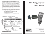
1
ADVANCED AND EVER ADVANCING MITSUBISHI ELECTRIC MITSUBISHI 16-BIT SINGLE-CHIP MICROCOMPUTER M16C FAMILY M16C/60 M16C/20 SERIES <Assembler language> Programming Manual MITSUBISHI ELECTRIC Keep safety first in your circuit designs! ● Mitsubishi Electric Corporation puts the maximum effort into making semiconductor products better and more reliable, but there is always the possibility that trouble may occur with them. Trouble with semiconductors may lead to personal injury, fire or property damage. Remember to give due consideration to safety when making your circuit designs, with appropriate measures such as (i) placement of substitutive, auxiliary circuits, (ii) use of non-flammable material or (iii) prevention against any malfunction or mishap. Notes regarding these materials ● ● ● ● ● ● ● ● These materials are intended as a reference to assist our customers in the selection of the Mitsubishi semiconductor product best suited to the customer's application; they do not convey any license under any intellectual property rights, or any other rights, belonging to Mitsubishi Electric Corporation or a third party. Mitsubishi Electric Corporation assumes no responsibility for any damage, or infringement of any third-party's rights, originating in the use of any product data, diagrams, charts, programs, algorithms, or circuit application examples contained in these materials. All information contained in these materials, including product data, diagrams, charts, programs and algorithms represents information on products at the time of publication of these materials, and are subject to change by Mitsubishi Electric Corporation without notice due to product improvements or other reasons. It is therefore recommended that customers contact Mitsubishi Electric Corporation or an authorized Mitsubishi Semiconductor product distributor for the latest product information before purchasing a product listed herein. The information described here may contain technical inaccuracies or typographical errors. Mitsubishi Electric Corporation assumes no responsibility for any damage, liability, or other loss rising from these inaccuracies or errors. Please also pay attention to information published by Mitsubishi Electric Corporation by various means, including the Mitsubishi Semiconductor home page (http:// www.mitsubishichips.com). When using any or all of the information contained in these materials, including product data, diagrams, charts, programs, and algorithms, please be sure to evaluate all information as a total system before making a final decision on the applicability of the information and products. Mitsubishi Electric Corporation assumes no responsibility for any damage, liability or other loss resulting from the information contained herein. Mitsubishi Electric Corporation semiconductors are not designed or manufactured for use in a device or system that is used under circumstances in which human life is potentially at stake. Please contact Mitsubishi Electric Corporation or an authorized Mitsubishi Semiconductor product distributor when considering the use of a product contained herein for any specific purposes, such as apparatus or systems for transportation, vehicular, medical, aerospace, nuclear, or undersea repeater use. The prior written approval of Mitsubishi Electric Corporation is necessary to reprint or reproduce in whole or in part these materials. If these products or technologies are subject to the Japanese export control restrictions, they must be exported under a license from the Japanese government and cannot be imported into a country other than the approved destination. Any diversion or reexport contrary to the export control laws and regulations of Japan and/or the country of destination is prohibited. Please contact Mitsubishi Electric Corporation or an authorized Mitsubishi Semicon ductor product distributor for further details on these materials or the products con tained therein. Preface This manual describes the basic knowledge of application program development for the M16C/60, M16C/20 series of Mitsubishi CMOS 16-bit microcomputers. The programming language used in this manual is the assembly language. If you are using the M16C/60, M16C/20 series for the first time, refer to Chapter 1, "Overview of M16C/60, M16C/20 Series". If you want to know the CPU architecture and instructions, refer to Chapter 2, "CPU Programming Model" or if you want to know the directive commands of the assembler, refer to Chapter 3, "Functions of Assembler". If you want to know practical techniques, refer to Chapter 4, "Programming Style". The instruction set of the M16C/60, M16C/20 series is detailed in "M16C/60, M16C/20 Series Software Manual". Refer to this manual when the knowledge of the instruction set is required. For information about the hardware of each type of microcomputer in the M16C/60, M16C/20 series, refer to the user's manual supplied with your microcomputer. For details about the development support tools, refer to the user's manual of each tool. Guide to Using This Manual This manual is an assembly language programming manual for the M16C/60, M16C/20 series. This manual can be used in common for all types of microcomputers built the M16C/60 series CPU core. This manual is written assuming that the reader has a basic knowledge of electrical circuits, logic circuits, and microcomputers. This manual consists of four chapters. The following provides a brief guide to the desired chapters and sections. • To see the overview and features of the M16C/60, M16C/20 series → Chapter 1 Overview of M16C/60, M16C/20 Series • To understand the address space, register structure, and addressing and other knowledge required for programming → Chapter 2 CPU Programming Model • To know the functions of instructions, the method for writing instructions, and the usable addressing modes → Chapter 2 CPU Programming Model, 2.6 Instruction Set • To know how to use interrupts → Chapter 2 CPU Programming Model, 2.7 Interrupts → Chapter 4 Programming Style, 4.3 Interrupts • To check the functions of and the method for writing directive commands → Chapter 3 Functions of Assembler, 3.2 Writing Source Program • To know the M16C/60, M16C/20 series' programming techniques → Chapter 4 Programming Style • To know the M16C/60, M16C/20 series' development procedures → Chapter 4 Programming Style, 4.7 Generating Object File M16C Family-related document list Usages (Microcomputer development flow) Type of document Outline design of system Hardware Selection of microcomputer Data sheet and data book User’s manual Hardware development Software development Software Detail design of system Contents Hardware specifications (pin assignment, memory map, specifications of peripheral functions, electrical characteristics, timing charts) Detailed description about hardware specifications, operation, and application examples (connection with peripherals, relationship with software) Programming manual Method for creating programs using assembly and C languages Software manual Detailed description about operation of each instruction (assembly language) System evaluation M16C Family Line-up M16C Family M16C/80 Series M16C/80 Group M16C/60 Series M16C/60 Group M16C/61 Group M16C/62 Group M16C/20 Series M16C/20 Group M16C/21 Group Table of contents Chapter 1 Overview of M16C/60, M16C/20 Series 1.1 Features of M16C/60, M16C/20 Series ..........................................................................................2 1.2 Outline of M16C/60, M16C/20 Group ........................................................................................... 3 1.3 Introduction to CPU Architecture .................................................................................................5 Chapter 2 CPU Programming Model 2.1 Address Space ............................................................................................................................. 10 2.1.1 Operation Modes and Memory Mapping ............................................................................... 10 2.1.2 SFR Area ...............................................................................................................................12 2.1.3 Fixed Vector Area.................................................................................................................. 15 2.2 Register Set ..................................................................................................................................16 2.3 Data Types ....................................................................................................................................21 2.4 Data Arrangement ........................................................................................................................23 2.5 Addressing Modes .......................................................................................................................24 2.5.1 2.5.2 2.5.3 2.5.4 2.5.5 Types of Addressing Modes .................................................................................................. 24 General Instruction Addressing ............................................................................................. 25 Special Instruction Addressing ...............................................................................................34 Bit Instruction Addressing ......................................................................................................39 Instruction Formats ................................................................................................................46 2.6 Instruction Set ............................................................................................................................. 47 2.6.1 2.6.2 2.6.3 2.6.4 Instruction List ........................................................................................................................48 Transfer and String Instructions .............................................................................................64 Arithmetic Instructions ........................................................................................................... 67 Sign Extend Instruction ......................................................................................................... 74 2.6.5 2.6.6 2.6.7 2.6.8 Bit Instructions .......................................................................................................................75 Branch Instructions ................................................................................................................77 High-level Language Support Instructions .............................................................................81 OS Support Instructions .........................................................................................................83 2.7 Outline of Interrupt ......................................................................................................................86 2.7.1 Interrupt Sources and Control ............................................................................................... 86 2.7.2 Interrupt Sequence ................................................................................................................87 Chapter 3 Functions of Assembler 3.1 Outline of AS30 System ...............................................................................................................90 3.2 Method for Writing Source Program ..........................................................................................93 3.2.1 3.2.2 3.2.3 3.2.4 3.2.5 Basic Rules ........................................................................................................................... 93 Address Control .................................................................................................................. 101 Directive Commands ........................................................................................................... 108 Macro Functions .................................................................................................................. 116 Structured Description Function .......................................................................................... 124 Chapter 4 Programming Style 4.1 Hardware Definition .................................................................................................................. 126 4.1.1 4.1.2 4.1.3 4.1.4 4.1.5 Defining SFR Area .............................................................................................................. Allocating RAM Data Area................................................................................................... Allocating ROM Data Area .................................................................................................. Defining a Section ............................................................................................................... Sample Program List 1 (Initial Setting 1) ............................................................................ 126 129 130 131 133 4.2 Initial Setting the CPU .............................................................................................................. 136 4.2.1 4.2.2 4.2.3 4.2.4 4.2.5 4.2.6 4.2.7 Setting CPU Internal Registers ........................................................................................... Setting Stack Pointer .......................................................................................................... Setting Base Registers (SB, FB) ......................................................................................... Setting Interrupt Table Register (INTB) ............................................................................... Setting Variable/Fixed Vector .............................................................................................. Setting Peripheral Functions ............................................................................................... Sample Program List 2 (Initial Setting 2) ............................................................................ 136 136 136 136 137 137 139 4.3 Setting Interrupts ...................................................................................................................... 142 4.3.1 4.3.2 4.3.3 4.3.4 4.3.5 4.3.6 4.3.7 4.3.8 Setting Interrupt Table Register .......................................................................................... Setting Variable/Fixed Vectors ............................................................................................ Enabling Interrupt Enable Flag ........................................................................................... Setting Interrupt Control Register ....................................................................................... Saving and Restoring Registers in Interrupt Handler Routine ............................................ Sample Program List 3 (Software Interrupt) ....................................................................... ISP and USP ....................................................................................................................... Multiple Interrupts ............................................................................................................... 142 143 144 144 145 147 150 153 4.4 Dividing Source File ................................................................................................................. 154 4.4.1 Concept of Sections ............................................................................................................ 154 4.4.2 Dividing Source File ............................................................................................................ 156 4.4.3 Library File .......................................................................................................................... 162 4.5 A Little Tips... ............................................................................................................................. 164 4.5.1 4.5.2 4.5.3 4.5.4 Stack Area........................................................................................................................... Setup Values of SB and FB Registers ................................................................................ Alignment Specification ....................................................................................................... Watchdog Timer .................................................................................................................. 164 166 167 169 4.6 Sample Programs ..................................................................................................................... 172 4.7 Generating Object Files ............................................................................................................ 174 4.7.1 Assembling.......................................................................................................................... 175 1 Chapter 1 Overview of M16C/60, M16C/20 Series 1.1 Features of M16C/60, M16C/20 Series 1.2 Outline of M16C/60, M16C/20 Group 1.3 Introduction to CPU Architecture 1 Overview of M16C/60, M16C/20 Series 1.1 Features of M16C/60, M16C/20 Series 1.1 Features of M16C/60, M16C/20 Series The M16C/60, M16C/20 series is a line of single-chip microcomputers that have been developed for use in built-in equipment. This section describes the features of the M16C/60, M16C/20 series. Features of the M16C/60, M16C/20 series The M16C/60, M16C/20 series has its frequently used instructions placed in a 1-byte op-code. For this reason, it allows you to write a highly memory efficient program. Furthermore, although the M16C/60, M16C/20 series is a 16-bit microcomputer, it can perform 1, 4, and 8-bit processing efficiently. The M16C/60, M16C/20 series has many instructions that can be executed in one clock period. For this reason, it is possible to write a high-speed processing program. The M16C/60, M16C/20 series provides 1 Mbytes of linear addressing space. Therefore, the M16C/60, M16C/20 series is also suitable for applications that require a large program size. The features of the M16C/60, M16C/20 series can be summarized as follows: (1) The M16C/60, M16C/20 series allows you to create a memory-efficient program without requiring a large memory capacity. (2) The M16C/60, M16C/20 series allows you to create a high- speed processing program. (3) The M16C/60, M16C/20 series provides 1 Mbytes of addressing space, making it suitable for even large-capacity applications. 1.2 Outline of M16C/60, M16C/20, M16C/20 Group This section explains the M16C/60 group as a typical internal structure of the M16C/60 series and M16C/20 group as a typical internal structure of the M16C/20 series. The M16C/60, M16C/20 group is a basic product of the M16C/60, M16C/20 series. For details about this product, refer to the data sheets and user's manuals. 2 Overview of M16C/60 Series 1 1.2 Outline of M16C/60 Group, M16C/20 Group Internal Block Diagram Figure 1.2.1 shows a block diagram of the M16C/60 group. (1) M16C/60 group 8 8 I/O ports Port P0 8 Port P1 8 Port P2 8 Port P3 Expandable up to 10 channels) System clock generator XIN-XOUT XCIN-XCOUT UART/clock synchronous SI/ O(8 bits X 2 channels ) M16C/60 series16-bit CPU core Registers DMAC ROM Vector table INTB RAM 10K bytes Multiplier (8 bits X 2 channels) SB Note : +1 UART/clock synchronous SI/O (In case of the M16C/61 group) +1 UART/clock synchronous SI/O, +1 clock asynchronous SI/O, +3 timer B (In case of the M16C/62 group) (2) M16C/20 group 8 I/O ports Port P0 8 6 Port P1 6 Port P3 8 5 Port P4 Port P5 Port P6 Internal peripheral functions A-D converter System clock generator Timer (10 bits X 8 channels XIN-XOUT XCIN-XCOUT Timer TA0 (16 bits) Timer TB0 (16 bits) Timer TB1 (16 bits) Timer TX0 (16 bits) Timer TX1 (16 bits) Timer TX2 (16 bits) Expandable up to 13 channels) (8 bits X 1 channel) UART (8 bits X 1 channel) Registers (15 bits) Port P7 UART/clock synchronous SI/O M16C/60 series16-bit CPU core Watchdog timer 2 R0H R0L R0H R0L R1H R1L R1H R1L R2 R2 R3 R3 A0 A0 A1 A1 FB FB Program counter PC Vector table INTB Stack pointer ISP USP SB FLG Note 1: ROM size depends on MCU type. Note 2: RAM size depends on MCU type. Figure 1.2.1 Block diagram of the M16C/60 group 3 AAAAAA AAAAAA AAAAAA AAAAAA AAAAA AAAAA AAAAA Memory ROM (Note 1) RAM (Note 2) Multiplier 8 Port P10 D-A converter ISP USP 8 R0H R0L R0H R0L R1H R1L R1H R1L R2 R2 R3 R3 A0 A0 A1A1 FBFB (2 channels) Memory Stack pointer Port P9 Watchdog timer(15 bits) Port P85 CRC arithmetic circuit (CCITT ) (Polynomial : X16+X12+X5+1) 7 Timer TA0 (16 bits) Timer TA1 (16 bits) Timer TA2 (16 bits) Timer TA3 (16 bits) Timer TA4 (16 bits) Timer TB0 (16 bits) Timer TB1 (16 bits) Timer TB2 (16 bits) Port P6 8 (10 bits X 8 channels Port P5 Port P8 A-D converter Timer Port P4 Port P7 Internal peripheral functions 8 8 Overview of M16C/60 Series 1 1.2 Outline of M16C/60 Group, M16C/20 Group Outline Specifications of the M16C/60 Group Table 1.2.1 lists the outline specifications of the M16C/60 group. Table 1.2.1 Outline Specifications of M16C/60 Group Item Content Supply voltage 2.7 to 5.5 V (with 7 MHz external oscillator, 1 wait state) Package 100-pin plastic molded QFP Operating frequency 10 MHz (with 10 MHz external oscillator) Shortest instruction execution time 100 ns (with 10 MHz external oscillator) Basic bus cycle Internal memory : 100 ns (with 10 MHz external oscillator) External memory: 100 ns (with 10 MHz external oscillator, no wait state) Internal memory ROM capacity (Note) 64 Kbytes RAM capacity 10 Kbytes Operation mode Single-chip, memory expansion, and microprocessor modes External address space 1 Mbytes (linear)/64 Kbytes Address bus: 20 bits/16 bits External data bus width 8 bits/16 bits Bus specification Separate bus/multiplexed bus (4 chip select lines built-in) Clock generating circuit 2 circuits built-in (external ceramic or crystal resonator) Built-in peripheral functions Interrupt 17 internal sources, 5 external sources, 4 software sources; 7 levels (including key input interrupt) Multifunction 16-bit timer 5 timer A + 3 timer B Serial I/O 2 channels (asynchronous/synchronous switchable) A-D converter 10 bits, 8 + 2 channel input (10/8 bits switchable) D-A converter 8 bits, 2 channel output DMAC 2 channels (trigger: 15 factors) CRC calculation circuit 1 circuit built-in Watchdog timer 15-bit counter Programmable input/output 87 lines Input port 1 line (shared with P85 and NMI pin) Note: This does not include the M30600SFP, an external ROM version. 4 Overview of M16C/60 Series 1 1.2 Outline of M16C/60 Group, M16C/20 Group Outline Specifications of the M16C/20 Group Table 1.2.2 lists the outline specifications of the M16C/20 group. Table 1.2.2 Outline Specifications of M16C/20 Group Item Content Supply voltage 2.7 to 5.5 V (with 7 MHz external oscillator, 1 wait state) Package 52-pin plastic molded SDIP 56-pin plastic molded QFP Operating frequency 10 MHz (with 10 MHz external oscillator) Shortest instruction execution time 100 ns (with 10 MHz external oscillator) Basic bus cycle Internal memory : 100 ns (with 10 MHz external oscillator) Internal memory ROM capacity RAM capacity 1024bytes 32 Kbytes Operation mode Single-chip mode Clock generating circuit 2 circuits built-in (external ceramic or crystal resonator) Built-in peripheral functions Interrupt 9 internal sources, 3 external sources, 4 software sources; 7 levels (including key input interrupt) Multifunction 16-bit timer 1 timer A + 2 timer B + 3 timer X Serial I/O 2 channels (one is clock asynchronous/synchronous switchable, the other is clock asynchronous) A-D converter 10 bits, 8 + 2 channel input (10/8 bits switchable) Programmable input/output 43 lines 5 Overview of M16C/60, M16C/20 Series 1 1.3 Introduction to CPU Architecture 1.3 Introduction to CPU Architecture This section explains the CPU architecture of the M16C/60, M16C/20 series. Each item explained here is detailed in Chapter 2 of this manual. Register Structure Table 1.3.1 shows the register structure of the M16C/60, M16C/20 series. Seven registers--R0, R1, R2, R3, A0, A1, and FB--are available in two sets each. These sets are switched over by a register bank select flag. Table 1.3.1 Register Structure of M16C/60, M16C/20 Series Item Content Register structure Data registers Address registers Base registers AAAA AAAA AAAA AAAA AAAA AAAA AAAA AAAAAA AAAAAA AAAAAA AAAAAA AAAAAA 16 bits x 4 R0 R1 R2 R3 (32 bits x 2) 16 bits x 2 A0 A1 (32 bits x 1) 16 bits x 2 R2R0 R3R1 A1A0 AA AA AA AAAA AA (8 bits x 4) R2 R0 R0 R3 R1 R1 A1 A0 R0H R0L R1H R1L SB FB Control registers 20 bits x 2 PC INTB 16 bits x 3 USP ISP FLG b15 (Details of FLG) IPL b0 U I O B S Z D C : (PC) IPL : Processor interrupt priority level (Levels 0 to 7; larger the number, higher the priority) (PC) : Saves 4 high-order bits of PC when interrupt occurs. U : Stack pointer select flag (ISP when U = 0, USP when U = 1) I : Interrupt enable flag (Enabled when I = 1) O : Overflow flag (0 = 1 when overflow occurs) B : Register bank select flag (Register bank 0 when B = 0, register bank 1 when B = 1) S : Sign flag (S = 1 when operation resulted in negative, S = 0 when positive) Z : Zero flag (Z = 1 when operation resulted in zero) D : Debug flag (Program is single-stepped when D = 1) C : Carry flag (carry or borrow) 6 Overview of M16C/60, M16C/20 Series 1 1.3 Introduction to CPU Architecture Addressing Modes There are three types of addressing modes. (1) General instruction addressing .. A 64-Kbyte area (00000H to 0FFFFH) is accessed. (2) Special instruction addressing ... A 1-Mbyte area (00000H to FFFFFH) is accessed. (3) Bit instruction addressing ........... A 64-Kbyte area (00000H to 0FFFFH) is accessed in units of bits. Table 1.3.2 lists the M16C/60, M16C/20 series addressing modes that can be used in each type of addressing described above. Table 1.3.2 Addressing Modes of M16C/60, M16C/20 Series Item Content Addressing mode General instruction Special instruction Bit instruction Immediate O #imm: 8/16 bits x x Register direct O Data and address registers only O R2R0 or R3R1 or A1A0 * SHL, SHA, JMPI, and JSRI instructions only O R0, R1, R2, R3, A0, and A1 only Absolute O abs: 16 bits (0 to FFFFH) O abs: 20 bits (0 to FFFFFH) * LDE, STE, JMP, and JSR instructions only O bit,base: 16 bits (0 to 1FFFH) Address register indirect O [A0] or [A1] without dsp O [A1A0] without dsp * LDE and STE instructions only O [A0] or [A1] without dsp (0 to 1FFFH) Address register relative O [A0] or [A1] dsp: 8/16 bits O [A0] dsp: 20 bits only * LDE, STE, JMPI, and JSRI instructions only O [A0] or [A1] dsp: 8/16 bits SB relative and FB relative O [SB]dsp : 8/16bit (0 to 255 / 0 to 65534) O [FB]dsp : 8bit(-128 to +127) x O [SB] dsp: 8/11/16 bits (0 to 31/0 to 255/0 to 8191) O [FB]dsp : 8bit (-16 to +15) x O [SP] dsp: 8 bits (-128 to +127) * MOV instruction only x Program counter relative x O label .S: +2 to +9 .B: -128 to +127 .W: -32768 to +32767 * JMP and JSR instructions only x Control register direct x O INTBL, INTBH, ISP, USP, SB, FB, FLG * LDC, STC, PUSHC, and POPC instructions only x FLG direct x x O Stack pointer relative 7 U, I, O, B, S, Z, D, and C flags * FCLR and FSET instructions only Overview of M16C/60, M16C/20 Series 1 1.3 Introduction to CPU Architecture Instruction Set Table 1.3.3 lists the instructions of the M16C/60, M16C/20 series classified by function. There is a total of 91 discrete instructions. Table 1.3.3 Instruction Set of M16C/60, M16C/20 Series Item Instruction set Data transfer instructions 14 instructions Arithmetic/logic instructions 31 instructions Content 8-bit variable length: 91 instructions • Transfer instructions • Push/pop instructions • Extended data area transfer instructions • 4-bit transfer instructions • Exchange between register and register/ memory instruction • Conditional transfer instructions MOV, MOVA PUSH, PUSHM, PUSHA / POP, POPM LDE, STE MOVDir XCHG • Add instructions • Subtract instructions • Multiply instructions • Divide instructions • Decimal add instructions • Decimal subtract instructions • Increment/decrement instructions • Sum of products instruction • Compare instruction • Others (absolute value, 2's complement, sign extension) • Logic instructions • Test instruction • Shift/rotate instructions ADD, ADC, ADCF SUB, SBB MUL, MULU DIV, DIVU, DIVX DADD, DADC DSUB, DSBB INC / DEC RMPA CMP ABS, NEG, EXTS AND, OR, XOR, NOT STZ, STNZ, STZX TST SHL, SHA / ROT, RORC, ROLC Branch instructions • Unconditional branch instruction 10 instructions • Conditional branch instruction • Indirect jump instruction • Special page branch instruction • Subroutine call instruction • Indirect subroutine call instruction • Special page subroutine call instruction • Subroutine return instruction • Add (subtract) and conditional branch instructions JMP JCnd JMPI JMPS JSR JSRI JSRS RTS ADJNZ, SBJNZ Bit manipulate instructions 14 instructions BCLR, BSET, BNOT, BTST, BNTST, BAND, BNAND, BOR, BNOR, BXOR, BNXOR, BMCnd, BTSTS, BTSTC String instructions 3 instructions SMOVF, SMOVB, SSTR Other instructions 19 instructions • Control register manipulate instructions • Flag register manipulate instructions • OS support instructions • High-level language support instructions • Debugger support instruction • Interrupt-related instructions • External interrupt wait instruction • No-operation instruction 8 LDC, STC, LDINTB, LDIPL, PUSHC, POPC FSET, FCLR LDCTX, STCTX ENTER, EXITD BRK REIT, INT, INTO, UND WAIT NOP 2 Chapter 2 CPU Programming Model 2.1 2.2 2.3 2.4 2.5 2.6 2.7 Address Space Register Sets Data Types Data Arrangement Addressing Modes Instruction Set Outline of Interrupt CPU Programming Model 2 2.1 Address Space 2.1 Address Space The M16C/60,M16C/20 series has 1 Mbytes of address space ranging from address 00000H to address FFFFFH. This section explains the address space and memory mapping, the SFR area, and the fixed vector area of the M16C/60 group. 2.1.1 Operation Modes and Memory Mapping The M16C/60 group chooses one operation mode from three modes available: single-chip, memory expansion, and microprocessor modes. The M16C/60 group address space and the usable areas and memory mapping varies with each operation mode. Address Space Figure 2.1.1 shows the address space of the M16C/60 group. Addresses 00000H to 003FFH are the Special Function Register (SFR) area. The SFR area in each type of M16C/60 group microcomputer begins with address 003FFH and expands toward smaller addresses. Addresses following 00400H constitute the memory area. The memory area in each type of M16C/ 60 group microcomputer consists of a RAM area which begins with address 00400H and expands toward larger addresses and a ROM area which begins with address FFFFFH and expands toward smaller addresses. However, addresses FFE00H to FFFFFH are the fixed vector area. 00000H 003FFH 00400H Direction in which SFR area expands SFR area Direction in which internal RAM expands Internal RAM area 0FFFFH 10000H External memory area Internal ROM area FFE00H FFFFFH Direction in which internal ROM expands Fixed vector area Figure 2.1.1 Address space 10 CPU Programming Model 2 2.1 Address Space Operation Modes and Memory Mapping • Single-chip mode In this mode, only the internal areas (SFR, internal RAM, and internal ROM) can be accessed. • Memory expansion mode In this mode, the internal areas (SFR, internal RAM, and internal ROM) and an external memory area can be accessed. • Microprocessor mode In this mode, the SFR and internal RAM areas and an external memory area can be accessed. (The internal ROM area cannot be accessed.) Figure 2.1.2 shows the M16C/60 group memory mapping in each operation mode. AA AA Internal area External area (using external memory chips) Cannot be used. (ROM: 64 Kbytes; RAM: 10 Kbytes) 00000H SFR area SFR area SFR area Internal RAM area Internal RAM area Internal RAM area 00400H 02C00H AAAAA AAAAA AAAAA AAAAA AAAAA AAAAA AAAAAAAAAA AAAAA AAAAA AAAAA AAAAA AAAAA Internal reserved area Cannot be used External memory area Internal reserved area F0000H Internal ROM area FFFFFH Single-chip mode Internal reserved area External memory area Internal ROM area Memory expansion mode Figure 2.1.2 Operation modes and memory mapping 11 Microprocessor mode CPU Programming Model 2 2.1 Address Space 2.1.2 SFR Area A range of control registers are allocated in this area, including the processor mode register that determines the operation mode and the peripheral unit control registers for I/O ports, A-D converter, UART, and timers. For the bit configurations of these control registers, refer to the M16C/60 group data sheets and user's manuals. The unused locations in the SFR area are reserved for the system and cannot be used by the user. SFR Area: Control Register Allocation Figures 2.1.3 and 2.1.4 show control register allocations in the SFR area. 000016 004016 000116 004116 000216 004216 004316 000316 000416 000516 000616 000716 000816 000916 000A16 004416 Processor mode register 0 (PM0) Processor mode register 1(PM1) System clock control register 0 (CM0) System clock control register 1 (CM1) Chip select control register (CSR) Address match interrupt enable register (AIER) Protect register (PRCR) 004516 004616 004716 004816 004916 004A16 000B16 004B16 000C16 004C16 000D16 004D16 000E16 000F16 004E16 Watchdog timer start register (WDTS) Watchdog timer control register (WDC) 004F16 005016 001016 001116 005116 Address match interrupt register 0 (RMAD0) 001216 005216 001316 005316 005416 001416 001516 005516 Address match interrupt register 1 (RMAD1) 001616 005616 001716 005716 001816 005816 001916 005916 001A16 005A16 001B16 005B16 001C16 005C16 001D16 005D16 001E16 005E16 001F16 005F16 002016 002116 DMA0 source pointer (SAR0) 002216 002316 002416 002516 DMA0 destination pointer (DAR0) 002616 002716 002816 002916 DMA0 transfer counter (TCR0) 002A16 002B16 002C16 DMA0 control register (DM0CON) 002D16 002E16 002F16 003016 003116 DMA1 source pointer (SAR1) 003216 003316 003416 003516 DMA1 destination pointer (DAR1) 003616 003716 003816 003916 DMA1 transfer counter (TCR1) 003A16 003B16 003C16 DMA0 interrupt control register (DM0IC) DMA1 interrupt control register (DM1IC) Key input interrupt control register (KUPIC) A-D conversion interrupt control register (ADIC) DMA1 control register (DM1CON) 003D16 003E16 003F16 Figure 2.1.3 Control register allocation 1 12 UART0 transmit interrupt control register (S0TIC) UART0 receive interrupt control register (S0RIC) UART1 transmit interrupt control register (S1TIC) UART1 receive interrupt control register (S1RIC) Timer A0 interrupt control register (TA0IC) Timer A1 interrupt control register (TA1IC) Timer A2 interrupt control register (TA2IC) Timer A3 interrupt control register (TA3IC) Timer A4 interrupt control register (TA4IC) Timer B0 interrupt control register (TB0IC) Timer B1 interrupt control register (TB1IC) Timer B2 interrupt control register (TB2IC) INT0 interrupt control register (INT0IC) INT1 interrupt control register (INT1IC) INT2 interrupt control register (INT2IC) CPU Programming Model 2 2.1 Address Space 038016 038116 038216 038316 038416 Count start flag (TABSR) Clock prescaler reset flag (CPSRF) One-shot start flag (ONSF) Trigger select register (TRGSR) Up-down flag (UDF) 03C016 03C116 03C216 03C316 03C416 038516 03C516 038616 03C616 038716 038816 038916 038A16 038B16 038C16 038D16 038E16 038F16 039016 039116 039216 039316 039416 039516 039616 039716 039816 039916 039A16 039B16 039C16 039D16 Timer A0 (TA0) Timer A1 (TA1) Timer A2 (TA2) Timer A3 (TA3) Timer A4 (TA4) Timer B0 (TB0) Timer B1 (TB1) Timer B2 (TB2) Timer A0 mode register (TA0MR) Timer A1 mode register (TA1MR) Timer A2 mode register (TA2MR) Timer A3 mode register (TA3MR) Timer A4 mode register (TA4MR) Timer B0 mode register (TB0MR) Timer B1 mode register (TB1MR) Timer B2 mode register (TB2MR) 039E16 03C716 03C816 03C916 03CA16 03CB16 03CC16 03CD16 03CE16 03CF16 03D416 03D616 03D716 03D816 03DA16 03DC16 UART0 transmit buffer register (U0TB) UART0 transmit/receive control register 0 (U0C0) UART0 transmit/receive control register 1 (U0C1) UART0 receive buffer register (U0RB) 03E216 03E316 03E416 03E516 03E616 03E716 03E816 UART1 bit rate generator (U1BRG) 03E916 03AE16 UART1 transmit buffer register (U1TB) UART1 transmit/receive control register 0 (U1C0) UART1 transmit/receive control register 1 (U1C1) 03AF16 UART1 receive buffer register (U1RB) 03B016 UART transmit/receive control register 2 (UCON) 03EA16 03EB16 03EC16 03ED16 03EE16 03EF16 03F016 03B116 03F116 03B216 03F216 03B316 03F316 03B416 03F416 03B516 03F516 03B616 03F616 03B716 03F716 03B816 03F816 DMA0 cause select register (DM0SL) DMA1 cause select register (DM1SL) 03BD16 03BE16 Port P0 (P0) Port P1 (P1) Port P0 direction register (PD0) Port P1 direction register (PD1) Port P2 (P2) Port P3 (P3) Port P2 direction register (PD2) Port P3 direction register (PD3) Port P4 (P4) Port P5 (P5) Port P4 direction register (PD4) Port P5 direction register (PD5) Port P6 (P6) Port P7 (P7) Port P6 direction register (PD6) Port P7 direction register (PD7) Port P8 (P8) Port P9 (P9) Port P8 direction register (PD8) Port P9 direction register (PD9) Port P10 (P10) Port P10 direction register (PD10) 03FA16 03FB16 03BB16 03BC16 D-A control register (DACON) 03F916 03B916 03BA16 D-A register 1 (DA1) 03DF16 03A916 03AD16 A-D control register 0 (ADCON0) A-D control register 1 (ADCON1) D-A register 0 (DA0) 03DD16 UART1 transmit/receive mode register (U1MR) 03AC16 A-D control register 2 (ADCON2) 03DB16 03A816 03AB16 A-D register 7 (AD7) 03D916 03E116 03AA16 A-D register 6 (AD6) 03D516 03E016 03A716 A-D register 5 (AD5) 03D316 UART0 bit rate generator (U0BRG) 03A616 A-D register 4 (AD4) 03D216 03A116 03A516 A-D register 3 (AD3) 03D116 UART0 transmit/receive mode register (U0MR) 03A416 A-D register 2 (AD2) 03DE16 039F16 03A316 A-D register 1 (AD1) 03D016 03A016 03A216 A-D register 0 (AD0) CRC data register (CRCD) CRC input register (CRCIN) 03BF16 03FC16 03FD16 03FE16 03FF16 Figure 2.1.4 Control register allocation 2 13 Pull-up control register 0 (PUR0) Pull-up control register 1 (PUR1) Pull-up control register 2 (PUR2) CPU Programming Model 2 2.1 Address Space Determination of Operation Mode The M16C/60 group operation mode is determined by bits 0 and 1 of the processor mode register 0 (address 00004H). Figure 2.1.5 shows the configuration of processor mode register 0. Processor mode register 0 (Note 1) b7 b6 b5 b4 b3 b2 b1 b0 Symbol PM0 Address 000416 When reset 0016 (Note 2) Bit name Bit symbol Function Processor mode bit b1 b0 PM02 R/W mode select bit 0 : RD,BHE,WR 1 : RD,WRH,WRL PM03 Software reset bit PM04 Multiplexed bus space select bit PM00 PM01 PM05 0 0: Single-chip mode 0 1: Memory expansion mode 1 0: Inhibited 1 1: Microprocessor mode AA A A AA A A A AA A AA AA A A A AA A AA RW The device is reset when this bit is set to “1”. The value of this bit is “0” when read. b5 b4 0 0 : Multiplexed bus is not used 0 1 : Allocated to CS2 space 1 0 : Allocated to CS1 space 1 1 : Allocated to entire space (Note 4) PM06 Port P40 to P43 function select bit (Note 3) 0 : Address output 1 : Port function (Address is not output) PM07 BCLK output disable bit 0 : BCLK is output 1 : BCLK is not output (Pin is left floating) Note 1: Set bit 1 of the protect register (address 000A16) to “1” when writing new values to this register. Note 2: If the VCC voltage is applied to the CNVSS, the value of this register when reset is 0316. (PM00 and PM01 are both set to “1”.) Note 3: Valid in microprocessor and memory expansion modes. Note 4: In microprocessor mode, multiplexed bus for the entire space cannot be selected. In memory expansion mode, when multiplexed bus for the entire space is selected, address bus range is 256 bytes in each chip select. Figure 2.1.5 Processor mode register 0 14 CPU Programming Model 2 2.1 Address Space 2.1.3 Fixed Vector Area The M16C/60 group fixed vector area consists of addresses FFE00H to FFFFFH. Addresses FFE00H to FFFDBH in this area constitute a special page vector table. This table is used to store the start addresses of subroutines and jump addresses, so that subroutine call and jump instructions can be executed using two bytes, helping to reduce the number of program steps. Addresses FFFDCH to FFFFFH in the fixed vector area constitute a fixed interrupt vector table for reset and NMI. This table is used to store the start addresses of interrupt routines. An interrupt vector table for timer interrupts, etc. can be set at any desired address by an internal register (INTB). For details, refer to the section dealing with interrupts in Chapter 4. Memory Mapping in Fixed Vector Area Figure 2.1.6 shows memory mapping for the special page vector table and fixed vector area. 255 FFE02H 254 ○ ○ ○ Special page vector table ○ ○ FFE00H FFFDBH FFFDCH 18 Special page number FFFDCH Interrupt vector table FFFFFH FFFE0H Undefined instruction Overflow (INTO instruction) FFFE4H BRK instruction FFFE8H Address match FFFECH Single step FFFF0H Watchdog timer FFFF4H DBC FFFF8H NMI FFFFCH Reset Figure 2.1.6 Memory mapping in fixed vector area 15 CPU Programming Model 2 2.2 Register Set 2.2 Register Set This section describes the general-purpose and control registers of the M16C/60 series CPU core. Register Structure Figure 2.2.1 shows the register structure of the M16C/60 series CPU core. Seven registers--R0, R1, R2, R3, A0, A1, and FB--are available in two sets each. The following shows the function of each register. General-purpose registers (1) Data registers (R0, R1, R2, R3) These registers consist of 16 bits each and are used mainly for data transfer and arithmetic/ logic operations. Registers R0 and R1 can be used separately for upper bytes (R0H, R1H) and lower bytes (R0L, R1L) as 8-bit data registers. For some instructions, registers R2 and R0 and registers R3 and R1 can be combined for use as 32-bit data registers (R2R0, R3R1), respectively. (2) Address registers (A0, A1) These registers consist of 16 bits, and have the functions equivalent to those of the data registers. In addition, these registers are used in address register indirect addressing and address register relative addressing. For some instructions, registers A1 and A0 can be combined for use as a 32-bit address register (A1A0). (3) Frame base register (FB) This register consists of 16 bits, and is used in FB relative addressing. (4) Static base register (SB) This register consists of 16 bits, and is used in SB relative addressing. Control registers (5) Program counter (PC) This counter consists of 20 bits, indicating the address of an instruction to be executed. (6) Interrupt table register (INTB) This register consists of 20 bits, indicating the start address of an interrupt vector table. (7) Stack pointers (USP, ISP) There are two stack pointers: a user stack pointer (USP) and an interrupt stack pointer (ISP). Both of these pointers consist of 16 bits. The stack pointers used (USP or ISP) are switched over by a stack pointer select flag (U flag). The U flag is assigned to bit 7 of the flag register (FLG). (8) Flag register (FLG) This register consists of 11 bits, each of which is used as a flag. 16 CPU Programming Model 2 2.2 Register Set Data registers 8 bits 8 bits R0 R0H R0L R1 R1H R1L Register bank 0 Register bank 1 20 bits PC Program counter 4 bits R2 INTB INTBH 16 bits INTBL Interrupt table register R3 16 bits Address registers USP 16 bits User stack pointer A0 ISP Interrupt stack pointer A1 SB Static base register FLG Frame base register 16 bits FB Figure 2.2.1 Register structure 17 Flag register CPU Programming Model 2 2.2 Register Set Flag Register (FLG) Figure 2.2.2 shows the bit configuration of the flag register (FLG). The function of each flag is described below. • Bit 0: Carry flag (C flag) This bit holds a carry or borrow that has occurred in an arithmetic/logic operation or a bit that has been shifted out. • Bit 1: Debug flag (D flag) This flag enables a single-step interrupt. When this flag is 1, a single-step interrupt is generated after instruction execution. When the interrupt is accepted, this flag is cleared to 0. • Bit 2: Zero flag (Z flag) This flag is set to 1 when the operation resulted in 0; otherwise, the flag is 0. • Bit 3: Sign flag (S flag) This flag is set to 1 when the operation resulted in an negative number. The flag is 0 when the result is positive. • Bit 4: Register bank specifying flag (B flag) This flag chooses a register bank. Register bank 0 is selected when the flag is 0. Register bank 1 is selected when the flag is 1. • Bit 5: Overflow flag (O flag) This flag is set to 1 when the operation resulted in an overflow. • Bit 6: Interrupt enable flag (I flag) This flag enables a maskable interrupt. The interrupt is enabled when the flag is 1, and is disabled when the flag is 0. This flag is cleared to 0 when the interrupt is accepted. • Bit 7: Stack pointer specifying flag (U flag) The user stack pointer (USP) is selected when this flag is 1. The interrupt stack pointer (ISP) is selected when the flag is 0. This flag is cleared to 0 when a hardware interrupt is accepted or an INT instruction of software interrupt numbers 0 to 31 is executed. • Bits 8 to 11: Reserved. • Bits 12 to 14: Processor interrupt priority level (IPL) The processor interrupt priority level (IPL) consists of three bits, specifying the IPL in eight levels from level 0 to level 7. If the priority level of a requested interrupt is greater than the IPL, the interrupt is enabled. • Bit 15: Reserved. 18 CPU Programming Model 2 2.2 Register Set AAAAAAAAAAAA AAA AA AAA b15 b0 IPL U I O B S Z D C Flag Register (FLG) Carry flag Debug flag Zero flag Sign flag Register bank select flag Overflow flag Interrupt enable flag Stack pointer select flag Reserved area Processor interrupt priority level Reserved area Figure 2.2.2 Bit configuration of flag register (FLG) 19 CPU Programming Model 2 2.2 Register Set Register Status after Reset is Cleared Table 2.2.1 lists the status of each register after a reset is cleared. (See Note below.) Table 2.2.1 Register Status after Reset Cleared Register Name Status after Reset is Cleared Data registers (R0, R1, R2, R3) 0000H Address registers (A0, A1) 0000H Frame base register (FB) 0000H Interrupt table register (INTB) 00000H User stack pointer (USP) 0000H Interrupt stack pointer (ISP) 0000H Static base register (SB) 0000H Flag register (FLG) 0000H Note: For the control register status in the SFR area after a reset is cleared, refer to the M16C/60 group data sheets and user's manuals. 20 CPU Programming Model 2 2.3 Data Types 2.3 Data Types There are four data types handled by the M16C/60, M16C/20 series: integer, decimal (BCD), string, and bit. This section describes these data types. Integer An integer may be a signed or an unsigned integer. A negative value of a signed integer is represented by a 2's complement. b7 Signed byte (8-bit) integer b0 S b7 b0 Unsigned byte (8-bit) integer b15 b0 S Signed word (16-bit) integer b15 b0 Unsigned word (16-bit) integer b31 Signed long word (32-bit) integer b0 S b31 b0 Unsigned long word (32-bit) integer S: Sign bit Figure 2.3.1 Integer data Decimal (BCD) The BCD code is handled in packed format. This type of data can be used in four kinds of decimal arithmetic instructions: DADC, DADD, DSBB, and DSUB. b7 b0 1-byte packed format (2 digits) b15 2-byte packed format (4 digits) Figure 2.3.2 Decimal data 21 b0 CPU Programming Model 2 2.3 Data Types String A string is a block of data comprised of a consecutive number of 1-byte or 1-word (16-bit) data. This type of data can be used in three kinds of string instructions: SMOVB, SMOVF, and SSTR. • String of byte (8-bit) data 8 ··· ··· • String of word (16-bit) data 16 ··· ··· Figure 2.3.3 String data Bit Bit can be used in 14 kinds of bit instructions, including BCLR, BSET, BTST, and BNTST. Bits in each register are specified by a register name and a bit number, 0 to 15. Memory bits are specified by a different method in a different range depending on the addressing mode used. For details, refer to Section 2.5.4, "Bit Instruction Addressing". b15 b0 b15 b0 → 2,R0 (R0 register, bit 2) R0 → 14,A0 (A0 register, bit 14) A0 Figure 2.3.4 Specification of register bits Address b7 b0 00000H (n – 1)H nH (n +1)H n+1 Memory map b7 n b0 b7 n–1 b0 b7 0 b0 b7 b0 → 2,nH (Address nH, bit 2) Bit map base Figure 2.3.5 Specification of memory bits 22 CPU Programming Model 2 2.4 Data Arrangement 2.4 Data Arrangement The M16C/60, M16C/20 series can handle nibble (4-bit) and byte (8-bit) data efficiently. This section explains the data arrangements that can be handled by the M16C/60, M16C/20 series. Data Arrangement in Register Figure 2.4.1 shows the relationship between the data sizes and the bit numbers of a register. As shown below, the bit number of the least significant bit (LSB) is 0. The bit number of the most significant bit (MSB) varies with the data sizes handled. b3 b0 Nibble (4 bits) b7 b0 Byte (8 bits) b15 b0 Word (16 bits) b31 b0 Long word (32 bits) MSB LSB Figure 2.4.1 Data arrangement in register Data Arrangement in Memory Figure 2.4.2 shows the data arrangement in the M16C/60, M16C/20 series memory. Data is arranged in memory in units of 8 bits as shown below. A word (16 bits) is divided between the lower byte and the upper byte, with the lower byte, DATA(L), placed in a smaller address location. Similarly, addresses (20 bits) and long words (32 bits) are located in memory beginning with the lower byte, DATA(L) or DATA(LL). b7 N b0 b7 b0 b7 b0 b7 b0 N DATA(L) N DATA(L) N DATA(LL) N+1 N+1 DATA(H) N+1 DATA(M) N+1 DATA(LH) N+2 N+2 N+2 DATA(H) N+2 DATA(HL) N+3 N+3 N+3 N+3 DATA(HH) DATA Byte (8 bits) Word (16 bits) Address (20 bits) Figure 2.4.2 Data arrangement in memory 23 Long word (32 bits) CPU Programming Model 2 2.5 Addressing Modes 2.5 Addressing Modes This section explains the M16C/60, M16C/20 series addressing. 2.5.1 Types of Addressing Modes The three types of addressing modes shown below are available. (1) General instruction addressing .... An area from address 00000H to 0FFFFH is accessed. (2) Special instruction addressing ..... The entire address area from 00000H to FFFFFH is accessed. (3) Bit instruction addressing ............. An area from address 00000H to 0FFFFH is accessed in units of bits. This addressing mode is used in bit instructions. List of Addressing Modes All addressing modes are summarized in Table 2.5.1 below. Table 2.5.1 Addressing Modes of M16C/60, M16C/20 Series Item Content Addressing mode General instruction Special instruction Bit instruction Immediate O #imm: 8/16 bits x x Register direct O Data and address registers only O R2R0 or R3R1 or A1A0 * SHL, SHA, JMPI, and JSRI instructions only O R0, R1, R2, R3, A0, and A1 only Absolute O abs: 16 bits (0 to FFFFH) O abs: 20 bits (0 to FFFFFH) * LDE, STE, JMP, and JSR instructions only O bit,base: 16 bits (0 to 1FFFH) Address register indirect O [A0] or [A1] without dsp O [A1A0] without dsp * LDE and STE instructions only O [A0] or [A1] without dsp (0 to 1FFFH) Address register relative O [A0] or [A1] dsp: 8/16 bits O [A0] dsp: 20 bits only * LDE, STE, JMPI, and JSRI instructions only O [A0] or [A1] dsp: 8/16 bits SB relative and FB relative O [SB]dsp : 8/16bit (0 to 255 / 0 to 65534) O [FB]dsp : 8bit(-128 to +127) x O [SB] dsp: 8/11/16 bits (0 to 31/0 to 255/0 to 8191) O [FB]dsp : 8bit (-16 to +15) Stack pointer relative x O [SP] dsp: 8 bits (-128 to +127) * MOV instruction only x Program counter relative x O label .S: +2 to +9 .B: -128 to +127 .W: -32768 to +32767 * JMP and JSR instructions only x Control register direct x O INTBL, INTBH, ISP, USP, SB, FB, FLG * LDC, STC, PUSHC, and POPC instructions only x FLG direct x x O 24 U, I, O, B, S, Z, D, and C flags * FCLR and FSET instructions only CPU Programming Model 2 2.5 Addressing Modes 2.5.2 General Instruction Addressing This section explains each addressing in the general instruction addressing mode. Immediate The immediate indicated by #IMM is the subject on which operation is performed. Add a # before the immediate. Symbol: #IMM, #IMM8, #IMM16, #IMM20 Example: #123 (decimal) #7DH (hexadecimal) #01111011B (binary) Absolute The value indicated by abs16 is the effective address on which operation is performed. The range of effective addresses is 00000H to 0FFFFH. Symbol: abs16 Example: 8000H DATA (label) 00000H AAAA DATA:8000H Range of effective addresses 08000H 0FFFFH 10000H FFFFFH Figure 2.5.1 Absolute addressing Register direct A specified register is the subject on which operation is performed. However, only the data and address registers can be used here. Symbol: 8 bits R0L, R0H, R1L, R1H 16 bits R0, R1, R2, R3, A0, A1 25 CPU Programming Model 2 2.5 Addressing Modes Address Register Indirect The value of an address register is the effective address to be operated on. The range of effective addresses is 00000H to 0FFFFH. Symbol: [A0], [A1] Example: MOV.B #12H, [A0] b7 b0 00000H 01FFFH A Specifiable address range (0 to 01FFFH) FFFFFH Figure 2.5.2 Address register indirect addressing 26 CPU Programming Model 2 2.5 Addressing Modes Address Register Relative The value of an address register plus a displacement (dsp)(Note) is the effective address to be operated on. The range of effective addresses is 00000H to 0FFFFH. If the addition result exceeds 0FFFFH, the most significant bits above and including bit 17 are ignored. Symbol: dsp:8[A0], dsp:16[A0], dsp:8[A1], dsp:16[A1] (1) When dsp is handled as a displacement Example: MOV.B #34H,5[A0] 00000H 01000H A0 1000H +5 = Relative address range (0 to FFFFH) 01005H 34H 01005H 0FFFFH FFFFFH Figure 2.5.3 Address register relative addressing 1 (2) When address register (A0) is handled as a displacement Example: MOV.B #56H,1234H[A0] 00000H 01234H 1234H + A0 0005H Relative address range (0 to FFFFH) = 01239H 56H 01239H 0FFFFH FFFFFH Figure 2.5.4 Address register relative addressing 2 (3) When the addition result exceeds 0FFFFH Example: MOV.B #56H,1234H[A0] 00000H 01234H 1234H + A0 FFFFH Relative address range (0 to FFFFH) = 11238H 01238H Ignored 56H 0FFFFH FFFFFH Figure 2.5.5 Address register relative addressing 3 Note: The displacement (dsp) refers to a displacement from the reference address. In this manual, 8-bit dsp is expressed as dsp:8, and 16bit dsp is expressed as dsp:16. 27 CPU Programming Model 2 2.5 Addressing Modes SB Relative The value of the SB register plus dsp is the effective address to be operated on. The range of effective addresses is 00000H to 0FFFFH. If the addition result exceeds 0FFFFH, the most significant bits above and including bit 17 are ignored. Symbol: dsp:8[SB], dsp:16[SB] Example: MOV.B #12H,5[SB] 00000H 00100H SB 0100H +5 = Relative address range (0 to FFFFH) 00105H 00105H 12H FFFFFH Figure 2.5.6 SB relative addressing 28 CPU Programming Model 2 2.5 Addressing Modes FB Relative The value of the FB register plus dsp is the effective address to be operated on. The range of effective addresses is 00000H to 0FFFFH. If the addition result exceeds 0FFFFH, the most significant bits above and including bit 17 are ignored. Symbol: dsp:8[FB] (1) When dsp is a positive value Example: MOV.B #12H,5[FB] 00000H 01000H FB 1000H +5 Relative address range (0 to +127) = 01005H 12H 01005H FFFFFH Figure 2.5.7 FB relative addressing 1 (2) When dsp is a negative value Example: MOV.B #12H,-5[FB] 00000H FB 1000H –5 = Relative address range (–128 to 0) 00FFBH 00FFBH 12H 01000H FFFFFH Figure 2.5.8 FB relative addressing 2 29 CPU Programming Model 2 2.5 Addressing Modes Column Difference between SB Relative and FB Relative In SB relative addressing, the value of the SB register plus dsp is the effective address to be operated on. The relative range is 0 to +255 (FFH)for dsp:8 [SB] and 0 to +65,535 (FFFFH) for dsp:16 [SB]. In FB relative addressing, the value of the FB register plus/minus dsp is the effective address to be operated on. The relative range is -128 to +127 (80H to 7FH). In this addressing mode, addresses can be accessed in the negative direction. An 8-bit dsp is the only valid displacement; 16-bit dsp cannot be used. 16 bits 0 00000H SB AAAAA AAAAA AAAAA AAAAA AAAAA AAAAA dsp : 8[SB] + 255(FFH) 16 bits 0 FB – 128(80H) dsp : 8[FB] + 127(7FH) 0FFFFH 10000H Figure 2.5.9 SB relative and FB relative addressing 30 Effective address range CPU Programming Model 2 2.5 Addressing Modes Column Application Example of SB Relative SB relative addressing can be used in the specific data tables of tasks as shown in Figure 2.5.10. The data necessary to operate on each task is switched over as tasks are switched from one to another. If SB relative addressing is used for this purpose, data can be switched over simply by rewriting the SB register. AAAAA AAAAAA AAAAA AAA A AAAAA AAAAA AAAAAA AAAAA <Dynamic control of SB> SB Data table specific to task 1 SB Data table specific to task 2 Figure 2.5.10 Application example of SB relative addressing Column Application Example of FB Relative FB relative addressing can be used for the stack frame that is created when calling a function, as shown in Figure 2.5.11. Since the local variable area in the stack frame is located in the negative direction of addresses, FB relative addressing is needed because it allows for access in both positive and negative directions from the base. <Accessing local variable area> (Stack area) SP AAAAAAAA FB Local variable area The number of bytes used is allocated by the ENTER instruction. Old FB (lower) Old FB (upper) Stack frame Return address (lower) Return address (middle) Return address (upper) Argument Figure 2.5.11 Application example of FB relative addressing 31 CPU Programming Model 2 2.5 Addressing Modes Stack Pointer Relative (SP Relative) In this addressing mode, the value of SP plus dsp or the value of the SP register minus dsp is the effective address to be operated on. This addressing mode can only be used in the MOV instruction. Note that the immediate cannot be transferred in this mode. The range of effective addresses is 00000H to 0FFFFH. If the addition result exceeds 0FFFFH, the most significant bits above and including bit 17 are ignored. Symbol: dsp:8[SP] (1) When dsp is a positive value Example: MOV.B R0L,5[SP] R0 XXH 55H 00000H 01000H SP 1000H +5 Relative address range (0 to +127) = 01005H 55H 01005H FFFFFH Figure 2.5.12 SP relative addressing 1 (2) When dsp is a negative value Example: MOV.B R0L,-5[SP] R0 SP XXH 1000H 55H –5 = 00000H Relative address range (–128 to 0) 00FFBH 00FFBH 01000H FFFFFH Figure 2.5.13 SP relative addressing 2 32 55H CPU Programming Model 2 2.5 Addressing Modes Column Relative Address Ranges of Relative Addressing The relative address ranges of relative addressing are summarized in Table 2.5.2. Table 2.5.2 Relative Address Ranges of Relative Addressing Addressing Mode Description Format Relative Range Address register relative dsp:8[An] dsp:16[An] dsp:20[An] (Note) 0 to 255(0FFH) 0 to 65535(0FFFFH) 0 to 1048575(0FFFFFH) SB and FBrelative dsp:8[SB] dsp:16[SB] dsp:8[FB] 0 to 255(0FFH) 0 to 65535(0FFFFH) –128(80H) to +127(7FH) Stack pointerrelative dsp:8[SP] –128(80H) to +127(7FH) Note: dsp:20 [An] can be used in LDE, STE, JMPI, and JSRI instructions. 33 CPU Programming Model 2 2.5 Addressing Modes 2.5.3 Special Instruction Addressing In this addressing mode, an address space from 00000H to FFFFFH can be accessed. This section explains each addressing in the special instruction addressing mode. 20 Bit Absolute A specified 20-bit value is the effective address to be operated on. The range of effective addresses is 00000H to FFFFFH. This 20-bit absolute addressing can be used in LDE, STE, JMP, and JSR instructions. Symbol: abs20 Example: LDE.B DATA,R0L R0 XXH 55H 00000H DATA: 30000H 55H 1 Mbytes of memory space FFFFFH Figure 2.5.14 20-bit absolute addressing 34 CPU Programming Model 2 2.5 Addressing Modes 32 Bit Register Direct A 32-bit register consisting of two concatenated 16-bit registers is the subject on which operation is performed. Register pairs R2R0 and R3R1 can be used in SHL (logical shift) and SHA (arithmetic shift) instructions. Register pairs R2R0, R3R1, and A1A0 can be used in JMPI (indirect jump) and JSRI (indirect subroutine call) instructions. Symbol: R2R0, R3R1, A1A0 R2 R0 R2R0 32 bits Figure 2.5.15 32-bit register (Example) SHL.L #4,R2R0 A 32-bit value in R2R0 is shifted by 4 bits to the left. Number of times the bits are shifted (Example) JMPI.A R2R0 Control jumps to the effective address (20000H) indicated by the value in R2R0. 00000H 08000H R2R0 JMPI.A R2R0 0002H 0000H 20000H XXH 1 Mbytes of memory space FFFFFH Figure 2.5.16 32-bit register direct addressing Control Register Direct This is an addressing mode where a control register is accessed. This addressing mode can be used in LDC, STC, PUSHC, and POPC instructions. Symbol: INTBL, INTBH, ISP, SP(Note), SB, FB, FLG Note: If SP is specified, operation is performed on the stack pointer indicated by the U flag. 35 CPU Programming Model 2 2.5 Addressing Modes 32 Bit Address Register Indirect A 32-bit value of two concatenated address registers is the effective address to be operated on. The range of effective addresses is 00000H to FFFFFH. If the value of the concatenated registers exceeds FFFFFH, the most significant bits above and including bit 21 are ignored. This addressing can be used in LDE and STE instructions. Symbol: [A1A0] Example: LDE.B [A1A0], R0L 00000H A1A0 1 Mbytes of memory space A1 A0 0002H 0000H 20000H 55H FFFFFH Figure 2.5.17 32-bit address register indirect addressing 36 R0 XXH 55H CPU Programming Model 2 2.5 Addressing Modes Address Register Relative with 20 Bit Displacement The value of an address register plus dsp is the effective address to be operated on. The range of effective addresses is 00000H to FFFFFH. If the addition result exceeds FFFFFH, the most significant bits above and including bit 21 are ignored. This addressing can be used in LDE, STE, JMPI, and JSRI instructions. Symbol: dsp:20[A0], dsp:20[A1] (1) When used in LDE/STE instruction Example: LDE.B 40000H[A0], R0L 00000H 40000H A0 40000H + 1000H 0 to FFFFH = 41000H 41000H 55H R0 XXH FFFFFH Figure 2.5.18 Address register relative addressing with 20-bit dsp 1 (2) When used in JMPI/JSRI instruction Example: JMPI.A 40000H[A0] 00000H 40000H 40000H + A0 1000H = 41000H 41000H 00H 00H 01H FFFFFH Figure 2.5.19 Address register relative addressing with 20-bit dsp 2 37 PC 10000H 55H CPU Programming Model 2 2.5 Addressing Modes PC Relative The value of the program counter (PC) plus dsp is the effective address to be operated on. The value of the PC here is the start address of an instruction in which this addressing is used. The PC relative addressing can be used in JMP and JSR instructions. (1) When jump distance specifier (.length) is .S Symbol: label (PC+2 ≤ label ≤ PC+9) 00000H Instruction Relative address range (+2 to +9) label 1 Mbytes of memory space FFFFFH Figure 2.5.20 PC relative addressing 1 (2) When jump distance specifier (.length) is .B Symbol: label (PC-128 ≤ label ≤ PC+127) 00000H Relative address range (–128 to 0) label Instruction Relative address range (0 to +127) label 1 Mbytes of memory space FFFFFH Figure 2.5.21 PC relative addressing 2 (3) When jump distance specifier (.length) is .W Symbol: label(PC-32768 ≤ label ≤ PC+32767) 00000H label Relative address range (–32768 to 0) Instruction Relative address range (0 to +32767) label FFFFFH Figure 2.5.22 PC relative addressing 3 38 1 Mbytes of memory space CPU Programming Model 2 2.5 Addressing Modes 2.5.4 Bit Instruction Addressing In this mode, an address space from 00000H to 0FFFFH is accessed in units of bits. This addressing is used in bit manipulating instructions. This section explains each addressing in the bit instruction addressing mode. Absolute Operation is performed on the bit that is away from bit 0 at the address indicated by base by a number of bits indicated by bit. The range of addresses that can be specified is 00000H to 01FFFH. Symbol: bit,base16 b7 b0 00000H base 01FFFH A A Specifiable address range (0 to 01FFFH) FFFFFH Figure 2.5.23 Bit instruction absolute addressing 1 Example 1: BCLR 18,base_addr Example 2: BCLR 4,base_addr2 Example 3: 10,base_addr2 → Example 3 cannot be specified. b7 base_addr:00000H 00001H 00002H • • • 01FFDH 01FFEH base_addr2:01FFFH 02000H b0 7 6 5 4 3 2 1 0 15 14 13 12 11 10 9 8 23 22 21 20 19 18 17 16 Specifiable address range (0 to 01FFFH) This bit is cleared. (Example 1) 7 6 5 4 3 2 1 0 10 9 8 This bit is cleared. (Example 2) FFFFFH This bit cannot be specified. (Example 3) Figure 2.5.24 Bit instruction absolute addressing 2 39 CPU Programming Model 2 2.5 Addressing Modes Register Direct In this mode, a bit of a 16-bit register (R0, R1, R2, R3, A0, or A1) is specified directly. A number from 0 to 15 is used to specify the bit position. Symbol: bit,R0, bit,R1, bit,R2, bit,R3, bit,A0, bit,A1 Example: BCLR 6,R0 A A b15 b6 R0 b0 This bit is cleared. Figure 2.5.25 Bit instruction register direct addressing FLG Direct This addressing can be used in FCLR and FSET instructions. The bit positions that can be specified here are only the 8 low-order bits of the FLG register. Symbol: U, I, O, B, S, Z, D, C Example: FSET U b15 b0 U I OB S Z DC FLG U flag is set. Figure 2.5.26 Bit instruction FLG direct addressing 40 CPU Programming Model 2 2.5 Addressing Modes Address Register Indirect Operation is performed on the bit that is away from bit 0 at address 00000H by a number of bits indicated by the address register (A0 or A1). The range of addresses that can be specified is 00000H to 01FFFH. Symbol: [A0], [A1] Example: BCLR [A0] b7 b0 00000H A 01FFFH Specifiable address range (0 to 01FFFH) FFFFFH Figure 2.5.27 Bit instruction address register indirect addressing Address Register Relative Operation is performed on the bit that is away from bit 0 at the address indicated by base by a number of bits indicated by the address register (A0 or A1). The address range that can be specified is an 8 Kbyte area (1FFFH) from the address indicated by base. However, the range of effective addresses is 00000H to 0FFFFH. If the address of the bit to be operated on exceeds 0FFFFH, the most significant bits above and including bit 17 are ignored. Symbol: base:8[A0], base:16[A0], base:8[A1], base:16[A1] Example: BCLR 5[A0] b7 b0 00000H 00005H 0FFFFH AA AA Effective address rang (0 to 0FFFFH) Specifiable address range (up to 8 Kbytes from base) FFFFFH Figure 2.5.28 Bit instruction address register relative addressing 41 CPU Programming Model 2 2.5 Addressing Modes SB Relative In this mode, the address is referenced to the value indicated by the SB register. The value of the SB register has base added without a sign. The resulting value indicates the reference address, so operation is performed on the bit that is away from bit 0 at that address by a number of bits indicated by bit. The address range that can be specified is an 8 Kbyte area from the address indicated by the SB register. However, the range of effective addresses is 00000H to 0FFFFH. If the address of the bit to be operated on exceeds 0FFFFH, the most significant bits above and including bit 17 are ignored. Symbol: bit,base:8[SB], bit,base:11[SB], bit,base:16[SB] Note: bit,base:8 [SB] : One bit in an area of up to 32 bytes can be specified. bit,base:11 [SB] : One bit in an area of up to 256 bytes can be specified. bit,base:16 [SB] : One bit in an area of up to 8 Kbytes can be specified. Example: BCLR 13,8[SB] b7 b0 00000H SB address ↓ → Effective address range (0 to 0FFFFH) +8 7 6 5 4 3 2 1 0 13 12 11 10 9 8 0FFFFH FFFFFH Figure 2.5.29 Bit instruction SB relative addressing 42 CPU Programming Model 2 2.5 Addressing Modes FB Relative In this mode, the address is referenced to the value indicated by the FB register. The value of the FB register has base added with the sign included. The resulting value indicates the reference address, so operation is performed on the bit that is away from bit 0 at that address by a number of bits indicated by bit. The address range that can be specified is a 16 byte area in the direction toward smaller addresses or a 15 byte area in the direction toward larger addresses from the address indicated by the FB register. However, the range of effective addresses is 00000H to 0FFFFH. If the address of the bit to be operated on exceeds 0FFFFH, the most significant bits above and including bit 17 are ignored. Symbol: bit, base:8[FB] Example: BCLR 5,–8[FB] b7 b0 00000H If the value of base is negative 7 6 5 4 3 2 1 0 –8 ↑ FB address Effective address range (0 to 0FFFFH) → 0FFFFH FFFFFH Figure 2.5.30 Bit instruction FB relative addressing 43 CPU Programming Model 2 2.5 Addressing Modes Column Relationship between Number of Bits and Address To get an address from a number of bits, it is necessary to convert the number of bits into a "number of bytes and number of bits" first. For this conversion, the number of bits is divided by 8, because one byte is eight bits. This is shown in Figure 2.5.31. The conversion is accomplished by shifting the bit train right by three bits, so that 1234H bits are changed to "246H bytes + 4 bits" as shown below. Figures 2.5.32 through 2.5.34 show examples of main addressing calculations. 1 2 3 4 0 0 0 1 0 0 1 0 0 0 1 1 0 1 0 0 [1234H] Bits Shifted right by three bits 0 2 4 6 4 0 0 0 1 0 0 1 0 0 0 1 1 0 1 0 0 [ 246H + 4 bits ] ↑ Bit position Bytes Figure 2.5.31 Conversion from a number of bits to address (1) Address register indirect Example: BCLR [A0] 2 3 4 1 5 A0 1 0 0 1 0 0 0 1 1 0 1 0 0 1 0 1 [A0 = 91A5H] ↑ Bit position Address Address: 1234H Bit position: Bit 5 is cleared. Figure 2.5.32 Calculation of bit position in address register indirect addressing (2) Address register relative Example: BCLR 5[A0] A0 is a number of bits; dsp is an address. Therefore, the bit train is shifted right by three bits to obtain a number of bytes or an address. A0 2 3 4 1 5 1 0 0 1 0 0 0 1 1 0 1 0 0 1 0 1 [ A0 = 91A5H ] + 0 5 dsp8 0 0 0 0 0 1 0 1 [dsp = 05H] = 2 3 9 1 5 A0 1 0 0 1 0 0 0 1 1 1 0 0 1 1 0 1 [ A0 = 91CDH] ↑ Address Bit position Address: 1239H Bit position: Bit 5 is cleared. Figure 2.5.33 Calculation of bit position in address register relative addressing 44 CPU Programming Model 2 2.5 Addressing Modes (3) SB relative Example: BCLR 5, 0500H [SB] Since SB and base are addresses, they are added directly. Since bit is a number of bits, it is shifted right three bits to calculate the address. 0 1 0 0 SB 0 0 0 0 0 0 0 1 0 0 0 0 0 0 0 0 [SB = 0100H] + 0 5 0 0 5 base16 0 0 1 0 1 0 0 0 0 0 0 0 0 1 0 1 bit bit dsp13 = 0 6 0 0 5 SB 0 0 0 0 0 1 1 0 0 0 0 0 0 0 0 0 1 0 1 [SB = 0600H ] Address ↑ Bit position Address: 0600H Bit position: Bit 5 is cleared. Figure 2.5.34 Calculation of bit position in SB relative addressing 45 CPU Programming Model 2 2.5 Addressing Modes 2.5.5 Instruction Formats There are four instruction formats: generic, quick, short, and zero. The assembler chooses one format from these four in order to reduce a number bytes in the operand as it generates code for the instruction. Since the assembler has a function to optimize the generated code, the user do not need to specify. Only when it is desirable to specify the format of the code generated by the assembler, add a format specifier. Instruction Formats 1. Generic format (:G) The op-code contains src and dest addressing information also. Op-code src code dest code 2 bytes 0 to 3 bytes 0 to 3 bytes 2. Quick format (:Q) The op-code contains a verb and immediate data and dest addressing information also. However, the immediate data included in the op-code is a numeral that can be expressed by -7 to +8 or -8 to +7 (varies with each instruction). 3. 4. Op-code dest code 2 bytes 0 to 2 bytes Short format (:S) The op-code contains src and dest addressing information also. This format is used in some limited addressing modes. Op-code src code dest code 1 byte 0 to 2 bytes 0 to 2 bytes Zero format (:Z) The op-code contains a verb and immediate data and dest addressing information also. However, the immediate data is fixed to 0. This format is used in some limited addressing modes. Op-code dest code 1 byte 0 to 2 bytes 46 CPU Programming Model 2 2.6 Instruction Set 2.6 Instruction Set This section explains the instruction set of the M16C/60 series. The instruction set is summarized by function in list form. In addition, some characteristic instructions among the instruction set are explained in detail. The table below shows the symbols used in the list and explains their meanings. Symbol src dest label abs16 abs20 dsp:8 dsp:16 dsp:20 #IMM .size .length ← + – ∗ / & | ^ | | EXT( ) U, I, O, B, S, Z, D, C R0L, R0H, R1, R1H R0, R1, R2, R3, A0, A1 R2R0, R3R1, A1A0 SB, FB, SP, PC MOVDir, BMCnd, JCnd JGEU/C, J EQ/Z "O" "–" Meaning Operand that does not store processing result. Operand that stores processing result. Operand that means an address. 16-bit absolute value. 20-bit absolute value. 8-bit displacement. 16-bit displacement. 20-bit displacement. Immediate. Size specifier (.B, .W) Jump distance specifier (.S, .B, .W, .A) Transfers in the direction of arrow. Add. Subtract. Multiply. Divide. Logical AND. Logical OR. Exclusive OR. Negate. Absolute value. Extend sign in ( ). Flag name. 8-bit register name. 16-bit register name. 32-bit register name. Register name. Dir (direction) and Cnd (condition) mnemonics are shown in italic. Indicate that JGEU/C is written as JGEU or JC, and that JEQ/Z is written as JEQ or JZ. (Addressing) Can be used. (Flag change) Flag changes according to execution result. (Flag change) Flag does not change. 47 CPU Programming Model 2 2.6 Instruction Set 2.6.1 Instruction List In this and following pages, instructions are summarized by function in list form, showing the content of each mnemonic, addressing, and flag changes. Transfer Mnemonic Explanation Write .W or.B for .size. MOV.size src,dest Transfers src to dest or sets immediate in dest. MOVA src,dest Transfers address in src to dest. MOVHH src,dest Transfers 4 high-order bits in src to 4 high-order bits in dest. MOVHL src,dest Transfers 4 high-order bits in src to 4 low-order bits in dest. MOVLH src,dest Transfers 4 low-order bits in src to 4 high-order bits in dest. MOVLL src,dest Transfers 4 low-order bits in src to 4 low-order bits in dest. POP.size dest Restores value from stack area. POPM Restores multiple register values collectively from stack area. dest PUSH.size src Saves register/memory/immediate to stack area. PUSHA src Saves address in src to stack area. PUSHM src Saves multiple registers to stack area. LDE.size src,dest Transfers src from extended data area. STE.size src,dest Transfers src to extended data area. STNZ src,dest Transfers src when Z flag = 0. STZ src,dest Transfers src when Z flag = 1. STZX src1,src2,dest Transfers src1 when Z flag = 1 or src2 when Z flag = 0. XCHG.size src,dest Exchanges src and dest. 48 CPU Programming Model 2 2.6 Instruction Set *a R0L register is selected for src or dest. *b Can be selected from R0L, R0H, R1L, or R1H. *c Immediate is 8 bits. dest O O O O src O O src R0L*a dest O O*b O O src O O*b O O O O U I O B S Z D C — — — — O O — — O dest — — — — — — — — — — — — — — — — R0L*a dest dest O dest src Control register direct O 20-bit register relative Register relative O 32-bit register indirect Register indirect O 32-bit register direct Register direct O 20-bit absolute 16-bit absolute O src Flag change Special instruction Immediate Operand Addressing General instruction *d R0L or R0H is selected. *e dsp:8 [SB] or dsp:8 [FB] is selected. O — — — — — — — — O O O src O O O O src — — — — — — — — O — — — — — — — — O — — — — — — — — O O O O src — — — — — — — — dsp:20[A0] — — — — O O — — dest O O O O src O O O O src O*C dest src dest O O*d O*e O O*d O*e O O*d O*e dest — — — — — — — — O O — — — — O O — — — — — — — — — — O*C src dsp:20[A0] — — — — — — — — O*C dest src1,src2 O O dest — — — — — — — — O O 49 CPU Programming Model 2 2.6 Instruction Set Bit Manipulation Mnemonic Explanation BAND src C flag ←src & C flag ; ANDs bits. BCLR dest dest ← 0 ; Clears bit. BMGEU/C dest If C = 1, dest ← 1; otherwise, dest ← 0 ; Conditionally transfers bit. BMLTU/NC dest If C = 0, dest ← 1; otherwise, dest ← 0 BMEQ/Z dest If Z = 1, dest ← 1; otherwise, dest ← 0 BMNE/NZ dest If Z = 0, dest ← 1; otherwise, dest ← 0 BMGTU dest If C & Z = 1, dest ← 1; otherwise, dest ← 0 BMLEU dest If C & Z = 0, dest ← 1; otherwise, dest ← 0 BMPZ dest If S = 0, dest ← 1; otherwise, dest ← 0 BMN dest If S = 1, dest ← 1; otherwise, dest ← 0 BMGE dest If S ^ O = 0, dest ← 1; otherwise, dest ← 0 BMLE dest If (S ^ O) | Z = 1, dest ←1; otherwise, dest ← 0 BMGT dest If (S ^ O) | Z = 0, dest ← 1; otherwise, dest ← 0 BMLT dest If S ^ O = 1, dest ← 1; otherwise, dest ← 0 BMO dest If O = 1, dest ←1; otherwise, dest ← 0 BMNO dest If O = 0, dest ← 1; otherwise, dest ← 0 BNAND src C flag ← src & C flag ___ ___ _____ ; ANDs inverted bits. _____ BNOR src C flag ← src | C flag BNOT dest Inverts dest and stores in dest BNTST src _____ ; ORs inverted bits. _____ Z flag ← src, C flag ← src _____ ; Inverts bit. ; Tests inverted bit. BNXOR src C flag ← src ^ C flag ; Exclusive ORs inverted bits. BOR src C flag ← src | C flag ; ORs bits. BSET dest dest ←1 ; Sets bit. BTST BTSTC src dest _____ Z flag ← src, C flag ← src _______ Z flag ← dest, C flag ← dest, dest ← 0 _______ ; Tests bit. ; Tests and clears bit. BTSTS dest Z flag ← dest, C flag ← dest, dest ←1 ; Tests and sets bit. BXOR src C flag ← src ^ C flag ; Exclusive ORs bits. 50 CPU Programming Model 2 2.6 Instruction Set Addressing Flag change Register direct Register indirect Register relative Flag direct Absolute Operand Bit instruction src O O O O — — — — — — — O dest O O O O — — — — — — — — dest O O O O — — — — — — — O*f src O O O O — — — — — — — O src O O O O — — — — — — — O dest O O O O — — — — — — — — src O O O O — — — — — O — O src O O O O — — — — — — — O src O O O O — — — — — — — O dest O O O O — — — — — — — — src O O O O — — — — — O — O dest O O O O — — — — — O — O dest O O O O — — — — — O — O src O O O O — — — — — — — O *f O U I O B S Z D C Flag changes when C flag is specified for dest. 51 CPU Programming Model 2 2.6 Instruction Set Arithmetic Write .W or .B for .size. Mnemonic Explanation ABS.size dest dest ← |dest| ; Absolute value of dest. ADC.size src,dest dest ← src + dest + C flag ; Adds hexadecimal with carry. ADCF.size dest dest ← dest + C flag ; Adds carry flag. ADD.size src,dest dest ← src + dest ; Adds hexadecimal without carry. CMP.size src,dest dest - src ; Compares, result determined by flag. DADC.size src,dest dest ← src + dest + C flag ; Adds decimal with carry. DADD.size src,dest dest ← src + dest ; Adds decimal without carry. DEC.size dest dest ← dest - 1 ; Decrements. DIV.size src R0 (quotient), R2 (remainder) ← R2R0 / src ; Divides with sign. DIVU.size src R0 (quotient), R2 (remainder) ← R2R0 / src ; Divides without sign. DIVX.size src R0 (quotient), R2 (remainder) ← R2R0 / src ; Divides with sign. DSBB.size src,dest dest ← dest - src - C flag ; Subtracts decimal with borrow. DSUB.size src,dest dest ← dest - src ; Subtracts decimal without borrow. EXTS.size dest dest ← EXT(dest) ; Extends sign in dest. INC.size dest dest ← dest + 1 ; Increments. MUL.size src,dest dest ← dest ∗ src ; Multiplies with sign. ______ _ _ _ _ 52 CPU Programming Model 2 2.6 Instruction Set O O O O dest O O O O dest O O O O O O O O O O O O O O O O O O O O src src O O dest src O dest src I O B S Z D C — — O — O O — O — — O — O O — O — — O — O O — O SP — — O — O O — O — — O — O O — O — — — — O O — O O*g O*g O — — — — O O — O O*g dest dest U O*g O dest src Control register direct O 20-bit register relative Register relative O 32-bit register indirect Register indirect O 32-bit register direct Register direct O src Flag change Special instruction 20-bit absolute 16-bit absolute Immediate Operand Addressing General instruction O O*h O*i — — — — O O — — src O O O O O — — O — — — — — dest O O O O O — — O — — — — — src O O O O O — — O — — — — — src O O*g src — — — — O O — O O*g dest O*g O — — — — O O — O O*g dest O O — — — — O O — — O*i — — — — O O — — dest O O*j dest O O*j O O O O O O O O src dest *g *h *i *j O — — — — — — — — src is selected from R0H and R1; dest is selected from R0L and R0. Selected from R0L, R0H, A0, and A1. dsp:8 [SB] or dsp:8 [FB] is selected. Selected from R0L, R0, and R1L. 53 CPU Programming Model 2 2.6 Instruction Set Mnemonic Explanation Write .W or .B for .size. MULU.size src,dest dest ← dest ∗ src NEG.size dest dest ← 0 - dest ; 2's complement. R2R0 ← sum of products calculation using A0 as multiplicand address, A1 as multiplier address, and R3 as operation count ; Calculates sum of products. SBB.size src,dest dest ← dest - src - C flag ; Subtracts with borrow. SUB.size src,dest dest ← dest - src ; Subtracts without borrow. RMPA.size ; Multiplies without sign. ______ _ _ _ _ 54 CPU Programming Model 2 2.6 Instruction Set dest O O O O dest O O O O dest I O B S Z D C — — O — O O — O — — O — — — — — O dest src U — — — — — — — — src Control register direct O 20-bit register relative O 32-bit register indirect Register relative O Flag change Special instruction 32-bit register direct Register indirect O 20-bit absolute 16-bit absolute O src Register direct Immediate Operand Addressing General instruction O O O O O O O O O O O O O O O O O — — O — O O — O — — O — O O — O 55 CPU Programming Model 2 2.6 Instruction Set Logic Mnemonic Explanation Write .W or .B for .size. AND.size src,dest dest ← src & dest NOT.size dest dest ← dest ; Inverts all bits. OR.size src,dest dest ← src | dest ; Logical OR. TST.size src,dest src & dest ; Test. XOR.size src,dest dest ← dest ^ src ; Exclusive OR. ; Logical AND. _______ Shift Write .W or .B for .size. Mnemonic Explanation ROLC.size dest Rotates dest left by 1 bit including C flag. RORC.size dest Rotates dest right by 1 bit including C flag. ROT.size src,dest Rotates dest the number of bits specified by src. SHA.size src,dest Numerically shifts dest the number of bits specified by src. SHL.size src,dest Logically shifts dest the number of bits specified by src. 56 CPU Programming Model 2 O O dest O O O O dest O O O O O O O O O O O O O O O O O O O O O O O O O O O O Flag change Control register direct O 20-bit register relative O 32-bit register indirect Register relative 32-bit register direct Register indirect O src 20-bit absolute Register direct Special instruction 16-bit absolute Addressing General instruction Immediate Operand 2.6 Instruction Set U I O B S Z D C — — — — O O — — src O — — — — O O — — — — — — O O — — dest src O — — — — O O — — dest src O — — — — O O — — Control register direct Register relative 20-bit register relative Register indirect 32-bit register indirect Register direct 20-bit absolute Flag change Special instruction 16-bit absolute Immediate Operand Addressing General instruction 32-bit register direct dest dest O O O O — — — — O O — O dest O O O O — — — — O O — O O O O O O*l O O*l src O*k src O*k src dest *k *l O — — — — O O — O R1H O dest I O B S Z D C O O dest U O*k O R1H O O O — — O — O O — O — — — — O O — O The range of values that can be used for the immediate is –8 ≤ #IMM ≤ +8. However, 0 cannot be used. R2R0 or R3R1 is selected. 57 CPU Programming Model 2 2.6 Instruction Set Jump Write .W or .B for .size. Mnemonic ADJNZ.size src,dest,label Explanation dest ← dest + src If result of dest + src is not 0, jump to label ; Add and conditional branch. SBJNZ.size src,dest,label dest ← dest + src If result of dest - src is not 0, jump to label ; Subtract and conditional branch. JGEU/C label If C = 1, jump to label; otherwise, execute next instruction ; Conditional branch JLTU/NC label If C = 0, jump to label; otherwise, execute next instruction JEQ/Z label If Z = 1, jump to label; otherwise, execute next instruction. JNE/NZ label If Z = 0, jump to label; otherwise, execute next instruction JGTU label If C & Z = 1, jump to label; otherwise, execute next instruction JLEU label If C & Z = 0, jump to label; otherwise, execute next instruction JPZ label If S = 0, jump to label; otherwise, execute next instruction JN label If S = 1, jump to label; otherwise, execute next instruction JGE label If S | O = 1, jump to label; otherwise, execute next instruction JLE label If (S ^ O) | Z = 1, jump to label; otherwise, execute next instruction JGT label If (S ^ O) | Z = 0, jump to label; otherwise, execute next instruction JLT label If S ^ O = 1, jump to label; otherwise, execute next instruction Write .A JO or .W for JNO .length. label If O = 1, jump to label; otherwise, execute next instruction label If O = 0, jump to label; otherwise, execute next instruction JMP label Jump to label ; Unconditional branch. JMPI.length src Jump to address indicated by src ; Indirect branch. JMPS src Special page branch JSR label Subroutine call JSR.length src Indirect subroutine call JSRS src Special page subroutine call RTS Return from subroutine 58 CPU Programming Model 2 2.6 Instruction Set Addressing Control register direct 20-bit register relative O 32-bit register indirect Register relative O 32-bit register direct Register indirect O 20-bit absolute Register direct O U I O B S Z D C O*m dest — — — — — — — — label*p label src Flag change Special instruction 16-bit absolute src Immediate Operand General instruction O*n O dest O O — — — — — — — — O label label*p label label*q — — — — — — — — label*r — — — — — — — — dsp:20[A0] — — — — — — — — O label O src src O O O O*o — — — — — — — — O label O src dest O O O O*o *r — — — — — — — — dsp:20[A0] — — — — — — — — — — — — — — — — — — — — — — — — - *m *n *o *p *q label*r The range of immediate is –8 ≤ #IMM ≤ +7. The range of immediate is –7 ≤ #IMM ≤ +8. The immediate is 8 bits. The range of label is PC –126 ≤ label ≤ PC + 129. If condition is LE, O, GE, GT, NO, or LT, the range of label is –126 ≤ label ≤ PC + 129. Otherwise, the range is –127 ≤ label ≤ PC + 128. The range of label is PC –32,767 ≤ label ≤ PC + 32,768. 59 CPU Programming Model 2 2.6 Instruction Set String Mnemonic Explanation Write .W or .B for .size. SMOVB.size String transfer in decrementing address direction using R1H and A0 as source address, A1 as destination address, and R3 as transfer count SMOVF.size String transfer in incrementing address direction using R1H and A0 as source address, A1 as destination address, and R3 as transfer count SSTR.size String store in incrementing address direction using R0 as transfer data, A1 as destination address, and R3 as transfer count 60 CPU Programming Model 2 2.6 Instruction Set Addressing Flag change Control register direct 20-bit register relative 32-bit register indirect 32-bit register direct 20-bit absolute Special instruction Register relative Register indirect Register direct 16-bit absolute Immediate Operand General instruction I O B S Z D C — — — — — — — — - - U Caution: There is no addressing that can be used for string operation. - — — — — — — — — — — — — — — — — 61 CPU Programming Model 2 2.6 Instruction Set Other Mnemonic BRK ENTER Explanation Generate BRK interrupt src EXITD Build stack frame Clean up stack frame and return from subroutine FCLR dest Clear dest flag FSET dest Set dest flag INT src Generate software interrupt INTO When O flag = 1, generate overflow interrupt LDC src,dest Transfer to control register of src LDCTX abs16,abs20 Restore task context from stack LDINTB src Transfer src to INTB LDIPL src Transfer src to IPL NOP No operation POPC dest Restore control register from stack area PUSHC src Save control register to stack area REIT Return from interrupt routine STC src,dest Transfer from control register to dest STCTX abs16,abs20 Save task context to stack ; Returns from interrupt. UND Generate interrupt for undefined instruction WAIT Halt program. Program can be restarted by interrupt or reset. 62 CPU Programming Model 2 2.6 Instruction Set Flag change Control register direct 20-bit register relative 32-bit register indirect 32-bit register direct 20-bit absolute Special instruction Register relative Register indirect Register direct 16-bit absolute Immediate Operand Addressing General instruction I O B S Z D C — — — — — — — — src U O*s — — — — — — — — — — — — — — — — dest O Selected flag is cleared to 0. dest O Selected flag is set to 1. src O*t O O — — — — O — O O — — — — O — src O O O O O O*w dest O O dest Flag changes only when dest is FLG. — — — — — — — — src O*u — — — — — — — — src O*v — — — — — — — — — — — — — — — — dest O*w Flag changes only when dest is FLG. src O*w — — — — — — — — Returns to FLG state before interrupt request was accepted. - O src — — — — — — — — dest O src O - O O O — — — — — — — — O O O — — — — O — O — — — — — — — — - *s *t *u *v *w The immediate can be specified using 8 bits. The range of immediate is 0 ≤ #IMM ≤ 63. The immediate can be specified using 20 bits. The range of immediate is 0 ≤ #IMM ≤ 7. Any control register except PC register can be selected. 63 CPU Programming Model 2 2.6 Instruction Set 2.6.2 Transfer and String Instructions Transfers normally are performed in bytes or words. There are 14 transfer instructions available. Included among these are a 4-bit transfer instruction that transfers only 4 bits, a conditional store instruction that is combined with conditional branch, and a string instruction that transfers data collectively. This section explains these three characteristic instructions of the M16C/60, M16C/20 series among its data transfer-related instructions. 4 Bit Transfer Instruction This instruction transfers 4 high-order or low-order bits of an 8-bit register or memory. This instruction can be used for generating unpacked BCD code or I/O port input/output in 4 bits. The mnemonic placed in Dir varies depending on whether the instruction is used to transfer highorder or low-order 4 bits. When using this instruction, be sure to use R0L for src or dest. Table 2.6.1 4 Bit Transfer Instruction Mnemonic Description Format Explanation Transfer MOVDir MOVHH MOVHL MOVLH MOVLL 4 high-order bits: src → 4 high-order bits: dest 4 high-order bits: src → 4 low-order bits: dest 4 low-order bits: src → 4 high-order bits: dest 4 low-order bits: src → 4 low-order bits: dest src,dest src,dest src,dest src,dest Note: Either src or dest must always be R0L. 64 CPU Programming Model 2 2.6 Instruction Set Conditional Store Instruction This is a conditional transfer instruction that uses the Z flag state as the condition of transfer. This instruction allows the user to perform condition determination and data transfer in one instruction. There are three types of conditional store instructions: STZ, STNZ, and STZX. Figure 2.6.1 shows an example of how the instruction works. Table 2.6.2 Conditional Store Instruction Mnemonic STZ STNZ STZX Description Format STZ Transfers src to dest when Z flag = 1. src,dest STNZ STZX Explanation src,dest Transfers src to dest when Z flag = 0. src1,src2,dest Transfers src1 to dest when Z flag = 1. Transfers src2 to dest when Z flag = 0. Note: Only #IMM8 (8-bit immediate) can be used for src, src1, and src2. First immediate Second immediate STZ #5,R0L Z flag = 1? YES #5 is stored STNZ NO #5,R0L STZX NO Z flag = 1? #5,#8,R0L Z flag = 1? YES NO YES #5 is stored #5 is stored Figure 2.6.1 Typical operations of conditional store instructions 65 #8 is stored CPU Programming Model 2 2.6 Instruction Set String Instruction This instruction transfers data collectively. Use it for transferring blocks and clearing RAM. Set the source address, destination address, and transfer count in each register before executing the instruction, as shown in Figure 2.6.2. Data is transferred in bytes or words. Figure 2.6.3 shows an example of how the string instruction works. SMOVF/SMOVB SSTR R1H Source address A0 R0 16 4 16 Value to be transferred A1 A1 16 Destination address 16 Destination address R3 R3 16 Transfer count 16 Transfer count Figure 2.6.2 Setting registers for string instructions Table 2.6.3 String Instruction Explanation Mnemonic Description Format SMOVF SMOVF .B SMOVF .W Transfers string in incrementing address direction. SMOVB SMOVB .B SMOVB .W Transfers string in decrementing address direction. SSTR SSTR SSTR .B .W SMOVF.B SMOVB.B 2 X R1H + A0 R3 1 2 3 4 Stores string in incrementing address direction. R3 SSTR.B 4 3 2 1 2 X R1H + A0 R0L AAA A1 A1 1 2 3 4 4 3 2 1 A1 Figure 2.6.3 Typical operations of string instructions 66 R3 1 2 3 4 CPU Programming Model 2 2.6 Instruction Set 2.6.3 Arithmetic Instructions There are 31 arithmetic instructions available. This section explains the characteristic arithmetic instructions of the M16C/60 series. Multiply Instruction There are two multiply instructions: signed and unsigned multiply instructions. These two instructions allow the user to specify the desired size. When .B is specified, calculation is performed in (8 bits) x (8 bits) = (16 bits); when .W is specified, calculation is performed in (16 bits) x (16 bits) = (32 bits). If .B is specified, address registers cannot be used in both src and dest. Note also that the flag does not change in the multiply instruction. Figure 2.6.4 shows an example of how the multiply instruction works. Table 2.6.4 Multiply Instruction Mnemonic Description Format MUL MULU MUL 63 x 20 = 1260 3F H x ± 8 bits MUL.B MUL.W src,dest src,dest Signed multiply instruction dest ← src X dest MULU.B MULU.W src,dest src,dest Unsigned multiply instruction dest ← src X dest 14 H ± 8 bits 1000 x 365 = 365000 03 E8 H x 01 6D H MULU x 8 bits 04 EC = 00 05 91 C8 ± 32 bits = 16 bits = 16 bits Figure 2.6.4 Typical operations of multiply instructions 67 H ± 16 bits 8 bits x 16 bits = ± 16 bits ± 16 bits Explanation 32 bits H CPU Programming Model 2 2.6 Instruction Set Divide Instruction There are three types of divide instructions: two signed divide instructions and one unsigned divide instruction. All these three instructions allow the user to specify the desired size. When .B is specified, calculation is performed in (16 bits) ÷ (8 bits) = (8 bits)... (remainder in 8 bits); when .W is specified, calculation is performed in (32 bits) ÷ (16 bits) = (16 bits)... (remainder in 16 bits). Only the O flag changes state in the divide instruction. Figure 2.6.5 shows an example of how the divide instruction works. Table 2.6.5 Divide Instruction Mnemonic DIV Description Format Explanation DIV DIV.B DIV.W src src Signed divide instruction Sign of remainder matches that of dividend. DIVX DIVX.B DIVX.W src src Signed divide instruction Sign of remainder matches that of divisor. DIVU DIVU.B DIVU.W src src Unsigned divide instruction 1263 ÷ 20 = 63 ... 3 04 EF H ÷ ± 16 bits (R0) 14 H ± 8 bits (src) 365001 ÷ 1000 = 365 ... 1 00 05 91 C9 H ÷ 01 6D H ÷ ± 16 bits (R0) H 00 01 H ± 16 bits (R2) ± 8 bits (R0H) (Remainder) ± 16 bits (R2) (Remainder) = 8 bits (R0H) (Remainder) 16 bits (R0) Figure 2.6.5 Typical operations of divide instructions H (Remainder) 8 bits (R0L) 16 bits (src) 68 (Remainder) ± 16 bits (R0) 8 bits (src) 03 ± 8 bits (R0H) ± 8 bits (R0L) = ÷ 32 bits (R2R0) 03 E8 = ÷ (Remainder) ± 16 bits (R0) ± 16 bits (src) 16 bits (R0) H = ÷ DIVU = ± 8 bits (src) ± 32 bits (R2R0) 3F ± 8 bits (R0L) ± 16 bits (src) ± 32 bits (R2R0) DIVX = 16 bits (R2) CPU Programming Model 2 2.6 Instruction Set Difference between DIV and DIVX Instructions Both DIV and DIVX are signed divide instructions. The difference between these two instructions is the sign of the remainder. As shown in Table 2.6.6, the sign of the remainder deriving from the DIV instruction is the same as that of the dividend. With the DIVX instruction, however, the sign is the same as that of the divisor. Table 2.6.6 Difference between DIV and DIVX Instructions DIV DIVX 33 ÷ 4 = 8 ... 1 33 ÷ (–4) = –8 ... 1 –33 ÷ 4 = –8 ... (–1) 33 ÷ 4 = 8 ... 1 33 ÷ (–4) = –9 ... (–3) –33 ÷ 4 = –9 ... 3 69 The sign of the remainder is the same as that of the dividend. The sign of the remainder is the same as that of the divisor. CPU Programming Model 2 2.6 Instruction Set Decimal Add Instruction There are two types of decimal add instructions: one with a carry and the other without a carry. The S, Z, and C flags change state when the decimal add instruction is executed. Figure 2.6.6 shows an example of how these instructions operate. Table 2.6.7 Decimal Add Instruction Mnemonic DADD Description Format Explanation DADD DADD .B DADD .W src,dest src,dest Add in decimal not including carry. DADC DADC .B DADC .W src,dest src,dest Add in decimal including carry. 4 digits 2 digits 1234 + 9000 = 10234 62 + 50 = 112 1000's 100's 10's 1's place place place place 10's place 1's place + 1 6 5 2 0 1 2 + 1 C flag DADC 1 9 2 0 3 0 4 0 0 2 3 4 C flag 4 digits 2 digits 1234 + 9000 + C flag 1 = 10234 62 + 30 +C flag 1 = 93 1000's 100's place place 10's place 1's place 6 3 + 0 1 C flag 9 1 9 2 0 2 0 + 3 1 C flag C flag Figure 2.6.6 Typical operations of decimal add instructions 70 0 2 10's 1's place place 3 0 C flag 4 0 1 3 5 CPU Programming Model 2 2.6 Instruction Set Decimal Subtract Instruction There are two types of decimal subtract instructions: one with a borrow and the other without a borrow. The S, Z, and C flags change state when the decimal subtract instruction is executed. Figure 2.6.7 shows an example of how these instructions operate. Table 2.6.8 Decimal Subtract Instruction Mnemonic Description Format Explanation DSUB DSUB .B DSUB .W src,dest src,dest Subtract in decimal not including borrow. DSBB DSBB .B DSBB .W src,dest src,dest Subtract in decimal including borrow. DSUB 2 digits 78 – 11 = 67 4 digits 1234 – 1111 = 0123 1000's 100's 10's 1's place place place place 10's place 1's place 0 7 1 8 1 6 7 0 C flag 1 1 2 1 3 1 4 1 0 1 2 3 C flag DSBB 2 digits 78 – 11 – C flag 1 = 66 10's place 1's place 4 digits 1234 – 1111 – C flag 1 = 0122 1000's 100's 10's 1's place place place place 1 1 7 1 8 1 C flag 1 0 6 2 1 3 1 4 1 C flag 0 6 C flag 0 C flag Figure 2.6.7 Typical operations of decimal subtract instructions 71 1 2 1 2 CPU Programming Model 2 2.6 Instruction Set Add (Subtract) & Conditional Branch Instruction This instruction is convenient for determining whether repeat processing is terminated or not. The values added or subtracted by this instruction are limited to 4-bit immediate. Specifically, the value is -8 to +7 for the ADJNZ instruction, and -7 to +8 for the SBJNZ instruction. The range of addresses to which control can jump is -126 to +129 from the start address of the ADJNZ/SBJNZ instruction. Figure 2.6.8 shows an example of how the add (subtract) & conditional branch instruction works. Table 2.6.9 Add (Subtract) & Conditional Branch Instruction Mnemonic Description Format Explanation ADJNZ ADJNZ.B #IMM,dest,label ADJNZ.W #IMM,dest,label Adds immediate to dest. Jump to label if result is not 0. SBJNZ SBJNZ.B #IMM,dest,label SBJNZ.W #IMM,dest,label Subtracts immediate from dest. Jump to label if result is not 0. Note 1: #IMM can only be a 4-bit immediate (-8 to +7 for the ADJNZ instruction; –7 to +8 for the SBJNZ instruction). Note 2: The range of addresses to which control can jump in PC relative addressing is –126 to +129 from the start address of the ADJNZ/SBJNZ instruction. ADJNZ.W #2,R0,LOOP SBJNZ.W LOOP: #2,R0,LOOP LOOP: R0 ← R0 + #2 R0 ← R0 – #2 NO NO R0 = 0 ? R0 = 0 ? YES YES Figure 2.6.8 Typical operations of add (subtract) & conditional branch instructions 72 CPU Programming Model 2 2.6 Instruction Set Sum of Products Calculate Instruction This instruction calculates a sum of products and if an overflow occurs during calculation, generates an overflow interrupt. Set the multiplicand address, multiplier address, and sum of products calculation count in each register as shown in Figure 2.6.9. Figure 2.6.10 shows an example of how the sum-of-products calculate instruction works. Multiplicand address A0 16 Multiplier address A1 16 Sum of products calculation count R3 16 R2R0 Calculation result 16 16 *When operating in bytes, the register used to store the calculation result is R0. Figure 2.6.9 Setting registers for sum-of-products calculation instruction Table 2.6.10 Sum of Products Calculate Instruction Mnemonic RMPA Description Format RMPA Explanation Calculates a sum of products using A0 as multiplicand address, A1 as multiplier address, and R3 as operation count. .B .W Note 1: If an overflow occurs during calculation, the overflow flag (O flag) is set to 1 before terminating the calculation. Note 2: If an interrupt is requested during calculation, the sum of products calculation count is decremented after completing the addition in progress before accepting the interrupt request. RMPA.W A0 R3 1 2 3 4 b31 1 X 2 X X 3 X 4 + + + + = = = = R2 R2 R2 R2 R2 b0 R0 R0 R0 R0 R0 (Calculation result of 1) (Calculation result of 2) (Calculation result of 3) (Calculation result of 4) A1 1 2 3 4 Figure 2.6.10 Typical operation of sum-of-products calculation instruction 73 CPU Programming Model 2 2.6 Instruction Set 2.6.4 Sign Extend Instruction This instruction substitutes sign bits for the bits to be extended to extend the bit length. This section explains the sign extend instruction. Sign Extend Instruction This instruction performs 8-bit or 16-bit sign extension. If .W is specified for the size specifier, the bit length is sign extended from 16 bits to 32 bits. In this case, be sure to use the R0 register. Figure 2.6.11 show an example of how the sign extend instruction works. Table 2.6.11 Sign Extend Instruction Mnemonic EXTS Description Format EXTS.B EXTS.W dest R0 Explanation Sign extends dest from 8 bits to 16 bits or from 16 bits (R0) to 32 bits (R2R0). Register/memory 8-bit sign extension R0 R2 16-bit sign extension Sign bits are substituted for the extended bits. Figure 2.6.11 Typical operation of sign extend instruction 74 CPU Programming Model 2 2.6 Instruction Set 2.6.5 Bit Instructions This section explains the bit instructions of the M16C/60 series. Logical Bit Manipulating Instruction This instruction ANDs or ORs a specified register or memory bit and the C flag and stores the result in the C flag. Figure 2.6.12 shows an example of how the logical bit manipulating instruction works. Table 2.6.12 Logical Bit Manipulating Instruction Mnemonic Description Format Explanation BAND src C ← src & C ; ANDs C and src. BNAND src C ← src & C ; ANDs C and src. BOR BOR src C ← src | C ; ORs C and src. BNOR BNOR src C ← src | C ; ORs C and src. BXOR BXOR src C ← src ^ C ; Exclusive ORs C and src. BNXOR src C ← src ^ C ; Exclusive ORs C and src. BAND BNAND BNXOR BAND 4,R1 R1 Logical operation ANDs the R1 register's bit 4 and the C flag. C flag Figure 2.6.12 Typical operation of logical bit manipulating instruction 75 Operation result CPU Programming Model 2 2.6 Instruction Set Conditional Bit Transfer Instruction This instruction transfers a bit from depending on whether a condition is met. If the condition is true, it transfers a 1; if the condition is false, it transfers a 0. In all cases, a flag is used to determine whether the condition is true or false. This instruction must be preceded by an instruction that causes the flag to change. Figure 2.6.13 shows an example of how the conditional bit transfer instruction works. Table 2.6.13 Conditional Bit Transfer Instruction Mnemonic Explanation Description Format BMCnd BMCnd BMCnd Cnd dest C Transfers a 1 if condition is true or a 0 if condition is false. True/false determining conditions (14 conditions) C=1 Equal or greater/ Carry flag = 1 GTU C=1& Z=0 Unsigned and greater EQ/Z Z=1 Equal/ Zero flag = 1 N S=1 Negative (Z = 1) | (S = 1 & O = 0) | (S = 0 & O = 1) Equal or signed and smaller O=1 Overflow flag = 1 (S = 1 & O = 1) | (S = 0 & O = 0) Equal or signed and greater C=0 Smaller/ Carry flag = 0 C=0|Z=1 Equal or smaller NE/NZ Z=0 Not equal/ Zero flag = 0 PZ S=0 Positive or zero GT (S = 1 & O = 1 & Z = 0) | (S = 0 & O = 0 & Z = 0) Signed and greater NO O=0 Overflow flag = 0 LT (S = 1 & O = 0) | (S = 0 & O = 1) Signed and smaller GEU/C LE O GE LTU/NC LEU BMGEU 3,1000H[SB] (If SB and FLG register status is as follows) Since C = 1, the condition is true. Therefore, bit 3 at address 01500H is set to 1. SB = 0500H I3 I2 I1 I0 U I O B S Z D C FLG = 0 0 0 0 0 0 0 0 0 0 0 0 0 1 0 1 00000H SB 0500H + 1000H = 01500H b7 b0 01500H 0 1 0 1 1 1 0 1 FFFFFH Figure 2.6.13 Typical operation of conditional bit transfer instruction 76 CPU Programming Model 2 2.6 Instruction Set 2.6.6 Branch Instructions There are ten branch instructions available with the M16C/60 series. This section explains some characteristic branch instructions among these. Unconditional Branch Instruction This instruction causes control to jump to label unconditionally. The jump distance specifier normally is omitted. When this specifier is omitted, the assembler optimizes the jump distance when assembling the program. Figure 2.6.14 shows an example of how the unconditional branch instruction works. Table 2.6.14 Unconditional Branch Instruction JMP LABEL1 LABEL1: JMP LABEL1 * JMP The asterisk * denotes the start address of the JMP instruction's operand. LABEL1 LABEL1: JMP * LABEL1 The asterisk * denotes the start address of the JMP instruction's operand. Figure 2.6.14 Typical operation of unconditional branch instruction 77 CPU Programming Model 2 2.6 Instruction Set Indirect Branch Instruction This instruction causes control to jump indirectly to the address indicated by src. If .W is specified for the jump distance specifier, control jumps to the start address of the JMPI instruction plus src (added including the sign). In this case, if src is memory, the instruction requires 2 bytes of memory capacity. If .A is specified for the jump distance specifier, control jumps to src. In this case, if src is memory, the instruction requires 3 bytes of memory capacity. When using this instruction, always be sure to specify a jump distance specifier. Figure 2.6.15 shows an example of how the indirect branch instruction works. Table 2.6.15 Indirect Branch Instruction Mnemonic Description Format JMPI JMPI .W .A src Explanation Jumps indirectly to the address indicated by src. Range of jump: .W Jump in PC relative addressing from –32,768 to +32,767 .A Jump in 20-bit absolute addressing JMPI.A [A0] A0 = 2000H JMPI.A [A0] 01000H 45H 23H 01H 02000H Jump address 12345H Figure 2.6.15 Typical operation of indirect branch instruction 78 CPU Programming Model 2 2.6 Instruction Set Special Page Branch Instruction This instruction causes control to jump to the address that is set in each table of the special page vector table plus F0000H. The range of addresses to which control jumps is F0000H to FFFFFH. Although the jump address is stored in memory, this instruction can execute branching at high speed. Use a special page number or label to specify the jump address. Be sure to add '#' before the special page number or '\' before the label. If a label is used to specify the jump address, the assembler obtains the special page number by calculation. Figure 2.6.16 shows an example of how the special page branch instruction works. Table 2.6.16 Special Page Branch Instruction Mnemonic JMPS Description Format JMPS #special page number JMPS \lebel 18 ≤≤ special page number ≤ 255 JMPS #251 JMPS FFE08H FFE0AH 01000H Number 255 FFE00H 00H 15H 00H 16H Number 251 Number 250 Control jumps to the address that is set in special page number 251 plus F0000H. Special page vector table Number 18 FFFDBH FFFDCH F1500H Interrupt vector table FFFFFH High-order address is fixed to "0FH". Figure 2.6.16 Typical operation of special page branch instruction 79 #251 CPU Programming Model 2 2.6 Instruction Set Conditional Branch Instruction This instruction examines flag status with respect to the conditions listed below and causes control to branch if the condition is true or executes the next instruction if the condition is false. Figure 2.6.17 shows an example of how the conditional branch instruction works. Table 2.6.17 Conditional Branch Instruction Mnemonic Description Format JCnd JCnd Cnd label Explanation Jumps to label if condition is true or executes next instruction if condition is false. True/false determining conditions (14 conditions) C=1 Equal or greater/ Carry flag = 1 GTU C=1& Z=0 Unsigned and greater EQ/Z Z=1 Equal/ Zero flag = 1 N S=1 Negative LE (Z = 1) | (S = 1 & O = 0) | (S = 0 & O = 1) Equal or signed and smaller O O=1 Overflow flag = 1 (S = 1 & O = 1) | (S = 0 & O = 0) Equal or signed and greater C=0 Smaller/ Carry flag = 0 C=0|Z=1 Equal or smaller NE/NZ Z=0 Not equal/ Zero flag = 0 PZ S=0 Positive or zero GT (S = 1 & O = 1 & Z = 0) | (S = 0 & O = 0 & Z = 0) Signed and greater NO O=0 Overflow flag = 0 LT (S = 1 & O = 0) | (S = 0 & O = 1) Signed and smaller GEU/C GE LTU/NC LEU Range of jump : -127 to +128 (PC relative) for GEU/C, GTU, EQ/Z, N, LTU/NC, LEU, NE/NZ, and PZ -126 to +129 (PC relative) for LE, O, GE, GT, NO, and LT JEQ LABEL1 JEQ LABEL1 (Jumps to LABEL1 if Z flag = 1) LABEL1: Figure 2.6.17 Typical operation of conditional branch instruction 80 CPU Programming Model 2 2.6 Instruction Set 2.6.7 High-level Language Support Instructions These instructions are used to build and clean up a stack frame. They execute complicated processing matched to high-level languages in one instruction. Building Stack Frame ENTER is an instruction to build a stack frame. Use #IMM to set bytes of the automatic variable area. Figure 2.6.18 shows an example of how this instruction works. Table 2.6.18 Stack Frame Build Instruction Mnemonic ENTER Explanation Description Format ENTER #IMM Builds stack frame. Note: #IMM indicates the size (in bytes) of the automatic variable area with only IMM8 (unsigned 8-bit immediate). ENTER #3 1) Saves FB register to stack area. 2) Transfers SP to FB. 3) Subtracts specified immediate from SP to modify SP (to allocate automatic variable area of called function). AAAAA AAAAA AAAAA AAAAA [ After executing ENTER instruction] [ Before executing ENTER instruction ] Stack area SP Automatic variable area of called function FB SP Old FB (lower) Stack area Old FB (upper) Return address (low) Return address (middle) Return address (high) Return address (low) Return address (middle) Return address (high) Argument 2 Argument 2 Argument 1 Argument 1 Automatic variable of main Automatic variable of main FB Figure 2.6.18 Typical operation of stack frame build instruction 81 Stack frame CPU Programming Model 2 2.6 Instruction Set Cleaning Up Stack Frame The EXITD instruction cleans up the stack frame and returns control from the subroutine. It performs these operations simultaneously. Figure 2.6.19 shows an example of how the stack frame clean-up instruction works. Table 2.6.19 Stack Frame Clean-up Instruction Mnemonic Description Format EXITD EXITD Explanation Cleans up stack frame. EXITD 1) Transfers FB to SP. 2) Restores FB from stack area. 3) Returns from subroutine (function) (operates in the same way as RTS instruction). [ After executing EXITD instruction ] [ Before executing EXITD instruction ] AAAAA AAAAA AAAAA AAAAA AAAA AAAA AAAA AAAA Stack area Stack area SP Automatic variable area of called function Automatic variable area of called function FB Old FB (lower) Old FB (lower) Old FB (upper) Old FB (upper) Return address (low) Return address (middle) Return address (high) Return address (low) Return address (middle) Return address (high) Stack frame SP Argument 2 Argument 2 Argument 1 Argument 1 Automatic variable of main Automatic variable of main FB Figure 2.6.19 Typical operation of stack frame clean- up instruction 82 Return PC CPU Programming Model 2 2.6 Instruction Set 2.6.8 OS Support Instructions These instructions save and restore task context. They execute context switching required for task switchover in one instruction. OS Support Instructions There are two types of instructions: STCTX and LDCTX. The STCTX instruction saves task context. The LDCTX instruction restores task context. Figure 2.6.20 shows a context table of tasks. Use the context table's register information to specify whether register values be transferred to the stack area. Use the SP correction value to set the register bytes to be transferred. The OS support instructions save and restore task context to and from the stack area by using these pieces of information. Table 2.6.20 OS Support Instructions Mnemonic Explanation Description Format STCTX STCTX abs16,abs20 Saves task context. LDCTX LDCTX abs16,abs20 Restores task context. Note 1: abs16 indicates the memory address where task number (8 bits) is stored. Note 2: abs20 indicates the start address of the context table. abs20 Register information of task number 0 SP correction value of task number 0 Register information of task number 1 SP correction value of task number 1 Start address of context table Bit configuration of register information FB SB A1 A0 R3 R2 R1 R0 1: Transfers register to stack area. 0: Does not transfer register to stack area. Register information of task number 'n' SP correction value of task number 'n' n=0 to 255 Figure 2.6.20 Context table 83 CPU Programming Model 2 2.6 Instruction Set Operation for Saving Context (STCTX instruction) Operation 1 Double abs16 (task number) and add abs20 (start address of context table) to it. Read out the memory content indicated by the calculation result of (task number) x 2 + abs20 as register information (8-bit data). AAAAA AAAAA AAAAA 00000H Task number x 2 abs20 Context information FFFFFH Operation 2 Save the registers indicated by the register information to the stack area. Stack area R0 R1 R2 R3 A0 SP Operation 3 Read out the content at the address next to the register information (i.e., an address incremented by 1) as the SP correction value (8-bit data). AAAAA AAAAA AAAAA 00000H Task number x 2 abs20 Context information SP correction value FFFFFH Operation 4 Subtract the SP correction value from SP to modify it. Stack area SP' R0 R1 R2 R3 A0 SP 84 SP – SP correction value CPU Programming Model 2 2.6 Instruction Set Operation for Restoring Context (LDCTX instruction) Operation 1 Double abs16 (task number) and add abs20 (base address of context table) to it. Read out the memory content indicated by the calculation result of (task number) x 2 + abs20 as register information (8-bit data). 00000H abs20 AAAA AAAA AAAA Task number x 2 Context information FFFFFH Operation 2 Restore the registers indicated by the register information from the stack area. (The SP register value does not change at this point in time.) Stack area SP' R0 R1 R2 Restored to each register R3 A0 Operation 3 Read out the content at the address next to the register information (i.e., an address incremented by 1) as SP correction value (8-bit data). AAAA AAAA AAAA 00000H Task number x 2 abs20 Context information SP correction value FFFFFH Stack area Operation 4 Add the SP correction value to SP to modify it. SP' R0 R1 R2 R3 A0 SP 85 SP' + SP correction value CPU Programming Model 2 2.7 Outline of Interrupt 2.7 Outline of Interrupt This section explains the types of interrupt sources available with the M16C/60 group and the internal processing (interrupt sequence) performed after an interrupt request is accepted until an interrupt routine is executed. For details on how to use each interrupt and how to set, refer to Chapter 4. 2.7.1 Interrupt Sources and Control The following explains the interrupt sources available with the M16C/60 group. Interrupt Sources in M16C/60 Group Figure 2.7.1 shows the interrupt sources available with the M16C/60 group. _______ Hardware interrupts consist of six types of special interrupts such as reset and NMI and various peripheral I/O interrupts(Note) that are dependent on built-in peripheral functions such as timers and external pins. Special interrupts are nonmaskable; peripheral I/O interrupts are maskable. Maskable interrupts are enabled and disabled by an interrupt enable flag (I flag), an interrupt priority level select bit, and the processor interrupt priority level (IPL). Software interrupts generate an interrupt request by executing a software interrupt instruction. There are four types of software interrupts: an INT instruction interrupt, a BRK instruction interrupt, an overflow interrupt, and an undefined instruction interrupt. Hardware interrupt Peripheral I/O Software interrupts Block transfer DMA0 DMA1 A-D conversion Serial I/O UART1 transmit UART1 receive UART0 transmit UART0 receive Timer Timer A4 to A0 Timer B2 to B0 BRK instruction INT instruction Overflow (INTO instruction) Undefined instruction (UND instruction) Key input External pin Special Reset NMI DBC Watchdog timer Single step Address match INT2 to INT0 Address match interrupt 1 Address match interrupt 0 Figure 2.7.1 Interrupt sources in M16C/60 group Note: Peripheral functions vary with each type of microcomputer used. For details about peripheral interrupts, refer to the data sheet and user's manual of your microcomputer. 86 CPU Programming Model 2 2.7 Outline of Interrupt 2.7.2 Interrupt Sequence The following explains the interrupt sequence performed in the M16C/60 group. Interrupt Sequence When an interrupt request occurs during instruction execution, interrupt priorities are resolved after completing the instruction execution under way and the processor enters an interrupt sequence beginning with the next cycle. (See Figure 2.7.2.) However, if an interrupt request occurs when executing a string instruction (SMOVB, SMOVF, or SSTR) or sum-of-product calculating instruction (RMPA), the operation of the instruction under way is suspended before entering an interrupt sequence. (See Figure 2.7.3.) In the interrupt sequence, first the contents of the flag register and program counter before the interrupt request was accepted are saved to the stack area and interrupt-related register values(Note) are set. When the interrupt sequence is completed, the processor goes to interrupt processing. Note that no interrupt but a reset is accepted when executing the interrupt sequence. 1. Interrupt under normal condition Interrupt request generated Interrupt request accepted AAAAAA AAAAAA Instruction Interrupt sequence Interrupt processing Instructions in interrupt routine 18 to 20 cycles No interrupt but a reset is accepted when executing the interrupt sequence. Figure 2.7.2 Interrupt sequence 1 2. Interrupt under exceptional condition If an interrupt request is generated when executing one of the following instructions, the interrupt sequence occurs in the middle of that instruction execution. (1) String transfer instruction (SMOVF, SMOVB, SSTR) (2) Sum-of-product calculating instruction (RMPA) Interrupt request generated Interrupt request accepted AAAAAA AAAAAA Instruction Interrupt sequence Interrupt processing Instructions in interrupt routine Re-execution of suspended instruction 18 to 20 cycles No interrupt but a reset is accepted when executing the interrupt sequence. Figure 2.7.3 Interrupt sequence 2 Note: These include flag register and processor interrupt priority level. 87 Next instruction CPU Programming Model 2 2.7 Outline of Interrupt MEMO 88 3 Chapter 3 Functions of Assembler 3.1 Outline of AS30 System 3.2 Method for Writing Source Program Functions of Assembler 3 3.1 Outline of AS30 System 3.1 Outline of AS30 System The AS30 system is a software system that supports development of programs for controlling the M16C/60,M16C/20 series single-chip microcomputers at the assembly language level. In addition to the assembler, the AS30 system comes with a linkage editor and a load module converter. This section explains the outline of AS30. Functions • Relocatable assemble function • Optimized code generating function • Macro function • High-level language source level debug function • Various file generating function • IEEE-695 format(Note 1) file generating function Configuration The AS30 system consists of the following programs: • Assembler driver (as30) This is an execution file to start up the macroprocessor and assembler processor. This assembler driver can process multiple assembly source files. • Macroprocessor (mac30) This program processes macro directive commands in the assembly source file and performs preprocessing for the assembly processor, thereby generating an intermediate file. This intermediate file is erased after processing by the assembler processor is completed. • Assembler processor (asp30) This program converts the intermediate file generated by the macroprocessor into a relocatable module file. • Linkage editor (ln30) This program links the relocatable module files generated by the assembler processor to generate an absolute module file. • Load module converter (lmc30)(Note 2) This program converts the absolute module file generated by the linkage editor into a machine language file that can be programmed into ROM. • Librarian (lb30) By reading in the relocatable module files, this program generates and manages a library file. • Cross referencer (xrf30) This program generates a cross reference file that contains definition of various symbols and labels used in the assembly source file created by the user. • Absolute lister (abs30) Based on the address information in the absolute module file, this program generates an absolute list file that can be output to a printer. Note 1: IEEE stands for the Institute of Electrical and Electronics Engineers. Note 2: The load module converter is a program to convert files into the format in which they can be programmed into M16C/60,M16C/20 series ROMs. 90 Functions of Assembler 3 3.1 Outline of Interrupt Outline of Processing by AS30 System Figure 3.1.1 schematically shows the assemble processing performed by the AS30 system. .a30 Assembly source file as30 .lst .r30 Assembler list file Relocatable module file xrf30 lb30 .lib .xrf Cross reference file Library file Input file ln30 Output file .x30 Absolute module file lmc30 abs30 .mot Motorola S format file .hex Intel HEX format file .als Absolute list file Figure 3.1.1 Outline of assemble processing performed by AS30 91 Functions of Assembler 3 3.1 Outline of AS30 System Input/output Files Handled by AS30 The table below separately lists the input files and the output files handled by the AS30 system. Any desired file names can be assigned. However, if the extension of a file name is omitted, the AS30 system automatically adds a default file extension. These default extensions are shown in parenthesis in the table below. Table 3.1.1 List of Input/output Files Output File Name (Extension) Program Name Input File Name (Extension) Assembler as30 Source file Include file (.as30) (.inc) Relocatable module file Assembler list file Assembler error tag file (.r30) (.lst) (.atg) Linkage editor ln30 Relocatable module file Library file (.r30) (.lib) Absolute module file Map file Link error tag file (.x30) (.map) (.ltg) Load module converter lmc30 Absolute module file (.x30) Motorola S format file Extended Intel HEX format file (.mot) (.hex) Librarian lb30 Relocatable module file Library file (.r30) (.lib) Library file Relocatable module file Library list file (.lib) (.r30) (.lls) Cross referencer xrf30 Assemble source file Assembler list file (.a30) (.lst) Cross reference file (.xrf) Absolute lister abs30 Absolute module file Assembler list file (.x30) (.lst) Absolute list file (.als) 92 Functions of Assembler 3 3.2 Method for Writing Source Program 3.2 Method for Writing Source Program This section explains the basic rules, address control, and directive commands that need to be understood before writing the source programs that can be processed by the AS30 system. For details about the AS30 system itself, refer to AS30 User's Manuals, "Operation Part" and "Programming Part". 3.2.1 Basic Rules The following explains the basic rules for writing the source programs to be processed by the AS30 system. Precautions on Writing Programs Pay attention to the following precautions when writing the source programs to be processed by the AS30 system: • Do not use the AS30 system reserved words for names in the source program. • Do not use a character string consisting of one of the AS30 system directive commands with the period removed, because such a character string could affect processing by AS30. They can be used in names without causing an error. • Do not use system labels (the character strings that begin with ..) because they may be used for future extension of the AS30 system. When they are used in the source program created by the user, the assembler does not output an error. Character Set The characters listed below can be used to write the assembly program to be processed by the AS30 system. Uppercase English alphabets ABCDEFGHIJKLMNOPQR STUVWXYZ Lowercase English alphabets abcdefghijklmnopqrstu vwxyz Numerals 0123456789 Special characters "#%&'()∗+,-./:;[¥]^_|˜ Blank characters (space) (tab) New line characters (return) (line feed) 93 Functions of Assembler 3 3.2 Method for Writing Source Program Reserved Words The following lists the reserved words of the AS30 system. The reserved words are not discriminated between uppercase and lowercase. Therefore, "abs", "ABS", "Abs", "ABs", "AbS", "abS", "aBs", "aBS" — all are the same as the reserved word "ABS". Mnemonic ABS ADC ADCF ADD ADJNZ AND BAND BCLR BMLE BMC BMLEU BMEQ BMLT BMGE BMLTU BMGEU BMN BMGT BMNC BMGTU BMNE BMNO BMNZ BMO BMPZ BMZ BNAND BNOR BNOT BNTST BNXOR BOR BRK BSET BTST BTSTC BTSTS BXOR CMP DADC DADD DEC DIV EXTS DIVU FCLR DIVX FSET DSBB INC DSUB INT ENTER INTO EXITD JC JEQ JGE JGEU JGT JGTU JLE JLEU JLT JLTU JMP JMPI JMPS JN JNC JNE JSRS JNO JZ JNZ LDC JO LDCTX JPZ LDE JSR LDINTB JSRI LDIPL MOV MOVA MOVHH MOVHL MOVLH MOVLL MUL MULU NEG NOP NOT OR POP POPC POPM PUSH PUSHA PUSHC PUSHM REIT RMPA ROLC RORC ROT RTS SBB SBJNZ SHA SHL STNZ SMOVB STZ SMOVF STZX SSTR SUB STC TST STCTX UND STE WAIT XCHG XOR A1 I R0 A1A0 INTBL R0H B INTBH R0L C IPL R1 D ISP R1H FB O R1L R2 U R2R0 USP R3 Z R3R1 S SB SP SIZEOF TOPOF IF ELIF ELSE ENDW BREAK SWITCH CONTINUE CASE DEFAULT FOREVER Register/flag A0 FLG PC Other ENDIF System labels (all names that begin with "..") 94 FOR NEXT WHILE ENDS REPEAT UNTIL Functions of Assembler 3 3.2 Method for Writing Source Program Description of Names Any desired names can be used in the source program as defined. Names can be divided into the following four types. Description range varies with each type. Note that the AS30 system reserved words cannot be used in names.(Note) • Label • Symbol • Bit symbol • Location symbol Rules for writing names (1) Names can be written using alphanumeric characters and "_" (underscore). Each name must be within 255 characters in length. (2) Names are case-sensitive, so they are discriminated between uppercase and lowercase. (3) Numerals cannot be used at the beginning of a name. Note: Program operation cannot be guaranteed if any reserved word is used. 95 Functions of Assembler 3 3.2 Method for Writing Source Program Types of Names Table 3.2.1 shows the method for defining names. Table 3.2.1 Types of Names Defined by User Label Symbol Function Indicates a specific memory address. Function Indicates a constant value. Definition method Always add ":" (colon) at the end of each name. There are two methods of definition. 1. Allocate an area with a directive command. Example: flag: .BLKB 1 work: .BLKB 1 2. Write a name at the beginning of a source line. Example: name1: _name: sum_name: Definition method Use a directive command that defines a numeral. Example: value1 .EQU 1 value2 .EQU 2 Reference method Write a symbol in the operand of an instruction. Example: MOV.W R0,value2+1 value3 .EQU value2+1 Reference method Write the name in the operand of an instruction. Example:J MP sym_name Bit symbol Location symbol Function Indicates a specific bit address in memory. Function Indicates the current line of the source program. Definition method Use a directive command that defines a bit symbol. Example: flag1 .BTEQU 1,flags flag2 .BTEQU 2,flags flag3 .BTEQU 20, flags 7 6 flags 5 4 AA AA 3 2 Definition method Unnecessary. Reference method Simply write a dollar mark ($) in the operand to indicate the address of the line where it is written. Example: JMP $+5 1 0 flag2 flag1 Reference method The bit symbol can be written in the operand of a single-bit manipulating instruction. Example: BCLR flag1 BCLR flag2 BCLR flag3 96 Functions of Assembler 3 3.2 Method for Writing Source Program Description of Operands For mnemonics and directive commands, write an operand to indicate the subject to be operated on by that instruction. Operands are classified into five types by the method of description. Some instructions do not have an operand. For details about use of operands in instructions and types of operands, refer to explanation of the method for writing each instruction. • Numeric value Numeric values can be written in decimal, hexadecimal, binary, and octal. Table 3.2.2 shows types of operands, description examples, and how to write the operand. Table 3.2.2 Description of Operands Type Description Example Method of Description Binary 10010001B 10010001b Write 'B' or 'b' at the end of the operand. Octal 60702o 60702O Write 'O' or 'o' at the end of the operand. Decimal 9423 Do not write anything at the end of the operand. Hexadecimal 0A5FH 5FH 0a5fh 5fh Use numerals 0 to 9 and alphabets 'a' to 'f' or 'A' to 'F' to write the operand and add 'H' or 'h' at the end. However, if the operand value begins with an alphabet, add '0' at the beginning. 3.4E35 Floatingpoint number 3.4E-35 -.5e20 5e20 Write an exponent including the sign after 'E' or 'e' in the exponent part. For 3.4 x 1035, write 3.4E35. Name loop Write a label or symbol name directly as it is. Expression 256/2 label/3 Use a numeric value, name, and operator in combination to write an expression. Character string "string" 'string' Enclose a character string with single or double quotations when writing it. 97 Functions of Assembler 3 3.2 Method for Writing Source Program • Floating-point number Numeric values within the range shown below that are represented by floating-point numbers can be written in the operand of an instruction. The method for writing floating-point numbers and description examples are shown in Table 3.2.2 in the preceding page. Floating-point numbers can only be used in the operands of the directive commands ".DOUBLE" and ".FLOAT". Table 3.2.3 lists the range of values that can be written in each of these directive commands. Table 3.2.3 Description Range of Floating-point Numbers Directive Command FLOAT (32 bits long) DOUBLE (64 bits long) Description Range 1.17549435 x 10 –38 to 3.40282347 x 1038 2.2250738585072014 x 10 –308 to 1.7976931348623157 x 10308 • Name Label and symbol names can be written in the operand of an instruction. The method for writing names and a description example are shown in Table 3.2.2 in the preceding page. • Expression An expression consisting of a combination of a numeric value, name, and operator can be written in the operand of an instruction. A combination of multiple operators can be used in an expression. When writing an expression as a symbol value, make sure that the value of the expression will be fixed when the program is assembled. The value that derives from calculation of an expression is within the range of -2,147,483,648 to 2,147,483,648. Floating-point numbers can be used in an expression. The method for writing expressions and description examples are shown in Table 3.2.2 in the preceding page. • Character string A character string can be written in the operand of some directive commands. Use 7-bit ASCII code to write a character string. Enclose a character string with single or double quotations when writing it. The method for writing character strings and description examples are shown in Table 3.2.2 in the preceding page. 98 Functions of Assembler 3 3.2 Method for Writing Source Program Operator Table 3.2.4 lists the operators that can be written in the source programs for AS30. Table 3.2.4 List of Operators Monadic operators + – ˜ SIZEOF TOPOF Positive value Negative value NOT Section size (in bytes) Start address of section Dyadic operators + – ∗ / % >> << & | ^ Add Subtract Multiply Divide Remainder Shift bits right Shift bits left AND OR Exclusive OR Conditional operators > < >= Left-side value is greater than right-side value Right-side value is greater than left-side value Left-side value is equal to or greater thanrightside value <= Right-side value is equal to or greater thanleftside value == Left-side value and right-side value are equal != Left-side value and right-side value are not equal Calculation priority modifying operator () A term enclosed with ( ) is calculated before any other term. If multiple terms in an expression are enclosed with ( ), the leftmost term has priority. Parentheses ( ) can be nested. Note 1: For operators "SIZEOF" and "TOPOF," be sure to insert a space or tag between the operator and operand. Note 2: Conditional operators can only be written in the operands of directive commands ".IF" and ".ELIF". Calculation Priority Calculation is performed in order of priorities of operators beginning with the highest priority operator. Table 3.2.5 lists the priorities of operators. If operators in an expression have the same priority, calculation is performed in order of positions from left to right. The priority of calculation can be changed by enclosing the desired term in an expression with ( ). Table 3.2.5 Calculation Priority Priority Level High Low Content Type of Operator 1 Calculation priority modifying operator (,) 2 Monadic operator 1 + , –, ˜ , SIZEOF , TOPOF 3 Dyadic operator 1 ∗, / , % 4 Dyadic operator 2 +,– 5 Dyadic operator 3 >> , << 6 Dyadic operator 4 & 7 Dyadic operator 5 |,^ 8 Conditional operator > , < , >= , <= , == , != 99 Functions of Assembler 3 3.2 Method for Writing Source Program Description of Lines AS30 processes the source program one line at a time. Lines are separated by the new line character. A section from a character immediately after the new line character to the next new line character is assumed to be one line. The maximum number of characters that can be written in one line is 255. Lines are classified into five types by the content written in the line. Table 3.2.6 shows the method for writing each type of line. • Directive command line • Assembly source line • Label definition line • Comment line • Blank line Table 3.2.6 Types of Lines Directive Command Line Assembly Source Line Function This is the line in which as30 directive command is written. Function This is the line in which a mnemonic is written. Description method Only one directive command can be written in one line. A comment can be written in the directive command line. Precautions No directive command can be written along with a mnemonic in the same line. Description method A label name (at beginning) and a comment can be written in the assembly source line. Precautions Only one mnemonic can be written in one line. No mnemonic can be written along with a directive command in the same line. Example: Example: sym work: .SECTION .ORG .EQU .BLKB .ALIGN .PAGE .ALIGN program,DATA 00H 0 1 main: MOV.W RTS MOV.W RTS #0,R0 #0,A0 ''newpage'' Label Definition Line Comment Line Function This is the line in which only a label name is written. Function This is the line in which only a comment is written. Description method Always be sure to write a colon (:) immediately following the label name. Description method Always be sure to write a semicolon (;) before the comment. Example: ; Comment line MOV.W Example: start: label: main: loop: .BLKB nop 1 #0,A0 Blank Line Function This is the line in which no meaningful character is written. Description method Write only a space, tab, or new line code in this line. 100 Functions of Assembler 3 3.2 Method for Writing Source Program 3.2.2 Address Control The following explains the AS30 system address control method. The AS30 system does not take the RAM and ROM sizes into account as it controls memory addresses. Therefore, consider the actual address range in your application when writing the source programs and linking them. Method of Address Control The AS30 system manages memory addresses in units of sections. The division of each section is defined as follows. Sections cannot be nested as they are defined. Division of section (a) An interval from the line in which directive command ".SECTION" is written to the line in which the next directive command ".SECTION" is written (b) An interval from the line in which directive command ".SECTION" is written to the line in which directive command ".END" is written work: .SECTION ram,DATA .BLKB 10 .SECTION program JSR sub1 .SECTION sub1 nop MOV.W #0,work RTS .END Figure 3.2.1 Range of sections in AS30 system 101 Range of ram section Range of program section Range of sub1 section Functions of Assembler 3 3.2 Method for Writing Source Program Types of Sections A type can be set for sections in which units memory addresses are managed. The instructions that can be written in a section vary with each type of section. Table 3.2.7 Types of Sections Type Content and Description Example CODE (program area) • This is an area where the program is written. • All instructions except some directive commands that allocate memory can be written in this area. • CODE-type sections must be specified in the absolute module that they be located in the ROM area. Example: .SECTION program,CODE DATA (data area) • This is an area where memory whose contents can be changed is located. • Directive commands that allocate memory can be written in this area. • DATA-type sections must be specified in the absolute module that they be located in the RAM area. Example: .SECTION mem,DATA ROMDTA (fixed data area) • This is an area where fixed data other than the program is written. • ROMDATA-type sections must be specified in the absolute module that they be located in the ROM area. Example: .SECTION const,ROMDATA 102 Functions of Assembler 3 3.2 Method for Writing Source Program Section Attribute A section in which units memory addresses are controlled is assigned its attribute when assembling the program. Table 3.2.8 Section Attributes Attribute Content and Description Example Relative • Addresses in the section become relocatable values when the program is assembled. • The values of labels defined in the relative attribute section are relocatable. Absolute • Addresses in the section become absolute values when the program is assembled. • The values of labels defined in the absolute attribute section are absolute. • To make a section assume the absolute attribute, specify the address with directive command ".ORG" in the line next to one where directive command ".SECTION" is written. Example: .SECTION program,DATA .ORG 1000H Section Alignment Relative attribute sections can be adjusted so that the start address of each of these sections determined when linking programs is always an even address. If such adjustment is required, specify "ALIGN" in the operand of directive command ".SECTION" or write directive command ".ALIGN" in the line next to one where directive command ".SECTION" is written. Example: .SECTION or program,CODE,ALIGN .SECTION .ALIGN program,CODE 103 Functions of Assembler 3 3.2 Method for Writing Source Program Address Control by AS30 System The following shows how an assembly source program written in multiple files is converted into a single execution format file. Address control by as30 (a) For sections that will be assigned the absolute attribute, the assembler determines absolute addresses sequentially beginning with a specified address. (b) For sections that will be assigned the relative attribute, the assembler determines addresses sequentially for each section beginning with 0. The start address of all relative attribute sections are 0. Address control by ln30 (a) Sections of the same name in all files are arranged in order of specified files. (b) Absolute addresses are determined for the arranged sections sequentially beginning with the first section. (c) The start addresses of sections are determined sequentially for each section beginning with 0 unless otherwise specified. (d) Different sections are located at contiguous addresses unless otherwise specified. Address values determined by as30 FILE1 00000 Absolute module file .SECTION Address values determined by ln30 A Operand values of .ORG .SECTION B .ORG *****H 00000 .SECTION .SECTION A .SECTION A C .SECTION B .ORG *****H FILE2 00000 .SECTION A .SECTION B 00000 Absolute attribute section Relative attribute section Figure 3.2.2 Example of address control 104 .SECTION B .SECTION C 00000 Operand values of .ORG Functions of Assembler 3 3.2 Method for Writing Source Program Reading Include File into Source Program The AS30 system allows the user to read an include file into any desired line of the source program. This helps to increase the program readability. Reading include file into source program Write the file name to be read into the source program in the operand of directive command ".INCLUDE". All contents of the include file are read into the source program at the position of this line. Example: .INCLUDE initial.inc Source file (sample.a30) work: flags: .SECTION .BLKB 10 .BLKW 1 .SECTION .INCLUDE .SECTION Include file (initial.inc) loop: memory,DATA MOV.W MOV.B INC.W JNZ MOV.W init initial.inc program,CODE #10,A0 #0,work[A0] A0 loop #0,flags main: Expansion image .END After program is assembled 000000 00000A 000000 000000 000002 000006 000007 000009 work: flags: loop: 000000 .SECTION memory,DATA .BLKB 10 .BLKW 1 .SECTION init .INCLUDE initial MOV.W #10,A0 MOV.B #0,work[A0] INC.W A0 JNZ loop MOV.W #0,flags .SECTION main: .END Addresses output by as30 Figure 3.2.3 Reading include file into source program 105 program,CODE Functions of Assembler 3 3.2 Method for Writing Source Program Global and Local Address Control The following explains how the values of labels, symbols, and bit symbols are controlled by the AS30 system. The AS30 system classifies labels, symbols, and bit symbols between global and local and between relocatable and absolute as it handles them. These classifications are defined below. • Global The labels and symbols specified with directive command ".GLB" are handled as global labels and global symbols, respectively. The bit symbols specified with directive command ".BTGLB" are handle as global bit symbols. If a name defined in the source file is specified as global, it is made referencible from an external file. If a name not defined in the source file is specified as global, it is made an external reference label, symbol, or bit symbol that references a name defined in an external file. • Local All names are handled as local unless they are specified with directive command ".GLB" or ".BTGLB". Local names can be referenced in only the same file where they are defined. Local names are such that the same label name can be used in other files. • Relocatable The values of local labels, symbols, and bit symbols within relative sections are made relocatable. The values of externally referenced global labels, symbols, and bit symbols are made relocatable. • Absolute The values of local labels, symbols, and bit symbols defined in an absolute attribute section are made absolute. The labels, symbols, and bit symbols handled as absolute have their values determined by as30. The values of all other labels, symbols, and bit symbols are determined by ln30 when linking programs. Figure 3.2.4 shows the relationship of various types of labels. 106 Functions of Assembler 3 3.2 Method for Writing Source Program file1.a30 port: .GLB ver,sub1,port .SECTION device .ORG 40H .BLKW 1 .SECTION program .ORG 8000H Declaration of label as global (essential) Absolute labels in file1 port Global; it can be referenced from external file. main Local Relocatable labels in file1 ver Global; it can be referenced from external file. sub1 Global; it references external file. main: ver: JSR sub1 .SECTION str,ROMDATA .BYTE "program version 1" .END file2.a30 .GLB ver,sub1,port .SECTION program .ORG 0C000H Declaration of label as global (essential) Absolute labels in file2 sub1 Global; it can be referenced from external file. loop_s1 Local sub1: LDM.W #0,A0 LDM.B INC.W CMP.B JNZ RTS .END ver[A0],port A0 ver[A0],0 loop_s1 loop_s1: Relocatable labels in file2 ver Global; it references external file. port Global; it references external file. Figure 3.2.4 Relationship of labels 107 Functions of Assembler 3 3.2 Method for Writing Source Program 3.2.3 Directive Commands In addition to the M16C/60 series machine language instructions, the directive commands of the AS30 system can be used in the source program. Following types of directive commands are available. This section explains how to use each type of directive command. • Address control command To direct address determination when assembling the program. • Assemble control directive command To direct execution of AS30. • Link control directive command To define information for controlling address relocation. • List control directive command To control the format of list files generated by AS30. • Branch optimization control directive command To direct selection of the optimum branch instruction to AS30. • Conditional assemble control directive command To choose a block for which code is generated according to preset conditions when assembling the program. • Extended function directive command To exercise other control than those described above. • Directive command output by M16C family tool software All of this type of directive command and operand are output by the M16C family tool software. These directive commands cannot be written in the source program by the user. 108 Functions of Assembler 3 3.2 Method for Writing Source Program Address Control Command Function Usage and Description Example .ORG Declares an address. Write this command immediately after directive command ".SECTION". Unless this command is found immediately after the section directive command, the section is not made a relative attribute section. This command cannot be written in relative attribute sections. .ORG 0F0000H .ORG offset .ORG 0F0000H + offset .BLKB Allocates a RAM area in units of 1 byte. .BLKW Allocates a RAM area in units of 2 bytes. .BLKA Allocates a RAM area in units of 3 bytes. .BLKL Allocates a RAM area in units of 4 bytes. Write the number of areas to be allocated in the DATA section. When defining a label name, always be sure to add a colon (:). Example: .BLKB 1 .BLKW number .BLKA number+1 label: .BLKL 1 label: .BLKF number label: .BLKD number+1 .BLKF Allocates a RAM area for floating-point numbers in units of 4 bytes. .BLKD Allocates a RAM area in units of 8 bytes. .BYTE Stores data in the ROM area in length of 1 byte. .WORD Stores data in the ROM area in length of 2 bytes. .ADDR Stores data in the ROM area in length of 3 bytes. .LWORD Stores data in the ROM area in length of 4 bytes. .FLOAT Stores a floating-point number in the ROM area in length of 4 bytes. .DOUBLE Stores a floating-point number in the ROM area in length of 8 bytes. .ALIGN Corrects odd addresses to even addresses. When writing multiple operands, separate them with a comma (,). When defining a label, always be sure to add a colon (:). For .FLOAT and .DOUBLE, write a floatingpoint number in the operand. Example: .SECTION value,ROMDATA .BYTE 1 .BYTE 1,2,3,4,5 .WORD "da","ta" .ADDR symbol .LWORD symbol+1 .FLOAT 5E2 constant .DOUBLE 5e2 This command can be written in the relative or absolute attribute section where address correction is specified when defining a section. Example: .SECTION program,CODE .ORG 0F000H MOV.W #0,R0 .ALIGN .END 109 Functions of Assembler 3 3.2 Method for Writing Source Program Assemble Control Command Function Usage and Description Example .EQU Defines a symbol. .BTEQU Defines a bit symbol. Forward referenced symbol names cannot be written. A symbol or expression can be written in the operand. Symbols and bit symbols can be specified as global. Example: symbol .EQU 1 symbol1.EQU symbol+symbol bit0 .BTEQU 0,0 bit1 .BTEQU 1,symbol1 .END Declares the end of the assemble source. Write at least one instance of this command in one assembly source file. The as30 assembler does not check for errors in the lines that follow this directive command. Example: .END .SB Assumes an SB register value. .SBSYM Chooses SB relative addressing. .SBBIT Chooses bit instruction SB relative addressing. .FB Assumes an FB register value. .FBSYM Chooses FB relative addressing. Always be sure to set each register before choosing the desired addressing mode. Since register values are not set in the actual register, write an instruction to set the register value immediately before or after this directive command. Example: .SB 80H LDC #80H,SB .FB 0C0H LCD #80H,FB .SBSYM sym1,sym2 .FBSYM sym3,sym4 .INCLUDE Reads a file into a specified position. 110 Always be sure to write the extension for the file name in the operand. Directive command "..FILE" or a character string including "@" can be written in the operand. Example: .INCLUDE initial.a30 .INCLUDE [email protected] Functions of Assembler 3 3.2 Method for Writing Source Program Link Control Command Function Usage and Description Example .SECTION Defines a section name. When specifying section type and ALIGN simultaneously, separate them with a comma. The section type that can be written here is CODE, ROMDATA, or DATA. If section type is omitted, CODE is assumed. Example: .SECTION NOP .SECTION .BLKB .SECTION .BYTE .END .GLB Specifies a global label. .BTGLB Specifies a global bit symbol. program,CODE ram,DATA 10 dname,ROMDATA "abcd" When writing multiple symbol names in operand, separate them with a comma (,). Example: .GLB name1,name2,mane3 .BTGLB flag4 .SECTION program MOV.W #0,name1 BCLR flag4 .VER Outputs a specified character string to a map file as version information. Write operands within one line. This command can be written only once in one assembly source file. Example: .VER .VER 111 'strings' "strings" Functions of Assembler 3 3.2 Method for Writing Source Program List Control Command Function Usage and Description Example .LIST Controls line data output to a list file. Write 'OFF' in the operand to stop line output or 'ON' to start line output. If this specification is omitted, all lines are output to the list file. Example: .LIST OFF MOV.B MOV.B MOV.B .LIST .PAGE Breaks page at a specified position in a list file. Specifies a number of columns and number of lines in one page of a list file. ON Enclose the operand with single (') or double (") quotations when writing it. The operand can be omitted. Example: .PAGE .PAGE .PAGE .FORM #0,R0L #0,R0L #0,R0L "strings" 'strings' This command can be written a number of times in one assembly source file. Symbols can be used to specify the number of columns or lines. Forward referenced symbols cannot be used, however. If this specification is omitted, the list file is output with 140 columns and 66 lines per page. Example: .FORM .FORM .FORM .FORM 20,80 60 ,100 line,culmn Branch Instruction Optimization Control Command Function Usage and Description Example .OPTJ Controls optimization of branch instruction and subroutine call. Various items can be written in the operand here, such as those for optimum control of a branch instruction and selection of an unconditional branch instruction or subroutine call instruction to be excluded from optimization. These items can be specified in any order and can be omitted. If omitted, the initial value or previously specified content is assumed for the jump distance. Example: Following combinations of operands can be written. .OPTJ .OPTJ .OPTJ .OPTJ .OPTJ .OPTJ .OPTJ .OPTJ .OPTJ 112 OFF ON ON,JMPW ON,JMPW,JSRW ON,JMPA ON,JMPA,JSRW ON,JMPA,JSRA ON,JMRW ON,JMRA Functions of Assembler 3 3.2 Method for Writing Source Program Extended Function Directive Commands Command Function Usage and Description Example .ASSERT Outputs a specified character string to a When outputting a character string enclosed file or standard error output device. with double quotations to a file, specify the file name following ">" or ">>". The bracket ">" creates a new file, so a message is output to it. If a file of the same name exists, a message is overwritten in it. The bracket ">>" outputs a message along with the contents of the file. If the specified file does not exist, it creates a new file. Directive command "..FILE" can be written in the file name. Example: .ASSERT "string" > sample.dat .ASSERT "string" >> sample.dat .ASSERT "string" > ..FILE ? Specifies and references a temporary label. Write "?:" in the line to be defined as a temporary label. To reference a temporary label that is defined immediately before, write "?-" in the instruction operand. To reference a temporary label that is defined immediately after, write "?+" in the instruction operand. Example: ?: JMP JMP ?+ ?- JMP ?- ?: ..FILE Indicates source file name information. This command can be written in the operand of directive command ".ASSERT" or ".INCLUDE". If command option "-F" is specified, "..FILE" is fixed to the source file name that is specified in the command line. If the option is omitted, the indicated source file name is the file name where "..FILE" is written. Example: .ASSERT "sample" > ..FILE .INCLUDE .ASSERT @ Concatenates character strings before and after @. [email protected] "sample" > [email protected] This command can be written a number of times in one line. If the concatenated character strings are going to be used as a name, do not enter a space or tab before and after this command. Example: .ASSERT "sample" > [email protected] Following macro definition is also possible: mov_nibble .MACRO p1,src,p2,dest MOV@p1@p2 src,dest .ENDM 113 Functions of Assembler 3 3.2 Method for Writing Source Program Conditional Assemble Directive Commands Command Function Usage and Description Example .IF Indicates the beginning of conditional assemble. Always be sure to write a conditional expression in the operand. Example: .IF .ELIF TYPE==0 .BYTE "Proto Type Mode" TYPE>0 .BYTE "Mass Production Mode" .ELSE .BYTE "Debug Mode" .ENDIF Rules for writing conditional expression: The assembler does not check whether the operation has resulted in an overflow or underflow. Symbols cannot be forward referenced (i.e., symbols defined after this directive command are not referenced). If a forward referenced or undefined symbol is written, the assembler assumes value 0 for the symbol as it evaluates the expression. Typical description of conditional expression: sym < 1 sym < 1 sym+2 < data1 sym+2 < data1+2 'smp1' ==name Always be sure to write a conditional expression in the operand. This directive command can be written a number of times in one conditional assemble block. Example: Same as described above .ELIF Indicates condition for conditional assemble. .ELSE Indicates the beginning of a block to be This directive command can be written more than once in the conditional assemble block. assembled when condition is false. This command does not have an operand. Example: Same as described above .ENDIF Indicates the end of conditional assemble. This directive command must be written at least once in the conditional assemble block.This command does not have an operand.Example: Same as described above 114 Functions of Assembler 3 3.2 Method for Writing Source Program Directive Commands Output by M16C Family Tools Command Function Usage and Description Example Name beginning with "._" Output by M16C family tool software. This command cannot be written in the source program by the user. Program operation cannot be guaranteed unless this rule is observed. Example ._FILE 115 Functions of Assembler 3 3.2 Method for Writing Source Program 3.2.4 Macro Functions This section explains the macro functions that can be used in AS30. The following shows the macro functions available with AS30: • Macro function A macro function can be used by defining it with macro directive commands ".MACRO" to ".ENDM" and calling the defined macro. • Repeat macro function A repeat macro function can be used by writing macro directive commands ".MREPEAT" to ".ENDM". Figure 3.2.5 shows the relationship between macro definition and macro call. Example of source program mac .MACRO .IF .ELIF Dummy argument p1,p2,p3 ..MACPARA == 3 .IF 'p1' == 'byte' MOV.B .ELSE MOV.W .ENDIF ..MACPARA == 2 .IF 'p1' == 'byte' MOV.B .ELSE MOV.W .ENDIF Macro definition part #p2,p3 #p2,p3 p2,R0L p2,R0 .ELSE MOV.W R0,R1 .ENDIF .ENDM .SECTION program Actual argument main :mac Macro call word,10,r0 .END After expansion .SECTION program .IF 3 == 3 .ELSE main: Macro expansion part MOV.W #10,R0 .ENDIF .ENDIF .END Figure 3.2.5 Example of macro definition and macro call 116 Functions of Assembler 3 3.2 Method for Writing Source Program Macro Definition To define a macro, use macro directive command ".MACRO" and define a set of instructions consisting of more than one line in one macro name. Use ".ENDM" to indicate the end of definition. The lines enclosed between ".MACRO" and ".ENDM" are called the macro body. All instructions that can be written in the source program but a bit symbol can be used in the macro body. Macros can be nested in up to 65,535 levels including macro definitions and macro calls. Macro names and macro arguments are case-sensitive, so they are discriminated between uppercase and lowercase letters. Macro Local Macro local labels declared with directive command ".LOCAL" can be used in only the macro definition. Labels declared to be macro local are such that the same label can be written anywhere outside the macro. Figure 3.2.6 shows a description example. In this example, m1 is the macro local label. name .MACRO .LOCLA source,dest,top m1 nop jmp m1 m1: .ENDM Figure 3.2.6 Example of macro definition and macro call Macro Call The contents of the macro body defined as a macro can be called into a line by writing the macro name defined with directive command ".MACRO" in that line. Macro names cannot be referenced externally. When calling the same macro from multiple files, define a macro in an include file and include that file to call the macro. 117 Functions of Assembler 3 3.2 Method for Writing Source Program Repeat Macro Function The macro body enclosed with macro directive commands ".MREPEAT" and ".ENDM" is expanded into a specified line repeatedly as many times as specified. Macro call of a repeat macro is not available. Figure 3.2.7 shows the relationship between macro definition and macro call of a repeat macro. Example of source program rep .MACRO .MREPEAT .IF Dummy argument num num num > 49 Macro definition part .EXITM .ENDIF nop .ENDR .SECTION program main: Actual argument rep Macro call 3 .END After expansion .SECTION program main: nop nop nop .END Macro expansion part Figure 3.2.7 Example of macro definition and macro call 118 Functions of Assembler 3 3.2 Method for Writing Source Program Macro Directive Commands There are following types of macro commands available with AS30: • Macro directive commands These commands indicate the beginning, end, or suspension of a macro body and declare a local label in the macro. • Macro symbols These symbols are written as terms of an expression in macro description. • Character string functions These functions show information on a character string. Macro Directive Commands Command Function Usage and Description Example .MACRO Defines a macro name and indicates the beginning of macro definition. Always be sure to write a conditional expression in the operand. Up to 80 dummy arguments can be written. Do not enclose a dummy argument with double quotations. <Description format> Macro definition (macro name) .MACRO [(dummy argument) [,(dummy argument)...]] Macro call (macro name) [(actual argument)[,(actual argument)...]] <Description example> Refer to Figure 3.2.5. .ENDM Indicates the end of macro definition. Write this command in relation to ".MACRO". <Description example> Refer to Figure 3.2.5. .LOCAL Declares that the label shown in the operand is a macro local label. Write this command within the macro body. Multiple labels can be written by separating operands with a comma. The maximum number of labels that can be written in this way is 100. <Description example> Refer to Figure 3.2.6. .EXITM Forcibly terminates expansion of a macro body. Write this command within the body of macro definition. <Description example> Refer to Figure 3.2.7. .MREPEAT Indicates the beginning of repeat macro definition. The maximum number of repetitions is 65,535. <Description example> Refer to Figure 3.2.7. .ENDR Write this command in relation to ".MREPEAT". <Description example> Refer to Figure 3.2.5. Indicates the end of repeat macro definition. 119 Functions of Assembler 3 3.2 Method for Writing Source Program Macro Symbol Command Function Usage and Description Example ..MACPARA Indicates the number of actual arguments given when calling a macro. This symbol can be written in the body of macro definition as a term of an expression. If written outside the macro body, value 0 is assumed. <Description example> Refer to Figure 3.2.5. ..MACREP This symbol can be written in the body of macro definition as a term of an expression. It can also be written as an operand of conditional assemble. The value increments from 1 to 2, 3, and so on each time the macro is repeated. If written outside the macro body, value 0 is assumed. <Description example> Refer to Figure 3.2.5. Indicates the number of times a repeat macro is expanded. 120 Functions of Assembler 3 3.2 Method for Writing Source Program Character String Function Command Function Usage and Description Example .LEN Indicates the length of a character string written in operand. Always be sure to enclose the operand with brackets { } and the character string with quotations. Character strings can be written using 7-bit ASCII code characters. This function can be written as a term of an expression. <Description format> .LEN {"(string)"} .LEN {'(string)'} <Description example> Refer to Figure 3.2.8. .INSTR Indicates the start position of a search character string in character strings specified in operand. Always be sure to enclose the operand with brackets { } and the character string with quotations. Character strings can be written using 7-bit ASCII code characters. If the search start position = 1, it means the beginning of a character string. <Description format> .INSTR {"(string)","(search character string)", (search start position)} .INSTR {'(string)','(search character string)', (search start position)} <Description example> Refer to Figure 3.2.9. .SUBSTR Extracts a specified number of characters from the character string position specified in operand. Always be sure to enclose the operand with brackets { } and the character string with quotations. Character strings can be written using 7-bit ASCII code characters. If the extraction start position = 1, it means the beginning of a character string. <Description format> .SUBSTR {"(string)",(start position),(number of characters)} .SUBSTR {'(string)',(start position),(number of characters)} <Description example> Refer to Figure 3.2.10. 121 Functions of Assembler 3 3.2 Method for Writing Source Program Example of .LEN Statement In the example of Figure 3.2.8, the length of a specified character string is "13" for "Printout_data" and "6" for "Sample". Example of macro description bufset .MACRO buffer@f1: .BLKB .ENDM bufset bufset f1,f2 .LEN{'f2'} Macro definition 1,Printout_data 2,Sample Macro call Macro expansion buffer1 buffer2 .BLKB .BLKB 13 6 Figure 3.2.8 Example of .LEN statement Example of .INSTR Statement In the example of Figure 3.2.9, the position (7) of character string "se" from the beginning x (top) of a specified character string (japanese) is extracted. Example of macro description top .EQU point_set .MACRO point .EQU .ENDM point_set 1 source,dest,top .INSTR{'source','dest',top} Macro call japanese,se,1 Macro expansion point .EQU Macro definition 7 Figure 3.2.9 Example of .INSTR statement 122 Functions of Assembler 3 3.2 Method for Writing Source Program Example of .SUBSTR Statement In the example of Figure 3.2.10, the length of a character string given as the macro's actual argument is given to the operand of ".MREPEAT". Each time the ".BYTE" line is executed, "..MACREP" is incremented from 1 to 2, 3, 4, and so on. Consequently, characters are passed one character at a time from the character string given as the actual macro argument to the operand of ".BYTE" sequentially beginning with the first character. Example of macro description name .MACRO .MREPEAT .BYTE .ENDR .ENDM data .LEN{'data'} .SUBSTR{'data',..MACREP,1} Macro definition name ABCD Macro call Macro expansion .BYTE .BYTE .BYTE .BYTE "A" "B" "C" "D" Figure 3.2.10 Example of .SUBSTR statement 123 Functions of Assembler 3 3.2 Method for Writing Source Program 3.2.5 Structured Description Function In AS30 programming, it is possible to write structured statements using structured instructions. This is called "structured description" in this manual. Note that only the structured description function outline is described here. For more information about AS30, refer to the AS30 User's Manual, "Programming Part". The following explains AS30 structured description function. • The assembler generates branch instructions in the assembly language that correspond to structured description instructions. • The assembler generates jump labels for the generated branch instructions. • The assembler outputs the assembly language generated from structured description instructions to an assembler list file (when a command option is specified). • Structured description instructions allow the user to choose a control block to be branched to by a structured description statement and its conditional expression. A control block refers to a program section from one structured description statement not including substitution statements to the next structured description statement. Types of Structured Description Statements In AS30, following 9 types of statements can be written: Substitution statement The right side is substituted for the left side. IF ELIF ELSE ENDIF statement (hereafter called the IF statement) This statement is an instruction to change the flow of control in one of two directions. The direction in which control branches off is determined by a conditional expression. FOR NEXT statement (hereafter called the FOR-NEXT statement) This statement is an instruction to control repetition. The statement is executed repeatedly as long as a specified condition is true. FOR TO STEP NEXT statement (hereafter called the FOR- STEP statement) This statement is an instruction to control a repeat count by specifying the initial, incremental, and final values. DO WHILE statement (hereafter called the DO statement) This statement is executed repeatedly as long as a conditional expression is satisfied (true). SWITCH CASE DEFAULT ENDS statement (hereafter called the SWITCH statement) This statement causes control to branch to one of CASE blocks depending on the value of a conditional expression. BREAK statement This statement halts execution of the relevant FOR, DO, or SWITCH statement and branches to the next statement to be executed. CONTINUE statement This statement causes control to branch to a repeat statement of minimum repetition including itself in FOR or DO statement. FOREVER statement This statement repeatedly executes a control block by assuming that a conditional expression in the relevant FOR and DO statements is always true. 124 4 Chapter 4 Programming Style 4.1 4.2 4.3 4.4 4.5 4.6 4.7 Hardware Definition Initial Setting of CPU Interrupts Dividing Source File A Little Tips... Sample Programs Generating Object File Programming Style 4 4.1 Hardware Definition 4.1 Hardware Definition This section explains how to define an SFR area and create an include file, how to allocate RAM data and ROM data areas, and how to define a section. 4.1.1 Defining SFR Area It should prove convenient to create the SFR area's definition part in an include file. There are two methods for defining the SFR area as described below. Definition by .EQU Figure 4.1.1 shows an example for defining the SFR area by using directive command ".EQU". Define the address at which ;-------------------------------------------------------------------processor mode register 0 is placed. ; M30600 SFR Definition File In the following lines, define the ;-------------------------------------------------------------------addresses of other registers. PM0 .EQU 0004H ; Processor mode register 0 PM1 CM0 CM1 CSR AIER PRCR ; ; WDTS WDC RMAD0 RMAD1 ; SAR0 DAR0 TCR0 DM0CON SAR1 DAR1 TCR1 DM1CON ; .EQU .EQU .EQU .EQU .EQU .EQU 0005H 0006H 0007H 0008H 0009H 000AH ; Processor mode register 1 ; System clock control register 0 ; System clock control register 1 ; Chip select control register ; Address match interrupt enable register ; Protect register Define the start address of a register that consists of more than 2 bytes. .EQU .EQU .EQU .EQU 000EH 000FH 0010H 0014H ; Watchdog timer start register ; Watchdog timer control register ; Address match instruction register 0 ; Address match instruction register 1 .EQU .EQU .EQU .EQU .EQU .EQU .EQU .EQU 0020H 0024H 0028H 002CH 0030H 0034H 0038H 003CH ; DMA0 source pointer ; DMA0 destination pointer ; DMA0 transfer counter ; DMA0 control register ; DMA1 source pointer ; DMA1 destination pointer ; DMA1 transfer counter ; DMA1 control register Figure 4.1.1 Example of SFR area definition by ".EQU" 126 Programming Style 4 4.1 Hardware Definition Definition by .BLKB Figure 4.1.2 shows an example for defining the SFR area by using directive command ".BLKB". ;---------------------------------------------------------------------------; M30600 SFR Definition File ;---------------------------------------------------------------------------Declare a section .SECTION SFR,DATA name. Specify an absolute address according to the address at which processor mode register 0 is .ORG 00004H placed. ; Allocate an area where PM0: .BLKB 1 ; Processor mode register 0 processor mode PM1: .BLKB 1 ; Processor mode register 1 register 0 is placed. CM0: .BLKB 1 ; System clock control register 0 CM1: .BLKB 1 ; System clock control register 1 CSR: .BLKB 1 ; Chip select control register AIER: .BLKB 1 ; Address match interrupt enable register PRCR: .BLKB 1 ; Protect register Note that unless 0000EH is specified for the absolute address here, the area ; for the watchdog timer start register will ; be set at 0000BH, a location next to the protect register. .ORG 0000EH WDTS: .BLKB 1 ; Watchdog timer start register WDC: .BLKB 1 ; Watchdog timer control register RMAD0: .BLKA 1 ; Address match instruction register 0 .BLKB 1 ; RMAD1: .BLKA 1 ; Address match instruction register 1 ; Allocate areas even for locations where nothing is placed. .ORG 00020H SAR0: .BLKA 1 ; DMA0 source pointer .BLKB 1 ; DAR0: .BLKA 1 ; DMA0 destination pointer .BLKB 1 ; TCR0: .BLKW 1 ; DMA0 transfer counter .BLKB 2 ; DM0CON: .BLKB 1 ; DMA0 control register .BLKB 3 ; SAR1: .BLKA 1 ; DMA1 source pointer .BLKB 1 ; DAR1: .BLKA 1 ; DMA1 destination pointer .BLKB 1 ; TCR1: .BLKW 1 ; DMA1 transfer counter .BLKB 2 ; DM1CON: .BLKB 1 ; DMA1 control register ; Figure 4.1.2 Example of SFR area definition by ".BLKB" 127 Programming Style 4 4.1 Hardware Definition Creating Include File When creating the source program in separate files, create an include file for SFR definition and other parts that are used by multiple files. Normally add an extension ".INC" for the include file. Precautions on creating include file (1) When using ".EQU" in include file Directive command ".EQU" defines values for symbols. It can also be used to define addresses as in SFR definition. However, since this is not a command to allocate memory areas, make sure that the addresses defined with it will not overlap. The include file created using ".EQU" can be used in multiple files by reading it in. (2) When using ".ORG" in include file If an include file created using ".ORG" is read into multiple files, a link error will result. This is because the include file contains the absolute addresses specified by ".ORG". Consequently, the defined addresses overlap with each other. (3) When using ".BLKB", ".BLKW", and ".BLKA" in include file Directive commands ".BLKB", ".BLKW", and ".BLKA" are used to allocate memory areas. If an include file created using these directive commands is read into multiple files, areas will be allocated separately in each file. Although no error may occur when using symbols in the include file locally, care must be taken when using them globally because it could result in duplicate definitions. If use of a common area in multiple files is desired, define the area-allocated part in a shared definition file and link it as one of the source files. Then define the symbol's global specification part in an include file. Reading Include File into Source File Use directive command ".INCLUDE" to read an include file into the source file. Specify the file name to be read in with a full name. Example: When reading an include file "M30600.INC" that contains a definition of the SFR area .INCLUDE M30600.INC 128 Programming Style 4 4.1 Hardware Definition 4.1.2 Allocating RAM Data Area Use the following directive commands to allocate a RAM area: .BLKB ..... Allocates a 1-byte area (integer) .BLKW .... Allocates a 2-byte area (integer) .BLKA ..... Allocates a 3-byte area (integer) .BLKL ..... Allocates a 4-byte area (integer) .BLKF ..... Allocates a 4-byte area (floating-point) .BLKD ..... Allocates a 8-byte area (floating-point) Example for Setting Up Work Area Figure 4.1.3 shows an example for setting up a work area. RAM nH char: .BLKB 1 short: .BLKW 1 addr: .BLKA 1 long: .BLKL 1 char 1 byte short 2 byte addr 3 byte long 4 byte n + 1H n + 3H n + 6H Figure 4.1.3 Example for setting up a work area 129 Programming Style 4 4.1 Hardware Definition 4.1.3 Allocating ROM Data Area Use the directive commands listed below to set fixed data in ROM. For a description example, refer to Section 4.1.5, "Sample Program List 1 (Initial Setting 1)". .BYTE ........ Sets 1-byte data (integer) .WORD ...... Sets 2-byte data (integer) .ADDR ....... Sets 3-byte data (integer) .LWORD .... Sets 4-byte data (integer) .FLOAT ...... Sets 4-byte data (floating-point) .DOUBLE ... Sets 8-byte data (floating-point) Retrieving Table Data Figure 4.1.4 shows an example of a data table. Figure 4.1.5 shows a method for accessing this table by using address register relative addressing. ROM DATA_TABLE: 12H 1 byte 34H 1 byte 56H 1 byte 78H 1 byte Figure 4.1.4 Example for setting a data table ·· ·· MOV.W#1,A0 LDE.B DATA_TABLE[A0],R0L ;Stores the data table's 2nd byte (34H) in R0L. ·· ·· ·· · DATA_TABLE: .BYTE 12H,34H,56H,78H ;Sets 1-byte data. ·· ·· Figure 4.1.5 Example for retrieving data table 130 Programming Style 4 4.1 Hardware Definition 4.1.4 Defining a Section Directive command ".SECTION" declares a section in which a program part from the line where this directive command is written to the next ".SECTION" is allocated. Description Format of Section Definition .SECTION section name [,(section type), ALIGN] Specification in [ ] can be omitted. A range of statements from one directive command ".SECTION" to a position before the line where the next ".SECTION" or directive command ".END" is written is defined as a section. Any desired section name can be set. Furthermore, one of section types (DATA, CODE, or ROMDATA) can be set for each section. Note that the instructions which can be written in the section vary with this section type. For details, refer to AS30 User's Manual, "Programming Part." If ".ALIGN" is specified for a section, the linker (ln30) locates the beginning of the section at an even address. Example for Setting Up Sections Figure 4.1.6 shows an example for setting up each section. WORK section SECTION work: .SECTION PROGRAM section .SECTION CONST section .SECTION Specifies a section name and a section type. WORK,DATA BLKB 1 · Specifies only a section name. (The assembler assumes section type CODE as it · processes this line.) PROGRAM NOP · · Specifies a section name and a section type. PROGRAM,CODE NOP Specifies a section name, a section type, · and that the beginning of the section be · located at an even address. CONST,ROMDATA,ALIGN .BYTE 12H .END Figure 4.1.6 Example for setting up sections 131 Programming Style 4 4.1 Hardware Definition Section Attributes Each section is assigned an attribute when assembling the program. There are two attributes: relative and absolute. (1) Relative attribute • Location of each section can be specified when linking source files. (Relocatable) • Addresses in the section are made relocatable values when assembling the program. • The values of labels defined in this type of section become relocatable. (2) Absolute attribute • A section is assigned an absolute attribute and handled as such by specifying addresses with ".ORG" immediately after directive command ".SECTION". • Addresses in the section are made relocatable values when assembling the program. • The values of labels defined in this type of section become absolute. 132 Programming Style 4 4.1 Hardware Definition 4.1.5 Sample Program List 1 (Initial Setting 1) ;*********************** Include*********************************************** Reads include file .INCLUDE m30600.inc into source file. ;************************ Symbol definition*********************************** ; RAM_TOP .EQU 00400H ; Start address of RAM RAM_END .EQU 02BFFH ; End address of RAM ROM_TOP .EQU 0F0000H ; Start address of ROM FIXED_VECT_TOP .EQU 0FFFDCH ; Start address of fixed vector SB_BASE .EQU 00380H ; Base address of SB relative addressing FB_BASE .EQU 00480H ; Base address of FB relative addressing ; ;*********************** Allocation of work RAM area************************************** Add ":" (colon) at ; the end of a label name. .SECTION WORK,DATA .ORG RAM_TOP ; Matched to hardware RAM area. ; WORKRAM_TOP: char: .BLKB 1 ; Allocates a 1-byte area. short: .BLKW 1 ; Allocates a 2-byte area. addr: .BLKA 1 ; Allocates a 3-byte area. long: .BLKL 1 ; Allocates a 4-byte area. WORKRAM_END: ; ;*********************** Definition of bit symbol*************************************** Do not add ":" (colon) ; for a bit symbol. char_b0 .BTEQU 0,char; Bit 0 of char short_b1 .BTEQU 1,short; Bit 1 of short addr_b2 .BTEQU 2,addr ; Bit 2 of addr long_b3 .BTEQU 3,long ; Bit 3 of long ; Declaration to the ;**********************Program area ******************************************* assembler ;========Startup ====================================== ; .SECTION PROGRAM,CODE ; Declares section name and section type. .ORG ROM_TOP ; Declares start address. .SB SB_BASE ; Declares SB register value to the assembler. .FB FB_BASE ; Declares FB register value to the assembler. ; START: Values declared LDC #RAM_END+1,ISP ;Sets initial value in stack pointer. to the assembler LDC #SB_BASE,SB ; Sets initial value in SB register. are matched. LDC #FB_BASE,SB ; Sets initial value in FB register. 133 Programming Style 4 4.1 Hardware Definition MOV.B MOV.W MOV.W MOV.B #03H,PRCR #0007H,PM0 #2008H,CM0 #0,PRCR ;Removes protect. ;Sets processor mode registers 0 and 1. :Sets system clock control registers 0 and 1. ;Protects all registers. ; LDC #0,FLG ;Sets initial value in flag register. MOV.W #0FFF0H,PUR1 ; Connects internal pull-up resistors. MOV.W MOV.W MOV.W SSTR.W #0,R0 ; Clears WORK_RAM to 0. #(RAM_END - RAM_TOP)/2,R3 #WORKRAM_TOP,A1 ; ; ; ; Must be matched to hardware and the contents selected in programming. ;================Main program===================================== MAIN: MOV.B DATA_TABLE[A0],R0L MOV.W #1234H,R1 BSET char_b0 ; . ; . ; . JMP MAIN ; ;=============== Dummy interrupt program=============================== dummy: REIT ; ;=================Fixed data area=================================== ; .SECTION CONSTANT,ROMDATA ; Declares section name and section type. ; .ORG XXXXXH ; Declares start address. ; Must be matched to ROM area in hardware. DATA_TABLE: .BYTE 12H,34H,56H,78H ; Sets 1-byte data. .WORD 1234H,5678H ; Sets 2-byte data. .ADDR 123456H,789ABCH ; Sets 3-byte data. .LWORD 12345678H,9ABCDEF0H ; Sets 4-byte data. DATA_TABLE_END: ; 134 Programming Style 4 4.1 Hardware Definition ;*********************** Setting of fixed vector************************************** ; Set jump addresses sequentially .SECTION F_VECT,ROMDATA beginning with the least significant address of the fixed vector. .ORG FIXED_VECT_TOP .LWORD dummy ; Undefined instruction interrupt vector .LWORD dummy ; Overflow (INTO instruction) interrupt vector .LWORD dummy ; BRK instruction interrupt vector .LWORD dummy ; Address match interrupt vector .LWORD dummy ; Single-step interrupt vector (normally inhibited from use) .LWORD dummy ; Watchdog timer interrupt vector .LWORD dummy ; DBC interrupt vector (normally inhibited from use) .LWORD dummy ; NMI interrupt vector .LWORD START ; Sets reset vector. ; Set the program start address for the .END reset vector. Immediately after powerSet jump addresses for unused interrupts in dummy processing (REIT instruction only) to prevent the program from running out of control when an unused interrupt is requested. Figure 4.1.7 Description example 1 for initial setting 135 on or after a reset is deactivated, the program starts from the address written in this vector. Programming Style 4 4.2 Initial Setting the CPU 4.2 Initial Setting the CPU Each register as well as RAM and other resources must be initial set immediately after power-on or after a reset. If the CPU internal registers remain unset or there is unintended data left in memory before program execution, all this could cause the program to run out of control. Therefore, the internal resources must be initial set at the beginning of the program. This initial setting includes the following: • Declaration to the assembler • Initialization of the CPU internal registers, flags, and RAM area • Initialization of work area • Initialization of built-in peripheral functions such as port, timer, and interrupt 4.2.1 Setting CPU Internal Registers After a reset is canceled, normally it is necessary to set up the registers related to the processor modes and system clock. For a setup example, refer to Section 4.2.7, "Sample Program List 2 (Initial Setting 2)". 4.2.2 Setting Stack Pointer When using a subroutine or interrupt, the return address, etc. are saved to the stack. Therefore, the stack pointer must be set before calling the subroutine or enabling the interrupt. For a setup example, refer to Section 4.2.7, "Sample Program List 2 (Initial Setting 2)". 4.2.3 Setting Base Registers (SB, FB) The M16C/60, M16C/20 series has an addressing mode called "base register relative addressing" to allow for efficient data access. Since a relative address from an address that serves as the base is used for access in this mode, it is necessary to set the base address before this addressing mode can be used. For a setup example, refer to Section 4.2.7, "Sample Program List 2 (Initial Setting 2)". 4.2.4 Setting Interrupt Table Register (INTB) The interrupt vector table in the M16C/60, M16C/20 series is variable. Therefore, the start address of vectors must be set before using an interrupt. For a setup example, refer to Section 4.2.7, "Sample Program List 2 (Initial Setting 2)". 136 Programming Style 4 4.2 Initial Setting the CPU 4.2.5 Setting Variable/Fixed Vector There are two types of vectors in the M16C/60, M16C/20 series: variable vector and fixed vector. For details on how to set these types of vectors when using interrupts, and about measures to prevent the program from going wild when not using interrupts, refer to Section 4.2.7, "Sample Program List 2 (Initial Setting 2)". 4.2.6 Setting Peripheral Functions The following explains how to initial set the RAM, ports, and timers built in the M16C/60, M16C/20 series. For more information, refer to functional description in the user's manual of your microcomputer. Initial Setting Work Areas Normally clear the work areas to 0 by initial setting. If the initial value is not 0, set that initial value in each work area. Figure 4.2.1 shows an example for initial setting a work area. ;--------------------- Initial setting of work RAM -----------------------------; MOV.B #0FFH,char MOV.W #0FFFFH,short MOV.W MOV.B #0FFFFH,addr #0FFH,addr+2 MOV.W #0FFFFH,long MOV.W #0FFFFH,long+2 ; ; ; ; Figure 4.2.1 Example for initial setting a work area 137 Programming Style 4 4.2 Initial Setting the CPU Initial Setting Ports It is when a port direction register is set for output that data is output from a port. To prevent indeterminate data from being output from ports, set the initial value in each output port before setting their direction register for output. Figure 4.2.2 shows an example for initial setting ports. ;--------------------- Initial setting of ports------------------------------------------------------------; MOV.W #0FFFFH,P6 ; Sets initial value in ports P6 and P7. MOV.W #0FFFFH,PD6 ; Sets ports P6 and P7 for output. MOV.B #04H,PRCR ; Removes protect. MOV.W #0000H,PD8 ; Sets ports P8 and P9 for input. ; Figure 4.2.2 Example for initial setting ports Setting Timers When using the M16C/60, M16C/20 series built-in peripheral functions such as a timer, initial set the related registers (in SFR area). Figure 4.2.3 shows an example for setting timer A0. ;--------------------- Initial setting of timer A0 ---------------------------------------------------------; TA0S .BTEQU MOV.B 0,TABSR #01000000B,TA0MR ; Setting of timer A0 mode register ; (Mode: timer mode; Divide ratio: 1/8) MOV.B #00000111B,TA0IC ; Clears timer A0 interrupt request bit. ; Enables timer A0 interrupt (priority level: 7). MOV.W #2500-1,TA0 ; Sets count value in timer A0. BSET TA0S ; Timer A0 starts counting. ; Figure 4.2.3 Example for setting timer 138 Programming Style 4 4.2 Initial Setting the CPU 4.2.7 Sample Program List 2 (Initial Setting 2) ;*********************** Include*********************************************** ; .INCLUDE m30600.inc ; ************************ Symbol definition******************************************** ; RAM_TOP .EQU 00400H ; Start address of RAM RAM_END .EQU 02BFFH ; End address of RAM ROM_TOP .EQU 0F0000H ; Start address of ROM FIXED_VECT_TOP .EQU 0FFFDCH ; Start address of fixed vector SB_BASE .EQU 00380H ; Base address of SB relative addressing FB_BASE .EQU 00480H ; Base address of FB relative addressing ; ;*********************** Allocation of work RAM area************************************** ; .SECTION WORK,DATA .ORG RAM_TOP ; WORKRAM_TOP: WORK_1: .BLKB 1 WORK_2: .BLKB 1 WORKRAM_END: ; ;**********************Program area******************************************* ;================== Startup ====================================== ; .SECTION PROGRAM,CODE ; Declares section name and section type. .ORG ROM_TOP ; Declares start address. .SB SB_BASE ; Declares SB register value to the assembler. .FB FB_BASE ; Declares FB register value to the assembler. ; START: LDC #RAM_END+1,ISP ; Sets initial value in stack pointer. LDC #SB_BASE,SB ; Sets initial value in SB register. LDC #FB_BASE,FB ; Sets initial value in FB register. ; MOV.B #03H,PRCR ; Removes protect. MOV.W #0007H,PM0 ; Sets processor mode registers 0 and 1. MOV.W #2008H,CM0 ; Sets system clock control registers 0 and 1. MOV.B #0,PRCR ; Protects all registers. ; LDC #0,FLG ; Sets initial value in flag register. LDINTB #VECT_TOP ; Sets initial value in interrupt table register. ; 139 Programming Style 4 4.2 Initial Setting the CPU MOV.W #0FFF0H,PUR1 ; Connects internal pull-up resistors. MOV.W MOV.W MOV.W SSTR.W #0,R0 ; Clears WORK_RAM to 0. #(RAM_END - RAM_TOP)/2,R3 #WORKRAM_TOP,A1 ; ; ;=================Main program ===================================== MAIN: JSR INIT ; Sets initial value in work RAM. FSET I ; Enables interrupts. MAIN_10: MOV.B WORK_1,R0L ; . ; . ; . JMP MAIN_10 ; ;=============== INIT routine=============================== INIT: MOV.B #0FFH,WORK_1 MOV.B #0FFH,WORK_2 MOV.B #00000111B,TA0IC ; Clears interrupt request bit. ; Enables timer A0 interrupt (priority level: 7). MOV.B #01000000B,TA0MR ; Sets timer A0 mode register. MOV.W #2500-1,TA0 ; Sets count value in timer A0. BSET 0,TABSR ; Timer A0 starts counting. INIT_END: RTS ; ;=============== TA0 interrupt processing program =============================== INT_TA0: PUSHM R0,R1,R2,R3,A0,A1 ; . ; . ; Program ; . ; . POPM R0,R1,R2,R3,A0,A1 INT_TA0_END: REIT ; ;=============== Dummy interrupt program =============================== dummy: REIT ; 140 Programming Style 4 4.2 Initial Setting the CPU ;***********************Setting of variable vector table*************************************** ; .SECTIONVECT,ROMDATA .ORG VECT_TOP+(11*4) ; .LWORD dummy ; DMA0 interrupt vector .LWORD dummy ; DMA1 interrupt vector .LWORD dummy ; Key input interrupt vector .LWORD dummy ; A-D interrupt vector .LWORD dummy ; Unused .LWORD dummy ; Unused .LWORD dummy ; UART0 transmit interrupt vector .LWORD dummy ; UART0 receive interrupt vector .LWORD dummy ; UART1 transmit interrupt vector .LWORD dummy ; UART1 receive interrupt vector .LWORD INT_TA0 ; Sets jump address in timer A0 interrupt vector. .LWORD dummy ; Timer A1 interrupt vector .LWORD dummy ; Timer A2 interrupt vector .LWORD dummy ; Timer A3 interrupt vector .LWORD dummy ; Timer A4 interrupt vector .LWORD dummy ; Timer B0 interrupt vector .LWORD dummy ; Timer B1 interrupt vector .LWORD dummy ; Timer B2 interrupt vector .LWORD dummy ; INT0 interrupt vector .LWORD dummy ; INT1 interrupt vector .LWORD dummy ; INT2 interrupt vector ; ;*********************** Setting of fixed vector *********************************************** ; .SECTIONF_VECT,ROMDATA .ORG FIXED_VECT_TOP ; .LWORD dummy ; Undefined instruction interrupt vector .LWORD dummy ; Overflow (INTO instruction) interrupt vector .LWORD dummy ; BRK instruction interrupt vector .LWORD dummy ; Address match interrupt vector .LWORD dummy ; Single-step interrupt vector (normally inhibited from use) .LWORD dummy ; Watchdog timer interrupt vector .LWORD dummy ; DBC interrupt vector (normally inhibited from use) .LWORD dummy ; NMI interrupt vector .LWORD START ; Sets reset vector. ; .END Figure 4.2.4 Description example 2 for initial setting 141 Programming Style 4 4.3 Setting Interrupts 4.3 Setting Interrupts This section explains the method of processing and description that is required when executing an interrupt handling program and how to execute multiple interrupts. Following processing is required when executing an interrupt handling program: (1) Setting interrupt table register (2) Setting variable/fixed vectors (3) Enabling interrupt enable flag (4) Setting interrupt control register (5) Saving and restoring register in interrupt handler routine 4.3.1 Setting Interrupt Table Register The start address of variable vectors can be specified by the interrupt table register (INTB). The variable vector area is comprised of 256 bytes, four bytes per vector, beginning with the address specified in the interrupt table register. Each vector is assigned a software interrupt number, ranging from 0 to 63. 142 Programming Style 4 4.3 Setting Interrupts 4.3.2 Setting Variable/Fixed Vectors When an interrupt occurs, the program jumps to the address that is preset for each interrupt source. This address is called the "interrupt vector." To set interrupt vectors, register the start address of each interrupt handler program in the variable/ fixed vector table. For an example of how the vectors actually are registered, refer to Section 4.3.6, "Sample Program List 3 (Software Interrupt)". Variable Vector Table The variable vector table is a 256-byte interrupt vector table with its start address indicated by a value in the interrupt table register (INTB). This vector table can be located anywhere in the entire memory space. One vector consists of four bytes, with each vector assigned a software interrupt number from 0 to 63. INTB address . . . 0 (Software interrupt 1 number) 2 . . . . . . . . . . . . • • • • • • • 62 63 . . . Figure 4.3.1 Variable vector table 143 Programming Style 4 4.3 Setting Interrupts 4.3.3 Enabling Interrupt Enable Flag Since interrupts are disabled immediately after power-on or after a reset is deactivated, they must be enabled in the program. This can be accomplished by setting the flag register I flag to 1. Interrupts are enabled the moment the I flag is set to 1. If interrupts are enabled at the beginning of the program, the program could run out of control. To prevent this problem, be sure to initial set the CPU internal resources before enabling interrupts. 4.3.4 Setting Interrupt Control Register Bits 0 to 2 in each interrupt control register can be used to set the interrupt priority level of each interrupt. Level = 0 results in the interrupt being, in effect, disabled. Therefore, set a level that is equal to or greater than 1. Bit 3 of the interrupt control register is the interrupt request flag. Although this flag is cleared to 0 after a reset is deactivated, there is a possibility that the flag remains set (= 1). For safety reason, therefore, clear this flag to 0 before enabling the interrupt enable flag (I flag). For the bit arrangement of each interrupt control register, priority levels, and other details, refer to the user's manual of your microcomputer. 144 Programming Style 4 4.3 Setting Interrupts 4.3.5 Saving and Restoring Registers in Interrupt Handler Routine When an interrupt is accepted, the following resources are automatically saved to the stack. For details on how they are saved and restored to and from the stack, refer to Section 4.5.2, "Stack Area." • PC (program counter) • FLG (flag register) Always be sure to use the REIT instruction to return from the interrupt handler routine. After the interrupt processing is completed, this instruction restores the registers, return address, etc. from the stack, thus allowing the main program to restart processing where it left off. In addition to the automatically saved registers, there may be some other register which is used in the interrupt handler routine and, therefore, whose previous content needs to be retained. If there is a such a register, save it to the stack in software. For an example of how registers are saved and restored in the interrupt handler routine, refer to Section 4.3.6, "Sample Program List 3 (Software Interrupt)". Methods for Saving and Restoring Registers If in addition to the automatically saved registers there is any register which is used in the interrupt handler routine and, therefore, whose previous content needs to be retained, save it to the stack area in software. There are two methods for saving and restoring this register. The following shows the processing procedure for each method. (1) Using push/pop instructions to save and restore registers (1a) Saving registers individually PUSH.B R0L PUSH.W R1 (1b) Restoring registers individually POP.B R0L POP.W R1 (2a) Saving registers collectively PUSHM R0,R1,R2,R3,A0,A1 (2b) Restoring registers collectively POPM R0,R1,R2,R3,A0,A1 (2) Switching over register banks to save and restore registers This method will be effective when it is necessary to reduce the overhead time of interrupt processing. (a) Using register bank 1 FSET B (b) Using register bank 0 FCLR B 145 Programming Style 4 4.3 Setting Interrupts Description of Interrupt Handling Program Figure 4.3.2 shows an example for writing an interrupt handling program. ******************Saving and restoring registers individually************************************** INT_A0: PUSH.B R0L ; Saves R0L. PUSH.B R1L ; Saves R1L. PUSH.W R2 ; Saves R2. • • If registers are saved Interrupt handling individually, be sure when • restoring them to reverse the order in which they • were saved. POP.W R2 ; Restores R2. POP.B R1L ; Restores R1L. POP.B R0L ; Restores R0L. REIT ; Returns from interrupt. ; ****************** Saving and restoring registers collectively************************************** INT_A1: PUSHM R0,R1,R2,R3 ; Saves registers R0, R1, R2, and R3 collectively. • • Interrupt handling • • POPM R0,R1,R2,R3 ; Restores registers R0, R1, R2, and R3 collectively. REIT ; Returns from interrupt. ; ****************** Switching over register banks to save and restore registers ******************* INT_A2: FSET B ; Register bank = 1 • In this case, registers in bank 1 • (R0, R1, R2, R3, A0, A1, and Interrupt handling FB) are used in the interrupt • program. • FCLR B ; Register bank = 0 REIT ; Returns from interrupt ; Figure 4.3.2 Saving and restoring registers in interrupt handling Note: If both register banks 0 and 1 are used in the main program, the method for saving and restoring registers by register bank switchover cannot be used. 146 Programming Style 4 4.3 Setting Interrupts 4.3.6 Sample Program List 3 (Software Interrupt) The INTO instruction (overflow) interrupt is a software interrupt where an interrupt is generated by executing this instruction when the overflow flag is set to 1. Figure 4.3.3 shows an example for using this software interrupt. ;*********************** Include********************************************** ; .INCLUDE m30600.inc ; ************************ Symbol definition ******************************************** ; RAM_TOP .EQU 00400H ; Start address of RAM RAM_END .EQU 02BFFH ; End address of RAM ROM_TOP .EQU 0F0000H ; Start address of ROM VECT_TOP .EQU 0FFF00H ; Start address of variable vector FIXED_VECT_TOP .EQU 0FFFDCH ; Start address of fixed vector SB_BASE .EQU 00380H ; Base address of SB relative addressing FB_BASE .EQU 00480H ; Base address of FB relative addressing ; ;*********************** Allocation of work RAM area************************************** ; .SECTION WORK,DATA .ORG RAM_TOP ; WORKRAM_TOP: WORK_1: .BLKW 1 WORK_2: .BLKB 1 ANS_L: .BLKW 1 ANS_H: .BLKW 1 WORKRAM_END: ; ;**********************Program area ******************************************* ;==================== Startup ======================================== ; .SECTION PROGRAM,CODE .ORG ROM_TOP .SB SB_BASE ; Declares SB register value to the assembler. .FB FB_BASE ; Declares FB register value to the assembler. ; START: LDC #RAM_END+1,ISP ; Sets initial value in stack pointer. LDC #SB_BASE,SB ; Sets initial value in SB register. LDC #FB_BASE,FB ; Sets initial value in FB register. ; MOV.B #03H,PRCR ; Removes protect. MOV.W #0087H,PM0 ; Sets processor mode registers 0 and 1. MOV.W #2008H,CM0 ; Sets system clock control registers 0 and 1. MOV.B #0,PRCR ; Protects all registers. 147 Programming Style 4 4.3 Setting Interrupts LDC LDINTB #0,FLG #VECT_TOP ; Sets initial value in flag register. ; Sets initial value in interrupt table register. MOV.W #0FFF0H,PUR1 ; Connects internal pull-up resistors. MOV.W MOV.W MOV.W SSTR.W #0,R0 ; Clears WORK_RAM to 0Ø. #((RAM_END+1) - RAM_TOP)/2,R3 #WORKRAM_TOP,A1 ; ; ; ;=================== Main program =============================== MAIN: JSR INIT ; Sets initial value in work RAM. MAIN_10: MOV.W WORK_1,R0 DIV.B #4 ; Signed division INTO ; If operation results in overflow, (O flag = 1) executes ; ; INTO instruction and an interrupt is generated. MOV.B R0L,WORK_2 ; • ; • ; MOV.W #0,R0 MOV.W #0,R2 MOV.W #1234H,A0 MOV.W #5678H,A1 MOV.W #0FFH,R3 RMPA.W ; Sum of products calculation INTO ; If operation results in overflow (O flag = 1) , executes ; ; INTO instruction and an interrupt is generated. MOV.W R2,ANS_H MOV.W R0,ANS_L ; • ; • JMP MAIN_10 ; ;================= INIT routine============================================ INIT: MOV.W #0FFFFH,WORK_1 MOV.B #0FFH,WORK_2 MOV.W #0,ANS_L MOV.W #0,ANS_H INIT_END: RTS ; 148 Programming Style 4 4.3 Setting Interrupts ;================= Overflow interrupt handling program========================= INT_OVER_FLOW: PUSHM R0,R1,R2,R3,A0,A1 ; • ; • ; Program ; • ; • POPM R0,R1,R2,R3,A0,A1 INT_OVER_FLOW_END: REIT ; ;=================Dummy interrupt program ================================ dummy: REIT ; ;*********************** Setting of fixed vector *************************************** ; .SECTION F_VECT,ROMDATA .ORG FIXED_VECT_TOP ; .LWORD dummy ; Undefined instruction interrupt vector .LWORD INT_OVER_FLOW ; Sets overflow interrupt vector. .LWORD dummy ; BRK instruction interrupt vector .LWORD dummy ; Address match interrupt vector .LWORD dummy ; Single-step interrupt vector ; (normally inhibited from use) .LWORD dummy ; Watchdog timer interrupt vector .LWORD dummy ; DBC interrupt vector (normally inhibited from use) .LWORD dummy ; NMI interrupt vector .LWORD START ; Sets reset vector. ; .END Figure 4.3.3 Example for using software interrupt 149 Programming Style 4 4.3 Setting Interrupts 4.3.7 ISP and USP The M16C/60 series has two stack pointers: an interrupt stack pointer (ISP) and a user stack pointer (USP). Use of these stack pointers is selected by the U flag. (1) ISP is used when U = 0 Registers are saved and restored to and from the address indicated by ISP. (2) USP is used when U = 1 Registers are saved and restored to and from the address indicated by USP. Be sure to use ISP when creating the program in only the assembly language (i.e., when not using the OS). Although it is possible to use USP, caution is required in using peripheral I/O interrupts in this case. For details, refer to "Relationship between Software Interrupt Numbers and Stack Pointer" in the next page. Assignment of Software Interrupt Numbers In the M16C/60 series, software interrupt numbers are available in the range of 0 to 63. Numbers 11 through 31 are reserved for peripheral I/O interrupts. Therefore, assign the remaining numbers 0 through 10 and 32 through 63 to software interrupts (INT instruction). However, for reasons of application of the M16C/60 series, software interrupt numbers 32 through 63 are assigned for the software interrupts that are used by the OS (real-time monitor MR30), etc. Basically, Mitsubishi recommends using software interrupt numbers 0 through 10. 0 User's software interrupts (INT instruction) • • • 10 11 • • • Reserved for peripheral I/O interrupts 31 32 • • • Software interrupts (INT instruction) used by the OS, etc. (Interrupts that require context switching) 63 Figure 4.3.4 Assignment of software interrupt numbers Note: When not using the OS, software interrupts can be assigned numbers 32 through 63. In this case, stack pointer setup requires caution. 150 Programming Style 4 4.3 Setting Interrupts Relationship between Software Interrupt Numbers and Stack Pointer (1) When an interrupt of software interrupt number 0 to 31 occurs (a) The content of the FLG register is saved to a temporary register in the CPU. (b) The U, I, and D flags of the FLG register are cleared. By operation in (b) • The stack pointer is forcibly switched to the interrupt stack pointer (ISP). • Multiple interrupts are disabled. • Debug mode is cleared (program is not single-stepped). (c) The content of the temporary register in the CPU (to which FLG has been saved) and that of the PC register are saved to the stack area. (d) The interrupt request bit for the accepted interrupt is reset to 0. (e) The interrupt priority level of the accepted interrupt is set to the processor interrupt priority level (IPL). (f) The address written in the interrupt vector is placed in the PC register. < Stack status after interrupt request is accepted > ISP PC low PC middle FLG lower FLG upper : PC's 4 most significant bits are stored here. < FLG status after interrupt request is accepted > b15 IPL U I O B S Z 0 0 b0 D C 0 : No change Priority level of each accepted interrupt is stored here. Figure 4.3.5 When an interrupt of software interrupt number 0 to 31 occurs 151 Programming Style 4 4.3 Setting Interrupts (2) When an interrupt of software interrupt number 32 to 63 occurs (a) The content of the FLG register is saved to a temporary register in the CPU. (b) The I and D flags of the FLG register are cleared. By operation in (b) • The stack pointer used in this case is one that was active when the interrupt occurred. • Multiple interrupts are disabled. • Debug mode is cleared (program is not single-stepped). (c) The content of the temporary register in the CPU (to which FLG has been saved) and that of the PC register are saved to the stack area. (d) The interrupt request bit for the accepted interrupt is reset to 0. (e) The interrupt priority level of the accepted interrupt is set to the processor interrupt priority level (IPL). (f) The address written in the interrupt vector is placed in the PC register. <Stack status after interrupt request is accepted> ISP/USP PC low PC middle FLG lower FLG upper : PC's 4 most significant bits are stored here. <FLG status after interrupt request is accepted> b15 I P L U I O B 0 b0 S Z D C 0 : No change Priority level of each accepted interrupt is stored here. Figure 4.3.6 When an interrupt of software interrupt number 32 to 63 occurs Note: If multiple interrupts of the same interrupt priority level that is set in software occur simultaneously during execution of one instruction, the interrupts are accepted according to hardware interrupt priority levels. Example: The following lists the M16C/60 group hardware interrupt priority levels. INT1 > Timer B2 > Timer B0 > Timer A3 > Timer A1 > INT2 >INT0 > Timer B1 > Timer A4 > Timer A2 > UART1 receive > UART0 receive > A-D conversion > DMA1 > Timer A0 > UART1 transmit > UART0 transmit > Key input interrupt > DMA0 152 Programming Style 4 4.3 Setting Interrupts 4.3.8 Multiple Interrupts When one interrupt is enabled in normal interrupt handling, the interrupt enable flag (I flag) is cleared to 0 (interrupts disabled). No other interrupts are accepted until after the enabled interrupt is serviced. However, it is possible to accommodate multiple interrupts by setting the interrupt enable flag to 1 (to enable interrupts) in the program. Example of Multiple Interrupt Execution As an example of multiple interrupt execution, Figure 4.3.7 shows a flow of program execution in cases when multiple interrupts (a), (b), and (c) occur. (a) Interrupt 1 occurs when executing the main routine In this example, the following is assumed: (b) Interrupt 2 occurs when servicing interrupt 1 IPL (processor interrupt priority level) = 0 (c) Interrupt 3 occurs when servicing interrupt 2 Interrupt priority level of interrupt 1 = 3 Interrupt priority level of interrupt 2 = 5 Interrupt priority level of interrupt 3 = 1 Main routine I=0 AAA AAA IPL=0 Interrupt 1 occurs here. Interrupt 3 I Interrupt priority level = 1 l=0 Interrupt 1 1 Interrupt priority level = 3 l=0 AAAA IPL=3 Interrupt 2 occurs here. I 1 Interrupt priority level = 5 l=0 AAAA AAAA IPL=1 I Interrupt 2 AAAA IPL=5 1 I l=1 REIT instruction REIT instruction IPL=3 X Interrupt 3 occurs here. Interrupt 3 Interrupt priority level = 1 REIT instruction : Set in hardware : Set in software Figure 4.3.7 Example of multiple interrupt execution 153 1 Since the priority level of interrupt 3 is lower than that of interrupt 1, this interrupt is not accepted and is kept pending execution until after interrupt 1 is serviced. Programming Style 4 4.4 Dividing Source File 4.4 Dividing Source File Write the program separately in several source files. This helps to make your program put in order and easily readable. Furthermore, since the program can be assembled separately one file at a time, it is possible to reduce the assemble time when correcting the program. This section explains how to divide the source file. 4.4.1 Concept of Sections A program written in the assembly language generally consists of a work area, program area, and constant data area. When the source file (***.AS30) is assembled by the assembler (as30), relocatable module files (***.R30) are generated. The relocatable module files contain one or more of these areas. A section is the name that is assigned to each of these areas. Consequently, a section can be considered to be the name that is assigned to each constituent element of the program. Note that the assembler (as30) requires that even in the case of the absolute file, there must always be at least one section specified in one file. 154 Programming Style 4 4.4 Dividing Source File Functions of Sections When linking the source files, the areas of the same section name are located at contiguous addresses sequentially in order of specified files. Furthermore, the start address of each section can be specified when linking. This means that each section can be relocated any number of times without having to change the source program. Figure 4.4.1 shows an example of how sections actually are located in memory. File1 File2 File3 Work area Section name: WORK Work area Section name: WORK Program area Section name: PROGRAM Program area Section name: PROGRAM Vector area (constant data) Section name: VECT Interrupt program area Section name: INTRRUPT Program area Section name: PROGRAM Interrupt program area Section name: INTRRUPT Constant data area Section name: CONST Linked ln30 File1 FIle2 File3 –ORDER WORK = 400, PROGRAM = F0000 Address 00400H Section name: WORK WORK of File1 WORK of File2 * The address of VECT is already specified to be FFF00H by ".ORG" in the source file. Free area F0000H Section name: PROGRAM PROGRAM of File1 PROGRAM of File2 PROGRAM of File3 * Addresses are specified when linking. Section name: INTRRUPT INTRRUPT of File1 INTRRUPT of File2 * Sections whose addresses are not specified are located after the sections which have had their addresses specified without leaving spaces. Section name: CONST CONST of File3 FFF00H Free area * Sections whose addresses are fixed as in the case of interrupt vectors can have their addresses fixed by ".ORG". Section name: VECT VECT of File3 Figure 4.4.1 Example of sections located in memory 155 Programming Style 4 4.4 Dividing Source File 4.4.2 Dividing Source File The as30 used in this manual is a relocatable assembler. When using a relocatable assembler, it is normally desirable to write the program source separately in several files. The following lists the advantages that can be obtained by dividing the source file: (1) Shared program and data Data exchanges between development projects are facilitated, making it possible to reuse only a necessary part from existing software. (2) Reduced assemble time When modifying or correcting the program, only the modified or corrected file needs to be reasssembled. This helps to reduce the assemble time. The following explains how to write the source program in cases when the file is divided into three (definition, main program, and subroutine processing). 156 Programming Style 4 4.4 Dividing Source File Division Example 1: Definition (WORK.A30) Write definitions of the work RAM area and data table in file 1. ;****************************************************************************** ; File 1 (WORK.A30) ;****************************************************************************** ;=================== Allocation of work RAM area================================ ; In order for work RAM and labels to be referenced from another file, .SECTION WORK,DATA declare global labels using .GLB. .ORG RAM_TOP .GLB WORK_1,WORK_2,WORK_3,WORK_4 ; Processed as global label. .GLB DATA_TABLE ; Processed as global label. .BTGLB W1_b0,W2_b1 ; Processed as global bit symbol. ; GLOBAL_WORK_TOP: WORK_1: .BLKB 1 ; Allocates work RAM area. WORK_2: .BLKB 1 ; bit symbol defined by In order for .BTEQU WORK_3: .BLKB 1 ;to be referenced from another file, declare global symbols WORK_4: .BLKB 1 ; using .BTGLB. GLOBAL_WORK_END: W1_b0 .BTEQU 0,WORK_1 ; Defines bit symbols. W2_b1 .BTEQU 1,WORK_2 ; ; ; ;===================Fixed data area===================================== ; .SECTION CONSTANT,ROMDATA .ORG CONST_TOP ; DATA_TABLE: .BYTE 12H ; Sets 1-byte data. .BYTE 34H .BYTE 56H .BYTE 78H DATA_TABLE_END: ; .END Figure 4.4.2 Divided file 1 (WORK.A30) 157 Programming Style 4 4.4 Dividing Source File Division Example 2: Main Program (MAIN.A30) Write the main program in file 2. ;****************************************************************************** Because labels are defined in ; File 2 (MAIN.A30) another file, specify external ;****************************************************************************** reference using .GLB. ;===================Declaration to assembler=============================== Because bit symbols are defined in another file, ; specify external reference using .BTGLB. .SECTION PROGRAM,CODE .GLB WORK_1,WORK_2,WORK_3,WORK_4 ; Processed as external reference label. .GLB SUB_1 ; Processed as external reference label. .BTGLB W1_b0,W2_b1 ; Processed as external reference bit symbol. .SB 00380H ; Sets SB register value for assembler. .FB 00480H ; Sets FB register value for assembler. .SBSYM WORK_1,WORK_2 ; Encodes specified labels in SB relative ; addressing mode. .FBSYM WORK_3,WORK_4 ; Encodes specified labels in FB relative ; addressing mode. .OPTJ JSRW ; Generates subroutine call instructions that are ; not included in optimization by using "JSR.W". Because this is an externally referenced symbol, whether it is within ; the base register relative addressing range cannot be determined ;=================== Program area====================================== when assembling. Consequently, it is forcibly encoded in base MAIN: register relative addressing using .SBSYM or .FBSYM. LDC #380H,SB ; Sets initial value in SB register. LDC #480H,FB ; Sets initial value in FB register. MOV.B WORK_1,WORK_2 MOV.B WORK_3,WORK_4 ; BSET W1_b0 BCLR W2_b1 ; Accessed in SB relative addressing. ; Externally references each bit symbol. Accessed in FB relative addressing. JSR SUB_1 ; ; ; ; Externally references each work RAM. • Encoded in JSR.W and branches in PC • relative addressing. • .END ; Calls SUB1 in file 3. When calling (jumping to) a subroutine (label) in another file, since addresses are not fixed yet, all addresses normally are encoded with JSR.A. (This is because JSR instructions cannot be optimized by jump address calculation.) Therefore, all JRS instructions are encoded in JSR.W. using .OPTJ. Precaution: Before specifying JSRW or JMPW for encoding, always check to see that the subroutine (label) exists within 64 Kbytes from the address where the call (jump) instruction exists. Figure 4.4.3 Divided file 2 (MAIN.A30) 158 Programming Style 4 4.4 Dividing Source File Division Example 3: Subroutine Processing (SUB_1.A30) Write subroutine processing in file 3. ;****************************************************************************** ; File 3 (SUB_1.A30) ;****************************************************************************** ;*********************** Allocation of work RAM area************************************** ; .SECTION WORK,DATA Unless declared as global, labels are handled as local labels in file 3 (SUB_1.A30). ; LOCAL_WORK_TOP: LOCAL_1: .BLKB 1 ; Allocates area for local data. LOCAL_2: .BLKB 1 LOCAL_WORK_END: Since subroutine (SUB_1) is called from file 2 (MAIN.A30), specify SUB_1 to be a global label ; using .GLB before call. (Because the label exists ;*********************** Declaration to assembler*********************************** in the file, this becomes a global declaration.) ; .SECTION PROGRAM,CODE .GLB SUB_1 ; Processed as global label. .GLB DATA_TABLE ; Processed as external reference label. ; .SB 00380H ; Sets SB register value for assembler. .FB 00480H ; Sets FB register value for assembler. .SBSYM LOCAL_1,LOCAL_2 ; Encodes specified label in SB relative addressing mode. ;=================== Program area ====================================== Because the label is defined in another file (file 1), specify external reference. SUB_1: LDC #380H,SB ; Sets initial value in SB register. LDC #480H,FB ; Sets initial value in FB register. ; MOV.B #05H,LOCAL_1 ; Accesses local data (LOCAL_1) in SB relative ; addressing. ; MOV.W #0,A0 LDE.B DATA_TABLE[A0],LOCAL_2 ; Retrieves fixed data table by external reference. ADD.B LOCAL_1,LOCAL_2 ; Adds local data (LOCAL_1, LOCAL_2). ; • ; • ; • RTS ; Returns from subroutine. .END Because this is a relative attribute section, label addresses remain unfixed until files are linked. Therefore, forcibly encode it in SB register relative addressing using .SBSYM. Caution: Before specifying data with .SBSYM (.FBSYM), check to see that the data is within the SB/FB relative addressing range. Figure 4.4.4 Divided file 3 (SUB_1.A30) 159 Programming Style 4 4.4 Dividing Source File Making Use of Include File Normally, write part of external reference specification of symbols and bit symbols (those defined with .EQU, .BTEQU) and/or labels (those having address information) in one include file. In this way, without having to specify external reference in each source file, it is possible to externally reference symbols and labels by reading include files into the source file. (1) Example for referencing symbols File 'a' "SYMBOL.INC" .INCLUDE SYMBOL.INC • • • .SECTION WORK,DATA • • • ON.EQU OFF RAMTOP RAMEND 1 .EQU 0 .EQU 00400H .EQU 02BFFH • • • (2) Example for referencing global labels File 'b' "GLOBAL.INC" .INCLUDE GLOBAL.INC • • • .SECTION WORK,DATA • • • .GLB .GLB .GLB .GLB .GLB Figure 4.4.5 Example of include file 160 WORK_1 WORK_2 WORK_3 WORK_4 DATA_TABLE • • Programming Style 4 4.4 Dividing Source File Making Use of Directive Command .LIST By writing directive commands ".LIST ON" and ".LIST OFF" at the beginning and end of an include file, it is possible to inhibit the include file from being output to an assembler list file. Figure 4.4.6 shows examples of assembler list files, one not using these directive commands (expansion 1) and one using them (expansion 2). "SYMBOL.INC" Source file .INCLUDE SYMBOL.INC ON .EQU OFF .EQU RAMTOP RAMEND • • .LIST When not using directive command .LIST .INCLUDE SYMBOL.INC ON OFF RAMTOP RAMEND • • .EQU .EQU .EQU .EQU OFF 1 0 .EQU 00400H .EQU 02BFFH ON Expansion 2 Expansion 1 .SECTION WORK,DATA • • .LIST 1 0 00400H 02BFFH When using directive command .LIST .INCLUDE SYMBOL.INC .LIST OFF .LIST ON .SECTION WORK,DATA • • .SECTION WORK,DATA • • Figure 4.4.6 Utilization of directive command .LIST 161 Programming Style 4 4.4 Dividing Source File 4.4.3 Library File A library file refers to a collection of several relocatable module files. If there are frequently used modules, collect them in a single library file using the librarian (lib30) that is included with the AS30 system. When linking source files, specify this library file (***.LIB). By so doing, only the necessary modules (those specified in the file as externally referenced) can be extracted when linking. This makes it possible to reduce the assemble time and reuse the program. The following shows an example of how a library file is created and how it is linked. Creating Library File Figure 4.4.7 shows an example of how a library file is created. Module 1 (Relocatable module file) SUB1. R30 · · · · · · Module 2 Module 3 SUB2. R30 SUB3. R30 · · · · · · Library file · · · · · · Librarian lib30 LIB1.LIB SUB1. R30 SUB2. R30 SUB3. R30 Figure 4.4.7 Creating a library file 162 Edited into a single library file. Programming Style 4 4.4 Dividing Source File Example for Linking Library Files Figure 4.4.8 shows an example of how library files are linked. FILE1.A30 JSR SUB1 · · JSR SUB3 · · JSR SUB5 Assemble (as30) FILE1.R30 · · · · · · LIB1.LIB LIB2.LIB LIB3.LIB SUB1.R30 SUB2.R30 SUB3.R30 SUB4.R30 SUB5.R30 SUB6.R30 Link (ln30) FILE1.X30 FILE1 SUB1 * Relocatable modules required in FILE1 are retrieved from specified library files to link only the necessary modules. SUB2 SUB3 Load module convert (lmc30) FILE1.MOT(FILE1.HEX) · · · · · · Figure 4.4.8 Example for linking library files and relocatable module file 163 Programming Style 4 4.5 A Little Tips... 4.5 A Little Tips... This section provides some information, knowledge of which should prove helpful when using the M16C/60 series. This information is provided for several important topics, so refer to the items in interest. 4.5.1 Stack Area The following explains how to set up stack pointers and how to save and restore to and from the stack area when using an interrupt and a subroutine. Setting Up Stack Pointers (ISP, USP) (a) Choosing the stack pointer to be used (ISP or USP) When using only the assembler, normally choose the ISP. For details, refer to Section 4.3.7, "ISP and USP". (b) Set the initial value in the selected stack pointer register. Since the M16C/60 group stack is a FILO type, Mitsubishi recommends setting the initial value of the stack pointer at the last RAM address. Example: Setting "2C00H" in interrupt stack pointer LDC LDC #00000000B,FLG #02C00H,ISP ; Uses interrupt stack pointer (ISP). ; Sets "2C00H" in ISP. Note 1: FILO (first-in, last-out). When saving registers, they are stacked in order of addresses beginning with the largest address. When restored, they are removed from the stack in order of addresses beginning with the smallest address, one that was saved last. Note 2: FLG and ISP are control registers. Use the LDC instruction (transfer to a control register) to set up these registers. 164 Programming Style 4 4.5 A Little Tips... Saving and Restoring to and from Stack Area Registers and internal other resources are saved and restored to and from the stack area in the following cases: (1) When an interrupt is accepted When an interrupt is accepted, the registers listed below are saved to the stack area. Program counter (PC) → 2 low-order bytes Flag register (FLG) → 2 bytes ... Total 4 bytes After the interrupt is serviced, the above registers that have been saved to the stack area are restored from the stack by the REIT instruction. Stack area m-4 Program counter, low (PCL) m-3 Program counter, middle (PCM) m-2 Flag register, low (FLGL) Flag register, high (FLGH) m-1 Stack pointer before interrupt occurs SP (Stack pointer after interrupt is accepted) Program counter, high (PCH) m Figure 4.5.1 Saving and restoring to/from stack when interrupt is accepted (2) When subroutine is called (when JSR, JSRI, or JSRS instruction is executed) When the JSR, JSRI, or JSRS instruction is executed, the following register is saved to the stack area. Program counter (PC)→ 3 bytes ... Total 3 bytes After subroutine execution is completed, the above register that has been saved to the stack area is restored from the stack by the RTS instruction. Stack area Stack pointer before subroutine is called m-3 Program counter, low (PCL) m-2 Program counter, middle ( (PCM) m-1 Program counter, high (PCH) SP (Stack pointer after subroutine is called) m Figure 4.5.2 Saving and restoring to/from stack when subroutine is called 165 Programming Style 4 4.5 A Little Tips... 4.5.2 Setup Values of SB and FB Registers The following explains the setup values of the SB and FB registers. General Setup Values of SB and FB Registers Setting the start addresses of the areas that contain frequently accessed data in the SB and FB registers should prove effective. Therefore, it is advisable to set the start address of the SFR or the work RAM area in these registers. Figure 4.5.3 shows an example for setting values in the SB and FB registers. : Less frequently accessed register group : More frequently accessed register group 00000H 0005FH SFR area SB register setup value 00380H 003FFH 00400H Effective range of SBrelative addressing 0047FH 00480H FB register setup value Effective range of FB relative addressing 00500H 0057FH Internal RAM area 02BFFH 02C00H FFFFFH By locating the SB and FB registers at contiguous effective range of addresses, it is possible to access data in a total 512 bytes of area by SB and FB relative addressing. Note: The M16C/60 group memory map is used here. Figure 4.5.3 General method for setting SB and FB register values 166 Programming Style 4 4.5 A Little Tips... 4.5.3 Alignment Specification The following explains about alignment specification. What Does Alignment Specification Mean? When alignment is specified, the assembler corrects the address that contains code for the line immediately after directive command ".ALIGN" is written to an even address. If the section type is CODE or ROMDATA, a NOP instruction is written into the space that is made blank as a result of address correction. If the section type is DATA, the address value is incremented by 1. If the address where this directive command is written happens to be an even address, no correction is made. This directive command can be written under the following conditions: (1) For relative attribute sections Only when address correction is specified in section definition .SECTION WORK, DATA, ALIGN (2) For absolute attribute sections No specific restrictions .SECTION WORK, DATA .ORG 400H 167 Programming Style 4 4.5 A Little Tips... Advantages of Alignment Specification (Correction to Even Address) If data of different sizes such as a data table are located at contiguous addresses, the data next to an odd size of data is located at an odd address. In the M16C/60 series, word data (2-byte data) beginning with an even address is read/written in one access, those beginning with an odd address requires two accesses for read/write. Consequently, instruction execution can be sped up by locating data at even addresses. In this case, however, ROM (or RAM) efficiency decreases. Figure 4.5.4 shows an example of a program description that contains alignment specification. (1) For relative attribute sections Address Code .SECTION WORK, DATA, ALIGN WORK_1 .BLKW 1 00000H WORK_2 .BLKW 1 00002H WORK_3 .BLKB 1 00004H .ALIGN 00005H Address is incremented by 1. Set data tables and similar other ; sections at even addresses as much as • possible. • .SECTION CONST, ROMDATA, ALIGN .BYTE 12H 00000H 12H .ALIGN 00001H 04H NOP code is inserted. .WORD 3456H 00002H 5634H • • (2) For absolute attribute sections Address Code .SECTION WORK, DATA Set data tables and similar other sections at even addresses as much as possible. .ORG 400H WORK_1 .BLKB 1 00400H .ALIGN 00401H Address is incremented by 1. WORK_2 .BLKW 1 00402H WORK_3 .BLKA 1 00404H .ALIGN 00407H Address is incremented by 1. WORK_4 .BLKL 1 00408H ; .SECTION PROGRAM,CODE .ORG 0F0000H MOV.W #0,R0 F0000H D900H • • Figure 4.5.4 Example of alignment specification 168 Programming Style 4 4.5 A Little Tips... 4.5.4 Watchdog Timer The following explains the precautions on and the method for using the watchdog timer. What Does a Watchdog Timer Do? The watchdog timer is a 15-bit timer used to prevent the program from going wild. If the program runs out of control, the watchdog timer underflows, thereby generating a watchdog timer interrupt. The program can be restarted by a software reset, etc. in the interrupt handler routine. The watchdog timer interrupt is a nonmaskable interrupt. The watchdog timer is idle immediately after a reset is deactivated; it is invoked to start counting by writing to the watchdog timer start register. Method for Detecting Program Runaway The chart below shows an operation flow when the program is found out of control and the method of runaway detection. (1) Operation flow When normal • • • Write to the watchdog timer start register before the watchdog timer underflows. Runaway detected • • • An interrupt is generated unless some processing is executed to write to the watchdog timer start register before the watchdog timer underflows due to program runaway. Program restarted • • • When a watchdog timer interrupt occurs, the program is restarted by a software reset in the interrupt handler routine. Figure 4.5.5 Operation flow when program runaway is detected (2) Method of runaway detection Program a procedure so that a write to the watchdog timer start register is performed before the watchdog timer underflows. By writing to the watchdog timer start register, the initial count "7FFFH" is set in the watchdog timer. (This is fixed, and not other value can be set.) If this write operation is inserted in a number of locations, it can happen that a write to the watchdog timer start register is performed at a place to which the program has been brought by runaway. Thus, no where in the program can it be detected to have run out of control. Therefore, be careful that this write operation is inserted in only one location such as the main routine that is always executed. However, consider the length of the main routine and that of the interrupt handler routine to ensure that a write to the watchdog timer start register will be performed before a watchdog timer interrupt occurs. 169 Programming Style 4 4.5 A Little Tips... (3) Restarting the program which is out of control Program a procedure so that bit 3 (software reset bit) of processor mode register 0 is set to 1 in the interrupt handler routine. This causes a software reset to occur, allowing the program to restart after being reset. (In this case, the internal RAM holds the contents that were stored in it immediately before the system was reset.) Before this facility can be used, the start address of the interrupt handling program must be set to the interrupt vector of the watchdog timer interrupt. When resetting the system to restart the program, be sure to use a software reset. If the same value (address) as the reset vector happens to be set to the interrupt vector of the watchdog timer interrupt, the IPL (processor interrupt priority level) remains 7 without being cleared. Consequently, all other interrupts are disabled (and remain disabled) when the program is restarted after being reset. 170 Programming Style 4 4.5 A Little Tips... Examples of Runaway Detection Programs Figures 4.5.6 and 4.5.7 show sample programs in which the watchdog timer is used to detect program runaway. Example 1: Operation (subroutine) for writing to the watchdog timer start register is executed periodically at predetermined intervals WDT_SET: MOV.B RTS Define address with ".EQU" in advance. R0L,WDTS ; Writes to watchdog timer start register. Because no arbitrary value can be written to the watchdog timer start register, the value of R0L can be indeterminate. Figure 4.5.6 Example of runaway detection program 1 Example 2: Interrupt handling program to restart the system is executed when a watchdog timer interrupt occurs WDT_INT: LDC #00380H,SB LDC #00500H,FB ; BSET 1, PRCR Note 1 BSET 3, PM0 ; REIT Note 2 • • • .SECTION VECT,ROMDATA .ORG 0FFFF0H .LWORD WDT_INT ; Sets SB and FB registers back again. Define address with ".EQU" in advance. ; Enable to write to the processor made register 0, 1 ; (Removes protect.) ; Software reset Remove protect before setting the software reset bit to 1 to reset the system in software. ; Sets start address of interrupt handler routine to ; watchdog timer interrupt vector in advance. • • Note 1: Note 2: If the program runs out of control, the contents of the base registers (SB, FB) are not guaranteed. Therefore, they must be set correctly again before writing values to the SFR. The system enters a reset sequence immediately after the software reset bit is set to 1. Therefore, no instructions following it are executed. Figure 4.5.7 Example of runaway detection program 2 171 Programming Style 4 4.6 Sample Program 4.6 Sample Programs This section shows examples of commonly used processing in programming of the M16C/60, M16C/20 series. For more information, refer to Application Notes, "M16C/60, M16C/20 Series Sample Programs Collection". Conditional Branching Based on Specified Bit Status BTST 0,WORK_1 JC LABEL1 ; Branches to LABEL1 if specified bit = 1. • Conditional branched by two instructions. • LABEL1: BTST 1,WORK_1 JNC LABEL2 ; Branches to LABEL2 if specified bit = 0. • • LABEL2: ; Figure 4.6.1 Sample program for conditional branching based on specified bit status Retrieving Data Table MOV.W #1,A0 LDE.B DATA_TABLE[A0],R0L • • DATA_TABLE: .BYTE 12H,34H,56H,78H ; ; Stores 2nd byte (34H) of data table in R0L. Performed by address register relative addressing. Table data is retrieved by using the start address of the table as the base address and by placing a relative address from that location in the address registers (A0, A1). ; Sets 1-byte data. Figure 4.6.2 Sample program for table retrieval 172 Programming Style 4 4.6 Sample Program Table Jump Using Argument PARAMETER .EQU 1 Since 4 bytes is set for the jump address with "LWORD," the relative address value is quadrupled. MOV.W SHL.W PARAMETER,A0 #2,A0 ; Sets A0 for argument. ; Calculates offset value of jump table. JSRI.A • • JUMP_TABLE[A0] ; Jump table (indirect subroutine call) ; Control jumps to the address indicated by a relative value (argument) from the base address that is the start address of the table where the jump address is set. ; ;=========== ROUTINE1 ================================================= SUB1: • Program • SUB1_END: RTS ; ;=========== ROUTINE2 ================================================= SUB2: • Program • SUB2_END: RTS ; ;=========== ROUTINE3 ================================================= SUB3: • Program • SUB3_END: RTS ; ;=========== ROUTINE4 ================================================= SUB4: • Program • Set the start address of SUB4_END: each subroutine in the table RTS in advance. ; ;=========== JUMP TABLE =============================================== JUMP_TABLE: .LWORD SUB1 ; Routine 1 .LWORD SUB2 ; Routine 2 .LWORD SUB3 ; Routine 3 .LWORD SUB4 ; Routine 4 JUMP_TABLE_END: Figure 4.6.3 Sample program for table jump using argument 173 Programming Style 4 4.7 Generating Object Files 4.7 Generating Object Files The AS30 system is a program development support tool consisting of an assembler (as30), linkage editor (ln30), load module converter (lmc30), and other tools (lb30, abs30, and xrf30). This section explains how to generate object files using the AS30 system. .a30 Assembly source file as30 .lst .r30 Assembler list file Relocatable module file lb30 xrf30 .lib .xrf Cross reference file Library file Input file ln30 Output file .x30 Absolute module file lmc30 abs30 .mot Motorola S format file .als .hex Intel HEX format file Absolute list file Figure 4.7.1 Outline of processing by AS30 Note: In this manual, the AS30 system is referred to by "AS30 system" (uppercase) when it means the entire system or by "as30" (lowercase) when it means only the assembler (as30). 174 Programming Style 4 4.7 Generating Object Files 4.7.1 Assembling The following explains the files generated by the relocatable assembler (as30) and how to start up the assembler. Files Generated by as30 (1) Relocatable module file (***.R30) ... Generated as necessary This file is based on IEEE-695. It contains machine language data and its relocation information. (2) Assembler list file (***.LST) ... Generated when option '-L' is specified This file contains list lines, location information, object code, and line information. It is used to output these pieces of information to a printer. (3) Assembler error tag file (***.TAG) ... Generated when option '-T' is specified This file contains error messages for errors that occurred when assembling the source file. This file is not generated when no occur was encountered. This file allows errors to be corrected easily when it is used an editor that has the tag jump function. 175 Programming Style 4 4.7 Generating Object Files Method for Starting Up as30 >as30 file name.extension [file name.extension...] [option] Be sure to write at least one file name. The extension (.A30) can be omitted. Table 4.7.1 Command Options of as30 Command Option Function -. Inhibits assemble processing messages from being output. -A Evaluates mnemonic operand. -C Displays command options when as30 has started up mac30 and asp30. -D symbol name = constant Sets symbol constant. -F expansion file name Fixes expansion file of directive command ..FILE. -L -L -LI -M Generates structured description instruction in byte type. -N Inhibits line information of macro description from being output to relocatable module file. Generates assembler list file. Outputs parts that were found false in conditional assemble to list also. -LM Outputs expansion parts of macro description to list also. -LIM Outputs parts that were found false in conditional assemble as well as expansion parts of macro description to list. -O directory path name Specifies directory for file generated by assembler. Do not insert space between the letter O and directory name. (Default is current directory.) -P Processes structured description instruction. -S Outputs local symbol information to relocatable module file. -SM System label information also is output. -T Generates tag file. -V Displays version of assembler system each program. -X command name Generates error tag file and invokes command. 176 Programming Style 4 4.7 Generating Object Files Example for Using as30 Commands Separate each option with a space. Example: If extension is omitted, ".A30" is assumed. >as30 -L -O¥work SAMPLE This command generates SAMPLE.LST and SAMPLE.R30 from SAMPLE.A30 and outputs them to Command options can be written in uppercase the ¥work directory. or lowercase as desired. >as30 -sm sample This command outputs the system label and local symbol information of SAMPLE.A30 to the relocatable module file SAMPLE.R30. Assembler List File Figure 4.7.1 shows an example of the assembler list file. Line number of list Location address Object code Assemble processing information of as30 Assembly source line * M16C FAMILY ASSEMBLER * SOURCE LIST SEQ. LOC. OBJ. 1 2 3 4 5 6 7 8 9 00400 10 11 00400 12 00400(000001H) 13 00401(000001H) 14 00402(000001H) 15 00403(000001H) 16 00404(000002H) 17 00406 18 19 2,00000400h 20 21 00000100h 22 23 01000 24 01000(000100H) 25 00001100h • • • Wed Mar 6 15:17:37 1996 PAGE 001 0XMDA. . . . *. . . . SOURCE STATEMENT. . . . 7. . . . *. . . . 8. . . .*. . . . 9 . . . . *. . . . ;""FILECOMMENT""****************************************************** ;SAMPLE PROGRAM .INCLUDE m30600.inc 1 .LIST OFF 1 .LIST ON Indicates the nested level of include file. 1 ;*********************** Allocation of work RAM area***************************** .SECTION WORK,DATA .ORG 00400H ; WORKRAM_TOP: AAA: .BLKB 1 ; BBB: .BLKB 1 ; CCC: .BLKB 1 ; .ALIGN DDD: .BLKW 1 ; WORKRAM_END: ;*********************** Definition of bit symbol *********************************** bitsym .BTEQU 2,AAA ; Defines bit symbol. ;*********************** Allocation of stack area ************************************ STACK_SIZE .EQU 256 .SECTION STACK,DATA .ORG 01000H STACK_TOP: .BLKB STACK_SIZE ; Allocates stack area (256 bytes). STACK_TAIL .EQU STACK_TOP + STACK_SIZE 177 Programming Style 4 4.7 Generating Object Files * M16C FAMILY ASSEMBLER * SOURCE LIST SEQ. LOC. 61 62 63 64 65 66 67 68 69 70 71 72 73 74 75 76 77 78 79 80 81 82 85 87 88 89 90 93 94 95 96 OBJ. Wed Mar 6 15:17:37 1996 PAGE 002 0XMDA . . . . *. . . . SOURCE STATEMENT. . . . 7. . . .* . . . . 8. . . . *. . . . 9. . . . *. . . . 10000 10000 10000 EB608003 10004 EB700005 10008 C7030A00 1000C D97F0400 ;**********************Program area ********************************** ;======================Startup routine================================= .SECTION PROGRAM,CODE .ORG 10000H .SB 00380H ; Declares SB register value to assembler. .FB 00500H ; Declares FB register value to assembler. ; START: LDC #380H,SB ; Sets initial value in SB register. LDC #500H,FB ; Sets initial value in FB register. ; S MOV.B #03H,PRCR ; Removes protect. Q MOV.W#0007H,PM0 ; Sets processor mode registers 0 and 1. ; (RD, WRH, WRL, all separate, 10010 75CF06000820 10016 B70A00 Z 10019 EB300000 1001D EB400011 10021 D9EA7D Q* 10024 10024 F50700 W 10027 F51400 W 1002A 1002A FEFF B 16 output, BCLK output, MOV.W#2008H,CM0 ; for instruction format. wait, Z: Indicates that zero format has been selected sets registers 0, 1 S: Indicates that short format has been selected for instruction format. ratio: f (Xin), subclock Q: Indicates that quick format has been selected for instruction format. MOV.B #0,PRCR ; LDC #0,FLG ; Sets FLG value (stack pointer ISP is used). LDC #STACK_TAIL,ISP ; Sets value of interrupt stack pointer (ISP). MOV.W#0FFFEH,PUR1 ; Port P44 to P47, port P5 to port P ;======================= Main program============================== MAIN: JSR INIT ; Calls initial setup routine. ; (Jump range: -32,768 to +32,767) JSR DISP ; LED display routine ; MAIN_10: JMP MAIN_10 ; (Jump range: -128 to -127) ; • • • 178 179 ; .END Information List TOTAL ERROR(S) 00000 TOTAL WARNING(S) 00000 TOTAL LINE(S) 00179 LINES S: Indicates that jump distance specifier S has been selected. B: Indicates that jump distance specifier B has been selected. W: Indicates that jump distance specifier W has been selected. A: Indicates that jump distance specifier A has been selected. Outputs total number of errors derived from assembling, as well as total number of warnings and total number of list lines. Section List Attr Size Name DATA 0000006(00006H) WORK DATA 0000256(00100H) STACK CODE 0000083(00053H) PROGRAM ROMDATA 0000004(00004H) VECT Outputs section type, section size, and section name. Figure 4.7.1 Example of assembler list file 178 Programming Style 4 4.7 Generating Object Files Assemble Error Tag File Figure 4.7.2 shows an example of an assembler error tag file. Assemble source file name Error line number Error message sample.err 21 Error (asp30): Operand value is not defined sample.err 72 Error (asp30): Undefined symbol exist "work2" Figure 4.7.2 Example of assembler error tag file 179 Programming Style 4 4.7 Generating Object Files 4.7.2 Linking The following explains the files generated by the linkage editor ln30 and how to start up the linkage editor. Files Generated by ln30 (1) Absolute module file (***.X30) ... Generated as necessary This file is based on IEEE-695. It consists of the relocatable module files output by as30 that have been edited into a single file. (2) Map file (***.MAP) ... Generated when option '-M' or '-MS' is specified This file contains link information, section's last located address information, and symbol information. Symbol information is output to this map file only when an option '-MS' is specified. (3) Link error tag file (***.TAG) ... Generated when option '-T' is specified This file contains error messages for errors that have occurred when linking the relocatable module files. This file is not generated when no error was encountered. This file allows errors to be corrected easily when it is used an editor that has the tag jump function. 180 Programming Style 4 4.7 Generating Object Files Method for Starting Up ln30 >ln30 relocatable file name [relocatable file name...] [option] Be sure to write at least one file name. The extension (.R30) can be omitted. Table 4.7.2 Command Options of ln30 Command Option Function -. Inhibits link processing messages from being output. -E address value Sets start address of absolute module file. Always be sure to insert space between option symbol and address value and use label name or hexadecimal number to write address value. -G Outputs source debug information to absolute module file. -L library file Specifies library file to be referenced when linking. -LD path name Specifies directory of library file. -M Generates map file. This file is named after absolute module file by changing its extension to ".map". -MS Generates map file that includes symbol information. -NOSTOP Outputs all encountered errors to display screen. If not specified, up to 20 errors are output to screen. -O absolute file name Specifies absolute module file name. File extension can be omitted. If omitted, extension ".x30" is assumed. -ORDER Specifies section arrangement and sequence in which order they are located. If start address is not specified, sections are located beginning with address 0. -T Outputs error tag file. -V Displays version on screen. Linker is terminated without performing anything else. @ command file name Starts up ln30 using specified file as command parameter. Do not insert space between @ and command file name. This option cannot be used with any other option simultaneously. 181 Programming Style 4 4.7 Generating Object Files Example for Using ln30 Commands Extension ".R30" can be omitted. Example: >ln30 SAMPLE1 SAMPLE2 -O ABSSMP This command generates ABSSMP.X30. Command option can be written in uppercase or lowercase as desired. >ln30 @cmdfile This command starts up ln30 using the content of cmdfile as a command parameter. Use hexadecimal number to write address. If address begins with alphabet, add '0' at the beginning. Do not add 'H' to Typical description of #cmdfile denote hexadecimal. SAMPLE1 SAMPLE2 #Relocatable file name SAMPLE3 #Relocatable file name -ORDER RAM=80 #Specifies 80H for start address of RAM section. -ORDER PROG,SUB,DATA #Specifies sequence in which order sections are located. -M #Command option to generate map file Section names are discriminated between uppercase and lowercase. Add '#' at the beginning of a comment. Link Error Tag File Figure 4.7.3 shows an example of a link error tag file. Assemble source file name Error line number Error message smp.inc 2 Warning (ln30): smp2.r30: Absolute-section is written after the absolute-section 'ppp' smp.inc 2 Error (ln30): smp2.r30: Address is overlapped in 'CODE' section 'ppp' Figure 4.7.3 Example of link error tag file Note: Absolute module files are output in the format based on IEEE-695. Since this format is binary, the files cannot be output to the screen or printer; nor can they be edited. 182 Programming Style 4 4.7 Generating Object Files Map File Figure 4.7.4 shows an example of a map file. ############################################ # (1) LINK INFORMATION # ############################################ ln30 -ms smp Link information # LINK FILE INFORMATION smp (smp.r30) Jun 27 14:58:58 1995 Section information ############################################ # (2) SECTION INFORMATION # ############################################ # SECTION ATR TYPE START LENGTH ALIGN MODULENAME ram REL DATA 000000 000014 smp program REL CODE 000014 000000 smp ############################################ # (3) GLOBAL LABEL INFORMATION # ############################################ work 000000 ############################################ # (4) GLOBAL EQU SYMBOL INFORMATION # ############################################ sym2 000000 ############################################ # (5) GLOBAL EQU BIT-SYMBOL INFORMATION # ############################################ sym1 1 000001 ############################################ # (6) LOCAL LABEL INFORMATION # ############################################ @ smp ( smp.r30 ) main 000014 tmp 00000a ############################################ # (7) LOCAL EQU SYMBOL INFORMATION # ############################################ @ smp ( smp.r30 ) sym3 00000003 ############################################ # (8) LOCAL EQU BIT-SYMBOL INFORMATION # ############################################ @ smp ( smp.r30 ) sym4 1 0000000 Figure 4.7.4 Example of map file 183 Global label information This information is output only when command option '- MS' is specified. Global symbol information This information is output only when command option '- MS' is specified. Global bit symbol information This information is output only when command option '- MS' is specified. Local label information This information is output only when command option '- MS' is specified. Local symbol information This information is output only when command option '- MS' is specified. Local bit symbol information This information is output only when command option '- MS' is specified. Programming Style 4 4.7 Generating Object Files 4.7.3 Generating Machine Language File The following explains the files generated by the load module converter lmc30 and how to start up the converter. Files Generated by lmc30 (1) Motorola S format file (***.MOT) ... Generated normally This is a machine language file normally generated by the converter. (2) Intel HEX format file (***.HEX) ... Generated when option '-H' is specified This is a machine language file generated by the converter when an option '-H' is specified. Method for Starting Up lmc30 >lmc30 [option] absolute module file name Table 4.7.3 Command Options of lmc30 Command Option Function -. Inhibits all messages but error messages from being output to the file. -E start address Sets program's start address and generates machine language file in Motorola S format. This option cannot be specified simultaneously with option '-H'. -H Generates machine language file in extended Intel HEX format. This option cannot be specified simultaneously with option '-E'. -L Sets data length that can be handled in S2 records to 32 bytes. Sets Intel HEX format's data length to 32 bytes. -O Specifies file name of machine language file generated by lmc30. This file is generated in current directory. Always be sure to insert space between option and machine language file name. Extension of machine language file can be omitted. (Motorola S format .mot; Intel HEX format .hex) -V Displays version of lmc30 on screen. Converter is terminated without performing anything else. Example for Using lmc30 Commands Options are not discriminated between uppercase and lowercase. Example Write the option before specifying the absolute module file. >lmc30 -E 0f0000 -. DEBUG This command generates a machine language file "DEBUG.MOT" from the absolute module file "DEBUG.X30" using 0f0000 as the start address. Extension ".X30" can be omitted. >lmc30 -O TEST DEBUG This command generates machine language file "TEST.MOT" from the absolute module file "DEBUG.X30". 184 MITSUBISHI SINGLE-CHIP MICROCOMPUTERS M16C/60,M16C/20 Series Programming manual <Assembler language> Rev.A July. First Edition 1998 Editioned by Committee of editing of Mitsubishi Semiconductor Published by Mitsubishi Electric Corp., Kitaitami Works This book, or parts thereof, may not be reproduced in any form without permission of Mitsubishi Electric Corporation. 1998 MITSUBISHI ELECTRIC CORPORATION