1
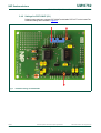
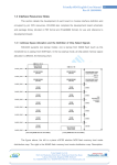
UM10762 User manual for the accurate RTC demo board OM13513 containing PCF2127T and PCF2129AT Rev. 2 — 1 September 2014 User manual Document information Info Content Keywords PCF2127T, PCF2129AT, OM13513, accurate RTC, Real-Time Clock, get started, SPI bus, I2C-bus, time stamp, temperature compensation, integrated quartz, tuning, battery switch, Watch-Dog Abstract User manual for the accurate RTC demo board OM13513 containing PCF2127T and PCF2129AT UM10762 NXP Semiconductors RTC PCF2127T, PCF2129AT evaluation board OM13513 Revision history Rev Date Description v.2 20140901 updated revision v.1 20140602 first revision Contact information For more information, please visit: http://www.nxp.com For sales office addresses, please send an email to: [email protected] UM10762 User manual All information provided in this document is subject to legal disclaimers. Rev. 2 — 1 September 2014 © NXP Semiconductors N.V. 2014. All rights reserved. 2 of 20 UM10762 NXP Semiconductors RTC PCF2127T, PCF2129AT evaluation board OM13513 1. Introduction The PCF2127, PCA2129 and PCF2129 are a family of very accurate Real-Time Clocks. They feature a fully integrated temperature compensated quartz oscillator (TCXO). Time stamp, battery management and watchdog blocks reduce the system overhead considerably. The OM13513 is the ideal evaluation and demo board to be used during the design phase of any project; only power and a serial bus (SPI-bus or I2C-bus) need to be connected. The OM13518 (USB to I2C-bus dongle) could be used for the I2C-bus connection. 2. Key features 2.1 Evaluation board OM13513 The accurate RTCs PCF2127T and PCF2129AT are mounted together with a back-up lithium battery on a small PC-board. Two push buttons allow initiating time stamps. All signals are accessible on the pin connectors P2 and P3 (see Figure 4), overcoming the need to build a test PC-board before the circuit can be evaluated or the functionality can be tested together with the final application. The board is also helpful to evaluate the functionality of PCF2127AT, PCF2129T and PCA2129T/Q900, the automotive grade version. Also check section Section 2.3. UM10762 User manual All information provided in this document is subject to legal disclaimers. Rev. 2 — 1 September 2014 © NXP Semiconductors N.V. 2014. All rights reserved. 3 of 20 UM10762 NXP Semiconductors RTC PCF2127T, PCF2129AT evaluation board OM13513 I2C SPI For configuring the board, see Section 3.4. Fig 1. OM13513 evaluation/demo board 2.2 Accurate RTC The specific features of the accurate RTC are complementing the main functionality. PCF2127T and PCF2129AT: • Temperature compensated quartz oscillator TCXO with embedded quartz crystal – Typical accuracy: 3 ppm • • • • Battery backup input pin and switch-over circuitry Battery backed output voltage Universal interface to select between SPI- and I2C-bus Time stamp facility – With interrupt capability – Detection of two different events on one multilevel input pin (for example, for tamper detection) • Programmable watchdog timer with interrupt UM10762 User manual All information provided in this document is subject to legal disclaimers. Rev. 2 — 1 September 2014 © NXP Semiconductors N.V. 2014. All rights reserved. 4 of 20 UM10762 NXP Semiconductors RTC PCF2127T, PCF2129AT evaluation board OM13513 • Programmable alarm function with interrupt capability In addition PCF2127T has the following features: • 512 Byte of battery buffered RAM • Programmable countdown timer with interrupt • Additional power fail detector to, for example, pre-alert the microcontroller that the power supply is going down The block diagram in Figure 2 nicely illustrates the key blocks: • • • • Fig 2. Time stamp facility Temperature compensated quartz oscillator TCXO Battery back-up switch Universal interface to select between SPI-bus and I2C-bus Block diagram of the accurate RTC family 2.3 Accurate Real-Time Clock PCF2127T, PCF2129AT The high accuracy is achieved by the integration of a temperature compensated quartz oscillator including the quartz crystal in one package. Additional features are battery management, time stamp facility and in case of the PCF2127T additional 512 bytes of battery buffered RAM. There are 3 different grades available: 1. Temperature compensation covering 25 C to +65 C: PCF2127AT, PCF2129AT (on the OM13513) UM10762 User manual All information provided in this document is subject to legal disclaimers. Rev. 2 — 1 September 2014 © NXP Semiconductors N.V. 2014. All rights reserved. 5 of 20 UM10762 NXP Semiconductors RTC PCF2127T, PCF2129AT evaluation board OM13513 2. Temperature compensation covering 40 C to +85 C: PCF2127T (on the OM13513), PCF2129T 3. Automotive grade AEC-Q100 covering 40 C to +85 C: PCA2129T/Q900 1. uses a quartz crystal packed in a metal can package. 2. and 3. use a quartz, packed in a ceramic package. 2.4 Expected accuracy The accuracy of an RTC is commonly specified in deviation of seconds per day or ppm; 1 s/day corresponds to 11.5ppm. The PCF2127AT and PCF2129AT are temperature compensated over the temperature range of 30 C to +60 C and the PCF2127T, PCF2129T and PCA2129T/Q900 are temperature compensated over the temperature range of 40 C to +85 C, see Figure 3. Since the actual deviations at different temperatures may be positive (running to fast) or negative (running too slow) they may cancel out each other to a high extend. Therefore the actual accuracy over timer is much better than specified in with the max values; < 3 ppm or 1 s/4days can be expected. Other consideration regard the ambient temperature over the day, respectively over the year. Temperatures below e.g. 15C and above +60 C are usually only present for a limited time of the day and may even not be present most of the year. UM10762 User manual All information provided in this document is subject to legal disclaimers. Rev. 2 — 1 September 2014 © NXP Semiconductors N.V. 2014. All rights reserved. 6 of 20 UM10762 NXP Semiconductors RTC PCF2127T, PCF2129AT evaluation board OM13513 001aaj650 40 Frequency stability (ppm) ± 10 ppm ± 5 ppm ± 10 ppm 0 (1) -40 PCF2127AT PCF2129AT (2) -80 -40 -20 0 20 40 60 80 100 Temperature (°C) 013aaa345 40 Frequency stability (ppm) ± 5 ppm ± 3 ppm ± 5 ppm 0 (1) -40 PCF2127T PCA2129T PCF2129T (2) -80 -40 Fig 3. UM10762 User manual -20 0 20 40 60 80 100 Temperature (°C) Temperature compensation gradation in respect to family All information provided in this document is subject to legal disclaimers. Rev. 2 — 1 September 2014 © NXP Semiconductors N.V. 2014. All rights reserved. 7 of 20 UM10762 NXP Semiconductors RTC PCF2127T, PCF2129AT evaluation board OM13513 3. Hardware setup GND VDD CLKOUT2 RSTn PFI PFOn CLKOUT1 TEST GND GND VDD SDA/CEn2 SCL SDI SDO SDA/CEn1 INTA1 TSn VDD U1 VDD U2 1 2 3 4 5 6 7 8 9 P3 1 2 3 4 5 6 7 8 9 P2 1 2 J2 1 2 J1 1 2 3 J3 J3 for futureuse SDA/CEn2 SDA/CEn1 3.1 Detailed circuit diagram P1 C1 SCL SCL1 INTA1 5V GND 3V3 Res SDA1 10uF GND VDD R1 2K2 SDA SDA2 Res 3V3 GND 5V INTA2 SCL2 14 13 12 11 10 9 8 7 6 5 4 3 2 1 1 Optional connector JP3 1 2 JP1 R5 2 47K JP2 1 R4 2 47K C3 IC1 SCL VDD SDI VBAT SDO BBS SDA/CEn INTn IFS n.c TSn n.c CLKOUT n.c VSS n.c n.c n.c n.c n.c 20 19 18 17 16 15 14 13 12 11 IC2 1 2 3 4 5 6 7 8 C2 100nF J4 PCF2129AT R3 220k IFS1 BBS VDD VBAT BBS INTn RSTn PFI PFOn TEST 16 15 14 13 12 11 10 9 C5 VSS 100nF 1 2 D1 GND R2 10k R6 820E IC2/PW 3 2 1 J5 BBS C4 JP4 IC1/PW VBAT 1 2 3 PCF2127T 100nF VSS IFS2 J7 VSS T1 1 2 3 100nF SCL SDI SDO SDA/CEn IFS TSn CLKOUT VSS T2 1 2 3 4 5 6 7 8 9 10 VSS 3 2 1 VBAT BT1 J6 3.3V CR2032 VDD M1 M2 Comment Comment GND Fig 4. Circuit diagram of the demo board OM13513 The position of the jumpers and connectors can be found in the circuit diagram (Figure 4) and the layout drawing (Figure 5). 3.2 General requirements for the PCF2127T and PCF2129AT The RTC circuit just requires a few external components to buffer the supply voltage. Avoid any tracks with high frequency signals (fast edges) close to the RTC or its connections. It is required to have a decoupling capacitor of 100 nF on the VDD-VSS rails close to the RTC; a similar decoupling capacitor on pin BBS is required. Due to the low power consumption of a few μW, no precautions for heat dissipations are required, even in a sealed housing environment. Frequencies of 1 Hz to 16.884 kHz at the CLKOUT pin can be used to measure the frequency for calibration and/or for general purpose use, e.g. as reference for the frequency generation with a PLL. If the CLKOUT frequency is set to 32.768 kHz, then the accuracy may be less. UM10762 User manual All information provided in this document is subject to legal disclaimers. Rev. 2 — 1 September 2014 © NXP Semiconductors N.V. 2014. All rights reserved. 8 of 20 UM10762 NXP Semiconductors RTC PCF2127T, PCF2129AT evaluation board OM13513 3.3 Battery back-up To guarantee the autonomy of the clock a continuous supply of power is needed. The battery back-up facility will assure this. For storage and delivery the jumpers J5 and J6 are set such that the battery will not be discharged. To reduce power consumption, always switch-off functions and outputs not in use. 3.4 Hardware settings 3.4.1 General settings • Set Jumper JP4 to activate LED D1 for signaling an interrupt • The single in line connectors P2 and P3 (100 mil pitch) give access to all pins for integrating the RTC into an application • Resistor R1 and C1 reduce the VDD slew rate when removing VDD to ensure clean battery switch over • A Lithium coin cell battery 2032 is mounted underneath the board to buffer the voltage in case of loss of supply voltage VDD • Jumper J1, respectively J2 allows to measure the current consumption, replace it by a A meter Fig 5. Evaluation board (top side layout) UM10762 User manual All information provided in this document is subject to legal disclaimers. Rev. 2 — 1 September 2014 © NXP Semiconductors N.V. 2014. All rights reserved. 9 of 20 UM10762 NXP Semiconductors RTC PCF2127T, PCF2129AT evaluation board OM13513 3.4.2 Settings for PCF2129AT (IC1) Default jumper settings to operate PCF2129AT and disable PCF2127T on the board.The hardware settings are illustrated in Figure 6. J I A D G VSS Fig 6. B C H K F E I2C SPI Hardware settings for PCF2129AT UM10762 User manual All information provided in this document is subject to legal disclaimers. Rev. 2 — 1 September 2014 © NXP Semiconductors N.V. 2014. All rights reserved. 10 of 20 UM10762 NXP Semiconductors RTC PCF2127T, PCF2129AT evaluation board OM13513 Table 1. Jumper settings to operate PCF2129AT (IC1) Description Jumper Setting[1] A VDD selected for PCF2129AT J1 ■■ B battery backup of PCF2129AT enabled J6 □■■ C battery backup of PCF2127T disabled J5 ■■□ D LED D1 connected to interrupt pin JP4 ■■ E I2C-bus selected for the PCF2129AT J4 □■■ Indicator Jumpers ■■□ SPI-bus selected for the PCF2129AT G unused SDI-interface connected to GND JP1 ■■ H pull-up on CLKOUT JP2 - supply and interface connector P2 - J interrupt output P2 - K clock output P3 - Interface I Outputs [1] In direction of reading “Jn”. UM10762 User manual All information provided in this document is subject to legal disclaimers. Rev. 2 — 1 September 2014 © NXP Semiconductors N.V. 2014. All rights reserved. 11 of 20 UM10762 NXP Semiconductors RTC PCF2127T, PCF2129AT evaluation board OM13513 3.4.3 Settings for PCF2127T (IC2) Default jumper settings to operate PCF2127T and disable PCF2129AT on the board.The hardware settings are illustrated in Figure 7. J I A M L D G VSS Fig 7. C B H K F E I2C SPI Hardware settings for PCF2127T UM10762 User manual All information provided in this document is subject to legal disclaimers. Rev. 2 — 1 September 2014 © NXP Semiconductors N.V. 2014. All rights reserved. 12 of 20 UM10762 NXP Semiconductors RTC PCF2127T, PCF2129AT evaluation board OM13513 Table 2. Jumper settings to operate the PCF2127T (IC2) Indicator Description Jumper A VDD selected for PCF2127T J2 B battery backup of PCF2127T enabled J5 C battery backup of PCF2129AT disabled J6 D LED D1 connected to interrupt pin JP4 F I2C-bus selected for the PCF2127T J7 Setting[1] Jumpers G unused SDI-interface connected to GND JP1 ■■ □■■ ■■□ ■■ □■■ ■■□ ■■ H pull-up on CLKOUT JP2 - supply and interface connector P2 - J interrupt output P2 - K clock output P3 - L time stamp input 1 T1 - M time stamp input 2 T1 - SPI-bus selected for the PCF2127T Interface I Outputs Push button [1] In direction of reading “Jn”. UM10762 User manual All information provided in this document is subject to legal disclaimers. Rev. 2 — 1 September 2014 © NXP Semiconductors N.V. 2014. All rights reserved. 13 of 20 UM10762 NXP Semiconductors RTC PCF2127T, PCF2129AT evaluation board OM13513 4. Optional features for test and evaluation 4.1 Experimental area Left of the NXP logo there is some space on the board where a custom circuitry can be placed. VSS and VDD are available for easy set up. 5. Software The accurate RTC is controlled via a standard SPI-bus or an FM+ I2C-bus interface. Common protocols apply. After power-up the control register has to be programmed first to set the correct functions and modes. Then the current time should be programmed. 5.1 Software instructions for setting the clock 5.1.1 Configuring the function Control registers 00h to 02h. 5.1.2 Setting the time Time and date registers 03h to 09h. 5.1.3 Programming alarms Alarm registers 0Ah to 0Eh. 5.1.4 Clock out control Register 0Fh. 5.1.5 Watchdog Registers 10h, 11h. 5.1.6 Time stamp Registers 12h to18h. 5.1.7 Aging compensation Register 19h. 5.1.8 RAM, PCF2127 only Registers 1Ah to 1Dh. 5.1.9 Frequency trimming Since the oscillator is factory calibrated, there is no need for trimming. Optional trimming can be done to compensate for aging or to set purposely an offset to the nominal frequency. Just program the register 19h accordingly. UM10762 User manual All information provided in this document is subject to legal disclaimers. Rev. 2 — 1 September 2014 © NXP Semiconductors N.V. 2014. All rights reserved. 14 of 20 UM10762 NXP Semiconductors RTC PCF2127T, PCF2129AT evaluation board OM13513 5.2 I2C-bus software example Set time to 9:45:37, Aug. 1 2014 Generate a blinking LED at the Seconds interrupt: Table 3. UM10762 User manual I2C-bus software example Address Value Function - S START condition - A2h slave address + R/W = 0 - 00h register address 00h 01h enable seconds interrupt 01h 00h default values 02h 00h default values 03h 37h set to 37 seconds 04h 45h set to 45 minutes 05h 09h set to 9 hours 06h 01h set to day 1 07h 05h set to Friday 08h 08h set to August 09h 14h set to year 14 - P STOP condition - S START condition - A2h slave address + R/W = 0 - 0Fh register address 0Fh 01h set CLKOUT frequency to 16 kHz 10h 23h select pulsed interrupt signal - P STOP condition All information provided in this document is subject to legal disclaimers. Rev. 2 — 1 September 2014 © NXP Semiconductors N.V. 2014. All rights reserved. 15 of 20 UM10762 NXP Semiconductors RTC PCF2127T, PCF2129AT evaluation board OM13513 6. References UM10762 User manual [1] PCF2127T — Accurate RTC with integrated quartz crystal for industrial [2] PCA2129T — Accurate RTC with integrated quartz crystal for automotive, data sheet [3] PCF2129AT — Integrated RTC, TCXO and quartz crystal [4] AN11266 — Application and soldering information for the PCF2127T industrial TCXO RTC, Application note [5] AN10857 — Application and soldering information for PCF2127A and PCF2129A TCXO RTC [6] AN11120 — Application and soldering information for the PCA2129 automotive TCXO RTC All information provided in this document is subject to legal disclaimers. Rev. 2 — 1 September 2014 © NXP Semiconductors N.V. 2014. All rights reserved. 16 of 20 UM10762 NXP Semiconductors RTC PCF2127T, PCF2129AT evaluation board OM13513 7. Legal information 7.1 Definitions Draft — The document is a draft version only. The content is still under internal review and subject to formal approval, which may result in modifications or additions. NXP Semiconductors does not give any representations or warranties as to the accuracy or completeness of information included herein and shall have no liability for the consequences of use of such information. 7.2 Disclaimers Limited warranty and liability — Information in this document is believed to be accurate and reliable. However, NXP Semiconductors does not give any representations or warranties, expressed or implied, as to the accuracy or completeness of such information and shall have no liability for the consequences of use of such information. NXP Semiconductors takes no responsibility for the content in this document if provided by an information source outside of NXP Semiconductors. In no event shall NXP Semiconductors be liable for any indirect, incidental, punitive, special or consequential damages (including - without limitation - lost profits, lost savings, business interruption, costs related to the removal or replacement of any products or rework charges) whether or not such damages are based on tort (including negligence), warranty, breach of contract or any other legal theory. Notwithstanding any damages that customer might incur for any reason whatsoever, NXP Semiconductors’ aggregate and cumulative liability towards customer for the products described herein shall be limited in accordance with the Terms and conditions of commercial sale of NXP Semiconductors. Right to make changes — NXP Semiconductors reserves the right to make changes to information published in this document, including without limitation specifications and product descriptions, at any time and without notice. This document supersedes and replaces all information supplied prior to the publication hereof. Suitability for use — NXP Semiconductors products are not designed, authorized or warranted to be suitable for use in life support, life-critical or safety-critical systems or equipment, nor in applications where failure or malfunction of an NXP Semiconductors product can reasonably be expected to result in personal injury, death or severe property or environmental damage. NXP Semiconductors and its suppliers accept no liability for inclusion and/or use of NXP Semiconductors products in such equipment or applications and therefore such inclusion and/or use is at the customer’s own risk. Applications — Applications that are described herein for any of these products are for illustrative purposes only. NXP Semiconductors makes no representation or warranty that such applications will be suitable for the specified use without further testing or modification. Customers are responsible for the design and operation of their applications and products using NXP Semiconductors products, and NXP Semiconductors accepts no liability for any assistance with applications or customer product UM10762 User manual design. It is customer’s sole responsibility to determine whether the NXP Semiconductors product is suitable and fit for the customer’s applications and products planned, as well as for the planned application and use of customer’s third party customer(s). Customers should provide appropriate design and operating safeguards to minimize the risks associated with their applications and products. NXP Semiconductors does not accept any liability related to any default, damage, costs or problem which is based on any weakness or default in the customer’s applications or products, or the application or use by customer’s third party customer(s). Customer is responsible for doing all necessary testing for the customer’s applications and products using NXP Semiconductors products in order to avoid a default of the applications and the products or of the application or use by customer’s third party customer(s). NXP does not accept any liability in this respect. Export control — This document as well as the item(s) described herein may be subject to export control regulations. Export might require a prior authorization from competent authorities. Evaluation products — This product is provided on an “as is” and “with all faults” basis for evaluation purposes only. NXP Semiconductors, its affiliates and their suppliers expressly disclaim all warranties, whether express, implied or statutory, including but not limited to the implied warranties of non-infringement, merchantability and fitness for a particular purpose. The entire risk as to the quality, or arising out of the use or performance, of this product remains with customer. In no event shall NXP Semiconductors, its affiliates or their suppliers be liable to customer for any special, indirect, consequential, punitive or incidental damages (including without limitation damages for loss of business, business interruption, loss of use, loss of data or information, and the like) arising out the use of or inability to use the product, whether or not based on tort (including negligence), strict liability, breach of contract, breach of warranty or any other theory, even if advised of the possibility of such damages. Notwithstanding any damages that customer might incur for any reason whatsoever (including without limitation, all damages referenced above and all direct or general damages), the entire liability of NXP Semiconductors, its affiliates and their suppliers and customer’s exclusive remedy for all of the foregoing shall be limited to actual damages incurred by customer based on reasonable reliance up to the greater of the amount actually paid by customer for the product or five dollars (US$5.00). The foregoing limitations, exclusions and disclaimers shall apply to the maximum extent permitted by applicable law, even if any remedy fails of its essential purpose. Translations — A non-English (translated) version of a document is for reference only. The English version shall prevail in case of any discrepancy between the translated and English versions. 7.3 Trademarks Notice: All referenced brands, product names, service names and trademarks are the property of their respective owners. All information provided in this document is subject to legal disclaimers. Rev. 2 — 1 September 2014 © NXP Semiconductors N.V. 2014. All rights reserved. 17 of 20 UM10762 NXP Semiconductors RTC PCF2127T, PCF2129AT evaluation board OM13513 8. Tables Table 1. Table 2. Table 3. Jumper settings to operate PCF2129AT (IC1) . 11 Jumper settings to operate the PCF2127T (IC2) . 13 I2C-bus software example . . . . . . . . . . . . . . . .15 UM10762 User manual All information provided in this document is subject to legal disclaimers. Rev. 2 — 1 September 2014 © NXP Semiconductors N.V. 2014. All rights reserved. 18 of 20 UM10762 NXP Semiconductors RTC PCF2127T, PCF2129AT evaluation board OM13513 9. Figures Fig 1. Fig 2. Fig 3. Fig 4. Fig 5. Fig 6. Fig 7. OM13513 evaluation/demo board . . . . . . . . . . . . .4 Block diagram of the accurate RTC family. . . . . . .5 Temperature compensation gradation in respect to family . . . . . . . . . . . . . . . . . . . . . . . . . . . . . . . . . . .7 Circuit diagram of the demo board OM13513 . . . .8 Evaluation board (top side layout) . . . . . . . . . . . . .9 Hardware settings for PCF2129AT . . . . . . . . . . .10 Hardware settings for PCF2127T . . . . . . . . . . . .12 UM10762 User manual All information provided in this document is subject to legal disclaimers. Rev. 2 — 1 September 2014 © NXP Semiconductors N.V. 2014. All rights reserved. 19 of 20 UM10762 NXP Semiconductors RTC PCF2127T, PCF2129AT evaluation board OM13513 10. Contents 1 2 2.1 2.2 2.3 2.4 3 3.1 3.2 3.3 3.4 3.4.1 3.4.2 3.4.3 4 4.1 5 5.1 5.1.1 5.1.2 5.1.3 5.1.4 5.1.5 5.1.6 5.1.7 5.1.8 5.1.9 5.2 6 7 7.1 7.2 7.3 8 9 10 Introduction . . . . . . . . . . . . . . . . . . . . . . . . . . . . 3 Key features . . . . . . . . . . . . . . . . . . . . . . . . . . . . 3 Evaluation board OM13513 . . . . . . . . . . . . . . . 3 Accurate RTC . . . . . . . . . . . . . . . . . . . . . . . . . . 4 Accurate Real-Time Clock PCF2127T, PCF2129AT . . . . . . . . . . . . . . . . . . . . . . . . . . . 5 Expected accuracy . . . . . . . . . . . . . . . . . . . . . . 6 Hardware setup . . . . . . . . . . . . . . . . . . . . . . . . . 8 Detailed circuit diagram . . . . . . . . . . . . . . . . . . 8 General requirements for the PCF2127T and PCF2129AT . . . . . . . . . . . . . . . . . . . . . . . . . . . 8 Battery back-up . . . . . . . . . . . . . . . . . . . . . . . . 9 Hardware settings. . . . . . . . . . . . . . . . . . . . . . . 9 General settings . . . . . . . . . . . . . . . . . . . . . . . . 9 Settings for PCF2129AT (IC1) . . . . . . . . . . . . 10 Settings for PCF2127T (IC2) . . . . . . . . . . . . . 12 Optional features for test and evaluation . . . 14 Experimental area . . . . . . . . . . . . . . . . . . . . . 14 Software . . . . . . . . . . . . . . . . . . . . . . . . . . . . . . 14 Software instructions for setting the clock . . . 14 Configuring the function . . . . . . . . . . . . . . . . . 14 Setting the time. . . . . . . . . . . . . . . . . . . . . . . . 14 Programming alarms . . . . . . . . . . . . . . . . . . . 14 Clock out control . . . . . . . . . . . . . . . . . . . . . . . 14 Watchdog . . . . . . . . . . . . . . . . . . . . . . . . . . . . 14 Time stamp . . . . . . . . . . . . . . . . . . . . . . . . . . . 14 Aging compensation . . . . . . . . . . . . . . . . . . . . 14 RAM, PCF2127 only . . . . . . . . . . . . . . . . . . . . 14 Frequency trimming . . . . . . . . . . . . . . . . . . . . 14 I2C-bus software example . . . . . . . . . . . . . . . 15 References . . . . . . . . . . . . . . . . . . . . . . . . . . . . 16 Legal information. . . . . . . . . . . . . . . . . . . . . . . 17 Definitions . . . . . . . . . . . . . . . . . . . . . . . . . . . . 17 Disclaimers . . . . . . . . . . . . . . . . . . . . . . . . . . . 17 Trademarks. . . . . . . . . . . . . . . . . . . . . . . . . . . 17 Tables . . . . . . . . . . . . . . . . . . . . . . . . . . . . . . . . 18 Figures . . . . . . . . . . . . . . . . . . . . . . . . . . . . . . . 19 Contents . . . . . . . . . . . . . . . . . . . . . . . . . . . . . . 20 Please be aware that important notices concerning this document and the product(s) described herein, have been included in section ‘Legal information’. © NXP Semiconductors N.V. 2014. All rights reserved. For more information, please visit: http://www.nxp.com For sales office addresses, please send an email to: [email protected] Date of release: 1 September 2014 Document identifier: UM10762