1
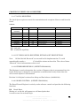
PCI-DMI32
User Manual
Preliminary
General Standards Corporation
8302A Whitesburg Drive
Huntsville, AL 35802
Phone: (256) 880-8787
Fax: (256) 880-8788
URL: www.generalstandards.com
E-mail: [email protected]
PREFACE
General Standards Corporation
Preliminary, Revised: December 1997
Copyright (C) 1999 General Standards Corp.
Additional copies of this manual or other literature may be obtained from:
General Standards Corporation
8302A Whitesburg Dr.
Huntsville, Alabama 35802
Tele: (256) 880-8787
FAX: (256) 880-8788
E-mail: [email protected]
The information in this document is subject to change without notice.
General Standards Corp. makes no warranty of any kind with regard to this material, including, but not limited to, the
implied warranties of merchantability and fitness for a particular purpose. Although extensive editing and reviews are
performed before release to ECO control, General Standards Corp. assumes no responsibility for any errors that may
exist in this document. No commitment is made to update or keep current the information contained in this document.
General Standards Corp. does not assume any liability arising out of the application or use of any product or circuit
described herein, nor is any license conveyed under any patent rights or any rights of others.
General Standards Corp. assumes no responsibility for any consequences resulting from omissions or errors in this
manual, or from the use of information contained herein.
General Standards Corp. reserves the right to make any changes, without notice, to this product to improve
reliability, performance, function, or design.
All rights reserved
No part of this document may be copied or reproduced in any form or by any means without prior written consent of
General Standards Corp.
This user’s manual provides information on the specifications, theory of operation, register level programming,
installation of the board and information required for customized hardware/software development.
User Manual for the PCI-DMI32, Manual Revision: A
General Standards Corporation
8302A Whitesburg Drive Huntsville, AL 35802, Phone: (256) 880-8787
II
RELATED PUBLICATIONS
The following manuals and specifications provide the necessary information for in depth understanding of the
specialized parts used on this board.
EIA Standard for the RS-422A Interface (EIA order number EIA-RS-422A)
PCI Local Bus Specification Revision 2.1 June 1, 1995. Questions regarding the PCI specification be forwarded to:
PCI Special Interest Group
P.O. Box 14070
Portland, OR 97214
(800) 433- 5177 (U.S.)
(503) 797-4207 (International)
(503) 234-6762 (FAX)
User Manual for the PCI-DMI32, Manual Revision: A
General Standards Corporation
8302A Whitesburg Drive Huntsville, AL 35802, Phone: (256) 880-8787
III
PCI-DMI32 DOCUMENTATION HISTORY
1) 03/20/2000: Converted PCI-HPDI32A Manual to PCI-HPDI32A-PRINT
2) 05/23/2001: Document Updates
User Manual for the PCI-DMI32, Manual Revision: A
General Standards Corporation
8302A Whitesburg Drive Huntsville, AL 35802, Phone: (256) 880-8787
IV
TABLE of CONTENTS
CHAPTER 1: INTRODUCTION.................................................................................................................................................5
1.0
1.2
FUNCTIONAL DESCRIPTION................................................................................................................................. 5
FIFOS ............................................................................................................................................................................ 7
CHAPTER 2: REGISTERS ..........................................................................................................................................................8
2.0
2.1
PCI-HPDI32-2GB-LVDS-A REGISTER INFORMATION...................... ERROR! B OOKMARK NOT DEFINED.
PCI CONFIGURATION REGISTERS ....................................................... ERROR! B OOKMARK NOT DEFINED .
Table 2.1-1:
2.2
Register Mapping.....................................................................................Error! Bookmark not defined.
PLX REGISTERS......................................................................................... ERROR! B OOKMARK NOT DEFINED .
Table 2.2-1:
Table 2.2-2:
Table 2.2-3:
Table 2.2-3:
LOCAL CONFIGURATION REGISTERS...............................................Error! Bookmark not defined.
RUN TIME REGISTERS............................................................................Error! Bookmark not defined.
DMA REGISTERS......................................................................................Error! Bookmark not defined.
MESSAGING QUEUE REGISTERS.........................................................Error! Bookmark not defined.
2.3
PCI CONFIGURATION REGISTER BIT MAPS..................................... ERROR! B OOKMARK NOT DEFINED .
2.3.1
PCI Configuration ID Register (Offset 0x00).................................................. Error! Bookmark not defined.
2.3.2
PCI Command Register (Offset 0x04) .............................................................. Error! Bookmark not defined.
2.3.3
PCI Status Register (Offset 0x06)..................................................................... Error! Bookmark not defined.
2.3.4
PCI Revision ID Register (Offset 0x08)........................................................... Error! Bookmark not defined.
2.3.5
PCI Class Code Register (Offset 0x09..0B) ..................................................... Error! Bookmark not defined.
2.3.6
PCI Cache Line Size Register (Offset 0x0C).................................................... Error! Bookmark not defined.
2.3.7
PCI Latency Timer Register (Offset 0x0D)...................................................... Error! Bookmark not defined.
2.3.8
PCI Header Type Register (Offset 0x0E)......................................................... Error! Bookmark not defined.
2.3.9
PCI Built-In Self Test (BIST) Register (PCI Offset 0x0F).............................. Error! Bookmark not defined.
2.3.10
PCI Base Address Register for Memory Access to Runtime Registers (Offset 0x010)..................Error!
Bookmark not defined.
2.3.11
PCI Base Address Register for I/O Access to Runtime Registers (Offset 0x14)..Error! Bookmark not
defined.
2.3.12
PCI Base Address Register for Memory Access to Local Address Space 0 (Offset 0x18) ...........Error!
Bookmark not defined.
2.3.13
PCI Base Address Register for Memory Access to Local Address Space 1 (Offset 0x1C)...........Error!
Bookmark not defined.
2.3.14
PCI Base Address Register (Offset 0x20)................................................. Error! Bookmark not defined.
2.3.15
PCI Base Address Register (Offset 0x24)................................................. Error! Bookmark not defined.
2.3.16
PCI Cardbus CIS Pointer Register (Offset 0x28)....................................... Error! Bookmark not defined.
2.3.17
PCI Subsystem Vendor ID Register (Offset 0x2C) ................................... Error! Bookmark not defined.
2.3.18
PCI Subsystem ID Register (Offset 0x2E).................................................. Error! Bookmark not defined.
2.3.19
PCI Expansion ROM Base Register (Offset 0x30) .................................... Error! Bookmark not defined.
2.3.20
PCI Interrupt Line Register (Offset 0x3C).................................................. Error! Bookmark not defined.
2.3.21
PCI Interrupt Pin Register (Offset 0x3D).................................................... Error! Bookmark not defined.
2.3.22
PCI Min_Gnt Register (Offset 0x3E)........................................................... Error! Bookmark not defined.
2.3.23
PCI Max_Lat Register (Offset 0x3F)........................................................... Error! Bookmark not defined.
2.4
LOCAL CONFIGURATION REGISTERS................................................ ERROR! B OOKMARK NOT DEFINED .
2.4.1
Local Address Space 0 Range Register for PCI to Local bus (PCI 0x00) (LOC 0x80)Error! Bookmark not
defined.
2.4.2
Local Address Space 0 Local Base Address (Re-map) Register for PCI to Local Bus (PCI 0x04) (LOC
0x84) Error! Bookmark not defined.
2.4.3
Mode/Arbitration Register (PCI 0x08) (LOC 0x88)........................................ Error! Bookmark not defined.
2.4.4
Big/Little Endian Descriptor Register (PCI 0x0C) (LOC 0x8C)..................... Error! Bookmark not defined.
User Manual for the PCI-DMI32, Manual Revision: A
General Standards Corporation
8302A Whitesburg Drive Huntsville, AL 35802, Phone: (256) 880-8787
1
2.4.5
Local Expansion ROM Range Register for PCI to Local Bus (PCI 0x10) (LOC 0x90) Error! Bookmark not
defined.
2.4.6
Local Expansion ROM Local Base Address (Re-map) register for PCI to Local Bus and BREQo Control
(PCI 0x14) (LOC 0x94)....................................................................................................... Error! Bookmark not defined.
2.4.7
Local Address Space 0/Expansion ROM Bus Region Descriptor Register (PCI 0x18) (LOC 0x98) ...Error!
Bookmark not defined.
2.4.8
Local Range register for Direct Master to PCI (PCI 0x1C) (LOC 0x9C) ...... Error! Bookmark not defined.
2.4.9
Local Bus Base Address register for Direct Master to PCI Memory (PCI 0x20) (LOC 0xA0).............Error!
Bookmark not defined.
2.4.10
Local Base Address for Direct Master to PCI IO/CFG Register (PCI 0x24) (LOC 0xA4)................Error!
Bookmark not defined.
2.4.11
PCI Base Address (Re-map) register for Direct Master to PCI Memory (PCI 0x28) (LOC 0xA8)..Error!
Bookmark not defined.
2.4.12
PCI Configuration Address Register for Direct Master to PCI IO/CFG (PCI 0x2C) (LOC 0xAC)..Error!
Bookmark not defined.
2.4.13
Local Address Space 1 Range Register for PCI to Local Bus (PCI 0xF0) (LOC 0x170)...................Error!
Bookmark not defined.
2.4.14
Local Address Space 1 Local Base Address (Remap) Register (PCI 0xF4) (LOC 0x174) ...............Error!
Bookmark not defined.
2.4.15
Local Address Space 1 Bus Region Descriptor Register (PCI 0xF8) (LOC 0x178)Error! Bookmark not
defined.
2.5
RUNTIME REGISTERS.............................................................................. ERROR! B OOKMARK NOT DEFINED .
2.5.1
Mailbox Register 0 (PCI 0x40) (LOC 0xC0)...................................................... Error! Bookmark not defined.
2.5.2
Mailbox Register 1 (PCI 0x44) (LOC 0xC4)...................................................... Error! Bookmark not defined.
2.5.3
Mailbox Register 2 (PCI 0x48) (LOC 0xC8)...................................................... Error! Bookmark not defined.
2.5.4
Mailbox Register 3 (PCI 0x4C) (LOC 0xCC) .................................................... Error! Bookmark not defined.
2.5.5
Mailbox Register 4 (PCI 0x50) (LOC 0xD0) ..................................................... Error! Bookmark not defined.
2.5.6
Mailbox Register 5 (PCI 0x54) (LOC 0xD4) ..................................................... Error! Bookmark not defined.
2.5.7
Mailbox Register 6 (PCI 0x58) (LOC 0xD8) ..................................................... Error! Bookmark not defined.
2.5.8
Mailbox Register 7 (PCI 0x5C) (LOC 0xDC).................................................... Error! Bookmark not defined.
2.5.9
PCI to Local Doorbell Register Description (PCI 0x60) (LOC 0xE0)............ Error! Bookmark not defined.
2.5.10
Local to PCI Doorbell Register Description (PCI 0x64) (LOC 0xE4)....... Error! Bookmark not defined.
2.5.11
Interrupt Control /Status (PCI 0x68) (LOC 0xE8) ...................................... Error! Bookmark not defined.
2.5.12
Serial EEPROM Control, PCI Command Codes, User I/O Control, Init Control Register (PCI 0x6C)
(LOC 0xEC)......................................................................................................................... Error! Bookmark not defined.
2.5.13
PCI Permanent Configuration ID Register (PCI 0x70) (LOC 0xF0) ........ Error! Bookmark not defined.
2.5.14
PCI Permanent Revision ID Register (PCI 0x74) (LOC 0xF4) ................. Error! Bookmark not defined.
2.6
LOCAL DMA REGISTERS........................................................................ ERROR! B OOKMARK NOT DEFINED .
2.6.1
DMA Channel 0 Mode Register (LOC 0x100)................................................ Error! Bookmark not defined.
2.6.2
DMA Channel 0 PCI Address Register (LOC 0x104).................................... Error! Bookmark not defined.
2.6.3
DMA Channel 0 Local Address Register (LOC 0x108) ................................ Error! Bookmark not defined.
2.6.4
DMA Channel 0 Transfer Size (Bytes) Register (LOC 0x10C)..................... Error! Bookmark not defined.
2.6.5
DMA Channel 0 Descriptor Pointer Register (LOC 0x110).......................... Error! Bookmark not defined.
2.6.6
DMA Channel 1 Mode Register (LOC 0x114)................................................ Error! Bookmark not defined.
2.6.7
DMA Channel 1 PCI Data Address Register (LOC 0x118) .......................... Error! Bookmark not defined.
2.6.8
DMA Channel 1 Local Data Address Register (LOC 0x11C) ...................... Error! Bookmark not defined.
2.6.9
DMA Channel 1 Transfer Size (bytes) register (LOC 0x120)....................... Error! Bookmark not defined.
2.6.10
DMA Channel 1 Descriptor Pointer Register (LOC 0x124)..................... Error! Bookmark not defined.
2.6.11
DMA Command/Status Register (LOC 0x128).......................................... Error! Bookmark not defined.
2.6.12
DMA Channel 1 Command/Status Register 0 (LOC 0x128).................... Error! Bookmark not defined.
2.6.13
DMA Arbitration Register 1 (LOC 0x12C) same as Mode /Arbitration Register at address (LOC 0x88)
Error! Bookmark not defined.
2.7
MESSAGING QUEUE REGISTERS.......................................................... ERROR! B OOKMARK NOT DEFINED .
2.7.1
Outbound Post List FIFO Interrupt Status Register (PCI 0x30) (LOC 0xB0)Error! Bookmark not defined.
User Manual for the PCI-DMI32, Manual Revision: A
General Standards Corporation
8302A Whitesburg Drive Huntsville, AL 35802, Phone: (256) 880-8787
2
2.7.2
2.7.3
2.7.4
2.7.5
2.7.6
2.7.7
2.7.8
2.7.9
2.7.10
2.7.11
2.7.12
2.7.13
2.7.14
2.7.15
Outbound Post List FIFO Interrupt Status Register (PCI 0x34) (LOC 0xB4)Error! Bookmark not defined.
Inbound Queue Port Register (PCI 0x40)........................................................ Error! Bookmark not defined.
Outbound Queue Port Register (PCI 0x44)..................................................... Error! Bookmark not defined.
Messaging Queue Configuration Register (PCI 0xC0) (LOC 0x140)........... Error! Bookmark not defined.
Queue Base Address Register (PCI 0xC4) (LOC 0x144) ............................... Error! Bookmark not defined.
Inbound Free Head Pointer Register (PCI 0xC8) (LOC 0x148)..................... Error! Bookmark not defined.
Inbound Free Head Tail Register (PCI 0xCC) (LOC 0x14C).......................... Error! Bookmark not defined.
Inbound Post Head Pointer Register (PCI 0xD0) (LOC 0x150) .................... Error! Bookmark not defined.
Inbound Post Tail Pointer Register (PCI 0xD4) (LOC 0x154).................. Error! Bookmark not defined.
Outbound Free Head Pointer Register (PCI 0xD8) (LOC 0x158)............. Error! Bookmark not defined.
Outbound Free Tail Pointer Register (PCI 0xDC) (LOC 0x15C).............. Error! Bookmark not defined.
Outbound Post Head Pointer Register (PCI 0xE0) (LOC 0x160)............. Error! Bookmark not defined.
Outbound Post Tail Pointer Register (PCI 0xE4) (LOC 0x164)................ Error! Bookmark not defined.
Queue Status/Control Register (PCI 0xE8) (LOC 0x168).......................... Error! Bookmark not defined.
2.8
PCI CONFIGURATION REGISTER BIT DESCRIPTIONS.................... ERROR! B OOKMARK NOT DEFINED .
2.8.1
PCI Configuration ID Register (Offset 0x00).................................................. Error! Bookmark not defined.
2.8.2
PCI Command Register (Offset 0x04) .............................................................. Error! Bookmark not defined.
2.8.3
PCI Status Register (Offset 0x06)..................................................................... Error! Bookmark not defined.
2.8.4
PCI Revision ID Register (Offset 0x08)........................................................... Error! Bookmark not defined.
2.8.5
PCI Class Code Register (Offset 0x09 - 0B).................................................... Error! Bookmark not defined.
2.8.6
PCI Cache Line Size Register (Offset 0x0C).................................................... Error! Bookmark not defined.
2.8.7
PCI Latency Timer Register (Offset 0x0D)...................................................... Error! Bookmark not defined.
2.8.8
PCI Header Type Register (Offset 0x0E)......................................................... Error! Bookmark not defined.
2.8.9
PCI Built-In Self Test (BIST) Register (PCI Offset 0x0F).............................. Error! Bookmark not defined.
2.8.10
PCI Base Address Register for Memory Access to Runtime Registers (Offset 0x010)..................Error!
Bookmark not defined.
2.8.11
PCI Base Address Register for I/O Access to Runtime Registers (Offset 0x14)..Error! Bookmark not
defined.
2.8.12
PCI Base Address Register for Memory Access to Local Address Space 0 (Offset 0x18) ...........Error!
Bookmark not defined.
2.8.13
PCI Base Address Register for Memory Accesses to Local Address Space 1 (Offset 0x1C).......Error!
Bookmark not defined.
2.8.14
PCI Base Address Register (Offset 0x20)................................................. Error! Bookmark not defined.
2.8.15
PCI Base Address Register (Offset 0x24)................................................. Error! Bookmark not defined.
2.8.16
PCI Base Cardbus CIS Pointer Register (Offset 0x28) ............................. Error! Bookmark not defined.
2.8.17
PCI Subsystem Vendor ID Register (Offset 0x2C) ................................... Error! Bookmark not defined.
2.8.18
PCI Subsystem ID Register (Offset 0x2E).................................................. Error! Bookmark not defined.
2.8.19
PCI Expansion ROM Base Register (Offset 0x30) .................................... Error! Bookmark not defined.
2.8.20
PCI Interrupt Line Register (Offset 0x3C).................................................. Error! Bookmark not defined.
2.8.21
PCI Interrupt Pin Register (Offset 0x3D).................................................... Error! Bookmark not defined.
2.8.22
PCI Min_Gnt Register (Offset 0x3E)........................................................... Error! Bookmark not defined.
2.8.23
PCI Max_Lat Register (Offset 0x3F)........................................................... Error! Bookmark not defined.
2.9
LOCAL CONFIGURATION REGISTERS BIT DESCRIPTIONS.................... ERROR! B OOKMARK NOT DEFINED .
2.9.1
Local Address Space 0 Range Register for PCI to Local bus (PCI 0x00) (LOC 0x80)Error! Bookmark not
defined.
2.9.2
Local Address Space 0 Local Base Address (Re-map) Register for PCI to Local Bus (PCI 0x04) (LOC
0x84) Error! Bookmark not defined.
2.9.3
Mode/Arbitration Register (PCI 0x08) (LOC 0x88)........................................ Error! Bookmark not defined.
2.9.4
Local Register (PCI 0x0C) (LOC 0x8C)............................................................. Error! Bookmark not defined.
2.9.5
Local Expansion ROM Range Register for PCI to Local Bus (PCI 0x10) (LOC 0x90)Error! Bookmark not
defined.
2.9.6
Local Expansion ROM Local Base Address (Re-map) register for PCI to Local Bus and BREQo Control
(PCI 0x14) (LOC 0x94)....................................................................................................... Error! Bookmark not defined.
User Manual for the PCI-DMI32, Manual Revision: A
General Standards Corporation
8302A Whitesburg Drive Huntsville, AL 35802, Phone: (256) 880-8787
3
2.9.7
Local Bus Region Descriptor for PCI to Local Accesses Register (PCI 0x18) (LOC 0x98)..................Error!
Bookmark not defined.
2.9.8
Local Range register for Direct Master to PCI (PCI 0x1C) (LOC 0x9C) ...... Error! Bookmark not defined.
2.9.9
Local Bus Base Address register for Direct Master to PCI Memory (PCI 0x20) (LOC 0xA0).............Error!
Bookmark not defined.
2.9.10
Local Base Address for Direct Master to PCI IO/CFG Register (PCI 0x24) (LOC 0xA4)................Error!
Bookmark not defined.
2.9.11
PCI Base Address (Re-map) register for Direct Master to PCI (PCI 0x28) (LOC 0xA8)..................Error!
Bookmark not defined.
2.9.12
PCI Configuration Address Register for Direct Master to PCI IO/CFG (PCI 0x2C) (LOC 0xAC)..Error!
Bookmark not defined.
2.9.13
Local Address Space 1 Range Register for PCI to Local Bus (PCI 0xF0) (LOC 0x170)...................Error!
Bookmark not defined.
2.9.14
Local Address Space 1 Local Base Address (Remap) Register (PCI 0xF4) (LOC 0x174) ...............Error!
Bookmark not defined.
2.9.15
Local Address Space 1 Bus Region Descriptor Register (PCI 0xF8) (LOC 0x178)Error! Bookmark not
defined.
2.10
SHARED RUNTIME REGISTERS BIT DESCRIPTIONS.............................. ERROR! B OOKMARK NOT DEFINED .
2.10.1
Mailbox Register 0 (PCI 0x40) (LOC 0xC0)................................................. Error! Bookmark not defined.
2.10.2
Mailbox Register 1 (PCI 0x44) (LOC 0xC4)................................................. Error! Bookmark not defined.
2.10.2
Mailbox Register 2 (PCI 0x48) (LOC 0xC8)................................................. Error! Bookmark not defined.
2.10.3
Mailbox Register 3 (PCI 0x4C) (LOC 0xCC) ............................................... Error! Bookmark not defined.
2.10.4
Mailbox Register 4 (PCI 0x50) (LOC 0xD0) ................................................ Error! Bookmark not defined.
2.10.5
Mailbox Register 5 (PCI 0x54) (LOC 0xD4) ................................................ Error! Bookmark not defined.
2.10.6
Mailbox Register 6 (PCI 0x58) (LOC 0xD8) ................................................ Error! Bookmark not defined.
2.10.7
Mailbox Register 7 (PCI 0x5C) (LOC 0xDC)............................................... Error! Bookmark not defined.
2.10.8
PCI to Local Doorbell Register Description (PCI 0x60) (LOC 0xE0)....... Error! Bookmark not defined.
2.10.9
Local to PCI Doorbell Register Description (PCI 0x64) (LOC 0xE4)....... Error! Bookmark not defined.
2.10.10
Interrupt Control /Status (PCI 0x68) (LOC 0xE8) ...................................... Error! Bookmark not defined.
2.10.11
EEPROM Control, PCI Command Codes, User I/O Control, Init Control Register (LOC 0xEC) ....Error!
Bookmark not defined.
2.10.12
PCI Permanent Configuration ID Register (PCI 0x70) (LOC 0xF0) ......... Error! Bookmark not defined.
2.10.13
PCI Permanent Revision ID Register (PCI 0x74) (LOC 0xF4) .................. Error! Bookmark not defined.
2.11
LOCAL DMA REGISTERS........................................................................ ERROR! B OOKMARK NOT DEFINED .
2.11.1
DMA Channel 0 Mode Register (LOC 0x100)........................................... Error! Bookmark not defined.
2.11.2
DMA Channel 0 PCI Address Register (LOC 0x104)............................... Error! Bookmark not defined.
2.11.3
DMA Channel 0 Local Address Register (LOC 0x108) ........................... Error! Bookmark not defined.
2.11.4
DMA Channel 0 Transfer Size (Bytes) Register (LOC 0x10C)................ Error! Bookmark not defined.
2.11.5
DMA Channel 0 Descriptor Pointer Register (LOC 0x110)..................... Error! Bookmark not defined.
2.11.6
DMA Channel 1 Mode Register (LOC 0x114)........................................... Error! Bookmark not defined.
2.11.7
DMA Channel 1 PCI Data Address Register (LOC 0x118) ..................... Error! Bookmark not defined.
2.11.8
DMA Channel 1 Local Data Address Register (LOC 0x11C) ................. Error! Bookmark not defined.
2.11.9
DMA Channel 1 Transfer Size (bytes) register (LOC 0x120).................. Error! Bookmark not defined.
2.11.10
DMA Channel 1 Descriptor Pointer Register (LOC 0x124)..................... Error! Bookmark not defined.
2.11.11
DMA Command/Status Register (LOC 0x128).......................................... Error! Bookmark not defined.
2.11.12
DMA Command/Status Register (LOC 0x129).......................................... Error! Bookmark not defined.
2.11.13
DMA Arbitration Register 0 (LOC 0x12C). Same as Mode/Arbitration Register at address ........Error!
Bookmark not defined.
2.11.14
DMA Threshold Register 1 (LOC 0x130)................................................... Error! Bookmark not defined.
2.12
MESSAGING QUEUE REGISTERS.......................................................... ERROR! B OOKMARK NOT DEFINED .
2.12.1
Outbound Post List FIFO Interrupt Status Register (PCI 0x30) (LOC 0xB0).........Error! Bookmark not
defined.
2.12.2
Outbound Post List FIFO Interrupt Status Register (PCI 0x34) (LOC 0xB4).........Error! Bookmark not
defined.
User Manual for the PCI-DMI32, Manual Revision: A
General Standards Corporation
8302A Whitesburg Drive Huntsville, AL 35802, Phone: (256) 880-8787
4
2.12.3
Inbound Queue Port Register (PCI 0x40)................................................... Error! Bookmark not defined.
2.12.4
Outbound Queue Port Register (PCI 0x44)................................................ Error! Bookmark not defined.
2.12.5
Messaging Queue Configuration Register (PCI 0xC0) (LOC 0x140)...... Error! Bookmark not defined.
2.12.6
Queue Base Address Register (PCI 0xC4) (LOC 0x144) .......................... Error! Bookmark not defined.
2.12.7
Inbound Free Head Pointer Register (PCI 0xC8) (LOC 0x148)................ Error! Bookmark not defined.
2.12.8
Inbound Free Head Tail Register (PCI 0xCC) (LOC 0x14C)..................... Error! Bookmark not defined.
2.12.9
Inbound Post Head Pointer Register (PCI 0xD0) (LOC 0x150) ............... Error! Bookmark not defined.
2.12.10
Inbound Post Tail Pointer Register (PCI 0xD4) (LOC 0x154).................. Error! Bookmark not defined.
2.12.11
Outbound Free Head Pointer Register (PCI 0xD8) (LOC 0x158)............. Error! Bookmark not defined.
2.12.12
Outbound Free Tail Pointer Register (PCI 0xDC) (LOC 0x15C).............. Error! Bookmark not defined.
2.12.13
Outbound Post Head Pointer Register (PCI 0xE0) (LOC 0x160)............. Error! Bookmark not defined.
2.12.14
Outbound Post Tail Pointer Register (PCI 0xE4) (LOC 0x164)................ Error! Bookmark not defined.
2.12.15
Queue Status/Control Register (PCI 0xE8) (LOC 0x168).......................... Error! Bookmark not defined.
2.13
PCI-HPDI32-2GB-LVDS-ALOCAL REGISTERS................................................................................................... 12
2.14
PCI-HPDI32-2GB-LVDS-ALOCAL REGISTERS, BIT MAP & BIT DESCRIPTIONS ..................................... 12
2.14.1
FIRMWARE REVISION: (Offset 0x00) ....................................................................................................... 12
2.14.2
BOARD CONTROL: (Offset 0x04)............................................................................................................... 12
2.14.3
BOARD STATUS: (Offset 0x08).................................................................................................................. 14
2.14.4
TX ALMOST: (Offset 0x0C)......................................................................................................................... 15
2.14.6
TX FIFOs: (Offset 0x18) ................................................................................................................................ 15
2.14.12
INTERRUPT CONTROL: (Offset 0x30)...................................................................................................... 15
2.14.13
INTERRUPT STATUS: (Offset 0x34).......................................................................................................... 16
CHAPTER 3: PROGRAMMING..............................................................................................................................................17
3.0
3.1
3.2
3.3
INITIALIZATION ...................................................................................... ERROR! B OOKMARK NOT DEFINED .
RESETS ........................................................................................................ ERROR! B OOKMARK NOT DEFINED .
FIFOS ............................................................................................................ ERROR! B OOKMARK NOT DEFINED .
INTERRUPTS.............................................................................................. ERROR! B OOKMARK NOT DEFINED.
CHAPTER 4: HARDWARE CONFIGURATION..................................................................................................................32
4.0
THE ON-BOARD TRANSMIT CLOCK ................................................................................................................ 32
Figure 4.0-1: Oscillator specification........................................................................................................................... 32
4.1
4.2
EEPROM JUMPER (J1)............................................................................................................................................ 32
CABLE CONNECTOR.............................................................................................................................................. 32
Table 4.2-1: Cable Pin-Out:
Cable Pin-Out Continued: ..........................................................................................33
CHAPTER 1: INTRODUCTION
2.4.2
FUNCTIONAL DESCRIPTION
The PCI-DMI32 Board provides a large on-board memory storage and high-speed, 32-bit
parallel interface. It is capable of transmitting or receiving data transfers of up to 200
Mbytes per second on the cable. The PCI-DMI32 Board includes up to 2GB of DRAM, a
cable input/output controller, cable transceivers (differential, LVDS), and a DMA
controller. The onboard memory can be configured to be accessed either from the PCI
bus, or dedicated to the cable transfer. The on-board DRAM does not provide real-time
access to the data from the PCI while a transfer is in progress. The DRAM should be
initialized via the PCI bus prior to the cable data transfer. When the transfer is enabled,
User Manual for the PCI-DMI32, Manual Revision: A
General Standards Corporation
8302A Whitesburg Drive Huntsville, AL 35802, Phone: (256) 880-8787
5
the cable data will be either continuously transmitted from the on-board DRAM, or
continuously received into the DRAM. Once the transfer is complete, the DRAM may be
again accessed from the PCI bus.
The transfer controller is designed to allow several different transfer modes. In single
transfer mode, a single buffer of data is transferred across the cable and then DRAM
control is returned to the PCI bus. The single buffer may start at any address offset
within the full 2GB DRAM space, and the transfer buffer size is also defined. In multibuffer mode, multiple buffers may be transferred across the cable. In this manner, the
user can define multiple buffers in the DRAM, which will then be transferred
continuously to the cable when the transfer is enabled. On-board interrupts are defined
to allow the user to update the start buffer address and buffer transfer size as soon as
the transfer of one buffer begins. In this manner, the user can dynamically receive or
transmit multiple buffers to/from the DRAM in one continuous transfer.
Likewise, a single buffer can be transmitted continuously to the cable simply by not
updating the start buffer address and buffer transfer size. This allows a continuous
buffer of up to 2GB to be transmitted indefinitely on the cable.
Note: The PCI-DMI32 is a long card and electrically compliant with PCI 2.1. Due to the
height of the DRAM modules, the card requires three PCI slots.
User Manual for the PCI-DMI32, Manual Revision: A
General Standards Corporation
8302A Whitesburg Drive Huntsville, AL 35802, Phone: (256) 880-8787
6
LVDS
User I/O
2GB DRAM
text
text
text
Addr
P
C
I
Addr
Addr
Ctrl
Data
Control
FPGA
Ctrl
Transmit
FIFO
PLX 9080
B
u
s
T
a
r
g
e
t
Data
Receive
FIFO
Data
LVDS
I
n
t
e
r
f
a
c
e
Data
Figure 1.0-2: Functional Block Diagram
2.4.3
1.1 CABLE INTERFACE
The cable interface consists of 32 bits of data, two clocks, and 14 user definable bi-directional
signals. All of which employ differential LVDS. Refer to cable pin-out Table 4.2-1.
2.4.4
1.2 DIMMS
The PCI-DIM32 board may be populated with up to four DIMMs for a total of 2 GB of
memory. Currently, the PCI-DMI32 supports 512MB SDRAM modules for a total of
512MB, 1GB, 1.5GB or 2GB of memory storage. General Standards Corporation is looking
into the possibility to migrate up/down using different density DIMMs. Please contact the
factory for more information and availability.
User Manual for the PCI-DMI32, Manual Revision: A
General Standards Corporation
8302A Whitesburg Drive Huntsville, AL 35802, Phone: (256) 880-8787
7
CHAPTER 2: PROGRAMMING
2.4.5
2.0 INITIALIZATION
Several functions on the PCI-DMI32 board will generally be unchanged in a given
application. These include interrupt setup and Users I/O direction setup.
Therefore, initializing these functions board will generally need to be done only
once by the software. However, if a Board Reset is performed, all registers will
return to their default values. Software must reinitialize the board following a
Board Reset. After a board reset is performed, the following will be true:
a. all cable transceivers will be turned off;
b. all interrupts will be disabled;
c. the SDRAM modules will be empty;
d. all RW registers will be set to 0 (Board Control Register bits are set to 0
on system reset)
2.4.6
RESETS
The Board Control Register contains a bit which are used to reset the local logic
functions. This bit performs a reset when the software writes a ‘1’. The reset bit
is also self-clearing, meaning software will not need to clear the bit following the
reset.
Board Reset
2.4.7
INTERRUPTS
Board Control Register D0 – Setting this bit will reset the
local logic, reset (clear) the FIFOs and SDRAM modules and
place all registers into a known state.
The PCI-DMI32 can generate 4 interrupts in response to the following conditions.
a. Data transfer on 32 bit data I/O started. Buffer has started to transmit.
b. Data transfer on 32 bit I/O done. Buffer has finished transmitting.
c. I/O user bit 6,13 when low, indicates new data on the user I/O input register.
This bit will be cleared upon reading the register.
d. PLX-DMA transfers done. Indicates the DMA has completed a transfer to or
from the host memory.
All interrupts will drive the PCI INT_A interrupt line.
2.4.8
DMA
Although the 33MHz PMC/PCI bus is capable of burst transfers up to 132Mbytes
per sec, actual sustained throughput on the PCI bus will be much lower. This is
due to many factors such as bus overhead, operating system overhead, application
overhead, and possibly data storage overhead such as hard disk drive accesses.
User Manual for the PCI-DMI32, Manual Revision: A
General Standards Corporation
8302A Whitesburg Drive Huntsville, AL 35802, Phone: (256) 880-8787
8
Since sustained PCI data rates will be typically slower than the maximum cable
interface rate, DMA on the PCI bus is supported to make the PCI data transfers
as fast as possible.
There are 3 methods the software application can move data to and from the PCIDMI32 board: PIO mode, Non-Demand DMA, and Demand Mode DMA. The two
DMA modes are only supported to the on-board SDRAM modules (DMA accesses
to local registers are not supported).
2.4.9
PIO MODE
In PIO mode, the user accesses the memory through single register reads and
writes to the board. This is the slowest data transfer mode.
2.4.10 NON-DEMAND DMA
In Non-Demand DMA mode, the user specifies a DMA transfer size and
initiates the transfer.
2.4.11 DEMAND MODE DMA
Demand Mode DMA is similar to Non-Demand DMA, except the local logic
will request the transfer based on FIFO status. After the user specifies a
DMA transfer size and initiates the transfer, the local logic will request the
data transfer if the Tx FIFO is not Full (transmit) or the Rx FIFO is not empty
(Rx FIFO). For transmit, the logic will burst data into the FIFO until the
Almost Full Flag is reached. The logic will then switch into a single transfer
mode until the FIFO is filled (or transfer is complete). When the Tx FIFO
becomes full, the logic will cease requesting data. When data is transmitted
out of the FIFO (Tx FIFO no longer full), the request will again be asserted to
re-fill the FIFO. This will resume until the transfer completes. When receive
Demand DMA is initiated, the DMA is requested whenever data is in the Rx
FIFO. On-board logic will run in burst mode until the Rx FIFO reaches the
Almost Empty level, at which time the logic will switch into single word mode,
where single words will be transferred until the FIFO goes empty. Once the
Rx FIFO is empty, the logic ceases to request data until more data is received.
The request is again asserted to empty the FIFO. This will continue until the
transfer completes. Demand Mode DMA is the preferred DMA method.
2.4.12 DMA DATA PACKING
DMA also provides a means to pack 16-bit or 8-bit data into 32bit transfers.
This is useful if only a 16-bit or 8-bit cable interface is used. In such cases,
each data word uses the full 32-bit FIFO width (data is not packed in FIFO),
but is packed for the PCI bus transfer. This will increase the effective PCI
data throughput.
User Manual for the PCI-DMI32, Manual Revision: A
General Standards Corporation
8302A Whitesburg Drive Huntsville, AL 35802, Phone: (256) 880-8787
9
2.4.13 CABLE INTERFACE SIGNALS
Cable data is transferred to and from the PCI-DMI32 board via a 100-pin cable
interface consisting of 50 differential signals – 1 Clock, 14 user I/O lines and 32
Data bits. The User I /O bits are divided into 2 logical blocks of 7 bits each. Each
block can be configured for input or output.
Data is transferred using the Cable Clock. All transmit data and user I/O signals
are clocked on the rising edge of the CLK signal. The transmit clock on the PCIDMI32 is supplied by an on-board oscillator. This oscillator is installed in sockets
so the user can customize the clock interface speed. The board is shipped with a
50MHz oscillator standard. To ensure maximum setup and hold times, all receive
data and user I/O signals are clocked on the falling edge of the CLK signal.
Figure 2.1 shows the data setup and hold times.
Clock Hi Time
19ns Min
Clock Low Time
19ns Min
Cable Clk
fmax = 25MHz
Transmit Clock
to
Cable Output
2ns Min
16ns Max
Receive Clock
to
Cable Input Setup
3ns Min
Cable Input Hold
from
Receive Clock
20ns Min
Cable I/O
FIGURE 2.1: CABLE INTERFACE TIMING
2.4.14 USER I/O SIGNALS
The 14 user I/O lines may be used as discrete I/O. This allows users to control
cable outputs, read cable inputs, or receive cable interrupts via simple software
control. The user I/O bits are controlled from the Board Control register. If a bit
is set as output, the Board Control register defines the output value. If a bit is
setup as an input, the state of the bit may be read through the Board Status
register. To set a user I/O signal as an interrupt source, set the signal as a input,
and setup the interrupt source via the interrupt registers.
2.4.15 TEST MODE
Test mode (D6) in the Board Control Register is intended for Board-to-Board
testing of two DMI cards. In normal mode, the DMI is connected to the SRI, and
the SRI provides the transfer clock. When in test mode, a DMI card will emulate
the SRI and provide the transfer clock to the second DMI card.
In test mode, the on board oscillator (50Mhz) is used as the transfer clock. The
DMI card in test mode will drive the test clock on the CLKIN signal and receive
User Manual for the PCI-DMI32, Manual Revision: A
General Standards Corporation
8302A Whitesburg Drive Huntsville, AL 35802, Phone: (256) 880-8787
10
the CLKOUT signal. Control Register bit D22 may be used to switch the test
clock to 25Mhz.
To simplify test mode, a jumper JP1 (J5: 7 to J5:8) has been dedicated to default
the DMI card to test mode. When jumper JP1 is removed from the card the Board
Control Register will reset to 0x00000050. This sets the test mode bit and sets
User port A to input, and User port B to output. Therefore, the two DMI cards
should each reset to the correct state for cable communication
2.4.16 DATA TRANSFERS
The DMI will transfer up to 2GB of unique data continuously at up to 50 Mhz. The data
transfer may be transmitted or received, depending on the direction set in the BCR.
Buffers may be transmitted or received indefinitely if the card is in multi buffer mode.
To initiate a transfer from the DMI card, the user should first initialize the on board
memory, set the DRAM start address and ram transfer count. This will define the buffer
to be transmitted or received. The user should then set the transfer direction and
multi/single buffer mode in the BCR. (It’s assumed the User I/O port directions have
been previously set). Once the transfer is setup, setting the start transfer bit D7 in the
BCR will initiate the transfer. At this point, the cable transceivers will be enabled. If the
DMI is in normal mode, the DMI will then transmit the Start Word from the Start Word
Register. Once the start word has been transmitted the DMI will began transmitting or
receiving the buffer. If in single buffer mode, the buffer will be transferred and the start
transfer bit will be cleared. If in multi buffer mode, the buffers will be transmitted until
the software clears the start transfer bit. After the first buffer has begun to transfer, the
start buffer interrupt will be asserted, and the user can update the DRAM start address
and transfer count for the next buffer. If the transfer count has not been updated before
the next buffer begins, the under run bit in the status register will indicate the under
run condition.
User Manual for the PCI-DMI32, Manual Revision: A
General Standards Corporation
8302A Whitesburg Drive Huntsville, AL 35802, Phone: (256) 880-8787
11
CHAPTER 3 PCI-DMI32 LOCAL REGISTERS
2.4.17 LOCAL REGISTERS
The Local Space registers control the transmission and reception of data to and from the
board
Table 3.0:
Offset Address
0x00000000x7FFFFFFF
0x80000000
0x80000004
0x80000008
0x8000000C
0x80000010
0x80000014
0x80000018
0x8000001C
Size
D32
Access*
RW
D32
D32
D32
D32
D32
D32
D32
D8
RO
RW
RO
RW
RW
RW
RW
RW
Register Name
Dram
Value after Reset
N/A
Firmware Revision
Board Control
Board Status
Dram Base Address
Dram Transfer Count
Interrupt Control
Interrupt Status
Start Word
0xXXXXXXXX
0x00000000
0xXXXXXCXX
0x00000000
0x00000000
0x00000000
0x00000000
0x78
RO - read only
RW - read/write capability
2.4.18 PCI-DMI32 LOCAL REGISTERS, BIT MAP & BIT DESCRIPTIONS
Note:
All bits labeled “Reserved” are unused in this implementation. To avoid
unpredictable results a
“0” should be written to these bits. The value of these
“Reserved” bits is indeterminate when read.
2.4.19 FIRMWARE REVISION: (OFFSET 0X800000000)
This Register is used to determine the version of firmware that is programmed into the
board. If the logic is changed to accommodate a modification for any reason then the
value in this register is incremented.
Revision 104: Original version after debug and final release. (0x00000104)
2.4.20 BOARD CONTROL: (OFFSET 0X800000004)
The Board Control Register is strictly under software control and provides the following
functions:
D0
Board Reset
Writing a 1 to this bit will generate a self-timed pulse that
is used to reset the on-board logic.
User Manual for the PCI-DMI32, Manual Revision: A
General Standards Corporation
8302A Whitesburg Drive Huntsville, AL 35802, Phone: (256) 880-8787
12
There is no need for the software to clear this bit, the bit will always read 0.
D1
CLKIN Check
Writing a 1 to this bit will check for a clock on the CLKIN signal of the cable.
There bit will automatically clear after the SYS. The results of the clock check operation
are reported in the Board Status Register.
D2
Transmit/Receive Direction
Writing a 1 to this bit will set the cable transfer direction to transmit.
Writing a 0 to this bit will set the cable transfer direction to receive.
D3
User I/O A Direction
Writing a 1 to this bit will set User I/O A port as an output port.
Writing a 0 to this bit will set User I/O A port as an input port.
D4
User I/O B Direction
Writing a 1 to this bit will set User I/O B port as an output port.
Writing a 0 to this bit will set User I/O B port as an input port.
Note: User I/O B port must be set to the opposite direction of the User I/O A port. If
both ports are set the same, only User I/O A will be enabled.
D5
Multi Buffer Mode
Writing a 1 to this bit will set the cable transfer to multi buffer mode. During transfers,
new buffers will continuously be loaded as the previous buffer completes.
Writing a 0 to this bit will set the cable transfer to single buffer mode. During the
transfer a single buffer will be transmitted and the transfer will automatically stop.
D6
Test Mode
Note:
Test mode is intended for loop back testing between two DMI Cards.
Writing a 1 to this bit will enable DMI test mode. When in test mode, the DMI card will
generate the clock to the CLKIN Signal and receive the clock from the CLKOUT signal
(opposite of normal DMI mode). The clock will be generated from an on-board 50Mhz
oscillator.
Writing a 0 to this bit will set the DMI in normal mode. This bit should be cleared if the
DMI is connected to the SRI or when connected to another DMI in test mode.
D7
Start Transfer
Writing a 1 to this bit will start data transferring on the cable. All other bits associated
with the data transfer should be set before (or at the same time) as the start transfer bit.
In Single Buffer Mode, this bit will clear automatically at the end of a transfer.
Writing a 0 to this bit will immediately terminate a transfer in progress, both multi
buffer mode and single mode.
D8..14
User I/O A Output
User Manual for the PCI-DMI32, Manual Revision: A
General Standards Corporation
8302A Whitesburg Drive Huntsville, AL 35802, Phone: (256) 880-8787
13
If user I/O A port is setup as output, these bits will be transmitted to the cable. These
bits will be output directly to the cable regardless of the start transfer mode bit. Bit D14
is defined as the valid bit for the output word.
D15..21 User I/O B Output
If user I/O B port is setup as output, these bits will be transmitted to the cable. These
bits will be output directly to the cable regardless of the start transfer mode bit. Bit D21
is defined as the valid bit for the output word.
D22
Internal Clock Speed
While in test mode (D5=1), this bit determines whether the transfer clock is 50Mhz or
25Mhz. Writing a 0 to this bit will set the internal test clock to 50Mhz, while a 1 will set
the internal test clock to 25Mhz.
D23..31
Reserved
2.4.21 BOARD STATUS: (OFFSET 0X800000008)
The Board Status Register is used to return information to the software about the most
current status of the board, at the time of the reading. Listed below is the information
that this register contains:
D0
CLKIN Present
A 1 indicates the CLKIN signal was detected during the CLKIN test (D1 of Board
Control Register). A 0 indicates no CLKIN present
D1
CLKIN Valid
A 1 indicates the “CLKIN present” (D0) bit is valid. A 0 indicates the CLKIN check test
is in progress.
D2..3
Reserved
D4
JP0
A 1 indicates the jumper JP0 has been removed.
D5
JP1
A 1 indicates the jumper JP1 has been removed.
D6..7
Reserved
D8..14 User I/O A Input
If User I/O A direction is set to input, these bits will show the last valid command
received. If User I/O A is set to output, these bits will show the current state of the
output port.
If User I/O A set to input, Bit D14 will indicate a new command has been received. (a
low-to-hi transition on User I/o bit 6). After the Board Status Register has been read,
this bit will clear until the next valid command is received.
User Manual for the PCI-DMI32, Manual Revision: A
General Standards Corporation
8302A Whitesburg Drive Huntsville, AL 35802, Phone: (256) 880-8787
14
D21..15 User I/O B Input
If User I/O B direction is set to input, these bits will show the last valid command
received. If User I/O B is set to output, these bits will show the current state of the
output port.
If User I/O B set to input, Bit D14 will indicate a new command has been received. (a
low-to-hi transition on User I/o bit 6). After the Board Status Register has been read,
this bit will clear until the next valid command is received.
D31..22 CLKIN Frequency Counter
Following a CLKIN test (D1 of the Board Control Register), this field contains the
number of CLKIN clocks during a 5us period. Using this count the CLKIN frequency
MHz can be determined using the following formula: Freq(MHz)=Count/5
2.4.22 DRAM BASE ADDRESS: (OFFSET 0X80000000C)
Starting Address of buffer for data transfer.
DRAMM TRANSFER COUNT: (Offset 0x800000010)
Number of bytes in buffer for data transfer.
Note: The DRAM BASE ADDRESS and DRAM TRANSFER COUNT must not exceed
the total memory size.
2.4.23 INTERRUPT CONTROL: (OFFSET 0X800000014)
D0
D1
D2
D3
D4..31
Enable Buffer Start Interrupt
Enable Buffer End Interrupt
Enable User I/O A Input Interrupt
Enable User I/O B Input Interrupt
Reserved
User Manual for the PCI-DMI32, Manual Revision: A
General Standards Corporation
8302A Whitesburg Drive Huntsville, AL 35802, Phone: (256) 880-8787
15
2.4.24 INTERRUPT STATUS: (OFFSET 0X800000018)
The Interrupt Status Register serves as a dual-purpose register. Each bit in this register
operates independently of each other. If an interrupt condition is enabled in the
Interrupt Control Register, the appropriate bit in the Interrupt Status Register will
indicate if an interrupt has occurred or not. When an interrupt occurs the status bit will
latch the interrupt condition until software resets it by writing a “1” to the appropriate
bit. If an interrupt is not enabled in the Interrupt Control Register, then the appropriate
bit in the Interrupt Status Register will indicate whether or not the condition currently
exists for an interrupt request. In this case, the interrupt condition is not latched and
does not need to be cleared by software.
Enable Buffer Start Interrupt
Enable Buffer End Interrupt
Enable User I/O A Input Interrupt
Enable User I/O B Input Interrupt
Under run status
This bit will be set in multibuffer mode when a new buffer was started
before the DRAM Transfer count register was reloaded.
D0
D1
D2
D3
D4
D5..31 Reserved
2.4.25 START WORD: (OFFSET 0X80000001C)
D0..6 This register contains the start command word to be transmitted when a
data transfer is initiated. This register defaults to 0x78 at reset, but may
be changed by the user if necessary.
D31..7 Reserved
User Manual for the PCI-DMI32, Manual Revision: A
General Standards Corporation
8302A Whitesburg Drive Huntsville, AL 35802, Phone: (256) 880-8787
16
CHAPTER 4: PCI INTERFACE
2.4.26 4.0 PCI INTERFACE REGISTERS
A PCI9080 I/O Accelerator from PLX Technology handles the PCI Interface. The
PCI interface is compliant with the 5V, 33MHz PCI Specification 2.1. The
PCI9080 provides dual DMA controllers for fast data transfers to and from the onboard FIFOs. Fast DMA burst accesses provide for a maximum burst throughput
of 132MB/s to the PCI interface. To reduce CPU overhead during DMA transfers,
the controller also implements Chained (Scatter/Gather) DMA, as well as
Demand Mode DMA.
Since many features of the PCI9080 are not utilized in this design, it is beyond the
scope of this document to duplicate the PCI9080 User’s Manual. Only those
features, which will clarify areas specific to the PCI/PMC-HPDI32, are detailed
here. Please refer to the PCI9080 User’s Manual (See Related Publications) for
more detailed information. Note that the BIOS configuration and software driver
will handle most of the PCI9080 interface. Unless the user is writing a device
driver, the details of the PCI interface (Chapter 2) may be skipped.
2.4.27 4.1 PCI CONFIGURATION REGISTERS
The PCI device configuration for the PCI-DMI32 is fully PCI 2.1 compliant. Table
4.1 contains a list of the PCI configuration registers present in the PCI9080. An
on-board configuration serial EEPROM initializes many of these registers.
Table 4.1:
PCI
CFG
Addr
PCI Configuration Registers
0x00
0x04
0x08
0x0C
Loca
l
Offs
et
Addr
0x00
0x04
0x08
0x0C
0x10
0x10
Local
Y
Local
Y[15:0],
Local
Y
0x14
0x14
Y
0x18
0x18
Y
0x1C
0x1C
Y
PCI/Loc
al
Writable
Register Name
Device ID/Vendor ID
Status/Command
Class Code/Revision ID
BIST (Unused)/Header Type/Latency
Timer/Cache Line Size
PCI Base Addr 0 for Memory Mapped
Local/Runtime/DMA Registers (PCIBAR0)
PCI Base Addr 1 for I/O Mapped
Local/Runtime/DMA Registers (PCIBAR1)
PCI Base Addr 2 for Local Addr Space 0
(PCIBAR2)
PCI Base Addr 3 for Local Addr Space 1
(PCIBAR3) (Unused)
User Manual for the PCI-DMI32, Manual Revision: A
General Standards Corporation
8302A Whitesburg Drive Huntsville, AL 35802, Phone: (256) 880-8787
Value after
Reset
0x908010B5
0x02800017
0x0680003
0x00002008
0x00000000
0x00000001
0x00000000
0x00000000
17
0x2C
0x30
0x2C
0x30
Local
Y
0x3C
0x3C
Y[7:0],
Local
Subsystem ID/Subsystem Vendor ID
PCI Base Address to Local Expansion ROM
(Unused)
0x90802400
0x00000000
Max_Lat/Min_Gnt/Interrupt Pin/Interrupt Line
0x00000100
Note: The Local Base Address for the PCI Configuration registers in Local Address
Space is 0xC0000000. However, there should be no need for the user to access the
PCI Configuration registers through Local Address Space.
2.4.28 PCI CONFIGURATION ID REGISTER
(Offset 0x00, Reset 0x908010B5)
D15:0 Vendor ID –– 0x10B5 = PLX Technology
D31:16 Device ID –– 0x9080 = PCI9080
2.4.29 PCI COMMAND REGISTER
(Offset 0x04, Reset 0x0017)
D0
D1
D2
D3
D4
D5
D6
continues.
D7
stepping.
D8
D9
I/O Space
A ‘1’ allows the device to respond to I/O space accesses.
Memory Space
A ‘1’ allows the device to respond to memory space accesses.
PCI Master Enable.
A ‘1’ allows the device to behave as a PCI bus master.
Note: This bit must be set for the PCI 9080 to perform DMA cycles.
Special Cycle. (Not Supported.)
Memory Write/Invalidate.
A ‘1’ enables memory write/invalidate.
VGA Palette Snoop. (Not Supported.)
Parity Error Response
A ‘0’ indicates that a parity error is ignored and operation
A ‘1’ indicates that parity checking is enabled.
Wait Cycle Control. Controls whether the device does address/data
A ‘0’ indicates the device never does address/data stepping.
Note: Hardcoded to 0.
SERR# Enable
A ‘1’ allows the device to drive the SERR# line.
Fast Back-to-Back Enable. Indicates what type of fast back-to-back
transfers a Master can perform on the bus.
A ‘1’ indicates fast back-to-back transfers can occur to any agent on
the bus.
User Manual for the PCI-DMI32, Manual Revision: A
General Standards Corporation
8302A Whitesburg Drive Huntsville, AL 35802, Phone: (256) 880-8787
18
A ‘0’ indicates fast back-to-back transfers can only occur to the same
agent as the previous cycle.
D15:10 Reserved
2.4.30 4.1.3
PCI STATUS REGISTER
(Offset 0x06, Reset 0x0280)
D5:0
D6
D7
D8
D10:9
D11
D12
D13
D14
D15
Reserved
User Definable Features Supported
A ‘1’ indicates UDF are supported.
Note: User Definable Features are Not Implemented
Fast Back-to-Back Capable.
A ‘1’ indicates the adapter can accept fast back-to-back transactions.
Master Data Parity Error Detected
A ‘1 indicates the following three conditions are met:
1. PCI9080 asserted PERR# itself or observed PERR#
asserted.
2. PCI9080 was bus master for the operation in which the
error occurred.
3. Parity Error Response bit in the Command Register is set.
Writing a ‘1’ to this bit clears the bit.
DEVSEL Timing. Indicates timing for DEVSEL# assertion.
A value of ‘01’ indicates a medium decode.
Note: Hardcode to 01.
Target Abort
A ‘1’ indicates the PCI9080 has signaled a target abort.
Writing a ‘1’ to this bit clears the bit.
Received Target Abort
A ‘1’ indicates the PCI9080 has received a target abort.
Writing a ‘1’ to this bit clears the bit.
Master Abort
A ‘1’ indicates the PCI9080 has generated a master abort signal.
Writing a ‘1’ to this bit clears the bit.
Signal System Error
A ‘1’ indicates the PCI9080 has reported a system error on the
SERR# signal.
Writing a ‘1’ to this bit clears the bit.
Detected Parity Error
A ‘1’ indicates the PCI9080 has detected a PCI bus parity error, even
if parity error handling is disabled (the Parity Error Response bit in
the Command Register is clear).
One of three conditions can cause this bit to be set:
1. PCI9080 detected a parity error during a PCI address
phase.
2. PCI9080 detected a data parity error when it was the
target of a write.
User Manual for the PCI-DMI32, Manual Revision: A
General Standards Corporation
8302A Whitesburg Drive Huntsville, AL 35802, Phone: (256) 880-8787
19
3. PCI9080 detected a data parity error when performing a
master read.
Writing a ‘1’ to this bit clears the bit.
2.4.31 4.1.4
PCI REVISION ID REGISTER
(Offset 0x08)
D7:0 Revision ID - The silicon revision of the PCI9080.
2.4.32 PCI CLASS CODE REGISTER
(Offset 0x09-0B, Reset=0x068000)
Register level programming interface
0x00 = Queue Ports at 0x40 and 0x44.
0x01 = Queue Ports at 0x40 and 0x44, Int Status and Int Mask at
0x30 and 0x34
D15:8 Sub-class Code - 0x80 = Other bridge device.
D23:16 Base Class Code. - 0x06 = Bridge Device
D7:0
2.4.33 PCI CACHE LINE SIZE REGISTER
(Offset 0x0C, Reset 0x00)
D7:0
System cache line size in units of 32-bit words.
2.4.34 PCI LATENCY TIMER REGISTER
(Offset 0x0D, Reset 0x00)
D7:0
PCI Latency Timer. Units of PCI bus clocks, the amount of time the
PCI9080, as a bus master, can burst data on the PCI bus.
2.4.35 PCI HEADER TYPE REGISTER
(Offset 0x0E, Reset 0x00)
D6:0
D7
Configuration Layout Type = 0
Header Type = 0.
2.4.36 PCI BASE ADDRESS REGISTER FOR MEMORY ACCESS TO
LOCAL/RUNTIME/DMA REGISTERS
(Offset 0x010, Reset 0x00000000)
D0
D2:1
Memory Space Indicator
A ‘0’ indicates register maps into Memory space.
Note: Hardcoded to 0.
Location of Register:
00 - Locate anywhere in 32-bit memory address space
User Manual for the PCI-DMI32, Manual Revision: A
General Standards Corporation
8302A Whitesburg Drive Huntsville, AL 35802, Phone: (256) 880-8787
20
Note: Hardcoded to 0.
D3
Prefetchable.
Note: Hardcoded to 0.
D7:4
Memory Base Address.
Default Size = 256 bytes.
Note: Hardcoded to 0.
D31:8 Memory Base Address.
Memory base address for access to Local, Runtime, and DMA
registers.
Note: PCIBAR0 is Memory Mapped Base Address of PCI9080 Registers
2.4.37 PCI BASE ADDRESS REGISTER FOR I/O ACCESS TO
LOCAL/RUNTIME/DMA REGISTERS
(Offset 0x14, Reset 0x00000001)
Memory Space Indicator
A ‘1’ indicates the register maps into I/O space.
Note: Hardcoded to 1.
D1
Reserved
D7:2
I/O Base Address.
Default Size = 256 bytes.
Note: Hardcoded to 0.
D31:8 I/O Base Address.
Base Address for I/O access to Local, Runtime, and DMA Registers.
Note: PCIBAR1 is I/O Mapped Base Address of PCI9080 Registers
D0
2.4.38 4.1.11
PCI BASE ADDRESS REGISTER FOR MEMORY ACCESS TO
LOCAL ADDRESS SPACE 0
(Offset 0x18, Reset 0x00000000)
D0
D2:1
D3
D31:4
Memory Space Indicator
A ‘0’ indicates register maps into Memory space.
(Specified in Local Address Space 0 Range Register - LAS0RR.)
Location of register (if memory space). Location values:
00 - Locate anywhere in 32-bit memory address space
(Specified in Local Address Space 0 Range Register - LAS0RR.)
Prefetchable
A ‘0’ indicates reads are not prefetchable.
(Specified in Local Address Space 0 Range Register - LAS0RR
Memory Base Address
Memory base address for access to Local Address Space 0.
2.4.39 PCI SUBSYSTEM DEVICE/VENDOR ID REGISTER
(Offset 0x2C, Reset 0x908010B5)
D15:0
Subsystem Vendor ID – 0x10B5 = PLX Technology
User Manual for the PCI-DMI32, Manual Revision: A
General Standards Corporation
8302A Whitesburg Drive Huntsville, AL 35802, Phone: (256) 880-8787
21
D31:16 Subsystem Device ID – 0x2400 = General Standards Corporation
HPDI32).
2.4.40 PCI INTERRUPT LINE REGISTER
(Offset 0x3C, Reset 0x00)
D7:0
Interrupt Line Routing Value.
Indicates which input of the system interrupt controller(s) to which
the interrupt line of the device is connected.
2.4.41 PCI INTERRUPT PIN REGISTER
(Offset 0x3D, Reset 0x01)
D7:0
Interrupt Pin register. Indicates which interrupt pin the device
uses.
01=INTA#
Note: PCI 9080 supports only one PCI interrupt pin (INTA#).
2.4.42 PCI MIN_GNT REGISTER
(Offset 0x3E, Reset 0x00)
D7:0
Minimum Grant
Specifies the minimum burst period the device needs assuming a
clock rate of 33 MHz. Value is in 250 nsec increments. A ‘0’
indicates no stringent requirement.
2.4.43 PCI MAX_LAT REGISTER
(Offset 0x3F, Reset 0x00)
D7:0
Maximum Latency
Specifies the maximum burst period the device needs assuming a
clock rate of 33 MHz. Value is in 250 nsec increments. A ‘0’
indicates no stringent requirement.
User Manual for the PCI-DMI32, Manual Revision: A
General Standards Corporation
8302A Whitesburg Drive Huntsville, AL 35802, Phone: (256) 880-8787
22
2.4.44 LOCAL CONFIGURATION REGISTERS
The Local Configuration registers give information on the Local side
implementation. Since Local Expansion ROM, Local Address Space 1, and Direct
Master accesses are not implemented on the PCI/PMC-HPDI32, the descriptions
of these registers have been omitted. Most of the Local Configuration Registers
are preloaded from the configuration Serial EEPROM at system reset.
Table 4.2: Local Configuration Registers
PCI
CFG
Addr
0x00
0x04
Local
Offset
Addr
0x80
0x84
PCI/Local
Writable
0x08
0x0C
0x10
0x88
0x8C
0x90
Y
Y
Y
0x14
0x94
Y
0x18
0x98
Y
0x1C
0x20
0x9C
0xA0
Y
Y
0x24
0xA4
Y
0x28
0xA8
Y
0x2C
0xAC
Y
0xF0
0x170
Y
0xF4
0x174
Y
0xF8
0x178
Y
Y
Y
Register Name
Range for PCI to Local Address Space 0
Local Base Address (Remap) for PCI to Local
Address Space 0 (Unused)
Mode/Arbitration Register
Big/Little Endian Descriptor
Range for PCI to Local Expansion ROM
(Unused)
Local Base Address (Re-map) for PCI to Local
Expansion ROM and BREQo control (Unused)
Local Bus Region Descriptions for PCI Local
Accesses
Range for Direct Master to PCI (Unused)
Local Base Address for Direct Master to PCI
Memory (Unused)
Local Base Address for Direct Master to PCI
Memory IO/CFG (Unused)
PCI Base Address (Re-map) for Direct Master
to PCI (Unused)
PCI Configuration Address Register for Direct
Master to PCI IO/CFG (Unused)
Range for PCI to Local Address Space 1
(Unused)
Local Base Address (Remap) for PCI to Local
Address Space 1 (Unused)
Local Bus Region Descriptor (Space 1) for PCI
to Local Accesses (Unused)
Value after
Reset
0xFFFFF000
0x00000000
0x00000000
0x00000000
0x00000000
0x00000000
0x00000000
0x00000000
0x00000000
0x00000000
0x00000000
0x00000000
0x00000000
0x00000000
0x00000000
2.4.45 LOCAL ADDRESS SPACE 0 RANGE REGISTER FOR PCI TO LOCAL BUS
(PCI 0x00, Reset 0xFFFFF000)
D0
Memory Space Indicator
A ‘0’ indicates register maps into Memory space.
User Manual for the PCI-DMI32, Manual Revision: A
General Standards Corporation
8302A Whitesburg Drive Huntsville, AL 35802, Phone: (256) 880-8787
23
D2:1
D3
D31:4
Location of register (if memory space). Location values:
00 - Locate anywhere in 32-bit memory address space
Prefetchable
A ‘0’ indicates reads are not prefetchable.
Specifies which PCI address bits will be used to decode a PCI access
to Local Address Space 0. A ‘1’ indicates bit is included in address
decode.
Local Address Space 0 value 0xFFFFF000 maps a 4kbyte range.
Since entire Local Address Space can be mapped into 4kb range, the remap
register is not used.
2.4.46 MODE/ARBITRATION REGISTER
(PCI 0x08)
D7:0
D8:15
D16
D17
D18
D20:19
D21
Local bus Latency Timer (Unused)
Local bus Pause Timer (Unused)
Local bus Latency Timer Enable (Unused)
Local bus Pause Timer Enable (Unused)
Local bus BREQ Enable (Unused)
DMA Channel Priority
00 = Rotational priority
01 = Channel 2 priority
10 = Channel 1 priority
11 = Reserved
Local bus direct slave give up bus mode
A value of 1 indicates local bus will be released when PCI9080 write FIFO empty or read
FIFO full.
D22
D23
D24
D25
D26
D27
D28
D29
D31:30
Direct slave LLOCKo# Enable (Unused)
PCI Request Mode
PCI Rev 2.1 Mode
PCI Read No Write Mode
PCI Read with Write Flush Mode
Gate the Local Bus Latency Timer with BREQ (Unused)
PCI Read No Flush Mode
Reads Device/Vendor ID or SubDevice/SubVendor ID
Reserved
2.4.47 BIG/LITTLE ENDIAN DESCRIPTOR REGISTER
(PCI 0x0C)
Since local bus is little endian, all bits should be left zero
2.4.48 LOCAL ADDRESS SPACE 0/EXPANSION ROM BUS REGION DESCRIPTOR
REGISTER
(PCI 0x18, Reset 0x40030143)
User Manual for the PCI-DMI32, Manual Revision: A
General Standards Corporation
8302A Whitesburg Drive Huntsville, AL 35802, Phone: (256) 880-8787
24
D1:0
D5:2
D6
D7
D8
D9
D10
D14:11
D15
D17:16
D21:18
D22
D23
D24
D25
D26
D27
D28:31
Memory Space 0 Local Bus Width
11 indicates 32-bit local bus
Memory Space 0 Internal Wait States
A ‘0’ indicates no wait states required
Memory Space 0 Ready Input Enable
A ‘1’ indicates Local Ready input enabled.
Memory Space 0 Bterm Input Enable (Unused)
Memory Space 0 Prefetch Disable (Unused)
Expansion ROM Space Prefetch Disable (Unused)
Read Prefetch Count Enable (Unused)
Prefetch Counter (Unused)
Reserved
Expansion ROM Space Local Bus Width (Unused)
Expansion ROM Space Internal Wait States (Unused)
Expansion ROM Space Ready Input Enable (Unused)
Expansion ROM Space Bterm Input Enable (Unused)
Memory Space 0 Burst Enable
Extra Long Load from Serial Enable
Expansion ROM Space Burst Enable (Unused)
Direct Slave PCI Write Mode
PCI Target Retry Delay Clocks
2.4.49 4.3 RUNTIME REGISTERS
The Runtime registers consist of mailbox registers, doorbell registers, and a
general-purpose control register. The mailbox and doorbell registers serve no
purpose on the PCI/PMC-HPDI32.
Table 4.3: Runtime Registers
PCI
CFG
Addr
0x40
0x44
0x48
0x4C
0x50
0x54
0x58
0x5C
0x60
0x64
0x68
Local
Offset
Addr
0xC0
0xC4
0xC8
0xCC
0xD0
0xD4
0xD8
0xDC
0xE0
0xE4
0xE8
PCI/Local
Writable
Y
Y
Y
Y
Y
Y
Y
Y
Y
Y
Y
Register Name
Mailbox Register 0 (Unused)
Mailbox Register 1 (Unused)
Mailbox Register 2 (Unused)
Mailbox Register 3 (Unused)
Mailbox Register 4 (Unused)
Mailbox Register 5 (Unused)
Mailbox Register 6 (Unused)
Mailbox Register 7 (Unused)
PCI to Local Doorbell Register (Unused)
Local to PCI Doorbell Register (Unused)
Interrupt Control/Status
User Manual for the PCI-DMI32, Manual Revision: A
General Standards Corporation
8302A Whitesburg Drive Huntsville, AL 35802, Phone: (256) 880-8787
Value after
Reset
0x00000000
0x00000000
0x00000000
0x00000000
0x00000000
0x00000000
0x00000000
0x00000000
0x00000000
0x00000000
0x00000000
25
0x6C
0x70
0x74
0x78
0x7C
0xEC
0xF0
0xF4
0xC0
0xC4
Y
N
N
Y
Y
General Purpose Control
Permanent Device ID/ Permanent Vendor ID
Permanent Revision ID
Mailbox Register 0 (Unused)
Mailbox Register 1 (Unused)
0x00000000
0x10B59080
0x0000000X
0x00000000
0x00000000
2.4.50 INTERRUPT CONTROL /STATUS
(PCI 0x68, Reset 0x00000000)
Enable Local bus LSERR# (Unused)
Enable Local bus LSERR# on a PCI parity error (Unused)
Generate PCI Bus SERR#
Mailbox Interrupt Enable (Unused)
Reserved
PCI Interrupt Enable
PCI Doorbell Interrupt Enable (Unused)
PCI Abort Interrupt Enable
PCI Local Interrupt Enable
Local Interrupt must be enabled for USC/FIFO interrupts.
D12
Retry Abort Enable (Unused)
D13
PCI Doorbell Interrupt Status.
D14
PCI Abort Interrupt Status
D15
PCI Local Interrupt Status
D16
Local Interrupt Output Enable
D17
Local Doorbell Interrupt Enable (Unused)
D18
Local DMA Channel 0 Interrupt Enable
D19
Local DMA Channel 1 Interrupt Enable
D20
Local Doorbell Interrupt Status
D21
DMA Channel 0 Interrupt Status
D22
DMA Channel 1 Interrupt Status
D23
BIST Interrupt Status
D24
A ‘0’ indicates a Direct Master was bus master during a Master or
Target abort.
D25
A ‘0’ indicates that DMA CH0 was bus master during a Master or
Target abort.
D26
A ‘0’ indicates that DMA CH1 was bus master during a Master or
Target abort.
D27
A ‘0’ indicates that a Target Abort was generated by the PCI9080
after 256 consecutive Master retries to a Target.
D31:28 PCI Mailbox 3:0 Write Status
D0
D1
D2
D3
D7:4
D8
D9
D10
D11
2.4.51 SERIAL EEPROM CONTROL, PCI COMMAND CODES, USER I/O
CONTROL, INIT CONTROL REGISTER
(PCI 0x6C, Reset 0x0x001767E)
User Manual for the PCI-DMI32, Manual Revision: A
General Standards Corporation
8302A Whitesburg Drive Huntsville, AL 35802, Phone: (256) 880-8787
26
D3:0
D7:4
D11:8
D15:12
D16
D17
D23:18
D24
EEPROM.
D25
D26
D27
D28
D29
D30
D31
PCI Read Command Code for DMA
PCI Write Command Code for DMA
PCI Memory Read Command Code for Direct Master (Unused)
PCI Memory Write Command Code for Direct Master (Unused)
General Purpose Output (Unused)
General Purpose Input (Unused)
Reserved
Serial EEPROM clock for Local or PCI bus reads or writes to Serial
Serial EEPROM chip select
Write bit to serial EEPROM
Read serial EEPROM data bit
Serial EEPROM present
Reload Configuration Registers
PCI Adapter Software Reset
Local Init Status
A ‘1’ indicates Local initialization done.
2.4.52 PCI PERMANENT CONFIGURATION ID REGISTER
(PCI 0x70, Reset 0x10B59080)
D15:0 Permanent Vendor ID (0x10B5)
D31:16 Permanent Device ID (0x9080)
2.4.53 PCI PERMANENT REVISION ID REGISTER
(PCI 0x74)
D7:0
Permanent Revision ID
User Manual for the PCI-DMI32, Manual Revision: A
General Standards Corporation
8302A Whitesburg Drive Huntsville, AL 35802, Phone: (256) 880-8787
27
2.4.54 4.4 LOCAL DMA REGISTERS
The Local DMA registers are used to setup the DMA transfers to and from the on-board
FIFOs. Since the PCI/PMC-HPDI32 is half-duplex (data is only transferred in one
direction at a time), only DMA Channel 0 is used.
Table 4.4: DMA Registers
PCI
CFG
Addr
Local
Offset
Addr
PCI/Local
Writable
0x80
0x84
0x88
0x8C
0x90
0x94
0x98
0x9C
0xA0
0xA4
0xA8
0x100
0x104
0x108
0x10C
0x110
0x114
0x118
0x11C
0x120
0x124
0x128
Y
Y
Y
Y
Y
Y
Y
Y
Y
Y
Y
0xAC
0xB0
0x12C
0x130
Y
Y
Register Name
DMA Channel 0 Mode Register
DMA Channel 0 PCI Address Register
DMA Channel 0 Local Address Register
DMA Channel 0 Transfer Byte Count Register
DMA Channel 0 Descriptor Pointer Register
DMA Channel 1 Mode Register (Unused)
DMA Channel 1 PCI Address Register (Unused)
DMA Channel 1 Local Address Register (Unused)
DMA Channel 1 Transfer Byte Count Register (Unused)
DMA Channel 1 Descriptor Pointer Register (Unused)
DMA Channel 1Command/Status Register
DMA Channel 0 Command/Status Register
DMA Mode/ Arbitration Register
DMA Threshold Register
Value
after
Reset
0x00000003
0x00000000
0x00000000
0x00000000
0x00000000
0x00000003
0x00000000
0x00000000
0x00000000
0x00000000
0x00000010
0x00000000
0x00000000
2.4.55 DMA CHANNEL 0 MODE REGISTER
(PCI 0x80)
D1:0
D5:2
D6
D7
D8
D9
Local Bus Width
00 = 8 bit DMA transfer width
01 = 16 bit DMA transfer width
10/11 = 32 bit DMA transfer width
Internal Wait States (Unused)
Ready Input Enable
Note: This bit should always be set to ‘1’ (Ready Input Enabled)
Bterm# Input Enable (Unused)
Note: This bit should always be set to ‘0’ (BTERM# Disabled)
Local Burst Enable
Note: If Burst enabled, the user must ensure FIFO will not become
empty (read) or full (write) during the burst access. For Demand
Mode DMA, this means the Almost Empty/Almost Full flags should
be set to a value of at least 8.
Chaining Enable
A ‘1’ indicates chaining mode is enabled.
User Manual for the PCI-DMI32, Manual Revision: A
General Standards Corporation
8302A Whitesburg Drive Huntsville, AL 35802, Phone: (256) 880-8787
28
D10
D11
D12
For chaining mode, the DMA source address, destination address
and byte count are loaded from memory in PCI Space.
Done Interrupt Enable
A ‘1’ enables interrupt when DMA done.
Note: If DMA clear count mode is enabled, the interrupt won’t
occur until the byte count is cleared.
Local Addressing Mode
A ‘1’ indicates local addresses LA [31:2] to be held constant.
Note: This bit should always be set to ‘1’ (no address increment)
Demand Mode Enable
A ‘1’ causes the DMA controller to operate in Demand Mode.
In Demand Mode, the DMA controller transfers data when its
DREQ# input is asserted. The DMA controller transfers Lwords
(32bits) of data. This may result in multiple transfers for an 8 or 16
bit bus.
D13
Write and Invalidate Mode for DMA Transfers
When set to 1, PCI 9080 performs Write and Invalidate cycles to the
PCI bus. PCI 9080 supports Write and Invalidate sizes of 8 or 16
Lwords. The size is specified in the PCI Cache Line Size Register. If
a size other than 8 or 16 is specified, PCI 9080 performs write
transfers rather than Write and Invalidate transfers. Transfers
must start and end at the Cache Line Boundaries.
D14
DMA EOT (End of Transfer) Enable (Unused)
D15
DMA Stop Data Transfer Mode
A’0’ sends a BLAST to terminate DMA transfer
Note: This bit should always be set to ‘0’.
D16
DMA Clear Count Mode (Unused)
D17
DMA Channel 0 Interrupt Select
A ‘1’ routes the DMA Channel 0 interrupt to the PCI interrupt.
Note: This bit should always be set to ‘1’.
D31:18 Reserved
2.4.56 DMA CHANNEL 0 PCI ADDRESS REGISTER
(PCI 0x84)
D31:0
PCI Address Register
2.4.57 DMA CHANNEL 0 LOCAL ADDRESS REGISTER
(PCI 0x88)
D31:0 Local Address Register
Note: Should be set to Local FIFO offset 0x18
2.4.58 DMA CHANNEL 0 TRANSFER SIZE (BYTES) REGISTER
(PCI 0x8C)
User Manual for the PCI-DMI32, Manual Revision: A
General Standards Corporation
8302A Whitesburg Drive Huntsville, AL 35802, Phone: (256) 880-8787
29
D22:0 DMA Transfer Size
D31:23 Reserved
2.4.59 DMA CHANNEL 0 DESCRIPTOR POINTER REGISTER
(PCI 0x90)
Descriptor Location
A ‘1’ indicates PCI address space.
Note: This bit should always be set to ‘1’ if Chained DMA enabled.
D1
End of Chain
D2
Interrupt after Terminal Count
D3
Direction of transfer
A ‘1’ indicates transfers from local bus to PCI bus (Read Receive
FIFO)
A ‘0’ indicates transfers from local bus to PCI bus (Write Transmit
FIFO)
D31:4 Next Descriptor Address
D0
2.4.60 DMA CHANNEL 0 COMMAND/STATUS REGISTER
(PCI 0xA8)
D0
D1
D2
D3
D4
D7:5
Channel 0 Enable
Channel 0 Control
Channel 0 Abort
Clear Interrupt
Channel 0 Done
Reserved
2.4.61 DMA ARBITRATION REGISTER
(PCI 0xAC)
Same as Mode /Arbitration Register (MARBR) (PCI 0x08 – See Section 2.2.2)
2.4.62 DMA THRESHOLD REGISTER
(PCI 0xB0)
D3:0
D7:4
D11:8
D15:12
D19:16
D23:20
D27:24
D31:28
DMA Channel 0 PCI to Local Almost Full (C0PLAF)
DMA Channel 0 Local to PCI Almost Empty (C0LPAE)
DMA Channel 0 Local to PCI Almost Full (C0LPAF)
DMA Channel 0 PCI to Local Almost Empty (C0PLAE)
DMA Channel 1 PCI to Local Almost Full (C1PLAF) (Unused)
DMA Channel 1 Local to PCI Almost Empty (C1LPAE) (Unused)
DMA Channel 1 PCI to Local Almost Full (C1LPAF) (Unused)
DMA Channel 1 PCI to Local Almost Empty (C1PLAE) (Unused)
User Manual for the PCI-DMI32, Manual Revision: A
General Standards Corporation
8302A Whitesburg Drive Huntsville, AL 35802, Phone: (256) 880-8787
30
2.4.63 4.5 MESSAGING QUEUE REGISTERS
Messaging queue registers are not used on the PCI -DMI32.
User Manual for the PCI-DMI32, Manual Revision: A
General Standards Corporation
8302A Whitesburg Drive Huntsville, AL 35802, Phone: (256) 880-8787
31
CHAPTER 5: HARDWARE CONFIGURATION
2.4.64 THE ON-BOARD TRANSMIT CLOCK
The on-board oscillator, U11, is used as the transmit clock while in test mode. The oscillator is factory installed at
50MHz. This oscillator can be changed in the field by the end user. The maximum frequency supported by this clock
is 50Mhz.
1 8
4 5
Pin
1
4
5
8
Name
NC
GND
OUT
VDD
8 pin oscillator pin-out
Figure 4.0-1: Oscillator specification
JUMPERS (J5)
J5 is a header consisting of four individual jumpers.
J5: 1 to J5: 2
7
1
8
2
J5
EEPROM Configuration
This jumper connects the PNP EEPROM to the PCI chipset for power-up configuration. This jumper is intended for
factory use only and should always be installed.
J5: 3 to J5: 4
FPGA Reload
This jumper connects the FPGA Reload to the local PCI. When this jumper is installed, the FPGA will reload when the
PCI is reset. If the jumper is off, the FPGA will reload only at power-up. This jumper is intended for factory use only
and should always be installed.
J5: 5 to J5: 6
JP0
This jumper is a general-purpose jumper, which may be read from the Board Status Register (D?). If two identical DMI
cards are present in one system, this jumper may be removed on one card to provide a means to distinguish the cards
via software.
J5: 7 to J5: 8
JP1(Test Mode Jumper)
When this jumper is removed, the card will reset to Test mode if D6 is set in the Board Control Register. The User I/O
ports will also default to port A as input and port B as output. This bit may be read from D4 & 5 of the Board Status
Register.
4.2
CABLE CONNECTOR
User Manual for the PCI-DMI32, Manual Revision: A
General Standards Corporation
8302A Whitesburg Drive Huntsville, AL 35802, Phone: (256) 880-8787
32
The 80-pin user connector (reference designator: P1) is manufactured by Robinson Nugent, the part number is
P50E-080-P1-SR1-TG. The part number for the mate is P50E-080-S-TG, (50 mil. cabling is suggested for twisted pair), or
P25E-080S-TG (25 mil. cabling may be used for multi-drop capability, but with loss of twisted pair).
Table 4.2-1:
Pin No.
1A
2A
3A
4A
5A
6A
7A
8A
9A
10A
11A
12A
13A
14A
15A
16A
17A
18A
19A
20A
21A
22A
23A
24A
25A
26A
27A
28A
29A
30A
31A
32A
33A
34A
35A
36A
37A
38A
39A
40A
41A
42A
43A
44A
45A
46A
47A
48A
49A
50A
Cable Pin-Out:
Cable Signal Name
Pin No.
CLK IN +(CLK FROM SRI)
USER D0 +
USER D1 +
USER D2 +
USER D3 +
USER D4 +
USER D5 +
USER D6 +
USER D7 +
USER D8 +
USE R D9 +
USER D10 +
USER D11 +
USER D12 +
USER D13 +
CLOCK OUT +(CLK TO SRI)
I/O D0 +
I/O D1 +
I/O D2 +
I/O D3 +
I/O D4 +
I/O D5 +
I/O D6 +
I/O D7 +
I/O D8 +
I/O D9 +
I/O D10 +
I/O D11 +
I/O D12 +
I/O D13 +
I/O D14 +
I/O D15 +
I/O D16 +
I/O D17 +
I/O D18 +
I/O D19 +
I/O D20 +
I/O D21 +
I/O D22 +
I/O D23 +
I/O D24 +
I/O D25 +
I/O D26 +
I/O D27 +
I/O D28 +
I/O D29 +
I/O D30 +
I/O D31 +
GND
GND
1B
2B
3B
4B
5B
6B
7B
8B
9B
10B
11B
12B
13B
14B
15B
16B
17B
18B
19B
20B
21B
22B
23B
24B
25B
26B
27B
28B
29B
30B
31B
32B
33B
34B
35B
36B
37B
38B
39B
40B
41B
42B
43B
44B
45B
46B
47B
48B
49B
50B
Cable Signal Name
CLK IN -(CLK FROM SRI)
USER D0 USER D1 USER D2 USER D3 USER D4 USER D5 USER D6 USER D7 USER D8 USER D9 USER D10 USER D11 USER D12 USER D13 CLOCK OUT -(CLK TO SRI)
I/O D0 I/O D1 I/O D2 I/O D3 I/O D4 I/O D5 I/O D6 I/O D7 I/O D8 I/O D9 I/O D10 I/O D11 I/O D12 I/O D13 I/O D14 I/O D15 I/O D16 I/O D17 I/O D18 I/O D19 I/O D20 I/O D21 I/O D22 I/O D23 I/O D24 I/O D25 I/O D26 I/O D27 I/O D28 I/O D29 I/O D30 I/O D31 GND
GND
User Manual for the PCI-DMI32, Manual Revision: A
General Standards Corporation
8302A Whitesburg Drive Huntsville, AL 35802, Phone: (256) 880-8787
33