1
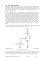
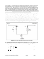
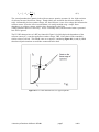
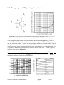
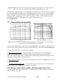
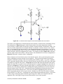
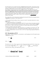
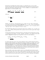
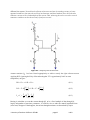
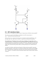
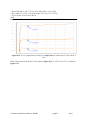
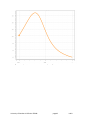
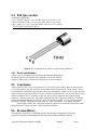
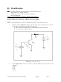
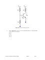
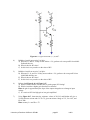
Laboratory Experiment 8 EE348L B.Madhavan Revised by: Aaron Curry University of Southern California. EE348L page1 Lab 8 Table of Contents 8 Experiment #8: Introduction to the Bipolar Junction Transistor ....................... 4 8.1 Introduction ............................................................................................................................. 4 8.2 Bipolar Junction Transistor Theory:....................................................................................... 4 8.2.1 Linear Region of operation: ................................................................................................... 5 8.2.2 Biasing and general BJT operating point considerations....................................................... 8 8.2.3 Choice of collector current and beta ...................................................................................... 9 8.2.4 Biasing a common-emitter amplifier with emitter degeneration resistor ............................... 9 8.2.5 Determinitaion of VCE ……………………………………………………………………...11 8.2.6 Wilson Current Source........................................................................................................ 14 8.3 BJT simulation in HSpice.................................................................................................... 15 8.4 BJT Spice models................................................................................................................ 19 8.4.1 Device Specifications:......................................................................................................... 19 8.5 Conclusion ........................................................................................................................... 19 8.6 Revision History.................................................................................................................. 19 8.7 References ........................................................................................................................... 20 8.8 Pre-lab Exercises ................................................................................................................. 21 8.9 Lab Exercises....................................................................................................................... 25 University of Southern California. EE348L page2 Lab 8 Table of Figures Figure 8-1: Device-level representations of (a) npn & (b) pnp bipolar transistors, and their schematic symbols (c) and (d), respectively. ……........................................................... 4 Figure 8-2: NPN transistor with forward bias across base-emitter junction and resistive load attached between collector and power supply. ................................................................ 5 Figure 8-3: The large signal model of a forward active biased BJT.................................................... 6 Figure 8-4: IC-VBE characteristics of a typical npn BJT.................................................................... 7 Figure 8-5: (a) DC voltage and current variables associated with an npn BJT and (b) VCE(sat) as a function of IC at 25˚C for general-purpose discrete npn BJT, 2N3904, used in this laboratory experiment. ............................................................................................................ 8 Figure 8-6: Data sheet curves associated with general purpose 2N3904 npn BJT. (a) VBE versus IC at 125˚C, 25˚C, and –40˚C and (b) IC versus VCE for different IB values at 25˚C………………………………………………………………………………………………… ... 9 Figure 8-7: Data sheet curves associated with general purpose 2N3904 npn BJT. (a) ac current- gain versus IC and (b) fT versus IC at 25˚C and VCE=5V. .................................... 9 Figure 8-8: A common-emitter amplifier with emitter degeneration resistor Ree. ............................ 10 Figure 8-9: Simple bipolar current mirror. ........................................................................................ 13 Figure 8-10: Wilson current source. ................................................................................................. 15 Figure 8-11: Spice netlist for obtaining I-V characteristic of an npn BJT, 2N3904........................ 17 Figure 8-12: IC-VCE characteristics of BJT q1 in Figure 8-11 for VBE of 0.65V, 0.68V and 0.7V volts. ...................................................................................................................... 17 Figure 8-13: β versus VBE characteristics of BJT q1 in Figure 8-11 for VCE=3.5 V at 27˚C. ........ 18 Figure 8-14: 2N3904 pin out (Courtesy of Fairchild Semiconductor). .............................................. 19 Figure 8-15: Figure for Prelab 1. ...................................................................................................... 21 Figure 8-16: Figure for Prelab 2, 4, and 6......................................................................................... 22 Figure 8-17: Figure for Prelab 3, 5, 6, and 7..................................................................................... 23 University of Southern California. EE348L page3 Lab 8 8 Experiment #8: Introduction Bipolar Junction Transistor to the 8.1 Introduction Transistors are at the heart of integrated circuit design. As active elements, they are capable of implementing gain stages, buffers, electrically operable switches, op-amps and a host of other applications that require active elements. The word active refers to the fact that transistors require static power, in the form of bias current and/or voltage, to operate in the desired operating region. It is desired, more often than not, that transistors in analog circuits be biased in their active or linear region. The static power provided by the bias is consumed so that input signals may be amplified. In other words, signals experience gain at the expense of static power consumption in the circuit. This experiment will deal with the static, or DC, behavior of the npn Bipolar Junction Transistor (BJT). A brief theory of operation will be presented, and then biasing and their use as current sources will be explored. In the next lab, gain and the dynamic aspects of transistors will be explored. 8.2 Bipolar Junction Transistor Theory: Bipolar junction transistors can be viewed as an arrangement of two integrate, back-to-back pn junction diodes, as shown in Figure 8-1. Figure 8-1: Device-level representations of (a) npn & (b) pnp bipolar transistors, and their schematic symbols (c) and (d), respectively. For any discussion that pertains to npn transistors in this experiment, the same discussion applies to pnp transistors provided in every instance “n” be replaced by “p”. Every equation for the npn transistor related to the dc operation of the device can be modified and used for the pnp transistor. This is accomplished by reversing the direction of all currents and the polarity of all voltages. University of Southern California. EE348L page4 Lab 8 8.2.1 Linear Region of operation: In analog circuits, the BJT is biased in the forward active region (a.k.a. linear active) to achieve high gain and linear operation. In order to bias a BJT in the forward-active operation, the base-emitter junction is forward biased, while the base-collector junction reverse biased. The base-emitter voltage (VBE) drop will be around 700mV for a silicon BJT. VBE may deviate a little from 700mV due to the inherent exponential I-V characteristics of the device. The emitter is highly doped n+ material (i.e., low impedance), so electrons are injected quite easily into the base under forward bias. The base is doped moderately relative to the emitter, implying that the base-emitter depletion region lies almost entirely on the base side of the junction. Furthermore, the base is a very narrow region; thus the associated electric field is quite large. This electric filed sweeps the injected electrons right through to the collector (actually, due to the finite base width, and associated finite transit time, a few electrons recombine with available holes in the base before diffusing to the base-collector depletion region, but this is not a dominant effect in modern processes). These electrons are the minority charge necessary to supply the reverse current through the reverse-biased base- collector junction. It is the forward bias across the baseemitter junction that supplies this charge, thus the current through the base-collector junction is not limited to the negligible reverse saturation current. In fact, neglecting recombination of the electrons in transit with available holes in the base, the current through the collector is practically identical to the current through the emitter. The utility of the transistor becomes apparent if one explores what happens if the current injected into the collector is allowed to flow into a resistive load, as shown in Figure 8-2. Figure 8-2: NPN transistor with forward bias across base-emitter junction and resistive load attached between collector and power supply As the base and power supply voltages are fixed, it follows that varying the load resistance causes a varying collector node voltage to develop. Thus, the base-collector reverse bias changes. However, recall from the diode labs that the magnitude of the reverse bias voltage has very little effect on the University of Southern California. EE348L page5 Lab 8 reverse current (i.e., it approaches the reverse saturation current in the limit). Therefore, it can be easily appreciated that the electrons injected by the forward-biased base-emitter j u n c t i o n c o n t r o l t h e c o l l e c t o r c u r r e n t . The s i g n i f i c a n c e i s t h a t t h e t r a n s i s t o r approximates an ideal controlled current source, where the controlling variable is the base current (which is in turn controlled by the base voltage, so you can think of that as the controlling variable if you prefer) and the controlled variable is the collector current. In comparison to the controlling variable, the load has relatively little effect on the transistor current as long as the transistor is biased in the forward-active region. Now that the emitter and collector currents have been discussed in some detail, one must consider what base current exists (if any), before writing down the key bipolar transistor equations. First, recall that most of the emitter current flows through the collector, with the deviation coming from recombination that occurs in the base. While shrinking the dimensions of the base can minimize the recombination effect, there are always some holes in the base region, which are consumed by the recombination current. These holes have to be supplied by the external circuit as a base current. A second phenomenon is reverse current of holes from the base to the emitter through the forward-biased base-emitter junction. Again, this effect can be minimized by heavily doping the emitter, but nonetheless, some reverse current exists, and must be supplied through the base contact by the external circuit. Figure 8-3: The large signal model of a forward active biased BJT Now that the basic principles of bipolar transistors have been discussed, we can go ahead and write the three key equations for bipolar transistors, one relating collector current to the base-emitter voltage (i.e., the controlling variable), one accounting for the base current, and the third satisfying KCL: VVBE V I C I S e T 11 CE VA IC p IB t University of Southern California. EE348L (8.1) (8.2) page6 Lab 8 I E IC I B 1 IC (8.3) The second parenthesized quantity in the collector current equation accounts for the slight variation of collector current with collector voltage. Though ideally one would like the collector current to be solely influenced by the base-emitter voltage, the base-collector reverse bias voltage does influence the collector current. Since the effect is not dominant, it is usually modeled using a simple linear dependence on collector voltage, with the slope determined by the Early Voltage (named in honor of J. M. Early). This is a secondary effect, and for much of what is presented here will be ignored. The IC-VBE characteristics of a BJT are featured in Figure 8-4, which depicts the dependence of the collector current, IC, versus the applied base-emitter voltage, VBE. Notice that it looks remarkably similar to that of a diode. This should come as no surprise, considering Figure 8-1 (a) and (b), which show that a bipolar transistor as two diodes connected back to back. Figure 8-4: IC-VBE characteristics of a typical npn BJT. University of Southern California. EE348L page7 Lab 8 8.2.2 Biasing and general BJT operating point considerations Figure 8-5: (a) DC voltage and current variables associated with an npn BJT and (b) VCE(SAT) as a function of IC at 25o for general-purpose discrete npn BJT, 2N3904, used in this laboratory experiment. The dc voltage and current variables associated with an npn BJT are shown in Figure 8-5 (a). Of the six variables (VCB, VBE, VCE, IC, IB, and IE), we recognize, as a consequence of KCL and KCL, that there are only four independent variables. Typically, the four independent variables are picked out as IB, IC, VBE and VCE. We know that IB and IC are related as IC = βIB. VCB has to be chosen so that the minimum value of VCB over signal swing, temperature, and process does not forward-bias the collector-base diode. This is equivalent to the data sheet specification of VCE(sat) for different values of IC. VCE(sat) is typically less than 0.2V, as shown in Figure 8-5 (b). Therefore, an important operating-point design consideration is that the minimum value of VCE over the signal swing range is sufficiently greater than VCE ( Sat ) ≈ 0.2V . This is equivalent to stating that VCB(min) is such that the collector-base diode is never forward-biased. University of Southern California. EE348L page8 Lab 8 Figure 8-6: Data sheet curves associated with general purpose 2N3904 npn BJT. (a) VBE versus IC at 125˚C, 25˚C, and –40˚C and (b) IC versus VCE for different IB values at 25˚C. Although VBE is approximated as 0.7 V for Silicon BJTs, the actual value of VBE varies between 0.6V and 0.8 V for nominal collector current values over temperature range from -40˚C to -125˚C as shown in Figure 8-6 (a), which plots measured VBE values required for different collector currents of the general purpose 2N3904 npn BJT, at temperatures of 125˚C, 25˚C, and –40˚C, at VCE = 5 V. The collector current of a typical 2N3904 npn BJT for different base current values is plotted against VCE at 25˚C in Figure 8-6 (b). 8.2.3 Choice of collector current and beta Figure 8-7: Data sheet curves associated with general purpose 2N3904 npn BJT. (a) ac current-gain β versus IC and (b) fT versus IC at 25˚C and VCE=5V. The value of β is dependent on the value of IC as shown in Figure 8-7 (a). The value of β is determined from the choice of IC, which gives IB, which is then used to design the bias circuit of Rb1 and Rb2 in Figure 8-8. IC may be chosen according to any of the three criteria below: 1. R1: Least power dissipation: IC is dependent on the choice of VBE and VCE as shown in Figure 8-6 (b). The designer uses the device data sheet or HSpice simulations based on BJT model decks to determine IC from the design choices of VBE and VCE, which are determined from knowledge of largest input signal swing and desired ac, small-signal gain. 2. R2: Maximum ac beta(β): IC may be picked from a plot of β versus IC such as Figure 8-7 (a), such that the ac β is the maximum. 3. R3: Maximum operating frequency: IC may be picked from a plot of the unity-gain short-circuit currentgain, fT versus IC such as Figure 8-7 (b), such that fT is maximum. 8.2.4 Biasing a common-emitter amplifier with emitter degeneration resistor A single BJT transistor has three possible canonic cell configurations (this will be explained in more detail in the next laboratory experiment). University of Southern California. EE348L page9 Lab 8 Figure 8-8: A common-emitter amplifier with emitter degeneration resistor Ree. The canonic cell configurations are determined by how the transistor is connected to the surrounding circuitry. The configuration in Figure 8-8, properly called common-emitter with emitter degeneration resistance, receives its name “common-emitter” because the ac ground, or common terminal, is located at the emitter. The other two possible configurations for the bipolar transistor are called the “common- collector” and “commonbase”. As you might have guessed, each has its own distinguished advantages and applications. One way to determine which configuration a BJT is being used is to determine where the input and output are located. The leftover terminal is where the configuration gets is name. For example, the input in Figure 8-8 is at the base, while the output is taken at the collector. Since the emitter is the terminal that is left over, the configuration in Figure 8-8 is deemed a “common- emitter” configuration. Before a transistor can be used for the process of any dynamic signals, a bias, or quiescent point (Q- point), must be established to ensure the linearity of circuit operation. The Q-point of the transistor also must be designed to withstand any changes to the circuit operating point caused by a signal. A Q- point is worthless unless it guarantees that the transistor will stay in the linear region of operation for the entire range of the signal swing that may be applied to the system. In Figure 8-8, the resistors that connect the transistor to the power supply rails set the bias, or Q-point, current. A possible Q-point for a design is highlighted by a dot on the ICVBE curve in Figure 8-4. The reason why this noted Q-point is a valid bias point is that as you move up or down the curve just a little by sliding the dot, simulating small signal perturbations, the device acts linear on that small region of the IC-VBE curve. Restricting the range of perturbations at the Q-point allows a linear operation out of a normally nonlinear device. This is not to say that the highlighted Q-point is the only possible Q-point that may be used. For a given reason, a designer may wish to bias the transistor at another point on the BJT’s IC-VBE curve. The designer has some freedom in determining the Q-point. A bias point is valid as long as the designer doesn’t slide the Q-point along the IC-VBE curve to the point where the magnitude of the “small signal” being used causes the transistor to leave linear operation. University of Southern California. EE348L page10 Lab 8 Now the question is how to choose the resistors in Figure 8-8 such that the BJT is biased in the forwardactive or linear region of operation. The following material in the textbook [5] pertaining to biasing and dc-behavior of BJTs must be reviewed: section 5.5 (pp 436-439), section 5.4 (pp 422435), examples 5.2 (pp 413) and 5.1 (pp 395). In addition, section 5.7.4 (pp 470-474) discusses the analysis of the ac, small-signal gain of a common-emitter (CE) amplifier with source- resistance, such as that shown in Figure 8-8. Similar to the approach in the laboratory 5 biasing supplement for MOSFET devices, the optimal biasing of a BJT CE amplifier will depend upon the required ac, small-signal gain required of the amplifier. Biasing a BJT amplifier without the constraints obtained from the ac, smallsignal requirements will require a number of ad-hoc choices, smacking of the voodoo approach to transistor circuit design. We recognize that in order to determine the operating point or Q-point of the BJT in the amplifier shown in Figure 8-8 is to determine IC, IB, VBE and VCE. 1. IB is obtained from knowledge of β from a plot ac β versus IC associated with the device, such as Figure 8-7 (a). 2. We approximate VBE as 0.7 V for npn BJTs. 3. This leaves us with the task of determining IC and VCE. IC may be chosen for maximum ac beta (β) or maximum fT using rules R2 and R3 in the previous section. However, as may be noted from Figure 8-7 (a) and (b), IC values for maximum ac beta and fT are relatively large, and result in large power dissipation, especially for multi-stage amplifiers. 4. For optimal power dissipation, we have to determine IC corresponding to our desired VCE at VBE ≈ 0.7V. The desired value of VCE is determined from knowledge of desired ac, small signal gain, Av and the constraint that the worst case value of VCE over signal swing, temperature and process is > VCE(sat). 8.2.5 Determination of VCE From section 5.7.4 of the textbook [5], we note that the ac, small signal gain of the CE amplifier shown in Figure 8-8 is given by AV where R c (8.4) Ree 1 . We note that if IC is the collector current, VC is the voltage at the collector and VB is the voltage at the base of the BJT in Figure 8-8, RC VCC VC IC , Ree VB VBE I C 1 . Substituting the expressions for RC and Ree in the equation for Av, we get AV VCC VC 1 VCC VC VB V BE VB VBE University of Southern California. EE348L (8.5) page11 Lab 8 In the absence of constraints on the collector voltage, a very good choice for Vc is Vcc/2, as this maximizes the output voltage swing while minimizing output voltage distortion (The signal can swing equally about the collector voltage dc-bias point +/- Vcc/2). In addition, if we assume that VBE is approximately 0.7V for Silicon npn BJTs, we get AV VCC VC VCC VCC 2 VCC 2 VB .7 VB .7 VB .7 (8.6) which gives VB VCC .7 2 AV (8.7) VE VCC 2 AV (8.8) Therefore, if the desired ac, small-signal gain is 20 (= 26 dB), VCC=10V, V BE is a pproximately 0.7V, and the voltage at the base of the BJT in Figure 8-8 is VB = 0.7 + 5/20 = 0.95V. IC is determined from the data sheet or device HSpice simulations for VBE ≈ 0.7V and VCE = Vcc/2 – Vcc/(2|AV|). For VCC = 10V, |Av| = 20, VC = 5V, VB = 0.95V, VE = 0.25, VCE = 4.75V. For a maximum input swing of 0.1V, the worst case value of VCE = VCE(min) = 5V – 0.1 (1+20) = 5V– 2.1V = 2.9V > VCE(sat), ensuring that the BJT is properly biased in the linear region under all signal swing conditions. If we determine from the device characteristics that IC=1mA and β=100, for the design choices of VBE ≈ 0.7V and VCE=4.75V, then RC = 5V/1mA = 5 kΩ, RE = 250 Ω, IB = 10 µA. The bias circuit of Rb1 and Rb2 in Figure 8-8 is designed as per the guideline in section 5.5.1 of the textbook [5] Rb1||Rb2 = 10 (1+β) Ree such that Rb1||Rb2 >> (1+β)Ree VB VCC Rb 2 Rb1 Rb 2 (8.9) (8.10) It is actually good practice to have as few circuit performance metrics as possible depend on transistor parameters, as these parameters vary wildly from one transistor to another. As an example, β for a good transistor is large (say, 100 or better) but not at all predictable. One transistor might have a β=83, while another might have β=137. If your design were highly sensitive to β, it would not have repeatable performance (i.e., if you built your circuit, measured it, and then replaced only the transistor, you would get different results). Thus, while the above equations are important, particularly for analysis and understanding basic transistor mechanisms, they are not always used in design. However, there are exceptions to every rule, which the next section demonstrates. When you build the common-emitter amplifier in the lab, you will probably notice that the measured current is not exactly 1mA; in fact, it may be off by a great deal. The main reason for this is the rather arbitrary assumption of a base-emitter voltage of 700 mV. It is a simple matter then to adjust the emitter resistor to achieve the correct current. However, what if you had, say, 4 or 5 transistors, each requiring University of Southern California. EE348L page12 Lab 8 different bias currents? It would not be efficient to fine-tune each one by tweaking resistors; a better approach would be to fine-tune the current of one transistor, and then somehow force all of the other transistor currents to be a fixed multiple of this current. Thus, achieving the correct current in several transistors would rest on one the accuracy of only one current! Figure 8-9: Simple bipolar current mirror. Assume transistor Q1 has been biased appropriately to achieve exactly the right reference current. Applying KVL (ignoring the Early effect and noting that VT is approximately 26mV at room temperature), one gets: I1R1 VBE1 I 2 R2 VBE 2 (8.11) I I I 1 R1 VT ln C1 I 2 R2 VT ln C 2 I S1 I S2 I 2 I1 VT I C1 I S 2 ln R2 I C 2 I S1 (8.12) (8.13) Bearing in mind that we want the current through Q2 to be a fixed multiple of that through Q1, largely independent of transistor parameters, it would be nice to make the natural logarithmic term (error term) disappear. If that happens, the currents through transistors are determined by simple University of Southern California. EE348L page13 Lab 8 resistor ratios! To make the error term vanish, the reverse saturation currents must have the same ratio as the collector currents. If the collector currents are to be given by a resistor ratio, the reverse saturation currents must be in the same ratio, which requires that the transistor areas be in the same ratio. This is routinely done in IC design, where ratios can be very accurate. However, using discrete components in the lab, the only way to make a transistor with bigger area is to parallel multiple transistors, which has the following drawbacks; 1) it takes a lot of space. 2) it limits you to integer multiples of the area of your reference transistor. 3) there is wide variation in the saturation current from one transistor to the next with discrete devices, so paralleling, say, 3 devices does not mean that the effective reverse saturation current is exactly 3 times that of the reference transistor. However, note that the error term decreases inversely with R2; this means that using large reference resistors reduces the error term significantly. Secondly, note that the error incurred due to mismatched reverse saturation current increases only logarithmically, so the error is not that substantial anyway. In the pre-lab, you will design a current mirror and investigate numerically the percentage error arising from the logarithmic term. 8.2.6 Wilson Current Source Another type of current source is the Wilson current source, shown in Figure 8-10. This current source has two advantages, namely, it gives very good matching between output and reference currents, and it provides very high output resistance. Analysis of the matching and the output resistance is left as pre- lab exercises in next laboratory experiment. The advantage of high output resistance is that the output current is insensitive to whatever load is attached to it. Model the current source as a parallel combination of a Norton current and resistance and your load as a pure resistance. If the source resistance is significantly large than the load resistance, the resultant current divider is such that nearly the entire Norton current flows into the load resistance, with very little lost to the internal resistance of the current source. University of Southern California. EE348L page14 Lab 8 Figure 8-10: Wilson current source. 8.3 BJT simulation in Spice In this section, we investigate the simulation of the I-V characteristics of 2N3904, a discrete npn BJT. The syntax (see page 4-14 of the HSpice user Manual) for a BJT element in Spice is: qxxx collector base emitter bjt_model_name Where collector, base, emitterare the collector, base, and emitter terminals of the BJT qxxx, and bjt_model_name is the model name of the BJT as specified in the Spice BJT model deck. The simulation of semiconductor devices requires the specification of an appropriate device model deck in HSpice. The model deck specifies a particular mathematical model of the device being simulated and the values of the parameters associated with the model. Model parameter values that are not specified default to the default values specified in Spice. The interested reader can determine the default values associated with a particular model by searching the HSpice Device Models Refernce Manual. An example of an HSpice model deck specification for 2N3904, the discrete npn BJT used in this laboratory assignment, is shown below. Note that the model deck starts with the keyword .MODEL, followed by the particular n-channel BJT model name, npn_2N3904, followed by the keyword NPN. The “+” character is a continuation character that indicates that the model deck specification continues on that line. University of Southern California. EE348L page15 Lab 8 .model npn_2N3904 NPN + Is=6.734f Xti=3 Eg=1.11 Vaf=74.03 Bf=416.4 Ne=1.259 Ise=6.734f + Ikf=66.78m Xtb=1.5 Br=.7371 Nc=2 Isc=0 Ikr=0 Rc=1 Cjc=3.638p + Mjc=.3085 Vjc=.75 Fc=.5 Cje=4.493p Mje=.2593 Vje=.75 Tr=239.5n + Tf=301.2p Itf=.4 Vtf=4 Xtf=2 Rb=10 Very Important Point: It is very important to start the model deck with the .MODEL keyword, followed by the bjt model name and then the keyword npn for an npn BJT. It is good practice to put the device models at the end of the netlist before the final .END statement. Figure 8-11 is an example of a netlist that can be used to plot the IC-VCE characteristics of the BJT 2N3904, specified by the model deck named npn_2N3904 in Figure 8-11. The collector to emitter voltage, VCE, is swept from 0.03V through 6V in steps of 0.01V at base to emitter voltages, VBE, of 0.65V, 0.68V, and 0.7V at 27˚C. The HSpice simulation results are shown in Figure 8-12. BJT I-V characteristic for biasing amplifier *Written April 14, 2005 for EE348L by Bindu Madhavan. *Edited April 12, 2012 for EE348L by Aaron Curry ****************************************************** **** options section ****************************************************** .opt post ****************************************************** **** circuit description ****************************************************** q1 collector base emitter npn_2N3904 ****************************************************** **** sources section ****************************************************** vc collector 0 3.5V vb base 0 0.7V ****************************************************** **** specify nominal temperature of circuit in degrees C ****************************************************** .TEMP=27 ****************************************************** **** analysis section *see page 8-60 and 8-61 of HSpice user manual .probe dc beta=par(‘lv10(q1)’) .dc vc 0.03 6.0 0.01 sweep vb poi 3 .65 .68 .7 .dc vb .6 1 .01 *Model for a NPN 2N3904 .model npn_2N3904 NPN + Is=6.734f Xti=3 Eg=1.11 Vaf=74.03 Bf=416.4 Ne=1.259 Ise=6.734f University of Southern California. EE348L page16 Lab 8 + Ikf=66.78m Xtb=1.5 Br=.7371 Nc=2 Isc=0 Ikr=0 Rc=1 Cjc=3.638p + Mjc=.3085 Vjc=.75 Fc=.5 Cje=4.493p Mje=.2593 Vje=.75 Tr=239.5n + Tf=301.2p Itf=.4 Vtf=4 Xtf=2 Rb=10 .END Figure 8-11: HSpice netlist for obtaining I-V characteristic of an npn BJT, 2N3904. Figure 8-12: IC-VCE characteristics of BJT q1 in Figure 8-11 for VBE of 0.65V, 0.68V and 0.7V volts. Plots of the dc beta of the BJT q1 in the netlist in Figure 8-11 for VCE=3.5V at 27˚C is shown in Figure 8-13. University of Southern California. EE348L page17 Lab 8 Figure 8-13: β versus VBE characteristics of BJT q1 in Figure 8-11 for VCE=3.5 V at 27˚C. University of Southern California. EE348L page18 Lab 8 8.4 BJT Spice models .model npn_2N3904 NPN + Is=6.734f Xti=3 Eg=1.11 Vaf=74.03 Bf=416.4 Ne=1.259 Ise=6.734f + Ikf=66.78m Xtb=1.5 Br=.7371 Nc=2 Isc=0 Ikr=0 Rc=1 Cjc=3.638p + Mjc=.3085 Vjc=.75 Fc=.5 Cje=4.493p Mje=.2593 Vje=.75 Tr=239.5n + Tf=301.2p Itf=.4 Vtf=4 Xtf=2 Rb=10 Figure 8-14: 2N3904 pin out (Courtesy of Fairchild Semiconductor). 8.4.1 Device Specifications: Caution: Never exceed the device maximum specifications during design. 2N3904 VCBmax=60V VCEmax=40V VEBmax=5.0V ICmax=200mA 2N3906 VCBmax=40V VCEmax=40V VEBmax=5.0V ICmax=200mA 8.5 Conxclusion A major task for a BJT, as you will soon discover, is to provide gain to small signals in analog circuits. To correctly achieve this, one must bias the normally nonlinear transistor in a linear region. This is accomplished by establishing a Q-point that restricts any perturbations, signals, used to a small operating region where the transistor acts linear. Once the transistor is biased correctly one may use linear circuit analysis techniques, this is presented in the next lab, on circuit topologies that contain bipolar transistors. However before one can master the bipolar transistor in dynamic conditions, a sufficient background and understanding of a BJT in a static environment is needed. One must understand that processing variations, temperature etc. that affect the static performance of a bipolar transistor. Even though biasing and small-signal (dynamic) operation are treated as separate tasks when doing analysis on circuits, they have a direct bearing on each other. 8.6 Revision History This laboratory experiment is a modified version of the laboratory assignment 8 (BJT Static Operation) created by Jonathan Roderick, Hakan Durmas, and Scott Kilpatrick Burgess. University of Southern California. EE348L page19 Lab 8 8.7 References [1] Bindu Madhavan, Laboratory Experiment 5 biasing supplement, EE348L, Spring 2005 [2] Avant! HSpice User Manual, Version 2001.4, December 2001, posted on EE348L class web site. [3] Avant! HSpice Device Models Reference Manual, Version 2001.4, December 2001, posted on EE348L class web site. [4] Bindu Madhavan, EE348L Laboratory Experiment 3, Spring 2005. [5] Adel Sedra and K. C. Smith, Microelectronic Circuits, fifth edition, Oxford University Press. [6] David Johns & Ken Martin. Analog integrated Circuit Design. John Wiley & Sons, Inc., New York, 1997. [7] Paul R. Gray & Robert G. Meyer. Analysis and Design of Analog Integrated Circuits. John Wiley & Sons, Inc., New York, 1993. University of Southern California. EE348L page20 Lab 8 8.8 Pre-lab Exercises Note: • For Spice simulations, use the model deck for 2N3904 in Figure 8-11. • Read section 8.2.2, “Biasing” carefully. • Submit plots relevant to each question in your lab report. • Device Specifications: Caution: Never exceed the device maximum limitations during design. 2N3904 VCBmax=60V VCEmax=40V VEBmax=5.0V ICmax=200mA 2N3906 VCBmax=40V VCEmax=40V VEBmax=5.0V ICmax=200mA NOTE: You should not have to use the I-V relationship for a BJT for any of these exercises. 1) Build the circuit in Figure 8-15 in Spice. Perform a dc sweep of voltage source V2 from 0 to 5V. Plot IC vs. V2 given V1=0.68V, 0.7V, and .72V. A) How much does changing the base voltage change the collector current? B) Is the current ever negative? Why? Figure 8-15: Figure for Prelab 1. 2) Refer to Figure 8-16. Given Vcc=10V, R1=13.3kΩ, R2=5kΩ, R3=1k β=120, and Vce=6.5V determine: A) Ic B) Ib C) Ie D) Vb University of Southern California. EE348L page21 Lab 8 Figure 8-16: Figure for Prelab 2, 4, and 6. 3) Refer to Figure 8-17. Given Vcc=10V, R1=10kΩ, R2=5kΩ, R3=1.177kΩ, R4=500Ω, β=120, and Vc=6.5V determine: A) Ic B) Ib C) Ie D) Vb E) Ve University of Southern California. EE348L page22 Lab 8 Figure 8-17: Figure for Prelab 3, 5, 6, and 7. 4) Build the circuit from exercise 2 in Spice. A) What are Vc and Ic? If they are not within +/-5%, perform a dc sweep on R3 from 100Ω5kΩ until they are. B) What is the new R3 value? C) Is this circuit very sensitive to the value of R3? 5) Build the circuit from exercise 3 in Spice. D) What are Vc, Ic, and Ve? If they are not within +/-5%, perform a dc sweep on R3 from 100Ω-5kΩ until they are. E) What is the new R3 value? F) Is this circuit very sensitive to the value of R3? 6) Refer to both Figure 8-16 and Figure 8-17. A) Which circuit would be easier to tune to get the proper DC biasing? B) Which circuit has a higher gain from base to collector? Hint: the gain is approximately the slope of the output voltage due to a change in input voltage. C) Is it easier to DC bias high gain or low gain amplifiers? 7) Using Figure 8-17, determine the resistance values of R1, R2, and R4 that will give a 2.5mA collector current and a VCE=5V, given an emitter voltage of .3V, Vcc=10V, and R3=4.7kΩ. Hint: assume β=∞ and Vbe=.7V. University of Southern California. EE348L page23 Lab 8 8) Using the current mirror in Figure 8-9, assume you desire the current in Q2 t o be 2.4 times that of the reference transistor. What is the required emitter resistor for Q2 (assuming R1 = 1kΩ)? University of Southern California. EE348L page24 Lab 8 8.9 Lab Exercises • Submit plots relevant to each question in your lab report. • Use the supply voltage that you used in your pre-lab HSpice simulations for this lab. • For proper operation, the base-emitter junction has to be forward biased and the collector-base junction has to be reverse biased. • Remember that an amplitude of 50mV corresponds to a Vpp of 100mV. 1) Build the circuit in Figure 8-15. Adjust V2 f r o m 0V to 5V while fixing V1 at .68V, 0.7V, and .72V. Take measurements of the collector current every quarter volt. Plot your results on a graph. Does your data resemble the curves you got in HSpice from pre-lab exercise 1? 2) Build the circuit in Figure 8-16. Measure Vb and Vc. What is the operating region of the BJT? Make the necessary adjustments to R3 (make R3 a 5k potentiometer) to put Vc to 6.5V. Is the collector voltage sensitive to the value of R3? Does this confirm your answer to pre-lab exercise 2? Record your new R3 value. 3) Build and verify your design for pre-lab exercise 7 (Figure 8-17). A) Measure Vc, Ve, and Vb. What is Ic? What is Ie? B) If your circuit is not within +/-5% of your design specs, replace R3 with a 5k potentiometer and adjust it until it is. Report any hypotheses you have on why your measured data was different from your calculation in the Prelab. C) Is the collector current now 2.5 mA? D) Measure the voltage across the collector and emitter resistors as well as the resistors themselves, and from this deduce the β of the transistor. 4) Build and verify your current mirror design from pre-lab exercise 8. What values of resistor did you end up using? Is the current within 5% of the required specification from the Prelab? If not, modify the circuit so it does and report what you changed and why. University of Southern California. EE348L page25 Lab 8