1
Laboratory Experiment 2
EE348L
B.Madhavan
Revised by: Aaron Curry
University of Southern California. EE348L
page1
Lab 2
Table of Contents
2
Experiment #2: SPICE Simulations-II ............................................................... 4
2.1
Introduction ......................................................................................................................... 4
2.2
Good SPICE netlist writing practice .................................................................................. 4
2.2.1
2.3
Options statements ................................................................................................. 5
Voltage Controlled Voltage Sources (VCVS) .................................................................... 5
2.3.1
Examples of VCVS statements:............................................................................. 6
2.3.2
Subcircuit representation: ...................................................................................... 8
2.3.3
Parameter sweep in transient analysis ................................................................... 10
2.3.4
.ALTER Statements ............................................................................................... 11
2.3.5
Using the PAR expression..................................................................................... 12
2.3.5.1 Plotting the transfer function…………………………………………….13
2.3.5.2 Plotting the phase of the transfer function………………………………...13
2.3.5.3 Printing from HSPICE……………………………………………………15
2.4
Voltage Controlled Voltage Sources (VCCS) .................................................................... 15
2.4.1
2.5
Current Controlled Current Sources (CCCS) ..................................................................... 16
2.5.1
2.6
Examples of VCCS statements ............................................................................. 15
Examples of CCCS statements .............................................................................. 16
Voltage Controlled Current Sources (CCVS) ..................................................................... 17
2.6.1
Examples of CCVS statements .............................................................................. 17
2.7
References ........................................................................................................................... 18
2.8
Lab Exercises ....................................................................................................................... 19
2.9
General Report Format Guidelines ...................................................................................... 25
University of Southern California. EE348L
page2
Lab 2
Table of Figures
Figure 2-1: (a) VCVS conceptual representation of op-amp, (b) schematic representation. ................. 7
Figure 2-2: Behavior of op-amp output voltage, assuming power supply = ±12V. ................................ 7
Figure 2-3: Idealized small-signal model of op-amp in Exercise 2 of lab assignment #1.. .................... 8
Figure 2-4: Op-amp circuit in Exercise 2 of lab assignment #1.............................................................. 9
Figure 2-5: SPICE netlist for op-amp circuit in Exercise 2 of lab assignment #1................................ 10
Figure 2-6: SPICE netlist for op-amp circuit in Exercise 2 of lab assignment #1 with .ALTER
statements………………………………………………………………………………………………..……..…..12
Figure 2-7: First-order RC Low-Pass Filter. ......................................................................................... 13
Figure 2-8: SPICE netlist highlighting ac analysis with parameter variation and user-defined
expression ............................................................................................................................................. 14
Figure 2-9: Tuned circuit for VCCS problem 5...................................................................................... 19
Figure 2-10: A regular 741 op-amp. ...................................................................................................... 20
Figure 2-11: Equivalent circuit model of an op-amp.............................................................................. 20
Figure 2-12: Tuned circuit for VCCS problem 5. Zin(s) is the input impedance of the entire circuit to the
right of the arrow…………………………………………………………..................................................... 21
Figure 2-13: A switched capacitor amplifier for problem 6. ................................................................. 23
Figure 2-14: Timing diagram for the switched capacitor circuit in problem 6. ...................................... 24
Figure 2-15: Switched capacitor circuit during phase Φ1....................................................................... 24
Figure 2-16: Switched capacitor circuit during phase Φ2....................................................................... 24
University of Southern California. EE348L
page3
Lab 2
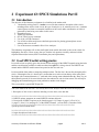
2 Experiment #2: SPICE Simulations Part II
2.1 Introduction:
The objective of this laboratory assignment is to familiarize the student with:
1. Good netlist writing practice. A netlist is a text file that contains a description of the circuit,
including all the sources in the circuit, the type of analysis (ac, dc, transient, noise etc.), simulator
control options to obtain a reasonable simulation of the circuit under consideration. A netlist is
generated by hand using a text editor in this course.
2. Dependent sources
3. Subcircuit command
4. DC/AC/TRAN sweep command
5. Use of the .ALTER command
6. Use of PAR to define and plot user-defined expressions for plotting gain and phase across
arbitrary nodes in a circuit
7. Use of the measure command in WaveView Analyzer.
This laboratory assignment will use the small-signal linear models discussed in class as the vehicle for
highlighting the above. Please ensure that you read the lab questions carefully and turn in all the
requested material (derivations, SPICE simulation plots, and explanations).
2.2 Good SPICE netlist writing practice
It is useful to learn to quickly get to the relevant section and page of the HSPICE manuals using the index
and the search function available in adobe acrobat when a pdf file is being viewed. The HSPICE user
manual and the HSPICE models manual are posted on the class web site.
It is best to think of the netlist as comprising multiple sections. The first line is the one-line description of the
circuit. Following this line, it is best to have a section that serves as the revision history of the netlist. Each
line begins with a comment character (“*”) and ends with a carriage return (obtained when the “Enter” key on
the keyboard is pressed). It is best to include a time, date and time for each revision section. This will help in
debugging and communicating your circuit problems to another circuit designer.
This is a model of a typical SPICE input file.
Title (This must be the first line. It is used by WaveVeiw Analyzer when the results are displayed.)
* Description of the circuit’s function including revision notes, time and date.
***********************************************************************
** HSPICE options statements to control HSPICE simulator behavior
** Description of HSPICE options can be found on page 8-14, Chapter 9, pages 10-22 to 10-36,
** pages 11-24 to 11-26, and page12-7 of the HSPICE manual. (version 2001.4, December 2001).
***********************************************************************
.options post brief nomod alt999
***********************************************************************
** begin description of sub-circuits
***********************************************************************
University of Southern California. EE348L
page4
Lab 2
***********************************************************************
** begin description of top-level circuit netlist
***********************************************************************
***********************************************************************
** begin parameters section
***********************************************************************
***********************************************************************
** begin source section
***********************************************************************
***********************************************************************
** begin analysis section
***********************************************************************
***********************************************************************
** begin Model section
***********************************************************************
***********************************************************************
** begin output form section
***********************************************************************
*Before saving the file, make sure to press return once, and only once, after .END
.END
Note: Remember that SPICE is case insensitive.
2.2.1
Options statements
Options statements (“.options”) are control statements to specify various parameters associated with the
simulator. A description of HSPICE options can be found on page 8-14, Chapter 9, pages 10-22 to 10-36,
pages 11-24 to 11-26, and page12-7 of the HSPICE manual (version 2001.4, December 2001). The
following options are a useful set of options for the beginner.
.options post =1
.options brief
.options nomod
.options alt999
.options accurate
.options acct=1
.options opts
post output data associated with each node in the circuit (page 9-14).
stop printback of netlist until .options brief=0 is encountered (page 9-6).
do not print model decks, which may be large (page 9-9).
generate up to 1000 unique output run files (page 9-5).
useful for accurate simulation of large circuits (page 9-40).
reports job accounting and runtime statistics (page 9-5).
print the current settings of all control options (page 9-10).
Multiple options may be combined on one line. See, for example,
.options post=1 brief nomod alt999 accurate acct=1 opts
2.3 Voltage Controlled Voltage Sources (VCVS)
In Exercise 2 of the laboratory exercises of laboratory #1, we modeled an operational amplifier using a
voltage controlled voltage source (VCVS). These dependent sources are represented in SPICE using the
E element.
University of Southern California. EE348L
page5
Lab 2
The syntax of the E element in SPICE is
Ename n+ n- p+ p- gain <MAX=val> <MIN=val>
Exxx is the name of the E element source, such as E1 or E2. There are four nodes in the dependent
source command. The first two nodes of the voltage controlled voltage source (VCVS), n+ and n-,
represent the node numbers for the positive and negative ports of the output. The second set of node
numbers, in+ and in-, represents the positive and negative nodes of source’s reference voltage.
The gain of the VCVS is indicated by the value of gain. The value of the output is dependent on the
controlling voltage by a factor of the gain.
<MAX=val> and <MIN=val> are optional parameters that determine the maximum and minimum values
the E element can assume during the course of the simulation. In other words, they specify the upper and
lower limits on the voltage the dependent source can assume. These keywords are very useful in modeling
the limits placed by the power supplies on the output voltage of an op-amp.
2.3.1
Examples of VCVS statements:
E1 2 3 1 0 50
In the above example, the output voltage of the VCVS E1, is between nodes 2and 3. The controlling, or
reference voltage is between nodes 1and 0. The gain of the VCVS is 50. Mathematically,
V(2,3)=50*V(1,0). Note that the optional parameters MAX and MIN are absent.
A VCVS can be used to model an op-amp with finite gain and maximum and minimum limits on the
value of the output voltage.
Eopamp1 out+ out- in+ in- 200000.0 MAX=5V MIN=0V
In the above example, Eopamp1 models an op-amp where V(out+,out-)=200000.0*V(in+,in-), with a
maximum voltage of 5.0V and a minimum voltage of 0V.
In many cases, it is useful to parameterize the gain of a VCVS so that simulations that check the
influence of varying gain can be run. This is specified in HSpice as follows:
.param opamp_gain=2e5
Eopamp1 out+ out- in+ in- opamp_gain MAX=5V MIN=0V
In the above example, opamp_gain is a user-defined parameter. It is important to note that user- defined
parameters should not be the same as SPICE commands or reserved keywords. They should also be less
than 16 characters in length. Unpredictable results can occur if user-defined parameters are not different
from SPICE commands or reserved keywords.
University of Southern California. EE348L
page6
Lab 2
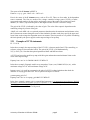
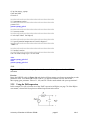
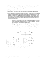
Figure 2-1: (a) VCVS conceptual representation of op-amp, (b) schematic representation.
Conceptually, an ideal op-amp is nothing more than a voltage-controlled voltage source (VCVS) with
infinite gain, infinite input impedance, and zero output impedance as shown in Figure 2-1. The op-amp is
usually represented schematically as a triangle with two input terminals and one output terminal; the internal
VCVS is implied.
Figure 2-2: Behavior of op-amp output voltage, assuming power supply = ±12V.
Practical op-amps have finite, but large gain, with finite, but large input impedances, and finite, but small
output impedances. In addition, the power supplies of the op-amp limit the maximum and minimum
steady-state output voltage that the op-amp can assume. The power supply is limited to a few volts (for
op-amps in the lab, this may be ±12 V, on integrated circuits, perhaps as low as ±1V). The very large
gain is true only for very small inputs signals, and for input voltages greater than a certain value (greater
than 200 µV or less than -200 µV in Figure 2-2), the output simply clips at one of the supply rails,
determined by whether the input signal is positive or negative. This value is determined by the open-loop
gain of the operational amplifier. The SPICE model of the op-amp in Figure 2-1, whose transfer
characteristic is shown in Figure 2-2, is represented below:
E1 out 0 in+ in- 60000.0 MAX=12V MIN=-12V
An input greater than 200 μV results in the output voltage greater than 200 µV x 60000 = 12V, which is
limited by the MAX statement to 12V. Similarly for inputs less than 200 μV, the output voltage falls
below -200 μV x 60000 = -12V and is limited by the MIN statement to –12V.
Revisiting exercise 2 of laboratory assignment #1, we would like to write a SPICE netlist incorporating
University of Southern California. EE348L
page7
Lab 2
good netlist writing principles and the VCVS element we have reviewed so far. In addition, we would
like to add the condition that its power supplies, which are +5V and –5V, limit the output of the op-amp.
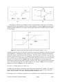
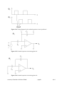
The idealized small-signal model of op-amp is shown in Figure 2-3.
Figure 2-3: Idealized small-signal model of op-amp in Exercise 2 of lab assignment #1.
The model in Figure 2-3 is represented as follows, with in+and in-being the input terminals and out
being the output terminal. The gain of the op-amp is “opamp_gain”.
.param
Rin
Rout
E1
2.3.2
opamp_gain=2e5
in+
in1G
out
vz
1m
vz
0
in+
in-
opamp_gain
MAX=5V
MIN=-5V
Subcircuit representation:
An element like the op-amp can be used many times in a circuit. A hierarchical representation of the
circuit netlist is facilitated by the notion of a subcircuit, which is very similar to the concept of a function
in programming languages. The syntax of the subcircuit, with terminal n1, n2, n3, etc., is shown below
(pages 3-12 to 3-19, HSpice user manual, version 2001.4).
.subckt subcircuit_name
n1 n2 n3 ……
<parameter_name=value>
** subcircuit description
.ends
Very Important Point:_________________________________________________
Note that the subcircuit ends with a “.ends” statement. The optional parameter_name=value
specifies the default value of a parameter specified in the subcircuit description.
The model in Figure 2-3 may be represented as a subcircuit as follows:
.subckt my_opamp in+
Rin
in+
inRout out
A0v
E1
A0v
ref
.ends
in- out ref gain=opamp_gain
1G
1
in+
ingain
MAX=5V
MIN=-5V
A subcircuit is instantiated in a circuit as follows
Xyyy n1 n2 n3 … <parameter_name=value>
University of Southern California. EE348L
page8
Lab 2
Where Xyyy is the name of the subcircuit, n1, n2, n3 etc. are the node names or node numbers of
the particular instantiation of the subcircuit in the top-level circuit. The optional parameter_name=value
sets the value of a parameter in the subcircuit definition for that particular subcircuit instantiation.
The subcircuit, my_opamp is instantiated as follows:
X1 in+ in- out vss my_opamp gain=opamp_gain
Where in+, in-, out, and vss correspond to the terminals in+, in-, out and ref of the subircuit definition of
my_opamp.
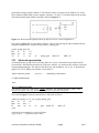
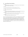
Figure 2-4: Op-amp circuit in Exercise 2 of lab assignment #1.
Using the subcircuit definition called my_opamp, we can write down the SPICE netlist of the op-amp
circuit in Figure 2-4 as follows:
HSPICE netlist of Op-amp circuit in Exercise 2 of lab #1
*Written Jan 24, 2005 for EE348L by Bindu Madhavan.
*Edited July 10, 2012 for EE348L by Aaron Curry
******************************************************
**** options section
******************************************************
.options post=1 brief nomod alt999 accurate acct=1 opts
******************************************************
**** subcircuit section
******************************************************
.subckt my_opamp in+ in- out gain=opamp_gain
Rin in+ in- 1G
Rout out A0v 1m
University of Southern California. EE348L
page9
Lab 2
E1 A0v 0 in+ in- gain MAX=5 MIN=-5
.ends
******************************************************
**** circuit description
******************************************************
rs in inp 50
r1 inp 0 1k
x1 inp inm out my_opamp gain=opamp_gain
rf out inm 100K
r2 inm 0 r2
******************************************************
**** parameters section
******************************************************
.param r2=1k
.param opamp_gain=2e5
******************************************************
**** sources section
******************************************************
v1 in 0 sin(0V 60mV 10x 100ps 0)
******************************************************
**** specify nominal temperature of circuit in degrees C
******************************************************
.TEMP= 27
******************************************************
**** analysis section
******************************************************
.tran 1ns 200ns
.END
Figure 2-5: HSPICE netlist for op-amp circuit in Exercise 2 of lab assignment #1 with supply limit of +/5V for the op-amp.
2.3.3
Parameter sweep in DC/AC/TRAN analysis
In this section, we investigate parameter sweeping in the example netlist shown in Figure 2-5 for the
circuit in Figure 2-4. Our goal is to determine how the transient waveforms in the example netlist
changes as a function of the op-amp gain that we parameterized using the parameter “opamp_gain” in the
subcircuit “my_opamp”. This kind of analysis is called “sweeping a parameter” or “sweeping a variable”.
Although this example is done using a transient analysis, it can be done in both AC and DC analyses as
well.
We change the analysis section in the above example to sweep the parameter r2 through three values:
1k,10k, and 100k. The syntax (page 11-4 (transient sweep) HSpice user manual (version 2001.4)) is as
follows:
.tran resolution duration sweep parameter_name poi number_of_points value1 value2 …..
University of Southern California. EE348L
page10
Lab 2
An example is shown below:
******************************************************
**** analysis section
******************************************************
.tran .1ns 200ns sweep r2 poi 3 1k 10k 100k
Exercise:
Rerun the SPICE netlist in Figure 2-5 with the modification to sweep the parameter r2
through three values of 1k, 10k, 100k. Plot Vo. What should the amplitude for Vo be for each case?
The transient analysis with the parameter sweep will produce multiple waveforms on the same panel in
WaveView Analyzer. To view which waveform corresponds to which parameter value, you can click on
the box next to the waveform name. Then you can separate each waveform by right clicking in the panel
the waveform names are located in.
2.3.4
.ALTER Statements
In HSPICE, embedded sweeps are not allowed. Thus the .ALTER statement can be used so that the same
simulation is repeated for a different value of another parameter. We will practice by changing the
parameter “opamp_gain” using the .ALTER statement (page 3-40 of HSpice user manual, version
2001.4).
An HSpice simulation with n .ALTER statements produces n+1 output files. For a transient analysis of
netlist file mycircuit.spice with 4 .ALTER statements, transient output files mycircuit.tr0,
mycircuit.tr1,….., and mycircuit.tr4 are produced.
Figure 2-6 shows the revised netlist of Figure 2-5 with .ALTER statements. The modified netlist
statements are shown in bold, blue text.
HSPICE netlist of Op-amp circuit in Exercise 2 of lab #1
*Written Jan 24, 2005 for EE348L by Bindu Madhavan.
*Edited July 10, 2012 for EE348L by Aaron Curry.
******************************************************
**** options section
******************************************************
.options post=1 brief nomod alt999 accurate acct=1 opts
******************************************************
**** subcircuit section
******************************************************
. subckt my_opamp in+ in- out gain=opamp_gain
Rin in+ in- 1G
Rout out A0v 1m
E1 A0v 0 in+ in- gain MAX=5 MIN=-5
.ends
******************************************************
**** circuit description
******************************************************
rs in inp 50
r1 inp 0 1k
University of Southern California. EE348L
page11
Lab 2
x1 inp inm out my_opamp
rf out inm 100K
r2 inm 0 r2
******************************************************
**** parameters section
******************************************************
.param r2=1k
.param opamp_gain=1
******************************************************
**** sources section
******************************************************
v1 in 0 sin(0V 60mV 10x 100ps 0)
******************************************************
**** specify nominal temperature of circuit in degrees C
******************************************************
.TEMP= 27
******************************************************
**** analysis section
******************************************************
.tran .1ns 200ns sweep r2 poi 3 1k 10k 100k
.alter
.param opamp_gain=1e2
.alter
.param opamp_gain=1e4
.END
Figure 2-6: HSPICE netlist for op-amp circuit in Exercise 2 of lab assignment #1 with .ALTER
statements
Exercise:
Rerun the HSPICE netlist in Figure 2-6 and plot the different output waveforms corresponding to each
parameter value. You should plot a total of three (3) output waveforms, one for each of the
three opamp_gain parameter values of 1, 100, and 2e5. Do the results match with your expectations?
2.3.5
Using the PAR expression
In this example, we will review the use of the “PAR” expression in HSpice (see page 7-8 of the HSpice
user manual, version 2001.4) to plot user-defined expressions in the netlist.
University of Southern California. EE348L
page12
Lab 2
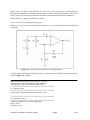
Figure 2-7: First-order RC Low-Pass Filter.
The circuit used in Laboratory 1, exercise 4 is shown in Figure 2-7. The HSPICE netlist for the ac
analysis of Figure 2-7 is shown in Figure 2-8. Parameters rpar1 and cpar1are used in the netlist to
parameterize the value of resistance R and capacitance C in the first-order RC LPF in Figure 2-7. These
parameters are shown in quotes to highlight that expressions within quotes may be used instead of simple
parameters, where each expression involves multiple parameters (see page 7-8 of the HSpice user manual,
version 2001.4).
Analyzing the circuit, we see that the circuit has a pole at ωo=1/RC radians-per-second (rps) =
1/(2πRC) Hz. In a first-order LPF, this is the –3 dB bandwidth of the circuit. The transfer function
of the circuit, Vo(s)/Vin(s), has a phase shift that begins to change from 0 to –45 degrees (=π/4 radians)
at approximately ωo/10 rps, becomes –45 degrees (=π/4 radians) at ωo rps, and –90 degrees at
approximately 10ωo rps.
In order to plot the transfer function and its phase in the .dc, .ac or the .tran analyses, we have to be able
to specify an expression for the transfer function Vo(s)/Vin(s), and the phase shift from input to the
output.
We use the PAR command to do so. The syntax is described on page 7-8 of the HSpice user manual,
version 2001.4. The .probe statement, used to specify the graphical output of node voltages, branch
current and user-defined expressions for a particular analysis is described in page 8-10 of the HSpice user
manual, version 2001.4.
2.3.5.1
Plotting the transfer function
We specify the ac plot of the transfer function = v(out)/v(in), where out and in are the output and input
node names respectively, as follows, where gain is the user-defined plot parameter.
.probe ac gain=par('v(out)/v(in)')
The ac plot of the transfer function, expressed in dB terms is 20*log10(v(out)/v(in)), is:
.probe ac gaindB=par('20*log10(v(out)/v(in))')
In the above expression, log10 is the logarithm to base 10, and gaindB is the user-defined plot parameter.
2.3.5.2 Plotting the phase of the transfer function
The phase of a node voltage or a branch current is specified by using vp(node) or ip(branch_current), as
described on page 8-30 of the HSpice user manual, version 2001.4.
Accordingly, the phase difference from input to the output is
.probe ac phase=par('vp(out)-vp(in)')
where phase is the user-defined plot parameter.
Note: the type of analysis specified in the .probe statements above may be ac, dc, noise or tran,
permitting the graphical display of user-defined expression in ac analysis, dc analysis, noise analysis and
transient analysis.
SPICE netlist of circuit to demonstrate parameter sweep in ac analysis
*Written Jan 24, 2005 for EE348L by Bindu Madhavan.
*Edited July 10, 2012 for EE348L by Aaron Curry.
******************************************************
**** options section
University of Southern California. EE348L
page13
Lab 2
******************************************************
.options post=1 brief nomod alt999 accurate acct=1 opts
******************************************************
**** circuit description
******************************************************
R1 in out ‘rpar1’
C1 out 0 ‘cpar1’
******************************************************
**** parameters section
******************************************************
.param rpar1=1k
.param cpar1=10pF
******************************************************
**** sources section
******************************************************
v1 in 0 ac 1
******************************************************
**** probe statement section
******************************************************
.probe ac gain=par('v(out)/v(in)')
.probe ac gaindB=par('20*log10(v(out)/v(in))')
.probe ac phase=par('vp(out)-vp(in)')
******************************************************
**** specify nominal temperature of circuit in degrees C
******************************************************
.TEMP=27
******************************************************
**** analysis section
******************************************************
.ac dec 100 10k 10G sweep rpar1 poi 3 100 1e3 1e4
.alter
.param cpar1=100pF
.END
Figure 2-8: HSPICE netlist highlighting ac analysis with parameter variation and user-defined expression
2.3.5.6
Printing from HSPICE
See Laboratory Experiment 1, section 1.9.3 for printing with WaveView Analyzer.
Another method is to use ctrl+PrintScreen while a window containing the plot is open on your desktop.
Then the entire window can be pasted (and edited before submitting).
2.4 Voltage Controlled Current Sources (VCCS)
University of Southern California. EE348L
page14
Lab 2
Voltage Controlled Current Sources (VCCS) are dependent sources that are represented in HSpice using
the G element (page 5-34 of the HSpice user manual, version 2001.4). The G element can also be used to
describe a Voltage Controlled Resistor (VCR) or a switch (page 5-35 of the HSpice user manual, version
2001.4).
The syntax of the G element in HSpice is
Gxxx n+ n- in+ in- <MAX=val> <MIN=val> transconductance
Gxxx is the name of the G element source, such as G1 or G2. There are four nodes in the dependent
source command. The first two nodes of the voltage controlled current source (VCCS), n+ and n-,
represent the node numbers for the positive and negative ports of the output. The second set of node
numbers, in+ and in-, represents the positive and negative nodes of source’s reference voltage.
<MAX=val> and <MIN=val> are optional parameters that determine the maximum and minimum
values the G element can assume during the course of the simulation. In other words, they specify the
upper and lower limits on the current the dependent source can assume. These keywords are very useful
in modeling the limits placed by the power supplies on the output current of the device.
The gain of the VCCS is indicated by the value of transconductance. The value of the output
is dependent on the controlling voltage by a factor of the transcondutance.
2.4.1 Examples of VCCS statements
G1 2 3 1 0 50
In the above example, the output current of the VCCS G1, is between nodes 2 and 3. The
controlling, or reference voltage is between nodes 1 and 0. The gain of the VCVS is 50.
Mathematically, I(2,3)=50 xV(1,0). Note that optional parameter MAX and MIN are absent.
A VCCS can be used to model a device, such as a MOSFET, with finite transconductance and
maximum and minimum limits on the value of the output current.
GMOSFET1 out+ out- in+ in- MAX=5e-6A MIN=0A 200000.0
In the above example, GMOSFET1 models a MOSFET where I(out+,out-)=200000.0xV(in+,in-), with a
maximum current of 5e-6A and a minimum current of 0A.
The G element can also be used as a switch by making it a Voltage Controlled Resistor (VCR):
Gswitch 2 0 VCR PWL(1) 1 0 0v,10meg 1v,1m
The resistance between nodes 2 and 0 varies linearly from 10 meg to 1 m ohms when voltage across
nodes 1 and 0 varies between 0 and 1 volt. Beyond the voltage limits, the resistance remains at 10 meg
and 1 m ohms, respectively.
In many cases, it is useful to parameterize the transconductance of a VCCS so that simulations
that check the influence of varying transconductance can be run. This is specified in HSpice as
follows:
.param transconductance=2e5
GMOSFET1 out+ out- in+ in- MAX=5e-6A MIN=0A transconductance
University of Southern California. EE348L
page15
Lab 2
In the above example, transconductance is a user-defined parameter. It is important to note that
user-defined parameters should not be the same as HSpice commands or reserved keywords.
They should also be less than 16 characters in length. Unpredictable results can occur if user defined
parameters are not different from HSpice commands or reserved keywords. See Chapter 7 of the HSpice
user manual, version 2001.4, “Parameters and Functions.”
2.5 Current Controlled Current Sources (CCCS)
Current Controlled Current Sources (CCCS) are dependent sources that are represented in HSpice using
the F element (page 5-46 of the HSpice user manual, version 2001.4). In order to specify a currentcontrolled dependent source, we have to be able to specify the controlling current. This is done in HSpice
by using a voltage source of 0V to measure the controlling current.
The syntax of the F element in HSpice is
Fxxx n+ n- vsens <MAX=val> <MIN=val> currentgain
Fxxx is the name of the F element source, such as F1 or F2. There are two nodes in the dependent source
command. The two nodes of the current controlled current source (CCCS), n+ and n-, represent the node
numbers for the positive and negative ports of the output current source. The parameter vsens represents
the name of the voltage source element through which the controlling current flows.
<MAX=val> and <MIN=val> are optional parameters that determine the maximum and minimum values
of output current the F element can assume during the course of the simulation. In other words, they
specify the upper and lower limits on the current the dependent source can assume. These keywords are
very useful in modeling the limits placed on the output current.
The gain of the CCCS is indicated by the value of currentgain. The value of the output is dependent on
the controlling voltage by a factor of the currentgain. The mathematical representation of the CCCS is
I(n+,n-) = currentgain x current flowing through vsens = currentgain x I(vsens)
2.5.1 Examples of CCCS statements
F1 2 3 V1 50
In the above example, the output current of the CCCS F1, is between nodes 2 and 3. The controlling, or
reference current is flowing through voltage source V1 in the circuit. The current gain of the CCCS is 50.
Mathematically, I(2,3)=50 xI(V1). Note that optional parameter MAX and MIN are absent.
A CCCS can be used to model a device with finite gain and maximum and minimum limits on the value
of the output voltage.
Flimited out+ out- V1 MAX=5A MIN=0A 1000
In the above example, Flimited models a device where I(out+,out-)=1000.0 xI(V1), with a maximum
current of 5.0A and a minimum current of 0A.
In many cases, it is useful to parameterize the currentgain of a CCCS so that simulations that check the
influence of varying currentgain can be run. This is specified in HSpice as follows:
University of Southern California. EE348L
page16
Lab 2
.param currentgain=2e5
Flimited out+ out- V1 MAX=5A MIN=0A currentgain
In the above example, currentgain is a user-defined parameter. It is important to note that
user-defined parameters should not be the same as HSpice commands or reserved keywords.
They should also be less than 16 characters in length. Unpredictable results can occur if user defined
parameters are not different from HSpice commands or reserved keywords. See Chapter 7 of the HSpice
user manual, version 2001.4, “Parameters and Functions.”
2.6 Current Controlled Voltage Sources (CCVS)
Current Controlled Voltage Sources (CCVS) are dependent sources that are represented in SPICE using
the H element (page 5-42 of the HSpice user manual, version 2001.4). In order to specify a currentcontrolled dependent source, we have to be able to specify the controlling current. This is done in
SPICE by using a voltage source of 0V to measure the controlling current.
The syntax of the H element in SPICE is
Hxxx n+ n- vsens transresistance <MAX=val> <MIN=val>
Hxxx is the name of the H element source, such as H1 or H2. There are two nodes in the
dependent source command. The two nodes of the current controlled voltage source (CCVS), n+ and n-,
represent the node numbers for the positive and negative ports of the output. The parameter vsens
represents the name of the voltage source element through which the controlling current flows.
The gain of the CCVS is indicated by the value of transresistance. The value of the output is dependent on
the controlling voltage by a factor of the transresistance. The mathematical representation of the CCVS is
V(n+,n-) = transresistance*current flowing through vname
2.6.1
Examples of CCVS statements
H1 2 3 V1 50
In the above example, the output voltage of the CCVS H1, is between nodes 2and 3. The controlling, or
reference current is flowing through voltage source V1 in the circuit. The gain of the CCVS is 50.
Mathematically, V(2,3)=50*I(V1). Note that optional parameter MAX and MIN are absent.
A CCVS can be used to model a device with finite gain and maximum and minimum limits on the value
of the output voltage.
Hlimited out+ out- V1 MAX=5V MIN=0V 1000
In the above example, Hlimited models a device where V(out+,out-)=1000.0 �I(V1), with a maximum
voltage of 5.0V and a minimum voltage of 0V.
In many cases, it is useful to parameterize the transresistance of a CCVS so that simulations that check
the influence of varying transresistance can be run. This is specified in HSpice as follows:
.param transres=2e5
Hlimited out+ out- V1 MAX=5V MIN=0V transres
In the above example, transres is a user-defined parameter. It is important to note that user- defined
University of Southern California. EE348L
page17
Lab 2
parameters should not be the same as SPICE commands or reserved keywords. They should also be less
than 16 characters in length. Unpredictable results can occur if user-defined parameters are not different
from SPICE commands or reserved keywords.
Of all the dependent sources, the CCVS is the least encountered source you
will find. The other three sources are encountered by the listed elements:
VCVS: Op-Amp
VCCS: MOSFET
CCCS: BJT
2.7 References
[1]
HSPICE user manual posted on EE348L class web site.
[3]
EE348L Laboratory Experiment 1, Spring 2005, posted on EE348L class web site.
[4]
J. Choma, EE348L Lecture Supplement 1.
University of Southern California. EE348L
page18
Lab 2
2.8 Lab Exercises
Note:
•
•
•
In your lab report, include a clean printout of the SPICE netlist for each Lab
question and its parts.
Take care that you do not make typographical errors, as this can result in
erroneous results and increase your debugging time. Ensure that you use the
correct dependent source. Refer to section 1.9 of laboratory assignment 1, “HSPICE
Guidelines Review” to refresh up on the HSPICE Guidelines.
When doing an .AC sweep, make sure the horizontal axis (frequency) is logarithmic!
1)
Perform the exercise in Section 2.3.3, “Parameter sweep in DC/AC/TRAN analysis”.
C a l c u l a t e t h e g a i n f o r t h e s e t h r e e r e s i s t a n c e v a l u e s . Justify that the results of the
transient analysis simulations for the three r2 values of 1k, 10k, and 100k agree with your calculations
by including a cursor. Submit the plot of the transient analysis.
2)
Perform the exercise in section 2.3.4 “.ALTER Statements” using the netlist in Figure 3-6.
Submit a plot of the transient analysis results with the transient analysis for each value of parameter
opamp_gain in a separate panel, and all panels in the same window.
3)
Use the netlist in Figure 2-8, section 2.3.5, “AC sweep example”, plot the user-defined
gaindB and phase plot parameters on separate panels on the same page for cpar1=100pF and
rpar1 values of 100, 1000 and 10000 ohms.
A) What should the -3db frequency be for each rpar1 value?
B) What should the phase at the -3db frequency be?
C) Measure the –3 dB frequency of each LPF and the value of the phase of the transfer function
of the circuit at the –3 dB frequency of each LPF. Do your simulations agree with your hand
calculations?
4)
Recall the circuit used from lab 1 exercise 2 with an added feedback capacitor:
University of Southern California. EE348L
page19
Lab 2
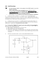
Figure 2-9: Feedback amplifier circuit schematic for problem 4.
A) Determine the new transfer function.
i.
How does the addition of Cf alter the transfer function? (Let R1>>Rs and
Ao>>Ai.)
ii.
What is the low frequency gain in dB?
iii.
What is the high frequency gain in dB?
iv.
What is the time constant associated with pole caused by Cf?
v.
What is the time constant associated with the zero caused by Cf?
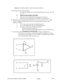
B) Model the op-amp using the models shown below. Let Vcc=Vee=10V. Let Ao=80dB
(100e6). Perform a transient analysis with Vs having amplitude of 100mV, and a
frequency of 1MHz.
i.
If we want to plot 10 periods, what should tstop be?
ii.
If we want 100 points per period, what should tstep be?
iii.
Attempt to plot the gain by using the following:
.probe tran gain=par(‘v(out)/v(s)’)
What is the problem with plotting the gain this way? Hint: What vale
does the input equal periodically?
C) Now, plot the gain by performing an .AC sweep with Vs having a magnitude of 1.
i. If we want to sweep within 3 decades before and after frequencies of interest,
what frequency range should we sweep? (NOTE: you should sweep 3 decades
before the pole and 3 decades after the zero.)
Figure 2-10: A regular 741 op-amp
Figure 2-11: Equivalent circuit model of an op-amp
University of Southern California. EE348L
page20
Lab 2
5)
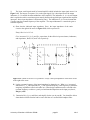
The linear, small-signal model of a tuned amplifier which includes the input signal source is in
Figure 2-12. The output, or response (Vo), to the input signal (Vs) is developed across the output
inductance Lo. Gm models the transconductance of the amplifier. The inductance Ls is a circuit element
that is exploited to achieve maximum power transfer between the applied input signal and the amplifier
input port, whose input impedance is delineated as Zin(s). The inductance Lg is a circuit element that
is used to tune the resonant frequency of the amplifier. The output inductance Lo controls the gain at
resonant frequency.
A) Show that the indicated input impedance, Zin(s), the input impedance of the entire
circuit to the right of the arrow in Figure 2-12, can be expressed as
Zin(s)=Reff+Leff*s+1/Ceff*s
Give, in terms of Cin, Ls, Lg and Gm, expressions for the effective input resistance, inductance,
and capacitance, Reff, Leff, and Ceff, respectively.
Figure 2-12: Tuned circuit for VCCS problem 5. Zin(s) is the input impedance of the entire circuit
to the right of the arrow.
B) Let the resonant frequency of the input impedance be denoted as ωo. What is ωo in terms of
inductances Ls, Lg and capacitance Cin? (The resonant frequency is the frequency at which the
imaginary impedances cancel each other out.) What design condition must be satisfied at the
resonant frequency to achieve a purely real and matched impedance at the input port; that is,
Zin(jωo) ≡ Rs?
C) Determine H(s), Q, ωo, and H(ωo) and simplify for the case in part (B). You should be able to
show that the transfer function can be cast in the form of a second order bandpass filter:
University of Southern California. EE348L
page21
Lab 2
s
Qwo
H ( s) H ( wo )
s
s
1
Qwo wo
2
What is the low frequency gain? What is the high frequency gain? What is the phase at resonant
frequency in degrees?
D) Model the amplifier in Figure 2-12 in SPICE, using the SPICE Voltage Controlled Current
Source (VCCS) element, G. Represent the core element of the amplifier, as outlined by the
dotted-line box in Figure 2-12, as a sub-circuit in your netlist. Let Gm=2.5mmho, Rs=50 Ohms,
Cin=50fF, Lo=5nH, and Ls=1nH. Let Lg be a parameter with default value of 1nH.
a. Perform an ac-sweep from 100 MHz to 1THz, varying the value of Lg over three (3)
values: 1nH, 5nH, 10nH. Plot gaindB, phase, zin, and pin (input power) versus frequency
on a logarithmic scale on separate panels. As we alter Lg, which plots should change
(refer to your answers in part (C))? How should they change? D o y o u r s i m u l a t i o n s
agree with your responses? Make sure you zoom in on the Rin
vertical axis so that the max value is 500Ω.
b. Calculate the values of the resonant frequency, gain (dB) at resonant frequency, phase at
resonant frequency, zin at resonant frequency, and pin at resonant frequency for the
default values (the sweeps with Ls=Lg=1nH). Verify these values in HSpice with a cursor
on your sweep.
NOTE: zin and pin can be calculated as:
.probe ac zin=par(‘v(vs)/i(vs)-rs’)
.probe ac pin=par(‘v(inpAmp)*i(vs)’)
Where vs is an AC source named vs between nodes vs and 0, and rs is a parameter that defines the value
for Rs. You should know that these are complex values whose magnitudes will be plotted. Zin and Pin
are only real at resonant frequency.
As shown below, use a 1000 point decade sweep for the ac analysis.
.ac dec 1000 100MEG 1T
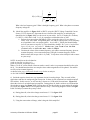
6) Switched capacitor circuits are very important circuits for analog design. They are used in filter
applications and also for analog-to-digital conversion. In these circuits, transistors are turned on and off
like switches. In this exercise, we will use the G element as a VCR model for transistors. Figure 2-13
shows the circuit of a switched capacitor amplifier. During phase Φ1, the Φ1 switches are closed and the
Φ2 switches are open (See Figure 2-15). During phase Φ2, the Φ1 switches are open and the Φ2 switches
are closed (See Figure 2-16). The two phases do not overlap. Their timing diagram is shown in Figure
2-14. For analysis, assume the op-amp is ideal.
A) During phase Φ1, what is the charge stored across C1? Use figure 2-15.
B) During phase Φ2, what is the charge stored across C2? Use figure 2-16.
C) Using the conservation of charge, what is the gain of this amplifier?
University of Southern California. EE348L
page22
Lab 2
D) During phase Φ2, the current in C1 flows to ground to the left to discharge the capacitor. This
current flows through capacitor C2 in the same direction. At the end of Φ2, is Vo positive or
negative? Is this an inverting or non-inverting amplifier?
E) During phase Φ1, what does Vo equal?
F) During phase Φ2, what does Vo equal? Note: this value is sampled at the end of phase Φ1!
G) Verify your answers by simulating the circuit using HSPICE. Use the model of an op-amp from
problem 4. Perform a transient analysis with Vs being a SIN wave with amplitude of 1V and a
frequency of 10MHz. Let Φ1 and Φ2 be pulses with periods of 1ns, ‘on’ times of .4ns, and rise
and fall times of 1ps. Use voltage controlled resistors to model the switches with impedances
going from 1MΩ to .1mΩ in the ‘off’ and ‘on’ states respectively. Let C2=1pF and C1=5pF.
Let tstep=1n and tstop=201n.
a. If we want Φ1 to have a delay of 1ns, what should the delay of Φ2 be? We want no
overlap and maximum separation between the on states of each phase. What is the
gain of this circuit? What amplitude should Vo have?
b. Plot Vint and Vout in separate panels. Does Vint look like you expect? What about
Vout? What happens to Vout in between Φ2 opening up and Φ1 closing? Why? Now
you can see why it is important to have a ‘reset’ on the output voltage. It is also
important that your output is able to settle to the desired value before Φ2 opens!
Figure 2-13: A switched capacitor amplifier for problem 6.
University of Southern California. EE348L
page23
Lab 2
Figure 2-14: Timing diagram for the switched capacitor circuit in problem 6.
Figure 2-15: Switched capacitor circuit during phase Φ1.
Figure 2-16: Switched capacitor circuit during phase Φ2.
University of Southern California. EE348L
page24
Lab 2
2.9
General Report Format Guidelines
1. Introduction
Explain what the lab is about. Describe the circuits being built in terms of structure and purpose.
Also talk about what is being investigated.
2. Procedure
Step by step talk about what was done and show diagrams of the circuits.
3. Data
Present all data taken during the lab. It should be organized and easy to read.
4. Questions
Answer all the questions in the lab.
5. Discussion
Discuss the results you obtained. What significance is there in the results? How do they help your
investigation? Explain the meaning; the numbers alone aren’t good enough.
6. Conclusion
Wrap up the report by giving some comments on the lab. Do the results clearly agree with what
the lab was trying to teach? Did you have any problems? Suggestions?
7. Attachments
Attach all hand calculations and SPICE plots necessary.
NOTE: You are turning in lab reports that are to be graded. If you want good marks, be sure to make the
reports as neat and aesthetically appealing as possible. If you refer to an attached plot, include the page
number. If you refer to a hand calculation, be sure to highlight what you are referring to on the page
containing the hand calculation. However, including equations, plots, figures, etc. in the body of your
report is good practice. Be sure to include plot titles. Be sure to include axis titles and units. Lab reports
are to be typed. HANDWRITTEN REPORTS WILL NOT BE ACCEPTED. LAB REPORTS ARE
DUE AT THE BEGINNING OF THE NEXT LAB. THEY WILL NOT BE ACCEPTED IF THEY ARE
MORE THAN 15 MINUTES LATE!
University of Southern California. EE348L
page25
Lab 2