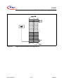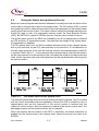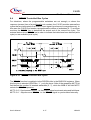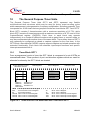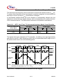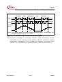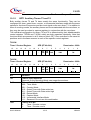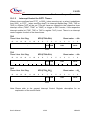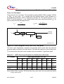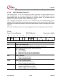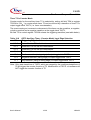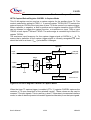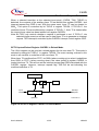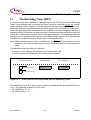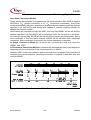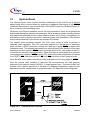
1
www.infineon.com
Microcontrollers
C166 Family
16-Bit Single-Chip Microcontroller
C161PI
User’s Manual 1999-08
V 1.0
Ausgabe 1999-08
Herausgegeben von
Infineon Technologies AG,
St.-Martin-Strasse 53
D-81541 München
© Infineon Technologies AG 1999.
Alle Rechte vorbehalten.
Edition 1999-08
Published by
Infineon Technologies AG,
St.-Martin-Strasse 53
D-81541 München
© Infineon Technologies AG 1999.
All Rights Reserved.
Wichtige Hinweise!
Mit den Angaben werden die Bauelemente
spezifiziert, nicht Eigenschaften zugesichert.
Liefermöglichkeiten und technische Änderungen sind vorbehalten.
Für die angegebenen Schaltungen, Beschreibungen und Tabellen wird keine Gewähr bezüglich der Freiheit von Rechten
Dritter oder deren Richtigkeit übernommen.
Infineon Technologies ist ein Hersteller von
CECC-qualifizierten Produkten.
Attention please!
The information herein is given to describe
certain components and shall not be considered as warranted characteristics.
Terms of delivery and rights to technical
change reserved.
We hereby disclaim any and all warranties,
including but not limited to warranties of
non-infringement, regarding circuits, descriptions and charts stated herein.
Infineon Technologies is an approved
CECC manufacturer.
Auskünfte
Fragen über Technik, Preise, Liefermöglichkeiten und -bedingungen richten Sie
bitte an den Ihnen nächstgelegenen Vertrieb Infineon Technologies in Deutschland
oder an unsere Vertriebsstellen im Ausland.
Information
For further information on technology, delivery terms and conditions and prices
please contact your nearest Infineon Technologies Office in Germany or our Infineon
Technologies Representatives worldwide
(see address list).
Warnhinweise
Bauelemente können aufgrund technischer Erfordernisse Gefahrstoffe enthalten. Auskünfte darüber bitten wir unter Angabe des betreffenden Typs ebenfalls über
den Vertrieb Infineon Technologies einzuholen.
Infineon Technologies Bauelemente dürfen
nur mit ausdrücklicher schriftlicher Genehmigung von Infineon Technologies in lebenserhaltenden Geräten oder Systemen
eingesetzt werden, falls beim Ausfall des
Bauelementes berechtigter Grund zur Annahme besteht, daß das lebenserhaltende
Gerät oder System ausfällt bzw. dessen Sicherheit oder Wirksamkeit beeinträchtigt
wird. Lebenserhaltende Geräte und Systeme sind zur chirurgischen Einpflanzung in
den menschlichen Körper gedacht oder
unterstützen bzw. erhalten das menschliche Leben. Sollten sie ausfallen, besteht
berechtigter Grund zur Annahme, daß die
Gesundheit des Anwenders gefährdet werden kann.
Warnings
Due to technical requirements components
may contain dangerous substances. For information on the types in question please
contact your nearest Infineon Technologies
Office.
Infineon Technologies Components may
only be used in life-support devices or systems with the express written approval of
Infineon Technologies, if a failure of such
components can reasonably be expected
to cause the failure of that life-support device or system, or to affect the safety or effectiveness of that device or system. Life
support devices or systems are intended to
be implanted in the human body, or to support and/or maintain and sustain and/or
protect human life. If they fail, it is reasonable to assume that the health of the user
or other persons may be endangered.
Microcontrollers
C166 Family
16-Bit Single-Chip Microcontroller
C161PI
V 1.0,
1999-08
User’s Manual
C161PI
Revision History:
1999-08 (V 1.0)
Previous Versions:
User’s Manual C161RI, 05.98 (V 1.0)
Page
Subjects (major changes since last revision)
We Listen to Your Comments
Any information within this document that you feel is wrong, unclear or missing at all?
Your feedback will help us to continuously improve the quality of this document.
Please send your proposal (including a reference to this document) to:
[email protected]
The C161PI is the successor of the C161RI. Therefore this manual also replaces the C161RI
manual.
C161PI
Table of Contents
Page
1
1.1
1.2
1.3
Introduction . . . . . . . . . . . . . . . . . . . . . . . . . . . . . . . . . . . . . . . . . . . . . . . 1-1
The Members of the 16-bit Microcontroller Family . . . . . . . . . . . . . . . . . . 1-2
Summary of Basic Features . . . . . . . . . . . . . . . . . . . . . . . . . . . . . . . . . . . 1-4
Abbreviations . . . . . . . . . . . . . . . . . . . . . . . . . . . . . . . . . . . . . . . . . . . . . . 1-7
2
2.1
2.1.1
2.1.2
2.2
2.3
2.4
2.5
Architectural Overview . . . . . . . . . . . . . . . . . . . . . . . . . . . . . . . . . . . . . . 2-1
Basic CPU Concepts and Optimizations . . . . . . . . . . . . . . . . . . . . . . . . . 2-2
High Instruction Bandwidth / Fast Execution . . . . . . . . . . . . . . . . . . . . . 2-3
Programmable Multiple Priority Interrupt System . . . . . . . . . . . . . . . . . 2-7
The On-chip System Resources . . . . . . . . . . . . . . . . . . . . . . . . . . . . . . . . 2-8
The On-chip Peripheral Blocks . . . . . . . . . . . . . . . . . . . . . . . . . . . . . . . 2-11
Power Management Features . . . . . . . . . . . . . . . . . . . . . . . . . . . . . . . . 2-18
Protected Bits . . . . . . . . . . . . . . . . . . . . . . . . . . . . . . . . . . . . . . . . . . . . . 2-20
3
3.1
3.2
3.3
3.4
3.5
Memory Organization . . . . . . . . . . . . . . . . . . . . . . . . . . . . . . . . . . . . . . . 3-1
Internal ROM Area . . . . . . . . . . . . . . . . . . . . . . . . . . . . . . . . . . . . . . . . . . 3-3
Internal RAM and SFR Area . . . . . . . . . . . . . . . . . . . . . . . . . . . . . . . . . . 3-4
The On-Chip XRAM . . . . . . . . . . . . . . . . . . . . . . . . . . . . . . . . . . . . . . . . . 3-9
External Memory Space . . . . . . . . . . . . . . . . . . . . . . . . . . . . . . . . . . . . 3-11
Crossing Memory Boundaries . . . . . . . . . . . . . . . . . . . . . . . . . . . . . . . . 3-12
4
4.1
4.2
4.3
4.4
4.5
The Central Processing Unit (CPU) . . . . . . . . . . . . . . . . . . . . . . . . . . . . 4-1
Instruction Pipelining . . . . . . . . . . . . . . . . . . . . . . . . . . . . . . . . . . . . . . . . . 4-4
Particular Pipeline Effects . . . . . . . . . . . . . . . . . . . . . . . . . . . . . . . . . . . . 4-7
Bit-Handling and Bit-Protection . . . . . . . . . . . . . . . . . . . . . . . . . . . . . . . 4-11
Instruction State Times . . . . . . . . . . . . . . . . . . . . . . . . . . . . . . . . . . . . . 4-12
CPU Special Function Registers . . . . . . . . . . . . . . . . . . . . . . . . . . . . . . . 4-13
5
5.1
5.1.1
5.2
5.3
5.4
5.5
5.6
5.7
5.8
5.9
Interrupt and Trap Functions . . . . . . . . . . . . . . . . . . . . . . . . . . . . . . . . . 5-1
Interrupt System Structure . . . . . . . . . . . . . . . . . . . . . . . . . . . . . . . . . . . . 5-2
Interrupt Control Registers . . . . . . . . . . . . . . . . . . . . . . . . . . . . . . . . . . . 5-5
Operation of the PEC Channels . . . . . . . . . . . . . . . . . . . . . . . . . . . . . . 5-11
Prioritization of Interrupt and PEC Service Requests . . . . . . . . . . . . . . . 5-15
Saving the Status during Interrupt Service . . . . . . . . . . . . . . . . . . . . . . . 5-17
Interrupt Response Times . . . . . . . . . . . . . . . . . . . . . . . . . . . . . . . . . . . 5-18
PEC Response Times . . . . . . . . . . . . . . . . . . . . . . . . . . . . . . . . . . . . . . 5-21
Interrupt Node Sharing . . . . . . . . . . . . . . . . . . . . . . . . . . . . . . . . . . . . . 5-23
External Interrupts . . . . . . . . . . . . . . . . . . . . . . . . . . . . . . . . . . . . . . . . . 5-24
Trap Functions . . . . . . . . . . . . . . . . . . . . . . . . . . . . . . . . . . . . . . . . . . . . 5-29
6
6.1
6.2
6.3
Clock Generation . . . . . . . . . . . . . . . . . . . . . . . . . . . . . . . . . . . . . . . . . . . 6-1
Oscillator . . . . . . . . . . . . . . . . . . . . . . . . . . . . . . . . . . . . . . . . . . . . . . . . . . 6-2
Frequency Control . . . . . . . . . . . . . . . . . . . . . . . . . . . . . . . . . . . . . . . . . . . 6-4
Oscillator Watchdog . . . . . . . . . . . . . . . . . . . . . . . . . . . . . . . . . . . . . . . . . 6-8
User’s Manual
-1
1999-08
C161PI
Table of Contents
Page
6.4
Clock Drivers . . . . . . . . . . . . . . . . . . . . . . . . . . . . . . . . . . . . . . . . . . . . . . . 6-9
7
7.1
7.2
7.3
7.4
7.5
7.6
7.7
7.8
7.9
7.10
Parallel Ports . . . . . . . . . . . . . . . . . . . . . . . . . . . . . . . . . . . . . . . . . . . . . . 7-1
Input Threshold Control . . . . . . . . . . . . . . . . . . . . . . . . . . . . . . . . . . . . . . 7-2
Output Driver Control . . . . . . . . . . . . . . . . . . . . . . . . . . . . . . . . . . . . . . . . . 7-4
Alternate Port Functions . . . . . . . . . . . . . . . . . . . . . . . . . . . . . . . . . . . . . 7-7
PORT0 . . . . . . . . . . . . . . . . . . . . . . . . . . . . . . . . . . . . . . . . . . . . . . . . . . . . 7-9
PORT1 . . . . . . . . . . . . . . . . . . . . . . . . . . . . . . . . . . . . . . . . . . . . . . . . . . . 7-13
Port 2 . . . . . . . . . . . . . . . . . . . . . . . . . . . . . . . . . . . . . . . . . . . . . . . . . . . . 7-16
Port 3 . . . . . . . . . . . . . . . . . . . . . . . . . . . . . . . . . . . . . . . . . . . . . . . . . . . . 7-19
Port 4 . . . . . . . . . . . . . . . . . . . . . . . . . . . . . . . . . . . . . . . . . . . . . . . . . . . . 7-24
Port 5 . . . . . . . . . . . . . . . . . . . . . . . . . . . . . . . . . . . . . . . . . . . . . . . . . . . . 7-27
Port 6 . . . . . . . . . . . . . . . . . . . . . . . . . . . . . . . . . . . . . . . . . . . . . . . . . . . . 7-30
8
Dedicated Pins . . . . . . . . . . . . . . . . . . . . . . . . . . . . . . . . . . . . . . . . . . . . 8-1
9
9.1
9.2
9.3
9.4
9.5
9.6
9.7
The External Bus Interface . . . . . . . . . . . . . . . . . . . . . . . . . . . . . . . . . . 9-1
Single Chip Mode . . . . . . . . . . . . . . . . . . . . . . . . . . . . . . . . . . . . . . . . . . 9-2
External Bus Modes
. . . . . . . . . . . . . . . . . . . . . . . . . . . . . . . . . . . . . . . 9-3
Programmable Bus Characteristics . . . . . . . . . . . . . . . . . . . . . . . . . . . . 9-12
READY Controlled Bus Cycles . . . . . . . . . . . . . . . . . . . . . . . . . . . . . . . 9-17
Controlling the External Bus Controller . . . . . . . . . . . . . . . . . . . . . . . . . . 9-19
EBC Idle State . . . . . . . . . . . . . . . . . . . . . . . . . . . . . . . . . . . . . . . . . . . . 9-27
The XBUS Interface . . . . . . . . . . . . . . . . . . . . . . . . . . . . . . . . . . . . . . . . 9-28
10
10.1
10.1.1
10.1.2
10.1.3
10.2
10.2.1
10.2.2
10.2.3
The General Purpose Timer Units . . . . . . . . . . . . . . . . . . . . . . . . . . . . 10-1
Timer Block GPT1 . . . . . . . . . . . . . . . . . . . . . . . . . . . . . . . . . . . . . . . . . 10-1
GPT1 Core Timer T3 . . . . . . . . . . . . . . . . . . . . . . . . . . . . . . . . . . . . . 10-3
GPT1 Auxiliary Timers T2 and T4 . . . . . . . . . . . . . . . . . . . . . . . . . . 10-13
Interrupt Control for GPT1 Timers . . . . . . . . . . . . . . . . . . . . . . . . . . . 10-22
Timer Block GPT2 . . . . . . . . . . . . . . . . . . . . . . . . . . . . . . . . . . . . . . . . 10-23
GPT2 Core Timer T6 . . . . . . . . . . . . . . . . . . . . . . . . . . . . . . . . . . . . 10-25
GPT2 Auxiliary Timer T5 . . . . . . . . . . . . . . . . . . . . . . . . . . . . . . . . . 10-28
Interrupt Control for GPT2 Timers and CAPREL . . . . . . . . . . . . . . . . 10-36
11
11.1
11.2
11.3
11.4
11.5
The Asynchronous/Synchronous Serial Interface . . . . . . . . . . . . . . 11-1
Asynchronous Operation . . . . . . . . . . . . . . . . . . . . . . . . . . . . . . . . . . . . 11-5
Synchronous Operation . . . . . . . . . . . . . . . . . . . . . . . . . . . . . . . . . . . . . 11-8
Hardware Error Detection Capabilities . . . . . . . . . . . . . . . . . . . . . . . . . 11-10
ASC0 Baud Rate Generation . . . . . . . . . . . . . . . . . . . . . . . . . . . . . . . . 11-11
ASC0 Interrupt Control . . . . . . . . . . . . . . . . . . . . . . . . . . . . . . . . . . . . 11-15
12
12.1
12.2
The High-Speed Synchronous Serial Interface . . . . . . . . . . . . . . . . . 12-1
Full-Duplex Operation . . . . . . . . . . . . . . . . . . . . . . . . . . . . . . . . . . . . . . 12-7
Half Duplex Operation . . . . . . . . . . . . . . . . . . . . . . . . . . . . . . . . . . . . . 12-10
User’s Manual
-2
1999-08
C161PI
Table of Contents
Page
12.3
12.4
12.5
12.6
12.7
Continuous Transfers . . . . . . . . . . . . . . . . . . . . . . . . . . . . . . . . . . . . . . 12-11
Port Control . . . . . . . . . . . . . . . . . . . . . . . . . . . . . . . . . . . . . . . . . . . . . . 12-12
Baud Rate Generation . . . . . . . . . . . . . . . . . . . . . . . . . . . . . . . . . . . . . 12-13
Error Detection Mechanisms . . . . . . . . . . . . . . . . . . . . . . . . . . . . . . . . 12-14
SSC Interrupt Control . . . . . . . . . . . . . . . . . . . . . . . . . . . . . . . . . . . . . . 12-16
13
13.1
13.2
The Watchdog Timer (WDT) . . . . . . . . . . . . . . . . . . . . . . . . . . . . . . . . 13-1
Operation of the Watchdog Timer . . . . . . . . . . . . . . . . . . . . . . . . . . . . . . 13-3
Reset Source Indication . . . . . . . . . . . . . . . . . . . . . . . . . . . . . . . . . . . . . 13-6
14
The Real Time Clock
15
The Bootstrap Loader
16
16.1
16.2
16.3
The Analog / Digital Converter . . . . . . . . . . . . . . . . . . . . . . . . . . . . . . 16-1
Mode Selection and Operation . . . . . . . . . . . . . . . . . . . . . . . . . . . . . . . . 16-2
Conversion Timing Control . . . . . . . . . . . . . . . . . . . . . . . . . . . . . . . . . 16-11
A/D Converter Interrupt Control . . . . . . . . . . . . . . . . . . . . . . . . . . . . . . . 16-13
17
17.1
17.2
17.3
17.3.1
17.3.2
17.3.3
17.4
17.5
The I2C Bus Module . . . . . . . . . . . . . . . . . . . . . . . . . . . . . . . . . . . . . . 17-1
I2C Bus Conditions . . . . . . . . . . . . . . . . . . . . . . . . . . . . . . . . . . . . . . . . . 17-2
The Physical I2C Bus Interface . . . . . . . . . . . . . . . . . . . . . . . . . . . . . . . 17-4
Operating the I2C Bus . . . . . . . . . . . . . . . . . . . . . . . . . . . . . . . . . . . . . . . 17-6
Operation in Master Mode . . . . . . . . . . . . . . . . . . . . . . . . . . . . . . . . . 17-6
Operation in Multimaster Mode . . . . . . . . . . . . . . . . . . . . . . . . . . . . . 17-7
Operation in Slave Mode . . . . . . . . . . . . . . . . . . . . . . . . . . . . . . . . . . 17-7
I2C Interrupt Control . . . . . . . . . . . . . . . . . . . . . . . . . . . . . . . . . . . . . . . 17-12
Programming Example . . . . . . . . . . . . . . . . . . . . . . . . . . . . . . . . . . . . . 17-14
18
18.1
18.2
18.3
18.4
18.4.1
18.4.2
System Reset . . . . . . . . . . . . . . . . . . . . . . . . . . . . . . . . . . . . . . . . . . . . 18-1
Reset Sources . . . . . . . . . . . . . . . . . . . . . . . . . . . . . . . . . . . . . . . . . . . . . 18-2
Status After Reset . . . . . . . . . . . . . . . . . . . . . . . . . . . . . . . . . . . . . . . . . . 18-5
Application-Specific Initialization Routine . . . . . . . . . . . . . . . . . . . . . . . . 18-9
System Startup Configuration . . . . . . . . . . . . . . . . . . . . . . . . . . . . . . . 18-12
System Startup Configuration upon an External Reset . . . . . . . . . . 18-13
System Startup Configuration upon a Single-Chip Mode Reset . . . 18-20
19
19.1
19.2
19.3
19.3.1
19.4
19.5
19.6
Power Management . . . . . . . . . . . . . . . . . . . . . . . . . . . . . . . . . . . . . . . 19-1
Idle Mode . . . . . . . . . . . . . . . . . . . . . . . . . . . . . . . . . . . . . . . . . . . . . . . . 19-3
Sleep Mode . . . . . . . . . . . . . . . . . . . . . . . . . . . . . . . . . . . . . . . . . . . . . . 19-5
Power Down Mode . . . . . . . . . . . . . . . . . . . . . . . . . . . . . . . . . . . . . . . . 19-7
Status of Output Pins during Power Reduction Modes . . . . . . . . . . . . 19-8
Slow Down Operation . . . . . . . . . . . . . . . . . . . . . . . . . . . . . . . . . . . . . 19-10
Flexible Peripheral Management . . . . . . . . . . . . . . . . . . . . . . . . . . . . . 19-14
Programmable Frequency Output Signal . . . . . . . . . . . . . . . . . . . . . . 19-16
User’s Manual
. . . . . . . . . . . . . . . . . . . . . . . . . . . . . . . . . . . . . . 14-1
. . . . . . . . . . . . . . . . . . . . . . . . . . . . . . . . . . . . . 15-1
-3
1999-08
C161PI
Table of Contents
Page
19.7
Security Mechanism . . . . . . . . . . . . . . . . . . . . . . . . . . . . . . . . . . . . . . . 19-20
20
20.1
20.2
20.3
20.4
20.5
20.6
20.7
20.8
20.9
20.10
20.11
System Programming . . . . . . . . . . . . . . . . . . . . . . . . . . . . . . . . . . . . . . 20-1
Stack Operations . . . . . . . . . . . . . . . . . . . . . . . . . . . . . . . . . . . . . . . . . . 20-4
Register Banking . . . . . . . . . . . . . . . . . . . . . . . . . . . . . . . . . . . . . . . . . . . 20-9
Procedure Call Entry and Exit . . . . . . . . . . . . . . . . . . . . . . . . . . . . . . . . . 20-9
Table Searching . . . . . . . . . . . . . . . . . . . . . . . . . . . . . . . . . . . . . . . . . . . 20-12
Floating Point Support . . . . . . . . . . . . . . . . . . . . . . . . . . . . . . . . . . . . . . 20-12
Peripheral Control and Interface . . . . . . . . . . . . . . . . . . . . . . . . . . . . . . 20-13
Trap/Interrupt Entry and Exit . . . . . . . . . . . . . . . . . . . . . . . . . . . . . . . . . 20-13
Unseparable Instruction Sequences . . . . . . . . . . . . . . . . . . . . . . . . . . 20-14
Overriding the DPP Addressing Mechanism . . . . . . . . . . . . . . . . . . . . 20-14
Handling the Internal Code Memory . . . . . . . . . . . . . . . . . . . . . . . . . . 20-16
Pits, Traps and Mines . . . . . . . . . . . . . . . . . . . . . . . . . . . . . . . . . . . . . . 20-18
21
21.1
21.2
21.3
21.4
21.5
The Register Set . . . . . . . . . . . . . . . . . . . . . . . . . . . . . . . . . . . . . . . . . 21-1
Register Description Format . . . . . . . . . . . . . . . . . . . . . . . . . . . . . . . . . . 21-1
CPU General Purpose Registers (GPRs) . . . . . . . . . . . . . . . . . . . . . . . . 21-2
Special Function Registers ordered by Name . . . . . . . . . . . . . . . . . . . . 21-4
Registers ordered by Address . . . . . . . . . . . . . . . . . . . . . . . . . . . . . . . . 21-9
Special Notes . . . . . . . . . . . . . . . . . . . . . . . . . . . . . . . . . . . . . . . . . . . . . 21-14
22
Instruction Set Summary . . . . . . . . . . . . . . . . . . . . . . . . . . . . . . . . . . . 22-1
23
Device Specification . . . . . . . . . . . . . . . . . . . . . . . . . . . . . . . . . . . . . . . 23-1
24
Keyword Index . . . . . . . . . . . . . . . . . . . . . . . . . . . . . . . . . . . . . . . . . . . . 24-1
User’s Manual
-4
1999-08
&3,
,QWURGXFWLRQ
1
Introduction
The rapidly growing area of embedded control applications is representing one of the
most time-critical operating environments for today’s microcontrollers. Complex control
algorithms have to be processed based on a large number of digital as well as analog
input signals, and the appropriate output signals must be generated within a defined
maximum response time. Embedded control applications also are often sensitive to
board space, power consumption, and overall system cost.
Embedded control applications therefore require microcontrollers, which...
•
•
•
•
offer a high level of system integration
eliminate the need for additional peripheral devices and the associated software overhead
provide system security and fail-safe mechanisms
provide effective means to control (and reduce) the device’s power consumption.
With the increasing complexity of embedded control applications, a significant increase
in CPU performance and peripheral functionality over conventional 8-bit controllers is
required from microcontrollers for high-end embedded control systems. In order to
achieve this high performance goal Infineon has decided to develop its family of 16-bit
CMOS microcontrollers without the constraints of backward compatibility.
Of course the architecture of the 16-bit microcontroller family pursues successfull
hardware and software concepts, which have been established in Infineons popular 8bit controller families.
About this Manual
This manual describes the functionality of the 16-bit microcontroller C161PI of the
Infineon C166 Family.
The descriptions in this manual refer to the following derivatives:
• C161PI-LM
• C161PI-LF
This manual is valid for the mentioned derivatives. Of course it refers to all devices of the
different available temperature ranges and packages.
For simplicity all these various versions are referred to by the term C161PI throughout
this manual. The complete pro-electron conforming designations are listed in the
respective data sheets.
User’s Manual
1-1
1999-08
&3,
,QWURGXFWLRQ
1.1
The Members of the 16-bit Microcontroller Family
The microcontrollers of the Infineon 16-bit family have been designed to meet the high
performance requirements of real-time embedded control applications. The architecture
of this family has been optimized for high instruction throughput and minimum response
time to external stimuli (interrupts). Intelligent peripheral subsystems have been
integrated to reduce the need for CPU intervention to a minimum extent. This also
minimizes the need for communication via the external bus interface. The high flexibility
of this architecture allows to serve the diverse and varying needs of different application
areas such as automotive, industrial control, or data communications.
The core of the 16-bit family has been developped with a modular family concept in mind.
All family members execute an efficient control-optimized instruction set (additional
instructions for members of the second generation). This allows an easy and quick
implementation of new family members with different internal memory sizes and
technologies, different sets of on-chip peripherals and/or different numbers of IO pins.
The XBUS concept opens a straight forward path for the integration of application
specific peripheral modules in addition to the standard on-chip peripherals in order to
build application specific derivatives.
As programs for embedded control applications become larger, high level languages are
favoured by programmers, because high level language programs are easier to write, to
debug and to maintain.
The 80C166-type microcontrollers were the first generation of the 16-bit controller
family. These devices have established the C166 architecture.
The C165-type and C167-type devices are members of the second generation of this
family. This second generation is even more powerful due to additional instructions for
HLL support, an increased address space, increased internal RAM and highly efficient
management of various resources on the external bus.
Enhanced derivatives of this second generation provide additional features like
additional internal high-speed RAM, an integrated CAN-Module, an on-chip PLL, etc.
Utilizing integration to design efficient systems may require the integration of application
specific peripherals to boost system performance, while minimizing the part count.
These efforts are supported by the so-called XBUS, defined for the Infineon 16-bit
microcontrollers (second generation). This XBUS is an internal representation of the
external bus interface that opens and simplifies the integration of peripherals by
standardizing the required interface. One representative taking advantage of this
technology is the integrated CAN module.
The C165-type devices are reduced versions of the C167 which provide a smaller
package and reduced power consumption at the expense of the A/D converter, the
CAPCOM units and the PWM module.
User’s Manual
1-2
1999-08
&3,
,QWURGXFWLRQ
The C164-type devices and some of the C161-type devices are further enhanced by a
flexible power management and form the third generation of the 16-bit controller family.
This power management mechanism provides effective means to control the power that
is consumed in a certain state of the controller and thus allows the minimization of the
overall power consumption with respect to a given application.
A variety of different versions is provided which offer various kinds of on-chip program
memory:
•
•
•
•
mask-programmable ROM
Flash memory
OTP memory
ROMless with no non-volatile memory at all.
Also there are devices with specific functional units.
The devices may be offered in different packages, temperature ranges and speed
classes.
More standard and application-specific derivatives are planned and in development.
Note: Not all derivatives will be offered in any temperature range, speed class, package
or program memory variation.
Information about specific versions and derivatives will be made available with the
devices themselves. Contact your Infineon representative for up-to-date material.
Note: As the architecture and the basic features (i.e. CPU core and built in peripherals)
are identical for most of the currently offered versions of the C161PI, the
descriptions within this manual that refer to the “C161PI” also apply to the other
variations, unless otherwise noted.
User’s Manual
1-3
1999-08
&3,
,QWURGXFWLRQ
1.2
Summary of Basic Features
The C161PI is an improved representative of the Infineon family of full featured 16-bit
single-chip CMOS microcontrollers. It combines high CPU performance (up to 10 million
instructions per second) with high peripheral functionality and means for power
reduction.
Several key features contribute to the high performance of the C161PI (the indicated
timings refer to a CPU clock of 25 MHz).
High Performance 16-Bit CPU With Four-Stage Pipeline
•
•
•
•
•
•
•
80 ns minimum instruction cycle time, with most instructions executed in 1 cycle
400 ns multiplication (16-bit *16-bit), 800 ns division (32-bit/16-bit)
Multiple high bandwidth internal data buses
Register based design with multiple variable register banks
Single cycle context switching support
16 MBytes linear address space for code and data (von Neumann architecture)
System stack cache support with automatic stack overflow/underflow detection
Control Oriented Instruction Set with High Efficiency
• Bit, byte, and word data types
• Flexible and efficient addressing modes for high code density
• Enhanced boolean bit manipulation with direct addressability of 6 Kbits
for peripheral control and user defined flags
• Hardware traps to identify exception conditions during runtime
• HLL support for semaphore operations and efficient data access
Power Management Features
•
•
•
•
Programmable system slowdown (slowdown divider SDD)
Flexible peripheral management (individual disabling)
Sleepmode including wakeup via external interrupts
Programmable frequency output
Integrated On-chip Memory
• 1 KByte internal RAM for variables, register banks, system stack and code
• 2 KByte on-chip high-speed XRAM for variables, user stack and code
External Bus Interface
•
•
•
•
Multiplexed or demultiplexed bus configurations
Segmentation capability and chip select signal generation
8-bit or 16-bit data bus
Bus cycle characteristics selectable for five programmable address areas
User’s Manual
1-4
1999-08
&3,
,QWURGXFWLRQ
16-Priority-Level Interrupt System
• 27 interrupt nodes with separate interrupt vectors
• 240/400 ns typical/maximum interrupt latency in case of internal program execution
• Fast external interrupts
8-Channel Peripheral Event Controller (PEC)
• Interrupt driven single cycle data transfer
• Transfer count option (std. CPU interrupt after programmable number of PEC transfers)
• Eliminates overhead of saving and restoring system state for interrupt requests
Intelligent On-chip Peripheral Subsystems
• 4-Channel 10-bit A/D Converter with programmable conversion time
(7.76 µs minimum), auto scan modes, channel injection mode
• 2 Multifunctional General Purpose Timer Units
GPT1: three 16-bit timers/ counters, maximum resolution ICPU/8
GPT2: two 16-bit imers/counters, maximum resolution ICPU/4
• Asynchronous/Synchronous Serial Channel (USART)
with baud rate generator, parity, framing, and overrun error detection
• High Speed Synchronous Serial Channel
programmable data length and shift direction
• I2C Bus Module with 10-bit addressing and 400 Kbit/sec
• Real Time Clock
• Watchdog Timer with programmable time intervals
• Bootstrap Loader for flexible system initialization
76 IO Lines With Individual Bit Addressability
• Tri-stated in input mode
• Push/pull or open drain output mode
• Programmable port driver control (fast/reduced edge)
Different Temperature Ranges
• 0 to +70 °C, – 40 to +85 °C
Infineon CMOS Process
• Low Power CMOS Technology including power saving Idle, Sleep and Power Down
modes with flexible power management.
100-Pin Plastic Quad Flat Pack (PQFP) Packages
• P-MQFP, 4*20 mm body, 0.65 mm (25.6 mil) lead spacing, surface mount technology
• P-TQFP, 14*14 mm body, 0.5 mm (19.7 mil) lead spacing, surface mount technology
User’s Manual
1-5
1999-08
&3,
,QWURGXFWLRQ
Complete Development Support
For the development tool support of its microcontrollers, Infineon follows a clear third
party concept. Currently around 120 tool suppliers world-wide, ranging from local niche
manufacturers to multinational companies with broad product portfolios, offer powerful
development tools for the Infineon C500 and C166 microcontroller families,
guaranteeing a remarkable variety of price-performance classes as well as early
availability of high quality key tools such as compilers, assemblers, simulators,
debuggers or in-circuit emulators.
Infineon incorporates its strategic tool partners very early into the product development
process, making sure embedded system developers get reliable, well-tuned tool
solutions, which help them unleash the power of Infineon microcontrollers in the most
effective way and with the shortest possible learning curve.
The tool environment for the Infineon 16-bit microcontrollers includes the following tools:
•
•
•
•
•
•
•
•
•
•
•
•
•
•
Compilers (C, MODULA2, FORTH)
Macro-Assemblers, Linkers, Locaters, Library Managers, Format-Converters
Architectural Simulators
HLL debuggers
Real-Time operating systems
VHDL chip models
In-Circuit Emulators (based on bondout or standard chips)
Plug-In emulators
Emulation and Clip-Over adapters, production sockets
Logic Analyzer disassemblers
Starter Kits
Evaluation Boards with monitor programs
Industrial boards (also for CAN, FUZZY, PROFIBUS, FORTH applications)
Network driver software (CAN, PROFIBUS)
User’s Manual
1-6
1999-08
&3,
,QWURGXFWLRQ
1.3
Abbreviations
The following acronyms and termini are used within this document:
ADC
Analog Digital Converter
ALE
Address Latch Enable
ALU
Arithmetic and Logic Unit
ASC
Asynchronous/synchronous Serial Controller
CISC
Complex Instruction Set Computing
CMOS
Complementary Metal Oxide Silicon
CPU
Central Processing Unit
EBC
External Bus Controller
ESFR
Extended Special Function Register
Flash
Non-volatile memory that may be electrically erased
GPR
General Purpose Register
GPT
General Purpose Timer unit
HLL
High Level Language
2
IC
Inter Integrated Circuit (Bus)
IO
Input / Output
OTP
One Time Programmable memory
PEC
Peripheral Event Controller
PLA
Programmable Logic Array
PLL
Phase Locked Loop
PWM
Pulse Width Modulation
RAM
Random Access Memory
RISC
Reduced Instruction Set Computing
ROM
Read Only Memory
SDD
Slow Down Divider
SFR
Special Function Register
SSC
Synchronous Serial Controller
XBUS
Internal representation of the External Bus
User’s Manual
1-7
1999-08
&3,
,QWURGXFWLRQ
User’s Manual
1-8
1999-08
&3,
$UFKLWHFWXUDO2YHUYLHZ
2
Architectural Overview
The architecture of the C161PI combines the advantages of both RISC and CISC
processors in a very well-balanced way. The sum of the features which are combined
result in a high performance microcontroller, which is the right choice not only for today’s
applications, but also for future engineering challenges. The C161PI not only integrates
a powerful CPU core and a set of peripheral units into one chip, but also connects the
units in a very efficient way. One of the four buses used concurrently on the C161PI is
the XBUS, an internal representation of the external bus interface. This bus provides a
standardized method of integrating application-specific peripherals to produce derivates
of the standard C161PI.
XRAM
XBUS Module
ROM
Area
Bus Module
I2CXRAM
/ CAN
Internal
RAM
CPU
Core
OSC
Interrupt Controller
PORT0
GPT1
SSC
GPT2
ASC
PEC
WDT
RTC
Ext.
Bus
Ctrl
PORT1
Port 4
Figure 2-1
User’s Manual
Port 6
Port 3
ADC
Port 5
Port 2
C161PI Functional Block Diagram
2-1
1999-08
&3,
$UFKLWHFWXUDO2YHUYLHZ
2.1
Basic CPU Concepts and Optimizations
The main core of the CPU consists of a 4-stage instruction pipeline, a 16-bit arithmetic
and logic unit (ALU) and dedicated SFRs. Additional hardware is provided for a separate
multiply and divide unit, a bit-mask generator and a barrel shifter.
Figure 2-2
CPU Block Diagram
To meet the demand for greater performance and flexibility, a number of areas has been
optimized in the processor core. Functional blocks in the CPU core are controlled by
signals from the instruction decode logic. These are summarized below, and described
in detail in the following sections:
1) High Instruction Bandwidth / Fast Execution
2) High Function 8-bit and 16-bit Arithmetic and Logic Unit
3) Extended Bit Processing and Peripheral Control
4) High Performance Branch-, Call-, and Loop Processing
5) Consistent and Optimized Instruction Formats
6) Programmable Multiple Priority Interrupt Structure
User’s Manual
2-2
1999-08
&3,
$UFKLWHFWXUDO2YHUYLHZ
2.1.1
High Instruction Bandwidth / Fast Execution
Based on the hardware provisions, most of the C161PI’s instructions can be executed in
just one machine cycle, which requires 2 CPU clock cycles (2 * 1/ICPU = 4 TCL). For
example, shift and rotate instructions are always processed within one machine cycle,
independent of the number of bits to be shifted.
Branch-, multiply- and divide instructions normally take more than one machine cycle.
These instructions, however, have also been optimized. For example, branch
instructions only require an additional machine cycle, when a branch is taken, and most
branches taken in loops require no additional machine cycles at all, due to the so-called
‘Jump Cache’.
A 32-bit / 16-bit division takes 20 CPU clock cycles, a 16-bit * 16-bit multiplication takes
10 CPU clock cycles.
The instruction cycle time has been dramatically reduced through the use of instruction
pipelining. This technique allows the core CPU to process portions of multiple sequential
instruction stages in parallel. The following four stage pipeline provides the optimum
balancing for the CPU core:
FETCH: In this stage, an instruction is fetched from the internal ROM or RAM or from the
external memory, based on the current IP value.
DECODE: In this stage, the previously fetched instruction is decoded and the required
operands are fetched.
EXECUTE: In this stage, the specified operation is performed on the previously fetched
operands.
WRITE BACK: In this stage, the result is written to the specified location.
If this technique were not used, each instruction would require four machine cycles. This
increased performance allows a greater number of tasks and interrupts to be processed.
Instruction Decoder
Instruction decoding is primarily generated from PLA outputs based on the selected
opcode. No microcode is used and each pipeline stage receives control signals staged
in control registers from the decode stage PLAs. Pipeline holds are primarily caused by
wait states for external memory accesses and cause the holding of signals in the control
registers. Multiple-cycle instructions are performed through instruction injection and
simple internal state machines which modify required control signals.
User’s Manual
2-3
1999-08
&3,
$UFKLWHFWXUDO2YHUYLHZ
High Function 8-bit and 16-bit Arithmetic and Logic Unit
All standard arithmetic and logical operations are performed in a 16-bit ALU. In addition,
for byte operations, signals are provided from bits six and seven of the ALU result to
correctly set the condition flags. Multiple precision arithmetic is provided through a
’CARRY-IN’ signal to the ALU from previously calculated portions of the desired operation.
Most internal execution blocks have been optimized to perform operations on either 8bit or 16-bit quantities. Once the pipeline has been filled, one instruction is completed per
machine cycle, except for multiply and divide. An advanced Booth algorithm has been
incorporated to allow four bits to be multiplied and two bits to be divided per machine
cycle. Thus, these operations use two coupled 16-bit registers, MDL and MDH, and
require four and nine machine cycles, respectively, to perform a 16-bit by 16-bit (or 32bit by 16-bit) calculation plus one machine cycle to setup and adjust the operands and
the result. Even these longer multiply and divide instructions can be interrupted during
their execution to allow for very fast interrupt response. Instructions have also been
provided to allow byte packing in memory while providing sign extension of bytes for
word wide arithmetic operations. The internal bus structure also allows transfers of bytes
or words to or from peripherals based on the peripheral requirements.
A set of consistent flags is automatically updated in the PSW after each arithmetic,
logical, shift, or movement operation. These flags allow branching on specific conditions.
Support for both signed and unsigned arithmetic is provided through user-specifiable
branch tests. These flags are also preserved automatically by the CPU upon entry into
an interrupt or trap routine.
All targets for branch calculations are also computed in the central ALU.
A 16-bit barrel shifter provides multiple bit shifts in a single cycle. Rotates and arithmetic
shifts are also supported.
Extended Bit Processing and Peripheral Control
A large number of instructions has been dedicated to bit processing. These instructions
provide efficient control and testing of peripherals while enhancing data manipulation.
Unlike other microcontrollers, these instructions provide direct access to two operands
in the bit-addressable space without requiring to move them into temporary flags.
The same logical instructions available for words and bytes are also supported for bits.
This allows the user to compare and modify a control bit for a peripheral in one
instruction. Multiple bit shift instructions have been included to avoid long instruction
streams of single bit shift operations. These are also performed in a single machine
cycle.
In addition, bit field instructions have been provided, which allow the modification of
multiple bits from one operand in a single instruction.
User’s Manual
2-4
1999-08
&3,
$UFKLWHFWXUDO2YHUYLHZ
High Performance Branch-, Call-, and Loop Processing
Due to the high percentage of branching in controller applications, branch instructions
have been optimized to require one extra machine cycle only when a branch is taken.
This is implemented by precalculating the target address while decoding the instruction.
To decrease loop execution overhead, three enhancements have been provided:
• The first solution provides single cycle branch execution after the first iteration of a loop.
Thus, only one machine cycle is lost during the execution of the entire loop. In loops
which fall through upon completion, no machine cycles are lost when exiting the loop. No
special instructions are required to perform loops, and loops are automatically detected
during execution of branch instructions.
• The second loop enhancement allows the detection of the end of a table and avoids
the use of two compare instructions embedded in loops. One simply places the lowest
negative number at the end of the specific table, and specifies branching if neither this
value nor the compared value have been found. Otherwise the loop is terminated if either
condition has been met. The terminating condition can then be tested.
• The third loop enhancement provides a more flexible solution than the Decrement and
Skip on Zero instruction which is found in other microcontrollers. Through the use of
Compare and Increment or Decrement instructions, the user can make comparisons to
any value. This allows loop counters to cover any range. This is particularly
advantageous in table searching.
Saving of system state is automatically performed on the internal system stack avoiding
the use of instructions to preserve state upon entry and exit of interrupt or trap routines.
Call instructions push the value of the IP on the system stack, and require the same
execution time as branch instructions.
Instructions have also been provided to support indirect branch and call instructions.
This supports implementation of multiple CASE statement branching in assembler
macros and high level languages.
User’s Manual
2-5
1999-08
&3,
$UFKLWHFWXUDO2YHUYLHZ
Consistent and Optimized Instruction Formats
To obtain optimum performance in a pipelined design, an instruction set has been
designed which incorporates concepts from Reduced Instruction Set Computing (RISC).
These concepts primarily allow fast decoding of the instructions and operands while
reducing pipeline holds. These concepts, however, do not preclude the use of complex
instructions, which are required by microcontroller users. The following goals were used
to design the instruction set:
1. Provide powerful instructions to perform operations which currently require
sequences of instructions and are frequently used. Avoid transfer into and out of
temporary registers such as accumulators and carry bits. Perform tasks in parallel
such as saving state upon entry into interrupt routines or subroutines.
2. Avoid complex encoding schemes by placing operands in consistent fields for each
instruction. Also avoid complex addressing modes which are not frequently used. This
decreases the instruction decode time while also simplifying the development of
compilers and assemblers.
3. Provide most frequently used instructions with one-word instruction formats. All other
instructions are placed into two-word formats. This allows all instructions to be placed
on word boundaries, which alleviates the need for complex alignment hardware. It
also has the benefit of increasing the range for relative branching instructions.
The high performance offered by the hardware implementation of the CPU can efficiently
be utilized by a programmer via the highly functional C161PI instruction set which
includes the following instruction classes:
•Arithmetic Instructions
•Logical Instructions
•Boolean Bit Manipulation Instructions
•Compare and Loop Control Instructions
•Shift and Rotate Instructions
•Prioritize Instruction
•Data Movement Instructions
•System Stack Instructions
•Jump and Call Instructions
•Return Instructions
•System Control Instructions
•Miscellaneous Instructions
Possible operand types are bits, bytes and words. Specific instruction support the
conversion (extension) of bytes to words. A variety of direct, indirect or immediate
addressing modes are provided to specify the required operands.
User’s Manual
2-6
1999-08
&3,
$UFKLWHFWXUDO2YHUYLHZ
2.1.2
Programmable Multiple Priority Interrupt System
The following enhancements have been included to allow processing of a large number
of interrupt sources:
1. Peripheral Event Controller (PEC): This processor is used to off-load many interrupt
requests from the CPU. It avoids the overhead of entering and exiting interrupt or trap
routines by performing single-cycle interrupt-driven byte or word data transfers
between any two locations in segment 0 with an optional increment of either the PEC
source or the destination pointer. Just one cycle is ’stolen’ from the current CPU
activity to perform a PEC service.
2. Multiple Priority Interrupt Controller: This controller allows all interrupts to be placed at
any specified priority. Interrupts may also be grouped, which provides the user with
the ability to prevent similar priority tasks from interrupting each other. For each of the
possible interrupt sources there is a separate control register, which contains an
interrupt request flag, an interrupt enable flag and an interrupt priority bitfield. Once
having been accepted by the CPU, an interrupt service can only be interrupted by a
higher prioritized service request. For standard interrupt processing, each of the
possible interrupt sources has a dedicated vector location.
3. 3)Multiple Register Banks: This feature allows the user to specify up to sixteen general
purpose registers located anywhere in the internal RAM. A single one-machine-cycle
instruction allows to switch register banks from one task to another.
4. 4)Interruptable Multiple Cycle Instructions: Reduced interrupt latency is provided by
allowing multiple-cycle instructions (multiply, divide) to be interruptable.
With an interrupt response time within a range from just 5 to 10 CPU clock cycles (in case
of internal program execution), the C161PI is capable of reacting very fast on nondeterministic events.
Its fast external interrupt inputs are sampled every CPU clock cycle and allow to
recognize even very short external signals.
The C161PI also provides an excellent mechanism to identify and to process exceptions
or error conditions that arise during run-time, so called ’Hardware Traps’. Hardware traps
cause an immediate non-maskable system reaction which is similiar to a standard
interrupt service (branching to a dedicated vector table location). The occurrence of a
hardware trap is additionally signified by an individual bit in the trap flag register (TFR).
Except for another higher prioritized trap service being in progress, a hardware trap will
interrupt any current program execution. In turn, hardware trap services can normally not
be interrupted by standard or PEC interrupts.
Software interrupts are supported by means of the ’TRAP’ instruction in combination with
an individual trap (interrupt) number.
User’s Manual
2-7
1999-08
&3,
$UFKLWHFWXUDO2YHUYLHZ
2.2
The On-chip System Resources
The C161PI controllers provide a number of powerful system resources designed
around the CPU. The combination of CPU and these resources results in the high
performance of the members of this controller family.
Peripheral Event Controller (PEC) and Interrupt Control
The Peripheral Event Controller allows to respond to an interrupt request with a single
data transfer (word or byte) which only consumes one instruction cycle and does not
require to save and restore the machine status. Each interrupt source is prioritized every
machine cycle in the interrupt control block. If PEC service is selected, a PEC transfer is
started. If CPU interrupt service is requested, the current CPU priority level stored in the
PSW register is tested to determine whether a higher priority interrupt is currently being
serviced. When an interrupt is acknowledged, the current state of the machine is saved
on the internal system stack and the CPU branches to the system specific vector for the
peripheral.
The PEC contains a set of SFRs which store the count value and control bits for eight
data transfer channels. In addition, the PEC uses a dedicated area of RAM which
contains the source and destination addresses. The PEC is controlled similar to any
other peripheral through SFRs containing the desired configuration of each channel.
An individual PEC transfer counter is implicitly decremented for each PEC service
except forming in the continuous transfer mode. When this counter reaches zero, a
standard interrupt is performed to the vector location related to the corresponding
source. PEC services are very well suited, for example, to move register contents to/from
a memory table. The C161PI has 8 PEC channels each of which offers such fast
interrupt-driven data transfer capabilities.
Memory Areas
The memory space of the C161PI is configured in a Von Neumann architecture which
means that code memory, data memory, registers and IO ports are organized within the
same linear address space which covers up to 16 MBytes. The entire memory space can
be accessed bytewise or wordwise. Particular portions of the on-chip memory have
additionally been made directly bit addressable.
A 1 KByte 16-bit wide internal RAM provides fast access to General Purpose
Registers (GPRs), user data (variables) and system stack. The internal RAM may also
be used for code. A unique decoding scheme provides flexible user register banks in the
internal memory while optimizing the remaining RAM for user data.
User’s Manual
2-8
1999-08
&3,
$UFKLWHFWXUDO2YHUYLHZ
The CPU disposes of an actual register context consisting of up to 16 wordwide and/or
bytewide GPRs, which are physically located within the on-chip RAM area. A Context
Pointer (CP) register determines the base address of the active register bank to be
accessed by the CPU at a time. The number of register banks is only restricted by the
available internal RAM space. For easy parameter passing, a register bank may overlap
others.
A system stack of up to 512 words is provided as a storage for temporary data. The
system stack is also located within the on-chip RAM area, and it is accessed by the CPU
via the stack pointer (SP) register. Two separate SFRs, STKOV and STKUN, are
implicitly compared against the stack pointer value upon each stack access for the
detection of a stack overflow or underflow.
Hardware detection of the selected memory space is placed at the internal memory
decoders and allows the user to specify any address directly or indirectly and obtain the
desired data without using temporary registers or special instructions.
A 2 KByte 16-bit wide on-chip XRAM provides fast access to user data (variables),
user stacks and code. The on-chip XRAM is realized as an X-Peripheral and appears to
the software as an external RAM. Therefore it cannot store register banks and is not
bitaddressable. The XRAM allows 16-bit accesses with maximum speed.
For Special Function Registers 1024 Bytes of the address space are reserved. The
standard Special Function Register area (SFR) uses 512 bytes, while the Extended
Special Function Register area (ESFR) uses the other 512 bytes. (E)SFRs are wordwide
registers which are used for controlling and monitoring functions of the different on-chip
units. Unused (E)SFR addresses are reserved for future members of the C166 family
with enhanced functionality.
User’s Manual
2-9
1999-08
&3,
$UFKLWHFWXUDO2YHUYLHZ
External Bus Interface
In order to meet the needs of designs where more memory is required than is provided
on chip, up to 8 MBytes of external RAM and/or ROM can be connected to the
microcontroller via its external bus interface. The integrated External Bus Controller
(EBC) allows to access external memory and/or peripheral resources in a very flexible
way. For up to five address areas the bus mode (multiplexed / demultiplexed), the data
bus width (8-bit/16-bit) and even the length of a bus cycle (waitstates, signal delays) can
be selected independently. This allows to access a variety of memory and peripheral
components directly and with maximum efficiency. If the device does not run in Single
Chip Mode, where no external memory is required, the EBC can control external
accesses in one of the following external access modes:
•
•
•
•
16-/18-/20-/23-bit Addresses, 16-bit Data, Demultiplexed
16-/18-/20-/23-bit Addresses, 8-bit Data, Demultiplexed
16-/18-/20-/23-bit Addresses, 16-bit Data, Multiplexed
16-/18-/20-/23-bit Addresses, 8-bit Data, Multiplexed
The demultiplexed bus modes use PORT1 for addresses and PORT0 for data input/
output. The multiplexed bus modes use PORT0 for both addresses and data input/
output. Port 4 is used for the upper address lines (A16...) if selected.
Important timing characteristics of the external bus interface (waitstates, ALE length and
Read/Write Delay) have been made programmable to allow the user the adaption of a
wide range of different types of memories and/or peripherals. Access to very slow
memories or peripherals is supported via a particular 'Ready' function.
For applications which require less than 64 KBytes of address space, a non-segmented
memory model can be selected, where all locations can be addressed by 16 bits, and
thus Port 4 is not needed as an output for the upper address bits (Axx...A16), as is the
case when using the segmented memory model.
The on-chip XBUS is an internal representation of the external bus and allows to
access integrated application-specific peripherals/modules in the same way as external
components. It provides a defined interface for these customized peripherals.
The on-chip XRAM and the on-chip I2C-Module are examples for these X-Peripherals.
User’s Manual
2-10
1999-08
&3,
$UFKLWHFWXUDO2YHUYLHZ
2.3
The On-chip Peripheral Blocks
The C166 family clearly separates peripherals from the core. This structure permits the
maximum number of operations to be performed in parallel and allows peripherals to be
added or deleted from family members without modifications to the core. Each functional
block processes data independently and communicates information over common
buses. Peripherals are controlled by data written to the respective Special Function
Registers (SFRs). These SFRs are located either within the standard SFR area
(00’FE00H...00’FFFFH) or within the extended ESFR area (00’F000H...00’F1FFH).
These built in peripherals either allow the CPU to interface with the external world, or
provide functions on-chip that otherwise were to be added externally in the respective
system.
The C161PI generic peripherals are:
•
•
•
•
•
•
Two General Purpose Timer Blocks (GPT1 and GPT2)
Two Serial Interfaces (ASC0 and SSC)
A Watchdog Timer
An 8-bit Analog / Digital Converter
A Real Time Clock
Seven IO ports with a total of 76 IO lines
Each peripheral also contains a set of Special Function Registers (SFRs), which control
the functionality of the peripheral and temporarily store intermediate data results. Each
peripheral has an associated set of status flags. Individually selected clock signals are
generated for each peripheral from binary multiples of the CPU clock.
Peripheral Interfaces
The on-chip peripherals generally have two different types of interfaces, an interface to
the CPU and an interface to external hardware. Communication between CPU and
peripherals is performed through Special Function Registers (SFRs) and interrupts. The
SFRs serve as control/status and data registers for the peripherals. Interrupt requests
are generated by the peripherals based on specific events which occur during their
operation (e.g. operation complete, error, etc.).
For interfacing with external hardware, specific pins of the parallel ports are used, when
an input or output function has been selected for a peripheral. During this time, the port
pins are controlled by the peripheral (when used as outputs) or by the external hardware
which controls the peripheral (when used as inputs). This is called the 'alternate (input
or output) function' of a port pin, in contrast to its function as a general purpose IO pin.
User’s Manual
2-11
1999-08
&3,
$UFKLWHFWXUDO2YHUYLHZ
Peripheral Timing
Internal operation of CPU and peripherals is based on the CPU clock (ICPU). The on-chip
oscillator derives the CPU clock from the crystal or from the external clock signal. The
clock signal which is gated to the peripherals is independent from the clock signal which
feeds the CPU. During Idle mode the CPU’s clock is stopped while the peripherals
continue their operation. Peripheral SFRs may be accessed by the CPU once per state.
When an SFR is written to by software in the same state where it is also to be modified
by the peripheral, the software write operation has priority. Further details on peripheral
timing are included in the specific sections about each peripheral.
Programming Hints
Access to SFRs
All SFRs reside in data page 3 of the memory space. The following addressing
mechanisms allow to access the SFRs:
• indirect or direct addressing with 16-bit (mem) addresses must guarantee that the
used data page pointer (DPP0...DPP3) selects data page 3.
• accesses via the Peripheral Event Controller (PEC) use the SRCPx and DSTPx
pointers instead of the data page pointers.
• short 8-bit (reg) addresses to the standard SFR area do not use the data page
pointers but directly access the registers within this 512 Byte area.
• short 8-bit (reg) addresses to the extended ESFR area require switching to the 512
Byte extended SFR area. This is done via the EXTension instructions EXTR, EXTP(R),
EXTS(R).
Byte write operations to word wide SFRs via indirect or direct 16-bit (mem) addressing
or byte transfers via the PEC force zeros in the non-addressed byte. Byte write
operations via short 8-bit (reg) addressing can only access the low byte of an SFR and
force zeros in the high byte. It is therefore recommended, to use the bit field instructions
(BFLDL and BFLDH) to write to any number of bits in either byte of an SFR without
disturbing the non-addressed byte and the unselected bits.
Reserved Bits
Some of the bits which are contained in the C161PI's SFRs are marked as 'Reserved'.
User software should never write '1's to reserved bits. These bits are currently not
implemented and may be used in future products to invoke new functions. In this case,
the active state for these functions will be '1', and the inactive state will be '0'. Therefore
writing only ‘0’s to reserved locations provides portability of the current software to future
devices. After read accesses reserved bits should be ignored or masked out.
User’s Manual
2-12
1999-08
&3,
$UFKLWHFWXUDO2YHUYLHZ
Serial Channels
Serial communication with other microcontrollers, processors, terminals or external
peripheral components is provided by two serial interfaces with different functionality, an
Asynchronous/Synchronous Serial Channel (ASC0) and a High-Speed Synchronous
Serial Channel (SSC).
The ASC0 is upward compatible with the serial ports of the Siemens 8-bit microcontroller
families and supports full-duplex asynchronous communication at up to 780 KBaud and
half-duplex synchronous communication at up to 3.1 MBaud @ 25 MHz CPU clock.
A dedicated baud rate generator allows to set up all standard baud rates without
oscillator tuning. For transmission, reception and error handling 4 separate interrupt
vectors are provided. In asynchronous mode, 8- or 9-bit data frames are transmitted or
received, preceded by a start bit and terminated by one or two stop bits. For
multiprocessor communication, a mechanism to distinguish address from data bytes has
been included (8-bit data plus wake up bit mode).
In synchronous mode, the ASC0 transmits or receives bytes (8 bits) synchronously to a
shift clock which is generated by the ASC0. The ASC0 always shifts the LSB first. A loop
back option is available for testing purposes.
A number of optional hardware error detection capabilities has been included to increase
the reliability of data transfers. A parity bit can automatically be generated on
transmission or be checked on reception. Framing error detection allows to recognize
data frames with missing stop bits. An overrun error will be generated, if the last
character received has not been read out of the receive buffer register at the time the
reception of a new character is complete.
The SSC supports full-duplex synchronous communication at up to 6.25 Mbaud @
25 MHz CPU clock. It may be configured so it interfaces with serially linked peripheral
components. A dedicated baud rate generator allows to set up all standard baud rates
without oscillator tuning. For transmission, reception and error handling 3 separate
interrupt vectors are provided.
The SSC transmits or receives characters of 2...16 bits length synchronously to a shift
clock which can be generated by the SSC (master mode) or by an external master (slave
mode). The SSC can start shifting with the LSB or with the MSB and allows the selection
of shifting and latching clock edges as well as the clock polarity.
A number of optional hardware error detection capabilities has been included to increase
the reliability of data transfers. Transmit and receive error supervise the correct handling
of the data buffer. Phase and baudrate error detect incorrect serial data.
User’s Manual
2-13
1999-08
&3,
$UFKLWHFWXUDO2YHUYLHZ
The On-chip I2C Bus Module
The integrated I2C Module handles the transmission and reception of frames over the
two-line I2C bus in accordance with the I2C Bus specification. The on-chip I2C Module
can receive and transmit data using 7-bit or 10-bit addressing and it can operate in slave
mode, in master mode or in multi-master mode.
Several physical interfaces (port pins) can be established under software control. Data
can be transferred at speeds up to 400 Kbit/sec.
Two interrupt nodes dedicated to the I2C module allow efficient interrupt service and also
support operation via PEC transfers.
Note: The port pins associated with the I2C interfaces feature open drain drivers only, as
required by the I2C specification.
A/D Converter
For analog signal measurement, an 8-bit A/D converter with 4 multiplexed input channels
and a sample and hold circuit has been integrated on-chip. It uses the method of
successive approximation. The sample time (for loading the capacitors) and the
conversion time is programmable and can so be adjusted to the external circuitry.
Overrun error detection is provided for the conversion result register (ADDAT): an
interrupt request will be generated when the result of a previous conversion has not been
read from the result register at the time the next conversion is complete.
For applications which require less analog input channels, the remaining channel inputs
can be used as digital input port pins.
The A/D converter of the C161PI supports two different conversion modes. In the
standard Single Channel conversion mode, the analog level on a specified channel is
sampled once and converted to a digital result. In the Single Channel Continuous mode,
the analog level on a specified channel is repeatedly sampled and converted without
software intervention.
The Peripheral Event Controller (PEC) may be used to automatically store the
conversion results into a table in memory for later evaluation, without requiring the
overhead of entering and exiting interrupt routines for each data transfer.
User’s Manual
2-14
1999-08
&3,
$UFKLWHFWXUDO2YHUYLHZ
General Purpose Timer (GPT) Unit
The GPT units represent a very flexible multifunctional timer/counter structure which
may be used for many different time related tasks such as event timing and counting,
pulse width and duty cycle measurements, pulse generation, or pulse multiplication.
Each timer may operate independently in a number of different modes, or may be
concatenated with another timer of the same module.
Each timer can be configured individually for one of four basic modes of operation, which
are Timer, Gated Timer, Counter Mode and Incremental Interface Mode (GPT1 timers).
In Timer Mode the input clock for a timer is derived from the internal CPU clock divided
by a programmable prescaler, while Counter Mode allows a timer to be clocked in
reference to external events (via TxIN).
Pulse width or duty cycle measurement is supported in Gated Timer Mode where the
operation of a timer is controlled by the ‘gate’ level on its external input pin TxIN.
In Incremental Interface Mode the GPT1 timers can be directly connected to the
incremental position sensor signals A and B via the respective inputs TxIN and TxEUD.
Direction and count signals are internally derived from these two input signals, so the
contents of timer Tx corresponds to the sensor position. The third position sensor signal
TOP0 can be connected to an interrupt input.
The count direction (up/down) for each timer is programmable by software or may
additionally be altered dynamically by an external signal (TxEUD) to facilitate e.g.
position tracking.
The core timers T3 and T6 have output toggle latches (TxOTL) which change their state
on each timer over-flow/underflow. The state of these latches may be used internally to
concatenate the core timers with the respective auxiliary timers resulting in 32/33-bit
timers/counters for measuring long time periods with high resolution.
Various reload or capture functions can be selected to reload timers or capture a timer’s
contents triggered by an external signal or a selectable transition of toggle latch TxOTL.
The maximum resolution of the timers in module GPT1 is 8 CPU clock cycles (= 16 TCL).
With their maximum resolution of 4 CPU clock cycles (= 8 TCL) the GPT2 timers provide
precise event control and time measurement.
User’s Manual
2-15
1999-08
&3,
$UFKLWHFWXUDO2YHUYLHZ
Watchdog Timer
The Watchdog Timer represents one of the fail-safe mechanisms which have been
implemented to prevent the controller from malfunctioning for longer periods of time.
The Watchdog Timer is always enabled after a reset of the chip, and can only be
disabled in the time interval until the EINIT (end of initialization) instruction has been
executed. Thus, the chip’s start-up procedure is always monitored. The software has to
be designed to service the Watchdog Timer before it overflows. If, due to hardware or
software related failures, the software fails to do so, the Watchdog Timer overflows and
generates an internal hardware reset and pulls the RSTOUT pin low in order to allow
external hardware components to reset.
The Watchdog Timer is a 16-bit timer, clocked with the CPU clock divided either by 2 or by
128. The high byte of the Watchdog Timer register can be set to a prespecified reload
value (stored in WDTREL) in order to allow further variation of the monitored time interval.
Each time it is serviced by the application software, the high byte of the Watchdog Timer
is reloaded. Thus, time intervals between 21 µs and 335 ms can be monitored (@
25 MHz). The default Watchdog Timer interval after reset is 5.2 ms (@ 25 MHz).
Real Time Clock
The C161PI contains a real time clock (RTC) which serves for different purposes:
• System clock to determine the current time and date,
even during idle mode and power down mode (optionally)
• Cyclic time based interrupt, e.g. to provide a system time tick independent of the CPU
frequency without loading the general purpose timers, or to wake up regularly from
idle mode.
• 48-bit timer for long term measurements,
the maximum usable timespan is more than 100 years.
The RTC module consists of a chain of 3 divider blocks, a fixed 8:1 divider, the
reloadable 16-bit timer T14 and the 32-bit RTC timer (accessible via registers RTCH and
RTCL). Both timers count up.
User’s Manual
2-16
1999-08
&3,
$UFKLWHFWXUDO2YHUYLHZ
Parallel Ports
The C161PI provides up to 76 IO lines which are organized into six input/output ports
and one input port. All port lines are bit-addressable, and all input/output lines are
individually (bit-wise) programmable as inputs or outputs via direction registers. The IO
ports are true bidirectional ports which are switched to high impedance state when
configured as inputs. The output drivers of three IO ports can be configured (pin by pin)
for push/pull operation or open-drain operation via control registers. During the internal
reset, all port pins are configured as inputs.
All port lines have programmable alternate input or output functions associated with
them. PORT0 and PORT1 may be used as address and data lines when accessing
external memory, while Port 4 outputs the additional segment address bits A22/19/
17...A16 in systems where segmentation is used to access more than 64 KBytes of
memory. Port 6 provides I2C Bus lines and the chip select signals CS4...CS0. Port 2
accepts the fast external interrupt inputs. Port 3 includes alternate functions of timers,
serial interfaces, the optional bus control signal BHE and the system clock output
(CLKOUT). Port 5 is used for timer control signals and for the analog inputs to the A/D
Converter. All port lines that are not used for these alternate functions may be used as
general purpose IO lines.
User’s Manual
2-17
1999-08
&3,
$UFKLWHFWXUDO2YHUYLHZ
2.4
Power Management Features
The known basic power reduction modes (Idle and Power Down) are enhanced by a
number of additional power management features (see below). These features can be
combined to reduce the controller’s power consumption to the respective application’s
possible minimum.
• Flexible clock generation
• Flexible peripheral management (peripherals can be dis/unabled separately or in groups)
• Periodic wakeup from Idle mode via RTC timer
The listed features provide effective means to realize standby conditions for the system
with an optimum balance between power reduction (i.e. standby time) and peripheral
operation (i.e. system functionality).
Flexible Clock Generation
The flexible clock generation system combines a variety of improved mechanisms (partly
user controllable) to provide the C161PI modules with clock signals. This is especially
important in power sensitive modes like standby operation.
The power optimized oscillator generally reduces the amount of power which is
consumed in order to generate the clock signal within the C161PI.
The clock system efficiently controls the amount of power which is consumed in order
to distribute the clock signal within the C161PI.
Slowdown operation is achieved by dividing the oscillator clock by a programmable
factor (1...32) resulting in a low frequency device operation which significantly reduces
the overall power consumption.
Flexible Peripheral Management
The flexible peripheral management provides a mechanism to enable and disable each
peripheral module separately. In each situation (e.g. several system operating modes,
standby, etc.) only those peripherals may be kept running which are required for the
respective functionality. All others can be switched off. It also allows the operation control
of whole groups of peripherals including the power required for generating and
distributing their clock input signal. Other peripherals may remain active, e.g. in order to
maintain communication channels. The registers of separately disabled peripherals (not
within a disabled group) can still be accessed.
User’s Manual
2-18
1999-08
&3,
$UFKLWHFWXUDO2YHUYLHZ
Periodic wakeup from Idle mode
Periodic wakeup from Idle mode combines the drastically reduced power consumption
in Idle mode (in conjunction with the additional power management features) with a high
level of system availability. External signals and events can be scanned (at a lower rate)
by periodically activating the CPU and selected peripherals which then return to
powersave mode after a short time. This greatly reduces the system’s average power
consumption.
User’s Manual
2-19
1999-08
&3,
$UFKLWHFWXUDO2YHUYLHZ
2.5
Protected Bits
The C161PI provides a special mechanism to protect bits which can be modified by the
on-chip hardware from being changed unintentionally by software accesses to related
bits (see also chapter “The Central Processing Unit”).
The following bits are protected:
Table 2-1
C161PI Protected Bits
Register
Bit Name
Notes
T2IC, T3IC, T4IC
T2IR, T3IR, T4IR
GPT1 timer interrupt request flags
T5IC, T6IC
T5IR, T6IR
GPT2 timer interrupt request flags
CRIC
CRIR
GPT2 CAPREL interrupt request flag
T3CON, T6CON
T3OTL, T6OTL
GPTx timer output toggle latches
S0TIC, S0TBIC
S0TIR, S0TBIR
ASC0 transmit(buffer) interrupt request flags
S0RIC, S0EIC
S0RIR, S0EIR
ASC0 receive/error interrupt request flags
S0CON
S0REN
ASC0 receiver enable flag
SSCTIC, SSCRIC
SSCTIR, SSCRIR SSC transmit/receive interrupt request flags
SSCEIC
SSCEIR
SSC error interrupt request flag
SSCCON
SSCBSY
SSC busy flag
SSCCON
SSCBE, SSCPE
SSC error flags
SSCCON
SSCRE, SSCTE
SSC error flags
ADCIC, ADEIC
ADCIR, ADEIR
ADC end-of-conv./overrun intr. request flag
ADCON
ADST
ADC start flag request flag
CC15IC...CC8IC
CC15IR...CC8IR
Fast external interrupt request flags
TFR
TFR.15,14,13
Class A trap flags
TFR
TFR.7,3,2,1,0
Class B trap flags
XP3IC...XP0IC
XP3IR...XP0IR
X-Peripheral interrupt request flags
ISNC
RTCIR
Interrupt node sharing request flag
Σ = 45 protected bits.
User’s Manual
2-20
1999-08
&3,
0HPRU\2UJDQL]DWLRQ
3
Memory Organization
The memory space of the C161PI is configured in a “Von Neumann” architecture. This
means that code and data are accessed within the same linear address space. All of the
physically separated memory areas, including internal ROM/Flash/OTP (where
integrated), internal RAM, the internal Special Function Register Areas (SFRs and
ESFRs), the address areas for integrated XBUS peripherals and external memory are
mapped into one common address space.
The C161PI provides a total addressable memory space of 16 MBytes. This address
space is arranged as 256 segments of 64 KBytes each, and each segment is again
subdivided into four data pages of 16 KBytes each (see figure below).
255
FF’FFFFH
255...2
254...129
128
01’FFFFH
80’0000H
127
64
Segment 1
126...65
40’0000H
62...12
11
0A’FFFFH
10
9
8
01’0000H
08’0000H
Data Page 3
7
6
5
4
04’FFFFH
3
1
0
01’FFFFH
00’0000H
00’0000H
Total Address Space
16 MByte, Segments 255...0
User’s Manual
Data Page 2
Internal
ROM
Area
2
Figure 3-1
01’8000H
Alternate
ROM
Area
Segment 0
8 MByte
External Addressing. Capability
63
Segments 1 and 0
64 + 64 KByte
Address Space Overview
3-1
1999-08
&3,
0HPRU\2UJDQL]DWLRQ
Most internal memory areas are mapped into segment 0, the system segment. The
upper 4 KByte of segment 0 (00’F000H...00’FFFFH) hold the Internal RAM and Special
Function Register Areas (SFR and ESFR). The lower 32 KByte of segment 0
(00’0000H...00’7FFFH) may be occupied by a part of the on-chip ROM/Flash/OTP
memory and is called the Internal ROM area. This ROM area can be remapped to
segment 1 (01’0000H...01’7FFFH), to enable external memory access in the lower half of
segment 0, or the internal ROM may be disabled at all.
Code and data may be stored in any part of the internal memory areas, except for the
SFR blocks, which may be used for control / data, but not for instructions.
Note: Accesses to the internal ROM area on ROMless devices will produce
unpredictable results.
Bytes are stored at even or odd byte addresses. Words are stored in ascending memory
locations with the low byte at an even byte address being followed by the high byte at
the next odd byte address. Double words (code only) are stored in ascending memory
locations as two subsequent words. Single bits are always stored in the specified bit
position at a word address. Bit position 0 is the least significant bit of the byte at an even
byte address, and bit position 15 is the most significant bit of the byte at the next odd
byte address. Bit addressing is supported for a part of the Special Function Registers, a
part of the internal RAM and for the General Purpose Registers.
Figure 3-2
Storage of Words, Byte and Bits in a Byte Organized Memory
Note: Byte units forming a single word or a double word must always be stored within
the same physical (internal, external, ROM, RAM) and organizational (page,
segment) memory area.
User’s Manual
3-2
1999-08
&3,
0HPRU\2UJDQL]DWLRQ
3.1
Internal ROM Area
The C161PI may reserve an address area of variable size (depending on the version) for
on-chip mask-programmable ROM/Flash/OTP memory (organized as X * 32). The lower
32 KByte of this on-chip memory block are referred to as “Internal ROM Area”. Internal
ROM accesses are globally enabled or disabled via bit ROMEN in register SYSCON.
This bit is set during reset according to the level on pin EA, or may be altered via
software. If enabled, the internal ROM area occupies the lower 32 KByte of either
segment 0 or segment 1 (alternate ROM area). This mapping is controlled by bit ROMS1
in register SYSCON.
Note: The size of the internal ROM area is independent of the size of the actual
implemented Program Memory. Also devices with less than 32 KByte of Program
Memory or with no Program Memory at all will have this 32 KByte area occupied,
if the Program Memory is enabled. Devices with a larger Program Memory provide
the mapping option only for the internal ROM area.
Devices with a Program Memory size above 32 KByte expand the ROM area from the
middle of segment 1, i.e. starting at address 01’8000H.
The internal Program Memory can be used for both code (instructions) and data
(constants, tables, etc.) storage.
Code fetches are always made on even byte addresses. The highest possible code
storage location in the internal Program Memory is either xx’xxFEH for single word
instructions, or xx’xxFCH for double word instructions. The respective location must contain
a branch instruction (unconditional), because sequential boundary crossing from internal
Program Memory to external memory is not supported and causes erroneous results.
Any word and byte data read accesses may use the indirect or long 16-bit addressing
modes. There is no short addressing mode for internal ROM operands. Any word data
access is made to an even byte address. The highest possible word data storage
location in the internal Program Memory is xx’xxFEH. For PEC data transfers the internal
Program Memory can be accessed independent of the contents of the DPP registers via
the PEC source and destination pointers.
The internal Program Memory is not provided for single bit storage, and therefore it is not
bit addressable.
Note: The ‘x’ in the locations above depend on the available Program Memory and on
the mapping.
The internal Program Memory may be enabled, disabled or mapped into segment 0 or
segment 1 under software control. Chapter “System Programming” shows how to do this
and reminds of the precautions that must be taken in order to prevent the system from
crashing.
User’s Manual
3-3
1999-08
&3,
0HPRU\2UJDQL]DWLRQ
3.2
Internal RAM and SFR Area
The RAM/SFR area is located within data page 3 and provides access to the internal
RAM (IRAM, organized as X*16) and to two 512 Byte blocks of Special Function
Registers (SFRs).
The C161PI provides 1 KByte of IRAM.
00’FFFFH
00’FFFFH
SFR Area
IRAM/SFR
Data Page 3
00’F000H
IRAM
00’FA00H
XRAM/X-Per.
00’E000H
Reserved
Ext. Memory
ESFR Area
00’C000H
00’F000H
Reserved
Data Page 2
I2C
00’ED00H
Reserved
00’E7FFH
Ext. Memory
XRAM
00’8000H
00’E000H
Note: New XBUS peripherals will be preferably placed into the shaded areas,
which now access external memory (bus cycles executed).
Figure 3-3
User’s Manual
System Memory Map
3-4
1999-08
&3,
0HPRU\2UJDQL]DWLRQ
Note: The upper 256 bytes of SFR area, ESFR area and internal RAM are bitaddressable (see hashed blocks in the figure above).
Code accesses are always made on even byte addresses. The highest possible code
storage location in the internal RAM is either 00’FDFEH for single word instructions or
00’FDFCH for double word instructions. The respective location must contain a branch
instruction (unconditional), because sequential boundary crossing from internal RAM to
the SFR area is not supported and causes erroneous results.
Any word and byte data in the internal RAM can be accessed via indirect or long 16-bit
addressing modes, if the selected DPP register points to data page 3. Any word data
access is made on an even byte address. The highest possible word data storage
location in the internal RAM is 00’FDFEH. For PEC data transfers, the internal RAM can
be accessed independent of the contents of the DPP registers via the PEC source and
destination pointers.
The upper 256 Byte of the internal RAM (00’FD00H through 00’FDFFH) and the GPRs of
the current bank are provided for single bit storage, and thus they are bit addressable.
System Stack
The system stack may be defined within the internal RAM. The size of the system stack
is controlled by bitfield STKSZ in register SYSCON (see table below).
Table 3-1
System Stack Size Encoding
<STKSZ>
Stack Size (words) Internal RAM Addresses (words)
000B
256
00’FBFEH...00’FA00H (Default after Reset)
001B
128
00’FBFEH...00’FB00H
010B
64
00’FBFEH...00’FB80H
011B
32
00’FBFEH...00’FBC0H
100B
---
Reserved. Do not use this combination.
101B
---
Reserved. Do not use this combination.
110B
---
Reserved. Do not use this combination.
111B
512
00’FDFEH...00’FA00H (Note: No circular stack)
For all system stack operations the on-chip RAM is accessed via the Stack Pointer (SP)
register. The stack grows downward from higher towards lower RAM address locations.
Only word accesses are supported to the system stack. A stack overflow (STKOV) and
a stack underflow (STKUN) register are provided to control the lower and upper limits of
the selected stack area. These two stack boundary registers can be used not only for
protection against data destruction, but also allow to implement a circular stack with
hardware supported system stack flushing and filling (except for option ’111’).
The technique of implementing this circular stack is described in chapter “System
Programming”.
User’s Manual
3-5
1999-08
&3,
0HPRU\2UJDQL]DWLRQ
General Purpose Registers
The General Purpose Registers (GPRs) use a block of 16 consecutive words within the
internal RAM. The Context Pointer (CP) register determines the base address of the
currently active register bank. This register bank may consist of up to 16 Word-GPRs
(R0, R1, ..., R15) and/or of up to 16 Byte-GPRs (RL0, RH0, ..., RL7, RH7). The sixteen
Byte-GPRs are mapped onto the first eight Word-GPRs (see table below).
In contrast to the system stack, a register bank grows from lower towards higher address
locations and occupies a maximum space of 32 Byte. The GPRs are accessed via short
2-, 4-, or 8-bit addressing modes using the Context Pointer (CP) register as base
address (independent of the current DPP register contents). Additionally, each bit in the
currently active register bank can be accessed individually.
Table 3-2
Mapping of General Purpose Registers to RAM Addresses
Internal RAM Address Byte Registers
Word Register
--R15
<CP> + 1EH
<CP> + 1CH
--R14
--R13
<CP> + 1AH
--R12
<CP> + 18H
--R11
<CP> + 16H
--R10
<CP> + 14H
<CP> + 12H
--R9
--R8
<CP> + 10H
RH7
RL7
R7
<CP> + 0EH
RH6
RL6
R6
<CP> + 0CH
RH5
RL5
R5
<CP> + 0AH
RH4
RL4
R4
<CP> + 08H
RH3
RL3
R3
<CP> + 06H
RH2
RL2
R2
<CP> + 04H
RH1
RL1
R1
<CP> + 02H
RH0
RL0
R0
<CP> + 00H
The C161PI supports fast register bank (context) switching. Multiple register banks can
physically exist within the internal RAM at the same time. Only the register bank selected
by the Context Pointer register (CP) is active at a given time, however. Selecting a new
active register bank is simply done by updating the CP register. A particular Switch
Context (SCXT) instruction performs register bank switching and an automatic saving of
the previous context. The number of implemented register banks (arbitrary sizes) is only
limited by the size of the available internal RAM.
Details on using, switching and overlapping register banks are described in chapter
“System Programming”.
User’s Manual
3-6
1999-08
&3,
0HPRU\2UJDQL]DWLRQ
PEC Source and Destination Pointers
The 16 word locations in the internal RAM from 00’FCE0H to 00’FCFEH (just below the
bit-addressable section) are provided as source and destination address pointers for
data transfers on the eight PEC channels. Each channel uses a pair of pointers stored
in two subsequent word locations with the source pointer (SRCPx) on the lower and the
destination pointer (DSTPx) on the higher word address (x = 7...0).
00’FD00H
00’FCFEH
DSTP7
00’FCFEH
00’FCFCH
SRCP7
00’FCE0H
00’FCDE H
PEC
Source
and
Destination
Pointers
Internal
RAM
00’FCE2H
DSTP0
00’F600 H
00’FCE0H
SRCP0
00’F5FEH
MCD03903
Figure 3-4
Location of the PEC Pointers
Whenever a PEC data transfer is performed, the pair of source and destination pointers,
which is selected by the specified PEC channel number, is accessed independent of the
current DPP register contents and also the locations referred to by these pointers are
accessed independent of the current DPP register contents. If a PEC channel is not
used, the corresponding pointer locations area available and can be used for word or
byte data storage.
For more details about the use of the source and destination pointers for PEC data
transfers see section “Interrupt and Trap Functions”.
User’s Manual
3-7
1999-08
&3,
0HPRU\2UJDQL]DWLRQ
Special Function Registers
The functions of the CPU, the bus interface, the IO ports and the on-chip peripherals of
the C161PI are controlled via a number of so-called Special Function Registers (SFRs).
These SFRs are arranged within two areas of 512 Byte size each. The first register block,
the SFR area, is located in the 512 Bytes above the internal RAM
(00’FFFFH...00’FE00H), the second register block, the Extended SFR (ESFR) area, is
located in the 512 Bytes below the internal RAM (00’F1FFH...00’F000H).
Special function registers can be addressed via indirect and long 16-bit addressing
modes. Using an 8-bit offset together with an implicit base address allows to address
word SFRs and their respective low bytes. However, this does not work for the
respective high bytes!
Note: Writing to any byte of an SFR causes the non-addressed complementary byte to
be cleared!
The upper half of each register block is bit-addressable, so the respective control/status
bits can directly be modified or checked using bit addressing.
When accessing registers in the ESFR area using 8-bit addresses or direct bit
addressing, an Extend Register (EXTR) instruction is required before, to switch the short
addressing mechanism from the standard SFR area to the Extended SFR area. This is
not required for 16-bit and indirect addresses. The GPRs R15...R0 are duplicated, i.e.
they are accessible within both register blocks via short 2-, 4- or 8-bit addresses without
switching.
ESFR_SWITCH_EXAMPLE:
EXTR
#4
MOV
ODP2, #data16
BFLDL
DP6, #mask, #data8
BSET
DP1H.7
MOV
T8REL, R1
;----
;-----------------
MOV
T8REL, R1
;Switch to ESFR area for next 4 instr.
;ODP2 uses 8-bit reg addressing
;Bit addressing for bit fields
;Bit addressing for single bits
;T8REL uses 16-bit mem address,
;R1 is duplicated into the ESFR space
;(EXTR is not required for this access)
;The scope of the EXTR #4 instruction...
;...ends here!
;T8REL uses 16-bit mem address,
;R1 is accessed via the SFR space
In order to minimize the use of the EXTR instructions the ESFR area mostly holds
registers which are mainly required for initialization and mode selection. Registers that
need to be accessed frequently are allocated to the standard SFR area, wherever
possible.
Note: The tools are equipped to monitor accesses to the ESFR area and will
automatically insert EXTR instructions, or issue a warning in case of missing or
excessive EXTR instructions.
User’s Manual
3-8
1999-08
&3,
0HPRU\2UJDQL]DWLRQ
3.3
The On-Chip XRAM
The C161PI provides access to 2 KByte of on-chip extension RAM. The XRAM is located
within data page 3 (organized as 1K*16). As the XRAM is connected to the internal
XBUS it is accessed like external memory, however, no external bus cycles are executed
for these accesses. XRAM accesses are globally enabled or disabled via bit XPEN in
register SYSCON. This bit is cleared after reset and may be set via software during the
initialization to allow accesses to the on-chip XRAM. When the XRAM is disabled
(default after reset) all accesses to the XRAM area are mapped to external locations.
The XRAM may be used for both code (instructions) and data (variables, user stack,
tables, etc.) storage.
Code fetches are always made on even byte addresses. The highest possible code
storage location in the XRAM is either 00’E7FEH for single word instructions, or
00’E7FCH for double word instructions. The respective location must contain a branch
instruction (unconditional), because sequential boundary crossing from XRAM to
external memory is not supported and causes erroneous results.
Any word and byte data read accesses may use the indirect or long 16-bit addressing
modes. There is no short addressing mode for XRAM operands. Any word data access
is made to an even byte address. The highest possible word data storage location in the
XRAM is 00’E7FEH. For PEC data transfers the XRAM can be accessed independent of
the contents of the DPP registers via the PEC source and destination pointers.
Note: As the XRAM appears like external memory it cannot be used for the C161PI’s
system stack or register banks. The XRAM is not provided for single bit storage
and therefore is not bit addressable.
The on-chip XRAM is accessed with the following bus cycles:
•
•
•
•
•
Normal ALE
No cycle time waitstates (no READY control)
No tristate time waitstate
No Read/Write delay
16-bit demultiplexed bus cycles (4 TCL).
Even if the XRAM is used like external memory it does not occupy BUSCONx/
ADDRSELx registers but rather is selected via additional dedicated XBCON/XADRS
registers. These registers are mask-programmed and are not user accessible. With
these registers the address area 00’E000H to 00’E7FFH is reserved for XRAM accesses.
User’s Manual
3-9
1999-08
&3,
0HPRU\2UJDQL]DWLRQ
XRAM Access via External Masters
When bit XPER-SHARE in register SYSCON is set the on-chip XRAM of the C161PI can
be accessed by an external master during hold mode via the C161PI’s bus interface.
These external accesses must use the same configuration as internally programmed, i.e.
demultiplexed bus, 4 TCL minimum access cycle time. No waitstates are required.
Note: The configuration in register SYSCON cannot be changed after the execution of
the EINIT instruction.
User’s Manual
3-10
1999-08
&3,
0HPRU\2UJDQL]DWLRQ
3.4
External Memory Space
The C161PI is capable of using an address space of up to 16 MByte. Only parts of this
address space are occupied by internal memory areas. All addresses which are not used
for on-chip memory (ROM/Flash/OTP or RAM) or for registers may reference external
memory locations. This external memory is accessed via the C161PI’s external bus
interface.
Four memory bank sizes are supported:
• Non-segmented mode: 64 KByte with A15...A0 on PORT0 or PORT1
• 2-bit segmented mode: 256 KByte with A17...A16 on Port 4
and A15...A0 on PORT0 or PORT1
• 4-bit segmented mode: 1 MByte with A19...A16 on Port 4
and A15...A0 on PORT0 or PORT1
• 7-bit segmented mode: 8 MByte with A22...A16 on Port 4
and A15...A0 on PORT0 or PORT1
Each bank can be directly addressed via the address bus, while the programmable chip
select signals can be used to select various memory banks.
The C161PI also supports four different bus types:
•
•
•
•
Multiplexed 16-bit Bus
Multiplexed 8-bit Bus
Demultiplexed 16-bit Bus
Demultiplexed 8-bit Bus
with address and data on PORT0 (Default after Reset)
with address and data on PORT0/P0L
with address on PORT1 and data on PORT0
with address on PORT1 and data on P0L
Memory model and bus mode are selected during reset by pin EA and PORT0 pins. For
further details about the external bus configuration and control please refer to chapter
"The External Bus Interface".
External word and byte data can only be accessed via indirect or long 16-bit addressing
modes using one of the four DPP registers. There is no short addressing mode for
external operands. Any word data access is made to an even byte address.
For PEC data transfers the external memory in segment 0 can be accessed independent
of the contents of the DPP registers via the PEC source and destination pointers.
The external memory is not provided for single bit storage and therefore it is not bit
addressable.
User’s Manual
3-11
1999-08
&3,
0HPRU\2UJDQL]DWLRQ
3.5
Crossing Memory Boundaries
The address space of the C161PI is implicitly divided into equally sized blocks of
different granularity and into logical memory areas. Crossing the boundaries between
these blocks (code or data) or areas requires special attention to ensure that the
controller executes the desired operations.
Memory Areas are partitions of the address space that represent different kinds of
memory (if provided at all). These memory areas are the internal RAM/SFR area, the
internal ROM/Flash/OTP (if available), the on-chip X-Peripherals (if integrated) and the
external memory.
Accessing subsequent data locations that belong to different memory areas is no
problem. However, when executing code, the different memory areas must be switched
explicitly via branch instructions. Sequential boundary crossing is not supported and
leads to erroneous results.
Note: Changing from the external memory area to the internal RAM/SFR area takes
place within segment 0.
Segments are contiguous blocks of 64 KByte each. They are referenced via the code
segment pointer CSP for code fetches and via an explicit segment number for data
accesses overriding the standard DPP scheme.
During code fetching segments are not changed automatically, but rather must be
switched explicitly. The instructions JMPS, CALLS and RETS will do this.
In larger sequential programs make sure that the highest used code location of a
segment contains an unconditional branch instruction to the respective following
segment, to prevent the prefetcher from trying to leave the current segment.
Data Pages are contiguous blocks of 16 KByte each. They are referenced via the data
page pointers DPP3...0 and via an explicit data page number for data accesses
overriding the standard DPP scheme. Each DPP register can select one of the possible
1024 data pages. The DPP register that is used for the current access is selected via the
two upper bits of the 16-bit data address. Subsequent 16-bit data addresses that cross
the 16 KByte data page boundaries therefore will use different data page pointers, while
the physical locations need not be subsequent within memory.
User’s Manual
3-12
1999-08
&3,
7KH&HQWUDO3URFHVVLQJ8QLW&38
4
The Central Processing Unit (CPU)
Basic tasks of the CPU are to fetch and decode instructions, to supply operands for the
arithmetic and logic unit (ALU), to perform operations on these operands in the ALU, and
to store the previously calculated results. As the CPU is the main engine of the C161PI
controller, it is also affected by certain actions of the peripheral subsystem.
Since a four stage pipeline is implemented in the C161PI, up to four instructions can be
processed in parallel. Most instructions of the C161PI are executed in one machine cycle
(2 CPU clock periods) due to this parallelism.
This chapter describes how the pipeline works for sequential and branch instructions in
general, and which hardware provisions have been made to speed the execution of jump
instructions in particular. The general instruction timing is described including standard
and exceptional timing.
While internal memory accesses are normally performed by the CPU itself, external
peripheral or memory accesses are performed by a particular on-chip External Bus
Controller (EBC), which is automatically invoked by the CPU whenever a code or data
address refers to the external address space.
Figure 4-1
User’s Manual
CPU Block Diagram
4-1
1999-08
&3,
7KH&HQWUDO3URFHVVLQJ8QLW&38
If possible, the CPU continues operating while an external memory access is in
progress. If external data are required but are not yet available, or if a new external
memory access is requested by the CPU, before a previous access has been completed,
the CPU will be held by the EBC until the request can be satisfied. The EBC is described
in a dedicated chapter.
The on-chip peripheral units of the C161PI work nearly independent of the CPU with a
separate clock generator. Data and control information is interchanged between the
CPU and these peripherals via Special Function Registers (SFRs).
Whenever peripherals need a non-deterministic CPU action, an on-chip Interrupt
Controller compares all pending peripheral service requests against each other and
prioritizes one of them. If the priority of the current CPU operation is lower than the
priority of the selected peripheral request, an interrupt will occur.
Basically, there are two types of interrupt processing:
• Standard interrupt processing forces the CPU to save the current program status
and the return address on the stack before branching to the interrupt vector jump
table.
• PEC interrupt processing steals just one machine cycle from the current CPU
activity to perform a single data transfer via the on-chip Peripheral Event Controller
(PEC).
System errors detected during program execution (socalled hardware traps) or an
external non-maskable interrupt are also processed as standard interrupts with a very
high priority.
In contrast to other on-chip peripherals, there is a closer conjunction between the
watchdog timer and the CPU. If enabled, the watchdog timer expects to be serviced by
the CPU within a programmable period of time, otherwise it will reset the chip. Thus, the
watchdog timer is able to prevent the CPU from going totally astray when executing
erroneous code. After reset, the watchdog timer starts counting automatically, but it can
be disabled via software, if desired.
Beside its normal operation there are the following particular CPU states:
• Reset state: Any reset (hardware, software, watchdog) forces the CPU into a
predefined active state.
• IDLE state: The clock signal to the CPU itself is switched off, while the clocks for the
on-chip peripherals keep running.
• POWER DOWN state: All of the on-chip clocks are switched off (RTC clock selectable),
all inputs are disregarded.
• SLEEP state: All of the on-chip clocks are switched off (RTC clock selectable), external
interrupt inputs are enabled.
User’s Manual
4-2
1999-08
&3,
7KH&HQWUDO3URFHVVLQJ8QLW&38
A transition into an active CPU state is forced by an interrupt (if being in IDLE or SLEEP
mode) or by a reset (if being in POWER DOWN mode).
The IDLE, SLEEP, POWER DOWN, and RESET states can be entered by particular
C161PI system control instructions.
A set of Special Function Registers is dedicated to the functions of the CPU core:
•
•
•
•
•
•
•
•
General System Configuration: SYSCON (RP0H)
CPU Status Indication and Control: PSW
Code Access Control: IP, CSP
Data Paging Control: DPP0, DPP1, DPP2, DPP3
GPRs Access Control: CP
System Stack Access Control: SP, STKUN, STKOV
Multiply and Divide Support: MDL, MDH, MDC
ALU Constants Support: ZEROS, ONES
User’s Manual
4-3
1999-08
&3,
7KH&HQWUDO3URFHVVLQJ8QLW&38
4.1
Instruction Pipelining
The instruction pipeline of the C161PI partitiones instruction processing into four stages
of which each one has its individual task:
1st –>FETCH: In this stage the instruction selected by the Instruction Pointer (IP) and
the Code Segment Pointer (CSP) is fetched from either the internal ROM, internal RAM,
or external memory.
2nd –>DECODE: In this stage the instructions are decoded and, if required, the operand
addresses are calculated and the respective operands are fetched. For all instructions,
which implicitly access the system stack, the SP register is either decremented or
incremented, as specified. For branch instructions the Instruction Pointer and the Code
Segment Pointer are updated with the desired branch target address (provided that the
branch is taken).
3rd –>EXECUTE: In this stage an operation is performed on the previously fetched
operands in the ALU. Additionally, the condition flags in the PSW register are updated
as specified by the instruction. All explicit writes to the SFR memory space and all autoincrement or auto-decrement writes to GPRs used as indirect address pointers are
performed during the execute stage of an instruction, too.
4th –>WRITE BACK: In this stage all external operands and the remaining operands
within the internal RAM space are written back.
A particularity of the C161PI are the so-called injected instructions. These injected
instructions are generated internally by the machine to provide the time needed to
process instructions, which cannot be processed within one machine cycle. They are
automatically injected into the decode stage of the pipeline, and then they pass through
the remaining stages like every standard instruction. Program interrupts are performed
by means of injected instructions, too. Although these internally injected instructions will
not be noticed in reality, they are introduced here to ease the explanation of the pipeline
in the following.
Sequential Instruction Processing
Each single instruction has to pass through each of the four pipeline stages regardless
of whether all possible stage operations are really performed or not. Since passing
through one pipeline stage takes at least one machine cycle, any isolated instruction
takes at least four machine cycles to be completed. Pipelining, however, allows parallel
(i.e. simultaneous) processing of up to four instructions. Thus, most of the instructions
seem to be processed during one machine cycle as soon as the pipeline has been filled
once after reset (see figure below).
Instruction pipelining increases the average instruction throughput considered over a
certain period of time. In the following, any execution time specification of an instruction
always refers to the average execution time due to pipelined parallel instruction
processing.
User’s Manual
4-4
1999-08
&3,
7KH&HQWUDO3URFHVVLQJ8QLW&38
1 Machine
Cycle
FETCH
I1
DECODE
I2
I3
I4
I5
I6
I1
I2
I3
I4
I5
I1
I2
I3
I4
I1
I2
I3
EXECUTE
WRITEBACK
time
Figure 4-2
Sequential Instruction Pipelining
Standard Branch Instruction Processing
Instruction pipelining helps to speed sequential program processing. In the case that a
branch is taken, the instruction which has already been fetched providently is mostly not
the instruction which must be decoded next. Thus, at least one additional machine cycle
is normally required to fetch the branch target instruction. This extra machine cycle is
provided by means of an injected instruction (see figure below).
Injection
1 Machine
Cycle
FETCH
BRANCH
In+2
ITARGET
ITARGET+1
ITARGET+2
ITARGET+3
DECODE
In
BRANCH
(IINJECT)
ITARGET
ITARGET+1
ITARGET+2
EXECUTE
...
In
BRANCH
(IINJECT)
ITARGET
ITARGET+1
WRITEBACK
...
...
In
BRANCH
(IINJECT)
ITARGET
time
Figure 4-3
Standard Branch Instruction Pipelining
If a conditional branch is not taken, there is no deviation from the sequential program
flow, and thus no extra time is required. In this case the instruction after the branch
instruction will enter the decode stage of the pipeline at the beginning of the next
machine cycle after decode of the conditional branch instruction.
User’s Manual
4-5
1999-08
&3,
7KH&HQWUDO3URFHVVLQJ8QLW&38
Cache Jump Instruction Processing
The C161PI incorporates a jump cache to optimize conditional jumps, which are
processed repeatedly within a loop. Whenever a jump on cache is taken, the extra time
to fetch the branch target instruction can be saved and thus the corresponding cache
jump instruction in most cases takes only one machine cycle.
This performance is achieved by the following mechanism:
Whenever a cache jump instruction passes through the decode stage of the pipeline for
the first time (and provided that the jump condition is met), the jump target instruction is
fetched as usual, causing a time delay of one machine cycle. In contrast to standard
branch instructions, however, the target instruction of a cache jump instruction (JMPA,
JMPR, JB, JBC, JNB, JNBS) is additionally stored in the cache after having been fetched.
After each repeatedly following execution of the same cache jump instruction, the jump
target instruction is not fetched from progam memory but taken from the cache and
immediatly injected into the decode stage of the pipeline (see figure below).
A time saving jump on cache is always taken after the second and any further occurrence
of the same cache jump instruction, unless an instruction which, has the fundamental
capability of changing the CSP register contents (JMPS, CALLS, RETS, TRAP, RETI),
or any standard interrupt has been processed during the period of time between two
following occurrences of the same cache jump instruction.
1 Machine
Cycle
Injection of cached
Target Instruction
Injection
FETCH
In+2
ITARGET
ITARGET+1
In+2
ITARGET+1
ITARGET+2
DECODE
Cache Jmp
(IINJECT)
ITARGET
Cache Jmp
ITARGET
ITARGET+1
EXECUTE
In
Cache Jmp
(IINJECT)
In
Cache Jmp
ITARGET
WRITEBACK
...
In
Cache Jmp
...
In
Cache Jmp
1st loop iteration
Figure 4-4
User’s Manual
Repeated loop iteration
Cache Jump Instruction Pipelining
4-6
1999-08
&3,
7KH&HQWUDO3URFHVVLQJ8QLW&38
4.2
Particular Pipeline Effects
Since up to four different instructions are processed simultaneously, additional hardware
has been spent in the C161PI to consider all causal dependencies which may exist on
instructions in different pipeline stages without a loss of performance. This extra
hardware (i.e. for ’forwarding’ operand read and write values) resolves most of the
possible conflicts (e.g. multiple usage of buses) in a time optimized way and thus avoids
that the pipeline becomes noticeable for the user in most cases. However, there are
some very rare cases, where the circumstance that the C161PI is a pipelined machine
requires attention by the programmer. In these cases the delays caused by pipeline
conflicts can be used for other instructions in order to optimize performance.
• Context Pointer Updating
An instruction, which calculates a physical GPR operand address via the CP register, is
mostly not capable of using a new CP value, which is to be updated by an immediately
preceding instruction. Thus, to make sure that the new CP value is used, at least one
instruction must be inserted between a CP-changing and a subsequent GPR-using
instruction, as shown in the following example:
In
In+1
In+2
:SCXT CP,#0FC00h
:....
:MOV R0,#dataX
;select a new context
;must not be an instruction using a GPR
;write to GPR 0 in the new context
• Data Page Pointer Updating
An instruction, which calculates a physical operand address via a particular DPPn
(n=0 to 3) register, is mostly not capable of using a new DPPn register value, which is to
be updated by an immediately preceding instruction. Thus, to make sure that the new
DPPn register value is used, at least one instruction must be inserted between a DPPnchanging instruction and a subsequent instruction which implicitly uses DPPn via a long
or indirect addressing mode, as shown in the following example:
In
In+1
In+2
:MOV DPP0,#4
;select data page 4 via DPP0
:....
;must not be an instruction using DPP0
:MOV DPP0:0000H,R1;move contents of R1 to address location 01’0000H
;(in data page 4) supposed segment. is enabled
User’s Manual
4-7
1999-08
&3,
7KH&HQWUDO3URFHVVLQJ8QLW&38
• Explicit Stack Pointer Updating
None of the RET, RETI, RETS, RETP or POP instructions is capable of correctly using
a new SP register value, which is to be updated by an immediately preceding instruction.
Thus, in order to use the new SP register value without erroneously performed stack
accesses, at least one instruction must be inserted between an explicitly SP-writing and
any subsequent of the just mentioned implicitly SP-using instructions, as shown in the
following example:
In
In+1
:MOV SP,#0FA40H
:....
In+2
:POP
R0
;select a
;must not
;from the
;pop word
new top of stack
be an instruction popping operands
system stack
value from new top of stack into R0
Note: Conflicts with instructions writing to the stack (PUSH, CALL, SCXT) are solved
internally by the CPU logic.
• Controlling Interrupts
Software modifications (implicit or explicit) of the PSW are done in the execute phase of
the respective instructions. In order to maintain fast interrupt responses, however, the
current interrupt prioritization round does not consider these changes, i.e. an interrupt
request may be acknowledged after the instruction that disables interrupts via IEN or
ILVL or after the following instructions. Timecritical instruction sequences therefore
should not begin directly after the instruction disabling interrupts, as shown in the
following examples:
INTERRUPTS_OFF:
BCLR
IEN
<Instr non-crit>
<Instr 1st-crit>
. . .
<Instr last-crit>
INTERRUPTS_ON:
BSET
IEN
CRITICAL_SEQUENCE:
ATOMIC #3
BCLR
IEN
. . .
BSET
IEN
;globally disable interrupts
;non-critical instruction
;begin of uninterruptable critical sequence
;end of uninterruptable critical sequence
;globally re-enable interrupts
;immediately block interrupts
;globally disable interrupts
;here is the uninterruptable sequence
;globally re-enable interrupts
Note: The described delay of 1 instruction also applies for enabling the interrupts system
i.e. no interrupt requests are acknowledged until the instruction following the
enabling instruction.
User’s Manual
4-8
1999-08
&3,
7KH&HQWUDO3URFHVVLQJ8QLW&38
• External Memory Access Sequences
The effect described here will only become noticeable, when watching the external
memory access sequences on the external bus (e.g. by means of a Logic Analyzer).
Different pipeline stages can simultaneously put a request on the External Bus Controller
(EBC). The sequence of instructions processed by the CPU may diverge from the
sequence of the corresponding external memory accesses performed by the EBC, due
to the predefined priority of external memory accesses:
1st
2nd
3rd
Write Data
Fetch Code
Read Data.
• Initialization of Port Pins
Modifications of the direction of port pins (input or output) become effective only after the
instruction following the modifying instruction. As bit instructions (BSET, BCLR) use
internal read-modify-write sequences accessing the whole port, instructions modifying
the port direction should be followed by an instruction that does not access the same port
(see example below).
PORT_INIT_WRONG:
BSET
DP3.13
BSET
P3.9
PORT_INIT_RIGHT:
BSET
DP3.13
NOP
BSET
P3.9
;change direction of P3.13 to output
;P3.13 is still input,
;rd-mod-wr reads pin P3.13
;change direction of P3.13 to output
;any instruction not accessing port 3
;P3.13 is now output,
;rd-mod-wr reads P3.13’s output latch
• Changing the System Configuration
The instruction following an instruction that changes the system configuration via register
SYSCON (e.g. the mapping of the internal ROM, segmentation, stack size) cannot use
the new resources (e.g. ROM or stack). In these cases an instruction that does not
access these resources should be inserted. Code accesses to the new ROM area are
only possible after an absolute branch to this area.
Note: As a rule, instructions that change ROM mapping should be executed from
internal RAM or external memory.
User’s Manual
4-9
1999-08
&3,
7KH&HQWUDO3URFHVVLQJ8QLW&38
• BUSCON/ADDRSEL
The instruction following an instruction that changes the properties of an external
address area cannot access operands within the new area. In these cases an instruction
that does not access this address area should be inserted. Code accesses to the new
address area should be made after an absolute branch to this area.
Note: As a rule, instructions that change external bus properties should not be executed
from the respective external memory area.
• Timing
Instruction pipelining reduces the average instruction processing time in a wide scale
(from four to one machine cycles, mostly). However, there are some rare cases, where
a particular pipeline situation causes the processing time for a single instruction to be
extended either by a half or by one machine cycle. Although this additional time
represents only a tiny part of the total program execution time, it might be of interest to
avoid these pipeline-caused time delays in time critical program modules.
Besides a general execution time description, the following section provides some hints
on how to optimize time-critical program parts with regard to such pipeline-caused timing
particularities.
User’s Manual
4-10
1999-08
&3,
7KH&HQWUDO3URFHVVLQJ8QLW&38
4.3
Bit-Handling and Bit-Protection
The C161PI provides several mechanisms to manipulate bits. These mechanisms either
manipulate software flags within the internal RAM, control on-chip peripherals via control
bits in their respective SFRs or control IO functions via port pins.
The instructions BSET, BCLR, BAND, BOR, BXOR, BMOV, BMOVN explicitly set or
clear specific bits. The instructions BFLDL and BFLDH allow to manipulate up to 8 bits
of a specific byte at one time. The instructions JBC and JNBS implicitly clear or set the
specified bit when the jump is taken. The instructions JB and JNB (also conditional jump
instructions that refer to flags) evaluate the specified bit to determine if the jump is to be
taken.
Note: Bit operations on undefined bit locations will always read a bit value of ‘0’, while
the write access will not effect the respective bit location.
All instructions that manipulate single bits or bit groups internally use a read-modify-write
sequence that accesses the whole word, which contains the specified bit(s).
This method has several consequences:
• Bits can only be modified within the internal address areas, i.e. internal RAM and SFRs.
External locations cannot be used with bit instructions.
The upper 256 bytes of the SFR area, the ESFR area and the internal RAM are bitaddressable (see chapter “Memory Organization”), i.e. those register bits located within
the respective sections can be directly manipulated using bit instructions. The other
SFRs must be accessed byte/word wise.
Note: All GPRs are bit-addressable independent of the allocation of the register bank via
the context pointer CP. Even GPRs which are allocated to not bit-addressable
RAM locations provide this feature.
• The read-modify-write approach may be critical with hardware-effected bits. In these
cases the hardware may change specific bits while the read-modify-write operation is in
progress, where the writeback would overwrite the new bit value generated by the
hardware. The solution is either the implemented hardware protection (see below) or
realized through special programming (see “Particular Pipeline Effects”).
Protected bits are not changed during the read-modify-write sequence, i.e. when
hardware sets e.g. an interrupt request flag between the read and the write of the readmodify-write sequence. The hardware protection logic guarantees that only the intended
bit(s) is/are effected by the write-back operation.
Note: If a conflict occurs between a bit manipulation generated by hardware and an
intended software access the software access has priority and determines the
final value of the respective bit.
A summary of the protected bits implemented in the C161PI can be found at the end of
chapter “Architectural Overview”.
User’s Manual
4-11
1999-08
&3,
7KH&HQWUDO3URFHVVLQJ8QLW&38
4.4
Instruction State Times
Basically, the time to execute an instruction depends on where the instruction is fetched
from, and where possible operands are read from or written to. The fastest processing
mode of the C161PI is to execute a program fetched from the internal code memory. In
that case most of the instructions can be processed within just one machine cycle, which
is also the general minimum execution time.
All external memory accesses are performed by the C161PI’s on-chip External Bus
Controller (EBC), which works in parallel with the CPU.
This section summarizes the execution times in a very condensed way. A detailled
description of the execution times for the various instructions and the specific exceptions
can be found in the “C16x Family Instruction Set Manual”.
The table below shows the minimum execution times required to process a C161PI
instruction fetched from the internal code memory, the internal RAM or from external
memory. These execution times apply to most of the C161PI instructions - except some
of the branches, the multiplication, the division and a special move instruction. In case
of internal ROM program execution there is no execution time dependency on the
instruction length except for some special branch situations. The numbers in the table
are in units of CPU clock cycles and assume no waitstates.
Table 4-1
Minimum Execution Times
Instruction Fetch
Memory Area
Word Operand Access
Word
Instruction
Doubleword
Instruction
Read from
Write to
Internal code memory
2
2
2
---
Internal RAM
6
8
0/1
0
16-bit Demux Bus
2
4
2
2
16-bit Mux Bus
3
6
3
3
8-bit Demux Bus
4
8
4
4
8-bit Mux Bus
6
12
6
6
Execution from the internal RAM provides flexibility in terms of loadable and modifyable
code on the account of execution time.
Execution from external memory strongly depends on the selected bus mode and the
programming of the bus cycles (waitstates).
User’s Manual
4-12
1999-08
&3,
7KH&HQWUDO3URFHVVLQJ8QLW&38
The operand and instruction accesses listed below can extend the execution time of an
instruction:
•
•
•
•
•
•
•
Internal code memory operand reads (same for byte and word operand reads)
Internal RAM operand reads via indirect addressing modes
Internal SFR operand reads immediately after writing
External operand reads
External operand writes
Jumps to non-aligned double word instructions in the internal ROM space
Testing Branch Conditions immediately after PSW writes
4.5
CPU Special Function Registers
The core CPU requires a set of Special Function Registers (SFRs) to maintain the
system state information, to supply the ALU with register-addressable constants and to
control system and bus configuration, multiply and divide ALU operations, code memory
segmentation, data memory paging, and accesses to the General Purpose Registers
and the System Stack.
The access mechanism for these SFRs in the CPU core is identical to the access
mechanism for any other SFR. Since all SFRs can simply be controlled by means of any
instruction, which is capable of addressing the SFR memory space, a lot of flexibility has
been gained, without the need to create a set of system-specific instructions.
Note, however, that there are user access restrictions for some of the CPU core SFRs
to ensure proper processor operations. The instruction pointer IP and code segment
pointer CSP cannot be accessed directly at all. They can only be changed indirectly via
branch instructions.
The PSW, SP, and MDC registers can be modified not only explicitly by the programmer,
but also implicitly by the CPU during normal instruction processing. Note that any explicit
write request (via software) to an SFR supersedes a simultaneous modification by
hardware of the same register.
Note: Any write operation to a single byte of an SFR clears the non-addressed
complementary byte within the specified SFR.
Non-implemented (reserved) SFR bits cannot be modified, and will always supply
a read value of ’0’.
User’s Manual
4-13
1999-08
&3,
7KH&HQWUDO3URFHVVLQJ8QLW&38
The System Configuration Register SYSCON
This bit-addressable register provides general system configuration and control
functions. The reset value for register SYSCON depends on the state of the PORT0 pins
during reset (see hardware effectable bits).
SYSCON
System Control Register
15
14
13
STKSZ
rw
Bit
12
11
SFR (FF12H/89H)
10
9
8
7
6
ROM SGT ROM BYT CLK WR CS
S1 DIS EN DIS EN CFG CFG
rw
rw
rwh
rwh
rw
rwh
rw
Reset value: 0XX0H
5
-
4
3
2
1
0
BD
OWD RST
VISI- XPER
XPEN
DIS EN
BLE SHARE
rwh rw
rw
rw
rw
Function
XPER-SHARE XBUS Peripheral Share Mode Control
0:
External accesses to XBUS peripherals are disabled
1:
XBUS peripherals are accessible via the ext. bus during hold mode
VISIBLE
Visible Mode Control
0:
Accesses to XBUS peripherals are done internally
1:
XBUS peripheral accesses are made visible on the external pins
XPEN
XBUS Peripheral Enable Bit
0:
Accesses to the on-chip X-Peripherals and their functions are disabled
1:
The on-chip X-Peripherals are enabled and can be accessed
BDRSTEN
Bidirectional Reset Enable Bit
0:
Pin RSTIN is an input only.
1:
Pin RSTIN is pulled low during the internal reset sequence
after any reset.
OWDDIS
Oscillator Watchdog Disable Bit
0:
The on-chip oscillator watchdog is enabled and active.
1:
The on-chip oscillator watchdog is disabled and the CPU clock is
always fed from the oscillator input.
CSCFG
Chip Select Configuration Control
0:
Latched CS mode. The CS signals are latched internally
and driven to the (enabled) port pins synchronously.
1:
Unlatched CS mode. The CS signals are directly derived from
the address and driven to the (enabled) port pins.
WRCFG
Write Configuration Control (Set according to pin P0H.0 during reset)
0:
Pins WR and BHE retain their normal function
1:
Pin WR acts as WRL, pin BHE acts as WRH
User’s Manual
4-14
1999-08
&3,
7KH&HQWUDO3URFHVVLQJ8QLW&38
Bit
Function
CLKEN
System Clock Output Enable (CLKOUT)
0:
CLKOUT disabled: pin may be used for general purpose IO or
for signal FOUT
1:
CLKOUT enabled: pin outputs the system clock signal
BYTDIS
Disable/Enable Control for Pin BHE (Set according to data bus width)
0:
Pin BHE enabled
1:
Pin BHE disabled, pin may be used for general purpose IO
ROMEN
Internal ROM Enable (Set according to pin EA during reset)
0:
Internal program memory disabled,
accesses to the ROM area use the external bus
1:
Internal program memory enabled
SGTDIS
Segmentation Disable/Enable Control
0:
Segmentation enabled
(CSP is saved/restored during interrupt entry/exit)
1:
Segmentation disabled (Only IP is saved/restored)
ROMS1
Internal ROM Mapping
0:
Internal ROM area mapped to segment 0 (00’0000H...00’7FFFH)
1:
Internal ROM area mapped to segment 1 (01’0000H...01’7FFFH)
STKSZ
System Stack Size
Selects the size of the system stack (in the internal RAM)
from 32 to 512 words
Note: Register SYSCON cannot be changed after execution of the EINIT instruction.
The function of bits XPER-SHARE, VISIBLE, WRCFG, BYTDIS, ROMEN and
ROMS1 is described in more detail in chapter “The External Bus Controller”.
User’s Manual
4-15
1999-08
&3,
7KH&HQWUDO3URFHVVLQJ8QLW&38
System Clock Output Enable (CLKEN)
The system clock output function is enabled by setting bit CLKEN in register SYSCON
to ’1’. If enabled, port pin P3.15 takes on its alternate function as CLKOUT output pin.
The clock output is a 50 % duty cycle clock (except for direct drive operation where
CLKOUT reflects the clock input signal, and for slowdown operation where CLKOUT
mirrors the CPU clock signal) whose frequency equals the CPU operating frequency
(fOUT = fCPU).
Note: The output driver of port pin P3.15 is switched on automatically, when the
CLKOUT function is enabled. The port direction bit is disregarded.
After reset, the clock output function is disabled (CLKEN = ‘0’).
In emulation mode the CLKOUT function is enabled automatically.
Segmentation Disable/Enable Control (SGTDIS)
Bit SGTDIS allows to select either the segmented or non-segmented memory mode.
In non-segmented memory mode (SGTDIS=’1’) it is assumed that the code address
space is restricted to 64 KBytes (segment 0) and thus 16 bits are sufficient to represent
all code addresses. For implicit stack operations (CALL or RET) the CSP register is
totally ignored and only the IP is saved to and restored from the stack.
In segmented memory mode (SGTDIS=’0’) it is assumed that the whole address space
is available for instructions. For implicit stack operations (CALL or RET) the CSP register
and the IP are saved to and restored from the stack. After reset the segmented memory
mode is selected.
Note: Bit SGTDIS controls if the CSP register is pushed onto the system stack in addition
to the IP register before an interrupt service routine is entered, and it is repopped
when the interrupt service routine is left again.
System Stack Size (STKSZ)
This bitfield defines the size of the physical system stack, which is located in the internal
RAM of the C161PI. An area of 32...256 words or all of the internal RAM may be
dedicated to the system stack. A so-called “circular stack” mechanism allows to use a
bigger virtual stack than this dedicated RAM area.
These techniques as well as the encoding of bitfield STKSZ are described in more detail
in chapter “System Programming”.
User’s Manual
4-16
1999-08
&3,
7KH&HQWUDO3URFHVVLQJ8QLW&38
The Processor Status Word PSW
This bit-addressable register reflects the current state of the microcontroller. Two groups
of bits represent the current ALU status, and the current CPU interrupt status. A separate
bit (USR0) within register PSW is provided as a general purpose user flag.
PSW
Program Status Word
15
14
13
12
SFR (FF10H/88H)
11
10
9
8
7
ILVL
IEN
-
-
-
-
rwh
rw
-
-
-
-
Reset value: 0000H
6
5
USR0 MUL
IP
rw
rwh
4
3
2
1
0
E
Z
V
C
N
rwh
rwh
rwh
rwh
rwh
Bit
Function
N
Negative Result
Set, when the result of an ALU operation is negative.
C
Carry Flag
Set, when the result of an ALU operation produces a carry bit.
V
Overflow Result
Set, when the result of an ALU operation produces an overflow.
Z
Zero Flag
Set, when the result of an ALU operation is zero.
E
End of Table Flag
Set, when the source operand of an instruction is 8000H or 80H.
MULIP
Multiplication/Division In Progress
0: There is no multiplication/division in progress.
1: A multiplication/division has been interrupted.
USR0
User General Purpose Flag
May be used by the application software.
ILVL, IEN
Interrupt and EBC Control Fields
Define the response to interrupt requests. (Described in section
“Interrupt and Trap Functions”)
ALU Status (N, C, V, Z, E, MULIP)
The condition flags (N, C, V, Z, E) within the PSW indicate the ALU status due to the last
recently performed ALU operation. They are set by most of the instructions due to
specific rules, which depend on the ALU or data movement operation performed by an
instruction.
User’s Manual
4-17
1999-08
&3,
7KH&HQWUDO3URFHVVLQJ8QLW&38
After execution of an instruction which explicitly updates the PSW register, the condition
flags cannot be interpreted as described in the following, because any explicit write to
the PSW register supersedes the condition flag values, which are implicitly generated by
the CPU. Explicitly reading the PSW register supplies a read value which represents the
state of the PSW register after execution of the immediately preceding instruction.
Note: After reset, all of the ALU status bits are cleared.
• N-Flag: For most of the ALU operations, the N-flag is set to ’1’, if the most significant
bit of the result contains a ’1’, otherwise it is cleared. In the case of integer operations the
N-flag can be interpreted as the sign bit of the result (negative: N=’1’, positive: N=’0’).
Negative numbers are always represented as the 2's complement of the corresponding
positive number. The range of signed numbers extends from '–8000H' to '+7FFFH' for the
word data type, or from '–80H' to '+7FH' for the byte data type.For Boolean bit operations
with only one operand the N-flag represents the previous state of the specified bit. For
Boolean bit operations with two operands the N-flag represents the logical XORing of the
two specified bits.
• C-Flag: After an addition the C-flag indicates that a carry from the most significant bit
of the specified word or byte data type has been generated. After a subtraction or a
comparison the C-flag indicates a borrow, which represents the logical negation of a
carry for the addition.
This means that the C-flag is set to ’1’, if no carry from the most significant bit of the
specified word or byte data type has been generated during a subtraction, which is
performed internally by the ALU as a 2’s complement addition, and the C-flag is cleared
when this complement addition caused a carry.
The C-flag is always cleared for logical, multiply and divide ALU operations, because
these operations cannot cause a carry anyhow.
For shift and rotate operations the C-flag represents the value of the bit shifted out last.
If a shift count of zero is specified, the C-flag will be cleared. The C-flag is also cleared
for a prioritize ALU operation, because a ’1’ is never shifted out of the MSB during the
normalization of an operand.
For Boolean bit operations with only one operand the C-flag is always cleared. For
Boolean bit operations with two operands the C-flag represents the logical ANDing of the
two specified bits.
• V-Flag: For addition, subtraction and 2’s complementation the V-flag is always set to
’1’, if the result overflows the maximum range of signed numbers, which are
representable by either 16 bits for word operations ('–8000H' to '+7FFFH'), or by 8 bits for
byte operations ('–80H' to '+7FH'), otherwise the V-flag is cleared. Note that the result of
an integer addition, integer subtraction, or 2's complement is not valid, if the V-flag
indicates an arithmetic overflow.
User’s Manual
4-18
1999-08
&3,
7KH&HQWUDO3URFHVVLQJ8QLW&38
For multiplication and division the V-flag is set to ’1’, if the result cannot be represented
in a word data type, otherwise it is cleared. Note that a division by zero will always cause
an overflow. In contrast to the result of a division, the result of a multiplication is valid
regardless of whether the V-flag is set to ’1’ or not.
Since logical ALU operations cannot produce an invalid result, the V-flag is cleared by
these operations.
The V-flag is also used as ’Sticky Bit’ for rotate right and shift right operations. With only
using the C-flag, a rounding error caused by a shift right operation can be estimated up
to a quantity of one half of the LSB of the result. In conjunction with the V-flag, the C-flag
allows evaluating the rounding error with a finer resolution (see table below).
For Boolean bit operations with only one operand the V-flag is always cleared. For
Boolean bit operations with two operands the V-flag represents the logical ORing of the
two specified bits.
Table 4-2
C-Flag
0
0
1
1
Shift Right Rounding Error Evaluation
V-Flag
Rounding Error Quantity
0
1
0
1
0<
No rounding error
Rounding error
Rounding error
Rounding error
< 1/2 LSB
= 1/2 LSB
> 1/2 LSB
• Z-Flag: The Z-flag is normally set to ’1’, if the result of an ALU operation equals zero,
otherwise it is cleared.
For the addition and subtraction with carry the Z-flag is only set to ’1’, if the Z-flag already
contains a ’1’ and the result of the current ALU operation additionally equals zero. This
mechanism is provided for the support of multiple precision calculations.
For Boolean bit operations with only one operand the Z-flag represents the logical
negation of the previous state of the specified bit. For Boolean bit operations with two
operands the Z-flag represents the logical NORing of the two specified bits. For the
prioritize ALU operation the Z-flag indicates, if the second operand was zero or not.
• E-Flag: The E-flag can be altered by instructions, which perform ALU or data
movement operations. The E-flag is cleared by those instructions which cannot be
reasonably used for table search operations. In all other cases the E-flag is set
depending on the value of the source operand to signify whether the end of a search
table is reached or not. If the value of the source operand of an instruction equals the
lowest negative number, which is representable by the data format of the corresponding
instruction (’8000H’ for the word data type, or ’80H’ for the byte data type), the E-flag is
set to ’1’, otherwise it is cleared.
User’s Manual
4-19
1999-08
&3,
7KH&HQWUDO3URFHVVLQJ8QLW&38
• MULIP-Flag: The MULIP-flag will be set to ’1’ by hardware upon the entrance into an
interrupt service routine, when a multiply or divide ALU operation was interrupted before
completion. Depending on the state of the MULIP bit, the hardware decides whether a
multiplication or division must be continued or not after the end of an interrupt service.
The MULIP bit is overwritten with the contents of the stacked MULIP-flag when the
return-from-interrupt-instruction (RETI) is executed. This normally means that the
MULIP-flag is cleared again after that.
Note: The MULIP flag is a part of the task environment! When the interrupting service
routine does not return to the interrupted multiply/divide instruction (i.e. in case of
a task scheduler that switches between independent tasks), the MULIP flag must
be saved as part of the task environment and must be updated accordingly for the
new task before this task is entered.
CPU Interrupt Status (IEN, ILVL)
The Interrupt Enable bit allows to globally enable (IEN=’1’) or disable (IEN=’0’) interrupts.
The four-bit Interrupt Level field (ILVL) specifies the priority of the current CPU activity.
The interrupt level is updated by hardware upon entry into an interrupt service routine,
but it can also be modified via software to prevent other interrupts from being
acknowledged. In case an interrupt level '15' has been assigned to the CPU, it has the
highest possible priority, and thus the current CPU operation cannot be interrupted
except by hardware traps or external non-maskable interrupts. For details please refer
to chapter “Interrupt and Trap Functions”.
After reset all interrupts are globally disabled, and the lowest priority (ILVL=0) is
assigned to the initial CPU activity.
User’s Manual
4-20
1999-08
&3,
7KH&HQWUDO3URFHVVLQJ8QLW&38
The Instruction Pointer IP
This register determines the 16-bit intra-segment address of the currently fetched
instruction within the code segment selected by the CSP register. The IP register is not
mapped into the C161PI’s address space, and thus it is not directly accessable by the
programmer. The IP can, however, be modified indirectly via the stack by means of a
return instruction.
The IP register is implicitly updated by the CPU for branch instructions and after
instruction fetch operations.
IP
Instruction Pointer
15
14
13
12
- - - (- - - -/- -)
11
10
9
8
7
Reset value: 0000H
6
5
4
3
2
1
0
ip
(r)(w)h
Bit
Function
ip
Specifies the intra segment offset, from where the current instruction is
to be fetched. IP refers to the current segment <SEGNR>.
The Code Segment Pointer CSP
This non-bit addressable register selects the code segment being used at run-time to
access instructions. The lower 8 bits of register CSP select one of up to 256 segments
of 64 KBytes each, while the upper 8 bits are reserved for future use.
CSP
Code Segment Pointer
SFR (FE08H/04H)
7
6
Reset value: 0000H
15
14
13
12
11
10
9
8
5
4
3
-
-
-
-
-
-
-
-
SEGNR
-
-
-
-
-
-
-
-
rh
2
1
0
Bit
Function
SEGNR
Segment Number
Specifies the code segment, from where the current instruction is to be
fetched. SEGNR is ignored, when segmentation is disabled.
User’s Manual
4-21
1999-08
&3,
7KH&HQWUDO3URFHVVLQJ8QLW&38
Code memory addresses are generated by directly extending the 16-bit contents of the
IP register by the contents of the CSP register as shown in the figure below.
In case of the segmented memory mode the selected number of segment address bits
(via bitfield SALSEL) of register CSP is output on the respective segment address pins
of Port 4 for all external code accesses. For non-segmented memory mode or Single
Chip Mode the content of this register is not significant, because all code acccesses are
automatically restricted to segment 0.
Note: The CSP register can only be read but not written by data operations. It is,
however, modified either directly by means of the JMPS and CALLS instructions,
or indirectly via the stack by means of the RETS and RETI instructions.
Upon the acceptance of an interrupt or the execution of a software TRAP
instruction, the CSP register is automatically set to zero.
Figure 4-5
Addressing via the Code Segment Pointer
Note: When segmentation is disabled, the IP value is used directly as the 16-bit address.
User’s Manual
4-22
1999-08
&3,
7KH&HQWUDO3URFHVVLQJ8QLW&38
The Data Page Pointers DPP0, DPP1, DPP2, DPP3
These four non-bit addressable registers select up to four different data pages being
active simultaneously at run-time. The lower 10 bits of each DPP register select one of
the 1024 possible 16-Kbyte data pages while the upper 6 bits are reserved for future use.
The DPP registers allow to access the entire memory space in pages of 16 Kbytes each.
DPP0
Data Page Pointer 0
SFR (FE00H/00H)
15
14
13
12
11
10
-
-
-
-
-
-
DPP0PN
-
-
-
-
-
-
rw
DPP1
Data Page Pointer 1
9
8
7
6
Reset value: 0000H
5
4
SFR (FE02H/01H)
8
7
6
14
13
12
11
10
-
-
-
-
-
-
DPP1PN
-
-
-
-
-
-
rw
5
4
SFR (FE04H/02H)
8
7
6
14
13
12
11
10
-
-
-
-
-
-
DPP2PN
-
-
-
-
-
-
rw
5
4
SFR (FE06H/03H)
9
8
7
6
1
0
3
2
1
0
Reset value: 0002H
15
DPP3
Data Page Pointer 3
9
2
Reset value: 0001H
15
DPP2
Data Page Pointer 2
9
3
3
2
1
0
Reset value: 0003H
15
14
13
12
11
10
5
4
-
-
-
-
-
-
DPP3PN
-
-
-
-
-
-
rw
3
2
1
0
Bit
Function
DPPxPN
Data Page Number of DPPx
Specifies the data page selected via DPPx. Only the least significant two
bits of DPPx are significant, when segmentation is disabled.
User’s Manual
4-23
1999-08
&3,
7KH&HQWUDO3URFHVVLQJ8QLW&38
The DPP registers are implicitly used, whenever data accesses to any memory location
are made via indirect or direct long 16-bit addressing modes (except for override
accesses via EXTended instructions and PEC data transfers). After reset, the Data Page
Pointers are initialized in a way that all indirect or direct long 16-bit addresses result in
identical 18-bit addresses. This allows to access data pages 3...0 within segment 0 as
shown in the figure below. If the user does not want to use any data paging, no further
action is required.
Data paging is performed by concatenating the lower 14 bits of an indirect or direct long
16-bit address with the contents of the DPP register selected by the upper two bits of the
16-bit address. The contents of the selected DPP register specify one of the 1024
possible data pages. This data page base address together with the 14-bit page offset
forms the physical 24-bit address (selectable part is driven to the address pins).
In case of non-segmented memory mode, only the two least significant bits of the
implicitly selected DPP register are used to generate the physical address. Thus,
extreme care should be taken when changing the content of a DPP register, if a nonsegmented memory model is selected, because otherwise unexpected results could
occur.
In case of the segmented memory mode the selected number of segment address bits
(via bitfield SALSEL) of the respective DPP register is output on the respective segment
address pins of Port 4 for all external data accesses.
A DPP register can be updated via any instruction, which is capable of modifying an SFR.
Note: Due to the internal instruction pipeline, a new DPP value is not yet usable for the
operand address calculation of the instruction immediately following the
instruction updating the DPP register.
After reset or with segmentation disabled the DPP registers select data pages 3...0.
All of the internal memory is accessible in these cases.
Figure 4-6
User’s Manual
Addressing via the Data Page Pointers
4-24
1999-08
&3,
7KH&HQWUDO3URFHVVLQJ8QLW&38
The Context Pointer CP
This non-bit addressable register is used to select the current register context. This
means that the CP register value determines the address of the first General Purpose
Register (GPR) within the current register bank of up to 16 wordwide and/or bytewide
GPRs.
CP
Context Pointer
SFR (FE10H/08H)
11
10
9
8
7
6
Reset value: FC00H
15
14
13
12
5
4
3
2
1
0
1
1
1
1
cp
0
r
r
r
r
rw
r
Bit
Function
cp
Modifiable portion of register CP
Specifies the (word) base address of the current register bank.
When writing a value to register CP with bits CP.11...CP.9 = ‘000’, bits
CP.11...CP.10 are set to ‘11’ by hardware, in all other cases all bits of bit
field “cp” receive the written value.
Note: It is the user’s responsibility that the physical GPR address specified via CP
register plus short GPR address must always be an internal RAM location. If this
condition is not met, unexpected results may occur.
• Do not set CP below the IRAM start address, i.e. 00’FA00H/00’F600H/00’F200H
(referring to an IRAM size of 1/2/3 KByte)
• Do not set CP above 00’FDFEH
• Be careful using the upper GPRs with CP above 00’FDE0H
The CP register can be updated via any instruction which is capable of modifying an SFR.
Note: Due to the internal instruction pipeline, a new CP value is not yet usable for GPR
address calculations of the instruction immediately following the instruction
updating the CP register.
The Switch Context instruction (SCXT) allows to save the content of register CP on the
stack and updating it with a new value in just one machine cycle.
User’s Manual
4-25
1999-08
&3,
7KH&HQWUDO3URFHVVLQJ8QLW&38
Figure 4-7
User’s Manual
Register Bank Selection via Register CP
4-26
1999-08
&3,
7KH&HQWUDO3URFHVVLQJ8QLW&38
Several addressing modes use register CP implicitly for address calculations. The
addressing modes mentioned below are described in chapter “Instruction Set Summary”.
Short 4-Bit GPR Addresses (mnemonic: Rw or Rb) specify an address relative to the
memory location specified by the contents of the CP register, i.e. the base of the current
register bank.
Depending on whether a relative word (Rw) or byte (Rb) GPR address is specified, the
short 4-bit GPR address is either multiplied by two or not before it is added to the
content of register CP (see figure below). Thus, both byte and word GPR accesses are
possible in this way.
GPRs used as indirect address pointers are always accessed wordwise. For some
instructions only the first four GPRs can be used as indirect address pointers. These
GPRs are specified via short 2-bit GPR addresses. The respective physical address
calculation is identical to that for the short 4-bit GPR addresses.
Short 8-Bit Register Addresses (mnemonic: reg or bitoff) within a range from F0H to
FFH interpret the four least significant bits as short 4-bit GPR address, while the four
most significant bits are ignored. The respective physical GPR address calculation is
identical to that for the short 4-bit GPR addresses. For single bit accesses on a GPR, the
GPR's word address is calculated as just described, but the position of the bit within the
word is specified by a separate additional 4-bit value.
Figure 4-8
User’s Manual
Implicit CP Use by Short GPR Addressing Modes
4-27
1999-08
&3,
7KH&HQWUDO3URFHVVLQJ8QLW&38
The Stack Pointer SP
This non-bit addressable register is used to point to the top of the internal system stack
(TOS). The SP register is pre-decremented whenever data is to be pushed onto the
stack, and it is post-incremented whenever data is to be popped from the stack. Thus,
the system stack grows from higher toward lower memory locations.
Since the least significant bit of register SP is tied to ’0’ and bits 15 through 12 are tied
to ’1’ by hardware, the SP register can only contain values from F000H to FFFEH. This
allows to access a physical stack within the internal RAM of the C161PI. A virtual stack
(usually bigger) can be realized via software. This mechanism is supported by registers
STKOV and STKUN (see respective descriptions below).
The SP register can be updated via any instruction, which is capable of modifying an SFR.
Note: Due to the internal instruction pipeline, a POP or RETURN instruction must not
immediately follow an instruction updating the SP register.
SP
Stack Pointer Register
11
SFR (FE12H/09H)
10
9
8
7
6
Reset value: FC00H
15
14
13
12
5
1
1
1
1
sp
0
r
r
r
r
rwh
r
Bit
Function
sp
Modifiable portion of register SP
Specifies the top of the internal system stack.
User’s Manual
4-28
4
3
2
1
0
1999-08
&3,
7KH&HQWUDO3URFHVVLQJ8QLW&38
The Stack Overflow Pointer STKOV
This non-bit addressable register is compared against the SP register after each
operation, which pushes data onto the system stack (e.g. PUSH and CALL instructions
or interrupts) and after each subtraction from the SP register. If the content of the SP
register is less than the content of the STKOV register, a stack overflow hardware trap
will occur.
Since the least significant bit of register STKOV is tied to ’0’ and bits 15 through 12 are
tied to ’1’ by hardware, the STKOV register can only contain values from F000H to
FFFEH.
STKOV
Stack Overflow Reg.
SFR (FE14H/0AH)
15
14
13
12
11
10
9
8
7
6
1
1
1
1
stkov
r
r
r
r
rw
Reset value:FA00H
5
4
Bit
Function
stkov
Modifiable portion of register STKOV
Specifies the lower limit of the internal system stack.
3
2
1
0
0
The Stack Overflow Trap (entered when (SP) < (STKOV)) may be used in two different
ways:
• Fatal error indication treats the stack overflow as a system error through the
associated trap service routine. Under these circumstances data in the bottom of the
stack may have been overwritten by the status information stacked upon servicing the
stack overflow trap.
• Automatic system stack flushing allows to use the system stack as a ’Stack Cache’
for a bigger external user stack. In this case register STKOV should be initialized to a
value, which represents the desired lowest Top of Stack address plus 12 according to
the selected maximum stack size. This considers the worst case that will occur, when a
stack overflow condition is detected just during entry into an interrupt service routine.
Then, six additional stack word locations are required to push IP, PSW, and CSP for both
the interrupt service routine and the hardware trap service routine.
More details about the stack overflow trap service routine and virtual stack management
are given in chapter “System Programming”.
User’s Manual
4-29
1999-08
&3,
7KH&HQWUDO3URFHVVLQJ8QLW&38
The Stack Underflow Pointer STKUN
This non-bit addressable register is compared against the SP register after each
operation, which pops data from the system stack (e.g. POP and RET instructions) and
after each addition to the SP register. If the content of the SP register is greater than the
the content of the STKUN register, a stack underflow hardware trap will occur.
Since the least significant bit of register STKUN is tied to ’0’ and bits 15 through 12 are
tied to ’1’ by hardware, the STKUN register can only contain values from F000H to
FFFEH.
STKUN
Stack Underflow Reg.
SFR (FE16H/0BH)
11
10
9
8
7
6
Reset value: FC00H
15
14
13
12
5
4
3
1
1
1
1
stkun
0
r
r
r
r
rw
r
Bit
Function
stkun
Modifiable portion of register STKUN
Specifies the upper limit of the internal system stack.
2
1
0
The Stack Underflow Trap (entered when (SP) > (STKUN)) may be used in two different
ways:
• Fatal error indication treats the stack underflow as a system error through the
associated trap service routine.
• Automatic system stack refilling allows to use the system stack as a ’Stack Cache’
for a bigger external user stack. In this case register STKUN should be initialized to a
value, which represents the desired highest Bottom of Stack address.
More details about the stack underflow trap service routine and virtual stack
management are given in chapter “System Programming”.
Scope of Stack Limit Control
The stack limit control realized by the register pair STKOV and STKUN detects cases
where the stack pointer SP is moved outside the defined stack area either by ADD or
SUB instructions or by PUSH or POP operations (explicit or implicit, i.e. CALL or RET
instructions).
This control mechanism is not triggered, i.e. no stack trap is generated, when
• the stack pointer SP is directly updated via MOV instructions
• the limits of the stack area (STKOV, STKUN) are changed, so that SP is outside of the
new limits.
User’s Manual
4-30
1999-08
&3,
7KH&HQWUDO3URFHVVLQJ8QLW&38
The Multiply/Divide High Register MDH
This register is a part of the 32-bit multiply/divide register, which is implicitly used by the
CPU, when it performs a multiplication or a division. After a multiplication, this non-bit
addressable register represents the high order 16 bits of the 32-bit result. For long
divisions, the MDH register must be loaded with the high order 16 bits of the 32-bit
dividend before the division is started. After any division, register MDH represents the
16-bit remainder.
MDH
Multiply/Divide High Reg.
15
14
13
12
11
SFR (FE0CH/06H)
10
9
8
7
6
Reset value: 0000H
5
4
3
2
1
0
mdh
rwh
Bit
Function
mdh
Specifies the high order 16 bits of the 32-bit multiply and divide reg. MD.
Whenever this register is updated via software, the Multiply/Divide Register In Use
(MDRIU) flag in the Multiply/Divide Control register (MDC) is set to ’1’.
When a multiplication or division is interrupted before its completion and when a new
multiply or divide operation is to be performed within the interrupt service routine, register
MDH must be saved along with registers MDL and MDC to avoid erroneous results.
A detailed description of how to use the MDH register for programming multiply and
divide algorithms can be found in chapter “System Programming”.
User’s Manual
4-31
1999-08
&3,
7KH&HQWUDO3URFHVVLQJ8QLW&38
The Multiply/Divide Low Register MDL
This register is a part of the 32-bit multiply/divide register, which is implicitly used by the
CPU, when it performs a multiplication or a division. After a multiplication, this non-bit
addressable register represents the low order 16 bits of the 32-bit result. For long
divisions, the MDL register must be loaded with the low order 16 bits of the 32-bit
dividend before the division is started. After any division, register MDL represents the 16bit quotient.
MDL
Multiply/Divide Low Reg.
15
14
13
12
11
SFR (FE0EH/07H)
10
9
8
7
6
Reset value: 0000H
5
4
3
2
1
0
mdl
rwh
Bit
Function
mdl
Specifies the low order 16 bits of the 32-bit multiply and divide reg. MD.
Whenever this register is updated via software, the Multiply/Divide Register In Use
(MDRIU) flag in the Multiply/Divide Control register (MDC) is set to ’1’. The MDRIU flag
is cleared, whenever the MDL register is read via software.
When a multiplication or division is interrupted before its completion and when a new
multiply or divide operation is to be performed within the interrupt service routine, register
MDL must be saved along with registers MDH and MDC to avoid erroneous results.
A detailed description of how to use the MDL register for programming multiply and
divide algorithms can be found in chapter “System Programming”.
User’s Manual
4-32
1999-08
&3,
7KH&HQWUDO3URFHVVLQJ8QLW&38
The Multiply/Divide Control Register MDC
This bit addressable 16-bit register is implicitly used by the CPU, when it performs a
multiplication or a division. It is used to store the required control information for the
corresponding multiply or divide operation. Register MDC is updated by hardware during
each single cycle of a multiply or divide instruction.
MDC
Multiply/Divide Control Reg.
SFR (FF0EH/87H)
Reset value: 0000H
15
14
13
12
11
10
9
8
7
6
5
4
3
2
1
0
-
-
-
-
-
-
-
-
!!
!!
!!
MDR
IU
!!
!!
!!
!!
-
-
-
-
-
-
-
-
r(w)h r(w)h r(w)h r(w)h r(w)h r(w)h r(w)h r(w)h
Bit
Function
MDRIU
Multiply/Divide Register In Use
0:
Cleared, when register MDL is read via software.
1:
Set when register MDL or MDH is written via software, or when
a multiply or divide instruction is executed.
!!
Internal Machine Status
The multiply/divide unit uses these bits to control internal operations.
Never modify these bits without saving and restoring register MDC.
When a division or multiplication was interrupted before its completion and the multiply/
divide unit is required, the MDC register must first be saved along with registers MDH
and MDL (to be able to restart the interrupted operation later), and then it must be
cleared prepare it for the new calculation. After completion of the new division or
multiplication, the state of the interrupted multiply or divide operation must be restored.
The MDRIU flag is the only portion of the MDC register which might be of interest for the
user. The remaining portions of the MDC register are reserved for dedicated use by the
hardware, and should never be modified by the user in another way than described
above. Otherwise, a correct continuation of an interrupted multiply or divide operation
cannot be guaranteed.
A detailed description of how to use the MDC register for programming multiply and
divide algorithms can be found in chapter “System Programming”.
User’s Manual
4-33
1999-08
&3,
7KH&HQWUDO3URFHVVLQJ8QLW&38
The Constant Zeros Register ZEROS
All bits of this bit-addressable register are fixed to ’0’ by hardware. This register can be
read only. Register ZEROS can be used as a register-addressable constant of all zeros,
i.e. for bit manipulation or mask generation. It can be accessed via any instruction, which
is capable of addressing an SFR.
ZEROS
Zeros Register
SFR (FF1CH/8EH)
Reset value: 0000H
15
14
13
12
11
10
9
8
7
6
5
4
3
2
1
0
0
0
0
0
0
0
0
0
0
0
0
0
0
0
0
0
r
r
r
r
r
r
r
r
r
r
r
r
r
r
r
r
The Constant Ones Register ONES
All bits of this bit-addressable register are fixed to ’1’ by hardware. This register can be
read only. Register ONES can be used as a register-addressable constant of all ones,
i.e. for bit manipulation or mask generation. It can be accessed via any instruction, which
is capable of addressing an SFR.
ONES
Ones Register
SFR (FF1EH/8FH)
Reset Value: FFFFH
15
14
13
12
11
10
9
8
7
6
5
4
3
2
1
0
1
1
1
1
1
1
1
1
1
1
1
1
1
1
1
1
r
r
r
r
r
r
r
r
r
r
r
r
r
r
r
r
User’s Manual
4-34
1999-08
&3,
,QWHUUXSWDQG7UDS)XQFWLRQV
5
Interrupt and Trap Functions
The architecture of the C161PI supports several mechanisms for fast and flexible
response to service requests that can be generated from various sources internal or
external to the microcontroller.
These mechanisms include:
Normal Interrupt Processing
The CPU temporarily suspends the current program execution and branches to an
interrupt service routine in order to service an interrupt requesting device. The current
program status (IP, PSW, in segmentation mode also CSP) is saved on the internal
system stack. A prioritization scheme with 16 priority levels allows the user to specify the
order in which multiple interrupt requests are to be handled.
Interrupt Processing via the Peripheral Event Controller (PEC)
A faster alternative to normal software controlled interrupt processing is servicing an
interrupt requesting device with the C161PI’s integrated Peripheral Event Controller
(PEC). Triggered by an interrupt request, the PEC performs a single word or byte data
transfer between any two locations in segment 0 (data pages 0 through 3) through one
of eight programmable PEC Service Channels. During a PEC transfer the normal
program execution of the CPU is halted for just 1 instruction cycle. No internal program
status information needs to be saved. The same prioritization scheme is used for PEC
service as for normal interrupt processing. PEC transfers share the 2 highest priority
levels.
Trap Functions
Trap functions are activated in response to special conditions that occur during the
execution of instructions. A trap can also be caused externally by the Non-Maskable
Interrupt pin NMI. Several hardware trap functions are provided for handling erroneous
conditions and exceptions that arise during the execution of an instruction. Hardware
traps always have highest priority and cause immediate system reaction. The software
trap function is invoked by the TRAP instruction, which generates a software interrupt for
a specified interrupt vector. For all types of traps the current program status is saved on
the system stack.
External Interrupt Processing
Although the C161PI does not provide dedicated interrupt pins, it allows to connect
external interrupt sources and provides several mechanisms to react on external events,
including standard inputs, non-maskable interrupts and fast external interrupts. These
interrupt functions are alternate port functions, except for the non-maskable interrupt and
the reset input.
User’s Manual
5-1
1999-08
&3,
,QWHUUXSWDQG7UDS)XQFWLRQV
5.1
Interrupt System Structure
The C161PI provides 27 separate interrupt nodes that may be assigned to 16 priority
levels. In order to support modular and consistent software design techniques, most
sources of an interrupt or PEC request are supplied with a separate interrupt control
register and interrupt vector. The control register contains the interrupt request flag, the
interrupt enable bit, and the interrupt priority of the associated source. Each source
request is then activated by one specific event, depending on the selected operating
mode of the respective device. For efficient usage of the resources also multi-source
interrupt nodes are incorporated. These nodes can be activated by several source
requests, e.g. as different kinds of errors in the serial interfaces. However, specific status
flags which identify the type of error are implemented in the serial channels’ control
registers. Additional sharing of interrupt nodes is supported via the interrupt subnode
control register ISNC (see description below).
The C161PI provides a vectored interrupt system. In this system specific vector locations
in the memory space are reserved for the reset, trap, and interrupt service functions.
Whenever a request occurs, the CPU branches to the location that is associated with the
respective interrupt source. This allows direct identification of the source that caused the
request. The only exceptions are the class B hardware traps, which all share the same
interrupt vector. The status flags in the Trap Flag Register (TFR) can then be used to
determine which exception caused the trap. For the special software TRAP instruction,
the vector address is specified by the operand field of the instruction, which is a seven
bit trap number.
The reserved vector locations build a jump table in the low end of the C161PI’s address
space (segment 0). The jump table is made up of the appropriate jump instructions that
transfer control to the interrupt or trap service routines, which may be located anywhere
within the address space. The entries of the jump table are located at the lowest
addresses in code segment 0 of the address space. Each entry occupies 2 words,
except for the reset vector and the hardware trap vectors, which occupy 4 or 8 words.
The table below lists all sources that are capable of requesting interrupt or PEC service
in the C161PI, the associated interrupt vectors, their locations and the associated trap
numbers. It also lists the mnemonics of the affected Interrupt Request flags and their
corresponding Interrupt Enable flags. The mnemonics are composed of a part that
specifies the respective source, followed by a part that specifies their function
(IR=Interrupt Request flag, IE=Interrupt Enable flag).
Note: Each entry of the interrupt vector table provides room for two word instructions or
one doubleword instruction. The respective vector location results from multiplying
the trap number by 4 (4 bytes per entry).
All interrupt nodes that are currently not used by their associated modules or are
not connected to a module in the actual derivative may be used to generate
software controlled interrupt requests by setting the respective IR flag.
User’s Manual
5-2
1999-08
&3,
,QWHUUXSWDQG7UDS)XQFWLRQV
Table 5-1
C161PI Interrupt Nodes and Vectors
Source of Interrupt or
PEC Service Request
Enable
Flag
Interrupt
Vector
Vector
Location
Trap
Number
Fast External Interrupt 0 CC8IR
CC8IE
CC8INT
00’0060H
18H / 24D
Fast External Interrupt 1 CC9IR
CC9IE
CC9INT
00’0064H
19H / 25D
Fast External Interrupt 2 CC10IR
CC10IE
CC10INT
00’0068H
1AH / 26D
Fast External Interrupt 3 CC11IR
CC11IE
CC11INT
00’006CH
1BH / 27D
Fast External Interrupt 4 CC12IR
CC12IE
CC12INT
00’0070H
1CH / 28D
Fast External Interrupt 5 CC13IR
CC13IE
CC13INT
00’0074H
1DH / 29D
Fast External Interrupt 6 CC14IR
CC14IE
CC14INT
00’0078H
1EH / 30D
Fast External Interrupt 7 CC15IR
CC15IE
CC15INT
00’007CH
1FH / 31D
GPT1 Timer 2
T2IR
T2IE
T2INT
00’0088H
22H / 34D
GPT1 Timer 3
T3IR
T3IE
T3INT
00’008CH
23H / 35D
GPT1 Timer 4
T4IR
T4IE
T4INT
00’0090H
24H / 36D
GPT2 Timer 5
T5IR
T5IE
T5INT
00’0094H
25H / 37D
GPT2 Timer 6
T6IR
T6IE
T6INT
00’0098H
26H / 38D
GPT2 CAPREL Register CRIR
CRIE
CRINT
00’009CH
27H / 39D
A/D Conversion Complete ADCIR
ADCIE
ADCINT
00’00A0H
28H / 40D
A/D Overrun Error
ADEIR
ADEIE
ADEINT
00’00A4H
29H / 41D
ASC0 Transmit
S0TIR
S0TIE
S0TINT
00’00A8H
2AH / 42D
ASC0 Transmit Buffer
S0TBIR
S0TBIE
S0TBINT
00’011CH
47H / 71D
ASC0 Receive
S0RIR
S0RIE
S0RINT
00’00ACH
2BH / 43D
ASC0 Error
S0EIR
S0EIE
S0EINT
00’00B0H
2CH / 44D
SSC Transmit
SCTIR
SCTIE
SCTINT
00’00B4H
2DH / 45D
SSC Receive
SCRIR
SCRIE
SCRINT
00’00B8H
2EH / 46D
SSC Error
SCEIR
SCEIE
SCEINT
00’00BCH
2FH / 47D
I C Data Transfer Event
XP0IR
XP0IE
XP0INT
00’0100H
40H / 64D
I2C Protocol Event
XP1IR
XP1IE
XP1INT
00’0104H
41H / 65D
X-Peripheral Node 2
XP2IR
XP2IE
XP2INT
00’0108H
42H / 66D
PLL/OWD, RTC
(via ISNC)
XP3IR
XP3IE
XP3INT
00’010CH
43H / 67D
2
User’s Manual
Request
Flag
5-3
1999-08
&3,
,QWHUUXSWDQG7UDS)XQFWLRQV
The table below lists the vector locations for hardware traps and the corresponding
status flags in register TFR. It also lists the priorities of trap service for cases, where
more than one trap condition might be detected within the same instruction. After any
reset (hardware reset, software reset instruction SRST, or reset by watchdog timer
overflow) program execution starts at the reset vector at location 00’0000H. Reset
conditions have priority over every other system activity and therefore have the highest
priority (trap priority III).
Software traps may be initiated to any vector location between 00’0000H and 00’01FCH.
A service routine entered via a software TRAP instruction is always executed on the
current CPU priority level which is indicated in bit field ILVL in register PSW. This means
that routines entered via the software TRAP instruction can be interrupted by all
hardware traps or higher level interrupt requests.
Table 5-2
Hardware Trap Summary
Exception Condition
Trap
Flag
Reset Functions:
Hardware Reset
Software Reset
Watchdog Timer Overflow
Trap
Vector
Vector
Location
Trap
Trap
Number Prio
RESET
RESET
RESET
00’0000H
00’0000H
00’0000H
00H
00H
00H
III
III
III
Class A Hardware Traps:
Non-Maskable Interrupt
Stack Overflow
Stack Underflow
NMI
STKOF
STKUF
NMITRAP 00’0008H
STOTRAP 00’0010H
STUTRAP 00’0018H
02H
04H
06H
II
II
II
Class B Hardware Traps:
Undefined Opcode
Protected Instruction Fault
Illegal Word Operand Access
Illegal Instruction Access
Illegal External Bus Access
UNDOPC
PRTFLT
ILLOPA
ILLINA
ILLBUS
BTRAP
BTRAP
BTRAP
BTRAP
BTRAP
0AH
0AH
0AH
0AH
0AH
I
I
I
I
I
00’0028H
00’0028H
00’0028H
00’0028H
00’0028H
Reserved
[2CH – 3CH] [0BH –
0FH]
Software Traps:
TRAP Instruction
Any
Any
[00’0000H – [00H –
00’01FCH] 7FH]
in steps
of 4H
User’s Manual
5-4
Current
CPU
Priority
1999-08
&3,
,QWHUUXSWDQG7UDS)XQFWLRQV
Normal Interrupt Processing and PEC Service
During each instruction cycle one out of all sources which require PEC or interrupt
processing is selected according to its interrupt priority. This priority of interrupts and
PEC requests is programmable in two levels. Each requesting source can be assigned
to a specific priority. A second level (called “group priority”) allows to specify an internal
order for simultaneous requests from a group of different sources on the same priority
level. At the end of each instruction cycle the one source request with the highest current
priority will be determined by the interrupt system. This request will then be serviced, if
its priority is higher than the current CPU priority in register PSW.
Interrupt System Register Description
Interrupt processing is controlled globally by register PSW through a general interrupt
enable bit (IEN) and the CPU priority field (ILVL). Additionally the different interrupt
sources are controlled individually by their specific interrupt control registers (...IC).
Thus, the acceptance of requests by the CPU is determined by both the individual
interrupt control registers and the PSW. PEC services are controlled by the respective
PECCx register and the source and destination pointers, which specify the task of the
respective PEC service channel.
5.1.1
Interrupt Control Registers
All interrupt control registers are organized identically. The lower 8 bits of an interrupt
control register contain the complete interrupt status information of the associated
source, which is required during one round of prioritization, the upper 8 bits of the
respective register are reserved.. All interrupt control registers are bit-addressable and all
bits can be read or written via software. This allows each interrupt source to be
programmed or modified with just one instruction. When accessing interrupt control
registers through instructions which operate on word data types, their upper 8 bits
(15...8) will return zeros, when read, and will discard written data.
The layout of the Interrupt Control registers shown below applies to each xxIC register,
where xx stands for the mnemonic for the respective source.
User’s Manual
5-5
1999-08
&3,
,QWHUUXSWDQG7UDS)XQFWLRQV
xxIC
Interrupt Control Register
15
14
13
12
11
(E)SFR (yyyyH/zzH)
10
9
8
7
6
xxIR xxIE
-
-
-
-
-
-
-
-
rwh
Reset value: - - 00H
5
4
3
2
1
0
ILVL
GLVL
rw
rw
rw
Bit
Function
GLVL
Group Level
Defines the internal order for simultaneous requests of the same priority.
3:
Highest group priority
0:
Lowest group priority
ILVL
Interrupt Priority Level
Defines the priority level for the arbitration of requests.
FH: Highest priority level
0H: Lowest priority level
xxIE
Interrupt Enable Control Bit (individually enables/disables a specific source)
0:
Interrupt request is disabled
1:
Interrupt Request is enabled
xxIR
Interrupt Request Flag
0:
No request pending
1:
This source has raised an interrupt request
The Interrupt Request Flag is set by hardware whenever a service request from the
respective source occurs. It is cleared automatically upon entry into the interrupt service
routine or upon a PEC service. In the case of PEC service the Interrupt Request flag
remains set, if the COUNT field in register PECCx of the selected PEC channel
decrements to zero. This allows a normal CPU interrupt to respond to a completed PEC
block transfer.
Note: Modifying the Interrupt Request flag via software causes the same effects as if it
had been set or cleared by hardware.
User’s Manual
5-6
1999-08
&3,
,QWHUUXSWDQG7UDS)XQFWLRQV
Interrupt Priority Level and Group Level
The four bits of bit field ILVL specify the priority level of a service request for the
arbitration of simultaneous requests. The priority increases with the numerical value of
ILVL, so 0000B is the lowest and 1111B is the highest priority level.
When more than one interrupt request on a specific level gets active at the same time,
the values in the respective bit fields GLVL are used for second level arbitration to select
one request for being serviced. Again the group priority increases with the numerical
value of GLVL, so 00B is the lowest and 11B is the highest group priority.
Note: All interrupt request sources that are enabled and programmed to the same
priority level must always be programmed to different group priorities. Otherwise
an incorrect interrupt vector will be generated.
Upon entry into the interrupt service routine, the priority level of the source that won the
arbitration and who’s priority level is higher than the current CPU level, is copied into bit
field ILVL of register PSW after pushing the old PSW contents on the stack.
The interrupt system of the C161PI allows nesting of up to 15 interrupt service routines
of different priority levels (level 0 cannot be arbitrated).
Interrupt requests that are programmed to priority levels 15 or 14 (ie, ILVL=111XB) will
be serviced by the PEC, unless the COUNT field of the associated PECC register
contains zero. In this case the request will instead be serviced by normal interrupt
processing. Interrupt requests that are programmed to priority levels 13 through 1 will
always be serviced by normal interrupt processing.
Note: Priority level 0000B is the default level of the CPU. Therefore a request on level 0
will never be serviced, because it can never interrupt the CPU. However, an
enabled interrupt request on level 0000B will terminate the C161PI’s Idle mode and
reactivate the CPU.
For interrupt requests which are to be serviced by the PEC, the associated PEC channel
number is derived from the respective ILVL (LSB) and GLVL (see figure below). So
programming a source to priority level 15 (ILVL=1111B) selects the PEC channel group
7...4, programming a source to priority level 14 (ILVL=1110B) selects the PEC channel
group 3...0. The actual PEC channel number is then determined by the group priority
field GLVL.
Simultaneous requests for PEC channels are prioritized according to the PEC channel
number, where channel 0 has lowest and channel 8 has highest priority.
Note: All sources that request PEC service must be programmed to different PEC
channels. Otherwise an incorrect PEC channel may be activated.
User’s Manual
5-7
1999-08
&3,
,QWHUUXSWDQG7UDS)XQFWLRQV
Interrupt
Control Register
ILVL
PEC Control
Figure 5-1
GLVL
PEC Channel #
Priority Levels and PEC Channels
The table below shows in a few examples, which action is executed with a given
programming of an interrupt control register.
Table 5-3
Interrupt Priority Examples
Priority Level
Type of Service
COUNT = 00H
COUNT ≠ 00H
1111 11
CPU interrupt,
level 15, group priority 3
PEC service,
channel 7
1111 10
CPU interrupt,
level 15, group priority 2
PEC service,
channel 6
1110 10
CPU interrupt,
level 14, group priority 2
PEC service,
channel 2
1101 10
CPU interrupt,
level 13, group priority 2
CPU interrupt,
level 13, group priority 2
0001 11
CPU interrupt,
level 1, group priority 3
CPU interrupt,
level 1, group priority 3
0001 00
CPU interrupt,
level 1, group priority 0
CPU interrupt,
level 1, group priority 0
0000 XX
No service!
No service!
ILVL
GLVL
Note: All requests on levels 13...1 cannot initiate PEC transfers. They are always
serviced by an interrupt service routine. No PECC register is associated and no
COUNT field is checked.
User’s Manual
5-8
1999-08
&3,
,QWHUUXSWDQG7UDS)XQFWLRQV
Interrupt Control Functions in the PSW
The Processor Status Word (PSW) is functionally divided into 2 parts: the lower byte of
the PSW basically represents the arithmetic status of the CPU, the upper byte of the
PSW controls the interrupt system of the C161PI and the arbitration mechanism for the
external bus interface.
Note: Pipeline effects have to be considered when enabling/disabling interrupt requests
via modifications of register PSW (see chapter “The Central Processing Unit”).
PSW
3URFHVVRU6WDWXV:RUG
15
14
13
11
10
9
8
7
ILVL
IEN
-
-
-
-
rwh
rw
-
-
-
-
Bit
12
SFR (FF10H/88H)
6
Reset value: 0000H
5
USR MUL
0
IP
rw
rwh
4
3
2
1
0
E
Z
V
C
N
rwh
rwh
rwh
rwh
rwh
Function
N, C, V, Z, E, CPU status flags (Described in section “The Central Processing Unit”)
MULIP, USR0 Define the current status of the CPU (ALU, multiplication unit).
IEN
Interrupt Enable Control Bit (globally enables/disables interrupt
requests)
0:
Interrupt requests are disabled
1:
Interrupt requests are enabled
ILVL
CPU Priority Level
Defines the current priority level for the CPU
FH: Highest priority level
0H: Lowest priority level
User’s Manual
5-9
1999-08
&3,
,QWHUUXSWDQG7UDS)XQFWLRQV
CPU Priority ILVL defines the current level for the operation of the CPU. This bit field
reflects the priority level of the routine that is currently executed. Upon the entry into an
interrupt service routine this bit field is updated with the priority level of the request that
is being serviced. The PSW is saved on the system stack before. The CPU level
determines the minimum interrupt priority level that will be serviced. Any request on the
same or a lower level will not be acknowledged.
The current CPU priority level may be adjusted via software to control which interrupt
request sources will be acknowledged.
PEC transfers do not really interrupt the CPU, but rather “steal” a single cycle, so PEC
services do not influence the ILVL field in the PSW.
Hardware traps switch the CPU level to maximum priority (i.e. 15) so no interrupt or PEC
requests will be acknowledged while an exception trap service routine is executed.
Note: The TRAP instruction does not change the CPU level, so software invoked trap
service routines may be interrupted by higher requests.
Interrupt Enable bit IEN globally enables or disables PEC operation and the
acceptance of interrupts by the CPU. When IEN is cleared, no new interrupt requests are
accepted by the CPU. Requests that already have entered the pipeline at that time will
process, however. When IEN is set to '1', all interrupt sources, which have been
individually enabled by the interrupt enable bits in their associated control registers, are
globally enabled.
Note: Traps are non-maskable and are therefore not affected by the IEN bit.
User’s Manual
5-10
1999-08
&3,
,QWHUUXSWDQG7UDS)XQFWLRQV
5.2
Operation of the PEC Channels
The C161PI’s Peripheral Event Controller (PEC) provides 8 PEC service channels,
which move a single byte or word between two locations in segment 0 (data pages 3...0).
This is the fastest possible interrupt response and in many cases is sufficient to service
the respective peripheral request (e.g. serial channels, etc.). Each channel is controlled
by a dedicated PEC Channel Counter/Control register (PECCx) and a pair of pointers for
source (SRCPx) and destination (DSTPx) of the data transfer.
The PECC registers control the action that is performed by the respective PEC channel.
PECCx
PEC Ch.x Ctrl. Reg.
SFR (FECyH/6zH, see table)
10
9
8
7
6
5
Reset value: 0000H
15
14
13
12
11
4
3
-
-
-
-
-
INC
BWT
COUNT
-
-
-
-
-
rw
rw
rw
2
1
0
Bit
Function
COUNT
PEC Transfer Count
Counts PEC transfers and influences the channel’s action (see table below)
BWT
Byte / Word Transfer Selection
0:
Transfer a Word
1:
Transfer a Byte
INC
Increment Control (Modification of SRCPx or DSTPx)
0 0: Pointers are not modified
0 1: Increment DSTPx by 1 or 2 (BWT)
1 0: Increment SRCPx by 1 or 2 (BWT)
1 1: Reserved. Do not use this combination.
(changed to ’10’ by hardware)
Table 5-4
PEC Control Register Addresses
Register
Address
PECC0
Register
Address
FEC0H / 60H SFR
PECC4
FEC8H / 64H SFR
PECC1
FEC2H / 61H SFR
PECC5
FECAH / 65H SFR
PECC2
FEC4H / 62H SFR
PECC6
FECCH / 66H SFR
PECC3
FEC6H / 63H SFR
PECC7
FECEH / 67H SFR
User’s Manual
Reg. Space
5-11
Reg. Space
1999-08
&3,
,QWHUUXSWDQG7UDS)XQFWLRQV
Byte/Word Transfer bit BWT controls, if a byte or a word is moved during a PEC service
cycle. This selection controls the transferred data size and the increment step for the
modified pointer.
Increment Control Field INC controls, if one of the PEC pointers is incremented after
the PEC transfer. It is not possible to increment both pointers, however. If the pointers
are not modified (INC=’00’), the respective channel will always move data from the same
source to the same destination.
Note: The reserved combination ‘11’ is changed to ‘10’ by hardware. However, it is not
recommended to use this combination.
The PEC Transfer Count Field COUNT controls the action of a respective PEC channel,
where the content of bit field COUNT at the time the request is activated selects the
action. COUNT may allow a specified number of PEC transfers, unlimited transfers or no
PEC service at all.
The table below summarizes, how the COUNT field itself, the interrupt requests flag IR
and the PEC channel action depends on the previous content of COUNT.
Table 5-5
Influence of Bitfield COUNT
Previous Modified IR after
COUNT COUNT PEC
service
‘0’
Action of PEC Channel
and Comments
FFH
FFH
Move a Byte / Word
Continuous transfer mode, i.e. COUNT is not modified
FEH..02H
FDH..01H ‘0’
Move a Byte / Word and decrement COUNT
01H
00H
‘1’
Move a Byte / Word
Leave request flag set, which triggers another request
00H
00H
(‘1’)
No action!
Activate interrupt service routine rather than PEC channel.
The PEC transfer counter allows to service a specified number of requests by the
respective PEC channel, and then (when COUNT reaches 00H) activate the interrupt
service routine, which is associated with the priority level. After each PEC transfer the
COUNT field is decremented and the request flag is cleared to indicate that the request
has been serviced.
User’s Manual
5-12
1999-08
&3,
,QWHUUXSWDQG7UDS)XQFWLRQV
Continuous transfers are selected by the value FFH in bit field COUNT. In this case
COUNT is not modified and the respective PEC channel services any request until it is
disabled again.
When COUNT is decremented from 01H to 00H after a transfer, the request flag is not
cleared, which generates another request from the same source. When COUNT already
contains the value 00H, the respective PEC channel remains idle and the associated
interrupt service routine is activated instead. This allows to choose, if a level 15 or 14
request is to be serviced by the PEC or by the interrupt service routine.
Note: PEC transfers are only executed, if their priority level is higher than the CPU level,
i.e. only PEC channels 7...4 are processed, while the CPU executes on level 14.
All interrupt request sources that are enabled and programmed for PEC service
should use different channels. Otherwise only one transfer will be performed for
all simultaneous requests. When COUNT is decremented to 00H, and the CPU is
to be interrupted, an incorrect interrupt vector will be generated.
The source and destination pointers specifiy the locations between which the data is
to be moved. A pair of pointers (SRCPx and DSTPx) is associated with each of the 8
PEC channels. These pointers do not reside in specific SFRs, but are mapped into the
internal RAM of the C161PI just below the bit-addressable area (see figure below).
Figure 5-2
User’s Manual
DSTP7
00’FCFEH
DSTP3
00’FCEEH
SRCP7
00’FCFCH
SRCP3
00’FCECH
DSTP6
00’FCFAH
DSTP2
00’FCEAH
SRCP6
00’FCF8H
SRCP2
00’FCE8H
DSTP5
00’FCF6H
DSTP1
00’FCE6H
SRCP5
00’FCF4H
SRCP1
00’FCE4H
DSTP4
00’FCF2H
DSTP0
00’FCE2H
SRCP4
00’FCF0H
SRCP0
00’FCE0H
Mapping of PEC Pointers into the Internal RAM
5-13
1999-08
&3,
,QWHUUXSWDQG7UDS)XQFWLRQV
PEC data transfers do not use the data page pointers DPP3...DPP0. The PEC source
and destination pointers are used as 16-bit intra-segment addresses within segment 0,
so data can be transferred between any two locations within the first four data pages
3...0.
The pointer locations for inactive PEC channels may be used for general data storage.
Only the required pointers occupy RAM locations.
Note: If word data transfer is selected for a specific PEC channel (i.e. BWT=’0’), the
respective source and destination pointers must both contain a valid word address
which points to an even byte boundary. Otherwise the Illegal Word Access trap will
be invoked, when this channel is used.
User’s Manual
5-14
1999-08
&3,
,QWHUUXSWDQG7UDS)XQFWLRQV
5.3
Prioritization of Interrupt and PEC Service Requests
Interrupt and PEC service requests from all sources can be enabled, so they are
arbitrated and serviced (if they win), or they may be disabled, so their requests are
disregarded and not serviced.
Enabling and disabling interrupt requests may be done via three mechanisms:
Control Bits allow to switch each individual source “ON” or “OFF”, so it may generate a
request or not. The control bits (xxIE) are located in the respective interrupt control
registers. All interrupt requests may be enabled or disabled generally via bit IEN in
register PSW. This control bit is the “main switch” that selects, if requests from any
source are accepted or not.
For a specific request to be arbitrated the respective source’s enable bit and the global
enable bit must both be set.
The Priority Level automatically selects a certain group of interrupt requests that will be
acknowledged, disclosing all other requests. The priority level of the source that won the
arbitration is compared against the CPU’s current level and the source is only serviced,
if its level is higher than the current CPU level. Changing the CPU level to a specific value
via software blocks all requests on the same or a lower level. An interrupt source that is
assigned to level 0 will be disabled and never be serviced.
The ATOMIC and EXTend instructions automatically disable all interrupt requests for
the duration of the following 1...4 instructions. This is useful e.g. for semaphore handling
and does not require to re-enable the interrupt system after the unseparable instruction
sequence (see chapter “System Programming”).
Interrupt Class Management
An interrupt class covers a set of interrupt sources with the same importance, i.e. the
same priority from the system’s viewpoint. Interrupts of the same class must not interrupt
each other. The C161PI supports this function with two features:
Classes with up to 4 members can be established by using the same interrupt priority
(ILVL) and assigning a dedicated group level (GLVL) to each member. This functionality
is built-in and handled automatically by the interrupt controller.
Classes with more than 4 members can be established by using a number of adjacent
interrupt priorities (ILVL) and the respective group levels (4 per ILVL). Each interrupt
service routine within this class sets the CPU level to the highest interrupt priority within
the class. All requests from the same or any lower level are blocked now, i.e. no request
of this class will be accepted.
User’s Manual
5-15
1999-08
&3,
,QWHUUXSWDQG7UDS)XQFWLRQV
The example below establishes 3 interrupt classes which cover 2 or 3 interrupt priorities,
depending on the number of members in a class. A level 6 interrupt disables all other
sources in class 2 by changing the current CPU level to 8, which is the highest priority
(ILVL) in class 2. Class 1 requests or PEC requests are still serviced in this case.
The 24 interrupt sources (excluding PEC requests) are so assigned to 3 classes of
priority rather than to 7 different levels, as the hardware support would do.
Table 5-6
ILVL
(Priority)
15
14
13
12
11
10
9
8
7
6
5
4
3
2
1
0
Software controlled Interrupt Classes (Example)
GLVL
Interpretation
3 2 1 0
PEC service on up to 8 channels
X
X
X
X
X
Interrupt Class 1
5 sources on 2 levels
X
X
X
X
X
X
X
X
X
X
X
Interrupt Class 2
9 sources on 3 levels
X
X
X
Interrupt Class 3
5 sources on 2 levels
User’s Manual
No service!
5-16
1999-08
&3,
,QWHUUXSWDQG7UDS)XQFWLRQV
5.4
Saving the Status during Interrupt Service
Before an interrupt request that has been arbitrated is actually serviced, the status of the
current task is automatically saved on the system stack. The CPU status (PSW) is saved
along with the location, where the execution of the interrupted task is to be resumed after
returning from the service routine. This return location is specified through the Instruction
Pointer (IP) and, in case of a segmented memory model, the Code Segment Pointer
(CSP). Bit SGTDIS in register SYSCON controls, how the return location is stored.
The system stack receives the PSW first, followed by the IP (unsegmented) or followed
by CSP and then IP (segmented mode). This optimizes the usage of the system stack,
if segmentation is disabled.
The CPU priority field (ILVL in PSW) is updated with the priority of the interrupt request
that is to be serviced, so the CPU now executes on the new level. If a multiplication or
division was in progress at the time the interrupt request was acknowledged, bit MULIP
in register PSW is set to ‘1’. In this case the return location that is saved on the stack is
not the next instruction in the instruction flow, but rather the multiply or divide instruction
itself, as this instruction has been interrupted and will be completed after returning from
the service routine.
Figure 5-3
Task Status saved on the System Stack
The interrupt request flag of the source that is being serviced is cleared. The IP is loaded
with the vector associated with the requesting source (the CSP is cleared in case of
segmentation) and the first instruction of the service routine is fetched from the
respective vector location, which is expected to branch to the service routine itself. The
data page pointers and the context pointer are not affected.
When the interrupt service routine is left (RETI is executed), the status information is
popped from the system stack in the reverse order, taking into account the value of bit
SGTDIS.
User’s Manual
5-17
1999-08
&3,
,QWHUUXSWDQG7UDS)XQFWLRQV
Context Switching
An interrupt service routine usually saves all the registers it uses on the stack, and
restores them before returning. The more registers a routine uses, the more time is
wasted with saving and restoring. The C161PI allows to switch the complete bank of
CPU registers (GPRs) with a single instruction, so the service routine executes within its
own, separate context.
The instruction “SCXT CP, #New_Bank” pushes the content of the context pointer (CP)
on the system stack and loads CP with the immediate value “New_Bank”, which selects
a new register bank. The service routine may now use its “own registers”. This register
bank is preserved, when the service routine terminates, i.e. its contents are available on
the next call.
Before returning (RETI) the previous CP is simply POPped from the system stack, which
returns the registers to the original bank.
Note: The first instruction following the SCXT instruction must not use a GPR.
Resources that are used by the interrupting program must eventually be saved and
restored, e.g. the DPPs and the registers of the MUL/DIV unit.
5.5
Interrupt Response Times
The interrupt response time defines the time from an interrupt request flag of an enabled
interrupt source being set until the first instruction (I1) being fetched from the interrupt
vector location. The basic interrupt response time for the C161PI is 3 instruction cycles.
Pipeline Stage Cycle 1
Cycle 2
Cycle 3
Cycle 4
FETCH
N
N+1
N+2
I1
DECODE
N-1
N
TRAP (1)
TRAP (2)
EXECUTE
N-2
N-1
N
TRAP
WRITEBACK
N-3
N-2
N-1
N
IR-Flag
1
0
Interrupt Response Time
Figure 5-4
User’s Manual
Pipeline Diagram for Interrupt Response Time
5-18
1999-08
&3,
,QWHUUXSWDQG7UDS)XQFWLRQV
All instructions in the pipeline including instruction N (during which the interrupt request
flag is set) are completed before entering the service routine. The actual execution time
for these instructions (e.g. waitstates) therefore influences the interrupt response time.
In the figure above the respective interrupt request flag is set in cycle 1 (fetching of
instruction N). The indicated source wins the prioritization round (during cycle 2). In cycle
3 a TRAP instruction is injected into the decode stage of the pipeline, replacing
instruction N+1 and clearing the source’s interrupt request flag to ’0’. Cycle 4 completes
the injected TRAP instruction (save PSW, IP and CSP, if segmented mode) and fetches
the first instruction (I1) from the respective vector location.
All instructions that entered the pipeline after setting of the interrupt request flag (N+1,
N+2) will be executed after returning from the interrupt service routine.
The minimum interrupt response time is 5 states (10 TCL). This requires program
execution from the internal code memory, no external operand read requests and setting
the interrupt request flag during the last state of an instruction cycle. When the interrupt
request flag is set during the first state of an instruction cycle, the minimum interrupt
response time under these conditions is 6 state times (12 TCL).
The interrupt response time is increased by all delays of the instructions in the pipeline
that are executed before entering the service routine (including N).
• When internal hold conditions between instruction pairs N-2/N-1 or N-1/N occur, or
instruction N explicitly writes to the PSW or the SP, the minimum interrupt response
time may be extended by 1 state time for each of these conditions.
• When instruction N reads an operand from the internal code memory, or when N is a
call, return, trap, or MOV Rn, [Rm+ #data16] instruction, the minimum interrupt
response time may additionally be extended by 2 state times during internal code
memory program execution.
• In case instruction N reads the PSW and instruction N-1 has an effect on the condition
flags, the interrupt response time may additionally be extended by 2 state times.
The worst case interrupt response time during internal code memory program execution
adds to 12 state times (24 TCL).
Any reference to external locations increases the interrupt response time due to pipeline
related access priorities. The following conditions have to be considered:
• Instruction fetch from an external location
• Operand read from an external location
• Result write-back to an external location
Depending on where the instructions, source and destination operands are located,
there are a number of combinations. Note, however, that only access conflicts contribute
to the delay.
User’s Manual
5-19
1999-08
&3,
,QWHUUXSWDQG7UDS)XQFWLRQV
A few examples illustrate these delays:
• The worst case interrupt response time including external accesses will occur, when
instructions N, N+1 and N+2 are executed out of external memory, instructions N-1
and N require external operand read accesses, instructions N-3 through N write back
external operands, and the interrupt vector also points to an external location. In this
case the interrupt response time is the time to perform 9 word bus accesses, because
instruction I1 cannot be fetched via the external bus until all write, fetch and read
requests of preceding instructions in the pipeline are terminated.
• When the above example has the interrupt vector pointing into the internal code
memory, the interrupt response time is 7 word bus accesses plus 2 states, because
fetching of instruction I1 from internal code memory can start earlier.
• When instructions N, N+1 and N+2 are executed out of external memory and the
interrupt vector also points to an external location, but all operands for instructions N3 through N are in internal memory, then the interrupt response time is the time to
perform 3 word bus accesses.
• When the above example has the interrupt vector pointing into the internal code
memory, the interrupt response time is 1 word bus access plus 4 states.
After an interrupt service routine has been terminated by executing the RETI instruction,
and if further interrupts are pending, the next interrupt service routine will not be entered
until at least two instruction cycles have been executed of the program that was
interrupted. In most cases two instructions will be executed during this time. Only one
instruction will typically be executed, if the first instruction following the RETI instruction
is a branch instruction (without cache hit), or if it reads an operand from internal code
memory, or if it is executed out of the internal RAM.
Note: A bus access in this context includes all delays which can occur during an external
bus cycle.
User’s Manual
5-20
1999-08
&3,
,QWHUUXSWDQG7UDS)XQFWLRQV
5.6
PEC Response Times
The PEC response time defines the time from an interrupt request flag of an enabled
interrupt source being set until the PEC data transfer being started. The basic PEC
response time for the C161PI is 2 instruction cycles.
Pipeline Stage Cycle 1
Cycle 2
Cycle 3
Cycle 4
FETCH
N
N+1
N+2
N+2
DECODE
N-1
N
PEC
N+1
EXECUTE
N-2
N-1
N
PEC
WRITEBACK
N-3
N-2
N-1
N
IR-Flag
1
0
PEC Response Time
Figure 5-5
Pipeline Diagram for PEC Response Time
In the figure above the respective interrupt request flag is set in cycle 1 (fetching of
instruction N). The indicated source wins the prioritization round (during cycle 2). In cycle
3 a PEC transfer “instruction” is injected into the decode stage of the pipeline,
suspending instruction N+1 and clearing the source's interrupt request flag to '0'. Cycle
4 completes the injected PEC transfer and resumes the execution of instruction N+1.
All instructions that entered the pipeline after setting of the interrupt request flag (N+1,
N+2) will be executed after the PEC data transfer.
Note: When instruction N reads any of the PEC control registers PECC7...PECC0, while
a PEC request wins the current round of prioritization, this round is repeated and
the PEC data transfer is started one cycle later.
The minimum PEC response time is 3 states (6 TCL). This requires program execution
from the internal code memory, no external operand read requests and setting the
interrupt request flag during the last state of an instruction cycle. When the interrupt
request flag is set during the first state of an instruction cycle, the minimum PEC
response time under these conditions is 4 state times (8 TCL).
User’s Manual
5-21
1999-08
&3,
,QWHUUXSWDQG7UDS)XQFWLRQV
The PEC response time is increased by all delays of the instructions in the pipeline that
are executed before starting the data transfer (including N).
• When internal hold conditions between instruction pairs N-2/N-1 or N-1/N occur, the
minimum PEC response time may be extended by 1 state time for each of these
conditions.
• When instruction N reads an operand from the internal code memory, or when N is a
call, return, trap, or MOV Rn, [Rm+ #data16] instruction, the minimum PEC response
time may additionally be extended by 2 state times during internal code memory
program execution.
• In case instruction N reads the PSW and instruction N-1 has an effect on the condition
flags, the PEC response time may additionally be extended by 2 state times.
The worst case PEC response time during internal code memory program execution
adds to 9 state times (18 TCL).
Any reference to external locations increases the PEC response time due to pipeline
related access priorities. The following conditions have to be considered:
• Instruction fetch from an external location
• Operand read from an external location
• Result write-back to an external location
Depending on where the instructions, source and destination operands are located,
there are a number of combinations. Note, however, that only access conflicts contribute
to the delay.
A few examples illustrate these delays:
• The worst case interrupt response time including external accesses will occur, when
instructions N and N+1 are executed out of external memory, instructions N-1 and N
require external operand read accesses and instructions N-3, N-2 and N-1 write back
external operands. In this case the PEC response time is the time to perform 7 word
bus accesses.
• When instructions N and N+1 are executed out of external memory, but all operands
for instructions N-3 through N-1 are in internal memory, then the PEC response time
is the time to perform 1 word bus access plus 2 state times.
Once a request for PEC service has been acknowledged by the CPU, the execution of
the next instruction is delayed by 2 state times plus the additional time it might take to
fetch the source operand from internal code memory or external memory and to write the
destination operand over the external bus in an external program environment.
Note: A bus access in this context includes all delays which can occur during an external
bus cycle.
User’s Manual
5-22
1999-08
&3,
,QWHUUXSWDQG7UDS)XQFWLRQV
5.7
Interrupt Node Sharing
Interrupt nodes may be shared between several module requests either if the requests
are generated mutually exclusive or if the requests are generated at a low rate. If more
than one source is enabled in this case the interrupt handler will first have to determine
the requesting source. However, this overhead is not critical for low rate requests.
This node sharing is controlled via the sub-node interrupt control register ISNC which
provides a separate request flag and enable bit for each supported request source. The
interrupt level used for arbitration is determined by the node control register (...IC).
ISNC
Intr. Subnode Ctrl. Reg.
ESFR (F1DEH/EFH)
Reset value: 0000H
15
14
13
12
11
10
9
8
7
6
5
4
-
-
-
-
-
-
-
-
-
-
-
-
-
-
-
-
-
-
-
-
-
-
-
-
Bit
Function
xxIR
Interrupt Request Flag for Source xx
0:
No request from source xx pending.
1:
Source xx has raised an interrupt request.
xxIE
Interrupt Enable Control Bit for Source xx
0:
Source xx interrupt request is disabled.
1:
Source xx interrupt request is enabled.
Table 5-7
Sub-node Control Bit Allocation
3
2
1
0
PLL PLL RTC RTC
IE
IR
IE
IR
rw
rw
rw
rw
Bit pos.
Interrupt Source
Associated Node
15...4
Reserved.
Reserved.
3|2
PLL / OWD
XP3IC
1|0
RTC
XP3IC
Note: In order to ensure compatibility with other derivatives application software should
never set reserved bits within register ISNC.
User’s Manual
5-23
1999-08
&3,
,QWHUUXSWDQG7UDS)XQFWLRQV
5.8
External Interrupts
Although the C161PI has no dedicated INTR input pins, it provides many possibilities to
react on external asynchronous events by using a number of IO lines for interrupt input.
The interrupt function may either be combined with the pin’s main function or may be
used instead of it, i.e. if the main pin function is not required.
Interrupt signals may be connected to:
• EX7IN...EX0IN, the fast external interrupt input pins,
• T4IN, T2IN, the timer input pins
• CAPIN, the capture input of GPT2
For each of these pins either a positive, a negative, or both a positive and a negative
external transition can be selected to cause an interrupt or PEC service request. The
edge selection is performed in the control register of the peripheral device associated
with the respective port pin. The peripheral must be programmed to a specific operating
mode to allow generation of an interrupt by the external signal. The priority of the
interrupt request is determined by the interrupt control register of the respective
peripheral interrupt source, and the interrupt vector of this source will be used to service
the external interrupt request.
Note: In order to use any of the listed pins as external interrupt input, it must be switched
to input mode via its direction control bit DPx.y in the respective port direction
control register DPx.
Table 5-8
Pins to be used as External Interrupt Inputs
Port Pin
Original Function
Control Register
P2.15-8/EX7-0IN
Fast external interrupt input pin
EXICON
P3.7/T2IN
Auxiliary timer T2 input pin
T2CON
P3.5/T4IN
Auxiliary timer T4 input pin
T4CON
P3.2/CAPIN
GPT2 capture input pin
T5CON
User’s Manual
5-24
1999-08
&3,
,QWHUUXSWDQG7UDS)XQFWLRQV
Pins T2IN or T4IN can be used as external interrupt input pins when the associated
auxiliary timer T2 or T4 in block GPT1 is configured for capture mode. This mode is
selected by programming the mode control fields T2M or T4M in control registers
T2CON or T4CON to 101B. The active edge of the external input signal is determined by
bit fields T2I or T4I. When these fields are programmed to X01B, interrupt request flags
T2IR or T4IR in registers T2IC or T4IC will be set on a positive external transition at pins
T2IN or T4IN, respectively. When T2I or T4I are programmed to X10B, then a negative
external transition will set the corresponding request flag. When T2I or T4I are
programmed to X11B, both a positive and a negative transition will set the request flag.
In all three cases, the contents of the core timer T3 will be captured into the auxiliary
timer registers T2 or T4 based on the transition at pins T2IN or T4IN. When the interrupt
enable bits T2IE or T4IE are set, a PEC request or an interrupt request for vector T2INT
or T4INT will be generated.
Pin CAPIN differs slightly from the timer input pins as it can be used as external interrupt
input pin without affecting peripheral functions. When the capture mode enable bit T5SC
in register T5CON is cleared to ’0’, signal transitions on pin CAPIN will only set the
interrupt request flag CRIR in register CRIC, and the capture function of register
CAPREL is not activated.
So register CAPREL can still be used as reload register for GPT2 timer T5, while pin
CAPIN serves as external interrupt input. Bit field CI in register T5CON selects the
effective transition of the external interrupt input signal. When CI is programmed to 01B,
a positive external transition will set the interrupt request flag. CI=10B selects a negative
transition to set the interrupt request flag, and with CI=11B, both a positive and a negative
transition will set the request flag. When the interrupt enable bit CRIE is set, an interrupt
request for vector CRINT or a PEC request will be generated.
Note: The non-maskable interrupt input pin NMI and the reset input RSTIN provide
another possibility for the CPU to react on an external input signal. NMI and RSTIN
are dedicated input pins, which cause hardware traps.
User’s Manual
5-25
1999-08
&3,
,QWHUUXSWDQG7UDS)XQFWLRQV
Fast External Interrupts
The input pins that may be used for external interrupts are sampled every 16 TCL, i.e.
external events are scanned and detected in timeframes of 16 TCL. The C161PI
provides 8 interrupt inputs that are sampled every 2 TCL, so external events are
captured faster than with standard interrupt inputs.
The 8 pins of Port 2 (P2.15-P2.8) can individually be programmed to this fast interrupt
mode, where also the trigger transition (rising, falling or both) can be selected. The
External Interrupt Control register EXICON controls this feature for all 8 pins.
EXICON
External Intr. Ctrl. Reg.
15
14
13
12
ESFR (F1C0H/E0H)
11
10
9
8
7
6
Reset value: 0000H
5
4
3
2
1
0
EXI7ES
EXI6ES
EXI5ES
EXI4ES
EXI3ES
EXI2ES
EXI1ES
EXI0ES
rw
rw
rw
rw
rw
rw
rw
rw
Bit
Function
EXIxES
External Interrupt x Edge Selection Field (x=7...0)
0 0: Fast external interrupts disabled: standard mode
0 1: Interrupt on positive edge (rising)
1 0: Interrupt on negative edge (falling)
1 1: Interrupt on any edge (rising or falling)
Note: The fast external interrupt inputs are sampled every 2 TCL. The interrupt request
arbitration and processing, however, is executed every 8 TCL.
The interrupt control registers listed below (CC15IC...CC8IC) control the fast external
interrupts of the C161PI. These fast external interrupt nodes and vectors are named
according to the C167’s CAPCOM channels CC15...CC8, so interrupt nodes receive
equal names throughout the architecture. See register description below.
User’s Manual
5-26
1999-08
&3,
,QWHUUXSWDQG7UDS)XQFWLRQV
CCxIC
CAPCOM x Intr. Ctrl. Reg.
15
14
13
12
11
SFR(See Table)
10
9
8
7
6
CCx CCx
IR
IE
-
-
-
-
-
-
-
-
rwh
rw
Reset value: - - 00H
5
4
3
2
1
0
ILVL
GLVL
rw
rw
Note: Please refer to the general Interrupt Control Register description for an
explanation of the control fields.
Table 5-9
Fast External Interrupt Control Register Addresses
Register
Address
External Interrupt
CC8IC
FF88H / C4H
EX0IN
CC9IC
FF8AH / C5H
EX1IN
CC10IC
FF8CH / C6H
EX2IN
CC11IC
FF8EH / C7H
EX3IN
CC12IC
FF90H / C8H
EX4IN
CC13IC
FF92H / C9H
EX5IN
CC14IC
FF94H / CAH
EX6IN
CC15IC
FF96H / CBH
EX7IN
User’s Manual
5-27
1999-08
&3,
,QWHUUXSWDQG7UDS)XQFWLRQV
External Interrupts During Sleep Mode
During Sleep mode all peripheral clock signals are deactivated which also disables the
standard edge detection logic for the fast external interrupts. However, transitions on
these interrupt inputs must be recognized in order to initiate the wakeup. Therefore
during Sleep mode a special edge detection logic for the fast external interrupts (EXzIN)
is activated, which requires no clock signal (therefore also works in Sleep mode) and is
equipped with an analog noise filter. This filter suppresses spikes (generated by noise)
up to 10 ns. Input pulses with a duration of 100 ns minimum are recognized and
generate an interrupt request.
This filter delays the recognition of an external wakeup signal by approx. 100 ns, but the
spike suppression ensures safe and robust operation of the sleep/wakeup mechanism
in an active environment.
100ns
10ns
Input
Signal
Interrupt
Request
Rejected
Figure 5-6
User’s Manual
Recognized
Input Noise Filter Operation
5-28
1999-08
&3,
,QWHUUXSWDQG7UDS)XQFWLRQV
5.9
Trap Functions
Traps interrupt the current execution similar to standard interrupts. However, trap
functions offer the possibility to bypass the interrupt system’s prioritization process in
cases where immediate system reaction is required. Trap functions are not maskable
and always have priority over interrupt requests on any priority level.
The C161PI provides two different kinds of trapping mechanisms. Hardware traps are
triggered by events that occur during program execution (e.g. illegal access or undefined
opcode), software traps are initiated via an instruction within the current execution flow.
Software Traps
The TRAP instruction is used to cause a software call to an interrupt service routine. The
trap number that is specified in the operand field of the trap instruction determines which
vector location in the address range from 00’0000H through 00’01FCH will be branched to.
Executing a TRAP instruction causes a similar effect as if an interrupt at the same vector
had occurred. PSW, CSP (in segmentation mode), and IP are pushed on the internal
system stack and a jump is taken to the specified vector location. When segmentation is
enabled and a trap is executed, the CSP for the trap service routine is set to code
segment 0. No Interrupt Request flags are affected by the TRAP instruction. The
interrupt service routine called by a TRAP instruction must be terminated with a RETI
(return from interrupt) instruction to ensure correct operation.
Note: The CPU level in register PSW is not modified by the TRAP instruction, so the
service routine is executed on the same priority level from which it was invoked.
Therefore, the service routine entered by the TRAP instruction can be interrupted
by other traps or higher priority interrupts, other than when triggered by a
hardware trap.
Hardware Traps
Hardware traps are issued by faults or specific system states that occur during runtime
of a program (not identified at assembly time). A hardware trap may also be triggered
intentionally, e.g. to emulate additional instructions by generating an Illegal Opcode trap.
The C161PI distinguishes eight different hardware trap functions. When a hardware trap
condition has been detected, the CPU branches to the trap vector location for the
respective trap condition. Depending on the trap condition, the instruction which caused
the trap is either completed or cancelled (i.e. it has no effect on the system state) before
the trap handling routine is entered.
Hardware traps are non-maskable and always have priority over every other CPU
activity. If several hardware trap conditions are detected within the same instruction
cycle, the highest priority trap is serviced (see table in section “Interrupt System
Structure”).
User’s Manual
5-29
1999-08
&3,
,QWHUUXSWDQG7UDS)XQFWLRQV
PSW, CSP (in segmentation mode), and IP are pushed on the internal system stack and
the CPU level in register PSW is set to the highest possible priority level (i.e. level 15),
disabling all interrupts. The CSP is set to code segment zero, if segmentation is enabled.
A trap service routine must be terminated with the RETI instruction.
The eight hardware trap functions of the C161PI are divided into two classes:
Class A traps are
• external Non-Maskable Interrupt (NMI)
• Stack Overflow
• Stack Underflow trap
These traps share the same trap priority, but have an individual vector address.
Class B traps are
• Undefined Opcode
• Protection Fault
• Illegal Word Operand Access
• Illegal Instruction Access
• Illegal External Bus Access Trap
These traps share the same trap priority, and the same vector address.
The bit-addressable Trap Flag Register (TFR) allows a trap service routine to identify the
kind of trap which caused the exception. Each trap function is indicated by a separate
request flag. When a hardware trap occurs, the corresponding request flag in register
TFR is set to '1'.
The reset functions (hardware, software, watchdog) may be regarded as a type of trap.
Reset functions have the highest system priority (trap priority III).
Class A traps have the second highest priority (trap priority II), on the 3rd rank are class
B traps, so a class A trap can interrupt a class B trap. If more than one class A trap occur
at a time, they are prioritized internally, with the NMI trap on the highest and the stack
underflow trap on the lowest priority.
All class B traps have the same trap priority (trap priority I). When several class B traps
get active at a time, the corresponding flags in the TFR register are set and the trap
service routine is entered. Since all class B traps have the same vector, the priority of
service of simultaneously occurring class B traps is determined by software in the trap
service routine.
A class A trap occurring during the execution of a class B trap service routine will be
serviced immediately. During the execution of a class A trap service routine, however,
any class B trap occurring will not be serviced until the class A trap service routine is
exited with a RETI instruction. In this case, the occurrence of the class B trap condition
is stored in the TFR register, but the IP value of the instruction which caused this trap is
lost.
User’s Manual
5-30
1999-08
&3,
,QWHUUXSWDQG7UDS)XQFWLRQV
TFR
Trap Flag Register
15
14
13
STK
NMI STK
OF UF
rwh
rwh
rwh
SFR (FFACH/D6H)
Reset value: 0000H
12
11
10
9
8
7
6
5
4
3
2
-
-
-
-
-
UND
OPC
-
-
-
PRT ILL ILL ILL
FLT OPA INA BUS
-
-
-
-
rwh
-
-
-
rwh
rwh
1
0
rwh
rwh
Bit
Function
ILLBUS
Illegal External Bus Access Flag
An external access has been attempted with no external bus defined.
ILLINA
Illegal Instruction Access Flag
A branch to an odd address has been attempted.
ILLOPA
Illegal Word Operand Access Flag
A word operand access (read or write) to an odd address has been attempted.
PRTFLT
Protection Fault Flag
A protected instruction with an illegal format has been detected.
UNDOPC
Undefined Opcode Flag
The currently decoded instruction has no valid C161PI opcode.
STKUF
Stack Underflow Flag
The current stack pointer value exceeds the content of register STKUN.
STKOF
Stack Overflow Flag
The current stack pointer value falls below the content of reg. STKOV.
NMI
Non Maskable Interrupt Flag
A negative transition (falling edge) has been detected on pin NMI.
Note: The trap service routine must clear the respective trap flag, otherwise a new trap
will be requested after exiting the service routine. Setting a trap request flag by
software causes the same effects as if it had been set by hardware.
In the case where e.g. an Undefined Opcode trap (class B) occurs simultaneously with
an NMI trap (class A), both the NMI and the UNDOPC flag is set, the IP of the instruction
with the undefined opcode is pushed onto the system stack, but the NMI trap is executed.
After return from the NMI service routine, the IP is popped from the stack and
immediately pushed again because of the pending UNDOPC trap.
User’s Manual
5-31
1999-08
&3,
,QWHUUXSWDQG7UDS)XQFWLRQV
External NMI Trap
Whenever a high to low transition on the dedicated external NMI pin (Non-Maskable
Interrupt) is detected, the NMI flag in register TFR is set and the CPU will enter the NMI
trap routine. The IP value pushed on the system stack is the address of the instruction
following the one after which normal processing was interrupted by the NMI trap.
Note: The NMI pin is sampled with every CPU clock cycle to detect transitions.
Stack Overflow Trap
Whenever the stack pointer is decremented to a value which is less than the value in the
stack overflow register STKOV, the STKOF flag in register TFR is set and the CPU will
enter the stack overflow trap routine. Which IP value will be pushed onto the system
stack depends on which operation caused the decrement of the SP. When an implicit
decrement of the SP is made through a PUSH or CALL instruction, or upon interrupt or
trap entry, the IP value pushed is the address of the following instruction. When the SP
is decremented by a subtract instruction, the IP value pushed represents the address of
the instruction after the instruction following the subtract instruction.
For recovery from stack overflow it must be ensured that there is enough excess space
on the stack for saving the current system state (PSW, IP, in segmented mode also CSP)
twice. Otherwise, a system reset should be generated.
Stack Underflow Trap
Whenever the stack pointer is incremented to a value which is greater than the value in
the stack underflow register STKUN, the STKUF flag is set in register TFR and the CPU
will enter the stack underflow trap routine. Again, which IP value will be pushed onto the
system stack depends on which operation caused the increment of the SP. When an
implicit increment of the SP is made through a POP or return instruction, the IP value
pushed is the address of the following instruction. When the SP is incremented by an
add instruction, the pushed IP value represents the address of the instruction after the
instruction following the add instruction.
Undefined Opcode Trap
When the instruction currently decoded by the CPU does not contain a valid C161PI
opcode, the UNDOPC flag is set in register TFR and the CPU enters the undefined
opcode trap routine. The IP value pushed onto the system stack is the address of the
instruction that caused the trap.
This can be used to emulate unimplemented instructions. The trap service routine can
examine the faulting instruction to decode operands for unimplemented opcodes based
on the stacked IP. In order to resume processing, the stacked IP value must be
incremented by the size of the undefined instruction, which is determined by the user,
before a RETI instruction is executed.
User’s Manual
5-32
1999-08
&3,
,QWHUUXSWDQG7UDS)XQFWLRQV
Protection Fault Trap
Whenever one of the special protected instructions is executed where the opcode of that
instruction is not repeated twice in the second word of the instruction and the byte
following the opcode is not the complement of the opcode, the PRTFLT flag in register
TFR is set and the CPU enters the protection fault trap routine. The protected
instructions include DISWDT, EINIT, IDLE, PWRDN, SRST, and SRVWDT. The IP value
pushed onto the system stack for the protection fault trap is the address of the instruction
that caused the trap.
Illegal Word Operand Access Trap
Whenever a word operand read or write access is attempted to an odd byte address, the
ILLOPA flag in register TFR is set and the CPU enters the illegal word operand access
trap routine. The IP value pushed onto the system stack is the address of the instruction
following the one which caused the trap.
Illegal Instruction Access Trap
Whenever a branch is made to an odd byte address, the ILLINA flag in register TFR is
set and the CPU enters the illegal instruction access trap routine. The IP value pushed
onto the system stack is the illegal odd target address of the branch instruction.
Illegal External Bus Access Trap
Whenever the CPU requests an external instruction fetch, data read or data write, and
no external bus configuration has been specified, the ILLBUS flag in register TFR is set
and the CPU enters the illegal bus access trap routine. The IP value pushed onto the
system stack is the address of the instruction following the one which caused the trap.
User’s Manual
5-33
1999-08
&3,
,QWHUUXSWDQG7UDS)XQFWLRQV
User’s Manual
5-34
1999-08
&3,
&ORFN*HQHUDWLRQ
6
Clock Generation
All activities of the C161PI’s controller hardware and its on-chip peripherals are
controlled via the system clock signal ICPU.
This reference clock is generated in three stages (see also figure below):
• Oscillator
The on-chip Pierce oscillator can either run with an external crystal and appropriate
oscillator circuitry or it can be driven by an external oscillator.
• Frequency Control
The input clock signal feeds the controller hardware...
...directly, providing phase coupled operation on not too high input frequency
...divided by 2 in order to get 50% duty cycle clock signal
...via an on-chip phase locked loop (PLL) providing maximum performance on low input
frequency
...via the Slow Down Divider (SDD) in order to reduce the power consumption.
The resulting internal clock signal is referred to as “CPU clock” ICPU.
• Clock Drivers
The CPU clock is distributed via separate clock drivers which feed the CPU itself and two
groups of peripheral modules. The RTC is fed with the prescaled oscillator clock (IRTC)
via a separate clock driver, so it is not affected by the clock control functions.
CCD
Idle mode
PCDDIS
PCD
PLL
Peripherals,
Ports, Intr.Ctrl.
ICD
Prescaler
Osc
CPU
Interfaces
SDD
P.D.mode
32:1
Oscillator
Figure 6-1
User’s Manual
Frequency Control
IRTC
RTC
Clock Drivers
CPU Clock Generation Stages
6-1
1999-08
&3,
&ORFN*HQHUDWLRQ
6.1
Oscillator
The main oscillator of the C161PI is a power optimized Pierce oscillator providing an
inverter and a feedback element. Pins XTAL1 and XTAL2 connect the inverter to the
external crystal. The standard external oscillator circuitry (see figure below) comprises
the crystal, two low end capacitors and series resistor (Rx2) to limit the current through
the crystal. The additional LC combination is only required for 3rd overtone crystals to
suppress oscillation in the fundamental mode. A test resistor (RQ) may be temporarily
inserted to measure the oscillation allowance of the oscillator circuitry.
XTAL1
XTAL2
RQ
Figure 6-2
Rx2
External Oscillator Circuitry
The on-chip oscillator is optimized for an input frequency range of 1 to 16 MHz.
An external clock signal (e.g. from an external oscillator or from a master device) may
be fed to the input XTAL1. The Pierce oscillator then is not required to support the
oscillation itself but is rather driven by the input signal. In this case the input frequency
range may be 0 to 50 MHz (please note that the maximum applicable input frequency is
limited by the device’s maximum CPU frequency).
For input frequencies above 25...30 MHz the oscillator’s output should be terminated as
shown in the figure below, at lower frequencies it may be left open. This termination
improves the operation of the oscillator by filtering out frequencies above the intended
oscillator frequency.
User’s Manual
6-2
1999-08
&3,
&ORFN*HQHUDWLRQ
XTAL2
XTAL1
15pF
3kΩ
Input clock
Figure 6-3
Oscillator Output Termination
Note: It is strongly recommended to measure the oscillation allowance (or margin) in the
final target system (layout) to determine the optimum parameters for the oscillator
operation.
User’s Manual
6-3
1999-08
&3,
&ORFN*HQHUDWLRQ
6.2
Frequency Control
The CPU clock is generated from the oscillator clock in either of two software selectable
ways:
The basic clock is the standard operating clock for the C161PI and is required to deliver
the intended maximum performance. The configuration via PORT0 (CLKCFG) after a
long hardware reset determines one of three possible basic clock generation modes:
• Direct Drive: the oscillator clock is directly fed to the controller hardware.
• Prescaler: the oscillator clock is divided by 2 to achieve a 50% duty cycle.
• PLL: the oscillator clock is multiplied by a configurable factor of F = 1.5...5.
The Slow Down clock is the oscillator clock divided by a programmable factor of 1...32
(additional 2:1 divider in prescaler mode). This alternate possibility runs the C161PI at a
lower frequency (depending on the programmed slow down factor) and thus greatly
reduces its power consumption.
Configuration
OWD
PLL
Oscillator clock
CPU clock
fOSC
fCPU
2:1
SDD
Software
Figure 6-4
Frequency Control Paths
The internal operation of the C161PI is controlled by the internal CPU clock fCPU. Both
edges of the CPU clock can trigger internal (e.g. pipeline) or external (e.g. bus cycles)
operations (see figure below).
User’s Manual
6-4
1999-08
&3,
&ORFN*HQHUDWLRQ
Phase Locked Loop Operation
IOSC
ICPU
TCL TCL
Direct Clock Drive
IOSC
ICPU
TCL TCL
Prescaler Operation
IOSC
ICPU
TCL
TCL
SDD Operation
IOSC
ICPU
(CLKREL=2, direct drive)
TCL
TCL
ICPU
(CLKREL=2, prescaler)
TCL
Figure 6-5
User’s Manual
TCL
Generation Mechanisms for the CPU Clock
6-5
1999-08
&3,
&ORFN*HQHUDWLRQ
Direct Drive
When direct drive is configured (CLKCFG=’011’) the C161PI’s clock system is directly
fed from the external clock input, i.e. ICPU = IOSC. This allows operation of the C161PI with
a reasonably small fundamental mode crystal. The specified minimum values for the
CPU clock phases (TCLs) must be respected. Therefore the maximum input clock
frequency depends on the clock signal’s duty cycle.
Prescaler Operation
When prescaler operation is configured (CLKCFG=’001’) the C161PI’s input clock is
divided by 2 to generate then CPU clock signal, i.e. ICPU = IOSC/2. This requires the
oscillator (or input clock) to run on 2 times the intended operating frequency but
guarantees a 50% duty cycle for the internal clock system independent of the input clock
signal’s waveform.
PLL Operation
When PLL operation is configured (via CLKCFG) the C161PI’s input clock is fed to the
on-chip phase locked loop circuit which multiplies its frequency by a factor of F = 1.5...5
(selectable via CLKCFG, see table below) and generates a CPU clock signal with 50%
duty cycle, i.e. ICPU = IOSC*F.
The on-chip PLL circuit allows operation of the C161PI on a low frequency external clock
while still providing maximum performance. The PLL also provides fail safe mechanisms
which allow the detection of frequency deviations and the execution of emergency
actions in case of an external clock failure.
When the PLL detects a missing input clock signal it generates an interrupt request. This
warning interrupt indicates that the PLL frequency is no more locked, i.e. no more stable.
This occurs when the input clock is unstable and especially when the input clock fails
completely, e.g. due to a broken crystal. In this case the synchronization mechanism will
reduce the PLL output frequency down to the PLL’s base frequency (2...5 MHz). The
base frequency is still generated and allows the CPU to execute emergency actions in
case of a loss of the external clock.
On power-up the PLL provides a stable clock signal within ca. 1 ms after 9DD has
reached the specified valid range, even if there is no external clock signal (in this case
the PLL will run on its base frequency of 2...5 MHz). The PLL starts synchronizing with
the external clock signal as soon as it is available. Within ca. 1 ms after stable
oscillations of the external clock within the specified frequency range the PLL will be
synchronous with this clock at a frequency of F * IOSC, i.e. the PLL locks to the external
clock.
When PLL operation is selected the CPU clock is a selectable multiple of the oscillator
frequency, i.e. the input frequency.
User’s Manual
6-6
1999-08
&3,
&ORFN*HQHUDWLRQ
The table below lists the possible selections.
Table 6-1
P0.15-13
(P0H.7-5)
1 1 1
1 1 0
1 0 1
1 0 0
0 1 1
0 1 0
0 0 1
0 0 0
C161PI Clock Generation Modes
CPU Frequency External Clock
ICPU = IOSC * F Input Range 1)
IOSC * 4
IOSC * 3
IOSC * 2
IOSC * 5
IOSC * 1
IOSC * 1.5
IOSC / 2
IOSC * 2.5
2.5 to 6.25 MHz
Notes
Default configuration
3.33 to 8.33 MHz
5 to 12.5 MHz
2 to 5 MHz
1 to 25 MHz
Direct drive 2)
6.66 to 16.6 MHz
2 to 50 MHz
CPU clock via prescaler
4 to 10 MHz
1)
The external clock input range refers to a CPU clock range of 10...25 MHz.
2)
The maximum frequency depends on the duty cycle of the external clock signal. In emulation mode pin P0.15
(P0H.7) is inverted, i.e. the configuration ’111’ would select direct drive in emulation mode.
The PLL constantly synchronizes to the external clock signal. Due to the fact that the
external frequency is 1/F’th of the PLL output frequency the output frequency may be
slightly higher or lower than the desired frequency. This jitter is irrelevant for longer time
periods. For short periods (1...4 CPU clock cycles) it remains below 4%.
fIN
Reset
PWRDN
CLKCON
F
reset
sleep
fCPU
fPLL
PLL Circuit
fPLL = F * fIN
lock
OWD
ISNC /
XP3INT
Figure 6-6
User’s Manual
CLKCFG
(RP0H.7-5)
PLL Block Diagram
6-7
1999-08
&3,
&ORFN*HQHUDWLRQ
6.3
Oscillator Watchdog
The C161PI provides an Oscillator Watchdog (OWD) which monitors the clock signal fed
to input XTAL1 of the on-chip oscillator (either with a crystal or via external clock drive)
in prescaler or direct drive mode (not if the PLL provides the basic clock). For this
operation the PLL provides a clock signal (base frequency) which is used to supervise
transitions on the oscillator clock. This PLL clock is independent from the XTAL1 clock.
When the expected oscillator clock transitions are missing the OWD activates the PLL
Unlock / OWD interrupt node and supplies the CPU with the PLL clock signal instead of
the selected oscillator clock. Under these circumstances the PLL will oscillate with its
base frequency.
If the oscillator clock fails while the PLL provides the basic clock the system will be
supplied with the PLL base frequency anyway.
With this PLL clock signal the CPU can either execute a controlled shutdown sequence
bringing the system into a defined and safe idle state, or it can provide an emergency
operation of the system with reduced performance based on this (normally slower)
emergency clock.
Note: The CPU clock source is only switched back to the oscillator clock after a
hardware reset.
The oscillator watchdog can be disabled by setting bit OWDDIS in register SYSCON.
In this case the PLL remains idle and provides no clock signal, while the CPU clock
signal is derived directly from the oscillator clock or via prescaler or SDD. Also no
interrupt request will be generated in case of a missing oscillator clock.
Note: At the end of an external reset bit OWDDIS reflects the inverted level of pin RD at
that time. Thus the oscillator watchdog may also be disabled via hardware by
(externally) pulling the RD line low upon a reset, similar to the standard reset
configuration via PORT0.
The oscillator watchdog cannot provide full security while the CPU clock signal is
generated by the SlowDown Divider, because the OWD cannot switch to the PLL clock
in this case (see Figure 6-4 on page 4). OWD interrupts are only recognizable if IOSC is
still available (e.g. input frequency too low or intermittent failure only).
A broken crystal cannot be detected by software (OWD interrupt server) as no SDD clock
is available in such a case.
User’s Manual
6-8
1999-08
&3,
&ORFN*HQHUDWLRQ
6.4
Clock Drivers
The operating clock signal ICPU is distributed to the controller hardware via several clock
drivers which are disabled under certain circumstances. The real time clock RTC is
clocked via a separate clock driver which delivers the prescaled oscillator clock (contrary
to the other clock drivers). The table below summarizes the different clock drivers and
their function, especially in power reduction modes:
Table 6-2
Clock Drivers Description
Clock Driver Clock Active
Signal mode
Idle
mode
Power
Connected Circuitry
Down
and Sleep
mode
CCD
CPU
Clock Driver
ICPU
ON
Off
Off
CPU,
internal memory modules
(IRAM, ROM/OTP/Flash)
ICD
Interface
Clock Driver
ICPU
ON
ON
Off
ASC0, WDT, SSC,
interrupt detection
circuitry
PCD
Peripheral
Clock Driver
ICPU
Control via Control via Off
PCDDIS
PCDDIS
RCD
RTC
Clock Driver
IRTC
ON
ON
(X)Peripherals (timers,
etc.) except those driven
by ICD,
interrupt controller, ports
Control via Realtime clock
PDCON /
SLEEPCON
Note: Disabling PCD by setting bit PCDDIS stops the clock signal for all connected
modules. Make sure that all these modules are in a safe state before stopping their
clock signal.
The port input and output values will not change while PCD is disabled
(ASC0 and SSC will still operate, if active),
CLKOUT will be high if enabled.
Please also respect the hints given in section „Flexible Peripheral Management“
of chapter „Power Management“.
User’s Manual
6-9
1999-08
&3,
&ORFN*HQHUDWLRQ
User’s Manual
6-10
1999-08
&3,
3DUDOOHO3RUWV
7
Parallel Ports
In order to accept or generate single external control signals or parallel data, the C161PI
provides up to 76 parallel IO lines organized into six 8-bit IO ports (PORT0 made of P0H
and P0L, PORT1 made of P1H and P1L, Port 2, Port 6), one 15-bit IO port (Port 3), one
7-bit IO port (Port 4) and one 6-bit input port (Port 5).
These port lines may be used for general purpose Input/Output controlled via software
or may be used implicitly by the C161PI’s integrated peripherals or the External Bus
Controller.
All port lines are bit addressable, and all input/output lines are individually (bit-wise)
programmable as inputs or outputs via direction registers (except Port 5, of course). The
IO ports are true bidirectional ports which are switched to high impedance state when
configured as inputs. The output drivers of three IO ports (2, 3, 6) can be configured (pin
by pin) for push/pull operation or open-drain operation via control registers.
The logic level of a pin is clocked into the input latch once per state time, regardless
whether the port is configured for input or output.
Data Input / Output
Registers
Direction Control
Registers
Diverse Control
Registers
P0L
DP0L
E
PICON
E
P0H
DP0H
E
PDCR
E
P1L
DP1L
E
P1H
DP1H
E
P2
DP2
ODP2
E
P3
DP3
ODP3
E
P4
DP4
P5
P6
Figure 7-1
User’s Manual
P5DIDIS
DP6
ODP6
E
SFRs and Pins associated with the Parallel Ports
7-1
1999-08
&3,
3DUDOOHO3RUWV
A write operation to a port pin configured as an input causes the value to be written into
the port output latch, while a read operation returns the latched state of the pin itself. A
read-modify-write operation reads the value of the pin, modifies it, and writes it back to
the output latch.
Writing to a pin configured as an output (DPx.y=‘1’) causes the output latch and the pin
to have the written value, since the output buffer is enabled. Reading this pin returns the
value of the output latch. A read-modify-write operation reads the value of the output
latch, modifies it, and writes it back to the output latch, thus also modifying the level at
the pin.
7.1
Input Threshold Control
The standard inputs of the C161PI determine the status of input signals according to TTL
levels. In order to accept and recognize noisy signals, CMOS-like input thresholds can
be selected instead of the standard TTL thresholds for all pins of specific ports. These
special thresholds are defined above the TTL thresholds and feature a defined
hysteresis to prevent the inputs from toggling while the respective input signal level is
near the thresholds.
The Port Input Control register PICON allows to select these thresholds for each byte of
the indicated ports, i.e. 8-bit ports are controlled by one bit each while 16-bit ports are
controlled by two bits each.
PICON
Port Input Control Register
15
-
14
13
-
-
12
-
11
-
ESFR (F1C4H/E2H)
10
-
9
-
8
-
Reset value: - - 00H
7
6
5
-
-
-
-
-
-
4
3
2
P4L P3H P3L
IN
IN
IN
rw
rw
rw
Bit
Function
PxLIN
Port x Low Byte Input Level Selection
0:
Pins Px[7-0] switch on standard TTL input levels
1:
Pins Px[7-0] switch on special threshold input levels
PxHIN
Port x High Byte Input Level Selection
0:
Pins Px[15-8] switch on standard TTL input levels
1:
Pins Px[15-8] switch on special threshold input levels
User’s Manual
7-2
1
0
-
-
-
-
1999-08
&3,
3DUDOOHO3RUWV
All options for individual direction and output mode control are available for each pin
independent from the selected input threshold.
The input hysteresis provides stable inputs from noisy or slowly changing external
signals. The internal signal only changes its state when the external input signal has
changed its level at least by the voltage defined by the hysteresis.
Hysteresis
Input level
Bit state
Figure 7-2
User’s Manual
Hysteresis for Special Input Thresholds
7-3
1999-08
&3,
3DUDOOHO3RUWV
7.2
Output Driver Control
The output driver of a port pin is activated by switching the respective pin to output, i.e.
DPx.y = ’1’. The value that is driven to the pin is determined by the port output latch or
by the associated alternate function (e.g. address, peripheral IO, etc.). The user software
can control the characteristics of the output driver via the following mechanisms:
• Open Drain Mode: The upper (push) transistor is always disabled. Only ’0’ is driven
actively, an external pullup is required.
• Edge Characteristic: The rise/fall time of an output signal can be selected.
Open Drain Mode
In the C161PI certain ports provide Open Drain Control, which allows to switch the output
driver of a port pin from a push/pull configuration to an open drain configuration. In push/
pull mode a port output driver has an upper and a lower transistor, thus it can actively
drive the line either to a high or a low level. In open drain mode the upper transistor is
always switched off, and the output driver can only actively drive the line to a low level.
When writing a ‘1’ to the port latch, the lower transistor is switched off and the output
enters a high-impedance state. The high level must then be provided by an external
pullup device. With this feature, it is possible to connect several port pins together to a
Wired-AND configuration, saving external glue logic and/or additional software overhead
for enabling/disabling output signals.
This feature is controlled through the respective Open Drain Control Registers ODPx
which are provided for each port that has this feature implemented. These registers allow
the individual bit-wise selection of the open drain mode for each port line. If the
respective control bit ODPx.y is ‘0’ (default after reset), the output driver is in the push/
pull mode. If ODPx.y is ‘1’, the open drain configuration is selected. Note that all ODPx
registers are located in the ESFR space.
Figure 7-3
User’s Manual
Output Drivers in Push/Pull Mode and in Open Drain Mode
7-4
1999-08
&3,
3DUDOOHO3RUWV
Edge Characteristic
This defines the rise/fall time for the respective output, i.e. the output transition time.
Slow edges reduce the peak currents that are drawn when changing the voltage level of
an external capacitive load. For a bus interface, however, fast edges may still be
required. Edge characteristic effects the pre-driver which controls the final output driver
stage. Two driving levels (fast/reduced edge) can be selected for two groups of pins (bus
interface / non-bus pins) respectively.
Open Drain control
Edge control
Push
Data Signal
Pull
Control Signals
Figure 7-4
Driver Control Logic
Driver Stage
Pin
Structure of Output Driver with Edge Control
The figure below summarizes the effects of the driver characteristics:
Edge characteristic generally influences the output signal’s shape.
Fast Edge
Figure 7-5
User’s Manual
Slow Edge
General Output Signal Waveforms
7-5
1999-08
&3,
3DUDOOHO3RUWV
The Port Driver Control Register PDCR provides the corresponding control bits. A
separate control bit is provided for bus pins as well as for non-bus pins.
PDCR
Port Driver Control Register
15
14
13
-
12
-
-
-
ESFR (F0AAH/55H)
Reset value: 0000H
11
10
9
8
7
6
5
4
3
2
1
0
-
-
-
-
-
-
-
NBP
EC
-
-
-
BIP
EC
-
-
-
-
-
-
-
rw
-
-
-
rw
Bit
Function
BIPEC
Bus Interface Pins Edge Characteristic
(Defines the output rise/fall time tRF)
0:
Fast edge mode, rise/fall times depend on the driver’s
dimensioning.
1:
Reduced edge mode.
BIPEC controls:
PORT0, PORT1, Port 4, Port 6.4-0, RD, WR, ALE, CLKOUT, BHE/WRH,
READY (emulation mode only).
NBPEC
Non-Bus Pins Edge Characteristic
(Defines the output rise/fall time tRF)
0:
Fast edge mode, rise/fall times depend on the driver’s
dimensioning.
1:
Reduced edge mode.
NBPEC controls:
Port 2, Port 3, Port 6.7-5, RSTOUT
User’s Manual
7-6
1999-08
&3,
3DUDOOHO3RUWV
7.3
Alternate Port Functions
In order to provide a maximum of flexibility for different applications and their specific IO
requirements, port lines have programmable alternate input or output functions
associated with them.
Table 7-1
Port
Summary of Alternate Port Functions
Alternate Function(s)
Alternate Signal(s)
PORT0 Address and data lines when accessing
external resources (e.g. memory)
AD15 ... AD0, D15 ... D0,
A15 ... A8
PORT1 Address lines when accessing external
resources (e.g. memory)
A15 ... A0
Port 2
Fast external interrupt inputs
EX7IN ... EX0IN
Port 3
System clock or programmable frequ. output
Optional bus control signal
Input/output functions of timers,
serial interfaces
CLKOUT/FOUT, BHE/WRH,
RxD0, TxD0, MTSR, MRST,
SCLK, T2IN, T3IN, T4IN,
T3EUD, T3OUT, CAPIN,
SDA0, SCL0
Port 4
Selected segment address lines in systems
with more than 64 KBytes of ext. resources
A22 ... A16
Port 5
Analog input channels to the A/D converter
Timer control signal inputs
AN3 ... AN0,
T2EUD, T4EUD
Port 6
Chip select output signals
I2C interface lines
CS4 ... CS0,
SDA1, SCL1, SDA2
If an alternate output function of a pin is to be used, the direction of this pin must be
programmed for output (DPx.y=‘1’), except for some signals that are used directly after
reset and are configured automatically. Otherwise the pin remains in the high-impedance
state and is not effected by the alternate output function. The respective port latch should
hold a ‘1’, because its output is combined with the alternate output data.
X-Peripherals (peripherals connected to the on-chip XBUS) control their associated IO
pins directly via separate control lines.
If an alternate input function of a pin is used, the direction of the pin must be
programmed for input (DPx.y=‘0’) if an external device is driving the pin. The input
direction is the default after reset. If no external device is connected to the pin, however,
one can also set the direction for this pin to output. In this case, the pin reflects the state
of the port output latch. Thus, the alternate input function reads the value stored in the
port output latch. This can be used for testing purposes to allow a software trigger of an
alternate input function by writing to the port output latch.
User’s Manual
7-7
1999-08
&3,
3DUDOOHO3RUWV
On most of the port lines, the user software is responsible for setting the proper direction
when using an alternate input or output function of a pin. This is done by setting or
clearing the direction control bit DPx.y of the pin before enabling the alternate function.
There are port lines, however, where the direction of the port line is switched
automatically. For instance, in the multiplexed external bus modes of PORT0, the
direction must be switched several times for an instruction fetch in order to output the
addresses and to input the data. Obviously, this cannot be done through instructions. In
these cases, the direction of the port line is switched automatically by hardware if the
alternate function of such a pin is enabled.
To determine the appropriate level of the port output latches check how the alternate
data output is combined with the respective port latch output.
There is one basic structure for all port lines with only an alternate input function. Port
lines with only an alternate output function, however, have different structures due to the
way the direction of the pin is switched and depending on whether the pin is accessible
by the user software or not in the alternate function mode.
All port lines that are not used for these alternate functions may be used as general
purpose IO lines. When using port pins for general purpose output, the initial output
value should be written to the port latch prior to enabling the output drivers, in order to
avoid undesired transitions on the output pins. This applies to single pins as well as to
pin groups (see examples below).
OUTPUT_ENABLE_SINGLE_PIN:
BSET
P4.0
BSET
DP4.0
;Initial output level is ’high’
;Switch on the output driver
OUTPUT_ENABLE_PIN_GROUP:
BFLDL
P4, #05H, #05H
BFLDL
DP4, #05H, #05H
;Initial output level is ’high’
;Switch on the output drivers
Note: When using several BSET pairs to control more pins of one port, these pairs must
be separated by instructions, which do not reference the respective port (see
“Particular Pipeline Effects” in chapter “The Central Processing Unit”).
Each of these ports and the alternate input and output functions are described in detail
in the following subsections.
User’s Manual
7-8
1999-08
&3,
3DUDOOHO3RUWV
7.4
PORT0
The two 8-bit ports P0H and P0L represent the higher and lower part of PORT0,
respectively. Both halfs of PORT0 can be written (e.g. via a PEC transfer) without
effecting the other half.
If this port is used for general purpose IO, the direction of each line can be configured
via the corresponding direction registers DP0H and DP0L.
P0L
PORT0 Low Register
15
14
13
12
SFR (FF00H/80H
11
10
9
8
7
6
Reset value: - - 00H
5
4
3
2
1
0
P0L P0L P0L P0L P0L P0L P0L P0L
.7
.6
.5
.4
.3
.2
.1
.0
-
-
-
-
-
-
P0H
PORT0 High Register
15
14
13
12
-
-
rw
rw
rw
rw
SFR (FF02H/81H)
11
10
9
8
7
6
rw
rw
rw
rw
Reset value: - - 00H
5
4
3
2
1
0
P0H P0H P0H P0H P0H P0H P0H P0H
.7
.6
.5
.4
.3
.2
.1
.0
-
-
-
-
-
-
-
-
rw
rw
Bit
Function
P0X.y
Port data register P0H or P0L bit y
DP0L
P0L Direction Ctrl. Register
15
14
13
12
11
rw
rw
ESFR (F100H/80H)
10
9
8
7
6
rw
rw
rw
rw
Reset value: - - 00H
5
4
3
2
1
0
DP0L DP0L DP0L DP0L DP0L DP0L DP0L DP0L
.7
.6
.5
.4
.3
.2
.1
.0
-
-
-
-
-
-
DP0H
P0H Direction Ctrl. Register
15
14
13
12
11
10
-
-
rw
rw
rw
rw
ESFR (F102H/81H)
9
8
7
6
rw
rw
rw
rw
Reset Value: - - 00H
5
4
3
2
1
0
DP0H DP0H DP0H DP0H DP0H DP0H DP0H DP0H
.7
.6
.5
.4
.3
.2
.1
.0
-
-
User’s Manual
-
-
-
-
-
-
rw
7-9
rw
rw
rw
rw
rw
rw
rw
1999-08
&3,
3DUDOOHO3RUWV
Bit
Function
DP0X.y
Port direction register DP0H or DP0L bit y
DP0X.y = 0: Port line P0X.y is an input (high-impedance)
DP0X.y = 1: Port line P0X.y is an output
Alternate Functions of PORT0
When an external bus is enabled, PORT0 is used as data bus or address/data bus.
Note that an external 8-bit demultiplexed bus only uses P0L, while P0H is free for IO
(provided that no other bus mode is enabled).
PORT0 is also used to select the system startup configuration. During reset, PORT0 is
configured to input, and each line is held high through an internal pullup device. Each
line can now be individually pulled to a low level (see DC-level specifications in the
respective Data Sheets) through an external pulldown device. A default configuration is
selected when the respective PORT0 lines are at a high level. Through pulling individual
lines to a low level, this default can be changed according to the needs of the
applications.
The internal pullup devices are designed such that an external pulldown resistors (see
Data Sheet specification) can be used to apply a correct low level. These external
pulldown resistors can remain connected to the PORT0 pins also during normal
operation, however, care has to be taken such that they do not disturb the normal
function of PORT0 (this might be the case, for example, if the external resistor is too
strong).
With the end of reset, the selected bus configuration will be written to the BUSCON0
register. The configuration of the high byte of PORT0 will be copied into the special
register RP0H. This read-only register holds the selection for the number of chip selects
and segment addresses. Software can read this register in order to react according to
the selected configuration, if required.
When the reset is terminated, the internal pullup devices are switched off, and PORT0
will be switched to the appropriate operating mode.
During external accesses in multiplexed bus modes PORT0 first outputs the 16-bit intrasegment address as an alternate output function. PORT0 is then switched to highimpedance input mode to read the incoming instruction or data. In 8-bit data bus mode,
two memory cycles are required for word accesses, the first for the low byte and the
second for the high byte of the word. During write cycles PORT0 outputs the data byte
or word after outputting the address.
During external accesses in demultiplexed bus modes PORT0 reads the incoming
instruction or data word or outputs the data byte or word.
User’s Manual
7-10
1999-08
&3,
3DUDOOHO3RUWV
Alternate Function
P0H
PORT0
P0L
P0H.7
P0H.6
P0H.5
P0H.4
P0H.3
P0H.2
P0H.1
P0H.0
P0L.7
P0L.6
P0L.5
P0L.4
P0L.3
P0L.2
P0L.1
P0L.0
General Purpose
Input/Output
Figure 7-6
a)
b)
D15
D14
D13
D12
D11
D10
D9
D8
D7
D6
D5
D4
D3
D2
D1
D0
D7
D6
D5
D4
D3
D2
D1
D0
8-bit
Demux Bus
c)
16-bit
Demux Bus
d)
A15
A14
A13
A12
A11
A10
A9
A8
AD7
AD6
AD5
AD4
AD3
AD2
AD1
AD0
8-bit
MUX Bus
AD15
AD14
AD13
AD12
AD11
AD10
AD9
AD8
AD7
AD6
AD5
AD4
AD3
AD2
AD1
AD0
16-bit
MUX Bus
PORT0 IO and Alternate Functions
When an external bus mode is enabled, the direction of the port pin and the loading of
data into the port output latch are controlled by the bus controller hardware. The input of
the port output latch is disconnected from the internal bus and is switched to the line
labeled “Alternate Data Output” via a multiplexer. The alternate data can be the 16-bit
intrasegment address or the 8/16-bit data information. The incoming data on PORT0 is
read on the line “Alternate Data Input”. While an external bus mode is enabled, the user
software should not write to the port output latch, otherwise unpredictable results may
occur. When the external bus modes are disabled, the contents of the direction register
last written by the user becomes active.
User’s Manual
7-11
1999-08
&3,
3DUDOOHO3RUWV
The figure below shows the structure of a PORT0 pin.
Port Output
Latch
Read
Write
Read
Write
Internal Bus
Direction
Latch
0
1
0
AltDir
1
AltEN
0
AltDataOut
1
Driver
Pin
Clock
Input
Latch
Port0_1.vsd
AltDataIn
P0H.7-0, P0L.7-0
Figure 7-7
User’s Manual
Block Diagram of a PORT0 Pin
7-12
1999-08
&3,
3DUDOOHO3RUWV
7.5
PORT1
The two 8-bit ports P1H and P1L represent the higher and lower part of PORT1,
respectively. Both halfs of PORT1 can be written (e.g. via a PEC transfer) without
effecting the other half.
If this port is used for general purpose IO, the direction of each line can be configured
via the corresponding direction registers DP1H and DP1L.
P1L
PORT1 Low Register
15
14
13
12
SFR (FF04H/82H)
11
10
9
8
7
6
Reset Value: - - 00H
5
4
3
2
1
0
P1L P1L P1L P1L P1L P1L P1L P1L
.7
6
.5
.4
.3
.2
.1
.0
-
-
-
-
-
-
P1H
PORT1 High Register
15
14
13
12
-
-
rw
rw
rw
rw
SFR (FF06H/83H)
11
10
9
8
7
6
rw
rw
rw
rw
Reset Value: - - 00H
5
4
3
2
1
0
P1H P1H P1H P1H P1H P1H P1H P1H
.7
.6
.5
.4
.3
.2
.1
.0
-
-
-
-
-
-
-
-
rw
rw
Bit
Function
P1X.y
Port data register P1H or P1L bit y
DP1L
P1L Direction Ctrl. Register
15
14
13
12
11
rw
rw
ESFR (F104H/82H)
10
9
8
7
6
rw
rw
rw
rw
Reset Value: - - 00H
5
4
3
2
1
0
DP1 DP1 DP1 DP1 DP1 DP1 DP1 DP1
L.7 L.6 L.5 L.4 L.3 L.2 L.1 L.0
-
-
-
-
-
-
DP1H
P1H Direction Ctrl. Register
15
14
13
12
11
10
-
-
rw
rw
rw
rw
ESFR (F106H/83H)
9
8
7
6
rw
rw
rw
rw
Reset Value: - - 00H
5
4
3
2
1
0
DP1 DP1 DP1 DP1 DP1 DP1 DP1 DP1
H.7 H.6 H.5 H.4 H.3 H.2 H.1 H.0
-
-
User’s Manual
-
-
-
-
-
-
rw
7-13
rw
rw
rw
rw
rw
rw
rw
1999-08
&3,
3DUDOOHO3RUWV
Bit
Function
DP1X.y
Port direction register DP1H or DP1L bit y
DP1X.y = 0: Port line P1X.y is an input (high-impedance)
DP1X.y = 1: Port line P1X.y is an output
Alternate Functions of PORT1
When a demultiplexed external bus is enabled, PORT1 is used as address bus.
Note that demultiplexed bus modes use PORT1 as a 16-bit port. Otherwise all 16 port
lines can be used for general purpose IO.
During external accesses in demultiplexed bus modes PORT1 outputs the 16-bit intrasegment address as an alternate output function.
During external accesses in multiplexed bus modes, when no BUSCON register selects
a demultiplexed bus mode, PORT1 is not used and is available for general purpose IO.
Alternate Function
P1H
PORT1
P1L
P1H.7
P1H.6
P1H.5
P1H.4
P1H.3
P1H.2
P1H.1
P1H.0
P1L.7
P1L.6
P1L.5
P1L.4
P1L.3
P1L.2
P1L.1
P1L.0
General Purpose
Input/Output
Figure 7-8
A15
A14
A13
A12
A11
A10
A9
A8
A7
A6
A5
A4
A3
A2
A1
A0
8/16-bit
Demux Bus
PORT1 IO and Alternate Functions
When an external bus mode is enabled, the direction of the port pin and the loading of
data into the port output latch are controlled by the bus controller hardware. The input of
the port output latch is disconnected from the internal bus and is switched to the line
labeled “Alternate Data Output” via a multiplexer. The alternate data is the 16-bit
intrasegment address. While an external bus mode is enabled, the user software should
not write to the port output latch, otherwise unpredictable results may occur. When the
external bus modes are disabled, the contents of the direction register last written by the
user becomes active.
User’s Manual
7-14
1999-08
&3,
3DUDOOHO3RUWV
The figure below shows the structure of a PORT1 pin.
Port Output
Latch
Read
Write
Read
Write
Internal Bus
Direction
Latch
0
1
0
AltDir = ’1’
1
AltEN
0
AltDataOut
1
Driver
Pin
Input
Latch
Port1_1.vsd
Clock
P1H.7-0, P1L.7-0
Figure 7-9
User’s Manual
Block Diagram of a PORT1 Pin with Address Function
7-15
1999-08
&3,
3DUDOOHO3RUWV
7.6
Port 2
If this 8-bit port is used for general purpose IO, the direction of each line can be
configured via the corresponding direction register DP2. Each port line can be switched
into push/pull or open drain mode via the open drain control register ODP2.
P2
3RUW'DWD5HJLVWHU
SFR (FFC0H/E0H)
15
14
13
12
11
10
9
8
P2
.15
P2
.14
P2
.13
P2
.12
P2
.11
P2
.10
P2
.9
P2
.8
rw
rw
rw
rw
rw
rw
rw
rw
Bit
Function
P2.y
Port data register P2 bit y
DP2
P2 Direction Ctrl. Register
15
14
13
12
11
Reset value: 0000H
7
6
5
4
3
2
1
0
-
-
-
-
-
-
-
-
SFR (FFC2H/E1H)
10
9
8
Reset value: 0000H
7
6
5
4
3
2
1
0
-
-
-
-
-
-
-
-
DP2 DP2 DP2 DP2 DP2 DP2 DP2 DP2
.15 .14 .13 .12 .11 .10
.9
.8
rw
rw
rw
rw
rw
rw
rw
rw
Bit
Function
DP2.y
Port direction register DP2 bit y
DP2.y = 0: Port line P2.y is an input (high-impedance)
DP2.y = 1: Port line P2.y is an output
ODP2
32SHQ'UDLQ&WUO5HJ
15
14
13
12
11
ESFR (F1C2H/E1H)
10
9
8
Reset value: 0000H
7
6
5
4
3
2
1
0
-
-
-
-
-
-
-
-
ODP ODP ODP ODP ODP ODP ODP ODP
2.15 2.14 2.13 2.12 2.11 2.10 2.9 2.8
rw
rw
rw
rw
rw
rw
rw
rw
Bit
Function
ODP2.y
Port 2 Open Drain control register bit y
ODP2.y = 0: Port line P2.y output driver in push/pull mode
ODP2.y = 1: Port line P2.y output driver in open drain mode
User’s Manual
7-16
1999-08
&3,
3DUDOOHO3RUWV
Alternate Functions of Port 2
All Port 2 lines (P2.15 ... P2.8) serve as external interrupt inputs EX7IN...EX0IN (16 TCL
sample rate).
The table below summarizes the alternate functions of Port 2.
Table 7-2
Alternate Functions of Port 2
Port 2 Pin
Alternate Function
P2.8
P2.9
P2.10
P2.11
P2.12
P2.13
P2.14
P2.15
EX0IN
EX1IN
EX2IN
EX3IN
EX4IN
EX5IN
EX6IN
EX7IN
Fast External Interrupt 0 Input
Fast External Interrupt 1 Input
Fast External Interrupt 2 Input
Fast External Interrupt 3 Input
Fast External Interrupt 4 Input
Fast External Interrupt 5 Input
Fast External Interrupt 6 Input
Fast External Interrupt 7 Input
Alternate Function
Port 2
P2.15
P2.14
P2.13
P2.12
P2.11
P2.10
P2.9
P2.8
General Purpose
Input/Output
EX7IN
EX6IN
EX5IN
EX4IN
EX3IN
EX2IN
EX1IN
EX0IN
Fast External
Interrupt Input
Figure 7-10 Port 2 IO and Alternate Functions
User’s Manual
7-17
1999-08
&3,
3DUDOOHO3RUWV
Port Output
Latch
Direction
Latch
0
Read
Write
Read
Write
Read
Write
Internal Bus
Open Drain
Latch
1
Driver
Pin
Input
Latch
EXzIN
Port2_2.vsd
Clock
P2.15-8, z = 7-0
Figure 7-11 Block Diagram of a Port 2 Pin
User’s Manual
7-18
1999-08
&3,
3DUDOOHO3RUWV
7.7
Port 3
If this 15-bit port is used for general purpose IO, the direction of each line can be
configured via the corresponding direction register DP3. Most port lines can be switched
into push/pull or open drain mode via the open drain control register ODP3.
P3
3RUW'DWD5HJLVWHU
SFR (FFC4H/E2H)
9
15
14
13
12
11
10
P3
.15
-
P3
.13
P3
.12
P3
.11
P3
.10 P3.9 P3.8 P3.7 P3.6 P3.5 P3.4 P3.3 P3.2 P3.1 P3.0
rw
-
rw
rw
rw
rw
rw
8
7
rw
Bit
Function
P3.y
Port data register P3 bit y
DP3
P3 Direction Ctrl. Register
15
14
DP3
.15
-
rw
-
13
12
11
rw
6
Reset Value: 0000H
rw
5
rw
4
rw
SFR (FFC6H/E3H)
10
9
8
7
6
3
rw
2
rw
1
0
rw
rw
Reset Value: 0000H
5
4
3
2
1
0
DP3 DP3 DP3 DP3 DP3 DP3 DP3 DP3 DP3 DP3 DP3 DP3 DP3 DP3
.13 .12 .11 .10
.9
.8
.7
.6
.5
.4
.3
.2
.1
.0
rw
rw
rw
rw
rw
rw
rw
rw
rw
rw
rw
Bit
Function
DP3.y
Port direction register DP3 bit y
DP3.y = 0: Port line P3.y is an input (high-impedance)
DP3.y = 1: Port line P3.y is an output
ODP3
32SHQ'UDLQ&WUO5HJ
15
14
13
12
-
-
ODP
3 .13
-
-
-
rw
-
11
ESFR (F1C6H/E3H)
10
9
8
7
6
rw
rw
rw
rw
rw
rw
5
4
3
2
rw
rw
rw
rw
Bit
Function
ODP3.y
Port 3 Open Drain control register bit y
ODP3.y = 0: Port line P3.y output driver in push/pull mode
ODP3.y = 1: Port line P3.y output driver in open drain mode
User’s Manual
7-19
rw
Reset Value: 0000H
ODP ODP ODP ODP ODP ODP ODP ODP ODP ODP
3 .11 3 .10 3 .9 3 .8 3 .7 3 .6 3 .5 3 .4 3 .3 3 .2
rw
rw
1
0
-
-
-
-
1999-08
&3,
3DUDOOHO3RUWV
Note: Due to pin limitations register bit P3.14 is not connected to an IO pin.
Pins P3.15 and P3.12 do not support open drain mode.
Pins P3.1 and P3.0 provide open-drain-only drivers.
Alternate Functions of Port 3
The pins of Port 3 serve for various functions which include external timer control lines,
the two serial interfaces, one I2C Bus interface and the control lines BHE/WRH and
CLKOUT/FOUT.
The table below summarizes the alternate functions of Port 3.
Table 7-3
Alternate Functions of Port 3
Port 3 Pin Alternate Function
P3.0
P3.1
P3.2
P3.3
P3.4
P3.5
P3.6
P3.7
P3.8
P3.9
P3.10
P3.11
P3.12
P3.13
P3.15
SCL0
I2C Bus Clock Line 0
(open drain only)
SDA0
I2C Bus Data Line 0
(open drain only)
CAPIN
GPT2 Capture Input
T3OUT
Timer 3 Toggle Latch Output
T3EUD
Timer 3 External Up/Down Input
T4IN
Timer 4 Count Input
T3IN
Timer 3 Count Input
T2IN
Timer 2 Count Input
MRST
SSC Master Receive / Slave Transmit
MTSR
SSC Master Transmit / Slave Receive
TxD0
ASC0 Transmit Data Output
RxD0
ASC0 Receive Data Input
BHE/WRH
Byte High Enable / Write High Output
SCLK
SSC Shift Clock Input/Output
CLKOUT/FOUT System Clock Output / Programmable Frequency Output
User’s Manual
7-20
1999-08
&3,
3DUDOOHO3RUWV
Alternate Function
a)
b)
P3.15
CLKOUT
P3.13
P3.12
P3.11
P3.10
P3.9
P3.8
P3.7
P3.6
P3.5
P3.4
P3.3
P3.2
P3.1
P3.0
SCLK
BHE
RxD0
TxD0
MTSR
MRST
T2IN
T3IN
T4IN
T3EUD
T3OUT
CAPIN
SDA0
SCL0
FOUT
No Pin
Port 3
WRH
General Purpose
Input/Output
Figure 7-12 Port 3 IO and Alternate Functions
The port structure of the Port 3 pins depends on their alt. func. (see figure below).
When the on-chip peripheral associated with a Port 3 pin is configured to use the
alternate input function, it reads the input latch, which represents the state of the pin, via
the line labeled “Alternate Data Input”. Port 3 pins with alternate input functions are:
T2IN, T3IN, T4IN, T3EUD and CAPIN.
When the on-chip peripheral associated with a Port 3 pin is configured to use the
alternate output function, its “Alternate Data Output” line is ANDed with the port output
latch line. When using these alternate functions, the user must set the direction of the
port line to output (DP3.y=1) and must set the port output latch (P3.y=1). Otherwise the
pin is in its high-impedance state (when configured as input) or the pin is stuck at '0'
(when the port output latch is cleared). When the alternate output functions are not used,
the “Alternate Data Output” line is in its inactive state, which is a high level ('1'). Port 3
pins with alternate output functions are:
T3OUT, TxD0 and CLKOUT/FOUT.
When the on-chip peripheral associated with a Port 3 pin is configured to use both the
alternate input and output function, the descriptions above apply to the respective
current operating mode. The direction must be set accordingly. Port 3 pins with alternate
input/output functions are:
SCL0, SDA0, MTSR, MRST, RxD0 and SCLK.
Note: Enabling the CLKOUT function automatically enables the P3.15 output driver.
Setting bit DP3.15=’1’ is not required.
The CLKOUT function is automatically enabled in emulation mode.
Pins P3.0 and P3.1 provide open drain output drivers only in order to be
compatible with the I2C Bus specification.
User’s Manual
7-21
1999-08
&3,
3DUDOOHO3RUWV
Port Output
Latch
Direction
Latch
0
Read
Write
Read
Write
Read
Write
Internal Bus
Open Drain
Latch
1
&
AltDataOut
Pin
Driver
Clock
Port3_1.vsd
AltDataIn
Input
Latch
P3.13, P3.11-0
Figure 7-13 Block Diagram of a Port 3 Pin with Alternate Input or Alternate
Output Function
User’s Manual
7-22
1999-08
&3,
3DUDOOHO3RUWV
Pin P3.12 (BHE/WRH) is one more pin with an alternate output function. However, its
structure is slightly different (see figure below), because after reset the BHE or WRH
function must be used depending on the system startup configuration. In these cases
there is no possibility to program any port latches before. Thus the appropriate alternate
function is selected automatically. If BHE/WRH is not used in the system, this pin can be
used for general purpose IO by disabling the alternate function (BYTDIS = ‘1’ /
WRCFG=’0’).
Port Output
Latch
Read
Write
Read
Write
Internal Bus
Direction
Latch
0
1
0
AltDir = ’1’
1
AltEN
0
AltDataOut
1
Driver
Pin
Input
Latch
P3.15, P3.12
Port3_2.vsd
Clock
Figure 7-14 Block Diagram of Pins P3.15 (CLKOUT/FOUT) and P3.12 (BHE/WRH)
Note: Enabling the BHE or WRH function automatically enables the P3.12 output driver.
Setting bit DP3.12=’1’ is not required.
Enabling the CLKOUT function automatically enables the P3.15 output driver.
Setting bit DP3.15=’1’ is not required.
User’s Manual
7-23
1999-08
&3,
3DUDOOHO3RUWV
7.8
Port 4
If this 7-bit port is used for general purpose IO, the direction of each line can be
configured via the corresponding direction register DP4.
P4
3RUW'DWD5HJLVWHU
15
14
13
12
SFR (FFC8H/E4H)
11
10
9
8
7
-
-
-
-
-
-
-
-
-
-
Bit
Function
P4.y
Port data register P4 bit y
DP4
P4 Direction Ctrl. Register
15
14
13
12
11
-
-
-
-
5
4
10
9
8
7
-
-
-
-
3
2
1
0
P4.6 P4.5 P4.4 P4.3 P4.2 P4.1 P4.0
rw
rw
rw
SFR (FFCAH/E5H)
-
6
Reset Value: - - 00H
6
rw
rw
rw
rw
Reset Value: - - 00H
5
4
3
2
1
0
DP4 DP4 DP4 DP4 DP4 DP4 DP4
.6
.5
.4
.3
.2
.1
.0
rw
rw
rw
rw
Bit
Function
DP4.y
Port direction register DP4 bit y
DP4.y = 0: Port line P4.y is an input (high-impedance)
DP4.y = 1: Port line P4.y is an output
rw
rw
rw
Alternate Functions of Port 4
During external bus cycles that use segmentation (i.e. an address space above 64
KByte) a number of Port 4 pins may output the segment address lines. The number of
pins that is used for segment address output determines the external address space
which is directly accessible. The other pins of Port 4 (if any) may be used for general
purpose IO.
If segment address lines are selected, the alternate function of Port 4 may be necessary
to access e.g. external memory directly after reset. For this reason Port 4 will be switched
to this alternate function automatically.
User’s Manual
7-24
1999-08
&3,
3DUDOOHO3RUWV
The number of segment address lines is selected via PORT0 during reset. The selected
value can be read from bitfield SALSEL in register RP0H (read only) e.g. in order to
check the configuration during run time.
The table below summarizes the alternate functions of Port 4 depending on the number
of selected segment address lines (coded via bitfield SALSEL).
Table 7-4
Port 4
Pin
P4.0
P4.1
P4.2
P4.3
P4.4
P4.5
P4.6
P4.7
Alternate Functions of Port 4
Std. Function
SALSEL=01
64 KB
Gen. purpose IO
Gen. purpose IO
Gen. purpose IO
Gen. purpose IO
Gen. purpose IO
Gen. purpose IO
Gen. purpose IO
-
Alternate Function
Port 4
Altern. Function Altern. Function
SALSEL=11
SALSEL=00
256KB
1 MB
Seg. Address A16
Seg. Address A17
Gen. purpose IO
Gen. purpose IO
Gen. purpose IO
Gen. purpose IO
Gen. purpose IO
-
Seg. Address A16
Seg. Address A17
Seg. Address A18
Seg. Address A19
Gen. purpose IO
Gen. purpose IO
Gen. purpose IO
-
Altern. Function
SALSEL=10
8 MB
Seg. Address A16
Seg. Address A17
Seg. Address A18
Seg. Address A19
Seg. Address A20
Seg. Address A21
Seg. Address A22
-
a)
P4.6
P4.5
P4.4
P4.3
P4.2
P4.1
P4.0
A22
A21
A20
A19
A18
A17
A16
General Purpose
Input/Output
Figure 7-15 Port 4 IO and Alternate Functions
User’s Manual
7-25
1999-08
&3,
3DUDOOHO3RUWV
Port Output
Latch
Read
Write
Read
Write
Internal Bus
Direction
Latch
0
1
0
AltDir
1
AltEN
0
AltDataOut
1
Driver
Pin
Clock
Input
Latch
Port4_2.vsd
AltDataIn
P4.6-0
Figure 7-16 Block Diagram of a Port 4 Pin
User’s Manual
7-26
1999-08
&3,
3DUDOOHO3RUWV
7.9
Port 5
This 6-bit input port can only read data. There is no output latch and no direction register.
Data written to P5 will be lost.
P5
3RUW'DWD5HJLVWHU
15
14
P5
.15
P5
.14
r
r
13
12
SFR (FFA2H/D1H)
11
10
9
8
7
6
Reset Value: XXXXH
5
4
3
2
1
0
P5.3 P5.2 P5.1 P5.0
-
-
-
-
-
-
-
-
-
-
r
r
r
r
Bit
Function
P5.y
Port data register P5 bit y (Read only)
Read as ’1’ if the digital input stage is disabled via P5DIDIS.y = ’1’.
Alternate Functions of Port 5
Four lines of Port 5 are also connected to the input multiplexer of the Analog/Digital
Converter. These port lines can accept analog signals (ANx) that can be converted by
the ADC. For pins that shall be used as analog inputs it is recommended to disable the
digital input stage via register P5DIDIS (see description below). This avoids undesired
cross currents and switching noise while the (analog) input signal level is between VIL
and VIH. Some pins of Port 5 also serve as external GPT timer control lines.
The table below summarizes the alternate functions of Port 5.
Table 7-5
Alternate Functions of Port 5
Port 5 Pin Alternate Function a)
Alternate Function b)
P5.0
P5.1
P5.2
P5.3
P5.14
P5.15
T4EUD Timer 4 ext. Up/Down Input
T2EUD Timer 2 ext. Up/Down Input
Analog Input
Analog Input
Analog Input
Analog Input
User’s Manual
AN0
AN1
AN2
AN3
7-27
1999-08
&3,
3DUDOOHO3RUWV
Alternate Function
a)
b)
P5.15
P5.14
T2EUD
T4EUD
Port 5
P5.3
P5.2
P5.1
P5.0
AN3
AN2
AN1
AN0
General Purpose
Input
A/D Converter
Input
Timer Control
Input
Figure 7-17 Port 5 IO and Alternate Functions
Port 5 Digital Input Control
Port 5 pins may be used for both digital an analog input. By setting the respective bit in
register P5DIDIS the digital input stage of the respective Port 5 pin can be disconnected
from the pin. This is recommended when the pin is to be used as analog input, as it
reduces the current through the digital input stage and prevents it from toggling while the
(analog) input level is between the digital low and high thresholds. So the consumed
power and the generated noise can be reduced.
After reset all digital input stages are enabled.
P5DIDIS
P5 Dig. Inp. Disable Reg.
15
14
13
12
11
SFR (FFA4H/D2H)
10
9
8
7
6
Reset Value: 0000H
5
4
3
2
1
0
P5D P5D P5D P5D
.3
.2
.1
.0
-
-
-
-
-
-
-
-
rw
rw
rw
rw
rw
rw
rw
rw
Bit
Function
P5D.y
Port P5 Bit y Digital Input Control
0:
Digital input stage connected to port line P5.y
1:
Digital input stage disconnected from port line P5.y
When being read or used as alternate input this line appears as ’1’.
User’s Manual
7-28
1999-08
&3,
3DUDOOHO3RUWV
Port 5 pins have a special port structure (see figure below), first because it is an input
only port, and second because the analog input channels are directly connected to the
pins rather than to the input latches.
Read
Internal Bus
Clock
DigInputEN
AltDataIn
Input
Latch
Port5_1.vsd
ChannelSelect
Pin
AnalogInput
P5.15-14, P5.3-0
Figure 7-18 Block Diagram of a Port 5 Pin
Note: The lines “AltDataIn” and “AnalogInput” do not exist on all Port 5 inputs.
User’s Manual
7-29
1999-08
&3,
3DUDOOHO3RUWV
7.10
Port 6
If this 8-bit port is used for general purpose IO, the direction of each line can be
configured via the corresponding direction register DP6. Lines P6.4-0 can be switched
into push/pull or open drain mode via the open drain control register ODP6.
P6
3RUW'DWD5HJLVWHU
15
14
13
12
SFR (FFCCH/E6H)
11
10
9
8
7
6
Reset Value: - - 00H
5
4
3
2
1
0
P6.7 P6.6 P6.5 P6.4 P6.3 P6.2 P6.1 P6.0
-
-
-
-
-
-
-
-
rw
Bit
Function
P6.y
Port data register P6 bit y
DP6
P6 Direction Ctrl. Register
15
14
13
12
11
rw
rw
rw
SFR (FFCEH/E7H)
10
9
8
7
6
rw
rw
rw
rw
Reset Value: - - 00H
5
4
3
2
1
0
DP6 DP6 DP6 DP6 DP6 DP6 DP6 DP6
.7
.6
.5
.4
.3
.2
.1
.0
-
-
-
-
-
-
-
-
rw
rw
rw
rw
rw
Bit
Function
DP6.y
Port direction register DP6 bit y
DP6.y = 0: Port line P6.y is an input (high-impedance)
DP6.y = 1: Port line P6.y is an output
ODP6
32SHQ'UDLQ&WUO5HJ
15
-
14
13
-
-
12
-
11
-
ESFR (F1CEH/E7H)
10
-
9
-
8
-
rw
7
6
5
-
-
-
-
-
-
4
3
2
1
0
ODP6 ODP6 ODP6 ODP6 ODP6
.4
.3
.2
.1
.0
rw
rw
rw
Function
ODP6.y
Port 6 Open Drain control register bit y
ODP6.y = 0: Port line P6.y output driver in push/pull mode
ODP6.y = 1: Port line P6.y output driver in open drain mode
7-30
rw
Reset Value: - - 00H
Bit
User’s Manual
rw
rw
rw
1999-08
&3,
3DUDOOHO3RUWV
Alternate Functions of Port 6
A programmable number of chip select signals (CS4...CS0) derived from the bus control
registers (BUSCON4...BUSCON0) can be output on 5 pins of Port 6. The other 3 pins
may be used for I2C Bus interface lines.
The number of chip select signals is selected via PORT0 during reset. The selected
value can be read from bitfield CSSEL in register RP0H (read only) e.g. in order to check
the configuration during run time.
The table below summarizes the alternate functions of Port 6 depending on the number
of selected chip select lines (coded via bitfield CSSEL).
Table 7-6
Alternate Functions of Port 6
Port 6 Pin Altern. Function Altern. Function Altern. Function Altern. Function
CSSEL = 10
CSSEL = 01
CSSEL = 00
CSSEL = 11
P6.0
P6.1
P6.2
P6.3
P6.4
Gen. purpose IO
Gen. purpose IO
Gen. purpose IO
Gen. purpose IO
Gen. purpose IO
P6.5
P6.6
P6.7
SDA1
SCL1
SDA2
Alternate Function
Port 6
Chip select CS0
Chip select CS1
Gen. purpose IO
Gen. purpose IO
Gen. purpose IO
Chip select CS0
Chip select CS1
Chip select CS2
Gen. purpose IO
Gen. purpose IO
Chip select
Chip select
Chip select
Chip select
Chip select
CS0
CS1
CS2
CS3
CS4
I2C bus data line 1
I2C bus clock line 1
I2C bus data line 2
a)
P6.7
P6.6
P6.5
P6.4
P6.3
P6.2
P6.1
P6.0
SDA2
SCL1
SDA1
CS4
CS3
CS2
CS1
CS0
General Purpose
Input/Output
Figure 7-19 Port 6 IO and Alternate Functions
User’s Manual
7-31
1999-08
&3,
3DUDOOHO3RUWV
The chip select lines of Port 6 additionally have an internal weak pullup device. This
device is switched on always during reset for all potential CS output pins. This feature is
implemented to drive the chip select lines high during reset in order to avoid multiple chip
selection.
After reset the CS function must be used, if selected so. In this case there is no possibility
to program any port latches before. Thus the alternate function (CS) is selected
automatically in this case.
Note: The open drain output option can only be selected via software earliest during the
initialization routine; the configured chip select lines (via CSSEL) will be in push/
pull output driver mode directly after reset.
Port Output
Latch
Direction
Latch
0
Read
Write
Read
Write
Read
Write
Internal Bus
Open Drain
Latch
1
0
AltDir = ’1’
1
AltEN
0
AltDataOut
1
Driver
Pin
Port6_1.vsd
Clock
Input
Latch
P6.4-0
Figure 7-20 Block Diagram of Port 6 Pins with an Alternate Output Function
User’s Manual
7-32
1999-08
&3,
3DUDOOHO3RUWV
Port Output
Latch
Read
Write
Read
Write
Internal Bus
Direction
Latch
0
1
0
AltDir
1
AltEN
0
AltDataOut
1
Driver
Pin
Clock
Port6_4.vsd
AltDataIn
Input
Latch
P6.7-5
Figure 7-21 Block Diagram of Port 6 Pins with an Alternate Input and Output
Function
User’s Manual
7-33
1999-08
&3,
3DUDOOHO3RUWV
User’s Manual
7-34
1999-08
&3,
'HGLFDWHG3LQV
8
Dedicated Pins
Most of the input/output or control signals of the functional the C161PI are realized as
alternate functions of pins of the parallel ports. There is, however, a number of signals
that use separate pins, including the oscillator, special control signals and, of course, the
power supply.
The table below summarizes the 24 dedicated pins of the C161PI.
Table 8-1
C161PI Dedicated Pins
Pin(s)
Function
ALE
Address Latch Enable
RD
External Read Strobe
WR/WRL
External Write/Write Low Strobe
READY
Ready Input
EA
External Access Enable
NMI
Non-Maskable Interrupt Input
XTAL1, XTAL2 Oscillator Input / Output
RSTIN
Reset Input
RSTOUT
Reset Output
VAREF,
VAGND
Power Supply for Analog/Digital Converter
VDD, VSS
Digital Power Supply and Ground (6 pins each)
The Address Latch Enable signal ALE controls external address latches that provide
a stable address in multiplexed bus modes.
ALE is activated for every external bus cycle independent of the selected bus mode,
i.e. it is also activated for bus cycles with a demultiplexed address bus. When an external
bus is enabled (one or more of the BUSACT bits set) also X-Peripheral accesses will
generate an active ALE signal.
ALE is not activated for internal accesses, i.e. accesses to ROM/OTP/Flash (if provided),
the internal RAM and the special function registers. In single chip mode, i.e. when no
external bus is enabled (no BUSACT bit set), ALE will also remain inactive for XPeripheral accesses.
During reset an internal pulldown ensures an inactive (low) level on the ALE output.
User’s Manual
8-1
1999-08
&3,
'HGLFDWHG3LQV
The External Read Strobe RD controls the output drivers of external memory or
peripherals when the C161PI reads data from these external devices. During accesses
to on-chip X-Peripherals RD remains inactive (high).
During reset an internal pullup ensures an inactive (high) level on the RD output.
The External Write Strobe WR/WRL controls the data transfer from the C161PI to an
external memory or peripheral device. This pin may either provide an general WR signal
activated for both byte and word write accesses, or specifically control the low byte of an
external 16-bit device (WRL) together with the signal WRH (alternate function of P3.12/
BHE). During accesses to on-chip X-Peripherals WR/WRL remains inactive (high).
During reset an internal pullup ensures an inactive (high) level on the WR/WRL output.
The Ready Input READY receives a control signal from an external memory or
peripheral device that is used to terminate an external bus cycle, provided that this
function is enabled for the current bus cycle. READY may be used as synchronous
READY or may be evaluated asynchronously. When waitstates are defined for a READY
controlled address window the READY input is not evaluated during these waitstates.
An internal pullup ensures an inactive (high) level on the READY input.
The External Access Enable Pin EA determines if the C161PI after reset starts
fetching code from the internal ROM area (EA=’1’) or via the external bus interface
(EA=’0’). Be sure to hold this input low for ROMless devices. At the end of the internal
reset sequence the EA signal is latched together with the PORT0 configuration.
The Non-Maskable Interrupt Input NMI allows to trigger a high priority trap via an
external signal (e.g. a power-fail signal). It also serves to validate the PWRDN instruction
that switches the C161PI into Power-Down mode. The NMI pin is sampled with every
CPU clock cycle to detect transitions.
The Oscillator Input XTAL1 and Output XTAL2 connect the internal Pierce oscillator
to the external crystal. The oscillator provides an inverter and a feedback element. The
standard external oscillator circuitry (see chapter „Clock Generation“) comprises the
crystal, two low end capacitors and series resistor to limit the current through the crystal.
An external clock signal may be fed to the input XTAL1, leaving XTAL2 open or
terminating it for higher input frequencies.
User’s Manual
8-2
1999-08
&3,
'HGLFDWHG3LQV
The Reset Input RSTIN allows to put the C161PI into the well defined reset condition
either at power-up or external events like a hardware failure or manual reset. The input
voltage threshold of the RSTIN pin is raised compared to the standard pins in order to
minimize the noise sensitivity of the reset input.
In bidirectional reset mode the C161PI’s line RSTIN may be be driven active by the chip
logic e.g. in order to support external equipment which is required for startup (e.g. flash
memory).
Bidirectional reset reflects internal reset sources (software, watchdog) also to the RSTIN
pin and converts short hardware reset pulses to a minimum duration of the internal reset
sequence. Bidirectional reset is enabled by setting bit BDRSTEN in register SYSCON
and changes RSTIN from a pure input to an open drain IO line. When an internal reset
is triggered by the SRST instruction or by a watchdog timer overflow or a low level is
applied to the RSTIN line, an internal driver pulls it low for the duration of the internal
reset sequence. After that it is released and is then controlled by the external circuitry
alone.
The bidirectional reset function is useful in applications where external devices require
a defined reset signal but cannot be connected to the C161PI’s RSTOUT signal, e.g. an
external flash memory which must come out of reset and deliver code well before
RSTOUT can be deactivated via EINIT.
The following behaviour differences must be observed when using the bidirectional reset
feature in an application:
• Bit BDRSTEN in register SYSCON cannot be changed after EINIT and is cleared
automatically after a reset.
• The reset indication flags always indicate a long hardware reset.
• The PORT0 configuration is treated like on a hardware reset. Especially the bootstrap
loader may be activated when P0L.4 is low.
• Pin RSTIN may only be connected to external reset devices with an open drain output driver.
• A short hardware reset is extended to the duration of the internal reset sequence.
The Reset Output RSTOUT provides a special reset signal for external circuitry.
RSTOUT is activated at the beginning of the reset sequence, triggered via RSTIN, a
watchdog timer overflow or by the SRST instruction. RSTOUT remains active (low) until
the EINIT instruction is executed. This allows to initialize the controller before the
external circuitry is activated.
Note: During emulation mode pin RSTOUT is used as an input and therefore must be
driven by the external circuitry.
User’s Manual
8-3
1999-08
&3,
'HGLFDWHG3LQV
The Power Supply pins for the Analog/Digital Converter VAREF and VAGND
provide a separate power supply for the on-chip ADC. This reduces the noise that is
coupled to the analog input signals from the digital logic sections and so improves the
stability of the conversion results, when VAREF and VAGND are properly discoupled
from VDD and VSS.
The Power Supply pins VDD and VSS provide the power supply for the digital logic of
the C161PI. The respective VDD/VSS pairs should be decoupled as close to the pins as
possible. For best results it is recommended to implement two-level decoupling, e.g. (the
widely used) 100 nF in parallel with 30...40 pF capacitors which deliver the peak
currents.
Note: All VDD pins and all VSS pins must be connected to the power supply and ground,
respectively.
User’s Manual
8-4
1999-08
&3,
7KH([WHUQDO%XV,QWHUIDFH
9
The External Bus Interface
Although the C161PI provides a powerful set of on-chip peripherals and on-chip RAM
and ROM/OTP/Flash (except for ROMless versions) areas, these internal units only
cover a small fraction of its address space of up to 16 MByte. The external bus interface
allows to access external peripherals and additional volatile and non-volatile memory.
The external bus interface provides a number of configurations, so it can be taylored to
fit perfectly into a given application system.
Ports & Direction Control
Alternate Functions
Address Registers
Mode Registers
P0L / P0H
BUSCON0
SYSCON
RP0H
P1L / P1H
ADDRSEL1
BUSCON1
DP3
ADDRSEL2
BUSCON2
P3
ADDRSEL3
BUSCON3
P4
ADDRSEL4
BUSCON4
ODP6E
DP6
P6
P0L/P0H
P1L/P1H
DP3
P3
P4
ODP6
DP6
P6
PORT0
EA
PORT1
RSTIN
ALE
READY
RD
WR/WRL
BHE/WRH
PORT0 Data Registers
PORT1 Data Registers
Port 3 Direction Control Register
Port 3 Data Register
Port 4 Data Register
Port 6 Open Drain Control Register
Port 6 Direction Control Register
Port 6 Data Register
Figure 9-1
Control Registers
ADDRSELxAddress Range Select Register 1...4
BUSCONx Bus Mode Control Register 0...4
SYSCON System Control Register
RP0H
Port P0H Reset Configuration Register
SFRs and Port Pins Associated with the External Bus Interface
Accesses to external memory or peripherals are executed by the integrated External Bus
Controller (EBC). The function of the EBC is controlled via the SYSCON register and the
BUSCONx and ADDRSELx registers. The BUSCONx registers specify the external bus
cycles in terms of data width (16-bit/8-bit), chip selects and length (waitstates / ALE / RW
delay). These parameters are used for accesses within a specific address area which is
defined via the corresponding register ADDRSELx.
The four pairs BUSCON1/ADDRSEL1...BUSCON4/ADDRSEL4 allow to define four
independent “address windows”, while all external accesses outside these windows are
controlled via register BUSCON0.
User’s Manual
9-1
1999-08
&3,
7KH([WHUQDO%XV,QWHUIDFH
9.1
Single Chip Mode
Single chip mode is entered, when pin EA is high during reset. In this case register
BUSCON0 is initialized with 0000H, which also resets bit BUSACT0, so no external bus
is enabled.
In single chip mode the C161PI operates only with and out of internal resources. No
external bus is configured and no external peripherals and/or memory can be accessed.
Also no port lines are occupied for the bus interface. When running in single chip mode,
however, external access may be enabled by configuring an external bus under software
control. Single chip mode allows the C161PI to start execution out of the internal
program memory (Mask-ROM, OTP or Flash memory).
Note: Any attempt to access a location in the external memory space in single chip mode
results in the hardware trap ILLBUS.
User’s Manual
9-2
1999-08
&3,
7KH([WHUQDO%XV,QWHUIDFH
9.2
External Bus Modes
When the external bus interface is enabled (bit BUSACTx=’1’) and configured (bitfield
BTYP), the C161PI uses a subset of its port lines together with some control lines to build
the external bus.
Table 9-1
BTYP
Encoding
Summary of External Bus Modes
External Data Bus Width
External Address Bus Mode
00
8-bit Data
Demultiplexed Addresses
01
8-bit Data
Multiplexed Addresses
10
16-bit Data
Demultiplexed Addresses
11
16-bit Data
Multiplexed Addresses
The bus configuration (BTYP) for the address windows (BUSCON4...BUSCON1) is
selected via software typically during the initialization of the system.
The bus configuration (BTYP) for the default address range (BUSCON0) is selected via
PORT0 during reset, provided that pin EA is low during reset. Otherwise BUSCON0 may
be programmed via software just like the other BUSCON registers.
The 16 MByte address space of the C161PI is divided into 256 segments of 64 KByte
each. The 16-bit intra-segment address is output on PORT0 for multiplexed bus modes
or on PORT1 for demultiplexed bus modes. When segmentation is disabled, only one
64 KByte segment can be used and accessed. Otherwise additional address lines may
be output on Port 4 (addressing up to 8 MByte) and/or several chip select lines may be
used to select different memory banks or peripherals. These functions are selected
during reset via bitfields SALSEL and CSSEL of register RP0H, respectively.
Note: Bit SGTDIS of register SYSCON defines, if the CSP register is saved during
interrupt entry (segmentation active) or not (segmentation disabled).
User’s Manual
9-3
1999-08
&3,
7KH([WHUQDO%XV,QWHUIDFH
Multiplexed Bus Modes
In the multiplexed bus modes the 16-bit intra-segment address as well as the data use
PORT0. The address is time-multiplexed with the data and has to be latched externally.
The width of the required latch depends on the selected data bus width, i.e. an 8-bit data
bus requires a byte latch (the address bits A15...A8 on P0H do not change, while P0L
multiplexes address and data), a 16-bit data bus requires a word latch (the least
significant address line A0 is not relevant for word accesses).
The upper address lines (An...A16) are permanently output on Port 4 (if segmentation is
enabled) and do not require latches.
The EBC initiates an external access by generating the Address Latch Enable signal
(ALE) and then placing an address on the bus. The falling edge of ALE triggers an
external latch to capture the address. After a period of time during which the address
must have been latched externally, the address is removed from the bus. The EBC now
activates the respective command signal (RD, WR, WRL, WRH). Data is driven onto the
bus either by the EBC (for write cycles) or by the external memory/peripheral (for read
cycles). After a period of time, which is determined by the access time of the memory/
peripheral, data become valid.
Read cycles: Input data is latched and the command signal is now deactivated. This
causes the accessed device to remove its data from the bus which is then tri-stated
again.
Write cycles: The command signal is now deactivated. The data remain valid on the bus
until the next external bus cycle is started.
Figure 9-2
User’s Manual
Multiplexed Bus Cycle
9-4
1999-08
&3,
7KH([WHUQDO%XV,QWHUIDFH
Demultiplexed Bus Modes
In the demultiplexed bus modes the 16-bit intra-segment address is permanently output
on PORT1, while the data uses PORT0 (16-bit data) or P0L (8-bit data).
The upper address lines are permanently output on Port 4 (if selected via SALSEL during
reset). No address latches are required.
The EBC initiates an external access by placing an address on the address bus. After a
programmable period of time the EBC activates the respective command signal (RD,
WR, WRL, WRH). Data is driven onto the data bus either by the EBC (for write cycles)
or by the external memory/peripheral (for read cycles). After a period of time, which is
determined by the access time of the memory/peripheral, data become valid.
Read cycles: Input data is latched and the command signal is now deactivated. This
causes the accessed device to remove its data from the data bus which is then tri-stated
again.
Write cycles: The command signal is now deactivated. If a subsequent external bus
cycle is required, the EBC places the respective address on the address bus. The data
remain valid on the bus until the next external bus cycle is started.
Figure 9-3
User’s Manual
Demultiplexed Bus Cycle
9-5
1999-08
&3,
7KH([WHUQDO%XV,QWHUIDFH
Switching Between the Bus Modes
The EBC allows to switch between different bus modes dynamically, i.e. subsequent
external bus cycles may be executed in different ways. Certain address areas may use
multiplexed or demultiplexed buses or use READY control or predefined waitstates.
A change of the external bus characteristics can be initiated in two different ways:
Reprogramming the BUSCON and/or ADDRSEL registers allows to either change
the bus mode for a given address window, or change the size of an address window that
uses a certain bus mode. Reprogramming allows to use a great number of different
address windows (more than BUSCONs are available) on the expense of the overhead
for changing the registers and keeping appropriate tables.
Switching between predefined address windows automatically selects the bus mode
that is associated with the respective window. Predefined address windows allow to use
different bus modes without any overhead, but restrict their number to the number of
BUSCONs. However, as BUSCON0 controls all address areas, which are not covered
by the other BUSCONs, this allows to have gaps between these windows, which use the
bus mode of BUSCON0.
PORT1 will output the intra-segment address, when any of the BUSCON registers
selects a demultiplexed bus mode, even if the current bus cycle uses a multiplexed bus
mode. This allows to have an external address decoder connected to PORT1 only, while
using it for all kinds of bus cycles.
Note: Never change the configuration for an address area that currently supplies the
instruction stream. Due to the internal pipelining it is very difficult to determine the
first instruction fetch that will use the new configuration. Only change the
configuration for address areas that are not currently accessed. This applies to
BUSCON registers as well as to ADDRSEL registers.
The usage of the BUSCON/ADDRSEL registers is controlled via the issued addresses.
When an access (code fetch or data) is initiated, the respective generated physical
address defines, if the access is made internally, uses one of the address windows
defined by ADDRSEL4...1, or uses the default configuration in BUSCON0. After
initializing the active registers, they are selected and evaluated automatically by
interpreting the physical address. No additional switching or selecting is necessary
during run time, except when more than the four address windows plus the default is to
be used.
Switching from demultiplexed to multiplexed bus mode represents a special case.
The bus cycle is started by activating ALE and driving the address to Port 4 and PORT1
as usual, if another BUSCON register selects a demultiplexed bus. However, in the
multiplexed bus modes the address is also required on PORT0. In this special case the
address on PORT0 is delayed by one CPU clock cycle, which delays the complete
(multiplexed) bus cycle and extends the corresponding ALE signal (see figure below).
User’s Manual
9-6
1999-08
&3,
7KH([WHUQDO%XV,QWHUIDFH
This extra time is required to allow the previously selected device (via demultiplexed bus)
to release the data bus, which would be available in a demultiplexed bus cycle.
Figure 9-4
User’s Manual
Switching from Demultiplexed to Multiplexed Bus Mode
9-7
1999-08
&3,
7KH([WHUQDO%XV,QWHUIDFH
External Data Bus Width
The EBC can operate on 8-bit or 16-bit wide external memory/peripherals. A 16-bit data
bus uses PORT0, while an 8-bit data bus only uses P0L, the lower byte of PORT0. This
saves on address latches, bus transceivers, bus routing and memory cost on the
expense of transfer time. The EBC can control word accesses on an 8-bit data bus as
well as byte accesses on a 16-bit data bus.
Word accesses on an 8-bit data bus are automatically split into two subsequent byte
accesses, where the low byte is accessed first, then the high byte. The assembly of bytes
to words and the disassembly of words into bytes is handled by the EBC and is
transparent to the CPU and the programmer.
Byte accesses on a 16-bit data bus require that the upper and lower half of the memory
can be accessed individually. In this case the upper byte is selected with the BHE signal,
while the lower byte is selected with the A0 signal. So the two bytes of the memory can
be enabled independent from each other, or together when accessing words.
When writing bytes to an external 16-bit device, which has a single CS input, but two WR
enable inputs (for the two bytes), the EBC can directly generate these two write control
signals. This saves the external combination of the WR signal with A0 or BHE. In this
case pin WR serves as WRL (write low byte) and pin BHE serves as WRH (write high
byte). Bit WRCFG in register SYSCON selects the operating mode for pins WR and
BHE. The respective byte will be written on both data bus halfs.
When reading bytes from an external 16-bit device, whole words may be read and the
C161PI automatically selects the byte to be input and discards the other. However, care
must be taken when reading devices that change state when being read, like FIFOs,
interrupt status registers, etc. In this case individual bytes should be selected using BHE
and A0.
Table 9-2
Bus Mode Versus Performance
Bus Mode
Transfer Rate
System Requirements
(Speed factor for
byte/word/dword access)
8-bit Multiplexed Very low
8-bit Demultipl.
( 1.5 / 3 / 6 )
Low
(1/2/4)
16-bit Multiplexed High
( 1.5 / 1.5 / 3 )
16-bit Demultipl.
Very high
(1/1/2)
Low (8-bit latch, byte bus)
Free IO
Lines
P1H, P1L
Very low (no latch, byte bus) P0H
High (16-bit latch, word bus) P1H, P1L
Low (no latch, word bus)
---
Note: PORT1 becomes available for general purpose IO, when none of the BUSCON
registers selects a demultiplexed bus mode.
User’s Manual
9-8
1999-08
&3,
7KH([WHUQDO%XV,QWHUIDFH
Disable/Enable Control for Pin BHE (BYTDIS)
Bit BYTDIS is provided for controlling the active low Byte High Enable (BHE) pin. The
function of the BHE pin is enabled, if the BYTDIS bit contains a ’0’. Otherwise, it is
disabled and the pin can be used as standard IO pin. The BHE pin is implicitly used by
the External Bus Controller to select one of two byte-organized memory chips, which are
connected to the C161PI via a word-wide external data bus. After reset the BHE function
is automatically enabled (BYTDIS = ’0’), if a 16-bit data bus is selected during reset,
otherwise it is disabled (BYTDIS=’1’). It may be disabled, if byte access to 16-bit memory
is not required, and the BHE signal is not used.
Segment Address Generation
During external accesses the EBC generates a (programmable) number of address lines
on Port 4, which extend the 16-bit address output on PORT0 or PORT1 and so increase
the accessible address space. The number of segment address lines is selected during
reset and coded in bit field SALSEL in register RP0H (see table below).
Table 9-3
Decoding of Segment Address Lines
SALSEL
Segment Address Lines
Directly accessible Address Space
11
Two:
A17...A16
256
10
Seven:
A22...A16
8
MByte (Maximum)
01
None
64
KByte (Minimum)
00
Four:
1
MByte
A19...A16
KByte (Default without pull-downs)
Note: The total accessible address space may be increased by accessing several banks
which are distinguished by individual chip select lines.
If Port 4 is used to output segment address lines, in most cases the drivers must
operate in push/pull mode. Make sure that OPD4 does not select open drain mode
in this case.
User’s Manual
9-9
1999-08
&3,
7KH([WHUQDO%XV,QWHUIDFH
CS Signal Generation
During external accesses the EBC can generate a (programmable) number of CS lines
on Port 6, which allow to directly select external peripherals or memory banks without
requiring an external decoder. The number of CS lines is selected during reset and
coded in bit field CSSEL in register RP0H (see table below).
Table 9-4
Decoding of Chip Select Lines
CSSEL
Chip Select Lines
11
Five:
10
None
01
Two:
CS1...CS0
00
Three:
CS2...CS0
Note
CS4...CS0 Default without pull-downs
Port 6 pins free for IO
The CSx outputs are associated with the BUSCONx registers and are driven active (low)
for any access within the address area defined for the respective BUSCON register. For
any access outside this defined address area the respective CSx signal will go inactive
(high). At the beginning of each external bus cycle the corresponding valid CS signal is
determined and activated. All other CS lines are deactivated (driven high) at the same
time.
Note: The CSx signals will not be updated for an access to any internal address area
(i.e. when no external bus cycle is started), even if this area is covered by the
respective ADDRSELx register. An access to an on-chip X-Peripheral deactivates
all external CS signals.
Upon accesses to address windows without a selected CS line all selected CS
lines are deactivated.
The chip select signals allow to be operated in four different modes (see table below)
which are selected via bits CSWENx and CSRENx in the respective BUSCONx register.
Table 9-5
Chip Select Generation Modes
CSWENx CSRENx Chip Select Mode
0
0
Address Chip Select (Default after Reset)
0
1
Read Chip Select
1
0
Write Chip Select
1
1
Read/Write Chip Select
User’s Manual
9-10
1999-08
&3,
7KH([WHUQDO%XV,QWHUIDFH
Read or Write Chip Select signals remain active only as long as the associated control
signal (RD or WR) is active. This also includes the programmable read/write delay. Read
chip select is only activated for read cycles, write chip select is only activated for write
cycles, read/write chip select is activated for both read and write cycles (write cycles are
assumed, if any of the signals WRH or WRL gets active). These modes save external
glue logic, when accessing external devices like latches or drivers that only provide a
single enable input.
Address Chip Select signals remain active during the complete bus cycle. For address
chip select signals two generation modes can be selected via bit CSCFG in register
SYSCON:
- A latched address chip select signal (CSCFG=’0’) becomes active with the falling edge
of ALE and becomes inactive at the beginning of an external bus cycle that accesses a
different address window. No spikes will be generated on the chip select lines and no
changes occur as long as locations within the same address window or within internal
memory (excluding X-Peripherals and XRAM) are accessed.
- An early address chip select signal (CSCFG=’1’) becomes active together with the
address and BHE (if enabled) and remains active until the end of the current bus cycle.
Early address chip select signals are not latched internally and may toggle intermediately
while the address is changing.
Note: CS0 provides a latched address chip select directly after reset (except for single
chip mode) when the first instruction is fetched.
Internal pullup devices hold all CS lines high during reset. After the end of a reset
sequence the pullup devices are switched off and the pin drivers control the pin levels
on the selected CS lines. Not selected CS lines will enter the high-impedance state and
are available for general purpose IO.
Segment Address versus Chip Select
The external bus interface of the C161PI supports many configurations for the external
memory. By increasing the number of segment address lines the C161PI can address a
linear address space of 256 KByte, 1 MByte or 8 MByte. This allows to implement a
large sequential memory area, and also allows to access a great number of external
devices, using an external decoder. By increasing the number of CS lines the C161PI
can access memory banks or peripherals without external glue logic. These two features
may be combined to optimize the overall system performance.
Note: Bit SGTDIS of register SYSCON defines, if the CSP register is saved during
interrupt entry (segmentation active) or not (segmentation disabled).
User’s Manual
9-11
1999-08
&3,
7KH([WHUQDO%XV,QWHUIDFH
9.3
Programmable Bus Characteristics
Important timing characteristics of the external bus interface have been made user
programmable to allow to adapt it to a wide range of different external bus and memory
configurations with different types of memories and/or peripherals.
The following parameters of an external bus cycle are programmable:
• ALE Control defines the ALE signal length and the address hold time after its falling edge
• Memory Cycle Time (extendable with 1...15 waitstates) defines the allowable access time
• Memory Tri-State Time (extendable with 1 waitstate) defines the time for a data driver to float
• Read/Write Delay Time defines when a command is activated after the falling edge of ALE
• READY Control defines, if a bus cycle is terminated internally or externally
Note: Internal accesses are executed with maximum speed and therefore are not
programmable.
External accesses use the slowest possible bus cycle after reset. The bus cycle
timing may then be optimized by the initialization software.
MCTC
ALECTL
Figure 9-5
User’s Manual
MTTC
Programmable External Bus Cycle
9-12
1999-08
&3,
7KH([WHUQDO%XV,QWHUIDFH
ALE Length Control
The length of the ALE signal and the address hold time after its falling edge are
controlled by the ALECTLx bits in the BUSCON registers. When bit ALECTL is set to ‘1’,
external bus cycles accessing the respective address window will have their ALE signal
prolonged by half a CPU clock (1 TCL). Also the address hold time after the falling edge
of ALE (on a multiplexed bus) will be prolonged by half a CPU clock, so the data transfer
within a bus cycle refers to the same CLKOUT edges as usual (i.e. the data transfer is
delayed by one CPU clock). This allows more time for the address to be latched.
Note: ALECTL0 is ‘1’ after reset to select the slowest possible bus cycle, the other
ALECTLx are ‘0’ after reset.
Figure 9-6
User’s Manual
ALE Length Control
9-13
1999-08
&3,
7KH([WHUQDO%XV,QWHUIDFH
Programmable Memory Cycle Time
The C161PI allows the user to adjust the controller’s external bus cycles to the access
time of the respective memory or peripheral. This access time is the total time required
to move the data to the destination. It represents the period of time during which the
controller’s signals do not change.
Figure 9-7
Memory Cycle Time
The external bus cycles of the C161PI can be extended for a memory or peripheral,
which cannot keep pace with the controller’s maximum speed, by introducing wait states
during the access (see figure above). During these memory cycle time wait states, the
CPU is idle, if this access is required for the execution of the current instruction.
The memory cycle time wait states can be programmed in increments of one CPU clock
(2 TCL) within a range from 0 to 15 (default after reset) via the MCTC fields of the
BUSCON registers. 15-<MCTC> waitstates will be inserted.
User’s Manual
9-14
1999-08
&3,
7KH([WHUQDO%XV,QWHUIDFH
Programmable Memory Tri-State Time
The C161PI allows the user to adjust the time between two subsequent external
accesses to account for the tri-state time of the external device. The tri-state time defines,
when the external device has released the bus after deactivation of the read command
(RD).
Figure 9-8
Memory Tri-State Time
The output of the next address on the external bus can be delayed for a memory or
peripheral, which needs more time to switch off its bus drivers, by introducing a wait state
after the previous bus cycle (see figure above). During this memory tri-state time wait
state, the CPU is not idle, so CPU operations will only be slowed down if a subsequent
external instruction or data fetch operation is required during the next instruction cycle.
The memory tri-state time waitstate requires one CPU clock (2 TCL) and is controlled via
the MTTCx bits of the BUSCON registers. A waitstate will be inserted, if bit MTTCx is ‘0’
(default after reset).
Note: External bus cycles in multiplexed bus modes implicitly add one tri-state time
waitstate in addition to the programmable MTTC waitstate.
User’s Manual
9-15
1999-08
&3,
7KH([WHUQDO%XV,QWHUIDFH
Read/Write Signal Delay
The C161PI allows the user to adjust the timing of the read and write commands to
account for timing requirements of external peripherals. The read/write delay controls the
time between the falling edge of ALE and the falling edge of the command. Without read/
write delay the falling edges of ALE and command(s) are coincident (except for
propagation delays). With the delay enabled, the command(s) become active half a CPU
clock (1 TCL) after the falling edge of ALE.
The read/write delay does not extend the memory cycle time, and does not slow down
the controller in general. In multiplexed bus modes, however, the data drivers of an
external device may conflict with the C161PI’s address, when the early RD signal is
used. Therefore multiplexed bus cycles should always be programmed with read/write
delay.
The read/write delay is controlled via the RWDCx bits in the BUSCON registers. The
command(s) will be delayed, if bit RWDCx is ‘0’ (default after reset).
1) The data drivers from the previous bus cycle should be disabled when the RD signal becomes active.
Figure 9-9
User’s Manual
Read/Write Signal Duration Control
9-16
1999-08
&3,
7KH([WHUQDO%XV,QWHUIDFH
9.4
READY Controlled Bus Cycles
For situations, where the programmable waitstates are not enough, or where the
response (access) time of a peripheral is not constant, the C161PI provides external bus
cycles that are terminated via a READY input signal (synchronous or asynchronous). In
this case the C161PI first inserts a programmable number of waitstates (0...7) and then
monitors the READY line to determine the actual end of the current bus cycle. The
external device drives READY low in order to indicate that data have been latched (write
cycle) or are available (read cycle).
Figure 9-10 READY Controlled Bus Cycles
The READY function is enabled via the RDYENx bits in the BUSCON registers. When
this function is selected (RDYENx = ‘1’), only the lower 3 bits of the respective MCTC bit
field define the number of inserted waitstates (0...7), while the MSB of bit field MCTC
selects the READY operation:
MCTC.3=‘0’: Synchronous READY, i.e. the READY signal must meet setup and hold times.
MCTC.3=‘1’: Asynchronous READY, i.e. the READY signal is synchronized internally.
User’s Manual
9-17
1999-08
&3,
7KH([WHUQDO%XV,QWHUIDFH
The Synchronous READY provides the fastest bus cycles, but requires setup and hold
times to be met. The CLKOUT signal should be enabled and may be used by the
peripheral logic to control the READY timing in this case.
The Asynchronous READY is less restrictive, but requires additional waitstates caused
by the internal synchronization. As the asynchronous READY is sampled earlier (see
figure above) programmed waitstates may be necessary to provide proper bus cycles
(see also notes on “normally-ready” peripherals below).
A READY signal (especially asynchronous READY) that has been activated by an
external device may be deactivated in response to the trailing (rising) edge of the
respective command (RD or WR).
Note: When the READY function is enabled for a specific address window, each bus
cycle within this window must be terminated with an active READY signal.
Otherwise the controller hangs until the next reset. A timeout function is only
provided by the watchdog timer.
Combining the READY function with predefined waitstates is advantageous
in two cases:
Memory components with a fixed access time and peripherals operating with READY
may be grouped into the same address window. The (external) waitstate control logic in
this case would activate READY either upon the memory’s chip select or with the
peripheral’s READY output. After the predefined number of waitstates the C161PI will
check its READY line to determine the end of the bus cycle. For a memory access it will
be low already (see example a) in the figure above), for a peripheral access it may be
delayed (see example b) in the figure above). As memories tend to be faster than
peripherals, there should be no impact on system performance.
When using the READY function with so-called “normally-ready” peripherals, it may lead
to erroneous bus cycles, if the READY line is sampled too early. These peripherals pull
their READY output low, while they are idle. When they are accessed, they deactivate
READY until the bus cycle is complete, then drive it low again. If, however, the peripheral
deactivates READY after the first sample point of the C161PI, the controller samples an
active READY and terminates the current bus cycle, which, of course, is too early. By
inserting predefined waitstates the first READY sample point can be shifted to a time,
where the peripheral has safely controlled the READY line (e.g. after 2 waitstates in the
figure above).
User’s Manual
9-18
1999-08
&3,
7KH([WHUQDO%XV,QWHUIDFH
9.5
Controlling the External Bus Controller
A set of registers controls the functions of the EBC. General features like the usage of
interface pins (WR, BHE), segmentation and internal ROM mapping are controlled via
register SYSCON. The properties of a bus cycle like chip select mode, usage of READY,
length of ALE, external bus mode, read/write delay and waitstates are controlled via
registers BUSCON4...BUSCON0. Four of these registers (BUSCON4...BUSCON1)
have an address select register (ADDRSEL4...ADDRSEL1) associated with them, which
allows to specify up to four address areas and the individual bus characteristics within
these areas. All accesses that are not covered by these four areas are then controlled
via BUSCON0. This allows to use memory components or peripherals with different
interfaces within the same system, while optimizing accesses to each of them.
SYSCON
System Control Register
15
14
13
STKSZ
rw
Bit
12
11
SFR (FF12H/89H)
10
9
8
7
6
ROM SGT ROM BYT CLK WR CS
S1 DIS EN DIS EN CFG CFG
rw
rw
rwh
rwh
rw
rwh
rw
Reset value: 0XX0H
5
-
4
3
2
1
0
BD
OWD RST
VISI- XPER
DIS EN XPEN BLE SHARE
rwh rw
rw
rw
rw
Function
XPER-SHARE XBUS Peripheral Share Mode Control
0:
External accesses to XBUS peripherals are disabled
1:
XBUS peripherals are accessible via the ext. bus during hold mode
VISIBLE
Visible Mode Control
0:
Accesses to XBUS peripherals are done internally
1:
XBUS peripheral accesses are made visible on the external pins
XPEN
XBUS Peripheral Enable Bit
0:
Accesses to the on-chip X-Peripherals and their functions are disabled
1:
The on-chip X-Peripherals are enabled and can be accessed
BDRSTEN
Bidirectional Reset Enable Bit
0:
Pin RSTIN is an input only.
1:
Pin RSTIN is pulled low during the internal reset sequence
after any reset.
OWDDIS
Oscillator Watchdog Disable Bit
0:
The on-chip oscillator watchdog is enabled and active.
1:
The on-chip oscillator watchdog is disabled and the CPU clock is
always fed from the oscillator input.
User’s Manual
9-19
1999-08
&3,
7KH([WHUQDO%XV,QWHUIDFH
Bit
Function
CSCFG
Chip Select Configuration Control
0:
Latched CS mode. The CS signals are latched internally
and driven to the (enabled) port pins synchronously.
1:
Unlatched CS mode. The CS signals are directly derived from
the address and driven to the (enabled) port pins.
WRCFG
Write Configuration Control (Set according to pin P0H.0 during reset)
0:
Pins WR and BHE retain their normal function
1:
Pin WR acts as WRL, pin BHE acts as WRH
CLKEN
System Clock Output Enable (CLKOUT)
0:
CLKOUT disabled: pin may be used for general purpose IO or
for signal FOUT
1:
CLKOUT enabled: pin outputs the system clock signal
BYTDIS
Disable/Enable Control for Pin BHE (Set according to data bus width)
0:
Pin BHE enabled
1:
Pin BHE disabled, pin may be used for general purpose IO
ROMEN
Internal ROM Enable (Set according to pin EA during reset)
0:
Internal program memory disabled,
accesses to the ROM area use the external bus
1:
Internal program memory enabled
SGTDIS
Segmentation Disable/Enable Control
0:
Segmentation enabled
(CSP is saved/restored during interrupt entry/exit)
1:
Segmentation disabled (Only IP is saved/restored)
ROMS1
Internal ROM Mapping
0:
Internal ROM area mapped to segment 0 (00’0000H...00’7FFFH)
1:
Internal ROM area mapped to segment 1 (01’0000H...01’7FFFH)
STKSZ
System Stack Size
Selects the size of the system stack (in the internal RAM)
from 32 to 512 words
Note: Register SYSCON cannot be changed after execution of the EINIT instruction.
Bit SGTDIS controls the correct stack operation (push/pop of CSP or not) during
traps and interrupts.
The layout of the BUSCON registers and ADDRSEL registers is identical.
Registers BUSCON4...BUSCON1, which control the selected address windows, are
completely under software control, while register BUSCON0, which e.g. is also used for
the very first code access after reset, is partly controlled by hardware, i.e. it is initialized
via PORT0 during the reset sequence. This hardware control allows to define an
appropriate external bus for systems, where no internal program memory is provided.
User’s Manual
9-20
1999-08
&3,
7KH([WHUQDO%XV,QWHUIDFH
BUSCON0
Bus Control Register 0
15
14
13
12
11
-
RDY
EN0
-
-
rw
-
CSW CSR
EN0 EN0
rw
rw
SFR (FF0CH/86H)
10
BUS ALE
ACT CTL
0
0
rwh rwh
BUSCON1
Bus Control Register 1
15
14
13
12
11
-
RDY
EN1
-
-
rw
-
CSW CSR
EN1 EN1
rw
rw
14
13
12
11
-
RDY
EN2
-
-
rw
-
CSW CSR
EN2 EN2
rw
rw
10
14
13
12
11
-
RDY
EN3
-
-
rw
-
CSW CSR
EN3 EN3
rw
rw
14
13
12
11
-
RDY
EN4
-
-
rw
-
CSW CSR
EN4 EN4
rw
rw
7
6
-
BTYP
-
rwh
5
4
rw
8
7
6
-
BTYP
-
rw
10
9
BUS ALE
ACT CTL
2
2
rw
rw
7
6
-
BTYP
-
rw
9
5
BUS ALE
ACT CTL
3
3
rw
rw
7
6
-
BTYP
-
rw
4
9
BUS ALE
ACT CTL
4
4
rw
rw
7
6
-
BTYP
-
rw
2
1
0
MCTC
rw
Reset value: 0000H
5
4
3
MTT RWD
C2 C2
2
1
0
MCTC
rw
rw
Reset value: 0000H
5
4
3
MTT RWD
C3 C3
rw
8
3
rw
2
1
0
MCTC
rw
SFR (FF1AH/8DH)
10
0
rw
MTT RWD
C1 C1
rw
8
1
MCTC
rw
SFR (FF18H/8CH)
10
2
Reset value: 0000H
rw
8
3
MTT RWD
C0 C0
SFR (FF16H/8BH)
BUSCON4
Bus Control Register 4
15
9
BUS ALE
ACT CTL
1
1
rw
rw
BUSCON3
Bus Control Register 3
15
8
SFR (FF14H/8AH)
BUSCON2
Bus Control Register 2
15
9
Reset value: 0XX0H
rw
Reset value: 0000H
5
4
MTT RWD
C4 C4
rw
rw
3
2
1
0
MCTC
rw
Note: BUSCON0 is initialized with 0000H, if pin EA is high during reset. If pin EA is low
during reset, bits BUSACT0 and ALECTL0 are set (‘1’) and bit field BTYP is loaded
User’s Manual
9-21
1999-08
&3,
7KH([WHUQDO%XV,QWHUIDFH
Bit
Function
MCTC
Memory Cycle Time Control (Number of memory cycle time wait states)
0000: 15 waitstates
...
(Number = 15 - <MCTC>)
1111: No waitstates
Note: The definition of bitfield MCTCx changes if RDYENx = ’1’
(see page 17)
RWDCx
Read/Write Delay Control for BUSCONx
0:
With rd/wr delay: activate command 1 TCL after falling edge of ALE
1:
No rd/wr delay: activate command with falling edge of ALE
MTTCx
Memory Tristate Time Control
0:
1 waitstate
1:
No waitstate
BTYP
External Bus Configuration
00: 8-bit Demultiplexed Bus
01: 8-bit Multiplexed Bus
10: 16-bit Demultiplexed Bus
11: 16-bit Multiplexed Bus
Note: For BUSCON0 BTYP is defined via PORT0 during reset.
ALECTLx
ALE Lengthening Control
0:
Normal ALE signal
1:
Lengthened ALE signal
BUSACTx
Bus Active Control
0:
External bus disabled
1:
External bus enabled within respective address window (ADDRSEL)
RDYENx
READY Input Enable
0:
External bus cycle is controlled by bit field MCTC only
1:
External bus cycle is controlled by the READY input signal
CSRENx
Read Chip Select Enable
0:
The CS signal is independent of the read command (RD)
1:
The CS signal is generated for the duration of the read command
CSWENx
Write Chip Select Enable
0:
The CS signal is independent of the write cmd. (WR,WRL,WRH)
1:
The CS signal is generated for the duration of the write command
with the bus configuration selected via PORT0.
User’s Manual
9-22
1999-08
&3,
7KH([WHUQDO%XV,QWHUIDFH
ADDRSEL1
Address Select Register 1
15
14
13
12
11
SFR (FF18H/0CH)
10
9
14
13
12
11
14
13
12
11
14
13
12
11
5
4
3
2
1
rw
rw
SFR (FE1AH/0DH)
10
9
8
7
6
5
4
3
2
1
RGSZ
rw
rw
SFR (FE1CH/0EH)
10
9
8
7
6
5
4
3
2
1
RGSZ
rw
rw
SFR (FE1EH/0FH)
9
8
7
6
0
Reset value: 0000H
RGSAD
10
0
Reset value: 0000H
RGSAD
ADDRSEL4
Address Select Register 4
15
6
RGSZ
ADDRSEL3
Address Select Register 3
15
7
RGSAD
ADDRSEL2
Address Select Register 2
15
8
Reset value: 0000H
0
Reset value: 0000H
5
4
3
2
1
RGSAD
RGSZ
rw
rw
0
Bit
Function
RGSZ
Range Size Selection
Defines the size of the address area controlled by the respective
BUSCONx/ADDRSELx register pair. See table below.
RGSAD
Range Start Address
Defines the upper bits of the start address of the respective address
area. See table below.
Note: There is no register ADDRSEL0, as register BUSCON0 controls all external
accesses outside the four address windows of BUSCON4...BUSCON1 within the
complete address space.
User’s Manual
9-23
1999-08
&3,
7KH([WHUQDO%XV,QWHUIDFH
Definition of Address Areas
The four register pairs BUSCON4/ADDRSEL4...BUSCON1/ADDRSEL1 allow to define
4 separate address areas within the address space of the C161PI. Within each of these
address areas external accesses can be controlled by one of the four different bus
modes, independent of each other and of the bus mode specified in register BUSCON0.
Each ADDRSELx register in a way cuts out an address window, within which the
parameters in register BUSCONx are used to control external accesses. The range start
address of such a window defines the upper address bits, which are not used within the
address window of the specified size (see table below). For a given window size only
those upper address bits of the start address are used (marked “R”), which are not
implicitly used for addresses inside the window. The lower bits of the start address
(marked “x”) are disregarded.
Table 9-6
Address Window Definition
Bit field RGSZ Resulting Window Size
0000
0001
0010
0011
0100
0101
0110
0111
1000
1001
1010
1011
11xx
User’s Manual
4 KByte
8 KByte
16 KByte
32 KByte
64 KByte
128 KByte
256 KByte
512 KByte
1 MByte
2 MByte
4 MByte
8 MByte
Reserved.
Relevant Bits (R) of Start Addr. (A12...)
R
R
R
R
R
R
R
R
R
R
R
R
9-24
R
R
R
R
R
R
R
R
R
R
R
x
R
R
R
R
R
R
R
R
R
R
x
x
R
R
R
R
R
R
R
R
R
x
x
x
R
R
R
R
R
R
R
R
x
x
x
x
R
R
R
R
R
R
R
x
x
x
x
x
R
R
R
R
R
R
x
x
x
x
x
x
R
R
R
R
R
x
x
x
x
x
x
x
R
R
R
R
x
x
x
x
x
x
x
x
R
R
R
x
x
x
x
x
x
x
x
x
R
R
x
x
x
x
x
x
x
x
x
x
R
x
x
x
x
x
x
x
x
x
x
x
1999-08
&3,
7KH([WHUQDO%XV,QWHUIDFH
Address Window Arbitration
The address windows that can be defined within the C161PI’s address space may partly
overlap each other. Thus e.g. small areas may be cut out of bigger windows in order to
effectively utilize external resources, especially within segment 0.
For each access the EBC compares the current address with all address select registers
(programmable ADDRSELx and hardwired XADRSx). This comparison is done in four
levels.
Priority 1:The hardwired XADRSx registers are evaluated first. A match with one of
these registers directs the access to the respective X-Peripheral using the
corresponding XBCONx register and ignoring all other ADDRSELx registers.
Priority 2:Registers ADDRSEL2 and ADDRSEL4 are evaluated before ADDRSEL1
and ADDRSEL3, respectively. A match with one of these registers directs
the access to the respective external area using the corresponding BUSCONx register and ignoring registers ADDRSEL1/3 (see figure below).
Priority 3:A match with registers ADDRSEL1 or ADDRSEL3 directs the access to the
respective external area using the corresponding BUSCONx register.
Priority 4:If there is no match with any XADRSx or ADDRSELx register the access to
the external bus uses register BUSCON0.
XBCON0
BUSCON2
BUSCON4
BUSCON1
BUSCON3
BUSCON0
Active Window
Inactive Window
Figure 9-11 Address Window Arbitration
Note: Only the indicated overlaps are defined. All other overlaps lead to erroneous bus
cycles. E.g. ADDRSEL4 may not overlap ADDRSEL2 or ADDRSEL1. The
hardwired XADRSx registers are defined non-overlapping.
User’s Manual
9-25
1999-08
&3,
7KH([WHUQDO%XV,QWHUIDFH
RP0H
Reset Value of P0H
15
14
13
12
SFR (F108H/84H)
11
10
9
8
7
6
Reset value: - - XXH
5
4
3
2
1
0
CLKCFG
SALSEL
CSSEL
WRC
rh
rh
rh
rh
Bit
Function
WRC
Write Configuration
0:
Pins WR and BHE operate as WRL and WRH signals
1:
Pins WR and BHE operate as WR and BHE signals
CSSEL
Chip Select Line Selection (Number of active CS outputs)
00: 3 CS lines: CS2...CS0
01: 2 CS lines: CS1...CS0
10: No CS lines at all
11: 5 CS lines: CS4...CS0 (Default without pulldowns)
SALSEL
Segment Address Line Selection (Nr. of active segment addr. outputs)
00: 4-bit segment address: A19...A16
01: No segment address lines at all
10: 7-bit segment address: A22...A16
11: 2-bit segment address: A17...A16 (Default without pulldowns)
CLKCFG
Clock Generation Mode Configuration
These pins define the clock generation mode, i.e. the mechanism how
the internal CPU clock is generated from the externally applied (XTAL1)
input clock.
Note: RP0H cannot be changed via software, but rather allows to check the current
configuration.
Precautions and Hints
• The ext. bus interface is enabled as long as at least one of the BUSCON registers has
its BUSACT bit set.
• PORT1 will output the intra-segment addr. as long as at least one of the BUSCON
registers selects a demultiplexed external bus, even for multiplexed bus cycles.
• Not all addr. windows defined via registers ADDRSELx may overlap each other. The
operation of the EBC will be unpredictable in such a case. See chapter „Address
Window Arbitration“.
• The addr. windows defined via registers ADDRSELx may overlap internal addr. areas.
Internal accesses will be executed in this case.
• For any access to an internal addr. area the EBC will remain inactive (see EBC Idle
State).
User’s Manual
9-26
1999-08
&3,
7KH([WHUQDO%XV,QWHUIDFH
9.6
EBC Idle State
When the external bus interface is enabled, but no external access is currently executed,
the EBC is idle. As long as only internal resources (from an architecture point of view)
like IRAM, GPRs or SFRs, etc. are used the external bus interface does not change (see
table below).
Accesses to on-chip X-Peripherals are also controlled by the EBC. However, even
though an X-Peripheral appears like an external peripheral to the controller, the
respective accesses do not generate valid external bus cycles.
Due to timing constraints address and write data of an XBUS cycle are reflected on the
external bus interface (see table below). The „address“ mentioned above includes
PORT1, Port 4, BHE and ALE which also pulses for an XBUS cycle. The external CS
signals on Port 6 are driven inactive (high) because the EBC switches to an internal XCS
signal.
The external control signals (RD and WR or WRL/WRH if enabled) remain inactive (high).
Table 9-7
Status Of The External Bus Interface During Ebc Idle State
Pins
Internal accesses only
XBUS accesses
PORT0
Tristated (floating)
Tristated (floating) for read
accesses
XBUS write data for write accesses
PORT1
Last used external address
(if used for the bus interface)
Last used XBUS address
(if used for the bus interface)
Port 4
Last used external segment address Last used XBUS segment address
(on selected pins)
(on selected pins)
Port 6
Active external CS signal
Inactive (high) for selected CS
corresponding to last used address signals
BHE
Level corresponding to last external Level corresponding to last XBUS
access
access
ALE
Inactive (low)
Pulses as defined for X-Peripheral
RD
Inactive (high)
Inactive (high)
WR/WRL
Inactive (high)
Inactive (high)
WRH
Inactive (high)
Inactive (high)
User’s Manual
9-27
1999-08
&3,
7KH([WHUQDO%XV,QWHUIDFH
9.7
The XBUS Interface
The C161PI provides an on-chip interface (the XBUS interface), via which integrated
customer/application specific peripherals can be connected to the standard controller
core. The XBUS is an internal representation of the external bus interface, i.e. it is
operated in the same way.
For each peripheral on the XBUS (X-Peripheral) there is a separate address window
controlled by a register pair XBCONx/XADRSx (similar to registers BUSCONx and
ADDRSELx). As an interface to a peripheral in many cases is represented by just a few
registers, the registers partly select smaller address windows than the standard
ADDRSEL registers. As the register pairs control integrated peripherals rather than
externally connected ones, most of them are fixed by mask programming rather than
being user programmable.
X-Peripheral accesses provide the same choices as external accesses, so these
peripherals may be bytewide or wordwide. Because the on-chip connection can be
realized very efficient and for performance reasons X-Peripherals are only implemented
with a separate address bus, i.e. in demultiplexed bus mode. Interrupt nodes are
provided for X-Peripherals to be integrated.
Note: If you plan to develop a peripheral of your own to be integrated into a C161PI
device to create a customer specific version, please ask for the specification of the
XBUS interface and for further support.
Enabling of XBUS Peripherals
After reset all on-chip XBUS peripherals are disabled. In order to be usable an XBUS
peripheral must be enabled via the global enable bit XPEN in register SYSCON.
The following table summarizes the XBUS peripherals and also the number of waitstates
which are used when accessing the respective peripheral.
Table 9-8
XBUS Peripherals in the C161PI
Associated XBUS Peripheral
Waitstates
I2 C
0
XRAM 2 KByte
0
User’s Manual
9-28
1999-08
&3,
7KH*HQHUDO3XUSRVH7LPHU8QLWV
10
The General Purpose Timer Units
The General Purpose Timer Units GPT1 and GPT2 represent very flexible
multifunctional timer structures which may be used for timing, event counting, pulse
width measurement, pulse generation, frequency multiplication, and other purposes. They
incorporate five 16-bit timers that are grouped into the two timer blocks GPT1 and GPT2.
Block GPT1 contains 3 timers/counters with a maximum resolution of 16 TCL, while
block GPT2 contains 2 timers/counters with a maximum resolution of 8 TCL and a 16-bit
Capture/Reload register (CAPREL). Each timer in each block may operate
independently in a number of different modes such as gated timer or counter mode, or
may be concatenated with another timer of the same block. The auxiliary timers of GPT1
may optionally be configured as reload or capture registers for the core timer. In the
GPT2 block, the additional CAPREL register supports capture and reload operation with
extended functionality. Each block has alternate input/output functions and specific
interrupts associated with it.
10.1
Timer Block GPT1
From a programmer’s point of view, the GPT1 block is composed of a set of SFRs as
summarized below. Those portions of port and direction registers which are used for
alternate functions by the GPT1 block are shaded.
Ports & Direction Control
Alternate Functions
Data Registers
Control Registers
Interrupt Control
ODP3
T2
T2CON
T2IC
DP3
T3
T3CON
T3IC
P3
T4
T4CON
T4IC
P5
T2IN/P3.7
T2EUD/P5.15
T3IN/P3.6
T3EUD/P3.4
T4IN/P3.5
T4EUD/P5.14
T3OUT/P3.3
ODP3
DP3
P3
T2CON
T3CON
T4CON
Port 3 Open Drain Control Register
Port 3 Direction Control Register
Port 3 Data Register
GPT1 Timer 2 Control Register
GPT1 Timer 3 Control Register
GPT1 Timer 4 Control Register
T2
T3
T4
T2IC
T3IC
T4IC
GPT1 Timer 2 Register
GPT1 Timer 3 Register
GPT1 Timer 4 Register
GPT1 Timer 2 Interrupt Control Register
GPT1 Timer 3 Interrupt Control Register
GPT1 Timer 4 Interrupt Control Register
Figure 10-1 SFRs and Port Pins Associated with Timer Block GPT1
User’s Manual
10-1
1999-08
&3,
7KH*HQHUDO3XUSRVH7LPHU8QLWV
All three timers of block GPT1 (T2, T3, T4) can run in 4 basic modes, which are timer,
gated timer, counter and incremental interface mode, and all timers can either count up
or down. Each timer has an alternate input function pin (TxIN) associated with it which
serves as the gate control in gated timer mode, or as the count input in counter mode.
The count direction (Up / Down) may be programmed via software or may be
dynamically altered by a signal at an external control input pin. Each overflow/underflow
of core timer T3 is latched in the toggle FlipFlop T3OTL and may be indicated on an
alternate output function pin. The auxiliary timers T2 and T4 may additionally be
concatenated with the core timer, or used as capture or reload registers for the core timer.
The current contents of each timer can be read or modified by the CPU by accessing the
corresponding timer registers T2, T3, or T4, which are located in the non-bitaddressable
SFR space. When any of the timer registers is written to by the CPU in the state
immediately before a timer increment, decrement, reload, or capture is to be performed,
the CPU write operation has priority in order to guarantee correct results.
T2EUD
fCPU
U/D
2n : 1
T2IN
fCPU
T2
Mode
Control
Interrupt
Request
GPT1 Timer T2
Reload
Capture
Interrupt
Request
n
2 :1
T3
Mode
Control
T3IN
Toggle FF
GPT1 Timer T3
T3OTL
T3OUT
U/D
T3EUD
Other
Timers
Capture
Reload
T4IN
fCPU
2n : 1
T4
Mode
Control
GPT1 Timer T4
Interrupt
Request
U/D
T4EUD
MCT02141
Figure 10-2 GPT1 Block Diagram
User’s Manual
10-2
1999-08
&3,
7KH*HQHUDO3XUSRVH7LPHU8QLWV
10.1.1
GPT1 Core Timer T3
The core timer T3 is configured and controlled via its bitaddressable control register
T3CON.
T3CON
Timer 3 Control Register
SFR (FF42H/A1H)
15
14
13
12
11
10
9
-
-
-
-
-
T3
T3
T3
T3
OTL OE UDE UD
-
-
-
-
-
rwh
rw
8
7
rw
rw
6
Reset value: 0000H
5
4
3
2
1
0
T3R
T3M
T3I
rw
rw
rw
Bit
Function
T3I
Timer 3 Input Selection
Depends on the operating mode, see respective sections.
T3M
Timer 3 Mode Control (Basic Operating Mode)
000: Timer Mode
001: Counter Mode
010: Gated Timer with Gate active low
011: Gated Timer with Gate active high
100: Reserved. Do not use this combination.
101: Reserved. Do not use this combination.
110: Incremental Interface Mode
111: Reserved. Do not use this combination.
T3R
Timer 3 Run Bit
0:
Timer / Counter 3 stops
1:
Timer / Counter 3 runs
T3UD
Timer 3 Up / Down Control *)
T3UDE
Timer 3 External Up/Down Enable *)
T3OE
Alternate Output Function Enable
0:
Alternate Output Function Disabled
1:
Alternate Output Function Enabled
T3OTL
Timer 3 Output Toggle Latch
Toggles on each overflow / underflow of T3. Can be set or reset by
software.
*)
For the effects of bits T3UD and T3UDE refer to the direction table below.
User’s Manual
10-3
1999-08
&3,
7KH*HQHUDO3XUSRVH7LPHU8QLWV
Timer 3 Run Bit
The timer can be started or stopped by software through bit T3R (Timer T3 Run Bit). If
T3R=‘0’, the timer stops. Setting T3R to ‘1’ will start the timer.
In gated timer mode, the timer will only run if T3R=‘1’ and the gate is active (high or low,
as programmed).
Count Direction Control
The count direction of the core timer can be controlled either by software or by the
external input pin T3EUD (Timer T3 External Up/Down Control Input), which is an
alternate port input function. These options are selected by bits T3UD and T3UDE in
control register T3CON. When the up/down control is done by software (bit T3UDE=‘0’),
the count direction can be altered by setting or clearing bit T3UD. When T3UDE=‘1’, pin
T3EUD is selected to be the controlling source of the count direction. However, bit T3UD
can still be used to reverse the actual count direction, as shown in the table below. If
T3UD=‘0’ and pin T3EUD shows a low level, the timer is counting up. With a high level
at T3EUD the timer is counting down. If T3UD=‘1’, a high level at pin T3EUD specifies
counting up, and a low level specifies counting down. The count direction can be
changed regardless of whether the timer is running or not.
When pin T3EUD is used as external count direction control input, it must be configured
as input, i.e. its corresponding direction control bit must be set to ‘0’.
Table 10-1
GPT1 Core Timer T3 Count Direction Control
Pin TxEUD
Bit TxUDE
Bit TxUD
Count Direction
X
0
0
Count Up
X
0
1
Count Down
0
1
0
Count Up
1
1
0
Count Down
0
1
1
Count Down
1
1
1
Count Up
Note: The direction control works the same for core timer T3 and for auxiliary timers T2
and T4. Therefore the pins and bits are named Tx...
User’s Manual
10-4
1999-08
&3,
7KH*HQHUDO3XUSRVH7LPHU8QLWV
Timer 3 Output Toggle Latch
An overflow or underflow of timer T3 will clock the toggle bit T3OTL in control register
T3CON. T3OTL can also be set or reset by software. Bit T3OE (Alternate Output
Function Enable) in register T3CON enables the state of T3OTL to be an alternate
function of the external output pin T3OUT. For that purpose, a ‘1’ must be written into the
respective port data latch and pin T3OUT must be configured as output by setting the
corresponding direction control bit to ‘1’. If T3OE=‘1’, pin T3OUT then outputs the state
of T3OTL. If T3OE=‘0’, pin T3OUT can be used as general purpose IO pin.
In addition, T3OTL can be used in conjunction with the timer over/underflows as an input
for the counter function or as a trigger source for the reload function of the auxiliary
timers T2 and T4. For this purpose, the state of T3OTL does not have to be available at
pin T3OUT, because an internal connection is provided for this option.
Timer 3 in Timer Mode
Timer mode for the core timer T3 is selected by setting bit field T3M in register T3CON
to ‘000B’. In this mode, T3 is clocked with the internal system clock (CPU clock) divided
by a programmable prescaler, which is selected by bit field T3I. The input frequency fT3
for timer T3 and its resolution rT3 are scaled linearly with lower clock frequencies fCPU, as
can be seen from the following formula:
fCPU
fT3 =
rT3 [µs] =
8 * 2<T3I>
8 * 2<T3I>
fCPU [MHz]
Txl
2n : 1
fCPU
TxR
TxUD
Interrupt
Request
Core Timer Tx
Up/
Down
TxOTL
0
TxOE
MUX
TxEUD
T3EUD = P3.4
T3OUT = P3.3
EXOR
TxOUT
1
x=3
TxUDE
MCB02028
Figure 10-3 Block Diagram of Core Timer T3 in Timer Mode
User’s Manual
10-5
1999-08
&3,
7KH*HQHUDO3XUSRVH7LPHU8QLWV
The timer input frequencies, resolution and periods which result from the selected
prescaler option are listed in the table below. This table also applies to the Gated Timer
Mode of T3 and to the auxiliary timers T2 and T4 in timer and gated timer mode. Note
that some numbers may be rounded to 3 significant digits.
Table 10-2
GPT1 Timer Input Frequencies, Resolution and Periods
fCPU = 20MHz
Timer Input Selection T2I / T3I / T4I
000B
001B
010B
011B
100B
101B
110B
111B
Prescaler factor 8
16
32
64
128
256
512
1024
Input Frequency 2.5
MHz
1.25
MHz
625
kHz
312.5
kHz
156.25 78.125 39.06
kHz
kHz
kHz
3.2 µs
6.4 µs
Resolution
400 ns 800 ns 1.6 µs
Period
26 ms 52.5 ms 105 ms 210 ms 420 ms 840 ms 1.68 s
User’s Manual
10-6
19.53
kHz
12.8 µs 25.6 µs 51.2 µs
3.36 s
1999-08
&3,
7KH*HQHUDO3XUSRVH7LPHU8QLWV
Timer 3 in Gated Timer Mode
Gated timer mode for the core timer T3 is selected by setting bit field T3M in register
T3CON to ‘010B’ or ‘011B’. Bit T3M.0 (T3CON.3) selects the active level of the gate input.
In gated timer mode the same options for the input frequency as for the timer mode are
available. However, the input clock to the timer in this mode is gated by the external input
pin T3IN (Timer T3 External Input).
To enable this operation pin T3IN must be configured as input, i.e. the corresponding
direction control bit must contain ‘0’.
TxI
fCPU
2n : 1
TxIN
MUX
Core Timer Tx
TxM
TxUD
TxR
Up/
Down
TxOTL
TxOUT
TxOE
0
Interrupt
Request
MUX
TxEUD
T3IN
= P3.6
T3EUD = P3.4
T3OUT = P3.3
XOR
1
x=3
TxUDE
MCB02029
Figure 10-4 Block Diagram of Core Timer T3 in Gated Timer Mode
If T3M.0=‘0’, the timer is enabled when T3IN shows a low level. A high level at this pin
stops the timer. If T3M.0=‘1’, pin T3IN must have a high level in order to enable the timer.
In addition, the timer can be turned on or off by software using bit T3R. The timer will only
run, if T3R=‘1’ and the gate is active. It will stop, if either T3R=‘0’ or the gate is inactive.
Note: A transition of the gate signal at pin T3IN does not cause an interrupt request.
User’s Manual
10-7
1999-08
&3,
7KH*HQHUDO3XUSRVH7LPHU8QLWV
Timer 3 in Counter Mode
Counter mode for the core timer T3 is selected by setting bit field T3M in register T3CON
to ‘001B’. In counter mode timer T3 is clocked by a transition at the external input pin
T3IN. The event causing an increment or decrement of the timer can be a positive, a
negative, or both a positive and a negative transition at this pin. Bit field T3I in control
register T3CON selects the triggering transition (see table below).
Edge
Select
TxIN
Core Timer Tx
TxR
TxOTL
Up/
Down
TxOUT
TxOE
Txl
TxUD
0
Interrupt
Request
MUX
XOR
TxEUD
T3IN
= P3.6
T3EUD = P3.4
T3OUT = P3.3
1
x=3
TxUDE
MCB02030
Figure 10-5 Block Diagram of Core Timer T3 in Counter Mode
Table 10-3
T3I
GPT1 Core Timer T3 (Counter Mode) Input Edge Selection
Triggering Edge for Counter Increment / Decrement
000
None. Counter T3 is disabled
001
Positive transition (rising edge) on T3IN
010
Negative transition (falling edge) on T3IN
011
Any transition (rising or falling edge) on T3IN
1XX
Reserved. Do not use this combination
User’s Manual
10-8
1999-08
&3,
7KH*HQHUDO3XUSRVH7LPHU8QLWV
For counter operation, pin T3IN must be configured as input, i.e. the respective direction
control bit DPx.y must be ‘0’. The maximum input frequency which is allowed in counter
mode is fCPU/16. To ensure that a transition of the count input signal which is applied to
T3IN is correctly recognized, its level should be held high or low for at least 8 fCPU cycles
before it changes.
Timer 3 in Incremental Interface Mode
Incremental Interface mode for the core timer T3 is selected by setting bit field T3M in
register T3CON to ‘110B’. In incremental interface mode the two inputs associated with
timer T3 (T3IN, T3EUD) are used to interface to an incremental encoder. T3 is clocked
by each transition on one or both of the external input pins which gives 2-fold or 4-fold
resolution of the encoder input.
T3IN
Edge
Select
T3l
Timer T3
0
MUX
T3EUD
Phase
Detect
XOR
T3OUT
T3OE
T3R
T3UD
T3OTL
Interrupt
Request
1
T3UDE
MCB04000B
Figure 10-6 Block Diagram of Core Timer T3 in Incremental Interface Mode
Bitfield T3I in control register T3CON selects the triggering transitions (see table below).
In this mode the sequence of the transitions of the two input signals is evaluated and
generates count pulses as well as the direction signal. So T3 is modified automatically
according to the speed and the direction of the incremental encoder and its contents
therefore always represent the encoder’s current position.
User’s Manual
10-9
1999-08
&3,
7KH*HQHUDO3XUSRVH7LPHU8QLWV
Table 10-4
T3I
GPT1 Core Timer T3 (Incremental Interface Mode) Input Edge Selection
Triggering Edge for Counter Increment / Decrement
000
None. Counter T3 stops.
001
Any transition (rising or falling edge) on T3IN.
010
Any transition (rising or falling edge) on T3EUD.
011
Any transition (rising or falling edge) on any T3 input (T3IN or T3EUD).
1XX
Reserved. Do not use this combination
The incremental encoder can be connected directly to the C161PI without external
interface logic. In a standard system, however, comparators will be employed to convert
the encoder’s differential outputs (e.g. A, A) to digital signals (e.g. A). This greatly
increases noise immunity.
A
A
A
T3input
B
B
B
T3input
T0
T0
T0
Interrupt
C161PI
Encoder
Note: The third encoder output Top0, which indicates the mechanical zero position, may
be connected to an external interrupt input and trigger a reset of timer T3 (e.g. via
PEC transfer from ZEROS).
Signal
conditioning
Figure 10-7 Connection of the Encoder to the C161PI
For incremental interface operation the following conditions must be met:
• Bitfield T3M must be ’110B’.
• Both pins T3IN and T3EUD must be configured as input, i.e. the respective direction
control bits must be ‘0’.
• Bit T3UDE must be ’1’ to enable automatic direction control.
User’s Manual
10-10
1999-08
&3,
7KH*HQHUDO3XUSRVH7LPHU8QLWV
The maximum input frequency which is allowed in incremental interface mode is fCPU/16.
To ensure that a transition of any input signal is correctly recognized, its level should be
held high or low for at least 8 fCPU cycles before it changes.
In Incremental Interface Mode the count direction is automatically derived from the
sequence in which the input signals change, which corresponds to the rotation direction
of the connected sensor. The table below summarizes the possible combinations.
Table 10-5
GPT1 Core Timer T3 (Incremental Interface Mode) Count Direction
Level on respective
other input
Rising
T3IN Input
T3EUD Input
Falling
Rising
Falling
High
Down
Up
Up
Down
Low
Up
Down
Down
Up
The figures below give examples of T3’s operation, visualizing count signal generation
and direction control. It also shows how input jitter is compensated which might occur if
the sensor rests near to one of its switching points.
Forward
Jitter
Backward
Jitter
Forward
T3IN
p
U
ow
U
D
Contents
of T3
p
T3EUD
n
Note: This example shows the timer behaviour assuming that T3 counts upon any
transition on any input, i.e. T3I = ’011B’.
Figure 10-8 Evaluation of the Incremental Encoder Signals
User’s Manual
10-11
1999-08
&3,
7KH*HQHUDO3XUSRVH7LPHU8QLWV
Forward
Jitter
Backward
Jitter
Forward
T3IN
T3EUD
U
ow
p
D
U
p
Contents
of T3
n
Note: This example shows the timer behaviour assuming that T3 counts upon any
transition on input T3IN, i.e. T3I = ’001B’.
Figure 10-9 Evaluation of the Incremental Encoder Signals
Note: Timer T3 operating in incremental interface mode automatically provides
information on the sensor’s current position. Dynamic information (speed,
acceleration, deceleration) may be obtained by measuring the incoming signal
periods. This is facilitated by an additional special capture mode for timer T5.
User’s Manual
10-12
1999-08
&3,
7KH*HQHUDO3XUSRVH7LPHU8QLWV
10.1.2
GPT1 Auxiliary Timers T2 and T4
Both auxiliary timers T2 and T4 have exactly the same functionality. They can be
configured for timer, gated timer, counter, or incremental interface mode with the same
options for the timer frequencies and the count signal as the core timer T3. In addition to
these 4 counting modes, the auxiliary timers can be concatenated with the core timer, or
they may be used as reload or capture registers in conjunction with the core timer.
The individual configuration for timers T2 and T4 is determined by their bitaddressable
control registers T2CON and T4CON, which are both organized identically. Note that
functions which are present in all 3 timers of block GPT1 are controlled in the same bit
positions and in the same manner in each of the specific control registers.
T2CON
Timer 2 Control Register
SFR (FF40H/A0H)
15
14
13
12
11
10
9
-
-
-
-
-
-
-
-
-
-
-
-
-
-
T4CON
Timer 4 Control Register
8
7
T2
T2
UDE UD
rw
rw
6
Reset value: 0000H
5
4
14
13
12
11
10
9
-
-
-
-
-
-
-
-
-
-
-
-
-
-
8
7
T4
T4
UDE UD
rw
rw
2
T2I
rw
rw
rw
6
Reset value: 0000H
5
4
3
2
1
0
T4R
T4M
T4I
rw
rw
rw
Function
TxI
Timer x Input Selection
Depends on the Operating Mode, see respective sections.
TxM
Timer x Mode Control (Basic Operating Mode)
000: Timer Mode
001: Counter Mode
010: Gated Timer with Gate active low
011: Gated Timer with Gate active high
100: Reload Mode
101: Capture Mode
110: Incremental Interface Mode
111: Reserved. Do not use this combination.
TxR
Timer x Run Bit
0:
Timer / Counter x stops
1:
Timer / Counter x runs
10-13
0
T2M
Bit
User’s Manual
1
T2R
SFR (FF44H/A2H)
15
3
1999-08
&3,
7KH*HQHUDO3XUSRVH7LPHU8QLWV
Bit
Function
TxUD
Timer x Up / Down Control *)
TxUDE
Timer x External Up/Down Enable *)
*)
For the effects of bits TxUD and TxUDE refer to the direction table (see T3 section).
Note: The auxiliary timers have no output toggle latch and no alternate output function.
Count Direction Control for Auxiliary Timers
The count direction of the auxiliary timers can be controlled in the same way as for the
core timer T3. The description and the table apply accordingly.
Timers T2 and T4 in Timer Mode or Gated Timer Mode
When the auxiliary timers T2 and T4 are programmed to timer mode or gated timer
mode, their operation is the same as described for the core timer T3. The descriptions,
figures and tables apply accordingly with one exception:
• There is no output toggle latch for T2 and T4.
Timers T2 and T4 in Incremental Interface Mode
When the auxiliary timers T2 and T4 are programmed to incremental interface mode,
their operation is the same as described for the core timer T3. The descriptions, figures
and tables apply accordingly.
User’s Manual
10-14
1999-08
&3,
7KH*HQHUDO3XUSRVH7LPHU8QLWV
Timers T2 and T4 in Counter Mode
Counter mode for the auxiliary timers T2 and T4 is selected by setting bit field TxM in the
respective register TxCON to ‘001B’. In counter mode timers T2 and T4 can be clocked
either by a transition at the respective external input pin TxIN, or by a transition of timer
T3’s output toggle latch T3OTL.
Edge
Select
TxIN
Auxiliary Timer Tx
Interrupt
Request
Up/
Down
TxR
Txl
TxUD
0
MUX
TxEUD
XOR
1
x = 2,4
TxUDE
MCB02221
Figure 10-10 Block Diagram of an Auxiliary Timer in Counter Mode
The event causing an increment or decrement of a timer can be a positive, a negative,
or both a positive and a negative transition at either the respective input pin, or at the
toggle latch T3OTL.
Bit field TxI in the respective control register TxCON selects the triggering transition (see
table below).
User’s Manual
10-15
1999-08
&3,
7KH*HQHUDO3XUSRVH7LPHU8QLWV
Table 10-6
T2I / T4I
GPT1 Auxiliary Timer (Counter Mode) Input Edge Selection
Triggering Edge for Counter Increment / Decrement
X00
None. Counter Tx is disabled
001
Positive transition (rising edge) on TxIN
010
Negative transition (falling edge) on TxIN
011
Any transition (rising or falling edge) on TxIN
101
Positive transition (rising edge) of output toggle latch T3OTL
110
Negative transition (falling edge) of output toggle latch T3OTL
111
Any transition (rising or falling edge) of output toggle latch T3OTL
Note: Only state transitions of T3OTL which are caused by the overflows/underflows of
T3 will trigger the counter function of T2/T4. Modifications of T3OTL via software
will NOT trigger the counter function of T2/T4.
For counter operation, pin TxIN must be configured as input, i.e. the respective direction
control bit must be ‘0’. The maximum input frequency which is allowed in counter mode
is fCPU/16. To ensure that a transition of the count input signal which is applied to TxIN
is correctly recognized, its level should be held for at least 8 fCPU cycles before it
changes.
User’s Manual
10-16
1999-08
&3,
7KH*HQHUDO3XUSRVH7LPHU8QLWV
Timer Concatenation
Using the toggle bit T3OTL as a clock source for an auxiliary timer in counter mode
concatenates the core timer T3 with the respective auxiliary timer. Depending on which
transition of T3OTL is selected to clock the auxiliary timer, this concatenation forms a 32bit or a 33-bit timer/counter.
• 32-bit Timer/Counter: If both a positive and a negative transition of T3OTL is used to
clock the auxiliary timer, this timer is clocked on every overflow/underflow of the core
timer T3. Thus, the two timers form a 32-bit timer.
• 33-bit Timer/Counter: If either a positive or a negative transition of T3OTL is selected
to clock the auxiliary timer, this timer is clocked on every second overflow/underflow of
the core timer T3. This configuration forms a 33-bit timer (16-bit core timer+T3OTL+16bit auxiliary timer).
The count directions of the two concatenated timers are not required to be the same.
This offers a wide variety of different configurations.
T3 can operate in timer, gated timer or counter mode in this case.
fCPU
2n : 1
Core Timer Ty
TyR
*)
TyOTL
Up/Down
TyOUT
TyOE
Interrupt
Request
Edge
Select
Auxiliary Timer Tx
TxR
Interrupt
Request
TxIR
Up/Down
Txl
MCB02034
x = 2,4 y = 3
T3OUT=
*)
Note:P3.3
Line only affected by over/underflows of T3, but NOT by software modifications of T3OTL.
Figure 10-11 Concatenation of Core Timer T3 and an Auxiliary Timer
User’s Manual
10-17
1999-08
&3,
7KH*HQHUDO3XUSRVH7LPHU8QLWV
Auxiliary Timer in Reload Mode
Reload mode for the auxiliary timers T2 and T4 is selected by setting bit field TxM in the
respective register TxCON to ‘100B’. In reload mode the core timer T3 is reloaded with
the contents of an auxiliary timer register, triggered by one of two different signals. The
trigger signal is selected the same way as the clock source for counter mode (see table
above), i.e. a transition of the auxiliary timer’s input or the output toggle latch T3OTL may
trigger the reload.
Note: When programmed for reload mode, the respective auxiliary timer (T2 or T4) stops
independent of its run flag T2R or T4R.
Source/Edge
Select
Reload Register Tx
Interrupt
Request
TxIN
TxI
*)
Input
Clock
Interrupt
Request
Core Timer T3
Up/Down
T3OTL
T3OUT
T3OE
*)
MCB02035
x=2,4
Note: Line only affected by over/underflows of T3, but NOT by software modifications of T3OTL.
Figure 10-12 GPT1 Auxiliary Timer in Reload Mode
Upon a trigger signal T3 is loaded with the contents of the respective timer register (T2
or T4) and the interrupt request flag (T2IR or T4IR) is set.
Note: When a T3OTL transition is selected for the trigger signal, also the interrupt
request flag T3IR will be set upon a trigger, indicating T3’s overflow or underflow.
Modifications of T3OTL via software will NOT trigger the counter function of T2/T4.
User’s Manual
10-18
1999-08
&3,
7KH*HQHUDO3XUSRVH7LPHU8QLWV
The reload mode triggered by T3OTL can be used in a number of different
configurations. Depending on the selected active transition the following functions can
be performed:
• If both a positive and a negative transition of T3OTL is selected to trigger a reload, the
core timer will be reloaded with the contents of the auxiliary timer each time it
overflows or underflows. This is the standard reload mode (reload on overflow/
underflow).
• If either a positive or a negative transition of T3OTL is selected to trigger a reload, the
core timer will be reloaded with the contents of the auxiliary timer on every second
overflow or underflow.
• Using this “single-transition” mode for both auxiliary timers allows to perform very
flexible pulse width modulation (PWM). One of the auxiliary timers is programmed to
reload the core timer on a positive transition of T3OTL, the other is programmed for a
reload on a negative transition of T3OTL. With this combination the core timer is
alternately reloaded from the two auxiliary timers.
The figure below shows an example for the generation of a PWM signal using the
alternate reload mechanism. T2 defines the high time of the PWM signal (reloaded on
positive transitions) and T4 defines the low time of the PWM signal (reloaded on negative
transitions). The PWM signal can be output on T3OUT with T3OE = ‘1’, port latch = ‘1’
and direction bit = ‘1’. With this method the high and low time of the PWM signal can be
varied in a wide range.
Note: The output toggle latch T3OTL is accessible via software and may be changed, if
required, to modify the PWM signal. However, this will NOT trigger the reloading
of T3.
User’s Manual
10-19
1999-08
&3,
7KH*HQHUDO3XUSRVH7LPHU8QLWV
Reload Register T2
Interrupt
Request
*)
T2I
Input
Clock
Core Timer T3
T3OTL
T3OUT
T3OE
Up/Down
Interrupt
Request
*)
Interrupt
Request
Reload Register T4
T4I
MCB02037
*) Note: Lines only affected by over/underflows of T3, but NOT by software modifications of T3OTL.
Figure 10-13 GPT1 Timer Reload Configuration for PWM Generation
Note: Although it is possible, it should be avoided to select the same reload trigger event
for both auxiliary timers. In this case both reload registers would try to load the
core timer at the same time. If this combination is selected, T2 is disregarded and
the contents of T4 is reloaded.
User’s Manual
10-20
1999-08
&3,
7KH*HQHUDO3XUSRVH7LPHU8QLWV
Auxiliary Timer in Capture Mode
Capture mode for the auxiliary timers T2 and T4 is selected by setting bit field TxM in the
respective register TxCON to ‘101B’. In capture mode the contents of the core timer are
latched into an auxiliary timer register in response to a signal transition at the respective
auxiliary timer's external input pin TxIN. The capture trigger signal can be a positive, a
negative, or both a positive and a negative transition.
The two least significant bits of bit field TxI are used to select the active transition (see
table in the counter mode section), while the most significant bit TxI.2 is irrelevant for
capture mode. It is recommended to keep this bit cleared (TxI.2 = ‘0’).
Note: When programmed for capture mode, the respective auxiliary timer (T2 or T4)
stops independent of its run flag T2R or T4R.
Edge
Select
Capture Register Tx
Interrupt
Request
TxIN
Input
Clock
TxI
Interrupt
Request
Core Timer T3
Up/Down
T3OTL
x=2,4
T3OUT
T3OE
MCB02038
Figure 10-14 GPT1 Auxiliary Timer in Capture Mode
Upon a trigger (selected transition) at the corresponding input pin TxIN the contents of
the core timer are loaded into the auxiliary timer register and the associated interrupt
request flag TxIR will be set.
Note: The direction control bits for T2IN and T4IN must be set to ’0’, and the level of the
capture trigger signal should be held high or low for at least 8 fCPU cycles before it
changes to ensure correct edge detection.
User’s Manual
10-21
1999-08
&3,
7KH*HQHUDO3XUSRVH7LPHU8QLWV
10.1.3
Interrupt Control for GPT1 Timers
When a timer overflows from FFFFH to 0000H (when counting up), or when it underflows
from 0000H to FFFFH (when counting down), its interrupt request flag (T2IR, T3IR or
T4IR) in register TxIC will be set. This will cause an interrupt to the respective timer
interrupt vector (T2INT, T3INT or T4INT) or trigger a PEC service, if the respective
interrupt enable bit (T2IE, T3IE or T4IE in register TxIC) is set. There is an interrupt
control register for each of the three timers.
T2IC
Timer 2 Intr. Ctrl. Reg.
15
14
13
12
SFR (FF60H/B0H)
11
10
9
8
-
-
-
14
13
-
-
12
-
-
-
-
-
11
10
14
13
-
-
12
9
8
-
-
-
-
-
-
rwh
rw
3
7
6
rwh
11
10
9
8
7
T4IR T4IE
-
-
-
-
rwh
rw
1
0
GLVL
rw
rw
Reset value: - - 00H
5
4
rw
6
2
ILVL
3
2
1
0
ILVL
GLVL
rw
rw
SFR (FF64H/B2H)
-
4
T3IR T3IE
T4IC
Timer 4 Intr. Ctrl. Reg.
15
5
SFR (FF62H/B1H)
-
6
T2IR T2IE
T3IC
Timer 3 Intr. Ctrl. Reg.
15
7
Reset value: - - 00H
Reset value: - - 00H
5
4
3
2
1
0
ILVL
GLVL
rw
rw
Note: Please refer to the general Interrupt Control Register description for an
explanation of the control fields.
User’s Manual
10-22
1999-08
&3,
7KH*HQHUDO3XUSRVH7LPHU8QLWV
10.2
Timer Block GPT2
From a programmer’s point of view, the GPT2 block is represented by a set of SFRs as
summarized below. Those portions of port and direction registers which are used for
alternate functions by the GPT2 block are shaded.
Ports & Direction Control
Alternate Functions
Data Registers
Control Registers
Interrupt Control
ODP3E
T5
T5CON
T5IC
DP3
T6
T6CON
T6IC
P3
CAPREL
CRIC
CAPIN/P3.2
ODP3
DP3
P3
T5CON
T6CON
Port 3 Open Drain Control Register
Port 3 Direction Control Register
Port 3 Data Register
GPT2 Timer 5 Control Register
GPT2 Timer 6 Control Register
T5
GPT2 Timer 5 Register
T6
GPT2 Timer 6 Register
CAPREL GPT2 Capture/Reload Register
T5IC
GPT2
TimerRegisters
5 Interrupt Control Register
Control
T6IC
GPT2 Timer 6 Interrupt Control Register
CRIC
GPT2 CAPREL Interrupt Control Register
Figure 10-15 SFRs and Port Pins Associated with Timer Block GPT2
Timer block GPT2 supports high precision event control with a maximum resolution of
8 TCL. It includes the two timers T5 and T6, and the 16-bit capture/reload register
CAPREL. Timer T6 is referred to as the core timer, and T5 is referred to as the auxiliary
timer of GPT2.
The count direction (Up / Down) may be programmed via software. An overflow/
underflow of T6 is indicated by the output toggle bit T6OTL. In addition, T6 may be
reloaded with the contents of CAPREL.
The toggle bit also supports the concatenation of T6 with auxiliary timer T5. Triggered by
an external signal, the contents of T5 can be captured into register CAPREL, and T5 may
optionally be cleared. Both timer T6 and T5 can count up or down, and the current timer
value can be read or modified by the CPU in the non-bitaddressable SFRs T5 and T6.
User’s Manual
10-23
1999-08
&3,
7KH*HQHUDO3XUSRVH7LPHU8QLWV
fCPU
2n : 1
T5
Mode
Control
U/D
Interrupt
Request
GPT2 Timer T5
Clear
Capture
Interrupt
Request
T3
MUX
GPT2 CAPREL
CAPIN
Interrupt
Request
CT3
GPT2 Timer T6
fCPU
2n : 1
T6
Mode
Control
T6OTL
U/D
Other
Timers
Mcb03999C.vsd
Figure 10-16 GPT2 Block Diagram
User’s Manual
10-24
1999-08
&3,
7KH*HQHUDO3XUSRVH7LPHU8QLWV
10.2.1
GPT2 Core Timer T6
The operation of the core timer T6 is controlled by its bitaddressable control register
T6CON.
T6CON
Timer 6 Control Register
SFR (FF48H/A4H)
Reset value: 0000H
15
14
13
12
11
10
9
8
7
6
5
4
3
2
1
0
T6
SR
-
-
-
-
T6
OTL
-
-
T6
UD
T6R
T6M
T6I
rw
-
-
-
-
rwh
-
-
rw
rw
rw
rw
Bit
Function
T6I
Timer 6 Input Selection
Depends on the Operating Mode, see respective sections.
T6M
Timer 6 Mode Control (Basic Operating Mode)
000: Timer Mode
001: Reserved. Do not use this combination.
010: Reserved. Do not use this combination.
011: Reserved. Do not use this combination.
1XX: Reserved. Do not use this combination.
T6R
Timer 6 Run Bit
0:
Timer / Counter 6 stops
1:
Timer / Counter 6 runs
T6UD
Timer 6 Up / Down Control
0:
Timer / Counter 6 counts up
1:
Timer / Counter 6 counts down
T6OTL
Timer 6 Output Toggle Latch
Toggles on each overflow / underflow of T6. Can be set or reset by
software.
T6SR
Timer 6 Reload Mode Enable
0:
Reload from register CAPREL Disabled
1:
Reload from register CAPREL Enabled
User’s Manual
10-25
1999-08
&3,
7KH*HQHUDO3XUSRVH7LPHU8QLWV
Timer 6 Run Bit
The timer can be started or stopped by software through bit T6R (Timer T6 Run Bit). If
T6R=‘0’, the timer stops. Setting T6R to ‘1’ will start the timer.
In gated timer mode, the timer will only run if T6R=‘1’ and the gate is active (high or low,
as programmed).
Timer 6 Output Toggle Latch
An overflow or underflow of timer T6 will clock the toggle bit T6OTL in control register
T6CON. T6OTL can also be set or reset by software. T6OTL can be used in conjunction
with the timer over/underflows as an input for the counter function of the auxiliary timer
T5.
User’s Manual
10-26
1999-08
&3,
7KH*HQHUDO3XUSRVH7LPHU8QLWV
Timer 6 in Timer Mode
Timer mode for the core timer T6 is selected by setting bitfield T6M in register T6CON
to ‘000B’. In this mode, T6 is clocked with the internal system clock divided by a
programmable prescaler, which is selected by bit field T6I. The input frequency fT6 for
timer T6 and its resolution rT6 are scaled linearly with lower clock frequencies fCPU, as
can be seen from the following formula:
fCPU
fT6 =
rT6 [µs] =
4 * 2<T6I>
4 * 2<T6I>
fCPU [MHz]
Txl
fCPU
2n : 1
Interrupt
Request
Core Timer Tx
Up/
Down
TxR
TxOTL
MCB02028C.VSD
Figure 10-17 Block Diagram of Core Timer T6 in Timer Mode
The timer input frequencies, resolution and periods which result from the selected
prescaler option are listed in the table below. This table also applies to the auxiliary timer
T5 in timer mode. Note that some numbers may be rounded to 3 significant digits.
Table 10-7
GPT2 Timer Input Frequencies, Resolution and Periods
fCPU = 20MHz
Timer Input Selection T5I / T6I
000B
001B
010B
011B
100B
101B
110B
111B
Prescaler factor 4
8
16
32
64
128
256
512
Input Frequency 5
MHz
2.5
MHz
1.25
MHz
625
kHz
312.5
kHz
156.25 78.125 39.06
kHz
kHz
kHz
Resolution
200ns
400 ns 800 ns 1.6 µs
3.2 µs
6.4 µs
Period
13 ms
26 ms 52.5 ms 105 ms 210 ms 420 ms 840 ms 1.68 s
12.8 µs 25.6 µs
Note: Bitfield T6M in register T6CON will be ‘000B’ after reset. Do not modify this bitfield
to any other value.
User’s Manual
10-27
1999-08
&3,
7KH*HQHUDO3XUSRVH7LPHU8QLWV
10.2.2
GPT2 Auxiliary Timer T5
The auxiliary timer T5 can be configured for timer mode with the same options for the
timer frequencies as the core timer T6. In addition the auxiliary timer can be
concatenated with the core timer (operation in counter mode). Its contents may be
captured to register CAPREL upon a selectable trigger.
The individual configuration for timer T5 is determined by its bitaddressable control
register T5CON. Note that functions which are present in both timers of block GPT2 are
controlled in the same bit positions and in the same manner in each of the specific control
registers.
Note: The auxiliary timer has no output toggle latch and no alternate output function.
T5CON
Timer 5 Control Register
15
14
13
12
SFR (FF46H/A3H)
11
10
9
T5
T5
SC CLR
CI
-
CT3
-
rw
rw
-
rw
-
rw
8
7
T5
T5
UDE UD
rw
rw
6
Reset value: 0000H
5
4
3
2
T5M
T5I
rw
rw
rw
Function
T5I
Timer 5 Input Selection
Depends on the Operating Mode, see respective sections.
T5M
Timer 5 Mode Control (Basic Operating Mode)
000: Timer Mode
001: Counter Mode
01x: Reserved. Do not use this combination.
1xx: Reserved. Do not use this combination.
T5R
Timer 5 Run Bit
0:
Timer / Counter 5 stops
1:
Timer / Counter 5 runs
T5UD
Timer 5 Up / Down Control
0:
Timer / Counter 5 counts up
1:
Timer / Counter 5 counts down
CT3
Timer 3 Capture Trigger Enable
0:
Capture trigger from pin CAPIN
1:
Capture trigger from T3 input pins
10-28
0
T5R
Bit
User’s Manual
1
1999-08
&3,
7KH*HQHUDO3XUSRVH7LPHU8QLWV
Bit
Function
CI
Register CAPREL Capture Trigger Selection (depending on bit CT3)
00: Capture disabled
01: Positive transition (rising edge) on CAPIN or
any transition on T3IN
10: Negative transition (falling edge) on CAPIN or
any transition on T3EUD
11: Any transition (rising or falling edge) on CAPIN or
any transition on T3IN or T3EUD
T5CLR
Timer 5 Clear Bit
0:
Timer 5 not cleared on a capture
1:
Timer 5 is cleared on a capture
T5SC
Timer 5 Capture Mode Enable
0:
Capture into register CAPREL disabled
1:
Capture into register CAPREL enabled
Timer T5 in Timer Mode
When the auxiliary timer T5 is programmed to timer mode, their operation is the same
as described for the core timer T6. The descriptions, figures and tables apply
accordingly.
User’s Manual
10-29
1999-08
&3,
7KH*HQHUDO3XUSRVH7LPHU8QLWV
Timer T5 in Counter Mode
Counter mode for the auxiliary timer T5 is selected by setting bit field T5M in register
T5CON to ‘001B’. In counter mode timer T5 can be clocked by a transition of timer T6’s
output toggle latch T6OTL (i.e. timer concatenation).
The event causing an increment or decrement of the timer can be a positive, a negative,
or both a positive and a negative transition at the toggle latch T6OTL.
Bit field T5I in control register T5CON selects the triggering transition (see table below).
Table 10-8
T5I
GPT2 Auxiliary Timer (Counter Mode) Input Edge Selection
Triggering Edge for Counter Increment / Decrement
X00
None. Counter T5 is disabled
001
Reserved. Do not use this combination.
010
Reserved. Do not use this combination.
011
Reserved. Do not use this combination.
101
Positive transition (rising edge) of output toggle latch T6OTL
110
Negative transition (falling edge) of output toggle latch T6OTL
111
Any transition (rising or falling edge) of output toggle latch T6OTL
Note: Only state transitions of T6OTL which are caused by the overflows/underflows of
T6 will trigger the counter function of T5. Modifications of T6OTL via software will
NOT trigger the counter function of T5.
User’s Manual
10-30
1999-08
&3,
7KH*HQHUDO3XUSRVH7LPHU8QLWV
Timer Concatenation
Using the toggle bit T6OTL as a clock source for the auxiliary timer in counter mode
concatenates the core timer T6 with the auxiliary timer. Depending on which transition of
T6OTL is selected to clock the auxiliary timer, this concatenation forms a 32-bit or a 33bit timer / counter.
• 32-bit Timer/Counter: If both a positive and a negative transition of T6OTL is used to
clock the auxiliary timer, this timer is clocked on every overflow/underflow of the core
timer T6. Thus, the two timers form a 32-bit timer.
• 33-bit Timer/Counter: If either a positive or a negative transition of T6OTL is selected
to clock the auxiliary timer, this timer is clocked on every second overflow/underflow of
the core timer T6. This configuration forms a 33-bit timer (16-bit core timer+T6OTL+16bit auxiliary timer).
The count directions of the two concatenated timers are not required to be the same.
This offers a wide variety of different configurations.
Tyl
fCPU
2n : 1
Core Timer Ty
TyR
*)
TyOTL
Up/Down
TyOUT
TyOE
Interrupt
Request
Edge
Select
Auxiliary Timer Tx
TxR
Interrupt
Request
TxIR
Up/Down
Txl
MCB02034
x =5 y = 6
*)
Note: Line only affected by over/underflows of T6, but NOT by software modifications of T6OTL.
Figure 10-18 Concatenation of Core Timer T6 and Auxiliary Timer T5
User’s Manual
10-31
1999-08
&3,
7KH*HQHUDO3XUSRVH7LPHU8QLWV
GPT2 Capture/Reload Register CAPREL in Capture Mode
This 16-bit register can be used as a capture register for the auxiliary timer T5. This
mode is selected by setting bit T5SC=‘1’ in control register T5CON. Bit CT3 selects the
external input pin CAPIN or the input pins of timer T3 as the source for a capture trigger.
Either a positive, a negative, or both a positive and a negative transition at pin CAPIN
can be selected to trigger the capture function, or transitions on input T3IN or input
T3EUD or both inputs T3IN and T3EUD. The active edge is controlled by bit field CI in
register T5CON.
The maximum input frequency for the capture trigger signal at CAPIN is fCPU/4. To
ensure that a transition of the capture trigger signal is correctly recognized, its level
should be held for at least 4 fCPU cycles before it changes.
Up/Down
Input
Clock
Auxiliary Timer T5
Interrupt
Request
Edge
Select
T5CLR
CAPIN
MUX
T3IN/
T3EUD
T5SC
CT3
Interrupt
Request
CI
CAPREL Register
MCB02044B.VSD
Figure 10-19 GPT2 Register CAPREL in Capture Mode
When the timer T3 capture trigger is enabled (CT3=’1’) register CAPREL captures the
contents of T5 upon transitions of the selected input(s). These values can be used to
measure T3’s input signals. This is useful e.g. when T3 operates in incremental interface
mode, in order to derive dynamic information (speed acceleration) from the input signals.
User’s Manual
10-32
1999-08
&3,
7KH*HQHUDO3XUSRVH7LPHU8QLWV
When a selected transition at the selected input pin(s) (CAPIN, T3IN, T3EUD) is
detected, the contents of the auxiliary timer T5 are latched into register CAPREL, and
interrupt request flag CRIR is set. With the same event, timer T5 can be cleared to
0000H. This option is controlled by bit T5CLR in register T5CON. If T5CLR=‘0’, the
contents of timer T5 are not affected by a capture. If T5CLR=‘1’, timer T5 is cleared after
the current timer value has been latched into register CAPREL.
Note: Bit T5SC only controls whether a capture is performed or not. If T5SC=‘0’, the
selected trigger event can still be used to clear timer T5 or to generate an interrupt
request. This interrupt is controlled by the CAPREL interrupt control register CRIC.
GPT2 Capture/Reload Register CAPREL in Reload Mode
This 16-bit register can be used as a reload register for the core timer T6. This mode is
selected by setting bit T6SR=‘1’ in register T6CON. The event causing a reload in this
mode is an overflow or underflow of the core timer T6.
When timer T6 overflows from FFFFH to 0000H (when counting up) or when it underflows
from 0000H to FFFFH (when counting down), the value stored in register CAPREL is
loaded into timer T6. This will not set the interrupt request flag CRIR associated with the
CAPREL register. However, interrupt request flag T6IR will be set indicating the
overflow/underflow of T6.
CAPREL Register
T6OTL
T6SR
Input
Clock
Interrupt
Request
Core Timer T6
Up/Down
Mcb02045B.vsd
Figure 10-20 GPT2 Register CAPREL in Reload Mode
User’s Manual
10-33
1999-08
&3,
7KH*HQHUDO3XUSRVH7LPHU8QLWV
GPT2 Capture/Reload Register CAPREL in Capture-And-Reload Mode
Since the reload function and the capture function of register CAPREL can be enabled
individually by bits T5SC and T6SR, the two functions can be enabled simultaneously by
setting both bits. This feature can be used to generate an output frequency that is a
multiple of the input frequency.
Up/Down
Input
Clock
Interrupt
Request
Auxiliary Timer T5
Edge
Select
T5CLR
CAPIN
MUX
T3IN/
T3EUD
T5SC
CT3
Interrupt
Request
CI
CAPREL Register
T6OTL
T6SR
Input
Clock
Core Timer T6
Interrupt
Request
Up/Down
MCB02046C.VSD
Figure 10-21 GPT2 Register CAPREL in Capture-And-Reload Mode
This combined mode can be used to detect consecutive external events which may
occur aperiodically, but where a finer resolution, that means, more ’ticks’ within the time
between two external events is required.
For this purpose, the time between the external events is measured using timer T5 and
the CAPREL register. Timer T5 runs in timer mode counting up with a frequency of e.g.
fCPU/32. The external events are applied to pin CAPIN. When an external event occurs,
the timer T5 contents are latched into register CAPREL, and timer T5 is cleared
(T5CLR=‘1’). Thus, register CAPREL always contains the correct time between two
User’s Manual
10-34
1999-08
&3,
7KH*HQHUDO3XUSRVH7LPHU8QLWV
events, measured in timer T5 increments. Timer T6, which runs in timer mode counting
down with a frequency of e.g. fCPU/4, uses the value in register CAPREL to perform a
reload on underflow. This means, the value in register CAPREL represents the time
between two underflows of timer T6, now measured in timer T6 increments. Since timer
T6 runs 8 times faster than timer T5, it will underflow 8 times within the time between two
external events. Thus, the underflow signal of timer T6 generates 8 ’ticks’. Upon each
underflow, the interrupt request flag T6IR will be set and bit T6OTL will be toggled.
User’s Manual
10-35
1999-08
&3,
7KH*HQHUDO3XUSRVH7LPHU8QLWV
10.2.3
Interrupt Control for GPT2 Timers and CAPREL
When a timer overflows from FFFFH to 0000H (when counting up), or when it underflows
from 0000H to FFFFH (when counting down), its interrupt request flag (T5IR or T6IR) in
register TxIC will be set. Whenever a transition according to the selection in bit field CI
is detected at pin CAPIN, interrupt request flag CRIR in register CRIC is set. Setting any
request flag will cause an interrupt to the respective timer or CAPREL interrupt vector
(T5INT, T6INT or CRINT) or trigger a PEC service, if the respective interrupt enable bit
(T5IE or T6IE in register TxIC, CRIE in register CRIC) is set. There is an interrupt control
register for each of the two timers and for the CAPREL register.
T5IC
Timer 5 Intr. Ctrl. Reg.
15
14
13
12
SFR (FF66H/B3H)
11
10
9
8
-
-
-
14
13
-
-
12
-
-
-
-
-
11
-
10
14
13
-
12
9
8
-
11
-
-
-
-
-
rwh
rw
3
7
6
rwh
10
9
8
7
CRIR CRIE
-
-
-
-
rwh
rw
1
0
GLVL
rw
RW
Reset value: - - 00H
5
4
rw
6
2
ILVL
3
2
1
0
ILVL
GLVL
rw
RW
SFR (FF6AH/B5H)
-
4
T6IR T6IE
CRIC
CAPREL Intr. Ctrl. Reg.
15
5
SFR (FF68H/B4H)
-
6
T5IR T5IE
T6IC
Timer 6 Intr. Ctrl. Reg.
15
7
Reset value: - - 00H
Reset value: - - 00H
5
4
3
2
1
0
ILVL
GLVL
rw
RW
Note: Please refer to the general Interrupt Control Register description for an
explanation of the control fields.
User’s Manual
10-36
1999-08
&3,
7KH$V\QFKURQRXV6\QFKURQRXV6HULDO,QWHUIDFH
11
The Asynchronous/Synchronous Serial Interface
The Asynchronous/Synchronous Serial Interface ASC0 provides serial communication
between the C161PI and other microcontrollers, microprocessors or external
peripherals.
The ASC0 supports full-duplex asynchronous communication up to 780 KBaud and halfduplex synchronous communication up to 3.1 MBaud (@ 25 MHz CPU clock). In
synchronous mode, data are transmitted or received synchronous to a shift clock which
is generated by the C161PI. In asynchronous mode, 8- or 9-bit data transfer, parity
generation, and the number of stop bits can be selected. Parity, framing, and overrun
error detection is provided to increase the reliability of data transfers. Transmission and
reception of data is double-buffered. For multiprocessor communication, a mechanism
to distinguish address from data bytes is included. Testing is supported by a loop-back
option. A 13-bit baud rate generator provides the ASC0 with a separate serial clock
signal.
Ports & Direction Control
Alternate Functions
ODP3
E
Data Registers
Control Registers
S0BG
S0CON
Interrupt Control
S0TIC
DP3
S0TBUF
S0RIC
P3
S0RBUF
S0EIC
S0TBIC
RXD0 / P3.11
TXD0 / P3.10
ODP3
DP3
S0BG
S0TBUF
S0TIC
S0TBIC
Port 3 Open Drain Control Register
Port 3 Direction Control Register
ASC0 Baud Rate Generator/Reload Reg.
ASC0 Transmit Buffer Register
ASC0 Transmit Interrupt Control Register
ASC0 Transmit Buffer Interrupt Ctrl. Reg.
P3
S0CON
S0RBUF
S0RIC
S0EIC
E
Port 3 Data Register
ASC0 Control Register
ASC0 Receive Buffer Register (read only)
ASC0 Receive Interrupt Control Register
ASC0 Error Interrupt Control Register
Figure 11-1 SFRs and Port Pins associated with ASC0
User’s Manual
11-1
1999-08
&3,
7KH$V\QFKURQRXV6\QFKURQRXV6HULDO,QWHUIDFH
The operating mode of the serial channel ASC0 is controlled by its bitaddressable control
register S0CON. This register contains control bits for mode and error check selection,
and status flags for error identification.
S0CON
ASC0 Control Register
15
S0R
rw
14
13
10
9
S0
S0 S0
LB BRS ODD
-
S0
OE
S0
FE
S0 S0
S0
S0 S0
PE OEN FEN PEN REN STP
rw
-
rwh
rwh
rwh
Bit
S0M
S0STP
S0REN
S0PEN
S0FEN
S0OEN
S0PE
User’s Manual
rw
8
7
rw
6
Reset value: 0000H
11
rw
12
SFR (FFB0H/D8H)
rw
5
rw
4
rwh
3
rw
2
1
0
S0M
rw
Function
ASC0 Mode Control
000: 8-bit data
synchronous operation
001: 8-bit data
async. operation
010: Reserved. Do not use this combination!
011: 7-bit data + parity
async. operation
100: 9-bit data
async. operation
101: 8-bit data + wake up bit
async. operation
110: Reserved. Do not use this combination!
111: 8-bit data + parity
async. operation
Number of Stop Bits Selection
async. operation
0:
One stop bit
1:
Two stop bits
Receiver Enable Bit
0:
Receiver disabled
1:
Receiver enabled
(Reset by hardware after reception of byte in synchronous mode)
Parity Check Enable Bit
async. operation
0:
Ignore parity
1:
Check parity
Framing Check Enable Bit
async. operation
0:
Ignore framing errors
1:
Check framing errors
Overrun Check Enable Bit
0:
Ignore overrun errors
1:
Check overrun errors
Parity Error Flag
Set by hardware on a parity error (S0PEN=’1’). Must be reset by
software.
11-2
1999-08
&3,
Bit
S0FE
S0OE
S0ODD
S0BRS
S0LB
S0R
7KH$V\QFKURQRXV6\QFKURQRXV6HULDO,QWHUIDFH
Function
Framing Error Flag
Set by hardware on a framing error (S0FEN=’1’). Must be reset by
software.
Overrun Error Flag
Set by hardware on an overrun error (S0OEN=’1’). Must be reset by
software.
Parity Selection Bit
0:
Even parity (parity bit set on odd number of ‘1’s in data)
1:
Odd parity (parity bit set on even number of ‘1’s in data)
Baudrate Selection Bit
0:
Divide clock by reload-value + constant (depending on mode)
1:
Additionally reduce serial clock to 2/3rd
LoopBack Mode Enable Bit
0:
Standard transmit/receive mode
1:
Loopback mode enabled
Baudrate Generator Run Bit
0:
Baudrate generator disabled (ASC0 inactive)
1:
Baudrate generator enabled
A transmission is started by writing to the Transmit Buffer register S0TBUF (via an
instruction or a PEC data transfer). Only the number of data bits which is determined by
the selected operating mode will actually be transmitted, i.e. bits written to positions 9
through 15 of register S0TBUF are always insignificant. After a transmission has been
completed, the transmit buffer register is cleared to 0000H.
Data transmission is double-buffered, so a new character may be written to the transmit
buffer register, before the transmission of the previous character is complete. This allows
the transmission of characters back-to-back without gaps.
Data reception is enabled by the Receiver Enable Bit S0REN. After reception of a
character has been completed, the received data and, if provided by the selected
operating mode, the received parity bit can be read from the (read-only) Receive Buffer
register S0RBUF. Bits in the upper half of S0RBUF which are not valid in the selected
operating mode will be read as zeros.
Data reception is double-buffered, so that reception of a second character may already
begin before the previously received character has been read out of the receive buffer
register. In all modes, receive buffer overrun error detection can be selected through bit
S0OEN. When enabled, the overrun error status flag S0OE and the error interrupt
request flag S0EIR will be set when the receive buffer register has not been read by the
time reception of a second character is complete. The previously received character in
the receive buffer is overwritten.
User’s Manual
11-3
1999-08
&3,
7KH$V\QFKURQRXV6\QFKURQRXV6HULDO,QWHUIDFH
The Loop-Back option (selected by bit S0LB) allows the data currently being
transmitted to be received simultaneously in the receive buffer. This may be used to test
serial communication routines at an early stage without having to provide an external
network. In loop-back mode the alternate input/output functions of the Port 3 pins are not
necessary.
Note: Serial data transmission or reception is only possible when the Baud Rate
Generator Run Bit S0R is set to ‘1’. Otherwise the serial interface is idle.
Do not program the mode control field S0M in register S0CON to one of the
reserved combinations to avoid unpredictable behaviour of the serial interface.
User’s Manual
11-4
1999-08
&3,
7KH$V\QFKURQRXV6\QFKURQRXV6HULDO,QWHUIDFH
11.1
Asynchronous Operation
Asynchronous mode supports full-duplex communication, where both transmitter and
receiver use the same data frame format and the same baud rate. Data is transmitted on
pin TXD0 and received on pin RXD0. These signals are alternate port functions.
Asynchronous Data Frames
8-bit data frames either consist of 8 data bits D7...D0 (S0M=’001B’), or of 7 data bits
D6...D0 plus an automatically generated parity bit (S0M=’011B’). Parity may be odd or
even, depending on bit S0ODD in register S0CON. An even parity bit will be set, if the
modulo-2-sum of the 7 data bits is ‘1’. An odd parity bit will be cleared in this case. Parity
checking is enabled via bit S0PEN (always OFF in 8-bit data mode). The parity error flag
S0PE will be set along with the error interrupt request flag, if a wrong parity bit is
received. The parity bit itself will be stored in bit S0RBUF.7.
Figure 11-2 Asynchronous Mode of Serial Channel ASC0
User’s Manual
11-5
1999-08
&3,
7KH$V\QFKURQRXV6\QFKURQRXV6HULDO,QWHUIDFH
Start D0
D1
Bit (LSB)
D2
D3
D4
D5
D6
(1st) 2nd
D7 /
Stop Stop
Parity
Bit
Bit
Figure 11-3 Asynchronous 8-bit Data Frames
9-bit data frames either consist of 9 data bits D8...D0 (S0M=’100B’), of 8 data bits
D7...D0 plus an automatically generated parity bit (S0M=’111B’) or of 8 data bits D7...D0
plus wake-up bit (S0M=’101B’). Parity may be odd or even, depending on bit S0ODD in
register S0CON. An even parity bit will be set, if the modulo-2-sum of the 8 data bits is
‘1’. An odd parity bit will be cleared in this case. Parity checking is enabled via bit S0PEN
(always OFF in 9-bit data and wake-up mode). The parity error flag S0PE will be set
along with the error interrupt request flag, if a wrong parity bit is received. The parity bit
itself will be stored in bit S0RBUF.8.
In wake-up mode received frames are only transferred to the receive buffer register, if
the 9th bit (the wake-up bit) is ‘1’. If this bit is ‘0’, no receive interrupt request will be
activated and no data will be transferred.
This feature may be used to control communication in multi-processor system:
When the master processor wants to transmit a block of data to one of several slaves, it
first sends out an address byte which identifies the target slave. An address byte differs
from a data byte in that the additional 9th bit is a '1' for an address byte and a '0' for a
data byte, so no slave will be interrupted by a data 'byte'. An address 'byte' will interrupt
all slaves (operating in 8-bit data + wake-up bit mode), so each slave can examine the 8
LSBs of the received character (the address). The addressed slave will switch to 9-bit
data mode (e.g. by clearing bit S0M.0), which enables it to also receive the data bytes
that will be coming (having the wake-up bit cleared). The slaves that were not being
addressed remain in 8-bit data + wake-up bit mode, ignoring the following data bytes.
Start D0 D1
Bit (LSB)
D2
D3
D4
D5
D6
D7
9th
Bit
(1st) 2nd
Stop Stop
Bit
Bit
• Data Bit D8
• Parity
• Wake-up Bit
Figure 11-4 Asynchronous 9-bit Data Frames
User’s Manual
11-6
1999-08
&3,
7KH$V\QFKURQRXV6\QFKURQRXV6HULDO,QWHUIDFH
Asynchronous transmission begins at the next overflow of the divide-by-16 counter
(see figure above), provided that S0R is set and data has been loaded into S0TBUF. The
transmitted data frame consists of three basic elements:
• the start bit
• the data field (8 or 9 bits, LSB first, including a parity bit, if selected)
• the delimiter (1 or 2 stop bits)
Data transmission is double buffered. When the transmitter is idle, the transmit data
loaded into S0TBUF is immediately moved to the transmit shift register thus freeing
S0TBUF for the next data to be sent. This is indicated by the transmit buffer interrupt
request flag S0TBIR being set. S0TBUF may now be loaded with the next data, while
transmission of the previous one is still going on.
The transmit interrupt request flag S0TIR will be set before the last bit of a frame is
transmitted, i.e. before the first or the second stop bit is shifted out of the transmit shift
register.
The transmitter output pin TXD0 must be configured for alternate data output, i.e. the
respective port output latch and the direction latch must be ’1’.
Asynchronous reception is initiated by a falling edge (1-to-0 transition) on pin RXD0,
provided that bits S0R and S0REN are set. The receive data input pin RXD0 is sampled
at 16 times the rate of the selected baud rate. A majority decision of the 7th, 8th and 9th
sample determines the effective bit value. This avoids erroneous results that may be
caused by noise.
If the detected value is not a '0' when the start bit is sampled, the receive circuit is reset
and waits for the next 1-to-0 transition at pin RXD0. If the start bit proves valid, the
receive circuit continues sampling and shifts the incoming data frame into the receive
shift register.
When the last stop bit has been received, the content of the receive shift register is
transferred to the receive data buffer register S0RBUF. Simultaneously, the receive
interrupt request flag S0RIR is set after the 9th sample in the last stop bit time slot (as
programmed), regardless whether valid stop bits have been received or not. The receive
circuit then waits for the next start bit (1-to-0 transition) at the receive data input pin.
The receiver input pin RXD0 must be configured for input, i.e. the respective direction
latch must be ’0’.
Asynchronous reception is stopped by clearing bit S0REN. A currently received frame is
completed including the generation of the receive interrupt request and an error interrupt
request, if appropriate. Start bits that follow this frame will not be recognized.
Note: In wake-up mode received frames are only transferred to the receive buffer
register, if the 9th bit (the wake-up bit) is ‘1’. If this bit is ‘0’, no receive interrupt
request will be activated and no data will be transferred.
User’s Manual
11-7
1999-08
&3,
7KH$V\QFKURQRXV6\QFKURQRXV6HULDO,QWHUIDFH
11.2
Synchronous Operation
Synchronous mode supports half-duplex communication, basically for simple IO
expansion via shift registers. Data is transmitted and received via pin RXD0, while pin
TXD0 outputs the shift clock. These signals are alternate port functions. Synchronous
mode is selected with S0M=’000B’.
8 data bits are transmitted or received synchronous to a shift clock generated by the
internal baud rate generator. The shift clock is only active as long as data bits are
transmitted or received.
Figure 11-5 Synchronous Mode of Serial Channel ASC0
User’s Manual
11-8
1999-08
&3,
7KH$V\QFKURQRXV6\QFKURQRXV6HULDO,QWHUIDFH
Synchronous transmission begins within 4 state times after data has been loaded into
S0TBUF, provided that S0R is set and S0REN=’0’ (half-duplex, no reception). Data
transmission is double buffered. When the transmitter is idle, the transmit data loaded
into S0TBUF is immediately moved to the transmit shift register thus freeing S0TBUF for
the next data to be sent. This is indicated by the transmit buffer interrupt request flag
S0TBIR being set. S0TBUF may now be loaded with the next data, while transmission
of the previous one is still going on. The data bits are transmitted synchronous with the
shift clock. After the bit time for the 8th data bit, both pins TXD0 and RXD0 will go high,
the transmit interrupt request flag S0TIR is set, and serial data transmission stops.
Pin TXD0 must be configured for alternate data output, i.e. the respective port output
latch and the direction latch must be ’1’, in order to provide the shift clock. Pin RXD0 must
also be configured for output (output/direction latch=’1’) during transmission.
Synchronous reception is initiated by setting bit S0REN=’1’. If bit S0R=1, the data
applied at pin RXD0 are clocked into the receive shift register synchronous to the clock
which is output at pin TXD0. After the 8th bit has been shifted in, the content of the
receive shift register is transferred to the receive data buffer S0RBUF, the receive
interrupt request flag S0RIR is set, the receiver enable bit S0REN is reset, and serial
data reception stops.
Pin TXD0 must be configured for alternate data output, i.e. the respective port output
latch and the direction latch must be ’1’, in order to provide the shift clock. Pin RXD0 must
be configured as alternate data input, i.e. the respective direction latch must be ’0’.
Synchronous reception is stopped by clearing bit S0REN. A currently received byte is
completed including the generation of the receive interrupt request and an error interrupt
request, if appropriate. Writing to the transmit buffer register while a reception is in
progress has no effect on reception and will not start a transmission.
If a previously received byte has not been read out of the receive buffer register at the
time the reception of the next byte is complete, both the error interrupt request flag
S0EIR and the overrun error status flag S0OE will be set, provided the overrun check
has been enabled by bit S0OEN.
User’s Manual
11-9
1999-08
&3,
7KH$V\QFKURQRXV6\QFKURQRXV6HULDO,QWHUIDFH
11.3
Hardware Error Detection Capabilities
To improve the safety of serial data exchange, the serial channel ASC0 provides an error
interrupt request flag, which indicates the presence of an error, and three (selectable)
error status flags in register S0CON, which indicate which error has been detected
during reception. Upon completion of a reception, the error interrupt request flag S0EIR
will be set simultaneously with the receive interrupt request flag S0RIR, if one or more of
the following conditions are met:
•If the framing error detection enable bit S0FEN is set and any of the expected stop bits
is not high, the framing error flag S0FE is set, indicating that the error interrupt request
is due to a framing error (Asynchronous mode only).
•If the parity error detection enable bit S0PEN is set in the modes where a parity bit is
received, and the parity check on the received data bits proves false, the parity error flag
S0PE is set, indicating that the error interrupt request is due to a parity error
(Asynchronous mode only).
•If the overrun error detection enable bit S0OEN is set and the last character received
was not read out of the receive buffer by software or PEC transfer at the time the
reception of a new frame is complete, the overrun error flag S0OE is set indicating that
the error interrupt request is due to an overrun error (Asynchronous and synchronous
mode).
User’s Manual
11-10
1999-08
&3,
7KH$V\QFKURQRXV6\QFKURQRXV6HULDO,QWHUIDFH
11.4
ASC0 Baud Rate Generation
The serial channel ASC0 has its own dedicated 13-bit baud rate generator with 13-bit
reload capability, allowing baud rate generation independent of the GPT timers.
The baud rate generator is clocked with the CPU clock divided by 2 (fCPU/2). The timer
is counting downwards and can be started or stopped through the Baud Rate Generator
Run Bit S0R in register S0CON. Each underflow of the timer provides one clock pulse to
the serial channel. The timer is reloaded with the value stored in its 13-bit reload register
each time it underflows. The resulting clock is again divided according to the operating
mode and controlled by the Baudrate Selection Bit S0BRS. If S0BRS=’1’, the clock
signal is additionally divided to 2/3rd of its frequency (see formulas and table). So the
baud rate of ASC0 is determined by the CPU clock, the reload value, the value of S0BRS
and the operating mode (asynchronous or synchronous).
Register S0BG is the dual-function Baud Rate Generator/Reload register. Reading
S0BG returns the content of the timer (bits 15...13 return zero), while writing to S0BG
always updates the reload register (bits 15...13 are insiginificant).
An auto-reload of the timer with the content of the reload register is performed each time
S0BG is written to. However, if S0R=’0’ at the time the write operation to S0BG is
performed, the timer will not be reloaded until the first instruction cycle after S0R=’1’.
Asynchronous Mode Baud Rates
For asynchronous operation, the baud rate generator provides a clock with 16 times the
rate of the established baud rate. Every received bit is sampled at the 7th, 8th and 9th
cycle of this clock. The baud rate for asynchronous operation of serial channel ASC0 and
the required reload value for a given baudrate can be determined by the following
formulas:
fCPU
BAsync =
fCPU
16 * (2 + <S0BRS>) * (<S0BRL> + 1)
S0BRL = (
)-1
16 * (2 + <S0BRS>) * BAsync
<S0BRL> represents the content of the reload register, taken as unsigned 13-bit integer,
<S0BRS> represents the value of bit S0BRS (i.e. ‘0’ or ‘1’), taken as integer.
The tables below list various commonly used baud rates together with the required
reload values and the deviation errors compared to the intended baudrate for a number
of CPU frequencies.
Note: The deviation errors given in the tables below are rounded. Using a baudrate
crystal (e.g. 18.432 MHz) will provide correct baudrates without deviation errors.
User’s Manual
11-11
1999-08
&3,
7KH$V\QFKURQRXV6\QFKURQRXV6HULDO,QWHUIDFH
Table 11-1
ASC0 Asynchronous Baudrate Generation for fCPU = 25 MHz
Baud Rate
S0BRS = ‘0’
S0BRS = ‘1’
Deviation
Error
Reload Value
Deviation
Error
Reload Value
0000H
---
---
780
KBaud
+0.2 %
19.2
KBaud
+1.7 % / -0.8 % 0027H / 0028H
+0.5 % / -3.1 % 001AH / 001BH
9600
Baud
+0.5 % / -0.8 % 0050H / 0051H
+0.5 % / -1.4 % 0035H / 0036H
4800
Baud
+0.5 % / -0.2 % 00A1H / 00A2H
+0.5 % / -0.5 % 006BH / 006CH
2400
Baud
+0.2 % / -0.2 % 0145H / 0146H
+0.0 % / -0.5 % 00D8H / 00D9H
1200
Baud
+0.0 % / -0.2 % 028AH / 028BH
+0.0 % / -0.2 % 01B1H / 01B2H
600
Baud
+0.0 % / -0.1 % 0515H / 0516H
+0.0 % / -0.1 % 0363H / 0364H
95
Baud
+0.4 %
1FFFH
+0.0 % / -0.0 % 1569H / 156AH
63
Baud
---
---
+1.0 %
Table 11-2
1FFFH
ASC0 Asynchronous Baudrate Generation for fCPU = 20 MHz
Baud Rate
S0BRS = ‘0’
S0BRS = ‘1’
Deviation
Error
Reload Value
Deviation
Error
Reload Value
0000H
---
---
625
KBaud
±0.0 %
19.2
KBaud
+1.7 % / -1.4 % 001FH / 0020H
+3.3 % / -1.4 % 0014H / 0015H
9600
Baud
+0.2 % / -1.4 % 0040H / 0041H
+1.0 % / -1.4 % 002AH / 002BH
4800
Baud
+0.2 % / -0.6 % 0081H / 0082H
+1.0 % / -0.2 % 0055H / 0056H
2400
Baud
+0.2 % / -0.2 % 0103H / 0104H
+0.4 % / -0.2 % 00ACH / 00ADH
1200
Baud
+0.2 % / -0.4 % 0207H / 0208H
+0.1 % / -0.2 % 015AH / 015BH
600
Baud
+0.1 % / -0.0 % 0410H / 0411H
+0.1 % / -0.1 % 02B5H / 02B6H
75
Baud
+1.7 %
1FFFH
+0.0 % / -0.0 % 15B2H / 15B3H
50
Baud
---
---
+1.7 %
User’s Manual
11-12
1FFFH
1999-08
&3,
7KH$V\QFKURQRXV6\QFKURQRXV6HULDO,QWHUIDFH
Table 11-3
ASC0 Asynchronous Baudrate Generation for fCPU = 16 MHz
Baud Rate
S0BRS = ‘0’
S0BRS = ‘1’
Deviation
Error
Reload Value
Deviation
Error
Reload Value
0000H
---
---
500
KBaud
±0.0 %
19.2
KBaud
+0.2 % / -3.5 % 0019H / 001AH
+2.1 % / -3.5 % 0010H / 0011H
9600
Baud
+0.2 % / -1.7 % 0033H / 0034H
+2.1 % / -0.8 % 0021H / 0022H
4800
Baud
+0.2 % / -0.8 % 0067H / 0068H
+0.6 % / -0.8 % 0044H / 0045H
2400
Baud
+0.2 % / -0.3 % 00CFH / 00D0H
+0.6 % / -0.1 % 0089H / 008AH
1200
Baud
+0.4 % / -0.1 % 019FH / 01A0H
+0.3 % / -0.1 % 0114H / 0115H
600
Baud
+0.0 % / -0.1 % 0340H / 0341H
+0.1 % / -0.1 % 022AH / 022BH
61
Baud
+0.1 %
1FFFH
+0.0 % / -0.0 % 115BH / 115CH
40
Baud
---
---
+1.7 %
User’s Manual
11-13
1FFFH
1999-08
&3,
7KH$V\QFKURQRXV6\QFKURQRXV6HULDO,QWHUIDFH
Synchronous Mode Baud Rates
For synchronous operation, the baud rate generator provides a clock with 4 times the
rate of the established baud rate. The baud rate for synchronous operation of serial
channel ASC0 can be determined by the following formula:
BSync =
fCPU
fCPU
S0BRL = (
4 * (2 + <S0BRS>) * (<S0BRL> + 1)
4 * (2 + <S0BRS>) * BSync
)-1
<S0BRL> represents the content of the reload register, taken as unsigned 13-bit integers,
<S0BRS> represents the value of bit S0BRS (i.e. ‘0’ or ‘1’), taken as integer.
The table below gives the limit baudrates depending on the CPU clock frequency and bit
S0BRS.
Table 11-4
ASC0 Synchronous Baudrate Generation
CPU clock
S0BRS = ‘0’
S0BRS = ‘1’
fCPU
Min. Baudrate
Max. Baudrate
Min. Baudrate
Max. Baudrate
16 MHz
244 Baud
2.000 MBaud
162 Baud
1.333 MBaud
20 MHz
305 Baud
2.500 MBaud
203 Baud
1.666 MBaud
25 MHz
381 Baud
3.125 MBaud
254 Baud
2.083 MBaud
User’s Manual
11-14
1999-08
&3,
7KH$V\QFKURQRXV6\QFKURQRXV6HULDO,QWHUIDFH
11.5
ASC0 Interrupt Control
Four bit addressable interrupt control registers are provided for serial channel ASC0.
Register S0TIC controls the transmit interrupt, S0TBIC controls the transmit buffer
interrupt, S0RIC controls the receive interrupt and S0EIC controls the error interrupt of
serial channel ASC0. Each interrupt source also has its own dedicated interrupt vector.
S0TINT is the transmit interrupt vector, S0TBINT is the transmit buffer interrupt vector,
S0RINT is the receive interrupt vector, and S0EINT is the error interrupt vector.
The cause of an error interrupt request (framing, parity, overrun error) can be identified
by the error status flags in control register S0CON.
Note: In contrast to the error interrupt request flag S0EIR, the error status flags S0FE/
S0PE/S0OE are not reset automatically upon entry into the error interrupt service
routine, but must be cleared by software.
S0TIC
ASC0 Tx Intr. Ctrl. Reg.
15
14
13
12
11
SFR (FF6CH/B6H)
10
9
8
-
-
-
-
-
-
S0TBIC
ASC0 Tx Buf. Intr. Ctrl. Reg.
15
14
13
12
11
10
-
-
-
-
-
14
13
-
12
9
8
-
11
-
-
-
User’s Manual
-
-
5
4
-
3
S0
TIR
S0
TIE
ILVL
GLVL
rwh
rw
rw
rw
7
6
rwh
10
9
8
-
-
-
2
1
0
Reset value: - - 00H
5
4
rw
3
2
1
0
ILVL
GLVL
rw
rw
SFR (FF6EH/B7H)
-
6
S0
S0
TBIR TBIE
S0RIC
ASC0 Rx Intr. Ctrl. Reg.
15
7
SFR (FF9CH/CEH)
-
Reset value: - - 00H
Reset value: - - 00H
7
6
S0
RIR
S0
RIE
ILVL
GLVL
rwh
rw
rw
rw
11-15
5
4
3
2
1
0
1999-08
&3,
7KH$V\QFKURQRXV6\QFKURQRXV6HULDO,QWHUIDFH
S0EIC
ASC0 Error Intr. Ctrl. Reg.
SFR (FF70H/B8H)
15
14
13
12
11
10
9
8
-
-
-
-
-
-
-
-
Reset value: - - 00H
7
6
5
4
3
2
1
0
S0
EIR
S0
EIE
ILVL
GLVL
rwh
rw
rw
rw
Note: Please refer to the general Interrupt Control Register description for an
explanation of the control fields.
Using the ASC0 Interrupts
For normal operation (i.e. besides the error interrupt) the ASC0 provides three interrupt
requests to control data exchange via this serial channel:
• S0TBIR is activated when data is moved from S0TBUF to the transmit shift register.
• S0TIR is activated before the last bit of an asynchronous frame is transmitted,
or after the last bit of a synchronous frame has been transmitted.
• S0RIR is activated when the received frame is moved to S0RBUF.
While the task of the receive interrupt handler is quite clear, the transmitter is serviced
by two interrupt handlers. This provides advantages for the servicing software.
For single transfers is is sufficient to use the transmitter interrupt (S0TIR), which
indicates that the previously loaded data has been transmitted, except for the last bit of
an asynchronous frame.
For multiple back-to-back transfers it is necessary to load the following piece of data
at last until the time the last bit of the previous frame has been transmitted. In
asynchronous mode this leaves just one bit-time for the handler to respond to the
transmitter interrupt request, in synchronous mode it is impossible at all.
Using the transmit buffer interrupt (S0TBIR) to reload transmit data gives the time to
transmit a complete frame for the service routine, as S0TBUF may be reloaded while the
previous data is still being transmitted.
User’s Manual
11-16
1999-08
&3,
7KH$V\QFKURQRXV6\QFKURQRXV6HULDO,QWHUIDFH
S0TIR
S0TIR
Asynchronous Mode
S0TIR
S0TBIR
Idle
S0RIR
S0TIR
S0TBIR
Idle
Idle
Synchronous Mode
Stop
Stop
S0RIR
S0RIR
S0TIR
S0TBIR
S0TIR
S0TBIR
Start
S0TBIR
Stop
Idle
Start
S0TBIR
Start
S0RIR
S0RIR
S0RIR
Figure 11-6 ASC0 Interrupt Generation
As shown in the figure above, S0TBIR is an early trigger for the reload routine, while
S0TIR indicates the completed transmission. Software using handshake therefore
should rely on S0TIR at the end of a data block to make sure that all data has really been
transmitted.
User’s Manual
11-17
1999-08
&3,
User’s Manual
7KH$V\QFKURQRXV6\QFKURQRXV6HULDO,QWHUIDFH
11-18
1999-08
&3,
7KH+LJK6SHHG6\QFKURQRXV6HULDO,QWHUIDFH
12
The High-Speed Synchronous Serial Interface
The High-Speed Synchronous Serial Interface SSC provides flexible high-speed serial
communication between the C161PI and other microcontrollers, microprocessors or
external peripherals.
The SSC supports full-duplex and half-duplex synchronous communication up to
6.25 MBaud (@ 25 MHz CPU clock). The serial clock signal can be generated by the
SSC itself (master mode) or be received from an external master (slave mode). Data
width, shift direction, clock polarity and phase are programmable. This allows
communication with SPI-compatible devices. Transmission and reception of data is
double-buffered. A 16-bit baud rate generator provides the SSC with a separate serial
clock signal.
The high-speed synchronous serial interface can be configured in a very flexible way, so
it can be used with other synchronous serial interfaces (e.g. the ASC0 in synchronous
mode), serve for master/slave or multimaster interconnections or operate compatible
with the popular SPI interface. So it can be used to communicate with shift registers (IO
expansion), peripherals (e.g. EEPROMs etc.) or other controllers (networking). The SSC
supports half-duplex and full-duplex communication. Data is transmitted or received on
pins MTSR/P3.9 (Master Transmit / Slave Receive) and MRST/P3.8 (Master Receive /
Slave Transmit). The clock signal is output or input on pin SCLK/P3.13. These pins are
alternate functions of Port 3 pins.
Ports & Direction Control
Alternate Functions
ODP3
E
Data Registers
Control Registers
SSCCON
Interrupt Control
SSCBR
E
DP3
SSCTB
E
SSCRIC
P3
SSCRB
E
SSCEIC
SSCTIC
SCLK / P3.13
MTSR / P3.9
MRST / P3.8
ODP3Port 3 Open Drain Control Register
DP3Port 3 Direction Control Register
SSCBRSSC Baud Rate Generator/Reload Reg.
SSCTBSSC Transmit Buffer Register
SSCTICSSC Transmit Interrupt Control Register
P3 Port 3 Data Register
SSCCONSSC Control Register
SSCRBSSC Receive Buffer Register
SSCRICSSC Receive Interrupt Control Register
SSCEICSSC Error Interrupt Control Register
Figure 12-1 SFRs and Port Pins associated with the SSC
User’s Manual
12-1
1999-08
&3,
7KH+LJK6SHHG6\QFKURQRXV6HULDO,QWHUIDFH
Figure 12-2 Synchronous Serial Channel SSC Block Diagram
The operating mode of the serial channel SSC is controlled by its bit-addressable control
register SSCCON. This register serves for two purposes:
• during programming (SSC disabled by SSCEN=’0’) it provides access to a set of ctrl. bits,
• during operation (SSC enabled by SSCEN=’1’) it provides access to a set of status flags.
Register SSCCON is shown below in each of the two modes.
User’s Manual
12-2
1999-08
&3,
7KH+LJK6SHHG6\QFKURQRXV6HULDO,QWHUIDFH
SSCCON
SSC Control Reg. (Pr.M.)
15
14
13
SSC SSC
EN MS
=0
rw
rw
Bit
SSCBM
SSCHB
SSCPH
SSCPO
SSCTEN
SSCREN
SSCPEN
SSCBEN
SSCAREN
SSCMS
SSCEN
User’s Manual
-
12
11
SFR (FFB2H/D9H)
10
9
8
7
SSC SSC SSC SSC SSC
AR BEN PEN REN TEN
EN
rw
rw
rw
rw
rw
rw
6
Reset value: 0000H
5
4
SSC SSC SSC
PO PH HB
rw
rw
rw
3
2
1
0
SSCBM
rw
Function (Programming Mode, SSCEN = ‘0’)
SSC Data Width Selection
0:
Reserved. Do not use this combination.
1..15: Transfer Data Width is 2...16 bit (<SSCBM>+1)
SSC Heading Control Bit
0:
Transmit/Receive LSB First
1:
Transmit/Receive MSB First
SSC Clock Phase Control Bit
0:
Shift transmit data on the leading clock edge, latch on trailing edge
1:
Latch receive data on leading clock edge, shift on trailing edge
SSC Clock Polarity Control Bit
0:
Idle clock line is low, leading clock edge is low-to-high transition
1:
Idle clock line is high, leading clock edge is high-to-low transition
SSC Transmit Error Enable Bit
0:
Ignore transmit errors
1:
Check transmit errors
SSC Receive Error Enable Bit
0:
Ignore receive errors
1:
Check receive errors
SSC Phase Error Enable Bit
0:
Ignore phase errors
1:
Check phase errors
SSC Baudrate Error Enable Bit
0:
Ignore baudrate errors
1:
Check baudrate errors
SSC Automatic Reset Enable Bit
0:
No additional action upon a baudrate error
1:
The SSC is automatically reset upon a baudrate error
SSC Master Select Bit
0:
Slave Mode. Operate on shift clock received via SCLK.
1:
Master Mode. Generate shift clock and output it via SCLK.
SSC Enable Bit = ‘0’
Transmission and reception disabled. Access to control bits.
12-3
1999-08
&3,
7KH+LJK6SHHG6\QFKURQRXV6HULDO,QWHUIDFH
SSCCON
SSC Control Reg. (Op.M.)
15
14
13
SSC SSC
EN MS
=1
rw
rw
-
12
11
SFR (FFB2H/D9H)
10
9
8
SSC SSC SSC SSC SSC
BSY BE PE RE TE
rw
rw
rw
rw
rw
Reset value: 0000H
7
6
5
4
3
2
1
0
-
-
-
-
SSCBC
-
-
-
-
r
Bit
Function (Operating Mode, SSCEN = ‘1’)
SSCBC
SSC Bit Count Field
Shift counter is updated with every shifted bit. Do not write to!!!
SSCTE
SSC Transmit Error Flag
1:
Transfer starts with the slave’s transmit buffer not being updated
SSCRE
SSC Receive Error Flag
1:
Reception completed before the receive buffer was read
SSCPE
SSC Phase Error Flag
1:
Received data changes around sampling clock edge
SSCBE
SSC Baudrate Error Flag
1:
More than factor 2 or less than factor 0.5 between Slave’s actual
and expected baudrate
SSCBSY
SSC Busy Flag
Set while a transfer is in progress. Do not write to!!!
SSCMS
SSC Master Select Bit
0:
Slave Mode. Operate on shift clock received via SCLK.
1:
Master Mode. Generate shift clock and output it via SCLK.
SSCEN
SSC Enable Bit = ‘1’
Transmission and reception enabled. Access to status flags and M/S
control.
Note: • The target of an access to SSCCON (control bits or flags) is determined by the
state of SSCEN prior to the access, i.e. writing C057H to SSCCON in programming
mode (SSCEN=’0’) will initialize the SSC (SSCEN was ‘0’) and then turn it on
(SSCEN=’1’).
• When writing to SSCCON, make sure that reserved locations receive zeros.
User’s Manual
12-4
1999-08
&3,
7KH+LJK6SHHG6\QFKURQRXV6HULDO,QWHUIDFH
The shift register of the SSC is connected to both the transmit pin and the receive pin via
the pin control logic (see block diagram). Transmission and reception of serial data is
synchronized and takes place at the same time, i.e. the number of transmitted bits is also
received. Transmit data is written into the Transmit Buffer SSCTB. It is moved to the shift
register as soon as this is empty. An SSC-master (SSCMS=’1’) immediately begins
transmitting, while an SSC-slave (SSCMS=’0’) will wait for an active shift clock. When
the transfer starts, the busy flag SSCBSY is set and a transmit interrupt request
(SSCTIR) will be generated to indicate that SSCTB may be reloaded again. When the
programmed number of bits (2...16) has been transferred, the contents of the shift
register are moved to the Receive Buffer SSCRB and a receive interrupt request
(SSCRIR) will be generated. If no further transfer is to take place (SSCTB is empty),
SSCBSY will be cleared at the same time. Software should not modify SSCBSY, as this
flag is hardware controlled.
Note: Only one SSC (etc.) can be master at a given time.
The transfer of serial data bits can be programmed in many respects:
•
•
•
•
•
•
the data width can be chosen from 2 bits to 16 bits
transfer may start with the LSB or the MSB
the shift clock may be idle low or idle high
data bits may be shifted with the leading or trailing edge of the clock signal
the baudrate may be set within a wide range (see baudrate generation)
the shift clock can be generated (master) or received (slave)
This allows the adaptation of the SSC to a wide range of applications, where serial data
transfer is required.
The Data Width Selection supports the transfer of frames of any length, from 2-bit
“characters” up to 16-bit “characters”. Starting with the LSB (SSCHB=’0’) allows
communication e.g. with ASC0 devices in synchronous mode (C166 Family) or 8051 like
serial interfaces. Starting with the MSB (SSCHB=’1’) allows operation compatible with
the SPI interface.
Regardless which data width is selected and whether the MSB or the LSB is transmitted
first, the transfer data is always right aligned in registers SSCTB and SSCRB, with the
LSB of the transfer data in bit 0 of these registers. The data bits are rearranged for
transfer by the internal shift register logic. The unselected bits of SSCTB are ignored, the
unselected bits of SSCRB will be not valid and should be ignored by the receiver service
routine.
The Clock Control allows the adaptation of transmit and receive behaviour of the SSC
to a variety of serial interfaces. A specific clock edge (rising or falling) is used to shift out
transmit data, while the other clock edge is used to latch in receive data. Bit SSCPH
selects the leading edge or the trailing edge for each function. Bit SSCPO selects the
level of the clock line in the idle state. So for an idle-high clock the leading edge is a
falling one, a 1-to-0 transition. The figure below is a summary.
User’s Manual
12-5
1999-08
&3,
7KH+LJK6SHHG6\QFKURQRXV6HULDO,QWHUIDFH
Figure 12-3 Serial Clock Phase and Polarity Options
User’s Manual
12-6
1999-08
&3,
7KH+LJK6SHHG6\QFKURQRXV6HULDO,QWHUIDFH
12.1
Full-Duplex Operation
The different devices are connected through three lines. The definition of these lines is
always determined by the master: The line connected to the master’s data output pin
MTSR is the transmit line, the receive line is connected to its data input line MRST, and
the clock line is connected to pin SCLK. Only the device selected for master operation
generates and outputs the serial clock on pin SCLK. All slaves receive this clock, so their
pin SCLK must be switched to input mode (DP3.13=’0’). The output of the master’s shift
register is connected to the external transmit line, which in turn is connected to the
slaves’ shift register input. The output of the slaves’ shift register is connected to the
external receive line in order to enable the master to receive the data shifted out of the
slave. The external connections are hard-wired, the function and direction of these pins
is determined by the master or slave operation of the individual device.
Note: The shift direction shown in the figure applies for MSB-first operation as well as for
LSB-first operation.
When initializing the devices in this configuration, select one device for master operation
(SSCMS=’1’), all others must be programmed for slave operation (SSCMS=’0’).
Initialization includes the operating mode of the device's SSC and also the function of
the respective port lines (see “Port Control”).
Device #2
Device #1
Master
Shift Register
MTSR
MRST
Clock
Slave
Shift Register
SCLK
Transmit
Receive
Clock
MTSR
MRST
SCLK
Clock
Device #3
Slave
Shift Register
MTSR
MRST
SCLK
Clock
MCS01963
Figure 12-4 SSC Full Duplex Configuration
User’s Manual
12-7
1999-08
&3,
7KH+LJK6SHHG6\QFKURQRXV6HULDO,QWHUIDFH
The data output pins MRST of all slave devices are connected together onto the one
receive line in this configuration. During a transfer each slave shifts out data from its shift
register. There are two ways to avoid collisions on the receive line due to different slave
data:
Only one slave drives the line, i.e. enables the driver of its MRST pin. All the other
slaves have to program their MRST pins to input. So only one slave can put its data onto
the master’s receive line. Only receiving of data from the master is possible. The master
selects the slave device from which it expects data either by separate select lines, or by
sending a special command to this slave. The selected slave then switches its MRST line
to output, until it gets a deselection signal or command.
The slaves use open drain output on MRST. This forms a Wired-AND connection. The
receive line needs an external pullup in this case. Corruption of the data on the receive
line sent by the selected slave is avoided, when all slaves which are not selected for
transmission to the master only send ones (‘1’). Since this high level is not actively driven
onto the line, but only held through the pullup device, the selected slave can pull this line
actively to a low level when transmitting a zero bit. The master selects the slave device
from which it expects data either by separate select lines, or by sending a special
command to this slave.
After performing all necessary initializations of the SSC, the serial interfaces can be
enabled. For a master device, the alternate clock line will now go to its programmed
polarity. The alternate data line will go to either '0' or '1', until the first transfer will start.
When the serial interfaces are enabled, the master device can initiate the first data
transfer by writing the transmit data into register SSCTB. This value is copied into the
shift register (which is assumed to be empty at this time), and the selected first bit of the
transmit data will be placed onto the MTSR line on the next clock from the baudrate
generator (transmission only starts, if SSCEN=’1’). Depending on the selected clock
phase, also a clock pulse will be generated on the SCLK line. With the opposite clock
edge the master at the same time latches and shifts in the data detected at its input line
MRST. This “exchanges” the transmit data with the receive data. Since the clock line is
connected to all slaves, their shift registers will be shifted synchronously with the
master's shift register, shifting out the data contained in the registers, and shifting in the
data detected at the input line. After the preprogrammed number of clock pulses (via the
data width selection) the data transmitted by the master is contained in all slaves’ shift
registers, while the master's shift register holds the data of the selected slave. In the
master and all slaves the content of the shift register is copied into the receive buffer
SSCRB and the receive interrupt flag SSCRIR is set.
User’s Manual
12-8
1999-08
&3,
7KH+LJK6SHHG6\QFKURQRXV6HULDO,QWHUIDFH
A slave device will immediately output the selected first bit (MSB or LSB of the transfer
data) at pin MRST, when the content of the transmit buffer is copied into the slave’s shift
register. It will not wait for the next clock from the baudrate generator, as the master
does. The reason for this is that, depending on the selected clock phase, the first clock
edge generated by the master may be already used to clock in the first data bit. So the
slave’s first data bit must already be valid at this time.
Note: On the SSC always a transmission and a reception takes place at the same time,
regardless whether valid data has been transmitted or received. This is different
e.g. from asynchronous reception on ASC0.
The initialization of the SCLK pin on the master requires some attention in order to
avoid undesired clock transitions, which may disturb the other receivers. The state of the
internal alternate output lines is ’1’ as long as the SSC is disabled. This alternate output
signal is ANDed with the respective port line output latch. Enabling the SSC with an idlelow clock (SSCPO=’0’) will drive the alternate data output and (via the AND) the port pin
SCLK immediately low. To avoid this, use the following sequence:
•
•
•
•
•
select the clock idle level (SSCPO=’x’)
load the port output latch with the desired clock idle level (P3.13=’x’)
switch the pin to output (DP3.13=’1’)
enable the SSC (SSCEN=’1’)
if SSCPO=’0’: enable alternate data output (P3.13=’1’)
The same mechanism as for selecting a slave for transmission (separate select lines or
special commands) may also be used to move the role of the master to another device
in the network. In this case the previous master and the future master (previous slave)
will have to toggle their operating mode (SSCMS) and the direction of their port pins (see
description above).
User’s Manual
12-9
1999-08
&3,
7KH+LJK6SHHG6\QFKURQRXV6HULDO,QWHUIDFH
12.2
Half Duplex Operation
In a half duplex configuration only one data line is necessary for both receiving and
transmitting of data. The data exchange line is connected to both pins MTSR and MRST
of each device, the clock line is connected to the SCLK pin.
The master device controls the data transfer by generating the shift clock, while the slave
devices receive it. Due to the fact that all transmit and receive pins are connected to the
one data exchange line, serial data may be moved between arbitrary stations.
Similar to full duplex mode there are two ways to avoid collisions on the data
exchange line:
• only the transmitting device may enable its transmit pin driver
• the non-transmitting devices use open drain output and only send ones.
Since the data inputs and outputs are connected together, a transmitting device will clock
in its own data at the input pin (MRST for a master device, MTSR for a slave). By these
means any corruptions on the common data exchange line are detected, where the
received data is not equal to the transmitted data.
Device #1
Master
Device #2
Shift Register
MTSR
MTSR
MRST
MRST
Clock
Slave
Shift Register
SCLK
Clock
SCLK
Common
Transmit/
Receive
Line
Clock
Device #3
Slave
Shift Register
MTSR
MRST
SCLK
Clock
MCS01965
Figure 12-5 SSC Half Duplex Configuration
User’s Manual
12-10
1999-08
&3,
7KH+LJK6SHHG6\QFKURQRXV6HULDO,QWHUIDFH
12.3
Continuous Transfers
When the transmit interrupt request flag is set, it indicates that the transmit buffer SSCTB
is empty and ready to be loaded with the next transmit data. If SSCTB has been reloaded
by the time the current transmission is finished, the data is immediately transferred to the
shift register and the next transmission will start without any additional delay. On the data
line there is no gap between the two successive frames. E.g. two byte transfers would
look the same as one word transfer. This feature can be used to interface with devices
which can operate with or require more than 16 data bits per transfer. It is just a matter
of software, how long a total data frame length can be. This option can also be used e.g.
to interface to byte-wide and word-wide devices on the same serial bus.
Note: Of course, this can only happen in multiples of the selected basic data width, since
it would require disabling/enabling of the SSC to reprogram the basic data width
on-the-fly.
User’s Manual
12-11
1999-08
&3,
7KH+LJK6SHHG6\QFKURQRXV6HULDO,QWHUIDFH
12.4
Port Control
The SSC uses three pins of Port 3 to communicate with the external world. Pin P3.13/
SCLK serves as the clock line, while pins P3.8/MRST (Master Receive / Slave Transmit)
and P3.9/MTSR (Master Transmit / Slave Receive) serve as the serial data input/output
lines.The operation of these pins depends on the selected operating mode (master or
slave). In order to enable the alternate output functions of these pins instead of the
general purpose IO operation, the respective port latches have to be set to ’1’, since the
port latch outputs and the alternate output lines are ANDed. When an alternate data
output line is not used (function disabled), it is held at a high level, allowing IO operations
via the port latch. The direction of the port lines depends on the operating mode. The
SSC will automatically use the correct alternate input or output line of the ports when
switching modes. The direction of the pins, however, must be programmed by the user,
as shown in the tables. Using the open drain output feature helps to avoid bus contention
problems and reduces the need for hardwired hand-shaking or slave select lines. In this
case it is not always necessary to switch the direction of a port pin. The table below
summarizes the required values for the different modes and pins.
SSC Port Control
Pin
Master Mode
Function
Port
Latch
SCLK
Serial
Clock
Output
MTSR
Serial
Data
Output
MRST
Slave Mode
Direction
Function
Port
Latch
P3.13 = ’1’ DP3.13=’
1’
Serial
Clock
Input
P3.13 = ’x’ DP3.13=’
0’
P3.9 = ’1’
DP3.9 =
’1’
Serial
P3.9 = ’x’
Data Input
DP3.9 =
’0’
Serial
P3.8 = ’x’
Data Input
DP3.8 =
’0’
Serial
Data
Output
DP3.8 =
’1’
P3.8 = ’1’
Direction
Note: In the table above, an ’x’ means that the actual value is irrelevant in the respective
mode, however, it is recommended to set these bits to ’1’, so they are already in
the correct state when switching between master and slave mode.
User’s Manual
12-12
1999-08
&3,
7KH+LJK6SHHG6\QFKURQRXV6HULDO,QWHUIDFH
12.5
Baud Rate Generation
The serial channel SSC has its own dedicated 16-bit baud rate generator with 16-bit
reload capability, permitting baud rate generation independent from the timers.
The baud rate generator is clocked with the CPU clock divided by 2 (fCPU/2). The timer
is counting downwards and can be started or stopped through the global enable bit
SSCEN in register SSCCON. Register SSCBR is the dual-function Baud Rate
Generator/Reload register. Reading SSCBR, while the SSC is enabled, returns the
content of the timer. Reading SSCBR, while the SSC is disabled, returns the
programmed reload value. In this mode the desired reload value can be written to
SSCBR.
Note: Never write to SSCBR, while the SSC is enabled.
The formulas below calculate either the resulting baud rate for a given reload value, or
the required reload value for a given baudrate:
fCPU
BSSC =
fCPU
SSCBR = (
2 * (<SSCBR> + 1)
2 * BaudrateSSC
)-1
<SSCBR> represents the content of the reload register, taken as an unsigned 16-bit
integer.
The table below lists some possible baud rates together with the required reload values
and the resulting bit times, for different CPU clock frequencies.
Table 12-1
SSC Baudrate Calculations
Baud Rate for fCPU = ...
16 MHz
20 MHz
25 MHz
Reserved. SSCBR must be > 0.
Bit Time for fCPU = ...
25 MHz
Reload
Value
(SSCBR)
Reserved. SSCBR must be > 0.
0000H
16 MHz
20 MHz
4.00 MBaud 5.00 MBaud 6.25 MBaud 250
ns
200
ns
160
ns
0001H
2.67 MBaud 3.33 MBaud 4.17 MBaud 375
ns
300
ns
240
ns
0002H
2.00 MBaud 2.50 MBaud 3.13 MBaud 500
ns
400
ns
320
ns
0003H
1.60 MBaud 2.00 MBaud 2.50 MBaud 625
ns
500
ns
400
ns
0004H
1.00 MBaud 1.25 MBaud 1.56 MBaud 1.00
µs
800
ns
640
ns
0007H
800 KBaud 1.0 MBaud 1.25 MBaud 1.25
µs
1
µs
800
ns
0009H
100 KBaud 125 KBaud 156 KBaud 10
µs
8
µs
6.4
µs
004FH
80
KBaud 100 KBaud 125 KBaud 12.5
µs
10
µs
8
µs
0063H
64
KBaud 80
µs
12.5
µs
10
µs
007CH
ms 800
µs
640
µs
1F3FH
KBaud 100 KBaud 15.6
1.0 KBaud 1.25 KBaud 1.56 KBaud 1
User’s Manual
12-13
1999-08
&3,
7KH+LJK6SHHG6\QFKURQRXV6HULDO,QWHUIDFH
Table 12-1
SSC Baudrate Calculations (cont’d)
Baud Rate for fCPU = ...
16 MHz
20 MHz
25 MHz
Bit Time for fCPU = ...
16 MHz
20 MHz
25 MHz
Reload
Value
(SSCBR)
800
Baud 1.0 KBaud 1.25 KBaud 1.25
ms 1
ms 800
µs
270FH
640
Baud 800
ms 1.25
ms 1
ms
30D3H
ms 6.6
ms 5.2
ms
FFFFH
Baud 1.0 KBaud 1.56
122.1 Baud 152.6 Baud 190.7 Baud 8.2
12.6
Error Detection Mechanisms
The SSC is able to detect four different error conditions. Receive Error and Phase Error
are detected in all modes, while Transmit Error and Baudrate Error only apply to slave
mode. When an error is detected, the respective error flag is set. When the
corresponding Error Enable Bit is set, also an error interrupt request will be generated
by setting SSCEIR (see figure below). The error interrupt handler may then check the
error flags to determine the cause of the error interrupt. The error flags are not reset
automatically (like SSCEIR), but rather must be cleared by software after servicing. This
allows servicing of some error conditions via interrupt, while the others may be polled by
software.
Note: The error interrupt handler must clear the associated (enabled) errorflag(s) to
prevent repeated interrupt requests.
A Receive Error (Master or Slave mode) is detected, when a new data frame is
completely received, but the previous data was not read out of the receive buffer register
SSCRB. This condition sets the error flag SSCRE and, when enabled via SSCREN, the
error interrupt request flag SSCEIR. The old data in the receive buffer SSCRB will be
overwritten with the new value and is unretrievably lost.
A Phase Error (Master or Slave mode) is detected, when the incoming data at pin MRST
(master mode) or MTSR (slave mode), sampled with the same frequency as the CPU
clock, changes between one sample before and two samples after the latching edge of
the clock signal (see “Clock Control”). This condition sets the error flag SSCPE and,
when enabled via SSCPEN, the error interrupt request flag SSCEIR.
A Baud Rate Error (Slave mode) is detected, when the incoming clock signal deviates
from the programmed baud rate by more than 100%, i.e. it either is more than double or
less than half the expected baud rate. This condition sets the error flag SSCBE and,
when enabled via SSCBEN, the error interrupt request flag SSCEIR. Using this error
detection capability requires that the slave's baud rate generator is programmed to the
same baud rate as the master device. This feature detects false additional, or missing
pulses on the clock line (within a certain frame).
User’s Manual
12-14
1999-08
&3,
7KH+LJK6SHHG6\QFKURQRXV6HULDO,QWHUIDFH
Note: If this error condition occurs and bit SSCAREN=’1’, an automatic reset of the SSC
will be performed in case of this error. This is done to reinitialize the SSC, if too
few or too many clock pulses have been detected.
A Transmit Error (Slave mode) is detected, when a transfer was initiated by the master
(shift clock gets active), but the transmit buffer SSCTB of the slave was not updated
since the last transfer. This condition sets the error flag SSCTE and, when enabled via
SSCTEN, the error interrupt request flag SSCEIR. If a transfer starts while the transmit
buffer is not updated, the slave will shift out the ’old’ contents of the shift register, which
normally is the data received during the last transfer.
This may lead to the corruption of the data on the transmit/receive line in half-duplex
mode (open drain configuration), if this slave is not selected for transmission. This mode
requires that slaves not selected for transmission only shift out ones, i.e. their transmit
buffers must be loaded with ’FFFFH’ prior to any transfer.
Note: A slave with push/pull output drivers, which is not selected for transmission, will
normally have its output drivers switched. However, in order to avoid possible
conflicts or misinterpretations, it is recommended to always load the slave's
transmit buffer prior to any transfer.
Figure 12-6 SSC Error Interrupt Control
User’s Manual
12-15
1999-08
&3,
7KH+LJK6SHHG6\QFKURQRXV6HULDO,QWHUIDFH
12.7
SSC Interrupt Control
Three bit addressable interrupt control registers are provided for serial channel SSC.
Register SSCTIC controls the transmit interrupt, SSCRIC controls the receive interrupt
and SSCEIC controls the error interrupt of serial channel SSC. Each interrupt source
also has its own dedicated interrupt vector. SCTINT is the transmit interrupt vector,
SCRINT is the receive interrupt vector, and SCEINT is the error interrupt vector.
The cause of an error interrupt request (receive, phase, baudrate,transmit error) can be
identified by the error status flags in control register SSCCON.
Note: In contrary to the error interrupt request flag SSCEIR, the error status flags SSCxE
are not reset automatically upon entry into the error interrupt service routine, but
must be cleared by software.
SSCTIC
SSC Transmit Intr. Ctrl. Reg.
15
14
13
12
11
10
SFR (FF72H/B9H)
9
8
7
6
Reset value: - - 00H
5
4
SSC SSC
TIR TIE
-
-
-
-
-
-
SSCRIC
SSC Receive Intr. Ctrl. Reg.
15
14
13
12
11
-
-
rw
rw
10
9
8
7
6
-
-
-
-
-
SSCEIC
SSC Error Intr. Ctrl. Reg.
15
14
13
12
11
-
-
rw
9
8
7
SSC SSC
EIR EIE
-
-
-
-
-
-
-
-
rw
rw
0
rw
rw
Reset value: - - 00H
5
4
rw
6
1
GLVL
3
2
1
0
ILVL
GLVL
rw
rw
SFR (FF76H/BBH)
10
2
ILVL
SFR (FF74H/BAH)
SSC SSC
RIR RIE
-
3
Reset value: - - 00H
5
4
3
2
1
0
ILVL
GLVL
rw
rw
Note: Please refer to the general Interrupt Control Register description for an
explanation of the control fields.
User’s Manual
12-16
1999-08
&3,
7KH:DWFKGRJ7LPHU:'7
13
The Watchdog Timer (WDT)
To allow recovery from software or hardware failure, the C161PI provides a Watchdog
Timer. If the software fails to service this timer before an overflow occurs, an internal
reset sequence will be initiated. This internal reset will also pull the RSTOUT pin low,
which also resets the peripheral hardware which might be the cause for the malfunction.
When the watchdog timer is enabled and the software has been designed to service it
regularly before it overflows, the watchdog timer will supervise the program execution as
it only will overflow if the program does not progress properly. The watchdog timer will
also time out if a software error was due to hardware related failures. This prevents the
controller from malfunctioning for longer than a user-specified time.
Note: When the bidirectional reset is enabled also pin RSTIN will be pulled low for the
duration of the internal reset sequence upon a software reset or a watchdog timer
reset.
The watchdog timer provides two registers:
• a read-only timer register that contains the current count, and
• a control register for initialization and reset source detection.
Reset Indication Pins
RSTOUT
(deactivated by EINIT)
Davta Registers
WDT
Control Registers
WDTCON
RSTIN
(bidirectional reset only)
Figure 13-1 SFRs and Port Pins associated with the Watchdog Timer
The watchdog timer is a 16-bit up counter which is clocked with the prescaled CPU clock
(fCPU). The prescaler divides the CPU clock...
• by 2 (WDTIN = ’0’), or
• by 128 (WDTIN = ’1’).
User’s Manual
13-1
1999-08
&3,
7KH:DWFKGRJ7LPHU:'7
The 16-bit watchdog timer is realized as two concatenated 8-bit timers (see figure
below). The upper 8 bits of the watchdog timer can be preset to a user-programmable
value via a watchdog service access in order to vary the watchdog expire time. The lower
8 bits are reset upon each service access.
Figure 13-2 Watchdog Timer Block Diagram
User’s Manual
13-2
1999-08
&3,
7KH:DWFKGRJ7LPHU:'7
13.1
Operation of the Watchdog Timer
The current count value of the Watchdog Timer is contained in the Watchdog Timer
Register WDT which is a non-bitaddressable read-only register. The operation of the
Watchdog Timer is controlled by its bitaddressable Watchdog Timer Control Register
WDTCON. This register specifies the reload value for the high byte of the timer, selects
the input clock prescaling factor and also provides flags that indicate the source of a
reset.
After any reset (except see note) the watchdog timer is enabled and starts counting up
from 0000H with the default frequency fWDT = fCPU/2. The default input frequency may be
changed to another frequency (fWDT = fCPU/128) by programming the prescaler (bit
WDTIN).
The watchdog timer can be disabled by executing the instruction DISWDT (Disable
Watchdog Timer). Instruction DISWDT is a protected 32-bit instruction which will ONLY
be executed during the time between a reset and execution of either the EINIT (End of
Initialization) or the SRVWDT (Service Watchdog Timer) instruction. Either one of these
instructions disables the execution of DISWDT.
Note: After a hardware reset that activates the Bootstrap Loader the watchdog timer will
be disabled. The software reset that terminates the BSL mode will then enable the
WDT.
When the watchdog timer is not disabled via instruction DISWDT it will continue counting
up, even during Idle Mode. If it is not serviced via the instruction SRVWDT by the time
the count reaches FFFFH the watchdog timer will overflow and cause an internal reset.
This reset will pull the external reset indication pin RSTOUT low. The Watchdog Timer
Reset Indication Flag (WDTR) in register WDTCON will be set in this case.
In bidirectional reset mode also pin RSTIN will be pulled low for the duration of the
internal reset sequence and a long hardware reset will be indicated instead.
A watchdog reset will also complete a running external bus cycle before starting the
internal reset sequence if this bus cycle does not use READY or samples READY active
(low) after the programmed waitstates. Otherwise the external bus cycle will be aborted.
To prevent the watchdog timer from overflowing it must be serviced periodically by the
user software. The watchdog timer is serviced with the instruction SRVWDT which is a
protected 32-bit instruction. Servicing the watchdog timer clears the low byte and reloads
the high byte of the watchdog timer register WDT with the preset value from bitfield
WDTREL which is the high byte of register WDTCON. Servicing the watchdog timer will
also reset bit WDTR. After being serviced the watchdog timer continues counting up from
the value (<WDTREL> * 28).
User’s Manual
13-3
1999-08
&3,
7KH:DWFKGRJ7LPHU:'7
Instruction SRVWDT has been encoded in such a way that the chance of unintentionally
servicing the watchdog timer (e.g. by fetching and executing a bit pattern from a wrong
location) is minimized. When instruction SRVWDT does not match the format for
protected instructions the Protection Fault Trap will be entered, rather than the
instruction be executed.
WDTCON
WDT Control Register
15
14
13
12
11
SFR (FFAEH/D7H)
10
9
8
Reset value: 00XXH
7
6
5
WDTREL
-
-
-
-
-
-
-
4
3
2
1
0
LHW SHW SW WDT WDT
R
R
R
R
IN
rh
rh
rh
Bit
Function
WDTIN
Watchdog Timer Input Frequency Select
Controls the input clock prescaler. See table below.
WDTR
Watchdog Timer Reset Indication Flag
Cleared by a hardware reset or by the SRVWDT instruction.
SWR
Software Reset Indication Flag
SHWR
Short Hardware Reset Indication Flag
LHWR
Long Hardware Reset Indication Flag
WDTREL
Watchdog Timer Reload Value (for the high byte of WDT)
rh
rw
Note: The reset value depends on the reset source (see description below).
The execution of EINIT clears the reset indication flags.
The time period for an overflow of the watchdog timer is programmable in two ways:
• the input frequency to the watchdog timer can be selected via a prescaler controlled
by bit WDTIN in register WDTCON to be
fCPU/2 or fCPU/128.
• the reload value WDTREL for the high byte of WDT can be programmed in register
WDTCON.
User’s Manual
13-4
1999-08
&3,
7KH:DWFKGRJ7LPHU:'7
The period PWDT between servicing the watchdog timer and the next overflow can
therefore be determined by the following formula:
PWDT =
2(1 + <WDTIN>*6) * (216 - <WDTREL>*28)
fCPU
The table below marks the possible ranges (depending on the prescaler bit WDTIN) for
the watchdog time which can be achieved using a certain CPU clock.
Watchdog Time Ranges
CPU clock
Prescaler
fCPU
WDT
IN
Table 13-1
fWDT
FFH
0
fCPU / 2
fCPU / 128
fCPU / 2
fCPU / 128
fCPU / 2
fCPU / 128
fCPU / 2
fCPU / 128
42.67
µs
2.73
12 MHz
1
0
16 MHz
1
0
20 MHz
1
0
25 MHz
1
Reload value in WDTREL
7FH
5.50
00H
ms 10.92
ms
ms 352.3
ms 699.1
ms
32.00
µs
ms 8.19
ms
2.05
ms 264.2
ms 524.3
ms
25.60
µs
ms 6.55
ms
1.64
ms 211.4
ms 419.4
ms
20.48
µs
ms 5.24
ms
1.31
ms 169.1
ms 335.5
ms
4.13
3.30
2.64
Note: For safety reasons, the user is advised to rewrite WDTCON each time before the
watchdog timer is serviced.
User’s Manual
13-5
1999-08
&3,
7KH:DWFKGRJ7LPHU:'7
13.2
Reset Source Indication
The reset indication flags in register WDTCON provide information on the source for the
last reset. As the C161PI starts executing from location 00’0000H after any possible reset
event the initialization software may check these flags in order to determine if the recent
reset event was triggered by an external hardware signal (via RSTIN), by software itself
or by an overflow of the watchdog timer. The initialization (and also the further operation)
of the microcontroller system can thus be adapted to the respective circumstances, e.g.
a special routine may verify the software integrity after a watchdog timer reset.
The reset indication flags are not mutually exclusive, i.e. more than one flag may be set
after reset depending on its source. The table below summarizes the possible
combinations:
Table 13-2
Reset Indication Flag Combinations
Reset Indication Flags1)
Event
LHWR
SHWR
SWR
WDTR
Long Hardware Reset
1
1
1
0
Short Hardware Reset
*
1
1
0
Software Reset
*
*
1
-
Watchdog Timer Reset
*
*
1
1
EINIT instruction
0
0
0
-
SRVWDT instruction
-
-
-
0
1)
Description of table entries:
’1’ = flag is set, ’0’ = flag is cleared, ’-’ = flag is not affected,
’*’ = flag is set in bidirectional reset mode, not affected otherwise.
Long Hardware Reset is indicated when the RSTIN input is still sampled low (active) at
the end of a hardware triggered internal reset sequence.
Short Hardware Reset is indicated when the RSTIN input is sampled high (inactive) at
the end of a hardware triggered internal reset sequence.
Software Reset is indicated after a reset triggered by the excution of instruction SRST.
Watchdog Timer Reset is indicated after a reset triggered by an overflow of the
watchdog timer.
Note: When bidirectional reset is enabled the RSTIN pin is pulled low for the duration of
the internal reset sequence upon any sort of reset.
Therefore always a long hardware reset (LHWR) will be recognized in any case.
User’s Manual
13-6
1999-08
&3,
7KH5HDO7LPH&ORFN
14
The Real Time Clock
The Real Time Clock (RTC) module of the C161PI basically is an independent timer
chain which is clocked directly with the oscillator clock and serves for different purposes:
• System clock to determine the current time and date
• Cyclic time based interrupt
• 48-bit timer for long term measurements
Control Registers
SYSCON2E
Data Registers
Counter Registers
T14REL E
SYSCON2Power Management Control Register
T14REL Timer T14 Reload Register
T14
Timer T14 Count Register
Interrupt Control
T14
E
ISNC
E
RTCH
E
XP3IC
E
RTCL
E
RTCH
RTCL
ISNC
XP3IC
Real Time Clock Register, High Word
Real Time Clock Register, Low Word
Interrupt Subnode Control Register
RTC Interrupt Control Register
Figure 14-1 SFRs Associated with the RTC Module
The RTC module consists of a chain of 3 divider blocks, a fixed 8:1 divider, the reloadable
16-bit timer T14 and the 32-bit RTC timer (accessible via registers RTCH and RTCL).
Both timers count up.
The clock signal for the RTC module is directly derived from the on-chip oscillator
frequency (not from the CPU clock) and fed through a separate clock driver. It is
therefore independent from the selected clock generation mode of the C161PI and is
controlled by the clock generation circuitry.
Table 14-1
RTC Register Location within the ESFR space.
Register
Name
Long/Short
Address
Reset
Value
Notes
T14
F0D2H / 69H
UUUUH
Prescaler timer, generates input clock
for RTC register and periodic interrupt
T14REL
F0D0H / 68H
UUUUH
Timer reload register
RTCH
F0D6H / 6BH
UUUUH
High word of RTC register
RTCL
F0D4H / 6AH
UUUUH
Low word of RTC register
Note: The RTC registers are not affected by a reset. After a power on reset, however,
they are undefined.
User’s Manual
14-1
1999-08
&3,
7KH5HDO7LPH&ORFN
T14REL
Reload
T14
8:1
fRTC
Interrupt
Request
RTCH
RTCL
Figure 14-2 RTC Block Diagram
System Clock Operation
A real time system clock can be maintained that keeps on running also during idle mode
and power down mode (optionally) and represents the current time and date. This is
possible as the RTC module is not effected by a reset.
The maximum resolution (minimum stepwidth) for this clock information is determined by
timer T14’s input clock. The maximum usable timespan is achieved when T14REL is
loaded with 0000H and so T14 divides by 216.
Cyclic Interrupt Generation
The RTC module can generate an interrupt request whenever timer T14 overflows and is
reloaded. This interrupt request may e.g. be used to provide a system time tick
independent of the CPU frequency without loading the general purpose timers, or to wake
up regularly from idle mode. The interrupt cycle time can be adjusted via the timer T14
reload register T14REL. Please refer to „RTC Interrupt Generation“ below for more details.
48-bit Timer Operation
The concatenation of the 16-bit reload timer T14 and the 32-bit RTC timer can be
regarded as a 48-bit timer which is clocked with the RTC input frequency divided by the
fixed prescaler. The reload register T14REL should be cleared to get a 48-bit binary
timer. However, any other reload value may be used.
The maximum usable timespan is 248 (≈1014) T14 input clocks, which would equal more
than 100 years at an oscillator frequency of 20 MHz.
User’s Manual
14-2
1999-08
&3,
7KH5HDO7LPH&ORFN
RTC Register Access
The actual value of the RTC is represented by the 3 registers T14, RTCL and RTCH. As
these registers are concatenated to build the RTC counter chain, internal overflows
occur while the RTC is running. When reading or writing the RTC value make sure to
account for such internal overflows in order to avoid reading/writing corrupted values.
When reading/writing e.g. 0000H to RTCH and then accessing RTCL will produce a
corrupted value as RTCL may overflow before it can be accessed. In this case, however,
RTCH would be 0001H. The same precautions must be taken for T14 and T14REL.
RTC Interrupt Generation
The RTC interrupt shares the XPER3 interrupt node with the PLL/OWD interrupt
(if available). This is controlled by the interrupt subnode control register ISNC. The
interrupt handler can determine the source of an interrupt request via the separate
interrupt request and enable flags (see figure below) provided in register ISNC.
Note: If only one source is enabled no additional software check is required, of course.
PLL/OWD
Interrupt
PLLIR
PLLIE
Intr.Request 1)
T14
Interrupt
Intr.Enable 1)
RTCIR
RTCIE
Intr.Request
Intr.Enable
Register ISNC
XPER3
Interrupt
Node
Interrupt
Controller
Register XP3IC
Note: 1) Only available if PLL is implemented
Figure 14-3 RTC Interrupt Logic
If T14 interrupts are to be used both stages, the interrupt node (XP3IE=’1’) and the RTC
subnode (RTCIE=’1’) must be enabled.
Please note that the node request bit XP3IR is automatically cleared when the interrupt
handler is vectored to, while the subnode request bit RTCIR must be cleared by software.
User’s Manual
14-3
1999-08
&3,
7KH5HDO7LPH&ORFN
Defining the RTC Time Base
The reload timer T14 determines the input frequency of the RTC timer, i.e. the RTC time
base, as well as the T14 interrupt cycle time. The table below lists the interrupt period
range and the T14 reload values (for a time base of 1 s and 1 ms) for several oscillator
frequencies:
Table 14-2
Oscillator
Frequency
RTC Interrupt Periods and Reload Values
RTC Interrupt Period Reload Value A
Reload Value B
Minimum Maximum T14REL
Base
T14REL
Base
32.768KHz
Aux. 244.14 µs 16.0 s
F000H
1.000 s
FFFCH
0.977 ms
32 KHz
Aux. 250 µs
16.38 s
F060H
1.000 s
FFFCH
1.000 ms
32 KHz
Main 8000 µs
524.29 s
FF83H
1.000 s
----
----
4 MHz
Main 64.0 µs
4.19 s
C2F7H
1.000 s
FFF0H
1.024 ms
5 MHz
Main 51.2 µs
3.35 s
B3B5H
0.999 s
FFECH
1.024 ms
8 MHz
Main 32.0 µs
2.10 s
85EEH
1.000 s
FFE1H
0.992 ms
10 MHz
Main 25.6 µs
1.68 s
676AH
0.999 s
FFD9H
0.998 ms
12 MHz
Main 21.3 µs
1.40 s
48E5H
1.000 s
FFD2H
1.003 ms
16 MHz
Main 16.0 µs
1.05 s
0BDCH
1.000 s
FFC2H
0.992 ms
Increased RTC Accuracy through Software Correction
The accuracy of the C161PI’s RTC is determined by the oscillator frequency and by the
respective prescaling factor (excluding or including T14). The accuracy limit generated
by the prescaler is due to the quantization of a binary counter (where the average is
zero), while the accuracy limit generated by the oscillator frequency is due to the
difference between ideal and real frequency (and therefore accumulates over time). The
total accuracy of the RTC can be further increased via software for specific applications
that demand a high time accuracy.
The key to the improved accuracy is the knowledge of the exact oscillator frequency. The
relation of this frequency to the expected ideal frequency is a measure for the RTC’s
deviation. The number N of cycles after which this deviation causes an error of ±1 cycle
can be easily computed. So the only action is to correct the count by ±1 after each series
of N cycles.
This correction may be applied to the RTC register as well as to T14.
Also the correction may be done cyclic, e.g. within T14’s interrupt service routine, or by
evaluating a formula when the RTC registers are read (for this the respective „last“ RTC
value must be available somewhere).
Note: For the majority of applications, however, the standard accuracy provided by the
RTC’s structure will be more than sufficient.
User’s Manual
14-4
1999-08
&3,
7KH%RRWVWUDS/RDGHU
15
The Bootstrap Loader
The built-in bootstrap loader of the C161PI provides a mechanism to load the startup
program, which is executed after reset, via the serial interface. In this case no external
memory or an internal ROM/OTP/Flash is required for the initialization code starting at
location 00’0000H.
The bootstrap loader moves code/data into the internal RAM, but it is also possible to
transfer data via the serial interface into an external RAM using a second level loader
routine. ROM memory (internal or external) is not necessary. However, it may be used
to provide lookup tables or may provide “core-code”, i.e. a set of general purpose
subroutines, e.g. for IO operations, number crunching, system initialization, etc.
RSTIN
P0L.4
1)
2)
4)
RxD0
3)
TxD0
5)
CSP:IP
6)
Int. Boot ROM BSL-routine
32 bytes
user software
BSL initialization time, < 70/fCPU µs, (fCPU in [MHz]).
Zero byte (1 start bit, eight ‘0’ data bits, 1 stop bit), sent by host.
3)
Identification byte, sent by C161PI.
4)
32 bytes of code / data, sent by host.
5)
Caution: TxD0 is only driven a certain time after reception of the zero byte (< 40/fCPU µs, fCPU in [MHz]).
6)
Internal Boot ROM.
1)
2)
Figure 15-1 Bootstrap Loader Sequence
The Bootstrap Loader may be used to load the complete application software into
ROMless systems, it may load temporary software into complete systems for testing or
calibration, it may also be used to load a programming routine for Flash devices.
The BSL mechanism may be used for standard system startup as well as only for special
occasions like system maintenance (firmware update) or end-of-line programming or testing.
User’s Manual
15-1
1999-08
&3,
7KH%RRWVWUDS/RDGHU
Entering the Bootstrap Loader
The C161PI enters BSL mode if pin P0L.4 is sampled low at the end of a hardware reset.
In this case the built-in bootstrap loader is activated independent of the selected bus
mode. The bootstrap loader code is stored in a special Boot-ROM, no part of the
standard mask ROM, OTP or Flash memory area is required for this.
After entering BSL mode and the respective initialization1) the C161PI scans the RXD0
line to receive a zero byte, i.e. one start bit, eight ‘0’ data bits and one stop bit. From the
duration of this zero byte it calculates the corresponding baudrate factor with respect to
the current CPU clock, initializes the serial interface ASC0 accordingly and switches pin
TxD0 to output. Using this baudrate, an identification byte is returned to the host that
provides the loaded data.
This identification byte identifies the device to be bootet. The following codes are
defined:
55H:
A5H:
B5H:
C5H:
D5H:
8xC166.
Previous versions of the C167 (obsolete).
Previous versions of the C165.
C167 derivatives.
All devices equipped with identification registers.
Note: The identification byte D5H does not directly identify a specific derivative. This
information can in this case be obtained from the identification registers.
When the C161PI has entered BSL mode, the following configuration is automatically set
(values that deviate from the normal reset values, are marked):
Watchdog Timer:
Context Pointer CP:
Stack Pointer SP:
Register S0CON:
Register S0BG:
Disabled
FA00H
FA40H
8011H
acc. to ‘00’ byte
Register STKUN:
Register STKOV:
Register BUSCON0:
P3.10 / TXD0:
DP3.10:
FA40H
FA0CH 0<->C
acc. to startup config.
‘1’
‘1’
Other than after a normal reset the watchdog timer is disabled, so the bootstrap loading
sequence is not time limited. Pin TXD0 is configured as output, so the C161PI can return
the identification byte.
Note: Even if the internal ROM/OTP/Flash is enabled, no code can be executed out of it.
The hardware that activates the BSL during reset may be a simple pull-down resistor on
P0L.4 for systems that use this feature upon every hardware reset. You may want to use
1)
The external host should not send the zero byte before the end of the BSL initialization time (see figure) to
make sure that it is correctly received.
User’s Manual
15-2
1999-08
&3,
7KH%RRWVWUDS/RDGHU
a switchable solution (via jumper or an external signal) for systems that only temporarily
use the bootstrap loader.
Figure 15-2 Hardware Provisions to Activate the BSL
After sending the identification byte the ASC0 receiver is enabled and is ready to receive
the initial 32 bytes from the host. A half duplex connection is therefore sufficient to feed
the BSL.
Note: In order to properly enter BSL mode it is not only required to pull P0L.4 low,
but also pins P0L.2, P0L.3, P0L.5 must receive defined levels.
This is described in chapter „System Reset“.
User’s Manual
15-3
1999-08
&3,
7KH%RRWVWUDS/RDGHU
Memory Configuration after Reset
The configuration (i.e. the accessibility) of the C161PI’s memory areas after reset in
Bootstrap-Loader mode differs from the standard case. Pin EA is not evaluated when
BSL mode is selected, and accesses to the internal code memory are partly redirected,
while the C161PI is in BSL mode (see table below). All code fetches are made from the
special Boot-ROM, while data accesses read from the internal code memory. Data
accesses will return undefined values on ROMless devices.
Note: The code in the Boot-ROM is not an invariant feature of the C161PI. User software
should not try to execute code from the internal ROM area while the BSL mode is
still active, as these fetches will be redirected to the Boot-ROM.
The Boot-ROM will also “move” to segment 1, when the internal ROM area is
mapped to segment 1.
BSL Memory Configurations
255
255
access to
external
bus
1 enabled
access to
external
bus
1 disabled
int.
RAM
int.
RAM
user ROM
Boot-ROM
user ROM
Boot-ROM
access to
int. ROM
enabled
1
Depend
s
on
reset
int.
RAM
0
0
BSL mode active
16 MBytes
255
16 MBytes
16 MBytes
0
access to
int. ROM
enabled
user ROM
Table 15-1
Depends
on
reset
config.
Yes (P0L.4=’0’)
Yes (P0L.4=’0’)
No (P0L.4=’1’)
high
low
acc. to application
Code fetch from
internal ROM area
Boot-ROM access
Boot-ROM access
User ROM access
Data fetch from
internal ROM area
User ROM access
User ROM access
User ROM access
EA pin
User’s Manual
15-4
1999-08
&3,
7KH%RRWVWUDS/RDGHU
Loading the Startup Code
After sending the identification byte the BSL enters a loop to receive 32 bytes via ASC0.
These bytes are stored sequentially into locations 00’FA40H through 00’FA5FH of the
internal RAM. So up to 16 instructions may be placed into the RAM area. To execute the
loaded code the BSL then jumps to location 00’FA40H, i.e. the first loaded instruction.
The bootstrap loading sequence is now terminated, the C161PI remains in BSL mode,
however. Most probably the initially loaded routine will load additional code or data, as
an average application is likely to require substantially more than 16 instructions. This
second receive loop may directly use the pre-initialized interface ASC0 to receive data
and store it to arbitrary user-defined locations.
This second level of loaded code may be the final application code. It may also be
another, more sophisticated, loader routine that adds a transmission protocol to enhance
the integrity of the loaded code or data. It may also contain a code sequence to change
the system configuration and enable the bus interface to store the received data into
external memory.
This process may go through several iterations or may directly execute the final
application. In all cases the C161PI will still run in BSL mode, i.e. with the watchdog timer
disabled and limited access to the internal code memory. All code fetches from the
internal ROM area (00’0000H...00’7FFFH or 01’0000H...01’7FFFH, if mapped to segment
1) are redirected to the special Boot-ROM. Data fetches access will access the internal
code memory of the C161PI, if any is available, but will return undefined data on
ROMless devices.
Exiting Bootstrap Loader Mode
In order to execute a program in normal mode, the BSL mode must be terminated first.
The C161PI exits BSL mode upon a software reset (ignores the level on P0L.4) or a
hardware reset (P0L.4 must be high then!). After a reset the C161PI will start executing
from location 00’0000H of the internal ROM or the external memory, as programmed via
pin EA.
User’s Manual
15-5
1999-08
&3,
7KH%RRWVWUDS/RDGHU
Choosing the Baudrate for the BSL
The calculation of the serial baudrate for ASC0 from the length of the first zero byte that
is received, allows the operation of the bootstrap loader of the C161PI with a wide range
of baudrates. However, the upper and lower limits have to be kept, in order to insure
proper data transfer.
I CPU
BC161PI = -----------------------------------------32 ⋅ ( S0BRL + 1 )
The C161PI uses timer T6 to measure the length of the initial zero byte. The quantization
uncertainty of this measurement implies the first deviation from the real baudrate, the
next deviation is implied by the computation of the S0BRL reload value from the timer
contents. The formula below shows the association:
T6 – 36
S0BRL = ------------------72
,
9 I CPU
T6 = -- ⋅ --------------4 B
Host
For a correct data transfer from the host to the C161PI the maximum deviation between
the internal initialized baudrate for ASC0 and the real baudrate of the host should be
below 2.5%. The deviation (FB, in percent) between host baudrate and C161PI baudrate
can be calculated via the formula below:
B
–B
Contr
Host ⋅ 100 %
F B = --------------------------------------,
B Contr
F B ≤ 2,5 %
Note: Function (FB) does not consider the tolerances of oscillators and other devices
supporting the serial communication.
This baudrate deviation is a nonlinear function depending on the CPU clock and the
baudrate of the host. The maxima of the function (FB) increase with the host baudrate
due to the smaller baudrate prescaler factors and the implied higher quantization error
(see figure below).
Figure 15-3 Baudrate Deviation Between Host and C161PI
User’s Manual
15-6
1999-08
&3,
7KH%RRWVWUDS/RDGHU
The minimum baudrate (BLow in the figure above) is determined by the maximum count
capacity of timer T6, when measuring the zero byte, i.e. it depends on the CPU clock.
The minimum baudrate is obtained by using the maximum T6 count 216 in the baudrate
formula. Baudrates below BLow would cause T6 to overflow. In this case ASC0 cannot be
initialized properly and the communication with the external host is likely to fail.
The maximum baudrate (BHigh in the figure above) is the highest baudrate where the
deviation still does not exceed the limit, i.e. all baudrates between BLow and BHigh are
below the deviation limit. BHigh marks the baudrate up to which communication with the
external host will work properly without additional tests or investigations.
Higher baudrates, however, may be used as long as the actual deviation does not
exceed the indicated limit. A certain baudrate (marked I) in the figure) may e.g. violate
the deviation limit, while an even higher baudrate (marked II) in the figure) stays very well
below it. Any baudrate can be used for the bootstrap loader provided that the following
three prerequisites are fulfilled:
• the baudrate is within the specified operating range for the ASC0
• the external host is able to use this baudrate
• the computed deviation error is below the limit.
Table 15-2
fCPU [MHz]
Bootstrap Loader Baudrate Ranges
10
12
16
20
25
BMAX
312,500
375,000
500,000
625,000
781,250
BHigh
9,600
19,200
19,200
19,200
38,400
BSTDmin
600
600
600
1,200
1,200
BLow
344
412
550
687
859
User’s Manual
15-7
1999-08
&3,
7KH%RRWVWUDS/RDGHU
User’s Manual
15-8
1999-08
C161PI
The Analog / Digital Converter
16
The Analog / Digital Converter
The C161PI provides an Analog / Digital Converter with 10-bit resolution and a sample
& hold circuit on-chip. A multiplexer selects between up to 4 analog input channels
(alternate functions of Port 5) either via software (fixed channel modes) or automatically
(auto scan modes).
To fulfill most requirements of embedded control applications the ADC supports the
following conversion modes:
• Fixed Channel Single Conversion
produces just one result from the selected channel
• Fixed Channel Continuous Conversion
repeatedly converts the selected channel
• Auto Scan Single Conversion
produces one result from each of a selected group of channels
• Auto Scan Continuous Conversion
repeatedly converts the selected group of channels
• Wait for ADDAT Read Mode
start a conversion automatically when the previous result was read
• Channel Injection Mode
insert the conversion of a specific channel into a group conversion (auto scan)
A set of SFRs and port pins provide access to control functions and results of the ADC.
Ports & Direction Control
Alternate Functions
Data Registers
P5
ADDAT
P5DIDIS
ADDAT2 E
P5
Control Registers
ADCON
Interrupt Control
ADCIC
ADEIC
Port 5 Analog Input Port:
AN0/P5.0 ... AN3/P5.3
P5DIDIS Port 5 Digital Input Disable Register
ADDAT A/D Converter Result Register
ADDAT2 A/D Conv. Channel Injection Result Reg.
ADCON A/D Converter Control Register
ADCIC A/D Converter Interrupt Control Register
(End of Conversion)
ADEIC A/D Converter Interrupt Control Register
(Overrun Error / Channel Injection)
Figure 16-1 SFRs and Port Pins associated with the A/D Converter
User’s Manual
16-1
1999-08
C161PI
The Analog / Digital Converter
The external analog reference voltages VAREF and VAGND are fixed. The separate supply
for the ADC reduces the interference with other digital signals.
The conversion time is programmable, so the ADC can be adjusted to the internal
resistances of the analog sources and/or the analog reference voltage supply.
ADCON
Interrupt
Requests
Conversion
Control
ADCIR
ADEIR
AN0
:
:
:
MUX
S+H
10-Bit
Converter
Result Reg. ADDAT
Result Reg. ADDAT2
AN3
VAREF
VAGND
Figure 16-2 Analog / Digital Converter Block Diagram
16.1
Mode Selection and Operation
The analog input channels AN0...AN3 are alternate functions of Port 5 which is an inputonly port. The Port 5 lines may either be used as analog or digital inputs. For pins that
shall be used as analog inputs it is recommended to disable the digital input stage via
register P5DIDIS. This avoids undesired cross currents and switching noise while the
(analog) input signal level is between VIL and VIH.
The functions of the A/D converter are controlled by the bit-addressable A/D Converter
Control Register ADCON. Its bitfields specify the analog channel to be acted upon, the
conversion mode, and also reflect the status of the converter.
User’s Manual
16-2
1999-08
C161PI
The Analog / Digital Converter
ADCON
ADC Control Register
15
14
13
12
ADCTC
ADSTC
rw
rw
SFR (FFA0H/D0H)
11
10
AD AD
CRQ CIN
rwh
rw
9
8
7
AD AD AD
WR BSY ST
rw
rwh
rwh
6
Reset value: 0000H
5
4
3
2
1
-
ADM
ADCH
-
rw
rw
Bit
Function
ADCH
ADC Analog Channel Input Selection
Selects the (first) ADC channel which is to be converted.
0
Note: Valid channel numbers are 0H to 3H.
ADM
ADC Mode Selection
00: Fixed Channel Single Conversion
01: Fixed Channel Continuous Conversion
10: Auto Scan Single Conversion
11: Auto Scan Continuous Conversion
ADST
ADC Start Bit
0:
Stop a running conversion
1:
Start conversion(s)
ADBSY
ADC Busy Flag
0:
ADC is idle
1:
A conversion is active.
ADWR
ADC Wait for Read Control
ADCIN
ADC Channel Injection Enable
ADCRQ
ADC Channel Injection Request Flag
ADSTC
ADC Sample Time Control (Defines the ADC sample time in a certain range)
00: tBC * 8
01: tBC * 16
10: tBC * 32
11: tBC * 64
ADCTC
ADC Conversion Time Control (Defines the ADC basic conversion clock fBC)
00: fBC = fCPU / 4
01: fBC = fCPU / 2
10: fBC = fCPU / 16
11: fBC = fCPU / 8
User’s Manual
16-3
1999-08
C161PI
The Analog / Digital Converter
Bitfield ADCH specifies the analog input channel which is to be converted (first channel
of a conversion sequence in auto scan modes). Bitfield ADM selects the operating mode
of the A/D converter. A conversion (or a sequence) is then started by setting bit ADST.
Clearing ADST stops the A/D converter after a certain operation which depends on the
selected operating mode.
The busy flag (read-only) ADBSY is set, as long as a conversion is in progress.
The result of a conversion is stored in the result register ADDAT, or in register ADDAT2
for an injected conversion.
Note: Bitfield CHNR of register ADDAT is loaded by the ADC to indicate, which channel
the result refers to. Bitfield CHNR of register ADDAT2 is loaded by the CPU to
select the analog channel, which is to be injected.
ADDAT
ADC Result Register
15
14
13
12
SFR (FEA0H/50H)
11
10
CHNR
-
-
ADRES
rwh
-
-
rwh
ADDAT2
ADC Chan. Inj. Result Reg.
15
14
13
12
9
8
7
6
Reset value: 0000H
5
4
ESFR (F0A0H/50H)
9
8
7
6
3
2
1
0
Reset value: 0000H
11
10
5
4
CHNR
-
-
ADRES
rw
-
-
rwh
3
2
Bit
Function
ADRES
A/D Conversion Result
The 10-bit digital result of the most recent conversion.
CHNR
Channel Number (identifies the converted analog channel)
1
0
Note: Valid channel numbers are 0H to 3H.
User’s Manual
16-4
1999-08
C161PI
The Analog / Digital Converter
A conversion is started by setting bit ADST=‘1’. The busy flag ADBSY will be set and the
converter then selects and samples the input channel, which is specified by the channel
selection field ADCH in register ADCON. The sampled level will then be held internally
during the conversion. When the conversion of this channel is complete, the 10-bit result
together with the number of the converted channel is transferred into the result register
ADDAT and the interrupt request flag ADCIR is set. The conversion result is placed into
bitfield ADRES of register ADDAT.
If bit ADST is reset via software, while a conversion is in progress, the A/D converter will
stop after the current conversion (fixed channel modes) or after the current conversion
sequence (auto scan modes).
Setting bit ADST while a conversion is running, will abort this conversion and start a new
conversion with the parameters specified in ADCON.
Note: Abortion and restart (see above) are triggered by bit ADST changing from ‘0’ to ‘1’,
i.e. ADST must be ‘0’ before being set.
While a conversion is in progress, the mode selection field ADM and the channel
selection field ADCH may be changed. ADM will be evaluated after the current
conversion. ADCH will be evaluated after the current conversion (fixed channel modes)
or after the current conversion sequence (auto scan modes).
Fixed Channel Conversion Modes
These modes are selected by programming the mode selection bitfield ADM in register
ADCON to ‘00B’ (single conversion) or to ‘01B’ (continuous conversion). After starting the
converter through bit ADST the busy flag ADBSY will be set and the channel specified
in bit field ADCH will be converted. After the conversion is complete, the interrupt request
flag ADCIR will be set.
In Single Conversion Mode the converter will automatically stop and reset bits ADBSY
and ADST.
In Continuous Conversion Mode the converter will automatically start a new conversion
of the channel specified in ADCH. ADCIR will be set after each completed conversion.
When bit ADST is reset by software, while a conversion is in progress, the converter will
complete the current conversion and then stop and reset bit ADBSY.
User’s Manual
16-5
1999-08
C161PI
The Analog / Digital Converter
Auto Scan Conversion Modes
These modes are selected by programming the mode selection field ADM in register
ADCON to ‘10B’ (single conversion) or to ‘11B’ (continuous conversion). Auto Scan
modes automatically convert a sequence of analog channels, beginning with the channel
specified in bit field ADCH and ending with channel 0, without requiring software to
change the channel number.
After starting the converter through bit ADST, the busy flag ADBSY will be set and the
channel specified in bit field ADCH will be converted. After the conversion is complete,
the interrupt request flag ADCIR will be set and the converter will automatically start a
new conversion of the next lower channel. ADCIR will be set after each completed
conversion. After conversion of channel 0 the current sequence is complete.
In Single Conversion Mode the converter will automatically stop and reset bits
ADBSY and ADST.
In Continuous Conversion Mode the converter will automatically start a new sequence
beginning with the conversion of the channel specified in ADCH.
When bit ADST is reset by software, while a conversion is in progress, the converter will
complete the current sequence (including conversion of channel 0) and then stop and
reset bit ADBSY.
Figure 16-3 Auto Scan Conversion Mode Example
User’s Manual
16-6
1999-08
C161PI
The Analog / Digital Converter
Wait for ADDAT Read Mode
If in default mode of the ADC a previous conversion result has not been read out of
register ADDAT by the time a new conversion is complete, the previous result in register
ADDAT is lost because it is overwritten by the new value, and the A/D overrun error
interrupt request flag ADEIR will be set.
In order to avoid error interrupts and the loss of conversion results especially when using
continuous conversion modes, the ADC can be switched to “Wait for ADDAT Read
Mode” by setting bit ADWR in register ADCON.
If the value in ADDAT has not been read by the time the current conversion is complete,
the new result is stored in a temporary buffer and the next conversion is suspended
(ADST and ADBSY will remain set in the meantime, but no end-of-conversion interrupt
will be generated). After reading the previous value from ADDAT the temporary buffer is
copied into ADDAT (generating an ADCIR interrupt) and the suspended conversion is
started. This mechanism applies to both single and continuous conversion modes.
Note: While in standard mode continuous conversions are executed at a fixed rate
(determined by the conversion time), in “Wait for ADDAT Read Mode” there may
be delays due to suspended conversions. However, this only affects the
conversions, if the CPU (or PEC) cannot keep track with the conversion rate.
Figure 16-4 Wait for Read Mode Example
User’s Manual
16-7
1999-08
C161PI
The Analog / Digital Converter
Channel Injection Mode
Channel Injection Mode allows the conversion of a specific analog channel (also while
the ADC is running in a continuous or auto scan mode) without changing the current
operating mode. After the conversion of this specific channel the ADC continues with the
original operating mode.
Channel Injection mode is enabled by setting bit ADCIN in register ADCON and requires
the Wait for ADDAT Read Mode (ADWR=‘1’). The channel to be converted in this mode
is specified in bitfield CHNR of register ADDAT2.
Note: Bitfield CHNR in ADDAT2 is not modified by the A/D converter, but only the
ADRES bit field. Since the channel number for an injected conversion is not
buffered, bitfield CHNR of ADDAT2 must never be modified during the sample
phase of an injected conversion, otherwise the input multiplexer will switch to the
new channel. It is recommended to only change the channel number with no
injected conversion running.
Figure 16-5 Channel Injection Example
A channel injection can be triggered by setting the Channel Injection Request bit ADCRQ
via software.
User’s Manual
16-8
1999-08
C161PI
The Analog / Digital Converter
After the completion of the current conversion (if any is in progress) the converter will
start (inject) the conversion of the specified channel. When the conversion of this
channel is complete, the result will be placed into the alternate result register
ADDAT2, and a Channel Injection Complete Interrupt request will be generated,
which uses the interrupt request flag ADEIR (for this reason the Wait for ADDAT
Read Mode is required).
Note: If the temporary data register used in Wait for ADDAT Read Mode is full, the
respective next conversion (standard or injected) will be suspended. The
temporary register can hold data for ADDAT (from a standard conversion) or for
ADDAT2 (from an injected conversion).
Figure 16-6 Channel Injection Example with Wait for Read
User’s Manual
16-9
1999-08
C161PI
The Analog / Digital Converter
Arbitration of Conversions
Conversion requests that are activated while the ADC is idle immediately trigger the
respective conversion. If a conversion is requested while another conversion is currently
in progress the operation of the A/D converter depends on the kind of the involved
conversions (standard or injected).
Note: A conversion request is activated if the respective control bit (ADST or ADCRQ)
is toggled from ’0’ to ’1’, i.e. the bit must have been zero before being set.
The table below summarizes the ADC operation in the possible situations.
Table 16-1
Conversion Arbitration
Conversion
in progress Standard
New requested conversion
Injected
Standard
Abort running conversion,
and start requested new
conversion.
Complete running conversion,
start requested conversion after that.
Injected
Complete running conversion,
start requested conversion after
that.
Complete running conversion,
start requested conversion after that.
Bit ADCRQ will be ’0’ for the second
conversion, however.
User’s Manual
16-10
1999-08
C161PI
The Analog / Digital Converter
16.2
Conversion Timing Control
When a conversion is started, first the capacitances of the converter are loaded via the
respective analog input pin to the current analog input voltage. The time to load the
capacitances is referred to as sample time. Next the sampled voltage is converted to a
digital value in successive steps, which correspond to the resolution of the ADC. During
these phases (except for the sample time) the internal capacitances are repeatedly
charged and discharged via pins VAREF and VAGND.
The current that has to be drawn from the sources for sampling and changing charges
depends on the time that each respective step takes, because the capacitors must reach
their final voltage level within the given time, at least with a certain approximation. The
maximum current, however, that a source can deliver, depends on its internal resistance.
The time that the two different actions during conversion take (sampling, and converting)
can be programmed within a certain range in the C161PI relative to the CPU clock. The
absolute time that is consumed by the different conversion steps therefore is
independent from the general speed of the controller. This allows adjusting the A/D
converter of the C161PI to the properties of the system:
Fast Conversion can be achieved by programming the respective times to their
absolute possible minimum. This is preferable for scanning high frequency signals. The
internal resistance of analog source and analog supply must be sufficiently low,
however.
High Internal Resistance can be achieved by programming the respective times to a
higher value, or the possible maximum. This is preferable when using analog sources
and supply with a high internal resistance in order to keep the current as low as possible.
The conversion rate in this case may be considerably lower, however.
The conversion time is programmed via the upper two bits of register ADCON. Bitfield
ADCTC (conversion time control) selects the basic conversion clock (fBC), used for the
operation of the A/D converter. The sample time is derived from this conversion clock.
The table below lists the possible combinations. The timings refer to CPU clock cycles,
where tCPU = 1 / fCPU.
The limit values for fBC (see data sheet) must not be exceeded when selecting ADCTC
and fCPU.
Table 16-2
ADC Conversion Timing Control
ADCON.15|14 A/D Converter
(ADCTC)
Basic clock fBC
00
01
10
11
User’s Manual
fCPU / 4
fCPU / 2
fCPU / 16
fCPU / 8
ADCON.13|12
(ADSTC)
Sample time tS
00
tBC * 8
tBC * 16
tBC * 32
tBC * 64
01
10
11
16-11
1999-08
C161PI
The Analog / Digital Converter
The time for a complete conversion includes the sample time tS, the conversion itself and
the time required to transfer the digital value to the result register (2 tCPU) as shown in
the example below.
Note: The non-linear decoding of bit field ADCTC provides compatibility with 80C166
designs for the default value (‘00’ after reset).
Converter Timing Example
Assumptions:
Basic clock
Sample time
Conversion time
fCPU
fBC
tS
tC
= 25 MHz (i.e. tCPU = 40 ns), ADCTC = ’00’, ADSTC = ’00’.
= fCPU / 4 = 6.25 MHz, i.e. tBC = 160 ns.
= tBC * 8 = 1280 ns.
= tS + 40 tBC + 2 tCPU = (1280 + 6400 + 80) ns = 7.76 ms.
Note: For the exact specification please refer to the data sheet of the selected derivative.
User’s Manual
16-12
1999-08
C161PI
The Analog / Digital Converter
16.3
A/D Converter Interrupt Control
At the end of each conversion, interrupt request flag ADCIR in interrupt control register
ADCIC is set. This end-of-conversion interrupt request may cause an interrupt to vector
ADCINT, or it may trigger a PEC data transfer which reads the conversion result from
register ADDAT e.g. to store it into a table in the internal RAM for later evaluation.
The interrupt request flag ADEIR in register ADEIC will be set either, if a conversion
result overwrites a previous value in register ADDAT (error interrupt in standard mode),
or if the result of an injected conversion has been stored into ADDAT2 (end-of-injectedconversion interrupt). This interrupt request may be used to cause an interrupt to vector
ADEINT, or it may trigger a PEC data transfer.
ADCIC
ADC Conversion Intr.Ctrl.Reg. SFR (FF98H/CCH)
15
14
13
12
11
10
9
8
-
-
-
-
-
ADEIC
ADC Error Intr.Ctrl.Reg.
15
14
13
12
11
-
-
-
-
-
5
4
rwh
rw
10
9
8
7
6
ADE ADE
IR
IE
-
3
-
-
-
rwh
rw
2
1
0
ILVL
GLVL
rw
rw
SFR (FF9AH/CDH)
-
6
ADC ADC
IR
IE
-
7
Reset value: - - 00H
Reset value: - - 00H
5
4
3
2
1
0
ILVL
GLVL
rw
rw
Note: Please refer to the general Interrupt Control Register description for an
explanation of the control fields.
User’s Manual
16-13
1999-08
C161PI
The Analog / Digital Converter
User’s Manual
16-14
1999-08
&3,
7KH,&%XV0RGXOH
17
The I2C Bus Module
The on-chip I2C Bus module (Inter Integrated Circuit) connects the C161PI to other
external controllers and/or peripherals via the two-line serial I2C interface. The I2C Bus
module provides communication at data rates of up to 400 Kbit/s in master and/or slave
mode and features 7-bit addressing as well as 10-bit addressing.
Note: The I2C Bus module is an XBUS peripheral and therefore requires bit XPEN in
register SYSCON to be set in order to be operable.
Core Registers
Control Registers
Data Registers
Interrupt Control
SYSCON
ICCFG
X
ICRTB
X
XP0IC
E
SYSCON3E
ICCON
X
ICADR
X
XP1IC
E
ICST
X
SYSCONSystem Configuration Register
SYSCON3Peripheral Management Control Register
XP0IC I2C Data Interrupt Control Register
XP1IC I2C Protocol Interrupt Control Register
ICCFG
ICCON
ICST
ICRTB
ICADR
I2C Configuration Register
I2C Control Register
I2C Status Register
I2C Receive Transmit Buffer
I2C Address Register
Figure 17-1 SFRs Associated with the I2C Bus Module
The module can operate in three different modes:
• Master mode, where the C161PI controls the bus transactions and provides the clock
signal.
• Slave mode, where an external master controls the bus transactions and provides the
clock signal.
• Multimaster mode, where several masters can be connected to the bus, i.e. the
C161PI can be master or slave.
The on-chip I2C bus module allows efficient communication over the common I2C bus.
The module unloads the CPU of the C161PI of low level tasks like
•
•
•
•
•
(De)Serialization of bus data
Generation of start and stop conditions
Monitoring the bus lines in slave mode
Evaluation of the device address in slave mode
Bus access arbitration in multimaster mode
User’s Manual
17-1
1999-08
&3,
7KH,&%XV0RGXOH
17.1
I2C Bus Conditions
Data is transferred over the 2-line I2C bus (SDA, SCL) using a protocol that ensures
reliable and efficient transfers. This protocol clearly distinguishes regular data transfers
from defined control signals which control the data transfers.
The following bus conditions are defined:
Bus Idle:
SDA and SCL remain high. The I2C bus is currently not used.
Data Valid:
SDA stable during the high phase of SCL. SDA then represents the
transferred bit. There is one clock pulse for each transferred bit of
data. During data transfers SDA may only change while SCL is low
(see below)!
Start Transfer:
A falling edge on SDA ( ) while SCL is high indicates a start condition.
This start condition initiates a data transfer over the I2C bus.
Stop Transfer:
A rising edge on SDA ( ) while SCL is high indicates a stop condition.
This stop condition terminates a data transfer.
Between a start condition and a stop condition an arbitrary number
of bytes may be transferred.
User’s Manual
17-2
1999-08
&3,
7KH,&%XV0RGXOH
The figure below gives examples for these bus conditions.
The high level of the respective signal is verified.
If the signal is low, the previous state (Ti) is repeated.
The length of each state is 1...256 CPU clock cycles, as defined by bitfield BRP
in register ICCFG (in the above example n=6, i.e. BRP=05H).
Figure 17-2 I2C Bus Conditions
User’s Manual
17-3
1999-08
&3,
7KH,&%XV0RGXOH
17.2
The Physical I2C Bus Interface
Communication via the I2C Bus uses two bidirectional lines, the serial data line SDA and
the serial clock line SCL. These two generic interface lines can each be connected to a
number of IO port lines of the C161PI (see figure below). These connections can be
established and released under software control.
SDAx
I 2C
Module
Generic data line
SDA0
SCL0
Generic clock line
SCLx
Figure 17-3 I2C Bus Line Connections
This mechanism allows a number of configurations of the physical I2C Bus interface:
Channel switching: The I2C module can be connected to a specific pair of pins (e.g.
SDA0 and SCL0) which then forms a separate I2C channel to the external system. The
channel can be dynamically switched by connecting the module to another pair of pins
(e.g. SDA1 and SCL1). This establishes physically separate interface channels.
Broadcasting: Connecting the module to more than one pair of pins (e.g. SDA0/1 and
SCL0/1) allows the transmission of messages over multiple physical channels at the
same time. Please note that this configuration is critical when the C161PI is a slave or
receives data.
Note: Never change the physical bus interface configuration while a transfer is in
progress.
User’s Manual
17-4
1999-08
&3,
7KH,&%XV0RGXOH
SDA
I2C Bus A
SCL
I2C Bus Node
I2C Bus Node
I2C Bus Node
e.g. C161PI
e.g. C161PI
e.g. C161PI
SDA
I2C Bus B
SCL
Figure 17-4 Physical Bus Configuration Example
Output Pin Configuration
The pin drivers that are assigned to the I2C channel(s) provide open drain outputs (i.e.
no upper transistor). This ensures that the I2C module does not put any load on the I2C
bus lines while the C161PI is not powered. The I2C bus lines therefore require external
pullup resistors (approx. 10 KΩ for operation at 100 KBaud, 2 KΩ for operation at
400 KBaud).
Note: If the pins that are assigned to the I2C channel(s) are to be used as general
purpose IO they must be used for open drain outputs or as inputs.
All pins of the C161PI that are to be used for I2C bus communication must be switched
to output and their alternate function must be enabled (by setting the respective port
output latch to ’1’), before any communication can be established.
If not driven by the I2C module (i.e. the corresponding enable bit in register ICCFG is ’0’)
they then switch off their drivers (i.e. driving ’1’ to an open drain output). Due to the
external pullup devices the respective bus levels will then be ’1’ which is idle.
The I2C module features digital input filters in order to improve the rejection of noise from
the external bus lines.
User’s Manual
17-5
1999-08
&3,
7KH,&%XV0RGXOH
17.3
Operating the I2C Bus
The on-chip I2C bus module of the C161PI can be operated in variety of operating
modes.
Master or Slave operation can be selected, so the I2C module can control the external
bus (master) or can be controlled via the bus (slave) by a remote master.
7-bit or 10-bit addressing can be selected, so the I2C module can communicate with
standard 7-bit devices as well as with more sophisticated 10-bit devices.
100 KBd or 400 KBd transfer speed can be selected, so the I2C module can
communicate with slow devices conforming to the standard I2C bus specification as well
as with fast devices conforming to the extended specification.
Physical channels can be selected, so the I2C module can use electrically separated
channels or increase the addressing range by using more data lines.
Note: Baudrate and physical channels should never be changed (via ICCFG) during a
transfer.
17.3.1
Operation in Master Mode
If the on-chip I2C module shall control the I2C bus (i.e. be bus master) master mode must
be selected via bitfield MOD in register ICCON. The physical channel is configured by a
control word written to register ICCFG, defining the active interface pins and the used
baudrate. More than one SDA and/or SCL line may be active at a time. The address of
the remote slave that is to be accessed is written to ICRTB. The bus is claimed by setting
bit BUM in register ICCON. This generates a start condition on the bus and automatically
starts the transmission of the address in ICRTB. Bit TRX in register ICCON defines the
transfer direction (TRX=’1’, i.e. transmit, for the slave address). A repeated start
condition is generated by setting bit RSC in register ICCON, which automatically starts
the transmission of the address previously written to ICRTB. This may be used to change
the transfer direction. RSC is cleared automatically after the repeated start condition has
been generated.
The bus is released by clearing bit BUM in register ICCON. This generates a stop
condition on the bus.
User’s Manual
17-6
1999-08
&3,
7KH,&%XV0RGXOH
17.3.2
Operation in Multimaster Mode
If multimaster mode is selected via bitfield MOD in register ICCON the on-chip I2C
module can operate concurrently as a bus master or as a slave. The descriptions of
these modes apply accordingly.
Multimaster mode implies that several masters are connected to the same bus. As more
than one master may try to claim the bus at a given time an arbitration is done on the
SDA line. When a master device detects a mismatch between the data bit to be sent and
the actual level on the SDA (bus) line it looses the arbitration and automatically switches
to slave mode (leaving the other device as the remaining master). This loss of arbitration
is indicated by bit AL in register ICST which must be checked by the driver software when
operating in multimaster mode. Lost arbitration is also indicated when the software tries
to claim the bus (by setting bit BUM) while the I2C module is operating in slave mode
(indicated by bit BB=’1’).
Bit AL must be cleared via software.
17.3.3
Operation in Slave Mode
If the on-chip I2C module shall be controlled via the I2C bus by a remote master (i.e. be
a bus slave) slave mode must be selected via bitfield MOD in register ICCON. The
physical channel is configured by a control word written to register ICCFG, defining the
active interface pins and the used baudrate. It is recommended to have only one SDA
and SCL line active at a time when operating in slave mode. The address by which the
slave module can be selected is written to register ICADR.
The I2C module is selected by another master when it receives (after a start condition)
either its own device address (stored in ICADR) or the general call address (00H). In this
case an interrupt is generated and bit SLA in register ICST is set indicating the valid
selection. The desired transfer mode is then selected via bit TRX (TRX=’0’ for reception,
TRX=’1’ for transmission).
For a transmission the respective data byte is placed into the buffer ICRTB (which
automatically sets bit TRX) and the acknowledge behaviour is selected via bit ACKDIS.
For a reception the respective data byte is fetched from the buffer ICRTB after IRQD
has been activated.
In both cases the data transfer itself is enabled by clearing bit IRQP which releases the
SCL line.
When a stop condition is detected bit SLA is cleared.
The I2C bus configuration register ICCFG selects the bus baudrate as well as the
activation of SDA and SCL lines. So an external I2C channel can be established
(baudrate and physical lines) with one single register access.
User’s Manual
17-7
1999-08
&3,
7KH,&%XV0RGXOH
Systems that utilize several I2C channels can prepare a set of control words which
configure the respective channels. By writing one of these control words to ICCFG the
respective channel is selected. Different channels may use different baudrates. Also
different operating modes can be selected, e.g. enabling all physical interfaces for a
broadcast transmission.
Note: See also section „The Physical I2C Bus Interface“.
ICCFG
I2C Configuration Reg.
15
14
13
12
11
XReg (ED00H)
10
9
8
Reset value: XX00H
7
6
BRP
-
-
rw
-
-
5
4
SCL SCL
SEL SEL
1
0
rw
rw
3
-
2
1
0
SDA SDA SDA
SEL SEL SEL
2
1
0
rw
rw
rw
Bit
Function
SDASELx
SDA Pin Selection
These bits determine to which pins the I2C data line is connected.
0:
SDA pin x is disconnected.
1:
SDA pin x is connected with I2C data line.
SCLSELx
SCL Pin Selection
These bits determine to which pins the I2C clock line is connected.
0:
SCL pin x is disconnected.
1:
SCL pin x is connected with I2C clock line.
BRP
Baudrate Prescaler
Determines the baudrate for the active I2C channel(s).
The resulting baudrate is BI2C = fCPU / (4 * (BRP+1)). See table below.
Table 17-1
I2C Bus Baudrate Selection
CPU Frequency fCPU
Reload Value for BRP
100 KBd
400 KBd
20 MHz
31H
0BH or 0CH
16 MHz
27H
09H
12 MHz
1DH
06H or 07H
10 MHz
18H
05H
1 MHz
01H or 02H
Not possible.
User’s Manual
17-8
1999-08
&3,
7KH,&%XV0RGXOH
ICCON
I2C Control Reg.
XReg (ED02H)
7
Reset value: 0000H
15
14
13
12
11
10
9
8
6
-
-
-
-
-
-
-
-
ACK
TRX AIR
DIS DIS BUM
-
-
-
-
-
-
-
-
rwh
rw
5
rw
4
rwh
3
2
MOD
rw
1
0
RSC M10
rwh
rw
Bit
Function
M10
Address Mode
0:
7-bit addressing using ICA.7-1.
1:
10-bit addressing using ICA.9-0.
RSC
Repeated Start Condition
0:
No operation. RSC is cleared automatically after the repeated
start condition has been sent.
1:
Generate a repeated start condition in (multi)master mode.
RSC cannot be set in slave mode.
MOD
Basic Operating Mode
00: I²C module is disabled and initialized.
01: Slave mode.
10: Master mode.
11: Multi-Master mode.
BUM
Busy Master
0:
Clearing bit BUM ( ) generates a stop condition.
1:
Setting bit BUM generates a start condition in (multi)master mode.
Setting BUM ( ) while BB=’1’ generates an arbitration lost situation.
In this case BUM is cleared and bit AL is set.
BUM cannot be set in slave mode.
ACKDIS
Acknowledge Pulse Disable
0:
An acknowledge pulse is generated for each received frame.
1:
No acknowledge pulse is generated.
AIRDIS
Auto Interrupt Reset Disable
0:
IRQD is cleared automatically upon a read/write access to ICRTB.
(Advantageous if data are read/written via PEC transfers)
1:
IRQD must explicitly be cleared via software.
(Allows to trigger a stop condition after the last data transfer before
the bus is released by clearing IRQD.)
TRX
Transmit Select
0:
Data is received from the I²C bus.
1:
Data is transmitted to the I²C bus.
TRX is set automatically when writing to the transmit buffer ICRTB.
User’s Manual
17-9
1999-08
&3,
7KH,&%XV0RGXOH
The I2C address register ICADR stores the device address (ICA) which identifies the I2C
node when operating in slave mode. Bit M10 in register ICCON determines which part
of ICADR is valid and used.
ICADR
I2C Address Reg.
XReg (ED06H)
15
14
13
12
11
10
-
-
-
-
-
-
ICA.9...8
ICA.7...1
ICA.
0
-
-
-
-
-
-
rw
rw
rw
Bit
ICA.7-1
ICA.0-9
9
8
7
Reset value: 0XXXH
6
5
4
3
2
1
0
Function
Address in 7-bit mode (ICA.9, ICA.8, ICA.0 disregarded).
Address in 10-bit mode (all bits used).
The I2C Receive/Transmit Buffer (ICRTB) accepts bytes to be transmitted and provides
received bytes.
ICRTB
I2C Receive/Transmit Buffer
15
14
13
12
11
10
XReg (ED08H)
9
8
7
- reserved -
-
Bit
ICData
-
-
-
Reset value: - - XXH
6
5
4
3
2
1
0
ICData
-
-
-
rw
Function
Transmit and shift data
This field accepts the byte to be transmitted or provides the received byte.
Note: A data transfer event interrupt request (IRQD) is cleared
automatically when reading from or writing to ICRTB,
if bit AIRDIS=’0’.
If AIRDIS=’1’ the request flag IRQD must be cleared via software.
Note: It is recommended not to access the receive/transmit buffer while a data transfer
is in progress.
User’s Manual
17-10
1999-08
&3,
7KH,&%XV0RGXOH
ICST
I2C Status Reg.
XReg (ED04H)
15
14
13
12
11
10
9
8
7
-
-
-
-
-
-
-
-
-
-
-
-
-
-
-
-
-
-
Reset value: 000XH
6
5
4
3
2
IRQP IRQD BB LRB SLA
rwh
rwh
rh
rh
rh
1
0
AL ADR
rwh
rh
Bit
Function
ADR
Address
Bit ADR is set after a start condition in slave mode until the address has been
received (1 byte in 7-bit address mode, 2 bytes in 10-bit address mode).
AL
Arbitration Lost
Bit AL is set when the I2C module has tried to become master on the bus
but has lost the arbitration. Operation is continued until the 9th clock
pulse. Bit IRQP is set along with bit AL. Bit AL must be cleared via
software.
SLA
Slave
0:
The I2C bus is not busy, or the module is in master mode.
1:
The I2C module has been selected as a slave (device addr. received).
LRB
Last Received Bit (undefined after reset)
Bit LRB represents the last bit (i.e. the acknowledge bit) of the last
transmitted or received frame.
BB
Bus Busy
0:
The I2C bus is idle, i.e. a stop condition has occurred.
1:
The I2C bus is active, i.e. a start condition has occurred.
Bit BB is always ’0’ while the I2C module is disabled.
IRQD
I²C Interrupt Request Bit for Data Transfer Events 1)
0:
No interrupt request pending.
1:
A data transfer event interrupt request is pending.
IRQD is set after the acknowledge bit of a byte has been received or
transmitted, and is cleared automatically upon a read or write access to
the buffer ICRTB if bit AIRDIS=’0’. IRQD must be cleared via software if
bit AIRDIS=’1’.
IRQP
I2C Interrupt Request Bit for Protocol Events 1)
0:
No interrupt request pending.
1:
A protocol event interrupt request is pending.
IRQP is set when bit SLA or bit AL is set ( ), and must be cleared via software.
User’s Manual
17-11
1999-08
&3,
7KH,&%XV0RGXOH
1)
While either IRQD or IRQP is set and the I2C module is in master mode or has been selected as a slave, the
I2C clock line is held low which prevents further transfers on the I2C bus.
The clock line (i.e. the I2C bus) is released when both IRQD and IRQP are cleared. Only in this case the next
I2C bus action can take place.
Note that IRQD is cleared automatically upon a read or write access to register ICRTB if bit AIRDIS is not set.
Both interrupt request bits may be set or cleared via software, e.g. to control the I2C bus.
17.4
I2C Interrupt Control
The bit addressable interrupt control registers XP0IC and XP1IC are assigned to the I2C
module. The occurrence of an interrupt request sets the respective interrupt request bit
XP0IR/XP1IR. If this interrupt node is enabled (XPxEN=’1’) a CPU interrupt is generated
and arbitrated. These interrupt requests may be serviced via a standard service routine
or with PEC transfers (see below). If polling of bits XP0IR and XP1IR is used please note
that these request bits must be cleared via software.
Data transfer event interrupts are indicated by bit IRQD and allocated to vector XP0INT.
A data transfer event occurs after the acknowledge bit for a byte has been received or
transmitted.
Protocol transfer event interrupts are indicated by bit IRQP and allocated to vector XP1INT.
A protocol transfer event occurs when bit SLA is set, i.e. a slave address is received, or
when bit AL is set, i.e. the bus arbitration has been lost.
As long as either interrupt request flag (IRQD or IRQP) of the I2C bus module is set the
selected clock line(s) SCLx is/are held low. This disables any further transfer on the I2C
bus and enables the driver software to react on the recent event. When both request bits
are cleared the clock line(s) is/are released again and subsequent bus transfers can take
place.
Note: The interrupt node request bits XP0IR and XP1IR are cleared automatically when
the CPU services the respective interrupt (not in case of polling!).
The I2C bus module interrupt request bit IRQP must be cleared via the driver
software.
The I2C bus module interrupt request bit IRQD is cleared automatically upon a
read/write access to buffer ICRTB if bit AIRDIS=’0’, otherwise it must be cleared
via the driver software.
User’s Manual
17-12
1999-08
&3,
7KH,&%XV0RGXOH
XP0IC
I2C Data Intr. Ctrl. Reg.
15
14
13
12
11
ESFR (F186H/C3H)
10
9
8
-
-
-
-
-
XP1IC
I2C Protocol Intr. Ctrl. Reg.
15
14
13
12
11
-
-
-
-
-
5
4
rwh
rw
10
9
8
7
6
XP1 XP1
IR
IE
-
3
-
-
-
rwh
rw
2
1
0
ILVL
GLVL
rw
rw
ESFR (F18EH/C7H)
-
6
XP0 XP0
IR
IE
-
7
Reset value: - - 00H
Reset value: - - 00H
5
4
3
2
1
0
ILVL
GLVL
rw
rw
Note: Please refer to the general Interrupt Control Register description for an
explanation of the control fields.
User’s Manual
17-13
1999-08
&3,
7KH,&%XV0RGXOH
17.5
Programming Example
The sample program below illustrates an I2C communication between the C161PI and
an NVRAM (such as SDA2526 or SLA24C04). It uses 7-bit addressing with a slave
address of 50H which is concatenated with the Read/Write bit. This program does not
use interrupts, but polls the corresponding I2C interrupt request flags.
The master (C161PI) starts in master transmitter mode and first sends the slave address
(A0H = 50H//0B) followed by the subaddress (00H) . The C161PI changes to master
receiver mode, repeats the slave address (A1H = 50H//1B) and then receives two bytes.
The first byte is acknowledged (ACK=’0’) by the master, the second byte is not
acknowledged (ACK=’1’). The transfer is finished with a STOP condition by the master.
The following figure shows the waveforms for the described transfer. A programming
example in “C” illustrates how the operation could be realized.
Legend:
SDA: Data line
SCL: Clock line
ST:
SP:
RS:
Start
condition
Stop
condition
Repeated
Start cond.
ACK: Acknowledge
NACK: No acknow.
Figure 17-5 I2C Bus Programming Example Waveforms
User’s Manual
17-14
1999-08
&3,
7KH,&%XV0RGXOH
/*---------------------------------------------------------------*\
| Programming example to read 2 bytes from an NVRAM
|
| via the I2C bus.
|
\*---------------------------------------------------------------*/
void main() {
// X-peripheral enable:
SYSCON |= 0x0004;
// set XPEN, before EINIT-instr.!!!
// I2C control register configuration:
ICCON = 0x0008;
// master mode
ICST = 0x0000;
// reset status register
ICCFG = 0x2711;
// 100kHz @ 16MHz, SDA0, SCL0
XP0IC = 0x0000;
// disable interrupt IRQD, use polling
XP1IC = 0x0000;
// disable interrupt IRQP, use polling
// Port configuration (provide external pullups on I2C-lines!):
// (The actual physical port depends on the respective device!
// The I2C interface e.g. uses P3 on the C161RI, P9 on the C161SI/CI)
_bfld_ ( P*, 0x0003, 0x0003);
// enable alternate function on P*.0-1
_bfld_ (DP*, 0x0003, 0x0003);
// switch i2c pins to output
// slave address
ICRTB = 0x0000 | 0xA0;
ICCON |= BUM;
while((ICST & IRQD) == 0x0000);
if (ICST & LRB)
{
ICST &= ~AL;
ICST &= ~IRQP;
}
// sub address
ICRTB = 0x0000|0x0000;
while((ICST & IRQD)== 0x0000);
if (ICST & LRB)
{
ICST &= ~AL;
ICST &= ~IRQP;
}
User’s Manual
//
//
//
//
write transmit buffer
BUM=1: start cond. + send slave addr.
waiting for end of transmission
ACK?
// Clear bit AL
// Clear bit IRQP
// send sub-address
// waiting for end of transmission
// ACK?
// Clear bit AL
// Clear bit IRQP
17-15
1999-08
&3,
7KH,&%XV0RGXOH
// switch to master-receiver, send slave address with a repeated start:
ICCON |= RSC;
// repeated start condition
ICRTB = 0x0000|0xA1;
// write to transmit buffer
while((ICST & IRQD)== 0x0000);
// waiting for end of transmission
if (ICST & LRB)
// ACK?
{
ICST &= ~AL;
// Clear bit AL
ICST &= ~IRQP;
// Clear bit IRQP
}
// drive clock (SCL) for first byte, give ack:
ICCON &= ~ACKDIS;
// acknowledge from master
ICCON &= ~TRX;
// TRX = 0 for master receiver
dummy = ICRTB;
// start clock to receive the 1st byte
while((ICST & IRQD)==0x0000);
// waiting for end of 1st byte
// read first byte, drive clock for second, give no ack:
ICCON |= ACKDIS;
// no acknowledge from master
array[0] = ICRTB;
// read ICRTB (1st byte),
// start clock to receive the 2nd byte
while((ICST & IRQD)==0x0000);
// waiting for end of 2nd byte
// read 2nd byte without automatic clear of IRQD, generate STOP:
ICCON |= AIRDIS;
// AIRDIS=1: read ICRTB, send no clock
array[1] = ICRTB;
// read ICRTB (2nd byte)
ICCON &= ~BUM;
// BUM=0: initiate stop condition
ICST &= ~IRQD;
// Clear bit IRQD
}
User’s Manual
17-16
1999-08
&3,
6\VWHP5HVHW
18
System Reset
The internal system reset function provides initialization of the C161PI into a defined
default state and is invoked either by asserting a hardware reset signal on pin RSTIN
(Hardware Reset Input), upon the execution of the SRST instruction (Software Reset) or
by an overflow of the watchdog timer.
Whenever one of these conditions occurs, the microcontroller is reset into its predefined
default state through an internal reset procedure. When a reset is initiated, pending internal
hold states are cancelled and the current internal access cycle (if any) is completed. An
external bus cycle is aborted, except for a watchdog reset (see description). After that the
bus pin drivers and the IO pin drivers are switched off (tristate).
The internal reset procedure requires 516 CPU clock cycles in order to perform a
complete reset sequence. This 516 cycle reset sequence is started upon a watchdog
timer overflow, a SRST instruction or when the reset input signal RSTIN is latched low
(hardware reset). The internal reset condition is active at least for the duration of the reset
sequence and then until the RSTIN input is inactive and the PLL has locked (if the PLL
is selected for the basic clock generation). When this internal reset condition is removed
(reset sequence complete, RSTIN inactive, PLL locked) the reset configuration is latched
from PORT0, RD. After that pins ALE, RD, and WR are driven to their inactive levels.
Note: Bit ADP which selects the Adapt mode is latched with the rising edge of RSTIN.
After the internal reset condition is removed, the microcontroller will start program
execution from memory location 00’0000H in code segment zero. This start location will
typically hold a branch instruction to the start of a software initialization routine for the
application specific configuration of peripherals and CPU Special Function Registers.
C161PI
RSTIN
Figure 18-1 External Reset Circuitry
User’s Manual
18-1
1999-08
&3,
6\VWHP5HVHW
18.1
Reset Sources
Several sources (external or internal) can generate a reset for the C161PI. Software can
identify the respective reset source via the reset source indication flags in register
WDTCON. Generally any reset causes the same actions on the C161PI’s modules. The
differences are described in the following sections.
Hardware Reset
A hardware reset is triggered when the reset input signal RSTIN is latched low. To ensure
the recognition of the RSTIN signal (latching), it must be held low for at least 100 ns plus
2 CPU clock cycles (input filter plus synchronization). Also shorter RSTIN pulses may
trigger a hardware reset, if they coincide with the latch’s sample point. The actual
minimum duration for a reset pulse depends on the current CPU clock generation mode.
The worstcase is generating the CPU clock via the SlowDown Divider using the maximum
factor while the configured basic mode uses the prescaler (fCPU = fOSC / 64 in this case).
After the reset sequence has been completed, the RSTIN input is sampled again. When
the reset input signal is inactive at that time, the internal reset condition is terminated
(indicated as short hardware reset, SHWR). When the reset input signal is still active at
that time, the internal reset condition is prolonged until RSTIN gets inactive (indicated as
long hardware reset, LHWR).
During a hardware reset the inputs for the reset configuration (PORT0, RD) need some
time to settle on the required levels, especially if the hardware reset aborts a read
operation from an external peripheral. During this settling time the configuration may
intermittently be wrong. For the duration of one internal reset sequence after a reset has
been recognized the configuration latches are not transparent, i.e. the (new)
configuration becomes valid earliest after the completion of one reset sequence. This
usually covers the required settling time.
When the basic clock is generated by the PLL the internal reset condition is automatically
extended until the on-chip PLL has locked.
The input RSTIN provides an internal pullup device equalling a resistor of 50 KΩ to
150 KΩ (the minimum reset time must be determined by the lowest value). Simply
connecting an external capacitor is sufficient for an automatic power-on reset (see b) in
figure above). RSTIN may also be connected to the output of other logic gates (see a) in
figure above). See also section „Bidirectional Reset“ in this case.
Note: A power-on reset requires an active time of two reset sequences (1036 CPU clock
cycles) after a stable clock signal is available (about 10...50 ms, depending on the
oscillator frequency, to allow the on-chip oscillator to stabilize).
User’s Manual
18-2
1999-08
&3,
6\VWHP5HVHW
Software Reset
The reset sequence can be triggered at any time via the protected instruction SRST
(Software Reset). This instruction can be executed deliberately within a program, e.g. to
leave bootstrap loader mode, or upon a hardware trap that reveals a system failure.
Note: A software reset only latches the configuration of the bus interface (SALSEL,
CSSEL, WRC, BUSTYP) from PORT0.
If bidirectional reset is enabled, a software reset is executed like a long hardware
reset.
Watchdog Timer Reset
When the watchdog timer is not disabled during the initialization or serviced regularly
during program execution it will overflow and trigger the reset sequence. Other than
hardware and software reset the watchdog reset completes a running external bus cycle
if this bus cycle either does not use READY at all, or if READY is sampled active (low)
after the programmed waitstates. When READY is sampled inactive (high) after the
programmed waitstates the running external bus cycle is aborted. Then the internal reset
sequence is started.
Note: A watchdog reset only latches the configuration of the bus interface (SALSEL,
CSSEL, WRC, BUSTYP) from PORT0.
If bidirectional reset is enabled a watchdog timer reset is executed like a long
hardware reset.
The watchdog reset cannot occur while the C161PI is in bootstrap loader mode!
User’s Manual
18-3
1999-08
&3,
6\VWHP5HVHW
Bidirectional Reset
In a special mode (bidirectional reset) the C161PI’s line RSTIN (normally an input) may
be driven active by the chip logic e.g. in order to support external equipment which is
required for startup (e.g. flash memory).
Internal Circuitry
RSTIN
&
Reset sequence active
BDRSTEN = ’1’
Figure 18-2 Bidirectional Reset Operation
Bidirectional reset reflects internal reset sources (software, watchdog) also to the RSTIN
pin and converts short hardware reset pulses to a minimum duration of the internal reset
sequence. Bidirectional reset is enabled by setting bit BDRSTEN in register SYSCON
and changes RSTIN from a pure input to an open drain IO line. When an internal reset is
triggered by the SRST instruction or by a watchdog timer overflow or a low level is applied
to the RSTIN line, an internal driver pulls it low for the duration of the internal reset
sequence. After that it is released and is then controlled by the external circuitry alone.
The bidirectional reset function is useful in applications where external devices require
a defined reset signal but cannot be connected to the C161PI’s RSTOUT signal, e.g. an
external flash memory which must come out of reset and deliver code well before
RSTOUT can be deactivated via EINIT.
The following behaviour differences must be observed when using the bidirectional reset
feature in an application:
•
•
•
•
Bit BDRSTEN in register SYSCON cannot be changed after EINIT.
After a reset bit BDRSTEN is cleared.
The reset indication flags always indicate a long hardware reset.
The PORT0 configuration is treated like on a hardware reset. Especially the bootstrap
loader may be activated when P0L.4 is low.
• Pin RSTIN may only be connected to ext. reset devices with an open drain output driver.
• A short hardware reset is extended to the duration of the internal reset sequence.
User’s Manual
18-4
1999-08
&3,
6\VWHP5HVHW
18.2
Status After Reset
After a reset is completed most units of the C161PI enter a well-defined default status.
This ensures repeatable start conditions and avoids spurious activities after reset.
Watchdog Timer Operation after Reset
The watchdog timer starts running after the internal reset has completed. It will be
clocked with the internal system clock divided by 2 (fCPU / 2), and its default reload value
is 00H, so a watchdog timer overflow will occur 131,072 CPU clock cycles (2 * 216) after
completion of the internal reset, unless it is disabled, serviced or reprogrammed
meanwhile. When the system reset was caused by a watchdog timer overflow, the
WDTR (Watchdog Timer Reset Indication) flag in register WDTCON will be set to ’1’.
This indicates the cause of the internal reset to the software initialization routine. WDTR
is reset to ’0’ by an external hardware reset, by servicing the watchdog timer or after
EINIT. After the internal reset has completed, the operation of the watchdog timer can
be disabled by the DISWDT (Disable Watchdog Timer) instruction. This instruction has
been implemented as a protected instruction. For further security, its execution is only
enabled in the time period after a reset until either the SRVWDT (Service Watchdog
Timer) or the EINIT instruction has been executed. Thereafter the DISWDT instruction
will have no effect.
Reset Values for the C161PI Registers
During the reset sequence the registers of the C161PI are preset with a default value.
Most SFRs, including system registers and peripheral control and data registers, are
cleared to zero, so all peripherals and the interrupt system are off or idle after reset. A
few exceptions to this rule provide a first pre-initialization, which is either fixed or
controlled by input pins.
DPP1:
DPP2:
DPP3:
CP:
STKUN:
STKOV:
SP:
WDTCON:
S0RBUF:
SSCRB:
SYSCON:
BUSCON0:
RP0H:
ONES:
User’s Manual
0001H (points to data page 1)
0002H (points to data page 2)
0003H (points to data page 3)
FC00H
FC00H
FA00H
FC00H
00XXH (value depends on the reset source)
XXH (undefined)
XXXXH (undefined)
0XX0H (set according to reset configuration)
0XX0H (set according to reset configuration)
XXH (reset levels of P0H)
FFFFH (fixed value)
18-5
1999-08
&3,
6\VWHP5HVHW
The C161PI’s Pins after Reset
After the reset sequence the different groups of pins of the C161PI are activated in
different ways depending on their function. Bus and control signals are activated
immediately after the reset sequence according to the configuration latched from
PORT0, so either external accesses can takes place or the external control signals are
inactive. The general purpose IO pins remain in input mode (high impedance) until
reprogrammed via software (see figure below). The RSTOUT pin remains active (low)
until the end of the initialization routine (see description).
8)
7)
When the internal reset condition is extended by RSTIN,
the activation of the output signals is delayed until the end of the internal reset condition.
1) Current bus cycle is completed or aborted.
2) Switches asynchronously with RSTIN, synchronously upon software or watchdog reset.
3) The reset condition ends here. The C161PI starts program execution.
4) Activation of the IO pins is controlled by software.
5) Execution of the EINIT instruction.
6) The shaded area designates the internal reset sequence, which starts after synchronization of RSTIN.
7) A short hardware reset is extended until the end of the reset sequence in Bidirectional reset mode.
8) A software or WDT reset activates the RSTIN line in Bidirectional reset mode.
Figure 18-3 Reset Input and Output Signals
User’s Manual
18-6
1999-08
&3,
6\VWHP5HVHW
Ports and External Bus Configuration during Reset
During the internal reset sequence all of the C161PI’s port pins are configured as inputs
by clearing the associated direction registers, and their pin drivers are switched to the
high impedance state. This ensures that the C161PI and external devices will not try to
drive the same pin to different levels. Pin ALE is held low through an internal pulldown,
and pins RD, WR and READY are held high through internal pullups. Also the pins that
can be configured for CS output will be pulled high.
The registers SYSCON and BUSCON0 are initialized according to the configuration
selected via PORT0.
When an external start is selected (pin EA=’0’):
• the Bus Type field (BTYP) in register BUSCON0 is initialized according to
P0L.7 and P0L.6
• bit BUSACT0 in register BUSCON0 is set to ‘1’
• bit ALECTL0 in register BUSCON0 is set to ‘1’
• bit ROMEN in register SYSCON will be cleared to ‘0’
• bit BYTDIS in register SYSCON is set according to the data bus width (set if 8-bit)
• bit WRCFG in register SYSCON is set according to pin P0H.0 (WRC)
When an internal start is selected (pin EA=’1’):
• register BUSCON0 is cleared to 0000H
• bit ROMEN in register SYSCON will be set to ‘1’
• bit BYTDIS in register SYSCON is set, i.e. BHE/WRH is disabled
• bit WRCFG in register SYSCON is set according to pin P0H.0 (WRC)
The other bits of register BUSCON0, and the other BUSCON registers are cleared.
This default initialization selects the slowest possible external accesses using the
configured bus type.
When the internal reset has completed, the configuration of PORT0, PORT1, Port 4
Port 6 and of the BHE signal (High Byte Enable, alternate function of P3.12) depends
on the bus type which was selected during reset. When any of the external bus modes
was selected during reset, PORT0 will operate in the selected bus mode. Port 4 will
output the selected number of segment address lines (all zero after reset) and Port 6
will drive the selected number of CS lines (CS0 will be ‘0’, while the other active CS
lines will be ‘1’). When no memory accesses above 64 K are to be performed,
segmentation may be disabled.
When the on-chip bootstrap loader was activated during reset, pin TxD0 (alternate port
function) will be switched to output mode after the reception of the zero byte.
All other pins remain in the high-impedance state until they are changed by software or
peripheral operation.
User’s Manual
18-7
1999-08
&3,
6\VWHP5HVHW
Reset Output Pin
The RSTOUT pin is dedicated to generate a reset signal for the system components
besides the controller itself. RSTOUT will be driven active (low) at the begin of any reset
sequence (triggered by hardware, the SRST instruction or a watchdog timer overflow).
RSTOUT stays active (low) beyond the end of the internal reset sequence until the
protected EINIT (End of Initialization) instruction is executed (see figure above). This
allows the complete configuration of the controller including its on-chip peripheral units
before releasing the reset signal for the external peripherals of the system.
Note: RSTOUT will float as long as pins P0L.0 and P0L.1 select emulation mode or
adapt mode.
The Internal RAM after Reset
The contents of the internal RAM are not affected by a system reset. However, after a
power-on reset, the contents of the internal RAM are undefined. This implies that the
GPRs (R15...R0) and the PEC source and destination pointers (SRCP7...SRCP0,
DSTP7...DSTP0) which are mapped into the internal RAM are also unchanged after a
warm reset, software reset or watchdog reset, but are undefined after a power-on reset.
The Extension RAM (XRAM) after Reset
The contents of the on-chip extension RAM are not affected by a system reset. However,
after a power-on reset, the contents of the XRAM are undefined.
Operation after Reset
After the internal reset condition is removed the C161PI fetches the first instruction from
the program memory (location 00’0000H for a standard start). As a rule, this first location
holds a branch instruction to the actual initialization routine that may be located
anywhere in the address space.
Note: When the Bootstrap Loader Mode was activated during a hardware reset the
C161PI does not fetch instructions from the program memory.
The standard bootstrap loader expects data via serial interface ASC0.
User’s Manual
18-8
1999-08
&3,
6\VWHP5HVHW
18.3
Application-Specific Initialization Routine
After a reset the modules of the C161PI must be initialized to enable their operation on
a given application. This initialization depends on the task the C161PI is to fulfill in that
application and on some system properties like operating frequency, connected external
circuitry, etc.
The following initializations should typically be done, before the C161PI is prepared to
run the actual application software:
Memory Areas
The external bus interface can be reconfigured after an external reset because register
BUSCON0 is initialized to the slowest possible bus cycle configuration. The
programmable address windows can be enabled in order to adapt the bus cycle
characteristics to different memory areas or peripherals. Also after a single-chip mode
reset the external bus interface can be enabled and configured.
The internal program memory (if available) can be enabled and mapped after an
external reset in order to use the on-chip resources. After a single-chip mode reset the
internal program memory can be remapped or disabled at all in order to utilize external
memory (partly or completely).
Programmable program memory can be programmed, e.g. with data received over a
serial link.
Note: Initial Flash or OTP programming will rather be done in bootstrap loader mode.
System Stack
The deafult setup for the system stack (size, stackpointer, upper and lower limit
registers) can be adjusted to application-specific values. After reset, registers SP and
STKUN contain the same reset value 00’FC00H, while register STKOV contains
00’FA00H. With the default reset initialization, 256 words of system stack are available,
where the system stack selected by the SP grows downwards from 00’FBFEH.
Note: The interrupt system, which is disabled upon completion of the internal reset,
should remain disabled until the SP is initialized.
Traps (incl. NMI) may occur, even though the interrupt system is still disabled.
Register Bank
The location of a register bank is defined by the context pointer (CP) and can be adjusted
to an application-specific bank before the general purpose registers (GPRs) are used.
After reset, register CP contains the value 00’FC00H, i.e. the register bank selected by
the CP grows upwards from 00’FC00H.
User’s Manual
18-9
1999-08
&3,
6\VWHP5HVHW
On-Chip RAM
Based on the application, the user may wish to initialize portions of the internal writable
memory (IRAM/XRAM) before normal program operation. Once the register bank has
been selected by programming the CP register, the desired portions of the internal
memory can easily be initialized via indirect addressing.
Interrupt System
After reset the individual interrupt nodes and the global interrupt system are disabled. In
order to enable interrupt requests the nodes must be assigned to their respective
interrupt priority levels and be enabled. The vector locations must receive pointers to the
respective exception handlers. The interrupt system must globally be enabled by setting
bit IEN in register PSW. Care must be taken not to enable the interrupt system before
the initialization is complete in order to avoid e.g. the corruption of internal memory
locations by stack operations using an uninitialized stack pointer.
Watchdog Timer
After reset the watchdog timer is active and is counting its default period. If the watchdog
timer shall remain active the desired period should be programmed by selecting the
appropriate prescaler value and reload value. Otherwise the watchdog timer must be
disabled before EINIT.
Ports
Generally all ports of the C161PI are switched to input after reset. Some pins may be
automatically controlled, e.g. bus interface pins for an external start, TxD in Boot mode,
etc. Pins that shall be used for general purpose IO must be initialized via software. The
required mode (input/output, open drain/push pull, input threshold, etc.) depends on the
intended function for a given pin.
Peripherals
After reset the C161PI’s on-chip peripheral modules enter a defined default state (see
respective peripheral description) where it is disabled from operation. In order to use a
certain peripheral it must be initialized according to its intended operation in the application.
This includes selecting the operating mode (e.g. counter/timer), operating parameters
(e.g. baudrate), enabling interface pins (if required), assigning interrupt nodes to the
respective priority levels, etc.
After these standard initialization also application-specific actions may be required like
asserting certain levels to output pins, sending codes via interfaces, latching input levels, etc.
User’s Manual
18-10
1999-08
&3,
6\VWHP5HVHW
Termination of Initialization
The software initialization routine should be terminated with the EINIT instruction. This
instruction has been implemented as a protected instruction.
The execution of the EINIT instruction...
• disables the action of the DISWDT instruction,
• disables write accesses to reg. SYSCON (all configurations regarding reg. SYSCON
(enable CLKOUT, stacksize, etc.) must be selected before the execution of EINIT),
• disables write accesses to registers SYSCON2 and SYSCON3 (further write accesses
to SYSCON2 and SYSCON3 can be executed only using a special unlock mechanism),
• clears the reset source detection bits in register WDTCON,
• causes the RSTOUT pin to go high
(this signal can be used to indicate the end of the initialization routine and the proper
operation of the microcontroller to external hardware).
User’s Manual
18-11
1999-08
&3,
6\VWHP5HVHW
18.4
System Startup Configuration
Although most of the programmable features of the C161PI are selected by software
either during the initialization phase or repeatedly during program execution, there are
some features that must be selected earlier, because they are used for the first access
of the program execution (e.g. internal or external start selected via EA).
These configurations are accomplished by latching the logic levels at a number of pins
at the end of the internal reset sequence. During reset internal pullup/pulldown devices
are active on those lines. They ensure inactive/default levels at pins which are not driven
externally. External pulldown/pullup devices may override the default levels in order to
select a specific configuration. Many configurations can therefore be coded with a
minimum of external circuitry.
Note: The load on those pins that shall be latched for configuration must be small
enough for the internal pullup/pulldown device to sustain the default level, or
external pullup/pulldown devices must ensure this level.
Those pins whose default level shall be overridden must be pulled low/high
externally.
Make sure that the valid target levels are reached until the end of the reset
sequence.
There is a specific application note to illustrate this.
User’s Manual
18-12
1999-08
&3,
6\VWHP5HVHW
18.4.1
System Startup Configuration upon an External Reset
For an external reset (EA = ’0’) the startup configuration uses the pins of PORT0 and pin
RD. The value on the upper byte of PORT0 (P0H) is latched into register RP0H upon
reset, the value on the lower byte (P0L) directly influences the BUSCON0 register (bus
mode) or the internal control logic of the C161PI.
H.7
H.6
H.5
H.3
SALSEL
H.2
H.1
CSSEL
H.0
L.7
L.6
WR
C
BUSTYP
L.5
L.4
Clock
Generator
Port 4
Logic
L.3
SMOD
RP0H
CLKCFG
H.4
L.2
L.1
L.0
ADP EMU
Internal Control Logic
(Only on hardware reset)
Port 6
Logic
RD
SYSCON
BUSCON0
Figure 18-4 PORT0 Configuration during Reset
The pins that control the operation of the internal control logic, the clock configuration,
and the reserved pins are evaluated only during a hardware triggered reset sequence.
The pins that influence the configuration of the C161PI are evaluated during any reset
sequence, i.e. also during software and watchdog timer triggered resets.
The configuration via P0H is latched in register RP0H for subsequent evaluation by
software. Register RP0H is described in chapter “The External Bus Interface”.
The following describes the different selections that are offered for reset configuration.
The default modes refer to pins at high level, i.e. without external pulldown devices
connected.
Please also consider the note above.
User’s Manual
18-13
1999-08
&3,
6\VWHP5HVHW
Emulation Mode
Pin P0L.0 (EMU) selects the Emulation Mode, when latched low at the end of reset. This
mode is used for special emulation and testing purposes and is of minor use for standard
C161PI applications, so P0L.0 should be held high.
Emulation mode provides access to integrated XBUS peripherals via the external bus
interface pins (direction reversed) of the C161PI. The CPU and the generic peripherals
are disabled, all modules connected via the XBUS are active.
Table 18-1
Emulation Mode Summary
Pin(s)
Function
Notes
Port 4,
PORT1
Address input
The segment address lines configured at reset
must be driven externally
PORT0
Data input/output
RD, WR
Control signal input
ALE
Unused input
Hold LOW
CLKOUT
CPU clock output
Enabled automatically
RSTOUT
Reset input
Drive externally for an XBUS peripheral reset
RSTIN
Reset input
Standard reset for complete device
Port 6
Interrupt output
Sends XBUS peripheral interrupt request e.g. to
the emulation system
Default: Emulation Mode is off.
Note: In emulation mode pin P0.15 (P0H.7) is inverted, i.e. the configuration ’111’ would
select direct drive in emulation mode.
Emulation mode can only be activated upon an external reset (EA = ’0’). Pin P0L.0
is not evaluated upon a single-chip reset (EA = ’1’).
User’s Manual
18-14
1999-08
&3,
6\VWHP5HVHW
Adapt Mode
Pin P0L.1 (ADP) selects the Adapt Mode, when latched low at the end of reset. In this
mode the C161PI goes into a passive state, which is similar to its state during reset. The
pins of the C161PI float to tristate or are deactivated via internal pullup/pulldown devices,
as described for the reset state. In addition also the RSTOUT pin floats to tristate rather
than be driven low. The on-chip oscillator and the realtime clock are disabled.
This mode allows switching a C161PI that is mounted to a board virtually off, so an
emulator may control the board’s circuitry, even though the original C161PI remains in
its place. The original C161PI also may resume to control the board after a reset
sequence with P0L.1 high. Please note that adapt mode overrides any other
configuration via PORT0.
Default: Adapt Mode is off.
Note: When XTAL1 is fed by an external clock generator (while XTAL2 is left open), this
clock signal may also be used to drive the emulator device.
However, if a crystal is used, the emulator device’s oscillator can use this crystal
only, if at least XTAL2 of the original device is disconnected from the circuitry (the
output XTAL2 will be driven high in Adapt Mode).
Adapt mode can only be activated upon an external reset (EA = ’0’). Pin P0L.1 is
not evaluated upon a single-chip reset (EA = ’1’).
User’s Manual
18-15
1999-08
&3,
6\VWHP5HVHW
Special Operation Modes
Pins P0L.5 to P0L.2 (SMOD) select special operation modes of the C161PI during reset
(see table below). Make sure to only select valid configurations in order to ensure proper
operation of the C161PI.
Table 18-2
Definition of Special Modes for Reset Configuration
P0.5-2 (P0L.5-2)
Special Mode
Notes
111 1
Normal Start
Default configuration.
Begin of execution as defined via pin EA.
111 0
Reserved
Do not select this configuration!
110 1
Reserved
Do not select this configuration!
110 0
Reserved
Do not select this configuration!
101 1
Standard Bootstrap
Loader
Load an initial boot routine of 32 bytes via
interface ASC0.
101 0
Reserved
Do not select this configuration!
100 1
Alternate Boot
Operation not yet defined. Do not use!
100 0
Reserved
Do not select this configuration!
011 1
No emulation mode: Operation not yet defined. Do not use!
Alternate Start
011 0
Reserved
Do not select this configuration!
010 1
Reserved
Do not select this configuration!
010 0
Reserved
Do not select this configuration!
0 0 XX
Reserved
Do not select this configuration!
The on-chip Bootstrap Loader allows moving the start code into the internal RAM of
the C161PI via the serial interface ASC0. The C161PI will remain in bootstrap loader
mode until a hardware reset not selecting BSL mode or a software reset.
Default: The C161PI starts fetching code from location 00’0000H, the bootstrap loader
is off.
User’s Manual
18-16
1999-08
&3,
6\VWHP5HVHW
External Bus Type
Pins P0L.7 and P0L.6 (BUSTYP) select the external bus type during reset, if an external
start is selected via pin EA. This allows the configuration of the external bus interface of
the C161PI even for the first code fetch after reset. The two bits are copied into bit field
BTYP of register BUSCON0. P0L.7 controls the data bus width, while P0L.6 controls the
address output (multiplexed or demultiplexed). This bit field cannot be changed via
software after reset.
Table 18-3
Configuration of External Bus Type
P0L.7-6 (BTYP)
Encoding
External Data Bus Width
External Address Bus Mode
00
8-bit Data
Demultiplexed Addresses
01
8-bit Data
Multiplexed Addresses
10
16-bit Data
Demultiplexed Addresses
11
16-bit Data
Multiplexed Addresses
PORT0 and PORT1 are automatically switched to the selected bus mode. In multiplexed
bus modes PORT0 drives both the 16-bit intra-segment address and the output data,
while PORT1 remains in high impedance state as long as no demultiplexed bus is
selected via one of the BUSCON registers. In demultiplexed bus modes PORT1 drives
the 16-bit intra-segment address, while PORT0 or P0L (according to the selected data
bus width) drives the output data.
For a 16-bit data bus BHE is automatically enabled, for an 8-bit data bus BHE is disabled
via bit BYTDIS in register SYSCON.
Default: 16-bit data bus with multiplexed addresses.
Note: If an internal start is selected via pin EA, these two pins are disregarded and bit
field BTYP of register BUSCON0 is cleared.
Write Configuration
Pin P0H.0 (WRC) selects the initial operation of the control pins WR and BHE during
reset. When high, this pin selects the standard function, i.e. WR control and BHE. When
low, it selects the alternate configuration, i.e. WRH and WRL. Thus even the first access
after a reset can go to a memory controlled via WRH and WRL. This bit is latched in
register RP0H and its inverted value is copied into bit WRCFG in register SYSCON.
Default: Standard function (WR control and BHE).
User’s Manual
18-17
1999-08
&3,
6\VWHP5HVHW
Chip Select Lines
Pins P0H.2 and P0H.1 (CSSEL) define the number of active chip select signals during
reset. This allows the selection which pins of Port 6 drive external CS signals and which
are used for general purpose IO. The two bits are latched in register RP0H.
Table 18-4
Configuration of Chip Select Lines
P0H.2-1 (CSSEL)
Chip Select Lines
Note
11
Five:
Default without pull-downs
10
None
01
Two:
CS1...CS0
00
Three:
CS2...CS0
CS4...CS0
Port 6 pins free for IO
Default: All 5 chip select lines active (CS4...CS0).
Note: The selected number of CS signals cannot be changed via software after reset.
Segment Address Lines
Pins P0H.4 and P0H.3 (SALSEL) define the number of active segment address lines
during reset. This allows the selection which pins of Port 4 drive address lines and which
are used for general purpose IO. The two bits are latched in register RP0H. Depending
on the system architecture the required address space is chosen and accessible right
from the start, so the initialization routine can directly access all locations without prior
programming. The required pins of Port 4 are automatically switched to address output
mode.
Table 18-5
Configuration of Segment Address Lines
P0H.4-3 (SALSEL) Segment Address Lines
Directly accessible Address
Space
11
Two:
A17...A16
256 KByte
(Default without pull-downs)
10
Seven:
A22...A16
8
MByte (Maximum)
01
None
64
KByte (Minimum)
00
Four:
1
MByte
A19...A16
Even if not all segment address lines are enabled on Port 4, the C161PI internally uses
its complete 24-bit addressing mechanism. This allows the restriction of the width of the
effective address bus, while still deriving CS signals from the complete addresses.
Default: 2-bit segment address (A17...A16) allowing access to 256 KByte.
Note: The selected number of segment address lines cannot be changed via software
after reset.
User’s Manual
18-18
1999-08
&3,
6\VWHP5HVHW
Clock Generation Control
Pins P0H.7, P0H.6 and P0H.5 (CLKCFG) select the basic clock generation mode during
reset. The oscillator clock either directly feeds the CPU and peripherals (direct drive), it
is divided by 2 or it is fed to the on-chip PLL which then provides the CPU clock signal
(selectable multiple of the oscillator frequency, i.e. the input frequency). These bits are
latched in register RP0H.
Table 18-6
P0.15-13
(P0H.7-5)
111
110
101
100
011
010
001
000
C161PI Clock Generation Modes
CPU Frequency
fCPU = fOSC * F
fOSC * 4
fOSC * 3
fOSC * 2
fOSC * 5
fOSC * 1
fOSC * 1.5
fOSC / 2
fOSC * 2.5
External Clock
Input Range 1)
Notes
2.5 to 6.25 MHz
Default configuration
3.33 to 8.33 MHz
5 to 12.5 MHz
2 to 5 MHz
1 to 25 MHz
Direct drive 2)
6.66 to 16.6 MHz
2 to 50 MHz
CPU clk. via prescaler
4 to 10 MHz
1)
The external clock input range refers to a CPU clock range of 10...25 MHz.
2)
The maximum frequency depends on the duty cycle of the external clock signal.
In emulation mode pin P0.15 (P0H.7) is inverted, i.e. the configuration ’111’ would select direct drive in
emulation mode.
Default: On-chip PLL is active with a factor of 1:4.
Watch the different requirements for frequency and duty cycle of the oscillator input clock
for the possible selections.
Oscillator Watchdog Control
The on-chip oscillator watchdog (OWD) may be disabled via hardware by (externally)
pulling the RD line low upon a reset, similar to the standard reset configuration via
PORT0. At the end of any reset bit OWDDIS in register SYSCON reflects the inverted
level of pin RD at that time. The software may again enable the oscillator watchdog by
clearing bit OWDDIS before the execution of EINIT.
Note: If direct drive or prescaler operation is selected as basic clock generation mode
(see above) the PLL is switched off whenever bit OWDDIS is set (via software or
via hardware configuration).
User’s Manual
18-19
1999-08
&3,
6\VWHP5HVHW
18.4.2
System Startup Configuration upon a Single-Chip Mode Reset
For a single-chip mode reset (indicated by EA = ’1’) the configuration is also latched via
PORT0. However, program execution starts out of the on-chip program memory rather
than out of external memory.
Note: As the C161PI does not provide on-chip program memory a single chip mode
reset only makes sense when the bootstrap loader is activated. External
resources (memory) may then be activated afterwards via software.
User’s Manual
18-20
1999-08
&3,
3RZHU0DQDJHPHQW
19
Power Management
For an increasing number of microcontroller based systems it is an important objective
to reduce the power consumption of the system as much as possible. A contradictory
objective is, however, to reach a certain level of system performance. Besides
optimization of design and technology a microcontroller’s power consumption can
generally be reduced by lowering its operating frequency and/or by reducing the circuitry
that is clocked. The architecture of the C161PI provides three major means of reducing
its power consumption (see figure below) under software control:
• Reduction of the CPU frequency for Slow Down operation
(Flexible Clock Generation Management)
• Selection of the active peripheral modules (Flexible Peripheral Management)
• Special operating modes to deactivate CPU, ports and control logic
(Idle, Sleep, Power Down)
This enables the application (i.e. the programmer) to choose the optimum constellation
for each operating condition, so the power consumption can be adapted to conditions
like maximum performance, partial performance, intermittend operation or standby.
Intermittend operation (i.e. alternating phases of high performance and power saving) is
supported by the cyclic interrupt generation mode of the on-chip RTC (real time clock).
Power
tiv
Ac
e
le
Id
w
Po
e
ow
rD
n
No. of act.
Peripherals
fCPU
Figure 19-1 Power Reduction Possibilities
User’s Manual
19-1
1999-08
&3,
3RZHU0DQDJHPHQW
These three means described above can be applied independent from each other and
thus provide a maximum of flexibility for each application.
For the basic power reduction modes (Idle, Power Down) there are dedicated
instructions, while special registers control clock generation (SYSCON2) and peripheral
management (SYSCON3).
Three different general power reduction modes with different levels of power reduction
have been implemented in the C161PI, which may be entered under software control.
In Idle mode the CPU is stopped, while the (enabled) peripherals continue their
operation. Idle mode can be terminated by any reset or interrupt request.
In Sleep mode both the CPU and the peripherals are stopped. The real time clock and
its selected oscillator may optionally be kept running. Sleep mode can be terminated by
any reset or interrupt request (mainly hardware requests, stopped peripherals cannot
generate interrupt requests).
In Power Down mode both the CPU and the peripherals are stopped. The real time
clock and its selected oscillator may optionally be kept running. Power Down mode can
only be terminated by a hardware reset.
Note: All external bus actions are completed before a power saving mode is entered.
However, power saving modes are not entered if READY is enabled, but has not
been activated (driven low) during the last bus access.
In addition the power management selects the current CPU frequency and controls
which peripherals are active.
During Slow Down operation the basic clock generation path is bypassed and the CPU
clock is generated via the programmable Slow Down Divider (SDD) from the selected
oscillator clock signal.
Peripheral Management disables and enables the on-chip peripheral modules
independently, reducing the amount of clocked circuitry including the respective clock
drivers.
User’s Manual
19-2
1999-08
&3,
3RZHU0DQDJHPHQW
19.1
Idle Mode
The power consumption of the C161PI microcontroller can be decreased by entering Idle
mode. In this mode all enabled peripherals, including the watchdog timer, continue to
operate normally, only the CPU operation is halted and the on-chip memory modules are
disabled.
Note: Peripherals that have been disabled via software also remain disabled after
entering Idle mode, of course.
Idle mode is entered after the IDLE instruction has been executed and the instruction
before the IDLE instruction has been completed (bitfield SLEEPCON in register
SYSCON1 must be ’00B’). To prevent unintentional entry into Idle mode, the IDLE
instruction has been implemented as a protected 32-bit instruction.
Idle mode is terminated by interrupt requests from any enabled interrupt source whose
individual Interrupt Enable flag was set before the Idle mode was entered, regardless of
bit IEN.
For a request selected for CPU interrupt service the associated interrupt service routine
is entered if the priority level of the requesting source is higher than the current CPU
priority and the interrupt system is globally enabled. After the RETI (Return from
Interrupt) instruction of the interrupt service routine is executed the CPU continues
executing the program with the instruction following the IDLE instruction. Otherwise, if
the interrupt request cannot be serviced because of a too low priority or a globally
disabled interrupt system the CPU immediately resumes normal program execution with
the instruction following the IDLE instruction.
For a request which was programmed for PEC service a PEC data transfer is performed
if the priority level of this request is higher than the current CPU priority and the interrupt
system is globally enabled. After the PEC data transfer has been completed the CPU
remains in Idle mode. Otherwise, if the PEC request cannot be serviced because of a
too low priority or a globally disabled interrupt system the CPU does not remain in Idle
mode but continues program execution with the instruction following the IDLE
instruction.
User’s Manual
19-3
1999-08
&3,
3RZHU0DQDJHPHQW
denied
CPU Interrupt Request
accepted
Active
Mode
IDLE instruction
Denied PEC Request
Idle
Mode
Executed
PEC Request
Figure 19-2 Transitions between Idle mode and active mode
Idle mode can also be terminated by a Non-Maskable Interrupt, i.e. a high to low
transition on the NMI pin. After Idle mode has been terminated by an interrupt or NMI
request, the interrupt system performs a round of prioritization to determine the highest
priority request. In the case of an NMI request, the NMI trap will always be entered.
Any interrupt request whose individual Interrupt Enable flag was set before Idle mode
was entered will terminate Idle mode regardless of the current CPU priority. The CPU
will not go back into Idle mode when a CPU interrupt request is detected, even when the
interrupt was not serviced because of a higher CPU priority or a globally disabled
interrupt system (IEN=’0’). The CPU will only go back into Idle mode when the interrupt
system is globally enabled (IEN=’1’) and a PEC service on a priority level higher than
the current CPU level is requested and executed.
Note: An interrupt request which is individually enabled and assigned to priority level 0
will terminate Idle mode. The associated interrupt vector will not be accessed,
however.
The watchdog timer may be used to monitor the Idle mode: an internal reset will be
generated if no interrupt or NMI request occurs before the watchdog timer overflows. To
prevent the watchdog timer from overflowing during Idle mode it must be programmed
to a reasonable time interval before Idle mode is entered.
User’s Manual
19-4
1999-08
&3,
3RZHU0DQDJHPHQW
19.2
Sleep Mode
To further reduce the power consumption the microcontroller can be switched to Sleep
mode. Clocking of all internal blocks is stopped (RTC and selected oscillator optionally),
the contents of the internal RAM, however, are preserved through the voltage supplied
via the VDD pins. The watchdog timer is stopped in Sleep mode.
Sleep mode is selected via bitfield SLEEPCON in register SYSCON1 and is entered
after the IDLE instruction has been executed and the instruction before the IDLE
instruction has been completed.
Sleep mode is terminated by interrupt requests from any enabled interrupt source whose
individual Interrupt Enable flag was set before the Idle mode was entered, regardless of
bit IEN. Mainly these are external interrupts and the RTC (if running).
Note: The receive lines of serial interfaces may be internally routed to external interrupt
inputs (see EXISEL). All peripherals except for the RTC are stopped and hence
cannot generate an interrupt request.
The realtime clock (RTC) can be kept running in Sleep mode in order to maintain a valid
system time as long as the supply voltage is applied. This enables a system to determine
the current time and the duration of the period while it was down (by comparing the
current time with a timestamp stored when Sleep mode was entered). The supply current
in this case remains well below 1 mA.
During Sleep mode the voltage at the VDD pins can be lowered to 2.7 V while the RTC
and its selected oscillator will still keep on running and the contents of the internal RAM
will still be preserved.
When the RTC (and oscillator) is disabled the internal RAM is preserved down to a
voltage of 2.5 V.
Note: When the RTC remains active in Sleep mode also the oscillator which generates
the RTC clock signal will keep on running, of course.
If the supply voltage is reduced the specified maximum CPU clock frequency for
this case must be respected.
For wakeup (input edge recognition and CPU start) the power must be within the
specified limits, however.
The total power consumption in Sleep mode depends on the active circuitry (i.e. RTC on
or off) and on the current that flows through the port drivers. Individual port drivers can
be disabled simply by configuring them for input.
The bus interface pins can be separately disabled by releasing the external bus (disable
all address windows by clearing the BUSACT bits) and switching the ports to input (if
necessary). Of course the required software in this case must be executed from internal
memory.
User’s Manual
19-5
1999-08
&3,
3RZHU0DQDJHPHQW
SYSCON1
System Control Register 1
ESFR (F1DCH/EEH)
Reset value: 0000H
15
14
13
12
11
10
9
8
7
6
5
4
3
2
1
0
-
-
-
-
-
-
-
-
-
-
-
-
-
-
SLEEPCON
-
-
-
-
-
-
-
-
-
-
-
-
-
-
rw
Bit
Function
SLEEPCON
SLEEP Mode Configuration (mode entered upon the IDLE instruction)
00:
Normal IDLE mode
01:
SLEEP mode, with RTC running
10:
Reserved.
11:
SLEEP mode, with RTC and oscillator stopped
Note: SYSCON1 is write protected after the execution of EINIT unless it is released via
the unlock sequence.
User’s Manual
19-6
1999-08
&3,
3RZHU0DQDJHPHQW
19.3
Power Down Mode
The microcontroller can be switched to Power Down mode which reduces the power
consumption to a minimum. Clocking of all internal blocks is stopped (RTC and selected
oscillator optionally), the contents of the internal RAM, however, are preserved through
the voltage supplied via the VDD pins. The watchdog timer is stopped in Power Down
mode. This mode can only be terminated by an external hardware reset, i.e. by asserting
a low level on the RSTIN pin. This reset will initialize all SFRs and ports to their default
state, but will not change the contents of the internal RAM.
There are two levels of protection against unintentionally entering Power Down mode.
First, the PWRDN (Power Down) instruction which is used to enter this mode has been
implemented as a protected 32-bit instruction. Second, this instruction is effective only
if the NMI (Non Maskable Interrupt) pin is externally pulled low while the PWRDN
instruction is executed. The microcontroller will enter Power Down mode after the
PWRDN instruction has completed.
This feature can be used in conjunction with an external power failure signal which pulls
the NMI pin low when a power failure is imminent. The microcontroller will enter the NMI
trap routine which can save the internal state into RAM. After the internal state has been
saved, the trap routine may then execute the PWRDN instruction. If the NMI pin is still
low at this time, Power Down mode will be entered, otherwise program execution
continues.
The initialization routine (executed upon reset) can check the reset identification flags in
register WDTCON to determine whether the controller was initially switched on, or
whether it was properly restarted from Power Down mode.
The realtime clock (RTC) can be kept running in Power Down mode in order to maintain
a valid system time as long as the supply voltage is applied. This enables a system to
determine the current time and the duration of the period while it was down (by
comparing the current time with a timestamp stored when Power Down mode was
entered). The supply current in this case remains well below 1 mA.
During power down the voltage at the VDD pins can be lowered to 2.7 V while the RTC
and its selected oscillator will still keep on running and the contents of the internal RAM
will still be preserved.
When the RTC (and oscillator) is disabled the internal RAM is preserved down to a
voltage of 2.5 V.
Note: When the RTC remains active in Power Down mode also the oscillator which
generates the RTC clock signal will keep on running, of course.
If the supply voltage is reduced the specified maximum CPU clock frequency for
this case must be respected.
User’s Manual
19-7
1999-08
&3,
3RZHU0DQDJHPHQW
The total power consumption in Power Down mode depends on the active circuitry (i.e.
RTC on or off) and on the current that flows through the port drivers. To minimize the
consumed current the RTC and/or all pin drivers can be disabled (pins switched to
tristate) via a central control bitfield in register SYSCON2. If an application requires one
or more port drivers to remain active even in Power Down mode also individual port
drivers can be disabled simply by configuring them for input.
The bus interface pins can be separately disabled by releasing the external bus (disable
all address windows by clearing the BUSACT bits) and switching the ports to input (if
necessary). Of course the required software in this case must be executed from internal
memory.
19.3.1
Status of Output Pins during Power Reduction Modes
During Idle mode the CPU clocks are turned off, while all peripherals continue their
operation in the normal way. Therefore all ports pins, which are configured as general
purpose output pins, output the last data value which was written to their port output
latches. If the alternate output function of a port pin is used by a peripheral, the state of
the pin is determined by the operation of the peripheral.
Port pins which are used for bus control functions go into that state which represents the
inactive state of the respective function (e.g. WR), or to a defined state which is based
on the last bus access (e.g. BHE). Port pins which are used as external address/data
bus hold the address/data which was output during the last external memory access
before entry into Idle mode under the following conditions:
P0H outputs the high byte of the last address if a multiplexed bus mode with 8-bit data
bus is used, otherwise P0H is floating. P0L is always floating in Idle mode.
PORT1 outputs the lower 16 bits of the last address if a demultiplexed bus mode is used,
otherwise the output pins of PORT1 represent the port latch data.
Port 4 outputs the segment address for the last access on those pins that were selected
during reset, otherwise the output pins of Port 4 represent the port latch data.
During Sleep mode the oscillator (except for RTC operation) and the clocks to the CPU
and to the peripherals are turned off. Like in Idle mode, all port pins which are configured
as general purpose output pins output the last data value which was written to their port
output latches.
When the alternate output function of a port pin is used by a peripheral the state of this
pin is determined by the last action of the peripheral before the clocks were switched off.
User’s Manual
19-8
1999-08
&3,
3RZHU0DQDJHPHQW
During Power Down mode the oscillator (except for RTC operation) and the clocks to
the CPU and to the peripherals are turned off. Like in Idle mode, all port pins which are
configured as general purpose output pins output the last data value which was written
to their port output latches.
When the alternate output function of a port pin is used by a peripheral the state of this
pin is determined by the last action of the peripheral before the clocks were switched off.
Note: All pin drivers can be switched off by selecting the general port disable function
prior to entering Power Down mode.
When the supply voltage is lowered in Power Down mode the high voltage of
output pins will decrease accordingly.
Table 19-1
State of C161PI Output Pins during Idle and Power Down mode.
C161PI
External Bus Enabled
Output Pin(s) Idle Mode
Sleep and
Power Down
No External Bus
Idle Mode
CLKOUT
Active (toggling) High
Active (toggling) High
FOUT
Active (toggling) Hold (high or
low)
Active (toggling) Hold (high or
low)
ALE
Low
Low
RD, WR
High
High
P0L
Floating
Sleep and
Power Down
Port Latch Data
1)
P0H
A15...A8
PORT1
Last Address 2) / Port Latch Data
Port Latch Data
Port 4
Port Latch Data / Last segment
Port Latch Data
BHE
Last value
Port Latch Data
/ Float
Port Latch Data
3)
CSx
Last value
RSTOUT
High if EINIT was executed before entering Idle or Power Down mode,
Low otherwise.
Other Port
Output Pins
Port Latch Data / Alternate Function
Port Latch Data
1)
For multiplexed buses with 8-bit data bus.
2)
For demultiplexed buses.
3)
The CS signal that corresponds to the last address remains active (low), all other enabled CS signals remain
inactive (high). By accessing an on-chip X-Periperal prior to entering a power save mode all external CS
signals can be deactivated.
User’s Manual
19-9
1999-08
&3,
3RZHU0DQDJHPHQW
19.4
Slow Down Operation
A separate clock path can be selected for Slow Down operation bypassing the basic
clock path used for standard operation. The programmable Slow Down Divider (SDD)
divides the oscillator frequency by a factor of 1...32 which is specified via bitfield
CLKREL in register SYSCON2 (factor = <CLKREL>+1). When bitfield CLKREL is written
during SDD operation the reload counter will output one more clock pulse with the „old“
frequency in order to resynchronize internally before generating the „new“ frequency.
If direct drive mode is configured clock signal fDD is directly fed to fCPU, if prescaler mode
is configured clock signal fDD is additionally divided by 2:1 to generate fCPU (see
examples below).
CLKREL
fOSC
Reload Counter
fSDD
fOSC
factor=3, direct drive
fSDD
factor=5, direct drive
factor=3, prescaler
Figure 19-3 Slow Down Divider Operation
Using e.g. a 5 MHz input clock the on-chip logic may be run at a frequency down to
156.25 KHz (or 78 KHz) without an external hardware change. An implemented PLL
may be switched off in this case or kept running, depending on the requirements of the
application (see table below).
Note: During Slow Down operation the whole device (including bus interface and
generation of signals CLKOUT or FOUT) is clocked with the SDD clock (see figure
above).
User’s Manual
19-10
1999-08
&3,
3RZHU0DQDJHPHQW
Table 19-2
PLL
running
PLL
off
PLL Operation (if available) in Slow Down Mode
Advantage
Disadvantage
Oscillator
Watchdog
Fast switching back to
basic clock source
PLL adds to power
consumption
Active if not
disabled via bit
OWDDIS
PLL causes no
additional power
consumption
PLL must lock before
Disabled
switching back to the
basic clock source (if the
PLL is the basic clock
source)
All these clock options are selected via bitfield CLKCON in register SYSCON2. A state
machine controls the switching mechanism itself and ensures a continuous and glitchfree clock signal to the on-chip logic. This is especially important when switching back to
PLL frequency when the PLL has temporarily been switched off. In this case the clock
source can be switched back either automatically as soon as the PLL is locked again
(indicated by bit CLKLOCK in register SYSCON2), or manually, i.e. under software
control, after bit CLKLOCK has become ’1’. The latter way is preferable if the application
requires a defined point where the frequency changes.
Switching to Slow Down operation affects frequency sensitive peripherals like serial
interfaces, timers, PWM, etc. If these units are to be operated in Slow Down mode their
precalers or reload values must be adapted. Please note that the reduced CPU
frequency decreases e.g. timer resolution and increases the step width e.g. for baudrate
generation. The oscillator frequency in such a case should be chosen to accomodate the
required resolutions and/or baudrates.
User’s Manual
19-11
1999-08
&3,
3RZHU0DQDJHPHQW
SYSCON2
System Control Register 2
15
14
13
12
CLK
LOCK
CLKREL
rh
rw
11
ESFR (F1D0H/E8H)
10
9
8
7
6
CLKCON SCS RCS
rw
rw
rw
Reset value: 00X0H
5
4
3
2
1
0
PDCON
SYSRLS
rw
rwh
Bit
Function
SYSRLS
SYSCON Release Function (Unlock field)
Must be written in a defined way in order to execute the unlock sequence.
See separate description
PDCON
Power Down Control
00:
RTC = On,
01:
RTC = On,
10:
RTC = Off,
11:
RTC = Off,
RCS
RTC Clock Source (not affected by a reset)
0:
Main oscillator.
1:
Reserved.
SCS
SDD Clock Source (not affected by a reset)
0:
Main oscillator.
1:
Reserved.
CLKCON
Clock State Control
00:
Running on configured basic frequency.
01:
Running on slow down frequency, PLL ON if implemented.
10:
Running on slow down frequency, PLL OFF if implemented.
11:
Reserved. Do not use this combination.
CLKREL
Reload Counter Value for Slowdown Divider (SDD factor = CLKREL+1)
CLKLOCK
Clock Signal Status Bit
0:
Main oscillator is unstable or PLL is unlocked
(if PLL is implemented).
1:
Main oscillator is stable and PLL is locked
(if PLL is implemented).
If no PLL is implemented it is assumed to be always locked.
(during power down mode)
Ports = On (default after reset).
Ports = Off.
Ports = On.
Ports = Off.
Note: SYSCON2 (except for bitfield SYSRLS, of course) is write protected after the
execution of EINIT unless it is released via the unlock sequence.
User’s Manual
19-12
1999-08
&3,
3RZHU0DQDJHPHQW
xx
Reset
State transition when writing „xx“ to CLKCON.
Automatic transition after clock is stable,
i.e. CLKLOCK = ’1’.
01
1
2
00
10
10
5
01
00
10
10
01
3
00
4
Figure 19-4 Clock Switching State Machine
Table 19-3 Clock Switching State Description
CLK Note
fCPU
State PLL
source CON
number status
Basic
00 Standard operation on basic clock frequency.
1
Locked 1)
1)
SDD
01 SDD operation with PLL On 1).
2
Locked
Fast (without delay) or manual switch back
(from 5) to basic clock frequency.
1)
3
Transient
SDD
(00) Intermediate state leading to state 1.
1)
4
Transient
SDD
(01) Intermediate state leading to state 2.
5
Off
SDD
10 SDD operation with PLL Off.
Reduced power consumption.
1)
The indicated PLL status only applies if the PLL is selected as the basic clock source. If the basic clock source
is direct drive or prescaler the PLL will not lock.
If the oscillator watchdog is disabled (OWDDIS=’1’) the PLL will be off.
Note: When the PLL is the basic clock source and a reset occurs during SDD operation with the
PLL off, the internal reset condition is extended so the PLL can lock before execution
begins. The reset condition is terminated prematurely if no stable oscillator clock is
detected. This ensures the operability of the device in case of a missing input clock signal.
User’s Manual
19-13
1999-08
&3,
3RZHU0DQDJHPHQW
19.5
Flexible Peripheral Management
The power consumed by the C161PI also depends on the amount of active logic.
Peripheral management enables the system designer to deactivate those on-chip
peripherals that are not required in a given system status (e.g. a certain interface mode
or standby). All modules that remain active, however, will still deliver their usual
performance. If all modules that are fed by the peripheral clock driver (PCD) are disabled
and also the other functions fed by the PCD are not required, this clock driver itself may
also be disabled to save additional power.
This flexibility is realized by distributing the CPU clock via several clock drivers which can
be separately controlled, and may also be smaller.
Clock
Generation
CCD
Idle mode
CPU
RTC
ICD
PCD
PCDDIS
Peripherals,
Ports, Intr.Ctrl.
Interface
Peripherals,
FOUT
Figure 19-5 CPU Clock Distribution
Note: The Real Time Clock (RTC) is fed by a separate clock driver, so it can be kept
running even in Power Down mode while still all the other circuitry is disconnected
from the clock.
The registers of the generic peripherals can be accessed even while the respective
module is disabled, as long as PCD is running (the registers of peripherals which are
connected to ICD can be accessed even in this case, of course). The registers of Xperipherals cannot be accessed while the respective module is disabled by any means.
While a peripheral is disabled its output pins remain in the state they had at the time of
disabling.
Software controls this flexible peripheral mangement via register SYSCON3 where each
control bit is associated with an on-chip peripheral module.
User’s Manual
19-14
1999-08
&3,
3RZHU0DQDJHPHQW
SYSCON3
System Control Register 3
ESFR (F1D4H/EAH)
Reset value: 0000H
15
14
13
12
11
10
9
8
7
6
5
4
PCD
DIS
-
-
-
I2C
DIS
-
-
-
-
-
-
-
rw
-
-
-
rw
-
-
-
-
-
-
-
Bit
Function (associated peripheral module)
ADCDIS
Analog/Digital Converter
ASC0DIS
USART ASC0
SSCDIS
Synchronous Serial Channel SSC
GPTDIS
General Purpose Timer Blocks
I²CDIS
On-chip I²C Bus Module
PCDDIS
Peripheral Clock Driver (also X-Peripherals)
3
2
1
0
GPT SSC ASC0 ADC
DIS DIS DIS DIS
rw
rw
rw
rw
Note: The allocation of peripheral disable bits within register SYSCON3 is device
specific and may be different in other derivatives than the C161PI.
SYSCON3 is write protected after the execution of EINIT unless it is released via
the unlock sequence.
When disabling the peripheral clock driver (PCD), the following details should be
respected:
• The clock signal for all connected peripherals is stopped. Make sure that all
peripherals enter a safe state before disabling PCD.
• The output signal CLKOUT will remain HIGH (FOUT will keep on toggling).
• Interrupt requests will still be recognized even while PCD is disabled.
• No new output values are gated from the port output latches to the output port pins
and no new input values are latched from the input port pins.
• No register access is possible for generic peripherals
(reg. access is possible for individually disabled generic peripherals,
no reg. access at all is possible for disabled X-Peripherals)
User’s Manual
19-15
1999-08
&3,
3RZHU0DQDJHPHQW
19.6
Programmable Frequency Output Signal
The system clock output (CLKOUT) can be replaced by the programmable frequency
output signal fOUT. This signal can be controlled via software (contrary to CLKOUT), and
so can be adapted to the requirements of the connected external circuitry. The
programmability also extends the power management to a system level, as also circuitry
(peripherals, etc.) outside the C161PI can be influenced, i.e. run at a scalable frequency
or temporarily can be switched off completely.
This clock signal is generated via a reload counter, so the output frequency can be
selected in small steps. An optional toggle latch provides a clock signal with a 50% duty
cycle.
FORV
FOEN
Ctrl.
MUX
fOUT
fCPU
FOCNT
FOTL
FOSS
Figure 19-6 Clock Output Signal Generation
Signal fOUT always provides complete output periods (see Signal Waveforms below):
• When fOUT is started (FOEN-->’1’) FOCNT is loaded from FORV
• When fOUT is stopped (FOEN-->’0’) FOCNT is stopped when fOUT
has reached (or is) ’0’.
Signal fOUT is independent from the peripheral clock driver PCD. While CLKOUT would
stop when PCD is disabled, fOUT will keep on toggling. Thus external circuitry may be
controlled independent from on-chip peripherals.
Note: Counter FOCNT is clocked with the CPU clock signal fCPU (see figure above) and
therefore will also be influenced by the SDD operation.
Register FOCON provides control over the output signal generation (frequency,
waveform, activation) as well as all status information (counter value, FOTL).
User’s Manual
19-16
1999-08
&3,
3RZHU0DQDJHPHQW
FOCON
Frequency Output Ctrl. Reg.
15
14
13
12
11
FOEN FOSS
rw
10
SFR (FFAAH/D5H)
9
8
FORV
rw
Reset value: 0000H
7
6
-
FOTL
FOCNT
rwh
rwh
rw
5
4
3
2
1
0
Bit
Function
FOCNT
Frequency Output Counter
FOTL
Frequency Output Toggle Latch
Is toggled upon each underflow of FOCNT.
FORV
Frequency Output Reload Value
Is copied to FOCNT upon each underflow of FOCNT.
FOSS
Frequency Output Signal Select
0:
Output of the toggle latch: DC=50%.
1:
Output of the reload counter: DC depends on FORV.
FOEN
Frequency Output Enable
0:
Frequency output generation stops when signal fOUT is/gets low.
1:
FOCNT is running, fOUT is gated to pin.
1st reload after 0-1 transition.
Note: It is not recommended to write to any part of bitfield FOCNT, especially not while
the counter is running. Writing to FOCNT prior to starting the counter is obsolete
because it will immediatley be reloaded from FORV. Writing to FOCNT during
operation may produce unintended counter values.
Signal fOUT in the C161PI is an alternate output function and shares a port pin with signal
CLKOUT.
A priority ranking determines which function controls the shared pin:
Table 19-4
Priority Ranking for Shared Output Pin
Priority
Function
Control
1
CLKOUT
CLKEN = ’1’, FOEN = ’x’
2
FOUT
CLKEN = ’0’, FOEN = ’1’
3
Gen. purpose IO
CLKEN = ’0’, FOEN = ’0’
Note: For the generation of fOUT pin FOUT must be switched to output, i.e. DP3.15=’1’.
While fOUT is disabled the pin is controlled by the port latch (see figure above). The
port latch P3.15 must be ’0’ in order to maintain the fOUT inactive level on the pin.
User’s Manual
19-17
1999-08
&3,
3RZHU0DQDJHPHQW
0
Direction
„1“
MUX
1
CLKEN
FOUT_active
PortLatch
fOUT
0
0
MUX
1
MUX
1
fCPU
Figure 19-7 Connection to Port Logic (Functional Approach)
fCPU
fOUT
1)
(FORV=0)
2)
fOUT
1)
(FORV=2)
2)
fOUT
1)
(FORV=5)
2)
FOEN-->’1’
1) FOSS=’1’, output of counter
2) FOSS=’0’, output of toggle latch
FOEN-->’0’
The counter starts here
The counter stops here
Figure 19-8 Signal Waveforms
Note: The output signal (for FOSS=’1’) is high for the duration of 1 fCPU cycle for all
reload values FORV > 0. For FORV = 0 the output signal corresponds to fCPU.
User’s Manual
19-18
1999-08
&3,
3RZHU0DQDJHPHQW
Output Frequency Calculation
The output frequency can be calculated as fOUT = fCPU / ( (FORV+1) * 2(1-FOSS) ),
so fOUTmin = fCPU / 128 (FORV = 3FH, FOSS = ’0’),
and fOUTmax = fCPU / 1 (FORV = 00H, FOSS = ’1’).
Table 19-5
Selectable Output Frequency Range for fOUT.
fCPU
fOUT in KHz for FORV=xx, FOSS=1/0
FORV for fOUT=1 MHz
00H
01H
02H
3EH
3FH
FOSS=0
FOSS=1
4000
2000
2000
1000
1333.33
666.667
63.492
31.746
62.5
31.25
01H
03H
10 MHz 10000
5000
5000
2500
3333.33 158.73
1666.667 79.365
156.25
78.125
04H
09H
12 MHz 12000
6000
6000
3000
4000
2000
187.5
93.75
05H
0BH
16 MHz 16000
8000
8000
4000
5333.33 253.968
2666.667 126.984
250
125
07H
0FH
20 MHz 20000
10000
10000
5000
6666.667 317.46
3333.33 158.73
312.5
156.25
09H
13H
25 MHz 25000
12500
12500
6250
17H
8333.33 396.825 390.625 0CH
4166.667 198.4126 195.3125 (1.04167)
4 MHz
User’s Manual
190.476
95.238
19-19
1999-08
&3,
3RZHU0DQDJHPHQW
19.7
Security Mechanism
The power management control registers (SYSCON1, SYSCON2, SYSCON3) control
functions and modes which are critical for the C161PI’s operation. For this reason they
are locked (except for bitfield SYSRLS in register SYSCON2) after the execution of
EINIT (like register SYSCON) so these vital system functions cannot be changed
inadvertently e.g. by software errors. However, as these registers control the power
management they need to be accessed during operation to select the appropriate mode.
The system control software gets this access via a special unlock sequence which allows
one single write access to either SYSCON1, SYSCON2, or SYSCON3 when executed
properly. This provides a maximum of security.
Note: Of course SYSCON1, SYSCON2, and SYSCON3 may be read at any time without
restrictions.
The unlock sequence is executed by writing defined values to bitfield SYSRLS using
defined instructions (see table below). The instructions of the unlock sequence (including
the intended write access) must be secured with an EXTR instruction (switch to ESFR
space and lock interrupts).
Note: The unlock sequence is aborted if the locked range (EXTR) does not cover the
complete sequence.
The unlock sequence provides no write access to register SYSCON.
Table 19-6
SYSCON2/SYSCON3 Unlock Sequence
Step SYSRLS Instruction
1)
Notes
---
Status before release sequence
1001B
BFLDL, OR, ORB2), XOR, XORB2)
Read-Modify-Write access
2
0011B
MOV, MOVB2), MOVBS2), MOVBZ2) Write access
3
0111B
BSET, BMOV2), BMOVN2),
BOR2), BXOR1)
Read-Modify-Write access,
bit instruction
4
---
---
Single (read-modify-)write
access to SYSCON1,
SYSCON2, or SYSCON3.
---
0000B3)
---
Status after release sequence
---
0000B
1
1)
SYSRLS must be set to 0000B before the first step, if any OR command is used.
2)
Usually byte accesses should not be used for special function registers.
3)
SYSRLS is cleared by hardware if unlock sequence and write access were successful.
SYSRLS shows the last value written otherwise.
User’s Manual
19-20
1999-08
&3,
3RZHU0DQDJHPHQW
The code examples below show how an access to SYSCON2/SYSCON3 can be
accomplished in an application.
Examples where the PLL keeps running:
ENTER_SLOWDOWN:
EXTR
#4H
BFLDL
SYSCON2,#0FH,#09H
MOV
SYSCON2,#0003H
BSET
SYSCON2.2
BFLDH
;Currently running on basic clk. frequency
;Switch to ESFR space and lock sequence
;Unlock sequence, step 1 (1001B)
;Unlock sequence, step 2 (0011B)
;Unlock sequence, step 3 (0111B)
;Single access to SYSCON2/SYSCON3
SYSCON2,#03H,#01H ;CLKCON=01B --> SDD frequency, PLL on
EXIT_SLOWDOWN:
EXTR
BFLDL
MOV
BSET
#4H
SYSCON2,#0FH,#09H
SYSCON2,#0003H
SYSCON2.2
BFLDH
User’s Manual
;Currently running on SDD frequency
;Switch to ESFR space and lock sequence
;Unlock sequence, step 1 (1001B)
;Unlock sequence, step 2 (0011B)
;Unlock sequence, step 3 (0111B)
;Single access to SYSCON2/SYSCON3
SYSCON2,#03H,#00H ;CLKCON=00B --> basic frequency
19-21
1999-08
&3,
3RZHU0DQDJHPHQW
Examples where the PLL is disabled:
ENTER_SLOWDOWN:
EXTR
#1H
BCLR
ISNC.2
EXTR
#4H
BFLDL
SYSCON2,#0FH,#09H
MOV
SYSCON2,#0003H
BSET
SYSCON2.2
BFLDH
SDD_EXIT_AUTO:
EXTR
BFLDL
MOV
BSET
BFLDH
EXTR
BSET
;Currently running on basic clk. frequency
;Next access to ESFR space
;PLLIE=’0’, i.e. PLL interrupt disabled
;Switch to ESFR space and lock sequence
;Unlock sequence, step 1 (1001B)
;Unlock sequence, step 2 (0011B)
;Unlock sequence, step 3 (0111B)
;Single access to SYSCON2/SYSCON3
SYSCON2,#03H,#02H ;CLKCON=10B --> SDD frequency, PLL off
;Currently running on SDD frequency
#4H
;Switch to ESFR space and lock sequence
SYSCON2,#0FH,#09H ;Unlock sequence, step 1 (1001B)
SYSCON2,#0003H
;Unlock sequence, step 2 (0011B)
SYSCON2.2
;Unlock sequence, step 3 (0111B)
;Single access to SYSCON2/SYSCON3
SYSCON2,#03H,#00H ;CLKCON=00B --> basic frequ./start PLL
#1H
;Next access to ESFR space
ISNC.2
;PLLIE=’1’, i.e. PLL interrupt enabled
SDD_EXIT_MANUAL:
EXTR
#4H
BFLDL
SYSCON2,#0FH,#09H
MOV
SYSCON2,#0003H
BSET
SYSCON2.2
BFLDH
;Currently running on SDD frequency
;Switch to ESFR space and lock sequence
;Unlock sequence, step 1 (1001B)
;Unlock sequence, step 2 (0011B)
;Unlock sequence, step 3 (0111B)
;Single access to SYSCON2/SYSCON3
SYSCON2,#03H,#01H ;CLKCON=01B --> stay on SDD/start PLL
USER_CODE:
;Space for any user code that...
;...must or can be executed before...
;...switching back to basic clock
CLOCK_OK:
EXTR
JNB
#1H
;Next access to ESFR space
SYSCON2.15, CLOCK_OK;Wait until CLKLOCK=’1’
EXTR
BFLDL
MOV
BSET
#4H
SYSCON2,#0FH,#09H
SYSCON2,#0003H
SYSCON2.2
BFLDH
EXTR
BSET
User’s Manual
;Switch to ESFR space and lock sequence
;Unlock sequence, step 1 (1001B)
;Unlock sequence, step 2 (0011B)
;Unlock sequence, step 3 (0111B)
;Single access to SYSCON2/SYSCON3
SYSCON2,#03H,#00H ;CLKCON=00B --> basic frequency
#1H
;Next access to ESFR space
ISNC.2
;PLLIE=’1’, i.e. PLL interrupt enabled
19-22
1999-08
&3,
6\VWHP3URJUDPPLQJ
20
System Programming
To aid in software development, a number of features has been incorporated into the
instruction set of the C161PI, including constructs for modularity, loops, and context
switching. In many cases commonly used instruction sequences have been simplified
while providing greater flexibility. The following programming features help to fully utilize
this instruction set.
Instructions Provided as Subsets of Instructions
In many cases, instructions found in other microcontrollers are provided as subsets of
more powerful instructions in the C161PI. This allows the same functionality to be
provided while decreasing the hardware required and decreasing decode complexity. In
order to aid assembly programming, these instructions, familiar from other
microcontrollers, can be built in macros, thus providing the same names.
Directly Substitutable Instructions are instructions known from other microcontrollers
that can be replaced by the following instructions of the C161PI:
Table 20-1
Substitution of Instructions
Substituted Instruction
C161PI Instruction
Function
CLR
Rn
AND
Rn, #0H
Clear register
CPLB
Bit
BMOVN
Bit, Bit
Complement bit
DEC
Rn
SUB
Rn, #1H
Decrement register
INC
Rn
ADD
Rn, #1H
Increment register
SWAPB
Rn
ROR
Rn, #8H
Swap bytes within word
Modification of System Flags is performed using bit set or bit clear instructions
(BSET, BCLR). All bit and word instructions can access the PSW register, so no
instructions like CLEAR CARRY or ENABLE INTERRUPTS are required.
External Memory Data Access does not require special instructions to load data
pointers or explicitly load and store external data. The C161PI provides a Von-Neumann
memory architecture and its on-chip hardware automatically detects accesses to internal
RAM, GPRs, and SFRs.
User’s Manual
20-1
1999-08
&3,
6\VWHP3URJUDPPLQJ
Multiplication and Division
Multiplication and division of words and double words is provided through multiple cycle
instructions implementing a Booth algorithm. Each instruction implicitly uses the 32-bit
register MD (MDL = lower 16 bits, MDH = upper 16 bits). The MDRIU flag (Multiply or
Divide Register In Use) in register MDC is set whenever either half of this register is
written to or when a multiply/divide instruction is started. It is cleared whenever the MDL
register is read. Because an interrupt can be acknowledged before the contents of
register MD are saved, this flag is required to alert interrupt routines, which require the
use of the multiply/divide hardware, so they can preserve register MD. This register,
however, only needs to be saved when an interrupt routine requires use of the MD
register and a previous task has not saved the current result. This flag is easily tested by
the Jump-on-Bit instructions.
Multiplication or division is simply performed by specifying the correct (signed or
unsigned) version of the multiply or divide instruction. The result is then stored in register
MD. The overflow flag (V) is set if the result from a multiply or divide instruction is greater
than 16 bits. This flag can be used to determine whether both word halfs must be
transferred from register MD. The high portion of register MD (MDH) must be moved into
the register file or memory first, in order to ensure that the MDRIU flag reflects the correct
state.
The following instruction sequence performs an unsigned 16 by 16-bit multiplication:
SAVE:
JNB
SCXT
BSET
PUSH
PUSH
START:
MULU
JMPR
MOV
COPYL:
MOV
RESTORE:
JNB
POP
POP
POP
BCLR
SAVED
MDH
MDL
;Test if MD was in use.
;Save and clear control register,
;leaving MDRIU set
;(only required for interrupted
;multiply/divide instructions)
;Indicate the save operation
;Save previous MD contents...
;...on system stack
R1, R2
cc_NV, COPYL
R3, MDH
;Multiply 16·16 unsigned, Sets MDRIU
;Test for only 16-bit result
;Move high portion of MD
R4, MDL
;Move low portion of MD, Clears MDRIU
SAVED, DONE
MDL
MDH
MDC
SAVED
;Test if MD registers were saved
;Restore registers
DONE:
...
User’s Manual
MDRIU, START
MDC, #0010H
;Multiplication is completed,
;program continues
20-2
1999-08
&3,
6\VWHP3URJUDPPLQJ
The above save sequence and the restore sequence after COPYL are only required if
the current routine could have interrupted a previous routine which contained a MUL or
DIV instruction. Register MDC is also saved because it is possible that a previous
routine’s Multiply or Divide instruction was interrupted while in progress. In this case the
information about how to restart the instruction is contained in this register. Register
MDC must be cleared to be correctly initialized for a subsequent multiplication or
division. The old MDC contents must be popped from the stack before the RETI
instruction is executed.
For a division the user must first move the dividend into the MD register. If a 16/16-bit
division is specified, only the low portion of register MD must be loaded. The result is also
stored into register MD. The low portion (MDL) contains the integer result of the division,
while the high portion (MDH) contains the remainder.
The following instruction sequence performs a 32 by 16-bit division:
MOV
MOV
DIV
JMPR
MOV
MOV
MDH, R1
MDL, R2
R3
cc_V, ERROR
R3, MDH
R4, MDL
;Move dividend to MD register. Sets MDRIU
;Move low portion to MD
;Divide 32/16 signed, R3 holds divisor
;Test for divide overflow
;Move remainder to R3
;Move integer result to R4. Clears MDRIU
Whenever a multiply or divide instruction is interrupted while in progress, the address of
the interrupted instruction is pushed onto the stack and the MULIP flag in the PSW of the
interrupting routine is set. When the interrupt routine is exited with the RETI instruction,
this bit is implicitly tested before the old PSW is popped from the stack. If MULIP=’1’ the
multiply/divide instruction is re-read from the location popped from the stack (return
address) and will be completed after the RETI instruction has been executed.
Note: The MULIP flag is part of the context of the interrupted task. When the
interrupting routine does not return to the interrupted task (e.g. scheduler switches
to another task) the MULIP flag must be set or cleared according to the context of
the task that is switched to.
BCD Calculations
No direct support for BCD calculations is provided in the C161PI. BCD calculations are
performed by converting BCD data to binary data, performing the desired calculations
using standard data types, and converting the result back to BCD data. Due to the
enhanced performance of division instructions binary data is quickly converted to BCD
data through division by 10D. Conversion from BCD data to binary data is enhanced by
multiple bit shift instructions. This provides similar performance compared to instructions
directly supporting BCD data types, while no additional hardware is required.
User’s Manual
20-3
1999-08
&3,
6\VWHP3URJUDPPLQJ
20.1
Stack Operations
The C161PI supports two types of stacks. The system stack is used implicitly by the
controller and is located in the internal RAM. The user stack provides stack access to the
user in either the internal or external memory. Both stack types grow from high memory
addresses to low memory addresses.
Internal System Stack
A system stack is provided to store return vectors, segment pointers, and processor
status for procedures and interrupt routines. A system register, SP, points to the top of
the stack. This pointer is decremented when data is pushed onto the stack, and
incremented when data is popped.
The internal system stack can also be used to temporarily store data or pass it between
subroutines or tasks. Instructions are provided to push or pop registers on/from the
system stack. However, in most cases the register banking scheme provides the best
performance for passing data between multiple tasks.
Note: The system stack allows the storage of words only. Bytes must either be
converted to words or the respective other byte must be disregarded.
Register SP can only be loaded with even byte addresses (The LSB of SP is
always ’0’).
Detection of stack overflow/underflow is supported by two registers, STKOV (Stack
Overflow Pointer) and STKUN (Stack Underflow Pointer). Specific system traps (Stack
Overflow trap, Stack Underflow trap) will be entered whenever the SP reaches either
boundary specified in these registers.
The contents of the stack pointer are compared to the contents of the overflow register,
whenever the SP is DECREMENTED either by a CALL, PUSH or SUB instruction. An
overflow trap will be entered, when the SP value is less than the value in the stack
overflow register.
The contents of the stack pointer are compared to the contents of the underflow register,
whenever the SP is INCREMENTED either by a RET, POP or ADD instruction. An
underflow trap will be entered, when the SP value is greater than the value in the stack
underflow register.
Note: When a value is MOVED into the stack pointer, NO check against the overflow/
underflow registers is performed.
In many cases the user will place a software reset instruction (SRST) into the stack
underflow and overflow trap service routines. This is an easy approach, which does not
require special programming. However, this approach assumes that the defined internal
stack is sufficient for the current software and that exceeding its upper or lower boundary
represents a fatal error.
User’s Manual
20-4
1999-08
&3,
6\VWHP3URJUDPPLQJ
It is also possible to use the stack underflow and stack overflow traps to cache portions
of a larger external stack. Only the portion of the system stack currently being used is
placed into the internal memory, thus allowing a greater portion of the internal RAM to
be used for program, data or register banking. This approach assumes no error but
requires a set of control routines (see below).
Circular (virtual) Stack
This basic technique allows pushing until the overflow boundary of the internal stack is
reached. At this point a portion of the stacked data must be saved into external memory
to create space for further stack pushes. This is called “stack flushing”. When executing
a number of return or pop instructions, the upper boundary (since the stack empties
upward to higher memory locations) is reached. The entries that have been previously
saved in external memory must now be restored. This is called “stack filling”. Because
procedure call instructions do not continue to nest infinitely and call and return
instructions alternate, flushing and filling normally occurs very infrequently. If this is not
true for a given program environment, this technique should not be used because of the
overhead of flushing and filling.
The basic mechanism is the transformation of the addresses of a virtual stack area,
controlled via registers SP, STKOV and STKUN, to a defined physical stack area within
the internal RAM via hardware. This virtual stack area covers all possible locations that
SP can point to, i.e. 00’F000H through 00’FFFEH. STKOV and STKUN accept the same
4 KByte address range.
The size of the physical stack area within the internal RAM that effectively is used for
standard stack operations is defined via bitfield STKSZ in register SYSCON (see below).
Table 20-2
Circular Stack Address Transformation
STKSZ
Stack Size Internal RAM Addresses (Words)
(Words)
of Physical Stack
Significant Bits
of Stack Ptr. SP
000B
256
00’FBFEH...00’FA00H (Default after Reset)
SP.8...SP.0
001B
128
00’FBFEH...00’FB00H
SP.7...SP.0
010B
64
00’FBFEH...00’FB80H
SP.6...SP.0
011B
32
00’FBFEH...00’FBC0H
SP.5...SP.0
100B
512
00’FBFEH...00’F800H (not for 1KByte IRAM)
SP.9...SP.0
101B
---
Reserved. Do not use this combination.
---
110B
---
Reserved. Do not use this combination.
---
111B
1024
00’FDFEH...00’FX00H (Note: No circular stack) SP.11...SP.0
00’FX00H represents the lower IRAM limit, i.e.
1 KB: 00’FA00H, 2 KB: 00’F600H,
3 KB: 00’F200H
User’s Manual
20-5
1999-08
&3,
6\VWHP3URJUDPPLQJ
The virtual stack addresses are transformed to physical stack addresses by
concatenating the significant bits of the stack pointer register SP (see table) with the
complementary most significant bits of the upper limit of the physical stack area
(00’FBFEH). This transformation is done via hardware (see figure below).
The reset values (STKOV=FA00H, STKUN=FC00H, SP=FC00H, STKSZ=000B) map the
virtual stack area directly to the physical stack area and allow using the internal system
stack without any changes, provided that the 256 word area is not exceeded.
FBFEH 1 1 1 1 1 0 1 1 1 1 1 1 1 1 1 0
FBFEH 1 1 1 1 1 0 1 1 1 1 1 1 1 1 1 0
FB80H 1 1 1 1 1 0 1 1 1 0 0 0 0 0 0 0
Phys.A.
FA00H 1 1 1 1 1 0 1 0 0 0 0 0 0 0 0 0
FB80H 1 1 1 1 1 0 1 1 1 0 0 0 0 0 0 0
<SP>
F800H 1 1 1 1 1 0 0 0 0 0 0 0 0 0 0 0
After PUSH
After PUSH
FBFEH 1 1 1 1 1 0 1 1 1 1 1 1 1 1 1 0
FBFEH 1 1 1 1 1 0 1 1 1 1 1 1 1 1 1 0
FBFEH 1 1 1 1 1 0 1 1 1 1 1 1 1 1 1 0
Phys.A.
FBFEH 1 1 1 1 1 0 1 1 1 1 1 1 1 1 1 0
FB7EH 1 1 1 1 1 0 1 1 0 1 1 1 1 1 1 0
<SP>
F7FEH 1 1 1 1 0 1 1 1 1 1 1 1 1 1 1 0
64 words
Stack Size
256 words
Figure 20-1 Physical Stack Address Generation
The following example demonstrates the circular stack mechanism which is also an
effect of this virtual stack mapping: First, register R1 is pushed onto the lowest physical
stack location according to the selected maximum stack size. With the following
instruction, register R2 will be pushed onto the highest physical stack location although
the SP is decremented by 2 as for the previous push operation.
MOV
SP, #0F802H
...
PUSH
PUSH
R1
R2
User’s Manual
;Set SP before last entry...
;...of physical stack of 256 words
;(SP)=F802H: Physical stack addr.=FA02H
;(SP)=F800H: Physical stack addr.=FA00H
;(SP)=F7FEH: Physical stack addr.=FBFEH
20-6
1999-08
&3,
6\VWHP3URJUDPPLQJ
The effect of the address transformation is that the physical stack addresses wrap
around from the end of the defined area to its beginning. When flushing and filling the
internal stack, this circular stack mechanism only requires to move that portion of stack
data which is really to be re-used (i.e. the upper part of the defined stack area) instead
of the whole stack area. Stack data that remain in the lower part of the internal stack
need not be moved by the distance of the space being flushed or filled, as the stack
pointer automatically wraps around to the beginning of the freed part of the stack area.
Note: This circular stack technique is applicable for stack sizes of 32 to 512 words
(STKSZ = ‘000B’ to ‘100B’), it does not work with option STKSZ = ‘111B’, which
uses the complete internal RAM for system stack.
In the latter case the address transformation mechanism is deactivated.
When a boundary is reached, the stack underflow or overflow trap is entered, where the
user moves a predetermined portion of the internal stack to or from the external stack.
The amount of data transferred is determined by the average stack space required by
routines and the frequency of calls, traps, interrupts and returns. In most cases this will
be approximately one quarter to one tenth the size of the internal stack. Once the transfer
is complete, the boundary pointers are updated to reflect the newly allocated space on
the internal stack. Thus, the user is free to write code without concern for the internal
stack limits. Only the execution time required by the trap routines affects user programs.
The following procedure initializes the controller for usage of the circular stack
mechanism:
• Specify the size of the physical system stack area within the internal RAM (bitfield
STKSZ in register SYSCON).
• Define two pointers, which specify the upper and lower boundary of the external stack.
These values are then tested in the stack underflow and overflow trap routines when
moving data.
• Set the stack overflow pointer (STKOV) to the limit of the defined internal stack area
plus six words (for the reserved space to store two interrupt entries).
The internal stack will now fill until the overflow pointer is reached. After entry into the
overflow trap procedure, the top of the stack will be copied to the external memory. The
internal pointers will then be modified to reflect the newly allocated space. After exiting
from the trap procedure, the internal stack will wrap around to the top of the internal
stack, and continue to grow until the new value of the stack overflow pointer is reached.
When the underflow pointer is reached while the stack is meptied the bottom of stack is
reloaded from the external memory and the internal pointers are adjusted accordingly.
User’s Manual
20-7
1999-08
&3,
6\VWHP3URJUDPPLQJ
Linear Stack
The C161PI also offers a linear stack option (STKSZ = ‘111B’), where the system stack
may use the complete internal RAM area. This provides a large system stack without
requiring procedures to handle data transfers for a circular stack. However, this method
also leaves less RAM space for variables or code. The RAM area that may effectively be
consumed by the system stack is defined via the STKUN and STKOV pointers. The
underflow and overflow traps in this case serve for fatal error detection only.
For the linear stack option all modifiable bits of register SP are used to access the
physical stack. Although the stack pointer may cover addresses from 00’F000H up to
00’FFFEH the (physical) system stack must be located within the internal RAM and
therefore may only use the address range 00’F600H to 00’FDFEH. It is the user’s
responsibility to restrict the system stack to the internal RAM range.
Note: Avoid stack accesses below the IRAM area (ESFR space and reserved area) and
within address range 00’FE00H and 00’FFFEH (SFR space).
Otherwise unpredictable results will occur.
User Stacks
User stacks provide the ability to create task specific data stacks and to off-load data
from the system stack. The user may push both bytes and words onto a user stack, but
is responsible for using the appropriate instructions when popping data from the specific
user stack. No hardware detection of overflow or underflow of a user stack is provided.
The following addressing modes allow implementation of user stacks:
[– Rw], Rb or [– Rw], Rw: Pre-decrement Indirect Addressing.
Used to push one byte or word onto a user stack. This mode is only available for MOV
instructions and can specify any GPR as the user stack pointer.
Rb, [Rwi+] or Rw, [Rwi+]: Post-increment Index Register Indirect Addressing.
Used to pop one byte or word from a user stack. This mode is available to most
instructions, but only GPRs R0-R3 can be specified as the user stack pointer.
Rb, [Rw+] or Rw, [Rw+]: Post-increment Indirect Addressing.
Used to pop one byte or word from a user stack. This mode is only available for MOV
instructions and can specify any GPR as the user stack pointer.
User’s Manual
20-8
1999-08
&3,
6\VWHP3URJUDPPLQJ
20.2
Register Banking
Register banking provides the user with an extremely fast method to switch user context.
A single machine cycle instruction saves the old bank and enters a new register bank.
Each register bank may assign up to 16 registers. Each register bank should be
allocated during coding based on the needs of each task. Once the internal memory has
been partitioned into a register bank space, internal stack space and a global internal
memory area, each bank pointer is then assigned. Thus, upon entry into a new task, the
appropriate bank pointer is used as the operand for the SCXT (switch context)
instruction. Upon exit from a task a simple POP instruction to the context pointer (CP)
restores the previous task’s register bank.
20.3
Procedure Call Entry and Exit
To support modular programming a procedure mechanism is provided to allow coding of
frequently used portions of code into subroutines. The CALL and RET instructions store
and restore the value of the instruction pointer (IP) on the system stack before and after
a subroutine is executed.
Procedures may be called conditionally with instructions CALLA or CALLI, or be called
unconditionally using instructions CALLR or CALLS.
Note: Any data pushed onto the system stack during execution of the subroutine must
be popped before the RET instruction is executed.
Passing Parameters on the System Stack
Parameters may be passed via the system stack through PUSH instructions before the
subroutine is called, and POP instructions during execution of the subroutine. Base plus
offset indirect addressing also permits access to parameters without popping these
parameters from the stack during execution of the subroutine. Indirect addressing
provides a mechanism of accessing data referenced by data pointers, which are passed
to the subroutine.
In addition, two instructions have been implemented to allow one parameter to be
passed on the system stack without additional software overhead.
The PCALL (push and call) instruction first pushes the ’reg’ operand and the IP contents
onto the system stack and then passes control to the subroutine specified by the ’caddr’
operand.
When exiting from the subroutine, the RETP (return and pop) instruction first pops the IP
and then the ’reg’ operand from the system stack and returns to the calling program.
User’s Manual
20-9
1999-08
&3,
6\VWHP3URJUDPPLQJ
Cross Segment Subroutine Calls
Calls to subroutines in different segments require the use of the CALLS (call intersegment subroutine) instruction. This instruction preserves both the CSP (code segment
pointer) and IP on the system stack.
Upon return from the subroutine, a RETS (return from inter-segment subroutine)
instruction must be used to restore both the CSP and IP. This ensures that the next
instruction after the CALLS instruction is fetched from the correct segment.
Note: It is possible to use CALLS within the same segment, but still two words of the
stack are used to store both the IP and CSP.
Providing Local Registers for Subroutines
For subroutines which require local storage, the following methods are provided:
Alternate Bank of Registers: Upon entry into a subroutine, it is possible to specify a
new set of local registers by executing the SCXT (switch context) instruction. This
mechanism does not provide a method to recursively call a subroutine.
Saving and Restoring of Registers: To provide local registers, the contents of the
registers which are required for use by the subroutine can be pushed onto the stack and
the previous values be popped before returning to the calling routine. This is the most
common technique used today and it does provide a mechanism to support recursive
procedures. This method, however, requires two machine cycles per register stored on
the system stack (one cycle to PUSH the register, and one to POP the register).
Use of the System Stack for Local Registers: It is possible to use the SP and CP to
set up local subroutine register frames. This enables subroutines to dynamically allocate
local variables as needed within two machine cycles. A local frame is allocated by simply
subtracting the number of required local registers from the SP, and then moving the
value of the new SP to the CP.
This operation is supported through the SCXT (switch context) instruction with the
addressing mode ’reg, mem’. Using this instruction saves the old contents of the CP on
the system stack and moves the value of the SP into CP (see example below). Each local
register is then accessed as if it was a normal register. Upon exit from the subroutine,
first the old CP must be restored by popping it from the stack and then the number of
used local registers must be added to the SP to restore the allocated local space back
to the system stack.
Note: The system stack is growing downwards, while the register bank is growing
upwards.
User’s Manual
20-10
1999-08
&3,
6\VWHP3URJUDPPLQJ
Old Stack
Area
Old SP
New CP
New SP
R4
R3
R2
R1
R0
Old CP Contents
Newly
Allocated
Register
Bank
New
Stack
Area
Figure 20-2 Local Registers
The software to provide the local register bank for the example above is very compact:
After entering the subroutine:
SUB
SCXT
SP, #10D
CP, SP
;Free 5 words in the current system stack
;Set the new register bank pointer
Before exiting the subroutine:
POP
ADD
User’s Manual
CP
SP, #10D
;Restore the old register bank
;Release the 5 words...
;...of the current system stack
20-11
1999-08
&3,
6\VWHP3URJUDPPLQJ
20.4
Table Searching
A number of features have been included to decrease the execution time required to
search tables. First, branch delays are eliminated by the branch target cache after the
first iteration of the loop. Second, in non-sequentially searched tables, the enhanced
performance of the ALU allows more complicated hash algorithms to be processed to
obtain better table distribution. For sequentially searched tables, the auto-increment
indirect addressing mode and the E (end of table) flag stored in the PSW decrease the
number of overhead instructions executed in the loop.
The two examples below illustrate searching ordered tables and non-ordered tables,
respectively:
MOV
LOOP:
CMP
JMPR
R0, #BASE
;Move table base into R0
R1, [R0+]
cc_SGT, LOOP
;Compare target to table entry
;Test whether target has not been found
Note: The last entry in the table must be greater than the largest possible target.
MOV
LOOP:
CMP
JMPR
R0, #BASE
;Move table base into R0
R1, [R0+]
cc_NET, LOOP
;Compare target to table entry
;Test whether target is not found AND..
;..the end of table has not been reached.
Note: The last entry in the table must be equal to the lowest signed integer (8000H).
20.5
Floating Point Support
All floating point operations are performed using software. Standard multiple precision
instructions are used to perform calculations on data types that exceed the size of the
ALU. Multiple bit rotate and logic instructions allow easy masking and extracting of
portions of floating point numbers.
To decrease the time required to perform floating point operations, two hardware
features have been implemented in the CPU core. First, the PRIOR instruction aids in
normalizing floating point numbers by indicating the position of the first set bit in a GPR.
This result can the be used to rotate the floating point result accordingly. The second
feature aids in properly rounding the result of normalized floating point numbers through
the overflow (V) flag in the PSW. This flag is set when a one is shifted out of the carry bit
during shift right operations. The overflow flag and the carry flag are then used to round
the floating point result based on the desired rounding algorithm.
User’s Manual
20-12
1999-08
&3,
6\VWHP3URJUDPPLQJ
20.6
Peripheral Control and Interface
All communication between peripherals and the CPU is performed either by PEC
transfers to and from internal memory, or by explicitly addressing the SFRs associated
with the specific peripherals. After resetting the C161PI all peripherals (except the
watchdog timer) are disabled and initialized to default values. A desired configuration of
a specific peripheral is programmed using MOV instructions of either constants or
memory values to specific SFRs. Specific control flags may also be altered via bit
instructions.
Once in operation, the peripheral operates autonomously until an end condition is
reached at which time it requests a PEC transfer or requests CPU servicing through an
interrupt routine. Information may also be polled from peripherals through read accesses
to SFRs or bit operations including branch tests on specific control bits in SFRs. To
ensure proper allocation of peripherals among multiple tasks, a portion of the internal
memory has been made bit addressable to allow user semaphores. Instructions have
also been provided to lock out tasks via software by setting or clearing user specific bits
and conditionally branching based on these specific bits.
It is recommended that bit fields in control SFRs are updated using the BFLDH and
BFLDL instructions or a MOV instruction to avoid undesired intermediate modes of
operation which can occur, when BCLR/BSET or AND/OR instruction sequences are
used.
20.7
Trap/Interrupt Entry and Exit
Interrupt routines are entered when a requesting interrupt has a priority higher than the
current CPU priority level. Traps are entered regardless of the current CPU priority.
When either a trap or interrupt routine is entered, the state of the machine is preserved
on the system stack and a branch to the appropriate trap/interrupt vector is made.
All trap and interrupt routines require the use of the RETI (return from interrupt)
instruction to exit from the called routine. This instruction restores the system state from
the system stack and then branches back to the location where the trap or interrupt
occurred.
User’s Manual
20-13
1999-08
&3,
6\VWHP3URJUDPPLQJ
20.8
Unseparable Instruction Sequences
The instructions of the C161PI are very efficient (most instructions execute in one
machine cycle) and even the multiplication and division are interruptable in order to
minimize the response latency to interrupt requests (internal and external). In many
microcontroller applications this is vital.
Some special occasions, however, require certain code sequences (e.g. semaphore
handling) to be uninterruptable to function properly. This can be provided by inhibiting
interrupts during the respective code sequence by disabling and enabling them before
and after the sequence. The necessary overhead may be reduced by means of the
ATOMIC instruction which allows locking 1...4 instructions to an unseparable code
sequence, during which the interrupt system (standard interrupts and PEC requests)
and Class A Traps (NMI, stack overflow/underflow) are disabled. A Class B Trap
(illegal opcode, illegal bus access, etc.), however, will interrupt the atomic sequence,
since it indicates a severe hardware problem.
The interrupt inhibit caused by an ATOMIC instruction gets active immediately, i.e. no
other instruction will enter the pipeline except the one that follows the ATOMIC
instruction, and no interrupt request will be serviced in between. All instructions requiring
multiple cycles or hold states are regarded as one instruction in this sense (e.g. MUL is
one instruction). Any instruction type can be used within an unseparable code sequence.
ATOMIC
MOV
MOV
MUL
MOV
20.9
#3
R0,
R1,
R0,
R2,
#1234H
#5678H
R1
MDL
;The next 3 instr. are locked (No NOP requ.)
;Instr. 1 (no other instr. enters pipeline!)
;Instr. 2
;Instr. 3: MUL regarded as one instruction
;This instruction is out of the scope...
;...of the ATOMIC instruction sequence
Overriding the DPP Addressing Mechanism
The standard mechanism to access data locations uses one of the four data page
pointers (DPPx), which selects a 16 KByte data page, and a 14-bit offset within this data
page. The four DPPs allow immediate access to up to 64 KByte of data. In applications
with big data arrays, especially in HLL applications using large memory models, this may
require frequent reloading of the DPPs, even for single accesses.
The EXTP (extend page) instruction allows switching to an arbitrary data page for 1...4
instructions without having to change the current DPPs.
EXTP
MOV
MOV
User’s Manual
R15, #1
R0, [R14]
R1, [R13]
;The override page number is stored in R15
;The (14-bit) page offset is stored in R14
;This instruction uses the std. DPP scheme!
20-14
1999-08
&3,
6\VWHP3URJUDPPLQJ
The EXTS (extend segment) instruction allows switching to a 64 KByte segment
oriented data access scheme for 1...4 instructions without having to change the current
DPPs. In this case all 16 bits of the operand address are used as segment offset, with
the segment taken from the EXTS instruction. This greatly simplifies address calculation
with continuous data like huge arrays in “C”.
EXTS
MOV
MOV
#15, #1
R0, [R14]
R1, [R13]
;The override seg. is 15 (0F’0000H..0F’FFFFH)
;The (16-bit) segment offset is stored in R14
;This instruction uses the std. DPP scheme!
Note: Instructions EXTP and EXTS inhibit interrupts the same way as ATOMIC.
Short Addressing in the Extended SFR (ESFR) Space
The short addressing modes of the C161PI (REG or BITOFF) implicitly access the SFR
space. The additional ESFR space would have to be accessed via long addressing
modes (MEM or [Rw]). The EXTR (extend register) instruction redirects accesses in
short addressing modes to the ESFR space for 1...4 instructions, so the additional
registers can be accessed this way, too.
The EXTPR and EXTSR instructions combine the DPP override mechanism with the
redirection to the ESFR space using a single instruction.
Note: Instructions EXTR, EXTPR and EXTSR inhibit interrupts the same way as ATOMIC.
The switching to the ESFR area and data page overriding is checked by the
development tools or handled automatically.
Nested Locked Sequences
Each of the described extension instruction and the ATOMIC instruction starts an
internal “extension counter” counting the effected instructions. When another extension
or ATOMIC instruction is contained in the current locked sequence this counter is
restarted with the value of the new instruction. This allows the construction of locked
sequences longer than 4 instructions.
Note: • Interrupt latencies may be increased when using locked code sequences.
• PEC requests are not serviced during idle mode, if the IDLE instruction is part of
a locked sequence.
User’s Manual
20-15
1999-08
&3,
6\VWHP3URJUDPPLQJ
20.10
Handling the Internal Code Memory
The Mask-ROM/OTP/Flash versions of the C161PI provide on-chip code memory that
may store code as well as data. The lower 32 KByte of this code memory are referred to
as the „internal ROM area“. Access to this internal ROM area is controlled during the
reset configuration and via software. The ROM area may be mapped to segment 0, to
segment 1 or the code memory may be disabled at all.
Note: The internal ROM area always occupies an address area of 32 KByte, even if the
implemented mask ROM/OTP/Flash memory is smaller than that (e.g. 8 KByte).
Of course the total implemented memory may exceed 32 KBytes.
Code Memory Configuration during Reset
The control input pin EA (External Access) enables the user to define the address area
from which the first instructions after reset are fetched. When EA is low (‘0’) during reset,
the internal code memory is disabled and the first instructions are fetched from external
memory. When EA is high (‘1’) during reset, the internal code memory is globally enabled
and the first instructions are fetched from the internal memory.
Note: Be sure not to select internal memory access after reset on ROMless devices.
Mapping the Internal ROM Area
After reset the internal ROM area is mapped into segment 0, the “system segment”
(00’0000H...00’7FFFH) as a default. This is necessary to allow the first instructions to be
fetched from locations 00’0000H ff. The ROM area may be mapped to segment 1
(01’0000H...01’7FFFH) by setting bit ROMS1 in register SYSCON. The internal ROM
area may now be accessed through the lower half of segment 1, while accesses to
segment 0 will now be made to external memory. This adds flexibility to the system
software. The interrupt/trap vector table, which uses locations 00’0000H through
00’01FFH, is now part of the external memory and may therefore be modified, i.e. the
system software may now change interrupt/trap handlers according to the current
condition of the system. The internal code memory can still be used for fixed software
routines like IO drivers, math libraries, application specific invariant routines, tables, etc.
This combines the advantage of an integrated non-volatile memory with the advantage
of a flexible, adaptable software system.
User’s Manual
20-16
1999-08
&3,
6\VWHP3URJUDPPLQJ
Enabling and Disabling the Internal Code Memory After Reset
If the internal code memory does not contain an appropriate startup code, the system
may be booted from external memory, while the internal memory is enabled afterwards
to provide access to library routines, tables, etc.
If the internal code memory only contains the startup code and/or test software, the
system may be booted from internal memory, which may then be disabled, after the
software has switched to executing from (e.g.) external memory, in order to free the
address space occupied by the internal code memory, which is now unnecessary.
User’s Manual
20-17
1999-08
&3,
6\VWHP3URJUDPPLQJ
20.11
Pits, Traps and Mines
Although handling the internal code memory provides powerful means to enhance the
overall performance and flexibility of a system, extreme care must be taken in order to
avoid a system crash. Instruction memory is the most crucial resource for the C161PI
and it must be made sure that it never runs out of it. The following precautions help to
take advantage of the methods mentioned above without jeopardizing system security.
Internal code memory access after reset: When the first instructions are to be fetched
from internal memory (EA=‘1’), the device must contain code memory, and this must
contain a valid reset vector and valid code at its destination.
Mapping the internal ROM area to segment 1: Due to instruction pipelining, any new
ROM mapping will at the earliest become valid for the second instruction after the
instruction which has changed the ROM mapping. To enable accesses to the ROM area
after mapping a branch to the newly selected ROM area (JMPS) and reloading of all data
page pointers is required.
This also applies to re-mapping the internal ROM area to segment 0.
Enabling the internal code memory after reset: When enabling the internal code
memory after having booted the system from external memory, note that the C161PI will
then access the internal memory using the current segment offset, rather than accessing
external memory.
Disabling the internal code memory after reset: When disabling the internal code
memory after having booted the system from there, note that the C161PI will not access
external memory before a jump to segment 0 (in this case) is executed.
General Rules
When mapping the code memory no instruction or data accesses should be made to the
internal memory, otherwise unpredictable results may occur.
To avoid these problems, the instructions that configure the internal code memory
should be executed from external memory or from the on-chip RAM.
Whenever the internal code memory is disabled, enabled or remapped the DPPs must
be explicitly (re)loaded to enable correct data accesses to the internal and/or external
memory.
User’s Manual
20-18
1999-08
&3,
7KH5HJLVWHU6HW
21
The Register Set
This section summarizes all registers, which are implemented in the C161PI and
explains the description format which is used in the chapters describing the function and
layout of the SFRs.
For easy reference the registers are ordered according to two different keys (except for GPRs):
• Ordered by address, to check which register a given address references,
• Ordered by register name, to find the location of a specific register.
21.1
Register Description Format
In the respective chapters the function and the layout of the SFRs is described in a
specific format which provides a number of details about the described special function
register. The example below shows how to interpret these details.
REG_NAME
Name of Register
15
14
13
E/SFR (A16H/A8H)
12
11
10
9
8
<empty for byte registers>
-
-
Bit
-
-
-
-
7
std
-
-
rw
6
Reset value: * * * *H
5
4
3
read/
write
hw write read
bit bit bit
rwh rw
r
w
2
1
0
bitfield
rw
Function
bit(field)name Explanation of bit(field)name
Description of the functions controlled by the different possible values
of this bit(field).
Elements:
REG_NAME
A16 / A8
SFR/ESFR/XReg
(* *) * *
r/w
*h
User’s Manual
Short name of this register
Long 16-bit address / Short 8-bit address
Register space (SFR, ESFR or External/XBUS Register)
Register contents after reset
0/1: defined value, ’X’: undefined,
U’: unchanged (undefined (’X’) after power up)
Access modes: can be read and/or write
Bits that are set/cleared by hardware are marked with
a shaded access box and an ’h’ in it.
21-1
1999-08
&3,
7KH5HJLVWHU6HW
21.2
CPU General Purpose Registers (GPRs)
The GPRs form the register bank that the CPU works with. This register bank may be
located anywhere within the internal RAM via the Context Pointer (CP). Due to the
addressing mechanism, GPR banks can only reside within the internal RAM.
All GPRs are bit-addressable.
Table 21-1
General Purpose Word Registers
Name
Physical
Address
8-Bit
Address
Description
Reset
Value
R0
(CP) + 0
F0H
CPU General Purpose (Word) Reg. R0
UUUUH
R1
(CP) + 2
F1H
CPU General Purpose (Word) Reg. R1
UUUUH
R2
(CP) + 4
F2H
CPU General Purpose (Word) Reg. R2
UUUUH
R3
(CP) + 6
F3H
CPU General Purpose (Word) Reg. R3
UUUUH
R4
(CP) + 8
F4H
CPU General Purpose (Word) Reg. R4
UUUUH
R5
(CP) + 10 F5H
CPU General Purpose (Word) Reg. R5
UUUUH
R6
(CP) + 12 F6H
CPU General Purpose (Word) Reg. R6
UUUUH
R7
(CP) + 14 F7H
CPU General Purpose (Word) Reg. R7
UUUUH
R8
(CP) + 16 F8H
CPU General Purpose (Word) Reg. R8
UUUUH
R9
(CP) + 18 F9H
CPU General Purpose (Word) Reg. R9
UUUUH
R10
(CP) + 20 FAH
CPU General Purpose (Word) Reg. R10
UUUUH
R11
(CP) + 22 FBH
CPU General Purpose (Word) Reg. R11
UUUUH
R12
(CP) + 24 FCH
CPU General Purpose (Word) Reg. R12
UUUUH
R13
(CP) + 26 FDH
CPU General Purpose (Word) Reg. R13
UUUUH
R14
(CP) + 28 FEH
CPU General Purpose (Word) Reg. R14
UUUUH
R15
(CP) + 30 FFH
CPU General Purpose (Word) Reg. R15
UUUUH
User’s Manual
21-2
1999-08
&3,
7KH5HJLVWHU6HW
The first 8 GPRs (R7...R0) may also be accessed bytewise. Other than with SFRs,
writing to a GPR byte does not affect the other byte of the respective GPR.
The respective halves of the byte-accessible registers receive special names:
Table 21-2
General Purpose Byte Registers
Name
Physical 8-Bit
Address Address
Description
RL0
(CP) + 0
F0H
CPU General Purpose (Byte) Reg. RL0
UUH
RH0
(CP) + 1
F1H
CPU General Purpose (Byte) Reg. RH0
UUH
RL1
(CP) + 2
F2H
CPU General Purpose (Byte) Reg. RL1
UUH
RH1
(CP) + 3
F3H
CPU General Purpose (Byte) Reg. RH1
UUH
RL2
(CP) + 4
F4H
CPU General Purpose (Byte) Reg. RL2
UUH
RH2
(CP) + 5
F5H
CPU General Purpose (Byte) Reg. RH2
UUH
RL3
(CP) + 6
F6H
CPU General Purpose (Byte) Reg. RL3
UUH
RH3
(CP) + 7
F7H
CPU General Purpose (Byte) Reg. RH3
UUH
RL4
(CP) + 8
F8H
CPU General Purpose (Byte) Reg. RL4
UUH
RH4
(CP) + 9
F9H
CPU General Purpose (Byte) Reg. RH4
UUH
RL5
(CP) + 10 FAH
CPU General Purpose (Byte) Reg. RL5
UUH
RH5
(CP) + 11 FBH
CPU General Purpose (Byte) Reg. RH5
UUH
RL6
(CP) + 12 FCH
CPU General Purpose (Byte) Reg. RL6
UUH
RH6
(CP) + 13 FDH
CPU General Purpose (Byte) Reg. RH6
UUH
RL7
(CP) + 14 FEH
CPU General Purpose (Byte) Reg. RL7
UUH
RH7
(CP) + 14 FFH
CPU General Purpose (Byte) Reg. RH7
UUH
User’s Manual
21-3
Reset
Value
1999-08
&3,
7KH5HJLVWHU6HW
21.3
Special Function Registers ordered by Name
The following table lists all SFRs which are implemented in the C161PI in alphabetical
order.
Bit-addressable SFRs are marked with the letter “b” in column “Name”.
SFRs within the Extended SFR-Space (ESFRs) are marked with the letter “E” in column
“Physical Address”. Registers within on-chip X-Peripherals are marked with the letter “X”
in column “Physical Address”.
Table 21-3
C161PI Registers, Ordered by Name
Name
Physical
Address
8-Bit Description
Addr.
Reset
Value
MDL
FE0EH
07H
CPU Multiply Divide Reg. – Low Word
0000H
ADCIC
b FF98H
CCH
A/D Converter End of Conversion
Interrupt Control Register
0000H
ADCON
b FFA0H
D0H
A/D Converter Control Register
0000H
ADDAT
FEA0H
50H
A/D Converter Result Register
0000H
ADDAT2
F0A0H
E 50H
A/D Converter 2 Result Register
0000H
ADDRSEL1
FE18H
0CH
Address Select Register 1
0000H
ADDRSEL2
FE1AH
0DH
Address Select Register 2
0000H
ADDRSEL3
FE1CH
0EH
Address Select Register 3
0000H
ADDRSEL4
FE1EH
0FH
Address Select Register 4
0000H
b FF9AH
CDH
A/D Converter Overrun Error Interrupt
Control Register
0000H
BUSCON0 b FF0CH
86H
Bus Configuration Register 0
0000H
BUSCON1 b FF14H
8AH
Bus Configuration Register 1
0000H
BUSCON2 b FF16H
8BH
Bus Configuration Register 2
0000H
BUSCON3 b FF18H
8CH
Bus Configuration Register 3
0000H
BUSCON4 b FF1AH
8DH
Bus Configuration Register 4
0000H
CAPREL
FE4AH
25H
GPT2 Capture/Reload Register
0000H
CC10IC
b FF8CH
C6H
External Interrupt 2 Control Register
0000H
CC11IC
b FF8EH
C7H
External Interrupt 3 Control Register
0000H
CC12IC
b FF90H
C8H
External Interrupt 4 Control Register
0000H
CC13IC
b FF92H
C9H
External Interrupt 5 Control Register
0000H
CC14IC
b FF94H
CAH
External Interrupt 6 Control Register
0000H
ADEIC
User’s Manual
21-4
1999-08
&3,
7KH5HJLVWHU6HW
Table 21-3
C161PI Registers, Ordered by Name (cont’d)
Name
Physical
Address
8-Bit Description
Addr.
Reset
Value
CC15IC
b FF96H
CBH
External Interrupt 7 Control Register
0000H
CC8IC
b FF88H
C4H
External Interrupt 0 Control Register
0000H
CC9IC
b FF8AH
C5H
External Interrupt 1 Control Register
0000H
FE10H
08H
CPU Context Pointer Register
FC00H
b FF6AH
B5H
GPT2 CAPREL Interrupt Ctrl. Register
0000H
FE08H
04H
CPU Code Segment Pointer Register
(8 bits, not directly writeable)
0000H
DP0H
b F102H
E 81H
P0H Direction Control Register
00H
DP0L
b F100H
E 80H
P0L Direction Control Register
00H
DP1H
b F106H
E 83H
P1H Direction Control Register
00H
DP1L
b F104H
E 82H
P1L Direction Control Register
00H
DP2
b FFC2H
E1H
Port 2 Direction Control Register
0000H
DP3
b FFC6H
E3H
Port 3 Direction Control Register
0000H
DP4
b FFCAH
E5H
Port 4 Direction Control Register
00H
DP6
b FFCEH
E7H
Port 6 Direction Control Register
00H
DPP0
FE00H
00H
CPU Data Page Pointer 0 Register (10
bits)
0000H
DPP1
FE02H
01H
CPU Data Page Pointer 1 Reg. (10 bits)
0001H
DPP2
FE04H
02H
CPU Data Page Pointer 2 Reg. (10 bits)
0002H
DPP3
FE06H
03H
CPU Data Page Pointer 3 Reg. (10 bits)
0003H
b F1C0H
E E0H
External Interrupt Control Register
0000H
CP
CRIC
CSP
EXICON
ICADR
ED06H
X ---
I²C Address Register
0XXXH
ICCFG
ED00H
X ---
I²C Configuration Register
XX00H
ICCON
ED02H
X ---
I²C Control Register
0000H
ICRTB
ED08H
X ---
I²C Receive/Transmit Buffer
ICST
ED04H
X ---
I²C Status Register
0000H
IDCHIP
F07CH
E 3EH
Identifier
09XXH
IDMANUF
F07EH
E 3FH
Identifier
1820H
IDMEM
F07AH
E 3DH
Identifier
0000H
IDPROG
F078H
E 3CH
Identifier
0000H
User’s Manual
21-5
XXH
1999-08
&3,
7KH5HJLVWHU6HW
Table 21-3
Name
C161PI Registers, Ordered by Name (cont’d)
Physical
Address
8-Bit Description
Addr.
ISNC
b F1DEH
E EFH
MDC
b FF0EH
MDH
Reset
Value
Interrupt Subnode Control Register
0000H
87H
CPU Multiply Divide Control Register
0000H
FE0CH
06H
CPU Multiply Divide Reg. – High Word
0000H
ODP2
b F1C2H
E E1H
Port 2 Open Drain Control Register
0000H
ODP3
b F1C6H
E E3H
Port 3 Open Drain Control Register
0000H
ODP6
b F1CEH
E E7H
Port 6 Open Drain Control Register
00H
ONES
b FF1EH
8FH
Constant Value 1’s Register (read only)
FFFFH
P0H
b FF02H
81H
Port 0 High Reg. (Upper half of PORT0)
00H
P0L
b FF00H
80H
Port 0 Low Reg. (Lower half of PORT0)
00H
P1H
b FF06H
83H
Port 1 High Reg. (Upper half of PORT1)
00H
P1L
b FF04H
82H
Port 1 Low Reg. (Lower half of PORT1)
00H
P2
b FFC0H
E0H
Port 2 Register
0000H
P3
b FFC4H
E2H
Port 3 Register
0000H
P4
b FFC8H
E4H
Port 4 Register (7 bits)
P5
b FFA2H
D1H
Port 5 Register (read only)
P5DIDIS
b FFA4H
D2H
Port 5 Digital Input Disable Register
P6
b FFCCH
E6H
Port 6 Register (8 bits)
PDCR
F0AAH
E 55H
PECC0
FEC0H
PECC1
00H
XXXXH
0000H
00H
Pin Driver Control Register
0000H
60H
PEC Channel 0 Control Register
0000H
FEC2H
61H
PEC Channel 1 Control Register
0000H
PECC2
FEC4H
62H
PEC Channel 2 Control Register
0000H
PECC3
FEC6H
63H
PEC Channel 3 Control Register
0000H
PECC4
FEC8H
64H
PEC Channel 4 Control Register
0000H
PECC5
FECAH
65H
PEC Channel 5 Control Register
0000H
PECC6
FECCH
66H
PEC Channel 6 Control Register
0000H
PECC7
FECEH
67H
PEC Channel 7 Control Register
0000H
CPU Program Status Word
0000H
PSW
b FF10H
88H
RP0H
b F108H
E 84H
System Startup Config. Reg. (Rd. only)
RTCH
F0D6H
E 6BH
RTC High Register
no
RTCL
F0D4H
E 6AH
RTC Low Register
no
User’s Manual
21-6
XXH
1999-08
&3,
7KH5HJLVWHU6HW
Table 21-3
C161PI Registers, Ordered by Name (cont’d)
Name
Physical
Address
8-Bit Description
Addr.
Reset
Value
S0BG
FEB4H
5AH
Serial Channel 0 Baud Rate Generator
Reload Register
0000H
S0CON
b FFB0H
D8H
Serial Channel 0 Control Register
0000H
S0EIC
b FF70H
B8H
Serial Channel 0 Error Interrupt Control
Register
0000H
FEB2H
59H
Serial Channel 0 Receive Buffer Reg.
(read only)
S0RIC
b FF6EH
B7H
Serial Channel 0 Receive Interrupt
Control Register
0000H
S0TBIC
b F19CH
E CEH
Serial Channel 0 Transmit Buffer
Interrupt Control Register
0000H
FEB0H
58H
Serial Channel 0 Transmit Buffer Reg.
(write only)
0000H
b FF6CH
B6H
Serial Channel 0 Transmit Interrupt
Control Register
0000H
SP
FE12H
09H
CPU System Stack Pointer Register
FC00H
SSCBR
F0B4H
E 5AH
SSC Baudrate Register
0000H
SSCCON
b FFB2H
D9H
SSC Control Register
0000H
SSCEIC
b FF76H
BBH
SSC Error Interrupt Control Register
0000H
SSCRB
F0B2H
E 59H
SSCRIC
b FF74H
BAH
SSCTB
F0B0H
E 58H
SSCTIC
b FF72H
STKOV
STKUN
S0RBUF
S0TBUF
S0TIC
SSC Receive Buffer
XXXXH
XXXXH
SSC Receive Interrupt Control Register
0000H
SSC Transmit Buffer
0000H
B9H
SSC Transmit Interrupt Control Register
0000H
FE14H
0AH
CPU Stack Overflow Pointer Register
FA00H
FE16H
0BH
CPU Stack Underflow Pointer Register
FC00H
b FF12H
89H
CPU System Configuration Register
SYSCON2 b F1D0H
E E8H
CPU System Configuration Register 2
0000H
SYSCON3 b F1D4H
E EAH
CPU System Configuration Register 3
0000H
T14
F0D2H
E 69H
RTC Timer 14 Register
no
T14REL
F0D0H
E 68H
RTC Timer 14 Reload Register
no
T2
FE40H
20H
SYSCON
User’s Manual
GPT1 Timer 2 Register
21-7
1)
0xx0H
0000H
1999-08
&3,
7KH5HJLVWHU6HW
Table 21-3
Name
C161PI Registers, Ordered by Name (cont’d)
Physical
Address
8-Bit Description
Addr.
Reset
Value
T2CON
b FF40H
A0H
GPT1 Timer 2 Control Register
0000H
T2IC
b FF60H
B0H
GPT1 Timer 2 Interrupt Control Register
0000H
FE42H
21H
GPT1 Timer 3 Register
0000H
T3CON
b FF42H
A1H
GPT1 Timer 3 Control Register
0000H
T3IC
b FF62H
B1H
GPT1 Timer 3 Interrupt Control Register
0000H
FE44H
22H
GPT1 Timer 4 Register
0000H
T4CON
b FF44H
A2H
GPT1 Timer 4 Control Register
0000H
T4IC
b FF64H
B2H
GPT1 Timer 4 Interrupt Control Register
0000H
FE46H
23H
GPT2 Timer 5 Register
0000H
T5CON
b FF46H
A3H
GPT2 Timer 5 Control Register
0000H
T5IC
b FF66H
B3H
GPT2 Timer 5 Interrupt Control Register
0000H
FE48H
24H
GPT2 Timer 6 Register
0000H
T6CON
b FF48H
A4H
GPT2 Timer 6 Control Register
0000H
T6IC
b FF68H
B4H
GPT2 Timer 6 Interrupt Control Register
0000H
TFR
b FFACH
D6H
Trap Flag Register
0000H
FEAEH
57H
Watchdog Timer Register (read only)
T3
T4
T5
T6
WDT
WDTCON
Watchdog Timer Control Register
0000H
2)
FFAEH
D7H
XP0IC
b F186H
E C3H
I²C Data Interrupt Control Register
0000H
XP1IC
b F18EH
E C7H
I²C Protocol Interrupt Control Register
0000H
XP2IC
b F196H
E CBH
X-Peripheral 2 Interrupt Control Register
0000H
XP3IC
b F19EH
E CFH
RTC Interrupt Control Register
0000H
ZEROS
b FF1CH
8EH
Constant Value 0’s Register (read only)
0000H
1)
The system configuration is selected during reset.
2)
The reset value depends on the indicated reset source.
User’s Manual
21-8
00xxH
1999-08
&3,
7KH5HJLVWHU6HW
21.4
Registers ordered by Address
The following table lists all SFRs which are implemented in the C161PI ordered by their
physical address. Bit-addressable SFRs are marked with the letter “b” in column
“Name”.
SFRs within the Extended SFR-Space (ESFRs) are marked with the letter “E” in column
“Physical Address”. Registers within on-chip X-Peripherals are marked with the letter “X”
in column “Physical Address”.
Table 21-4
C161PI Registers, Ordered by Address
Name
Physical
Address
ICCFG
ED00H
X ---
I²C Configuration Register
XX00H
ICCON
ED02H
X ---
I²C Control Register
0000H
ICST
ED04H
X ---
I²C Status Register
0000H
ICADR
ED06H
X ---
I²C Address Register
ICRTB
ED08H
X ---
I²C Receive/Transmit Buffer
IDPROG
F078H
E 3CH
Identifier
0000H
IDMEM
F07AH
E 3DH
Identifier
0000H
IDCHIP
F07CH
E 3EH
Identifier
09XXH
IDMANUF
F07EH
E 3FH
Identifier
1820H
ADDAT2
F0A0H
E 50H
A/D Converter 2 Result Register
0000H
PDCR
F0AAH
E 55H
Pin Driver Control Register
0000H
SSCTB
F0B0H
E 58H
SSC Transmit Buffer
0000H
SSCRB
F0B2H
E 59H
SSC Receive Buffer
XXXXH
SSCBR
F0B4H
E 5AH
SSC Baudrate Register
T14REL
F0D0H
E 68H
RTC Timer 14 Reload Register
no
T14
F0D2H
E 69H
RTC Timer 14 Register
no
RTCL
F0D4H
E 6AH
RTC Low Register
no
RTCH
F0D6H
E 6BH
RTC High Register
no
DP0L
b F100H
E 80H
P0L Direction Control Register
00H
DP0H
b F102H
E 81H
P0H Direction Control Register
00H
DP1L
b F104H
E 82H
P1L Direction Control Register
00H
DP1H
b F106H
E 83H
P1H Direction Control Register
00H
RP0H
b F108H
E 84H
System Startup Config. Reg. (Rd. only)
XXH
User’s Manual
8-Bit Description
Addr.
21-9
Reset
Value
0XXXH
XXH
0000H
1999-08
&3,
7KH5HJLVWHU6HW
Table 21-4
Name
C161PI Registers, Ordered by Address
Physical
Address
8-Bit Description
Addr.
Reset
Value
XP0IC
b F186H
E C3H
I²C Data Interrupt Control Register
0000H
XP1IC
b F18EH
E C7H
I²C Protocol Interrupt Control Register
0000H
XP2IC
b F196H
E CBH
X-Peripheral 2 Interrupt Control Register
0000H
S0TBIC
b F19CH
E CEH
Serial Channel 0 Transmit Buffer
Interrupt Control Register
0000H
XP3IC
b F19EH
E CFH
RTC Interrupt Control Register
0000H
EXICON
b F1C0H
E E0H
External Interrupt Control Register
0000H
ODP2
b F1C2H
E E1H
Port 2 Open Drain Control Register
0000H
ODP3
b F1C6H
E E3H
Port 3 Open Drain Control Register
0000H
ODP6
b F1CEH
E E7H
Port 6 Open Drain Control Register
00H
SYSCON2 b F1D0H
E E8H
CPU System Configuration Register 2
0000H
SYSCON3 b F1D4H
E EAH
CPU System Configuration Register 3
0000H
ISNC
b F1DEH
E EFH
Interrupt Subnode Control Register
0000H
DPP0
FE00H
00H
CPU Data Page Pointer 0 Register (10
bits)
0000H
DPP1
FE02H
01H
CPU Data Page Pointer 1 Reg. (10 bits)
0001H
DPP2
FE04H
02H
CPU Data Page Pointer 2 Reg. (10 bits)
0002H
DPP3
FE06H
03H
CPU Data Page Pointer 3 Reg. (10 bits)
0003H
CSP
FE08H
04H
CPU Code Segment Pointer Register
(8 bits, not directly writeable)
0000H
MDH
FE0CH
06H
CPU Multiply Divide Reg. – High Word
0000H
MDL
FE0EH
07H
CPU Multiply Divide Reg. – Low Word
0000H
CP
FE10H
08H
CPU Context Pointer Register
FC00H
SP
FE12H
09H
CPU System Stack Pointer Register
FC00H
STKOV
FE14H
0AH
CPU Stack Overflow Pointer Register
FA00H
STKUN
FE16H
0BH
CPU Stack Underflow Pointer Register
FC00H
ADDRSEL1
FE18H
0CH
Address Select Register 1
0000H
ADDRSEL2
FE1AH
0DH
Address Select Register 2
0000H
ADDRSEL3
FE1CH
0EH
Address Select Register 3
0000H
ADDRSEL4
FE1EH
0FH
Address Select Register 4
0000H
User’s Manual
21-10
1999-08
&3,
7KH5HJLVWHU6HW
Table 21-4
C161PI Registers, Ordered by Address
Name
Physical
Address
8-Bit Description
Addr.
Reset
Value
T2
FE40H
20H
GPT1 Timer 2 Register
0000H
T3
FE42H
21H
GPT1 Timer 3 Register
0000H
T4
FE44H
22H
GPT1 Timer 4 Register
0000H
T5
FE46H
23H
GPT2 Timer 5 Register
0000H
T6
FE48H
24H
GPT2 Timer 6 Register
0000H
CAPREL
FE4AH
25H
GPT2 Capture/Reload Register
0000H
ADDAT
FEA0H
50H
A/D Converter Result Register
0000H
WDT
FEAEH
57H
Watchdog Timer Register (read only)
0000H
S0TBUF
FEB0H
58H
Serial Channel 0 Transmit Buffer Reg.
(write only)
0000H
S0RBUF
FEB2H
59H
Serial Channel 0 Receive Buffer Reg.
(read only)
XXXXH
S0BG
FEB4H
5AH
Serial Channel 0 Baud Rate Generator
Reload Register
0000H
PECC0
FEC0H
60H
PEC Channel 0 Control Register
0000H
PECC1
FEC2H
61H
PEC Channel 1 Control Register
0000H
PECC2
FEC4H
62H
PEC Channel 2 Control Register
0000H
PECC3
FEC6H
63H
PEC Channel 3 Control Register
0000H
PECC4
FEC8H
64H
PEC Channel 4 Control Register
0000H
PECC5
FECAH
65H
PEC Channel 5 Control Register
0000H
PECC6
FECCH
66H
PEC Channel 6 Control Register
0000H
PECC7
FECEH
67H
PEC Channel 7 Control Register
0000H
P0L
b FF00H
80H
Port 0 Low Reg. (Lower half of PORT0)
00H
P0H
b FF02H
81H
Port 0 High Reg. (Upper half of PORT0)
00H
P1L
b FF04H
82H
Port 1 Low Reg. (Lower half of PORT1)
00H
P1H
b FF06H
83H
Port 1 High Reg. (Upper half of PORT1)
00H
BUSCON0 b FF0CH
86H
Bus Configuration Register 0
0000H
MDC
b FF0EH
87H
CPU Multiply Divide Control Register
0000H
PSW
b FF10H
88H
CPU Program Status Word
0000H
b FF12H
89H
CPU System Configuration Register
SYSCON
User’s Manual
21-11
1)
0xx0H
1999-08
&3,
7KH5HJLVWHU6HW
Table 21-4
Name
C161PI Registers, Ordered by Address
8-Bit Description
Addr.
Reset
Value
BUSCON1 b FF14H
8AH
Bus Configuration Register 1
0000H
BUSCON2 b FF16H
8BH
Bus Configuration Register 2
0000H
BUSCON3 b FF18H
8CH
Bus Configuration Register 3
0000H
BUSCON4 b FF1AH
8DH
Bus Configuration Register 4
0000H
ZEROS
b FF1CH
8EH
Constant Value 0’s Register (read only)
0000H
ONES
b FF1EH
8FH
Constant Value 1’s Register (read only)
FFFFH
T2CON
b FF40H
A0H
GPT1 Timer 2 Control Register
0000H
T3CON
b FF42H
A1H
GPT1 Timer 3 Control Register
0000H
T4CON
b FF44H
A2H
GPT1 Timer 4 Control Register
0000H
T5CON
b FF46H
A3H
GPT2 Timer 5 Control Register
0000H
T6CON
b FF48H
A4H
GPT2 Timer 6 Control Register
0000H
T2IC
b FF60H
B0H
GPT1 Timer 2 Interrupt Control Register
0000H
T3IC
b FF62H
B1H
GPT1 Timer 3 Interrupt Control Register
0000H
T4IC
b FF64H
B2H
GPT1 Timer 4 Interrupt Control Register
0000H
T5IC
b FF66H
B3H
GPT2 Timer 5 Interrupt Control Register
0000H
T6IC
b FF68H
B4H
GPT2 Timer 6 Interrupt Control Register
0000H
CRIC
b FF6AH
B5H
GPT2 CAPREL Interrupt Ctrl. Register
0000H
S0TIC
b FF6CH
B6H
Serial Channel 0 Transmit Interrupt
Control Register
0000H
S0RIC
b FF6EH
B7H
Serial Channel 0 Receive Interrupt
Control Register
0000H
S0EIC
b FF70H
B8H
Serial Channel 0 Error Interrupt Control
Register
0000H
SSCTIC
b FF72H
B9H
SSC Transmit Interrupt Control Register
0000H
SSCRIC
b FF74H
BAH
SSC Receive Interrupt Control Register
0000H
SSCEIC
b FF76H
BBH
SSC Error Interrupt Control Register
0000H
CC8IC
b FF88H
C4H
External Interrupt 0 Control Register
0000H
CC9IC
b FF8AH
C5H
External Interrupt 1 Control Register
0000H
CC10IC
b FF8CH
C6H
External Interrupt 2 Control Register
0000H
CC11IC
b FF8EH
C7H
External Interrupt 3 Control Register
0000H
User’s Manual
Physical
Address
21-12
1999-08
&3,
7KH5HJLVWHU6HW
Table 21-4
C161PI Registers, Ordered by Address
Name
Physical
Address
8-Bit Description
Addr.
Reset
Value
CC12IC
b FF90H
C8H
External Interrupt 4 Control Register
0000H
CC13IC
b FF92H
C9H
External Interrupt 5 Control Register
0000H
CC14IC
b FF94H
CAH
External Interrupt 6 Control Register
0000H
CC15IC
b FF96H
CBH
External Interrupt 7 Control Register
0000H
ADCIC
b FF98H
CCH
A/D Converter End of Conversion
Interrupt Control Register
0000H
ADEIC
b FF9AH
CDH
A/D Converter Overrun Error Interrupt
Control Register
0000H
ADCON
b FFA0H
D0H
A/D Converter Control Register
0000H
P5
b FFA2H
D1H
Port 5 Register (read only)
P5DIDIS
b FFA4H
D2H
Port 5 Digital Input Disable Register
0000H
TFR
b FFACH
D6H
Trap Flag Register
0000H
FFAEH
D7H
Watchdog Timer Control Register
S0CON
b FFB0H
D8H
Serial Channel 0 Control Register
0000H
SSCCON
b FFB2H
D9H
SSC Control Register
0000H
P2
b FFC0H
E0H
Port 2 Register
0000H
DP2
b FFC2H
E1H
Port 2 Direction Control Register
0000H
P3
b FFC4H
E2H
Port 3 Register
0000H
DP3
b FFC6H
E3H
Port 3 Direction Control Register
0000H
P4
b FFC8H
E4H
Port 4 Register (7 bits)
00H
DP4
b FFCAH
E5H
Port 4 Direction Control Register
00H
P6
b FFCCH
E6H
Port 6 Register (8 bits)
00H
DP6
b FFCEH
E7H
Port 6 Direction Control Register
00H
WDTCON
1)
The system configuration is selected during reset.
2)
The reset value depends on the indicated reset source.
User’s Manual
21-13
XXXXH
2)
00xxH
1999-08
&3,
7KH5HJLVWHU6HW
21.5
Special Notes
PEC Pointer Registers
The source and destination pointers for the peripheral event controller are mapped to a
special area within the internal RAM. Pointers that are not occupied by the PEC may
therefore be used like normal RAM. During Power Down mode or any warm reset the
PEC pointers are preserved.
The PEC and its registers are described in chapter “Interrupt and Trap Functions”.
GPR Access in the ESFR Area
The locations 00’F000H...00’F01EH within the ESFR area are reserved and allow to
access the current register bank via short register addressing modes. The GPRs are
mirrored to the ESFR area which allows access to the current register bank even after
switching register spaces (see example below).
MOV
EXTR
MOV
R5, DP3
#1
R5, ODP3
;GPR access via SFR area
;GPR access via ESFR area
Writing Bytes to SFRs
All special function registers may be accessed wordwise or bytewise (some of them even
bitwise). Reading bytes from word SFRs is a non-critical operation. However, when
writing bytes to word SFRs the complementary byte of the respective SFR is cleared with
the write operation.
User’s Manual
21-14
1999-08
&3,
,QVWUXFWLRQ6HW6XPPDU\
22
Instruction Set Summary
This chapter briefly summarizes the C161PI’s instructions ordered by instruction
classes. This provides a basic understanding of the C161PI’s instruction set, the power
and versatility of the instructions and their general usage.
A detailed description of each single instruction, including its operand data type,
condition flag settings, addressing modes, length (number of bytes) and object code
format is provided in the “Instruction Set Manual” for the C166 Family. This manual
also provides tables ordering the instructions according to various criteria, to allow quick
references.
Summary of Instruction Classes
Grouping the various instruction into classes aids in identifying similar instructions (e.g.
SHR, ROR) and variations of certain instructions (e.g. ADD, ADDB). This provides an
easy access to the possibilities and the power of the instructions of the C161PI.
Note: The used mnemonics refer to the detailled description.
Arithmetic Instructions
•
•
•
•
•
•
•
•
•
Addition of two words or bytes:
Addition with Carry of two words or bytes:
Subtraction of two words or bytes:
Subtraction with Carry of two words or bytes:
16*16 bit signed or unsigned multiplication:
16/16 bit signed or unsigned division:
32/16 bit signed or unsigned division:
1's complement of a word or byte:
2's complement (negation) of a word or byte:
ADD
ADDC
SUB
SUBC
MUL
DIV
DIVL
CPL
NEG
ADDB
ADDCB
SUBB
SUBCB
MULU
DIVU
DIVLU
CPLB
NEGB
AND
OR
XOR
ANDB
ORB
XORB
CMP
CMPB
CMPI1
CMPI2
CMPD1
CMPD2
Logical Instructions
• Bitwise ANDing of two words or bytes:
• Bitwise ORing of two words or bytes:
• Bitwise XORing of two words or bytes:
Compare and Loop Control Instructions
• Comparison of two words or bytes:
• Comparison of two words with post-increment
by either 1 or 2:
• Comparison of two words with post-decrement
by either 1 or 2:
User’s Manual
22-1
1999-08
&3,
,QVWUXFWLRQ6HW6XPPDU\
Boolean Bit Manipulation Instructions
• Manipulation of a maskable bit field
in either the high or the low byte of a word:
• Setting a single bit (to ‘1’):
• Clearing a single bit (to ‘0’):
• Movement of a single bit:
• Movement of a negated bit:
• ANDing of two bits:
• ORing of two bits:
• XORing of two bits:
• Comparison of two bits:
BFLDH
BSET
BCLR
BMOV
BMOVN
BAND
BOR
BXOR
BCMP
BFLDL
Shift and Rotate Instructions
•
•
•
•
•
Shifting right of a word:
Shifting left of a word:
Rotating right of a word:
Rotating left of a word:
Arithmetic shifting right of a word (sign bit shifting):
SHR
SHL
ROR
ROL
ASHR
Prioritize Instruction
• Determination of the number of shift cycles required
to normalize a word operand (floating point support):PRIOR
Data Movement Instructions
• Standard data movement of a word or byte:
• Data movement of a byte to a word location
with either sign or zero byte extension:
MOV
MOVB
MOVBS
MOVBZ
Note: The data movement instructions can be used with a big number of different
addressing modes including indirect addressing and automatic pointer in-/
decrementing.
System Stack Instructions
• Pushing of a word onto the system stack:
• Popping of a word from the system stack:
• Saving of a word on the system stack,
and then updating the old word with a new value
(provided for register bank switching):
User’s Manual
22-2
PUSH
POP
SCXT
1999-08
&3,
,QVWUXFWLRQ6HW6XPPDU\
Jump Instructions
• Conditional jumping to an either absolutely,
indirectly, or relatively addressed target instruction
within the current code segment:
• Unconditional jumping to an absolutely addressed
target instruction within any code segment:
• Conditional jumping to a relatively addressed
target instruction within the current code segment
depending on the state of a selectable bit:
• Conditional jumping to a relatively addressed
target instruction within the current code segment
depending on the state of a selectable bit
with a post-inversion of the tested bit
in case of jump taken (semaphore support):
JMPA
JMPI
JMPR
JMPS
JB
JNB
JBC
JNBS
Call Instructions
• Conditional calling of an either absolutely
or indirectly addressed subroutine within the current
code segment:
CALLA
• Unconditional calling of a relatively addressed
subroutine within the current code segment:
CALLR
• Unconditional calling of an absolutely addressed
subroutine within any code segment:
CALLS
• Unconditional calling of an absolutely addressed
subroutine within the current code segment plus
an additional pushing of a selectable register onto
the system stack:
PCALL
• Unconditional branching to the interrupt or
trap vector jump table in code segment 0:
TRAP
CALLI
Return Instructions
• Returning from a subroutine
within the current code segment:
• Returning from a subroutine
within any code segment:
• Returning from a subroutine within the current
code segment plus an additional popping of a
selectable register from the system stack:
• Returning from an interrupt service routine:
User’s Manual
22-3
RET
RETS
RETP
RETI
1999-08
&3,
,QVWUXFWLRQ6HW6XPPDU\
System Control Instructions
•
•
•
•
•
•
Resetting the C161PI via software:
Entering the Idle mode:
Entering the Power Down mode:
Servicing the Watchdog Timer:
Disabling the Watchdog Timer:
Signifying the end of the initialization routine
(pulls pin RSTOUT high, and disables the effect of
any later execution of a DISWDT instruction):
SRST
IDLE
PWRDN
SRVWDT
DISWDT
EINIT
Miscellaneous
• Null operation which requires 2 bytes of
storage and the minimum time for execution:
• Definition of an unseparable instruction sequence:
• Switch ‘reg’, ‘bitoff’ and ‘bitaddr’ addressing modes
to the Extended SFR space:
• Override the DPP addressing scheme
using a specific data page instead of the DPPs,
and optionally switch to ESFR space:
• Override the DPP addressing scheme
using a specific segment instead of the DPPs,
and optionally switch to ESFR space:
NOP
ATOMIC
EXTR
EXTP
EXTPR
EXTS
EXTSR
Note: The ATOMIC and EXT* instructions provide support for uninterruptable code
sequences e.g. for semaphore operations. They also support data addressing
beyond the limits of the current DPPs (except ATOMIC), which is advantageous
for bigger memory models in high level languages. Refer to chapter “System
Programming” for examples.
Protected Instructions
Some instructions of the C161PI which are critical for the functionality of the controller
are implemented as so-called Protected Instructions. These protected instructions use
the maximum instruction format of 32 bits for decoding, while the regular instructions
only use a part of it (e.g. the lower 8 bits) with the other bits providing additional
information like involved registers. Decoding all 32 bits of a protected doubleword
instruction increases the security in cases of data distortion during instruction fetching.
Critical operations like a software reset are therefore only executed if the complete
instruction is decoded without an error. This enhances the safety and reliability of a
microcontroller system.
User’s Manual
22-4
1999-08
&3,
'HYLFH6SHFLILFDWLRQ
23
Device Specification
The device specification describes the electrical parameters of the device. It lists DC
characteristics like input, output or supply voltages or currents, and AC characteristics
like timing characteristics and requirements.
Other than the architecture, the instruction set or the basic functions of the C161PI core
and its peripherals, these DC and AC characteristics are subject to changes due to
device improvements or specific derivatives of the standard device.
Therefore these characteristics are not contained in this manual, but rather provided in
a separate Data Sheet, which can be updated more frequently.
Please refer to the current version of the Data Sheet of the respective device for all
electrical parameters.
Note: In any case the specific characteristics of a device should be verified, before a new
design is started. This ensures that the used information is up to date.
The figures below show the pin diagrams of the C161PI. They show the location of the
different supply and IO pins. A detailed description of all the pins is also found in the Data
Sheet.
Note: Not all alternate functions shown in the figure below are supported by all
derivatives.
Please refer to the corresponding descriptions in the data sheets.
User’s Manual
23-1
1999-08
&3,
'HYLFH6SHFLILFDWLRQ
100
99
98
97
96
95
94
93
92
91
90
89
88
87
86
85
84
83
82
81
P5.1/AN1
P5.0/AN0
VAGND
VAREF
P2.15/EX7IN
P2.14/EX6IN
P2.13/EX5IN
P2.12/EX4IN
P2.11/EX3IN
P2.10/EX2IN
P2.9/EX1IN
P2.8/EX0IN
P6.7/SDA2
P6.6/SCL1
P6.5/SDA1
P6.4/CS4
P6.3/CS3
P6.2/CS2
P6.1/CS1
P6.0/CS0
C161PI
31
32
33
34
35
36
37
38
39
40
41
42
43
44
45
46
47
48
49
50
1
2
3
4
5
6
7
8
9
10
11
12
13
14
15
16
17
18
19
20
21
22
23
24
25
26
27
28
29
30
80
79
78
77
76
75
74
73
72
71
70
69
68
67
66
65
64
63
62
61
60
59
58
57
56
55
54
53
52
51
NMI
RSTOUT
RSTIN
VDD
VSS
P1H.7/A15
P1H.6/A14
P1H.5/A13
P1H.4/A12
P1H.3/A11
P1H.2/A10
P1H.1/A9
P1H.0/A8
VDD
VSS
P1L.7/A7
P1L.6/A6
P1L.5/A5
P1L.4/A4
P1L.3/A3
P1L.2/A2
P1L.1/A1
P1L.0/A0
P0H.7/AD15
P0H.6/AD14
P0H.5/AD13
P0H.4/AD12
P0H.3/AD11
P0H.2/AD10
P0H.1/AD9
P4.5/A21
P4.6/A22
RD
WR/WRL
READY
ALE
EA
VSS
VDD
P0L.0/AD0
P0L.1/AD1
P0L.2/AD2
P0L.3/AD3
P0L.4/AD4
P0L.5/AD5
P0L.6/AD6
P0L.7/AD7
VSS
VDD
P0H.0/AD8
P5.2/AN2
P5.3/AN3
P5.14/T4EUD
P5.15/T2EUD
VSS
XTAL1
XTAL2
VDD
P3.0/SCL0
P3.1/SDA0
P3.2/CAPIN
P3.3/T3OUT
P3.4/T3EUD
P3.5/T4IN
P3.6/T3IN
P3.7/T2IN
P3.8/MRST
P3.9/MTSR
P3.10/TxD0
P3.11/RxD0
P3.12/BHE/WRH
P3.13/SCLK
P3.15/CLKOUT/FOUT
VSS
VDD
P4.0/A16
P4.1/A17
P4.2/A18
P4.3/A19
P4.4/A20
Figure 23-1 Pin Description for C161PI, P-MQFP-100 Package
User’s Manual
23-2
1999-08
&3,
'HYLFH6SHFLILFDWLRQ
100
99
98
97
96
95
94
93
92
91
90
89
88
87
86
85
84
83
82
81
80
79
78
77
76
P5.3/AN3
P5.2/AN2
P5.1/AN1
P5.0/AN0
VAGND
VAREF
P2.15/EX7IN
P2.14/EX6IN
P2.13/EX5IN
P2.12/EX4IN
P2.11/EX3IN
P2.10/EX2IN
P2.9/EX1IN
P2.8/EX0IN
P6.7/SDA2
P6.6/SCL1
P6.5/SDA1
P6.4/CS4
P6.3/CS3
P6.2/CS2
P6.1/CS1
P6.0/CS0
NMI
RSTOUT
RSTIN
1
2
3
4
5
6
7
8
9
10
11
12
13
14
15
16
17
18
19
20
21
22
23
24
25
C161PI
75
74
73
72
71
70
69
68
67
66
65
64
63
62
61
60
59
58
57
56
55
54
53
52
51
VDD
VSS
P1H.7/A15
P1H.6/A14
P1H.5/A13
P1H.4/A12
P1H.3/A11
P1H.2/A10
P1H.1/A9
P1H.0/A8
VDD
VSS
P1L.7/A7
P1L.6/A6
P1L.5/A5
P1L.4/A4
P1L.3/A3
P1L.2/A2
P1L.1/A1
P1L.0/A0
P0H.7/AD15
P0H.6/AD14
P0H.5/AD13
P0H.4/AD12
P0H.3/AD11
P4.2/A18
P4.3/A19
P4.4/A20
P4.5/A21
P4.6/A22
RD
WR/WRL
READY
ALE
EA
VSS
VDD
P0L.0/AD0
P0L.1/AD1
P0L.2/AD2
P0L.3/AD3
P0L.4/AD4
P0L.5/AD5
P0L.6/AD6
P0L.7/AD7
VSS
VDD
P0H.0/AD8
P0H.1/AD9
P0H.2/AD10
26
27
28
29
30
31
32
33
34
35
36
37
38
39
40
41
42
43
44
45
46
47
48
49
50
P5.14/T4EUD
P5.15/T2EUD
VSS
XTAL1
XTAL2
VDD
P3.0/SCL0
P3.1/SDA0
P3.2/CAPIN
P3.3/T3OUT
P3.4/T3EUD
P3.5/T4IN
P3.6/T3IN
P3.7/T2IN
P3.8/MRST
P3.9/MTSR
P3.10/TxD0
P3.11/RxD0
P3.12/BHE/WRH
P3.13/SCLK
P3.15/CLKOUT/
FOUT
VSS
VDD
P4.0/A16
P4.1/A17
Figure 23-2 Pin Description for C161PI, P-TQFP-100 Package
User’s Manual
23-3
1999-08
&3,
'HYLFH6SHFLILFDWLRQ
User’s Manual
23-4
1999-08
C161PI
Keyword Index
24
Keyword Index
This section lists a number of keywords which refer to specific details of the C161PI in
terms of its architecture, its functional units or functions. This helps to quickly find the
answer to specific questions about the C161PI.
A
Acronyms 1-7
Adapt Mode 18-15
ADC 2-14, 16-1
ADCIC, ADEIC 16-13
ADCON 16-3
ADDAT, ADDAT2 16-4
Address
Arbitration 9-25
Area Definition 9-24
Boundaries 3-12
Segment 9-9, 18-18
ADDRSELx 9-22, 9-25
ALE length 9-13
Alternate signals 7-7
ALU 4-17
Analog/Digital Converter 2-14, 16-1
Arbitration
Address 9-25
ASC0 11-1
Asynchronous mode 11-5
Baudrate 11-11
Error Detection 11-10
Interrupts 11-15
Synchronous mode 11-8
Asynchronous Serial Interface (->ASC0)
11-1
Auto Scan conversion 16-6
B
Baudrate
ASC0 11-11
Bootstrap Loader
I2C Bus 17-8
SSC 12-13
User’s Manual
15-6
BHE 7-23, 9-9
Bidirectional reset 18-4
Bit
addressable memory 3-4
Handling 4-11
Manipulation Instructions 22-2
protected 2-20, 4-11
Bootstrap Loader 15-1, 18-16
Boundaries 3-12
Bus
CAN 2-14
Demultiplexed 9-5
Idle State 9-27
Mode Configuration 9-3, 18-17
Multiplexed 9-4
Physical I2C 17-4
BUSCONx 9-20, 9-25
C
CAN Interface 2-14
Capture Mode
GPT1 10-21
GPT2 (CAPREL) 10-32
CCxIC 5-27
Chip Select
Configuration 9-10, 18-18
Latched/Early 9-11
Clock
distribution 6-1, 19-14
generator modes 6-7, 18-19
output signal 19-16
Code memory handling 20-16
Concatenation of Timers 10-17, 10-31
Configuration
Address 9-9, 18-18
24-1
1999-08
C161PI
Keyword Index
Bus Mode 9-3, 18-17
Chip Select 9-10, 18-18
PLL 6-7, 18-19
Reset 18-7, 18-12
special modes 18-16
Write Control 18-17
Context
Pointer 4-25
Switching 5-18
Conversion
analog/digital 16-1
Auto Scan 16-6
timing control 16-11
Count direction 10-4
Counter 10-8, 10-15, 10-30
CP 4-25
CPU 2-2, 4-1
CRIC 10-36
CSP 4-21
D
Data Page 4-23, 20-14
boundaries 3-12
Delay
Read/Write 9-16
Demultiplexed Bus 9-5
Development Support 1-6
Direct Drive 6-6
Direction
count 10-4
Disable
Interrupt 5-15
Peripheral 19-14
Segmentation 4-16
Division 4-31, 20-2
DP0L, DP0H 7-9
DP1L, DP1H 7-13
DP2 7-16
DP3 7-19
DP4 7-24
DP6 7-30
DPP 4-23, 20-14
User’s Manual
E
Early chip select 9-11
Edge characteristic (ports) 7-5
Emulation Mode 18-14
Enable
Interrupt 5-15
Peripheral 19-14
Segmentation 4-16
XBUS peripherals 9-28
Error Detection
ASC0 11-10
SSC 12-14
EXICON 5-26
External
Bus 2-10
Bus Characteristics
9-12 to 918
Bus Idle State 9-27
Bus Modes 9-3 to 9-8
Fast interrupts 5-26
Interrupts 5-24
Interrupts during sleep mode 528
startup configuration 18-13
F
Fast external interrupts 5-26
Flags 4-17 to 4-20
FOCON 19-17
Frequency output signal 19-16
Full Duplex 12-7
G
GPR 3-6, 4-25, 21-2
GPT 2-15
GPT1 10-1
GPT2 10-23
H
Half Duplex 12-10
Hardware
Reset 18-2
24-2
1999-08
C161PI
Keyword Index
Traps
5-29
I
I2C Bus Module 17-1
ICADR 17-10
ICCFG 17-8
ICCON 17-9
ICRTB 17-10
ICST 17-11
Idle
Mode 19-3
State (Bus) 9-27
Incremental Interface 10-9
Indication of reset source 13-6
Input threshold 7-2
Instruction 20-1, 22-1
Bit Manipulation 22-2
Branch 4-5
Pipeline 4-4
protected 22-4
Timing 4-12
unseparable 20-14
Interface
CAN 2-14
External Bus 9-1
I2C Bus 17-1
serial async. (->ASC0) 11-1
serial sync. (->SSC) 12-1
Internal RAM 3-4
Interrupt
during sleep mode 5-28
Enable/Disable 5-15
External 5-24
Fast external 5-26
Node Sharing 5-23
Priority 5-7
Processing 5-1, 5-5
Response Times 5-18
RTC 14-3
Sources 5-2
System 2-7, 5-2
Vectors 5-2
IP 4-21
User’s Manual
IRAM
3-4
status after reset
18-8
L
Latched chip select
9-11
M
Management
Peripheral 19-14
Power 19-1
Master mode
I2C Bus 17-6
MDC 4-33
MDH 4-31
MDL 4-32
Memory 2-8
bit-addressable 3-4
Code memory handling
External 3-11
RAM/SFR 3-4
ROM area 3-3
Tri-state time 9-15
XRAM 3-9
Memory Cycle Time 9-14
Multimaster mode
I2C Bus 17-7
Multiplexed Bus 9-4
Multiplication 4-31, 20-2
20-16
N
NMI 5-1, 5-32
Noise filter (Ext. Interrupts)
5-28
O
ODP2 7-16
ODP3 7-19
ODP6 7-30
ONES 4-34
Open Drain Mode 7-4
Oscillator
circuitry 6-2
Watchdog 6-8, 18-19
24-3
1999-08
C161PI
Keyword Index
P
P0L, P0H 7-9
P1L, P1H 7-13
P2 7-16
P3 7-19
P4 7-24
P5 7-27
P5DIDIS 7-28
P6 7-30
PDCR 7-6
PEC 2-8, 3-7, 5-11
Response Times 5-21
PECCx 5-11
Peripheral
Enable/Disable 19-14
Management 19-14
Summary 2-11
Phase Locked Loop 6-1
PICON 7-2
Pins 8-1, 23-2, 23-3
in Idle and Power Down mode
19-9
Pipeline 4-4
Effects 4-7
PLL 6-1, 18-19
Port 2-17
edge characteristic 7-5
input threshold 7-2
Power Down Mode 19-7
Power Management 2-18, 19-1
Prescaler 6-6
Protected
Bits 2-20, 4-11
instruction 22-4
PSW 4-17, 5-9
R
RAM
extension 3-9
internal 3-4
Read/Write Delay 9-16
READY 9-17
User’s Manual
Real Time Clock (->RTC) 14-1
Registers 21-1
sorted by address 21-9
sorted by name 21-4
Reset 18-1
Bidirectional 18-4
Configuration 18-7, 18-12
Hardware 18-2
Output 18-8
Software 18-3
Source indication 13-6
Values 18-5
Watchdog Timer 18-3
RTC 2-16, 14-1
S
S0BG 11-11
S0EIC, S0RIC, S0TIC, S0TBIC 11-15
S0RBUF 11-7, 11-9
S0TBUF 11-7, 11-9
Security Mechanism 19-20
Segment
Address 9-9, 18-18
boundaries 3-12
Segmentation 4-21
Enable/Disable 4-16
Serial Interface 2-13, 11-1
Asynchronous 11-5
CAN 2-14
Synchronous 11-8, 12-1
SFR 3-8, 21-4, 21-9
Single Chip Mode 9-2
startup configuration 18-20
Slave mode
I2C Bus 17-7
Sleep Mode 19-5
Slow Down Mode 19-10
Software
Reset 18-3
Traps 5-29
Source
Interrupt 5-2
Reset 13-6
24-4
1999-08
C161PI
Keyword Index
SP 4-28
Special operation modes (config.) 18-16
SSC 12-1
Baudrate generation 12-13
Error Detection 12-14
Full Duplex 12-7
Half Duplex 12-10
SSCBR 12-13
SSCEIC, SSCRIC, SSCTIC 12-16
SSCRB, SSCTB 12-8
Stack 3-5, 4-28, 20-4
Startup Configuration 18-7, 18-12
external reset 18-13
single-chip 18-20
STKOV 4-29
STKUN 4-30
Subroutine 20-10
Synchronous Serial Interface (->SSC)
12-1
SYSCON 4-14, 9-19
SYSCON1 19-6
SYSCON2 19-12
SYSCON3 19-15
T
T2CON 10-13
T2IC, T3IC, T4IC 10-22
T3CON 10-3
T4CON 10-13
T5CON 10-28
T5IC, T6IC 10-36
T6CON 10-25
TFR 5-31
Threshold 7-2
Timer 2-15, 10-1, 10-23
Auxiliary Timer 10-13, 10-28
Concatenation 10-17, 10-31
Core Timer 10-3, 10-25
Tools 1-6
Traps 5-4, 5-29
Tri-State Time 9-15
User’s Manual
U
Unlock Sequence 19-20
Unseparable instructions 20-14
W
Waitstate
Memory Cycle 9-14
Tri-State 9-15
XBUS peripheral 9-28
Watchdog 2-16, 13-1
after reset 18-5
Oscillator 6-8, 18-19
Reset 18-3
WDT 13-2
X
XBUS
2-10, 9-28
enable peripherals 9-28
waitstates 9-28
XP0IC 17-13
XP1IC 17-13
XRAM
status after reset 18-8
XRAM on-chip 3-9
Z
ZEROS
24-5
4-34
1999-08
C161PI
Keyword Index
User’s Manual
24-6
1999-08
Published by ,QILQHRQ7HFKQRORJLHV$*