1
ST10F166 FAMILY
16-BIT MCU
USER MANUAL
2ND EDITION
FEBRUARY 1996
USE IN LIFE SUPPORT DEVICES OR SYSTEMS MUST BE EXPRESSLY AUTHORIZED.
SGS-THOMSON PRODUCTS ARE NOT AUTHORIZED FOR USE AS CRITICAL COMPONENTS IN LIFE SUPPORT
DEVICES OR SYSTEMS WITHOUT THE EXPRESS WRITTEN APPROVAL OF SGS-THOMSON Microelectronics.
As used herein :
1. Life support devices or systems are those which
(a) are intended for surgical implant into the body,
or (b) support or sustain life, and whose failure to
perform, when properly used in accordance with
instructions for use provided with the product, can
be reasonably expected to result in significant injury to the user.
2. A critical component is any component of a life
support device or system whose failure to perform
can reasonably be expected to cause the failure of
the life support device or system, or to affect its
safety or effectiveness.
GENERAL INDEX
INTRODUCTION
FEATURES
1
ARCHITECTURAL OVERVIEW
1.1
BASIC CPU CONCEPTS AND OPTIMIZATIONS . . . . . . . . . . . . . . . . . . . .
1-1
1.1.1
High Instruction Bandwidth/Fast Execution . . . . . . . . . . . . . . . . . . . . .
1-1
1.1.2
High Function 8-bit and 16-bit Arithmetic and Logic Unit . . . . . . . . . . . . . .
1-2
1.1.3
Extended Bit Processing and Peripheral Control . . . . . . . . . . . . . . . . . .
1-2
1.1.4
High Performance Branch-, Call-, and Loop Processing . . . . . . . . . . . . . .
1-2
1.1.5
Consistent and Optimized Instruction Formats . . . . . . . . . . . . . . . . . . .
1-3
1.1.6
Programmable Multiple Priority Interrupt Structure . . . . . . . . . . . . . . . . .
1-3
1.2
FUNCTIONAL BLOCKS
1-4
1.2.1
1.2.1.1
1.2.1.2
1.2.1.3
16-Bit CPU . . . . . . . . . . . . . . . . . . . . . . . . . . . . . . . . . . . . . . . . . . . . . .
BARREL SHIFTER . . . . . . . . . . . . . . . . . . . . . . . . . . . . . . . . . . . . . . . . . . .
1-4
1-4
1-4
1-4
1.2.2
Peripheral Event Controller (PEC) and Interrupt Control . . . . . . . . . . . . . . . . .
1-4
1.2.3
Internal RAM . . . . . . . . . . . . . . . . . . . . . . . . . . . . . . . . . . . . . . . . . . . . .
1-4
1.2.4
Internal Program Memory . . . . . . . . . . . . . . . . . . . . . . . . . . . . . . . . . . . . .
1-4
1.2.5
Clock Generator . . . . . . . . . . . . . . . . . . . . . . . . . . . . . . . . . . . . . . . . . . .
1-6
1.2.6
Peripherals and Ports . . . . . . . . . . . . . . . . . . . . . . . . . . . . . . . . . . . . . . .
1-6
2
. . . . . . . . . . . . . . . . . . . . . . . . . . . . . . . .
INSTRUCTION DECODING . . . . . . . . . . . . . . . . . . . . . . . . . . . . . . . . . . . . . .
ARITHMETIC AND LOGIC UNIT . . . . . . . . . . . . . . . . . . . . . . . . . . . . . . . . . . . .
SYSTEM DESCRIPTION
2.1
MEMORY ORGANIZATION . . . . . . . . . . . . . . . . . . . . . . . . . . . . . . . . . . . .
2-2
2.2
EXTERNAL BUS CONTROLLER . . . . . . . . . . . . . . . . . . . . . . . . . . . . . . . . .
2-2
2.3
CENTRAL PROCESSING UNIT (CPU) . . . . . . . . . . . . . . . . . . . . . . . . . . . . .
2-2
2.4
INTERRUPT SYSTEM . . . . . . . . . . . . . . . . . . . . . . . . . . . . . . . . . . . . . . .
2-4
2.5
CAPTURE/COMPARE (CAPCOM) UNIT . . . . . . . . . . . . . . . . . . . . . . . . . . . .
2-4
2.6
GENERAL PURPOSE TIMER (GPT) UNIT . . . . . . . . . . . . . . . . . . . . . . . . . . .
2-5
2.7
A/D CONVERTER . . . . . . . . . . . . . . . . . . . . . . . . . . . . . . . . . . . . . . . . . .
2-5
2.8
SERIAL CHANNELS . . . . . . . . . . . . . . . . . . . . . . . . . . . . . . . . . . . . . . . .
2-6
2.9
WATCHDOG TIMER . . . . . . . . . . . . . . . . . . . . . . . . . . . . . . . . . . . . . . . .
2-6
2.10
PARALLEL PORTS . . . . . . . . . . . . . . . . . . . . . . . . . . . . . . . . . . . . . . . . .
2-6
4
GENERAL INDEX
3
MEMORY ORGANIZATION
3.1
INTERNAL PROGRAM MEMORY . . . . . . . . . . . . . . . . . . . . . . . . . . . . . . . .
3-5
3.2
EXTERNAL MEMORY . . . . . . . . . . . . . . . . . . . . . . . . . . . . . . . . . . . . . . .
3-5
3.3
INTERNAL RAM . . . . . . . . . . . . . . . . . . . . . . . . . . . . . . . . . . . . . . . . . . .
3-6
3.3.1
3.3.2
3.3.3
System Stack . . . . . . . . . . . . . . . . . . . . . . . . . . . . . . . . . . . . . . . . . . . .
General Purpose Registers . . . . . . . . . . . . . . . . . . . . . . . . . . . . . . . . . . . .
Pec Source and Destination Pointers . . . . . . . . . . . . . . . . . . . . . . . . . . . . .
3-6
3-7
3-9
3.4
INTERNAL SPECIAL FUNCTION REGISTERS . . . . . . . . . . . . . . . . . . . . . . . .
3-10
4
ON-CHIP FLASH MEMORY
5
CENTRAL PROCSSING UNIT
5.1
INSTRUCTION PIPELINING . . . . . . . . . . . . . . . . . . . . . . . . . . . . . . . . . . . .
5-2
5.1.1
5.1.2
5.1.3
5.1.4
Sequential Instruction Processing . . . . .
Standard Branch Instruction Processing .
Cache Jump Instruction Processing . . . .
Particular Pipeline Effects . . . . . . . . . .
. . . . . . . . . . . . . . . . . . . . . . . . . .
5-2
5-3
5-3
5-4
5.2
INSTRUCTION STATE TIMES . . . . . . . . . . . . . . . . . . . . . . . . . . . . . . . . . . .
5-5
5.2.1
5.2.2
5.2.3
Time Unit Definitions . . . . . . . . . . . . . . . . . . . . . . . . . . . . . . . . . . . . . . .
Minimum State Times . . . . . . . . . . . . . . . . . . . . . . . . . . . . . . . . . . . . . . .
Additional State Times . . . . . . . . . . . . . . . . . . . . . . . . . . . . . . . . . . . . . .
5-5
5-5
5-6
5.3
CPU SPECIAL FUNCTION REGISTERS . . . . . . . . . . . . . . . . . . . . . . . . . . . .
5-8
5.3.1
5.3.1.1
5.3.1.2
5.3.1.3
5.3.1.4
5.3.1.5
5.3.1.6
5.3.1.7
SYSCON: System Configuration Register . . . . . . . . . . . . . . . . . . . . . . . . . .
NON-SEGMENTED MEMORY MODE SELECTION (VIA SGTDIS) . . . . . . . . . . . . . . . . . .
MAXIMUM SYSTEM STACK SIZE SELECTION (VIA STKSZ) . . . . . . . . . . . . . . . . . . . .
5-9
5-9
5-9
5-9
5-10
5-11
5-11
5-11
5.3.2
5.3.3
BUSCON1: Bus Configuration Register . . . . . . . . . . . . . . . . . . . . . . . . . . . .
ADDRSEL1: ADDRESS SELECT REGISTER . . . . . . . . . . . . . . . . . . . . . . . . .
5-13
5-13
5.3.4
5.3.4.1
5.3.4.2
5.3.4.3
PSW: Processor Status Word . . . . . . . . . . . . . . . . . . . . . . . . . . . . . . . . . .
5-14
5-14
5-16
5-16
. . . . . . . . . . . . . . . . . . . . . . . . . .
. . . . . . . . . . . . . . . . . . . . . . . . . .
. . . . . . . . . . . . . . . . . . . . . . . . . .
INTERNAL ROM OR FLASH MEMORY/EXTERNAL MEMORY ACCESS MODE SELECTION . . .
EXTERNAL BUS TIMING CONTROL (VIA MCTC, MTTC, RWDC) . . . . . . . . . . . . . . . . . .
BYTE HIGH ENABLE PIN CONTROL (VIA BYTDIS) . . . . . . . . . . . . . . . . . . . . . . . . .
READY PIN CONTROL (VIA RDYEN) . . . . . . . . . . . . . . . . . . . . . . . . . . . . . . . . .
CLOCK OUTPUT PIN CONTROL (VIA CLKEN) . . . . . . . . . . . . . . . . . . . . . . . . . . . .
ALU STATUS (N, C, V, Z, E, MULIP) . . . . . . . . . . . . . . . . . . . . . . . . . . . . . . . . . .
CPU INTERRUPT STATUS (IEN, ILVL) . . . . . . . . . . . . . . . . . . . . . . . . . . . . . . . .
HOLD/HLDA/BREQ BUS ARBITRATION . . . . . . . . . . . . . . . . . . . . . . . . . . . . . . . .
5
GENERAL INDEX
5.3.5
5.3.6
5.3.7
IP: Instruction Pointer . . . . . . . . . . . . . . . . . . . . . . . . . . . . . . . . . . . . . . .
CSP: Code Segment Pointer . . . . . . . . . . . . . . . . . . . . . . . . . . . . . . . . . . .
DPP0, DPP1, DPP2, DPP3: Data Page Pointers . . . . . . . . . . . . . . . . . . . . . . .
5.3.8
5.3.8.1
5.3.8.2
CP: Context Pointer . . . . . . . . . . . . . . . . . . . . . . . . . . . . . . . . . . . . . . . .
5.3.9
5.3.10
SP: Stack Pointer . . . . . . . . . . . . . . . . . . . . . . . . . . . . . . . . . . . . . . . . . .
STKUN: Stack Underflow Pointer . . . . . . . . . . . . . . . . . . . . . . . . . . . . . . . .
5.3.11
5.3.12
STKOV: Stack Overflow Pointer . . . . . . . . . . . . . . . . . . . . . . . . . . . . . . . . .
MDH: Multiply/Divide Register High Portion . . . . . . . . . . . . . . . . . . . . . . . . .
5.3.13
5.3.14
5.3.15
5.3.16
MDL: Multiply/Divide Register Low Portion
MDC: Multiply/Divide Control Register . . .
ONES: Constant Ones Register . . . . . . . .
ZEROS: Constant Zeros Register . . . . . . .
IMPLICIT CP USE WITH SHORT 4-BIT GPR ADDRESSES . . . . . . . . . . . . . . . . . . . . . .
IMPLICIT CP USE WITH SHORT 8-BIT REGISTER ADDRESSES . . . . . . . . . . . . . . . . . .
. . . . . . . . . . . . . . . . . . . . . . . . .
. . . . . . . . . . . . . . . . . . . . . . . . .
5-16
5-17
5-18
5-20
5-20
5-20
5-22
5-24
5-24
5-25
5-25
5-26
. . . . . . . . . . . . . . . . . . . . . . . . .
5-26
5-26
6.1
SUMMARY OF INSTRUCTION CLASSES . . . . . . . . . . . . . . . . . . . . . . . . . . .
6-1
6.1.1
Arithmetic Instructions . . . . . . . . . . . . . . . . . . . . . . . . . . . . . . . . . . . . . .
6-1
6.1.2
6.1.3
6.1.4
6.1.5
Logical Instructions . . . . . . . . . . . . .
Boolean Bit Manipulation Instructions .
Compare and Loop Control Instructions
Shift and Rotate Instructions . . . . . . .
6-1
6-1
6.1.6
6.1.7
Prioritize Instruction . . . . . . . . . . . . . . . . . . . . . . . . . . . . . . . . . . . . . . . .
Data Movement Instructions . . . . . . . . . . . . . . . . . . . . . . . . . . . . . . . . . . .
6.1.8
6.1.9
6.1.10
6.1.11
System Stack Instructions .
Jump and Call Instructions .
Return Instruction . . . . . .
System Control Instructions
6.1.12
6.1.13
Miscellaneous . . . . . . . . . . . . . . . . . . . . . . . . . . . . . . . . . . . . . . . . . . . .
Software Instruction Set . . . . . . . . . . . . . . . . . . . . . . . . . . . . . . . . . . . . .
6-2
6-2
6-3
6-3
6.2
ADDRESSING MODES
. . . . . . . . . . . . . . . . . . . . . . . . . . . . . . . . . . . . . .
6-3
6.2.1
Constants . . . . . . . . . . . . . . . . . . . . . . . . . . . . . . . . . . . . . . . . . . . . . . .
6.2.2
Short Addressing Modes . . . . . . . . . . . . . . . . . . . . . . . . . . . . . . . . . . . . .
6-3
6-4
6.2.3
6.2.4
6.2.5
Long Addressing Mode . . . . . . . . . . . . . . . . . . . . . . . . . . . . . . . . . . . . . .
Indirect Addressing Modes . . . . . . . . . . . . . . . . . . . . . . . . . . . . . . . . . . . .
Branch Target Addressing Modes . . . . . . . . . . . . . . . . . . . . . . . . . . . . . . .
6-5
6.3
CONDITION CODE SPECIFICATION . . . . . . . . . . . . . . . . . . . . . . . . . . . . . .
6-8
6
. . . . . . . . . . . . . . . . . . . . . . . . .
INSTRUCTION SET OVERVIEW
. . . . . . . . . . . . . . . . . . . . . . . . . . .
. . . . . . . . . . . . . . . . . . . . . . . . . . .
. . . . . . . . . . . . . . . . . . . . . . . . . . .
. . . . . . . . . . . . . . . . . . . . . . . . . . .
. . . . . . . . . . . . . . . . . . . . . . . . . . . . . . . . . . .
. . . . . . . . . . . . . . . . . . . . . . . . . . . . . . . . . . .
. . . . . . . . . . . . . . . . . . . . . . . . . . . . . . . . . . .
. . . . . . . . . . . . . . . . . . . . . . . . . . . . . . . . . . .
6-1
6-2
6-2
6-2
6-2
6-2
6-6
6-7
6
GENERAL INDEX
7
INTERRUPT AND TRAP FUNCTION
7.1
INTERRUPT SYSTEM STRUCTURE . . . . . . . . . . . . . . . . . . . . . . . . . . . . . .
7-2
7.2
NORMAL INTERRUPT PROCESSING AND PEC SERVICE . . . . . . . . . . . . . . . .
7-4
7.2.1
7.2.1.1
7.2.1.2
Interrupt System Register Description . . . . . . . . . . . . . . . . . . . . . . . . . . . .
INTERRUPT CONTROL REGISTERS . . . . . . . . . . . . . . . . . . . . . . . . . . . . . . . . .
INTERRUPT CONTROL FUNCTIONS IN THE PSW . . . . . . . . . . . . . . . . . . . . . . . . .
7-5
7-5
7-8
7.2.2
7.2.2.1
7.2.2.2
PEC Service Channels Register Description . . . . . . . . . . . . . . . . . . . . . . . . .
7-9
7-9
7-10
7.2.3
7.2.3.1
7.2.3.2
7.2.3.3
Prioritization of Interrupt and PEC Service Requests . . . . . . . . . . . . . . . . . . .
7.2.4
7.2.4.1
7.2.4.2
7.2.4.3
Interrupt Procedure . . . . . . . . . . . . . . . . . . . . . . . . . . . . . . . . . . . . . . . .
INTERRUPT PROCEDURE WITH SEGMENTATION DISABLED . . . . . . . . . . . . . . . . . . .
INTERRUPT PROCEDURE WITH SEGMENTATION ENABLED . . . . . . . . . . . . . . . . . . .
CONTEXT SWITCHING FOR INTERRUPT SERVICE ROUTINES . . . . . . . . . . . . . . . . . .
7-14
7-14
7-14
7-15
7.2.5
7.2.6
7.2.7
Interrupt Processing via the Peripheral Event Controller PEC . . . . . . . . . . . . . .
Interrupt and PEC Response Times . . . . . . . . . . . . . . . . . . . . . . . . . . . . . .
External Interrupts . . . . . . . . . . . . . . . . . . . . . . . . . . . . . . . . . . . . . . . . .
7-15
7-17
7-19
7.3
TRAP FUNCTIONS . . . . . . . . . . . . . . . . . . . . . . . . . . . . . . . . . . . . . . . . .
7-21
7.3.1
7.3.2
7.3.2.1
7.3.2.2
7.3.2.3
7.3.2.4
7.3.2.5
7.3.2.6
7.3.2.7
7.3.2.8
Software Traps . . . . . . . . . . . . . . . . . . . . . . . . . . . . . . . . . . . . . . . . . . .
Hardware Traps . . . . . . . . . . . . . . . . . . . . . . . . . . . . . . . . . . . . . . . . . . .
.
.
.
.
.
.
.
.
7-21
7-21
7-22
7-22
7-23
7-23
7-23
7-23
7-23
7-23
8.1
CAPTURE/COMPARE (CAPCOM) UNIT . . . . . . . . . . . . . . . . . . . . . . . . . . . .
8-2
8.1.1
8.1.1.1
8.1.1.2
8.1.1.3
8.1.1.4
8.1.1.5
Timers T0 and T1 . . . . . . . . . . . . . . . . . . . . . . . . . . . . . . . . . . . . . . . . . .
8-5
8-5
8-6
8-7
8-7
8-8
8
PEC CHANNEL COUNTER/CONTROL REGISTERS . . . . . . . . . . . . . . . . . . . . . . . . .
PEC SOURCE AND DESTINATION POINTERS . . . . . . . . . . . . . . . . . . . . . . . . . . . .
ENABLING AND DISABLING OF INTERRUPT SOURCES . . . . . . . . . . . . . . . . . . . . . .
PRIORITY LEVEL STRUCTURE . . . . . . . . . . . . . . . . . . . . . . . . . . . . . . . . . . . .
EXAMPLE FOR THE USE OF THE CPU PRIORITY . . . . . . . . . . . . . . . . . . . . . . . . . .
EXTERNAL NMI TRAP . . . . . . . . . . . .
STACK OVERFLOW TRAP . . . . . . . . . .
STACK UNDERFLOW TRAP . . . . . . . . .
UNDEFINED OPCODE TRAP . . . . . . . .
PROTECTION FAULT TRAP . . . . . . . . .
ILLEGAL WORD OPERAND ACCESS TRAP
ILLEGAL INSTRUCTION ACCESS TRAP . .
ILLEGAL EXTERNAL BUS ACCESS TRAP .
.
.
.
.
.
.
.
.
.
.
.
.
.
.
.
.
.
.
.
.
.
.
.
.
.
.
.
.
.
.
.
.
.
.
.
.
.
.
.
.
.
.
.
.
.
.
.
.
.
.
.
.
.
.
.
.
.
.
.
.
.
.
.
.
.
.
.
.
.
.
.
.
.
.
.
.
.
.
.
.
.
.
.
.
.
.
.
.
.
.
.
.
.
.
.
.
.
.
.
.
.
.
.
.
.
.
.
.
.
.
.
.
.
.
.
.
.
.
.
.
.
.
.
.
.
.
.
.
.
.
.
.
.
.
.
.
.
.
.
.
.
.
.
.
.
.
.
.
.
.
.
.
.
.
.
.
.
.
.
.
.
.
.
.
.
.
.
.
.
.
.
.
.
.
.
.
.
.
.
.
.
.
.
.
.
.
.
.
.
.
.
.
.
.
.
.
.
.
.
.
.
.
.
.
.
.
.
.
.
.
.
.
.
.
.
.
.
.
.
.
.
.
.
.
7-12
7-12
7-12
7-12
PERIPHERALS
TIMER MODE . . . . . . . . . . .
COUNTER MODE . . . . . . . .
RELOAD . . . . . . . . . . . . .
TIMER T0 AND T1 INTERRUPTS
BLOCK DIAGRAM . . . . . . . .
.
.
.
.
.
.
.
.
.
.
.
.
.
.
.
.
.
.
.
.
7
.
.
.
.
.
.
.
.
.
.
.
.
.
.
.
.
.
.
.
.
.
.
.
.
.
.
.
.
.
.
.
.
.
.
.
.
.
.
.
.
.
.
.
.
.
.
.
.
.
.
.
.
.
.
.
.
.
.
.
.
.
.
.
.
.
.
.
.
.
.
.
.
.
.
.
.
.
.
.
.
.
.
.
.
.
.
.
.
.
.
.
.
.
.
.
.
.
.
.
.
.
.
.
.
.
.
.
.
.
.
.
.
.
.
.
.
.
.
.
.
.
.
.
.
.
.
.
.
.
.
. .
. .
. .
. .
. .
.
.
.
.
.
.
.
.
.
.
.
.
.
.
.
GENERAL INDEX
8.1.2
8.1.2.1
8.1.2.2
8.1.2.3
Capture/Compare Registers . . . . . . . . . . . . . . . . . . . . . . . . . . . . . . . . . . .
COMPARE MODES . . . . . . . . . . . . . . . . . . . . . . . . . . . . . . . . . . . . . . . . . .
CAPTURE/COMPARE INTERRUPTS . . . . . . . . . . . . . . . . . . . . . . . . . . . . . . . . .
8-9
8-11
8-12
8-19
8.2
GENERAL PURPOSE TIMERS (GPT) . . . . . . . . . . . . . . . . . . . . . . . . . . . . . .
8-19
8.2.1
8.2.1.1
8.2.1.2
GPT1 Block . . . . . . . . . . . . . . . . . . . . . . . . . . . . . . . . . . . . . . . . . . . . . .
8-22
8-23
8-27
8.2.2
8.2.2.1
8.2.2.2
8.2.2.3
GPT2 Block . . . . . . . . . . . . . . . . . . . . . . . . . . . . . . . . . . . . . . . . . . . . . .
GPT2 CAPTURE/RELOAD REGISTER CAPREL . . . . . . . . . . . . . . . . . . . . . . . . . . .
8-36
8-37
8-38
8-41
8.3
A/D Converter (ADC) . . . . . . . . . . . . . . . . . . . . . . . . . . . . . . . . . . . . . . . .
8-45
8.3.1
8.3.1.1
8.3.1.2
8.3.1.3
8.3.1.4
Conversion Modes and Operation . . . . . . . . . . . . . . . . . . . . . . . . . . . . . . .
. . . . . . . . . . . . . . . . . . . . . . . . . . . . .
8-45
8-48
8-48
8-49
8-49
8.3.2
A/D Converter Interupt Control . . . . . . . . . . . . . . . . . . . . . . . . . . . . . . . . .
8-49
8.4
SERIAL CHANNELS . . . . . . . . . . . . . . . . . . . . . . . . . . . . . . . . . . . . . . . .
8-49
8.4.1
8.4.1.1
8.4.1.2
Modes of Operation . . . . . . . . . . . . . . . . . . . . . . . . . . . . . . . . . . . . . . . .
8-51
8-52
8-56
8.4.2
8.4.2.1
8.4.2.2
Baud Rates . . . . . . . . . . . . . . . . . . . . . . . . . . . . . . . . . . . . . . . . . . . . . .
SYNCHRONOUS MODE BAUD RATES . . . . . . . . . . . . . . . . . . . . . . . . . . . . . . . .
8-58
8-58
8-59
8.4.3
Serial Channels Interrupt Control . . . . . . . . . . . . . . . . . . . . . . . . . . . . . . . .
8-60
8.5
WATCHDOG TIMER (WDT) . . . . . . . . . . . . . . . . . . . . . . . . . . . . . . . . . . . .
8-61
9
CAPTURE MODE . . . . . . . . . . . . . . . . . . . . . . . . . . . . . . . . . . . . . . . . . . . .
GPT1 CORE TIMER T3 . . . . . . . . . . . . . . . . . . . . . . . . . . . . . . . . . . . . . . . . .
GPT1 AUXILIARY TIMERS T2 AND T4
. . . . . . . . . . . . . . . . . . . . . . . . . . . . . . . .
GPT2 CORE TIMER T6 . . . . . . . . . . . . . . . . . . . . . . . . . . . . . . . . . . . . . . . . .
GPT2 AUXILIARY TIMER T5 . . . . . . . . . . . . . . . . . . . . . . . . . . . . . . . . . . . . . .
SINGLE CHANNEL CONVERSION MODE . . . . . . . . . . . . . . . . . . . . . . . . . . . . . .
SINGLE CHANNEL CONTINUOUS CONVERSION . . . . . . . . . . . . . . . . . . . . . . . . . .
AUTO SCAN CONVERSION MODE . . . . . . . . . . . . . . . . . . . . . . . . . . . . . . . . . .
AUTO SCAN CONTINUOUS CONVERSION
ASYNCHRONOUS OPERATION . . . . . . . . . . . . . . . . . . . . . . . . . . . . . . . . . . . .
SYNCHRONOUS OPERATION
. . . . . . . . . . . . . . . . . . . . . . . . . . . . . . . . . . . .
ASYNCHRONOUS MODE BAUD RATES . . . . . . . . . . . . . . . . . . . . . . . . . . . . . . .
EXTERNAL BUS INTERFACE
9.1
EXTERNAL BUS CONFIGURATION DURING RESET . . . . . . . . . . . . . . . . . . . .
9-2
9.2
SINGLE CHIP MODE . . . . . . . . . . . . . . . . . . . . . . . . . . . . . . . . . . . . . . . .
9-4
9.3
16/18-BIT ADDRESS, 8-BIT DATA, NON-MULTIPLEXED BUS . . . . . . . . . . . . . . .
9-4
9.4
16/18-BIT ADDRESS, 8-BIT DATA, MULTIPLEXED BUS . . . . . . . . . . . . . . . . . .
9-5
9.5
16/18-BIT ADDRESS, 16-BIT DATA, MULTIPLEXED BUS . . . . . . . . . . . . . . . . .
9-6
9.6
16/18-BIT ADDRESS, 16-BIT DATA, NON-MULTIPLEXED BUS . . . . . . . . . . . . . .
9-8
8
GENERAL INDEX
9.7
EXTERNAL BUS TRANSFER CHARACTERISTICS . . . . . . . . . . . . . . . . . . . . .
9-9
9.7.1
9.7.1.1
9.7.1.2
Multiplexed Bus Transfer Characteristics . . . . . . . . . . . . . . . . . . . . . . . . . .
9-9
9-10
9-10
9.7.2
9.7.2.1
9.7.2.2
Non-Multiplexed Bus Transfer Characteristics . . . . . . . . . . . . . . . . . . . . . . .
NON-MULTIPLEXED BUS MEMORY READS . . . . . . . . . . . . . . . . . . . . . . . . . . . . .
NON-MULTIPLEXED BUS MEMORY WRITES . . . . . . . . . . . . . . . . . . . . . . . . . . . .
9-10
9-11
9-11
9.8
USER SELECTABLE BUS CHARACTERISTICS . . . . . . . . . . . . . . . . . . . . . . .
9-12
9.8.1
9.8.2
9.8.3
9.8.4
9.8.5
Programmable Memory Cycle Time . .
Programmable Memory Tri-State Time
Read/Write Signal Delay . . . . . . . . .
ALE signal delay . . . . . . . . . . . . . .
Switching between the Bus Modes. . .
9-12
9-14
. . . . . . . . . . . . . . . . . . . . . . . . . . . .
9-16
9-17
9-18
9.9
EXTERNAL MEMORY ACCESS VIA THE DATA READY SIGNAL . . . . . . . . . . . . .
9-19
10
MULTIPLEXED BUS MEMORY READS . . . . . . . . . . . . . . . . . . . . . . . . . . . . . . . .
MULTIPLEXED BUS MEMORY WRITES
. . . . . . . . . . . . . . . . . . . . . . . . . . . . . . .
. . . . . . . . . . . . . . . . . . . . . . . . . . . .
. . . . . . . . . . . . . . . . . . . . . . . . . . . .
. . . . . . . . . . . . . . . . . . . . . . . . . . . .
. . . . . . . . . . . . . . . . . . . . . . . . . . . .
PARALLEL PORT
10.1
PORTS 0 THROUGH 4 . . . . . . . . . . . . . . . . . . . . . . . . . . . . . . . . . . . . . . .
10.1.1
10.1.2
10.1.3
10.1.3.1
10.1.3.2
10.1.3.3
10.1.3.4
Port 0 and Port 1 . . . . . . . . . . . . . . . . . . . . . . . . . . . . . . . . . . . . . . . . . . 10-4
Port 2 . . . . . . . . . . . . . . . . . . . . . . . . . . . . . . . . . . . . . . . . . . . . . . . . . 10-6
Port 3 . . . . . . . . . . . . . . . . . . . . . . . . . . . . . . . . . . . . . . . . . . . . . . . . . 10-10
PORT 3 PINS T0IN, T2IN, T3IN, T4IN, T3EUD, CAPIN, AND READY . . . . . . . . . . . . . . . . . 10-11
PORT 3 PINS T3OUT, T6OUT, TXD0, TXD1, WR, CLKOUT . . . . . . . . . . . . . . . . . . . . . 10-12
PORT 3 PIN BHE . . . . . . . . . . . . . . . . . . . . . . . . . . . . . . . . . . . . . . . . . . . . 10-13
PORT 3 PINS RXD0 AND RXD1 . . . . . . . . . . . . . . . . . . . . . . . . . . . . . . . . . . . . 10-14
10.1.4
Port 4 . . . . . . . . . . . . . . . . . . . . . . . . . . . . . . . . . . . . . . . . . . . . . . . . . 10-15
10.2
PORT 5 . . . . . . . . . . . . . . . . . . . . . . . . . . . . . . . . . . . . . . . . . . . . . . . . 10-16
11
10-1
SYSTEM RESET
11.1
RSTIN and RSTOUT Pins . . . . . . . . . . . . . . . . . . . . . . . . . . . . . . . . . . . . .
11-1
11.2
RESET VALUES FOR ST10x166 REGISTERS . . . . . . . . . . . . . . . . . . . . . . . .
11-2
11.3
WATCHDOG TIMER OPERATION AFTER RESET . . . . . . . . . . . . . . . . . . . . . .
11-3
11.4
PORTS AND EXTERNAL BUS CONFIGURATION DURING RESET . . . . . . . . . . .
11-3
11.5
INITIALIZATION SOFTWARE ROUTINE . . . . . . . . . . . . . . . . . . . . . . . . . . . .
11-4
11.6
THE BOOT-STRAP MODE . . . . . . . . . . . . . . . . . . . . . . . . . . . . . . . . . . . . .
11-4
9
GENERAL INDEX
12
POWER REDUCTION MODE
12.1
POWER DOWN MODE . . . . . . . . . . . . . . . . . . . . . . . . . . . . . . . . . . . . . . .
12-1
12.2
IDLE MODE . . . . . . . . . . . . . . . . . . . . . . . . . . . . . . . . . . . . . . . . . . . . . .
12-1
12.3
STATUS OF OUTPUT PINS DURING IDLE AND POWER DOWN MODE . . . . . . . .
12-2
13
SYSTEM PROGRAMMING
13.1
INSTRUCTIONS PROVIDED AS SUBSETS OF INSTRUCTIONS . . . . . . . . . . . . .
13-1
13.1.1
Directly Substitutable Instructions . . . . . . . . . . . . . . . . . . . . . . . . . . . . . . .
13-1
13.1.2
Modification of System Flags . . . . . . . . . . . . . . . . . . . . . . . . . . . . . . . . . .
13-1
13.1.3
External Memory Data Access . . . . . . . . . . . . . . . . . . . . . . . . . . . . . . . . . .
13-1
13.2
MULTIPLICATION AND DIVISION . . . . . . . . . . . . . . . . . . . . . . . . . . . . . . . .
13-2
13.3
BCD CALCULATIONS . . . . . . . . . . . . . . . . . . . . . . . . . . . . . . . . . . . . . . .
13-3
13.4
STACK OPERATIONS . . . . . . . . . . . . . . . . . . . . . . . . . . . . . . . . . . . . . . .
13-3
13.4.1 Internal System Stack . . . . . . . . . . . . . . . . . . . . . . . . . . . . . . . . . . . . . . .
13.4.1.1 USE OF STACK UNDERFLOW/OVERFLOW REGISTERS . . . . . . . . . . . . . . . . . . . . . .
13-3
13-4
13.4.2
User Stacks . . . . . . . . . . . . . . . . . . . . . . . . . . . . . . . . . . . . . . . . . . . . .
13-5
13.5
REGISTER BANKING . . . . . . . . . . . . . . . . . . . . . . . . . . . . . . . . . . . . . . .
13-5
13.6
PROCEDURE CALL ENTRY AND EXIT . . . . . . . . . . . . . . . . . . . . . . . . . . . . .
13-5
13.6.1
Passing Parameters on the System Stack . . . . . . . . . . . . . . . . . . . . . . . . . .
13-5
13.6.2
Cross Segment Subroutine Calls . . . . . . . . . . . . . . . . . . . . . . . . . . . . . . . .
13-5
13.6.3
Providing Local Registers for Subroutines . . . . . . . . . . . . . . . . . . . . . . . . . .
13-6
13.7
TABLE SEARCHING . . . . . . . . . . . . . . . . . . . . . . . . . . . . . . . . . . . . . . . .
13-7
13.8
PERIPHERAL CONTROL AND INTERFACE . . . . . . . . . . . . . . . . . . . . . . . . . .
13-7
13.9
FLOATING POINT SUPPORT . . . . . . . . . . . . . . . . . . . . . . . . . . . . . . . . . . .
13-7
13.10
TRAP/INTERRUPT ENTRY AND EXIT . . . . . . . . . . . . . . . . . . . . . . . . . . . . .
13-7
10
GENERAL INDEX
APPENDICES
A
REGISTERS
A1
CPU GENERAL PURPOSE REGISTERS . . . . . . . . . . . . . . . . . . . . . . . .
A-1
A2
SPECIAL FUNCTION REGISTERS . . . . . . . . . . . . . . . . . . . . . . . . . . .
A-3
B
APPLICATION NOTE, PROGRAMMING FLASH MEMORY
C
APPLICATION EXAMPLE
D
EXTERNAL BUS AND MEMORY CONFIGURATIONS . . . . . . . . . . . . . . . . . . . .
C-1
CALCULATION OF THE USER SELECTABLE BUS TIMING PARAMETERS . . . . . .
C-6
EXAMPLE BOOT-STRAP LOADER
11
INTRODUCTION
The rapidly growing area of real-time, embedded control applications represents one of the most exacting
operating environments for today’s microcontrollers. Processors are required to execute complex control
algorithms using a large number of digital and analog input and output signals, within a defined minimum
response time. With the increasing complexity of embedded control applications, a significant increase in
CPU performance and peripheral functionality over conventional 8-bit controllers is required.
The new ST10 family of 16-bit CMOS microcontrollers achieves this high performance goal. The ST10
family offers a 16 bit CPU core, FLASH memory, ROM and RAM capabilities, and advanced peripheral
functions for digital and analog IO.
The 16-bit core of the ST10 family combines the advantagesof both RISC and CISC processors. It consists
of a RISC-like architecturewith a 16-bit ALU,4 stagesof instructionpipeline and dedicatedSpecial Function
Registers (SFRs) and a CISC-like instruction set for the high performance CPU (10 million instructions per
second).
Intelligent peripherals have been integrated to reduce the need for CPU intervention to a minimum. The
ST10 family includes a 10 channel Analog to Digital Converter with 10 bits of resolution and 9.75ms of
conversion time, Multifunction Timers, a Capture/Compare unit, 2 serial channels (USARTs) offering
625Kbaud in full duplex asynchronous communication and 2.5Mbaud in half duplex synchronous communication, an 8 channel Peripheral Event Controller allowing data transfer in only 1 instruction cycle time
and 76 I/O lines with individual bit addressability.
Based on a von Neumann architecture, up to 256Kbytesof linear address space for code and data can be
accessed with the External Bus Controller interface.
This high performance 16 bit microcontroller family with its different sets of on-chip peripherals and the
FLASH memory technology meet the requirements of real-time control applications such as automotive
engine control, industrial control and data communication.
In addition, many applications require program or data updating during the product life. In the same way it
can be very helpful to modify the program during the development or production phase in many control
applications. With the on-chip Flash memory of the ST10F166, flexibility and security are brought to these
applications.
Note: In this document, any reference to the ST10x166 can be applied to the different members of the
family unless otherwise noted. The ST10R166 is ROMless, and the ST10166 and ST10F166 are fully
compatible except for the program mode of the FLASH memory of the ST10F166. All time specifications
are referred to a CPU clock of 20MHz which means an oscillator frequency (fOSC) of 40MHz.
12
INTRODUCTION
Die photo of ST10F166 with 32K on-chip FLASH Memory
13
FEATURES
High Performance 16-Bit CPU With Four Stage
Pipeline
100ns minimum instruction cycle time, with most
instructions executed in 1 cycle
500ns multiplication (16-bit x 16bit), 1µs division
(32-bit/16bit)
High bandwidth internal data buses
Register based design with multiple variable register banks
Single cycle context switching support
256Kbytes linear address space for code and
data (von Neumann architecture)
System stack cache support with automaticstack
overflow/underflow detection
Control Oriented Instruction Set with High Efficiency
Bit, byte, and word data types
Flexible and efficient addressing modes for high
code density
Enhanced boolean bit manipulation with direct
addressability of 4Kbits for peripheral control and
user defined flags
Hardware traps to identify exception conditions
during runtime
Intelligent Peripheral Subsystems
10-Channel 10-bit A/D Converter,
9.75µs conversion time, auto scan modes
16-Channel Capture/Compare Unit with 2 independent time basesvery flexible PWM unit/event
recording unit with 5 different operating modes,
includestwo 16-bit timers/counters with 400ns
maximum resolution
2 Multifunctional General Purpose Timer Units
GPT1: three 16-bit timers/ counters,400ns maximum resolution
GPT2: two 16-bit timers/counters, 200ns maximum resolution
2 Serial Channels (USART) with independent
baud rate generatorsprovide parity, framing, and
overrun error detection
Watchdog Timer with programmable time intervals
76 I/O Lines With Individual Bit Addressability
Tri-stated in input mode, Schmitt-Trigger characteristics
Different Temperature Ranges
-0 to 70°C, -40 to 85°C, -40 to 105°C
Integrated On-chip Memory
1Kbyte internal RAM,
32Kbytes internal ROM (ST10166)
32Kbytes internal FLASH memory (ST10F166)
Micron Multifunctional Cmos Process
Low Power CMOS Technology, including power
saving Idle and Power Down modes
External Memory Expansion Interface
Supports 3 different bus configurationsplus segmentation capability
100-Pin Metric Plastic Quad Flat Pack (PQFP)
Package
JEDEC standard, 0.65mm lead spacing, surface
mount technology
16 Priority Level Interrupt System
32 interrupt sources with separate interrupt vectors
300/500ns typical/maximum interrupt latency in
case of internal program execution
8 Channel Peripheral Event Controller (PEC)
Interrupt driven single cycle data transfer
Transfer count option (CPU interrupt generation
after a programmable number of PEC transfers)
Eliminates overhead of saving and restoring system state for interrupt requests
Complete Development Support
‘C’ Compiler
Macro Assembler, Linker, Locater, Library Manager, Object-to-Hex-Converter
Simulator for the complete simulation of the CPU
and the on-chip peripherals
Real-Time In-Circuit Emulator
Flash programming board for ST10F166
Evaluation Board with monitor program
14
NOTES:
CHAPTER 1
ARCHITECTURAL OVERVIEW
1. ARCHITECTURAL OVERVIEW
This chapter contains an overview of the
ST10x166’s architecture with combines advantages of both RISC and CISC processors in a very
well-balanced way. It introduces the features
which do in sum result in a high performance microcontroller which is the right choice not only for
today’s applications, but also for future engineering challenges.
1.1 BASIC CPU CONCEPTS AND
OPTIMIZATIONS
To meet the demand for greater performance and
flexibility, a number of areas has been optimized in
the processor core. These are summarized below,
and described in detail in the following sections:
High Instruction Bandwidth/Fast Execution
High Function 8-bit and 16-bit Arithmetic and
Logic Unit
Extended Bit Processing and Peripheral Control
High Performance Branch-, Call-, and Loop
Processing
Consistent and Optimized Instruction Formats
Programmable Multiple Priority Interrupt Structure
1.1.1 High Instruction Bandwidth/Fast
Execution
To achieve the desired performance, a goal of approximately one instruction executed during each
machine cycle was set for the core CPU. Primarily,
this goal has been reached except for branch-,
multiply- or divide instructions. These instructions,
however, have also been optimized. For example,
branch instructions only require an additional machine cycle when a branch is taken, and most
branches taken in loops require no additional machine cycles.
The instruction cycle time has been dramatically
reduced through the use of instruction pipelining.
This technique allows the core CPU to process
portions of multiple sequential instruction stages in
parallel. The following four stage pipeline provides
the optimum balancing for the ST10x166 family’s
CPU core:
FETCH:
DECODE:
In this stage, an instruction is
fetched from the internal ROM or
RAM, or from the external memory
based on the current IP value.
In this stage, the previously
fetched instruction is decoded
and the required operands are
fetched.
1/6
1 - Architectural Overview
EXECUTE:
In this stage, the specified operation is performed on the previously
fetched operands.
WRITE BACK: In this stage, the result is written
to the specified location.
If this technique were not used, each instruction
would require four machine cycles. This increased
performance allows a greater number of tasks and
interrupts to be processed.
1.1.2 High Function 8-bit and 16-bit
Arithmetic and Logic Unit
Most internal execution blocks have been optimized to perform operations on either 8-bit or 16bit quantities. Once the pipeline has been filled,
one instruction is completed per machine cycle except for multiply and divide. An advanced Booth algorithm has been incorporated to allow four bits to
be multiplied and two bits to be divided per machine cycle. Thus, these operations require four
and nine machine cycles, respectively, to perform
a 16-bit by 16-bit (or 32-bit by 16-bit) calculation
plus one machine cycle to setup and adjust the operands and the result. Even these longer multiply
and divide instructions can be interrupted during
their execution to allow for very fast interrupt response.Instructions have also been provided to allow byte packing in memory while providing sign
extension of bytes for word wide arithmetic operations. The internal bus structure also allows transfers of bytes or words to or from peripherals based
on the peripheral requirements.
A set of consistent flags is automaticallyupdated in
the PSW after each arithmetic, logical, shift, or
movement operation. These flags allow branching
on specific conditions. Support for both signed and
unsigned arithmetic is provided through user-specifiable branch tests. These flags are also preserved automatically by the CPU upon entry to an
interrupt or trap routine.
2/6
1.1.3 Extended Bit Processing and Peripheral
Control
A large number of instructions has been dedicated
to bit processing. These instructions provide efficient control and testing of peripherals while enhancing data manipulation. Unlike many current
microcontrollers, these instructions provide direct
access to two operands in the bit-addressable
space without requiring movement into temporary
flags.
The same logical instructions available for words
and bytes are also supported for bits. This allows
the user to compare and modify a control bit for a
peripheral in one instruction. Multiple bit shift instructions have been included to avoid long instruction streams of single bit shift operations.
These are also performed in a single machine cycle.
In addition, bit field instructions have been provided which allow the modification of multiple bits
from one operand in a single instruction.
1.1.4 High Performance Branch-, Call-, and
Loop Processing
Due to the high percentageof branchingin controller applications, branch instructions have been optimized to require one extra machine cycle only
when a branch is taken. This is implemented by
precalculating the target address while decoding
the instruction. To decrease loop execution overhead, three enhancements have been provided.
The first solution provides single cycle branch execution after the first iteration of a loop.
Thus, only one machine cycle is lost during the
execution of the entire loop.In loops which fall
through upon completion, no machine cycles are
lost when exiting the loop. No special instructions
are required to perform loops, and loops are automatically detected during execution of branch instructions.
1 - Architectural Overview
The second loop enhancement allows the detection of the ends of tables and avoids the use of two
compare instructions embedded in loops. One
simply places the lowest negative number at the
end of the specific table, and specifies branching if
neither this value nor the compared value have
been found. Otherwise the loop is terminated if
either condition has been met. One can then test
which condition has occurred. This method is described in detail in section 13.7.
The third loop enhancement provides a more flexible solution than the Decrement and Skip on Zero
instruction which is found in many other microcontrollers. Through the use of Compare and Increment or Decrement instructions, the user can
make comparisons to any value. This allows loop
countersto cover any range. This is particularly advantageous in table searching.
Saving of system state is automatically performed
on the internal system stack avoiding the use of instructions to preserve state upon entry and exit of
interrupt or trap routines. Call instructions push the
value of the IP on the system stack, and require the
same execution time as branch instructions.
Instructionshavealso been providedto supportindirect branch and call instructions. This supports implementation of multiple CASE statement
branching in assembler macros and high level languages.
1.1.5 Consistent and Optimized Instruction
Formats
To obtain optimum performance in a pipelined design, an instruction set has been designed which
incorporates concepts from Reduced Instruction
Set Computers (RISC). These concepts primarily
allow fast decoding of the instructions and operands while reducing pipeline holds. These concepts, however, do not preclude the use of
complex instructions which are required by microcontroller users. The following goals were used to
design the instruction set:
1) Provide powerful instructions to perform operations which currently require sequences of
instructions and are frequently used. Avoid
transfer into and out of temporary registers
such as accumulators and carry bits. Perform
tasks in parallel such as saving state upon entry to interrupt routines or subroutines.
2) Avoid complex encoding schemes by placing
operands in consistent fields for each instruction. Also avoid complex addressing modes
which are not frequently used. This decreases
the instruction decode time while also simplifying the development of compilers and assemblers.
3) Provide most frequently used instructions with
one-word instruction formats. All other instructions are placed into two-word formats. This allows all instructions to be placed on word
boundaries,which alleviates the need for complex alignment hardware. It also has the benefit of increasingthe range for relative branching
instructions.
1.1.6 Programmable Multiple Priority Interrupt
Structure
A number of enhancementshave been included to
allow processing of a large number of interrupt
sources. These are presented below:
1) Peripheral Event Controller (PEC): This processor is used to off-load many interrupt requests from the CPU. It avoids the overhead of
entering and exiting interrupt or trap routines
by performing single-cycle interrupt-driven
byte or word data transfers.
2) Multiple Priority Interrupt Controller: This controller allows all interrupts to be placed at any
specified priority. Interrupts may also be
grouped, which provides the user with the ability to prevent similar priority tasks from interrupting each other.
3) Multiple Register Banks: This feature allows
the user to specify up to sixteen general purpose registers located anywhere in the internal
RAM. A single one machine cycle instruction is
used to switch register banks from one task to
another.
4) Interruptable Multiple Cycle Instructions: Reduced interrupt latency is provided by allowing
multiple cycle instructions (multiply, divide) to
be interruptable.
3/6
1 - Architectural Overview
1.2 FUNCTIONAL BLOCKS
The ST10x166 family clearly separates peripherals from the core.
This structure permits the maximum number of operations to be performed in parallel and allows peripherals to be added or deleted from family
members without modifications to the core. Each
functionalblock processes data independentlyand
communicates information over common buses.
Functional blocks in the CPU core are controlled
by signals from the instruction decode logic. Peripherals are controlled by data written to the Special Function Registers (SFRs).
The following sections describe the functional
blocks of the ST10x166 and interactions between
these blocks.
1.2.1 16-Bit CPU
1.2.1.1 INSTRUCTION DECODING
Instruction decoding is primarily generated from
PLA outputs based on the selected opcode. No microcode is used and each pipeline stage receives
control signals staged in control registers from the
decode stage PLAs. Pipeline holds are primarily
caused by wait states for external memory accesses and cause the holding of signals in the control registers. Multiple-cycle instructions are
performed through instruction injection and simple
internal state machines which modify required control signals.
1.2.1.2 ARITHMETIC AND LOGIC UNIT
All standard arithmetic and logical operations are
performed in a 16-bit ALU. In addition, for byte operations, signals are provided from bits six and
seven of the ALU result to correctly set the condition flags. Multiple precision arithmetic is provided
through a ‘CARRY-IN’ signal to the ALU from previously calculated portions of the desired operation. Booth multiplication and division are
supported by an extended ALU and a bit shifter
placed on two coupled 16-bit registers, MDL and
MDH. All targets for branch calculations are also
computed in the central ALU.
4/6
1.2.1.3 BARREL SHIFTER
A 16-bit barrel shifter provides multiple bit shifts in
a single cycle. Rotates and arithmetic shifts are
also supported.
1.2.2 Peripheral Event Controller (PEC) and
Interrupt Control
Each interrupt source is prioritized every machine
cycle in the interrupt control block. If PEC service is
selected, a PEC transfer is started. If CPU interrupt
service is requested,the current CPU priority level
stored in the PSW register is tested to determine
whether a higher priority interrupt is currentlybeing
serviced. When an interrupt is acknowledged, the
current state of the machine is saved on the internal system stack and the CPU branchesto the system specific vector for the peripheral.
The PEC contains a set of SFRs which store the
count value and control bits for eight data transfer
channels. In addition, the PEC uses a dedicated
area of RAM which contains the source and destination addresses. The PEC is controlled similar to
any other peripheral through SFRs containing the
desired configuration of each channel.
1.2.3 Internal RAM
A dual port 512 by 16-bit internal RAM provides
fast access to General Purpose Registers (GPRs),
user data, and system stack. A unique decoding
scheme provides flexible user register banks in the
internal memory while optimizing the remaining
RAM for user data.
Hardware detection of the selected memory space
is placed at the internal memory decoders and allows the user to specify any address directly or indirectly and obtain the desired data without using
temporary registers or special instructions.
1.2.4 Internal Program Memory
For both code and data storage, the ST10166 provides an internal ROM of 32 Kbytes and the
ST10F166 provides an internal FLASH memory of
32Kbytes.For both, this memoryarea is connected
to the CPU via a 32-bit bus. Thus, an entire double
word instruction can be fetched in one machine cycle. Program execution from the on-chip ROM or
FLASH memory is the fastest of all possible alternatives.
1 - Architectural Overview
Figure 1-1. Functional Block Diagram
Clock
Generator
Watchdog
Timer
ROM or FLASH
RAM
32KByt es
1KByt e
10-Channel
16-Bit CPU
10-Bit A/D
Converter
16-Bit
Timer T0
Interrupt & PEC Control
Serial
Channel
16-Channel
Capture /
Compare
Unit
General Purpose
Timer Unit
GPT1
16-Bit Timer T2
General Purpose
Timer Unit
GPT2
16-Bit Timer T5
Serial
16-Bit Timer T3
16-Bit
Timer T1
16-Bit Timer T4
External Bus
Controller
ASC0
Channel
16-Bit Timer T6
ASC1
I/O Ports
VR001622
5/6
1 - Architectural Overview
1.2.5 Clock Generator
The on-chip clock generator contains a prescaler
which divides the external clock frequency by 2.
Thus, the internal clock frequency is half the external clock frequency (i.e. fOSC = 40MHz at internal
clock frequency = 20MHz). Two separated clocks
are generated for the CPU and the peripheral part
of the chip. While the CPU clock is stopped during
wait states or during the idle mode, the peripheral
clock keeps running. Both clocks are switched off
when the power down mode is entered.
6/6
1.2.6 Peripherals and Ports
The ST10x166 also contains:
- two blocks of general purpose timers
- a capture/compare unit
- two serial interface channels
- an A/D converter
- a watchdog timer
- six I/O ports with a total of 76 I/O lines
Each peripheral also contains a set of SFRs which
control the functionality of the peripheral and temporarily store intermediate data results. Each peripheral has an associated set of status flags.
Individually selected clock signals are generated
for each peripheral from binary multiples of the
system clock.
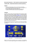
CHAPTER 2
SYSTEM DESCRIPTION
2. SYSTEM DESCRIPTION
In this chapter, a summary of the ST10x166 is presented.The following block diagram gives an overview of the different on-chip componentsand of the
advanced, high bandwidth internal bus structure of
the ST10F166.
Figure 2-1. Block Diagram
16
Internal
FLASH EPROM
32KBytes
ST10F166
32
Internal
RAM
1KBytes
16
CPU - CORE
16
PEC
...........
Interrupt Controller
OSC
XTAL
Wat chdog
16
16
GPT1
Ext.
16
Bus
Port 0
Control
10-bit USART USART
ADC
ASC0 ASC1
...
BRG
BRG
GPT2
CAPCOM
T2
T1
T3
T5
T4
T6
...
T0
2
Port 4
Port 1
16
Port 5
Port 3
10
16
Port 2
16
VR0 01613
1/6
2 - System Description
2.1 MEMORY ORGANIZATION
The memory space of the ST10x166 is configured
in a Von Neumann architecture which means that
code memory, data memory, registers and I/O
ports are organized within the same linear address
space which currently includes 256Kbytes. Address space expansion to 16 Mbytes is provided
for future versions. The entire memory space can
be accessed by byte or by word. Particular portions
of the on-chip memory have additionally been
made directly bit addressable.
The ST10166 contains 32Kbytes of mask-programmable on-chip ROM for code or constant
data.
The ST10F166 contains 32Kbytes of reprogrammable on-chip FLASH memory for code or constant data.
A large dual port RAM of 1Kbyte is contained on all
members of the ST10x166 family. This internal
RAM is provided as a storage for user defined variables, for the system stack, general purpose register banks and even for code. A register bank can
consist of up to 16 wordwide (R0 to R15) and/orbytewide (RL0, RH0, ..., RL7, RH7) called General
Purpose Registers (GPRs).
512 bytes of the address space are reserved for
the Special Function Register (SFR) area. SFRs
are wordwide registers which are used for controlling and monitoring functions of the different onchip units. 118 SFRs are currently implemented.
Unused SFR addresses are reserved for future
members of the ST10x166 family.
In order to meet the needs of designs where more
memory is required than is provided on chip, up to
256Kbytes of external RAM and/or ROM can be
connected to the microcontroller.
2.2 EXTERNAL BUS CONTROLLER
All of the external memoryaccesses are performed
by a particular on-chip External Bus Controller
(EBC). It can be programmed to either the Single
Chip Mode when no external memory is required,
or to one of four different external memory access
modes, which are as follows:
- 16-bit/18-bit Addresses, 16-bit Data, Non-Multiplexed
- 16-bit/18-bit Addresses, 16-bit Data, Multiplexed
- 16-bit/18-bit Addresses, 8-bit Data, Multiplexed
- 16-bit/18-bit Addresses, 8-bit data, Non-Multiplexed
2/6
In the non-multiplexed bus mode, Port 1 is used as
an output for addresses and Port 0 is used as an
input/output for data; the upper half of Port 0 can
not be used for general purpose I/O in the 8-bit
data bus mode. In the multiplexed bus modes, one
16-bit port, Port 0, is used as an input/output for
both addresses and data.
Important timing characteristics of the external bus
interface (Memory Cycle Time, Memory Tri-State
Time and Read/Write Delay) have been made programmable to allow the user the adaption of a wide
range of different types of memories. Access to
very slow memories is supported via a particular
‘Ready’ function.
For applications which require less than 64Kbytes
of memory space, a non-segmented memory
model can be selected. In this case, all memory locations can be addressedby 16 bits, and thus Port
4 is not needed as an output for the two most significant address bits (A17 and A16), as is the case
when using the segmented memory model.
2.3 CENTRAL PROCESSING UNIT (CPU)
The main core of the CPU consists of a 4-stage instruction pipeline, a 16-bit arithmetic and logic unit
(ALU) and dedicated SFRs. Additional hardware
has been spent for a separate multiply and divide
unit, a bit-mask generator and a barrel shifter.
Based on these hardware provisions, most of the
ST10x166’s instructions can be executed in just
one machine cycle which requires 100ns at 20MHz
CPU clock. For example, shift and rotate instructions are always processed during one machine
cycle independent of the number of bits to be
shifted. All multiple-cycle instructions have been
optimized so that they can be executed very fast as
well: A 32-bit/16-bit division in 1µs, a 16-bit x 16-bit
multiplication in 0.5µs, and branches in 200ns. Another pipeline optimization, the ‘Jump Cache’, allows reducing the execution time of repeatedly
performed jumps in a loop from 200ns to 100ns.
The CPU disposes of an actual register context
consisting of up to 16 wordwide GPRs which are
physically allocated within the on-chip RAM area.
A Context Pointer (CP) register determines the
base address of the active register bank to be accessed by the CPU at the time. The number of register banks is only restricted by the available
internal RAM space. For easy parameter passing,
register banks can also be organized to overlap.
2 - System Description
Figure 2-2. CPU Block Diagram
CPU
SP
MDH
R15
STKOV
32
1K
Bytes
RAM
MDL
STKUV
32K
Bytes
FLASH
EPROM
16
R15
Exec. Unit
Mul./Div.-HV
Instr. Ptr.
Bit-Mask Gen.
General
Purpose
Instr. Reg.
ALU
4 - Stage
Pipeline
Registers
(16-bit)
Barrel-Shifter
R0
PSW
SYSCON
Data Page P tr.
Context Ptr.
Code Seg. Ptr.
R0
16
VR 001 614
A system stack of up to 512 bytes is provided as a
storage for temporary data. The system stack is allocated in the on-chip RAM area, and it isaccessed
by the CPU via the stack pointer (SP) register. Two
separate SFRs, STKOV and STKUN, are implicitly
compared against the stack pointer value upon
each stack access for the detectionof a stack overflow or underflow.
The high performance offered by the hardware implementation of the CPU can efficiently be utilized
by a programmer via the highly functional
ST10x166 instruction set which includes the following instruction classes:
- Arithmetic Instructions
- Logical Instructions
- Boolean Bit Manipulation Instructions
-
Compare and Loop Control Instructions
Shift and Rotate Instructions
Prioritize Instruction
Data Movement Instructions
System Stack Instructions
Jump and Call Instructions
Return Instructions
System Control Instructions
Miscellaneous Instructions
The basic instruction length is either 2 or 4 bytes.
Possible operand types are bits, bytes and words.
A variety of direct, indirect or immediate addressing modes are provided to specify the required operands.
3/6
2 - System Description
2.4 INTERRUPT SYSTEM
With an interrupt response time within a range from
just 250ns to 500ns (in case of internal program
execution), the ST10x166 is capable of reacting
very quickly to the occurrence of non-deterministic
events.
The architecture of the ST10x166 supports several
mechanisms for fast and flexible response to service requests which can be generated from various
sources internal or external to the microcontroller.
Any of these interrupt requests can be programmed to be serviced by the Interrupt Controller
or by the Peripheral Event Controller (PEC).
In contrast to a standard interrupt service where
the current program execution is suspended and a
branch to the interrupt vector table is performed,
just one cycle is ‘stolen’ from the current CPU activity to perform a PEC service. A PEC service implies a single byte or word data transfer between
any two memory locations with an additional increment of either the PEC source or the destination
pointer. An individual PEC transfer counter is implicitly decremented for each PEC service except
when performing in the continuous transfer mode.
When this counter reaches zero, a standard interrupt is performed to the corresponding source related vector location. PEC services are very well
suited, for example, for supporting the transmission or reception of blocks of data, or for transferring A/D converted results to a memory table. The
ST10x166 has 8 PEC channels each of which offers such fast interrupt-driven data transfer capabilities.
A separate control register which contains an interrupt request flag, an interrupt enable flag and an interrupt priority bitfield, exists for each of the
possible interrupt sources. Via its related register,
each source can be programmed to one of sixteen
interrupt priority levels. Once having been accepted by the CPU, an interrupt service can only
be interrupted by a higher prioritized service request. For the standard interrupt processing, each
of the possible interrupt sources has a dedicated
vector location.
Software interrupts are supported by means of the
‘TRAP’ instruction in combinationwith an individual
trap (interrupt) number.
The ST10x166 also provides an excellent mechanism to identify and to process exceptions or error
conditions that arise during run-time, called ‘Hardware Traps’. Hardware traps cause immediate
non-maskable system reaction which is similiar to
a standard interrupt service (branching to a dedicated vector table location). The occurrence of a
hardware trap is additionally signified by a individual
4/6
bit in the trap flag register (TFR). Except another
higher prioritized trap service being in progress, a
hardware trap will interrupt any actual program
execution. In turn, hardware trap services can normally not be interrupted by standard or PEC interrupts.
2.5 CAPTURE/COMPARE (CAPCOM) UNIT
The CAPCOM unit supports generation and control of timing sequences on up to 16 channels with
a maximum resolution of 400ns. The CAPCOM
unit is typically used to handle high speed I/O tasks
such as pulse and waveform generation, pulse
width modulation (PWM), Digital to Analog (D/A)
conversion,software timing, or time recording relative to external events.
Two 16-bit timers (T0/T1) with reload registers provide two independent time bases for the capture/compare register array.
The input clock for the timers is programmable to
several prescaled values of the internal system
clock, or may be derived from an overflow/underflow of timer T6 in module GPT2.
This provides a wide range of variation for the timer
period and resolution and allows precise adjustment to the application specific requirements. In
addition, an external count input for CAPCOM
timer T0 allows event scheduling for the capture/compare registers relative to external events.
The capture/compare register array contains 16
dual purpose capture/compare registers, each of
which may be individually allocated to either CAPCOM timer T0 or T1, and programmed for capture
or compare function. Each register has one port
pin associated with it which serves as an input pin
for triggering the capture function, or as an output
pin to indicate the occurrence of a compare event.
When a capture/compare register has been selected for capturemode, the current contentsof the
allocated timer will be latched (‘captured’) into the
capture/compare register in response to an external event at the port pin which is associated with
this register. In addition,a specific interrupt request
for this capture/compare register is generated.
Either a positive, a negative,or both a positive and
a negative external signal transition at the pin can
be selected as the triggering event. The contents
of all registers which have been selected for one of
the five compare modes are continuously compared with the contents of the allocated timers.
When a match occurs between the timer value and
the value in a capture/compare register, specific
actions will be taken based on the selected compare mode.
2 - System Description
2.6 GENERAL PURPOSE TIMER (GPT) UNIT
The GPT unit represents a very flexible multifunctional timer/counterstructure which may be used for
many different time related tasks such as event timing and counting, pulse width and duty cycle measurement, pulse generation,or pulse multiplication.
The GPT unit incorporates five 16-bit timers which
are organized in two separate modules, GPT1 and
GPT2.Eachtimer in each module may operateindependentlyin a number of different modes, or may be
concatenated with another timer of the same module.
Each of the three timers T2, T3, T4 of the GPT1
module can be configured individually for one of
three basic modes of operation, which are Timer,
GatedTimer, andCounterMode.In Timer Mode, the
inputclock for a timer is derivedfrom theinternalsystem clock, divided by a programmable prescaler,
while Counter Mode allows a timer to be clocked in
reference to external events.
Pulse width or dutycycle measurement is supported
in Gated Timer Mode,where the operationof a timer
is controlled by the ‘gate’ level on an external input
pin. For these purposes, each timer has one associated port pin which servesas gateor clock input.The
maximum resolution of the timers in the GPT1 module is 400ns (@fOSC=40MHz).
The count direction (up/down) for each timer is programmable by software. For timer T3, the count direction may additionallybe altereddynamically by an
external signal on a port pin to facilitate e.g. position
tracking.
Timer T3 has an output toggle latch which changes
its state on each timer overflow/underflow.Thestate
of this latch may be output on a port pin e.g for time
out monitoring of externalhardware components,or
may be used internally to clock timers T2 and T4 for
measuring long time periods with high resolution.
In addition to their basic operatingmodes, timers T2
and T4 may be configured as reload or capture registers for timer T3. When used as capture or reload
registers, timers T2 and T4 are stopped. The contents of timer T3 are captured into T2 or T4 in response to a signal at their associated input pins.
Timer T3 is reloaded with the contents of T2 or T4
either by an external signal or by a selectable state
transition of its toggle latch. When both T2 and T4
are configured to alternately reload T3 with the low
and high times of a PWM signal, this signal can be
constantlygeneratedwithout software intervention.
With its maximum resolution of 200ns
(@fOSC=40MHz), the GPT2 module provides precise event control and time measurement. It in-
cludes two timers (T5, T6) and a capture/reload
register (CAPREL). Both timers can independently
count up or down, clocked with an input clock
which is derived from a programmable prescaler.
Concatenation of the timers is supported via the
output toggle latch of timer T6, which changes its
state on each timer overflow/underflow.
The state of this latch may be used to clock timer
T5, or it may be output on a port pin. Overflows/underflows of timer T6 can additionally be used to
clock the CAPCOM timers T0 or T1, and to cause
a reload from the CAPREL register. The CAPREL
register may capture the contents of timer T5
based on an externalsignal transition on the corresponding port pin, and timer T5 will be cleared by
this external transition if the clear function is enabled. This allows absolute time differences to be
measured or pulse multiplication to be performed
without software overhead.
2.7 A/D CONVERTER
For analog signal measurement, a 10-bit A/D converterwith 10 multiplexed inputchannelsand a sample and hold circuit has been integrated on-chip. It
uses the methodof successive approximation which
returns the conversion result for an analog channel
within 9.75µs @ fOSC=40MHz.
Overrun error detection capability is provided for the
conversionresult register:an interrupt requestwill be
generatedwhen the result of a previous conversion
has not been read from the result register at the time
the next conversionis complete.
For applications which require less than 10 analog
input channels, the remaining channels can be used
as digital input port pins.
The A/D converter of the ST10x166 supports four
different conversion modes. In the standard Single
Channel conversion mode, the analog level on a
specified channel is once sampled and converted
into a digital result. In the Single Channel Continous
mode, the analog level is repeatedly sampled and
convertedwithout softwareintervention.
In the Auto Scan mode, the analog levels on a prespecified number of channelsare sequentiallysampled and converted. In the Auto Scan Continuous
mode, the number of prespecified channels is repeatedlysampled and converted.
The Peripheral Event Controller (PEC) may be used
to automatically store the conversion results into a
table in memory for later evaluation, without requiring the overhead of entering and exiting interrupt
routines for each data transfer.
5/6
2 - System Description
2.8 SERIAL CHANNELS
Serial communication with other microcontrollers,
processors, terminals, or external peripheral components is provided by two serial interfaces with
identical functionality, Serial Channel 0 (ASC0)
and Serial Channel 1 (ASC1).
Both channels support full-duplex asynchronous
communication up to 625Kbaud and half-duplex
synchronous communication up to 2.5 Mbaud.
Two dedicated baud rate generators allow to set
up all standard baud rates without oscillator tuning.
For transmission, reception, and erroneous reception 3 separate interrupt vectors are provided for
each serial channel.
In the synchronous mode, one data byte is transmitted or received synchronously to a shift clock
which is generated by the ST10x166. In the asynchronous mode, an 8- or 9bit data frame is transmitted or received, preceded by a start bit and
terminated by one or two stop bits. For multiprocessor communication, a mechanism to distinguish
address from data bytes has been included (8-bit
data+wake up bit mode), and a loop back option is
available for testing purposes.
A number of optional hardware error detection capabilitieshas been included to increase the reliability of data transfers. A parity bit can automatically
be generatedon transmission or be checked on reception. Framing error detection allows the recognition of data frames with missing stop bits. An
overrun error will be generatedif the last character
received has not been read out of the receive buffer register at the time reception of a new character
is complete.
2.9 WATCHDOG TIMER
The Watchdog Timer of the ST10x166 represents
one of the fail-safe mechanisms which have been
implemented to prevent the controller from malfunctioning for longer periods of time.
The Watchdog Timer of the ST10x166 is always
enabled after a reset of the chip, and can only be
disabled in the time interval until the EINIT (end of
initialization) instruction has been executed. Thus,
the chip’s start-up procedure is always monitored.
6/6
When the software has been designed to service
the Watchdog Timer before it overflows, the
Watchdog Timer times out if the program does not
progress properly due to hardware or software related failures. When the Watchdog Timer overflows, it generates an internal hardware reset and
pulls the RSTOUT pin low in order to allow external
hardware components to reset.
The Watchdog Timer of the ST10x166 is a 16-bit
timer which can either be clocked with fOSC/4 or
fOSC/256. The high byte of the Watchdog Timer
register can be set to a prespecifiedreload value in
order to allow further variation of the monitored
time interval. Each time it is serviced by the application software, the high byte of the Watchdog
Timer is reloaded. Thus, time intervals between
25µs and 420ms can be monitored (@fOSC=40MHz).
The default Watchdog Timer interval after reset is
6.55ms.
2.10 PARALLEL PORTS
The ST10x166 provides 76 I/O lines which are organized into four 16-bit I/O ports (Port0 through 3),
one 2-bit I/O port (Port 4), and one 10-bit input port
(Port 5). All port lines are bit addressable, and all
lines of Port 0 through 4 are individually bit-wise
programmable as inputs or outputs via direction
registers. The I/O ports are true bidirectional ports
which are switched to the high impedance state
when configured as inputs. During the internal reset, all port pins are configured as inputs.
Each port line has one programmable alternate input or output function associated with it. Ports 0
and 1 may be usedas addressand data lines when
accessing external memory, while Port 4 outputs
the additional segment address bits A16 and A17
in systems where segmentation is enabled to access more than 64Kbytes of memory. Port 2 is associated with the capture inputs/compare outputs
of the CAPCOM unit, and Port 3 includes alternate
functions of timers, serial interfaces, optional bus
control signals (WR,BHE,READY), and the system
clock output (CLKOUT). Port 5 is used for the analog input channelsto the A/D converter. When anyone of these alternate functions is not used, the
respective port line may be used as general purpose I/O line.
CHAPTER 3
MEMORY ORGANIZATION
3. MEMORY ORGANIZATION
The ST10x166 family’s memory space is configured in a von Neumann architecture. This means
that code and data are accessed within the same
linear address space. All of the physically separated memory areas, including the internal ROM
(for the ST10166, internal FLASH memory for the
ST10F166), internal RAM, internal Special Function Registers (SFRs), and external memory are
mapped into a common address space.
The ST10x166 provides a total addressable memory space of 256Kbytes.
This address space is arranged in four segments
of 64Kbyteseach, and each segment is again subdivided in four pages of 16Kbytes each. The total
addressable memory space can be expanded up
to 16 Mbytes for future members of the ST10x166
family.
Figure 3-1. Memory Segment And Page Arrangement
Data
Page
Address
3FFFFh
Code
Segment
15
14
3
13
30000h
12
2FFFFh
11
10
2
9
20000h
8
1FFFFh
7
6
1
5
10000h
4
0FFFFh
3
2
0
1
00000h
0
256KByte
Total Address
Space
1/10
3 - Memory Organization
Bytes are stored at even or odd byte addresses.
Words are stored in ascending memory locations
with the low byte at an even byte address being followed by the high byte at the next odd byte address. Double words (code only) are stored in
ascending memory locations as two subsequently
following words. Single bits are always stored in
the specified bit position at a word address. Bit position 0 is the least significant bit of the byte at an
even byte address, and bit position 15 is the most
significant bit of the byte at the next odd byte address.
Figure 3-2. Word, Byte And Bit Storage In a Byte Organised Memory (Example)
. . .
xxxx6h
15
14
. . . Bits . . .
8
xxxx5h
7
6
. . . Bits . . .
0
xxxx4h
Byte
xxxx3h
Byte
xxxx2h
Word (High Byte)
xxxx1h
Word (Low Byte)
xxxx0h
. . .
xxxxFh
Table 3.1 shows how the different memory areas
are mapped into the physical 256Kbyte address
space. Basically, all of the internal memory areas
(ROM or FLASH memory, RAM, SFRs) are
mapped into parts of memory segment 0. The external memory is mapped into the remaining parts
2/10
of memory segment 0 and into memory segments
1 through 3. Whenever the Program memory has
been disabled during reset, or remapped to segment 1 during initialisation, the lowest 32Kbytes of
segment 0 also specify an external memory area.
3 - Memory Organization
Table 3-1. Memory Address Space Mapping
Address Space
Memory Range
Size (Bytes)
00000h - 07FFFh
Internal Program Memory Segment 0
or External Memory
32K
08000h - 0F9FFh
External Memory
30.5K
0FA00h - 0FDFFh
Internal Memory (RAM)
1K
0FE00h - 0FFFFh
Internal SFRs
512
10000h - 17FFFh
Internal Program Memory Segment 1
or External Memory
32K
18000h - 3FFFFh
External Memory
160K
The internal program memory, the internal RAM
and the external memory space can be used for
general code and data storage. The internal SFR
space is provided for control data, but not for code
storage.
Note that byte units forming a singleword or a double word must always be stored within the same
physical and organizational memory area (page,
segment).
A particular use is provided for some memory areas, as follows. Addressesfrom 00000h to 000BFh
in code segment zero are reserved for the hardware trap and interrupt vector jump table. The active General Purpose Register Bank which is
selected by the Context Pointer (CP) Register can
be situated anywhere in the internal RAM area (addresses from 0FA00h to 0FDFFh). Word addresses from 0FA00h to 0FBFEh in the internal
RAM can basically be used for the system stack
implementation. The highest 32 bytes of the internal RAM (addresses from 0FDE0h to 0FDFFh) are
provided for the Peripheral Event Controller (PEC)
source and destination pointers. Three memory
spaces (from 0FF00h to 0FFDFh in the internal
SFR area, from 0FD00h to 0FDFFh in the internal
RAM area, and the address space occupied by the
currently selected register bank) are basically provided for single bit accesses.
Figure 3.3 gives an overview of the memory organization of the ST10x166. For more details
about the different memory areas see the corresponding subsections in this chapter. The principles of the physical address generation are
described in section 6.2 (Addressing Modes).
Chapter 9 is dedicatedto the External Bus Controller which is responsible for all of the memory accesses made externally.
3/10
4/10
Stack
Pointer
Context
Pointer
0FA00h
0FBFFh
0FD00h
0FE00h
0FDFFhh
0FDE0h
INTERNAL MEMORY
1KByte
Internal RAM
System Stack
GPRs
PEC Source and
Destination Pointers
512Bytes
Internal SFRs
0FF00h
0FFFFh
0FFE0h
0FFDFh
Bit Addressable
Space
00000h
07FFFh
Internal
Memory
30000h
Code Segment 1
Code Segment 3
32KBytes 17FFFh
External
Memory
20000h
or
Code Segment 2
Internal
FLASH
Memory 10000h
64KBytes
External
Memory
1FFFFh
VR001615
INTERNAL/EXTERNAL MEMORY
Code Segment 0
External
Memory
32KBytes
Internal
FLASH
Memory
or
30.5KBytes
External
Memory
0FFFFh
32KBytes
External
Memory
64KBytes
External
Memory
2FFFFh
3FFFFh
3 - Memory Organization
Figure 3-3. Memory Organization
3 - Memory Organization
3.1 INTERNAL PROGRAM MEMORY
3.2 EXTERNAL MEMORY
The Program memory is an on-chip mask-programmable ROM for the ST10166, and on-chip reprogrammable FLASH memory for the ST10F166.
The memory is organized in 8Kx32bits and
mapped in the same segment memory: segment 0
during reset or segment 1 if remapped during initialization. This program memory is enabled during reset with the pin BUSACT high and the
external bus configuration pins EBC1 and EBC0
low. This mode is named the Single Chip Mode.
For further details about the external bus configuration see chapter 9.
The internal Program memory can be used for both
code and data storage. The highest possible code
storage location in this memory is 07FFEh for 16bit instructions or 07FFCh for 32-bit instructions. A
branch instruction is neededto cross the boundary
between the internal Program memory to the external memory, otherwise this would cause erroneous results.
No short addressing mode and bit addressable
mode are allowed for any accesses to the internal
Program memory. For PEC data transfers, these
accesses are independent of the contents of the
DPP registers via the PEC source and destination
pointers.
Whenever a reset, hardware trap or interrupt occurs, or whenever a software TRAP instruction is
executed, and provided that the Program memory
accesses are enabled, program execution
branches to an implicit internal address independent of the current Code Segment Pointer
(CSP) register contents, expecting a jump vector
being situated there. For detailed information
about the trap and interrupt jump vector table see
section 9.1 ”Interrupt System Structure”.
With the possibility to remap the internal Program
memory to segment 1 during initialization, however,the user can configure the device with common routines and constants programmed into the
Program memory to have a fast execution speed
and with the interrupt vector programmed into External memory.
For the ST10F166, the special features of the
FLASH memory are described in the FLASH memory chapter 4.
Basically, the ST10x166 provides for up to 4 x
64Kbytesof external ROM and/or RAM which may
be organized in either 8 or 16 bits. Since a part of
the first 64Kbytes address space is already occupied by the on-chip memory areas, only 62.5Kbytes (30.5Kbytes for the ST10F166 and ST10166
with internal program memory enabled) of external
memory are really available in segment 0.
The bus mode for external memory accessesis selected during reset by means of the external bus
configuration pins, BUSACT, EBC1 and EBC0.
According to there logic levels, external memory
accesses are either enabled or disabled during reset, as shown in chapter 9. The selected external
bus configuration is saved in the BTYP bit field in
the SYSCON register. During the initialization routine, however, the user has the option to change
any configuration which was selected during reset.
After the EINIT instruction, only the external bus
configurationcan be changed at any time.
For further details about the external bus configuration and control see chapter 9 ”External Bus Interface”.
The external memory can be used for both code
and data storage. If the ST10x166 segmentation
mode is disabled (SGTDIS bit in the SYSCON register contains a ‘1’), all external memory accesses
are restricted to segment 0 only. Code accesses
are always made on even byte addresses. Thus,
the highest possible external code storage location
in segment 0 is either 0F9FEh for single word instructions or 0F9FCh for double word instructions.
If used for code storage, the corresponding location must contain a branch instruction, because sequential boundary crossing from the external
memory to the internal RAM space is not provided
and would cause erroneous results. In any segment other than 0, the highest code storage location is either xFFFEh for single word instructions or
xFFFCh for double word instructions (x=1, 2, 3). If
used for code storage, the corresponding location
must contain a branch instruction, because segment crossing for program execution is only possible by changing the CSP register contents by
means of the particular branch instructions JMPS
and CALLS.
5/10
3 - Memory Organization
External word and byte data can only be accessed
via indirect or long 16-bit addressing modes in collaborationwith the DPP registers. Thereis no short
addressing mode for external operands. Any word
data access is made to an even byte address.
Thus, the highest possible word data storage locations in the external memory are address 0F9FEh
in segment 0, and addresses xFFFEh in all other
segments (x=1, 2, 3). For PEC data transfers, the
externalmemory in segment 0 can be accessedindependentof the contents of the DPP registers via
the PEC source and destination pointers.
The external memory is not provided for single bit
storage, and thus it is not bit addressable.
Whenever a reset, a hardware trap or an interrupt
occurs, or whenever a software TRAP instruction
is executed, and provided that internal program
memory accesses are disabled, program execution branches to an implicit external memory address independent of the current CSP register
contents, expecting a jump vector being situated
there. For detailed information about the trap and
interrupt jump vector table see section 7.1 ‘Interrupt System Structure’.
3.3 INTERNAL RAM
The ST10x166 contains 1Kbyte of on-chip dual
port RAM which is organized in 512x16 bytes. Internal RAM accesses are always enabled.
The system stack, the General Purpose Registers
(GPRs) and the PEC source and destination pointers are situatedwithin the internal RAM space. Additionally, the internal RAM can be used for both
code and data storage. The ST10x166 assembler
supports the reservation of the required internal
RAM areas according to the just mentioned particular uses.
Code accesses are always made on even byte addresses. Provided that the PEC source and destination pointers are not required, the highest
possible code storage location in the internal RAM
6/10
is either 0FDFEh for single word instructions or
0FDFCh for double word instructions. If used for
code storage, the corresponding location must
contain a branch instruction to a memory location
other than in the SFR space, because this space is
not provided for code execution.
Any word and byte data in the internal RAM can be
accessed via indirect or long 16 bit addressing
modes if the selected DPP register points to data
page 3. Any word data access is made on an even
byte address. Provided that the PEC source and
destination pointers are not required, the highest
possible word data storage location in the internal
RAM is address 0FDFEh. For PEC data transfers,
the internal RAM can be accessed independent of
the contents of the DPP registers via the PEC
source and destination pointers.
All system stack operations are implicitly performed by means of the Stack Pointer (SP) register. The GPRs are accessed via short 2-, 4- or 8-bit
addressingmodes in collaborationwith a particular
Context Pointer (CP) register. The channel number of a PEC data transfer to be performed determines which PEC source or destination pointers
will be implicitly accessed. All of the just mentioned
implicit internal RAM accesses are made independent of the current DPP register contents.
The upper portion of the internal RAM (addresses
from 0FD00h to 0FDFFh) and the currently active
GPRs are provided for single bit storage, and thus
they are bit addressable.
The following subsections describe in more detail
the organization of the system stack, of the GPRs
and of the PEC source and destination pointers.
3.3.1 System Stack
The internal RAM address space from 0FBFFh
downward to 0FA00h is basically provided for the
ST10x166’s system stack implementation. The default maximum stack size of 256 words can easily
be reduced by changing the stack size (STKSZ) bit
field in the SYSCON register, as shown in the following table.
3 - Memory Organization
Table 3-2. Maximum System Stack Size Selection
STKSZ
Stack Size (words)
Internal RAM Addresses (in descending order)
00b
256
0FBFFh - 0FA00h
01b
128
0FBFFh - OFB00h
10b
64
0FBFFh - OFB80h
11b
32
0FBFFh - 0FBC0h
For all system stack operations, the on-chip RAM
is accessed via the Stack Pointer (SP) register.
The stack grows downward from higher towards
lower RAM address locations. Only word accesses
are permitted to the system stack. A stack overflow
(STKOV) and a stack underflow (STKUN) register
are provided to control when the selected stack
area is left. These two stack boundary registers
can be used not only for protection against data
destruction, but also to implement a circular stack
with hardware supported system stack flushing
and filling.
For further details about system stack addressing
via the SP register and the use of the STKOV and
STKUN registers see section 5.3 ‘CPU Special
Function Registers’.
(default)
3.3.2 General Purpose Registers
The ST10x166’s GPRs can basically be situated
anywhere within the internal RAM address space
(addresses from 0FA00h to 0FDFFh). A particular
Context Pointer (CP) register determines the base
address of the currently active register bank. This
register bank may consist of up to 16 word GPRs
(R0, R1, ..., R15) and/or of up to 16 byte GPRs
(RL0, RH0, ..., RL7, RH7). The sixteen byte GPRs
are mapped onto the first eight word GPRs, as
shown in figure 3.4.
In contrast to the system stack, a register bank
grows from lower towards higher address locations
and occupies a maximum space of 32bytes. Short
4- and 8-bit addressing modesin collaborationwith
the CP register support word or byte GPR ac-
7/10
3 - Memory Organization
Figure 3-4. Word and Byte GPR Organization
WORD Register R15
WORD Register R14
WORD Register R13
WORD Register R12
WORD Register R11
WORD Register R10
WORD Register R9
WORD
WORD Register R8
Register
BYTE Register RH7
BYTE Register RL7
R7
BYTE Register RH6
BYTE Register RL6
R6
BYTE Register RH5
BYTE Register RL5
R5
BYTE Register RH4
BYTE Register RL4
R4
BYTE Register RH3
BYTE Register RL3
R3
BYTE Register RH2
BYTE Register RL2
R2
BYTE Register RH1
BYTE Register RL1
R1
BYTE Register RH0
BYTE Register RL0
R0
cesses regardless of the current DPP register contents. Additionally, each bit in the currently active
register bank can be accessed individually.
The ST10x166 supports fast register bank (context) switching. Based on that, multiple register
banks can physically exist in the internal RAM at
the same time. However, only the register bank selected by the CP register is active, and the remaining register banks are inactive at that time.
Selecting a new active register bank is simply done
by updating the CP register. A particular Switch
Context (SCXT) instruction performs register bank
8/10
←
CP
switching and an automatic saving of the previous
context. Any number of variously sized register
banks, only limited by the available internal RAM
size, can be implemented simultaneously.
For more details about GPR addressing via the CP
register, see the chapter 5. Advanced programming methods for an optimum utilization of the
GPRs’ features such as Context Switching, Context Packing, Overlapping Register Banks, Local
GPRs on the system stack and so on, are described in chapter 13 ‘System Programming’.
3 - Memory Organization
3.3.3 Pec Source and Destination Pointers
The upper 16 word locations in the internal RAM
(addresses from 0FDE0h to 0FDFEh) are provided
as source and destination address pointers for
PEC data transfers.
As shown in figure below, a pair of source and destination pointers is stored in two subsequently following word memory locations with the source
pointer (SRCPx) on the lower and with the destination pointer (DSTPx) on the higher word address
(x=0 to 7).
Whenever a PEC data transfer is performed, the
pair of source and destination pointers which is selected by the specified PEC channel number is accessed independent of the current DPP register
contents. If a PEC channel is not used, the corresponding pointer locations can be used for word,
byte or single bit data storage.
For more details about the use of the source and
destination pointers for PEC data transfers refer to
chapter 7.
Figure 3-5. PEC Source And Destination Pointer Word Organization
FDFEh
DSTP7
FDFCh
SRCP7
SFRs
FE00h
FDFEh
FDE0h
FDDEh
PEC
Source
and
Destination
Pointers
FDE2h
DSTP0
FDE0h
SRCP0
Internal
RAM
FA00h
External
Memory
F9FEh
9/10
3 - Memory Organization
3.4 INTERNAL SPECIAL FUNCTION
REGISTERS
The ST10x166 provides 512bytes of on-chip Special Function Register (SFR) space. The SFRs are
mapped into the address space from 0FE00h to
0FFFFh.
The SFRs are not provided for general code or
data storage, but for data storagededicated to very
particular uses, mainly for controlling CPU, Peripheral and I/O functions.
According to the just mentioned control functions,
the SFRs are described in detail in one of the chapters 5 ‘CPU’, 8 ‘Peripherals’, or 10 ‘Parallel Ports’.
A table containing a short description, symbolic addresses, physical 18-bit and short 8-bit addresses
of the SFRs can be found in appendixB.
Most commonly, an SFR can be accessedby word
via an implicit base address plus a short8-bit offset
address independent of the current DPP register
contents. The low byte portion of an SFR (but not
its high byte portion!) can be accessed via these
short 8 bit addressing modes. However, provided
10/10
that the selected DPP register points to data page
3, any high byte, low byte or any word in the SFR
memory space can be accessed via an indirect or
long 16-bit addressing mode.
The upper portion of the SFR memory space (addresses from 0FF00h to 0FFDFh) contains SFRs
with many single flag control functions. Thus, this
memory area is directly bit addressable.
Some bits in already existing SFRs and some word
locations in the SFR address space have been reserved for a future implementationof additionalonchip peripherals. Any intended write access to
such a reserved SFR memory space would be ignored by the machine, and any intended read will
supply a read result of ‘0’.
Note that any byte write to an existing SFR causes
the non-addressed complementary byte to be
cleared.
Some SFRs or parts of them have a restricted access type such as read-onlyor write only. For more
details, see the functional description of the corresponding SFRs.
CHAPTER 4
ON-CHIP FLASH MEMORY
4. ON-CHIP FLASH MEMORY
The ST10F166 provides, in addition to the on-chip
RAM, 32K bytes of Electrically Erasable and Reprogrammablenon-volatile (FLASH) memory. This
memory is organised as 8Kx32 bits, allowing a
complete instruction to be read during one instruction fetch cycle. Data values stored can be read as
16 bit operands using all addressing modes of the
ST10x166 instruction set.
The FLASH memory is located in segment 0 (0 to
07FFFh) during reset, and thus contains the
power-on reset and interrupt vectors. To provide
full flexibility in the use of the ST10F166, the
FLASH memory may be remapped to segment 1
(10000 to 17FFFh) during initialization. This allows
the interrupt vectors to be programmed from external memory, while retaining the common routines
and constants programmed into the FLASH memory.
For erase or program updating, the FLASH memory is organised into 4 banks (12K, 12K, 6K and
2K) each of which may be independentlyerased.
Optionally the FLASH Memory may be protected
against read and write accesses performed by
fetch instructions from programs running in the internal RAM or in external memory.
All control of programming and erasing the FLASH
memory is made from one Register, the FLASH
Control Register (FCR), which is virtually mapped
into the FLASH memory space.
The Presto F algorithm is used for reliability. The
typical programming time is 100µs and erase time
is 1s. The FLASH memory features a typical endurance of 100 erase/write cycles.
WARNING: Access to or code execution from the
FLASH memory can not be performed during an
erase or programming operation on the FLASH
memory. Therefore the appropriate routines must
be executed from internal RAM or external memory outside of the FLASH memory address range.
Figure 4-1. Flash Memory Architecture
HIGH VOLTAGE
MANAGEMENT
32Bits
BIDIRECTIONAL
INTERFACE
+
FLASH
TIMER
+
PROTECTION
ADDRESS
DECODER
+
READ/WRITE
CIRCUIT
MATRIX
1/8
4 - Flash Memory
FLASH MODES
This section describes the differents modes used
with the FLASH memory and is detailed in the following sections.
Normal mode:
This mode is the standard mode of the FLASH
memory. In this operation mode, the FLASH memory works exactly as the 32K bytes ROM of the
ST10166 with the same timing and functionality.
Therefore only instruction fetches or data operand
reads are performed in this mode with all the addressing modes of the ST10x166 instruction set.
No read or write operations on the FCR register
are possible in this mode, except the protection bit
(RPROT) which can be modified in this mode but
only from a program instruction within the FLASH
memory.
Figure 4-2. Flash Modes Description
2/8
Write mode:
As it is not possible to fetch instructions from and
write to the FLASH memory at the same time, a
Write mode has been defined. In this mode FLASH
memory accesses can be made only with indirect
addressing modes and FCR register is accessed
with direct access modes.
In Write mode, all programming and erase operations on the FLASH memory are controlledby software with the Flash Control Register (FCR).
Thereforeto write the FLASH memory, the FWE bit
of FCR register has to be set to ”1”.
To enter the Write Program mode, the FEE bit of
FCR register has to be cleared. If FEE and FWE of
FCR register are set to ”1”, the Erase mode is entered.
In these two modes, a Verify mode is automatically
entered when the programming or erase operation
is ended, respectivly Program Verify Mode (PVM)
and Erase Verify Mode (EVM).
4 - Flash Memory
FLASH CONTROL REGISTER
During the normal operation mode, the FLASH
memory is read as normal ROM memory with all
addressingmodes of the ST10x166.
All programming(1) or erase operations of the
FLASH memory are controlled via the Flash Control Register (FCR).
To prevent inadvertent writing of the FLASH memory, FCR is locked and inactive during the normal
operationmodes. The FLASH memory must be set
into the Write mode to provide a valid access to the
FCR. A key code sequence is used to enter the
Write mode.
The FCR is virtually located within the address
space of the FLASH memory (it does not occupy
an absolute address) and is only accessed with a
direct addressing mode.
When the segmented memory mode is enabled,
the data page pointer must be considered for all
FCR accesses.
Note 1: Accordingto the IEEE Standardon floating
gate arrays, the following terminology is used: writing means a state change of the floating gate, programming means the loading of electrons onto the
floating gate, erase means the removal of electrons from the floating gate.
FCR
Flash Control Register
Reset Condition: 0000h
15
14
13
11
10
R
FWMSET
7
12
6
5
4
3
2
FBUSY
WDWW CKCTL1 CKCTL0 VPPRIV FCVPP RPROT
9
8
BE1
BE0
1
0
FEE
FWE
b15 = FWMSET: will be set at a logical ”1”, once
the Write mode has been entered. This bit must be
set to ”1” at each writing of the FCR for an erase or
programming operation. It will stay set at ”1” when
the operation has ended. The user must reset
FWMSET to exit from the FLASH memory Write
mode. At ”0” during reset.
b14 to b10 = R : reserved for future development,
must be written to ”0”.
b8,9 = BE0,1 : select the different Banks for Erase
as shown in the following Table:
In state ”0” during reset.
BE1
BE0
Bank
Addresses (segment0)
0
0
1
1
0
1
0
1
0
1
2
3
00000h to 02FFFh
03000h to 05FFFh
06000h to 077FFh
07800h to 07FFFh
b7= WDWW : if set at a logical ”1”, enables a 32 bit
operation, otherwise it will be a 16 bit operation. At
”0” during reset.
b5,6 = CKCTL0,1 : select the FLASH internal timer
as shown in Table below:
In state ”0” during reset.
CKCTL1
CKCTL0
0
0
1
1
0
1
0
1
TPRG
1/TCL = 2 to 40MHz
2
4.10
4.103
4.104
4.105
TCL
TCL
TCL
TCL
The maximum programming pulse (PT) allowed is
200µs with a maximum programming time of
2.5ms. Therefore the value ’00b’ covers all the frequency range.
The maximum erasing pulse (ET) allowed is 10ms
with a maximum erasing time of 30s.
At 20MHz CPU clock, ’11b’ is the recommended
value. At 1MHz CPU clock, ’01b’ is the recommended value.For all other frequencies, ’10b’ is
recommended
b4 = VPPRIV: READ ONLY bit reflects the status
of VPP in the write mode. If VPP is not high enough
for reliable programming, it will be at a logical ”0”.
The reset value depends on thestatus of the external Vpp on the EBC1/Vpp pin.
b3 = FCVPP: READ ONLY bit, if set at a logical”1”,
will indicate to the user that VPP voltage has gone
below the programming threshold during a programming or erase operation. At ”0” during reset.
b2 = FBUSY: READ ONLY bit is set at a logical ”1”
during a program/erase operation. At ”0” during reset.
b2 = RPROT: WRITE ONLY bit is used when the
protected FLASH option is chosen. This bit, set at
a logical ”1” and with the option selected, will enable protection. At ”1” during reset.
b1= FEE : if set at a logical ”1”, will enable the
erase operation; otherwise ”0” for the programming operation. At ”0” during reset.
b0= FWE: if set at a logical ”1”, will enable the writing operation; the programming or erase operation
is selected depending on the state of FEE bit; otherwise ”0” for reading mode. At ”0” during reset.
3/8
4 - Flash Memory
FLASH MEMORY PROTECTION
A programmable option, set by the FLASH Programming Board, prevents any access to the
FLASH memory from the internal RAM or External
memory.
When this option is enabled, the configuration of
the FLASH memory depends on the RPROT bit of
FCR.
Protection Option
Enabled
RPROT
bit
Protection
Active
Yes
Yes
No
No
1
0
1
0
Yes
No
No
No
This bit is set at ”1” during reset, so any access to
the FLASH memory from the internal RAM or External memory is disabled and access to FCR is allowed only from the FLASH memory.
To disable the protection, the following instruction
has to be performed in the normal mode and from
the FLASH memory ONLY:
MOV
MEM,Rn
where MEM is any even absolute address in the
FLASH memory space. The RPROT bit of FCR (bit
2 of Rn) must be reset, the other bits of FCR are
protected in the normal mode and are not affected.
When the protection is disabled, reading of the
FLASH memory can be performed from all internal or external memory. Access to FCR register and the FLASH programming or erase
operations is available only after having entered the Write mode.
THE WRITE MODE
To enter the Write mode a key code sequence of
two dummy write instructions has to be performed:
MOV
MEM,Rn
MOV
[Rn],Rn
where MEM is any even absolute address in the
FLASH memory space and Rn a General Purpose
Register loaded with the even address of any value
within the FLASH memory address space (segment 0 or segment 1).
The FWMSET bit of FCR is automatically set by
the unlock sequence.
Once in Write mode, all read and write accesses to
FCR are enabled. However, before performing the
FIRST programming or erase operation, a delay of
10µs must be executed. The device requires this
time to set up the internal high voltage.
When the FLASH memory is mapped in segment
0, it is recommendedto disable the interrupts when
in write mode, as they would not be served if the
program code is the FLASH memory.
When the FLASH memory is mapped in segment 1, some care must be taken for the management of interrupts during the write mode.
The unlock sequence and the 32-bit programming sequence must not be interrupted.
All erase or programming operations and verify sequencescan be interrupted,if no FLASHreading is
performedfrom an external program (internal RAM
or external memory) during the interrupt.
To exit from the Write mode to the normal mode,
the following instruction has to be performed:
MOV
MEM,Rn
where bit 15 of Rn must be ”0” to disable the Write
mode (FWMSET) and MEM is any even absolute
address in the FLASH memory space.
Note: When the segmented memory mode is enabled, the data page pointer must be considered
for all FLASH memory accesses.
4/8
4 - Flash Memory
FLASH PROGRAMMING OPERATION
Afterthe Write mode has been entered, the FLASH
memory is accessed for programming with indirect
addressing mode instructions. One or two words
(word = 16 bits) can be programmed at once, depending on the WDWW bit value of FCR.
A programming operation is realized with the following sequence:
- Test VPPRIV bit of FCR to verify the correct
voltage on VPP.
- Load the desired value in FCR.
15
14
13
1
0
0
7
6
5
FWMSET
12
11
10
0
0
0
4
3
2
R
WDWW CKCTL1 CKCTL0 VPPRIV FCVPP FBUSY
0/1
0/1
0/1
0
0
0
9
8
BE1
BE0
0
0
1
0
FEE
FWE
0
1
As FCR is a virtual register, all bits previously written must be confirmed in the same state at each
FCR writing (especially FWMSET).
- Write the FLASH memory
e.g. for one word
MOV
[Rm],R1
for two words
MOV
[Rm],R1
MOV
[Rm],R2
The address used for a long word write (32 bits)
Rm must be an aligned even address (xxx0h,
xxx4h, xxx8h, xxxCh...) and is used as a base
pointer for the FLASH memory writing. The two
words to write must be contiguous, aligned at an
even address.
R1 contains the data to write at the first address
and R2 contains the data to write at the following
even word address.
-
FLASH programming will automatically start.
The programming time depends on CKCTL0,1
bits of FCR. End of programming is detected
by polling on the FBUSY bit of FCR.
Test FCVPP bit of FCR to verify that VPP had
- the
correct voltage during programming.
After
programming, the FWE bit remains at a
logical ”1”. The Program Verify Mode (PVM), is
then entered automatically. An internally generated margin voltage is applied to the FLASH,
and reading valid data indicates the word has
been programmed successfully.
PVM needs a double read instruction with the
same operand and time to stabilize the internal circuitry.
e.g.
MOV
R1,[R2]
;
Time out of 4µs
MOV
R1,[R2]
-
To perform normal reading of the FLASH memory, the FWE bit must be reset.
A programming operation of the FLASH memory
can not be performed with a routine in the FLASH
memory itself.
FLASH ERASE OPERATION
As for the programming operation, FLASH memory erase can be performed only inside the Write
mode, with indirect addressing mode instruction.
One of the four Banks is erased performingthis operation, dependingon the BE0,1 bits of FCR.
An erase operation is realized with the following
sequence:
Program all the words of the relevant bank
- to
0000h.
Test
VPPRIV bit of FCR to verify the correct
voltage on VPP.
- Load the desired value in FCR.
5/8
4 - Flash Memory
15
14
13
1
0
0
7
6
5
FWMSET
12
11
10
0
0
0
4
3
2
R
WDWW CKCTL1 CKCTL0 VPPRIV FCVPP FBUSY
0
0/1
0/1
0
0
0
9
8
BE1
BE0
0/1
0/1
1
0
FEE
FWE
1
1
As FCR is a virtual register, all bits previously written must be confirmed in the same state at each
FCR writing (especially FWMSET).
- Perform the erase command
e.g. MOV [R0],R0
This special instruction for erase, guarantees users against inadvertent operation.
erase will automatically start. The
- FLASH
erase time depends on CKCTL0,1 bits of FCR.
End of erase is detected by polling on the
FBUSY bit of FCR.
- Test FCVPP bit of FCR to verify that VPP had
the correct voltage during erase.
all the FLASH memory must be read to
- Then
verify the completely correct erasure. After erasure, bits FWE and FEE remain at a logical ”1”.
The Erase Verify Mode (EVM), is then entered
automatically.
An internally generated margin voltage is applied to the FLASH memory. If the memory location is erased, the Erase Verify is repeated
for the next location. This process continues for
each word of the array until the last address is
accessed or a word does not return FFFFh. In
this case where the word is not erased, another erase operation must be performed.
EVM needs a double reading instruction with the
same operand, and time for stabilizing the internal
circuitry.
e.g.
MOV R1,[R2]
Time out of 4ms
MOV R1,[R2]
-
To perform a normal FLASH reading, the
FWE,FEE bits must be reset.
The erase of one bank can not be performed from
another bank of the FLASH memory.
6/8
PRESTO F PROGRAM WRITE ALGORITHM
Programming with Presto F algorithm consists of
applying a sequence of program pulses to each
word until correct verify occurs. A maximum of
programming operations are allowed for each
word. Each program operation consists of a program command; the programming is then automatically performed. After a time out of 4µs a Program
Verify is then performed which compares data output with data expected. This sequence guarantees
that each cell is programmed reliably.
Figure 4.3 illustrates the Presto F Program Write
Algorithm.
As the program pulse varies in inverse ratio to the
frequency,PT=400 TCL, the number of operations
allwed varies also:
N=6250/TCL with I/TCL= 2 to 40MHz.
PRESTO F ERASE ALGORITHM
Erasing with Presto F algorithm allows the electrically erasing of the selected Bank in a reliable way.
The algorithm starts by first programming all the
words to 0000h in order to perform an uniform erasure. This step is performed by using the Presto F
Program Write Algorithm.
The erase command (see erase operation) is written and erase is performed. An Erase Verify begins
at the first address and continues until the last address is accessedor until the comparison of data to
FFFFh fails. The address of the last word verified is
stored and a new erase operation is performed.
Then the Erase Verify restarts from the stored address.
Figure 4.4 illustrates the Presto F Erase Algorithm.
As the erasing pulse (ET) varies in inverse ratio to
the frequency, the number of erasing operation
varies also:
at 1MHz CPU clock ET = 2ms, N = 15000
at 40 MHz CPU clock ET = 10ms, N = 3000
4
for other frequenciesET = 4.10 TCL,
4
N = 75.10 /TCL
4 - Flash Memory
Figure 4-3. Presto F Program Write Algorithm
7/8
4 - Flash Memory
Figure 4-4. Presto F Erase Algorithm
8/8
CHAPTER 5
CENTRAL PROCESSING UNIT (CPU)
5. CENTRAL PROCESSING UNIT
Basic tasks of the CPU are to fetch and decode instructions, to supply operands for the arithmetic
and logic unit (ALU), to perform operations on
these operands in the ALU, and to store the previously calculated results. Since a four stage pipeline is implemented in the ST10x166, up to four
instructions can be processed in parallel. Section
5.1 describes how the pipelineworks for sequential
and branch instructions in general, and which
hardware provisions have been made to speed the
execution of jump instructions in particular.
With reference to instruction pipelining, most
ST10x166 instructions can be regarded as being
executed during one machine cycle (=100ns at
40MHz oscillator frequency). Section 5.2 describes the general instruction timing including
standard and exceptional timing.
While internal memory accesses are normally performed by the CPU itself, all of the external memory accesses are performed by a particular on-chip
External Bus Controller (EBC) which is automatically invoked by the CPU whenever a code or data
address belongs to the external memory space. If
possible, the CPU continues operatingwhile an external memory access is in progress. If external
data are required but are not yet available, or if a
new external memory access is requested by the
CPU before a previous access has been completed, the CPU will be held by the EBC until the request can be satisfied. Chapter 9 is dedicated to a
description of the external bus interface being
serviced by the EBC.
The ST10x166 peripherals work nearly independent of the CPU with a separate clock generator. An interchange of data and control
information between the CPU and the peripherals
is done via Special Function Registers (SFRs).
Whenever peripherals non-deterministically need
a CPU action, an on-chip Interrupt Controller compares all pending peripheral service requests
against each other and prioritizes one of them. If
the priority of the current CPU operation is less
than the priority of the selected peripheral request,
an interrupt will occur.
Basically, there are two types of interrupt processing: One type, the standard interrupt processing,
forces the CPU to save the current program status
and the return address on the stack before branching to the interrupt vector jump table. The second
type, the PEC interrupt processing, steals just one
machine cycle from the current CPU activity to perform a single data transfer via the on-chip Peripheral Event Controller (PEC). System errors
detected during program execution (so called
hardware traps), or an external non-maskable interrupt are also processed as standard interrupts
with a very high priority. For more information
about interrupts, PEC data transfers and hardware
traps see chapter 7.
In contrast to other on-chip peripherals, there is a
closer conjunction between the Watchdog Timer
and the CPU. If enabled, the Watchdog Timer expects to be serviced by the CPU within a programmable period of time, otherwise it will reset the
chip. Thus, the Watchdog Timer is able to prevent
the CPU from going totally astray when executing
erroneous code. After reset, the Watchdog Timer
starts countingautomatically,but it canbe disabled
via software if desired.
By any reset, the CPU is forced into a predefined
active state. Further particular CPU states are: The
IDLE state where the CPU clock is switched off and
the peripheral clocks keep running, and the
POWER DOWN state where all of the on-chip
clocks are switched off. A transition into an active
CPU state is forced by an interrupt if being IDLE, or
by a reset if being in POWER DOWN mode, respectively. The IDLE, POWERDOWN and RESET
states can be entered by particular ST10x166 system control instructions. For more information on
these states see chapter 12.
1/26
5 - Central Processing Unit
Section5.3 describes the Special Function Registers situated within the CPU core which are all
dedicated to particular uses, as follows:
General System Configuration: SYSCON
Bus Configuration: BUSCON1
Address Select: ADDRSEL1
CPU Status Indication and Control: PSW
Code Access Control: IP, CSP
Data Paging Control: DPP0, DPP1, DPP2,
DPP3
GPRs Access Control: CP
SystemStackAccess Control:SP,STKUN, STKOV
Multiply and Divide Support: MDL, MDH, MDC
ALU Constant Support: ZEROS, ONES
struction. All explicit writes to the SFR memory
space and all auto-increment or auto-decrement
writes to GPRs used as indirect address pointers
are performed during the execute stage of an instruction, too.
4th -> WRITE BACK: In this stage, all external operands and the remaining operands within the internal RAM space are written back.
A particularity of the ST10x166 are the so called injected instructions. These injected instructions are
internally generated by the machine to provide the
time needed to process instructions which cannot
be processed within one machine cycle.They are
automatically injected into the decode stage of the
pipeline, and then they pass through the remaining
stages as every standard instruction. Program interrupts are performed by means of injected instructions, too. Although one will not notice these
internally injected instructionsin reality, they are introduced here to ease the explanationof the pipeline in the following.
5.1 INSTRUCTION PIPELINING
As mentioned in the introductional part of this
chapter, a four stage instruction pipeline is implemented in the ST10x166. This means that instruction processing is partitioned in four stages of
which each one has its individual task as follows:
1st -> FETCH: In this stage, the instruction selected by the Instruction Pointer and the Code Segment Pointer is fetched from either the internal
ROM or FLASH memory, internal RAM, or external
memory.
2nd -> DECODE: In this stage, the instructions are
decoded, and if required,the operand addresses
are calculated and the resulting operands are
fetched. For all instructions which implicitly access
the system stack, the SP register is either decremented or incrementedas specified. For branch instructions, the Instruction Pointer and the Code
Segment Pointer are updated with the desired
branch target addresses (provided that the branch
is taken).
3rd -> EXECUTE: In this stage, an operation is
performed on the previously fetched operands in
the ALU. Additionally, the condition flags in the
PSW register are updated as specified by an in-
5.1.1 Sequential Instruction Processing
Each single instruction has to pass through each of
the four pipeline stages regardless of whether all
possible stage operations are really performed or
not. Since passing through one pipeline stage
takes at least one machine cycle, any single instruction takes at least four machine cycles to be
completed. Pipelining, however, allows parallel
(this means simultaneous) processing of up to four
instructions. Thus, most of the instructions seem to
be processed during one machine cycle as soon
as the pipeline has been filled once after reset (see
figure 5.1).
Instruction pipelining increases the average instruction throughput considered over a certain period of time. In the following, any execution time
specification of an instruction always refers to the
average execution time due to pipelinedparallel instruction processing.
Figure 5-1. Sequential Instruction Pipelining
→
FETCH
DECODE
1 Machine
Cycle
I1
←
time
→
I2
I3
I4
I5
I6
I1
I2
I3
I4
I5
I1
I2
I3
I4
I1
I2
I3
EXECUTE
WRITE BACK
2/26
5 - Central Processing Unit
5.1.2 Standard Branch Instruction Processing
Instruction pipelining helps to speed sequential
program processing. In the case that a branch is
taken, the instruction which has already been
fetched providently is mostly not the instruction
which must be decoded next. Thus, at least one
additional machine cycle is normally required to
fetch the branch target instruction. This extra machine cycle is provided by means of an injected in-
struction as shown in figure 5.2.
If a conditionalbranch is not taken, there is no deviation from the sequential program flow, and thus
no extra time is required. In this case, the instruction after the branch instruction will enter the decode stage of the pipeline at the beginning of the
next machine cycle after decode of the conditional
branch instruction.
Figure 5-2. Standard Branch Instruction Processing
→
FETCH
1 Machine
Cycle
←
injection
time
→
BRANCH
In + 2
ITARGET
ITARGET + 1
ITARGET + 2
ITARGET + 3
DECODE
In
BRANCH
(IINJECT)
ITARGET
ITARGET + 1
ITARGET + 2
EXECUTE
...
In
BRANCH
(IINJECT)
ITARGET
ITARGET + 1
WRITE BACK
...
...
In
BRANCH
(IINJECT)
ITARGET
5.1.3 Cache Jump Instruction Processing
A jump cache has been incorporated in the
ST10x166 as an optimization of conditional jumps
which are processed repeatedly within a loop.
Whenever a jump on cache is taken, the extratime
to fetch the branch target instruction can be saved,
and thus the correspondingcache jump instruction
in most cases takes only one machine cycle to be
performed.
This performance is achieved by the following
mechanism. Whenever a cache jump instruction
passes through the decode stage of the pipeline
for the first time (and provided that the jump condition is met), the jump target instruction is fetched
as usual causing a time delay of one machine cycle. In contrast to standard branch instructions,
however, the target instruction of a cache jump in-
struction (JMPA, JMPR, JB, JBC, JNB,JNBS)is additionally stored in a cache after having been
fetched.
After each repeatedly following execution of the
same cache jump instruction, the jump target instruction is not fetched but taken from the cache
and immediatly injected into the decode stage of
the pipeline (see figure 5.3).
A time saving jump on cache is always taken after
the second and any further occurence of the same
cache jump instruction, unless an instruction which
has the fundamental capability of changing the
CSP register contents (JMPS, CALLS, RETS,
TRAP, RETI) or any standard interrupt has been
processed during the period of time between two
following occurences of the same cache jump instruction.
Figure 5-3. Cache Jump Instruction Pipelining
→
FETCH
Injection of Cached
Target Instruction
Injection
1 Machine
Cycle
←
In + 2
ITARGET
ITARGET + 1
In+2
ITARGET + 1
ITARGET + 2
DECODE
Cache Jump
(IINJECT)
ITARGET
Cache Jump
ITARGET
ITARGET + 1
EXECUTE
In
Cache Jump
(IINJECT)
In
Cache Jump
ITARGET
...
In
Cache Jump
. ..
In
Cache Jump
WRITE BACK
1st loop iteration
→
Repeated loop iteration
→
3/26
5 - Central Processing Unit
5.1.4 Particular Pipeline Effects
Since up to four different instructions are processed
simultaneously,additionalhardware has been spent
inthe ST10x166to considerall causal dependencies
which may exist on instructions in different pipeline
stages without a loss of performance. This extra
hardware (i.e. for ‘forwarding’ operand read and
write values) avoids that the pipeline becomes noticeablefor the user in most of the cases.
However, there are somevery rare cases whereone
must pay attention to the circumstance that the
ST10x166 is a pipelined machine. Intelligent
ST10x166 tools like the simulator and the emulator
support the user by easing the association with the
following particular pipelineeffects.
Context Pointer Updating
An instructionwhich calculatesa physicalGPRoperand address via the CP register is mostly not capable of using a new CP value which is to be updated
by an immediatelyprecedinginstruction.Thus, if one
surely wants the new CP value to be used,one must
put at least one instruction between a CP-changing
and a subsequentGPR-using instruction, as shown
in the following example:
SCXT CP, #0FC00h
In
; select a new context
In+1
....
; must not be an instruction using a GPR
R0, #dataX
In+2 MOV
; write to GPR 0 in the new context
Data Page PointerUpdating
An instruction which calculates a physical operand
address via a particular DPPn (n = 0 to 3) register is
mostly not capable of using a new DPPn register
value which is to be updated by an immediately preceding instruction. Thus, if one surely wants the new
DPPn register value to be used, one must put at
least one instruction between a DPPn-changing instruction and a subsequentinstruction which implicitly uses DPPn via a long or indirect addressing
mode, as shown in the following example:
In
MOV
DPP0, #4
; select data page 4 via DPP0
....
In+1
; must not be an instruction using DPP0
; (for long or indirect addresses from 0000h
; to 3FFFh)
In+2 MOV
0000h, R1
; move contents of GPR 1 to address
; location 10000h (in data page 4)
; supposed that segmentation is not
; disabled
4/26
Explicit Stack Pointer Updating
Any of the RET, RETI, RETS, RETP or POP instructions is not capable of correctly using a new SP register value which is to be updatedby an immediately
precedinginstruction. Thus, if onewants the new SP
register value to be used without erroneously performed stack accesses,one must put at leastone instruction between an explicitly SP-writing and any
subsequentof the just mentionedimplicitly SP-using
instructions,as shown in the following example:
In
MOV
SP, #0FA40h
; select a new top of stack
In+1
....
; must not be an instruction popping
; operands from the system stack
In+2 POP R0
; pop the word value from the new top of
; stack into GPR 0
External Memory Access Sequences
The effect described here will only become noticeable if one looks at the externalmemory access sequences on the external bus (i.e. by means of a
Logic Analyzer). Different pipeline stages can simultaneously put a request on the External Bus
Controller (EBC). Since the predefined priority of
external memory accesses is as follows, 1st Write
Data, 2nd Fetch Code, 3rd Read Data, the sequence of instructions processed by the CPU may
diverge from the sequence of the corresponding
external memory accesses performed by the EBC
.
Timing
As already described, instruction pipelining reduces the average instruction processing time in a
wide scale (from four to one machine cycles). However, there are some rare cases where a particular
pipeline situation causes a single instruction processing time to be extended either by a half or by
one machine cycle. Although this additional time
represents only a tiny part of the total program execution time, it might be of interest to avoid these
pipeline-caused time delays in time critical program modules.
Besides a general execution time description, section 5.2 provides some hints how one can optimize
time-critical program parts with regard to such
pipeline-caused timing particularities.
5 - Central Processing Unit
5.2 INSTRUCTION STATE TIMES
Basically, the time to execute an instruction depends on where the instruction is fetched from, and
where possible operands are read from or written
to. The fastest processingmode of the ST10x166 is
to execute a program fetched from the internal program memory. In that case, most of the instructions
can be processed within just one machine cycle,
which also represents the general minimum execution time.
All of the external memory accesses are performed
by the ST10x166 on-chip External Bus Controller
(EBC) which works in parallel with the CPU. Mostly,
instructions from the external memory can not be
processed as fast as instructions from the internal
program memory, because some data transfers
which internally can be performed in parallel, have
to be performed sequentially via the external interface. In contrast to internal program memory program execution, the time required to process an
external program additionally depends on the
length of the instructions and operands, on the selected bus mode, and on the durationof an external
memory cycle which is partly selectableby the user.
Processinga program from the internal RAM space
is not as fast as execution from the internal ROM
area, but it offersa lot of flexibility (i.e., for end of line
programming where a program could be loaded into
the internal RAM via the chip’s serial interface).
The following description allows evaluating the
minimum and maximum program execution times.
This will be sufficient for most of the requirements.
This section is arranged in subsectionsof which the
first one defines the subsequently used time units,
the second contains an overview about the minimum (standard) state times of the ST10x166 instructions, and the third describes the exceptions
from that standard timing.
5.2.1 Time Unit Definitions
The following time units are used to describe the
instruction processing times:
[fOSC]: Oscillator frequency (may be variable
from 2MHz to 40MHz).
[State]:One state time is specified by two times
an oscillator period. Henceforth, one
State is used as the basic time unit, because it represents the shortest period of
time which has to be considered for instruction timing evaluations.
1 [State] = 2 x 1/fOSC [s]; for fOSC = variable
= 50 [ns] ; for f OSC = 40MHz
[ACT]: This ALE (Address Latch Enable) Cycle
Time specifies the time required to perform one external memory access. One
ALE Cycle Time consists of either two
(for a non-multiplexed external bus
mode) or three (for a multiplexed external
bus mode) state times plus a number of
state times which is determined by the
number of wait states programmed in the
MCTC (Memory Cycle Time Control) and
MTTC (Memory Tristate Time Control) bit
fields of the SYSCON register plus one
state time if ALECTL1 bit of ADDRSEL1
register is set to ‘1’.
In the case of the non-multiplexed external bus mode:
1xACT =(2+(15 - MCTC)+(1- MTTC)
+(ALECTL1))xStates
= 100ns ... 900ns ; for f OSC = 40MHz
In the case of the multiplexed external
bus modes:
1x ACT=3 + (15 -MCTC) + (1 - MTTC
+(ALECTL1)) x States
= 150ns ... 950ns ; for f OSC = 40MHz
The total time (Ttot) which a particular part of a program takes to be processed can be calculated by
the sum of the single instruction processing times
(TIn) of the considered instructions plus an offset
value of 6 state times which considers the solitary
filling of the pipeline, as follows:
Ttot = TI1 + TI2 + ... + TIn + 6 x States
The time T In which a single instruction takes to be
processed consists of a minimum number (TImin)
plus an additional number (TIadd) of instruction
state times and/or ALE Cycle Times, as follows:
TIn = TImin + TIadd
5.2.2 Minimum State Times
The following table 5.1 shows the minimum number of state times required to process a ST10x166
instruction fetched from the internal ROM (TImin
(ROM)). The minimum number of state times for instructions fetched from the internal RAM (TImin
(RAM)), or of ALE Cycle Times for instructions
fetched from the external memory (TImin (ext)), can
also be easily calculated by means of table 5.1.
Most of the ST10x166 instructions - except some
of the branches, the multiplication, the division and
a special move instruction - require a minimum of
two state times. In the case of internal ROM pro-
5/26
5 - Central Processing Unit
gram execution there is no execution time dependency on the instructionlength except for some special branch situations. The injected target
instruction of a cache jump instruction can be considered for timing evaluations as if being executed
from the internal ROM, regardless of which memory range the rest of the current program is really
fetched from.
For some of the branch instructions, table 5.1 represents both the standard number of state times
which means that the corresponding branch is
taken, and an additional TImin value in parentheses
which refers to the case that either the branch condition is not met or that a cache jump is taken.
Instructions executed from the internal RAM require the same minimum time as if being fetched
from the internal ROM plus an instruction-length
dependentnumber of state times, as follows:
For 2-byte instructions:
TImin(RAM) =TImin (ROM) + 4 x States
For 4-byte instructions:
TImin(RAM) =TImin (ROM) + 6 x States
In contrast to the internal ROM program execution,
the minimum time TImin(ext) to process an external
instruction additionally depends on the instruction
length. TImin(ext) is either 1 ALE Cycle Time for
most of the 2-byte instructions, or 2 ALE Cycle
Times for most of the 4-byte instructions. The following formula represents the minimum execution
time of instructions fetched from an external memory via a 16-bit data bus:
For 2-byte instructions:
TImin(ext)=1xACT + (TImin(ROM) - 2) x States
For 4-byte instructions:
TImin(ext)=2xACTs + (TImin(ROM) - 2) x States
For instructions fetched from an external memory
via an 8-bit data bus, the minimum number of required ALE Cycle Times is twice the number for a
16-bit bus.
Table 5-1. Minimum Instruction State Times
TImin (ROM)
[States]
Instruction
TImin (ROM)
(at 20MHz CPU Clock)
2
Any (except the following)
Unit
100
ns
4
4
4
4
4
10
20
4
4
4
CALLI, CALLA
CALLS, CALLR, PCALL
JB, JBC, JNB, JNBS
JMPS
JMPA, JMPI, JMPR
MUL, MULU
DIV, DIVL, DIVU, DIVLU
MOV[B] Rn, [Rm + #data 16]
RET, RETI, RETP, RETS
TRAP
5.2.3 Additional State Times
As described in the following, some operand accesses can extend the execution time of an instruction, TIn. Since the additional time, TIadd, is
mostly caused by internal instruction pipelining, it
often will be possible to evade these timing effects
in time-critical program modules by means of a
suitable rearrangement of the corresponding instruction sequences.The ST10x166 simulator and
emulator offer many facilities which support the
user in optimizing the program whenever required.
6/26
(2)
(2)
(2)
200
200
200
200
200
500
1000
200
200
200
(100)
(100)
(100)
ns
ns
ns
ns
ns
ns
ns
ns
ns
ns
1 )Internal ROM operand reads: TIadd = 2x States
Both byte and word operand reads always require
2 additional state times.
2) Internal RAM operand reads via indirect addressing modes: TIadd = 0 or 1 x State
Reading a GPR or any other directly addressed
operand within the internal RAM space does NOT
cause additional state times. However, reading an
indirectly addressed internal RAM operand will extend the processing time by 1 state time if the pre-
5 - Central Processing Unit
ceding instruction auto-increments or auto-decrements a GPR as shown in the following example:
MOV R1 , [R0+]
In
; auto-increment R0
In+1 MOV [R3], [R2]
; if R2 points into the internal RAM space:
; T Iadd = 1 x State
In this case, the additional time can simply be
avoided by putting another suitable instruction before the instruction In+1 indirectly reading the internal RAM.
3)Internal SFR operand reads:
TIadd = 0, 1 x State or 2 x States
Mostly, SFR read accesses do NOT require additional processing time. In some rare cases, however, either one or two additionalstate times will be
caused by particular SFR operations,as follows:
- Reading an SFR immediately after an instruction which writes to the internal SFR space, as
shown in the following example:
In
MOV
T0, #1000h
; write to Timer 0
In+1 ADD
R3, T1
; read from Timer 1: TIadd = 1 x State
the PSW register immediately after an
- Reading
instruction which implicitly updates the condition flags, as shown in the following example:
In
ADD
R0, #1000h
; implicit modification of PSW flags
In+1 BAND
C, Z
; read from PSW: TIadd = 2 x States
incrementing or decrementing the SP
- Implicitly
register immediately after an instruction which
explicitly writes to the SP register, as shown in
the following example:
MOV SP, #0FB00h
In
; explicit update of the stack pointer
In+1 SCXT R1, #1000h
; implicit decrement of the stack pointer:
; T Iadd = 2 x States
In these cases, the extra state times can be
avoided by putting other suitable instructions before the instruction In+1 reading the SFR.
4) External operand reads: TIadd = 1 x ACT
Any external operand reading via a 16-bit data bus
requires one additional ALE Cycle Time. Reading
word operands via an 8-bit data bus takes twice as
much time (2 ALE Cycle Times) as the reading of
byte operands.
5) External operand writes:
TIadd = 0 x State ... 1 x ACT
Writing of an external operand via a 16-bit data bus
takes one additional ALE Cycle Time. For timing
calculations of external program parts, this extra
time must always be considered. The value of TIadd
which must be considered for timing evaluations of
internal program parts, may fluctuate between 0
state times and 1 ALE Cycle Time. This is because
external writes are normally performed in parallel
to other CPU operations. Thus, TIadd could already
have been considered in the standard processing
time of another instruction. Writing a word operand
via an 8-bit data bus requires twice as much time
(2 ALE Cycle Times) as the writing of a byte operand.
6)Testing Branch Conditions:
TIadd = 0 or 1 x States
Mostly, NO extra time is required for conditional
branch instructions to decide whether a branch
condition is met or not. However, an additional
state time will be caused if the preceding instruction writes to the PSW register, as shown in the following example:
In
BSET USR0
; write to PSW
In+1 JMPR cc_Z, label
; test condition flag in PSW:
; TIadd = 1 x State
In this case, the extra state time can simply be intercepted by putting another suitable instruction
before the conditional branch instruction.
7) Jumps into the internal ROM space:
TIadd = 0 or 2 x States
As already described, standard jumps into the internal ROM space require 4 state times to be executed. This minimum time will be extended by 2
additional state times, if the branch target instruction is a double word instruction at a non-aligned
double word location (xxx2h, xxx6h, xxxAh,
xxxEh), as shown in the following example:
label ....
; any non-aligned double word instruction
; (i.e. at location 0FFEh)
....
....
In+1 JMPA cc_UC, label
; if a standardbranch is taken:
; TIadd = 2 x States (TIn = 6 x States)
A cache jump, which normally requires just 2 state
times, will be extended by 2 additional state times
if both the cached jump target instruction and its
7/26
5 - Central Processing Unit
successor instruction are non-aligned double word
instructions, as shown in the following example:
label ....
; any non-aligned double word instruction
; (i.e. at location 12FAh)
It+1
....
; any non-aligned double word instruction
; (i.e. at location 12FEh)
In+1 JMPR cc_UC, label
; provided that a cache jump is taken:
; T Iadd = 2 x States (TIn = 4 x States)
If required, these extra state times can be avoided
by allocating double word jump target instructions
to aligned double word addresses (xxx0h, xxx4h,
xxx8h, xxxCh).
5.3 CPU SPECIAL FUNCTION REGISTERS
The core CPU requires a set of Special Function
Registers (SFRs) to maintain the system state information,to supply the ALU with register-addressable constantsand to control system configuration,
multiply and divide ALU operations, code memory
segmentation,data memory paging, and accesses
onto the General Purpose Registers and the System Stack.
The access mechanism for these SFRs in the CPU
core is identical to the access mechanism for any
other SFR. Since all SFRs can simply be controlled
by means of any instruction which is capable of addressing the SFR memory space, a lot of flexibility
has been gained, and the need to create a set of
system specific instructions was avoided. Note,
however, that there are user access restrictions for
some of the CPU core SFRs to ensure proper processor operations.
The PSW, SP, and MDC registers can be modified
not only explicitly by the programmer, but also implicitly by the CPU during normal instruction processing. Note that any explicit programmer’s write
request to an SFR supersedes a simultaneous
modification by hardware of the same register.
Note furthermore, that any byte write operation to
an SFR clears the non-addressed complementary
byte within the specified SFR. Note also that nonimplemented (reserved) SFR bits can not be modified, and will always supply a read value of ‘0’.
8/26
SYSCON (FF0Ch / 86h)
System Configuration Register
Reset Values: 0000h, 0400h, 0440h, 0480h or
04C0h
15
14
R
13
STKSZ
7
6
BTYP
12
11
10
9
8
RDYEN SGTDIS BUSACT BYTDIS CLKEN
5
4
MTTC
RWDC
3
2
1
0
MCTC
b15 = R: Reserved.
b14,b13 = STKSZ: Maximum System Stack Size
Selection of between 32 and 256 words.
b12 = RDYEN: READY Input Enable control bit:
RDYEN = 0: READY disabled; pin can be used
for normal I/O
RDYEN = 1: READY enabled; pin used for
READY input
b11 = SGTDIS: SegmentationDisable controle bit:
SGTDIS = 0: A16 and A17 enabled; Port 4 used
for segment address
SGTDIS = 1: A16 and A17 disabled; Port 4 can
be used for normal I/O
b10 = BUSACT: Bus Active Control Bit.
b9 = BYTDIS: Byte High Enable (BHE) pin control
bit:
BYTDIS = 0: BHE enabled
BYTDIS = 1: BHE disabled; pin can be used for
normal I/O
b8 = CLKEN: System Clock Output (CLKOUT) Enable bit :
CLKEN = 0: CLKOUT disabled; pin can be used
for normal I/O
CLKEN = 1: CLKOUT enabled; pin used for system clock output
b7,b6 = BTYP: External Bus Configuration Control
b5 = MTTC: Memory Tri-state Time Control
b4 = RWDC: Read/Write Delay Control.
b3,b2,b1,b0= MCTC: Memory Cycle TIme Control.
5 - Central Processing Unit
5.3.1 SYSCON: System Configuration
Register
This bit-addressable register provides general system configuration and control functions. There are
five different reset values for the SYSCONregister,
becausethe BTYP bit field and the BUSACT bit are
initialized during reset dependent on the state of
the BUSACT, EBC0 and EBC1 input pins.
5.3.1.1 INTERNAL ROM OR FLASH MEMORY/EXTERNAL MEMORY ACCESS MODE SELECTION
A two-bit field, BTYP, and BUSACT, reflect the selected external bus configuration, as shown in table 5.2.
BTYP bits and the BUSACT bit are always readand writeable bits, regardless of the bus configuration selected during reset. But after the EINIT
instruction (end of initialization), only the external
bus configuration can be changed at any time.
When the SYSCON parameters are modified during initialization, an instruction from a source (external bus or internal ROM) which is to be switched
must not be performed.(e.g. disabling the external
bus when executing from external memory)!
Switching between the bus modes can also be performed with the BUSCON1 register. (see section
5.3.1.5 for further information).
Note that the selection of a multiplexed external
bus configuration automatically extends the Memory Tri-State Time by one state time (1 state
time=2 x 1/fOSC).
For further information and for examples about the
Single Chip Mode and the external bus configuration modes, see section 9.1.
5.3.1.2 EXTERNAL BUS TIMING CONTROL (VIA
MCTC, MTTC, RWDC)
The MCTC bit field and the MTTC and RWDC bits
in the SYSCON register are provided for varying
external bus timing parameters as follows. The
Memory Cycle Time can be extended within a
range from 0 to 15 state times by means of the
MCTC bit field (1 state time = 2 x 1/fOSC). By means
of the MTTC bit, the Memory Tri-State time can be
extendedby either 1 or 0 additionalstate time. The
Memory Tri-State Time is additionallyextended by
one state time whenever a multiplexed external
bus configurationis selected. The RWDC bit allows
programming a time delay of either 0 or 0.5 state
times between the falling edges of the ALE and the
Read/Write signals. This read/write delay does not
extend the general memory access time. Note that
additionalexternal wait states do not slow down internal memory accesses. Table 5.3 summarizes
the SYSCON control functions for the external bus
timing.
Afterreset, the MCTC, MTTC and RWDC are all initialized to zero. Thus, even very slow memories
will be accessed correctly.
5.3.1.3 BYTE HIGH ENABLE PIN CONTROL (VIA BYTDIS)
The BYTDIS bit is provided for controlling the active low Byte High Enable (BHE) pin. The function
of the BHE pin is enabled if the BYTDIS bit contains a ‘0’. Otherwise, it is disabled and the pin can
be used as standardI/O pin. The BHE pin is implicitly used by the External Bus Controller to select
one of two byte-organizedmemorychips which are
connected with the ST10x166 via a word wide-external data bus. After reset, BYTDIS is initialized to
zero.
For further information about the use of the BHE
pin see chapter 10.
Table 5-2. External Bus Configuration via BUSACT, BTYP bit field
BUSACT
BTYP
Reset
During Init
After Init
0
0
0
0
00
01
10
11
ROM enable Seg. 0 No ext. Bus
(Reserved)
(Reserved)
(Reserved)
ROM enable Seg. 0
ROM enable Seg. 1
Disable ROM
Disable ext. Bus
No Action
No Action
No Action
No Action
1
1
1
1
00
01
10
11
8-Bit Non-Mux no ROM
8-Bit Mux no ROM
16-Bit Mux no ROM
16-Bit Non-Mux no ROM
8-Bit Non-Mux
8-Bit Mux
16-Bit Mux
16-Bit Non-Mux
8-Bit Non-Mux
8-Bit Mux
16-Bit Mux
16-Bit Non-Mux
9/26
5 - Central Processing Unit
Table 5-3. SYSCON External Bus Timing Control Functions
Control
Parameter
Value
Number of Additional
State Times
Affected Time
MCTC
0000b
0001b
0010b
0011b
0100b
0101b
0110b
0111b
1000b
1001b
1010b
1011b
1100b
1101b
1110b
1111b
15
14
13
12
11
10
9
8
7
6
5
4
3
2
1
0
MTTC
0b
1b
1
0
Memory Tri-State Time
RWDC
0b
1b
0
0
Read/Write Signal Delay
00b
01b
10b
11b
0
1
1
0
BTYP
5.3.1.4 READY PIN CONTROL (VIA RDYEN)
The RDYEN bit provides an optional Data-Ready
function via the active low READY input pin, to allow an external memory controller or peripherals to
determine the duration of an external memory access. The Data-Ready function is enabled by setting the RDYEN bit to ‘1’. In this case, port pin
P3.14 takes on its alternate function as active low
READY input pin. An active low signal on the
READY input pin signifies that data is available
and must be latched by the on-chip External Bus
Controller. Note, that it is the user’s responsibility
to set the direction of the READY pin to input before using this function.
When the Data-Ready function is enabled and bits
0 to 2 of SYSCONregister are cleared, the external
bus timing is only determined by the READY pin,
the MTTC bit, the RWDC bit and by the selected
external bus mode. If 1 to 7 wait states are programmed in bits 0 to 2 of the MCTC field, the CPU
will first insert the selected number of wait states
10/26
Memory Cycle Time
(implicit)
(implicit)
Memory Tri-State Time
(implicit for multiplexed
bus configurations)
into the memory cycle (Cycle Time Wait States),
regardless of the state of the READY line. Then after the wait state time has expired, the CPU will
check the READY line and delay the memory access dependingon the state of the READY line.
Warning: If the Data-Ready function is enabled,
the READY input pin must be activated for every
external memory access. Otherwise, the system
would be halted until a reset occurs. No time-out
protectionother than a WatchdogTimer overflow is
provided for that case.
In order to allow one to interface to a variety of peripherals, support for both asynchronous and synchronous modes of operation is provided. If the
Data-Ready function is enabled, bit 3 in the SYSCON register (the MSB of the MCTC bit field) determines whether the READY input pin is to be
used in asynchronousor synchronous mode:
SYSCON.3 = 1:Asynchronous READY input
SYSCON.3 = 0:Synchronous READY input
5 - Central Processing Unit
In the asynchronous mode of operation, the
READY input signal is internally synchronized to
the microcontroller’s operation. In this case, an additional delay of up to two state times may be required in order to internally synchronize the signal.
In the synchronous mode of operation, it is the
user’s responsibility to ensure that the READY input signal meets the specified setup and hold
times. In order to obtain the necessary timing information and to perform external synchronization,
the Clock Output function can be used.
After reset, the Data-Ready function is disabled.
5.3.1.5 CLOCK OUTPUT PIN CONTROL (VIA CLKEN)
The Clock Output function is enabled by settingthe
CLKEN bit of the SYSCON register to ‘1’. If enabled, port pin P3.15 takes on its alternate function
as CLKOUT output pin. The Clock Output is a 50%
duty cycle clock whose frequency is half the oscillator frequency (fOUT = fOSC/2). For a 40MHz clock
oscillator, the CLKOUT frequency is 20MHz.
Note that it is the user’s responsibility to set the direction of the CLKOUT pin to output and to write a
‘1’ into port latch P3.15 before using this function.
After reset, the Clock Output function is disabled.
5.3.1.6 NON-SEGMENTED MEMORY MODE SELECTION (VIA SGTDIS)
The SGTDIS bit allows selecting either the segmented or non-segmented memory mode. In the
caseof the non-segmentedmemorymode (SGTDIS
= ‘1’), the entire address space is restricted to 64
Kbytes (segment 0), and thus all addresses can be
represented by 16-bits. Thus, the contents of the
CSP register are totally ignored, and only the two
leastsignificant bits of the DPP registers are usedfor
physical address generation. This means also that
the pins of Port 4 can be used as standard I/O pins.
In the case of the segmented memory mode
(SGTDIS = ‘0’), the CSP and DPP registersare used
for the generation of physical 18-bit addresses as
described in sections 5.3.6 and 5.3.7. The pins of
Port 4 are used as address pins A17 and A16 provided that an external bus has been configured.
Whenever the segmented memory mode is selected, the CSP register is pushed onto the system
stack in addition to the IP register before an interrupt
service routine is entered, and it is repopped when
the interrupt service routine is left again.
After reset, the segmented memory mode is selected by default.
5.3.1.7 MAXIMUM SYSTEM STACK SIZE SELECTION (VIA STKSZ)
The maximum size of the system stack is directly
determined by the two-bit field STKSZ as shown in
table below.
Table 5-4. Maximum System Stack Size
STKSZ
00b
01b
10b
11b
Maximum System Stack Size
256
128
64
32
words
words
words
words
Note that the contents of the STKSZ bit field immediately affect the physical stack address generation via the SP register described in section 5.3.9.
Afterreset, the maximum stack size of 256 word locations is selected by default.
11/26
5 - Central Processing Unit
BUSCON1 (FF14h / 8Ah)
Bus Configuration Register
Reset Value: 0000h
Figure 5-4. Partitioning Example with
BUSCON1 and SYSCON
Segment 0
15
14
FFFF
13
R
External Memory
Accessed
via SYSCON
Parameters
7
BTYP
C000
16K Range,
Start Address
8000h (32K)
6
External Memory
Accessed
via BUSCON1
Parameters, e.g. 8Bit
Data Multiplexed Bus,
2 Wait-States+READY
enabled
8000
12
11
RDYEN1
R
4
3
5
10
9
BUSACT1 ALECTL1
2
MTTC1 RWDC1
1
8
R
0
MCTC
b15,b14,b13,b11,b8= R: Reserved.
b12 = RDYEN1: READY Input Enable control bit:
RDYEN = 0: READY function disabled for
BUSCON1 accesses
RDYEN = 1: READY function enabled for
BUSCON1 accesses
b10 = BUSACT1: Bus Active Control Bit.
b9 = ALECTL1: ALE LengtheningControl Bit
b7,b6 = BTYP: External Bus Configuration Control
b5 = MTTC1: Memory Tri-state Time Control
b4 = RWDC1: Read/Write Delay Control.
b3 to b0 = MCTC: Memory Cycle TIme Control.
ADDRSEL1 (FE18h / 0Ch)
Address Select Register
Reset Value: 0000h
External Memory
Accessed
via SYSCON
Parameters, e.g.
16Bit Data NonMultiplexed Bus,
No Wait-State
15
14
13
12
11
10
R
7
6
5
RGSAD[4..0]
9
8
RGSAD[6..5]
4
3
2
1
0
RGSZ
b15 t o b10 = R: Reserved.
b9,b3 = RGSAD: BUSCON1 Address Range
Start Address Selection.
b2,b1,b0 = RGSZ: BUSCON1 Address Range Selection.
0000
12/26
5 - Central Processing Unit
5.3.2 BUSCON1: Bus Configuration Register
This register used with the ADDRSEL1 register allows the automatic selection of a different bus configuration. It includes all control bits of the
SYSCON register relevant for configuring.
There are three different methods to lengthen an
access to external memories or peripherals.One is
using MCTC to lengthen the middle of a bus cycle,
anotheris using MTTC to lengthenthe end of a bus
cycle, and the third is the ALECTL1 (ALE Control
Bit) of BUSCON1 to lengthen the beginning of a
bus cycle.
After reset, the ALECTL1 bit is reset. For peripheral components requiring a longer ALE pulse,
longer address setup, and hold times, the
ALECTL1 bit must be set to ”1”. Then any access
within the address range specified by the ADDRSEL1 register is lengthened by one machine
state (50ns @ 20MHz CPU clock). The ALE signal
is lengthened by one TCL (TCL=1/2 machine
state), and the address hold time after ALE is also
lengthened by one TCL.
After reset, all bits of the BUSCON1 register are
cleared. As opposed to SYSCON register, the
state of the external bus control pins EBC0, EBC1
and BUSACT are not copied into BUSCON1 after
reset.
To enable the BUSCON1 register, an address
range plus a start address must be specified
through ADDRSEL1 register, then BUSCON1 register must be programmed to the desired bus configuration and the BUSACT1 control bit must be
set. The BUSCON1 register will then take control
of the external bus when an accessto the specified
address range is performed, otherwise the SYSCON parameters control the external bus characteristics.
Figure 5.4 shows an example of control of partitions of the external address range by SYSCON
and BUSCON1.
Warning: The BUSCON1 register controls only the
external bus. It’s not possible to control the on-chip
ROMor FLASHspacethroughthe BUSCON1register. This can onlybe done with SYSCON register.
5.3.3 ADDRSEL1: ADDRESS SELECT
REGISTER
This register specifies the address space in which
the BUSCON1 register will control the external bus
configuration.
This register is divided into three parts. Bits 0 to 2,
RGSZ (Range Size Selection bit field), specify the
address range according to the following table 5.5:
The next bit field, bits 3 to 9, Range Start Address
specified the start address of the address range.
The third field of register ADDRSEL1, bits 10 to 15,
is reserved for future expansion.
There is a fixed relationship between the range
size and the range start address. The range start
address can only be specified in boundaries determined by the selected range size. That is, for a
range size of 16Kbyte, the start address of this
range can only be programmed to 16Kbyte
boundaries. For a range size of 2Kbyte, the start
address can be programmed to any 2Kbyte address boundary. If the range size is 128Kbyte, then
for the ST10x166 the start address can only be
0Kbyte or 128Kbyte, since the total address range
is 256 Kbyte (two blocks of 128 Kbyte). Bits 3 to 9,
the Address Start Location bit field of register ADDRSEL1, can be ragarded as the most significant
address bits of the selected address range. Thus,
depending on the selected range size, only a part
of this bit field is relevant for specification of the
start address. This is shown in the following table
(x = don’t care; R = relevant bit):
Table 5-5. Address Range Selection
Range Size
RGSZ
Selected Address Range
000
001
010
011
100
101
110
111
2 KByte
16 KByte
32 KByte
64 KByte
128 KByte
reserved
reserved
reserved
Relevant Bits of
Range Start Address
RRRRRRR
RRRRxxx
RRRxxxx
RRxxxxx
Rxxxxxx
–
–
–
13/26
5 - Central Processing Unit
5.3.4 PSW: Processor Status Word
This bit-addressable register reflects the current
state of the microcontroller. It is subdividedinto two
parts of which the first one contains bits which represent the current ALU status, and the second bits
which determine the current CPU interrupt status.
A separate bit (USR0) within the PSW register is
provided for use as general purpose flag.
5.3.4.1 ALU STATUS (N, C, V, Z, E, MULIP)
The conditionflags of the PSW (N, C, V, Z, E) indicate
theALUstatus dueto thelast recently performedALU
operation.Theyare set by most of theinstructionsdue
to specific rules which depend on the ALU or data
movementoperationperformedby an instruction.
After execution of an instruction which explicitly updatesthe PSWregister, the condition flags can not be
interpretedas described in the following because any
explicit write to the PSW register supersedesthe condition flag values which are implicitly generatedby the
CPU. Explicitly reading the PSW register supplies a
readvalue which representsthe stateofthe PSWregister after execution of the immediately preceding instruction.
- E-Flag: The E-flag can be altered by instructions which perform ALU or data movement operations. The E-flag is cleared by those
instructions which can not be reasonably used
for table search operations. In all other cases,
the E-flag is set depending on the value of the
source operand to signify whether the end of a
search table is reached or not. If the value of
the source operand of an instruction equals the
lowest negative number which is representable
by the data format of the corresponding instruction (‘8000h’ for the word data type, or
‘80h’ for the byte data type) the E-Flag is set to
‘1’, otherwise it is cleared.
The Z-Flag is normally set to ‘1’ if the
- Z-Flag:
result of an ALU operation equals zero, otherwise it is cleared.
For the addition and subtraction with carry, the
Z-flag is only set to ‘1’ if the Z-flag already contains a ‘1’, and if the result of the current ALU
operation additionally equals zero. This mechanism is provided for the support of multiple precision calculations.For Boolean bit operations
with only one operand, the Z-flag represents
the logical negation of the previous state of the
specified bit.
14/26
PSW (FF10h/88h)
Processor Status Word Register
Reset Value : 0000h
15
14
13
12
ILVL
11
10
IEN
HLDEN
9
8
R
7
6
5
4
3
2
1
0
R
USR0
MULIP
E
Z
V
C
N
b15,b14,b13,b12= ILVL: This field represents the
current interrupt level being serviced by the CPU.
Upon entry into an interrupt routine, the four bits
of the priority level of the acknowledged interrupt
are copied into this field. By modifying this field,
the priority level of the current CPU task can be
programmed.
b11 = IEN: This bit globally enables or disables acceptance of interrupts.
IEN = 0: CPU Interrupts disabled.
IEN = 1: CPU Interrupts enabled.
b10 = HLDEN: Bus Arbitration Enable Bit
HLDEN = 0:HOLD/HLDA/BREQ disabled.
HLDEN = 1:HOLD/HLDA/BREQ enabled.
Pin P2.13-P2.15 are used for these functions
,b9,b8,b7= R: Reserved.
b6 = USR0: This bit is provided as the user’s general purpose flag.
b5 = MULIP: This bit specifies that a multiply divide
operation was interrupted before completion.
MULIP = 0: No multiply/divide operation in progress.
MULIP = 1: Multiply/divide operation in progress.
b4 = E: This bit supportstable search operation by
signifying the end of a table.
b3 = Z: This bit represents a zero result from the
ALU.
b2 = V: This bit represents an overflow result from
the ALU.
b1 = C: This bit represents a carry result from the
ALU.
b0 = N: This bit represents a negative result from
the ALU.
5 - Central Processing Unit
-
For Boolean bit operations with two operands,
the Z-flag represents the logical NORing of the
two specified bits. For the prioritize ALU operation, the Z-flag allows a differentiation of the
two cases which cause a result of zero.
V-Flag: For the addition, subtraction and 2’s
complementation, the V-flag is always set to ‘1’
if the result overflows the maximum range of
signed numbers which are representable by
either 16 bits for word operations (‘-8000h’ to
‘+7FFFh’), or by 8-bits for byte operations (‘80h’ to ‘+7Fh’), otherwise the V-flag is cleared.
Note that the result of an integer addition, integer subtraction, or 2’s complement is not valid if
the V-flag signifies an arithmetic overflow.
For the multiplication and division, the V-flag is
set to ‘1’ if the result can not be represented in a
word data type, otherwise it is cleared. Note that
a division by zero will always cause an overflow.
In contrast to the result of a division, the result
of a multiplication is valid regardless of whether
the V-flag is set to ‘1’ or not.
Since logical ALU operations can not produce
an invalid result, the V-flag is cleared by these
operations.
The V-flag is also used as ‘Sticky Bit’ for rotate
right and shift right operations. With only using
the C-flag, a rounding error caused by a shift
right operation can be estimated up to a quantity of one half of the LSB of the result. In conjunction with the V-flag, the C-flag allows
evaluating the rounding error with a finer resolution, as shown in table below.
-
For Boolean bit operations with only one operand, the V-flag is always cleared. For Boolean
bit operations with two operands, the V-flag
represents the logical ORing of the two specified bits.
C-Flag: After an addition, the C-flag indicates
that a carry from the most significant bit of the
specified word or byte data type has been generated.
After a subtraction or a comparison, the C-flag
indicates a borrow which represents the logical
negation of a carry for the addition. This means
that the C-flag is set to ‘1’ if no carry from the
most significant bit of the specified word or
byte data type has been generated during a
subtraction which is performed internally by the
ALU as a 2’s complement addition, and the Cflag is cleared when this complement addition
caused a carry.
The C-flag is always cleared for logical, multiply and divide ALU operations, because these
operations can not cause a carry anyhow.
For the shift and rotate operations, the C-flag
represents the value of the bit shifted out last.
If a shift count of zero is specified, the C-flag
will be cleared. The C-flag is also cleared for a
prioritize ALU operation because a ‘1’ is never
shifted out of the MSB during the normalization
of an operand.
For Boolean bit operations with only one operand, the C-flag is always cleared. For Boolean
bit operations with two operands, the C-flag
represents the logical ANDing of the two specified bits.
Table 5-6. Shift Right Rounding Error Evaluation
C-Flag
V-Flag
0
0
1
1
0
1
0
1
Rounding Error Quantity
No Rounding Error
0 < Rounding Error
Rounding Error
Rounding Error
< 1/2 LSB
= 1/2 LSB
< 1/2 LSB
15/26
5 - Central Processing Unit
-
-
N-Flag: For most of the ALU operations, the Nflag is set to ‘1’ if the most significant bit of the
result contains a ‘1’, otherwise it is cleared. In
the case of integer operations, the N-flag can
be interpreted as the sign bit of the result
(negative: N=1, positive: N=0). Negative numbers are always represented as the 2’s complement of the corresponding positive number.
The range of signed numbers extends from ‘8000h’ to ‘+7FFFh’ for the word data type, or
from ‘-80h’ to ‘+7Fh’ for the byte data type.
For Boolean bit operations with only one operand, the N-flag represents the previous state of
the specified bit. For Boolean bit operations
with two operands, the N-flag represents the
logical XORing of the two specified bits.
MULIP-Flag: The MULIP flag will be set to ‘1’
by hardware upon the entrance into an interrupt service routine when a multiply or divide
ALU operation was interrupted before completion. Depending on the state of the MULIP bit,
the hardware decides whether a multiplication
or division must be continued or not at the end
of an interrupt service. The MULIP bit is overwritten with the contents of the stacked MULIPflag when the return-from-interrupt-instruction
(RETI) is executed. This normally means that
the MULIP-flag is cleared again after that.
After reset, all of the ALU status bits are
cleared.
5.3.4.2 CPU INTERRUPT STATUS (IEN, ILVL)
The Interrupt Enable bit allows to globally enable
(IEN = ‘1’) or disable (IEN = ‘0’) interrupts. The fourbit Interrupt Level field (ILVL) specifies the priority
of the current CPU activity. The interrupt level is
16/26
updated by hardware upon the entry into an interrupt service routine, but it can also be modified by
software to prevent other interrupts from being acknowledged. In the case that an interrupt level ‘15’
has been assigned to the CPU, it has the highest
possible priority, and thus the current CPU operation can not be interrupted except by hardware
traps or external non-maskable interrupts. For details about the ST10x166 interrupt system see
chapter 7.
After reset, all interrupts are globally disabled, and
the lowest priority (ILVL=0) is assigned to the inititial CPU activity.
5.3.4.3 HOLD/HLDA/BREQ BUS ARBITRATION
The HLDEN bit allows to enable the alternate functions at pins P2.15 (HOLD), P2.14 (HLDA), and
P2.13 (BREQ). If HLDEN bit is cleared after once
being set, this will disable the bus arbitration function of this pins, but WILL NOT turn them back to
I/O or CAPCOM mode. This feature is interesting
in case of execution of critical real time routines
which must not be interrupted or delayed by external HOLD requests.
5.3.5 IP: Instruction Pointer
This register determines the 16-bit intra-segment
address of the instruction which is currently
fetched within the code segment selected by the
CSP register. The IP register is not mapped into
the ST10x166’s address space, and thus it can not
be directly accessed by the programmer. The IP
can, however, be modified indirectly via the stack
by means of a return instruction.
The IP register is implicitly updatedby the CPU for
branch instructions and after instruction fetch operations.
5 - Central Processing Unit
CSP (FF08h/04h)
Code Segment Pointer Register
Reset Value: 0000h
5.3.6 CSP: Code Segment Pointer
This non-bit addressable register selects the code
segment being used at run-time to access instructions. Currently, only two bits of the CSP register
are implemented while bits 2 to 15 are reserved for
future use. The CSP register allows accessing the
entire memory space in currently four segments of
64 Kbytes each.
Code memory addresses are generatedby directly
extending the 16-bit contents of the IP register by
the contents of the CSP register.
In the case of the segmented memory mode, bit 1
and bit 0 of the CSP register are output on the segment address pins A17 and A16 of Port 4 for all external code accesses. For the non-segmented
memory mode or the Single Chip Mode, the contents of this register are not significant, becauseall
code acccesses are automatically restricted to
segment 0.
Note that the CSP register can only be read but not
written for data operations.It is, however, modified
either directly by means of the JMPS and CALLS
instructions, or indirectly via the stack by means of
the RETS and RETI instructions. Upon the acceptance of an interrupt or the execution of a software
TRAP instruction, the CSP register is automatically
set to zero. After reset, the CSP register is initialized to ‘0000h’.
15
14
13
12
11
10
9
3
2
1
8
R
7
6
5
4
R
0
SEGNR
b15 to b2 = R: Reserved.
b1,b0 = SEGNR: Code Segment Pointer Register.
Specifies the code segment number where the
current instruction is to be tetched. Will be ignored in the case of segmentation being disabled.
Figure 5-5. Addressing via the Code Segment Pointer
C ode segment
3FFFF
3
15
CSP Regis ter
. . .
IP Register
1
SEGNR
2
’0’
. . .
15
0
0
16-Bi t Intra-Segment Address
’0’
SYS CON.
SGTDIS
1
17
16
0
15
0
00000
18-Bi t Code Address
18-Bit Address
Sp ace
VR001621
17/26
5 - Central Processing Unit
5.3.7 DPP0, DPP1, DPP2, DPP3: Data Page
Pointers
These four non-bit addressableregisters select up
to four different data pages being active at runtime. Currently, only the four least significant bits of
each DPP register are implemented while the bits
4 to 15 are reserved for future use. The DPP registers allow accessing the entire memory space in
currently 16 pages of 16 Kbytes each.
The DPP registers are implicitly used whenever
data accesses to any memory space are made via
indirect or direct long 16-bit addressingmodes (except for PEC data transfers). After reset, the Data
Page Pointers are initialized in a way that all indirect or direct long 16-bit addresses result in identical 18-bit addresses. This allows accessing data
pages 0 to 3 in segment 0 as shown in figure 5.6. If
the user does not want to use any data paging, no
further action is required.
Data paging is performed by extending the lower
14 bits of indirect or direct long 16-bit addresses by
the contents of a DDP register as shown in figure
5.7. The two MSBs of the 16-bit address are interpreted as the number of the DPP register which is
to be used for the address extension. The contents
of the selected DPP register specify one of currently sixteen possible data pages. This 4-bit data
page number in addition to the remaining 14-bit
page offset address forms the physical 18-bit address.
In the case of the non-segmented memory mode,
only the two least significant bits of the implicitly selected DPP register are used for the physical address generation just described. Thus, extreme
care should be taken when changing a DPP register contents if a non-segmented memory model is
selected, because otherwise unexpected results
could occur.
In the case of the segmented memory mode, bits 3
and 2 of the implicitly selected DPP register are
output on the segment address pins A17 and A16
of Port 4 for all external data accesses.
A DPP register can be updated via any instruction
which is capable of modifying an SFR. Due to the
internal instruction pipeline, a new DPP value is
not yet usable for the operand address calculation
of the instruction immediately following the instruction updating the DPP register.
18/26
DPP0 (FE00h / 00h)
Data Page Pointer Registers
Reset Value : 0000h
15
14
13
12
11
10
9
8
R
R
R
R
R
R
R
R
7
6
5
4
3
2
1
0
R
R
R
R
DPP0PN
DPP1 (FE02h / 01h)
Data Page Pointer Registers
Reset Value 0001h
15
14
13
12
11
10
9
8
R
R
R
R
R
R
R
R
7
6
5
4
3
2
1
0
R
R
R
R
DPP1PN
DPP2 (FE04h / 02h)
Data Page Pointer Register
Reset Value : 0002h
15
14
13
12
11
10
9
8
R
R
R
R
R
R
R
R
7
6
5
4
3
2
1
0
R
R
R
R
DPP2PN
DPP3 (FE06h / 03h)
Data Page Pointer Register
Reset Value : 0003h
15
14
13
12
11
10
9
8
R
R
R
R
R
R
R
R
7
6
5
4
3
2
1
0
R
R
R
R
DPP3PN
b15 to b4 = R: Reserved.
b3 to b0 = DPPxPN(x=0 to 3): Data Page Pointer.
Specified the data page number selected by
DPPx. In the case that segmentation is disabled,
only the two least significant bits of DPPxPN are
significant!
5 - Central Processing Unit
Figure 5-6. Default Configuration of the Data PagePointers
Sixteen
16-KByte
Pages
* Note that all of the internal memory is accessible
Page 15
via 16-Bit addresses after reset !
Page 14
Page 13
Page 12
Page 11
15 14
Page 10
16-Bit Data Address
. . .
0
Page 9
Page 8
Page 7
Page 6
Page 5
Page 4
DPP Registers
specify
4-Bit Page Address *
Bit
3
2
1
0
Page 3
0
Page 2
0
0
1
1
DPP3
11b
0
1
0
DPP2
10b
Page 1
Page 0
0
0
0
1
DPP1
01b
0
0
0
0
DPP0
00b
14-Bit
Intra-Page Address
(is concatened to the
DDP contents)
VR 00 1 634
Figure 5-7. Addressing via the Data Page Pointers
Sixteen
16-KByte
Pages
* In the case that segmentation is desabled,
only the two least significant bits of the DPPs are used,
and thus only pages 0 to 3 can be specified !
Page 15
Page 14
Page 13
Page 12
Page 11
15 14
Page 10
16-Bit Data Address
. . .
0
Page 9
Page 8
Page 7
Page 6
Page 5
Page 4
DPP Registers
specify
4-Bit Page Address *
Bit
3
2
1
0
Page 3
1
1
1
0
DPP3
11b
Page 2
1
1
0
0
DPP2
10b
Page 1
0
1
1
0
DPP1
01b
Page 0
0
0
0
0
DPP0
00b
14-Bit
Intra-Page Address
(is concatened to the
DDP contents)
VR0A1634
19/26
5 - Central Processing Unit
5.3.8 CP: Context Pointer
This non-bit addressable register is used to select
the current register context. This means that the
CP register value determines the address of the
first GPR within a register bank of up to 16 wordwide and/or bytewide GPRs.
Since the least significant bit of the CP register is
tied to ‘0’ and bit 10 is tied to the negated state of
bit 9 and bits 11 to 15 are tied to ‘1’ by hardware,
the CP register can only point to even word addresses from 0FA00h to 0DFFEh. Note however,
that it is the user’s responsibility that the physical
GPR address specified via the CP register in addition with the short GPR address must always be an
internal RAM location. If this condition is not met,
unexpected results may occur.
After reset, the CP register is initialized to ‘FC00h’.
Figure 5.10 shows how the CP register is used to
select a register bank. The CP register can be updated via any instruction which is capable of modifying an SFR. Due to the internal instruction
pipeline, a new CP value is not yet usable for GPR
address calculations of the instruction immediately
following the instruction updating the CP register.
CP (FE10h / 08h)
Context Pointer Register
Reset Value : FC00h
15
14
13
12
11
1
1
1
1
1
7
6
5
4
3
CP (continuation)
10
9
8
CP
2
1
The Switch Context (SCXT) instruction allows saving the contents of the CP register on thestack and
updating the CP with a new value in just one machine cycle. The organization of the GPRs within
the internal RAM is described in the chapter 3 For
detailed information about the different addressing
modes mentioned in the following, see chapter 6
The CP registeris implicitly used for address calculations by different addressing modes, as follows.
5.3.8.1 IMPLICIT CP USE WITH SHORT 4-BIT GPR
ADDRESSES
When a short 4-bit GPR address (mnemonic: Rw
or Rb) is used, the four bits specify an address
relative to the memory location specified by the
contents of the CP register.
Dependingon whether a relative word (Rw) or byte
(Rb) GPR address is specified, the short 4-bit GPR
address is multiplied either by two or by one before
it is added to the contents of the CP register as
shown in figure 5.8. Thus, both byte and word GPR
accesses are possible in this way.
GPRs used as indirect address pointers are always accessed wordwise. For some instructions
only the first four GPRs can be used as indirect address pointers. These GPRs are specifiedvia short
2-bit GPR addresses. The respective physical address calculation is identical to that for the short 4bit GPR addresses.
5.3.8.2 IMPLICIT CP USE WITH SHORT 8-BIT REGISTER ADDRESSES
0
0
b15 to b11 = 1: Bits tied to ’1’ by hardware. This allows possible contents from ’FA00h’ to ’FDFEh’.
Note, however, that valid GPR addresses must
be situated within the internal RAM space.
b10 to b1 = CP: Context Pointer Register.
Modifiable portion of the CP register.
Note that bit 10 is always forced to the inverse
state of bit 9 by hardware. For software, bit 10
can only be read but not directly be written.
b0 = 0:
Bit tied to ’0’ by hardware, since only even CP
contents are allowed.
20/26
When a short 8-bit address (mnemonic: reg or bitoff) is used, and supposed that the respective
value is within a range from F0h to FFh, the four
least significant bits are interpreted as short 4-bit
GPR address while the four most significant bits
are ignored. As shown in figure 5.9, the respective
physical GPR address calculation is identical to
that for the short 4-bit GPR addresses. For single
bit accesses on a GPR, the GPR’s word address is
calculated as just described, but the position of the
bit within the word is specified by a separate additional 4-bit value.
5 - Central Processing Unit
Figure 5-8. Implicit CP Use by Short 4-Bit GPR addressing Modes
Figure 5-9. Implicit CP Use by Short 8-Bit Addressing
21/26
5 - Central Processing Unit
Figure 5-10. Register Bank Selection via the
CP register
Internal RAM
R15
(CP) + 30
R14
(CP) + 28
R13
R12
Context
Pointer
R11
R10
R9
R8
R7
...
R6
R5
R4
R3
R2
R1
(CP) + 2
R0
(CP)
22/26
5.3.9 SP: Stack Pointer
This non-bit addressableregister is used to point to
the top of the internal system stack (TOS). The SP
register is pre-decrementedwhenever data is to be
pushed onto the stack, and it is post-incremented
whenever data is to be popped from the stack.
Thus, the system stack grows from higher toward
lower memory locations.
Since the least significant bit of the SP register is
tied to ‘0’ and bits 11 to 15 are tied to ‘1’ by hardware, the SP register can only point to even word
addresses from 0F800h to 0FFFEh. After reset,
the SP register is initialized to ‘FC00h’.
The SP register can be updated via any instruction
which is capable of modifying an SFR. Based on
the internal instructionpipeline, a POPor RETURN
instruction must not immediatly follow an instruction updating the SP register.
The maximum system stack size is programmable
via the STKSZ bit field in the SYSCON register.
The address space which can be addressed via
the SP register (addresses from 0F800h to
0FFFEh) can be regarded as virtual stack range
while the physical system stack range is forced by
the hardware to be situatedwithin the internalRAM
with its upper boundary at address 0FBFEh and
with its lower boundary at the memory location
which is specified by the selected maximum stack
size shown in table 5.7. Dependingon the selected
maximum stack size, different numbers of significant SP bits are used for the physical address calculation while the remaining bits are masked off.
After reset, the SP register is initialized in a way
that the system stack can be accessed as usual as
long as the dynamic stack boundaries do not exceed the selected maximum stack size. This
means that the (virtual) SP contents are directly
mapped onto identical physical system stack addresses.
The virtual stack address space is subdivided in
portions whose size is identical to the maximum
size of the selected physical stack space. All of
these virtual stack portions are mapped onto the
available physical stack area by means of an address calculation shown in the following: A number
of significant bits of the inverted SP contents is
subtracted from the upper stack base address,
0FBFEh. An AND mask being changed depending
on the STKSZ bit field determines which of the bits
are significant.
5 - Central Processing Unit
Physical Stack Address =
FBFEh - (~ (SP) ^ 1FEh)
for 256 words stack size
FBFEh - (~ (SP) ^ FEh)
for 128 words stack size
FBFEh - (~ (SP) ^ 7Eh)
for 64 words stack size
FBFEh - (~ (SP) ^ 3Eh)
for 32 words stack size
The following example demonstrates the circular
stack mechanism which is also an effect of this virtual stack mapping: First, register R1 is pushed
onto the lowest physical stack location according
to the selected maximum stack size. With the following instruction, register R2 will be pushed onto
the highest physical stack location although the SP
is decremented by 2 as for the previous push operation.
; Assumed stack size is 64
; Assumed SP content is
...
; (SP) =FC82h
; Physical stack address=FB82h
PUSH R1; (SP) =FC80h
; Physical stack address=FB80h
PUSH R2; (SP) =FC7Eh
; Physical stack address=FBFEh
Upon each stack access, the SP register is compared against two stack boundary registers. This
may cause a stack overflow or stack underflow
hardware trap to occur. For more details about the
use of this feature see the description of the
STKOV and STKUN stack boundary registers.
SP (FE 12h / 09h)
Stack Pointer Register
Reset Value : FC00h
15
14
13
12
11
1
1
1
1
1
7
6
5
4
3
sp (continuation)
10
9
8
sp
2
1
0
0
b15 to b11 = 1:
Bits tied to ’1’ by hardware. This allows possible
contents from ’F800h’ through ’FFFEh’. Note however, that the physical system stack is forced to internal RAM addresses by hardware, as shown in
table 5.7.
b10 to b1 = sp: Stack Pointer Register.
Modifiable portion of the SP register.
b0 = 0:
Bit tied to ’0’ by hardware, because only even SP
contents are allowed.
Table 5-7. Selectable Physical System Stack Ranges
SYSCON.
(STKSZ)
Physical Stack Spaces
00b
FA00h - FBFFh
256
0 through 8
01b
FB00h - FBFFh
128
0 through 7
10b
FB80h - FBFFh
64
0 through 6
11b
FBC0h - FBFFh
32
0 through 5
Size (words)
Significant SP Bits
23/26
5 - Central Processing Unit
5.3.10 STKUN: Stack Underflow Pointer
This non-bit addressable register is compared
against the SP register after each data pop operation from the system stack (i.e. for POP and RETURN instructions) and after each addition to the
SP register. If the contents of the SP register are
greater than the contents of the STKUN register, a
stack overflow hardware trap will occur.
Stack Underflow Condition: (SP) > (STKUN)
Since the least significant bit of the STKUN register
is tied to ‘0’ and bits 11 to 15 are tied to ‘1’ by hardware, the STKUN register can only point to even
word addressesfrom 0F800h through 0FFFEh. After reset, the STKUN register is initialized to
‘FC00h’.
A stack underflow trap can be used for an automatic filling of the system stack, for example, when an
external user stack is used as a storage extension
of the internalsystem stack. For more details about
the implementation of a stack underflow trap service routine see chapter 13.
5.3.11 STKOV: Stack Overflow Pointer
This non-bit addressable register is compared
against the SP register after each operation which
pushes data onto the system stack (e.g.: PUSH
and CALL instructions or interrupts) and after each
subtraction from the SP register. If the contents of
the SP register are less than the the contents of the
STKOV register, a stack overflow hardware trap
will occur.
Stack Overflow Condition:(SP) < (STKOV)
Since the least significant bit of the STKOV register
is tied to ‘0’ and bits 11 to 15 are tied to ‘1’ by hardware, the STKOV register can only point to even
word addresses from 0F800h to 0FFFEh. After reset, the STKOV register is initialized to ‘FA00h’.
The default initialization allows treating a stack
overflow as a fatal error in the corresponding trap
service routine. Note, however, that data in the bottom of the stack may have been overwritten by the
status information stacked upon servicing the
stack overflow trap.
The stack overflow trap could also be used for
automatic system stack flushing when the system
stack is used as a ‘Stack Cache’ for an external
user stack. In this case, the STKOVregister should
be initialized to a value which represents the desired lowest Top of Stack address plus 12 according to the selected maximum stack size. This
considers the worst case that will occur when a
stack overflow condition is detected just during en-
24/26
try into an interrupt service routine. Then, six additional stack word locationsare required for pushing
the IP, PSW, and CSP registers for both the interrupt service and the hardware trap service. For
more details about the implementation of a stack
overflow trap service routine see chapter 13.
STKUN (FE16h / 0Bh)
Stack Underflow Pointer Register
Reset Value : FC00h
15
14
13
12
11
1
1
1
1
1
7
6
5
4
3
10
9
8
STKUN
2
1
STKUN (continuation)
0
0
b15 to b11 = 1 :
Bits tied to ’1’ by hardware.This restrictscontents
to values from ’F800h’ to ’FFFEh’.
b10 to b1 = STKUN: Stack Underflow Pointer Register.
Modifiable portion of the STKUN register.
b0 = 0:
Bit tied to ’0’ by hardware because only even
STKUN contents are compared against the SP
register.
STKOV (FE14h / 0Ah)
Stack Overflow Pointer Register
Reset Value : FA00h
15
14
13
12
11
1
1
1
1
1
7
6
5
4
3
STKOV (continuation)
10
9
8
STKOV
2
1
0
0
b15 to b11 = 1:
Bits tied to ’1’ by hardware.This restrictscontents
to values from F800h to FFFEh.
b10 to b1 = STKOV: Stack Overflow Pointer Register.
Modifiable portion of the STKOV register.
b0 = 0:
Bit tied to ’0’ by hardware because only even
STKOV contents are compared against the SP
register.
5 - Central Processing Unit
5.3.12 MDH: Multiply/Divide Register High
Portion
This register is implicitly used by the CPU when it
performs a multiplication or a division. After a multiplication, this non- bit addressableregister represents the high order 16 bits of the 32-bit result. For
long divisions, the MDH register must be loaded
with the high order 16 bits of the 32-bit dividend before the division is started. After any division, the
MDH register represents the 16-bit remainder.
Wheneverthis register is updated via software, the
Multiply/Divide Register In Use (MDRIU) flag in the
Multiply/Divide Control register (MDC) is set to ‘1’.
When a multiplication or division is interrupted before its completion and when a new multiply or divide operation is to be performed in the interrupt
service routine, the MDH register must be saved
along with the MDL and MDC registers to avoid erroneous results.
After reset, this register is initialized to ‘0000h’.
A detailed description of how to use the MDH register for programming multiply and divide algorithms can be found in section 13.2.
5.3.13 MDL: Multiply/Divide Register Low
Portion
This register is implicitly used by the CPU when it
performs a multiplication or a division. After a multiplication, this non-bit addressable register represents the low order 16 bits of the 32-bit result. For
long divisions, MDL must be loaded with the low order 16 bits of the 32-bit dividend before the division
is started. After any division, the MDL register represents the 16-bit quotient.
Whenever this register is updatedvia software, the
Multiply/Divide Register In Use (MDRIU) flag in the
Multiply/Divide Control register (MDC) is set to ‘1’.
The MDRIU flag is cleared whenever the MDL register is read via software. When a multiplication or
division is interrupted before its completion, and
when a new multiply or divide operation is to be
performed in the interrupt service routine, the MDL
register must be saved along with the MDH and
MDC registers to avoid erroneous results.
After reset, this register is initialized to ‘0000h’.
A detailed description of how to use the MDL register for programming multiply and divide algorithms
can be found in section 13.2.
MDH (FE0Ch / 06h)
Multiply Divide Register High Portion
Reset Value : 0000h
MDL (FE0Eh / 07h)
Multiply Divide Register Low Portion
Reset Value : 0000h
15
14
13
12
11
10
9
8
15
14
13
12
6
5
4
10
9
8
3
2
1
0
MDL
MDH
7
11
3
2
1
0
7
6
5
4
MDH (continuation)
MDL (continuation)
b15 to b0 = MDH: Multiply Divide Register High
Portion
Specifies the high order 16 bits of the 32-bit Multiply and Divide Register (MD).
b15 to b0 = MDL: Multiply Divide Register Low
Portion
Specifies the low order 16 bits of the 32-bit Multiply and Divide Register (MD).
25/26
5 - Central Processing Unit
5.3.14 MDC: Multiply/Divide Control Register
This bit addressable 16-bit register is implicitly
used by the CPU when it performs a multiplication
or a division. It is used to store the required control
information for the corresponding multiply or divide
operation. The MDC register is updated by hardware during each single cycle of a multiply or divide
instruction.
When a division or multiplication was interrupted
before its completion, the MDC register must first
be saved along with the MDH and MDL registers
(to be able to restart the interrupted operation
later), and then it must be cleared to be prepared
for the new calculation. After completion of the new
division or multiplication, the state of the interrupted multiply or divide operation must be restored.
The MDRIU flag is the only portion of the MDC register which might be of interest for the user. The remaining portions of the MDC register are reserved
for a dedicated use by the hardware, and thus they
should never be modified by the user other than as
described in the preceding paragraph. Otherwise,
a correct continuation of an interrupted multiply or
divide operation can not be guaranteed.
After reset, this register is initialized to ‘0000h’.
A detailed description of how to use the MDC register for programming multiply and divide algorithms can be found in section 13.2..
5.3.15 ONES: Constant Ones Register
All bits of this bit-addressable register are tied to ‘1’
by hardware. This register is read-only. The ONES
register can be used as a register-addressable
constant of all ones, i.e., for bit manipulation or
mask generation. It can be accessed via any instruction which is capable of addressingan SFR.
5.3.16 ZEROS: Constant Zeros Register
All bits of this bit- addressable register are tied to ‘0’
by hardware. This register is read-only. The ZEROS register can be used as a register- addressable constant of all zeros, i.e., for bit manipulation
or mask generation. It can be accessed via any instruction which is capable of addressingan SFR.
MDC (FE0Eh / 87h)
Multiply/Divide Control Register
Reset Value : 0000h
15
14
13
12
11
10
9
8
R
7
6
5
4
3
2
1
0
!
!
!
MDRIU
!
!
!
!
b15 to b8 = R: Reserved.
b7 to b5 - b3 to b0 = !:
These bit portions are used by the machine for
controlling multiply and divide operations internally. Thus, they should never be modified by the
user except after having saved the previous MDC
contents or by restoring the MDC register.
b4 = MDRIU: MD Register In Use Flag.
Is set to ’1’ when the MDL or MDH register is written by software, or when a divide or multiply instruction is executed. This MD-Register-inUse-Flag is cleared when the MDL register is
read by software.
ONES (FE1Eh / 8Fh)
Constant Ones Register
Reset Value : FFFFh
15
14
13
12
11
10
9
8
1
1
1
1
1
1
1
1
7
6
5
4
3
2
1
0
1
1
1
1
1
1
1
1
b15 to b0 = 1:
All of the bits are tired to ’1’ by hardware. The entire ONES register is read-only.
ZEROS (FF1Ch / 8Eh)
Constant Zeros Register
Reset Value : 0000h
15
14
13
12
11
10
9
8
0
0
0
0
0
0
0
0
7
6
5
4
3
2
1
0
0
0
0
0
0
0
0
0
b15 to b0 = 0:
All of the bits are tired to ’0’ by hardware. The entire ZEROS register is read-only.
26/26
CHAPTER 6
INSTRUCTION SET OVERVIEW
6. INSTRUCTION SET OVERVIEW
This chapter describes the ST10x166’s instruction
set. In the first section, a short overview of all available instructions ordered by instruction classes is
given. The second section describes which the addressing modes available for each class. Section
6.3 contains a description of the condition codes
available for conditional branch instructions.
A detailed descriptionof each instruction, including
its operand data type, condition flag settings, addressing modes, length (number of bytes) and object code format can be found in appendix A.
6.1 SUMMARY OF INSTRUCTION CLASSES
This section contains a summary of the
ST10x166’s instruction set subdivided in instruction classes. Mnemonic instruction names refer to
the corresponding description in appendix A where
one can gain more detailed information.
6.1.1 Arithmetic Instructions
Addition of two words or bytes:
ADD
ADDB
Addition with Carry of two words or bytes:
ADDC
ADDCB
Subtractionof two words or bytes:
SUB
SUBB
Subtractionwith Carry of two words or bytes:
SUBC
SUBCB
16x16 bit signed or unsigned multiplication:
MUL
MULU
16/16 bit signed or unsigned division:
DIV
DIVU
32/16 bit signed or unsigned division:
DIVL
DIVLU
1’s complement of a word or byte:
CPL
CPLB
2’s complement (negation) of a word or byte:
NEG
NEGB
6.1.2 Logical Instructions
Bitwise ANDing of two words or bytes:
AND
ANDB
Bitwise ORing of two words or bytes:
OR
ORB
Bitwise XORing of two words or bytes:
XOR
XORB
6.1.3 Boolean Bit Manipulation Instructions
Manipulation of a maskable bit field in either the
high or the low byte of a word:
BFLDH BFLDL
Setting of a bit:
BSET
Clearing of a bit:
BCLR
Movement of a bit:
BMOV
Movement of a negated bit:
BMOVN
ANDing of two bits:
BAND
ORing of two bits:
BOR
XORing of two bits:
BXOR
Comparison of two bits:
BCMP
6.1.4 Compare and Loop Control Instructions
Comparison of two words or bytes:
CMP
CMPB
Comparison of two words with post-increment
by either 1 or 2:
CMPI1
CMPI2
Comparison of two words with post-decrement
by either 1 or 2:
CMPD1 CMPD2
1/8
6 - Instruction Set Overview
6.1.5 Shift and Rotate Instructions
Shifting right of a word:
SHR
Shifting left of a word:
SHL
Rotating right of a word:
ROR
Rotating left of a word:
ROL
Arithmetic shiftingright of a word (sign bit shifting):
ASHR
6.1.6 Prioritize Instruction
Determination of the number of shift cycles required to normalize a word operand (floating
point support):
PRIOR
6.1.7 Data Movement Instructions
Standard data movement of a word or byte:
MOV
MOVB
Data movement of a byte to a word location
with either sign or zero byte extension:
MOVBS MOVBZ
with a post-inversion of the tested bit in case of
jump taken (semaphore support):
JBC
JNBS
Conditional calling of an either absolutly or indirectly addressed subroutine within the current
code segment:
CALLA CALLI
Unconditional calling of a relatively addressed
subroutine within the current code segment:
CALLR
Unconditional calling of an absolutely addressed subroutine within any code segment:
CALLS
Unconditional calling of an absolutely addressed subroutine within the current code
segment plus an additional pushing of a selectable register onto the system stack:
PCALL
Unconditional branching to the interrupt or trap
vector jump table in code segment 0:
TRAP
6.1.8 System Stack Instructions
Pushing of a word onto the system stack:
PUSH
Popping of a word from the system stack:
POP
Saving of a word on the system stack, and then
updating the old word with a new value (provided for register bank switching):
SCXT
6.1.10 Return Instruction
Returning from a subroutine within the current
code segment:
RET
Returning from a subroutine within any code
segment:
RETS
Returning from a subroutine within the current
code segment plus an additional popping of a
selectable register from the system stack:
RETP
Returning from an interrupt service routine:
RETI
6.1.9 Jump and Call Instructions
Conditional jumping to an either absolutely, indirectly, or relatively addressed target instruction
within the current code segment:
JMPA
JMPI JMPR
Unconditional jumping to an absolutely addressed target instruction within any code
segment:
JMPS
Conditional jumping to a relatively addressed
target instruction within the current code segment dependingon the state of a selectable bit:
JB
JNB
Conditional jumping to a relatively addressed
target instruction within the current code segment dependingon the state of a selectable bit
6.1.11 System Control Instructions
Resetting the ST10x166 by software:
SRST
Entering the Idle mode:
IDLE
Entering the Power Down mode:
PWRDN
Servicing the Watchdog Timer:
SRVWDT
Disabling the Watchdog Timer:
DISWDT
Signifying the end of the initialization routine
(pulls RSTOUT pin high, and disables the effect
of any later execution of a DISWDT instruction):
EINIT
2/8
6 - Instruction Set Overview
6.1.12 Miscellaneous
Null operation which requires 2 bytes of storage
and the minimum time for execution:
NOP
6.1.13 Software Instruction Set
BSO/Tasking provides software development
tools for the ST10 including a C Compiler package
with the Assembler a166. This accepts all assembly language instruction mnemonics that have
been described before, and adds a software instruction set which is an extension of the previous
hardware instruction set.
The BSO/Tasking software instruction set recognises all instructions of the hardware instruction set
and some additional mnemonics. These additional
mnemonics are added to allow easy and comfortable programming. The assembler will determine
by means of the combination of operands, which
opcode is entered in the instruction format. This
means that based on the combination of operands
the appropriate hardware mnemonic is chosen.
Please refer to the BSO/Tasking Documentation
for further information.
6.2 ADDRESSING MODES
The ST10x166 provides many powerful addressing modes for access on word, byte and bit data, or
to specify the target address of a branch instruction. The addressing modes are subdivided in different categories as follows.
6.2.1 Constants
The ST10x166 instruction set supports the use of
wordwide or bytewide immediate constants.For an
optimum utilization of the available code storage,
these constants are represented in the instruction
formats by either 3, 4, 8 or 16 bits. Thus, short constants are always zero-extended while long constants are truncated if necessary to match the data
format required for the particular operation:
Immediate constants are always signified by a
leading number sign ‘#’.
Table 6-1. Data Type Adaptation of Immediate Constants
Mnemonic
Word Operation
Byte Operation
#data3
#date4
#data16
#data8
#mask
0000h + data3
0000h + data4
data16
0000h + data8
0000h + mask
00h + data3
00h + data4
data 16 ∧ 0FFh
data8
mask
3/8
6 - Instruction Set Overview
6.2.2 Short Addressing Modes
All of these addressing modes use an implicit base
offset address to specify a physical 18-bit address.
By these addressing modes, data can be specified
within the GPR, SFR or bit-addressable memory
space:
reg:
(cont’d)
Note that the high byte of an SFR can
not be accessed via the ‘reg’ addressing mode. Short ‘reg’ addresses from
F0h to FFh always specify GPRs. In
that case, only the lower four bits of
‘reg’ aresignificant for physical address
generation, and thus it can be regarded
as being identical to the address generation described for the ‘Rb’ and ‘Rw’
addressing modes.
bitoff:
Specifies direct access to any word in
the bit-addressable memory space.
‘bit off’ requires eight bits in the instruction format. Depending on the
specified ‘bitoff’ range, different base
addresses are used to generate physical addresses: Short ‘bitoff’ addresses
from 00h to 7Fh use 0FD00h as a base
address, and thus they specify the 128
highest internal RAM word locations
(0FD00h to 0FDFEh). Short ‘bitoff’ addresses from 80h to EFh use 0FF00h
as a base address, and thus they
specify the highest internal SFR word
locations (0FF00h to 0FFDEh). Short
‘bitoff’ addresses from 80h to EFh use
0FF00h as a base address, and thus
they specify the highest internal SFR
word locations (0FF00h to 0FFDEh).
For short ‘bitoff’ addresses from F0h to
FFh, only the lowest four bits and the
contents of the CP register are used to
generate the physical address of the
selected word GPR.
Physical Add. = Base Add.+ ∆ x Short Add.
In the following, the short addressing modes which
are shown in table 6.2 are described in more detail:
Rw, Rb: Specifies direct access to any GPR in
the currently active context (register
bank). Both ‘Rw’ and ‘Rb’ require four
bits in the instruction format. The base
address is determined by the contents
of the CP register. ‘Rw’ specifies a 4 bit
word GPR address relative to the base
address (CP), while ‘Rb’ specifies a 4
bit byte GPR address relative to the
base address (CP).
reg:
Specifies direct access to any SFR or
GPR in the currently active context
(register bank). ‘reg’ requires eight bits
in the instruction format. Short ‘reg’ addresses from 00h to EFh always specify SFRs. In that case, the base
address is 0FE00h and the factor ‘∆’
equates 2. Dependingon the opcode of
an instruction, either the total word (for
word operations) or the low byte (for
byte operations) of an SFR can be addressed via ‘reg’.
Table 6-2. Short Addressing Modes
Nmemonic
Physical Address
Short Address Range
Allows Access On
Rw
(CP)
+ 2xRw
Rw
= 0...15
GPRs
(Word)
Rb
(CP)
+ 1xRb
Rb
= 0...15
GPRs
(Byte)
reg
0FE00h
(CP)
(CP)
+ 2xreg
+ 2x(reg ∧ 0Fh)
+ 1x(reg ∧ 0Fh)
reg
reg
reg
= 00h...EFh
= F0h...FFh
= F0h...FFh
SFRs
GPRs
GPRs
(Word. Low Byte)
(Word)
(Byte)
bitoff
0FD00h
0FF00h
(CP)
+ 2xbitoff
+ 2xbitoff ∧ 0FFh
+ 2x(bitoff ∧ 0Fh)
bitoff
bitoff
bitoff
= 00h...7Fh
= 80h...EFh
= F0h...FFh
RAM
SFR
GPR
Bit Word Offset
Bit Word Offset
Bit Word Offset
bitaddr
Word offset see bitoff;
Immediate Bit Position
bitoff
bitpos
= 00h...FFh
= 0...15
Any Single Bit
4/8
6 - Instruction Set Overview
bitaddr:
Any bit address is specified by a word
address within the bit-addressable
memory space (see ‘bitoff’), and by a
bit position (‘bitpos’) within that word.
Thus, ‘bitaddr’ requires twelve bits in
the instruction format.
6.2.3 Long Addressing Mode
This addressing mode uses one of the four DPP
registers to specify a physical 18-bit address. Any
word or byte data within the entire memory space
can be accessed in such a manner. Word accesses may not be performed on odd byte addresses. Otherwise, a hardware trap would occur.
After reset, the DPP registers are initialized in a
way that all long addresses are directly mapped
onto the identical physical addresses.
Any long 16-bit address consists of two portions
which are interpreted in different ways. Bits 0 to 13
specify a 14-bit data page offset address while bits
14 to 15 specify that of the four Data Page Pointer
registers which is to be used to generatethe physical 18-bit address as described below:
At present, the ST10x166 supports 256 Kbytes of
addressspace, and thus only the lowest four bits of
the selected DPP register contents are added to
the 14-bit data page offset address. In case of segmentationbeing disabled, all data accesses are restricted on segment 0, and thus only the lowest two
bits of the selected DPP register are significant at
all. For more details about data paging see section 5.3.7.
The long addressing mode is represented by the
mnemonic ‘mem’. Table 6.3 shows the association
between long 16-bit addresses and the corresponding Data Page Pointer registers.
Table 6-3. Long Addressing Mode
Mnemonic
Physical Address
mem
(DPP0)
(DPP1)
(DPP2)
(DPP3)
+
+
+
+
mem ∧ 3FFFh
mem ∧ 3FFFh
mem ∧ 3FFFh
mem ∧ 3FFFh
Long Address Range
Allows Access On
0000...3FFFh
4000...7FFFh
8000...BFFFh
C000...FFFFh
Any Byte or Word
Any Byte or Word
Any Byte or Word
Any Byte or Word
Long Address
[Bits 15...14]
Long Address
[Bits 13...0]
specifies x
Physical Address
=
Contents of DPPx
(x = 0 .. 3)
+
Page Offset Address
5/8
6 - Instruction Set Overview
6.2.4 Indirect Addressing Modes
These addressing modes can be regarded as a
mixture of short and long addressing modes. This
means that long 16-bit addresses are specified indirectly by the contents of a word GPR which is
specified directly by a short 4-bit address (‘Rw’=0
to 15). Note that for some instructionsonly the lowest four word GPRs (R0 to R3) can be used as indirect address pointers which are specified via
short 2-bit address in that case. There are indirect
addressing modes where the GPR contents are
modified by a constant addition before the long 16bit address is calculated. Moreover, there are addressing modes which allow decrementing or
incrementing the indirect address pointers by a
data type-dependentvalue.
In each case, one of the four DPP registers is used
to specify physical 18-bit addresses. Any word or
byte data within the entire memory space can be
addressed indirectly. Word accesses may not be
performed on odd byte addresses. Otherwise, a
hardware trap would occur. After reset, the DPP
registers are initialized in a way that all indirectly
generated long addresses are directly mapped
onto the identical physical addresses.
The following algorithm describes how physical
addresses are generated via indirect address
pointers:
1) Determination of the physical address of the
word GPR which is used as indirect address
pointer. This address is calculated via the register bank base address specified by the CP
register contents plus two times the specified
short address (‘Rw’).
GPR Address = (CP) + 2 x Short Address
2) In case of pre-decrement (signified by a leading minus sign ‘-’), the indirect address pointer
is decremented by a data-type-dependent
value (∆ = 1 for byte operations, ∆ = 2 for word
operations) before the long 16-bit address is
generated:
(GPR Address) = (GPR Address) - ∆
; optional step !
3) Then, the long 16-bit address is determined by
the contents of the indirect address pointer
(plus a selectable constant value in some
cases):
Long Address = (GPR Address) + Constant
4) Afterwards, the physical 18-bit address is determined via the resulting long address and the
corresponding DPP register contents as already described for the long ‘mem’ addressing
modes. For more details about data paging,
see section 5.3.7.
5) In case of Post-Increment (signified by a subsequent plus sign ‘+’), the indirect address
pointer value is additionally incremented by a
data-type-dependentvalue (∆ = 1 for byte operations, ∆ =2 for word operations):
(GPR Address) = (GPR Address) + ∆
; optional step
The table below gives an overview of the particular
indirect addressing modes of the ST10x166.
Table 6-4. Indirect Addressing Modes
Mnemonic
Particularity
[Rw]
Normally, any word GPR can be used as indirect address pointer. For some instructions,
however, only the first tour word GPRs can be used as indirect address pointers.
[Rw + ]
The specified indirect address pointer is automatically post-incremented by either 1 (for byte
data operations) or 2 (for word data operations).
[-Rw]
The specified indirect address pointer is automatically predecremented by either 1 (for byte
data operations) or 2 (for word data operations).
[Rw + #data 16]
A 16-bit constant and the contents of the indirect address pointer are added before the long
16-bit address is calculated.
6/8
6 - Instruction Set Overview
6.2.5 Branch Target Addressing Modes
Different addressing modes are provided to specify the target address and segment of jump or call
instructions. Relative, absolute and indirect modes
can be used to update the Instruction Pointer (IP)
register while the Code Segment Pointer (CSP)
register can be updated only with an absolute
value. A special mode is provided to address the
interrupt and trap jump vector table which is allocated to the lowest portion of code segment 0.
In the following, the branch target addressing
modes are described in more detail:
Table 6-5. Branch Target Addressing Modes
Mnemonic
Target Address
caddr
rel
(IP) = caddr
(I)=(IP)
(IP)=(IP)
(IP)=((CP)
(IP)=0000h
[Rw]
seg
#trap7
+ 2xrel
+ 2x(-rel + 1)
+ 2xRw)
+ 4xtrap7
Target Segment
Valid Address Range
_
_
_
_
(CSP) =
(CSP) =
caddr
rel
rel
Rw
seg
trap7
caddr:
Specifies an absolute 16-bit code address within the current segment.
Branches MAY NOT be taken to odd
code addresses. Therefore, the least
significant bit of ‘caddr’ must always
contain a ‘0’, otherwise a hardware trap
will occur.
rel:
This mnemonic represents an 8-bit
signed word offset address relative to
the current Instruction Pointer contents
which represent the address of the instruction after the branch instruction.
Depending on the offset address
range, either forward (‘rel’ = 00h to 7F)
or backward (‘rel’ = 80h to FFh)
branches are possible. According to an
either word- or double-word sized
branch instruction, a ‘rel’ value of ‘-1’
(FFh) or ‘-2’ (FEh) leads to a repeated
execution of the branch instruction itself.
seg:
Specifies an absolute code segment
number. Currently, the ST10x166 supports four different code segments, and
thus only the two least significant bits of
the ‘seg’ operand value are used for
updating the CSP register.
seg
0000h
= 0...FFFEh
= 00h...7Fh
= 80h...FFh
= 0...15
= 0...3
= 0...7Fh
[Rw]:
In this case, the 16-bit branch target instruction address is determined indirectly by the contents of a word GPR.
In contrast to indirect data addresses,
indirectly specified code addresses are
NOT calculated via additional pointer
registers (e.g. DPP registers). Note
that branches MAY NOT be taken to
odd code addresses. Therefore, the
least significant bit of the address
pointer GPR must always contain a ‘0’,
otherwise a hardwaretrap would occur.
# trap7:
Specifies a particular interrupt or trap
number for branching to the corresponding interrupt or trap service routine via a jump vector table. According
to the maximum number of interrupt
sources which are provided for the future,only trap numbersfrom 00h to 7Fh
can be specified. Any double word
code location in the address range
from 00000h to 001FCh in code segment 0 can be accessed by the ‘trap’
addressing mode. The association between trap numbers and the corresponding interrupt or trap sources is
specified in table 7.1.
7/8
6 - Instruction Set Overview
6.3 CONDITION CODE SPECIFICATION
16 possible condition codes can be used to determine whether a conditional branch shall be taken
or not. Table 6.6 gives an overview of which mne-
monic abbreviations are available for that. It also
describes which kinds of tests are performed due
to the selected condition code, and it shows the association between the condition codes and their internal representationby a four-bit number.
Table 6-6. Condition Codes
Condition Code
Mnemonics
Test
Description
CC
Number
cc_UC
1=1
Unconditional
0h
cc_Z
Z=1
Zero
2h
cc_NZ
Z=0
Not zero
3h
cc_V
V=1
Overflow
4h
cc_NV
V=0
No overflow
5h
cc_N
N=1
Negative
6h
cc_NN
N=0
Not negative
7h
cc_C
C=1
Carry
8h
cc_NC
C=0
No carry
9h
cc_EQ
Z=1
Equal
2h
cc_NE
Z=0
Not equal
3h
cc_ULT
C=1
Unsigned less than
8h
cc_ULE
(ZVC) = 1
Unsigned less than or equal
Fh
cc_UGE
C=0
Unsigned greater than or equal
9h
cc_UGT
(ZVC) = 0
Unsigned greater than
Eh
cc_SLT
(N⊕V) = 1
Signed less than
Ch
cc_SLE
(ZV(N⊕V)) = 1
Signed less than or equal
Bh
cc_SGE
(N⊕V) = 0
Signed greater than or equal
Dh
cc_SGT
(ZV(N⊕V)) = 0
Signed greater than
Ah
cc_NET
(ZVE) = 0
Not equal AND not end of table
1h
8/8
CHAPTER 7
INTERRUPT AND TRAP FUNCTIONS
7. INTERRUPT AND TRAP FUNCTIONS
The architecture of the ST10x166 supports several
mechanisms for fast and flexible response to service requests that can be generated from various
sources internal or external to the microcontroller.
These mechanisms include:
- Normal Interrupt Processing
The CPU temporarily suspends the current program execution and branches to an interrupt service routine in order to service an interrupt
requesting device. The current program status (IP,
PSW, in segmentation mode also: CSP) is saved
on the internal system stack. A prioritization
scheme with 16 priority levels allows the user to
specify the order in which multiple interrupt requests are to be handled.
- Interrupt Processing via the Peripheral Event
Controller (PEC):
As a faster alternative to normal software oriented
interrupt processing, any interrupt requesting
source can also be serviced by the ST10x166’s integrated Peripheral Event Controller. Upon an interrupt request, the PEC has the capability of
performing a single word or byte data transfer between any two memory locations in segment 0
(data pages 0 through 3) through one of eight programmable PEC Service Channels. During a PEC
transfer, the normal program execution of the CPU
is halted for 1 instruction cycle. No internal program status information needs to be saved. For
PEC service, the same prioritization scheme is applied which is used for normal interrupt processing.
PEC transfers share the 2 highest priority levels.
- Trap Functions:
In response to the executionof certaininstructions,
trap functions are activated. A trap can also be
caused externally by the Non-Maskable Interrupt
pin NMI. Several hardware trap functions are provided for handling erroneous conditions and exceptions that arise during the execution of an
instruction. Hardware traps always have highest
priority and cause immediate system reaction. The
software trap function is invoked by the TRAP instruction which generatesa software interrupt for a
specified interrupt vector. For all types of traps, the
current program status is saved on the system
stack.
Warning: When program code is installed in the
Flash memory (ST10F166) and located in segment 0, the CPU can receive an interrupt, but will
not be able to service it during a writing operation
on the Flash memory. This condition can be avoid
ed with the Flash memory located in segment 1
and the program code in segment 0 (external
memory).
1/24
7 - Interrupt And Trap Functions
7.1 INTERRUPT SYSTEM STRUCTURE
In order to support modular and consistent software design techniques, each source of an interrupt or PEC request is supplied with a separate
interrupt control register and interrupt vector. The
control register contains the interrupt request flag,
the interrupt enable bit, and the interrupt priority of
the associated source. Each source request is activated by one specific event, depending on the selected operating mode of the respective device.
The only exceptions are the two serial channels of
the ST10x166, where an error interrupt request
can be generated by a parity, framing, or overrun
error. However, specific status flags which identify
the type of error are implemented in the serial
channels control registers (see section 8.4 for details).
The ST10x166 provides a vectored interrupt system. In this system, certain vector locations in the
memory space are reserved for the reset, trap, and
interrupt service functions. Whenever a request
occurs, the CPU branches to one of these locations
which is predetermined by hardware. This allows
direct identification of the source that caused the
request. The only exceptions are the class B hardware traps, which all share the same vector address. The status flags in the Trap Flag Register
2/24
TFR can then be used to determine the type of the
trap (see section 7.2 for more details).For the special software TRAP instruction, the vector address
is specified by the operand field of the instruction,
which is a seven bit trap number.
The reserved vector locations of the ST10x166’s
memory space form a jump table. Here, one can
place the appropriate jump instructions to the
memory locations where the interrupt or trap service routines will actually start. The entries to the
jump table are located at the lowest addresses in
code segment zero of the memory space. Jump table entries have a distance of 4 bytes between
consecutiveentries, except for the reset vector and
the hardware trap vectors where the distance is 8
or 16bytes.
The following table contains all sources that are
capable of requesting interrupt or PEC service in
the ST10x166, including the associated interrupt
vectors and trap numbers. Also listed are the mnemonics of the affected Interrupt Request flags and
their corresponding Interrupt Enable flags. The
mnemonics are composed of a part that specifies
the respective source, followed by a part that
specifies their function (IR=Interrupt Request flag,
IE=Interrupt Enable flag).
7 - Interrupt And Trap Functions
Table 7-1. Interrupt Sources And Associated Interrupt Vectors
Source of Interrupt or
PEC Service Request
Request
Flag
Enable
Flag
Interrupt
Vector
Vector
Location
Trap
Number
CAPCOM Register 0
CC0IR
CC0IE
CC0INT
40h
10h
CAPCOM Register 1
CC1IR
CC1IE
CC1INT
44h
11h
CAPCOM Register 2
CC2IR
CC2IE
CC2INT
48h
12h
CAPCOM Register 3
CC3IR
CC3IE
CC3INT
4Ch
13h
CAPCOM Register 4
CC4IR
CC4IE
CC4INT
50h
14h
CAPCOM Register 5
CC5IR
CC5IE
CC5INT
54h
15h
CAPCOM Register 6
CC6IR
CC6IE
CC6INT
58h
16h
CAPCOM Register 7
CC7IR
CC7IE
CC7INT
5Ch
17h
CAPCOM Register 8
CC8IR
CC8IE
CC8INT
60h
18h
CAPCOM Register 9
CC9IR
CC9IE
CC9INT
64h
19h
CAPCOM Register 10
CC10IR
CC10IE
CC10INT
68h
1Ah
CAPCOM Register 11
CC11IR
CC11IE
CC11INT
6Ch
1Bh
CAPCOM Register 12
CC12IR
CC12IE
CC12INT
70h
1Ch
CAPCOM Register 13
CC13IR
CC13IE
CC13INT
74h
1Dh
CAPCOM Register 14
CC14IR
CC14IE
CC14INT
78h
1Eh
CAPCOM Register 15
CC15IR
CC15IE
CC15INT
7Ch
1Fh
CAPCOM Timer 0
T0IR
T0IE
T0INT
80h
20h
CAPCOM Timer 1
T1IR
T1IE
T1INT
84h
21h
GPT1 Timer 2
T2IR
T2IE
T2INT
88h
22h
GPT1 Timer 3
T3IR
T3IE
T3INT
8Ch
23h
GPT1 Timer 4
T4IR
T4IE
T4INT
90h
24h
GPT2 Timer 5
T5IR
T5IE
T5INT
94h
25h
GPT2 Timer 6
T6IR
T6IE
T6INT
98h
26h
GPT2 CAPREL Register
CRIR
CRIE
CRINT
9Ch
27h
A/D Conversion Complete
ADCIR
ADCIE
ADCINT
A0h
28h
A/D Overrun Error
ADEIR
ADEIE
ADEINT
A4h
29h
Serial channel 0 Transmit
S0TIR
S0TIE
S0TINT
A8h
2Ah
Serial channel 0 Receive
S0RIR
S0RIE
S0RINT
ACh
2Bh
Serial channel 0 Error
S0EIR
S0EIE
S0EINT
B0h
2Ch
Serial channel 1 Transmit
S1TIR
S1TIE
S1TINT
B4h
2Dh
Serial channel 1 Receive
S1RIR
S1RIE
S1RINT
B8h
2Eh
Serial channel 1 Error
S1EIR
S1EIE
S1EINT
BCh
2Fh
3/24
7 - Interrupt And Trap Functions
The vector locations for hardware traps and the
corresponding status flags in register TFR are
listed in table 7.2. Also listed are the priorities of
trap service in case simultaneous trap conditions
might be detected within the same instruction. After any reset (hardware reset, software reset instruction SRST, or reset by watchdog timer
overflow), program execution starts from location
0000h. Reset conditions have priority over every
other system activity and therefore have the high-
est priority (trap priority III). For more details on reset refer to chapter 1.
Software traps may be performed to any vector location between 0h and 1FCh. A routine entered by
a software TRAP instruction is always executed on
the current CPU priority level which is indicated in
the ILVL field in the PSW. This means that routines
entered via the software TRAP instruction can be
interrupted by all hardware traps or higher level interrupt requests.
Table 7-2. Reset And Trap Vector Locations
Trap
Flag
Exception Condition
Trap
Vector
Vector
Location
Trap
Number
Trap
Priority
Reset Functions :
Hardware Reset
Software Reset
Watchdog Timer Overflow
-
RESET
RESET
RESET
0h
0h
0h
0h
0h
0h
III
III
III
NMI
STKOF
STKUF
NMITRAP
STOTRAP
STUTRAP
08h
10h
18h
2h
4h
6h
II
II
II
UNDOPC
PRTFLT
ILLOPA
ILLINA
ILLBUS
BTRAP
BTRAP
BTRAP
BTRAP
BTRAP
28h
28h
28h
28h
28h
Ah
Ah
Ah
Ah
Ah
I
I
I
I
I
[2Ch-3Ch]
[Bh-Fh]
Any
[0h-1FCh]
in steps
of 4h
Any
[0h-7Fh]
Class A Hardware Traps :
Non-Maskable Interrupt
Stack Overflow
Stack Underflow
Class B Hardware Traps :
Undefined Opcode
Protected Instruction Fault
Illegal Word Operand Access
Illegal Instruction Access
Illegal External Bus Access
Reserved
Software Traps
TRAP Instruction
Current
CPU
Priority
7.2 NORMAL INTERRUPT PROCESSING
AND PEC SERVICE
The priority of service for interrupts and PEC requests is completely programmable. Each source
request can be assigned to a specificpriority. Once
per instruction cycle, all sources which require
PEC or interrupt processingwill contend for servicing. Every requesting source will try to exert its priority on the interrupt system. A special mechanism
(called ‘group priority’) has been implemented that
allows the specification of the order of service for
4/24
simultaneous requests from a group of different
sources on the same priority level. At the end of the
instruction cycle, only one source with the highest
priority will be left with control of the interrupt system. This source will then be enabled for servicing
if the priority of the request is higher than the current CPU priority in the PSW. This arbitration,
which occurs once every instruction cycle, is called
a ‘round of prioritization’.
7 - Interrupt And Trap Functions
7.2.1 Interrupt System Register Description
Interrupt processing is controlled globally by the
PSW through a general interrupt enable bit (IEN)
and the CPU priority field (ILVL). Additionally, the
different interrupt sources are controlled individually by their specific interrupt control registers.
Thus, the acceptance of requests by the CPU is
determined by both the individual interrupt control
registers and the PSW. For PEC service, one additional dedicated register and 2 pointers must be
programmed in order to specify the task which is to
be performed by the respective PEC service channel.
7.2.1.1 INTERRUPT CONTROL REGISTERS
All interrupt control registers are organized identically. An interrupt control register is 8 bits wide and
contains the complete interrupt status information
of the associated source which is required during
one round of prioritization. All interrupt control registers are bit addressable, and all bits can be read
or written by software. This allows each interrupt
source to be programmed or modified with just one
instruction. When accessing interrupt control registers through instructions which operate on word
data types, bits 8 through 15 will be read as zeros,
while the written value is insignificant.
Besides, an example of the ST10x166’s Interrupt
Control registers xxIC is shown, where xx replaces
the mnemonic for the specific source. Each interrupt control register with its name and address will
be shown in the specific section on the peripheral it
is associated with (see chapter 8). The function of
each single or multiple bit field of an interrupt control register is describedin moredetail in the following paragraphs.
xxIR - Interrupt Request Flag
This bit is set by hardware whenever a service request from source xx occurs. The Interrupt Request flag is automatically cleared upon entry to
the interrupt service routine or upon service of the
request by the PEC. In the case of PEC service,
the Interrupt Request flag remains set if the
COUNT field of the selected PEC channel goes to
zero (see section 7.2.2.1 for details). This allows a
normal CPU interrupt to respond to a completed
PEC block transfer. Modifying the Interrupt Request flag by software causes the same effects as
if it had been set or cleared by hardware.
xxIC
Interrupt Control Register for Source xx
Reset Value : 0000h
7
6
xxIR
xxIE
5
4
3
2
1
ILVL
0
GLVL
b7 = xxIR: Interrupt Request Flag.
xxIR = 0: No interrupt request
xxIR = 1: Interrupt request.
b6 = xxIE: Interrupt Enable Control Bit.
xxIE = 0: Interrupt disabled
xxIE = 1: Interrupt enabled.
b5 to b2 = ILVL: Interrupt Priority Level.
ILVL = Fh: Highest priority level
ILVL = 0: Request will not be serviced.
b1, b0 = GLVL: Interrupt Group Priority.
GLVL = 3: Highest group priority
GLVL = 0: Lowest group priority.
xxIE - Interrupt Enable Flag
This bit is used to individuallyenable or disable the
acceptance of a service request.
ILVL - Interrupt Priority Level Field, xxIC[5..2]
These four bits specify the priority level of a service
request. Values from 0h through Fh can be specified in this field, where Fh represents the highest
priority level.
Interrupt requests that are programmed to priority
levels 15 or 14 (i.e. ILVL=111Xb) will be serviced
by the PEC, unless the COUNT field of the associated PEC channel contains zero. In this case, the
request will be serviced by normal interrupt processing. Interrupt requests that are programmed to
priority levels 13 through 1 will always be serviced
by normal interrupt processing.
For interrupt requests which are selected for PEC
service by the method describedabove, the LSB of
ILVL represents the MSB of the associated PEC
channel number. In other words, by programming
a source on priority level 15 (ILVL=1111b), PEC
channels7 through 4 can be selected. By programming a source on priority level 14 (ILVL=1110b),
5/24
7 - Interrupt And Trap Functions
PEC channels 3 through 0 can be selected. The
actual PEC channel number is then determined by
the Group Priority field GLVL which is described in
the following paragraph. Figure 7.1 shows the
mapping of the ILVL and GLVL fields and their interpretation during a round of prioritization.
During the prioritization process, the ILVL fields of
all interrupt requesting sources are compared to
the current CPU priority level which is containedin
the ILVL field of the PSW. An interrupt request of
higher priority than the current CPU priority can interrupt the executing routine.
Upon entry into an interrupt service routine, the priority level of the source that won the arbitration is
copied into the ILVL field of the PSW after pushing
the old PSW contents on the stack.
The interrupt system of the ST10x166 allows nesting of up to 15 interrupt service routines of different
priority levels. Note that an interrupt source which
is programmed to priority level 0 will never be serviced by the CPU, because its priority level can
never be higher than the CPU priority.
GLVL - Interrupt Group Priority Field, xxIC[1..0]
These two bits are interpreted as the relative priority of an interrupt service request within a group of
simultaneous requests from different sources on
the same priority level. For sources which are programmed for PEC service in their ILVL fields, the 2
bits of GLVL represent the 2 LSBs of the associated PEC channel number. See also figure 7.1.
The group priority field is particularly relevant for
resolving simultaneous interrupt requests from
several sources on the same priority level. Up to 4
sources can be programmed to the same priority
level. They are prioritized according to their group
priority, where 3 is highest group priority. This also
means that simultaneousrequests for PEC service
are prioritized according to their PEC channel
number: the PEC channel with the highest number
has the highest priority.
Note: All interrupt sources that are enabled and
programmed to the same priority level must always
be programmed to different group priorities. Otherwise, an incorrect interrupt vector will be generated.
Figure 7.2 exemplifies the possible configurations
which can be programmed in the interrupt control
registers.
7.2.1.2 INTERRUPT CONTROL FUNCTIONS IN THE
PSW
Figure 7-1. Mapping Of ILVL And GLVL Fields For The Interrupt Control Registers
Interrupt
Control Register
ILVL
Prioritization
GLVL
PEC Channel #
Priority Level
6/24
Group Priority
7 - Interrupt And Trap Functions
Figure 7-2. Examples Of Possible Configurations In The Interrupt Control Registers
Field
Type of Service
(COUNT: PEC Transfer Counter field Of Selected PEC Channel)
ILVL
GLVL
1111
11
If COUNT ≠ 0: PEC Service, Channel 7
1111
11
If COUNT = 0: CPU Interrupt, Priority Level 15,
Group Priority 3
1111
10
If COUNT ≠ 0: PEC Service, Channel 6
1111
10
If COUNT = 0: CPU Interrupt, Priority Level 15,
Group Priority 2
1110
11
If COUNT ≠ 0: PEC Service, Channel 3
1110
11
If COUNT = 0: CPU Interrupt, Priority Level 14,
Group Priority 3
1110
00
If COUNT ≠ 0: PEC Service, Channel 0
1110
00
If COUNT = 0: CPU Interrupt, Priority Level 14,
Group Priority 0
1101
11
CPU Interrupt, Priority Level 13, Group Priority 3
1101
10
CPU Interrupt, Priority Level 13, Group Priority 2
1101
01
CPU Interrupt, Priority Level 13, Group Priority 1
1101
00
CPU Interrupt, Priority Level 13, Group Priority 0
0001
00
CPU Interrupt, Priority Level 1, Group Priority 0
0000
11
No Service
0000
10
No Service
0000
01
No Service
0000
00
No Service
7/24
7 - Interrupt And Trap Functions
The Processor Status Word (PSW) is functionally
divided into 2 parts: the lower byte of the PSW basically represents the arithmetic status of the CPU,
the upper byte of the PSW controls the interrupt
system of the ST10x166. This section specifically
refers only to those fields of the PSW that globally
control interrupt and PEC service functions. The
organization of the PSW is shown in figure 7.3.
ILVL - CPU Priority Field, PSW[15..12]
These four bits represent the priority level of the
routine that is currently being executed by the
CPU. During reset, the CPU Priority field is initialized to the lowest priority level (i.e. level 0). Upon
entry to an interrupt service routine, the four bits
from the interrupt source’s Priority Level field ILVL
are copied into these four bits of the PSW, after the
previous contents of the PSW have been pushed
onto the system stack.
To determine which interrupt will be serviced, the
interrupt system continuously compares the current CPU priority to the priority levels of all pending
interrupts. Modifying the ILVL field of the PSW offers the capability of programming the priority level
below which the CPU can not be interrupted.
Because a PEC data transfer takes only one instruction cycle and is never interrupted, the CPU
priority field remains unaffected by a PEC service.
For hardware traps, the CPU priority is set to the
highest priority level (i.e. 15) in the ILVL field of the
PSW. Therefore, no interrupt or PEC request can
be serviced while an exception trap service routine
is in progress. The software TRAP instruction,
however, does not change the CPU priority in the
ILVL field of the PSW, thus it can be interrupted by
higher level requests.
IEN - Interrupt Enable Control Bit, PSW.11
This bit globally enables or disables PEC operation
and the acceptance of interrupts by the CPU.
When IEN is cleared, no interrupt requests are accepted by the CPU. When IEN is set to ‘1’, all interrupt sources, which have been individually
enabled by the Interrupt Enable bits in their associated control registers, are globally enabled.
Note: Traps are non-maskable and are therefore
not affected by the IEN bit.
7.2.2 PEC Service Channels Register
Description
Figure 7-3. Interrupt Control Functions In The PSW
PSW (FF10h / 88h)
Processor Status Word
Reset Value : 0000h
15
14
13
12
ILVL
11
10
IEN
HLDEN
9
8
R
7
6
5
4
3
2
1
0
R
USR0
MULIP
E
Z
V
C
N
8/24
7 - Interrupt And Trap Functions
The ST10x166’s Peripheral Event Controller
(PEC) provides 8 PEC Service Channels. Upon an
interrupt request, a PEC channel is capable of performing a single byte or word data transfer between any two memory locations in segment 0
(data pages 0 through 3). Each channel consists of
a dedicatedPEC Channel Counter/Controlregister
and a pair of pointers for source and destination of
the data transfer.
7.2.2.1 PEC CHANNEL COUNTER/CONTROL REGIS-
PECCy
PEC Channel Counter/Control Registers, Organization (y = 0 through 7)
Reset Value : 0000h
15
14
13
12
11
10
R
7
6
TERS
5
9
INC
4
3
2
8
BWT
1
0
COUNT
Each of the 8 PEC service channels implemented
in the ST10x166 is supplied with a separate PEC
Channel Counter/Control register. Note that these
registers are NOT bit addressable. They will be referred to as PECCy, where y represents the number of the associated PEC channel (y=0 through
7). Each register specifies the task which is to be
performed by the associated PEC channel. A specific PEC channel is selected by an interrupt
source through the ILVL and GLVL field in the interrupt control register of the respective source
(see figure 7.1). Table 7.3 lists all PEC channel
counter/control registers, while their organization
is shown besides. In the following, their function
will be discussed in detail.
b15 to b11 = R: Reserved.
b10, b9 = INC: Increment Control Field:
INC = 00b: Increment no pointer
INC = 01b: Increment destination pointer
INC = 10b: Increment source pointer
INC = 11b: (Reserved).
b8 = BWT: Byte/Word Transfer Select bit:
BWT = 0: Word Transfer
BWT = 1: Byte Transfer.
b7 to b0 = COUNT: PEC Transfer Counter Field:
COUNT = FFh :Countinuous transfer mode,
COUNT value not decremented
FEh ≥ COUNT ≥ 1 :COUNT value decremented
after each transfer
COUNT = 0:CPU interrupt is generated
INC - IncrementControl Field
This 2-bit field specifies whether the Source
Pointer or the Destination Pointer of the associated
PEC channel shall be incremented after a PEC
data transfer. Only one of the 2 pointers(either the
Source or the Destination Pointer) may be incremented, it is not possible to increment both pointers after a transfer. When the function ‘increment
no pointer’ is selected (INC = 00b), the transfer is
always performed between the same two memory
locations.
Note: When software tries to program the INC field
to 11b, this value is modified by hardware to 10b.
Table 7-3. PEC Channel Counter/Control Registers, Summary
Control
Register
Physical
Address
8-Bit
Address
Control
Register
Physical
Address
8-Bit
Address
PECC0
FEC0h
60h
PECC4
FEC8h
64h
PECC1
FEC2h
61h
PECC5
FECAh
65h
PECC2
FEC4h
62h
PECC6
FECCh
66h
PECC3
FEC6h
63h
PECC7
FECEh
67h
9/24
7 - Interrupt And Trap Functions
This will cause the Source Pointer to be incremented after a PEC data transfer.
BWT - Byte/Word Transfer Selection Bit
This bit selects the data type to be transferred
upon a PEC service request. When the BWT bit is
set to ‘1’, the BYTE data type is selected for a PEC
transfer.
When BWT is cleared, the selected data type for a
PEC transfer is WORD. For byte transfers, the optional increment value of the source or destination
pointer is 1. For word transfers, the optional increment value of the source or destinationpointer is 2.
COUNT - PEC Transfer Counter Field
This 8-bit field is used to specifythe number of data
transfers to be performed by the respective PEC
channel. Either an unlimited or a limited number of
transfers(0 through 254) can be programmed. The
Transfer Counter field operates as an 8-bit downcounter. Values from 0 through FFh can be specified in this field, where 0 and FFh have a special
meaning.
If the COUNT value is between FEh and 2 at the
time the PEC service request is generated, the
value is decremented after each PEC data transfer. Also, the Interrupt Request flag of the source
which generated the PEC service request is
cleared.
If the COUNT value equals 1 at the time the PEC
service request is generated, the value is decremented to zero after the PEC data transfer, but the
Interrupt Request flag of the source which generated the request remains set. This will cause another request from the associated source.
If the COUNT value equals 0 at the time the request is generated, no PEC data transfer will be
performed. Instead, a CPU interrupt request is
generated on the same priority level (15 or 14) as
the original PEC request. The CPU branchesto the
interrupt service routine of the source that generated the request. This interrupt service routine can
be used to reprogram the associated PEC service
channel.
Note: This feature can be used to specifically generate CPU interrupt requests on the 2 highest priority levels (level 15 or 14). For any source request
on priority level 15 or 14 whose COUNT field of the
associated PEC channel contains 0, a CPU interrupt request with the vector of that source is generated. Note that no PEC data transfer operation can
be performed while the CPU is executing a routine
on CPU priority level 15. While the CPU is executing a routine on CPU priority level 14, only PEC
10/24
data transfers through service channels 4 through
7 can be processed.
If the Transfer Counter field has been set to FFh,
the continuous transfer mode is selected for the respective PEC channel. In this mode, the COUNT
value is not decremented,which means that an unlimited number of transfers will be performed by
this PEC channel. The operation of a PEC Service
Channel programmed for continuous transfer can
only be terminatedeither by disabling PEC service,
or by reprogramming its PEC Channel
Counter/Controlregister. For the differentpossibilities of disabling interrupt sources, see section
7.2.3.1.
7.2.2.2 PEC SOURCE AND DESTINATION POINTERS
Eight pairs of word-wide pointers are associated
with the 8 PEC Service Channels. Each pair is directly assigned to one specific PEC channel. Each
of these pairs of pointers consists of a Source
Pointer, which contains the source address of the
PEC data transfer, and a Destination Pointer,
which contains the respective destination address.
These pointers share the top 16 word locations
(byte addresses FDE0h through FDFFh) in the internal RAM. If no PEC service is required for a specific PEC channel, the locations of its pointers can
be used for general data storage.
Note: If word data transfer is selected for a specific
PEC channel (i.e. bit BWT=0), the respective
Source and Destination Pointers must both contain
a valid word address which points to an even byte
boundary. Otherwise the Illegal Word Access trap
will be invoked when this channel is used (see section 7.3.2.6).
In the following, a Source Pointer will be referred to
as SRCPx, and a Destination Pointer will be referred to as DSTPx, where x indicates the number
of the associated PEC Service Channel (x=0
through 7). Figure 7.4 shows the mapping of the
PEC Source and Destination Pointers into the internal RAM.
Note that for all PEC data transfers, the data page
pointers DPP0 through DPP3 are NOT used. The
addresses contained in the PEC source and destination pointers are interpreted as direct 16-bit
memory addresses in segment 0, so that data
transfers can be performed between any two
memory locations within the first four data pages
(pages 0 through 3).
7.2.3 Prioritization of Interrupt and PEC
Service Requests
7 - Interrupt And Trap Functions
Figure 7-4. Mapping Of PEC Source And Destination Pointers into the Internal RAM
15
15
0
0
SFRs
DSTP7
FE00h
SRCP7
FDE0h
FDDEh
PEC
Source
and
Destination
Pointers
Internal
RAM
DSTP0
FA00h
SRCP0
External
Memory
F9FEh
PEC
Source Pointer
RAM Location
(Word Address)
PEC
Destination Pointer
RAM Location
(Word Address)
SRCP0
FDE0h
DSTP0
FDE2h
SRCP1
FDE4h
DSTP1
FDE6h
SRCP2
FDE8h
DSTP2
FDEAh
SRCP3
FDECh
DSTP3
FDEEh
SRCP4
FDF0h
DSTP4
FDF2h
SRCP5
FDF4h
DSTP5
FDF6h
SRCP6
FDF8h
DSTP6
FDFAh
SRCP7
FDFCh
DSTP7
FDFEh
11/24
7 - Interrupt And Trap Functions
Interrupt and PEC service requests from all
sources that are enabled compete for service in
the prioritization process. The prioritization sequence is repeated every instruction cycle.
7.2.3.1 ENABLING AND DISABLING OF INTERRUPT
SOURCES
Enabling and disabling of interrupt sources can be
performed in several ways:
1) Each interrupt source can be individually enabled or disabled by setting or clearing its Interrupt Enable flag in the interrupt control
register that is associated with this source.
However, as long as the global Interrupt Enable control bit IEN in the PSW has not been
set, all interrupt sources remain globally disabled and no interrupt requests will be acknowledged by the CPU.
2) When the IEN bit in the PSW is set to ‘1’, all interrupt sources that have been individually enabled become globally enabled. Interrupt
requests which are generated by these
sources can then participate in the prioritization process. The requests will be acknowledged by the CPU according to their priority.
3) By programming the ILVL field of an Interrupt
Control register to level 0, the associated
source can never interrupt the CPU.
4) Programming the CPU priority in the PSW to a
certain level prevents the CPU from being interrupted by requests on the same or any
lower level. With this method, all interrupts below a certain level can be disabled with one instruction, e.g. the Bit F ield (BFLDH)
instruction.
7.2.3.2 PRIORITY LEVEL STRUCTURE
In the ST10x166’sinterrupt system, the priority of a
request for interrupt or PEC service is completely
programmable. All enabled source requests must
be programmedto differentpriorities, which means
that sources which are programmed to the same
priority level must be programmed to different
group priorities. Otherwise, undetermined results
may occur for the interrupt vector. Using the group
priorities 0 through 3, up to 4 sources can be programmed to the same priority level.
The advantage of this priority scheme is that the order for servicing of simultaneous requests from dif-
12/24
ferent sources on the same priority level is not fixed
by the system but can be assigned via software.
In all cases, the source on the highest priority level
which also has the highest group priority wins the
current round of prioritization. Whether the request
of this source will be accepted by the CPU or not
depends on the current CPU priority. If the priority
of the requesting source is higher, the request is
acknowledged and the CPU passes control to the
source’s interrupt vector.
The interrupt system supports 16 different priority
levels. Only 15 of those levels are actually effective
priority levels because requests on level 0 are not
capable of interrupting the CPU. Therefore, up to
15 interrupt service routines on different priority
levels can be nested. In the following section, a
method will be described which allows the limitation of nested interrupt levels to a numberless than
15. This may be desirable for reasons of stack efficiency.
Normally, the 2 highest priority levels (level 15 and
14) are used by PEC requests. Those levels can
also be used to process a high priority CPU interrupt if the COUNT field of the selected PEC channel contains 0 at the time this channel is invoked
( see section 7.2.2.1).
7.2.3.3 EXAMPLE FOR THE USE OF THE CPU PRIORITY
The priority level of the routine currently being
serviced by the CPU is indicated in the CPU Priority field (ILVL) of the PSW. Modifying the CPU Priority field of the PSW by software adds additional
flexibility to the interrupt system of the ST10x166.
For example, it provides the user with a means of
‘reducing’ the implemented number of 16 priority
levels to any smaller integer number. This may be
desirable to prevent a group of several different
tasks with similar importance from interrupting
each other. It also reduces the stack depth. For up
to 4 tasksper group, this can simply be done by assigning the associated interrupt sources to the
same priority level (in their ILVL field), but to different group priorities (in their GLVL field).
To prevent a group of more than 4 tasks with similar importance from interrupting each other, the
first action within an interrupt service routine of
each of these tasks could be to set the CPU Priority
7 - Interrupt And Trap Functions
field to the priority level (ILVL) of the source with
the highest priority within this group. In this way, interrupt or PEC service requests of higher priority
other than in this group are still accepted.
All interrupt requests of lower or equal priority become pending. Thus, the interrupt system operates as if all tasks of the group were on the same
priority level.
For example, an application may have 24 interrupt
sources, where these sources must be organized
in 3 priority classes with 8, 10, and 6 sources per
class. In the priority scheme of the ST10x166, the
24 sources could be organized and configured as
follows:
In this example, the 3 user-defined priority levels
are called ‘classes’. Each of the three classes A
through C includes interrupt sources on 2 or 3 pri-
Table 7-4. Example of 24-Interrupt Organization In 3 Classes
ILVL
GLVL
3
2
Organization
1
0
Fh
PEC Service, 8 Channels
Eh
Dh
Ch
x
x
x
x
Bh
x
x
x
x
8
x
x
x
x
7
x
x
x
x
6
x
x
5
x
x
x
x
4
x
x
Class A, 8 Interrupts
Ah
9
Class B, 10 Interrupts
Class C, 6 Interrupts
3
2
1
0
No Service
ority levels of the interrupt system. The 2 highest
priority levels of the interrupt system are used by
the PEC service functions. Priority level 0 does not
provide interrupt service. With the organization
shown in table 7.4, any acknowledged interrupt
from the sources within a class (e.g. A) must set
the CPU Priority field of the PSW to the highest priority level contained in its class (e.g. 8 for class B)
at the beginning of its interrupt service routine.
Using this technique, interrupts generated by the
lowest class (i.e. C) can be interrupted by a request
from higher classes (i.e. B or A). However, an interrupt service routine of a source that belongs to the
highest class (i.e. A) can not be interrupted by requests of the same or lower classes.
7.2.4 Interrupt Procedure
Once an interrupt has been selected for servicing,
the state of the task currently being executed by
13/24
7 - Interrupt And Trap Functions
the CPU is saved on the system stack. To ensure
correct return to the location where the task had
been interrupted, the information stored on the
stack also depends on whether segmentation is
currently enabled, as indicated by the SGTDIS bit
in the SYSCON register.
7.2.4.1 INTERRUPT PROCEDURE WITH SEGMENTATION DISABLED
If segmentation is disabled, the contents of the
PSW and the contents of the IP are pushed on the
system stack. The interrupt source’s priority level is
then copied into the CPU Priority field of the PSW.
If a multiply or divide operation was in progress
when the interrupt was acknowledged, the MULIP
bit in the PSW of the interrupt service routine is set
to ‘1’. The Interrupt Request Flag of the source that
caused the interrupt is cleared. The CPU then
passes control to the source’s interrupt vector. The
pushed IP contains the address of the instruction
to which execution will return after the interrupt
service routine is completed.
Upon execution of the RETI instruction (Return
from Interrupt), the information that was pushed on
the stack is popped in reverse order. In this way,
the status of the interrupted routine is restored.
Figure 7.5 shows how the system stack is affected
when an interrupt is acknowledged while segmentation is disabled.
7.2.4.2 INTERRUPT PROCEDURE WITH SEGMENTATION ENABLED
Figure 7-5. Interrupt Procedure With Segmentation Disabled
High
Addresses
High
Addresses
SP →
__
PSW
SP →
__
__
Low
Addresses
IP
}
State of interrupted task
saved on system stack
__
Low
Addresses
a) System Stack before
Interrupt Entry
b) System Stack after
Interrupt Entry
The procedure that will be performed by the
ST10x166’s interrupt system when segmentation
is enabled is independentof the code segment that
the CPU is currently executing from.
If segmentation is used when an interrupt request
is acknowledged, the Code Segment Pointer
(CSP) must also be pushed on the system stack to
ensure correct return to the previous segment after
completion of the interrupt service routine. The
contentsof the PSW are pushed first, then the contents of the CSP and IP are pushed on the system
stack. The CSP for the interrupt service routine is
set to segment zero. As with segmentation disabled, the interrupt source’s priority level is copied
into the CPU Priority field of the PSW, and the In14/24
terrupt Request flag of the source that caused the
interrupt is cleared. If a multiply or divide operation
was in progress when the interrupt was acknowledged, the MULIP bit in the PSW of the interrupt
service routine is set to ‘1’. No data page pointer is
affected.
Upon execution of the RETI instruction (Return
from Interrupt),the informationthat was pushed on
the stack is popped in reverse order to restore the
previous status. Figure 7 .6 shows how the system
stack is affected by an interrupt that is acknowledged when segmentation is enabled.
7.2.4.3 CONTEXT SWITCHING FOR INTERRUPT
SERVICE ROUTINES
7 - Interrupt And Trap Functions
Figure 7-6. Interrupt Procedure With Segmentation Enabled
High
Addresses
High
Addresses
SP →
__
PSW
SP →
__
__
Low
Addresses
CSP
IP
State of interrupted task
saved on system stack
Low
Addresses
a) System Stack before
Interrupt Entry
b) System Stack after
Interrupt Entry
Context switching in conjunction with processing
an interrupt service routine allows establishing a
new context within the interrupt service routine.
Thus, a completely new set of General Purpose
Registers (GPRs) can be provided for the interrupt
service routine, without the need of explicitly saving and restoring registers.
Context switching can be performed by executing
the Switch Context instruction (SCXT) within the
interrupt service routine before any GPR is accessed. For example, the instruction SCXT CP,
#New Bank is used to push the previous value of
the Context Pointer (CP) on the system stack and
set the CP to the value #New Bank which is specified as an immediate operand in the SCXT instruction. Note that GPRs in the new register bank
should not be accessed by the instruction immediately following the SCXT instruction (see also section 5.1.4).
Before executing the RETI instruction at the end of
an interrupt service routine, the previous Context
Pointer must be popped from the system stack to
ensure correct return to the previous context.
7.2.5 Interrupt Processing via the Peripheral
Event Controller PEC
As an alternative to software oriented interrupt
processing, the PEC provides a way to minimize
interrupt latency and software overhead in cases
where only a single data transfer operation is required to service a peripheral device. As all the
ST10x166’s peripheral functions are controlled by
Special Function Registers (SFRs), it is sufficient
for many applications to simply transfer data to or
from the Special Function Registers and a data
memory location to handle service requests. Examples would be storing of results from the A/D
converter, or data from a serial channel. With the
ST10x166’s PEC, data transfers between two
memory locations in segment 0 (data page 0
through 3) are possible.
The PEC data transfer itself does not affect the IP
or the flags in the PSW. Therefore, no program
status information needs to be saved when the
PEC performs a data transfer. This improves the
overall system throughput and speeds up the servicing of peripheral requests.
The priority level structure of the ST10x166’sinterrupt system has been designed such that requests
for PEC service have priority over requests for
CPU interrupt service. Exceptions to this are when
the CPU is executing a routine on CPU priority
15/24
7 - Interrupt And Trap Functions
level 15 or 14. While the CPU is executinga routine
on CPU priority level 14, only PEC data transfers
through service channels 4 through 7 can be processed. While the CPU is executing a routine on
CPU priority level 15, no PEC data transfers can be
processed.
When an interrupt request that has been programmed for PEC service is selected for servicing
by the prioritization circuit, the PEC performs one
data transfer operation. The data type (byte or
word) for this transfer is determined by bit BWT in
the PEC channel control register PECCy of the respective PEC channel. The source and the destination of this data transfer are pointed to by source
pointer SRCPy and destination pointer DSTPy.
After completion of the transfer operation, one of
the 2 pointers can optionally be incremented and
the channel’s transfer counter COUNT can be decremented. When the transfer counter reaches 0,
a normal CPU interrupt request is generated and
Figure 7-7. PEC Service Procedure
16/24
the associated interrupt service routine can be
used to reprogram the affected PEC channel. A
functionaldiagram of the basic PEC service procedure is shown in figure below.
Note: All sources which are requesting PEC service should be programmed to the same PEC service channel ONLY if it is ensured that they do not
generate simultaneous requests while the COUNT
field of the respective channel contains 1. In the
case of simultaneous requests where the COUNT
field contains a value greater than 1 at the time the
PEC channel is invoked, only one PEC data transfer will be performed for all of the simultaneous requests. When the COUNT field contains 1 and
simultaneous PEC requests for this channel are
generated, one PEC data transfer is performed,
and an interrupt to an undetermined vector address may occur.
7.2.6 Interrupt and PEC Response Times
7 - Interrupt And Trap Functions
Interrupt response time is defined as the time required from the moment an interrupt request flag of
an enabled interrupt source is set until fetching of
the first instruction I1 at the interrupt vector location
can begin. In general, the interrupt response time
in the ST10x166 is 3 instruction cycles. It depends
on the instructions N through N-3 which are in the
pipeline at the time the request flag is set, and on
the following two instructions N+1 and N+2. This is
explained by the pipeline diagram in figure 7.8.
Figure 7-8. Pipeline Diagram For Interrupt Response
FETCH
N
N+1
N+2
I1
DECODE
N-1
N
TRAP (1)
TRAP (2)
EXECUTE
N-2
N -1
N
TRAP
WRITEBACK
N-3
N -2
N-1
N
1
IR-Flag
0
Interrupt Response Time
Whenever the pipeline is advanced and a new instruction cycle is started, all sources whose interrupt request flags have been set during the
previous cycle compete for service in a round of
prioritization. In the next cycle, a TRAP is performedto the vector location of the winning source,
and the source’s interrupt request flag is reset to
‘0’. Fetching of the instruction I1 at the vector location is started in the following cycle. All instructions
that are in the pipeline at the time the interrupt request flag is set will be completed before the interrupt service routine, while the following instruction
N+1 will be executed after return from the interrupt
service routine. As can be seen from figure 7.8,
the TRAP instruction requires two cycles to push
the PSW generated by instructionN and the IP and
(in segmentation mode) the CSP of instruction
N+1.
The minimum interrupt response time is 5 states
(250ns at 40MHz). This applies to program execution from the internal ROM when no external operand read requests are performed, and when the
interrupt request flag is set during the last state of
an instruction cycle. When the interrupt request
flag is set during the first state of an instruction cycle, the minimum interrupt response time under
these conditionsis 6 state times (300ns at 40MHz).
In general, all delays with respect to the standard
instruction execution time which may occur during
execution of instructions in the pipeline may result
in a longer interrupt response time. When internal
hold conditions between instruction pairs N-2/N-1
or N-1/N occur, or instruction N explicitly writes to
the PSW, the minimum interrupt response time
may be extended by 1 state time for each of these
conditions. When instruction N reads an operand
from the internal ROM, or when N is a call, return,
trap, or MOV Rn, [Rm+ #data16] instruction, the
minimum interrupt response time may additionally
be extended by 2 state times during internal ROM
program execution. In case instruction N reads the
PSW and instruction N-1 has an effect on the condition flags, the interrupt response time may additionally be extended by 2 state times. The worst
case interrupt response time during internal ROM
program execution is 12 state times (500 ns at
40MHz). See paragraph 5 for more details on instruction timing.
17/24
7 - Interrupt And Trap Functions
The absolute worst case interrupt response time
will occur when instructions N through N+2 are
executedout of an external memory, instructions N
and N+1 require external operand read accesses,
instructions N-3 through N write back external operands, and the interrupt vector location is also in
the external memory. In this case, the interrupt response time is the time to perform 9 word bus accesses, because instruction I1 can not be fetched
over the external bus until all write, fetch and read
requests of preceding instructions in the pipeline
are terminated. Under the same conditions, but
with the interrupt vector location in the internal
ROM, the interrupt response time is 7 word bus accesses plus 2 states, because fetching of I1 from
the internal ROM can start earlier. Note that these
worst case situations are rather untypical and occur only when instructions N and N-1 are indirect
MOV instructions between two external memory
locations. When instructions N through N+2 are
executed out of an external memory, and the interrupt vector location is also in external memory, but
all operands for instructions N-3 through N are in
internal memory, then the interrupt response time
is the time to perform 3 word bus accesses. Under
the same conditions, but with the interrupt vector
locationin the internalROM,the interruptresponse
time is 1 word bus access plus 4 states.
After an interrupt service routine has been terminated through execution of the RETI instruction,
and if further interrupts are pending, the next interrupt service routine will not be entered until at least
two instruction cycles have been executed in the
program section returned to. In most cases, two instructions will be executed during this time. Only
one instruction will typically be executed if the first
instruction following the RETI instruction is a
branch instruction (without cache hit), or if it reads
an operand in the internal ROM, or if it is executed
out of the internal RAM.
Similar to the interrupt response time, the response time for a PEC data transfer request can
be defined as the time required from the moment
an interrupt request flag has been set until the PEC
data transfer is started. In general, the PEC response time in the ST10x166 is 2 instruction cycles. It depends on the instructions N-3 through N
which are in the pipeline at the moment the request
flag is set, and on the following instruction N+1.
This is explained by the pipeline diagram in figure
7.9.
Figure 7-9. Pipeline Diagram For PEC Response Time
FETCH
N
N+1
N+2
N+2
DECODE
N-1
N
PEC
N+1
EXECUTE
N-2
N -1
N
PEC
WRITEBACK
N-3
N -2
N-1
N
1
IR-Flag
0
PEC Response Time
PEC is equivalent
to MOV/B [DSTPx],[SRCPx]
or MOV/B [DSTPx+],[SRCPx]
or MOV/B [DSTPx],[SRCPx+]
18/24
x=(0 . . 7)
7 - Interrupt And Trap Functions
Once per instruction cycle, all enabled interrupt
sources whose interrupt request flags have been
set during the previous cycle compete for service
in a round of prioritization. In the next cycle, the
PEC data transfer is started when the winning
source was programmed for PEC service, and the
source’s interrupt request flag is reset to ‘0’. Note
that when instruction N reads any of the PEC control registers PECC0 through PECC7 while a PEC
request wins the current round of prioritization, this
round is repeated and the PEC data transfer is
started one cycle later.
The minimum PEC response time is 3 states
(150ns at 40MHz). This applies to program execution from the internal ROM when no external operand read requests are performed, and when the
interrupt request flag is set during the last state of
an instruction cycle. When the request flag was set
during the first state of an instruction cycle, the
PEC response time is 4 state times.
When internal hold conditions between instruction
pairs N-2/N-1 or N-1/N occur, the minimum PEC
response time may be extended by 1 state time for
each hold condition. When instruction N reads an
operand fromthe internal ROM, or when N is a call,
return, trap, or MOV Rn, [Rm+#data16]instruction,
the minimum PEC response time may additionally
be extended by 2 state times during internal ROM
program execution. In case instruction N reads the
PSW and instruction N-1 has an effect on the condition flags, the PEC response time may additionally be extended by 2 state times. The worst case
PEC response time during internal ROM program
execution is 9 state times (350ns at 40MHz).
The absolute worst case PEC response time will
occur when instructions N and N+1 are executed
out of an external memory and both require external operand read accesses, and instructions N-3
through N-1 write back external operands. In this
case, the PEC responsetime is the time to perform
7 word bus accesses. Note that this worst case
situation is rather untypical and occurs only when
instructions N and N-1 are indirect MOV instructions between two external memory locations.
When instructions N and N+1 are executed out of
an external memory, but all operands for instructions N-3 through N-1 are in internal memory, then
the PEC response time is the time to perform 1
word bus access plus 2 state times.
Once a request for PEC service has been acknowledged by the CPU, the execution of the next instruction is delayed by 2 state times plus the
additional time it might take to fetch the source operand from internal ROM or external memory and
to write the destination operand over the external
bus in an external program environment.
7.2.7 External Interrupts
Nineteen of the ST10x166’s port pins may be used
as universal external interrupt input pins if their alternate function is not required in conjunction with
an on-chip peripheral. These pins are listed in table
below .
Table 7-5. Port Pins Configurable As External Interrupt Input Pins
Port Pin
Alternate Symbol
Alternate Function
P2.0
CC0IO
CAPCOM Register 0 Capture Input/Compare Output
:
:
P2.15
CC15IO
CAPCOM Register 15 Capture Input/Compare Output
P3.2
CAPIN
CAPREL Register Capture Input
P3.5
T4IN
Timer 4 Count/Gate/Reload/Capture Input
P3.7
T2IN
Timer 2 Count/Gate/Reload/Capture Input
:
:
19/24
7 - Interrupt And Trap Functions
For each of these pins, either a positive, a negative, or both a positiveand a negative external transition can be selected to cause an interrupt or PEC
service request. The edge selection is performed
in the control register of the peripheral device associated with the respective port pin. The peripheral must be programmed to a specific operating
mode to allow generation of an interrupt by the external signal. The priority of the interrupt request is
determined by the interrupt control register of the
respective peripheral interrupt source, and the interrupt vector of this source will be used in case an
interrupt is acknowledged.
In order to use any of the pins listed in Table 7.5 as
external interrupt inputs, its direction control bit
DPx.y in the corresponding port direction control
register DPx must be ‘0’.
When port pins CCxIO/P2.x (x=0 through 15) are
to be used as external interrupt input pins, bit field
CCMODx in the control register of the corresponding capture/compare register CCx must be configured for capture mode. When CCMODx is
programmed to 001b, the interrupt request flag
CCxIR in register CCxIC will be set on a positive
external transition at pin CCxIO/P2.x. When
CCMODx is programmed to 010b, a negative external transition will set the interrupt request flag.
WhenCCMODx=011b, both a positive and a negative transition will set the request flag. In all three
cases, the contents of the allocated CAPCOM
timer T0 or T1 will be latched into capture register
CCx, independent whether the timer is running or
not. When the interrupt enable bit CCxIE is set, a
PEC request or an interrupt request for vector
CCxINT will be generated. For further details on
the CAPCOM unit, see section 8.1.
Pins T2IN/P3.7 or T4IN/P3.5 can be used as external interrupt input pins when the associated auxiliary timer T2 or T4 in block GPT1 is configured for
capture mode. This mode is selected by programming the mode control fields T2M or T4M in control
registers T2CON or T4CON to 101b. The active
edge of the external input signal is determined by
bit fields T2I or T4I. When these fields are pro-
20/24
grammed to X01b, interrupt request flags T2IR or
T4IR in registers T2IC or T4IC will be set on a positive external transition at pins T2IN/P3.7 or
T4IN/P3.5, respectively. When T2I or T4I are programmed to X10b, then a negative external transition will set the corresponding request flag. When
T2I or T4I are programmed to X11b, both a positive
and a negativetransition will set the request flag. In
all three cases, the contents of the core timer T3
will be captured into the auxiliary timer registers T2
or T4 based on the transition at pins T2IN or T4IN.
When the interrupt enable bits T2IE or T4IE are
set, a PEC request or an interrupt request for vector T2INT or T4INT will be generated. For further
details on the GPT1 block, see section 8.2.
Pin CAPIN/P3.2 differs slightly from the other pins
described before in that it can be used as external
interrupt input pin without affecting peripheral functions. When the capture mode enable bit T5SC in
register T5CON is set to ‘0’, signal transitions on
pin CAPIN/P3.2 will only set the interrupt request
flag CRIR in register CRIC, and the capture function of register CAPREL is not activated. This
means that register CAPREL can still be used as
reload register for GPT2 timer T5 while pin
CAPIN/P3.2 is used as external interrupt input.
Through bit field CI in register T5CON, the effective transition of the external interrupt input signal
can be selected. When CI is programmed to 01b, a
positive external transition will set the interrupt request flag. CI=10b selects a negative transition to
set the interrupt request flag, and with CI=11b,
both a positive and a negativetransition will set the
request flag. When the interrupt enable bit CRIE is
set, an interrupt request for vector CRINT or a PEC
requestwill be generated.See section 8.2.2 for further details on the GPT2 block.
The non-maskable interrupt input pin NMI provides
another possibility to obtain CPU reaction on an
externalinput signal. The NMI pin is a dedicatedinput pin which causes a hardware trap when a
negativetransition is detected on this pin. The NMI
trap function is discussed in detail in the following
section.
7 - Interrupt And Trap Functions
7.3 TRAP FUNCTIONS
The ST10x166 provides two different kinds of trapping mechanisms. These are software traps and
hardware traps. Trap functions offer the possibility
to bypass the interrupt system’s prioritization process in cases where immediate system reaction is
required. Trap functions are not maskable and always have priority over interrupt requests on any
priority level.
7.3.1 Software Traps
The TRAP instruction is used to cause a software
call to an interrupt service routine. Associated with
the trap instruction is a trap number that can be
specified in the operand field of the instruction.
This trap number determines which vector location
in the memory space from 0h through 1FCh will be
branched to (see also table 7.2 in section 7.1.).
Executing a TRAP instruction causes a similar effect as if an interrupt at the same vector had occured. The IP and PSW, and in segmentation
mode also the CSP, are pushed on the internal
system stack and a jump is taken to the specified
vector location. When segmentation is enabled
and a trap is executed,the CSP for the trap service
routine is set to code segment 0. However, the
CPU Priority field of the PSW is not modified and
the trap service routine is executed on the priority
level from which it was invoked. Therefore, the
service routine entered by the TRAP instruction
can be interrupted by other traps or higher priority
interrupts. No Interrupt Request flags are affected
by the TRAP instruction. The interrupt service routine called by a TRAP instruction must be terminated with a RETI (returnfrom interrupt) instruction
to ensure correct return.
7.3.2 Hardware Traps
Hardware traps are used to identify faults or specific system states at runtime which cannot be
identified at assembly time. Eight different hardware trap functions are supported by the
ST10x166. When a hardware trap condition has
been detected, the CPU branches to the trap vector location for the respective trap condition. Depending on the trap condition,the instruction which
caused the trap is either completed or cancelled
(i.e., it has no effect on the system state) before the
trap handling routine is entered.
Hardware traps are non-maskable and always
have priority over every other CPU activity. If several hardware trap conditions are detected within
the same instruction cycle, the highest priority trap
is selected for servicing according to table 7.2 in
section 7.1.
Whenever a trap occurs, the PSW, the IP, and in
segmentation mode also the CSP, are pushed on
the system stack. The CPU priority field of the
PSW of the trap service routine is set to the highest
possible priority level (i.e., level 15), thus disabling
all interrupts. The CSP is set to code segment zero
if segmentation is enabled. The trap service routine must be terminated with the RETI instruction.
The eight hardware trap functions of the ST10x166
are divided into two classes, class A and B. The
traps of class A are the external Non-Maskable Interrupt (NMI), the Stack Overflow, and the Stack
Underflow trap. All of these traps have the same
trap priority, but each of them has a separate vector address.
The traps of class B are the following:
- Undefined Opcode Trap
- Protection Fault Trap
- Illegal Word Operand Access Trap
- Illegal Instruction Access Trap
- Illegal External Bus Access Trap
These trap functions all share the same trap priority and vector address.
In order to allow a trap service routine to identify
the kind of trap which caused the exception, a bitaddressable Special Function Register, the Trap
Flag Register (TFR), is provided. The configuration
of this register is shown next page.
For each trap function, a separate request flag is
implemented. When a hardware trap occurs, the
corresponding request flag in the TFR register is
set to ‘1’. It must be reset by software in the trap
service routine, otherwise a new trap will be requested after exiting the service routine. Setting a
trap request flag by software causes the same effects as if it had been set by hardware.
After the reset functions which have highest system priority (trap priority III), the traps of class A
have the second highest priority (trap priority II). A
class A trapcan interrupt a class B trap, but not another class A trap. If more than one of the class A
traps occurs at a time, an internal hardware prioritization takes place. The NMI trap has the highest,
the stack underflow trap the lowest priority.
The traps of class B all have the same trap priority
(trap priority I), which is lower than the priority of
class A traps. Thus, class B traps can never interrupt class A traps; but pending class B traps will be
executed after all class A traps are finished. In the
case of simultaneously occurring class B traps, the
21/24
7 - Interrupt And Trap Functions
corresponding flags in the TFR register are set and
the trap service routine is entered.Since all class B
traps have the same vector, the priority of service
of simultaneously occurring class B traps is determined by software in the trap service routine.
TFR (FFACh / D6h)
Trap Flag Register TFR
Reset Value : 0000h
15
NMI
7
UNDOPC
14
13
12
11
STKOF STKUF
6
5
R
10
9
8
1
0
R
4
3
2
PRTFLT ILLOPA
ILLINA ILLBUS
b15 = NMI: External non-Maskable Interrupt Trap
request flag.
Set when a negative transition is detected at the
NMI pin. Must be reset by software.
b14 = STKOF: Stack Overflow Trap request flag.
Set when the stack pointer value is less than the
contents of the Stack Overflow (STKOV) register.
Must be reset by software.
b13 = STKUF: Stack Underflow Trap request flag.
Set when the stack pointer value is greater than
the contents of the Stack Underflow (STKUV)
register. Must be reset by software.
b12 to b8 and b6 to b4 = R: Reserved.
b7 = UNDOPC: Undefined Opcode Trap request
flag.
Set when the opcode of the instruction currently
in decode is not a valid ST10x166 opcode. Must
be reset by software.
b3 = PRTFLT: Protection Fault Trap request flag.
Set when an illegal format of a protected instruction is detected. Must be reset by software.
b2 = ILLOPA: Illegal Word Operand Access Trap
request flag.
Set when a word operand read or write access is
made to an odd byte address. Must be reset by
software.
b1 = ILLINA: Illegal Instruction Access Trap request flag.
Set when a branch is made to an odd byte address. Must be reset by software.
b0 = ILLBUS: Illegal External Bus Access Trap request flag.
Set when an external access is requested and no
external bus is configured. Must be reset by software.
22/24
A class A trap occurring during the execution of a
class B trap service routine will be serviced immediately. During the execution of a class A trap service routine, however, any class B trap occurring will
not be serviced until the class A trap service routine has finished. Thus, in this case, the occurrence of the class B trap is stored in the TFR
register, but the IP value of the instruction which
caused this trap is lost.
In the case where e.g. an Undefined Opcode trap
occurs simultaneously with an NMI trap, both the
NMI and the UNDOPC flag is set, the IP of the instruction with the undefinedopcode is pushedonto
the system stack, but the NMI trap is executed. After return from the NMI service routine, the IP is
popped from the stack and immediately pushed
again be cause of the pending UNDOPC trap.
7.3.2.1 EXTERNAL NMI TRAP
Whenever a high to low transition on the dedicated
external NMI pin (Non-Maskable Interrupt) is detected, the NMI flag in register TFR is set and the
CPU will enter the External NMI trap routine. The
IP value pushed on the system stack is the address
of the instruction following the one after which normal processing was interrupted by the NMI trap.
7.3.2.2 STACK OVERFLOW TRAP
Whenever the Stack Pointer value is decremented
to a value which is less than the value in the Stack
Overflow register STKOV, the STKOF flag is set in
the TFR register and the Stack Overflow trap is entered. Which IP value will be pushed onto the system stack depends on which operation caused the
decrement of the SP. When an implicit decrement
of the SP is made through a Push or Call instruction, or upon interrupt or trap entry, the IP value
pushed is the address of the following instruction.
When the SP is decremented by a Subtract instruction, the IP value pushed represents the address of the instruction after the instruction
following the Subtract instruction.
For recovery from stack overflow it must be ensured that there is enough excess space on the
stack for twice saving the current system state
(PSW, IP, in segmented mode also: CSP). Otherwise, a system reset should be generated. See
chapter 13 for more details on stack usage.
7 - Interrupt And Trap Functions
7.3.2.3 STACK UNDERFLOW TRAP
Whenever the Stack Pointer is incremented to a
value which is greater than the value in the Stack
Underflow register STKUN, the STKUF flag is set
in the TFR register and the Stack Underflow trap is
entered. Again, which IP value will be pushed onto
the system stack depends on which operation
caused the increment of the SP. When an implicit
increment of the SP is made through a Pop or Return instruction, the IP value pushed is the address
of the following instruction. When the SP is incremented by an Add instruction, the IP value pushed
represents the address of the instruction after the
instructionfollowing the Add instruction. See chapter 13 for more details on stack usage.
7.3.2.4 UNDEFINED OPCODE TRAP
Whenever the opcode of an instruction currently
decoded by the CPU is not the opcode of a valid instruction in the ST10x166’s instruction set, the UNDOPC flag is set in the TFR register and the CPU
enters the Undefined Opcode trap. The IP value
pushed onto the system stack is the address of the
instruction that caused the trap. This can be used
to emulate unimplemented instructions. The trap
service routine can examine the faulting instruction
to decode operands for unimplemented opcodes
based on the stacked IP. In order to resume processing, the stacked IP value must be incremented
by the size of the undefined instruction which is determined by the user, before a RETI instruction is
executed.
7.3.2.5 PROTECTION FAULT TRAP
Wheneverone of the special protectedinstructions
is executed where the opcode of that instruction is
not repeated twice in the second word of the instruction and the byte following the opcode is not
the complement of the opcode, the PRTFLT flag in
the TFR register is set and the Protection Fault
Trap is entered. The protected instructions include
DISWDT, EINIT, IDLE, PWRDN, SRST, and
SRVWDT. The IP value pushed onto the system
stack for the protection fault trap is the address of
the instruction that caused the trap.
7.3.2.6 ILLEGAL WORD OPERAND ACCESS TRAP
Whenever a word operand read or write access is
made to an odd byte address, the ILLOPA flag is
set and the Illegal Word Operand Access trap is
entered. The IP value pushed onto the system
stack is the address of the instruction following the
one which caused the trap.
7.3.2.7 ILLEGAL INSTRUCTION ACCESS TRAP
Whenever a branch is made to an odd byte address, the ILLINA flag is set in the TFR register and
the Illegal Instruction Access trap is entered. The
IP value pushed onto the system stack is the illegal
odd target address of the branch instruction.
7.3.2.8 ILLEGAL EXTERNAL BUS ACCESS TRAP
Whenever the CPU requests an external instruction or data fetch, and no external bus configuration has been specified in the BTYP field of the
SYSCON register, the ILLBUS flag in the TFR register is set and the Illegal Bus Access trap is entered. The IP value pushed onto the system stack
is the address of the instruction following the one
which caused the trap.
23/24
7 - Interrupt And Trap Functions
NOTES :
24/24
CHAPTER 8
PERIPHERALS
8. PERIPHERALS
This chapter provides a description of the functionality and programming of the peripherals incorporated in the ST10x166. Each of the peripheral units
is discussed in a separate section: the CAPCOM
unit in section 8.1, the General Purpose Timers
(GPT) in section 8.2, the A/D Converter in section
8.3, the Serial Channels in section 8.4, and the
Watchdog Timer in section 8.5.
Peripheral Interfaces
The peripherals generally have two different types
of interfaces, an interface to the CPU and an interface to external hardware.
Communication between CPU and peripherals is
performed through Special Function Registers
(SFRs) and interrupts. The SFRs serve as control/status and data registers for the peripherals.
Interrupt requests are generated by the peripherals based on specific events (e.g. operation complete, error) which occur during their operation.
For interfacing with external hardware, specific
pins of ports P2, P3, or P5 are used when an input
or output function has been selected for a peripheral. During this time, the port pins are controlled
by the peripheral (when used as outputs) or by the
external hardware which controls the peripheral
(when used as inputs). This is called the ‘alternate
(input or output) function’ of a port pin, in contrast
to its function as a general purpose I/O pin.
Each port consists of a port data register and a direction control register (except for port 5 which is
an input only port). The name Px (x=0..5) of a port
data register is generally used to refer to the whole
port Px. For reference to a port pin, the notation
Px.y (y=0..15) for the associated bit in the port data
register is used as well as the symbol for the alternate function of a port pin.
This chapter about the peripherals will provide all
information which is necessaryto use the alternate
functions of a port in conjunction with a peripheral.
A detailed description of the internal port structure
will be given in chapter 10 (Parallel Ports).
Peripheral Timing
Internal operation of CPU and peripheralsis based
on the oscillator frequency (fOSC) divided by 2. The
resulting frequencyis referred to as ‘system clock’.
The basic time unit for internal operation of a chip
is commonly called ‘state time’. For the ST10x166,
one state is defined as 2 periods of the oscillator
frequency. When a 40MHz oscillator is used, the
internal system clock is 20MHz, and 1 state lasts
for 50ns.
The clock which is gated to the peripheralsis independentfrom the CPU clock. During Idle mode, the
CPU clock is stopped while the peripherals continue their operation. Peripheral SFRs may be accessed by the CPU on ceper state. When an SFR
is written to by software in the same state where it
is also to be modified by the peripheral, the software write operation has priority. Further details on
peripheral timing are included in the specific sections about each peripheral.
Programming Hints
(1) All SFRs reside in data page 3 of the memory
space. Whenever SFRs are to be accessed
through indirect or direct addressing with 16bit (mem) addresses, it must be guaranteed
that data page 3 is selected by one of the data
page pointer registers DPP0 through DPP3.
This is not required for accessing SFRs via
short 8-bit (reg) addressing or via the Peripheral Event Controller (PEC), because in these
cases the data page pointers are not used.
(2) Byte write operations to word wide SFRs via
indirect or direct 16-bit (mem) addressing or
byte transfers via the PEC force zeros in the
non-addressed byte. Byte write operations via
short 8-bit (reg) addressing can only access
the low byte of an SFR and force zeros in the
high byte. It is therefore recommended to use
the bit field instructions (BFLDL and BFLDH) to
write to any number of bits in either byte of an
SFR without disturbing the non-addressed
byte and the unselected bits.
1/64
8 - Peripherals
(3) Some of the bits which are contained in the
ST10x166’s SFRs are marked as ‘reserved’.
User software should never write ‘1’s to reserved bits. These bits are currently not implemented and may be used in future ST10x166
family products to invoke new functions. In this
case, the activestate for these functions will be
‘1’, and the inactive state will be ‘0’. In the
ST10x166, the value read from reserved bits is
0.
8.1 CAPTURE/COMPARE (CAPCOM) UNIT
The CAPCOM unit supports generation and control of timing sequences on up to 16 channelswith
a minimum of software intervention. The CAPCOM
unit is typicallyused to handle high speed I/O tasks
such as pulse and waveform generation, pulse
width modulation, or recording of the time at which
specific events occur, and it also allows the implementation of up to 16 software timers. The maximum resolution of the CAPCOM unit is 400ns (at
40MHz oscillator frequency).
CAPCOM Block Diagram
The CAPCOM unit consists of two 16-bit timers (T0
and T1), each with its own reload register (T0REL
and T1REL), and a bank of sixteen dual purpose
16-bit capture/compare registers (CC0 through
CC15).
The input clock for T0 or T1 is programmable to
several prescaled values of the system clock, or it
can be derived from an overflow/underflowof timer
2/64
T6 in block GPT2. T0 may also operate in counter
mode allowing it to be clocked by an external
event.
Each capture/compare register may be programmed individually for capture or compare function, and each register may be allocated to either
timer T0 or T1. Each capture/compare register has
one pin of port 2 associated with it which serves as
an input pin for the capture function or as an output
pin for the compare function.
The capture function causes the current timer contents to be latched into the capture/compareregister based on an external event on its associated
port 2 pin. The compare function may cause an
output signal transition on that port 2 pin whose associated capture/compare register matches the
current timer contents. Specific interrupt requests
are generated up on each capture/ compare event
or upon timer overflow. Figure 8.1 shows a block
diagram of the CAPCOM unit.
Register Overview
From the programmer’s point of view, the term
‘CAPCOM unit’ refers to a set of SFRs which are
associated with this peripheral, including the port
pins which may be used for alternate input/output
functions.As can be seen from Figure 8.2, for each
pin (e.g. P3.0) within a port there is a direction control bit (e.g. DP3.0) within the associated port direction control register (e.g. DP3). In this figure,
those portions of port and direction registers which
are not used by the CAPCOM unit for alternate
functions are not shaded.
8 - Peripherals
Figure 8-1. CAPCOM Unit Block Diagram
Reload Reg.T0REL
System Clock
Input
T0IN/P3.0
GPT2 Timer T6
Over/Underflow
Control
CAPCOM Timer T0
T0IR
Interrupt
Request
CC0IR
CC0IO/P2.0
Port 2
Alternate
Input/Output
Functions
Mode
Control
16
16-Bit
Capture/
Compare
Registers
CC0 - CC15
16
Capture/Compare
Interrupt Request
Flags
CC15IR
CC15IO/P2.15
System Clock
GPT2 Timer T6
Over/Underflow
Input
Control
CAPCOM Timer T1
T1IR
Interrupt
Request
Reload Reg.T1REL
V R00 161 6
3/64
8 - Peripherals
Figure 8-2. SFRs and Port Pins Associated with the CADCON Unit
Ports & Direction Control
Alternate Fu nctions
DP3
P3
Data
Registers
Control
Registers
TOREL
T0
T0IC
T01CON
T0IN/P3.0
T1REL
T1
DP2
P2
CC15IO ... CC0IO
P2.15 ... P2.0
Interrupt
Cont rol
T1IC
CC15IC
CC0
CC15IC
CC1
CC15IC
CC2
CC3
CC15IC
CCM0
CC15
IC
CC0IC
CC15IC
CC1IC
CC15IC
CC2IC
CC15IC
CC3IC
CC4
CC5
CC6
CC7
CCM1
CC15IC
CC4IC
CC15IC
CC5 IC
CC15
IC
CC6IC
CC1
CC7IC
5IC
CC15IC
CC8
CC15IC
CC9
CC15IC
CC10
CC15
IC
CC11
CCM2
CC15IC
CC8IC
CC15IC
CC9IC
CC10IC
CC15
IC
CC1
5IC
CC11IC
CC12
CC15IC
CC15IC
CC13
CC14
CC15IC
CC15I
C
CC15
CCM3
CC12IC
CC13IC
CC14IC
CC15IC
VR001640
DP3
P3
DP2
P2
T0
T0REL
T1
T1REL
CC0 .. CC15
T01CON
CCM0 .. CCM3
T0IC
T1IC
CC0IC .. CC15IC
Port 3 Direction Control Register
Port 3 Data Register
Port 2 Direction Control Register
Port 2 Data Register
CAPCOM Timer 0 Register
CAPCOM Timer 0 Reload Register
CAPCOM Timer 1 Register
CAPCOM Timer 1 Reload Register
CAPCOM Registers 0 .. 15
CAPCOM Timer 0 and Timer 1 Control Register
CAPCOM Mode Control Registers 0 .. 3
CAPCOM Timer 0 Interrupt Control Register
CAPCOM Timer 1 Interrupt Control Register
CAPCOM Register 0 ..15 Interrupt Control Registers
4/64
8 - Peripherals
8.1.1 Timers T0 and T1
The primary use of the timers T0 and T1 is to provide two independenttime bases (400ns maximum
resolution for the capture/compare registers, but
they may also be used independent of the capture/compare registers.
The functions of the timers T0 and T1 are controlled by the bit addressable 16-bit control register
T01CON described below. T1 is controlled by the
upper byte, and T0 is controlled by the lower byte
of T01CON. T0R and T1R are the run flags of T0
and T1, respectively. They allow for enabling and
disabling the timers. The following description of
the timer modes and operation always applies to
the enabled state of the timers, i.e., when both T0R
and T1R are set to ‘1’.
T01CON (FF50h / A8h)
CAPCOM Timer 0 and 1 Control Register
Reset Value : 0000h
15
14
R
T1R
7
6
R
T0R
13
12
R
5
10
T1M
4
R
11
3
T0M
9
8
T1I
2
1
0
T0I
b15,b13,b12,b7,b5,b4= R: Reserved.
b14 = T1R: Timer/Counter 1 Run Bit.
If set at ’1’ will enable the Timer/Counter 1
b11 = T1M: Timer/Counter 1 Mode Selection Bit.
If set at ’1’ will enable counter mode, otherwise
enable timer mode.
b10 to b8 = T1I: Timer/Counter 1 input Selection
Bits.
See table 8.1 and 8.2 for more information on the
input.
b6 = T0R: Timer/Counter 0 Run Bit.
If set at ’1’ will enable the Timer/Counter 0.
b3 = T0M: Timer/Counter 0 Mode Selection Bit.
If set at ’1’ will enable counter mode, otherwise
enable timer mode.
b2 to b0 = T0I: Timer/Counter 0 input Selection
Bits.
See table 8.1 and 8.2 for more information on the
input.
In all modes, both timer T0 and timer T1 are always
counting upward. The current timer values are accessible by the CPU in timer registers T0 and T1,
which are both non bit addressable SFRs. When
T0 or T1 are written by the CPU in the state immediately before a timer increment or reload is to be
performed, the CPU write operation has priority,
and the increment or reload is disabled to guarantee correct timer operation.
8.1.1.1 TIMER MODE
Bits T0M and T1M in SFR T01CONselect between
timer or counter mode for T0 or T1, respectively. In
timer mode (T0M= ‘0’ or T1M= ‘0’), the input clock
for a timeris derived from the internal system clock
divided by a programmable prescaler. The different options for the prescaler are selected separately for T0 and T1 by the bit fields T0I and T1I.
The input frequencies fT0 and fT1 for T0 and T1 are
determined as a function of the oscillator frequency
as follows, where <T0I> and <T1I> represent the
contents of the bit fields T0I and T1I:
fT0 =
fOSC
16 × 2<T0I>
, fT1 =
fOSC
16 × 2<T1I>
When a timer overflows from FFFFh to 0000h, it is
reloaded with the value stored in its respective reload register T0REL or T1REL. The reload values
determine the periods PT0 and PT1 between two
consecutiveoverflows of T0 and T1 as follows:
16
<T0I>
PT0 = 16× ( 2 − <T0REL> ) × 2
fOSC
16
<T1I>
PT1 = 16× ( 2 − <T1REL> ) × 2
fOSC
The timer input frequencies, resolution, and periods which result from the selected prescaler option
in T0I or T1I when using a 40MHz oscillator are
listed in table 8.1. The numbers for the timer periods are based on a reload value of 0000h. Note
that some numbers may be rounded to 3 significant digits.
5/64
8 - Peripherals
Table 8-1. CAPCOM Timers T0 and T1 Input Frequencies, Resolution and Periods
Timer Input Selection T01/T1I
fosc = 40MHz
000b
001b
010b
011b
100b
101b
110b
111b
Prescaler for fosc
16
32
64
128
256
512
1024
2048
Input Frequency
2.5MHz
1.25MHz
625kHz
Resolution
400ns
800ns
1.6µs
3.2µs
6.4µs
12.8µs
25.6µs
51.2µs
Period
26ms
52.5ms
105ms
210ms
420ms
840ms
1.68s
3.36s
312.5kHz 156.25kHz 78.125kHz 39.06kHz
After a timer has been started by setting its run flag
(T0R or T1R) to ‘1’, the first increment will occur
within the time interval which is defined by the selected timer resolution. All further increments occur
exactly after the time defined by the timer resolution. When both timers are to be incrementedor reloaded at the same time, T0 is always serviced one
state before T1.
19.53kHz
for T1. This is the only option for T1, and it is selected by the combination T1I=X00b. When bit field
T1I is programmed to other combinations,timer T1
stops.
When T0 is programmed to run in counter mode
(T0M= ‘1’), bit field T0I is used to select the count
source and transition which should cause a count
trigger for T0. Table 8.2 shows the possible selections for the counter mode of timers T0 and T1.
In order to use pin P3.0/T0IN as external count input pin for T0, P3.0 must be configured as input,
i.e., the corresponding direction control bit DP3.0
in register DP3 must be set to ‘0’. If P3.0/T0IN is
configured as output, timer T0 may be clocked by
modifying port data register bit P3.0 through software, e.g. for testing purposes.
The maximum external input frequency to T0 in
counter mode is fOSC /16 (1.25MHz at 40MHz
fOSC). To ensure that a signal transition is properly
recognized, an external count input signal should
be held for at least 8 state times before it changes
its level again. The incremented count value appears in SFR T0 within 8 state times after the signal transition at pin T0IN.
8.1.1.2 COUNTER MODE
Counter mode is selected for timer T0 or T1 by setting the appropriate mode selection bit (T0M or
T1M) in register T01CON to ‘1’. Both timers can
operate in counter mode by counting the overflows/underflows of timer T6 in block GPT2 (see
section 8.2.2 for details on GPT2). In addition,
timer T0 offers the capability of being clocked by
external events. Either a positive, a negative, or
both a positive and a negative transition at pin
T0IN (alternate input function of port pin P3.0) can
be selected to cause an increment of T0.
When T1 is programmed to run in counter mode
(T1M= ‘1’), bit field T1I is used to enable the overflows/underflows of timer T6 as the count source
TABLE 8-2.Input Selection for T0 and T1 in Counter Mode
T0I/T1I
Counter T0 is incremented on
Counter T1 is incremented on
(2)
(1)
(0)
Overflow or Underflow of GPT2 Timer T6
X
0
0
Overflow or Underflow of GPT2 Timer T6
Positive External Transition at Pin T0IN
X
0
1
(Counter T1 stops)
Negative External Transition at Pin T0IN
X
1
0
(Counter T1 stops)
Positive and Negative Transition at T0IN
X
1
1
(Counter T1 stops)
6/64
8 - Peripherals
8.1.1.3 RELOAD
A reload of a timer with the 16-bit value stored in its
associated reload register is performed in timer
mode as well as in counter mode each time a timer
overflows from FFFFh to 0000h. The reload registers T0REL and T1REL are not bit-addressable.
8.1.1.4 TIMER T0 AND T1 INTERRUPTS
Upon timer overflow, the corresponding timer interrupt request flag T0IR or T1IR for the respective
timer will be set. This flag can be used to generate
an interrupt or trigger a PEC service request when
enabled by the interrupt enable bits T0IE or T1IE.
Each of the two timers (T0 or T1) has its own bitaddressable interrupt control register (T0IC or
T1IC) and its own interrupt vector (T0INT or
T1INT). The organization of the interrupt control
registers T0IC and T1IC is described hereafter.
Refer to chapter 7 for more details on the interrupt
control registers.
T0IC (FF9Ch / CEh)
CAPCOM Timer T0 Interrupt Control Registers
T0IC
Reset Value : 0000h
7
6
T0IR
T0IE
5
4
3
2
1
ILVL
0
GLVL
b7 = T0IR: Timer 0 InterruptRequest Bit.
This flag can be used to generate an interrupt or
trigger a PEC service request.
b6 = T0IE: Timer 0 Interrupt Enable Bit.
If set at ’1’ will enable the timer 0 interrupt.
b5 to b2 = ILVL: Interrupt Priority Level Bits.
See chapter 7 for more details.
b1,b0 = GLVL: Interrupt Group Priority Bits.
See chapter 7 for more details.
T1IC (FF9Eh / CFh)
CAPCOM Timer T1 Interrupt Control Registers
T1IC
Reset Value : 0000h
7
6
T1IR
T1IE
5
4
3
ILVL
2
1
0
GLVL
b7 = T1IR: Timer 1 InterruptRequest Bit.
This flag can be used to generate an interrupt or
trigger a PEC service request.
b6 = T1IE: Timer 1 Interrupt Enable Bit.
If set at ’1’ will enable the timer 1 interrupt.
b5 to b2 = ILVL: Interrupt Priority Level Bits.
See chapter 7 for more details.
b1,b0 = GLVL: Interrupt Group Priority Bits.
See chapter 7 for more details.
7/64
8 - Peripherals
8.1.1.5 BLOCK DIAGRAM
The following block diagrams illustrate the selection of the available functionsfor timer T0 and timer
T1. Figure 8.3 shows a block diagram of timer T0,
Figure 8-3. CAPCOM Timer T0 Block Diagram
Figure 8-4. CAPCOM Timer T1 Block Diagram
8/64
while Figure 8.4 shows a block diagram of timer
T1.
8 - Peripherals
8.1.2 Capture/Compare Registers
The sixteen 16-bit capture/compare registers CC0
through CC15 are used as data registers for capture or compare operationswith respect to timerT0
and T1. The capture/ compare registers are not bitaddressable.
Each of the registers CC0 through CC15 may be
individually programmed for capture- or one of 4
different compare modes, and may be allocatedindividually to one of the timers T0 or T1. A special
combination of compare modes additionally allows
the implementation of a ‘double-register’ compare
mode. When capture or compare operation is disabled for one of the registers, it may be used for
general purpose variable storage.
The functions of the 16 capture/compareregisters
are controlled by 4 bit-addressable 16 bit mode
control registers named CCM0, CCM1, CCM2,
and CCM3, which are all organized identically.
Each register contains bits for the mode selection
and timer allocation of four capture/compare registers. The organization of CAPCOM mode control
register CCM0, and the organization of CAPCOM
mode control registers CCM1, CCM2, and CCM3
are decribed below. As the selection of the individual operating mode is identical for each of the capture/compare registers, only a detailed description
of register CCM0 is given. The description for registers CCM1 through CCM3 is identical except for
the indices of the respective capture/compare registers.
Table 8.3 lists the possible capture and compare
modes which can be programmed for each capture/compare register. The different modes are
discussed in detail in the following subsections.
CCM0 (FF52h / A9h)
CAPCOM Mode Control Registers CCM0
Reset Value : 0000h
15
14
ACC3
7
ACC1
13
12
CCMOD3
6
5
CCMOD1
11
10
ACC2
4
3
ACC0
9
8
CCMOD2
2
1
0
CCMOD0
b15 = ACC3: Capture/Compare Register CC3 Allocation bit.
If set at ’1’, allocate CC3 to Timer 1, otherwise allocate CC3 to Timer 0.
b14 to b12 = CCMOD3: Capture/Compare Register CC3 Mode Selection.
See Table 8.3.
b11 = ACC2: Capture/Compare Register CC2 Allocation Bit.
If set at ’1’ allocate CC2 to timer 1, otherwise allocate CC2 to timer 0.
b10 to b8 = CCMOD2: Capture/Compare Register
CC2 Mode Selection.
See Table 8.3.
b7 = ACC1: Capture/Compare Register CC1 Allocation Bit.
If set at ’1’ allocate CC1 to timer 1, otherwise allocate CC1 to timer 0.
b6 to b4 = CCMOD1: Capture/Compare Register
CC1 Mode Selection.
See Table 8.3.
b3 = ACC0: Capture/Compare Register CC0 Allocation Bit.
If set at ’1’ allocate CC0 to timer 1, otherwise allocate CC0 to timer 0.
b2 to b0 = CCMOD0: Capture/Compare register
CC0 Mode Selection.
See Table 8.3.
9/64
8 - Peripherals
CCM3 (FF58h / ACh)
CAPCOM Mode Control Registers CCM3
Reset Value : 0000h
CCM1 (FF54h / AAh)
CAPCOM Mode Control Registers CCM1
Reset Value : 0000h
15
14
ACC7
7
13
12
11
CCMOD7
6
5
ACC5
10
ACC6
4
3
CCMOD5
9
8
ACC4
1
14
ACC15
CCMOD6
2
15
0
7
ACC13
CCMOD4
13
12
CCMOD15
6
5
11
10
ACC14
4
CCMOD13
3
ACC12
9
8
CCMOD14
2
1
0
CCMOD12
See description CCM0.
See description CCM0.
CCM2 (FF56h / ABh)
CAPCOM Mode Control Registers CCM2
Reset Value : 0000h
15
14
ACC11
7
13
11
CCMOD11
6
ACC9
12
5
10
ACC10
4
3
CCMOD9
9
CCMOD10
2
ACC8
8
1
0
CCMOD8
See description CCM0.
Table 8-3. Capture/Compare Register Mode Selection
CCMODx
Function
(2)
(1)
(0)
0
0
0
Capture / Compare Disabled
0
0
1
Capture on Positive External Transition at Pin CCxIO
0
1
0
Capture on Negative External Transition at Pin CCxIO
0
1
1
Capture on Positive and Negative External Transition at Pin CCxIO
1
0
0
Compare Mode 0: Interrupt only; several interrupts per timer period; enables doubleregisters compare mode for registers CC8 through CC15
1
0
1
Compare Mode 1: Pin toggles on each match; several compare events per timer
period; registers CC0 through CC7 have to be in this mode for double-register
compare operate
1
1
0
Compare Mode 2 : Interrupt only; only one interrupt per timer period
1
1
1
Compare Mode 3: Pin set on match; pin reset on timer overflow; only one compare
event per timer period
Note : x = 0 ..15
10/64
8 - Peripherals
As each of the 16 capture/compare registers CC0
through CC15 can be programmed to any of the
available capture or compare modes, these modes
will be described in detail in the following only for
one representative capture/compare register
which is referred to as CCx. The index x may be
substituted by any of the indices 0 through 15.
Identically, the Port 2 pin which is associated with
register CCx will be referred to as CCxIO, where
CCxIO is the alternate function of P2.x. The interrupt request flag which is associated with capture/compare register CCx is referred to as CCxIR,
and the allocation and mode control bits for CCx
are referred to as ACCx and CCMODx, respectively.
8.1.2.1 CAPTURE MODE
The contents of the timer (T0 or T1, according to
the state of the allocation control bit ACCx) are
latched into the allocated capture register CCx in
response to an external event. The external event
causing a capture can be programmed to be either
a positive, a negative, or both a positive and a
negative transition at the respective external input
pin CCxIO.
The active transition is selected by the mode bits
CCMODx in the respective CAPCOM mode control register. In any case, the event causing a capture will also set the respective interrupt request
flag CCxIR which can cause an interrupt or a PEC
service request when enabled.
Figure 8.5 shows a block diagram for one capture/compare register in capture mode.
In order to use pin P2.x/CCxIO as external capture
input pin for capture register CCx, P2.x must be
configured as input, i.e., the corresponding direction control bit DP2.x in register DP2 must be set to
‘0’. To ensure that a signal transition is properly
recognized, an external capture input signal
should be held for at least 8 state times before it
changes its level.
During these 8 states, the capture input signals are
scanned sequentially. When a timer is modified or
incremented during this process, the new timer
contents will already be captured for the remaining
capture registers within the scanning sequence.
If P2.x/CCxIO is configured as output, the capture
function may be performed by modifying port data
register bit P2.x through software, e.g. for testing
purposes.
Figure 8-5. Capture Mode Block Diagram
11/64
8 - Peripherals
8.1.2.2 COMPARE MODES
The compare modes allow triggeringof eventswith
minimum software overhead. In all compare
modes, the 16-bit value stored in compare register
CCx (in the following also referred to as ‘compare
value’) is continuouslycompared with the contents
of the timer (T0 or T1) to which the register is allocated. If the current timer contents match the compare value, an appropriate output signal which is
based on the selected compare mode can be generated at the corresponding Port 2 pin, and an interrupt request is generated by setting the
associated interrupt request flag CCxIR.
As for the capture mode, the compare registers are
also processed sequentially during compare
mode. When any two compare registers are programmed to the same compare value, their corresponding interrupt request flags will be set to ‘1’
and the selected output signals will be generated
within 8 state times after the allocated timer is incremented to the compare value. Further compare
events on the same compare value are disabled
until the timer is incremented or written to by software. After a reset, compare events for register
CCx will only become enabled if the allocatedtimer
has been incremented or written to by software
and one of the compare modes described in the
following has been selected for this register.
The different compare modes which can be programmed for a given compare register CCx are selected by the mode control field CCMODx in the
associated capture/comparemode control register
(see table 8.3). In the following, each of the compare modes, including the special ‘double-register’
mode, is discussed in detail.
Figure 8-6. Compare Mode 0 and 1 Block Diagram
12/64
8.1.2.2.1 Compare mode 0
This is an interrupt-only mode which can be used
for software timing purposes. Compare mode 0 is
selected for a given compare register CCx by setting bit field CCMODx of the corresponding mode
control register to ‘100b’.
In this mode, interrupt request flag CCxIR is set
each time a match is detected between the contents of compare register CCx and the allocated
timer. Several of these compare events are possible within a single timer period when the compare
value in register CCx is updated during the timer
period. The correspondingPort 2 pin P2.x is not affected by compare events in this mode and can be
used as a normal I/O pin.
If compare mode 0 is programmed for one of the
registers CC8 to CC15, the double-register compare mode becomes enabled for this register if the
corresponding bank 1 register is programmed to
compare mode 1 (see section 8.1.2.2.5 for details
on the double-register mode).
Figure 8.6 shows a functional diagram of a compare register CCx configured for compare mode 0.
Note that the port latch and pin remain unaffected
in compare mode 0. Figure 8.7 shows a simple timing example for this mode. In this example, the
compare value in register CCx is modified from cv1
to cv2 after compare events #1 and #3, and from
cv2 to cv1 after events #2 and #4, etc... This results
in periodic interrupt requests from timer Ty, and in
interrupt requests from register CCx which occur at
the time specified by the user throughcv1 and cv2.
8 - Peripherals
Figure 8-7. Timing Example for Compare Mode 0
Contents of Ty:
FFFFh
Compare Value cv2
Compare Value cv1
Reload Value < TyREL >
0000h
Interrupt
Requests:
TyIR
t
CCxIR
CCxIR
TyIR
Event #1 Event #2
CCx:=cv2 CCx:=cv1
CCxIR
CCxIR
TyIR
Event #3 Event #4
CCx:=cv2 CCx:=cv1
x = (0. ..15)
y = (0, 1)
VR0A1639
8.1.2.2.2 Compare Mode 1
Compare mode 1 is selected for register CCx by
setting bit field CCMODx of the corresponding
mode control register to ‘101b’.
When a match between the contents of the allocated timer and the compare value in register CCx
is detected in this mode, interrupt request flag
CCxIR is set to ‘1’, but also the corresponding pin
CCxIO (alternate output function of Port 2 pin P2.x)
is toggled. For this purpose, the state of Port 2 output latch P2.x (not the pin) is read, inverted, and
then written back to the output latch.
Compare mode 1 allows several compare events
within a single timer period. An overflow of the
timer to which compare register CCx is allocated
has no effect on pin P2.x, nor does it disable or enable further compare events.
In order to use pin P2.x/CCxIO as compare signal
output pin for compare register CCx in compare
mode 1, P2.x must be configured as output, i.e.,
the corresponding direction control bit DP2.x in
register DP2 must be set to ‘1’. With this configuration, the initial state of the output signal can be programmed or its state can be modified at any time
by writing to bit latch P2.x. However, if P2.x is written to by software at the same time it would be altered by a compare event, the software write will
have priority. In this case, the hardware-triggered
change will not become effective.
For operation in the double-register compare
mode, compare mode 1 must be selected for the
registers CC0 to CC7 (see section 8.1.2.2.5for details on the double register mode).
Figure 8.8 shows the timing example from the previous section, now for compare mode 1. The functional block diagram of a compare register in
comparemode 1 is included in figure 8.6 of the previous section. Note that in compare mode 1 the
port latch is toggled upon each compare event.
13/64
8 - Peripherals
Figure 8-8. Timing Example for Compare Mode 1
Contents of Ty:
FFFFh
Compare Value CCz
Compare Value CCx
Reload Value < TyREL >
0000h
Interrupt
Requests:
TyIR
CCxIR
CCzIR
TyIR
State of CCxIO:
CCxIR
CCzIR
TyIR
1
0
t
x = (0... 7)
y = (0, 1)
z = (8...15)
VR001639
8.1.2.2.3 Compare Mode 2
Compare mode 2 is an interrupt-only mode similar
to compare mode 0, but only one interrupt request
per timer period will be generated. Compare mode
2 is selected for register CCx by setting bit field
CCMODx of the correspondingmode control register to ‘110b’.
When a match is detected in compare mode 2 for
the first time within a timer period, interrupt request
flag CCxIR is set to ‘1’. The corresponding Port 2
pin P2.x is not affected and can be used as a normal I/O pin. However, after the first match has
been detected in this mode, all further compare
events within the same timer period are disabled
14/64
for compare register CCx until the allocated timer
overflows. This means that, after the first match,
even when the compare register is reloaded with a
value higher than the current timer value, no compare event will occur until the next timer period.
Figure 8.9 shows a functional diagram of a compare register configured for compare mode 2. Note
that the port latch and pin remain unaffected in
compare mode 2. Figure 8.10 shows a simple timing example for this compare mode. In this example, the compare value in register CCx is modified
from cv1 to cv2 after compare event #1. However,
compare event #2 will not occur until the next period of timer Ty.
8 - Peripherals
Figure 8-9. Compare Mode 2 and 3 Block Diagram
Figure 8-10. Timing Example for Compare Mode 2
Contents of Ty:
FFFFh
Compare Value cv2
Compare Value cv1
Reload Value < TyREL >
0000h
Interrupt
Requests:
TyIR
t
CCxIR
TyIR
CCxIR
Event #1
Event #2
C Cx: =cv2
CC x: =cv1
TyIR
x = (0...15)
y = (0, 1)
VR0B1639
15/64
8 - Peripherals
8.1.2.2.4 Compare Mode 3
Compare mode 3 is selected for register CCx by
setting bit field CCMODx of the corresponding
mode control register to ‘111b’. In compare mode
3, only one compare event will be generated per
timer period.
When the first match within the timer period is detected, interrupt request flag CCxIR is set to ‘1’ and
pin CCxIO (alternate function of Port 2 pin P2.x)
will be set to ‘1’. The pin will be reset to ‘0’ when the
allocated timer overflows. If a match was found for
register CCx in this mode, all further compare
events during the current timer period are disabled
for CCx until the corresponding timer overflows. If,
after a match was detected, the compare register
is reloaded with a new value, this value will not become effective until the next timer period.
In order to use pin P2.x/CCxIO as compare signal
output pin for compare register CCx, P2.x must be
configured as output, i.e., the correspondingdirection control bit DP2.x in register DP2 must be set to
‘1’. With this configuration, the initial state of the
output signal can be programmed or its state can
be modified at any time by writing to bit latch P2.x.
Figure 8.11 shows the timing example from the
previous section, now for compare mode 3. The
functional block diagram of a compare register in
comparemode 3 is included in figure 8.9 of the previous section. Note that in compare mode 3 the
port latch is set by the compare event and reset by
the next timer overflow.
8.1.2.2.5 Double-Register Compare Mode
In the double-register compare mode, two compare registers work together to control one pin.
This mode is selected by a special combination of
modes for the two registers.
For the double-registermode, the 16 capture/compare registers are regarded as two banks of 8 registers each. Registers CC0 through CC7 form bank
1, while registers CC8 through CC15 form bank 2.
For the double-register mode, a bank 1 register
and a bank 2 register form a register pair. Both registers of the register pair operate on the pin associated with the bank 1 register (pins CC0IO through
CC7IO, which are the alternate functions of Port 2
pins P2.0 through P2.7). Table 8.4 shows the relationship between the bank 1 and 2 register pairs
and the affected pins for the double-register mode.
Figure 8-11. Timing Example for Compare Mode 3
Contents of Ty:
FFFFh
Compare Value cv2
Compare Value cv1
Reload Value < TyREL >
0000h
Interrupt
Requests:
TyIR
CCxIR
TyIR
CCxIR
TyIR
State of
CCxIO:
1
0
t
x = (0...15)
Event#2
CCx:=cv1
Event#1
CC x:=cv2
y = (0, 1)
VR0C1639
16/64
8 - Peripherals
Table 8-4. Double-Register Mode Compare
Register Pairs
Register Pair
Associated Pin
Bank 1
Bank 2
CC0
CC8
CC0IO
CC1
CC9
CC1IO
CC2
CC10
CC2IO
CC3
CC11
CC3IO
CC4
CC12
CC4IO
CC5
CC13
CC5IO
CC6
CC14
CC6IO
CC7
CC15
CC7IO
The double-register mode can be programmed individually for each register pair. In order to enable
the double-register mode, a bank 1 register (CC0
through CC7) must be programmed for compare
mode 1, and the corresponding bank 2 register
(CC8 through CC15) must be programmed for
compare mode 0. If the correspondingbank 1 compare register is disabled or programmed for a
mode other than mode 1, the bank 2 register will
operate in compare mode 0 (interrupt-only mode)
as described in section 8.1.2.2.1 .
In the following, a bank 2 register (programmed to
compare mode 0) will be referred to as CCz, while
the corresponding bank 1 register (programmed to
compare mode 1) will be referred to as CCx.
When a match is detected for one of the two registers in a register pair (CCx or CCz), the associated
interrupt request flag (CCxIR or CCzIR) is set to ‘1’
and pin CCxIO corresponding to bank 1 register
CCx is toggled. The interrupt generated always
corresponds to the register that caused the match.
NOTE: If a match occurs simultaneously for both
register CCx and register CCz of the register pair,
pin CCxIO will be toggled only once, but two separate compare interrupt requests will be generated,
one for vector CCxINT, and one for vector CCzINT.
In order to use pin P2.x/CCxIO as compare signal
output pin in the double-register mode, P2.x must
be configured as output, i.e., the corresponding direction control bit DP2.x in register DP2 must be
set to ‘1’. With this configuration, P2.x has the
same characteristics as in compare mode 1.
Figure 8.12 shows a functional diagram of a register pair configured for the double-registercompare
mode. In this configuration example, the same
timer allocation was chosen for both compare registers, but each register may also be individually allocated to either timer T0 or T1. Figure 8.13 shows
a timing example for this compare mode. In this example, the compare values in registers CCx and
CCz are not modified.
17/64
8 - Peripherals
Figure 8-12. Double-Register Compare Mode Block Diagram
Figure 8-13. Timing Example for the Double-Register Compare Mode
Contents of Ty:
FFFFh
Compare Value CCz
Compare Value CCx
Reload Value < TyREL >
0000h
Interrupt
Requests:
TyIR
CCxIR
CCzIR
TyIR
State of CCxIO:
CCxIR
CCzIR
TyIR
1
0
t
x = (0...7)
y = (0, 1)
z = (8.. .15)
VR 0016 39
18/64
8 - Peripherals
8.1.2.3 CAPTURE/COMPARE INTERRUPTS
Upon a capture or compare event, the interrupt request flag CCxIR for the respective capture/compare register CCx is set to ‘1’. This flag can be used
to generate an interrupt or trigger a PEC service request when enabled by the interrupt enable bit
CCxIE.
Capture interrupts can be regarded as external interrupt requests with the additional feature of recording the time at which the triggering event
occurred (see also section 7.2.7 ).
Each of the 16 capture/compare registers (CC0
through CC15) has its own bit addressable interrupt control register (CC0IC through CC15IC) and
its own interrupt vector (CC0INT through
CC15INT). The organizationof the interrupt control
registers CC0IC through CC15IC is described on
next page. Refer to chapter 7 for more details on
the interrupt control registers.
8.2 GENERAL PURPOSE TIMERS (GPT)
The GPT unit represents a very flexible multifunctional timer structure which may be used for timing,
event counting, pulse width measurement, pulse
generation, frequency multiplication, and other
purposes. It incorporates five 16-bit timers that
have been divided into two blocks, GPT1 and
GPT2.
Block GPT1 contains 3 timers/counters, while
block GPT2 contains 2 timers/counters and a 16bit Capture/Reload register (CAPREL). The GPT2
timers have a maximum resolution of 200ns (at
40MHz oscillator frequency), the resolution of the
GPT1 timers is 400ns. Each timer in each block
may operate independently in a number of different modes such as gated timer or counter mode, or
may be concatenated with another timer of the
same block. The auxiliary timers of GPT1 may optionally be configured as reload or capture registers for the core timer. In the GPT2 block, the
additional CAPREL register supports capture and
reload operation with extended functionality, and
its core timer T6 may be concatenated with CAPCOM timers T0 and T1. Each block has alternate
input/outputfunctions and specific interrupts associated with it. Figures 8.14 and 8.15 show block
diagrams of GPT1 and GPT2. In the following, the
GPT1 and GPT2 blocks will be described separately.
19/64
8 - Peripherals
CAPCOM Registers Interrupt Control Registers
CC0IC through CC15IC
Reset Value for all of the registers: 0000h
CC0IC (FF78h / BCh)
7
6
CC0IR
CC0IE
5
CC8IC (FF88h / C4h)
4
3
2
1
ILVL
0
GLVL
6
CC1IR
CC1IE
5
4
3
2
1
ILVL
0
GLVL
6
CC2IR
CC2IE
5
4
3
2
1
ILVL
0
6
CC3IR
CC3IE
5
6
4
3
2
1
ILVL
CC4IR
CC4IE
5
0
6
CC5IR
CC5IE
4
3
2
1
0
6
CC6IR
CC6IE
4
3
2
1
0
GLVL
6
CC7IR
CC7IE
GLVL
CC9IR
CC9IE
5
4
3
2
1
ILVL
0
GLVL
7
6
5
4
3
2
1
ILVL
0
GLVL
7
6
5
4
3
2
1
ILVL
0
GLVL
7
6
5
4
3
2
1
ILVL
0
GLVL
7
6
5
4
3
2
1
ILVL
0
GLVL
CC14IC (FF94h / CAh)
4
3
2
1
ILVL
5
6
CC13IR CC13IE
0
7
6
5
4
CC14IR CC14IE
GLVL
3
2
1
ILVL
0
GLVL
CC15IC (FF96h / CBh)
CC7IC (FF86h / C3h)
7
0
CC13IC (FF92h / C9h)
ILVL
5
7
CC12IR CC12IE
GLVL
CC6IC (FF84h / C2h)
7
1
CC12IC (FF90h / C8h)
ILVL
5
2
ILVL
CC11IR CC11IE
GLVL
CC5IC (FF82h / C1h)
7
3
CC11IC (FF8Eh / C7h)
CC4IC (FF80h / C0h)
7
CC8IE
4
CC10IR CC10IE
GLVL
CC3IC (FF7Eh / BFh)
7
CC8IR
5
CC10IC (FF8Ch / C6h)
CC2IC (FF7Ch / BEh)
7
6
CC9IC (FF8Ah / C5h)
CC1IC (FF7Ah / BDh)
7
7
4
3
ILVL
2
1
0
7
6
CC15IR CC15IE
GLVL
20/64
5
4
3
ILVL
2
1
0
GLVL
8 - Peripherals
Figure 8-14. Block Diagram of GPT1
Auxiliary Timer T2
System
Clock
Interrupt
Requests
External
Count/
Capture/
Reload
Inputs
Mode
Interrupt
and
and
Input
Core Timer T3
Output
Con trol
Cont rol
External
Outpu t
External
Up/Down
Control
Auxiliary Timer T4
Input
VR001624
Figure 8-15. Block Diagram of GPT2
Auxiliary Timer T5
System
Interrupt
Clock
Requests
Mode
and
Interrupt
CAPREL Register
Output
Control
Control
External
External
Output
To CAPCOM
Capture
Input
and
Input
Timers T0, T1
Core Timer T6
VR 0A1624
21/64
8 - Peripherals
8.2.1 GPT1 Block
All three timers T2, T3, T4 of block GPT1 can run in
3 basic modes, which are timer, gated timer, and
counter mode, and all timers can either count up or
down. Each timer has an alternate input function
pin on port 3 associated with it which serves as the
gate control in gated timer mode, or as the count
input in counter mode. As a specific feature of the
core timer T3, its count direction may be dynamically altered by a signal at an external input pin,
and each overflow/underflow may be indicated on
an alternate output function pin. The auxiliary timers T2 and T4 may additionally be concatenated
with the core timer, or used as capture or reload
registers for the core timer.
The current contents of each timer can be read or
modified by the CPU by accessing the corresponding timer registers T2, T3, or T4, which are located
in the non-bit-addressable SFR space. When any
of the timer registers is written by the CPU in the
state immediately before a timer increment, reload,
or capture is to be performed,the CPU write operation has priority in order to guarantee correct results.
From a programmer’s point of view, the GPT1
block is composedof a set of SFRs as shown in figure 8.16. Those portions of port and direction registers which are not used for alternate functions by
the GPT1 block are not shaded.
Figure 8-16. SFRs and Port Pins Associated with the GPT1 Block
Ports & Direction Control
Alternate Functions
Data
Registers
Control
Registers
Interrupt
Control
T2
T2CON
T2IC
T3
T3CON
T3IC
T4
T4CON
T4IC
DP3
P3
T2IN/P3.7
T3IN/P3.6
T4IN/P3.5
T3EUD/P3.4
T3OUT/P3.3
VR0A16 40
DP3
P3
T2
T3
T4
T2CON
Port 3 Direction Control Register
Port 3 Data Register
GPT1 Timer 2 Register
GPT1 Timer 3 Register
GPT1 Timer 4 Register
GPT1 Timer 2 Control Register
T3CON
T4CON
T2IC
T3IC
T4IC
GPT1
GPT1
GPT1
GPT1
GPT1
Timer 3 Control Register
Timer 4 Control Register
Timer 2 Interrupt control Register
Timer 3 Interrupt Control Register
Timer 4 Interrupt Control Register
In the following, the individual features of each timer in block GPT1 will be discussed separately.
22/64
8 - Peripherals
8.2.1.1 GPT1 CORE TIMER T3
The configuration of the core timer T3 is determined by its bit-addressable control register
T3CON, which is shown below
T3CON (FF42h / A1h)
GPT1 Core Timer T3 Control Register
Reset Value : 0000h
15
14
13
12
11
R
7
6
5
T3UD
T3R
R
4
3
T3M
10
9
8
T3OTL
T3OE
T3UDE
2
1
0
T3I
b15 to b11, b5 = R: Reserved.
b10 = T30TL: Timer Output Toggle Latch.
Toggles on each overflow/underflow of T3.
Can be set or reset by software.
b9 = T30E: Alternate Output Function Enable.
This function is inabled if T30E=1
b8 = T3UDE: Timer 3 External Up/Down Control
Enable Bit.
b7 = T3UD: Timer 3 Up/Down Control Bit.
See table 8.6
b6 = T3R: Timer 3 Run Bit.
If set at ’1’ will run Timer/Counter 3 otherwise stops
Timer/Counter 3.
b4,b3 = T3M: Timer 3 Mode Control.
b2 to b0 = T3I: Timer 3 Input Selection Bits.
See table 8.7 and 8.8 for more details.
Timer 3 Mode Selection
Bit field T3M (Timer 3 Mode Control) selects the
basic operating mode for timer T3. The available
options are listed in table 8.5, and will be discussed
in detail in the following subsections.
Table 8-5. Core Timer T3 Mode Control
T3M
Mode
(1)
(0)
0
0
Timer
0
1
Counter
1
0
Gated Timer (gate is active low)
1
1
Gated Timer (gate is active high)
Timer 3 Run Bit
The timer can be started or stopped by software
through bit T3R (Timer T3 Run Bit). If T3R= ‘0’, the
timer stops. Setting T3R to ‘1’ will start the timer. In
gated timer mode, the timer will only run if T3R= ‘1’
and the gate is active.
Count Direction Control
The count direction of the core timer can be specified either by software or by the external input pin
T3EUD (Timer T3 External Up/Down Control Input), which is the alternateinput functionof port pin
P3.4. These options are selected by bits T3UD and
T3UDE in control register T3CON. When the
up/down control is done by software (bit T3UDE =
‘0’), the count direction can be altered by setting or
clearing bit T3UD. When T3UDE = ‘1’, pin T3EUD
is selected to be the controlling source of the count
direction. However, bit T3UD can still be used to
reverse the actual count direction, as listed in table 8.6. If T3UD = ‘0’ and pin T3EUD shows a low
level, the timer is counting up. With a high level at
T3EUD the timer is counting down. If T3UD = ‘1’, a
high level at pin T3EUD specifies counting up, and
a low level specifies counting down. The count direction can be changed regardless of whether the
timer is running or not.
When pin T3EUD/P3.4 is used as external count
direction control input, its corresponding direction
control bit DP3.4 must be set to ‘0’.
23/64
8 - Peripherals
Table 8-6. GPT1 Core Timer T3 Count
Direction Control
Pin
T3EUD
Bit
T3UDE
Bit
B3UD
X
0
0
Count Up
X
0
1
Count Down
0
1
0
Count Up
1
1
0
Count Down
0
1
1
Count Down
1
1
1
Count Up
8.2.1.1.1 Timer Mode
Timer mode is selected for the core timer T3 by
setting bit field T3M in register T3CON to ‘00b’. In
this mode, T3 is clocked with the internal system
clock divided by a programmable prescaler, which
is selected by bit field T3I. The input frequency fT3
for timer T3 is scaled linearly with slower oscillator
frequencies fOSC, as can be seen from the following formula:
Count Direction
fT3 =
Timer 3 Output Toggle Latch
An overflow or underflow of timer T3 will clock the
toggle bit T3OTL in control register T3CON.
T3OTL can also be set or reset by software. Bit
T3OE (Alternate Output Function Enable) in register T3CON enables the state of T3OTL to be an alternate function of the external output pin
T3OUT/P3.3. For that purpose, a ‘1’ must be written into port data latch P3.3 and pin T3OUT/P3.3
must be configured as output by setting direction
control bit DP3.3 to ‘1’. If T3OE = ‘1’, pin T3OUT
then outputs the state of T3OTL. If T3OE = ‘0’, pin
T3OUT can be used as a general purpose I/O pin.
In addition, T3OTL can be used in conjunctionwith
the timer over/underflows as a trigger source for
the counter or reload functions of the auxiliary timers. For this purpose, the state of T3OTL does not
have to be available at pin T3OUT, because an internal connection is provided for this option. This
feature is described in detail in section 8.2.1.2.3
and 8.2.1.2.4 about the auxiliary timers.
fOSC
16 × 2<T3I>
The timer input frequencies,resolution and periods
which result from the selected prescaler option
when using a 40MHz oscillator are listed in table 8.7. This table also applies to the gated timer
mode of T3 and to the auxiliary timers T2 and T4 in
timer and gated timer mode. Note that some numbers may be rounded to 3 significant digits.
Figure 8.17 shows a block diagram of timer T3 in
timer mode.
8.2.1.1.2 Gated Timer Mode
In the gated timer mode, the same options for the
input frequencyas for the timer mode are available
(see table 8.7). However, the input clock to the
timer in this mode is gated by the external input pin
T3IN (Timer T3 External Input), which is an alternate function of P3.6. Figure 8.18 shows a block
diagram of the core timer in this mode.
The gated timer mode is selected by setting bit
T3M.1 (T3CON.4) to ‘1’. Bit T3M.0 (T3CON.3) selects the active level of the gate. Pin T3IN/P3.6
must be configured as input, i.e., direction control
bit DP3.6 must contain ‘0’.
Table 8-7. GPT1 Timer Input Frequencies, Resolution and Periods
Timer Input Selection T2I/T3I/T4I
fosc = 40MHz
000b
001b
010b
011b
100b
101b
110b
111b
Prescaler for fOSC
16
32
64
128
256
512
1024
2048
Input Frequency
2.5MHz
1.25MHz
625kHz
Resolution
400ns
800ns
1.6µs
3.2µs
6.4µs
12.8µs
25.6µs
51.2µs
Period
26ms
52.5ms
105ms
210ms
420ms
840ms
1.68s
3.36s
24/64
312.5kHz 156.25kHz 78.125kHz 39.06kHz
19.53kHz
8 - Peripherals
If T3M.0 = ‘0’, the timer is enabled when T3IN
shows a low level. A high level at this pin stops the
timer. If T3M.0= ‘1’, pin T3IN must have a high level
in order to enable the timer to run. In addition, the
timer can be turned on or off by software using bit
T3R. The timer will only run if T3R= ‘1’ and the gate
is active; it will stop if either T3R= ‘0’ or the gate is
in active. Note that a transition of the gate signal at
pin T3IN does not cause an interrupt request.
Figure 8-17. Block Diagram of Core Timer T3 in Timer Mode
Figure 8-18. Block Diagram of Core Timer T3 in Gated Timer Mode
25/64
8 - Peripherals
8.2.1.1.3 Counter Mode
Counter mode is selected for T3 by programming
bit field T3M in register T3CON to ‘01b’. In counter
mode, timer T3 is clocked by a transition at the external input pin T3IN, which is an alternate function
of P3.6. The event causing an increment or decrement of the timer can be a positive, a negative, or
both a positive and a negative transition at this pin.
The options are selected by bit field T3I in control
register T3CON as shown in table 8.8.
For counter operation, pin T3IN/P3.6 must be configured as input by setting direction control bit
DP3.6 to ‘0’. The maximum input frequency which
is allowed in counter mode is fosc/16 (1.25MHz at
fOSC = 40MHz). To ensure that a transition of the
count input signal which is applied to T3IN is correctly recognized, its level should be held for at
least 8 state times before it changes. Figure 8.19
shows a block diagram of the core timer in this
mode.
Table 8-8. GPT1 Core Timer T3 Counter Mode Input Selection
T3I
Counter T3 in Incremented/Decremented on :
(2)
(1)
(0)
0
0
0
No Transition Selected, T3 Disabled
0
0
1
Positive External Transition at Pin T3IN
0
1
0
Negative External Transition at Pin T3IN
0
1
1
Positive and Negative Ext. Transition at T3IN
1
X
X
(reserved)
Figure 8-19. Block Diagram of Core Timer T3 in Counter Mode
26/64
8 - Peripherals
8.2.1.1.4 Interrupt Control for Core Timer T3
When the timer T3 overflows from FFFFh to 0000h
(when counting up), or when it underflows from
0000h to FFFFh (when counting down), interrupt
request flag T3IR in register T3IC will be set. This
will cause an interrupt to the timer T3 interrupt vector T3INT, or trigger a PEC service if the interrupt
enable bit (T3IEin register T3IC) is set. Theorganization of register T3IC is shown below. Refer to
chapter 7 for more details on interrupts.
T3IC (FF62h / B1h)
GPT1 Core Timer T3 Interrupt Control Register
Reset Value : 0000h
7
6
T3IR
T3IE
5
4
3
2
1
0
T2CON (FF40h / A0h)
GPT1 Auxiliary Timers T2 Control Register
Reset Value : 0000h
15
14
13
12
11
10
9
8
3
2
1
0
R
7
6
T2UD
T2R
5
4
T2M
T2I
T4CON (FF44h / A2h)
GPT1 Auxiliary Timers T4 Control Register
Reset Value : 0000h
15
14
13
12
11
10
9
8
3
2
1
0
R
ILVL
GLVL
8.2.1.2 GPT1 AUXILIARY TIMERS T2 AND T4
Both auxiliary timers T2 and T4 have exactly the
same functionality. They can be configured for
timer, gated timer, or counter mode with the same
options for the timer frequencies and the count signal as the core timer T3. In addition to these 3
counting modes, the auxiliary timers can be concatenatedwith the core timer, or they may be used
as reload or capture registers in conjunction with
the core timer. Unlike the core timer, the auxiliary
timers can not be controlled for up or down count
by an external signal, nor do they have a toggle bit
or an alternate output function.
The individual configuration for timers T2 and T4 is
determined by their bit-addressable control registers T2CON and T4CON, which are both organized identically. Note that functions which are
present in all 3 timers of block GPT1 are controlled
in the same bit positionsand in the same manner in
each of the specific control registers. The control
registers for the auxiliary timers are shown below.
7
6
T4UD
T4R
5
4
T4M
T4I
b15 to b8 = R: Reserved.
b7 = TxUD: Timer x Up/Down Control bit.
TxUD = 0: Select up counting
TxUD = 1: Select down counting
b6 = TxR: Timer x Run Bit.
TxR = 0: Timer x Stops
TxR = 1: Timer x Runs
b5 to b3 = TxM: Timer x Mode Control.
See table 8.9.
b2 to b0 = TxI: Timer x Input Selection.
See table 8.7, 8.10, 8.11 or 8.12 for more details.
27/64
8 - Peripherals
Table 8-9. GPT1 Auxiliary Timer T2 and T4 Mode Control
T2M/T4M
Mode
(2)
(1)
(0)
0
0
0
Timer
0
0
1
Counter
0
1
0
Gated Timer (gate is active low)
0
1
1
Gated Timer (gate is active high)
1
0
0
Reload
1
0
1
Capture
1
1
X
(reserved, no function selected)
The operating modes for the auxiliary timers T2
and T4 are independently selectable by bit fields
T2M and T4M. The available options for both timers are listed in table 8.9, and will be discussed in
detail in the following subsections.
In all of the counting modes of operation,the auxiliary timers can count up or down dependingon the
state of their control bits T2UD and T4UD. They
can be started or stopped through their run bits
T2R and T4R. In gated timer mode, the respective
timer will only run if T2R= ‘1’ or T4R= ‘1’ and the
gate is active.
8.2.1.2.1 Timer Mode
The operation of the auxiliary timers in this mode is
identical to that of the core timer T3. Timer mode is
selected for the auxiliary timers T2 or T4 by setting
the mode control field T2M or T4M in the respective control register T2CON or T4CON to ‘000b’.
The input frequencies fT2 and fT4 to T2 and T4 are
determined by the contents of the timer input selection fields T2I and T4I as follows:
fT2 =
fOSC
16 × 2
<T2I>
fOSC
16 × 2<T4I>
For an overview of the resulting input frequencies,
resolution, and periods when using a 40MHz oscillator, refer to table 8.7 in section 8.2.1.1.1. The
block diagram of an auxiliary timer in timer mode is
shown in the following figure 8.20.
Figure 8-20. Block Diagram of an Auxiliary Timer in Timer Mode
28/64
, fT4 =
8 - Peripherals
8.2.1.2.2 Gated Timer Mode
The gated timer mode for the auxiliary timers functions as described for the core timer. For the auxiliary timers, an active low level for the gate is
selected by setting the mode control fields T2M or
T4M to ‘010b’, and an active high level is selected
by the bit combination ‘011b’. The gate for timer T2
is the external input pin T2IN, and T4IN is the gate
for timer T4. T2IN is an alternate function of P3.7,
while T4IN is an alternate function of P3.5. In order
to use these alternate functions, the corresponding
direction control bits DP3.7 and DP3.5 must be set
to ‘0’. Figure 8.21 shows a block diagram of an
auxiliary timer in gated timer mode.
Figure 8-21. Block Diagram of an Auxiliary Timer in Gated Mode
8.2.1.2.3 Counter Mode
Basically, the counter mode for the auxiliary timers
functions as described for the core timer. In addition, however, timers T2 and T4 offer the possibility
of selecting between two count sources. The first
source is an external input pin, T2IN for timer T2,
and T4IN for timer T4. One can select either a positive, a negative, or both a positive and a negative
transition to cause an increment or decrement.
The direction control bits DP3.7 for T2IN or DP3.5
for T4IN must be set to ‘0’, and the input signal
should be held at least 8 states for correct edge detection, which results in a maximum allowed frequency for the count input signal of 1.25MHz at
fOSC = 40MHz.
The second count source is the toggle bit T3OTL of
the core timer T3. One can also select either a
positive, a negative, or both a positive and a negative transition of T3OTL to cause an increment or
decrement. Note that only state transitions of
T3OTL which are caused by the overflows/underflows of T3 will trigger the counter function of
T2/T4. Modifications of T3OTL by software will
NOT trigger the counter function of T2/T4. Table 8.10 summarizes the different counter modes
of the auxiliary timers. A block diagram of an auxiliary timer in counter mode is shown in figure 8.22.
Using the toggle bit T3OTL as a clock source for an
auxiliary timer in counter mode offers the feature of
29/64
8 - Peripherals
Table 8-10. GPT1 Auxiliary Timers Counter Mode Input Selection (x = 2 or 4)
T2I/T4I
Counter T2/T4 is Incremented/Decremented on
(2)
(1)
(0)
0
0
0
No transition Selected, Tx Disabled
0
0
1
Positive External Transition on TxIN
0
1
0
Negative External Transition on TxIN
0
1
1
Positive and Negative External Transition on TxIN
1
0
0
No Transition Selected, Tx Disabled
1
0
1
Positive Transition of T3OTL
1
1
0
Negative Transition of T3OTL
1
1
1
Positive and Negative Transition of T3OTL
Figure 8-22. Block diagram of an Auxiliary Timer in Counter Mode
concatenating the core timer T3 and an auxiliary
timer. Depending on which transition of T3OTL is
selected to clock the auxiliary timer, one can form a
32-bit or 33-bit timer. This is explained in the following:
If both a positive and a negative transition of
T3OTL is used to clock the auxiliary timer, this
timer is clocked one very overflow/underflowof the
core timer T3. Thus, the two timers form a 32-bit
timer.
If either a positive or a negativetransition of T3OTL
is selected to clock the auxiliary timer, this timer is
30/64
clocked on every second overflow/underflowof the
core timer. This configuration forms a 33-bit timer
(16-bit core timer+T3OTL+16-bit auxiliary timer).
The count directions of the two concatenated timers are not required to be the same. This offers a
wide variety of different configurations.A blockdiagram showing the concatenation of a core timer
and an auxiliary timer is shown in Figure 8.23.
8 - Peripherals
Figure 8-23. Concatenation of Core Timer T3 And an Auxiliary Timer
8.2.1.2.3 Reload Mode
Reload mode is selected by programming the
mode control fields T2M or T4M to ‘100b’. In reload
mode, the core timer T3 is reloaded with the contents of an auxiliary timer register. Two different
sources can be selected to cause a reload of the
core timer. The options are programmed by the input selection bits of bit fields T2I and T4I in registers T2CON or T4CON as shown in table 8.11.
When programmed for reload mode, the respective auxiliary timer T2 or T4 stops, independent of
its run flag T2R or T4R.
Table 8-11. GPT1 Auxiliary Timers Reload Trigger Selection (x = 2 or 4)
T2I/T4I
Reload on
(2)
(1)
(0)
0
0
0
No transition Selected, Tx Disabled
0
0
1
Positive External Transition on TxIN
0
1
0
Negative External Transition on TxIN
0
1
1
Positive and Negative External Transition on TxIN
1
0
0
No Transition Selected, Tx Disabled
1
0
1
Positive Transition of T3OTL
1
1
0
Negative Transition of T3OTL
1
1
1
Positive and Negative Transition of T3OTL
31/64
8 - Peripherals
When bit T2I.2= ‘0’ or bit T4I.2= ‘0’, the source
which can cause a reload is the external input pin
T2IN for timer register T2 or pin T4IN for timer register T4. One can select either a positive, a negative, or both a positive and a negative transition at
these input pins to cause a reload. When a selected transition is detectedat the input pin T2IN or
T4IN, the core timer T3 is reloaded with the contents of the auxiliary timer, and the interrupt request flag T2IR or T4IR of the auxiliary timer is set.
The direction control bits DP3.7 for T2IN or DP3.5
for T4IN must be set to ‘0’, and the input signal
should hold its level for at least 8 states to ensure
correct recognition of the triggering edge. Figure
below shows a block diagram of this external reload mode.
When bit T2I.2= ‘1’ or bit T4I.2= ‘1’, a transition of
the toggle bit T3OTL which is caused by an overflow/underflowof T3 is the trigger for a reload. Note
that software modificationsof T3OTL will NOT trigger the reload function. Again, one can select
either a positive, a negative,or both a positive and
a negative transition of T3OTL to cause a reload.
When a selected transition of T3OTL is detected,
the core timer T3 is reloaded with the contents of
the auxiliary timer, and the interrupt request flag
T2IR or T4IR of the respectiveauxiliary timer is set.
Note that the interrupt request flag T3IR of the core
timer T3 will also be set, indicating the overflow/underflow of T3. Figure 8.25 shows a block diagram
of this reload mode.
Figure 8-24. GPT1 Auxiliary Timer in External Reload Mode
32/64
8 - Peripherals
Figure 8-25. GPT1 Auxiliary Timer in Reload Mode Triggered by T30TL
Note: Although it is possible, the user should not
program both of the auxiliary timers to reload the
core timer on the same trigger event, since in this
caseboth of thereload registers would try to reload
the core timer at the same time. In this case, the
contents of T4 are loaded into the core timer T3.
The reload mode triggered by T3OTL can be used
in a number of different configurations. Depending
on the selection of the active transition, the following functions can be performed:
If both a positive and a negative transition of
T3OTL is selected to trigger a reload, the core
timer will be reloaded with the contents of the auxiliary timer each time it overflows or underflows.
This is the ‘normal’ reload mode (reload on overflow/underflow).
If either a positive or a negativetransition of T3OTL
is selected to trigger a reload, the core timer T3 will
be reloaded with the contents of the auxiliary timer
on every second overflow or underflow.
Using the latter configuration for both auxiliary timers, one can perform very flexible pulse width
modulation (PWM). One of the auxiliary timers is
programmed to reload the core timer on a positive
transition of T3OTL, the other is programmed for a
reload on a negative transition of T3OTL. Thus, the
core timer is alternately reloaded by each of the
auxiliary timers.
Figure 8.26 shows such a configuration of the
GPT1 timers for flexible PWM. T2 is programmed
to reload T3 on a positive transition of T3OTL,
while T4 will reload T3 on a negative transition of
T3OTL. The alternate output function for T3OTL is
enabled (T3OE= ‘1’), and the PWM output signal
will be available at pin T3OUT with the configuration DP3.3= ‘1’ and P3.3= ‘1’ for port pin P3.3, as
explained in section 8.2.1.1. The auxiliary timer T2
holds the value of the high time of the output signal,
while T4 is used to reload T3 with the value of the
low time. With this method, the low and high time of
the PWM signal can be varied in a wide range.
Note that T3OTL is implemented as a bit in SFR
T3CON, so that it can be altered by software if required to modify the PWM signal.
33/64
8 - Peripherals
Figure 8-26. GPT1 Timer Configuration For PWM Generation
8.2.1.2.4 Capture Mode
Capture mode is selected by programming the
mode control fields T2M or T4M to ‘101b’. In capture mode, the contents of the core timer are
latched into an auxiliary timer register in response
to a signal transition at the respective auxiliary
timer’s external input pin, which is T2IN/P3.7 for
timer register T2, or T4IN/P3.5 for timer register
T4. The capture trigger signal can be a positive, a
negative, or both a positive and a negative transition.
The two least significant bits of bit fields T2I or T4I
are used to select the active transition (see table
below), while the most significant bits T2I.2 or
T4I.2 are irrelevant for the capture mode. When
programmed for capture mode, the respective auxiliary timer T2 or T4 stops, independent of its run
flag T2R or T4R.
Table 8-12. GPT1 Auxiliary Timers Capture TriggerSelection (x = 2 or 4)
T2I/T4I
Contents of T3 Captured into T2/T4 on
(2)
(1)
(0)
X
0
0
No transition Selected, Tx Disabled
X
0
1
Positive External Transition on TxIN
X
1
0
Negative External Transition on TxIN
X
1
1
Positive and Negative External Transition on TxIN
34/64
8 - Peripherals
If a selected transition at the corresponding input
pin T2IN or T4IN is detected, then the contents of
the core timer are loaded into the auxiliary timer
register and the associated interrupt request flag
T2IR for timer T2 or T4IR for timer T4 will be set.
Note that the direction control bits DP3.7 (for T2IN)
and DP3.5 (for T4IN) must be set to ‘0’, and that
the level of the capture trigger signal should be
held for at least 8 states to ensure correct edge detection. Figure below shows a block diagram of an
auxiliary timer in capture mode.
8.2.1.2.5 Interrupt Control
Upon each overflow/underflow or upon each capture or reload trigger of one of the auxiliary timers
T2 or T4, its corresponding interrupt request flag
(T2IR or T4IR) will be set. This flag may cause an
interrupt to the specific auxiliary timer’s interrupt
vector (T2INT or T4INT), or initiate a PEC transfer,
when the request is enabled. Each of the auxiliary
timers T2 and T4 has its own interrupt control register (T2IC, T4IC), as shown in figure below. Refer
to chapter 7 for further details on interrupts.
T2IC (FF60h / B0h)
GPT1 Auxiliary Timer 2 Interrupt Control Register
Reset Value : 0000h
7
6
T2IR
T2IE
5
4
3
2
1
ILVL
0
GLVL
T4IC (FF64h / B2h)
GPT1 Auxiliary Timer 4 Interrupt Control Register
Reset Value : 0000h
7
6
T4IR
T4IE
5
4
3
ILVL
2
1
0
GLVL
b7 = TxIR: Timer x Interrupt Request Bit.
This flag can be reset to generate an interrupt or
trigger a PEC service request.
b6 = TxIE: Timer x Interrupt Enable Bit.
If set at ’1’ will enable the timer x interrupt.
b5 to b2 = ILVL: Interrupt Priority Level Bits.
See chapter 7 for more details.
b1 to b0 = GLVL: Interrupt Group Priority bits.
See chapter 7 for more details.
Figure 8-27. GPT1 Auxiliary Timer in Capture Mode
35/64
8 - Peripherals
8.2.2 GPT2 Block
Block GPT2 supports high precision event control
with a maximum resolution of 200ns (at 40MHz oscillator frequency). It includes the two timers T5
and T6, and the 16-bit capture/reload register
CAPREL. Timer T6 is referred to as the core timer,
and T5 is referredto as the auxiliary timer of GPT2.
An overflow/underflow of T6, which can only operate in timer mode, is indicated by a toggle bit
T6OTL whose state may be output on an alternate
function port pin. In addition, T6 may be reloaded
with the contents of CAPREL. The toggle bit also
supports concatenation of T6 with auxiliary timer
T5, while concatenation of T6 with CAPCOM tim-
ers T0 and T1 is provided through a direct connection. Based on an external signal, the contents of
T5 can be captured into register CAPREL, and T5
may optionally be cleared. Both timer T6 and T5
can count up or down, and the current timer value
can be read or modified by the CPU in the non-bitaddressable SFRs T5 and T6. Each of the above
features will be described in detail in the following
subsections.
From a programmer’s point of view, the GPT2
block is represented by a set of SFRs as shown in
figure below. Those portions of port and direction
registers which are not used for alternate functions
by the GPT2 block are not shaded.
Figure 8-28. SFRs And Port Pins Associated with the GPT2 Block
Ports & Direction Control
Alternate Functions
DP3
P3
T6OUT/P3.1
CAPIN/P3.2
Data
Registers
Control
Registers
Interrupt
Control
T5
T5CON
T5IC
T6
T6CON
T6IC
CAPREL
CRIC
VR0B164 0
DP3
P3
T5
T6
CAPREL
T5CON
T6CON
T5IC
T6IC
CRIC
Port 3 Direction Control Register
Port 3 Data Register
GPT2 Timer 5 Register
GPT2 Timer 6 Register
GPT2 Capture/Reload Register
GPT2 Timer 5 Control Register
GPT2 Timer 6 Control Register
GPT2 Timer 5 Interrupt Control Register
GPT2 Timer 6 Interrupt Control Register
GPT2 CAPREL Interrupt Control Register
36/64
8 - Peripherals
8.2.2.1 GPT2 CORE TIMER T6
The operation of the core timer T6 is controlled by
the bit-addressable control register T6CON, is
shown below.
The core timer T6 can only run in timer mode. It is
started or stopped by software through bit T6R
(Timer T6 Run Bit). If T6R= ‘0’, the timer stops. Setting T6R to ‘1’ will start the timer. The count direction can be controlled by software through bit
T6UD.
8.2.2.1.1 Timer Mode
Timer T6 is clocked with the internal system clock
divided by a programmable prescaler. Eight different prescaler options can be selected by bit field
T6I in control register T6CON. The input frequency
fT6 to timer T6 is scaled linearly with slower oscillator frequencies and is determinedas follows:
fT6 =
fOSC
8 × 2<T6I>
The resulting input frequency,resolution, and timer
period when using a 40MHz oscillator is illustrated
in table 8.13. This table also applies to GPT2 auxiliary timer T5. Note that the numbers may be
rounded to 3 significant digits.
T6CON (FF48h / A4h)
GPT2 Core Timer T6 Control Register T6CON
Reset Value : 0000h
15
14
13
T6SR
12
11
R
7
6
5
T6UD
T6R
4
3
10
9
8
T6OTL
T6OE
R
2
1
0
R
T6I
b15 = T6SR: Timer Reload Mode Enable Bit.
The reload from register CAPREL is enabled if
this bit is set at ’1’.
b14 to b11 and b5 to b3 = R: Reserved.
b10 = T6OTL: Timer 6 Output Toggle Latch.
Toggles on each overflow/underflow of T6.
Can be set or reset by software.
b9 = T6OE: Timer 6 Alternate Output Function enabled if T6OE = 1.
b7 = T6UD: Timer 6 Up/Down Control.
T6UD = 0. Timer 6 is counting up
T6UE = 1. Timer 6 is counting down.
b6 = T6R: Timer 6 Run Bit.
Timer 6 runs if T6R = 1.
b2 to b0 = T6I: Timer 6 Input Selection.
See table 8.13.
b2 to b0 = T6I: Timer 6 Input Selection.
See table 8.13.
Table 8-13. GPT2 Timer Input Frequencies, Resolution and Periods
Timer Input Selection T2I/T3I/T4I
fosc = 40MHz
000b
001b
010b
011b
100b
101b
110b
111b
Prescaler for fosc
8
16
32
64
128
256
512
1024
Input Frequency
5MHz
2.5MHz
1.25kHz
625kHz
Resolution
200ns
400ns
800 ns
1.6µs
3.2µs
6.4µs
12.8µs
25.6µs
Period
13ms
26ms
52.5ms
105ms
210ms
420ms
840ms
1.68s
An overflow or underflow of timer T6 will clock the
toggle bit T6OTL in control register T6CON.
T6OTL can also be set or reset by software. Bit
T6OE (Alternate Output Function Enable) in register T6CON enables the state of T6OTL to be an alternate function of the external output pin
T6OUT/P3.1. For that purpose, a ‘1’ must be written into port data latch P3.1 and pin T6OUT/P3.1
must be configured as output by setting direction
control bit DP3.1 to ‘1’. If T6OE= ‘1’, pin T6OUT
312.5kHz 156.25kHz 78.125kHz 39.06kHz
then outputs the state of T6OTL. If T6OE= ‘0’, pin
T6OUT can be used as a general purpose I/O pin.
In addition, T6OTL can be used as the trigger
source for the counter function of auxiliary timer
T5. For this purpose, the state of T6OTL does not
have to be available at pin T6OUT, because an internal connection is provided for this option. This
feature is described in detail in section 8.2.2.2
about auxiliary timer T5.
37/64
8 - Peripherals
A reload of timer T6 on overflow/underflowwith the
contents of register CAPREL can be selected
through bit T6SR in register T6CON. A detailed description of this option can be found in section 8.2.2.2.3 about the CAPREL register.
An overflow or underflow of timer T6 can also be
used to clock timers T0 or T1 in the CAPCOM unit.
For this purpose, a direct internal connection between timer T6 and timers T0 and T1 exists. Refer
to section 8.1 (CAPCOM Unit) for more details.
Figure below shows a block diagram of T6 in timer
mode.
8.2.2.1.2 Timer T6 Interrupt Control
When timer T6 overflows from FFFFh to 0000h
(when counting up), or when it underflows from
0000h to FFFFh (when counting down), the interrupt request flag T6IR in register T6IC will be set.
This will cause an interrupt to the timer T6 interrupt
vector T6INT, or will trigger a PEC transfer, if the
interrupt enable bit T6IE in register T6IC is set. The
organization of interrupt control register T6IC is
shown below. Refer to chapter 7 for more details
on interrupts.
T6IC (FF68h / B4h)
GPT2 Timer T6 Interrupt Control Register
Reset Value : 0000h
7
6
T6IR
T6IE
5
3
ILVL
2
1
0
GLVL
8.2.2.2 GPT2 AUXILIARY TIMER T5
The auxiliary timer T5 can operate in timer or
counter mode. These two modes are described
below. Unlike the core timer T6, the auxiliary timer
T5 has no toggle bit and no alternate output function. The operation of T5 is controlled by register
T5CON, which is shown in the following subsections.
In both timer and counter mode of operation, the
auxiliary timer T5 can count up or down depending
on the control bit T5UD, and it can be started or
stopped through its run bit T5R (Timer T5 Run Bit).
If T5R= ‘0’, the timer stops. Setting T5R= ‘1’ will
start the timer.
Figure 8-29. Block Diagram of GPT2 Core Timer T6 in Timer Mode
38/64
4
8 - Peripherals
T5CON (FF46h / A3h)
GPT2 Auxiliary Timer T5 Control Register
Reset Value : 0000h
15
14
T5SC
T5CLR
7
6
T5UD
T5R
13
12
11
10
CI
5
8
1
0
R
4
R
9
3
T5M
2
T5I
b15 = T5SC: Timer 5 Capture Mode Enable Bit.
Capture into register CAPREL is enabled if
T5SC = 1.
b14 = T5CLR: Timer 5 Clear Bit.
T5CLR = 0. Timer 5 is not cleared on a detected
transition at CAPIN
T5CCR = 1. Timer 5 is clear in a detected transition at CAPIN.
b13,b12 = CI: Register CAPREL Input Selection.
See table 8.15.
b11 to b8 and b5 to b4 = R: Reserved.
b7 = T5UD: Timer 5 Up/Down Control Bit.
T5UD = 0. Timer 5 is counting up
T5UD = 1. Timer 5 is counting down.
b6 = T5R: Timer 5 Run Bit.
Timer 5 runs if T5R = 1 otherwise stops.
b3 = T5M: Timer 5 Mode Control.
If T5M = 0 timer mode is enabled otherwise
counter mode is enabled.
b2 to b0 = T5I: Timer 5 Input Selection.
See table 8.13 and 8.14 for more details.
8.2.2.2.1 Timer Mode
In this mode, selected in register T5CON by setting
bit T5M= ‘0’, the auxiliary timer T5 operates exactly
as described for the core timer T6. It has the same
8 prescaler options, which are selected by bit field
T5I in control register T5CON. The input frequency
fT5 to timer T5 is determined as follows:
fT5 =
fOSC
8 × 2<T5I>
The resulting input frequency,resolution, and timer
period when using a 40MHz oscillator is the same
as for T6 (see table 8.13). Figure 8.30 shows a
block diagram of T5 in timer mode.
8.2.2.2.2 Counter Mode
Figure 8-30. Block Diagram of GPT2 Core Auxiliary Timer T5 in Timer Mode
39/64
8 - Peripherals
The counter mode of timer T5, selected by T5M=
‘1’, can only be used in conjunction with the toggle
bit T6OTL of the core timer T6, since timer T5 has
no external input pin. In this mode, timer T5 is
clocked by a transition of T6OTL. Note that only
state transitions of T6OTL which are caused by
overflows/underflows of T6 will trigger the counter
function of T5. Modifications of T6OTL by software
will NOT trigger the counter function of T5. Either a
positive, a negative, or both a positive and a negative transition of T6OTL can be selected to cause
an increment or decrement of T5. The options are
selected by bit field T5I in control register T5CON
as shown in table 8.14. Figure below shows a block
diagram of timer T5 in this mode.
This mode can be used to concatenate the core
timer T6 and the auxiliary timer T5 to form a 32-bit
or a 33-bit timer (16-bit timer T6+T6OTL+16-bit
timer T5, see also section 8.2.1.2.3 ). The count directions of the two timers are not requiredto be the
same, which offers a wide variety of different configurations. Figure 8.32 shows a block diagram for
the concatenation of timers T5 and T6.
8.2.2.2.3 Timer T5 Interrupt Control
When timer T5 overflows from FFFFh to 0000h
(when counting up), or when it underflows from
0000h to FFFFh (when counting down), the interrupt request flag T5IR in register T5IC will be set.
This will cause an interrupt to the timer T5 interrupt
vector T5INT, or will trigger a PEC transfer, if the
interrupt enable bit T5IE in register T5IC is set. The
organizationof interrupt control register T5IC is described below. Refer to Chapter 7 for more details
on interrupts.
8.2.2.3
T5IC (FF66h / B3h)
GPT2 Timer 5 Interrupt Control Register
Reset Value : 0000h
7
6
T5IR
T5IE
5
4
3
ILVL
Table 8-14. Auxiliary Timer T5 Counter Mode Input Selection
T5I
Counter T5 is Incremented/Decremented on
(2)
(1)
(0)
0
X
X
No Transition Selected, T5 Disabled
1
0
0
No Transition Selected, T5 Disabled
1
0
1
Positive Transition of T6OTL
1
1
0
Negative Transition of T6OTL
1
1
1
Positive and Negative Transition of T6OTL
Figure 8-31. Block Diagram of GPT2 Auxiliary Timer T5 in Counter Mode
40/64
2
1
0
GLVL
8 - Peripherals
GPT2 CAPTURE/RELOAD
REGISTER CAPREL
This 16-bit register can be used as a capture register for the auxiliary timer T5 or as a reload register
for the core timer T6, or as both. These functions
are controlled separately by bits in the two timer
control registers T5CON and T6CON. In the following, the use of register CAPREL in capture and reload mode is described in detail.
8.2.2.3.1 Capture Mode
This mode is selected by setting bit T5SC= ‘1’ in
control register T5CON. The source for a capture
trigger is the external input pin CAPIN, which is an
alternate input function of port pin P3.2. Either a
positive, a negative, or both a positive and a negative transition at this pin can be selected to trigger
the capture function. The active edge is controlled
by bit field CI in register T5CON according to table below.
Table 8-15. Register CAPREL Capture Trigger Selection
CI
Contents of T5 Captured into CAPREL on
(1)
(0)
0
0
No Transition Selected, Capture Disabled
0
1
Positive External Transition on CAPIN
1
0
Negative External Transition on CAPIN
1
1
Positive and Negative Transition Ext. on CAPIN
Figure 8-32. Concatenation of Timers T5 and T6
41/64
8 - Peripherals
For triggering a capture operation on register
CAPREL, pin CAPIN/P3.2 must be configured as
input by setting its direction control bit DP3.2 to ‘0’.
The maximum input frequency for the capture trigger signal at pin CAPIN is fOSC /8 (2.5MHz at fOSC
=40MHz). To ensure that a transition of the capture
trigger signal is correctly recognized, its level
should be held for at least 4 state times before it
changes.
When a selected transition at the external input pin
CAPIN is detected, the contents of the auxiliary
timer T5 are latched into register CAPREL, and interrupt request flag CRIR is set. With the same detected transition at CAPIN, timer T5 can be cleared
to 0000h. This option is controlled by bit T5CLR in
Figure 8-33. Register CAPREL In Capture Mode
42/64
register T5CON. The timer T5 clear function can
be selected regardless of the capture function. To
ensure that a transition of the clear trigger signal is
correctly recognized, its level should be held for at
least 4 state times. Once timer T5 is cleared, the interrupt request flag CRIR in register CRIC is set.
Figure below shows a block diagram of register
CAPREL in capture mode.
Note that bit T5SC only controls whether a capture
is performed or not. If T5SC=‘0’, the input pin
CAPIN can still be used as an external interrupt input (see also section 7.2.7 ). This interrupt is controlled by the CAPREL interrupt control register CR
IC described in section 8.2.2.3.3 .
8 - Peripherals
8.2.2.3.2 Reload Mode
This mode is selected by setting bit T6SR= ‘1’ in
register T6CON. The event causing a reload in this
mode is an overflow or underflow of the core timer
T6.
If T6SR= ‘1’ when timer T6 overflows from FFFFh
to 0000h (when counting up) or when it underflows
from 0000h to FFFFh (when counting down), the
value stored in register CAPREL is loaded into
timer T6. This will not set the interrupt request flag
CRIR associated with the CAPREL register. However, interrupt request flag T6IR will be set indicating the overflow/underflow of T6. Figure below
shows a block diagram of the reload mode of register CAPREL.
8.2.2.3.3 CAPREL Register Interrupt Control
Whenever a transition according to the selection in
bit field CI is detected at pin CAPIN/P3.2, interrupt
request flag CRIR in register CRIC is set. This will
cause an interrupt to the CAPREL register interrupt
vector CRINT, or will trigger a PEC service if the interrupt enable bit CRIE in register CRIC is set. The
organization of register CRIC is described below.
Refer to chapter 7 for more details on interrupts.
CRIC (FF6Ah / B5h)
CAPREL Register Interrupt Control Register
Reset Value : 0000h
7
6
CRIR
CRIE
5
4
3
ILVL
2
1
0
GLVL
Figure 8-34. Register CAPREL In Reload Mode
43/64
8 - Peripherals
8.2.2.3.4 Using the Capture and Reload Mode
Since the reload and the capture mode of register
CAPREL canbe configuredindividuallyby bits T5SC
and T6SR, one can set both bits to use the two
modes of register CAPREL simultaneously. This
feature can be used to build a digitalPLL configuration which generates an output frequency that is a
multiple of the input frequency, as described in the
following. Figure below shows a block diagram of
this configuration.The operation in this mode will be
explained with an example.
Consider the case, where one has to detect consecutive external events which may occur aperiodically, but needs a finer resolution, that means, more
‘ticks’ within the time betweentwo external events.
For this purpose, one measures the time between
the external events using timer T5 and the CAPREL
register. Timer T5 runs in timer mode counting up
(T5UD= ‘0’) with a frequencyof for example fOSC /64.
The externalevents are applied to pin CAPIN. When
an external event occurs, the timer T5 contents are
latched into register CAPREL, and timer T5 is
cleared (T5CLR= ‘1’). Thus, register CAPREL always contains the correct time between two
events, measured in timer T5 increments. Timer
T6, which runs in timer mode counting down
(T6UD= ‘1’) with a frequencyof for example fOSC /8,
uses the value in register CAPREL to perform a reload on underflow. This means, the value in register
CAPREL represents the time between two underflows of timer T6, now measured in timer T6 increments. Since timer T6 runs 8 times faster than timer
T5, it will underflow 8 times within the time between
two external events. Thus, the underflow signal of
timer T6 generates 8 ‘ticks’. Upon each underflow,
interrupt request flag T6IR will be set and bit T6OTL
will be toggled.The state of T6OTL may be outputon
pin T6OUT. This signal has 8 times more transitions
than the signalwhich is applied to pin CAPIN.
The underflow signal of timer T6 can furthermore be
used to clock the CAPCOM timers T0 and/or T1,
which gives the user the possibility to set compare
eventsbasedon a finer resolutionthanthatof theexternal events.
Figure 8-35. Register CAPREL In Capture And Reload Mode
44/64
8 - Peripherals
8.3 A/D CONVERTER (ADC)
The ST10x166 provides a 10-bit A/D converter
with 10 multiplexed analog input channels and a
sample & hold circuit on-chip. It supports 4 different conversion modes, including single channel,
single channel continuous, auto scan, and auto
scan continuous conversion. The external analog
referencevoltages VAREF and VAGND are fixed. Figure below shows a block diagram of the A/D converter.
In the following Figure 8.37, all SFRs and port pins
are listed which are associated with the A/D converter.
8.3.1 Conversion Modes and Operation
The analog input channels AN0 through AN9 are
alternate functions of port 5, which is a 10-bit input
only port. The port 5 lines may either be used as
analog or digital inputs. No special action is required by the user software to configure the port 5
lines as analog inputs.
The functions of the A/D converter are controlled
by the A/D Converter Control Register ADCON.
This bit-addressable register holds the bits which
Figure 8-36. A/D Converter Block Diagram
45/64
8 - Peripherals
specify the analog channel, the conversion mode,
and the status of the converter.
Bit ADST is used to start or stop the A/D converter.
The busy flag ADBSY is a read-only flag which indicates whether a conversion is in progress or not.
Bit field ADM determines the mode of operation of
the A/D converter as illustrated in table 8.16.
These modes will be discussed in detail in the following subsections.
Bit field ADCH in register ADCON specifies the
analog input channel which is to be converted in
the single channel conversion modes, or the channel with which a conversion sequence of different
channels will be started in the auto scan modes.
Table 8.17 shows the reference between the
ADCH field and the selected input channels. Programming ADCH to one of the reserved combinations will produce invalid results.
The A/D Converter Result Register ADDAT,
shown in figure below holds the result of a conversion. The low order 10 bits (ADDAT [9..0]) contain
the converted digital result, while the upper four
bits (ADDAT [15..12]) represent the number of the
channel which was converted. Register ADDAT is
not bit-addressable. The data remains in ADDAT
until it is overwritten by the data of the next conversion.
Figure 8-37. SFRs and Port pins Associated with the A/D Converter
Ports
Data
Registers
Control
Registers
P5
ADDAT
ADCON
AN9 ... AN0
P5.9 ... P5.0
P5
ADDAT
ADCON
ADCIC
ADEIC
Interrupt
Control
ADCIR
ADEIR
VR0C 16 40
Port 5 Data Register
A/D Converter Result Register
A/D Converter Control Register
A/D Converter End of Conversion Interrupt Control Register
A/D Converter Overrun Error Interrupt Control Register
46/64
8 - Peripherals
Table 8-16. Conversion Mode Selection
ADM
ADCON (FFA0h / D0h)
A/D Converter Control Register
Reset Value: 0000h
Conversion Mode
(1)
(0)
0
0
Single Channel Conversion
0
1
Single Channel
Continuous Conversion
15
1
0
Auto Scan Conversion
1
1
Auto Scan Continuous
Conversion
ADDAT (FEA0h / 50h)
A/D Converter Result Register
Reset Value: 0000h
15
14
13
12
11
CHNR
7
6
10
R
5
4
3
9
8
ADRES [9..8]
2
1
14
13
12
11
10
9
R
7
6
ADST
R
5
4
ADM
8
ADBSY
3
2
1
0
ADCH
b15 to b9 and b6 =R: Reserved.
b8 = ADBSY: ADC Busy Flag
Read only bit.
Indicates if a conversion is in progress or not.
b7 = ADST: Start Bit.
Is used to start or stop the A/D Converter.
b5 to b4 = ADM: Mode Selection bit.
Determines the mode of operation of the A/D
Converter as illustrates in table 8.16.
b3 to b0 = ADCH: ADC Analog Input Channel Selection.
See table 8.17.
0
ADRES [7..0]
b15 to b12 = CHNR: 4-Bit Channel Number.
b11 and b10 = R: Reserved.
b9 to b0 = ADRES: 10-Bit Result of the A/D Conversion.
47/64
8 - Peripherals
Table 8-17. Analog Input Channel Selection
ADCH
Selected Channel
(3)
(2)
(1)
(0)
0
0
0
0
AN0 :
Analog Input Channel 0
0
0
0
1
AN1 :
Analog Input Channel 1
0
0
1
0
AN2 :
Analog Input Channel 2
0
0
1
1
AN3 :
Analog Input Channel 3
0
1
0
0
AN4 :
Analog Input Channel 4
0
1
0
1
AN5 :
Analog Input Channel 5
0
1
1
0
AN6 :
Analog Input Channel 6
0
1
1
1
AN7 :
Analog Input Channel 7
1
0
0
0
AN8 :
Analog Input Channel 8
1
0
0
1
AN9 :
Analog Input Channel 9
1
0
1
X
(reserved, no channel selected)
1
1
X
X
(reserved, no channel selected)
In all 4 conversion modes, a conversion is started
by setting bit ADST= ‘1’. This will also set the busy
flag ADBSY. The converter then selects and samples the input channelspecified by the channel selection field ADCH in register ADCON. This will
take 1.575µs (at 40MHz oscillator frequency). The
sampled level will then be held internally for the
rest of the conversion, which will require another
8.175µs (at 40 MHz). When the conversion of this
channel is complete, the 10-bit result together with
the number of the converted channel is transferred
into the result register ADDAT, and the interrupt request flag ADCIR will be set. If a previous conversion result was not read out of register ADDAT by
the time a new conversion is complete, then the
A/D overrun error interrupt request flag ADEIR will
also be set. The previous result in register ADDAT
is lost because it is overwritten by the new value.
If bit ADST is reset and then set again while a conversion is in progress, this conversion will be
aborted and the converter will start again. When
setting bit ADST, a different conversion mode and
channel number may be specified. While a conversion is in progress modificationsto the mode selection field ADM will not become effective until the
next conversion. Modifications to the channel selection field ADCH will not become effective until
48/64
the next conversion in the single channel conversion modes, or the next conversion round in the
auto scan modes.
8.3.1.1 SINGLE CHANNEL CONVERSION MODE
This mode is selected by programming the mode
selection field ADM in register ADCON to ‘00b’. After starting the converter through bit ADST, the
channel specified in bit field ADCH will be converted. After the conversion is complete, interrupt
request flag ADCIR will be set and the converter
will automatically stop and reset bits ADBSY and
ADST. Resetting bit ADST while a conversion is in
progress has no effect.
8.3.1.2 SINGLE CHANNEL CONTINUOUS
CONVERSION
This mode is selectedby bit combination ‘01b’ in bit
field ADM. After starting the converter, the specified channel will be converted repeatedly until the
converter is stopped by software. Interrupt request
flag ADCIR is set at the end of each single conversion. When bit ADST is reset by software, the converter will complete the current conversion and
then stop and reset bit ADBSY.
8 - Peripherals
8.3.1.3 AUTO SCAN CONVERSION MODE
With this mode, a set of different analog input
channels can be converted without requiring software to change the channelnumber. The channels
are converted consecutively, starting with channel
ANn which is specified in bit field ADCH, down to
and including channel AN0. The auto scan conversion mode is selected by ‘10b’ in bit field ADM. After conversion of channel ANn has been
completed, interrupt request flag ADCIR is set and
the converter starts to convert channel ANn-1. This
procedure is repeated until conversion of channel
AN0 is complete. The A/D converter then stops
and resets bits ADST and ADBSY. Resetting bit
ADST while a conversion is in progress has no effect.
8.3.1.4 AUTO SCAN CONTINUOUS CONVERSION
This mode is selected by setting field ADM in register ADCON to ‘11b’. The auto scan continuous
mode differs from the auto scan mode described in
the previous section only in that the converter does
not stop after the conversion of channel AN0 is
completed. The internal channel number counter is
reloaded with the channel number which is specified in register ADCON, and the conversion round
is started again. This procedure is repeated until
the converter is stopped by software. When bit
ADST is reset by software, the converter will continue until the conversion of channel AN0 is complete. It will then stop and reset bit ADBSY.
8.3.2 A/D Converter Interupt Control
At the end of each conversion, interrupt request
flag ADCIR in interrupt control register ADCIC is
set. This end-of-conversion interrupt request may
cause an interrupt to vector ADCINT, or it may trigger a PEC data transfer which stores the conversion result from register ADDAT e.g. into a table in
the internal RAM for later evaluation. Note that the
number of the converted channel is contained in
the four most significant bits in register ADDAT.
When the conversion result has not been read out
of register ADDAT at the time the next conversion
is complete, the previous result will be overwritten
and interrupt request flag ADEIR in register ADEIC
will be set. This overrun error interrupt request of
the A/D converter may be used to cause an interrupt to vector ADEINT. The interrupt control registers which are associated with the A/D converter
are described below. For more details on interrupts
refer to chapter 7.
8.4 SERIAL CHANNELS
For serial communication with other microcontrollers, microprocessors, and external peripherals,
the ST10x166 has two identical serial interfaces
on-chip,Serial Channel 0 (ASC0) and Serial Channel 1 (ASC1). They support full-duplex asynchronous communication up to 625KBaud and
half-duplex synchronous communication up to
2.5MBaud. In the synchronous mode, data are
transmitted or received synchronous to a shift
clock which is generated by the ST10x166. In the
asynchronousmode, 8 or 9-bit data transfer, parity
generation, and the number of stop bits can be selected. The reception of data is double-buffered.
Parity, framing, and overrun error detection is provided to increase the reliability of data transfers.
For multiprocessor communication, a mechanism
to distinguish address from data bytes is included,
and a loop-back option is available for testing purposes. Each serial channel has separate interrupt
vectors for receive, transmit, and error, and each
channel has its own dedicated baud rate generator. This is a 13-bit timer with a 13-bit reload register which supports a wide range of baud rates
without oscillator tuning.
Figure 8.38 gives an overviewof the SFRs and port
pins which are associated with the serial channels.
Those portions of Port 3 and its direction control
register DP3 which are not used for alternate functions by the serial channels are not shaded.
ADCIC (FF98h / CCh)
Interrupt Control Registers
Reset Value: 0000h
7
6
ADCIR
ADCIE
5
4
3
2
1
ILVL
0
GLVL
ADEIC (FF9Ah / CDh)
Interrupt Control Registers
Reset Value: 0000h
7
6
ADEIR
ADEIE
5
4
3
ILVL
2
1
0
GLVL
49/64
8 - Peripherals
Figure 8-38. SFRs And Port Pins Associated With The Serial Channels
Ports & Direction Control
Alternate Functions
DP3
P3
RXD0/P3.11
TXD0/P3.10
RXD1/P3.9
TXD1/P3.8
Data
Registers
Control
Registers
S0BG
S0CON
S0TIC
S0RIC
S0EIC
S1CON
S1TIC
S1RIC
Interrupt
Control
S0TBUF
S0RBUF
S1BG
S1EIC
S1TBUF
S1RBUF
VR 0D1640
DP3
P3
S0BG
S0TBUF
S0RBUF
S1BG
S1TBUF
S1RBUF
S0CON
S1CON
S0TIC
S0RIC
S0EIC
S1TIC
S1RIC
S1EIC
Port 3 Direction Control Register
Port 3 Data Register
Serial Channel 0 Baud Rate Generator/Reload Register
Serial Channel 0 Transmit Buffer Register (write only)
Serial Channel 0 Receive Buffer Register (read only)
Serial Channel 1 Baud Rate Generator/Reload Register
Serial Channel 1 Transmit Buffer Register (write only)
Serial Channel 1 Receive Buffer Register (read only)
Serial Channel 0 Control Register
Serial Channel 1 Control Register
Serial Channel 0 Transmit Interrupt Control Register
Serial Channel 0 Receive Interrupt Control Register
Serial Channel 0 Error Interrupt Control Register
Serial Channel 1 Transmit Interrupt Control Register
Serial Channel 1 Receive Interrupt Control Register
Serial Channel 1 Error Interrupt Control Register
50/64
8 - Peripherals
8.4.1 Modes of Operation
The operation of the serial channels ASC0 and
ASC1 is controlled by the bit-addressable control
registers S0CON and S1CON, which are shown
below. They contain control bits for mode and error
check selection, and status flags for error identification.
Serial data transmission or receptionis only possible when the Baud Rate Generator Run Bit S0R or
S1R for the respective channel is set to ‘1’. The individual operating mode for each channel is determined by the mode control fields S0M and S1M in
registers S0CON and S1CON as shown in Table
8.18. These fields may not be programmed to one
of the reserved combinations, otherwise unpredictable results may occur.
A transmission will be performed by writing the
data to be transmitted into the associated Transmit
Buffer register S0TBUF or S1TBUF. In general,
any instruction or PEC data transfer operation
which uses these registers as destination will initiate a transmission. Note that S0TBUF and
S1TBUF are non bit-addressable WRITE ONLY
registers, and that only the number of data bits
which is determined by the selected operating
mode will actually be transmitted. This means that
the bits written to positions 9 through 15 of registers S0TBUF and S1TBUF are always insignificant. After a transmissionhas been completed, the
transmit buffer registers are cleared to 0000h.
S0CON (FFB0h / D8h)
Serial Channel Control Register S0CON
Reset Value: 0000h
15
14
13
S0R
S0LB
S0BRS
7
6
5
S0OEN
S0FEN
12
11
R
4
S0PEN S0REN
3
S0STP
10
9
8
S0OE
S0FE
S0PE
2
1
0
S0M
S1CON (FFB8h / DCh)
Serial Channel Control Register S1CON
Reset Value: 0000h
15
14
13
S1R
S1LB
S1BRS
7
6
5
S1OEN S1FEN
12
11
R
4
S1PEN S1REN
3
S1STP
10
9
8
S1OE
S1FE
S1PE
2
1
0
S1M
b15 = SxR: ASCx Baud Rate GeneratorRun Bit.
The Baud Rate Generator is enabled if SxR = 1.
b14 = SxLB: Loop Back Mode Enable Bit.
The Loop Back Mode is enabled if SxLB = 1.
b13 = SxBRS: Baud Rate Selection Bit.
The current baud rate is multiplied by 2/3 if
SxBRS=1.
b12 to b11 = R: Reserved.
b10 = Sx0E: Overrun Error Flag.
Set by hardware when an overrun error occurs
and SxOEN = 1. Must be reset by software.
b9 = SxFE: Framing Error Flag.
Set by hardware when a framing error occurs and
SxFEN = 1; Must be reset by software.
b8 = SxPE: Parity Error Flag.
Set by hardware when a parity error occurs and
SxPEN = 1; Must be reset by software.
b7 = SxOEN: Overrun Check Enable Bit.
SxOEN = 0: Overrun Check Disabled
SxOEN = 1: Overrun Check Enabled.
b6 = SxFEN: Framing Check Enable Bit.
SxFEN = 0: Framing Check Disabled
SxFEN = 1: Framing Check Enabled.
b5 = SxPEN: Parity Check Enable Bit.
SxPEN = 0: Parity Check Disabled
SxPEN = 1: Parity Check Enabled.
b4 = SxREN: Receiver Enable Bit.
Used to Initiate Reception. Reset by hardware after a byte in synchronous mode has been received.
b3 = SxSTP: Number of Stop Bits Selection.
SxSTP = 0: One Stop Bit
SxSTP = 1: Two Stop Bits.
b2 to b0 = SxM: ASCx Mode Control.
(see table 8.18 ).
51/64
8 - Peripherals
Table 8-18. Serial Channel Modes of Operation
S0M/S1M
Mode
(2)
(1)
(0)
0
0
1
8-bit data, asynchronous operation
0
1
1
7-bit data + parity bit, asynchronous operation
1
0
0
9-bit data, asynchronous operation
1
0
1
8-bit data + wake-up bit, asynchronous operation
1
1
1
8-bit data + parity bit, asynchronous operation
0
0
0
8-bit data, asynchronous operation
X
1
0
(reserved)
Data reception is enabled by the Receiver Enable
Bits S0REN and S1REN, respectively. After reception of a character has been completed, the received data and, if provided by the selected
operatingmode, the received parity bit can be read
from the Receive Buffer registers S0RBUF or
S1RBUF of the associated serial channel. These
registers are non bit addressable READ ONLY
registers. Bits in the upper half of S0RBUF and
S1RBUF which are not significant for the selected
operatingmode will be read as zeros.
Data reception is double-buffered, so that reception of a second character may already begin before the previously received character has been
read out of the receive buffer register. In all modes,
receive buffer overrun error detection can be selected through bits S0OEN and S1OEN. When enabled, the overrun error status flag S0OE or S1OE
and the error interrupt request flagS0EIR or S1EIR
for the respective channel will be set when the receive buffer register has not been read by the time
reception of a second character is complete. The
previously received character in the receive buffer
is overwritten.
52/64
In each of the operating modes provided by the serial channels of the ST10x166, a loop-back option
can be selected through bits S0LB or S1LB. This
option allows to simultaneously receive the data
which are being transmitted by the ST10x166. To
increase the range of programmablebaud rates for
the two serial interfaces, a baud rate selection option can be selected through S0BRS or S1BRS.
The current baud rate will be multiplied by 2/3. All
operating modes of the serial channels will be described in detail in the following subsections.
8.4.1.1 ASYNCHRONOUS OPERATION
In asynchronous operation, full-duplex communication is supported.The same operating mode and
baud rate is used for both transmission and reception. Each serial channel of the ST10x166 has two
pins associated with it which are alternate functions
of port 3 pins. RXD0/P3.11 and TXD0/P3.10 are
used by ASC0 in asynchronous operation as receive data input and transmit data output pins, respectively, while RXD1/P3.9 and TXD1/P3.8 are
used by ASC1. Figure 8.39 shows a block diagram
of a serial channel in the asynchronous mode of
operation.
8 - Peripherals
Figure 8-39. Serial Channel Asynchronous Mode Block Diagram
Information Frames in Asynchronous Operation
Each information frame that can be transmitted or
received by the serial channels in asynchronous
operationconsists of the following elements:
- One start bit
- An 8-bit or 9-bit data frame, selected by bit
fields S0M/S1M
or two stop bits, selected by bits
- One
S0STP/S1STP
in
control
registers
S0CON/S1CON
Figure 8.40 shows an information frame with an 8bit data frame. D0 to D6 are data bits. D7 can be
configured as the 8th data bit (8-bit data mode) or
as the parity bit (7 -bit data +parity bit mode).
Figure 8.41 shows an information frame with a 9bit data frame. D0 to D7 are data bits. D8 can be
configured to either be the 9th data bit (9-bit data
mode), the parity bit (8-bit data + parity bit mode),
or the special wake-up bit used in multiprocessor
communication (8-bit data+wake-up bit mode).
53/64
8 - Peripherals
Figure 8-40. 8-Bit Data Frame
Start
Bit
D0
(LSB)
D1
D2
D3
D4
D5
D6
D7
(parity)
1’st
Stop
Bit
2’nd
Stop
Bit
D3
D4
D5
D6
D7
D8
(paritywk-up)
1’st
Stop
Bit
Figure 8-41. 9-Bit Data Frame
Start
Bit
D0
(LSB)
D1
D2
Asynchronous Transmission
A transmission is initiated by writing the data to be
transmitted into the transmit data buffer register
S0TBUF or S1TBUF, respectively. However, a
transmission will only be performed if the corresponding baud rate generator run bit S0R= ‘1’ or
S1R= ‘1’ at the time the write operation to the
transmit buffer occurs. Transmission then starts at
the next overflow of the divide-by-16 counter (see
figure 8.39). First the start bit will be output on the
associatedtransmit data output pin TXD0 or TXD1,
followed by the selected number of data bits, LSB
first. In the two modes with parity bit generation,
the parity bit will automatically be generated by
hardware and inserted at the MSB position of the
data frame during transmission.
When one stop bit has been selected for the data
frame (S0STP= ‘0’ or S1STP=‘0’), the corresponding transmit interrupt request flag S0TIR or S1TIR
will be set after the last bit of the data frame (including the parity or wake-up bit) has been sent out,
otherwise it will be set after the first stop bit has
been sent out.
When a write operation to the transmit data buffer
is performed while a transmission on the respective channel is in progress, the current transmission will be aborted, the associated output pin
TXD0 or TXD1 will go high, and a new character
frame will be sent with the data written to S0TBUF
54/64
2’nd
Stop
Bit
or S1TBUF at the next overflow of the divide-by-16
counter. Continuousdata transfer can be achieved
by using the transmit interrupt request to reload the
transmit data buffer in the interrupt service routine
or by PEC data transfer.
In order to use pin TXD0/P3.10 or TXD1/P3.8 as
transmit data output, the corresponding port data
output latch P3.10 or P3.8 must be set to ‘1’, and
the pin must be configured as output by setting its
direction control bit DP3.10 or DP3.8 to ‘1’.
Asynchronous Reception
Reception is initiated on channel ASC0 by a detected 1-to-0 transition on pin RXD0 if bit S0R= ‘1’
and S0REN= ‘1’, and on ASC1 by a 1-to-0 transition on RXD1 if S1R= ‘1’ and S1REN= ‘1’. The receive data input pins RXD0 and RXD1 are
sampled at 16 times the rate of the selected baud
rate. The 7th, 8th, and 9th sample are examined by
the internal bit detectors. The effective bit value is
determined by a majority decision in order to avoid
erroneous results that may be caused by noise.
If the detected value is not a ‘0’ when the start bit is
sampled, the receive circuit is reset and waits for
the next 1-to-0 transition at pin RXD0 or RXD1, respectively. If the start bit proves valid, the receive
circuit continues sampling and shifts the incoming
data frame into the receive shift register.
8 - Peripherals
When the last stop bit has been received, the contents of the receive shift register are transferred to
the receive data buffer register. Simultaneously,
the receive interrupt request flag S0RIR or S1RIR
is set after the 9th sample in the first stop bit time
slot when one stopbit has been programmed, or in
the second stop bit time slot when two stop bits are
programmed, regardless whether valid stop bits
have been received or not. The receive circuit then
waits for the next start bit (1-to-0 transition) at its
receive data input pin. Note that in the 8-bit
data+wake-up bit mode the data from receive shift
register will only be transferred into SORBUF/S1RBUF and the receive interrupt request
flag will only be set if the 9th data bit received was
a ‘1’.
When the receiver enable bit S0REN or S1REN of
a serial channel in asynchronousoperation is reset
to ‘0’ while a reception is in progress, the current
reception will be completed, including generation
of the receive interrupt request and, in case of errors, generation of the error interrupt request and
setting of the error status flags which are described
in the following. Reception then stops for the affected channel, and further start bits at the receive
data input pin will be ignored.
In order to use pin RXD0/P3.11 or RXD1/P3.9 as
receive data input, the corresponding direction
control bit DP3.11 or DP3.9 must be set to ‘0’.
Hardware Error Detection Capabilities
To improve the safety of asynchronous data exchange, the serial channels of the ST10x166 provide selectable hardware error detection
capabilities. For each channel, three error status
flags in the channel‘s control register S0CON or
S1CON indicate whether an error has been detected during reception. Upon completion of a reception, the error interrupt request flag S0EIR or
S1EIR will be set simultaneously with the receive
interrupt request flag S0RIR or S1RIR if one or
more of the following conditions are met:
- If the framing error detection enable bit S0FEN
or S1FEN is set and any of the expected stop
bits is not high, the framing error flag S0FE or
S1FE is set indicating that the error interrupt
request is due to a framing error.
- If the parity error detection enable bit S0PEN
or S1PEN is set in the modes where a parity bit
is received, and the parity check on the received data bits proves false, the parity error
flag S0PE or S1PE is set indicating that the error interrupt request is due to a parity error.
- If the overrun error detection enable bit S0OEN
or S1OEN is set and the last character received was not read out of the receive buffer
by software or PEC transfer at the time reception of a new frame is complete, the overrun error flag S0OE or S1OE is set indicating that the
error interrupt request is due to an overrun error.
In the following subsections, specific characteristics of the individual operating modes for the
asynchronous communication are described in
more detail.
8.4.1.1.1 8-Bit Data Mode
This mode is selected by programming the mode
selection field S0M or S1M in register S0CON or
S1CON to ‘001b’. The data frame which will be
transmitted and/or received consists of 8 data bits.
After a reception, the upper byte of the receive
buffer register contains zero. The parity checking
function upon reception is disabled in this mode,
independent of the state of S0PEN and S1PEN.
The overrun and framing checks, however, can be
enabled.
8.4.1.1.2 7-Bit Data + Parity Bit Mode
This mode is selected by programming the respective mode selection field S0M or S1M to ‘011b’.
The data frame which will be transmitted and/or received consists of 7 data bits and a parity bit. All error checks may be enabled in this mode.
On transmission, the parity bit is automaticallygenerated by hardware and inserted at the MSB position of the data frame. The parity bit is set to ‘1’ if
the modulo 2 sum of the 7 data bits is 1, otherwise
it is cleared (even parity).
On reception, the parity on the 7 data bits received
is generated by hardware. The result is then compared to the 8th bit received, which is the parity bit.
If the comparison proves false, both the parityerror
flag and the error interrupt request flag for the respective serial channel are set, provided the parity
check has been enabled in the serial channel’s
control register. The actual parity bit received is
placed in the 8th bit of the receive data buffer register. The upper byte of the receive buffer register
is always zero in this mode.
55/64
8 - Peripherals
8.4.1.1.3 9-Bit Data Mode
This mode is selected by programming the respective mode selection field S0M or S1M to ‘100b’.
The data frame which will be transmitted consists
of the lower 9 bits of the transmit buffer register.
On reception, all 9 data bits received are transferred from the receive shift register to the receive
buffer register, and the remaining 7 bits (9 through
15) of the receive buffer register are cleared to
zero. The parity checking function upon reception
is disabled in this mode, independent of the state
of S0PEN and S1PEN. The overrun and framing
checks, however, can be enabled.
8.4.1.1.4 8-Bit Data + Wake-Up Bit Mode
This is a special mode provided to facilitate multiprocessor communication, and it is selected by
programming the mode selection field S0M or S1M
to ‘101b’. The data frame which will be transmitted
includes the lower 9 bits of the transmit buffer register.
The operation in this mode is basically the same as
in the 9-bit data mode. However, on reception, if
the 9th data bit received is a ‘0’, the received data
are not transferred into the receive buffer registers
S0RBUF/S1RBUF and no receive interrupt request will be generated.A wayto use this featurein
multiprocessor systems is as follows:
When the master processor wants to transmit a
block of data to one of several slaves, it first sends
out an address byte which identifies the target
slave. An address byte differs from a data byte in
that the additional 9th bit is a ‘1’ for an address byte
and a ‘0’ for a data byte. Operating in the 8-bit data
+ wake-up bit mode, no slave will be interrupted by
a data ‘byte’. An address ‘byte’, however, will interrupt all slaves, so that each slave can examine the
8 LSBs of the received character and see if it is being addressed. The addressed slave will switch its
operating mode to the 9-bit data mode (e.g by
clearing bit SxM.0, see table 8.18) and prepare to
receive the data bytes that will be coming. The
slaves that were not being addressed remain in the
8-bit data + wake-up bit mode, ignoring the incoming data bytes.
8.4.1.1.5 8-Bit Data+Parity Bit Mode
This mode is selected by programming the respective mode selection field S0M or S1M to ‘111b’.
56/64
The data frame which will be transmittedand/or received consists of 8 data bits and a parity bit. All error checks may be enabled in this mode.
On transmission, the parity bit (even parity) is automatically generated based on the 8 data bits and
inserted at the MSB position of the data frame.
On reception, the parity on the 8 data bits received
is generated and the result is compared to the 9th
bit received, which is the parity bit. If the compared
bits are different, both the parity error flag and the
error interrupt request flag are set, provided the
parity check has been enabled. The actual parity
bit received is placed in the 9th bit of the receive
data buffer register, and the remaining 7 bits (9
through 15) of the receive buffer register are
cleared to zero.
8.4.1.2 SYNCHRONOUS OPERATION
This operating mode of the serial channels ASC0
and ASC1 allows half-duplex communication and
is mainly provided for simple I/O expansionvia shift
registers. 8 data bits are transmitted or received
synchronousto a shift clock generatedby the internal baud rate generator. The shift clock is only active as long as data bits are transmitted or
received. Synchronous operation is selected by
programming the mode control field S0M or S1M of
a serial channel to ‘000b’. Figure 8.42 shows a
block diagram of a serial channel in synchronous
mode.
In synchronous operation, pin TXD0/P3.10 is used
by ASC0 to output the shift clock, while
RXD0/P3.11either serves as transmit data input or
receive data output. Channel ASC1 uses pins
RXD1/P3.9 and TXD1/P3.8 for these purposes.
8.4.1.2.1 Synchronous Data Transmission
For data transmission, the transmit data buffer register S0TBUF (S1TBUF) is loaded with the byte to
be transmitted. If bit S0R = ‘1’ and S0REN = ‘0’ in
register S0CON (S1R = ‘1’ and S1REN = ‘0’ in
S1CON) at that time, the LSB of the transmit buffer
register will appear at pin RXD0 (RXD1) within 4
state times after this write operation has been executed. Subsequently, the contents of the transmit
buffer register are shifted out synchronous with the
clock at the corresponding shift clock output pin
TXD0 (TXD1). After the bit time for the 8th bit, both
pins TXD0 and RXD0 (TXD1 and RXD1) will go
high, the transmit interrupt request flag S0TIR
(S1TIR) is set, and serial data transmission stops.
8 - Peripherals
While a synchronous data transmission is in progress, any write operation to the transmit buffer
register of this serial channel will abort the current
transmission and start a new transmit process.
When the receiver enable bit S0REN or S1REN is
set to ‘1’ during a transmission, unpredictable results may occur on the affected channel.
In order to configure TXD0/P3.10 or TXD1/P3.8 as
shift clock output, both the corresponding port output bit latch P3.10 or P3.8 and the direction control
bit DP3.10 or DP3.8 must be set to 1. Pin
RXD0/P3.11 or RXD1/P3.9 is each configured as
transmitdata output by setting both P3.11= ‘1’ and
DP3.11 = ‘1’, or P3.9 = ‘1’ and DP3.9 = ‘1’, respectively.
Figure 8-42. Serial Channel Synchronous Mode Block Diagram
57/64
8 - Peripherals
8.4.1.2.2 Synchronous Data Reception
Data reception is initiated by setting bit S0REN =
‘1’ (S1REN = ‘1’). If bit S0R = ‘1’ (S1R = ‘1’), the
data applied at pin RXD0 (RXD1) are clocked into
the receive shift register synchronous to the clock
which is output at pin TXD0 (TXD1). After the 8th
bit has been shifted in, the contents of the receive
shift register are transferred to the receive data
buffer S0RBUF (S1RBUF), the receive interrupt
request flag S0RIR (S1RIR) is set, the receiver enable bit S0REN (S1REN) is reset, and serial data
reception stops. RXD0/P3.11 or RXD1/P3.9 are
configured as receive data input by setting DP3.11
= ‘0’ or DP3.9 = ‘0’.
Once a receptionis in progress on a serial channel,
resetting its receiver enable bit S0REN or S1REN
to ‘0’ by software has no effect. Writing to its transmit buffer register while a reception is in progress
has no effect on reception nor will it ever start a
transmission.
In synchronous operation, the low byte of the receive buffer register represents the received data,
while the high byte is always zero after synchronous reception. If a previously received byte has
not been read out of the receive buffer register at
the time reception of the next byte is complete,
both the error interrupt request flag S0EIR or
S1EIR and the overrun error status flag S0OE or
S1OE will be set, provided the overrun check has
been enabled by bit S0OEN or S1OEN.
8.4.1.2.3 Loop-back Mode
For testing purposes, a special loop-back mode is
provided which allows testing of each serial channel without using the alternate functions of the port
pins associated with this channel. While in loopback mode, instead of receiving data from the RX
D0 or RXD1 pin, the data which are transmitted are
simultaneously clocked into the receive shift register.
A transmission in loop-back mode is initiated for
channel ASC0 by a write operation to S0TBUF
when S0LB = ‘1’, S0REN = ‘1’ and S0R = ‘1’, and
for ASC1 by writing to S1TBUF with S1LB = ‘1’,
S1REN = ‘1’ and S1R = ‘1’. This featureis available
for all operating modes (asynchronous and synchronous) of the serial channels.
58/64
8.4.2 Baud Rates
Each of the serial channelsof the ST10x166has its
own dedicated 13-bit baud rate generator with 13bit reload capability, allowing independent baud
rate selection for each channel.
Both baud rate generators are 13-bit timers
clocked with the internal system clock divided by 2
(10MHz at 40MHz oscillator frequency). The timers are counting downwards and can be started or
stopped through the Baud Rate Generator Run
Bits S0R or S1R in register S0CON or S1CON.
Each underflow of a timer provides one clock pulse
to a serial channel. The timers are reloaded with
the value stored in their 13-bit reload register each
time they underflow. The baud rate selection bits
S0BRS and S1BRS allow the increase of the baud
rate by a coefficient of 2/3.
Thus, the baud rate of a serial channel is determined by the oscillator frequency, the Baud Rate
Selection Bit, the reload value, and the mode
(asynchronous or synchronous)of the serial channel.
Registers S0BG and S1BG are the dual-function
Baud Rate Generator/Reload registers. Reading
S0BG or S1BG returns the contents of the timer,
while writing to S0BG or S1BG always updates the
reload register. When writing to S0BG or S1BG
(i.e., to the reload registers), the 3 upper bits 13
through 15 are insignificant, while reading S0BG or
S1BG (i.e., the timer registers) always returns zero
in bits 13 through 15.
An auto-reload of the timer with the contents of the
reload register is performed each time S0BG or
S1BG is written to. However, if S0R = ‘0’ or S1R =
‘0’ at the time the write operation to S0BG or S1BG
is performed,the timer will not be reloadeduntil the
first instruction cycle after S0R = ‘1’ or S1R = ‘1’.
8.4.2.1 ASYNCHRONOUS MODE BAUD RATES
In asynchronous operation, the baud rate generators provide a clock with 16 times the rate of the
established baud rate. The reason for this is that
on reception every bit frame is sampled 16 times.
Thus, the baud rates Basync0 and Basync1 for the
serial channels ASC0 and ASC1 in asynchronous
8 - Peripherals
operation are determined by the following formulas:
Basync0 =
fOSC
64 × (<S0BRL> + 1)
Basync1 =
fOSC
64 × (<S1BRL> + 1)
8.4.2.2 SYNCHRONOUS MODE BAUD RATES
In the synchronous mode, the baud rate generators provide 4 times the rate of the desired baud
rate. Therefore, the underflow rate coming from
the baud rate timers is additionally divided by four.
The maximum baud rate that can be achieved in
synchronous operation when using a 40MHz oscillator is 2.5 MBaud. Generally, the baud rates
Bsync0 and Bsync1 for the serial channels in synchronous operation are determined as follows:
When SxBRS = ‘1’, these formulas are:
fOSC
Basync0 = 2
3 64 × (<S0BRL> + 1)
fOSC
Basync1 = 2
3 64 × (<S1BRL> + 1)
Basync0 =
fOSC
16 × (<S0BRL> + 1)
Basync1 =
fOSC
16 × (<S1BRL> + 1)
When SxBRS = ‘1’, these formulas are:
<S0BRL> and <S1BRL> represent the contents of
the reload registers, taken as unsigned 13-bit integers.
Table 8.19 lists various commonly used baud rates
together with the required reload value. The maximum baud rate that can be achieved for the asynchronous modes when using a 40MHz oscillator is
625KBaud.
fOSC
Basync0 = 2
3 16 × (<S0BRL> + 1)
fOSC
Basync1 = 2
3 16 × (<S1BRL> + 1)
Table 8-19. Asynchronous Modes Baud Rates (Baud Rate SxBRS=0)
Baud Rate
fosc
Reload Value
625
KBaud
40 MHz
0000h
19.2
KBaud
39.3216 MHz
001Fh
9600
Baud
39.3216 MHz
003Fh
4800
Baud
39.3216 MHz
007Fh
2400
Baud
39.3216 MHz
00FFh
1200
Baud
39.3216 MHz
01FFh
600
Baud
39.3216 MHz
03FFh
75
Baud
39.3216 MHz
1FFFh
59/64
8 - Peripherals
Serial Channel Interrupt Control Registers
Reset Value: 0000h
S0TIC (FF6Ch / B6h)
7
6
S0TIR
S0TIE
5
4
3
2
1
ILVL
0
GLVL
S0RIC (FF6Eh / B7h)
7
6
S0RIR
S0RIE
5
4
3
2
1
ILVL
0
GLVL
S0EIC (FF70h / B8h)
7
6
S0EIR
S0EIE
5
4
3
2
1
ILVL
0
GLVL
S1TIC (FF72h / B9h)
7
6
S1TIR
S1TIE
5
4
3
2
1
ILVL
0
GLVL
S1RIC (FF74h / BAh)
7
6
S1RIR
S1RIE
5
4
3
2
1
ILVL
0
GLVL
S1EIC (FF76h / BBh)
7
6
S1EIR
S1EIE
5
4
3
ILVL
2
1
0
GLVL
60/64
8.4.3 Serial Channels Interrupt Control
Three bit addressable interrupt control registers
are provided for each serial channel. Registers
S0TIC and S1TIC control the transmit interrupt,
registers S0RIC and S1RIC control the receive interrupt, and registers S0EIC and S1EIC control the
error interrupt of serial channel ASC0 and ASC1,
respectively. Each interrupt source also has its
own dedicated interrupt vector. S0TINT is the
transmit interrupt vector, S0RINT is the receive interrupt vector, and S0EINT is the error interrupt
vector for channel ASC0, while S1TINT, S1RINT,
and S1EINT are the corresponding interrupt vectors for ASC1.
The cause of an error interrupt request (framing,
parity, overrun error) can be identified by the error
status flags in control registers S0CON and
S1CON. Note that, unlike the error interrupt request flags S0EIR or S1EIR, the error status flags
S0FE/S0PE/S0OE or S1FE/S1PE/S1OE are not
reset automatically upon entry into the error interrupt service routine, but must be cleared by software.
The organization of the interrupt control registers
associated with the serial channels is shown here.
For more details on interruptsrefer to chapter 7.
8 - Peripherals
8.5 WATCHDOG TIMER (WDT)
To allow recovery from software or hardware failure, a Watchdog Timer has been provided in the
ST10x166. If the software fails to service this timer
before an overflowoccurs, an internal hardware reset will be initiated. This internal reset will also pull
the RSTOUT pin low (see chapter 11). When the
software has been designed to service the Watchdog Timer before it overflows, the Watchdog Timer
times out if the program does not progress properly. The Watchdog Timer will also time out if a
software error was due to hardware related fail-
ures. This prevents the controller from malfunctioning for longer than a user-specified time.
The Watchdog Timer is a 16-bit up counter which
can be clocked with either the oscillator frequency
(fOSC) divided by 4 or with f OSC /256. The upper 8
bits of the WatchdogTimer can be preset to a userprogrammable value in order to vary the watchdog
time. Figure 8.43 shows a block diagram of the
Watchdog Timer, while Figure 8.44 shows the
SFRs and the reset indication pin RSTOUT which
are associated with the Watchdog Timer.
Figure 8-43. Watchdog Timer Block Diagram
Figure 8-44. SFRs and Reset Indication Pin Associated with the Watchdog Timer
Reset Indication Pin
RSTOUT
Data Registers
Control Registers
WDT
WDTCON
Watchdog
Timer Register
(read only)
Watchdog
Timer Control
Register
VR0E1640
61/64
8 - Peripherals
Watchdog Operation
The current count value of the Watchdog Timer is
contained in the Watchdog Timer Register WDT,
which is a non-bit-addressableREAD-ONLY register. The operation of the Watchdog Timer is controlled by the bit-addressable Watchdog Timer
Control Register WDTCON shown hereafter.
After any software-, external hardware-, or Watchdog Timer reset, the Watchdog Timer is enabled
and starts counting up from 0000h with the frequency fOSC/4. The Watchdog Timer can be disabled via the instruction DISWDT (Disable
Watchdog Timer). Instruction DISWDT is a protected 32-bit instruction which will ONLY be executed during the time between a reset and
execution of either the EINIT (End of Initialization)
or the SRVWDT (Service Watchdog Timer) instruction. Either one of these instructions disables
the execution of DISWDT.
When the Watchdog Timer is not disabled via instruction DISWDT, it will continue counting up,
even during Idle Mode. If it is not serviced via the
instructionSRVWDT by the time the count reaches
FFFFh, the Watchdog Timer will overflow and
cause an internal reset. This reset will pull the external reset indication pin RSTOUT low. It differs
from a software or external hardware reset in that
bit WDTR (Watchdog Timer Reset Indication flag)
of register WDTCON will be set. A hardware reset
or the SRVWDT instruction will clear this bit. Bit
WDTR can then be examined by software in order
to determine the cause of the reset.
To prevent the Watchdog Timer from overflowing,
it must be serviced periodically by the user software. The Watchdog Timer is serviced with the in-
62/64
struction SRVWDT, which is a protected 32-bit instruction. Servicing the Watchdog Timer clears the
low byte and reloads the high byte of the Watchdog
Timer Register WDT with the preset value in bit
field WDTREL, which is the high byte of register
WDTCON. Servicing the Watchdog Timer will also
reset bit WDTR. After being serviced, the Watchdog Timer continues counting up from <WDTREL>
8
x 2 . Instruction SRVWDT has been encoded in
such a way that the chance of unintentionallyservicing the Watchdog Timer is minimized. When instruction SRVWDT does not match the format for
protectedinstructions, the Protection Fault trap will
be entered (see chapter CHAPTER 7).
The time period for an overflow of the Watchdog
Timer is programmable in two ways. First, there
are two options for the input frequency to the
Watchdog Timer. Either fOSC/4 or fOSC/256 can be
selected by bit WDTIN in register WDTCON. Second, the reload value WDTREL for the high byte of
WDT can be programmed in register WDTCON.
The period PWDT between servicing the Watchdog
Timer and the next overflow can be determined as
follows:
2+<WDTIN>× 6
× (216 − <WDTREL> × 28)
PWDT = 2
fOSC
Table below shows the possible ranges for the
watchdog time which can be achieved using a
40MHz oscillator. Note that some numbers are
rounded to 3 significant digits. For safety reasons,
the user is advised to rewrite WDTREL each time
before the Watchdog Timer is serviced.
8 - Peripherals
Table 8-20. Watchdog Time Ranges
WDTREL
WDTCON (FFAEh / D7h)
Watchdog Timer Control Register
Reset Value: 0000h
Prescaler for fosc
4 (WDTIN = 0)
256 (WDTIN = 1)
FFh
25.6µs
1.6ms
00h
6.55ms
419ms
15
14
13
12
11
10
9
8
2
1
0
WDTR
WDTIN
WDTREL
7
6
5
4
R
3
b15 to b8 = WDTREL: Reload Value for the high
byte of the Watchog Timer.
b7 to b2 = R: Reserved.
b1 = WDTR: Watchdog Timer Reset. Indication
flag, Read only bit, this bit is set by watchdog
overflow. It is cleared by hardware reset or by the
SRVWDT instruction.
b0 = WDTIN: Watchdog Timer Input Frequency
Selection.
WDTIN = 0: fosc /4
WDTIN = 1: fosc /256.
63/64
8 - Peripherals
NOTES:
64/64
CHAPTER 9
EXTERNAL BUS INTERFACE
9. EXTERNAL BUS INTERFACE
The ST10x166 has been architected to be placed
in a number of different applications and system
designs. In order to meet the needs of designs
where more memory is required than is provided
on the chip, a number of external bus configuration
modes are supported. These are listed below:
Single Chip Mode
No external bus is configured in this mode. Selecting this mode during reset implies that program
execution starts from the internal program memory. No external memory can be accessed as long
as the ST10x166 is in this mode. However, the single chip mode can be left to enter any of the following external bus configuration modes by simply
reprogramming the System Configuration (SYSCON) register.
16/18-BitAddress, 8-Bit Data, Multiplexed Bus
This mode is provided for accesses to a byte-organized external memory. The eight least significant bits of the address and the data byte are
time-multiplexed on the lower portion of the wordwide external bus. For this mode, Port 0 is used as
interface to the multiplexed external address/data
bus. As long as memory segmentation is not disabled, Port 4 is additionally used as an output for
the two most significant bits of the required 18-bit
addresses.
16/18-Bit Address, 16-Bit Data, Multiplexed
Bus
This mode is provided for accesses to a word-organized external memory. The sixteen least significant address bits and the data word are
time-multiplexed on the word-wide external bus.
For this mode, Port 0 is used as interface to the
multiplexed external address/data bus. As long as
memory segmentation is not disabled, Port 4 is additionallyused as an output for the two most significant bits of the required 18-bit addresses.
16/18-Bit Address, 16-Bit Data, Non-Multiplexed Bus
This mode is also provided for accesses to a word
organized external memory. However, two separate buses are used for the sixteen least significant
address bits and the data word. Thus, addresses
and data do not have to be time-multiplexed. For
this mode, Port 0 is used as an interface to the external data bus and Port1 is used as an interface to
the external address bus. As long as memory segmentation is not disabled, Port 4 is additionally
used as an output for the two most significant bits
of the required 18-bit addresses.
16/18-Bit Address, 8-Bit Data, Non-Multiplexed
Bus
This mode is provided for accesses to a byte-organized external memory. However, two separate
buses are used for the eight least significant bits of
the address and the data byte. For this mode, Port
0 is used as an interface to the 8-bit external data
bus and Port 1 is used as an interface to the 16-bit
external address bus. No time-multiplexing and no
additional address latch is required in this bus
mode. If segmentation is enabled, Port 4 is additionally used to output the two most significant bits
of the required 18-bit address.
Basically, the ST10x166 supports an 18-bit address space. The 16-bit address mode refers to the
case of segmentation being disabled.
1/20
9 - External Bus Interface
Regardless of which external bus mode is selected, accesses to addresses from ‘0FA00h’
through ‘0FFFFh’ are performed internally. In case
of initializing the ST10166 to the single chip mode,
internal ROM accesses become basically enabled,
and thus accesses to addresses from ‘00000h’
through ‘07FFFh’ are performed internally, too.
Otherwise, any access to addresseswithin the first
32Kbytes would be performed externally. In any
case, accesses to addresses from ‘08000h’
through ‘0F9FFh’, or in any segment other than
zero, would be tried to be made externally. Note,
however, that external memory locations higher
than ‘0FFFFh’ cannot be accessed if the non-segmented memory mode or the single chip mode is
selected.This also applies to the ST10F166 device
and its Flash memory. For more details about the
ST10x166’s memory organization see chapter 3.
9.1 EXTERNAL BUS CONFIGURATION
DURING RESET
Any of the initial external bus configuration modes
is selected by means of three External Bus Configuration pins (EBC0, EBC1 and BUSACT). For
this, the input values on these dedicated pins are
sampled during reset and copied into the BTYP bit
field and the BUSACT bit of the SYSCON register
as follows:
SYSCON.7
= EBC1
SYSCON.6
= EBC0
SYSCON.10 = BUSACT
Table 9.1 shows the association between the initial
BUSACT, EBC0 and EBC1 input pin values, the
corresponding external bus configuration modes
and the ports used as interface to the external address and/or data bus(es):
Table 9-1. Initial External Bus Configuration During Reset
BUSACT
EBC1
EBC0
Ports used for
External Bus Configuration
A17, A16
A15..A0
D15..D0
1
0
0
Single Chip Mode
No External Bus
-
-
-
1
0
1
Reserved
No External Bus
-
-
-
1
1
0
Reserved
No External Bus
-
-
-
1
1
1
Reserved
No External Bus
-
-
-
0
0
0
18-Bit Address/8-Bit Data
Non-Multiplexed
No Internal ROM
P4
P1
P0(low)
0
0
1
18-Bit Address/8-Bit Data
Time-Multiplexed
No Internal ROM
P4
P0
P0(low)
0
1
0
18-Bit Address/16-Bit Data
Time-multiplexed
No Internal ROM
P4
P0
P0
0
1
1
18-Bit Address/16-Bit Data
Non-Multiplexed
No Internal ROM
P4
P1
P0
2/20
9 - External Bus Interface
As just mentioned, the BUSACT bit and the BTYP
field in the SYSCON register are initialized during
reset. This selected configuration can be modified
during initialization, but ,after the EINIT instruction,
only the external bus configurationcan be modified
at any time. Any changes of the configuration
which affect the on-chip ROM or Flash Memory
can only be made until the end of the initialization
instruction (e.g. the mapping of the ROM to segment 1, the ROM disabled).
Table 9.2 shows all the possibility of configuration.
If the ST10x166 is initialized to an external bus
configuration mode other than the single chip
mode, Port 4 pins are used as an output for the
most significant address pins (A17 and A16). This
alternate function of Port 4 stays enabled until the
SGTDIS bit in the SYSCON register is set to ‘1’. If
one of the two 16-bit Data Bus modes is selected
during reset, the function of the Byte High Enable
pin (BHE) becomes also enabled and stays enabled until the BYTDIS bit in the SYSCON register
is set to ‘1’. This ensures that the External Bus
Controller can properly access the initialization
code in any case. Many of the external bus transfer
characteristics are controlledvia the SYSCONregister in addition. Software programming of the SYSCON register allows the user to vary particular
timing parameters in a wide range. During reset, all
of the external bus timing parameters are initialized
in a way that even very slow external memories
can be accessed properly. For more details on the
programmableexternal bus timing parameters see
section 9.7
Table 9-2. Action/Function Selected At:
BUSACT
BTYP
Reset
During Init
After Init
0
00
ROM enable
Segment 0
No ext. Bus
ROM enable
Segment 0
No action
0
01
(reserved)
ROM enable
Segment 1
No action
0
10
(reserved)
Disable ROM
No action
0
11
(reserved)
Disable ext. Bus
No action
1
00
8-Bit Non-Mux
No ROM
8-Bit Non-Mux
8-But Non-Mux
1
01
8-Bit-Mux
No ROM
8-Bit Mux
8-Bit Mux
1
10
16-Bit-Mux
No ROM
16-Bit-Mux
16-Bit-Mux
1
11
16-Bit Non-Mux
No ROM
16-Bit Non-Mux
16-Bit-Non-Mux
3/20
9 - External Bus Interface
9.2 SINGLE CHIP MODE
The single chip mode must be selected whenever
program execution shall start from the on-chip program memory. If this mode has been selected
once during reset, internal accesses stay globally
enabled. During reset, the Instruction Pointer (IP)
and the Code Segment Pointer (CSP) registers are
both cleared, and thus program execution begins
at the internal ROM location 00000h.
As shown in figure 9.1, Port 0, Port 1 and Port 4
(A17 and A16) can be used as general purpose I/O
registers.
Note that any intended access to a location within
the external memory space will cause a hardware
trap to occur if the controller is in the single chip
mode.
For applications where the on-chip program memory is not sufficient, the single chip mode can be
left by simply modifying the BTYP bit field and the
BUSACT bit in the SYSCON register (see section 5.3.1.1). In this case, an external memory can
be accessed and the entire on chip memory remains accessible.
9.3 16/18-BIT ADDRESS, 8-BIT DATA,
NON-MULTIPLEXED BUS
This external bus mode must be selected if a byte
external memory shall be connected to the
ST10x166. As shown in figure 9.2, Port 1 is used
as a word address output while the lower half of
Port 0 is used as separatedbyte data output. Since
two independent buses are used, no time multiplexing and no additional address latch is required
in this case. As long as memory segmentation is
not disabled, Port 4 is additionally used as an output for the two most significant bits of the required
18-bit address. The upper half of Port 0 can not be
used for general purpose I/O.
Figure 9-2. 16/18 Bit Address, 8-Bit Data,
Non-Multiplexed Bus
Figure 9-1. Single Chip Mode
4/20
9 - External Bus Interface
9.4 16/18-BIT ADDRESS, 8-BIT DATA,
MULTIPLEXED BUS
This external bus mode must be selected if a bytewide external memory shall be connected to the
ST10x166.
As shown in the figure 9.3, the lower address byte
and the data byte are time-multiplexed on the
lower portion of the word-wide external bus. Therefore, an external byte-wide address latch is required for the eight least significant address bits.
An Address Latch Enable (ALE) signal is generated by the on-chip External Bus Controller (EBC)
to signify a valid address being available on Port 0.
As long as memory segmentation is not disabled,
Port 4 is additionally used as an output for the two
most significant bits of the required 18-bit ad-
dresses. Port 1 can be used for general purpose
I/O functions.
Whenever a word is to be accessed externally in
this mode, the EBC generates two consecutiveaddresses and adjusts incoming bytes into words, or
outgoing words into bytes. The low byte of a word
is accessed first, then the high byte access is performed.
The process of transferring two bytes sequentially
over the external bus for any word access, causes
the operation of the processor to slow down. In
fact, this mode is not as fast as the other external
memory access modes. However, there is a cost
advantage since inexpensive byte-wide memories
can be used.
A detailed applicationexample for thisexternal bus
configurationmode is shown in appendix‘C’.
Figure 9-3. 16/18-Bit Address, 8-Bit Data, Multiplexed Bus
5/20
9 - External Bus Interface
9.5 16/18-BIT ADDRESS, 16-BIT DATA,
MULTIPLEXED BUS
This external bus mode can be selected if a wordwide external memory is connected to the
ST10x166.
As shown in the figure 9.4, Port 0 is used as a
word-wide output for both the address and data
which are time-multiplexed on the word-wide external bus. Therefore, an external word wide address latch is required. The least significant
address bit A0 is normally not significant when accessing word-organized memories. An Address
Latch Enable (ALE) signal is generated by the onchip External Bus Controller (EBC) to signify a
valid address being available on Port 0. As long as
memory segmentationis not disabled, Port 4 is additionally used as an output for the two most significant bits of the required 18-bit addresses. Port 1
can be used for general purpose I/O functions.
Compared with the other external bus configuration modes, the 16/18-bit Address, 16 bit Data,
Multiplexed Bus mode provides a middle level of
performance. It is faster than the 8-bit data bus
mode because a memory does not need to be accessed twice in order to fetch a word-wide value.
This advantage, however, is not totally utilized
since addresses and data are time multiplexed on
the external bus. This time multiplexing reduces
the overall possible bandwidth of the bus.
This external bus configuration mode can also be
selected if the word-organized external memory is
implemented by two separate 8-bit-wide memories. These two memories can be accessed both
wordwise, coupled together as one word-wide
memory, and individually as two independentbyte
memories.
For the case where the two byte-wide memories
are to be accessed only wordwise, the addressing
scheme is the same as if only one 16-bit wide
memory is used. For the case where the two
memories are also to be accessed as independently suitable byte wide memories, the External Bus Controller (EBC) must be enabled to use
the function of the Byte High Enable pin as described in the following.
Figure 9-4. 16/18-Bit Address, 16-Bit Data, Bus Multiplexed Bus (Word-Wide Memories)
6/20
9 - External Bus Interface
Firstly, the Byte Disable bit (BYTDIS) in the SYSCON register must contain a ‘0’ (this is the default
after system reset), and secondly a 16-bit Data
Bus mode must have been configured. If these
presuppositions are fulfilled, the Byte High Enable
(BHE) functionwhich is an alternateactive low output function of Port 3 Pin 12 (P3.12) becomes enabled, and will be implicitly used by the External
Bus Controller (EBC) whenever an external memory access is performed.
Table 9.3 shows which BHE output is generatedby
the EBC dependent on the least significant address bit (A0) and the type of access desired for
the two coupled external byte memories.
Note that the EBC places any byte value to be written to the external memory on both the upper byte
portion and the lower byte portion of the 16-bit external data bus. However, the byte will only be
stored in that byte memory which is specifiedby A0
and BHE.
To be correctly used as just described, the BHE
output pin must be connectedto the chip select input (CS) of the memory at the high byte location,
and the A0 address output pin must be connected
to the chip select input of the memory at the low
byte location, as shown in figure 9.5.
Detailed application examples for the just mentioned external bus and memoryconfigurationsare
shown in appendix ‘C’.
Table 9-3. Word or Byte Access to Two
Coupled Byte-Wide Memories
BHE
A0
Type of Access
0
0
Both byte memories are
accessed together for word
transfers
0
1
Only the high byte memory is
accessed for byte transfers
1
0
Only the low byte memory is
accessed for byte transfers
1
1
Not used
Figure 9-5. 16/18-Bit Address, 16-Bit Data, Bus Multiplexed (Byte-Wide Memories)
7/20
9 - External Bus Interface
9.6 16/18-BIT ADDRESS, 16-BIT DATA,
NON-MULTIPLEXED BUS
This external bus mode can be selected if the
ST10x166 is to be used in collaboration with a
word-wide external memory.
As shown in figure 9.6, Port 1 is used as a wordwide address output and Port 0 is used as separated word-wide data output. The least significant
address bit A0 is normally not used when accessing word-organized memories. Since two independent buses are used, no time-multiplexing and
no additional address latch is required in this case.
As long as memory segmentation is not disabled,
Port 4 is additionally used as an output for the two
most significant bits of the required 18-bit addresses.
Compared with the other external bus configuration modes, the 16/18-bit Address, 16 bit Data,
Non-Multiplexed Bus mode provides the highest
level of performance. It is faster than other modes
because it does not have to access the memory
twice in order to fetch a word-wide value, and it
also saves the additional time delay caused by address and data multiplexing.
As shown in figure 9.7, this external bus configuration mode can also be selected if the word-organized external memory is implemented by two
separate 8-bit wide memory devices. These two
memories can be accessed both wordwise, coupled together as one word-wide memory, and individually as two independentbyte memories.
For the case where the two memories are accessed coupled together as one word-wide memory, the addressing scheme is the same as if only
one 16-bit wide memory was used. For the case
where the memories are also accessed as independently suitable byte-wide memories, the External Bus Controller EBC must be enabledto use the
function of the Byte High Enable pin (BHE) as described in the previous section 9.5.
Detailed application examples for the just mentioned external bus and memory configuration are
shown in appendix ‘C’.
Figure 9-6. 16/18-Bit Address, 16-Bit Data, Non-Multiplexed Bus (Word-Wide Memories)
8/20
9 - External Bus Interface
Figure 9-7. 16/18-Bit Address, 16-Bit Data, Non-Multiplexed Bus (Word-Wide Memories)
9.7 EXTERNAL BUS TRANSFER
CHARACTERISTICS
With regard to timing characteristics, there are basically two types of external buses which can be
configured. These are multiplexed and non-multiplexed buses. Transfer characteristics for these
two types are described in detail in the following.
9.7.1 Multiplexed Bus Transfer Characteristics
In both Multiplexed Bus modes, the resource ‘External Bus’ is time-shared between addresses and
data. Figure 9.8 shows the timing sequence of a
memory read and memory write access via a multiplexed bus.
A memory access is initiated by the controller by
placing an address on the bus and then generating
the Address Latch Enable signal (ALE). This signal
triggers an external latch to capture the address.
After a period of time during which the address
must have been latched externally, the address is
removed from the bus. Note that in the 16/18-bit
Address, 8-bit Data, Multiplexed bus mode, only
the lower eight bits of Port 0 are multiplexed on the
external bus between address output and data input/output,while the upper eight bits of Port 0 continue to output address bits A15 to A8 throughout
the entire memory access cycle. Note also that
Port 4 is never time-multiplexed and continues to
output the two most significant (segment) address
bits A17 and A16.
9/20
9 - External Bus Interface
Figure 9-8. Multiplexed External Bus Accesses
9.7.1.1 MULTIPLEXED BUS MEMORY READS
At the same time when the address is removed
from the bus which is then tri-stated again, the active low memory read signal (RD) is applied to the
memory. This enables the memory to drive data
onto the bus. After a period of time which is determined by the access time of the memory, data become valid on the bus.
Then, the controller latches the valid data from the
bus and removes its memory read signal. This
causes the memory to remove its data from the
bus which is then tri-stated again.
9.7.1.2 MULTIPLEXED BUS MEMORY WRITES
After the address has been stored externally and
removed from the bus again, data are driven onto
10/20
the bus and the active low memory write signal
(WR) is applied to the memory. This enables the
memory to store the data from the bus onto the addressedlocation. After a period of timewhich is determined by the access time of the memory, the
data become valid in the addressed memory location. Then, the controllerremoves its memory write
signal. The data remain valid on the bus until the
next memory access cycle is started.
9.7.2 Non-Multiplexed Bus Transfer
Characteristics
In the Non-Multiplexed Bus mode, there are separate buses for both the address and the data. Figure 9.9 shows the timing sequence of a memory
read and memory write access via a non-multiplexed bus.
9 - External Bus Interface
Figure 9-9. Non-Multiplexed External Bus Access
9.7.2.1 NON-MULTIPLEXED BUS MEMORY READS
A memory read access is initiated by the controller
by placing an address on the address bus. This address stays valid on the bus until the next memory
access cycle is started. After a fixed period of time,
the active low memory read signal (RD) is applied
to the memory. This enables the memory to drive
data onto the data bus. After a period of time which
is determined by the access time of the memory,
data become valid on the data bus. Then, the controller latches the valid data from the data bus and
removes its memory read signal. This causes the
memoryto remove its data from the data bus which
is then tri-stated again. Simultaneously with the removal of the RD signal, the controller puts the address for the next memory access on the address
bus if a subsequentexternal memory access is required.
9.7.2.2 NON-MULTIPLEXED BUS MEMORY WRITES
A memory write access is initiated by the controller
by placing an address on the address bus. This address stays valid on the bus until the next memory
access cycle is started. After a fixed period of time,
the controller drives its data onto the data bus and
applies the active low memory write signal (WR) to
the memory. This enables the memory to store the
data from the data bus onto the addressed location. After a period of time which is determined by
the access time of the memory, the data become
valid in the addressed memory location. Then, the
controller removes its memory write signal and
puts the address for the next memory access on
the address bus if a subsequent external memory
access is required. The data remain valid on the
data bus until the next memory access cycle is
started.
11/20
9 - External Bus Interface
9.8 USER SELECTABLE BUS
CHARACTERISTICS
Important timing characteristics of the external bus
interface, including the Memory Cycle Time, the
Memory Tri-State Time, the Read/Write Delay
Time and the Address Latch Enable length have
been made user programmable to allow adaptinga
wide range of different external bus and memory
configurations with different types of memories.
Note that internal memory access time are not extended by external waitstates.
Examples, tables and formulas showing the calculation of the user selectable bus characteristics can
be found in the appendix,section ‘C’.
9.8.1 Programmable Memory Cycle Time
The ST10x166 allows the user to adjust the controller’s Memory Access Cycle Time to the Memory
Cycle Time of the external memory being used.
The Memory Cycle Time is the total time required
to perform a memory access. It represents the period of time from the moment when the controller
puts an address on the bus for the first time until
the next external memory access can be started at
the earliest. As shown in figure 9.10, the Memory
Cycle Time determines how fast the memory can
be accessed in general.
If an external memory is too slow, the controller
must slow down in order to allow the memory to
keep pace. The ST10x166 can be slowed down for
external memory accesses by introducing wait
states during the access. During these Memory
Cycle Time wait states,the CPU is idle. Figure 9.11
shows when Memory Cycle Time wait states are
introduced during the memory access.
The ST10x166 allows the user to program Memory
Cycle Time wait states in increments of half a machine cycle within a range from 0 to 15 (default after reset). The Memory Cycle Time wait states can
be configured via software by modifying the MCTC
field of the SYSCON register, as shown in table
9.4. One Memory Cycle Time Wait State requires
half a machine cycle (50ns at fOSC = 40MHz).
By means of the Memory Cycle Time Wait States,
the Memory Cycle Time can be varied as follows:
Multiplexed Bus Modes:
150ns - 900ns (at fOSC = 40MHz)
Non-Multiplexed Bus Mode:
100ns - 850ns (at fOSC = 40MHz)
These programmable Memory Cycle Time wait
states can be specified for all of the external bus
configurationmodes.
9.8.2 Programmable Memory Tri-State Time
Table 9-4. MCTC Encoding of the Memory Cycle Time Wait States
MCTC
Bit 3
Bit 2
Bit 1
Bit 0
Number of
Wait States
Additional Delay
(at fosc = 40MHz) [ns]
0
0
0
0
15
750
0
0
0
1
14
700
0
0
1
0
13
650
0
0
1
1
12
600
0
1
0
0
11
550
0
1
0
1
10
500
0
1
1
0
9
450
0
1
1
1
8
400
1
0
0
0
7
350
1
0
0
1
6
300
1
0
1
0
5
250
1
0
1
1
4
200
1
1
0
0
3
150
1
1
0
1
2
100
1
1
1
0
1
50
1
1
1
1
0
0
12/20
9 - External Bus Interface
Figure 9-10. Memory Cycle Time
Figure 9-11. Memory Cycle Time Wait States
13/20
9 - External Bus Interface
The ST10x166 allows the user to adjust the time
between two subsequent memory accesses to account for the Tri-State Time of the externalmemory
being used. The Tri-State time is the time required
by the memory to release the bus once the memory read (RD) signal has been deasserted. As
shown in figure 9.12, the Memory Tri-State Time
determines how quickly one memory access can
follow another.
If an external memory is too slow in releasing the
bus after a memory read access, the controller
must wait for putting the next address on the bus
until the bus is tri-stated again. Therefore, an additional Memory Tri-State Time wait state must be introduced before the next memory access. The
CPU is not idle during a Memory Tri-State Time
wait state. Thus, CPU operations will only be
slowed down if a subsequent external instruction
or data fetch operation is required during the next
instruction cycle. Figure 9.13 shows when a Memory Tri-State Time wait state is introduced during
the external memory accesses.
14/20
The ST10x166 allows the user to program 0 or 1
(default after reset) Memory Tri-State Time wait
state by means of the MTTC bit in the SYSCON
register as shown in table 9.5. One Memory TriState Time Wait State requires half a machine cycle (50ns at fOSC = 40MHz).
Table 9-5. Encoding of the Memory Tri-State
Time Wait State
MTTC
Wait States
0
Introduce One Wait State
1
Introduce No Wait States
These programmable Memory Tri-State Time wait
states can be specified for all of the external bus
configuration modes. Note, however, that one implicit Memory Tri-State wait state is automatically
added for both multiplexed external bus configuration modes.
9 - External Bus Interface
Figure 9-12. Memory Tri-State Time
Figure 9-13. Memory Tri-State Time Wait States
15/20
9 - External Bus Interface
9.8.3 Read/Write Signal Delay
The ST10x166 allows the user to adjust the timing
of the data read and write output signals to account
for timing requirements of external peripherals. As
shown in figure 9.14, the Read/Write Delay represents the period of time between the falling edge of
the Address Latch Enable (ALE) signal and the falling edge of the read (RD) or write(WR) signal. If no
additional Read/Write Delay is programmed, the
falling edges of the ALE, WR and RD signals are
coincident. With the delay programmed, the falling
edge of the ALE signal leads the falling edges of
the RD or WR signal by a quarter of a machine cycle. An additional Read/Write Delay does not extend the Memory Cycle Time, and thus it does not
slow down the controller in general.
Figure 9-14. Memory Read/Write Signal Delay
16/20
The ST10x166 allows the user to disable or enable
(default after reset) Memory Read/Write Signal
Delays by means of the RWDC bit in the SYSCON
register as shown in table 9.6. One Read/Write
Signal Delay requires a quarter of a machine cycle
(25ns at fOSC = 40MHz).
Table 9-6. RWDC Encoding of The Read/Write
Signal Delay
RWDC
ALE-RD/WR Delays
0
Enabled
1
Disabled
These programmable Read/Write Signal Delays
can be specified for all of the external bus configuration modes.
9 - External Bus Interface
9.8.4 ALE signal delay
The ST10x166 allows the user to adjust the Address Latch Enable signal to account for the address setup and hold time of the external
components being used. The Address Latch Enable signal is required to trigger an external latch
which captures the address. Then after a period of
time, during which the address has been latched,
the address is removed from the ST10x166’s bus.
If the external component need a longer address
setup and hold times, the ST10x166’s ALE pulse
must be lengthened. This feature is provided by
the ST10x166 with the ALECTL1 bit of BUSCON1
register.
When ALECTL1 is set to ”1”, any access within the
address range defined by the ADDRSEL1 register,
is lengthened by one TCL (TCL= 25ns at 20MHz
CPU clock), and the address hold time after ALE is
lengthened by one TCL.
Figure 9.15 illustrates the bus cycle timing when
ALECTL1 is set.
Figure 9-15. Timing With ALE Lengthening (Multiplexed Bus)
17/20
9 - External Bus Interface
9.8.5 Switching between the Bus Modes.
With the features of the ST10x166, the different
bus modes and the BUSCON1 register, it is possible to switch the bus characteristics ‘on-the-fly’.
One can change the number of wait states, switch
from a multiplexed bus to a non-multiplexed bus or
vice versa, or can use the READY functionin a certain address range while operating without READY
in the remaining address range. This can either be
done by using the SYSCON and BUSCON1 registers with different parameters in certain address
ranges, or by reprogramming the SYSCON or
BUSCON1 register prior to an access which
should be performed with different bus characteristics. However, it is not recommended or very
useful to modify the SYSCON or BUSCON1 register which is currently being used for instruction
fetches, since pipeline effects can make it very difficult to determine which of the following accesses
will be made with the new configuration. Thus, it is
recommended to modify bus configuration registers used for instruction fetches while executing instructions from either internal ROM, RAM, or from
a different SYSCON or BUSCON1 address range.
For example, if one wants to reprogram the
BUSCON1 register, one should execute the instructions to modify the register from an address
space which is currently controlled by the SYSCON register.
As mentioned before, it is possible to switch from
an 8-bit data bus to a 16-bit data bus and vice
versa, and to switch between a multiplexed and a
non-multiplexed bus. There exists one condition,
however, which presents a special case. When
switching from a non-multiplexed bus to a multiplexed bus, an extra hold state is required due to
timing constraints. In addition, Port 1, which is
used for the address bus, continues to output the
address, although the address will also appear at
Port 0, time multiplexed with the data. This has the
advantage, that the chip select logic, which is tied
to the address bus, does not have to either be
switched from Port 1 to Port 0 or vice versa. Figure
9.16 shows a timing diagram for switching from a
non-multiplexed bus to a multiplexed bus.
Note: As long as any SYSCON or BUSCON1 selects a non-multiplexedbus, Port 1 is dedicatedfor
the address bus function and can not be used as
general purpose I/O port. In order to use Port 1 for
general purpose I/O, both the SYSCON and the
BUSCON1 register must select one of the multiplexed bus modes. This is also true for the READY
function.In order to use the READY pin for general
purpose I/O, RDYEN in register SYSCON and
RDYEN1 in register BUSCON1 must be ‘0’.
Figure 9-16. Switching From Non-Multiplexed Bus to Multiplexed Bus
18/20
9 - External Bus Interface
9.9 EXTERNAL MEMORY ACCESS VIA THE
DATA READY SIGNAL
An optional Data-Ready function can be used to allow an external device to determine the duration of
an external memory access. Note that the READY
input pin must be correctly activated for every external memory access if the Data-Ready function
has been enabled. Otherwise, the CPU would be
halted until a reset occurs. No time-out protection
other than a Watchdog Timer overflow is provided.
The Data-Ready function can be enabled by setting the RDYEN bit in the SYSCON register to ‘1’
(see chapter 5 ).
When the Data-Ready function is enabled, the duration of all external accesses is determinedas follows:
states are programmed in bits 0 to 2 of
- Ifthe0 wait
MCTC field, the duration is determined by
the state of the READY input pin.
- If between 1 and 7 wait states are programmed
in bits 0 to 2 of the MCTC field, the CPU will
first insert the programmed wait states into the
memory cycle, and after the wait states has expired it will check the READY line and delay
the memory access depending on the state of
the READY line. This feature provides the following advantages for the user:
1) Memory can be connected, operating with or
without wait states, and peripherals, operating
with READY, to the external bus of the
ST10x166 and use wait states together with
the READY function. If the memory is accessed, the chip select logic is used to bring
the READY line to a LOW state. The CPU will
insert the programmed number of wait states
(if any) into the memory cycle, then check the
READY line, find that the external device is
ready (READY = ‘0’), and terminate the memory cycle. If the peripheral device is accessed,
first the programmed wait states are inserted,
and then the READY line is checked. For
READY = 0, the bus cycle will be terminated.
For READY = ‘1’, the CPU will hold the bus cycle until READYgoes to ‘0’, and then terminate
the cycle. Since normally peripherals operating with a READY function are much slower
than memories, even memories requiring wait
states, this will have no impact on the access
time to the peripheral.
2) When using the asynchronous READY function, the first time the READY line is checked is
near the falling edge of the ALE signal. Thus, in
order to guarantee a correct bus cycle the
READY line has to present a valid logic level at
this time point. Some peripherals, however,
hold the READY line at a low state when they
are not accessed, and require some time after
being addressed by the CPU to signaltheir ‘not
ready’ state, i.e. bring the READYline to a one.
But, if the READY line is still low with the falling
edge of the ALE signal, the CPU interprets this
as ‘external device is ready’, and inserts no
wait states during the following bus cycle. This
problem is eliminated, since the CPU will first
insert the programmed wait states before
checking the READY line.
Figure 9.17 a) and b) illustrate this feature. In this
example,three wait states have been programmed
19/20
9 - External Bus Interface
in field MCTC of register SYSCON in addition to
the READY function. In Figure 9.17 a), the READY
line goes to zero prior to the execution of the wait
states, but the chip continues to hold the memory
access cycle until all wait states are performed.
This example could be the case when accessing a
memory, which just requires three wait states, and
where the READY line is brought to low with the
Chip Select signal for the memory. In Figure 9.17
b), after insertion of all three wait states the
Figure 9-17. Using READY And Wait-States
20/20
READY line is checked and found to be high. The
chip now continuesto hold the memory access cycle until the READY line goes to low. Then the bus
cycle is terminated. This example could be the
case when accessing a slow peripheral device
(which in this case is slower than a normal bus cycle with three wait states).
CHAPTER 10
PARALLEL PORTS
10. PARALLEL PORTS
The ST10x166 provides 76 parallel I/O lines organized into four 16-bit I/O ports (Port 0 through 3),
one 2-bit I/O port (Port 4), and one 10-bit input port
(Port 5). All port lines are bit addressable, and all
lines of Port 0 through 4 are individually bit-wise
programmable as inputs or outputs via direction
registers.
Each port line has one programmable alternate input or output function associated with it. Port 0 and
Port 1 may be used as the address and data lines
when accessing external memory. Port 4 outputs
the additional segment address bits A16 and A17
when segmentation is enabled. The pins of Port 2
serve as capture inputs or compare outputs for the
CAPCOM unit, or as bus arbitration signals for
communication with external DMA functions. Port
3 includes alternate input/output functions of CAPCOM timer T0, the general purpose timer blocks
GPT1/2, and the serial channels ASC0/1. In addition, Port 3 provides the bus interface control signals WR, BHE, READY, and the system clock
CLKOUT. Port 5 is used for the analog input channels to the A/D converter.
All ports have Schmitt-Trigger input characteristics, except when used as external data bus
and as analog inputs to the A/D converter.
The following subsections first give a general description of Ports 0 through 4, then each of these
ports is described in detail. Port 5 will be discussed
separately in section 10.2.
10.1 PORTS 0 THROUGH 4
Each of the Ports 0 through 4 has its own port data
register (P0 through P4) and direction register
(DP0 through DP4). The 16-bit data registers P0
through P3 for Ports 0 through 3, and the corresponding Port Direction control registers DP0
through DP3 are described below.
The 8-bit data register P4 for Port 4 is also described. Port 4 is actually a 2-bit port, but the data
and direction registers of Port 4 are realized as
byte-wide registers. Bits 2 through 7 are reserved
bits, while bits 8 through 15 are unimplemented.
Writing to the unimplemented bits has no effect,
while reading always returns zero.
In the following, the symbol Px (x = 0 through 4) for
a port data register is also used to refer to the
whole Port x.
1/18
10 - Parallel Ports
Ports 0 through 3 Direction Registers
DP0 (FF02h / 81h)
Reset Value : 0000h
Ports 0 through 3 Data Registers
P0 (FF00h / 80h)
Reset Value : 0000h
15
14
13
12
11
10
9
8
P0.15
P0.14
P0.13
P0.12
P0.11
P0.10
P0.9
P0.8
7
6
5
4
3
2
1
0
7
6
5
4
P0.7
P0.6
P0.5
P0.4
P0.3
P0.2
P0.1
P0.0
DP0.7
DP0.6
DP0.5
DP0.4
P1 (FF04h / 82h)
Reset Value : 0000h
15
14
13
12
11
10
9
8
DP0.10
DP0.9
DP0.8
3
2
1
0
DP0.3
DP0.2
DP0.1
DP0.0
11
10
9
8
DP0.15 DP0.14 DP0.13 DP0.12 DP0.11
DP1 (FF06h / 83h)
Reset Value : 0000h
15
14
13
12
11
10
9
8
P1.15
P1.14
P1.13
P1.12
P1.11
P1.10
P1.9
P1.8
DP1.10
DP1.9
DP1.8
7
6
5
4
3
2
1
0
7
6
5
4
3
2
1
0
P1.7
P1.6
P1.5
P1.4
P1.3
P1.2
P1.1
P1.0
DP1.7
DP1.6
DP1.5
DP1.4
DP1.3
DP1.2
DP1.1
DP1.0
11
10
9
8
DP2.10
DP2.9
DP2.8
P2 (FFC0h / E0h)
Reset Value : 0000h
15
14
13
12
DP1.15 DP1.14 DP1.13 DP1.12 DP1.11
DP2 (FFC2h / E1h)
Reset Value : 0000h
15
14
13
12
11
10
9
8
P2.15
P2.14
P2.13
P2.12
P2.11
P2.10
P2.9
P2.8
7
6
5
4
3
2
1
0
7
6
5
4
3
2
1
0
P2.7
P2.6
P2.5
P2.4
P2.3
P2.2
P2.1
P2.0
DP2.7
DP2.6
DP2.5
DP2.4
DP2.3
DP2.2
DP2.1
DP2.0
P3 (FFC4h / E2h)
Reset Value : 0000h
15
14
13
12
DP2.15 DP2.14 DP2.13 DP2.12 DP2.11
DP3 (FFC6h / E3h)
Reset Value : 0000h
15
14
13
12
11
10
9
8
P3.15
P3.14
P3.13
P3.12
P3.11
P3.10
P3.9
P3.8
15
14
13
12
11
DP3.15 DP3.14 DP3.13 DP3.12 DP3.11
10
9
8
DP3.10
DP3.9
DP3.8
7
6
5
4
3
2
1
0
7
6
5
4
3
2
1
0
P3.7
P3.6
P3.5
P3.4
P3.3
P3.2
P3.1
P3.0
DP3.7
DP3.6
DP3.5
DP3.4
DP3.3
DP3.2
DP3.1
DP3.0
b15 to b0 = Px.y: Port Px Data Register.
(x = 0 through 3, y = 0 through 15).
b15 to b0 = DPx.y: Port Px Direction Control.
(x = 0 through 3, y = 0 through 15)
DPx.y = 0: Port Line Px.y is Input (high-impedance)
DPx.y = 1: Port Line Px.y is Output.
P4 (FF08h / 84h)
Port 4 Data Register P4
Reset Value 0000h
DP4 (FF0Ah / 85h)
Port 4 Direction Control Register DP4
Reset Value 0000h
7
6
5
4
3
2
R
1
0
P4.1
P4.0
7
6
5
4
R
3
2
1
0
DP4.1
DP4.0
b7 to b2 = R: Reserved.
b1 to b0 = DP4.y: Port P4 Direction Control.
(y = 0 through 1)
DP4.y = 0: Port Line P4.y is Input (high-impedance)
DP4.y = 1: Port Line P4.y is Output.
b7 to b2 = R: Reserved.
b1 to b0 = P4.y: Port P4 Data Register.
(y = 0 through 1)
2/18
10 - Parallel Ports
Using P0 through P4 as General Purpose I/O
Ports
When the alternate input or output function associated with a port pin is not enabled, the pin can be
used as a general purpose I/O pin. Each port pin
consists of a port output latch, an output buffer, an
input latch, an input (read) buffer, and a direction
control latch. Each port pin can be individually programmed for input or output via the respective direction control bit DPx.y. Figure 10.1 shows a
general block diagram of a port pin as it is configured when used as a general purpose I/O port.
Port pins selected as inputs (DPx.y = ‘0’) are
placed into a high-impedance state since the output buffer is disabled. This is the default configuration after reset. During reset, all port pins are
configured for input. When exiting reset while no
external bus function is selected, all port pins remain in input mode unless configured otherwise by
the user. When an external bus is selected, the
corresponding port pins are switched to the direction required by the selected bus type. This is explained in detail in the following sections.
The logic level of a pin is clocked into the input
latch once per state time, regardless whether the
port is configured for input or output.
A write operation to a port pin configured as an input causes the value to be written into the port output latch, while a read operation returns the
latched state of the pin itself. A read-modify-write
operation reads the value of the pin, modifies it,
and writes it back to the output latch.
Writing to a pin configured as an output
(DPx.y = ‘1’) causes the output latch and the pin to
have the written value, since the output buffer is
enabled. Reading this pin returns the value of the
output latch. A read-modify-write operation reads
the value of the output latch, modifies it, and writes
it back to the output latch, thus also modifying the
level at the pin.
Figure 10-1. Block Diagram of a Port 0 through 4 General Purpose I/O Port
3/18
10 - Parallel Ports
Alternate Input and Output Functions of P0
through P4
Each of the 76 port lines of the ST10x166 has an
alternate input or output functionassociated with it.
34 port lines have both an alternate input and output function, the other 42 lines have either an alternate input or an alternate output function.
If an alternate output function of a pin is to be used,
the direction of this pin must be programmed for
output (DPx.y = ‘1’). Otherwise the pin remains in
the high-impedancestate and is not affectedby the
alternate output function.
If an alternate input function of a pin is used, the direction of the pin must be programmed for input
(DPx.y =‘0’) if an external device is driving the pin.
The input direction is the default after reset. If no
external device is connected to the pin, however,
one can also set the direction for this pin to output.
In this case, the pin reflects the state of the port
output latch. Thus, the alternate input function
reads the value stored in the port output latch. This
can be used for testing purposes to allow a software trigger of an alternate input function by writing
to the port output latch.
On most of the port lines, the user software is responsible for setting the proper direction when using an alternate input or output function of a pin.
This is done by setting or clearing the direction
control bit DPx.y of the pin before enabling the alternate function. There are port lines, however,
where the direction of the port line is switchedautomatically. For instance, in the multiplexed external
bus modes of Port 0, the direction must be
switched several times for an instruction fetch in
order to output the addressesand to input the data.
Obviously, this can not be done through instructions. In these cases, the direction of the port line is
switched automatically by hardware if the alternate
function of such a pin is enabled.
There is one basic structure for all port lines with
only an alternate input function.Port lines with only
an alternate output function, however, have different structures due to the way the direction of the
pin is switched and depending on whether the pin
is accessible by the user software or not in the alternate function mode.
The following sections describe in detail each of
the ports and its alternate input and output functions.
10.1.1 Port 0 and Port 1
Port 0 and Port 1 are two 16-bit I/O ports. They are
4/18
bit addressable,and each line can be programmed
individually for input or output. When no external
program and/or data memory is connected to the
chip, Port 0 (P0) and Port 1 (P1) can be used as
general purpose I/O ports.
As described in Chapter 9, ports P0 and P1 are
used as the address and data lines in the various
bus configurations which can be selected for connecting external memory to the chip. Port 0 is used
in all 4 externalbus configurations, while P1 is only
used as the address bus (A15 - A0) in the 16/18-bit
Address, Non-Multiplexed Bus mode. Port 1 can be
used as a general purpose I/O port in the multiplexed external bus configuration modes.
When a multiplexed bus configuration is selected,
and theCPU accesses external memory, Port0 first
outputs the 16-bit intra-segment address information as an alternate output function. Port 0 is then
switched to the high-impedanceinput mode to read
the incoming instruction or data.In the 16/18-bit Address, 8-bit Data Bus mode, two memory cycles are
required for word accesses, the first for the low byte
and the second for the high byte of the word. When
datais written to anexternalmemory, Port 0 outputs
the data byte or word after outputtingthe address.
In the non-multiplexedbus configuration,Port 1 outputs the 16-bit intra-segment address, while Port 0
reads the incoming instruction or data word or
writes the data to the external memory. Therefore,
Port 0 has both alternate input and alternate output
functions, while Port 1 has only an alternate output
function. Figure 10.2 shows the structure of a Port
0 pin, and figure 10.3 shows the structure of a Port
1 pin.
When an external bus mode is enabled, the direction of the port pin and the data input to the port output latch are controlled by the bus controller
hardware. The input to the port output latch is disconnectedfrom the internal bus and is switched via
a multiplexer to the line labeled Alternate Data Output. On Port 0, the alternate data can be the 16-bit
intra-segment address or the 8/16-bit data information. On Port 1, the alternate data is the 16 bit intrasegment address in the non-multiplexed bus mode.
The incoming data on Port 0 is read on the line Alternate Data Input. While an external bus mode is
enabled, the user software should not write to the
port output latch, otherwise unpredictable results
may occur. When the external bus modes are again
disabled, the contents of the direction register last
written by the user become active. While the 16/18Bit Address, 8-Bit Data, Non-Multiplexed Bus mode
is enabled, the upper half of Port 0 can not be used
for general purpose I/O,
10 - Parallel Ports
Figure 10-2. Block Diagram of a Port 0 Pin
Figure 10-3. Block Diagram of a Port 1 Pin
5/18
10 - Parallel Ports
10.1.2 Port 2
All of the 16 pins of Port 2 (P2) may be used for the
alternate input/output functions of the CAPCOM
unit. They serve as an input line for the capture
function or as an output line for the compare functions. The alternate symbols CC0IO through
CC15IO have been assigned to Port 2 in addition
to the standard symbols P2.0 through P2.15 in order to reflect its alternate functions. Figures 10.4
to 10.6 show block diagrams of Port 2 pins.
When a Port 2 line is used as a capture input, the
state of the input latch, which represents the state
of the port pin, is directed to the CAPCOM unit via
the line AlternatePin Data Input. The user software
must set the direction of the pin to input if an external capture trigger signal is used. If the direction is
set to output, the state of the port output latch will
be read since the pin represents the state of the
output latch. This can be used to trigger a capture
event through software by setting or clearing the
port latch. Note that in the output configuration, no
Figure 10-4. Block Diagram of Port 2 Pin 0 to 12
6/18
external device may drive the pin, otherwise conflicts would occur.
When a Port 2 line is used as a compare output
(compare modes 1 and 3; refer to chapter 8.1), the
compare event (or the timer overflow in compare
mode 3) directly affects the port output latch. In
compare mode 1, when a valid compare match occurs, the state of the port output latch is read by the
CAPCOM control hardware via the line Alternate
Latch Data Input, inverted, and written back to the
latch via the line Alternate Data Output. The port
output latch is clocked by the signal Compare Trigger which is generated by the CAPCOM unit. In
compare mode 3, when a match occurs, the value
‘1’ is written to the port output latch via the line Alternate Data Output. When an overflow of the corresponding timer occurs, a ‘0’ is written to the port
output latch. In both cases, the output latch is
clocked by the signal Compare Trigger. The direction of the pin should be set to output by the user,
otherwise the pin will be in the high-impedance
state and will not reflect the state of the output
latch.
10 - Parallel Ports
Figure 10-5. Block Diagram of Port 2 Pin 13, 14
Figure 10-6. Block Diagram of Port 2 Pin 15
7/18
10 - Parallel Ports
As can be seen from the block diagram, the user
software always has free access to the port pin
even when it is used as a compare output. This is
useful for setting up the initial level of the pin when
using compare mode 1 or the double-register
mode. In these modes, unlike in compare mode 3,
the pin is not set to a specific value when a compare match occurs. Instead, it is toggled.
When the user wants to write to the port pin at the
same time a compare trigger tries to clock the output latch, the write operation of the user software
has priority. Each time a CPU write access to the
port output latch occurs, the input multiplexerof the
port output latch is switched to the line connected
to the internal bus. The port output latch will receive the value from the internal bus. The hardware triggered change will be lost.
In order to support multi-master systems and communication with externalDMA functions, three pins
of Port 2 provide a bus arbitration.
The pin P2.15 configured in its alternate function
HOLD is an input. When brought to low (active
state), this input indicates to the ST10x166 that another master wants to perform one or several accesses on the external bus of the ST10x166. After
synchronisation of this signal and complete termination of the current external bus cycle if any, the
ST10x166 backs off its external bus and activates
the signal HLDA to flag the second master that the
bus is now free. This condition will be held until the
HOLD line goes back to high. Then the signal
HLDA is disabled and the ST10x166 takes over
control of the external bus again if required. During
the HOLD phase, the ST10x166 can still operate
and fetch instruction or data when executing out of
internal memory. The CPU really stops executionif
external data or instruction fetches are required.
The pin P2.14 used as hold acknowledge signal
HLDA is active low. This signal indicates to the
8/18
second master that the bus of the ST10x166 is
now free for use.
The pin P2.13 is used as secondalternate function
of bus request signal BREQ. This signal intends to
give the ST10x166 a chance to flag its own external bus request to the second master. The second
master can then decide whether or not to grant the
ST10x166 the external bus for one or more external bus accesses.
To enable these bus arbitration signals, the bit
HLDEN of the PSW register must be set. After reset, once this bit has been set to ‘1’ these three
pins of Port 2 can no longer be used for general
purpose I/O or for the CAPCOM unit, even if this
HLDEN bit is cleared after once being set.
During an external HOLD request acknowledged,
the ST10x166 set the external address, data, and
control bus to the following states:
Port 0
Tri-state, if an external bus is
enabled
Port 1
Tri-state, if a non-multiplexed
bus mode is selected
Port 4
Tri-state, if an external bus and
segmentationare enabled
ALE
Float to ’0’ through high-impedance pull down
RD
Float to ’1’ through high-impedance pull up
WR
Tri-state even when used as
general purpose I/O pin
BHE
Tri-state, if BHE function enabled
READY
No change
Figure 10.7 and 10.8 illustrate the timings for entry
and exit from HOLD mode.
10 - Parallel Ports
Figure 10-7. Timing For Entry Into Hold (Non-Multiplexed Bus)
Figure 10-8. Timing For Exit From Hold (Non-Multiplexed Bus)
9/18
10 - Parallel Ports
10.1.3 Port 3
Each of the 16 pins of Port 3 (P3) has an alternate
input or output function associated with it. Seven
pins have an alternate input function, seven pins
have an alternate output function, and two pins,
RXD0 and RXD1, have an alternate input or output
function depending on the operating mode of the
serial channel they are associated with. The alternate functions of Port 3 are listed in table 10.1.
When the alternate input or output function of a
Port 3 pin is not used, this pin can be used as a
general purpose I/O pin. When an alternate function is used on a Port 3 pin, the configurationof this
pin depends on the type of the alternate function.
There are four different configurationsdescribed in
the following paragraphs.
Table 10-1. Port 3 Alternate Input/Output Functions
Symbol
Alternate Symbol
Input/Output
P3.0
T0IN
I
Timer 0 Count Input
P3.1
T6OUT
O
Timer 6 Toggle Latch Output
P3.2
CAPIN
I
CAPREL Register Capture Input
P3.3
T3OUT
O
Timer 3 Toggle Latch Output
P3.4
T3EUD
I
Timer 3 External Up / Down Control Input
P3.5
T4IN
I
Timer 4 Count / Gate / Reload / Capture Input
P3.6
T3IN
I
Timer 3 Count / Gate Input
P3.7
T2IN
I
Timer 2 Count / Gate / Reload / Capture Input
P3.8
TXD1
O
Serial Channel 1 Data Output in Asynchronous Mode;
Clock Output in Syncrhonous Mode
P3.9
RXD1
I/O
Serial Channel 1 Data Input in Asynchronous Mode;
Data Input / Output in Synchronous Mode
P3.10
TXD0
O
Serial Channel 0 Data Output in Asynchronous Mode;
Clock Output in Synchronous Mode
P3.11
RXD0
I/O
Serial Channel 0 Data Input in Asynchronous Mode;
Data Input / Output in Synchronous Mode
P3.12
BHE
O
Byte High Enable Control Signal for External Memory
P3.13
WR
O
Write Strobe for External Data Memory
P3.14
READY
I
Ready Input
P3.15
CLKOUT
O
System Clock Output
10/18
Function
10 - Parallel Ports
10.1.3.1 PORT 3 PINS T0IN, T2IN, T3IN, T4IN,
T3EUD, CAPIN, AND READY
The basic structure of these seven Port 3 pins,
which only have an associated alternate input
function, is identical, as shown in figure 10.9. Note
that the READY pin has an additional alternate input line which is tied directly to the pin. This line is
used for the synchronous Ready function.
When the on-chip peripheral associated with such
a pin is configured to use the alternate input function, it reads the input latch, which represents the
state of the pin, via the line labeled Alternate Data
Input. If an external device is driving the pin, the direction of the pin must be set to input. When no external device is connected to the pin, one can set
the direction to output and write to the port output
latch to trigger the Alternate Data Input line.
Figure 10-9. Block Diagram of a Port 3 Pin With an Alternate Input Function
11/18
10 - Parallel Ports
10.1.3.2 PORT 3 PINS T3OUT, T6OUT, TXD0, TXD1,
WR, CLKOUT
These six of the seven Port 3 pins which have only
an alternate output function associated also have
an identical structure, shown in figure 10.10. The
Alternate Data Output line, which is controlled by
the respective peripheral unit, is ANDed with the
port output latch line. When using these alternate
functions,the user must set the direction of the port
line to output (DP3.y = ‘1’) and must write a ‘1’ into
the port output latch. Otherwise the pin is in its
high-impedance state (when configured as input)
or the pin is stuck at ‘0’ (when writing a ‘0’ into the
port output latch). When the alternate output functionsare not used, the Alternate Data Output line is
in its inactive state, which is a high level (‘1’).
Figure 10-10. Block Diagram of a Port 3 Pin With an Alternate Output Function
12/18
10 - Parallel Ports
10.1.3.3 PORT 3 PIN BHE
Figure 10.11 shows the block diagram of pin
P3.12/BHE, which is the seventh Port 3 pin with
only an alternate output function. Since the BHE
signal might be required directly after reset when
an external 16-bit data bus mode (multiplexed or
non-multiplexed) is selected through pins EBC1
and EBC0, there is no way the user can configure
the BHE pin. Thus, it will be switched automatically
to the alternate function.
When an external 16-bit data bus mode is selected
AND the BHE function is enabled through bit BYTDIS = ‘0’ in register SYSCON (default after reset),
the two multiplexers in the port data output line and
the port direction control line are switched. The direction is set to ‘1’ (output), and the pin is controlled
by the Alternate Data Output line.
If the BHE pin is not required in an application, the
user can disable the function by setting bit BYTDIS
to ‘1’. The pin can then be used for general purpose I/O.
Figure 10-11. Block Diagram of Port 3 Pin BHE
13/18
10 - Parallel Ports
10.1.3.4 PORT 3 PINS RXD0 AND RXD1
The configurationof the two pins RXD0 and RXD1,
with both an alternate input and an alternate output
function, is shown in figure 10.12. The Alternate
Data Output line again is ANDed with the port output latch line.
In the asynchronous modes of the Serial Channels, pins RXD0 and RXD1 are always used as
data inputs. The direction of these pins must be set
to input by the user (DP3.y = ‘0’). The Serial Chan-
nels read the state of pins RXD0 and RXD1 via the
line Alternate Data Input.
In the half-duplex synchronous mode, pins RXD0
and RXD1 are used as either data inputs or outputs. For transmission, the user first must set the
direction to output (DP3.y = ‘1’) and must write a ‘1’
into the port output latch. For reception, the user
must set the direction to input before starting the
reception. When the alternate output function on
these pins is not used, the Alternate Data Output
line is in its inactive state, which is a high level (‘1’).
Figure 10-12. Block Diagram of Port 3 Pins RXD0 and RXD1
14/18
10 - Parallel Ports
10.1.4 Port 4
The alternate functions on the two pins of Port 4
(P4) are the two segment address lines A16 and
A17, shown in table below. As for Port 0, Port 1,
and the BHE signal, the alternate function of Port
4 might be required directly after reset. Thus, the
alternate function of Port 4 will be switched automatically.
Table 10-2. Port 4 Alternate Output Functions
Symbol
Alternate Symbol
Input/Output
P4.0
A16
O
Lower Address Line of Segment Address
P4.1
A17
O
Higher Address Line of Segment Address
Figure 10.13 showsa blockdiagram of a Port4 pin,
which is the same as for a Port 1 pin. When an external bus is selected AND segmentation is enabled through bit SGTDIS = ‘0’ in register
SYSCON (default after reset), the input to the port
output latch is switched via a multiplexer from the
internal bus to the Alternate Data Output line,
Function
which supplies the segment address. Via a second
multiplexer, the output buffer is enabled to drive
the segment address.
If segmentation is not required in an application,
the user can disable segmentation by setting bit
SGTDIS to ‘1’. The pins of Port 4 can then be used
for general purpose I/O.
Figure 10-13. Block Diagram of a Port 4 Pin
15/18
10 - Parallel Ports
10.2 Port 5
Port 5 (P5) differs from Ports 0 through 4, since it is
a 10-bit input only port. Besides being used as a
digital input port, all lines of Port 5 may be used as
the analog input channels to the A/D converter.
The input buffers to P5 have Schmitt-Trigger characteristics in order to achieve logic levels from the
analog inputs. Figure 10.14 illustrates the structure
of a Port 5 pin.
Since Port 5 is an input only port, it has no port output latches and no direction register. However, an
address in the bit addressable register address
space is provided in order to be able to read Port 5
by software. Register P5 shows the format of the
Figure 10-14. Block Diagram of a Port 5 Pin
16/18
result when reading Port 5. Port 5 is actually a 10bit port, but the port register P5 is realized as a
word register. Positions P5.10 through P5.15 are
reserved and will be read as zeros. A write operation to P5 has no effect. The value written to it is
lost.
No special distinction has to be made between
Port 5 lines being used as analog inputs and Port 5
lines being used as digital inputs. A read operation
on Port 5 may be performed on any of the 10 bits.
The bits corresponding to lines being used as analog inputs are don’t care bits. An A/D conversionon
a line being used as a digital input will convert the
logic level applied to the pin. Table 10.3 illustrates
the Port 5 lines and the correspondinganalog input
channels.
10 - Parallel Ports
Table 10-3. Alternate Functions of Port 5
Symbol
Alternate
Symbol
P5 (FFA2h / D1h)
Port 5 Register P5
Reset Value: XXXXh
Description
15
P5.0
AN0
Analog Input Channel 0
P5.1
AN1
Analog Input Channel 1
P5.2
AN2
Analog Input Channel 2
P5.3
AN3
Analog Input Channel 3
P5.4
AN4
Analog Input Channel 4
P5.5
AN5
Analog Input Channel 5
P5.6
AN5
Analog Input Channel 6
P5.7
AN7
Analog Input Channel 7
P5.8
AN8
Analog Input Channel 8
P5.9
AN9
Analog Input Channel 9
14
13
12
11
10
R
9
8
P5.9
P5.8
7
6
5
4
3
2
1
0
P5.7
PR.6
P5.5
P5.4
P5.3
P5.2
P5.1
P5.0
b15 to b10 = R: Reserved.
b9 to b0 = P5.y: Port 5 Data Register.
READ ONLY (y = 0 through 9).
17/18
10 - Parallel Ports
NOTES :
18/18
CHAPTER 11
SYSTEM RESET
11. SYSTEM RESET
The internal system reset function provides initialization of the ST10x166into a defined default state.
This internal reset function is invoked by any of the
following conditions:
1) By asserting a hardware reset signal on the
RSTIN (Hardware Reset Input) pin
2) Upon the execution of the SRST (Software Reset) instruction
3) By an overflow of the Watchdog Timer
Whenever one of these conditions occurs, the microcontroller is reset into its predefined default
state through an internal reset procedure. When a
reset is initiated, pending internal hold states are
cancelled and external memory access cycles are
aborted, regardless of an unreturned READY signal. Write operations to the internalRAM, however,
are completed before the internal reset procedure
begins. After this internal reset has been completed in case of a software or watchdog timer triggered reset, or after deassertionof the signal at pin
RSTIN in case of a hardware reset, the microcontroller will start program executionfrom memory location 0000h in code segment zero. Here, one
would normally place a branch instruction to the
start of a software initialization routine for the application specific configuration of peripherals and
CPU Special Function Registers.
11.1 RSTIN and RSTOUT Pins
Two pins, RSTIN (Reset In) and RSTOUT (Reset
Out), are dedicated to the system reset function of
the ST10x166. The RSTIN pin is used for resetting
the microcontroller through an external hardware
reset signal. To perform a complete reset sequence, the ST10x166 requires 1040 state times
(52µs at 20MHz CPU clock) with RSTIN low.
In order to obtain an automatic power-on reset, the
RSTIN pin can be connectedto an external capacitor, since this pin already has an internal pullup resistor connected to VCC (see figure 11.1a). The
reset signal on RSTIN first passes a Schmitt-Trigger in order to obtain a fast transition. For a poweron reset, the RSTIN pin has to be held low for the
minimum duration of the start-up time of the oscillator (about 50ms for a quartz crystal). The internal
pullup resistor may vary between 50kΩ and 150kΩ
therefore the minimum power-on reset time must
be determined by the lowest value of this pullup resistor. One may also use an additional external resistor. In the reset circuit shown in figure 11.1b,
reset source 1 may be used e.g for power-on reset,
and reset source 2 for warm reset. In the case of a
warm reset where the oscillator is already stabilized, the minimum low time of the reset signal at
pin RSTIN is only 2 state times. Noise pulses
longer than 2 state times will always initiate a complete reset of the ST10x166.Shorter pulses will not
be considered by the ST10x166 and must be
avoided. If RSTIN is still low by the time the internal
reset sequence is completed, the sequence will
start again. This procedure continues until a high
level is found at the RSTIN pin at the end of a reset
sequence.
The RSTOUT pin will be pulled low after a hardware reset signal has been asserted on the RSTIN
pin. It is also pulled low whenever the SRST instruction is executed or a Watchdog Timer overflow has occurred. The signal on the RSTOUT pin
can be used to simultaneouslyreset external hardware whenever the ST10x166 is reset. The
RSTOUT pin stays low until the protected EINIT
(End of Initialization) instruction is executed. Figure 11.2 shows the relation between the RSTIN
and the RSTOUT signal.
1/4
11 - System Reset
Figure 11-1. Reset Circuits
11.2 RESET VALUES FOR ST10x166
REGISTERS
Most SFRs, including system registers and peripheral control and data registers, are forced to zero
once the internal reset has completed. This default
configuration has been selected such that all peripherals and the interrupt system are disabled
from operation. Only data page pointers DPP1
through DPP3, the CP, SP, STKOV, STKUN, SYSCON, WDTCON, and specific read only registers
may contain default values other than zero after a
system reset. A complete summary of all
ST10x166 registers and their reset values is contained in Appendix B.
Note that the contents of the internal RAM are not
affected by a system reset. After a power-on reset,
the contents of the internal RAM are undefined.
This implies that the GPRs and the PEC source
and destination pointers (SRCPy, DSTPy, y = 0..7)
which are mapped into the internal RAM are also
undefined after a power-on reset. After a warm reset or a reset which is caused by an overflow of the
Watchdog Timer or by execution of the SRST instruction, the previous contents of the internal
RAM remain unaffected.
The four Data Page Pointers DPP0 through DPP4
are initialized during a system reset such that they
are pointing to the lowest four consecutive 16 K
data pages. DPP0 points to data page 0, DPP1
points to data page 1, DPP2 points to data page 2,
and DPP3 points to data page 3.
Figure 11-2. Reset Function
2/4
11 - System Reset
11.3 WATCHDOG TIMER OPERATION AFTER
RESET
The Watchdog Timer starts running after the internal reset has completed. Its default clock frequency will be the internal system clock/2 (10MHz
at fOSC = 40MHz), and its default reload value is
00h such that a watchdog timer overflow will occur
131072 states (6.55ms at f OSC = 40MHz) after
completion of the internal reset. When the system
reset was caused by a Watchdog Timer overflow,
the WDTR (Watchdog Timer Reset Indication) flag
in register WDTCON will be set to ‘1’. This indicates the cause of the internalreset to the software
initialization routine. WDTR is reset to ‘0’ by an external hardware reset or by servicing the watchdog
timer.
After the internal reset has completed, the operation of the Watchdog Timer can be disabled by the
DISWDT (Disable Watchdog Timer) instruction.
This instruction has been implemented as a protected instruction. For further security, its execution is only enabled in the time period after a reset
until either the SRVWDT (Service Watchdog
Timer) or the EINIT instruction has occurred. Otherwise, execution of the DISWDT instruction will
have no effect. More details about Watchdog
Timer operation can be found in section 8.5.
11.4 PORTS AND EXTERNAL BUS
CONFIGURATION DURING RESET
During the internal reset, all of the ST10x166’s port
pins are configured as inputs through their direction registers and are switched to the high impedance state (see chapter 10 for details about the
internal port structure). This ensures that the
ST10x166 and external devices will not try to drive
the same pin to different levels. Pin ALE floats to a
low state through a weakinternal pulldown,and pin
RD floats to high.
The BTYP (Bus Type) field of the SYSCON regis-
ter is initialized to the bus configuration that is determined by the state of pins BUSACT, EBC0 and
EBC1 (External Bus Configuration) at the end of
the internal system reset. The Bus Active bit
(BUSACT) will be cleared to ‘0’ if single-chip mode
has been selected (BUSACT= ‘1’, EBC1/0= 00b),
otherwise it is set to ‘1’. The other bits of the SYSCON register are forced to zero. This default initialization of the SYSCON register has been
selected such that external memories are accessed with the slowest possible configuration for
the respective bus type. The Ready function is disabled.
When the internal reset has completed, the configuration of Ports 0, 1, 4, and of the BHE signal
(High Byte Enable, alternate function of P3.12) depends on the bus type which was selected during
reset via the BUSACT, EBC0 and EBC1 pins. All
other pins remain in the high-impedance state until
they are changed by software or peripheral operation.
When single chip mode was selected, Ports 0, 1,
and 4, and P3.12/BHE also remain in the high-impedance state until modified by software or
through bus type reconfiguration in register SYSCON.
When any of the external bus modes was selected
during reset, Port 0 and/or Port 1 will operate in the
selected bus mode. The two pins of Port 4 will output the segment address, since bit SGTDIS in register SYSCON is ‘0’ (default after reset). The code
segment pointer (CSP) is initialized to zero, and all
bits of the data page pointers except for the two
LSBs are also initialized to zero during reset.
Therefore, Port 4 will always output 00b after reset.
When no memory accesses above 64K are to be
performed, segmentationmay be globally disabled
by setting bit SGTDIS to ‘1’.
When an external 16-bit data bus mode (16/18-bit
address, multiplexed or non-multiplexed) is selected, the BHE pin will be active after a reset. It
can be disabled by setting the BYTDIS bit in the
SYSCON register to ‘1’.
3/4
11 - System Reset
11.5 INITIALIZATION SOFTWARE ROUTINE
To ensure proper entry into the initialization software routine, a hardware branch to location
zero/segment zero is made immediately following
completion of the internal system reset or deassertion of a correct reset signal on pin RSTIN, respectively. Since location 0000h is the first vector in the
trap/interrupt vector table, it is the responsibility of
the user to place a branch instruction at location
zero which branches to the first instruction of the
initialization routine. Note that 8 bytes (locations
0000h through 0007h) are provided in this table for
the reset function. If single chip mode is selected
through pins BUSACT, EBC1 and EBC0, the internal ROM for the ST10166 or the internal Flash
memory for the ST10F166, is accessed when the
initial branch is made to location zero. Otherwise,
an external fetch to location zero is made.
After reset, the ROM access or the bus configuration can be modified in the first instruction of the
software initialization routine. This is normally required whenever an external memory is used, because the SYSCON register is initialized during
reset to the slowest possible memory configuration. To select the desired memory configuration
and the required access parameters, one simply
moves a constant to the SYSCON register thus ensuring that proper synchronizationbetween the external memory and the ST10x166 is achieved. The
external bus configurationoptions are described in
detail in section 9.1.
To decrease the number of instructions required to
initialize the ST10x166, each peripheral is programmed to a default configuration upon reset, but
is disabled from operation. These default configurations can be found in the descriptions of the individual peripherals in chapter 8.
During the software design phase, portions of the
internal memory space must be assigned to register banks and system stack. When selecting initialization values for the SP (Stack Pointer) and CP
(Context Pointer) registers, one must ensure that
these registers are initialized before any GPR or
stack operation is performed. This includes interrupt processing which is disabled upon completion
of the internal reset, and should remain disabled
until the SP is initialized.
4/4
In addition, the stack overflow (STKOV) and the
stack underflow (STKUN) registers should be initialized. After reset, the CP, SP, and STKUN registers all contain the same reset value FC00h, while
the STKOV register contains FA00h. With the default reset initialization, 256 words of system stack
are available, where the system stack selected by
the SP grows downwards from FBFEh, while the
register bank selected by the CP grows upwards
from FC00h.
Based on the application, the user may wish to initialize portions of the internal memory before normal program operation. Once the register bank
has been selected through programming of the CP
register, one can easily perform memory zeroing
through indirect addressing of the desired portions
of the internal memory.
At the end of the initialization, the interrupt system
may be globally enabled by moving the appropriate constant to the PSW register. One must be
careful not to enablethe interrupt system before initialization is complete.
The software initialization routine should be terminated with the EINIT instruction. This instruction
has been implemented as a protected instruction.
Execution of the EINIT instruction disables the action of the DISWDT instruction and causes the
RSTOUT pin to go high (see also figure 11.2). This
signal can be used to indicate the end of the initialization routine and the proper operation of the microcontroller to external hardware.
11.6 THE BOOT-STRAP MODE
On the ST10F166, 256Bytes of ROM (electrically
programmable) are free to store the Boot-Strap
Routine. This routine defined by the user, allows to
pass round the immediate branch at the address
0000h in single chip mode.
This program has to be loaded with the Flash Programming Board provided by SGS-THOMSON Microelectronics.
To access this mode, ALE pin must be pulled high
during a hardware reset (RSTIN).
This feature is optional, and if no program is stored
in this area, a software reset instruction (SRST) will
select the address 0000h in the program memory.
CHAPTER 12
POWER REDUCTION MODES
12. POWER REDUCTION MODES
Two different power reduction modes with different levels of power reduction have been implemented in the ST10x166 which may be entered
under software control. In Idle mode, the CPU is
stopped, while the peripherals continue their operation. In Power Down mode, both the CPU and
the peripherals are stopped. Idle mode can be
terminated by any reset or interrupt request,
while Power Down mode can only be terminated
by a hardware reset.
12.1 POWER DOWN MODE
To save power in a system, the microcontroller
can be placed in Power Down mode. All clocking
of internal blocks is stopped , but the contents of
the internal RAM are preserved through the voltage supplied by the VCC pins. The Watchdog
Timer is stopped in Power Down mode. One can
only exit this mode through an external hardware
reset by asserting a low level on the RSTIN pin
for a specified period of time (at least 2 state
times). This reset will initialize all SFRs and ports
to their default state, but will not change the contents of the internal RAM.
There are two levels of protection against unintentionally entering the Power Down mode. First,
the PWRDN (Power Down) instruction which is
used to enter this mode has been implemented
as a protected instruction. Second, this instruction is effective ONLY if the NMI (Non Maskable
Interrupt) pin is externally pulled low while the
PWRDN instruction is executed. The microcontroller will then enter the Power Down mode after
the PWRDN instruction has completed.
This feature can be used in conjunctionwith an external power failure signal, which pulls the NMI pin
low when a power failure is imminent. The microcontroller will enter the NMI trap routine which can
performsaving of the internal state into RAM. After
the internal state has been saved, the trap routine
may set a flag or writea certain bit pattern into specific RAM locations, and then execute the PWRDN
instruction. If the NMI pin is still low at this time, the
Power Down mode will be entered, otherwise program execution continues. During power down, the
voltage at the VCC pins can be lowered to 2.5V
and the contents of the internal RAM will be preserved.
Later, when a reset occurs, the initialization routine
can check the identification flag or bit pattern in
RAM to determine whether the controller was initially switched on or whether it was properly restarted from Power Down mode.
12.2 IDLE MODE
One can decrease the power consumption of the
ST10x166microcontroller by entering Idle mode. If
enabled, all peripherals, INCLUDING the Watchdog Timer, continue to function normally, only the
CPU operation is halted.
The Idle mode is entered after the IDLE instruction
has been executed and the instruction before the
IDLE instruction has completed. To prevent unintentional entry into Idle mode, the IDLE instruction
has been implemented as a protected instruction.
The Idle mode is terminated by interrupt requests
from any enabled interrupt source whose individual Interrupt Enable flag was set before the Idle
mode was entered.
1/4
12 - Power Reduction Modes
For a request which was selected for CPUinterrupt
service, the associated interrupt service routine is
entered if the priority level of the requesting source
is higher than the current CPU priority and the interrupt system is globally enabled. After the RETI
(Return from Interrupt) instruction of the interrupt
service routine is executed, the CPU continues
normal program execution with the instruction following the IDLE instruction. Otherwise, if the interrupt request can not be serviced because of a too
low priority or a globally disabled interrupt system,
the CPU immediately resumes normal program
executionwith the instruction following the IDLE instruction.
For a request which was programmed for PEC
service, a PEC data transfer is performed if the priority level of this request is higher than the current
CPU priority and the interrupt system is globally
enabled. After the PEC data transfer has been
completed, the CPU returns into Idle mode. Otherwise, if the PEC request can not be serviced because of a too low priority or a globally disabled
interrupt system, the CPU does not return to Idle
mode but restarts normal program execution with
the instruction following the IDLE instruction.
The Idle mode can also be terminated by a NonMaskable Interrupt through a high to low transition
on the NMI pin. After the Idle mode has been terminated by an interrupt or NMI request, the interrupt
system performs a round of prioritization to determine the highest priority request. In the case of an
NMI request, the NMI trap will always be entered.
Any interrupt request whose individual Interrupt
Enable flag was set before the Idle mode was entered will terminate the Idle mode regardless of the
current CPU priority. The CPU will NOT go back
into Idle mode when a CPU interrupt request is detected, even when the interrupt was not serviced
because of a higher CPU priority or a globally disabled interrupt system (IEN = ‘0’). The CPU will
ONLY go back into Idle mode when the interrupt
system is globally enabled (IEN = ‘1’) AND a PEC
service on a priority level higher than the current
CPU level is requested and executed.
The Watchdog Timer may be used for monitoring
the Idle mode: an internal reset will be generatedif
no interrupt or NMI request occurs before the
Watchdog Timer overflows. To prevent the Watchdog Timer from overflowing during Idle mode, it
must be programmed to a reasonabletime interval
before the Idle mode is entered.
2/4
12.3 STATUS OF OUTPUT PINS DURING IDLE
AND POWER DOWN MODE
During Idle mode, the CPU clocks are turned off,
while all peripherals continue their operation in the
normal way. Therefore, all ports pins which are
configured as general purpose output pins output
the last data value which was written to their port
output latches. If the alternate output function of a
port pin is used by a peripheral,the state of the pin
is determined by the operation of the peripheral
(Port 2, Port 3). In particular, if CLKOUT, the alternate output function of P3.15, has been enabled, it
is also active during Idle mode.
Port pins which are used for bus control functions
go into that state which represents the inactive
state of the respective function (WR), or to a defined state which is based on the last bus access
(BHE). Pins which are dedicated for bus control
functions are also held in the inactive state (ALE,
RD). Port pins which are used as external address/data bus hold the address/data which was
output during the last external memory access before entry into Idle mode under the following conditions:
P0[15:8], Port 0 outputs the high byte of the
- On
last transferred address if the 16/18 bit address, 8-bit data, multiplexed bus mode is
used, otherwise all pins of Port 0 are floating.
Pins P0[7:0] are always floating in Idle mode.
- Port 1 floats if the non-multiplexed bus mode is
used, otherwise Port 1 acts as a general purpose I/O port.
- Port 4 outputs the segment address for the last
access if segmentation is enabled, otherwise
Port 4 acts as a general purpose I/O port.
During Power Down mode, the clocks to the CPU
and to the peripherals are turned off. In the
ST10x166, the oscillator is completely switched
off. Like in Idle mode, all port pins which are configured as general purpose output pins output the last
data value which was written to their port output
latches.
When the alternate output function of a port pin is
used by a peripheral, the state of this pin is determined by the last action of the peripheral before
the clocks were switched off. In particular, if
CLKOUT, the alternate output function of P3.15,
had been enabled, it is not active during Power
Down mode.
12 - Power Reduction Modes
All external bus actions are completed before Idle
or Power Down mode is entered. However, Idle or
Power Down modes can NOT be entered if
READY is enabled, but has not been deasserted
during the last bus access.
The following table 12.1 presentsa summaryof the
state of all ST10x166 output pins during Idle and
Power Down modes.
Abbreviations used:
AF
State determined by (last) activity
of Alternate Output Function
ADDR _ H
Address High Byte
DATA
Data in Port Output Latch
16/8
16/18-bit Address, 8-bit Data,
Multiplexed Bus
16+16
16/18-bit Address, 16-bit Data,
Non-Multiplexed Bus
non-segm
SegmentationDisabled
Table 12-1. Output Pins Status during Idle and Power Down Mode
Idle Mode
Outputs
Power Down Mode
No external
bus enabled
External bus
enabled
NO external
bus enabled
External bus
enabled
ALE
L
L
L
L
RD
H
H
H
H
DATA
DATA
FLOAT
last ADDR_H (16/8)
FLOAT otherwise
DATA
DATA
FLOAT
last ADDR_H (16/8)
FLOAT otherwise
Port1
DATA
last ADDR (16 + 16)
DATA otherwise
DATA
last ADDR (16 + 16)
DATA otherwise
Port2
DATA/AF
DATA / AF
DATA/AF
DATA/last AF
Port3
DATA/AF
DATA / AF
DATA/AF
DATA/last AF
BHE/P3.12
DATA
L or H
DATA
L or H
WR/P3.13
DATA
H
DATA
H
CLKOUT/P3.15
(if enabled)
active
active
L
L
DATA
DATA (non-segm)
last ADDR otherwise
DATA
DATA (non-segm)
last ADDR otherwise
1)
1)
1)
1)
Port0
7:0
15.8
Port4
A16, A17
RSTOUT
1) Low if IDLE or PWRDN executed before EINIT, otherwise H
3/4
12 - Power Reduction Modes
NOTES:
4/4
CHAPTER 13
SYSTEM PROGRAMMING
13. SYSTEM PROGRAMMING
To aid in software development, a number of features has been incorporated into the instruction set
of the ST10x166. These include constructs for
modularity, loops, and context switching. In many
cases, commonly used instruction sequences
have been simplified while providing greater flexibility. The following sections cover programming
features and implementations to fully utilize this instruction set.
13.1 INSTRUCTIONS PROVIDED AS
SUBSETS OF INSTRUCTIONS
In many cases, instructions found in other microcontrollers are providedas subsets of more powerful instructions in the ST10x166. This allows the
same functionality to be provided while decreasing
the hardware required and decreasing decode
complexity. In order to aid assembly programming,
these instructions, familiar from other microcontrollers, can be built in macros. The following subsections describe methods of providing the function of
these common instructions.
13.1.1 Directly Substitutable Instructions
Instructions known from other microcontrollers can
be replaced by the following instructions on the
ST10x166 listed table 13.1
13.1.2 Modification of System Flags
All bit and word instructions can access the PSW
register. Thus, to set or clear PSW flags, no
CLEAR CARRY or ENABLE INTERRUPTS instruction is required. These functions are performed using bit set or clear (BSET, BCLR)
instructions.
13.1.3 External Memory Data Access
By providing a Von-Neumannmemory architecture
and by providing hardware to detect access to internal RAM, GPRs, and SFRs, special instructions
are not required to load data pointers or explicitly
load and store external data. See chapter 6 for a
detailed description of data addressing modes.
Table 13-1. Instruction Equivalents
Other µC
ST10x166
Function
CLR
Rn
AND
Rn, #0h
Clear Register
CPLB
Bit
BMOVN
Bit, Bit
Complement Bit
DEC
Rn
SUB
Rn, #1h
Decrement Register
INC
Rn
ADD
Rn, #1h
Increment Register
SWAPB
Rn
ROR
Rn, #8h
Swap Bytes in Word
1/8
13 - System Programming
13.2 MULTIPLICATION AND DIVISION
Multiplication and division of words and double
words is provided through multiple cycle instructions implementing a Booth algorithm. Each instruction implicitly uses the 32-bit MD register
(MDL-low 16 bits, MDH-high 16 bits). Whenever
either half of this register is written into, the MDRIU
flag (Multiply or Divide Register In Use) in the MDC
register is set. It is cleared whenever the MDL register is read. Because an interrupt can be acknowledged before the MD register contents are saved,
this flag is required to alert interruptroutines (which
require the use of the multiply/divide hardware) of
state preserved in the MD register. This register,
however, must only be saved when an interrupt
routine requires use of the MD register and a previous task has not saved the current result. This
flag is easily tested by the Jump on Bit instructions.
Multiplication is simply performed by specifying the
correct signed or unsigned version of the instruction. The result is then stored in the MD register.
The overflow flag (V) is set if the result from a multiply or divide instruction is greater than 16 bits.
This flag can then be used to determine whether
both word halves of the MD register must be transferred from the MD register. One must first move
the high portion of the MD register into the register
file or memory to ensure that the MDRIU flag reflects the correct state.
The following instruction sequence performs an
unsigned 16 by 16-bit multiplication:
SAVE:
JNB
MDRIU,START
;Test if MD was in use.
SCXT MDC, #0
;Save and clear control register
;(only required if multiply or ;divide instruction was interrupted).
BSET SAVED
;Save indication of stored state.
PUSH MDH
;Save previous MD contents.
PUSH MDL
;on system stack.
2/8
Note: The above save sequence and the restore
sequence after COPYL are only required if the current routine could have interrupted a previous routine which contained a MUL or DIV instruction. The
MDC register is also saved because it is possible
that a previous routine’s Multiply or Divide instruction was interrupted while in progress. In this case
the information about how to restart the instruction
is contained in this register. The MDC register
must be cleared to be correctly initialized for a subsequent multiplication or division.
START:
MULU R1, R2
;Multiply 16x 16 unsigned, Sets
;MDRIV.
JNB
V, COPYL
;Test for only 16-bit result.
MOV
R3, MDH
;Move high portion of MD.
COPYL:
MOV R4, MDL
;Move low portion of MD, Clears
;MDRIV.
RESTORE:
JNB
SAVED, DONE
;Test if MD registers were saved.
POP
MDL
;Restore registers.
POP
MDH
POP
MDC
DONE:
;any instruction.
To perform division, the user must first move the
dividend into the MD register. If a 16/16 bit division
is specified, only the low portion of the MD register
must be loaded. The result is also stored in the MD
register. The low portion of the MD register, MDL,
contains the integer result of the division while the
high portion of the MD register, MDH, contains the
remainder.
The overflow flag V is set if the result can not be
represented in a word data type. One must first
copy the high portion of the MD register result into
the register file or memory to ensure that the
MDRIU flag is set correctly, but one may write to
either half of the MD register to set the MDRIU flag.
The following instruction sequence performs a 32
by 16 bit division:
13 - System Programming
Two types of stacks are provided in the ST10x166.
The first type is used implicitly by the system and is
contained in the internal RAM. The second type
provides stack access to the user in either the internal or external memory. Both stack types grow
from high memory addresses to low memory addresses and are described in the following subsections.
MOV
MDH, R1
;Move dividend to MD register,
;Sets MDRIV.
MOV
MDL, R2
;Move low portion to MD.
DIV
R3
;Divide 32/16 signed, R3 holds
;the divisor.
JB
V, ERROR
;Test for divide overflow.
MOV
R3, MDH
;Move remainder to R3.
MOV
R4, MDL
;Move integer result to R4,
;Clears MDRIV.
Whenever a multiply or divide instruction is interrupted while in progress, the MULIP flag in the
PSW of the interrupting routine is set. When the interrupt routine is exited with the RETI instruction,
this bit is implicitly tested before the old PSW is
popped from the stack. If MULIP = ‘1’, the interrupted multiply/divide instruction will then be completed after the RETI instruction has been
executed.
Interrupt routines which require the use of the multiply/divide hardware MUST first push and then
clear the MDC register beforestarting a multiply/divide operationif a multiply/ divide instruction was in
progress in the interrupted routine (MULIP = ‘1’).
The MDC register holds state of the interrupted
multiply/divide instruction which is necessary in order to complete the instruction properly after the
RETI instruction. The old MDC contents must be
popped from the stack before the RETI instruction
is executed.
13.3 BCD CALCULATIONS
No direct support for BCD calculations is provided
in the ST10x166. BCD calculations are performed
by converting between BCD data types and binary
data types, performing the desired calculations using standard data types. Due to the enhancedperformance of division instructions, one can quickly
convert from binary to BCD through divisions by 10
of binary data types. Conversion from BCD to binary is enhanced by multiple bit shift instructions.
Thus, similar performance is achieved in comparison to instructions which would support BCD data
types while no additional hardware is required.
13.4 STACK OPERATIONS
13.4.1 Internal System Stack
A system stack is provided to store return vectors,
segment pointers, and processor status for procedures and interrupt routines. A system register,
SP, points to the top of the stack. This pointer is decremented when data is pushed onto the stackand
incremented when data is popped.
The internal system stack can also be used to temporarily store data between subroutines or tasks.
Instructions are provided to push or pop registers
on/from the system stack. However, in most cases
the register banking scheme provides the best performance for saving state between multiple tasks.
Note: THE SYSTEM STACK PERMITS STORAGE OF WORDS ONLY. Bytes can be stored on
the system stack, but must be extended to words
first. One must also consider that only even byte
addresses can be stored in the SP register (LSB of
SP is always ‘0’).
Detection of stack overflow/underflow is supported
by two registers, STKOV (Stack Overflow Pointer)
and STKUN (Stack Underflow Pointer). Specific
system traps (Stack Overflow trap, Stack Underflow trap) will be enteredwhenever the SP reaches
either boundary specified in these pointer registers.
The contents of the Stack Pointer are always compared to the contents of the Overflow register
whenever the SP is DECREMENTED either by a
Call, Push, or Subtract instruction. An Overflow
Trap will be entered when the SP value is less than
the value in the Stack Overflow register
The Stack Pointer value is compared to the contents of the Underflow register whenever the SP is
INCREMENTED either by a Return, Pop, or Add
instruction. An Underflow Trap will be entered
when the SP value is greater than the value in the
Stack Underflow register.
When a value is MOVED into the Stack Pointer,
NO check against the Overflow/Underflow registers is performed.
13.4.1.1 USE OF STACK UNDERFLOW/OVERFLOW
REGISTERS
3/8
13 - System Programming
In many cases, the user will place a Software Reset (SRST) instruction in the stack underflow and
overflow trap service routines indicating a fatal error. However, it is also possible to use the stack underflow and stack overflow registers to cache
portions of a larger external stack. This technique
places only the portion of the system stack currently being used in the internal memory, thus allowing a greater portion of the internal RAM to be
used for program data or register banking.
This basic technique allows data to be pushed until
the overflow boundary of the internal stack is
reached. At this point a portion of the stacked data
must be saved in the external memory to create
space for further stack pushes. This is called stack
flushing. When executing a number of return or
pop instructions, the upper boundary (since the
stack empties upward to higher memory locations)
is reached. The entries that have been previously
saved on the external memory must now be restored. This is called stack filling. Because procedure call instructions do not continue to nest
indefinitelyand returninstructions are interspersed
with calls, flushing and filling normally occur very
infrequently. If this is not true for a given program
environment, this technique should not be used
because of the overheadof flushing and filling.
To avoid movement of data that remains internally
on the stack during flushing and filling, a circular
stack mechanism has been implemented by masking off the higher bits of the stack pointer. Thus,
only portions of the internal RAM that are flushed
or filled need to be moved. Without this circular
stacking, the user would have to move each entry
that remained on the stack by the distance of the
space being flushed or filled.
The circular stack techniquerequires that the internal stack be one of the following sizes: 32, 64, 128
or 256 words.
When a boundary is reached, the stack underflow
or overflow trap is entered where the user moves a
predetermined portion of the internal stack to or
from the external stack. The amount of data transferred is determined by the average stack space
required by routines and the frequency of calls,
traps, interrupts, and returns. In most cases, this
will be approximately one quarter to one tenth the
size of the internal stack. Once the transfer is com-
4/8
plete, the boundary pointers are updated to reflect
the newly allocated space on the internal stack.
Thus, the user is free to write code without concern
for the internal stack limits. Only the executiontime
required by the trap routines is seen by user programs.
Because of circular stacking, data accessed at the
boundarylimits of the internal stack is accessed as
if no boundary existed. When data is pushed beyond the bottom of the internal memory (location
FA00h), the data actually is pushed at the top of
the allocated stack space (e.g. location FBFEh
where 256 words have been allocated for the
stack). Thus, the internal access pointer wraps
around the internal stack as specified by the stack
size in the SYSCON register. The stack pointer always points to the virtual location in the external
memory. The boundary pointers, STKOV and
STKUN, also point to the external virtual stack locations.
The following procedure is required upon initialization of the controller:
1) Specify in the SYSCON register the size of the
internal RAM to be dedicated to the system
stack.
2) Initialize two pointers in the internal data memory which specify the upper and lower boundary of the external stack. These values are
then tested in the stack underflow and overflow trap routines.
3) Initialize the stack underflow pointer to the bottom of the external stack, and the overflow
pointer to the value of the underflowpointer minus the size of the internalstack plus six words
(for the reserved space).
Following this procedure, the internal stack will fill
until the overflow pointer is reached. After entry to
the overflow trap procedure, the top of the stack
will be copied out to the external RAM. The internal
pointers will then be modified to reflect the newly
allocated space. After exiting from the trap procedure, the internal stack will wrap around to the top
of the internal stack, and continue to grow until the
new value of the stack overflow pointer is reached.
13.4.2 User Stacks
13 - System Programming
User stacks provide the ability to create task specific data stacks and to off-load data from the system stack. The user may push both bytes and
words onto a user stack, but is responsible for using the appropriateinstructions when popping data
from the specific user stack. No hardware detection of overflow or underflow of a user stack is provided. The following addressing modes allow
implementation of user stacks:
Rb, [Rw+] or Rw, [Rw+]:
Post-increment Indirect Addressing: Used to
pop one byte or word from a user stack. This
mode is only available for MOV instructions,
and can specify any GPR as the user stack
pointer.
[-Rw], Rb or [-Rw], Rw:
Pre-decrement Indirect Addressing: Used to
push one byte or word onto a user stack. This
mode is only available for MOV instructions,
and can specify any GPR as the user stack
pointer.
Rb, [Rw+] or Rw, [Rw+]:
Post-increment Index Register Indirect Addressing: Used to pop one byte or word from a
user stack. This mode is available to most instructions, but only GPRs R0-R3 can be specified as the user stack pointer.
13.5 REGISTER BANKING
Register banking provides the user with an extremely fast method of switching user context. A
single machine cycle instruction saves the old
bank and enters a new register bank. Each register
bank may assign up to 16 registers. Each register
bank should be allocated during coding based on
the needs of each task. Once the internal memory
has been partitioned into a register bank space, internal stack space, and a global internal memory
area, each bank pointer is then assigned. Thus,
upon entry to a new task, the appropriate bank
pointer is used as the operandof the SCXT (switch
context) instruction. Upon exit from a task,a simple
POP instruction to the context pointer (CP) restores the previous task’s register bank.
13.6 PROCEDURE CALL ENTRY AND EXIT
To support modular coding, a procedure mechanism is provided to allow coding of frequently used
portions of code into subroutines. The CALL and
RET instructions store and restore the value of the
Instruction Pointer (IP) on the system stack before
and after a subroutine is executed. One must also
ensure that any data pushedonto the system stack
during execution of the subroutine is popped before the RET instruction is executed.
13.6.1 Passing Parameters on the System
Stack
Parameters may be passed on the system stack
throughPUSH instructions before the subroutineis
called, and POP instructions during execution of
the subroutine. Base plus offset indirect addressing also permits access to parameters without popping these parameters from the stack during
execution of the subroutine. Indirect addressing
provides a mechanism of accessing data referenced by data pointers which are passed to the
subroutine.
In addition, two instructions have been implemented to allow one parameter to be passed on
the system stack without additional software overhead.
The PCALL (push and call) instruction first pushes
the ‘reg’ operand and the IP contents on the system stack and then passes control to the subroutine specified by the ‘caddr’ operand.
When exiting from the subroutine, the RETP (return and pop) instruction first pops the IP and then
the ‘reg’ operand from the system stack and returns to the calling program.
13.6.2 Cross Segment Subroutine Calls
Calls to subroutines in different segments require
use of the CALLS (call inter-segment subroutine)
instruction. This instruction preserves both the
CSP (code segment pointer) and IP on the system
stack.
Upon return from the subroutine, a RETS (return
from inter-segmentsubroutine) instruction must be
used to restore both the CSP and IP. This ensures
that the next instructionafter the CALLS instruction
is fetched from the correct segment. It is possible
to use CALLS within the same segment, but two
words of the stack are still used to store both the IP
and CSP.
13.6.3
5/8
13 - System Programming
Providing Local Registers for Subroutines
For subroutines which require local storage, the
following methods are provided:
_ Alternate Bank of Registers: Upon entry to a
subroutine, it is possible to specify a new set of
local registers by executing a SCXT (switch
context) instruction. This mechanism does not
provide a method to recursively call a subroutine.
_ Saving and Restoring of Registers: To provide
local registers, one can push the contents of
the registers which are required for use by the
subroutine, and pop the previous values before returning to the calling routine. This is the
most common technique used today and it
does provide a mechanism to support recursive procedures. This method, however, requires two machine cycles per register stored
on the system stack (one cycle to PUSH the
register, and one to POP the register).
_
Use of the System Stack for Local Registers: It
is possible to use the SP and CP to set up local
subroutine register frames. This allows subroutines to dynamically allocate local variables
as needed in two machine cycles. To allocate
a local frame one simply subtracts the number
of required local registers from the SP, and
then moves the value of the new SP to the CP.
This operation is supported through the SCXT
(switch context) instructionwith the addressing
mode ‘reg, mem’. Using this instruction one
can save the old contents of the CP on the system stack and move the value of the SP into
CP (see example in figure 13.1). Each local
register is then accessed as if it was a normal
register. Note that the system stack is growing
downwards, while the register bank is growing
upwards.
Upon exit from the subroutine, one first restores the old CP by popping it from the stack,
and then simply adds the number of local registers used to the SP to restore the allocated
local space back to the system stack.
Figure 13-1. Local Registers
Old Stack
Area
Example:
After subroutine entry:
SUB
SP, #10
SCXT CP, SP
Old SP
; 5 Words
R4
Newly
Allocated
Register
Bank
R3
R2
R1
CP
New SP
R0
Old CP contents
Before exiting subroutine:
POP
ADD
New
Stack Area
6/8
CP
SP, #10
; 5 Words
13 - System Programming
13.7 TABLE SEARCHING
A number of features have been included to decrease the execution time required to search tables. First, branch delays are eliminated after the
first iteration of the loop. Second, in non-sequentially searched tables, the enhanced performance
of the ALU allows more complicated hash algorithms to be processed to obtain better table distribution. For sequentially searched tables, the
auto-increment indirect addressing mode and the
E (end of table) flag stored in the PSW decrease
the number of overhead instructions executed in
the loop. Below, two examples illustrate searching
ordered tables and non-ordered tables, respectively:
MOV
R0, #BASE
;Move table base into R0.
LOOP:
CMP
R1, [R0+]
;Compare target to table entry.
JMPA cc _ SGT, LOOP
;Test whether target has
;not been found.
Note: The last entry in the table must be greater
than the largest possible target.
MOV
R0, #BASE
;Move table base into R0.
LOOP:
CMP
R1, [R0+]
;Compare target to table entry.
JMPA cc _ NET, LOOP
;Test whether target is not
;found AND the end of table has not
;been reached.
Note: The last entry in the table must be equal to
the lowest signed integer (8000h).
time it requests a PEC transfer or requests CPU
servicing through an interrupt routine. One can
also poll information from peripherals through read
accesses of SFRs or bit operations including
branch tests on specific control bits in SFRs. To
ensure proper allocation of peripherals among
multiple tasks, a portion of the internal memory has
been made bit addressable to allow user semaphores. Instructions have also been provided to
lock out tasks through software by setting or clearing of user specific bits and conditionallybranching
based on these specific bits.
It is recommended that fields of bits in control
SFRs are updated using the BFLDH and BFLDL
instructions to avoid undesired intermediate
modes of operation which can occur when ANDOR instruction sequences are used.
13.9 FLOATING POINT SUPPORT
All floating point operations are performed using
software. Standard multiple precision instructions
are used to perform calculations on data types that
exceed the size of the ALU. Multiple bit rotate and
logic instructions allow easy masking and extracting of portions of floating point numbers.
To decrease the time required to perform floating
point operations, two hardware featureshave been
implemented in the core CPU. The first aids in normalizing floating point numbers by indicating the
position of the first set bit in a GPR. One can then
use this result to rotate the floating point result accordingly. The second feature aids in properly
rounding the result of normalized floating point
numbers through the overflow (V) flag in the PSW.
This flag is set when a one is shifted out of the carry
bit. The overflow flag and the carry flag are then
used to round the floating point result based on the
desired rounding algorithm.
13.8 PERIPHERAL CONTROL AND
INTERFACE
13.10 TRAP/INTERRUPT ENTRY AND EXIT
All communication between peripherals and the
CPU is performed either by PEC transfers to and
from the internal memory, or by explicitly addressing the SFRs associated with the specific peripherals. After resetting the ST10x166, all peripherals
(except Watchdog Timer) are disabled and initialized to default values. To program a desired configuration of a specific peripheral, one uses MOV
instructions of either constants or memory values
to specific SFRs. One can also alter specific control flags through bit instructions.
Once in operation, the peripheraloperates autonomously until an end condition is reached at which
Interrupt routines are entered when a requesting
interrupt has a priority higher than the current CPU
priority level. Traps are entered regardless of the
current CPU priority. When either a trap or interrupt
routine is entered, the state of the machine is preserved on the system stack and a branch to the appropriate trap/interrupt vector is made. This
sequence is described in detail in chapter 7.
All trap and interrupt routines require use of the
RETI (return from interrupt) instruction to exit from
the called routine. This instruction restores the system state from the system stack and then branches
to the location where the trap or interrupt occurred.
7/8
13 - System Programming
NOTES :
8/8
APPENDIX A
ST10F166 REGISTERS
A ST10F166 REGISTERS
This part of the Appendix contains a summary of all registers incorpored in the
ST10x166. Section A.1 lists all CPU General Purpose Registers. In Section A.2, all
ST10x166 Specific Special Function Registers are summarized in alphabetical order.
A.1 CPU GENERAL PURPOSE REGISTERS (GPRs)
CPU General Purpose Registers are accessed via the Context Pointer (CP). The
Context Pointer must be programmed such
that the accessed GPRs are always locat-
ed in the internal RAM space. All GPRs are
always located in the internal RAM space.
All GPRs are bit addressable.
Word Registers
Name
Physical
Address
8-Bit
Address
Description
R0
(CP) + 0
F0h
CPU General Purpose Register
R0
XXXXh
R1
R2
(CP) + 2
(CP) + 4
F1h
F2h
CPU General Purpose Register
CPU General Purpose Register
R1
R2
XXXXh
XXXXh
R3
R4
(CP) + 6
(CP) + 8
F3h
F4h
CPU General Purpose Register
CPU General Purpose Register
R3
R4
XXXXh
XXXXh
R5
(CP) + 10
F5h
CPU General Purpose Register
R5
XXXXh
R6
(CP) + 12
F6h
CPU General Purpose Register
R6
XXXXh
R7
R8
(CP) + 14
(CP) + 16
F7h
F8h
CPU General Purpose Register
CPU General Purpose Register
R7
R8
XXXXh
XXXXh
R9
R10
(CP) + 18
(CP) + 20
F9h
FAh
CPU General Purpose Register
CPU General Purpose Register
R9
R10
XXXXh
XXXXh
R11
(CP) + 22
FBh
CPU General Purpose Register
R11
XXXXh
R12
(CP) + 24
FCh
CPU General Purpose Register
R12
XXXXh
R13
R14
(CP) + 26
(CP) + 28
FDh
FEh
CPU General Purpose Register
CPU General Purpose Register
R13
R14
XXXXh
XXXXh
R15
(CP) + 30
FFh
CPU General Purpose Register
R15
XXXXh
February 1996
This is preliminary information from SGS-THOMSON.Details are subject to change without notice.
Reset
Value
1/6
ST10F166 REGISTERS
Byte registers
Name
Physical
Address
8-Bit
Address
Description
Reset
Value
RL0
(CP) + 0
F0h
CPU General Purpose Register
RL0
XXh
RH0
(CP) + 1
F1h
CPU General Purpose Register
RH0
XXh
RL1
RH1
(CP) + 2
(CP) + 3
F2h
F3h
CPU General Purpose Register
CPU General Purpose Register
RL1
RH1
XXh
XXh
RL2
RH2
(CP) + 4
(CP) + 5
F4h
F5h
CPU General Purpose Register
CPU General Purpose Register
RL2
RH2
XXh
XXh
RL3
(CP) + 6
F6h
CPU General Purpose Register
RL3
XXh
RH3
(CP) + 7
F7h
CPU General Purpose Register
RH3
XXh
RL4
RH4
(CP) + 8
(CP) + 9
F8h
F9h
CPU General Purpose Register
CPU General Purpose Register
RL4
RH4
XXh
XXh
RL5
RH5
(CP) + 10
(CP) + 11
FAh
FBh
CPU General Purpose Register
CPU General Purpose Register
RL5
RH5
XXh
XXh
RL6
(CP) + 12
FCh
CPU General Purpose Register
RL6
XXh
RH6
(CP) + 13
FDh
CPU General Purpose Register
RH6
XXh
RL7
RH7
(CP) + 14
(CP) + 15
FEh
FFh
CPU General Purpose Register
CPU General Purpose Register
RL7
RH7
XXh
XXh
2/6
ST10F166 REGISTERS
A.2 SPECIAL FUNCTION REGISTERS
Name
Physical
Address
8-Bit
Address
Description
Reset
Value
D0h
A/D Converter End of Conversion Interrupt Control
Register
A/D Converter Control Register
0000h
ADCIC
b
FF98h
CCh
ADCON
b
FFA0h
0000h
ADDAT
FEA0h
50h
A/D Converter Result Register
0000h
ADDRSEL1
FE18h
0Ch
Address Select Register
0000h
ADEIC
b
FF9Ah
CDh
A/D Converter Overrun Error Interrupt Control Reg0000h
ister
BUSCON1 b
FF14h
8Ah
Bus Configuration Register
0000h
CAPREL
CC0
FE4Ah
FE80h
25h
40h
GPT2 Capture/Reload Register
CAPCOM Register 0
0000h
0000h
CAPCOM Register 0 Interrupt Control Register
CAPCOM Register 1
0000h
0000h
CC0IC
CC1
b
FF78h
FE82h
BCh
41h
CC1IC
b
FF7Ah
BDh
CAPCOM Register 1 Interrupt Control Register
0000h
FE84h
42h
CAPCOM Register 2
0000h
CC2
CC2IC
CC3
b
FF7Ch
FE86h
BEh
43h
CAPCOM Register 2 Interrupt Control Register
CAPCOM Register 3
0000h
0000h
CC3IC
CC4
b
FF7Eh
FE88h
BFh
44h
CAPCOM Register 3 Interrupt Control Register
CAPCOM Register 4
0000h
0000h
CC4IC
b
FF80h
C0h
CAPCOM Register 4 Interrupt Control Register
0000h
FE8Ah
45h
CAPCOM Register 5
0000h
CC5
CC5IC
CC6
b
FF82h
FE8Ch
C1h
46h
CAPCOM Register 5 Interrupt Control Register
CAPCOM Register 6
0000h
0000h
CC6IC
CC7
b
FF84h
FE8Eh
C2h
47h
CAPCOM Register 6 Interrupt Control Register
CAPCOM Register 7
0000h
0000h
CC7IC
b
FF86h
C3h
CAPCOM Register 7 Interrupt Control Register
0000h
FE90h
48h
CAPCOM Register 8
0000h
CC8
CC8IC
CC9
b
FF88h
FE92h
C4h
49h
CAPCOM Register 8 Interrupt Control Register
CAPCOM Register 9
0000h
0000h
CC9IC
CC10
b
FF8Ah
FE94h
C5h
4Ah
CAPCOM Register 9 Interrupt Control Register
CAPCOM Register 10
0000h
0000h
CC10IC
b
FF8Ch
C6h
CAPCOM Register 10 Interrupt Control Register
0000h
FE96h
4Bh
CAPCOM Register 11
0000h
CC11
CC11IC
CC12
b
FF8Eh
FE98h
C7h
4Ch
CAPCOM Register 11 Interrupt Control Register
CAPCOM Register 12
0000h
0000h
CC12IC
CC13
b
FF90h
FE9Ah
C8h
4Dh
CAPCOM Register 12 Interrupt Control Register
CAPCOM Register 13
0000h
0000h
3/6
ST10F166 REGISTERS
Special Function Register (Cont’d)
Physical
Address
8-Bit
Address
b
FF92h
C9h
CAPCOM Register 13 Interrupt Control Register
0000h
b
FE9Ch
FF94h
4Eh
CAh
CAPCOM Register 14
CAPCOM Register 14 Interrupt Control Register
0000h
0000h
FE9Eh
4Fh
CAPCOM Register 15
0000h
Name
CC13IC
CC14
CC14IC
CC15
Description
Reset
Value
CC15IC
b
FF96h
CBh
CAPCOM Register 15 Interrupt Control Register
0000h
CCM0
CCM
b
b
FF52h
FF54h
A9h
AAh
CAPCOM Mode Control Register 0
CAPCOM Mode Control Register 1
0000h
0000h
CCM2
CCM3
b
b
FF56h
FF58h
ABh
ACh
CAPCOM Mode Control Register 2
CAPCOM Mode Control Register 3
0000h
0000h
FE10h
08h
CPU Context Pointer Register
FC00h
FF6Ah
B5h
GPT2 CAPREL Interrupt Control Register
0000h
FE08h
04h
CPU Code Segment Pointer Register (2 bits, read
only)
0000h
CP
CRIC
b
CSP
DP0
b
FF02h
81h
Port 0 Direction Control Register
0000h
DP1
b
FF06h
83h
Port 1 Direction Control Register
0000h
DP2
DP3
b
b
FFC2h
FFC6h
E1h
E3h
Port 2 Direction Control Register
Port 3 Direction Control Register
0000h
0000h
DP4
DPP0
b
FF0Ah
FE00h
85h
00h
Port 4 Direction Control Register (2 bits)
CPU Data Page Pointer 0 Register (4 bits)
0000h
0000h
DPP1
FE02h
01h
CPU Data Page Pointer 1 Register (4 bits)
0001h
DPP2
FE04h
02h
CPU Data Page Pointer 2 Register (4 bits)
0002h
FE06h
FF0Eh
03h
87h
CPU Data Page Pointer 3 Register (4 bits)
CPU Multiply Divide Control Register
0003h
0000h
FE0Ch
FE0Eh
06h
07h
CPU Multiply Divide Register – High Word
CPU Multiply Divide Register – Low Word
0000h
0000h
DPP3
MDC
b
MDH
MDL
ONES
FF1Eh
8Fh
Constand Value 1’s Register (read only)
FFFFh
P0
b
FF00h
80h
Port 0 Register
0000h
P1
P2
b
b
FF04h
FFC0h
82h
E0h
Port 1 Register
Port 2 Register
0000h
0000h
P3
P4
b
b
FFC4h
FF08h
E2h
84h
Port 3 Register
Port 4 Register (2 bits)
0000h
0000h
P5
b
FFA2h
D1h
Port 5 Register (10 bits, read only)
XXXXh
PECC0
FEC0h
60h
PEC Channel 0 Control Register
0000h
PECC1
PECC2
FEC2h
FEC4h
61h
62h
PEC Channel 1 Control Register
PEC Channel 2 Control Register
0000h
0000h
PECC3
FEC6h
63h
PEC Channel 3 Control Register
0000h
4/6
ST10F166 REGISTERS
Special Function Register (Cont’d)
Physical
Address
Name
8-Bit
Address
Description
Reset
Value
PECC4
FEC8h
64h
PEC Channel 4 Control Register
0000h
PECC5
PECC6
FECAh
FECCh
65h
66h
PECChannel 5 Control Register
PEC Channel 6 Control Register
0000h
0000h
PECC7
FECEh
67h
PEC Channel 7 Control Register
0000h
FF10h
88h
CPU Program Status Word
0000h
FEB4h
5Ah
Serial Channel 0 Baud Rate Generator Reload Reg0000h
ister
PSW
b
S0BG
S0CON
b
FFB0h
D8h
Serial Channel 0 Control Register
S0EIC
S0RBUF
b
FF70h
FEB2h
B8h
59
Serial Channel 0 Error Interrupt Control Register
0000h
Serial Channel 0 Receive Buffer Register (read only) XXXXh
S0RIC
b
FF6Eh
B7h
Serial Channel 0 Receive Interrupt Control Register 0000h
FEB0h
58h
FF6Ch
B6h
FEBCh
5Eh
S0TBUF
S0TIC
b
0000h
Serial Channel 0 Transmit Buffer Register (write on0000h
ly)
Serial Channel 0 Transmit Interrupt Control Register 0000h
S1CON
b
FFB8h
DCh
Serial Channel 1 Baud Rate Generator Reload Reg0000h
ister
Serial Channel 1 Control Register
0000h
S1EIC
S1RBUF
b
FF76h
FEBAh
BBh
5Dh
Serial Channel 1 Error Interrupt Control Register
0000h
Serial Channel 1 Receive Buffer Register (read only) XXXXh
S1RIC
b
FF74h
BAh
Serial Channel 1 Receive Interrupt Control Register 0000h
FEB8h
5Ch
Serial Channel 1 Transmit Buffer Register (write on0000h
ly)
S1BG
S1TBUF
S1TIC
FF72h
B9h
Serial Channel 1 Transmit Interrupt Control Register 0000h
SP
b
FE12h
09h
CPU System Stack Pointer Register
FC00h
STKOV
STKUN
FE14h
FE16h
0Ah
0Bh
CPU Stack Overflow Pointer Register
CPU Stack Underflow Pointer Register
FA00h
FC00h
SYSCON b
T0
FF0Ch
FE50h
86h
28h
CPU System Configuration Register
CAPCOM Timer 0 Register
0XX0h*)
0000h
T01CON
b
FF50h
A8h
CAPCOM Timer 0 and Timer 1 Control Register
0000h
T0IC
b
FF9Ch
CEh
CAPCOM Timer 0 Interrupt Control Register
0000h
FE54h
FE52h
2Ah
29h
CAPCOM Timer 0 Reload Register
CAPCOM Timer 1 Register
0000h
0000h
FF9Eh
FE56h
CFh
2Bh
CAPCOM Timer 1 Interrupt Control Register
CAPCOM Timer 1 Reload Register
0000h
0000h
T0REL
T1
T1IC
T1REL
b
T2
FE40h
20h
GPT1 Timer 2 Register
0000h
T2CON
b
FF40h
A0h
GPT1 Timer 2 Control Register
0000h
T2IC
T3
b
FF60h
FE42h
B0h
21h
GPT1 Timer 2 Interrupt Control Register
GPT1 Timer 3 Register
0000h
0000h
5/6
ST10F166 REGISTERS
Special Function Register (Cont’d)
Name
Physical
Address
8-Bit
Address
Description
Reset
Value
T3CON
b
FF42h
A1h
GPT1 Timer 3 Control Register
0000h
T3IC
T4
b
FF62h
FE44h
B1h
22h
GPT1 Timer 3 Interrupt Control Register
GPT1 Timer 4 Register
0000h
0000h
T4CON
b
FF44h
A2h
GPT1 Timer 4 Control Register
0000h
T4IC
b
FF64h
B2h
GPT1 Timer 4 Interrupt Control Register
0000h
b
FE46h
FF46h
23h
A3h
GPT2 Timer 5 Register
GPT2 Timer 5 Control Register
0000h
0000h
T5
T5CON
T5IC
T6
b
FF66h
FE48h
B3h
24h
GPT2 Timer 5 Interrupt Control Register
GPT2 Timer 6 Register
0000h
0000h
T6CON
b
FF48h
A4h
GPT2 Timer 6 Control Register
0000h
T6IC
b
FF68h
B4h
GPT2 Timer 6 Interrupt Control Register
0000h
TFR
WDT
b
FFACh
FEAEh
D6h
57h
Trap Flag Register
Watchdog Timer Register (read only)
0000h
0000h
WDTCON
ZEROS
b
FFAEh
FF1Ch
D7h
8Eh
Watchdog Timer Control Register
Constant Value 0’s Register (read only)
0000h
0000h
6/6
APPENDIX B
APPLICATION NOTE
PROGRAMMING
FLASH MEMORY OF THE ST10F166
by S. Fruhauf, G. Petrosino
INTRODUCTION
The ST10F166 high end microcontroller with onchip Flash Memory fulfills the requirements of applications requiring an update to a part or all the
program code. The block erase capability is also
of use during the application development stage
or for program updating. For data acquisition, the
ST10F166 allows the programming of 16 or 32
bits data independently.
Operations on the Flash memory are under software control. Erasure or programming is a simple
procedure, however precautions must be taken to
prevent damage to the ST10F166.
This application note describes the basic characteristics of the Flash memory cell, and the different
algorithms used for erasure and programming.
FUNDAMENTALS OF FLASH MEMORY
The Flash memory included in the ST10F166
combines the EPROM programming mechanism
with electrical erasability (like EEPROM) to create
a highly reliable and cost effective memory. A
Flash memory cell consists of a single transistor
with a floating gate for charge storage like
EPROM, the main difference being that Flash
memory uses a thinner gate oxide.
Figure 1. SGS-THOMSON Flash Cell VS Eprom Cell
CONTROL GATE
FLOATING GATE
N+
N+
SOURCE
DRAIN
FLASH CELL
N+
N+
SOURCE
DRAIN
EPROM CELL
PROGRAMMATION: HOT e INJECTION
PROGRAMMATION: HOT e INJECTION
ERASURE: THROUGH TUNNEL OXIDE
F N MECHANISM
BULK ERASURE OF ENTIRE
ERASURE: UV
MEMORY IN 1 SEC RANGE
AN490/0595
1/20
PROGRAMMING FLASH MEMORY
FUNDAMENTALS OF FLASH MEMORY(Cont’d)
The programming mechanism of a cell is based on
hot electron injection. This means that the cell
control gate and drain are set to a high voltage
and the cell source is grounded. The high voltage
on the drain generates ”hot” electrons through the
channel, and the high voltage on the control gate
traps the free electrons into the floating gate.
The cell erase mechanism is based on ”FowlerNordheim” tunnelling. This means that the cell
control gate is grounded, the cell drain is disconnected and the high voltage is applied to the cell
source. The high electric field between the floating
gate and the source removes electrons from the
floating gate.
Unlike standard EEPROM memory, where individual bytes can be erased, the Flash memory of the
ST10F166 performs erase on blocks where the
high voltage is applied to all cells simultaneously.
Figure 2. Flash Memory Cell Programming Mechanism
VCG = VPP
CONTROL GATE
FLOATING GATE
e-
e-
SOURCE
VD ≤ VPP
DRAIN
P- SUBSTRATE
Figure 3. Flash Memory Cell Erase Mechanism
CONTROL GATE
FLOATING GATE
VS = VPP
SOURCE
e-
e-
FN
DRAIN
P- SUBSTRATE
2/20
PROGRAMMING FLASH MEMORY
FUNDAMENTALS OF FLASH MEMORY(Cont’d)
A difficulty with Flash memory concerns the requirement to set all the cells of a block to a minimum threshold level suitable for programming and
erase operations. Applying a new erasing pulse to
a block with a different storage level on each cell
(a different threshold level), can be very dangerous for the functionality of the Flash memory.
A fast erasing cell may have a threshold voltage
too low or negative, in this case the transistor is always on and is read at ”one”. This has the effect of
leakage on other cells placed on the same array
column. Thus all cells of the column will be read at
”one” instead of ”zero”.
To avoid this, the user must equalize the amount
of charge on each cell by performing a programming operation before every erasure.
For increased reliability, the SGS-THOMSON
Flash memory technology, combined with the use
of the Erase-verify PRESTO F algorithm, provides
a tight erase threshold voltage distribution, generating sufficient margin to the faster erasing cell
and the minimum threshold level required to read
a ”one” data value.
ERASE & PROGRAMMING CONTROL
To simplify control of the Flash operation modes,
the ST10F166 Flash memory includes a Flash
Control Register (FCR) used for all programming
or erase operations. Mapped virtually into the
Flash address space, FCR is not accessible during normal memory access modes and must be
unlocked by a special instruction sequence.
To avoid unpredictable programming or erase operation on the Flash memory, the ST10F166 provides several levels of security:
First level: the user must perform a special sequence to enable the FCR and to enter into the
program mode.
Second level: to operate on the Flash memory,
two steps are necessary. First the user must set
up the FCR in the desired configuration, second
the operation begins ONLY with the appropriate
command.
Third level: during the program mode, two bits of
FCR (VPPRIV & FCVPP) indicate to the user the
status of VPP (the high voltage) before and during
an operation. It is advisable for the user to test
them in the erase or programming routine.
Figure 4. Flash Erasure
CELL THRESHOLD
programming curve
~ 6V
CELL SET TO 0
VERY SMALL DISPERSION
erasing curves
CELL SET TO 1 (erased)
FORBIDDEN AREA
TIME ms
ERASING A CELL SET TO 1 = PROBLEM
ALL CELLS MUST BE SET TO 0 BEFORE ERASING
3/20
PROGRAMMING FLASH MEMORY
THE PRESTO F PROGRAM WRITE ALGORITHM
The following section explains the Presto F Program Write Algorithm shown in figure 5 for a better understanding of the user. For high reliability, it is necessary to follow this algorithm to program the Flash memory.
It is considered that the EBC1/VPP pin has been switched to the VPP supply after reset, and the program
mode has been unlocked.
Before performing the unlock sequence, remember that the interrupts should be disabled, bit IEN of PSW
cleared. After exiting the write mode, bit IEN should be set, to enable the interrupts again.
– READ VPPRIV
After setting the writing mode, a delay of 10 us must be inserted to allow the device to set its internal high
voltage signals. Then, before starting the proper programming operation, the VPP level must be checked.
VPPRIV is at the ”one” level if VPP is correct. If it is not the programming algorithm must be held until
VPP reaches its correct value or until the VPP supply is set correctly.
mov fcrrd, FCR
; read FCR
jnb vppriv, vpp_fail
; test if VPP is high
–N=0
Initialization of N variable to zero. The Presto F Program Write algorithm consist of applying several pulses to each word until a correct verify occurs. The maximum number of programming pulses is fixed and
depends on the CPU clock. The maximum cumulated programming time is 2.5 ms for the ST10F166B. If
this
limit
is
reached
the
word
will
never
be
programmed.
In case of several words to program, an Address variable can be initialized.
mov lpcnt, #ALL0
; reset algo. loop counter
– Write Programming Setup command into FCR
First step for programming:
Set FCR with the desired value.
Set FWE bit to enable programming operation.
Clear CKCTL0 & CKCTL1 bits to define the programming pulse width: 6.4 µs at 20MHz CPU clock.
Choose the configuration:
Set WDWW bit for double word programming.
Clear WDWW bit for word programming.
Set FWMSET bit for program mode.
Take care at this point as this step prepares the device for programming but does not activate the process.
4/20
mov
fcrval, #ALL0
; reset FCR data value
bset
fwe
; FWE=1 define progra mming operation
bclr
ckctl0
; CKCTL0=0 )
bclr
ckctl1
; CKCTL1=0 ) define the pulse width
bset
wdww
; WDWW=1 define 32-bit configuration
bset
fwmset
; FWMSET=1 confirm write mode
mov
FCR,
fcrval
; load FCR with the desired value
PROGRAMMING FLASH MEMORY
THE PRESTO F PROGRAM WRITE ALGORITHM(Cont’d)
Figure 5. PRESTO F Program Write Algorithm
=0
PCOUNT=PNmax?
PCOUNT=PCOUNT+1
VR02057A
5/20
PROGRAMMING FLASH MEMORY
THE PRESTO F PROGRAM WRITE ALGORITHM (Cont’d)
– Write valid data address
The following command starts automatically the programming process.
For word programming:
mov
[addrev],datal
; programming command
For double word programming:
mov
[addrev],datal
; programming command, even word
mov
[addrev],datah
; programming command, odd word
– WAIT PT
The programming time (PT) depends on the bits CKCTL0 & CKCTL1 of FCR (see setting of FCR). The
end of programming can be detected by polling on the FBUSY bit of FCR.
FBUSY set to ”1” indicates programming is in progress.
FBUSY cleared indicates programming has ended
waitpr:
jb
mov
busy,
fcrrd, FCR
; read FCR
waitpr
; jump if programming is not ended
– FCVPP = ”0” ?
To have a well programmed word, it is important to check if VPP was at the correct value during programming.
This
is
indicated
by
the
status
of
the
FCVPP
bit
of
FCR.
If FCVPP = ”0” there was no problem, continue with the algorithm.
If FCVPP = ”1” VPP was not enough high during programming, jump to the user defined VPP-fail routine.
An example of this routine could be a reset of FCR, then a new test of the VPPRIV bit and, if all is correct, redo
a programming operation, otherwise exit the programming routine.
jb
fcvpp, vpp_fail
; jump if FCVPP is set
– PROGRAM VERIFY READ
To check if the word is correctly programmed, a comparison must be performed with the data expected. A
Program Verify Read will check the cell margin of the word.
Perform twice the same reading instruction separated by a time of 4µs.
This sequence must be made to get a correct reading of the word. This time corresponds to an internal
switching of signals.
6/20
PROGRAMMING FLASH MEMORY
THE PRESTO F PROGRAM WRITE ALGORITHM (Cont’d)
– COMPARE WITH DATA EXPECTED
This step can be merged with the Program Verify Read step as the comparison instruction is a read instruction. If the data programmed at the address given is different from the data expected, an extra programming operation must be performed (the next step).
cmp
calla
datal, [addrev]
cc_UC, wait4
; first instruction for PVM (even)
; 4µs
cmp
datal, [addrev]
; second instruction for PVM
jmpr
cc_NZ, prog
; jump if the word is not correctly
; programmed, restart programming
cmp
calla
datah, [addrod]
cc_UC, wait4
; first instruction for PVM (odd)
; 4µs
cmp
datah, [addrod]
; second instruction for PVM
jmpr
cc_NZ, prog
; jump if the word is not correctly
; programmed, restart programming
– N = N max
For each new programming operation the N variable must be incremented; at this point, it must be tested
to verify whether the N max limit has been reached or not. If yes, the word will never be programmed and
the algorithm should be exited from. In this case a possible solution is to change the address of the word
to program.
add
lpcnt, #01h
; increment the algo. loop counter
cmp
lpcnt, #MAXLOOP1
; compare to the limit
jmpr
cc_Z,
; jump if limit has been reached
prg_fail
– LAST ADDRESS
In case of consecutives words to program, check the address variable to know if the last address has
been reached. If not, increment the address variable and start another programming operation from the
beginning of the algorithm.
– WRITE FWE = ”0”
All the words are programmed, exit the presto F program Write algorithm. All programming or Program
Verify Read operation are stopped by a reset of FCR register (especially FWE bit cleared). Normal reading
of
the
Flash
memory
can
be
performed
only
after
this
step.
mov
FCR,
fcrval
; reset FCR and exit program mode
7/20
PROGRAMMING FLASH MEMORY
THE PRESTO F ERASE ALGORITHM
The following section explains the Presto F Erase Algorithm shown in figure 6 but all parts already described in the previous section will not be explained again. Note that an entire block will be erased instead
of one or two words as programming.
– ALL WORDS AT 0000h
Prior to erasure, program all block addresses to 0000h. This step equalizes the charge on each memory
cell of the block. Erasure removes charge from all memory cells regardless of their previous state, and not
performing this programming will drive cells previously at a ”one” to be stuck at ”one” (as explained in the
Fundamentals of Flash memory section).
The Presto F Program Write Algorithm must be used for this block programming. (refer to the previous
section).
– VARIABLE INITIALIZATION
Initialize two variables:
N = 0 for the pulse count, and the address variable to the first address of the block. N can be incremented
from 0 to N max. The maximum cumulated erase time is 30s.
Note: with each pulse, all the block will be erased.
– WRITE ERASE SETUP COMMAND INTO FCR
As for programming, this step only prepares the device for erasure.
Set FWE,FEE bits to enable erasure.
Clear CKCTL0 & set CKCTL1 bits to define a the erasing pulse width 1.64ms at 20MHz CPU clock.
Choose the block configuration for erasure (BE0,BE1).
Clear WDWW bit.
Set FWMSET bit for write mode.
– WRITE ERASE COMMAND
Perform the specific instruction to start automatically the erase process.
mov
[fl_scan],fl_scan
; erase command, erasure start
– WAIT ET
The erasing time (ET) depends on the bits CKCTL0 & CKCTL1 of FCR (see setting of FCR). The end of
erasure can be detected by polling on the FBUSY bit of FCR.
FBUSY set to ”1” indicates erase is in progress.
FBUSY cleared indicates erase has ended.
– FCVPP = ”0” ?
Test VPP to detect any discontinuity in VPP during erasure (see previous section).
8/20
PROGRAMMING FLASH MEMORY
THE PRESTO F ERASE ALGORITHM(Cont’d)
Figure 6. PRESTO F Erase algorithm
=0
PCOUNT=ENmax?
PCOUNT=PCOUNT+1
VR02057B
9/20
PROGRAMMING FLASH MEMORY
THE PRESTO F ERASE ALGORITHM(Cont’d)
– ERASE VERIFY READ
This mode, equivalent to the Program Verify Read, guarantees a improved cell margin of a word.
Read the data at the address given by the address variable twice with the same instruction separated by
a time of 4 µs.
– COMPARE DATA = FFFFh
Compare the data read to FFFFh. If it equals FFFFh, this address has been erased; continue verification
until the last address of the block has been verified. If not, increment N variable. Apply a new erasing
pulse to the block, and continue until the data is correctly checked or the maximum erasing pulse count
has been reached.
read_ff: cmp
all1,
[fl_scan]
; first instruction for EVM
calla cc_UC, wait4
; 4µs
cmp
all1,
; second instruction for EVM
jmpr
cc_NZ, erase
[fl_scan]
; jump if the word is not erased
– LAST ADDRESS
Check the address variable to see if the last address of the block has been reached. If not, increment the
address variable and start another
Erase Verify Read.
– WRITE FWE = ”0”
All the block is erased, exit the Presto F Erase algorithm stopping all erasure or Erase Verify Read operations with a reset of FCR register (especially FWE, FEE bits cleared)
Normal reading of Flash memory can be performed only after this step.
10/20
add
fl_scan,#02h
; increment the bank pointer
cmp
fl_scan,#FL_SIZE
; compare to the last bank address
jmpr
cc_NZ, read_ff
; jump to verify the next address
PROGRAMMING FLASH MEMORY
RULES FOR USING THE FLASH MEMORY
BASIC ROUTINES
PROGRAMMING
– Follow the Presto F Algorithm and verify its correct implementation. This will ensure that all the
block has been programmed before erasure to
minimize internal stresses on the memory cells,
and to perform writing operation in a fast and reliable way.
– Verify VPP status before and after every writing
operation.
FOR
ERASURE
AND
This section describes basic routines which can
be helpful for the user.
Erasure, 32-bit programming and 16-bit programming routines are written as subroutines to allow
easy inclusion in a user program.
The following routines are written in a way to clarify the operations as well as possible.
The initial conditions are described at the head of
the routine, if needed.
Table 1. Recommended CKCTL values depending on the CPU clock used
FCPU
CKCTL
TPRG
PROG.
ERASE
PROG.
1MHz
00
01
128µs
10 MH
00
10
12.8µs
NMAX
ERASE
PROG.
ERASE
2.05ms
19
14648
3.28ms
195
9157
16 MH
00
10
8µs
2.05ms
312
14648
20 MH
00
10
6.4µs
1.64ms
390
18315
11/20
PROGRAMMING FLASH MEMORY
; VARIABLE DEFINITIONS FOR THE FLASH MEMORY ROUTINES
12/20
ALL0
equ
00000h ;constant 0
ALL1
equ
0FFFFh ;constant FFFF
BLK_START
equ
03000h ;first address of bank 1
FL_SIZE
equ
03000h ;size of bank 1
FCR
equ
ADDREV
equ
0000Ch ;address even (least significant bit)
ADDROD
equ
0000Eh ;address odd (most significant bit)
DATAH
equ
09753h ;data to program to odd address
DATAL
equ
08642h ;data to program to even address
MAXLOOP1
equ
00186h ;limit of the programming loop
MAXLOOP2
equ
0478bh ;limit of the erase loop
UNLOCK
equ
01000h ;data to unlock the program mode
WAIT4
equ
0000Bh ;loop 4 µs
WAIT10
equ
0001Fh ;loop 10 µs
addrev
LIT
’R0’
;even address pointer
fcrval
LIT
’R1’
;register for FCR writing
addrod
LIT
’R2’
;odd address pointer
datal
LIT
’R3’
;register with first data
datah
LIT
’R4’
;register with second data
lpcnt
LIT
’R5’
;algorithm loop counter
all1
LIT
’R6’
;register used in EVM
unlock
LIT
’R7’
;register used to unlock
val10u
LIT
’R8’
;counter 10µs
val4u
LIT
’R9’
;counter 4µs
wait_cnt
LIT
’R10’
;register to control wait loop
fl_scan
LIT
’R13’
;bank address pointer
fcrrd
LIT
’R15’
;register for FCR reading
fwe
LIT
’R1.0’ ;FCR FWE bit
fee
LIT
’R1.1’ ;FCR FEE bit
ckctl0
LIT
’R1.5’ ;FCR CKCTL0 bit
ckctl1
LIT
’R1.6’ ;FCR CKCTL1 bit
wdww
LIT
’R1.7’ ;FCR WDWW bit
be0
LIT
’R1.8’ ;FCR BE0 bit
be1
LIT
’R1.9’ ;FCR BE1 bit
busy
LIT
’R15.2’ ;FCR BUSY bit
fcvpp
LIT
’R15.3’ ;FCR FCVPP bit
vppriv
LIT
’R15.4’ ;FCR VPPRIV bit
07FFEh
;dummy address
chosen
for
FCR
PROGRAMMING FLASH MEMORY
;ERASE ROUTINE : erasure of bank 1, this routine assumes that the bank
;______________ was previously programmed to 0000h before erasure
;************* INITIAL CONDITIONS: ********************** ****************
;
;
ALL WORDS IN BANK 1 HAVE TO BE PROGRAMMED AT ”ZERO”
;
WITH THE PRESTO F PROGRAM WRITE ALGORITHM
;
;*********************************** ************************************
f_erase:
;
; REGISTERS INITIALIZATION
;
mov
lpcnt, #ALL0
; reset algo. loop counter
mov
fcrval, #ALL0
; reset FCR data value
mov
unlock, #UNLOCK
; load unlock data
mov
val10u, #WAIT10
; load 10µs loop data
mov
val4u, #WAIT4
; load 4µs loop data
mov
wait_cnt,#ALL0
; reset wait loop counter
mov
all1,
; set R2 to FFFF
mov
fl_scan,#BLK_START
#ALL1
; load first bank address
;
; UNLOCK SEQUENCE FOR ENTERING IN THE PROGRAM MODE
;
mov
FCR,
unlock
mov
[unlock],unlock
; first instruction
; second instruction of unlock
; sequence to enter in the program mode
calla
cc_UC, wait10
; time out 10 us to set internal signals
;
; FCR SET UP FOR ERASURE
;
bset
fwe
; FWE=1 ) these two instructions
bset
fee
; FEE=1 ) define the erasure
bclr
ckctl0
; CKCTL0=0 )
bset
ckctl1
; CKCTL1=1 ) define the pulse
bclr
wdww
; WDWW=0
bset
be0
; BE0=1 )
bclr
be1
; BE1=0 ) select bank 1
bset
fwmset
; FWMSET=1 enable program mode
mov
FCR,
fcrval
; load FCR set up
13/20
PROGRAMMING FLASH MEMORY
;
; TEST VPP
;
mov
fcrrd, FCR
; read FCR
jnb
vppriv, vpp_fail
; test if VPP is high
;
; FLASH ERASURE
;
erase:
add
lpcnt, #01h
; increment the algo. loop counter
cmp
lpcnt, #MAXLOOP2
; compare to the limit
jmpr
cc_Z,
; jump if limit has been reached
mov
[fl_scan],fl_scan
waiter: mov
jb
eras_fail
fcrrd, FCR
busy,
waiter
; erase command, erasure start
; read FCR
; jump if erasure is not ended
;
; TEST VPP
;
jb
fcvpp, vpp_fail
; jump if FCVPP is set, to know if
; a fail occured because VPP did not
; have the correct value during
; erasure
;
; ERASE VERIFY MODE
;
read_ff:cmp
all1,
[fl_scan]
; first instruction for EVM
calla
cc_UC, wait4
; time out 4µ s
cmp
all1,
; second instruction for EVM
jmpr
cc_NZ, erase
; jump if the word is not erased
add
fl_scan,#02h
; increment the bank pointer
cmp
fl_scan,#FL_SIZE
; compare to the last bank address
jmpr
cc_NZ, read_ff
; jump to verify the next address
[fl_scan]
;
; EXIT OF PROGRAM MODE
;
mov
ret
14/20
FCR,
#ALL0
; reset FCR and exit program mode
; return to main program
PROGRAMMING FLASH MEMORY
;32-BIT PROGRA MMING ROUTINE:
programming of address 0000Ch with 08642h
;____________________________ and address 0000Eh with 09753h
bit32prg:
;
; REGISTER INITIALIZATION
;
mov
lpcnt, #ALL0
; reset algo. loop counter
mov
fcrval, #ALL0
; reset FCR data value
mov
unlock, #UNLOCK
; load unlock data
mov
val10u, #WAIT10
; load 10µs loop data
mov
val4u, #WAIT4
; load 4µs loop data
mov
wait_cnt,#ALL0
; reset wait loop counter
mov
all1,
; set R2 to FFFF
mov
datal, #DATAL
; load data for even address
mov
datah, #DATAH
; load data for odd address
mov
addrev, #ADDREV
; load even address
mov
addrod, #ADDROD
; load odd address
#ALL1
;
; UNLOCK SEQUENCE FOR ENTERING IN THE PROGRAM MODE
;
mov
FCR,
unlock
mov
[unlock],unlock
; first instruction
; second instruction of unlock
; sequence to enter in the program mode
calla
cc_UC, wait10
; time out 10 us to set internal signals
;
; FCR SET UP FOR PROGRAMMING
;
bset
fwe
; FWE=1 define progra mming operation
bclr
ckctl0
; CKCTL0=0 )
bclr
ckctl1
; CKCTL1=0 ) define the pulse width
bset
wdww
; WDWW=1 define 32-bit configuration
bset
fwmset
; FWMSET=1 confirm program mode
mov
FCR,
fcrval
; load FCR set up
;
; TEST VPP
;
mov
fcrrd, FCR
; read FCR
jnb
vppriv, vpp_fail
; test if VPP is high
15/20
PROGRAMMING FLASH MEMORY
; FLASH PROGRAMMING
;
prog:
add
lpcnt, #01h
; increment the algo. loop counter
cmp
lpcnt, #MAXLOOP1
; compare to the limit
jmpr
cc_Z,
; jump if limit has been reached
mov
[addrev],datal
; programming command, even word
mov
[addrev],datah
; programming command, odd word
waitpr:mov
jb
prg_fail
fcrrd, FCR
busy,
waitpr
; read FCR
; jump if programming is not ended
;
; TEST VPP
;
jb
fcvpp, vpp_fail
; jump if FCVPP is set, to know if
; a fail occured because VPP did not
; have the correct value during
; programming
;
; PROGRAM VERIFY MODE
;
cmp
calla
datal, [addrev]
cc_UC, wait4
; first instruction for PVM (even)
; time out 4µs
cmp
datal, [addrev]
; second instruction for PVM
jmpr
cc_NZ, prog
; jump if the word is not correctly
; programmed, restart programming
cmp
calla
datah, [addrod]
cc_UC, wait4
; first instruction for PVM (odd)
; time out 4µs
cmp
datah, [addrod]
; second instruction for PVM
jmpr
cc_NZ, prog
; jump if the word is not correctly
; programmed, restart programming
;
; EXIT OF PROGRAM MODE
;
mov
ret
16/20
FCR,
#ALL0
; reset FCR and exit program mode
; return to main program
PROGRAMMING FLASH MEMORY
;16-BIT PROGRAMMING ROUTINE: programming of address 0000Ch with 08642h
;____________________________
bit16prg:
;
; REGISTERS INITIALIZATION
;
mov
lpcnt, #ALL0
; reset algo. loop counter
mov
fcrval, #ALL0
; reset FCR data value
mov
unlock, #UNLOCK
; load unlock data
mov
val10u, #WAIT10
; load 10µs loop data
mov
val4u, #WAIT4
; load 4µs loop data
mov
wait_cnt,#ALL0
; reset wait loop counter
mov
all1,
; set R2 to FFFF
mov
datal, #DATAL
; load data
mov
addrev, #ADDREV
; load address
#ALL1
;
; UNLOCK SEQUENCE FOR ENTERING IN THE PROGRAM MODE
;
mov
FCR,
unlock
mov
[unlock],unlock
; first instruction
; second instruction of unlock
; sequence to enter into the program mode
calla
cc_UC, wait10
; time out 10 µs to set internal signals
;
; FCR SET UP FOR PROGRAMMING
;
bset
fwe
; FWE=1 define programming operation
bclr
ckctl0
; CKCTL0=0 )
bclr
ckctl1
; CKCTL1=0 ) define the pulse width
bclr
wdww
; WDWW=0 define 16-bit configuration
bset
fwmset
; FWMSET=1 enable program mode
mov
FCR,
fcrval
; load FCR set up
;
; TEST VPP
;
mov
fcrrd, FCR
; read FCR
jnb
vppriv, vpp_fail
; test if VPP is high
17/20
PROGRAMMING FLASH MEMORY
; FLASH PROGRAMMING
;
progw:
add
lpcnt, #01h
; increment the algo. loop counter
cmp
lpcnt, #MAXLOOP1
; compare to the limit
jmpr
cc_Z,
; jump if limit has been reached
mov
[addrev], datal
waitprw:mov
jb
prg_fail
fcrrd, FCR
busy,
waitprw
; programming command
; read FCR
; jump if programming is not ended
;
; TEST VPP
;
jb
fcvpp, vpp_fail
; jump if FCVPP is set, to know if
; a fail occured because VPP did not
; have the correct value during
; programming
;
; PROGRAM VERIFY MODE
;
cmp
calla
datal, [addrev]
cc_UC, wait4
; first instruction for PVM
; time out 4µs
cmp
datal, [addrev]
; second instruction for PVM
jmpr
cc_NZ, progw
; jump if the word is not correctly
; programmed, restart programming
;
; EXIT OF PROGRAM MODE
;
mov
ret
18/20
FCR,
#ALL0
; reset FCR and exit program mode
; return to main program
PROGRAMMING FLASH MEMORY
SUBROUTINES USED IN WRITING OPERATION
_____________________________ ________
wait4:add
wait_cnt,#01h
; increment counter
wait_cnt,val4u
; compare with final value
jmpr
cc_NZ, wait4
; jump if not equal
mov
wait_cnt,#ALL0
; reset counter
cmp
ret
wait10:add
wait_cnt,#01h
; increment counter
cmp
wait_cnt,val10u
; compare with final value
jmpr
cc_NZ, wait10
; jump if not equal
mov
wait_cnt,#ALL0
; reset counter
ret
vpp_fail:
; VPP FAIL ROUTINE DEFINED BY THE USER
prg_fail:
; PROGRAM FAIL ROUTINE DEFINED BY THE USER
eras_fail:
; ERASE FAIL ROUTINE DEFINED BY THE USER
19/20
PROGRAMMING FLASH MEMORY
THE SOFTWARE INCLUDED IN THIS NOTE IS FOR GUIDANCE ONLY. SGS-THOMSON SHALL NOT
BE HELD LIABLE FOR ANY DIRECT, INDIRECT OR CONSEQUENTIAL DAMAGES WITH RESPECT
TO ANY CLAIMS ARISING FROM USE OF THE SOFTWARE.
20/20
APPENDIX C
APPLICATION EXAMPLE
C. APPLICATION EXAMPLE
This portion of the appendix is subdivided into two
sections. Section C.1 shows examples for the use
of different types of memories connected to the
ST10x166 in different external bus configurations.
Section C.2 contains formulas, tables and examples for programming the ST10x166 wait states
described in detail in section 9.7.
C.1 EXTERNAL BUS AND MEMORY
CONFIGURATIONS
A description of the possible ST10x166 external
bus configuration modes which are determined by
the state of the EBC1, EBC0 and BUSACT input
pins during reset can be found in chapter 9. Note
that the following examples refer to the non-segmented memory model which supports only
64Kbytes of memory space. Thus, port pins P4.1
and P4.0 are not required as outputs of additional
segment address bits (A17 and A16).
1) 16-bit Addresses, 8-bit Data, Multiplexed
Bus
(ExternalRAM/ROM: Byte-OrganizedMemories)
This configuration is shown in figure C.1. An
external memory is implemented by a 32Kx8
EPROM and an 8Kx8 RAM. The connected
external bus is used for both 16-bit addresses
and 8-bit data. Because of time-multiplexing,
an external address latch is required for the
lower byte of the address.
2) 16-bit Addresses, 8-bit Data, Non-Multiplexed Buses
(ExternalRAM/ROM: Byte-OrganizedMemories)
This configuration is shown in figure C.2. The
external memory is implemented by a 32Kx8
EPROM and an 8Kx8 RAM. Because two
separate 8-bit Data and 16-bit Address buses
are used, no externaladdress latchis required.
3) 16-bit Addresses, 16-bit Data, Multiplexed
Bus
(External RAM/ROM: Both Word- and ByteOrganized Memories)
This configuration is shown in figure C.3. The
external memory is implemented by one
32Kx16 EPROM and by two 8Kx8 RAMs. The
connected external bus is used for both 16-bit
addresses and 16-bit data. Because of timemultiplexing, two external address latches are
required. The EPROM can only be accessed
wordwise, while the RAMs can also be accessed bytewise, provided that the function of
the BHE output pin is not disabled.In this case,
the address signal A0 selects the lower byte
memory and the active low BHE signal selects
the upper byte memory.
4) 16-bit Addresses, 16-bit Data, Non-Multiplexed Buses
(External RAM/ROM: Both Word- and ByteOrganized Memories)
This configuration shown in figure C.4 is the
fastest external memory access mode. The
external memory is implemented by one
32Kx16 EPROM and by two 8Kx8 RAMs. Because two separate 16-bit data and 16-bit address buses are used, no external address
latch is required. The EPROM can only be accessed wordwise, while the RAMs can also be
accessed bytewise, provided that the function
of the BHE output pin is not disabled. In this
case, the address signal A0 selects the lower
byte memory and the active low BHE signal
selects the upper byte memory.
1/10
C - Application Examples
Figure C-1. 16-Bit Addresses, 8-Bit Data, Multiplexed Bus Configuration
VC C
EBC0
VS S
EBC1
P0.8-15
A8-A15
P0.0-7
AD0-AD7
74HC573
Address
Latch
A0-A7
LE
ALE
A15
OE
ST10x166
AD0-AD7
32K x 8
EPROM
M27C256B
RD
OE
P3.13/WR
WE
AD0-AD7
BUSACT
VS S
CE
CS2
CS1
8K x 8
RAM
Example with Byte-Organized Memory Devices (Data Multiplexed)
2/10
A8-A14
A0-A7
A15
A8-A12
A0-A7
VR 001646
C - Application Example
Figure C-2. 16-Bit Addresses, 8-Bit Data, Non-Multiplexed Bus Configuration
VSS
EBC0
VS S
EBC1
P1.0-15
P0.0-7
A0-A15
D0-D7
OE
ST10x166
D0-D7
32K x 8
EPROM
M27C256B
RD
OE
P3.13/WR
WE
D0-D7
BUSACT
VS S
CE
CS2
CS1
8K x 8
RAM
A15
A0-A14
A15
A0-A12
Example with Byte-Organized Memory Devices (Data Non-Multiplexed) VR0A164 6
3/10
C - Application Examples
Figure C-3. 16-Bit Addresses, 16-Bit Data, Multiplexed Bus Configuration
VS S
VCC
AD8-AD15
EBC1
P0.0-15
AD0-AD7
74H C573
Address
Latch
LE
LE
ALE
OE
D0-D15
ST10x166
RD
CE
32K x 16
EPROM
M27C516
C S2
CS1
OE
WE
P3.13/WR
D0-D7
BU SACT
74HC 573
Address
Latch
A0-A7
8K x 8
RAM
VS S
A8-A15
EBC0
A15
A15
A8-A14
A1-A7
A15
OE
A0
WE
A8-A13
A8-A13
A1-A7
A1-A7
C S2
CS1
8K x 8
RAM
BHE
P3.12/BHE
D8-D15
Example with Byte and Word-Organized Memory Devices (Data Multiplexed)
4/10
VR0B1646
C - Application Example
Figure C-4. 16-Bit Addresses, 16-Bit Data, Non-Multiplexed Bus Configuration
V CC
EBC0
V CC
EBC1
P1.0-15
A0-A15
BHE
P3.12/BHE
P0.0-15
D0-D15
D8-D15
CS1
CS2
8K x 8
RAM
OE
A15
A1-A13
WE
OE
ST10x166
D0-D15
32K x 16
EPROM
M27C516
RD
OE
P3.13/WR
WE
D0-D7
BUSACT
VS S
CE
CS2
CS1
8K x 8
RAM
A15
A1-A14
A15
A0
A1-A13
Example with Byte and Word-Organized Memory Devices (Data Non-Multiplexed)
VR0C1646
5/10
C - Application Examples
C.2 CALCULATION OF THE USER
SELECTABLE BUS TIMING PARAMETERS
n2:
This section provides tables which ease the calculation of the number of the ST10x166’s wait states
which must be programmed into the MCTC bit field
and/or MTTC bit of the SYSCON register to match
the external memory timing specifications.
The following particular memory accesses are
considered in this section:
1) Memory Read via a Multiplexed Bus with
Read/Write Delay
2) Memory Write via a Multiplexed Bus with
Read/Write Delay
3) Memory Read via a Non-Multiplexed Bus
with Read/Write Delay
4) Memory Write via a Non-Multiplexed Bus
with Read/Write Delay
Two types of tables exist for each of these memory
accesses. The tables signified by an extension ‘.a’
contain formulas for the determination of both the
maximum values of particular timing parameters at
given numbers of wait states and of the numbers of
required wait states at given timing parameter values. These tables consist of columns, as follows:
Specifies commonly used symbols of
- Symbol:
the particular timing parameters.
- Meaning: Provides a short explanation of the
symbolic timing parameters.
- 40MHz Clock: Specifies formulas to be used
at a fixed oscillator frequency of 40MHz.
- Variable Timing: Specifies formulas to be
used at a variable oscillator frequency.
Other so called ‘Quick Tables’, signified by an extension ‘.b’, contain results calculated by inserting
typical values into the formulas represented in the
corresponding table ‘.a’.
The required numbers of wait states are specified
in all subsequent tables by symbols, as follows:
For memory read accesses:
n1:
Number of wait states required to match
‘Address to Valid Data In Time’
0 ≤ n1 ≤ 15; n1 integer
6/10
Number of wait states required to match
‘RD to Valid Data In Time’
0 ≤ n2 ≤ 15; n2 integer
n3:
Number of wait states required to match
‘Data Float After RD Time’
0 ≤ n3 ≤ 1; n3 integer
n:
Total number of resulting wait states
n = max{n1, n2}+n3
For memory write accesses:
n1:
Number of wait states required to match
‘Write Pulse Low Time’
0 ≤ n1 ≤ 15; n1 integer
n2:
Number of wait states required to match
‘Data Valid to WR Time’
0 ≤ n2 ≤ 15; n2 integer
n:
Total number of resulting wait states
required
n = max{n1, n2}
Note: The ST10x166’s wait states can be programmed in increments of one. To get the number
of required wait states to be programmed, any
value (n1, n2, n3) calculated by means of the formulas in tables ‘.a’ must be rounded up to the next
integer value (e.g. 1.2 →2). If a calculation already
suppliesan integer result (e.g. 1.0), one has to perform a worst case evaluation of the selected application (signal delays, etc.) to decide whether an
additional wait state must be considered or not. If
wait state calculations supply different values for
the same programmable parameter, the worst
case (maximum) value must always be considered. Then the SYSCON register has to be programmed, as follows:
MTTC: 1 - n3
MCTC: 15 - max{n1,n2}
Note: For some memories, the Chip Select Time
(tcs) may be as long as the Address to Valid Data In
Time (tacc). Formulas within this document do not
consider any signal delay caused by the chip selecting logic.
All times are specified in nanoseconds[ns], unless
noted otherwise.
C - Application Example
Table C-1. Multiplexed Memory Read With Read/Write Delay
Symbol
tacc
toe
tdf
t
Meaning
40MHz Clock
Variable Timing
Address to Valid Data In
tacc
n1
≤ = t17 + n1 x 50
≥ = tacc /50 - 1.5
tacc
n1
≤ = 4TCL - 25 + n1 x 2TCL
≥ = (tacc + 25) /2TCL - 2
RD to Valid Data In
toe
n2
≤ = t14 + n2 x 50
≥ = toe /50 - 0.7
toe
n2
≤ = 2TCL - 15 + n2 x 2TCL
≥ = (toe + 15) /2TCL - 1
Data Float After RD
tdf
n3
≤ = t19 + n3 x 50
≥ = tdf /50 - 0.7
tdf
n3
≤ = 2TCL - 15 + n3 x 2TCL
≥ = (tdf + 15) /2TCL - 1
ALE Cycle Time
t
= 150 + n x 50
t
= 6TCL + n x 2TCL
Note :
- TCL = 1/fOSC (25ns at 40MHz)
- ALE Cycle Time (= Memory Cycle Time) = 6TCL (150ns at 40MHz) for 0 wait state operation
- An address float time of 5ns must be permissible
- t14,t17,t19: See Device Specification Section
Table C-2. Multiplexed Memory Read with Read/Write Delay (Quick Table)
tacc
toe
n1
≤ = 75
0
≥ = 75 . .
≤ = 125
1
≥ = 125 . .
≤ = 175
≥ = 175 . .
≤ = 35
0
≥ = 35 . .
≤ = 85
1
2
≥ = 85 . .
≤ = 135
2
≤ = 225
3
≥ = 135 . .
≤ = 185
3
≥ = 225 . .
≤ = 275
4
≥ = 185 . .
≤ = 235
4
≥ = 275 . .
≤ = 325
5
≥ = 235 . .
≤ = 285
5
..
.
.. ..
..
.
.. ..
tdf
n2
≥ = 35 . .
n3
≤ = 35
0
≤ = 85
1
7/10
C - Application Examples
Table C-3. Multiplexed Memory Write With Read/Write Delay
Symbol
Meaning
40MHz Clock
Variable Timing
twr
Write Pulse Low Time
twr ≤ = t12 + n1 x 50
n1 ≥ = twr /50 - 0.8
twr ≤ = 2TCL - 10 + n1 x 2TCL
n1 ≥ = (twr + 10) /2TCL - 1
tdw
Data Valid to WR
tdw ≤ = t22 + n2 x 50
n2 ≥ = tdw /50 - 0.7
tdw ≤ = 2TCL - 15 + n2 x 2TCL
n2 ≥ = (tdw + 15) /2TCL - 1
tdh
Data Hold after WR
tdh ≤ = t23
tdh ≤ = 35
tdh ≤ = 2TCL - 15
tas
Address Setup
tas ≤ = t6 + t8
tas ≤ = 25
tas ≤ = 2TCL - 15
t
ALE Cycle Time
t = 150 + n x 50
t = 6TCL + n x 2TCL
Note :
- TCL = 1/ fosc (25ns at 40MHz)
- ALE Cycle Time (= Memory Cycle Time) = 6TCL (150ns at 40MHz) for 0 wait state operation
- An address float time of 5ns must be permissible
- t6,t8,t12,t22,t23 : See Device Specification Section
- Take care of tdh and tas ! These times cannot be prolonged by wait states.
Table C-4. Multiplexed Memory Write With Read/Write Delay (Quick Table)
twr
tdw
n1
≤ = 40
0
≥ = 40 . .
≤ = 90
1
≥ = 90 . .
≤ = 140
≥ = 140 . .
n2
≤ = 35
0
≥ = 35 . .
≤ = 85
1
2
≥ = 85 . .
≤ = 135
2
≤ = 190
3
≥ = 135 . .
≤ = 185
3
≥ = 190 . .
≤ = 240
4
≥ = 185 . .
≤ = 235
4
≥ = 240 . .
≤ = 290
5
≥ = 235 . .
≤ = 285
5
.
.. ..
. .
.
.. ..
. .
8/10
C - Application Example
Table C-5. Non-Multiplexed Memory Read With Read/Write Delay
Symbol
Meaning
40MHz Clock
Variable Timing
tacc
Address to Valid Data In
tacc ≤ = t17 + n1 x 50
n1 ≥ = twr /50 - 1.5
tacc ≤ = 4TCL - 25 + n1 x 2TCL
n1 ≥ = (tacc + 25) /2TCL - 2
toe
RD to Valid Data In
toe ≤ = t14 + n2 x 50
n2 ≥ = tdw /50 - 0.7
toe ≤ = 2TCL - 15 + n2 x 2TCL
n2 ≥ = (toe + 15) /2TCL - 1
tdf 1)
Data Float after RD
tdf ≤ = t20 +n3 x 50
n3 ≤ = tdf /50 - 0.7
tdf ≤ = 2TCL - 15+ n3 x 2TCL
n3 ≥ = (tdf + 15) /2TCL - 1
t1)
ALE Cycle Time
t = 100 + n x 50
t = 4TCL + n x 2TCL
Note:
- If the external memory is only used for code storage, tdf may be longer than specified here. In this
case, n = max{n1, n2} because n3 = 0.
- ALE Cycle Time (= Memory Cycle Time) = 4TCL (100ns at 40MHz)
- t14,t17,t20: See Device Specification Section
Table C-6. Non-Multiplexed Memory Read With Read/Write Delay (Quick Table)
tacc
toe
n1
≤ = 75
0
≤ = 35
0
75 . .
≤ = 125
1
≥ = 35 . .
≤ = 85
1
≥ = 125 . .
≤ = 175
2
≥ = 85 . .
≤ = 135
2
≥ = 175 . .
≤ = 225
3
≥ = 135 . .
≤ = 185
3
≥ = 225 . .
≤ = 275
4
≥ = 185 . .
≤ = 235
4
≥ = 275 . .
≤ = 325
5
≥ = 235 . .
≤ = 285
5
..
.
≥=
.. ..
..
.
.. ..
tdf
n2
≥ = 35 . .
n3
≤ = 35
0
≤ = 85
1
9/10
C - Application Examples
Table C-7. Non-Multiplexed Memory Write With Read/Write Delay
Symbol
Meaning
40MHz Clock
Variable Timing
twr
Write Pulse Low Time
twr ≤ = t12 + n1 x 50
n1 ≥ = twr/50 - 0.8
twr ≤ = 2TCL - 10 + n1 x 2TCL
n1 ≥ = (twr + 10) /2TCL - 1
tdw
Data Valid to WR
tdw ≤ = t22 + n2 x 50
n2 ≥ = tdw/50 - 0.7
tdw ≤ = 2TCL - 15 + n2 x 2TCL
n2 ≥ = (tdw + 15) /2TCL - 1
tdh
Data Hold after WR
tdh ≤ = t24
tdh ≤ = 15
tdh ≤ = 2TCL - 10
tas
Address Setup
tas ≤ = t6 + t8
tas ≤ = 25
tas ≤ = 2TCL - 25
t
ALE Cycle Time
t = 100 + n x 50
t = 4TCL + n x 2TCL
Note:
- ALE Cycle Time (= Memory Cycle Time) = 4TCL (100ns at 40MHz) for 0 wait state operation
- t6,t8,t12,t22,t24: See Device Specification Section
- Take care of tdh and tas ! These times cannot be prolonged by wait states.
Table C-8. Non-Multiplexed Memory Write With Read/Write Delay (Quick Table)
tacc
n1
≤ = 40
0
≥ = 40 . .
≤ = 90
1
≥ = 90 . .
≤ = 140
≥ = 140 . .
toe
n2
≤ = 35
0
≥ = 35 . .
≤ = 85
1
2
≥ = 85 . .
≤ = 135
2
≤ = 190
3
≥ = 135 . .
≤ = 185
3
≥ = 190 . .
≤ = 240
4
≥ = 185 . .
≤ = 235
4
≥ = 240 . .
≤ = 290
5
≥ = 235 . .
≤ = 285
5
.
.. ..
. .
.
.. ..
. .
10/10
APPENDIX D
Example Boot-Strap Loader
for the ST10F166 in Single-Chip Mode
INTRODUCTION
With its on-chip Flash memory, the ST10F166 is
the ideal device for prototyping, preproduction,
medium volume production or reprogrammable
applications. This note gives an example of the implementation of an on-chip loader for entering program or code into the Flash memory for a
ST10F166 configured in single chip mode (no external memory).
When the ST10F166 is configured in single chip
mode, the ST10F166 program will start at address
0000h of the memory space (within the FLASH
memory). Therefore in the case of a totally erased
Flash memory, or when upgrading the code inside
the Flash memory, another means to start and program the device must be used to pass round the
Flash memory.
On-Chip Boot-Strap Loader
A ROM area of 256 bytes exists on the ST10F166
in addition to the Flash memory which can be programmed as the Flash memory but not erased.
This ROM area is accessedin a special mode that
will be detailed in the following sections.
The ”Boot-Strap Loader”, defined by the user, may
be programmed into this ROM area allowing the
FLASH memory to be loaded from an external system. This represents the only way to access the internal RAM in order to program the FLASH
memory (which can not be programmed from a
program within the FLASH memory itself). This
routine is loaded on the device with the Programming Board provided by SGS-THOMSON Microelectronics and is not accessible from any other
internal or external memory.
The following example describes the loader of a
short program and the technique to access it. The
loader receives data from a host system, via the
ST10F166 serial port P0, into the internalRAM and
after receiving a defined number of bytes jumps to
a defined RAM address executing the loaded program. Other program functionality is possible.
However, the example proposed will be suitable for
most applications.
Access to the Boot-Strap Loader
In order to execute the Boot-Strap loader, the
ST10F166 has to be forced into the boot-strap
mode. This is done with a pull up resistor connected to the ALE pin while a hardware reset
(RSTIN) is applied to the device. This is possible
due to the fact that during reset, ALE pin is used as
an input and is internally pulled down through a
weak pulldown. Then with the deactivation of the
reset, this condition is internally latched and immediatelythe ST10F166 starts the execution of the internal routine waiting for the Boot Strap trigger
condition to invoke the Boot-Straproutine.
In this example this condition is a NMI interrupt applied to the ST10F166 before the internal routine
will ended. If the conditionis not fulfilledthen a software reset instruction (SRST) is executed and as
the single chip mode is selected throughthe EBC1,
EBC0 and BUSACT pins, the ST10F166 program
will start at address 0000h of the Flash memory.
Since the FLASH memory is still unprogrammed,
unexpectedprogram execution will occur.
It is recommended to enter the boot-strap mode
with EBC1, EBC0 grounded, BUSACT tied to ”1”
and ALE pulled high due to the fact that the state of
ALE pin is not sampled by a software reset. A hardware reset (on RSTIN) will then start the device in
this special mode, which will end with a software
reset to address 0000h of the Flash memory.
The window for the activation of NMI interrupt is
approximately 1ms to 10 ms after the deactivation
of RSTIN.
1/4
Boot-Strap Loader
Figure 1. ST10F166 Mode Flow
Operation of the example Boot-Strap Loader
When the Boot-Strap loader is invoked with the
NMI interrupt, first the ST10F166 is initialized
(WDT disabled, SYSCON set, CP,SP). Then the
device waits for the reception of ‘00’ byte at pin
RxD0. This byte (8 bit data, no parity, one stop bit
and a standard baud rate: 9600 Baud or less) is
sent by the connected host. The time length of
these 9 ‘0’ bits is measured and used to calculate
the prescaler for the baud rate generator. Serial
port 0 is then initialized, and the acknowledge byte
’55h’ is transmitted to the host to confirm that the
communication is properly established.
The routine executes then a loop, waiting for 960
bytes via port P0. These bytes are stored consecutively into the internal RAM, starting from address
0FA40h. After that the loop is exited, and a jump to
address 0FA40h is performed. The data stored in
RAM is then executed as program code. This program, determined by the user, may allow the full
download and programmingof further code or data
into the FLASH memory.
2/4
In summary, this procedure requires the following
actions from the host system:
1. Send a zero byte (8 bit data, no parity, one stop
bit, standard baud rate)
2. Wait for and verify the acknowledge byte ’55h’
3. Transmit 960 bytes
If less than 960 bytes are needed for the program
code, the host has to transmit dummy data to fill
the free bytes, since the loop will not terminate until
960 bytes are received.
When the Boot-Strap routine is used to load additional program in the internal RAM, care must be
taken with the physical addresses and necessary
resources of the internal RAM, space must be reserved for register banks, stack area and variables.
The Boot Strap mode must be exited from by executing an SRST instruction.
WARNING: If the FLASH memory protection has
been enabled with the programming board, it is
necessary to first disable the protection using the
RPROT bit of FCR in the loaded program. This is to
allow the initial software routines in the RAM to program and erase the FLASH memory.
Boot-Strap Loader
Figure 2. Boot-Strap Loader Operation
Figure 3. Assembler Example
TOS
StartAddress
equ
equ
0FA40h
0FA40h
;Top of stack, 64 bytes max
;Start Address of RAM area
EndAddress
RamRoutineStart
equ
0FDFFh
equ near 0FA40h
;End Address of RAM area
;Start Address of RAM routine
REGBAS
equ
sskdef
;Register bank declaration
;Stack reservation
BTLCODE
section code
0FA00h
0
BTL_INIT:
MOV
SYSCON,#SYSCNF
;initialize system
DISWDT
MOV
MOV
CP,#REGBAS
SP,#TOS
; configuration register
; SYSCNF Defined by the user
;disable watchdog timer
;set registerbank
;set stack pointer
JB
BSET
P3.11,WaitStartBit
T6R
;wait for start bit at RXD0
;start timer T6
GetBaudRate:
WaitStartBit:
3/4
Boot-Strap Loader
Assembler Example (Cont’d)
WaitStopBit:
JNB
BCLR
MOV
MOV
P3.11,WaitStopBit
T6R
R1,#36
MDL,T6
;wait for stop bit at RXD0
;stop timer T6
;load divide factor
;baudrate = ((T6/36)/2)-1
DIVU
MOV
ROR
JMPR
SUB
R1
R2,MDL
;get division result
R2,#1
;round result
CC_C,InitSerialPort
R2,#1
;adjust by one for baud
; rate generator
InitSerialPort:
MOV
BSET
BSET
MOV
S0BG,R2
P3.10
DP3.10
S0CON,#8011h
;load baudrate generator
;initialize TXD0 output
;initialize serial port 0:
;8bit data,no parity,one stop bit
;receiver enabled
SendAcknowledge:
MOV
S0TBUF,#55h
;send acknowledge byte
;for baudrate check
MOV
R0,#StartAddress
JNB
MOVB
BCLR
S0RIR,ReceiveLoop
[R0],S0RBUF
S0RIR
;wait for receive interrupt request
;store received byte
;clear receive interrupt request bit
CMPI1
JMPR
R0,#EndAddress
CC_NE,ReceiveLoop
;all bytes received ?
;if not continue loop
JMPA
CC_UC,RamRoutineStart ;yes: jump to RAM routine
ReceiveData:
ReceiveLoop:
BTLCODE ENDS
END
Information furnished is believed to be accurate and reliable. However, SGS-THOMSON Microelectronics
assumes no responsabilityfor the consequencesof use of suchinformation nor for any infringement of patents or other rights of third parties which may result from its use. No license is granted by implication or
otherwise under any patent or patent rights of SGS-THOMSON Microelectronics. Specifications mentioned
in this publication are subject to change without notice. This publication supersedes and replaces all information previously supplied.
SGS-THOMSONMicroelectronics products are not authorized for use as critical components in life support
devices or systems without the express written approval of SGS-THOMSON Microelectronics.
1996 SGS-THOMSON Microelectronics - All rights reserved.
Purchase of I2C Components by SGS-THOMSON Microelectronics conveys a license under the Philips I 2C Patent. Rights to use these components in an I2C system is granted provided that the system conforms to the I 2C Standard Specification as defined by Philips.
SGS-THOMSON Microelectronics Group of Companies
Australia - Brazil - Canada - China - France - Germany - Hong Kong - Italy - Japan - Korea - Malaysia - Malta - Morocco The Netherlands Singapore - Spain - Sweden - Switzerland - Taiwan - Thailand - United Kingdom - U.S.A.
4/4