1
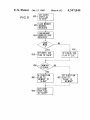
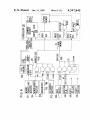
19
4,547,849
3. Record the current task as the slave microproces
20
1/0 READ, MEMORY WRITE
For this operation the master microprocessor per
forms an I/O Read cycle with the address bus equal to
the contents of the I/O address register (0000FCH), a
reversed [/0 address. The slave microprocessor re
sponds to this cycle by returning a data word to the
sor owner.
4. Use a SAVE ESC instruction to store slave micro
processor content in the old slave microprocessor
owner save area.
5. Use a RESTORE ESC instruction to load slave
microprocessor content from the new slave micro
processor owner save area.
master microprocessor over the data bus. The master
6. Return.
microprocessor then performs a memory write cycle
Since task switches may occur during execution of 10 which writes this data word into memory at the mem
the TS Trap Handler, it is advisable to make use of a
ory address indicated by the effective address of the
semaphore in order to execute Steps 3, 4, and 5 as a
ESC instruction (with normal segment translation as
critical region. Notice that Step 2 will provide for nest
speci?ed by the compatibility Mode/protection Mode
ing of the TS Trap Handler.
control).
The DNA trap leaves the return link pointing to the
?rst byte of the trapped instruction (or to the ?rst pre?x
SEND ESC
byte if any are present). Therefore, the return from trap
will cause restart of the trapped instruction. This time
For this operation the master microprocessor per
forms an I/O write cycle with address bus equal to
0000FCH, a reserved I/O address, and the data bus
equal to the ?rst two bytes of the ESC instruction.
TS will be reset so that the Tasked-Switched Test will
fail and the remaining operations of the ESC instruction
category will be executed.
SEND IP, CS
For this operation the master microprocessor per
forms two I/O write cycles with address bus equal to
OOOOFEH, a reserved I/O address. On the ?rst cycle the
data bus is equal the current value of the IP register (i.e,
the value corresponding to the ?rst byte of the ESC
instruction, or ?rst pre?x byte if any are present). On
IDLE ON BUSY
For this operation the master microprocessor tests
BUSY# from the slave microprocessor and waits until
the slave microprocessor indicates that it is not busy
before the master microprocessor proceeds to the next
operation of the particular category.
Whenever the slave microprocessor begins execution
the second cycle the data bus is equal to the current
of any ESC instruction except for those of Categories 4 30 contents of the CS register.
or 5, it will immediately indicate busy on its BUSY#
SEND EA, DS
pin. When the slave microprocessor completes the ESC
instruction, whether or not it results in an error, it will
For this operation the master microprocessor per
indicate not busy on its BUSY# pin. If the ESC instruc'
forms two I/O write cycles with the address bus equal
tion does result in an error, it will indicate error on its 35 to DUOOFEH, a reserved [/0 address. On the ?rst cycle
ERROR# pin for at least 100 ns before it indicates not
the data bus is equal to the effective address as speci?ed
busy on its BUSY# pin so that there is no interval in
by the second byte of the ESC instruction. On the sec
which it indicates not busy and no error.
ond cycle the data bus is equal to the current contents of
The master microprocessor is interruptable during
the DS register (or other segment register if a segment
this idling time. If an interrupt does occur, the return
override pre?x is used).
link will point to the first byte of the interrupted instruc
tion (or ?rst pre?x byte) so that the return from inter
1/0 READ TO AX
For this operation the master microprocessor per
forms an I/O Read cycle with address bus equal
rupt will cause restart of the instruction from the begin
mng.
LOAD DATA CHANNEL FOR SLAVE
45 0000FCI-I, a reserved I/O address. The slave micro
MICROPROCESSOR TRANSFERS TO/ FROM
MEMORY
The master microprocessor logic performs on auto
matic initialization of the Data Channel. The block 50
diagram of FIG. 6 shows the essential components of
the data channel. (see Coprocessor Data Channel sec
tion below). This initialization is illustrated by the logic
?ow chart of FIG. 5 and consists of:
processor responds to this command by returning a data
word to the master microprocessor over the data bus.
The master microprocessor accepts this data word and
places it in its AX register.
ESC INSTRUCTION DECODING
As the master microprocessor encounters ESC in
structions, it decodes each instruction into one of the
1. Setting the start/stop ?ag to "stop” (block 450).
eight categories given in the above ESC Instruction
Categories section and performs the operations required
2. Loading the memory address register (MAR) with
for that category. The format of the ESC instruction is:
the sum of the selected segment base and the effec
tive address as speci?ed by the mod, r/m byte of
the ESC instruction (block 452).
3. Loading the memory address limit register with the
sum of the base and limit for the selected segment
(block 454).
60
110 through 10 are mapped into the eight categories.
WAIT INSTRUCTION
4. Setting the user/ICE ?ag to “user mode" (block
456) or “ICE" mode (block 457).
Due to the Idle on Busy operation performed by the
5. Setting the direction flag to “memory to slave 65 master microprocessor on certain ESC instructions, the
microprocessor" (block 460) or "slave to memory"
WAIT instruction necessary for Intel 8086/8087 sys
(block 462).
tems is not always required for master microprocessor/
6. Setting the start/stop ?ag to “start" (464).
slave microprocessor operation. However, in order to


![[v0.3.5.63 Blue Release] (4.17MB PDF)](http://vs1.manualzilla.com/store/data/005758602_1-69f3b29a9a050ef0b6d8d37fccf12e09-150x150.png)