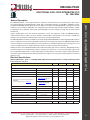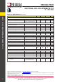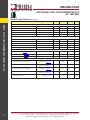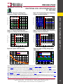
1
HMC832LP6GE v01.0812 FRACTIONAL-N PLL WITH INTEGRATED VCO 25 - 3000 MHz PLLS WITH INTEGRATED VCO - SMT Features 1 • RF Bandwidth: 25 - 3000 MHz • Fractional Figure of Merit (FOM) -226 dBc/Hz • 3.3 V Supply • Exact Frequency Mode with 0 Hz frequency error • Maximum Phase Detector Rate 100 MHz • Fast Frequency Hopping • Ultra Low Phase Noise -110 dBc/Hz in Band Typ. • 24-bit Step Size, Resolution 3 Hz typical • 40 Lead 6x6 mm SMT Package: 36 mm2 Typical Applications • Cellular Infrastructure • CATV Equipment • Microwave Radio • DDS Replacement • WiMax, WiFi • Military • Communications Test Equipment • Tunable Reference Source for Spurious-Free Performance Functional Diagram For price, delivery, and to place orders: Hittite Microwave Corporation, 2 Elizabeth Drive, Chelmsford, MA 01824 Phone: 978-250-3343 Fax: 978-250-3373 Order On-line at www.hittite.com Application Support: Phone: 978-250-3343 or [email protected] HMC832LP6GE v01.0812 FRACTIONAL-N PLL WITH INTEGRATED VCO 25 - 3000 MHz The HMC832LP6GE is a 3.3 V, high performance, wide-band, Fractional-N Phase-Locked-Loop (PLL) that features an integrated Voltage Controlled Oscillator (VCO) with a fundamental frequency of 1500 MHz - 3000 MHz, and an integrated VCO Output Divider (divide by 1/2/4/6.../60/62), that enables the HMC832LP6GE to generate continuous frequencies from 25 MHz to 3000 MHz. The integrated Phase Detector (PD) and delta-sigma modulator, capable of operating at up to 100 MHz, permit wider loop-bandwidths and faster frequency tuning, with excellent spectral performance. Industry leading phase noise and spurious performance, across all frequencies, enable the HMC832LP6GE to minimize blocker effects, improve receiver sensitivity and transmitter spectral purity. Low noise floor (-160 dBc/Hz) eliminates any contribution to modulator/mixer noise floor in transmitter applications. The HMC832LP6GE is footprint compatible to the market leading HMC830LP6GE PLL with Integrated VCO. It features all 3.3 V supply and an innovative Programmable Performance technology that enables the HMC832LP6GE to tailor current consumption and corresponding noise floor performance to individual applications by selecting either a low current consumption mode, or a high performance mode for an improved noise floor performance. Additional features of the HMC832LP6GE include 12 dB of RF output gain control in 1 dB steps; Output Mute function to automatically mute the output during frequency changes when the device is not locked; Selectable output return loss; Programmable differential or single-ended outputs, with the ability to select either output in single-ended mode; and a delta-sigma modulator Exact Frequency Mode which enables users to generate output frequencies with 0 Hz frequency error. Electrical Specifications VPPCP, VDDLS, VCC1, VCC2 = 3.3 V; RVDD, AVDD, DVDD, VCCPD, VCCHF, VCCPS = 3.3 V Min and Max Specified across Temp -40 °C to 85 °C Parameter Condition Min. Typ. Max. Units 25 3000 MHz VCO Frequency at PLL Input 1500 3000 MHz RF Output Frequency at f VCO 1500 3000 MHz RF Output Characteristics Output Frequency PLLS WITH INTEGRATED VCO - SMT General Description Output Power Max Gain Setting VCO_Reg 07h[3:0]=11d Single-Ended 7 Gain setting 6 VCO_Reg 07h[3:0]=6d Differential 2 1 dB Steps 12 dB fo Mode at 2 GHz 2nd / 3rd / 4th -20/-29/-45 dBc fo/2 Mode at 2GHz/2 = 1 GHz 2nd / 3rd / 4th -26/-10/-34 dBc fo/30 Mode at 3 GHz/30 = 100 MHz 2nd / 3rd / 4th -33/-10/-40 dBc fo/62 Mode at 1550 MHz/62 = 25 MHz 2nd / 3rd / 4th -40/-6/-43 dBc RF Output Power at fundmental frequency = 2000 MHz Across all Frequencies see Figure 22 Output Power Control range dBm Harmonics for Fundamental Mode VCO Output Divider VCO RF Divider Range 1,2,4,6,8,...,62 1 62 For price, delivery, and to place orders: Hittite Microwave Corporation, 2 Elizabeth Drive, Chelmsford, MA 01824 Phone: 978-250-3343 Fax: 978-250-3373 Order On-line at www.hittite.com Application Support: Phone: 978-250-3343 or [email protected] 2 HMC832LP6GE v01.0812 FRACTIONAL-N PLL WITH INTEGRATED VCO 25 - 3000 MHz PLLS WITH INTEGRATED VCO - SMT Electrical Specifications (Continued) Parameter Condition Min. Typ. Max. Max = 219 - 1 16 524,287 Fractional nominal divide ratio varies (+/- 4) dynamically max 20 524,283 Units PLL RF Divider Characteristics 19-Bit N-Divider Range (Integer) 19-Bit N-Divider Range (Fractional) REF Input Characteristics Max Ref Input Frequency Ref Input Level AC Coupled [1] -6 Ref Input Capacitance 14-Bit R-Divider Range Phase Detector (PD) 350 MHz 12 dBm 5 pF 1 16,383 DC 100 MHz DC 100 MHz 2.54 mA [2] PD Frequency Fractional Mode [3] PD Frequency Integer Mode Charge Pump Output Current 0.02 Charge Pump Gain Step Size PD/Charge Pump SSB Phase Noise 20 µA -143 dBc/Hz 50 MHz Ref, Input Referred 1 kHz 10 kHz Add 2 dB for Fractional -150 dBc/Hz 100 kHz Add 3 dB for Fractional -152 dBc/Hz Logic Inputs Vsw 40 50 60 % DVDD Logic Outputs VOH Output High Voltage DVDD VOL Output Low Voltage V 0 Output Impedance 100 Maximum Load Current V 200 Ω 1.5 mA 3.5 V Power Supply Voltages 3.3 V Supplies AVDD, VCCHF, VCCPS, VCCPD, RVDD,DVDD, VPPCP, VDDLS, VCC1, VCC2 3.1 3.3 [1] Measured with 100 Ω external termination. See “Reference Input Stage” section for more details. [2] Slew rate of ≥ 0.5 ns/V is recommended, see “Reference Input Stage” section for more details. Frequency is guaranteed across process voltage and temperature from -40 °C to +85 °C. [3] This maximum PD frequency can only be achieved if the minimum N value is respected. eg. In the case of fractional mode, the maximum PD frequency = fvco/20 or 100 MHz, whichever is less. 3 For price, delivery, and to place orders: Hittite Microwave Corporation, 2 Elizabeth Drive, Chelmsford, MA 01824 Phone: 978-250-3343 Fax: 978-250-3373 Order On-line at www.hittite.com Application Support: Phone: 978-250-3343 or [email protected] HMC832LP6GE v01.0812 FRACTIONAL-N PLL WITH INTEGRATED VCO 25 - 3000 MHz Parameter Condition Min. Typ. Max. Units Power Supply Currents Gain 11 (VCO_Reg 07h[3:0] = 11d) Single-Ended Output 2500 MHz 219 800 MHz 230 Gain 6 (VCO_Reg 07h[3:0] = 6d) Differential Output 2500 MHz 226 (VCO_Reg 03h[3:2] = 3d) 800 MHz 237 Gain 1 (VCO_Reg 07h[3:0] = 1d) Differential Output 2500 MHz 210 VCO_Reg 03h[3:2] = 3d 800 MHz 221 Gain 6 (VCO_Reg 07h[3:0] = 6d) Differential Output 2500 MHz 195 (VCO_Reg 03h[3:2] = 3d) 800 MHz 205 Gain 1 VCO_Reg 07h[3:0] = 1d Differential Output 2500 MHz 180 800 MHz 192 (VCO_Reg 03h[3:2] = 2d) High Performance Mode (VCO_Reg 03h[1:0] =3d) [4] Low Current Mode (VCO_Reg 03h[1:0] =3d) [4] VCO_Reg 03h[3:2] = 3d Power Down - Crystal Off Power Down - Crystal On, 100 MHz mA mA Reg 01h=0, Crystal Not Clocked 10 µA Reg 01h=0, Crystal Clocked 100 MHz 5 mA 700 mV PLLS WITH INTEGRATED VCO - SMT Electrical Specifications (Continued) Power on Reset Typical Reset Voltage on DVDD Min DVDD Voltage for No Reset 1.5 Power on Reset Delay V 250 µs 10 kHz Offset -88 dBc/Hz 100 kHz Offset -116 dBc/Hz 1 MHz Offset -139 dBc/Hz 10 MHz Offset -157 dBc/Hz 100 MHz Offset -162 dBc/Hz VCO Open Loop Phase Noise at fo @ 2 GHz [5] [4] For detailed current consumption information please refer to Figure 31, and Figure 32. [5] Gain setting = 6 (VCO_Reg 07h[3:0] = 6d) in High Performance mode (VCO_Reg 03h[1:0] = 3d). For price, delivery, and to place orders: Hittite Microwave Corporation, 2 Elizabeth Drive, Chelmsford, MA 01824 Phone: 978-250-3343 Fax: 978-250-3373 Order On-line at www.hittite.com Application Support: Phone: 978-250-3343 or [email protected] 4 HMC832LP6GE v01.0812 FRACTIONAL-N PLL WITH INTEGRATED VCO 25 - 3000 MHz Electrical Specifications (Continued) PLLS WITH INTEGRATED VCO - SMT Parameter VCO Open Loop Phase Noise at fo @ 2 GHz/2 = 1 GHz Min. Typ. Max. Units [5] 10 kHz Offset -93 dBc/Hz 100 kHz Offset -122 dBc/Hz 1 MHz Offset -145 dBc/Hz 10 MHz Offset -159 dBc/Hz 100 MHz Offset -162 dBc/Hz 10 kHz Offset -110 dBc/Hz 100 kHz Offset -139 dBc/Hz 1 MHz Offset -160 dBc/Hz 10 MHz Offset -163 dBc/Hz 100 MHz Offset -163 dBc/Hz VCO Open Loop Phase Noise at fo @3 GHz/30 = 100 MHz [5] Figure of Merit (FOM) Floor Integer Mode (Figure 20) Normalized to 1 Hz -229 dBc/Hz Floor Fractional Mode (Figure 20) Normalized to 1 Hz -226 dBc/Hz Flicker (Both Modes) (Figure 20) Normalized to 1 Hz -268 dBc/Hz VCO Tuning Sensitivity at 2800 MHz Measured with 1.5 V on VTUNE; see Figure 29 24.6 MHz/V VCO Tuning Sensitivity at 2400 MHz Measured with 1.5 V on VTUNE; see Figure 29 25.8 MHz/V VCO Tuning Sensitivity at 2000 MHz Measured with 1.5 V on VTUNE; see Figure 29 25.2 MHz/V VCO Tuning Sensitivity at 1600 MHz Measured with 1.5 V on VTUNE; see Figure 29 24.3 MHz/V Measured with 1.5 V on VTUNE 2.8 MHz/V VCO Characteristics VCO Supply Pushing 5 Condition For price, delivery, and to place orders: Hittite Microwave Corporation, 2 Elizabeth Drive, Chelmsford, MA 01824 Phone: 978-250-3343 Fax: 978-250-3373 Order On-line at www.hittite.com Application Support: Phone: 978-250-3343 or [email protected] HMC832LP6GE v01.0812 FRACTIONAL-N PLL WITH INTEGRATED VCO 25 - 3000 MHz Typical Performance Characteristics -100 -100 -110 Loop BW = 75 kHz PHASE NOISE (dBc/Hz) PHASE NOISE (dBc/Hz) -110 -120 -130 Loop BW = 127 kHz -140 -150 750 MHz, EVM = -62.5dB, or 0.075 % 1600 MHz, EVM = -57dB or 0.141% 2500 MHz, EVM = -53.3dB or 0.216% 875 MHz, EVM = -64.8dB or 0.058% 1600 MHz, EVM = -59.8dB or 0.102% 2500MHz, EVM = -55.8dB or 0.168% -160 -170 3 10 10 4 10 5 -120 Loop BW = 127 kHz -130 Loop BW = 75 kHz -140 -150 880 MHz, EVM = -61.3 dB or 0.086% 1605 MHz, EVM = -57.5 dB or 0.133% 2505 MHz, EVM = -52 dB or 0.251% 880 MHz, EVM = -61.8 dB or 0.081% 1605MHz, EVM = -57.2 dB or 0.138% 2505 MHz, EVM = -53.9 dB or 0.204% -160 10 6 10 7 10 -170 3 10 8 10 4 10 OFFSET (Hz) 5 10 6 10 7 10 8 10 8 OFFSET (Hz) Figure 4. Closed Loop Phase Noise at 1800 MHz, Divided by 1 to 62 [2] Figure 3. Open Loop VCO Phase Noise at 1800 MHz -100 -60 -110 PHASE NOISE (dBc/Hz) -80 PHASE NOISE (dBc/Hz) PLLS WITH INTEGRATED VCO - SMT Figure 2. Typical Closed Loop Fractional Phase Noise [1] Figure 1. Typical Closed Loop Integer Phase Noise [1] -100 -120 Low Current Mode (VCO_Reg03h[10]=1d) -140 -120 /1 /2 /4 -130 /8 /16 -140 /32 -150 /62 -160 -180 3 10 -160 High Performance Mode (VCO_Reg03h[10]=3d) 10 4 10 5 10 6 10 7 10 -170 3 10 8 10 4 10 5 10 6 10 7 OFFSET (Hz) OFFSET (Hz) Figure 6. Closed Loop Phase Noise at 3000 MHz, Divided by 1 to 62 [2] Figure 5. Free Running VCO Phase Noise at 3000 MHz -40 -100 -60 -110 PHASE NOISE (dBc/Hz) PHASE NOISE (dBc/Hz) /1 -80 -100 -120 Low Current Mode (VCO_Reg03h[10]=1d) -140 High Performance Mode (VCO_Reg03h[10]=3d) -160 -180 3 10 10 4 10 5 10 OFFSET (Hz) 6 /2 -120 /4 -130 /16 /8 -140 -150 /32 /62 -160 10 7 10 8 -170 3 10 10 4 10 5 10 6 10 7 10 8 OFFSET (Hz) [1] Measured with 50 MHz PD frequency, output gain of 6 (VCO_Reg 07h[3:0] = 6d) and in High Performance Mode (VCO_Reg 03h[1:0] = 3d). Loop Filter designs are provided in Table 1. Phase Noise integrated from 1 kHz to 100 MHz. [2] PD frequency, loop filter bandwidth 75 kHz (Type 2 from Table 1), Only a subset of available output divide ratios is shown. Full range of output divide values includes 1,2,4,6,8, ... 58, 60, 62 . High Performance Mode selected (VCO_Reg 03h[1:0] = 3d). For price, delivery, and to place orders: Hittite Microwave Corporation, 2 Elizabeth Drive, Chelmsford, MA 01824 Phone: 978-250-3343 Fax: 978-250-3373 Order On-line at www.hittite.com Application Support: Phone: 978-250-3343 or [email protected] 6 HMC832LP6GE v01.0812 FRACTIONAL-N PLL WITH INTEGRATED VCO 25 - 3000 MHz Figure 7. Fractional Spurious Performance at 904 MHz, Exact Frequency Mode ON [3] Figure 8. Fractional Spurious Performance at 1804 MHz, Exact Frequency Mode ON [4] -60 -80 Low Current Mode (VCO_Reg03h[10]=1d) SSB Integrated Phase Noise = -64.3 dBc Integration Bandwidth = 1 kHz to 100 MHz SNR = 61.3, EVM = 0.086 %, Phase Noise Integration Bandwidth 1 kHz to 100 MHz -100 PHASE NOISE (dBc/Hz) PHASE NOISE (dBc/Hz) -80 -120 -140 High Performance Mode (VCO_Reg03h[10]=3d) SSB Integrated Phase Noise = -65.5 dBc Integration Bandwidth = 1 kHz to 100 MHz SNR = 62.5 dB, EVM = 0.075 % Phase Noise Integration Bandwidth 1 kHz to 100 MHz -160 -180 10 3 10 4 10 5 10 6 Low Current Mode (VCO_Reg03h[10]=1d) SSB Integrated Phase Noise = -58.7 dBc Integration Bandwidth = 1 kHz to 100 MHz SNR = 55.7, EVM = 0.164 %, Phase Noise Integration Bandwidth 1 kHz to 100 MHz -100 -120 -140 High Performance Mode (VCO_Reg03h[10]=3d) SSB Integrated Phase Noise = -59 dBc Integration Bandwidth = 1 kHz to 100 MHz SNR = 56 dB, EVM = 0.158 %, Phase Noise Integration Bandwidth 1 kHz to 100 MHz -160 -180 10 7 10 8 10 3 10 4 Figure 9. Fractional Spurious Performance at 2118.24 MHz, Exact Frequency Mode ON[5] 6 10 7 10 8 -100 -120 -140 High Performance Mode (VCO_Reg03h[10]=3d) SSB Integrated Phase Noise = -57.45 dBc Integration Bandwidth = 1 kHz to 100 MHz SNR = 54.45 dB, EVM = 0.189 %,Phase Noise Integration Bandwidth 1 kHz to 100 MHz -160 10 3 10 4 10 5 10 6 Low Current Mode (VCO_Reg03h[10]=1d) SSB Integrated Phase Noise = -57 dBc Integration Bandwidth = 1 kHz to 100 MHz SNR = 54, EVM = 0.199 %, Phase Noise Integration Bandwidth 1 kHz to 100 MHz -80 PHASE NOISE (dBc/Hz) -80 -100 -120 -140 High Performance Mode (VCO_Reg03h[10]=3d) SSB Integrated Phase Noise = -57.45 dBc Integration Bandwidth = 1 kHz to 100 MHz SNR = 54.45 dB, EVM = 0.189 %,Phase Noise Integration Bandwidth 1 kHz to 100 MHz -160 -180 10 7 10 8 10 3 10 4 OFFSET (Hz) 10 5 10 6 10 7 10 8 OFFSET (Hz) Figure 11. Fractional Spurious Performance at 2646.96 MHz, Exact Frequency Mode ON [7] Figure 12. Fractional Spurious Performance at 2646.96 MHz, Exact Frequency Mode OFF [8] -60 -60 Low Current Mode (VCO_Reg03h[10]=1d) SSB Integrated Phase Noise = -55.6 dBc Integration Bandwidth = 1 kHz to 100 MHz SNR = 52.6, EVM = 0.234 %, Phase Noise Integration Bandwidth 1 kHz to 100 MHz -100 -120 -140 High Performance Mode (VCO_Reg03h[10]=3d) SSB Integrated Phase Noise = -56 dBc Integration Bandwidth = 1 kHz to 100 MHz SNR = 53 dB, EVM = 0.224 %, Phase Noise Integration Bandwidth 1 kHz to 100 MHz -160 -180 Low Current Mode (VCO_Reg03h[10]=1d) SSB Integrated Phase Noise = -55.6 dBc Integration Bandwidth = 1 kHz to 100 MHz SNR = 52.6, EVM = 0.234 %, Phase Noise Integration Bandwidth 1 kHz to 100 MHz -80 PHASE NOISE (dBc/Hz) -80 PHASE NOISE (dBc/Hz) 10 -60 Low Current Mode (VCO_Reg03h[10]=1d) SSB Integrated Phase Noise = -57 dBc Integration Bandwidth = 1 kHz to 100 MHz SNR = 54, EVM = 0.199 %, Phase Noise Integration Bandwidth 1 kHz to 100 MHz -180 -100 -120 -140 High Performance Mode (VCO_Reg03h[10]=3d) SSB Integrated Phase Noise = -56 dBc Integration Bandwidth = 1 kHz to 100 MHz SNR = 53 dB, EVM = 0.224 %, Phase Noise Integration Bandwidth 1 kHz to 100 MHz -160 -180 3 10 4 10 5 10 6 10 7 10 8 10 3 10 4 OFFSET (Hz) [3] 122.88 MHz Xtal, PFD = 61.44 MHz, Channel Spacing = 200 KHz, Loop Filter Type 2 from Table 1. [4] 122.88 MHz Xtal, PFD = 61.44 MHz, Channel Spacing = 200 KHz, Loop Filter Type 2 from Table 1. [5] 122.88 MHz Xtal, PFD = 61.44 MHz, Channel Spacing = 240 KHz, Loop Filter Type 2 from Table 1. [6] Identical configuration to [5] with Exact Frequency Mode turned Off. [7] 122.88 MHz Xtal, PFD = 61.44 MHz, Channel Spacing = 240 KHz, Loop Filter Type 2 from Table 1. [8] Identical configuration to [7] with Exact Frequency Mode turned Off. 7 5 Figure 10. Fractional Spurious Performance at 2118.24 MHz, Exact Frequency Mode OFF [6] -60 10 10 OFFSET (kHz) OFFSET (Hz) PHASE NOISE (dBc/Hz) PLLS WITH INTEGRATED VCO - SMT -60 10 5 10 6 10 7 10 8 OFFSET (Hz) For price, delivery, and to place orders: Hittite Microwave Corporation, 2 Elizabeth Drive, Chelmsford, MA 01824 Phone: 978-250-3343 Fax: 978-250-3373 Order On-line at www.hittite.com Application Support: Phone: 978-250-3343 or [email protected] HMC832LP6GE v01.0812 FRACTIONAL-N PLL WITH INTEGRATED VCO 25 - 3000 MHz Figure 13. Low Frequency Performance [9] -120 Figure 14. Typical Spurious Emissions at 2000.1 MHz, Fixed Reference [10] -80 PHASE NOISE (dBc/Hz) PHASE NOISE (dBc/Hz) -130 -140 100 MHz Output -150 55.55 MHz Output -160 -120 -140 -160 25 MHz Output -170 2 10 -100 -180 10 3 10 4 10 5 10 6 10 7 10 8 10 3 10 4 10 OFFSET (Hz) -60 -60 -80 -70 -100 -120 -140 6 10 7 10 8 -80 Typical Spurios vs Offset from 2 GHz, Fixed Reference = 50 MHz -90 -100 Typical Spurious vs Offset from 2 GHz, Tunable Reference ~47.5 MHz -110 -160 -120 2000.010 10 -180 3 10 4 10 5 10 6 10 7 10 8 OFFSET (Hz) 2001 1000 -100 -40 High Performance Mode On (VCO_Reg-3h[1:0] = 3d) 27C -40C 85C -110 -80 PHASE NOISE (dBc/Hz) -60 2000.100 100 OUTPUT FREQUENCY (kHz) Figure 18. Open Loop Phase Noise vs. Temp. Figure 17. Open Loop Phase Noise PHASE NOISE (dBc/Hz) 10 Figure 16. Typical Spurious vs Offset from 2 GHz, Fixed vs. Tunable Reference [12] PHASE NOISE (dBc/Hz) PHASE NOISE (dBc/Hz) Figure 15. Typical Spurious Emissions at 2000.1 MHz,Tunable Reference [11] 10 5 OFFSET (Hz) PLLS WITH INTEGRATED VCO - SMT -60 2854 MHz 2453 MHz 2013 MHz 1587 MHz -100 -120 -140 -160 100 kHz Offset All Modes -120 1 MHz Offset All Modes -130 -140 Low Current Mode -150 -160 High Performance Mode -180 3 10 10 4 10 5 10 OFFSET (Hz) 6 10 7 10 8 100 MHz Offset -170 30 100 300 1000 FREQUENCY (MHz) [9] 100 MHz Xtal, PD Frequency = 50 MHz, loop filter bandwidth 75 kHz (Type 2 from Table 1), Fractional Mode. 50 MHz Low Pass Filter used at the output of the HMC832LP6GE only for the 25 MHz curve. Charge Pump is set to Maximum value. [10] 50 MHz fixed reference, 50 MHz PD frequency. The plot shows an integer boundary spur inside the loop filter bandwidth. All PLLs with Integrated VCOs exhibit integer boundary spurs at harmonics of the reference frequency. The plot shows the worst case spurious scenario where harmonic of the reference frequency (50 MHz) is within the loop filter bandwidth of the fundamental frequency of the HMC832LP6GE. [11] Loop Filter Type 2 from Table 1. The tunable reference is used to change the reference frequency from 50 MHz in Figure 14 to 47.5 MHz in figure Figure 15 in order to distance the harmonic of the reference frequency (spurious emissions) away from the fundamental output frequency of the HMC832LP6GE so that it is filtered by the loop filter. The internal HMC832LP6GE setup and divide ratios are changed in the opposite direction accordingly so that the HMC832LP6GE generates identical output frequency as in Figure 14 without the spurious emissions inside the loop bandwidth. [12] The graph is generated by observing, and plotting, the magnitude of only the largest spur, at any offset, at each output frequency, while using a fixed 50 MHz reference and a tunable 47.5 MHz reference, and following procedure discussed in [11]. See HMC832LP6GE Application Information section for more details. Contact Hittite Apps Support to obtain the required configuration to achieve similar spurious performance throughout the operating range of the HMC832LP6GE. For price, delivery, and to place orders: Hittite Microwave Corporation, 2 Elizabeth Drive, Chelmsford, MA 01824 Phone: 978-250-3343 Fax: 978-250-3373 Order On-line at www.hittite.com Application Support: Phone: 978-250-3343 or [email protected] 8 HMC832LP6GE v01.0812 FRACTIONAL-N PLL WITH INTEGRATED VCO 25 - 3000 MHz Figure 19. Single Sideband Integrated Phase Noise, High Performance Mode [13] -55 Phase Noise Integrated from 10 kHz to 20 MHz -60 0.141 -65 -70 0.0447 -75 -40C 27C 85C -80 0.0141 -85 NORMALIZED PHASE NOISE (dBc/Hz) SSB INTEGRATED PHASE NOISE (dBc) -200 0.446 EVM (%) -210 Typ FOM vs Offset -220 FOM Floor FOM 1/f Noise -230 -240 2 10 0.0045 -90 100 1000 10 3 10 4 Figure 21. Typical Single-Ended Output Power vs Frequency (Mid Gain Setting 6) 5 10 6 Figure 22. Typical Output Power vs Frequency and Gain (Single-Ended) 15 20 Gain Setting = 11 (VCO_Reg07h[3:0] = 11d) 15 10 OUTPUT POWER (dBm) High Performance Mode (VCO_Reg03h[1:0] = 3d) 5 0 Return Loss (VCO_Reg03h[5] = 0) -5 Return Loss (VCO_Reg03h[5] = 1) 10 5 0 Gain Setting = 5 (VCO_Reg07h[3:0] = 5d) -5 Gain Setting = 0 (VCO_Reg07h[3:0] = 0d) -10 -10 Low Current Mode Low Current Mode (VCO_Reg03h[1:0] = 1d) -15 100 1000 -15 3000 High Performance Mode -20 100 FRQUENCY (MHz) 1000 3000 FRQUENCY (MHz) Figure 23. Typical RF Output Power at 2 GHz (Single-Ended) vs. Temperature Figure 24. RF Output Return Loss 0 10 Return Loss 0 (VCO_Reg03h[5] = 0) 8 -5 27C 6 -40C RETURN LOSS (dB) OUTPUT POWER (dBm) 10 OFFSET (Hz) OUTPUT FREQUENCY (MHz) OUTPUT POWER (dBm) PLLS WITH INTEGRATED VCO - SMT -50 Figure 20. Figure of Merit 85C 4 2 0 -10 Return Loss 1 (VCO_Reg03h[5] = 1) -15 -20 -2 -25 -4 -30 -6 0 2 4 6 GAIN SETTING 8 10 100 1000 OUTPUT FREQUENCY (MHz) [13] Loop Filter Type 2 from Table 1 used. [14] Using High Performance Mode (VCO_Reg 03h[1:0] = 3d) [15] The HMC832LP6GE features programmable RF Output Return loss (VCO_Reg 03h[5]) and 12 dB of programmable gain (VCO_Reg 07h[3:0]). Maximum output power is achieved with high Return Loss setting (VCO_Reg 03h[5] = 0) as shown in Figure 21. Setting VCO_Reg 03h[5] = 1 improves Return Loss for applications that require it (Figure 21), at the cost of reduced RF Output Power (Figure 24). 9 For price, delivery, and to place orders: Hittite Microwave Corporation, 2 Elizabeth Drive, Chelmsford, MA 01824 Phone: 978-250-3343 Fax: 978-250-3373 Order On-line at www.hittite.com Application Support: Phone: 978-250-3343 or [email protected] HMC832LP6GE v01.0812 FRACTIONAL-N PLL WITH INTEGRATED VCO 25 - 3000 MHz Figure 25. Frequency Settling After Frequency Change, AutoCal Enabled [16] Figure 26. Phase Settling After Frequency Change, AutoCal Enabled [16] Settling Time to < 10 Degrees Phase Error PHASE ERROR (DEGREES) FREQUENCY ERROR (GHz) 150 Settling Time to < 10 Degrees Phase Error 3 2.8 2.6 100 50 0 -50 -100 2.4 -150 2.2 0 20 40 60 80 100 120 140 -200 160 0 20 Figure 27. Frequency Settling After Frequency Change, Manual Calibration [17] PHASE ERROR (DEGREES) FREQUENCY ERROR (GHz) 80 100 120 140 160 200 Settling Time to < 10 Degrees Phase Error 150 Settling Time to < 10 Degrees Phase Error 2.505 2.5 Note: Loop Filter Bandwidth = 127 kHz, Loop Filter Phase Margin = 61 degrees.This result is directly affected by loop filter design. Faster settling time is possilbe with wider loop filter bandwidth and higher phase margin. 100 50 0 -50 -200 0 20 40 60 80 100 120 140 Note: Loop Filter Bandwidth = 127 kHz, Loop Filter Phase Margin = 61 degrees.This result is directly affected by loop filter design. Faster settling time is possilbe with wider loop filter bandwidth and higher phase margin. -100 -150 160 0 20 40 60 80 100 120 140 160 TIME (us) TIME (us) Figure 30. Typical Tuning Voltage After Calibration [15] Figure 29. Typical VCO Sensitivity 4 TUNE VOLTAGE AFTER CALIBRATION (V) 90 2854 MHz, Tuning Cap 15 2453 MHz, Tuning Cap 15 2013 MHz, Tuning Cap 15 1587 MHz, Tuning Cap 15 80 70 kVCO (MHz/V) 60 Figure 28. Phase Settling After Frequency Change, Manual Calibration [17] 2.51 2.495 40 TIME (uS) TIME (us) PLLS WITH INTEGRATED VCO - SMT 200 3.2 60 50 40 30 20 10 0 0.66 1.3 2 TUNING VOLTAGE (V) 2.6 3.3 Calibrated at 85C, measured at 85C Calibrated at 85, measured at -40C Calibrated at -40C,measured at -40C Calibrated at -40C,measured at 85C Calibrated at 27C, measured at 27C 3.5 3 2.5 2 1.5 1 0.5 0 fmin fmax 1330 1520 1710 1900 2090 2280 2470 2660 2850 3040 VCO FREQUENCY(MHz) [16] The HMC832LP6GE features an internal AutoCal process that seamlessly calibrates the HMC832LP6GE when a frequency change is executed. Typical frequency settling time that can be expected after any frequency change (Reg 03h or Reg 04h writes) is shown in Figure 25 with AutoCal enabled (Reg 0Ah[11] = 0). Frequency hop of 5 MHz is shown in Figure 25, however the settling time is independent of the size of the frequency change. Any size frequency size hop will have a similar settling time with AutoCal enabled. Loop filter BW = 127 kHz (Type 1 in Table 1). [17] For applications that require fast frequency changes, the HMC832LP6GE supports manual calibration that enables faster settling times. Manual calibration needs to be executed only once for each individual HMC832LP6GE, at any temperature, and is valid across all temperature operating range of the HMC832LP6GE. More information about manual calibration is available in section 1.4.1.6. Frequency hop of 5 MHz is shown in Figure 27 and Figure 28 however the settling time is independent of the size of the frequency change. Any size frequency size hop will have a similar settling time with AutoCal disabled (Reg 0Ah[11] = 1). Loop filter BW = 127 kHz (Type 1 in Table 1). [18] The HMC832LP6GE features an internal AutoCal process that seamlessly calibrates the HMC832LP6GE when a frequency change is executed. Once calibrated, at any temperature, the calibration setting holds across the entire operating range of the HMC832LP6GE (-40 °C to +85 °C). Figure 30 shows that the tuning voltage of the HMC832LP6GE is maintained within a narrow operating range for worst case scenarios where calibration was executed at one temperature extreme and the HMC832LP6GE is operating at the other extreme. For price, delivery, and to place orders: Hittite Microwave Corporation, 2 Elizabeth Drive, Chelmsford, MA 01824 Phone: 978-250-3343 Fax: 978-250-3373 Order On-line at www.hittite.com Application Support: Phone: 978-250-3343 or [email protected] 10 HMC832LP6GE v01.0812 FRACTIONAL-N PLL WITH INTEGRATED VCO 25 - 3000 MHz Figure 31. Current Consumption in SingleEnded Output Configuration [19] Figure 32. Current Consumption in Differential Output Configuration [19] 260 Fo/62 Fo/62 - - - - - Output Gain 0 dB Output Gain 6 dB Fo/4 Fo/2 220 High Performance Mode (VCO_Reg03h[1:0] = 3d) Fo 210 200 190 Low Current Consumption Mode (VCO_Reg03h[1:0] = 1d) 180 - - - - - Output Gain 0 dB Fo/4 CURRENT CONSUMPTION (mA) CURRENT CONSUMPTION (mA) 230 170 Output Gain 6 dB Fo/2 240 Fo High Performance Mode (VCO_Reg03h[1:0] = 3d) 220 200 Low Current Consumption Mode (VCO_Reg03h[1:0] = 1d) 180 160 500 1000 1500 2000 2500 3000 500 1000 OUTPUT FREQUENCY (MHz) 232 230 230 225 228 220 FOM (dBc/Hz) 235 226 14 MHz Square Wave 25 MHz Square Wave 50 MHz Square Wave 100 MHz Square Wave 222 220 -15 2000 2500 3000 Figure 34. Reference Input Sensitivity, Sinusoidal Wave [20] 234 224 1500 OUTPUT FREQUENCY (MHz) Figure 33. Reference Input Sensitivity, Square Wave [20] FOM (dBc/Hz) PLLS WITH INTEGRATED VCO - SMT 240 215 14 MHz sin 25 MHz sin 50 MHz sq 100 MHz sq 210 205 200 -12 -9 -6 -3 0 3 REFERENCE POWER (dBm) -20 -15 -10 -5 0 5 REFERENCE POWER (dBm) Figure 35. Mute Mode Isolation [21] -10 ISOLATION (dB) -30 -50 Signal on RF_N pin when RF_N pin Off, RF_P pin On (VCO_Reg3h[3:2] = 1d), Mute Off (On only during VCO Calibration VCO_Reg03h[8:7] = 1d) Both RF_N & RF_P pins Off, (VCO_Reg3h[3:2] = 0d), Mute Off (On only during VCO Calibration VCO_Reg03h[8:7] = 1d) -70 -90 Mute On (VCO_Reg03h[8:7] = 3d) -110 100 1000 3000 FRQUENCY (MHz) [19] Output Gain is configured in VCO_Reg 07h[3:0]. Differential or single-ended mode programmed in VCO_Reg 03h[3:2]. [20] Measured from a 50 Ω source with a 100 Ω external resistor termination. [21] The HMC832LP6GE features a configurable mute mode, along with the ability to independently turn off outputs on both RF_N and RF_P output pins. Figure 35 shows isolation measured at the output when the mute mode is on (VCO_Reg 03h[8:7] = 3d), and when the mute mode is off (VCO_ Reg 03h[8:7] = 1d) with either both outputs disabled (VCO_Reg 03h[3:2] = 0), or one output enabled and the other disabled (VCO_Reg 03h[3:2] = 1d). 11 For price, delivery, and to place orders: Hittite Microwave Corporation, 2 Elizabeth Drive, Chelmsford, MA 01824 Phone: 978-250-3343 Fax: 978-250-3373 Order On-line at www.hittite.com Application Support: Phone: 978-250-3343 or [email protected] HMC832LP6GE v01.0812 FRACTIONAL-N PLL WITH INTEGRATED VCO 25 - 3000 MHz Loop Filter BW (kHz) Loop Filter Type Type 1 [22] Type 2 [23] Loop Filter Phase Margin C1 (pF) C2 (nF) C3 (pF) C4 (pF) R2 (Ω) R3 (Ω) R4 (Ω) 127 61° 390 10 82 82 750 300 300 75 61° 270 27 200 390 430 390 390 Loop Filter Design [22] Loop Filter Type 1 is suggested to use for best integrated phase noise. It is designed for 50 MHz PD frequency, CP =2 mA in Fractional Mode. [23] Loop Filter Type 2 is suggested to use for best far out phase noise. It is designed for 50 MHz PD frequency, CP =2 mA in Fractional Mode. Pin Descriptions Pin Number Function Description 1 AVDD DC Power Supply for analog circuitry. 2, 5, 6, 8, 9, 11 - 14, 18 - 22, 24, 26, 34, 37, 38 NC The pins are not connected internally; however. It is recommended to connect these pins to RF/DC ground externally. 3 VPPCP Power Supply for charge pump analog section 4 CP Charge Pump Output 7 VDDLS Power Supply for the charge pump digital section 10 RVDD Reference Supply 15 XREFP Reference Oscillator Input 16 DVDD DC Power Supply for Digital (CMOS) Circuitry 17 CEN PLL Subsystem Enable (No effect on the VCO Subsystem). Connect to logic high for normal operation. 23 VTUNE VCO Varactor. Tuning Port Input. 25 VCC2 VCO Analog Supply 2 27 VCC1 VCO Analog Supply 1 28 RF_N RF Negative Output 29 RF_P RF Positive Output 30 SEN PLL Serial Port Enable (CMOS) Logic Input 31 SDI PLL Serial Port Data (CMOS) Logic Input 32 SCK PLL Serial Port Clock (CMOS) Logic Input 33 LD/SDO Lock Detect, or Serial Data, or General Purpose (CMOS) Logic Output (GPO) 35 VCCHF DC Power Supply for Analog Circuitry 36 VCCPS DC Power Supply for Analog Prescaler 39 VCCPD DC Power Supply for Phase Detector 40 BIAS External bypass decoupling for precision bias circuits. Note: 1.920V ±20mV reference voltage (BIAS) is generated internally and cannot drive an external load. Must be measured with 10GΩ meter such as Agilent 34410A, normal 10MΩ DVM will read erroneously. For price, delivery, and to place orders: Hittite Microwave Corporation, 2 Elizabeth Drive, Chelmsford, MA 01824 Phone: 978-250-3343 Fax: 978-250-3373 Order On-line at www.hittite.com Application Support: Phone: 978-250-3343 or [email protected] PLLS WITH INTEGRATED VCO - SMT Table 1. Loop Filter Designs Used in Typical Performance Characteristics Graphs 12 HMC832LP6GE v01.0812 FRACTIONAL-N PLL WITH INTEGRATED VCO 25 - 3000 MHz PLLS WITH INTEGRATED VCO - SMT Absolute Maximum Ratings 13 AVDD, RVDD, DVDD, VCCPD, VCCHF, VCCPS -0.3 V to +3.6 V VPPCP, VDDLS, VCC1 -0.3 V to +3.6 V VCC2 -0.3 V to +3.6 V Operating Temperature -40 °C to +85 °C Storage Temperature -65 °C to 150 °C Maximum Junction Temperature 150 °C Thermal Resistance (ѲJC) (junction to case (ground paddle)) 9 °C/W Stresses above those listed under Absolute Maximum Ratings may cause permanent damage to the device. This is a stress rating only; functional operation of the device at these or any other conditions above those indicated in the operational section of this specification is not implied. Exposure to absolute maximum rating conditions for extended periods may affect device reliability. Reflow Soldering Peak Temperature 260 °C Time at Peak Temperature 40 sec ESD Sensitivity (HBM) Class 1B Recommended Operating Conditions Parameter Condition Min. Typ. Max. Units 125 °C 85 °C 3.5 V Temperature Junction Temperature [1] Ambient Temperature -40 Supply Voltage AVDD, RVDD, DVDD, VCCPD, VCCHF, VCCPS, VPPCP, VDDLS, VCC1, VCC2 3.1 3.3 [1] Layout design guidlines set out in Qualification Test Report are strongly recommended. For price, delivery, and to place orders: Hittite Microwave Corporation, 2 Elizabeth Drive, Chelmsford, MA 01824 Phone: 978-250-3343 Fax: 978-250-3373 Order On-line at www.hittite.com Application Support: Phone: 978-250-3343 or [email protected] HMC832LP6GE v01.0812 FRACTIONAL-N PLL WITH INTEGRATED VCO 25 - 3000 MHz NOTES: 1. PACKAGE BODY MATERIAL: LOW STRESS INJECTION MOLDED PLASTIC SILICA AND SILICON IMPREGNATED. 2. LEAD AND GROUND PADDLE MATERIAL: COPPER ALLOY. 3. LEAD AND GROUND PADDLE PLATING: 100% MATTE TIN. 4. DIMENSIONS ARE IN INCHES [MILLIMETERS]. 5. LEAD SPACING TOLERANCE IS NON-CUMULATIVE. 6. PAD BURR LENGTH SHALL BE 0.15mm MAX. PAD BURR HEIGHT SHALL BE 0.25mm PLLS WITH INTEGRATED VCO - SMT Outline Drawing MAX. 7. PACKAGE WARP SHALL NOT EXCEED 0.05mm. 8. ALL GROUND LEADS AND GROUND PADDLE MUST BE SOLDERED TO PCB RF GROUND. 9. REFER TO HITTITE APPLICATION NOTE FOR SUGGESTED PCB LAND PATTERN. Package Information Part Number Package Body Material Lead Finish MSL Rating Package Marking [1] HMC832LP6GE RoHS-compliant Low Stress Injection Molded Plastic 100% matte Sn MSL1 H832 XXXX [1] 4-Digit lot number XXXX For price, delivery, and to place orders: Hittite Microwave Corporation, 2 Elizabeth Drive, Chelmsford, MA 01824 Phone: 978-250-3343 Fax: 978-250-3373 Order On-line at www.hittite.com Application Support: Phone: 978-250-3343 or [email protected] 14 HMC832LP6GE v01.0812 FRACTIONAL-N PLL WITH INTEGRATED VCO 25 - 3000 MHz PLLS WITH INTEGRATED VCO - SMT Evaluation PCB The circuit board used in the application should use RF circuit design techniques. Signal lines should have 50 Ohm impedance while the package ground leads and exposed paddle should be connected directly to the ground plane similar to that shown. A sufficient number of via holes should be used to connect the top and bottom ground planes. The evaluation circuit board shown is available from Hittite upon request. Changing Evaluation Board Reference Frequency & CP Current Configuration The evaluation board is provided with a 50 MHz on-board reference oscillator, and Type 1 loop filter configuration shown in Table 1 (~127 kHz bandwidth). The default register configuration file included in the Hittite PLL Evaluation software sets the comparison frequency to 50 MHz (R=1, ie. Reg 02h = 1). As with all PLL’s and PLL with Integrated VCOs, modifying the comparison frequency or Charge Pump (CP) current will result in changes to the loop dynamics and ultimately, phase noise performance. When making these changes there are several items to keep in mind: • CP Offset Current setting - Refer to Section 1.5.1. • LD Configuration - Refer to Section 1.5.5. To redesign the loop filter for a particular application, download Hittite’s PLL Design software tool by clicking on the “Software Download” link on the HMC832LP6GE product page at www.hittite.com. Hittite PLL Design enables users to accurately model and analyze performance of all Hittite PLLs, PLLs with Integrated VCOs, and Clock Generators. It supports various loop filter topologies, and enables users to design custom loop filters and accurately simulate resulting performance. For evaluation purposes, the HMC832LP6GE evaluation board is shipped with an on-board, low cost, low noise (100 ppm), 50 MHz VCXO, enabling evaluation of most parameters including phase noise without any external references. Exact phase or frequency measurements require the HMC832LP6GE to use the same reference as the measuring instrument. To accommodate this requirement, the HMC832LP6GE evaluation board includes the HMC1031MS8E; a simple low current integer-N PLL that can lock the on-board VCXO to an external 10 MHz reference input commonly provided by most test equipment. To lock the HMC832LP6GE to external 10 MHz reference simply connect the external reference output to J5 input of the HMC832LP6GE evaluation board and change the HMC1031MS8E integer divider value to 5 by changing the switch settings D1 = 1 (SW1-4 closed), and D0 = 0 (SW2-3 open), for more information please see the HMC1031MS8E data sheet. 15 For price, delivery, and to place orders: Hittite Microwave Corporation, 2 Elizabeth Drive, Chelmsford, MA 01824 Phone: 978-250-3343 Fax: 978-250-3373 Order On-line at www.hittite.com Application Support: Phone: 978-250-3343 or [email protected] HMC832LP6GE v01.0812 FRACTIONAL-N PLL WITH INTEGRATED VCO 25 - 3000 MHz To view this Evaluation PCB Schematic please visit www.hittite.com and choose HMC832LP6GE from the “Search by Part Number” pull down menu to view the product splash page. Evaluation Order Information Item Evaluation Kit Contents Part Number HMC832LP6GE Evaluation PCB USB Interface Board 6’ USB A Male to USB B Female Cable CD ROM (Contains User Manual, Evaluation PCB Schematic, Evaluation Software, Hittite PLL Design Software) EKIT01-HMC832LP6G HMC832LP6GE Application Information Large bandwidth (25 MHz to 3000 MHz), industry leading phase noise and spurious performance, excellent noise floor (-160 dBc/Hz), coupled with a high level of integration make the HMC832LP6GE ideal for a variety of applications; as an RF or IF stage LO. PLLS WITH INTEGRATED VCO - SMT Evaluation PCB Schematic Figure 36. HMC832LP6GE in a typical transmit chain Figure 37. HMC832LP6GE in a typical receive chain For price, delivery, and to place orders: Hittite Microwave Corporation, 2 Elizabeth Drive, Chelmsford, MA 01824 Phone: 978-250-3343 Fax: 978-250-3373 Order On-line at www.hittite.com Application Support: Phone: 978-250-3343 or [email protected] 16 HMC832LP6GE v01.0812 PLLS WITH INTEGRATED VCO - SMT FRACTIONAL-N PLL WITH INTEGRATED VCO 25 - 3000 MHz 17 Figure 38. HMC832LP6GE used as a tunable reference for HMC832LP6GE Using the HMC832LP6GE with a tunable reference as shown in Figure 38, it is possible to drastically improve spurious emissions performance across all frequencies. Example shown in Figure 16 shows that it is possible to achieve spurious emissions as low as -108 dBc/Hz at 2 GHz. Please contact Hittite’s application support to obtain detailed tunable reference configuration. Power Supply The HMC832LP6GE is a high performance low-noise device. In some cases phase noise and spurious performance may be degraded by noisy power supplies. To achieve maximum performance and ensure that power supply noise does not degrade the performance of the HMC832LP6GE it is highly recommended to use Hittite’s low noise high PSRR (Power Supply Rejection Ratio) regulator, the HMC1060LP3E. Using the HMC1060LP3E lowers the design risk and cost, and ensures that the performance shown in “Typical Performance Characteristics” can be achieved. Power supply noise contribution to the PLL output phase noise can easily be modelled in the Hittite PLL Design tool. To download Hittite’s PLL Design software tool, click on the “Software Download” link on the HMC832LP6GE product page at www.hittite.com Programmable Performance Technology For low power applications that don’t require maximum noise floor performance, the HMC832LP6GE features the ability to reduce current consumption by 50 mA (power consumption by 165 mW) at the cost of decreasing phase noise floor performance by ~5 dB. High performance is enabled by writing VCO_Reg 03h[1:0] = 3d, and disabled (Low Current Consumption Mode enabled) by writing VCO_Reg 03h[1:0] = 1d. High performance mode improves noise floor performance at the cost of increased current consumption. Resulting current consumption and phase noise floor performance are shown in Figure 31 and Figure 32. For price, delivery, and to place orders: Hittite Microwave Corporation, 2 Elizabeth Drive, Chelmsford, MA 01824 Phone: 978-250-3343 Fax: 978-250-3373 Order On-line at www.hittite.com Application Support: Phone: 978-250-3343 or [email protected] HMC832LP6GE v01.0812 FRACTIONAL-N PLL WITH INTEGRATED VCO 25 - 3000 MHz Theory of Operation The HMC832LP6GE PLL with Integrated VCO is comprised of two sub-systems; PLL subsystem and VCO subsystem, as shown in Figure 39. Figure 39. HMC832LP6GE PLL and VCO Subsystems 1.1 PLL Subsystem Overview The PLL subsystem divides down the VCO output to the desired comparison frequency via the N-divider (integer value set in Reg 03h, fractional value set in Reg 04h), compares the divided VCO signal to the divided reference signal (reference divider set in Reg 02h) in the Phase Detector (PD), and drives the VCO tuning voltage via the Charge Pump (CP) (configured in Reg 09h) to the VCO subsystem. Some of the additional PLL subsystem functions include: • Delta Sigma configuration (Reg 06h) • Exact Frequency Mode (Configured in Reg 0Ch, Reg 03h, and Reg 04h) • Lock Detect (LD) Configuration (Reg 07h to configure LD, and Reg 0Fh to configure LD_SDO output pin) • PLLS WITH INTEGRATED VCO - SMT 1.0 External CEN pin used as hardware PLL enable pin. CEN pin does not affect the VCO subsystem. Typically, only writes to the divider registers (integer part Reg 03h, fractional part Reg 04h) of the PLL subsystem are required for HMC832LP6GE output frequency changes. Divider registers of the PLL subsystem (Reg 03h, and Reg 04h), set the fundamental frequency (1500 MHz to 3000 MHz) of the VCO subsystem. Output frequencies ranging from 25 MHz to 1500 MHz are generated by tuning to the appropriate fundamental VCO frequency (1500 MHz to 3000 MHz) by programming N divider (Reg 03h, and Reg 04h), and programming the output divider (divide by 1/2/4/6.../60/62, programmed in VCO_Reg 02h) in the VCO subsystem. For detailed frequency tuning information and example, please see “1.5.7 Frequency Tuning” section. 1.2 VCO Subsystem Overview The VCO subsystem consists of a capacitor switched step tuned VCO and an output stage. In typical operation, the VCO subsystem is programmed with the appropriate capacitor switch setting which is executed automatically by the PLL subsystem AutoCal state machine if AutoCal is enabled (Reg 0Ah[11] = 0, see section “1.4.1 VCO Calibration” for more information). The VCO tunes to the fundamental frequency (1500 MHz to 3000 MHz), and is locked by the CP output from the PLL subsystem. The VCO subsystem controls the output stage of the HMC832LP6GE enabling configuration of: • User defined performance settings (“Programmable Performance Technology”) configured via VCO_ Reg 03h[1:0] For price, delivery, and to place orders: Hittite Microwave Corporation, 2 Elizabeth Drive, Chelmsford, MA 01824 Phone: 978-250-3343 Fax: 978-250-3373 Order On-line at www.hittite.com Application Support: Phone: 978-250-3343 or [email protected] 18 HMC832LP6GE v01.0812 FRACTIONAL-N PLL WITH INTEGRATED VCO 25 - 3000 MHz PLLS WITH INTEGRATED VCO - SMT • • • • • 1.3 VCO Output divider settings configured in VCO_Reg 02h (divide by 2/4/6...60/62 to generate frequencies from 25 MHz to 1500 MHz, or divide by 1 to generate fundamental frequencies between 1500 MHz and 3000 MHz) Output gain settings (VCO_Reg 07h[3:0]) Output Return Loss setting (VCO_Reg 03h[5]). See Figure 24 for more information. Single-ended or differential output operation (VCO_Reg 03h[3:2]) Mute (VCO_Reg 03h[8:7]) SPI (Serial Port Interface) Configuration of PLL & VCO Subsystems The two subsystems (PLL subsystem & VCO subsystem) have their own register maps as shown in “PLL Register Map” and “VCO Subsystem Register Map” sections. Typically writes to both register maps are required for initialization and frequency tuning operations. As shown in Figure 39, the PLL subsystem is connected directly to the SPI of the HMC832LP6GE, while the VCO subsystem is connected indirectly through the PLL subsystem to the HMC832LP6GE SPI. As a result, writes to the “PLL Register Map” are written directly and immediately, while the writes to the “VCO Subsystem Register Map” are written to the PLL subsystem Reg 05h and forwarded via the internal VCO SPI (VSPI) to the VCO subsystem. This is a form of indirect addressing. Note that VCO subsystem registers are write only and cannot be read. More information is available in “1.3.1 VCO Serial Port Interface (VSPI)” section. 1.3.1 VCO Serial Port Interface (VSPI) The HMC832LP6GE communicates with the internal VCO subsystem via an internal 16-bit VCO SPI. The internal serial port is used to control the step tuned VCO and other VCO subsystem functions. Note that the internal VCO subsystem SPI (VSPI) runs at the rate of the AutoCal FSM clock, TFSM, (section 1.4.1.1) where the FSM clock frequency cannot be greater than 50 MHz. The VSPI clock rate is set by Reg 0Ah[14:13]. Writes to the VCO’s control registers are handled indirectly, via writes to Reg 05h of the HMC832LP6GE. A write to HMC832LP6GE Reg 05h causes the internal PLL subsystem to forward the packet, MSB first, across its internal serial link to the VCO subsystem, where it is interpreted. 1.3.1.1 VSPI Use of Reg05h The packet data written into, Reg 05h is sub-parsed by logic at the VCO subsystem into the following 3 fields: 1. [2:0] - 3 bits - VCO_ID, target subsystem address = 000b. 2. [6:3] - 4 bits - VCO_REGADDR, the internal register address inside the VCO subsystem. 3. [15:7] - 9- bits- VCO_DATA, data field to write into the VCO register. For example, to write 0_1111_1110 into register 2 of the VCO subsystem (VCO_ID = ‘000’b), and set the VCO output divider to divide by 62, the following needs to be written to Reg 05h =’0_1111_1110, 0010, 000’ b, or equivalently Reg 05h =0FE20h. During AutoCal, the AutoCal controller writes into the VCO register address specified by the VCO_ID and VCO_REGADDR, as stored in Reg 05h[2:0] and Reg 05h[6:3] respectively. AutoCal expects these values to be zero (Reg 05h[6:0]=0). If they are not zero (Reg 05h[6:0]≠0), AutoCal will not function. To ensure AutoCal functions it is critical to write Reg 05h[6:0]=0 after the last VCO subsystem write prior to an output frequency change triggered by a write to Reg 03h, or Reg 04h. However, it is impossible to write only Reg 05h[6:0]=0 (VCO_REGADDR) without writing Reg 05h[15:7] (VCO_DATA). Therefore, to ensure that the VCO_DATA (Reg 05h[15:7]) in VCO_REGADDR 0 is not changed it is required to read the switch settings provided in Reg 10h[7:0], and then rewrite them to Reg 05h[15:7]. Please see an example below. 19 For price, delivery, and to place orders: Hittite Microwave Corporation, 2 Elizabeth Drive, Chelmsford, MA 01824 Phone: 978-250-3343 Fax: 978-250-3373 Order On-line at www.hittite.com Application Support: Phone: 978-250-3343 or [email protected] HMC832LP6GE v01.0812 First read Reg 10h, then write to Reg 05h as follows: • Read Reg 10h, to obtain VCO sub-band settings • Write Reg 05h[6:0] = 0 to set the VCO address to 0 for following writes • Write the following to set the VCO sub-band settings • Reg 05h[15:14] = Reg 10h[7:6] • Reg 05h[13] = 1 Reserved bit • Reg 05h[12:7] = Reg 10h[5:0] Changing the VCO subsystem configuration (“3.0 VCO Subsystem Register Map”) without following the procedure above will result in failure to lock to the desired frequency. For applications not using the read functionality of the HMC832LP6GE SPI, in which Reg 10h cannot be read, it is possible to write • Reg 05h = 0h to set Reg 05h[6:0] = 0, which also sets VCO sub-band setting (Reg 05h[15:7]=0) to zero, effectively programming incorrect VCO sub-band settings and causing the HMC832LP6GE to lose lock. • Immediately followed by a write to: • Reg 03h, if in Integer Mode • or Reg 04h, if in Fractional Mode. Which effectively re-triggers the AutoCal state machine forcing the HMC832LP6GE to re-lock. This procedure will cause the HMC832LP6GE to lose lock and re-lock after every VCO subsystem change. Typical output frequency and lock time can be observed in Figure 25 and Figure 26, and is typically in the order of 100 µs for a phase settling of 10°, and is also dependent on loop filter design (loop filter bandwidth and loop filter phase margin). 1.4 VCO Subsystem The HMC832LP6GE contains a VCO subsystem that can be configured to operate in: • Fundamental frequency (fo) mode (1500 MHz to 3000 MHz). • Divide by N mode, where N = 2,4,6,8...58,60,62 (25 MHz to 1500 MHz). All modes are VCO register programmable as shown in Figure 40. One loop filter design can be used for the entire frequency of operation of the HMC832LP6GE. For price, delivery, and to place orders: Hittite Microwave Corporation, 2 Elizabeth Drive, Chelmsford, MA 01824 Phone: 978-250-3343 Fax: 978-250-3373 Order On-line at www.hittite.com Application Support: Phone: 978-250-3343 or [email protected] PLLS WITH INTEGRATED VCO - SMT FRACTIONAL-N PLL WITH INTEGRATED VCO 25 - 3000 MHz 20 HMC832LP6GE v01.0812 PLLS WITH INTEGRATED VCO - SMT FRACTIONAL-N PLL WITH INTEGRATED VCO 25 - 3000 MHz Figure 40. PLL and VCO Subsystems 1.4.1 VCO Calibration 1.4.1.1 VCO Auto-Calibration (AutoCal) The HMC832LP6GE uses a step tuned type VCO. A simplified step tuned VCO is shown in Figure 41. A step tuned VCO is a VCO with a digitally selectable capacitor bank allowing the nominal center frequency of the VCO to be adjusted or ‘stepped’ by switching in/out VCO tank capacitors. A step tuned VCO allows the user to center the VCO on the required output frequency while keeping the varactor tuning voltage optimized near the mid-voltage tuning point of the HMC832LP6GE’s charge pump. This enables the PLL charge pump to tune the VCO over the full range of operation with both a low tuning voltage and a low tuning sensitivity (kvco). The VCO switches are normally controlled automatically by the HMC832LP6GE using the Auto-Calibration feature. The Auto-Calibration feature is implemented in the internal state machine. It manages the selection of the VCO sub-band (capacitor selection) when a new frequency is programmed. The VCO switches may also be controlled directly via register Reg 05h for testing or for other special purpose operation. Other control bits specific to the VCO are also sent via Reg 05h. 21 For price, delivery, and to place orders: Hittite Microwave Corporation, 2 Elizabeth Drive, Chelmsford, MA 01824 Phone: 978-250-3343 Fax: 978-250-3373 Order On-line at www.hittite.com Application Support: Phone: 978-250-3343 or [email protected] HMC832LP6GE v01.0812 Figure 41. Simplified Step Tuned VCO To use a step tuned VCO in a closed loop, the VCO must be calibrated such that the HMC832LP6GE knows which switch position on the VCO is optimum for the desired output frequency. The HMC832LP6GE supports Auto-Calibration (AutoCal) of the step tuned VCO. The AutoCal fixes the VCO tuning voltage at the optimum mid-point of the charge pump output, then measures the free running VCO frequency while searching for the setting which results in the free running output frequency that is closest to the desired phase locked frequency. This procedure results in a phase locked oscillator that locks over a narrow voltage range on the varactor. A typical tuning curve for a step tuned VCO is shown in Figure 42. Note how the tuning voltage stays in a narrow range over a wide range of output frequencies. TUNE VOLTAGE AFTER CALIBRATION (V) 3.5 3 fmin fmax 2.5 PLLS WITH INTEGRATED VCO - SMT FRACTIONAL-N PLL WITH INTEGRATED VCO 25 - 3000 MHz 2 1.5 1 0.5 0 3000 1500 VCO FREQUENCY(MHz) Figure 42. Typical VCO Tuning Voltage After Calibration The calibration is normally run automatically once for every change of frequency. This ensures optimum selection of VCO switch settings vs. time and temperature. The user does not normally have to be concerned about which switch setting is used for a given frequency as this is handled by the AutoCal routine. The accuracy required in the calibration affects the amount of time required to tune the VCO. The calibration routine searches for the best step setting that locks the VCO at the current programmed frequency, and ensures that the VCO will stay locked and perform well over it’s full temperature range without additional calibration, regardless of the temperature that the VCO was calibrated at. Auto-Calibration can also be disabled allowing manual VCO tuning. Refer to section 1.4.1.6 for a description of manual tuning For price, delivery, and to place orders: Hittite Microwave Corporation, 2 Elizabeth Drive, Chelmsford, MA 01824 Phone: 978-250-3343 Fax: 978-250-3373 Order On-line at www.hittite.com Application Support: Phone: 978-250-3343 or [email protected] 22 HMC832LP6GE v01.0812 FRACTIONAL-N PLL WITH INTEGRATED VCO 25 - 3000 MHz PLLS WITH INTEGRATED VCO - SMT 1.4.1.2.2 AutoCal Use of Reg05h AutoCal transfers switch control data to the VCO subsystem via Reg 05h. The address of the VCO subsystem in Reg 05h is not altered by the AutoCal routine. The address and ID of the VCO subsystem in Reg 05h must be set to the correct value before AutoCal is executed. For more information see section 1.3.1. 1.4.1.3.3 Auto-reLock on Lock Detect Failure It is possible by setting Reg 07h[13] to have the VCO subsystem automatically re-run the calibration routine and re-lock itself if Lock Detect indicates an unlocked condition for any reason. With this option the system will attempt to re-Lock only once. 1.4.1.4.4 VCO AutoCal on Frequency Change Assuming Reg 0Ah[11]=0, the VCO calibration starts automatically whenever a frequency change is requested. If it is desired to rerun the AutoCal routine for any reason, at the same frequency, simply rewrite the frequency change with the same value and the AutoCal routine will execute again without changing final frequency. 1.4.1.5.5 VCO AutoCal Time & Accuracy The VCO frequency is counted for Tmmt, the period of a single AutoCal measurement cycle. n Tmmt = Txtal · R · 2 (EQ 1) n is set by Reg 0Ah[2:0] and results in measurement periods which are multiples of the PD period, TxtalR. R is the reference path division ratio currently in use, Reg 02h Txtal is the period of the external reference (crystal) oscillator. The VCO AutoCal counter will, on average, expect to register N counts, rounded down (floor) to the nearest integer, every PD cycle. N is the ratio of the target VCO frequency, fvco, to the frequency of the PD, fpd, where N can be any rational number supported by the N divider. N is set by the integer (Nint = Reg 03h) and fractional (Nfrac = Reg 04h) register contents N = Nint + Nfrac / 2 24 (EQ 2) The AutoCal state machine and the data transfers to the internal VCO subsystem SPI (VSPI) run at the rate of the FSM clock, TFSM, where the FSM clock frequency cannot be greater than 50 MHz. m TFSM = Txtal · 2 m (EQ 3) is 0, 2, 4 or 5 as determined by Reg 0Ah[14:13] The expected number of VCO counts, V, is given by n V = floor (N · 2 ) (EQ 4) The nominal VCO frequency measured, fvcom, is given by n fvcom = V · fxtal / (2 · R) (EQ 5) where the worst case measurement error, ferr , is: n+1 ferr ≈ ±fpd / 2 23 (EQ 6) For price, delivery, and to place orders: Hittite Microwave Corporation, 2 Elizabeth Drive, Chelmsford, MA 01824 Phone: 978-250-3343 Fax: 978-250-3373 Order On-line at www.hittite.com Application Support: Phone: 978-250-3343 or [email protected] HMC832LP6GE v01.0812 Figure 43. VCO Calibration A 5-bit step tuned VCO, for example, nominally requires 5 measurements for calibration, worst case 6 measurements, and hence 7 VSPI data transfers of 20 clock cycles each. Total calibration time, worst case, is given by: n Tcal = k128TFSM + 6TPD 2 + 7 · 20TFSM (EQ 7) or equivalently n m Tcal = Txtal (6R · 2 + (140+(3 · 128)) · 2 ) (EQ 8) For guaranteed hold of lock, across temperature extremes, the resolution should be better than 1/8th the frequency step caused by a VCO sub-band switch change. Better resolution settings will show no improvement. 1.4.1.5.1.1 VCO AutoCal Example The VCO subsystem must satisfy the maximum fpd limited by the two following conditions: a. N ≥ 16 (fint), N ≥ 20.0 (ffrac), where N = f VCO/ fpd b. fpd ≤ 100 MHz PLLS WITH INTEGRATED VCO - SMT FRACTIONAL-N PLL WITH INTEGRATED VCO 25 - 3000 MHz Suppose the VCO subsystem output frequency is to operate at 2.01 GHz. Our example crystal frequency is fxtal = 50 MHz, R=1, and m=0 (Figure 43), hence TFSM = 20 ns (50 MHz). Note, when using AutoCal, the maximum AutoCal Finite State Machine (FSM) clock cannot exceed 50 MHz (see Reg 0Ah[14:13]). The FSM clock does not affect the accuracy of the measurement, it only affects the time to produce the result. This same clock is used to clock the 16 bit VCO serial port. If time to change frequencies is not a concern, then one may set the calibration time for maximum accuracy, and therefore not be concerned with measurement resolution. Using an input crystal of 50 MHz (R=1 and fpd=50 MHz) the times and accuracies for calibration using (EQ 6) and (EQ 8) are shown in Table 2. Where minimal tuning time is 1/8th of the VCO band spacing. Across all VCOs, a measurement resolution better than 800 kHz will produce correct results. Setting m = 0, n = 5, provides 781 kHz of resolution and adds 8.6 µs of AutoCal time to a normal frequency hop. Once the AutoCal sets the final switch value, 8.64 µs after the frequency change command, the fractional register will be loaded, and the loop will lock with a normal transient predicted by the loop dynamics. Hence as shown in this example that AutoCal typically adds about 8.6 µs to the normal time to achieve frequency lock. Hence, AutoCal should be used for all but the most extreme frequency hopping requirements. For price, delivery, and to place orders: Hittite Microwave Corporation, 2 Elizabeth Drive, Chelmsford, MA 01824 Phone: 978-250-3343 Fax: 978-250-3373 Order On-line at www.hittite.com Application Support: Phone: 978-250-3343 or [email protected] 24 HMC832LP6GE v01.0812 FRACTIONAL-N PLL WITH INTEGRATED VCO 25 - 3000 MHz PLLS WITH INTEGRATED VCO - SMT Table 2. AutoCal Example with Fxtal = 50 MHz, R = 1, m = 0 Control Value Reg0Ah[2:0] n 2n Tmmt (µs) Tcal (µs) 0 0 1 0.02 4.92 ± 25 MHz 1 1 2 0.04 5.04 ± 12.5 MHz 2 2 4 0.08 5.28 ± 6.25 MHz 3 3 8 0.16 5.76 ± 3.125 MHz 4 5 32 0.64 8.64 ± 781 kHz 5 6 64 1.28 12.48 ± 390 kHz 6 7 128 2.56 20.16 ± 195 kHz 7 8 256 5.12 35.52 ± 98 kHz Ferr Max 1.4.1.6 Manual VCO Calibration for Fast Frequency Hopping If it is desirable to switch frequencies quickly it is possible to eliminate the AutoCal time by calibrating the VCO in advance and storing the switch number vs frequency information in the host. This can be done by initially locking the HMC832LP6GE on each desired frequency using AutoCal, then reading, and storing the selected VCO switch settings. The VCO switch settings are available in Reg 10h[7:0] after every AutoCal operation. The host must then program the VCO switch settings directly when changing frequencies. Manual writes to the VCO switches are executed immediately as are writes to the integer and fractional registers when AutoCal is disabled. Hence frequency changes with manual control and AutoCal disabled, requires a minimum of two serial port transfers to the PLL, once to set the VCO switches, and once to set the PLL frequency. If AutoCal is disabled Reg 0Ah[11]=1, the VCO will update its registers with the value written via Reg 05h immediately. The VCO internal transfer requires 16 VSCK clock cycles after the completion of a write to Reg 05h. VSCK and the AutoCal controller clock are equal to the input reference divided by 0, 4, 16 or 32 as controlled by Reg 0Ah[14:13]. 1.4.2 Registers required for Frequency Changes in Fractional Mode A large change of frequency, in fractional mode (Reg 06h[11]=1), may require Main Serial Port writes to: 1. The integer register intg, Reg 03h (only required if the integer part changes) 2. The VCO SPI register, Reg 05h • only required for manual control of VCO if Reg 0Ah[11]=1 (AutoCal disabled) • required to change the VCO Output Divider value if needed (VCO_Reg 02h), please see Figure 40 for more information. 3. The fractional register, Reg 04h. The fractional register write triggers AutoCal if Reg 0Ah[11]=0, and is loaded into the modulator automatically after AutoCal runs. If AutoCal is disabled, Reg 0Ah[11]=1, the fractional frequency change is loaded into the modulator immediately when the register is written with no adjustment to the VCO. Small steps in frequency in fractional mode, with AutoCal enabled (Reg 0Ah[11]=0), usually only require a single write to the fractional register. Worst case, 3 Main Serial Port transfers to the HMC832LP6GE could be required to change frequencies in fractional mode. If the frequency step is small and the integer part of the frequency does not change, then the integer register is not changed. In all cases, in fractional mode, it is necessary to write to the fractional register Reg 04h for frequency changes. 25 For price, delivery, and to place orders: Hittite Microwave Corporation, 2 Elizabeth Drive, Chelmsford, MA 01824 Phone: 978-250-3343 Fax: 978-250-3373 Order On-line at www.hittite.com Application Support: Phone: 978-250-3343 or [email protected] HMC832LP6GE v01.0812 FRACTIONAL-N PLL WITH INTEGRATED VCO 25 - 3000 MHz Registers Required for Frequency Changes in Integer Mode A change of frequency, in integer mode (Reg 06h[11]=0), requires Main Serial Port writes to: 1. VCO SPI register, Reg 05h • only required for manual control of VCO if Reg 0Ah[11]=1 (AutoCal disabled) • required to change the VCO Output Divider value if needed (VCO_Reg 02h) 2. The integer register Reg 03h. • 1.4.4 In integer mode, an integer register write triggers AutoCal if Reg 0Ah[11]=0, and is loaded into the prescaler automatically after AutoCal runs. If AutoCal is disabled, Reg 0Ah[11]=1, the integer frequency change is loaded into the prescaler immediately when written with no adjustment to the VCO. Normally changes to the integer register cause large steps in the VCO frequency, hence the VCO switch settings must be adjusted. AutoCal enabled is the recommended method for integer mode frequency changes. If AutoCal is disabled (Reg 0Ah[11]=1), a priori knowledge of the correct VCO switch setting and the corresponding adjustment to the VCO is required before executing the integer frequency change. VCO Output Mute Function The HMC832LP6GE features an intelligent output mute function with the capability to disable the VCO output while maintaining the PLL and VCO subsystems fully functional. The mute function is automatically controlled by the HMC832LP6GE, and provides a number of mute control options including: 1. Automatically mute the outputs during VCO calibration that occurs during output frequency changes. This mode can be useful in eliminating any out of band emissions during frequency changes, and ensuring that the system emits only desired frequencies. It is enabled by writing VCO_Reg 03h[8:7] = 1d. 2. Always mute (VCO_Reg 03h[8:7] = 3d). This mode is used for manual mute control. Typical isolation when the HMC832LP6GE is muted is always better than 50 dB, and is ~ 40 dB better than disabling the individual outputs of the HMC832LP6GE via VCO_Reg 03h [3:2] as shown in Figure 35. Please refer to Figure 40 for more information. Also note that the VCO subsystem registers are not directly accessible. They are written to the VCO subsystem via PLL Reg 05h. More information about VCO subsystem SPI in section 1.3.1. 1.4.5 PLLS WITH INTEGRATED VCO - SMT 1.4.3 VCO Built in Test with AutoCal The frequency limits of the VCO can be measured using the BIST features of the AutoCal machine. This is done by setting Reg 0Ah[10]=1 which freezes the VCO switches in one position. VCO switches may then be written manually, with the varactor biased at the nominal mid-rail voltage used for AutoCal. For example to measure the VCO maximum frequency use switch 0, written to the VCO subsystem via Reg 05h=[000000001 0000 VCOID]. Where VCOID = ‘000’b. If AutoCal is enabled, (Reg 0Ah[11] = 0), and a new frequency is written, AutoCal will run. The VCO frequency error relative to the command frequency will be measured and results written to Reg 11h[19:0] where Reg 11h[19] is the sign bit. The result will be written in terms of VCO count error (EQ 4). For example if the expected VCO is 2 GHz, reference is 50 MHz, and n is 6, we expect to measure 2000/(50/26)=2560 counts. If we measure a difference of -5 counts in Reg 11h, then it means we actually measured 2555 counts. Hence the actual frequency of the VCO is 5/2560 low, or 1.99609375 GHz, ±1 Count ~ ±781 kHz. For price, delivery, and to place orders: Hittite Microwave Corporation, 2 Elizabeth Drive, Chelmsford, MA 01824 Phone: 978-250-3343 Fax: 978-250-3373 Order On-line at www.hittite.com Application Support: Phone: 978-250-3343 or [email protected] 26 HMC832LP6GE v01.0812 PLLS WITH INTEGRATED VCO - SMT FRACTIONAL-N PLL WITH INTEGRATED VCO 25 - 3000 MHz 1.5 PLL Subsystem 1.5.1 Charge Pump (CP) & Phase Detector (PD) The Phase detector (PD) has two inputs, one from the reference path divider and one from the RF path divider. When in lock these two inputs are at the same average frequency and are fixed at a constant average phase offset with respect to each other. We refer to the frequency of operation of the PD as fpd. Most formulae related to step size, delta-sigma modulation, timers etc., are functions of the operating frequency of the PD, fpd. fpd is also referred to as the comparison frequency of the PD. The PD compares the phase of the RF path signal with that of the reference path signal and controls the charge pump output current as a linear function of the phase difference between the two signals. The output current varies linearly over a full ±2π radians (±360°) of input phase difference. 1.5.1.1 Charge Pump A simplified diagram of the charge pump is shown in Figure 44. The CP consists of 4 programmable current sources, two controlling the CP Gain (Up Gain Reg 09h[13:7], and Down Gain Reg 09h[6:0]) and two controlling the CP Offset, where the magnitude of the offset is set by Reg 09h [20:14], and the direction is selected by Reg 09h [21]=1 for up and Reg 09h [22]=1 for down offset. CP Gain is used at all times, while CP Offset is only recommended for fractional mode of operation. Typically the CP Up and Down gain settings are set to the same value (Reg 09h[13:7] = Reg 09h[6:0]). Figure 44. Charge Pump Gain & Offset Control 1.5.1.2.2 Charge Pump Gain Charge pump Up and Down gains are set by Reg 09h[6:0] and Reg 09h[13:7] respectively. The current gain of the pump in Amps/radian is equal to the gain setting of this register divided by 2π. Typical CP gain setting is set to 2 to 2.5 mA, however lower values can also be used. Values < 1 mA may result in degraded Phase Noise performance. For example, if both Reg 09h[13:7] and Reg 09h[6:0] are set to ‘50d’ the output current of each pump will be 1 mA and the phase frequency detector gain kp = 1 mA/2π radians, or 159 µA/rad. See section 1.5.1 for more information. 1.5.1.3.3 Charge Pump Phase Offset In Integer Mode, the phase detector operates with zero offset. The divided reference signal and the divided VCO signal arrive at the phase detector inputs at the same time. Integer mode does not require any CP 27 For price, delivery, and to place orders: Hittite Microwave Corporation, 2 Elizabeth Drive, Chelmsford, MA 01824 Phone: 978-250-3343 Fax: 978-250-3373 Order On-line at www.hittite.com Application Support: Phone: 978-250-3343 or [email protected] HMC832LP6GE v01.0812 FRACTIONAL-N PLL WITH INTEGRATED VCO 25 - 3000 MHz In Fractional Mode CP linearity is of paramount importance. Any non-linearity degrades phase noise and spurious performance. In fractional mode, these non-linearities are eliminated by operating the PD with an average phase offset, either positive or negative (either the reference or the VCO edge always arrives first at the PD ie. leads). A programmable CP offset current source is used to add DC current to the loop filter and create the desired phase offset. Positive current causes the VCO to lead, negative current causes the reference to lead. The CP offset is controlled via Reg 09h. The phase offset is scaled from 0 degrees, that is the reference and the VCO path arrive in phase, to 360 degrees, where they arrive a full cycle late. The specific level of charge pump offset current Reg 09h[20:14] is provided in (EQ 9). It is also plotted in Figure 45 vs. PD frequency for typical CP Gain currents. ( ) Required CP Offset = min 4.3 × 10⁻⁹ × FPD × ICP ,0.25 × ICP (EQ 9) where: FPD: Comparison frequency of the Phase Detector (Hz) ICP: is the full scale current setting (A) of the switching charge pump (set in Reg 09h[6:0] Reg 09h[13:7]) RECOMMENDED OFFSET CURRENT (uA) 700 CP Current = 2.5 mA 600 500 CP Current = 2 mA 400 300 200 PLLS WITH INTEGRATED VCO - SMT Offset current. When operating in Integer Mode simply disable CP offset in both directions (Up and down), by writing Reg 09h[22:21] = ‘00’b and set the CP Offset magnitude to zero by writing Reg 09h[20:14]= 0. CP Current = 1 mA 100 0 0 20 40 60 80 100 PHASE DETECTOR FREQUENCY (MHz) Figure 45. Recommended CP offset current vs PD frequency for typical CP gain currents. Calculated using (EQ 9) The required CP offset current should never exceed 25 % of the programmed CP current. It is recommended to enable the Up Offset and disable the Down Offset by writing Reg 09h[22:21] = ‘01’b. Operation with CP offset influences the required configuration of the Lock Detect function. Refer to the description of Lock Detect function in section 1.5.5. 1.5.1.4 Phase Detector Functions Phase detector register Reg 0Bh allows manual access to control special phase detector features. Setting Reg 0Bh[5] = 0, masks the PD up output, which prevents the charge pump from pumping up.` Setting (Reg 0Bh[6]) = 0, masks the PD down output, which prevents the charge pump from pumping down. Clearing both Reg 0Bh[5] and Reg 0Bh[6] tri-states the charge pump while leaving all other functions operating internally. For price, delivery, and to place orders: Hittite Microwave Corporation, 2 Elizabeth Drive, Chelmsford, MA 01824 Phone: 978-250-3343 Fax: 978-250-3373 Order On-line at www.hittite.com Application Support: Phone: 978-250-3343 or [email protected] 28 HMC832LP6GE v01.0812 PLLS WITH INTEGRATED VCO - SMT FRACTIONAL-N PLL WITH INTEGRATED VCO 25 - 3000 MHz PD Force UP Reg 0Bh[9] = 1 and PD Force DN Reg 0Bh[10] = 1 allows the charge pump to be forced up or down respectively. This will force the VCO to the ends to the tuning range which can be useful in test of the VCO. 1.5.2 Reference Input Stage Figure 46. Reference Path Input Stage The reference buffer provides the path from an external reference source (generally crystal based) to the R divider, and eventually to the phase detector. The buffer has two modes of operation controlled by Reg 08h[21]. High Gain (Reg 08h[21] = 0), recommended below 200 MHz, and High frequency (Reg 08h[21] = 1), for 200 to 350 MHz operation. The buffer is internally DC biased, with 100 Ω internal termination. For 50 Ω match, an external 100 Ω resistor to ground should be added, followed by an AC coupling capacitor (impedance < 1 Ω), then to the XREFP pin of the part. At low frequencies, a relatively square reference is recommended to keep the input slew rate high. At higher frequencies, a square or sinusoid can be used. The following table shows the recommended operating regions for different reference frequencies. If operating outside these regions the part will normally still operate, but with degraded reference path phase noise performance. Table 3. Reference Sensitivity Table Square Input Reference Input Frequency Slew > 0.5V/ns Sinusoidal Input Recommended Swing (Vpp) Recommended Power Range (dBm) Recommended Min Max Recommended Min Max < 10 YES 0.6 2.5 x x x 10 YES 0.6 2.5 x x x 25 YES 0.6 2.5 ok 8 15 50 YES 0.6 2.5 YES 6 15 100 YES 0.6 2.5 YES 5 15 150 ok 0.9 2.5 YES 4 12 200 ok 1.2 2.5 YES 3 8 (MHz) Input referred phase noise of the PLL when operating at 50 MHz is between -148 and -150 dBc/Hz at 10 kHz offset depending upon the mode of operation. The input reference signal should be 10 dB better than this floor to avoid degradation of the PLL noise contribution. It should be noted that such low levels are only necessary if the PLL is the dominant noise contributor and these levels are required for the system goals. 29 For price, delivery, and to place orders: Hittite Microwave Corporation, 2 Elizabeth Drive, Chelmsford, MA 01824 Phone: 978-250-3343 Fax: 978-250-3373 Order On-line at www.hittite.com Application Support: Phone: 978-250-3343 or [email protected] HMC832LP6GE v01.0812 FRACTIONAL-N PLL WITH INTEGRATED VCO 25 - 3000 MHz Reference Path ’R’ Divider The reference path “R” divider is based on a 14-bit counter and can divide input signals by values from 1 to 16,383 and is controlled via Reg 02h. 1.5.4 RF Path ’N’ Divider The main RF path divider is capable of average divide ratios between 219-5 (524,283) and 20 in fractional mode, and 219-1 (524,287) to 16 in integer mode. The VCO frequency range divided by the minimum N divider value will place practical restrictions on the maximum usable PD frequency. For example a VCO operating at 1.5 GHz in fractional mode with a minimum N divider value of 20 will have a maximum PD frequency of 75 MHz. 1.5.5 Lock Detect The Lock Detect (LD) function indicates that the HMC832LP6GE is indeed generating the desired frequency. It is enabled by writing Reg 07h[3]=1. The HMC832LP6GE provides LD indicator in one of two ways: • As an output available on the LD_SDO pin of the HMC832LP6GE, (Configuration is required to use the LD_SDO pin for LD purpose, for more information please see “1.10 SERIAL PORT” and “1.5.5.3 Configuring LD_SDO Pin for LD Output” section). • Or reading from Reg 12h[1], where Reg 12h[1] = 1 indicates locked and Reg 12h[1] = 0 indicates an unlocked condition. The LD circuit expects the divided VCO edge and the divided reference edge to appear at the PD within a user specified time period (window), repeatedly. Either signal may arrive first, only the difference in arrival times is significant. The arrival of the two edges within the designated window increments an internal counter. Once the count reaches and exceeds a user specified value (Reg 07h[2:0]) the HMC832LP6GE declares lock. Failure in registering the two edges in any one window resets the counter and immediately declares an un-locked condition. Lock is deemed to be reestablished once the counter reaches the user specified value (Reg 07h[2:0]) again. PLLS WITH INTEGRATED VCO - SMT 1.5.3 The HMC832LP6GE supports two lock detect modes: • Analog LD, that only supports a fixed window size of 10 ns. Analog LD mode is selected by writing Reg 07h[6] = 0. • Digital LD, that supports a user configurable window size, programmed in Reg 07h[11:7]. Digital LD is selected by writing Reg 07h[6] = 1. 1.5.5.1 Lock Detect Configuration Optimal spectral performance in fractional mode requires CP current and CP offset current configuration discussed in detail in section “1.5.1 Charge Pump (CP) & Phase Detector (PD)”. These settings in Reg 09h impact the required LD window size in fractional mode of operation. To function, the required lock detect window size is provided by (EQ 10). For price, delivery, and to place orders: Hittite Microwave Corporation, 2 Elizabeth Drive, Chelmsford, MA 01824 Phone: 978-250-3343 Fax: 978-250-3373 Order On-line at www.hittite.com Application Support: Phone: 978-250-3343 or [email protected] 30 HMC832LP6GE v01.0812 PLLS WITH INTEGRATED VCO - SMT FRACTIONAL-N PLL WITH INTEGRATED VCO 25 - 3000 MHz ICP Offset ( A) 1 + 2.66 × 10⁻⁹ ( sec ) + FPD ( Hz ) × ICP ( A) FPD ( Hz ) LD Window ( seconds ) = in Fractional Mode 2 1 LD Window ( seconds ) = in Integer Mode 2 × FPD (EQ 10) where: FPD: is the comparison frequency of the Phase Detector ICP Offset : is the Charge Pump Offset Current Reg 09h[20:14] ICP: is the full scale current setting of the switching charge pump Reg 09h[6:0], or Reg 09h[13:7] If the result provided by (EQ 10) is equal to 10 ns Analog LD can be used (Reg 07h[6] = 0). Otherwise Digital LD is necessary Reg 07h[6] = 1. Table 4 provides the required Reg 07h settings to appropriately program the Digital LD window size. From Table 4, simply select the closest value in the “Digital LD Window Size” columns to the one calculated in (EQ 10) and program Reg 07h[11:10] and Reg 07h[9:7] accordingly. Table 4. Typical Digital Lock Detect Window LD Timer Speed Reg07[11:10] Digital Lock Detect Window Size Nominal Value (ns) Fastest 00 6.5 8 11 17 29 53 100 195 01 7 8.9 12.8 21 36 68 130 255 10 7.1 9.2 13.3 22 38 72 138 272 Slowest 11 7.6 10.2 15.4 26 47 88 172 338 LD Timer Divide Setting Reg07[9:7] 000 001 010 011 100 101 110 111 1.5.5.2 Digital Window Configuration Example Assuming, fractional mode, with a 50 MHz PD and • Charge Pump gain of 2 mA (Reg 09h[13:7] = 64h, Reg 09h[6:0] = 64h), • Up Offset (Reg 09h[22:21] = ‘01’b) • and Offset current magnitude of +400 µA (Reg 09h[20:14] = 50h) Applying (EQ 10), the required LD window size is: LD Window ( seconds ) 0.4 x10⁻³ ( A) 1 + 2.66 × 10⁻⁹ ( sec ) + 6 50 × 106 ( Hz ) × 2 x10⁻³ ( A) × 50 10 Hz ( ) = 13.33 nsec 2 (EQ 11) Locating the Table 4 value that is closest to the (EQ 11) result, in this case 13.3 ≈ 13.33. To set the Digital LD window size, simply program Reg 07h[11:10] = ‘10’b and Reg 07h[9:7] = ‘010’b according to Table 4. There is always a good solution for the lock detect window for a given operating point. The user should understand however that one solution does not fit all operating points. As observed from (EQ 10), If charge pump offset or PD frequency are changed significantly then the lock detect window may need to be adjusted. 1.5.5.3 Configuring LD_SDO Pin for LD Output Setting Reg 0Fh[7]=1 and Reg 0Fh[4:0]=1 will display the Lock Detect Flag on LD_SDO pin of the HMC832LP6GE. If locked, LD_SDO will be high. As the name suggests, LD_SDO pin is multiplexed between LD and SDO (Serial Data Out) signals. Hence LD is available on the LD_SDO pin at all times 31 For price, delivery, and to place orders: Hittite Microwave Corporation, 2 Elizabeth Drive, Chelmsford, MA 01824 Phone: 978-250-3343 Fax: 978-250-3373 Order On-line at www.hittite.com Application Support: Phone: 978-250-3343 or [email protected] HMC832LP6GE v01.0812 FRACTIONAL-N PLL WITH INTEGRATED VCO 25 - 3000 MHz LD can be made available on LD_SDO pin at all times by writing Reg 0Fh[6] = 1. In that case the HMC832LP6GE will not provide any read-back functionality because the SDO signal is not available. 1.5.6 Cycle Slip Prevention (CSP) When changing VCO frequency and the VCO is not yet locked to the reference, the instantaneous frequencies of the two PD inputs are different, and the phase difference of the two inputs at the PD varies rapidly over a range much greater than ±2π radians. Since the gain of the PD varies linearly with phase up to ±2π, the gain of a conventional PD will cycle from high gain, when the phase difference approaches a multiple of 2π, to low gain, when the phase difference is slightly larger than a multiple of 0 radians. The output current from the charge pump will cycle from maximum to minimum even though the VCO has not yet reached its final frequency. The charge on the loop filter small cap may actually discharge slightly during the low gain portion of the cycle. This can make the VCO frequency actually reverse temporarily during locking. This phenomena is known as cycle slipping. Cycle slipping causes the pull-in rate during the locking phase to vary cyclically. Cycle Slipping increases the time to lock to a value greater than that predicted by normal small signal Laplace analysis. The HMC832LP6GE PD features an ability to reduce cycle slipping during acquisition. The Cycle Slip Prevention (CSP) feature increases the PD gain during large phase errors. The specific phase error that triggers the momentary increase in PD gain is set via Reg 0Bh[8:7] 1.5.7 Frequency Tuning HMC832LP6GE VCO subsystem always operates in fundamental frequency of operation (1500 MHz to 3000 MHz). The HMC832LP6GE generates frequencies below its fundamental frequency (25 MHz to 1500 MHz) by tuning to the appropriate fundamental frequency and selecting the appropriate Output Divider setting (divide by 2/4/6.../60/62) in VCO_Reg 02h[5:0]. The HMC832LP6GE automatically controls frequency tuning in the fundamental band of operation, for more information see “1.4.1.1 VCO Auto-Calibration (AutoCal)”. PLLS WITH INTEGRATED VCO - SMT except when a serial port read is requested, in which case the pin reverts temporarily to the Serial Data Out pin, and returns to the Lock Detect Flag after the read is completed. To tune to frequencies below the fundamental frequency range (<1500 MHz) it is required to tune the HMC832LP6GE to the appropriate fundamental frequency, then select the appropriate output divider setting (divide by 2/4/6.../60/62) in VCO_Reg 02h[5:0]. 1.5.7.1 Integer Mode The HMC832LP6GE is capable of operating in integer mode. For Integer mode set the following registers a. Disable the Fractional Modulator, Reg 06h[11]=0 b. Bypass the Modulator circuit, Reg 06h[7]=1 In integer mode the VCO step size is fixed to that of the PD frequency. Integer mode typically has 3 dB lower phase noise than fractional mode for a given PD operating frequency. Integer mode, however, often requires a lower PD frequency to meet step size requirements. The fractional mode advantage is that higher PD frequencies can be used, hence lower phase noise can often be realized in fractional mode. Charge Pump offset should be disabled in integer mode. 1.5.7.2.2 Integer Frequency Tuning In integer mode the digital Δ∑ modulator is shut off and the N divider (Reg 03h) may be programmed to any integer value in the range 16 to 219-1. To run in integer mode configure Reg 06h as described, then program the integer portion of the frequency as explained by (EQ 12), ignoring the fractional part. a. Disable the Fractional Modulator, Reg 06h[11] = 0 For price, delivery, and to place orders: Hittite Microwave Corporation, 2 Elizabeth Drive, Chelmsford, MA 01824 Phone: 978-250-3343 Fax: 978-250-3373 Order On-line at www.hittite.com Application Support: Phone: 978-250-3343 or [email protected] 32 HMC832LP6GE v01.0812 FRACTIONAL-N PLL WITH INTEGRATED VCO 25 - 3000 MHz PLLS WITH INTEGRATED VCO - SMT b. Bypass the delta-sigma modulator Reg 06h[7] = 1 c. To tune to frequencies (<1500 MHz), select the appropriate output divider value VCO_Reg 02h[5:0]. Writing to VCO subsystem registers (VCO_Reg 02h[5:0] and VCO_Reg 03h [0] in this case) is accomplished indirectly through PLL register 5 (Reg 05h). More information on communicating with the VCO subsystem through PLL Reg 05h is available in “1.3.1 VCO Serial Port Interface (VSPI)” section. 1.5.7.3 Fractional Mode The HMC832LP6GE is placed in fractional mode by setting the following registers: a. Enable the Fractional Modulator, Reg 06h[11]=1 b. Connect the delta sigma modulator in circuit, Reg 06h[7]=0 1.5.7.4.4 Fractional Frequency Tuning This is a generic example, with the goal of explaining how to program the output frequency. Actual variables are dependant upon the reference in use. The HMC832LP6GE in fractional mode can achieve frequencies at fractional multiples of the reference. The frequency of the HMC832LP6GE, fvco, is given by fvco = fxtal R (Nint + Nfrac) = fint + ffrac fout = fvco / k (EQ 12) (EQ 13) Where: fout is the output frequency after any potential dividers. k is 1 for fundamental, or k = 2,4,6,…58,60,62 depending on the selected output divider value (Reg 05h[5:0] indirectly to VCO_Reg 02h[5:0]) Nint is the integer division ratio, Reg 03h, an integer number between 20 and 524,284 Nfrac is the fractional part, from 0.0 to 0.99999...,Nfrac=Reg 04h/224 R is the reference path division ratio, Reg 02h fxtal is the frequency of the reference oscillator input fpd is the PD operating frequency, fxtal /R As an example: 33 fout 1402.5 MHz k2 fvco fxtal = 50 MHz R =1 fpd = 50 MHz Nint = 56 Nfrac = 0.1 Reg 04h = round(0.1 x 224) = round(1677721.6) = 1677722 2,805 MHz For price, delivery, and to place orders: Hittite Microwave Corporation, 2 Elizabeth Drive, Chelmsford, MA 01824 Phone: 978-250-3343 Fax: 978-250-3373 Order On-line at www.hittite.com Application Support: Phone: 978-250-3343 or [email protected] HMC832LP6GE v01.0812 FRACTIONAL-N PLL WITH INTEGRATED VCO 25 - 3000 MHz f VCO = 50e6 1 (56 + fout = f VCO 2 1677722 224 ) = 2805 MHz + 1.192 Hz error = 1402.5 MHz + 0.596 Hz error (EQ 14) (EQ 15) In this example the output frequency of 1402.5 MHz is achieved by programming the 19-bit binary value of 56d = 38h into intg_reg in Reg 03h, and the 24-bit binary value of 1677722d = 19999Ah into frac_reg in Reg 04h. The 0.596 Hz quantization error can be eliminated using the exact frequency mode if required. In this example the output fundamental is divided by 2. Specific control of the output divider is required. See section 3.0 and description for more details. 1.5.7.5.5 Exact Frequency Tuning Due to quantization effects, the absolute frequency precision of a fractional PLL is normally limited by the number of bits in the fractional modulator. For example, a 24 bit fractional modulator has frequency resolution set by the phase detector (PD ) comparison rate divided by 224. The value 224 in the denominator is sometimes referred to as the modulus. Hittite PLLs use a fixed modulus which is a binary number. In some types of fractional PLLs the modulus is variable, which allows exact frequency steps to be achieved with decimal step sizes. Unfortunately small steps using small modulus values results in large spurious outputs at multiples of the modulus period (channel step size). For this reason Hittite PLLs use a large fixed modulus. Normally, the step size is set by the size of the fixed modulus. In the case of a 50 MHz PD rate, a modulus of 224 would result in a 2.98 Hz step resolution, or 0.0596 ppm. In some applications it is necessary to have exact frequency steps, and even an error of 3 Hz cannot be tolerated. Fractional PLLs are able to generate exact frequencies (with zero frequency error) if N can be exactly represented in binary (eg. N = 50.0,50.5,50.25,50.75 etc.). Unfortunately, some common frequencies cannot be exactly represented. For example, Nfrac = 0.1 = 1/10 must be approximated as round((0.1 x 224)/ 224 ) ≈ 0.100000024. At fPD = 50 MHz this translates to 1.2 Hz error. Hittite’s exact frequency mode addresses this issue, and can eliminate quantization error by programming the channel step size to FPD/10 in Reg 0Ch to 10 (in this example). More generally, this feature can be used whenever the desired frequency, f VCO, can be exactly represented on a step plan where there are an integer number of steps (<214) across integer-N boundaries. Mathematically, this situation is satisfied if: fPD 14 2 fVCOk = mod fgcd 0= where fgcd gcd(fVCO1, fPD ) and fgcd ≥ PLLS WITH INTEGRATED VCO - SMT (EQ 16) Where: gcd stands for Greatest Common Divisor fN = maximum integer boundary frequency < f VCO1 fPD = frequency of the Phase Detector and f VCOk are the channel step frequencies where 0 < k < 224-1, As shown in Figure 47. For price, delivery, and to place orders: Hittite Microwave Corporation, 2 Elizabeth Drive, Chelmsford, MA 01824 Phone: 978-250-3343 Fax: 978-250-3373 Order On-line at www.hittite.com Application Support: Phone: 978-250-3343 or [email protected] 34 HMC832LP6GE v01.0812 PLLS WITH INTEGRATED VCO - SMT FRACTIONAL-N PLL WITH INTEGRATED VCO 25 - 3000 MHz Figure 47. Exact Frequency Tuning Some fractional PLLs are able to achieve this by adjusting (shortening) the length of the Phase Accumulator (the denominator or the modulus of the Delta-Sigma modulator) so that the Delta-Sigma modulator phase accumulator repeats at an exact period related to the interval frequency (f VCOk - f VCO(k-1)) in Figure 47. Consequently, the shortened accumulator results in more frequent repeating patterns and as a result often leads to spurious emissions at multiples of the repeating pattern period, or at harmonic frequencies of f VCOk - f VCO(k-1). For example, in some applications, these intervals might represent the spacing between radio channels, and the spurious would occur at multiples of the channel spacing. The Hittite method on the other hand is able to generate exact frequencies between adjacent integer-N boundaries while still using the full 24 bit phase accumulator modulus, thus achieving exact frequency steps with a high phase detector comparison rate, which allows Hittite PLLs to maintain excellent phase noise and spurious performance in the Exact Frequency Mode. 1.5.7.6.6 Using Hittite Exact Frequency Mode If the constraint in (EQ 16) is satisfied, HMC832LP6GE is able to generate signals with zero frequency error at the desired VCO frequency. Exact Frequency Mode may be re-configured for each target frequency, or be set-up for a fixed fgcd which applies to all channels. 1.5.7.6.1.1 Configuring Exact Frequency Mode For a Particular Frequency 1. Calculate and program the integer register setting Reg 03h = NINT = floor(f VCO/fPD), where the floor function is the rounding down to the nearest integer. Then the integer boundary frequency fN = NINT ∙ fPD 2. Calculate and program the exact frequency register value Reg 0Ch = fPD/fgcd, where fgcd = gcd(f VCO,fPD) 24 3. Calculate and program the fractional register setting Reg = 04h N= FRAC ceil is the ceiling function meaning “round up to the nearest integer.” 2 ( fVCO − fN ) fPD , where ceil Example: To configure the HMC832LP6GE for exact frequency mode at f VCO = 2800.2 MHz where Phase Detector (PD) rate fPD = 61.44 MHz Proceed as follows: Check (EQ 16) to confirm that the exact frequency mode for this f VCO is possible. 35 For price, delivery, and to place orders: Hittite Microwave Corporation, 2 Elizabeth Drive, Chelmsford, MA 01824 Phone: 978-250-3343 Fax: 978-250-3373 Order On-line at www.hittite.com Application Support: Phone: 978-250-3343 or [email protected] HMC832LP6GE v01.0812 FRACTIONAL-N PLL WITH INTEGRATED VCO 25 - 3000 MHz ) ( fgcd = gcd 2800.2 × 106 ,61.44 × 106 = 120 × 103 > 61.44 × 106 = 3750 214 Since (EQ 16) is satisfied, the HMC832LP6GE can be configured for exact frequency mode at f VCO = 2800.2 MHz as follows: f 1. NINT = Reg 03h = floor 2800.2 × 106 45 = = d 2Dh 61.44 × 10⁶ VCO = floor fPD 2. Reg 0Ch = 61.44 × 10⁶ 61.44 × 106 = = = 512 = d 200h 6 6 120000 gcd ( fVCO , fPD ) gcd 2800.2 × 10 ,61.44 × 10 fPD ) ( 3. To program Reg 04h, the closest integer-N boundary frequency fN that is less than the desired VCO frequency f VCO must be calculated. fN = fPD ∙ NINT. Using the current example: fN =fPD × NINT =45 × 61.44 × 106 =2764.8 MHz. ( ) 24 224 f 2800.2 × 106 − 2764.8 × 106 2 VCO − fN = ceil = = d 938000h 9666560 fPD 61.44 × 10⁶ ( Then= Reg04h ceil ) 1.5.7.7.7 Hittite Exact Frequency Channel Mode If it is desirable to have multiple, equally spaced, exact frequency channels that fall within the same interval (ie. fN ≤ f VCOk < fN+1) where f VCOk is shown in Figure 47 and 1 ≤ k ≤ 214, it is possible to maintain the same integer-N (Reg 03h) and exact frequency register (Reg 0Ch) settings and only update the fractional register (Reg 04h) setting. The Exact Frequency Channel Mode is possible if (EQ 16) is satisfied for at least two equally spaced adjacent frequency channels, i.e. the channel step size. To configure the HMC832LP6GE for Exact Frequency Channel Mode, initially and only at the beginning, integer (Reg 03h) and exact frequency (Reg 0Ch) registers need to be programmed for the smallest f VCO frequency (f VCO1 in Figure 47), as follows: PLLS WITH INTEGRATED VCO - SMT fPD 214 fgcd gcd(fVCO , fPD ) and fgcd ≥ = 1. Calculate and program the integer register setting Reg 03h = NINT = floor(f VCO1/fPD), where f VCO1 is shown in Figure 47 and corresponds to minimum channel VCO frequency. Then the lower integer boundary frequency is given by fN = NINT ∙ fPD. 2. Calculate and program the exact frequency register value Reg 0Ch = fPD/fgcd, where fgcd = gcd((f VCOk+1 - f VCOk),fPD) = greatest common divisor of the desired equidistant channel spacing and the PD frequency ((f VCOk+1 - f VCOk) and fPD). Then, to switch between various equally spaced intervals (channels) only the fractional register (Reg 04h) needs to be programmed to the desired VCO channel frequency f VCOk in the following manner: ( ) 224 f VCOk − fN fPD Reg 04h = NFRAC = ceil where fN = floor(f VCO1/fPD), and f VCO1, as shown in Figure 47, represents the smallest channel VCO frequency that is greater than fN. Example: To configure the HMC832LP6GE for Exact Frequency Mode for equally spaced intervals of 100 kHz where first channel (Channel 1) = f VCO1 = 2800.200 MHz and Phase Detector (PD) rate fPD = 61.44 MHz proceed as follows: First check that the exact frequency mode for this f VCO1 = 2800.2 MHz (Channel 1) and f VCO2 = 2800.2 MHz + 100 kHz = 2800.3 MHz (Channel 2) is possible. For price, delivery, and to place orders: Hittite Microwave Corporation, 2 Elizabeth Drive, Chelmsford, MA 01824 Phone: 978-250-3343 Fax: 978-250-3373 Order On-line at www.hittite.com Application Support: Phone: 978-250-3343 or [email protected] 36 HMC832LP6GE v01.0812 FRACTIONAL-N PLL WITH INTEGRATED VCO 25 - 3000 MHz fPD 214 PLLS WITH INTEGRATED VCO - SMT = fgcd1 gcd(fVCO1, fPD ) and fgcd1 ≥ f and= fgcd 2 gcd(fVCO2 , fPD ) and fgcd 2 ≥ PD 214 ) ( =gcd ( 2800.3 × 10 ,61.44 × 10 ) =20 × 10 61.44 × 106 = 3750 214 61.44 × 10⁶ > =3750 214 fgcd1 = gcd 2800.2 × 106 ,61.44 × 106 = 120 × 103 > fgcd2 6 6 3 If (EQ 16) is satisfied for at least two of the equally spaced interval (channel) frequencies f VCO1,f VCO2 ,f VCO3 ,... f VCON, as it is above, Hittite Exact Frequency Channel Mode is possible for all desired channel frequencies, and can be configured as follows: 1. Reg 03h = 2. Reg 0Ch = 6 VCO 1 floor 2800.2 × 10= 45 = = d 2Dh fPD 61.44 × 10⁶ f floor 61.44 × 10⁶ 61.44 × 10⁶ d C00h = = = 3072 = 3 6 20000 gcd 100 × 10 ,61.44 × 10 gcd ( fVCOk +1 − fVCOk ) , fPD fPD ( ) ) ( where (f VCOk+1 - f VCOk) is the desired channel spacing (100 kHz in this example). 3. To program Reg 04h the closest integer-N boundary frequency fN that is less than the smallest channel VCO frequency f VCO1 must be calculated. fN = floor(f VCO1/fPD). Using the current example: 2800.2 × 106 =45 × 61.44 × 106 =2764.8 MHz 61.44 × 10⁶ fN =fPD × floor Then 224 f ( VCO1 − fN ) for channel 1 where f Reg 04h ceil = = VCO1 2800.2 MHz fPD 24 6 2 2800.2 × 10 − 2764.8 × 106 d 938000h = ceil = = 9666560 61.44 × 10⁶ ) ( 4. To change from channel 1 (f VCO1 = 2800.2 MHz) to channel 2 (f VCO2 = 2800.3 MHz), only Reg 04h needs to be programmed, as long as all of the desired exact frequencies f VCOk (Figure 47) fall between the same integer-N boundaries (fN < f VCOk < fN+1). In that case ( ) 24 2800.3 × 106 − 2764.8 × 106 2 = = d 93EAABh 9693867 61.44 × 10⁶ Reg 04h = ceil 1.5.8 , and so on. Seed Register The start phase of the fractional modulator digital phase accumulator (DPA) may be set to one of four possible default values via the seed register Reg 06h[1:0]. The HMC832LP6GE will automatically reload the start phase (seed value) into the DPA every time a new fractional frequency is selected. Certain zero or binary seed values may cause spurious energy correlation at specific frequencies. For most cases a random, or non zero, non-binary start seed is recommended (Reg 06h[1:0]=2). 1.6 Soft Reset & Power-On Reset The HMC832LP6GE features a hardware Power on Reset (POR). All chip registers will be reset to default states approximately 250 µs after power up. The PLL subsystem SPI registers may also be soft reset by an SPI write to register Reg 00h. Note that the soft reset does not clear the SPI mode of operation referred to in section 1.10. It should be noted that the VCO subsystem is not affected by the PLL soft reset, the VCO subsystem registers can only be reset by removing the power supply. 37 For price, delivery, and to place orders: Hittite Microwave Corporation, 2 Elizabeth Drive, Chelmsford, MA 01824 Phone: 978-250-3343 Fax: 978-250-3373 Order On-line at www.hittite.com Application Support: Phone: 978-250-3343 or [email protected] HMC832LP6GE v01.0812 FRACTIONAL-N PLL WITH INTEGRATED VCO 25 - 3000 MHz 1.7 Power Down Mode Note that the VCO subsystem is not affected by the CEN or soft reset. Hence device power down is a two step process. First power down the VCO by writing 0 to VCO register 1 via Reg 05h and then power down the PLL by pulling CEN pin (pin 17) low (assuming no SPI overrides (Reg 01h[0]=1)). This will result in all analog functions and internal clocks disabled. Current consumption will typically drop below 10 µA in Power Down state. The serial port will still respond to normal communication in Power Down mode. It is possible to ignore the CEN pin, by setting Reg 01h[0]=0. Control of Power Down Mode then comes from the serial port register Reg 01h[1]. It is also possible to leave various blocks on when in Power Down (see Reg 01h), including: a. Internal Bias Reference Sources Reg 01h[2] b. PD Block Reg 01h[3] c. CP Block Reg 01h[4] d. Reference Path Buffer Reg 01h[5] e. VCO Path buffer Reg 01h[6] f. Digital I/O Test pads Reg 01h[7] To mute the output but leave the PLL and VCO locked please refer to 1.4.4 section. 1.8 General Purpose Output (GPO) Pin The PLL shares the LD_SDO (Lock-Detect/Serial Data Out) pin to perform various functions. While the pin is most commonly used to read back registers from chip via the SPI, it is also capable of exporting a variety of signals and real time test waveforms (including Lock Detect). It is driven by a tri-state CMOS driver with ~200 Ω Rout. It has logic associated with it to dynamically select whether the driver is enabled, and to decide which data to export from the chip. PLLS WITH INTEGRATED VCO - SMT NOTE: if external power supplies or regulators have rise times slower than 250 µs, then it is advised to write to the SPI reset register (Reg 00h[5]=1) immediately after power up, before any other SPI activity. This will ensure starting from a known state. In its default configuration, after power-on-reset, the output driver is disabled, and only drives during appropriately addressed SPI reads. This allows it to share the output with other devices on the same bus. The pin driver is enabled if the chip is addressed - ie. The last 3 bits of SPI cycle = ‘000’b before the rising edge of SEN. If SEN rises before SCK has clocked in an ‘invalid’ (non-zero) chip -address, the HMC832LP6GE will start to drive the bus. To monitor any of the GPO signals, including Lock Detect, set Reg 0Fh[7] = 1 to keep the SDO driver always on. This stops the LDO driver from tri-stating and means that the SDO line cannot be shared with other devices. The HMC832LP6GE will naturally switch away from the GPO data and export the SDO during an SPI read. To prevent this automatic data selection, and always select the GPO signal, set “Prevent AutoMux of SDO” (Reg 0Fh[6] = 1). The phase noise performance at this output is poor and uncharacterized. Also, the GPO output should not be toggling during normal operation because it may degrade the spectral performance. Note that there are additional controls available, which may be helpful if sharing the bus with other devices: • To disable the driver completely, set Reg 08h[5] = 0 (it takes precedence over all else). • To disable either the pull-up or pull-down sections of the driver, Reg 0Fh[8] = 1 or Reg 0Fh[9] = 1 respectively. Example Scenarios: • Drive SDO during reads, tri-state otherwise (to allow bus-sharing) • No action required. For price, delivery, and to place orders: Hittite Microwave Corporation, 2 Elizabeth Drive, Chelmsford, MA 01824 Phone: 978-250-3343 Fax: 978-250-3373 Order On-line at www.hittite.com Application Support: Phone: 978-250-3343 or [email protected] 38 HMC832LP6GE v01.0812 PLLS WITH INTEGRATED VCO - SMT FRACTIONAL-N PLL WITH INTEGRATED VCO 25 - 3000 MHz • Drive SDO during reads, Lock Detect otherwise • Set GPO Select Reg 0Fh[4:0] = ‘00001’b (which is default) • Set “Prevent GPO driver disable” (Reg 0Fh[7] = 1) • Always drive Lock Detect • Set “ Prevent AutoMux of SDO” Reg 0Fh[6] = 1 • Set GPO Select Reg 0Fh[4:0]= 00001 (which is default) • Set “Prevent GPO driver disable” (Reg 0Fh[7] = 1)) The signals available on the GPO are selected by changing “GPO Select”, Reg 0Fh[4:0]. 1.9 Chip Identification PLL subsystem version information may be read by reading the content of read only register, chip_ID in Reg 00h. It is not possible to read the VCO subsystem version. 1.10 SERIAL PORT The SPI protocol has the following general features: a. 3-bit chip address , can address up to 8 devices connected to the serial bus b. Wide compatibility with multiple protocols from multiple vendors c. Simultaneous Write/Read during the SPI cycle d. 5-bit address space e. 3 wire for Write Only capability, 4 wire for Read/Write capability Typical serial port operation can be run with SCLK at speeds up to 50 MHz. 1.10.1 Serial Port Initialization at Power-Up At power-up, it is required that both SEN and SCK lines are initially held low, and that the first rising edge occurs on the SCK line before any rising edges occur on the SEN line. If the first rising edge occurs on the SEN line before it does on the SCK line the HMC832LP6GE SPI interface will not function. In that case it is necessary to cycle the power to the OFF and ON and repeat the recommended sequence above (hold both signals low at power-up and ensure that the first rising edge occurs on the SCK line). 1.10.2 Serial Port WRITE Operation AVDD = DVDD = 3V, AGND = DGND = 0V Table 5. SPI WRITE Timing Characteristics Parameter Conditions Min. Typ. Max Units t1 SDI setup time to SCLK Rising Edge 3 ns t2 SCLK Rising Edge to SDI hold time 3 ns t3 SEN low duration 10 ns t4 SEN high duration 10 ns t5 SCLK 32 Rising Edge to SEN Rising Edge 10 ns t6 Recovery Time 20 Max Serial port Clock Speed ns 50 MHz A typical WRITE cycle is shown in Figure 48. a. The Master (host) places 24-bit data, d23:d0, MSB first, on SDI on the first 24 falling edges of SCLK. b. the slave (HMC832LP6GE) shifts in data on SDI on the first 24 rising edges of SCLK 39 For price, delivery, and to place orders: Hittite Microwave Corporation, 2 Elizabeth Drive, Chelmsford, MA 01824 Phone: 978-250-3343 Fax: 978-250-3373 Order On-line at www.hittite.com Application Support: Phone: 978-250-3343 or [email protected] HMC832LP6GE v01.0812 FRACTIONAL-N PLL WITH INTEGRATED VCO 25 - 3000 MHz d. Slave shifts the register bits on the next 5 rising edges of SCLK (25-29). e. Master places 3-bit chip address, a2:a0, MSB first, on the next 3 falling edges of SCLK (30-32). Hittite reserves chip address a2:a0 = 000 for all RF PLL with Integrated VCOs. f. Slave shifts the chip address bits on the next 3 rising edges of SCLK (30-32). g. Master asserts SEN after the 32nd rising edge of SCLK. h. Slave registers the SDI data on the rising edge of SEN. Figure 48. Serial Port Timing Diagram - WRITE 1.10.3 Serial Port READ Operation A typical READ cycle is shown in Figure 49. In general, the LD_SDO line is always active during the WRITE cycle. During any SPI cycle LD_SDO will contain the data from the current address written in Reg0h[7:3]. If Reg0h[7:3] is not changed then the same data will always be present on LD_SDO when an Open Mode cycle is in progress. If it is desired to READ from a specific address, it is necessary in the first SPI cycle to write the desired address to Reg0h[7:3], then in the next SPI cycle the desired data will be available on LD_SDO. PLLS WITH INTEGRATED VCO - SMT c. Master places 5-bit register address to be written to, r4:r0, MSB first, on the next 5 falling edges of SCLK (25-29) An example of the two cycle procedure to read from any random address is as follows: a. The Master (host), on the first 24 falling edges of SCLK places 24-bit data, d23:d0, MSB first, on SDI as shown in Figure 49. d23:d5 should be set to zero. d4:d0 = address of the register to be READ on the next cycle. b. the slave (HMC832LP6GE) shifts in data on SDI on the first 24 rising edges of SCK c. Master places 5-bit register address , r4:r0, (the READ ADDRESS register), MSB first, on the next 5 falling edges of SCK (25-29). r4:r0=00000. d. Slave shifts the register bits on the next 5 rising edges of SCK (25-29). e. Master places 3-bit chip address, a2:a0, MSB first, on the next 3 falling edges of SCK (30-32). Chip address is always ‘000’b. f. Slave shifts the chip address bits on the next 3 rising edges of SCK (30-32). g. Master asserts SEN after the 32nd rising edge of SCK. h. Slave registers the SDI data on the rising edge of SEN. i. Master clears SEN to complete the the address transfer of the two part READ cycle. j. If one does not wish to write data to the chip at the same time as we do the second cycle , then it is For price, delivery, and to place orders: Hittite Microwave Corporation, 2 Elizabeth Drive, Chelmsford, MA 01824 Phone: 978-250-3343 Fax: 978-250-3373 Order On-line at www.hittite.com Application Support: Phone: 978-250-3343 or [email protected] 40 HMC832LP6GE v01.0812 FRACTIONAL-N PLL WITH INTEGRATED VCO 25 - 3000 MHz PLLS WITH INTEGRATED VCO - SMT recommended to simply rewrite the same contents on SDI to Register zero on the READ back part of the cycle. 41 k. Master places the same SDI data as the previous cycle on the next 32 falling edges of SCK. l. Slave (HMC832LP6GE) shifts the SDI data on the next 32 rising edges of SCK. m. Slave places the desired read data (ie. data from the address specified in Reg 00h[7:3] of the first cycle) on LD_SDO which automatically switches to SDO mode from LD mode, disabling the LD output. m. Master asserts SEN after the 32nd rising edge of SCK to complete the cycle and revert back to Lock Detect on LD_SDO. Table 6. SPI Read Timing Characteristics Parameter Conditions Min. Typ. Max Units t1 SDI setup time to SCK Rising Edge 3 ns t2 SCK Rising Edge to SDI hold time 3 ns t3 SEN low duration 10 ns t4 SEN high duration 10 t5 SCK Rising Edge to SDO time t6 Recovery TIme 10 ns t7 SCK 32 Rising Edge to SEN Rising Edge 10 ns ns 8.2ns+0.2ns/pF ns For price, delivery, and to place orders: Hittite Microwave Corporation, 2 Elizabeth Drive, Chelmsford, MA 01824 Phone: 978-250-3343 Fax: 978-250-3373 Order On-line at www.hittite.com Application Support: Phone: 978-250-3343 or [email protected] HMC832LP6GE v01.0812 PLLS WITH INTEGRATED VCO - SMT FRACTIONAL-N PLL WITH INTEGRATED VCO 25 - 3000 MHz Figure 49. Serial Port Timing Diagram - READ For more information on using the GPO pin while in SPI Open Mode please see section 1.10. For price, delivery, and to place orders: Hittite Microwave Corporation, 2 Elizabeth Drive, Chelmsford, MA 01824 Phone: 978-250-3343 Fax: 978-250-3373 Order On-line at www.hittite.com Application Support: Phone: 978-250-3343 or [email protected] 42 HMC832LP6GE v01.0812 PLLS WITH INTEGRATED VCO - SMT FRACTIONAL-N PLL WITH INTEGRATED VCO 25 - 3000 MHz 2.0 PLL Register Map 2.1 Reg 00h ID Register (Read Only) Bit Type [23:0] RO 2.2 Bit Name chip_ID Width Default 24 A7975 Description HMC832LP6GE chip ID Reg 00h Open Mode Read Address/RST Strobe Register (Write Only) Type Name Width Default Description [4:0] WO Read Address 5 - (WRITE ONLY) Read Address for next cycle - Open Mode Only [5] WO Soft Reset 1 - Soft Reset - both SPI modes reset (set to 0 for proper operation) [23:6] WO Not Defined 18 - Not Defined (set to 0 for proper operation) 2.3 Reg 01h RST Register (Default 000002h) Bit Type Name Width Default Description 1 = take PLL enable via CEN pin, see Power Down Mode description [9:0] R/W rst_chipen_pin_select 1 0 [1] R/W rst_chipen_from_spi 1 1 SPI’s PLL enable bit [9:2] R/W Reserved 8 0 Reserved 2.4 0 = take PLL enable via SPI (rst_chipen_from_spi) Reg01[1] Reg 02h REFDIV Register (Default 000001h) Bit [13:0] 2.5 Type R/W Name rdiv Width 14 Default Description 1 Reference Divider ’R’ Value “(EQ 12)”) Divider use also requires refBufEn Reg08[3]=1and Divider min 1d max 16383d Reg 03h Frequency Register - Integer Part (Default 000019h) Bit Type Name Width Default Description VCO Divider Integer part, used in all modes, see (EQ 12) [18:0] R/W Integer Divider Register 19 25d Fractional Mode min 20d max 219 -4 = 7FFFCh = 524,284d Integer Mode min 16d max 219 -1 = 7FFFFh = 524,287d 43 For price, delivery, and to place orders: Hittite Microwave Corporation, 2 Elizabeth Drive, Chelmsford, MA 01824 Phone: 978-250-3343 Fax: 978-250-3373 Order On-line at www.hittite.com Application Support: Phone: 978-250-3343 or [email protected] HMC832LP6GE v01.0812 FRACTIONAL-N PLL WITH INTEGRATED VCO 25 - 3000 MHz 2.6 Reg 04h Frequency Register - Fractional Part Bit Type Name Width Default Description VCO Divider Fractional part (24-bit unsigned) see Fractional Frequency Tuning [23:0] 2.7 R/W frac 24 0 Used in Fractional Mode only (Nfrac = Reg 04h/224 min 0d max 224-1 Reg 05h VCO SPI Register (Default 000000h) Bit Type Name Width Default [2:0] R/W VCO Subsystem_ID, 3 0 Internal VCO Subsystem ID Description [6:3] R/W VCO Subsystem register address 4 0 For interfacing with the VCO please see section 1.3.1. [15:7] R/W VCO Subsystem data 9 0 Data to be written to the VCO Subsystem. Note: Reg05h is a special register used for indirect addressing of the VCO subsystem. Writes to Reg 05h are automatically forwarded to the VCO subsystem by the VCO SPI state machine controller. Reg05h is a Read-Write register. However, Reg05h only holds the contents of the last transfer to the VCO subsystem. Hence it is not possible to read the full contents of the VCO subsystem. Only the content of the last transfer to the VCO subsystem can be read. Please take note special considerations for AutoCal related to Reg 05h 2.8 Reg 06h Delta Sigma Configuration Register (Default 200B4Ah) Bit Type Name Width Default [1:0] R/W seed 2 2 [6:2] R/W Reserved 5 18d Description Selects the Seed in Fractional Mode 00: 0 seed 01: lsb seed 02: B29D08h seed 03: 50F1CDh seed Note; Writes to this register are stored in the HMC832LP6GE and are only loaded into the modulator when a frequency change is executed and if AutoSeed Reg06h[8] =1 PLLS WITH INTEGRATED VCO - SMT (Default 000000h) Reserved 0: Use Modulator, Required for Fractional Mode, 1: Bypass Modulator, Required for Integer Mode [7] R/W frac_bypass 1 0 Note: In bypass fractional modulator output is ignored, but fractional modulator continues to be clocked if frac_ rstb =1, Can be used to test the isolation of the digital fractional modulator from the VCO output in integer mode [10:8] R/W Initialization 3 3d Program to 7d 0: disable frac core, use for Integer Mode or Integer Mode with CSP 1: Enable Frac Core, required for Fractional Mode, or Integer isolation testing This register controls whether AutoCal starts on an Integer or a Fractional write [11] R/W SD Enable 1 1 [20:12] R/W Reserved 9 0 Reserved [21] R/W Auto Clock Configuration 1 1 Program to 0 [22] R/W Reserved 1 0 Reserved For price, delivery, and to place orders: Hittite Microwave Corporation, 2 Elizabeth Drive, Chelmsford, MA 01824 Phone: 978-250-3343 Fax: 978-250-3373 Order On-line at www.hittite.com Application Support: Phone: 978-250-3343 or [email protected] 44 HMC832LP6GE v01.0812 FRACTIONAL-N PLL WITH INTEGRATED VCO 25 - 3000 MHz PLLS WITH INTEGRATED VCO - SMT 2.9 Reg 07h Lock Detect Register (Default 00014Dh) Bit Type Name Width Default [2:0] R/W lkd_wincnt_max 3 5d Description lock detect window sets the number of consecutive counts of divided VCO that must land inside the Lock Detect Window to declare LOCK 0: 5 1: 32 2: 96 3: 256 4: 512 5: 2048 6: 8192 7: 65535 [3] R/W Enable Internal Lock Detect 1 1 see section 1.10 SERIAL PORT [5:4] R/W Reserved 2 0 Reserved [6] R/W Lock Detect Window type 1 1 Lock Detection Window Timer Selection 1: Digital programmable timer 0: Analog one shot, nominal 10 ns window [9:7] R/W LD Digital Window duration 3 2 0 Lock Detection - Digital Window Duration 0: 1/2 cycle 1: 1 cycle 2: 2 cycles 3: 4 cycles 4: 8 cycles 5: 16 cycles 6: 32 cycles 7: 64 cycles [11:10] R/W LD Digital Timer Frequency Control 2 0 Lock Detect Digital Timer Frequency Control “00” fastest, “11” slowest. See section 1.5.5 Lock Detect for more information. [12] R/W Reserved 31 0 Reserved [13] R/W Auto Relock - One Try 1 0 1: Attempts to relock if Lock Detect fails for any reason Only tries once. Width Default 5 31d 2.10 Reg 08h Analog EN Register (Default C1BEFFh) Bit Type [4:0] R/W Name Reserved Description Reserved 0 - Pin LD_SDO disabled [5] R/W gpo_pad_en 1 1 1 - and RegFh[7]=1 , Pin LD_SDO is always driven, this is required for use of GPO port 1 - and RegFh[7]=0 SPI LDO_SPI is off if unmatched chip address is seen on the SPI, allowing a shared SPI with other compatible parts [9:6] 45 R/W Reserved 4 11d [10] R/W VCO Buffer and Prescaler Bias Enable Reserved 1 1 [20:11] R/W Reserved 1 55d [21] R/W High Frequency Reference 1 0 Program to 1 for XTAL > 200 MHz [23:22] R/W Reserved 2 3d Reserved VCO Buffer and Prescaler Bias Enable Reserved For price, delivery, and to place orders: Hittite Microwave Corporation, 2 Elizabeth Drive, Chelmsford, MA 01824 Phone: 978-250-3343 Fax: 978-250-3373 Order On-line at www.hittite.com Application Support: Phone: 978-250-3343 or [email protected] HMC832LP6GE v01.0812 FRACTIONAL-N PLL WITH INTEGRATED VCO 25 - 3000 MHz Reg 09h Charge Pump Register (Default 403264h) Bit [6:0] [13:7] Type R/W R/W Name CP DN Gain Width 7 CP UP Gain 7 Default Description 100d 64h Charge Pump DN Gain Control 20 µA√step Affects fractional phase noise and lock detect settings 0d = 0 µA 1d = 20 µA 2d = 40 µA ... 127d = 2.54mA 100d 64h Charge Pump UP Gain Control 20 µA per step Affects fractional phase noise and lock detect settings 0d = 0 µA 1d = 20 µA 2d = 40 µA ... 127d = 2.54mA [20:14] R/W Offset Magnitude 7 0 Charge Pump Offset Control 5 µA/step Affects fractional phase noise and lock detect settings 0d = 0 µA 1d = 5 µA 2d = 10 µA ... 127d = 635 µA [21] R/W Offset UP enable 1 0 Recommended setting = 1 in Fractional Mode, 0 otherwise [22] R/W Offset DN enable 1 1 Recommended setting = 0 [23] R/W Reserved 1 0 Reserved 2.12 Reg 0Ah VCO AutoCal Configuration Register (Default 002205h) Bit Type Name Width Default Description PLLS WITH INTEGRATED VCO - SMT 2.11 R Divider Cycles 0-1 1-2 2-4 ... 7 - 256 [2:0] R/W Vtune Resolution 3 5 [9:3] R/W Reserved 7 72d [10] R/W Force Curve 1 0 Force curve sent during Tuning Tune from Reg5 [11] R/W AutoCal Disable 1 0 1 = AutoCal disabled [12] R/W No VSPI Trigger 1 0 Don’t trigger a transfer on writes to Reg 05h Reserved [14:13] R/W FSM/VSPI Clock Select 2 1 Set the AutoCal FSM and VSPI Clock (50 MHz maximum) 0: Input Crystal Reference 1: Input Crystal Reference/4 2: Input Crystal Reference/16 3: Input Crystal Reference/32 [16:15] R/W Reserved 2 0 Reserved For price, delivery, and to place orders: Hittite Microwave Corporation, 2 Elizabeth Drive, Chelmsford, MA 01824 Phone: 978-250-3343 Fax: 978-250-3373 Order On-line at www.hittite.com Application Support: Phone: 978-250-3343 or [email protected] 46 HMC832LP6GE v01.0812 FRACTIONAL-N PLL WITH INTEGRATED VCO 25 - 3000 MHz 2.13 Reg 0Bh PD Register PLLS WITH INTEGRATED VCO - SMT (Default 0F8061h) 47 Bit Type Width Default [2:0] R/W PD_del_sel Name 3 1 Sets PD reset path delay (Recommended setting 001) Description [4:3] R/W Reserved 2 0 Reserved [5] R/W PD_up_en 1 1 Enables the PD UP output [6] R/W PD_dn_en 1 1 Enables the PD DN output [8:7] R/W CSP Mode 2 0 Cycle Slip Prevention Mode Extra current is driven into the loop filter when the phase error is larger than: 0: Disabled 1: 5.4ns 2: 14.4ns 3: 24.1ns This delay varies by +- 10% with temperature, and +- 12% with process. [9] R/W Force CP UP 1 0 Forces CP UP output on - Use for Test only [10] R/W Force CP DN 1 0 Forces CP DN output on - Use for Test only 13 496d 1F6h [23:11] 2.14 R/W Reserved Reserved Reg 0Ch Exact Frequency Mode Register (Default 000000h) Bit [13:0] Type R/W Name Number of Channels per Fpd Width 14 Default Description 0 Comparison Frequency divided by the Correction Rate, Must be an integer. Frequencies at exactly the correction rate will have zero frequency error. 0: Disabled 1: Disabled 2:16383d (3FFFh) For price, delivery, and to place orders: Hittite Microwave Corporation, 2 Elizabeth Drive, Chelmsford, MA 01824 Phone: 978-250-3343 Fax: 978-250-3373 Order On-line at www.hittite.com Application Support: Phone: 978-250-3343 or [email protected] HMC832LP6GE v01.0812 FRACTIONAL-N PLL WITH INTEGRATED VCO 25 - 3000 MHz 2.15 Reg 0Fh GPO_SPI_RDIV Register Bit Type Name Width Default Description Signal selected here is output to SDO pin when enabled 0: Data from Reg0F[5] 1: Lock Detect Output 2. Lock Detect Trigger 3: Lock Detect Window Output 4: Ring Osc Test 5. Pullup Hard from CSP 6. PullDN hard from CSP 7. Reserved 8: Reference Buffer Output 9: Ref Divider Output 10: VCO divider Output 11. Modulator Clock from VCO divider 12. Auxiliary Clock 13. Aux SPI Clock 14. Aux SPI Enable 15. Aux SPI Data Out 16. PD DN 17. PD UP 18. SD3 Clock Delay 19. SD3 Core Clock 20. AutoStrobe Integer Write 21. Autostrobe Frac Write 22. Autostrobe Aux SPI 23. SPI Latch Enable 24. VCO Divider Sync Reset 25. Seed Load Strobe 26.-29 Not Used 30. SPI Output Buffer En 31. Soft RSTB [4:0] R/W gpo_select 5 1d [5] R/W GPO Test Data 1 0 1 - GPO Test Data [6] R/W Prevent Automux SDO 1 0 1- Outputs GPO data only 0 - Automuxes between SDO and GPO data [7] R/W LDO Driver Always On 1 0 1- LD_SDO Pin Driver always on 0 - LD_SDO Pin driver only on during SPI read cycle [8] R/W Disable PFET 1 0 [9] R/W Disable NFET 1 0 Width Default 2.16 PLLS WITH INTEGRATED VCO - SMT (Default 000001h) Reg 10h VCO Tune Register (Default 000020h) Bit Type Name Description [7:0] RO VCO Switch Setting 8 32 Read Only Register. Indicates the VCO switch setting selected by the AutoCal state machine to yield the nearest free running VCO frequency to the desired operating frequency. Not valid when Reg10h[8] = 1, AutoCal Busy. Note if a manual change is done to the VCO switch settings this register will not indicate the current VCO switch position. 0 = highest frequency 1 = 2nd highest ... 256 = lowest frequency Note: VCO subsystems may not use all the MSBs, in which case the unused bits are don’t care [8] RO AutoCal Busy 1 0 Busy when AutoCal state machine is searching for the nearest switch setting to the requested frequency. For price, delivery, and to place orders: Hittite Microwave Corporation, 2 Elizabeth Drive, Chelmsford, MA 01824 Phone: 978-250-3343 Fax: 978-250-3373 Order On-line at www.hittite.com Application Support: Phone: 978-250-3343 or [email protected] 48 HMC832LP6GE v01.0812 PLLS WITH INTEGRATED VCO - SMT FRACTIONAL-N PLL WITH INTEGRATED VCO 25 - 3000 MHz 2.17 Reg 11h SAR Register (Default 007FFFh) Bit Type Width Default [18:0] RO SAR Error Mag Counts 19 219-1 SAR Error Magnitude Counts [19] RO SAR Error Sign 1 0 SAR Error Sign 0=+ve 1=-ve 2.18 Name Description Reg 12h GPO2 Register (Default 000000h) Bit Type Width Default [0] RO GPO 1 0 GPO State [1] RO Lock Detect 1 0 Lock Detect Status 1 = Locked 0 = Unlocked Width Default 17 4697d 2.19 Name Description Reg 13h BIST Register (Default 000000h) Bit Type [16:0] RO 3.0 Name Reserved Description Reserved VCO Subsystem Register Map Please note that the VCO subsystem uses indirect addressing via Reg 05h. For more detailed information on how to write to the VCO subsystem please see section “1.3.1 VCO Serial Port Interface (VSPI)”. 3.1 Bit VCO_Reg 00h Tuning Type Name Width Default Description [0] WO Cal 1 0 VCO tune voltage is redirected to a temperature compensated calibration voltage [8:1] WO CAPS 8 16 VCO sub-band selection. 0 - max frequency 1111 1111 - min frequency. 3.2 VCO_Reg 01h Enables Bit Type Width Default [0] WO Master Enable VCO Subsystem Name 1 1 0 - All VCO subsystem blocks Off Description [1] WO VCO Enable 1 1 Enables VCOs [2] WO PLL Buffer Enable 1 1 Enables PLL Buffer to N Divider [3] WO IO Master Enable 1 1 Enables output stage and the Output Divider. It does not enable/disable the VCO. [4] WO Reserved 1 1 Reserved [5] WO Output Stage Enable 1 1 Output Stage Enable [7:6] WO Reserved 2 2 Reserved [8] WO Reserved 1 1 Reserved For example, to disable the output stage of the VCO subsystem of the HMC832LP6GE, bit 5 in VCO_Reg 01h needs to be cleared. If the other bits are left unchanged, then ‘1 1101 1111’ needs to be written into VCO_Reg 01h. The VCO subsystem register is accessed via a write to PLL subsystem Reg 05h = ‘1 1101 1111 0001 000’ = EF88h Reg 05h[2:0] = 000; VCO subsystem ID 0 49 For price, delivery, and to place orders: Hittite Microwave Corporation, 2 Elizabeth Drive, Chelmsford, MA 01824 Phone: 978-250-3343 Fax: 978-250-3373 Order On-line at www.hittite.com Application Support: Phone: 978-250-3343 or [email protected] HMC832LP6GE v01.0812 Reg 05h[6:3] = 0001; VCO subsystem register address Reg 05h[7] = 1; Master enable Reg 05h[8] = 1; VCO enable Reg 05h[9] = 1; PLL Buffer enable Reg 05h[10] = 1; IO Master enable Reg 05h[11] = 1; Reserved Reg 05h[12] = 0; Disable the output stage Reg 05h[14:13] = ‘01’b Reg 05h[15] = 1; don’t care 3.3 Bit VCO_Reg 02h VCO Output Divider Type Name Width Default [5:0] WO RF Divide ratio 6 1 [8:6] WO Reserved 3 0 Description 0 - Mute the Output when VCO_Reg 03h[8:7] = 0d 1 - Fo 2 - Fo/2 3 - invalid, defaults to 2 4 - Fo/4 5 - invalid, defaults to 4 6 - Fo/6 ... 60 - Fo/60 61 - invalid, defaults to 60 62 - Fo/62 > 62 - invalid, defaults to 62 Reserved For example, to write 0_1111_1110 into VCO_Reg 02h VCO subsystem (VCO_ID = ‘000’b), and set the VCO output divider to divide by 62, the following needs to be written to Reg 05h =’0_1111_1110, 0010, 000’ b. Reg 05h[2:0] = 000; subsystem ID 0 Reg 05h[6:3] = 0010; VCO register address 2d Reg 05h[16:7] = 0_1111_1110; Divide by 62, max output RF gain For price, delivery, and to place orders: Hittite Microwave Corporation, 2 Elizabeth Drive, Chelmsford, MA 01824 Phone: 978-250-3343 Fax: 978-250-3373 Order On-line at www.hittite.com Application Support: Phone: 978-250-3343 or [email protected] PLLS WITH INTEGRATED VCO - SMT FRACTIONAL-N PLL WITH INTEGRATED VCO 25 - 3000 MHz 50 HMC832LP6GE v01.0812 FRACTIONAL-N PLL WITH INTEGRATED VCO 25 - 3000 MHz PLLS WITH INTEGRATED VCO - SMT 3.4 Bit Type Name Width Default Description [1:0] WO Programmable Performance Mode 2 2 Selects output noise floor performance level at a cost of increased current consumption 01: Low Current Consumption Mode 11: High Performance Mode Other states (00 and 10) not supported. [2] WO RF_P output enable 1 0 Enables the output on RF_P pin. Required for differential operation, or single-ended output on RF_P pin. [3] WO RF_N output enable 1 0 Enables the output on RF_N pin. Required for differential operation, or single-ended output on RF_N pin. [4] WO Reserved 1 1 Reserved [5] WO Return Loss 1 0 0: Return Loss = -5 dB Typical. (Highest output power) 1: Return Loss = -10 dB Typical [6] WO Reserved 1 0 Reserved 1 Defines when the Mute Function is enabled (the output is muted), see section 1.4.4, and Figure 35 for more information: •00: Mute enabled when divide ratio (VCO_Reg 02h[5:0] = 0. This enables the HMC832LP6GE to be backwards compatible to HMC830LP6GE mute function. •01: During VCO Calibration (See 1.4.1 VCO Calibration section for more details) •10: Not supported •11: Mute all RF outputs (unconditional) [8:7] 3.5 WO Mute Mode 2 VCO_Reg 04h Cal/Bias Specified performance is only guaranteed with the required settings in this table. Other settings are not supported. Bit Type [0] WO 3.6 Type [8:0] WO Bit Type WO Bit Width Default 9 201d Width Default 9 170d Width Default 9 255d Description Program to 193d Name Reserved Description Reserved VCO_Reg06h MSB Cal [8:0] 3.8 Name Initialization VCO_Reg05h CF_Cal Bit 3.7 51 VCO_Reg 03h Config Name Reserved Description Reserved VCO_Reg 07h Output Power Control Type Name Width Default 1 Description Output stage gain control in 1 dB steps. 0d: 0 dB Gain 1d: 1 dB Gain 2d: 2 dB Gain ... 10d: 10 dB Gain 11d: 11 dB Gain [3:0] WO Output Stage Gain Control 4 [4] WO Initialization 1 0 Program to 1 [8:5] WO Reserved 4 7d Reserved For price, delivery, and to place orders: Hittite Microwave Corporation, 2 Elizabeth Drive, Chelmsford, MA 01824 Phone: 978-250-3343 Fax: 978-250-3373 Order On-line at www.hittite.com Application Support: Phone: 978-250-3343 or [email protected] HMC832LP6GE v01.0812 FRACTIONAL-N PLL WITH INTEGRATED VCO 25 - 3000 MHz PLLS WITH INTEGRATED VCO - SMT NOTES: For price, delivery, and to place orders: Hittite Microwave Corporation, 2 Elizabeth Drive, Chelmsford, MA 01824 Phone: 978-250-3343 Fax: 978-250-3373 Order On-line at www.hittite.com Application Support: Phone: 978-250-3343 or [email protected] 52