1
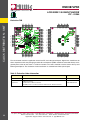
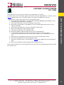
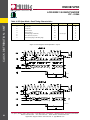
Analog Devices Welcomes
Hittite Microwave Corporation
NO CONTENT ON THE ATTACHED DOCUMENT HAS CHANGED
www.analog.com
www.hittite.com
THIS PAGE INTENTIONALLY LEFT BLANK
HMC987LP5E
v03.1112
Clock Distribution - SMT
LOW NOISE 1:9 FANOUT BUFFER
DC - 8 GHz
Typical Applications
Features
The is suitable for:
Ultra Low Noise Floor: -166 dBc/Hz @ 2 GHz
• SONET, Fibre Channel, GigE Clock Distribution
• ADC/DAC Clock Distribution
• Low Skew and Jitter Clock or Data Fanout
• Wireless/Wired Communications
• Level Translation
• High Performance Instrumentation
• Medical Imaging
• Single-Ended to Differential Conversion
Wideband: DC - 8 GHz Operating Frequency
Flexible Input Interface:
LVPECL, LVDS, CML, CMOS Compatible
AC or DC Coupling
On-Chip Termination 50 or 150 Ω (100/300 Ω Diff.)
Multiple Output Drivers:
Up to 8 Differential or 16 Single-Ended LVPECL
Outputs:
800 mVpp into 50 Ω Single-Ended (+3 dBm Fo)
One Adjustable Power CML/RF Output:
-9 to 3 dBm Single-Ended
Serial or Parallel Control, Hardware Chip-Enable
Power-Down Current < 1 uA
32 Lead 5x5 mm SMT Package 25 mm2
Functional Diagram
General Description
The 1-to-9 fanout buffer is designed for low noise clock
distribution. It is intended to generate relatively square
wave outputs with rise/fall times < 100 ps. The low skew
and jitter outputs of the HMC987LP5E, combined with
its fast rise/fall times, leads to controllable low-noise
switching of downstream circuits such as mixers,
ADCs/DACs or SERDES devices. The noise floor
is particularly important in these applications, when
the clock-network bandwidth is wide enough to allow
square-wave switching. Driven at 2 GHz, outputs of
the HMC987LP5E have a noise floor of -166 dBc/Hz,
corresponding to a jitter density of 0.6 asec/rtHz - or
50 fs over an 8 GHz bandwidth.
The input stage can be driven single-ended or
differentially, in a variety of signal formats (CML,
LVDS, LVPECL or CMOS), AC or DC coupled. The
input stage also features adjustable input impedance.
It has 8 LVPECL outputs, and 1 CML output with
adjustable swing/power-level in 3 dB steps.
Individual output stages may be enabled or disabled
for power-savings when not required using either
hardware control pins, or under control of a serial-port
interface.
1
For price, delivery and to place orders: Hittite Microwave Corporation, 2 Elizabeth Drive, Chelmsford, MA 01824
Phone: 978-250-3343
Fax: 978-250-3373
Order On-line at www.hittite.com
Application Support: Phone: 978-250-3343 or [email protected]
HMC987LP5E
v03.1112
LOW NOISE 1:9 FANOUT BUFFER
DC - 8 GHz
Clock Distribution - SMT
Table 1. Electrical Specifications
Unless otherwise specified: T = 27 °C, Regulated VDD of 3.3 V, 2 GHz, 6 dBm in, AC coupled single ended input and
output, 120 Ω/leg DC termination, AC coupled into 50 Ω measuring load. Effects of customer eval board (“Evaluation
PCB Schematic”) are de-embedded. For convenience, all voltages are referenced to GND (0V), but negative supply
references are acceptable.
Parameter
Conditions
Min.
Typ.
Max.
Units
VDD (VCCHF=VCCA=VCCB=VCCRF)
3.0
3.3
3.6
V
Input Common Mode Voltage
1.35
2
VDD - 0.2
V
Input Swing (Single Ended)
0.2
2
Vpp
DC Input Characteristics
Input Capacitance
0.5
pF
Input Impedance
Single-Ended
Selectable
50 / 150
Ω
Differential
Selectable
100 / 300
Ω
165
µA
Input Bias Current
Base current under external
DC bias, Internal termination
open.
Logic Inputs
Switching Threshold (Vsw)
VIH/VIL within 50 mV of Vsw
38
47
54
%VDD
VDD - 1.2
VDD - 1.0
VDD - 0.8
V
LVPECL DC Output Characteristics
Output Voltage High Level
@ 3.3 V = 2.25
Ouput Voltage Common Mode
@ 3.3 V = 1.82
VDD - 1.7
VDD - 1.5
VDD - 1.3
V
Output Voltage Low Level
@ 3.3 V = 1.42
VDD - 2.1
VDD - 1.9
VDD - 1.7
V
Output Voltage, Single-Ended
800
mVpp
AC Performance
Input/Output Frequency [1]
> 400 Vpp single-ended
DC
3 dB Bandwidth
Output Rise/Fall Time
20% to 80%
Typical Channel Skew
Across all LVPECL outputs
relative to channel 1
0
8000
MHz
4000
MHz
65
ps
1.5
3.1
ps
Small Signal Gain S21
1000 MHz
26
dB
4000 MHz
15
dB
1000 MHz
-20
dBm
4000 MHz
-10
dBm
1000 MHz
2.5
dBm
4000 MHz
-0.5
dBm
Input P1dB
Saturated Power in fundamental tone (Single-Ended)
Output Voltage Swing (Vppd into 100 Ω)
700 MHz
1.5
1.6
1.7
V
2000 MHz
1.2
1.3
1.4
V
[1] For frequencies < 700 MHz, square wave signals should be used to maintain high quality phase noise performance.
2
For price, delivery and to place orders: Hittite Microwave Corporation, 2 Elizabeth Drive, Chelmsford, MA 01824
Phone: 978-250-3343
Fax: 978-250-3373
Order On-line at www.hittite.com
Application Support: Phone: 978-250-3343 or [email protected]
HMC987LP5E
v03.1112
LOW NOISE 1:9 FANOUT BUFFER
DC - 8 GHz
Parameter
Conditions
4000 MHz
Min.
Typ.
Max.
Units
1.1
1.2
1.3
V
Harmonics
Fo
2
dBm
2Fo
-25
dBc
3Fo
-8
dBc
4Fo
-28
dBc
5Fo
-12
dBc
SSB Phase Noise at 100 Hz Offset
622.08 MHz Carrier Frequency
-147
dBc/Hz
1750 MHz Carrier Frequency
-147
dBc/Hz
4000 MHz Carrier Frequency
-147
dBc/Hz
SSB Phase Noise Floor [2]
100 MHz Carrier Frequency
-167
dBc/Hz
622.08 MHz Carrier Frequency
-167
dBc/Hz
1750 MHz Carrier Frequency
-166
dBc/Hz
2000 MHz Carrier Frequency
-166
dBc/Hz
4000 MHz Carrier Frequency
-163
dBc/Hz
4200 MHz Carrier Frequency
-162
dBc/Hz
1.8
asec/√Hz
1750 MHz Carrier Frequency
0.7
asec/√Hz
4000 MHz Carrier Frequency
0.5
asec/√Hz
17
fs rms
12 kHz to 20 MHz
8
fs rms
20 kHz to 80 MHz
17
fs rms
50 kHz to 80 MHz
17
fs rms
4 MHz to 80 MHz
16
fs rms
100 Hz to 100 MHz
7
fs rms
12 kHz to 20 MHz
3
fs rms
20 kHz to 80 MHz
6
fs rms
50 kHz to 80 MHz
6
fs rms
Clock Distribution - SMT
Table 1. Electrical Specifications (Continued...)
Floor Jitter Density
622.08 MHz Carrier Frequency
Integrated RMS Jitter
100 Hz to 100 MHz
622.08 MHz Carrier Frequency
1750 MHz Carrier Frequency
4000 MHz Carrier Frequency
Output Return Loss
4 MHz to 80 MHz
6
fs rms
100 Hz to 100 MHz
4
fs rms
12 kHz to 20 MHz
2
fs rms
20 kHz to 80 MHz
4
fs rms
50 kHz to 80 MHz
4
fs rms
4 MHz to 80 MHz
4
fs rms
500 MHz to 4 GHz
-16
-12
-8
dB
[2] CML buffer has similar phase noise characteristics at maximum output power level.
For price, delivery and to place orders: Hittite Microwave Corporation, 2 Elizabeth Drive, Chelmsford, MA 01824
Phone: 978-250-3343
Fax: 978-250-3373
Order On-line at www.hittite.com
Application Support: Phone: 978-250-3343 or [email protected]
3
HMC987LP5E
v03.1112
LOW NOISE 1:9 FANOUT BUFFER
DC - 8 GHz
Table 1. Electrical Specifications (Continued...)
Clock Distribution - SMT
Parameter
Conditions
Min.
Typ.
Max.
Units
Isolation
In to Out - Chip Disabled
47
dB
Off isolation - Relative to Power of neighboring driven port
700 MHz
60
48
dB
4000 MHz
50
32
dB
Output to Output Isolation with 500 MHz Aggressor Signal Injected into Output Port
To Locally paired output buffer
25
dB
To other buffers
45
dB
5000
MHz
RF Output Buffer
3 dB Bandwidth
Max Output Power (vs Temperature at
2 GHz)
Single-Ended
3
Power Control Range (3 dB steps)
Single-Ended
-9
Delay Relative to LVPECL Output
3.2
dBm
3
dBm
-140
ps
0.8
ps/V
7
dB
Power Supply Rejection
FM/Phase Pushing
AM Rejection
Current Consumption (3.3 V Unloaded Outputs)
Chip Disabled
1
µA
1 Output
60
mA
2 Outputs
71
mA
3 Outputs
97
mA
4 Outputs
108
mA
5 Outputs
134
mA
6 Outputs
144
mA
7 Outputs
170
mA
8 Outputs
8 + RF Buffer (Min to Max Power)
180
198
mA
234
mA
1.1
V
SPI Interface
Vil
Vih
2.0
Vol
Voh
4
V
0.4
2.3
V
V
For price, delivery and to place orders: Hittite Microwave Corporation, 2 Elizabeth Drive, Chelmsford, MA 01824
Phone: 978-250-3343
Fax: 978-250-3373
Order On-line at www.hittite.com
Application Support: Phone: 978-250-3343 or [email protected]
HMC987LP5E
v03.1112
LOW NOISE 1:9 FANOUT BUFFER
DC - 8 GHz
TYPICAL PERFORMANCE CHARACTERISTICS
Figure 1. LVPECL Output vs. Frequency [1]
Figure 2. LVPECL Output vs. Frequency [1]
0.4
4 GHz OUTP
0.6
2 GHz OUTP
4 GHz OUTN
0.3
AMPLITUDE (V differential)
OUTPUT VOLTAGE (V)
0.4
0.2
0.1
0
-0.1
-0.2
-0.3
0.2
0
-0.2
4 GHz
2 GHz
1 GHz
-0.4
-0.6
2 GHz OUTN
-0.4
-800
-600
-400
1 GHz OUTP
-200
0
200
1 GHz OUTN
400
600
-0.8
800
0
TIME (picoseconds)
20
40
60
80
100
120
TIME (ps)
Figure 3. Current Consumption vs. Num.
of Enabled Buffers & Load Resistors[2]
Figure 4. Skew of LVPECL Outputs
Relative to Output Channel 1 [4]
500
15
120 Ohm DC Termination
CURRENT (mA)
200 Ohm DC Termination
300
300 Ohm DC Termination
200
RELATIVE DELAY (psec)
10
400
100
5
Clock Distribution - SMT
Unless otherwise specified: T = 27 °C, Regulated VDD = 3.3 V, 2 GHz, 6 dBm in, AC coupled single ended input and output, 120 Ω/leg DC termination,
AC coupled into 50 Ω measuring load.
0
-5
-10
Ground Current (Does not depend on termination)
-15
0
1
2
3
4
5
5
6
7
8
P1
RF Min RF Max
Figure 5. Fundamental Output Power vs.
Input Power [3]
OUTPUT TRACE LOSS (dB)
OUTPUT POWER (dBm)
P6
P7
P8
-1
400 MHz
3 GHz
4 GHz
5 GHz
-15
-2
-3
-4
-5
-6
6 GHz
-20
-30
P5
0
2 GHz
-10
P4
Figure 6. Evaluation Board LVPECL Output
Trace Loss vs. Frequency [5]
5
-5
P3
OUTPUT CHANNEL
NUMBER OF OUTPUTS SUCCESSIVELY TURNED ON
0
P2
-7
-24
-18
-12
-6
INPUT POWER (dBm)
0
6
100
1000
OUTPUT FREQUENCY (MHz)
10000
[1] +2dBm input, Uncorrected for board loss. Measurement is band limited by the trace bandwidth of 7 GHz.
[2] Buffers 1 through 8 are successively turned on. RF Min - RF buffer turned on with minimum gain, RF Max - RF buffer turned on with maximum gain
[3] 200 Ω Termination, Corrected for board loss.
[4] Characterized at 2 GHz, Effects of customer evaluation board skew and loss are embedded.
[5] The graph shows only output trace distortion.
For price, delivery and to place orders: Hittite Microwave Corporation, 2 Elizabeth Drive, Chelmsford, MA 01824
Phone: 978-250-3343
Fax: 978-250-3373
Order On-line at www.hittite.com
Application Support: Phone: 978-250-3343 or [email protected]
5
HMC987LP5E
v03.1112
LOW NOISE 1:9 FANOUT BUFFER
DC - 8 GHz
6
3
3
Reg04h[2:0]= 5d
OUTPUT POWER (dBm)
OUTPUT POWER (dBm)
Figure 8. RF Output Power Control
4
2
1
0
-1
Reg04h[2:0] = 4d
0
Reg04h[2:0] = 3d
-3
Reg04h[2:0] = 2d
-6
Reg04h[2:0] = 1d
-9
-40 C
27 C
85 C
-2
-12
-3
100
1000
FREQUENCY (MHz)
100
10000
Figure 9. Fundamental Output Power vs.
Frequency & Temperature [6]
4
4
3
3
2
1
0
-1
-40 C
27 C
85 C
1000
FREQUENCY (MHz)
10000
Figure 10. Fundamental Output Power vs.
Frequency & Supply Voltage at 27 °C [6]
OUTPUT POWER (dBm)
OUTPUT POWER (dBm)
Clock Distribution - SMT
Figure 7. RF Buffer Fo Output Power vs.
Frequency & Temperature (Max Gain)
2
1
3.6 V
0
3.5 V
3.3 V
-1
-2
-2
-3
-3
3.2 V
3.0 V
100
1000
OUTPUT FREQUENCY (MHz)
100
10000
Figure 11. Fundamental Output Power vs.
Frequency & Termination at 27 °C [6]
1000
OUTPUT FREQUENCY (MHz)
10000
Figure 12. Signal Swing vs. Frequency [7]
1.6
3
1.4
1.2
SIGNAL SWING (Vppd)
OUTPUT POWER (dBm)
2
1
0
-1
-2
120 Ohms
200 Ohms
300 Ohms
0.8
Observed and Not Corrected
For Evaluation Board Loss
0.6
0.4
0.2
0
-3
100
Corrected For Evaluation Board Loss
1
1000
OUTPUT FREQUENCY (MHz)
10000
0
1000
2000
3000
4000
5000
FREQUENCY (MHz)
6000
7000
8000
[6] Measured single-ended. Corrected for trace loss. 200 Ω DC termination, 3.3 V +6 dBm single-ended input. HMC987LP5E AC coupled to 50 Ω
instrument.
[7] Input signal power = + 6 dBm. 120 Ω/leg DC termination. AC coupled via 50 pF to 26 GHz Oscilloscope (50 Ohm/leg termination).
6
For price, delivery and to place orders: Hittite Microwave Corporation, 2 Elizabeth Drive, Chelmsford, MA 01824
Phone: 978-250-3343
Fax: 978-250-3373
Order On-line at www.hittite.com
Application Support: Phone: 978-250-3343 or [email protected]
HMC987LP5E
v03.1112
LOW NOISE 1:9 FANOUT BUFFER
DC - 8 GHz
Figure 13. Phase Noise Performance
at 2 GHz (Differential Drive) [9]
Figure 14. Phase Noise Floor vs. Slew Rate
-110
-162
-120
-130
4 GHz
-163
PHASE NOI SE (dBc/Hz)
PHASE NOISE (dBc/Hz)
Pin = -3 dBm
Source + Fanout Output Noise
-140
-150
-160
-170
-164
Pin = 0 dBm
Pin = 3 dBm
-166
100 MHz
2 GHz
-167
Pin = 10 dBm
-168
HMC830LP6GE Used as Source
-180
Pin = 10 dBm
-169
10
3
10
4
5
6
10
10
FREQUENCY OFFSET (Hz)
10
7
10
8
0
2
4
6
8
10
12
SLEW RATE (V/nsec)
Figure 15. Phase Noise Floor
at 1.6 GHz vs. Input Power
Figure 16. Phase Noise Performance with
Low Frequency Sinusoidal Inputs [8]
-156
-248
-158
-250
-160
-252
FOM (dBc/Hz)
PHASE NOISE (dBc/Hz)
Pin = 0 dBm
-165
-162
-254
-164
-256
-166
-258
Clock Distribution - SMT
-161
-260
-168
-15
-10
-5
0
INPUT POWER (dBm)
5
0
10
Figure 17. Phase Noise Floor
at 2 GHz vs. VDD and DC Termination
500
1000
1500
SINUSOIDAL INPUT FREQUENCY (MHz)
2000
Figure 18. Phase Noise Floor vs.
Temperature
-160
-162
200 Ohm Termination
120 Ohm Termination
-166
300 Ohm Termination
-168
PHASE NOISE (dBc/Hz)
PHASE NOISE (dBc/Hz)
-162
-164
Frequency = 4.2 GHz
-164
Frequency = 2 GHz
-166
-168
Frequency = 100 MHz
-170
-170
2.7
2.8
2.9
3
3.1
VDD
3.2
3.3
3.4
3.5
-50
0
50
100
TEMPERATURE (Deg. C)
[8] Input power = 10 dBm single-ended. Phase Noise Floor (dBc/Hz) = FOM (dBc/Hz)) + 10log(Fout [Hz])
[9] HMC830LP6GE used as signal source, Driving +9 dBm differentially.
For price, delivery and to place orders: Hittite Microwave Corporation, 2 Elizabeth Drive, Chelmsford, MA 01824
Phone: 978-250-3343
Fax: 978-250-3373
Order On-line at www.hittite.com
Application Support: Phone: 978-250-3343 or [email protected]
7
HMC987LP5E
v03.1112
LOW NOISE 1:9 FANOUT BUFFER
DC - 8 GHz
Figure 19. Harmonic Performance
(Single-Ended Input & Output) [10]
Figure 20. S-Parameters - S11 [11]
0
0
Fo
-5
Differential
-10
-20
S11 (dB)
POWER (dBm)
-10
2Fo
-30
3f0
3Fo
-40
-15
Single-Ended
-20
-50
4Fo
-60
5Fo
-25
-70
-30
100
1000
10000
0
2000
FREQUENCY (MHz)
Figure 21. S-Parameters - S12 [11]
4000
6000
FREQUENCY (MHz)
8000
10000
Figure 22. S-Parameters - S22 [11]
0
-30
-40
-5
Single-Ended
-50
-10
Single-Ended
S22 (dB)
-60
S12 (dB)
Clock Distribution - SMT
10
-70
-80
-15
Differential
-20
-90
Differential
-25
-100
-30
-110
0
2000
4000
6000
FREQUENCY (MHz)
8000
10000
0
2000
4000
6000
8000
10000
FREQUENCY (MHz)
[10] Not corrected for board/cable loss.
[11] Effects of the customer evaluation board are not corrected. Improvements in S11 and S22 are possible under different evaluation board
configurations
8
For price, delivery and to place orders: Hittite Microwave Corporation, 2 Elizabeth Drive, Chelmsford, MA 01824
Phone: 978-250-3343
Fax: 978-250-3373
Order On-line at www.hittite.com
Application Support: Phone: 978-250-3343 or [email protected]
HMC987LP5E
v03.1112
LOW NOISE 1:9 FANOUT BUFFER
DC - 8 GHz
Table 2. Pin Descriptions
Function
Description
1
VCCHF
2
CLKP
3
CLKN
4
SDI
Serial port data input
5
SDO
Serial port data output
6
PMODE-SEL
7
RFOUTP
8
RFOUTN
9
VCCRF
10
SCLK
Serial port clock
11
SEN
Serial port latch enable
12
OUTP8
13
OUTN8
14
OUTP7
15
OUTN7
16
VCCB
17
OUTN6
18
OUTP6
19
OUTN5
20
OUTP5
21
OUTP4
22
OUTN4
23
OUTP3
24
OUTN3
25
VCCA
26
OUTN2
27
OUTP2
28
OUTN1
29
OUTP1
30
RFBUFEN
31
CEN
32
NC
Power Supply
Differential clock inputs
Parallel mode select. If 1, pins (SCLK, SDI, SEN) are interpreted as a control-word which enables
different buffers. See section “Parallel Port Control”
Differential signal output
Power supply
Differential signal output
Differential signal output
Clock Distribution - SMT
Pin Number
Power supply
Differential signal output
Differential signal output
Differential signal output
Differential signal output
Power supply
Differential signal output
Differential signal output
Active high RF buffer enable. The polarity of this control input can be swapped via SPI bit
Reg03h[4].
Hardware chip enable. Logic 0=Power Down, Logic 1=Active
No Connect
For price, delivery and to place orders: Hittite Microwave Corporation, 2 Elizabeth Drive, Chelmsford, MA 01824
Phone: 978-250-3343
Fax: 978-250-3373
Order On-line at www.hittite.com
Application Support: Phone: 978-250-3343 or [email protected]
9
HMC987LP5E
v03.1112
LOW NOISE 1:9 FANOUT BUFFER
DC - 8 GHz
Table 3. Absolute Maximum Ratings
Clock Distribution - SMT
Parameter
10
Max Vdc to paddle on supply pins 1, 9, 16, 25
Rating
-0.3 V to +4 V
Max RF Power CLKP, CLKN
15 dBm single-ended
CLKP, CLKN
- 0.3 V to 3.6 V
LVPECL Min Output Load Resistor
100 Ohms to GND
LVPECL Output Load Current
40 mA/leg
Digital Load
1 kΩ min
Digital Input Voltage Range
-0.3 to 3.6 V
Thermal Resistance (junction to ground paddle)
25 0C/W
Operating Temperature Range
-40 OC to +85 OC
Storage Temperature Range
-65 OC to + 125 OC
Maximum Junction Temperature
+125 OC
Reflow Soldering
Peak Temperature
260 OC
Time at Peak Temperature
40 sec
ESD Sensitivity HBM
Class 1B
Stresses above those listed under Absolute Maximum Ratings may cause permanent damage to the device. This is
a stress rating only; functional operation of the device at these or any other conditions above those indicated in the
operational section of this specification is not implied. Exposure to absolute maximum rating conditions for extended
periods may affect device reliability.
For price, delivery and to place orders: Hittite Microwave Corporation, 2 Elizabeth Drive, Chelmsford, MA 01824
Phone: 978-250-3343
Fax: 978-250-3373
Order On-line at www.hittite.com
Application Support: Phone: 978-250-3343 or [email protected]
HMC987LP5E
v03.1112
LOW NOISE 1:9 FANOUT BUFFER
DC - 8 GHz
Clock Distribution - SMT
Outline Drawing
NOTES:
[1] PACKAGE BODY MATERIAL: LOW STRESS INJECTION MOLDED PLASTIC SILICA AND SILICON IMPREGNATED.
[2] LEAD AND GROUND PADDLE MATERIAL: COPPER ALLOY.
[3] LEAD AND GROUND PADDLE PLATING: 100% MATTE TIN.
[4] DIMENSIONS ARE IN INCHES [MILLIMETERS].
[5] LEAD SPACING TOLERANCE IS NON-CUMULATIVE.
[6] PAD BURR LENGTH SHALL BE 0.15 mm MAX. PAD BURR HEIGHT SHALL BE 0.05 mm MAX.
[7] PACKAGE WARP SHALL NOT EXCEED 0.05 mm
[8] ALL GROUND LEADS AND GROUND PADDLE MUST BE SOLDERED TO PCB RF GROUND.
[9] REFER TO HITTITE APPLICATION NOTE FOR SUGGESTED PCB LAND PATTERN.
Table 4. Package Information
Part Number
Package Body Material
Lead Finish
MSL Rating
Package Marking [1]
RoHS-compliant Low Stress Injection Molded Plastic
100% matte Sn
MSL1[2]
H987
XXXX
[1] 4-Digit lot number XXXX
[2] Max peak reflow temperature of 260°C
For price, delivery and to place orders: Hittite Microwave Corporation, 2 Elizabeth Drive, Chelmsford, MA 01824
Phone: 978-250-3343
Fax: 978-250-3373
Order On-line at www.hittite.com
Application Support: Phone: 978-250-3343 or [email protected]
11
HMC987LP5E
v03.1112
LOW NOISE 1:9 FANOUT BUFFER
DC - 8 GHz
Clock Distribution - SMT
Evaluation PCB
The circuit board used in the application should use RF circuit design techniques. Signal lines should have 50
Ohms impedance while the package ground leads and exposed paddle should be connected directly to the
ground plane similar to that shown. A sufficient number of via holes should be used to connect the top and
bottom ground planes. The evaluation circuit board shown is available from Hittite upon request.
Table 5. Evaluation Order Information
12
Item
Contents
Part Number
Evaluation PCB
Evaluation PCB
EVAL01-HMC987LP5E
Evaluation Kit
Evaluation PCB
USB Interface Board
6’ USB A Male to USB B Female Cable
CD ROM (Contains User Manual, Evaluation PCB Schematic, Evaluation Software,
EKIT01-HMC987LP5E
For price, delivery and to place orders: Hittite Microwave Corporation, 2 Elizabeth Drive, Chelmsford, MA 01824
Phone: 978-250-3343
Fax: 978-250-3373
Order On-line at www.hittite.com
Application Support: Phone: 978-250-3343 or [email protected]
A
B
C
NC
NC
NC
NC
0
R4
GND
9
11
6
OUT7-N
OUT7-P
OUT8-N
OUT8-P
RFOUT-N
RFOUT-P
CLK-N
CLK-P
J21
J19
J17
J14
J4
J3
J2
J1
HEADER TOUSB BOARD
SSW-106-01-T-D
7
8
5
6
12
3
1
4
2
J30
10
0
R1
0.1uF
1K
R35
DEPOP
DEPOP
J12
200K
R5
R31
J5
R63
DEPOP
R61
0.1uF
C1
R34
DEPOP
R33
DEPOP
DEPOP
100pF
C59
100pF
C47
100pF
C37
100pF
C27
R32
J6
0
R12
0
R11
200K
R6
4.7uF
C6
82K
R3
R36
DEPOP
SCK
SDI
SDO
SEN
CEN
4.7uF
C3
1
2
D
C4
1
2
5
0
BAND
GAP
200K
R9
100pF
C15
100pF
C14
C57
100pF
DEPOP
C56
DEPOP
DEPOP
C44
C58
100pF
C45
100pF
DEPOP
DEPOP
C46
DEPOP
C34
C24
100pF
C12
100pF
C10
J11
200K
R10
C36
C35
400
DEPOP
100pF
C25
DEPOP
C9
DEPOP
C8
J10
VRX
REF
RD
EN
15
DEPOP
C26
R14
0
R13
J8
200K
R8
4.7uF
C2
4
3
2
1
14
NC
13
NC
16
5
TP2
1
2
NC
HV
6
1
2
NC
VDD
NC
7
NC
8
NC
NC
NC
VR
NC
U1
9
10
11
12
DEPOP
C11
200
200
R48
200
R45
200
R42
J7
200K
R7
R39
DEPOP
C13
J9
HMC976LP3E
1
2
TP1
1
2
+5V
MAX
0
R62
DEPOP
C113
0
R46
DEPOP
C114
0
R40
DEPOP
DEPOP
4
DEPOP
DEPOP
C105
C104
C7
0.1uF
VCCRF
C103
C106
PMOD_SEL
RFBUF_EN
200K
R2
VCCRF
1
2
4
DEPOP
C55
DEPOP
C43
DEPOP
C33
DEPOP
C23
VCCRF
VCCA
8
7
6
5
4
3
0.1uF
C22
1
2
100pF
C5
0
R22
0
R18
0
R19
0
R20
RFOUTN
RFOUTP
PMODE_SEL
SDO
SDI
CLKN
CLKP
VCCB
VCCHF
VCCHF
100pF
C101
VCCHF
NC
32
3.3V 350mA
0.1uF
C21
30
5
29
SPI
RFBUFEN
31
NC
VCCRF
9
CEN
10
SCLK
11
SEN
12
27
28
OUTP1
OUTP8
26
OUTN1
OUTN8
13
OUTP2
25
VCCA
OUTN2
OUTN7
For price, delivery and to place orders: Hittite Microwave Corporation, 2 Elizabeth Drive, Chelmsford, MA 01824
Phone: 978-250-3343
Fax: 978-250-3373
Order On-line at www.hittite.com
Application Support: Phone: 978-250-3343 or [email protected]
3
24
17
18
19
20
21
22
23
100pF
C102
VCCB
HMC987LP5E
OUTN6
OUTP6
OUTN5
OUTP5
OUTP4
OUTN4
OUTP3
OUTN3
U2
100pF
0.1uF
C54
0.1uF
C53
B
C100
CP110885
A
VCCA
ECN#
CP110719
REV
0
R30
0
R29
0
R24
0
R23
0
R21
0
R15
0
R16
0
R17
----
----PRODUCTION RELEASE CP110719
0
R26
0
R25
0
R28
0
DESCRIPTION
REVISIONS
DEPOP
C61
DEPOP
C65
DEPOP
C64
DEPOP
C60
DEPOP
C52
DEPOP
C42
DEPOP
C32
DEPOP
C20
DEPOP
C74
DEPOP
C73
DEPOP
C72
DEPOP
C71
2
DEPOP
C109
0
R55
DEPOP
C107
0
R43
DEPOP
C108
0
R37
J16
DRAWN BY
DRAWING#:
PROJECT
TITLE
DEPOP
C112
0
R58
DEPOP
C111
0
R60
DEPOP
C110
0
R59
200
R51
200
R49
200
R47
200
R44
200
200
R41
R38
DEPOP
C66
DEPOP
C75
DEPOP
C84
DEPOP
C83
DEPOP
C82
DEPOP
C80
100pF
C79
100pF
C62
100pF
C50
100pF
C40
100pF
C30
100pF
100pF
C67
100pF
C86
100pF
C85
100pF
C94
100pF
C92
100pF
C81
DEPOP
C78
DEPOP
C68
DEPOP
C49
DEPOP
C39
DEPOP
C29
DEPOP
C17
DEPOP
C76
DEPOP
C87
DEPOP
C95
DEPOP
C93
DEPOP
C91
DEPOP
C90
D.YOUNG
130-00080-00
HMC987LP5E
DATE
11/18/2010
1
1
DATE
06/23/11
05/25/11
1
REV
OUT6-N
OUT6-P
OUT5-N
OUT5-P
OUT4-P
OUT4-N
OUT3-P
OUT3-N
OUT2-N
OUT2-P
OUT1-N
OUT1-P
C
OF
SIZE
J29
J28
J27
J26
J25
J24
J23
J22
J20
J18
J15
J13
29-06-2011_13:34
1CN88
CODE ID NO.
SHEET
SCH, EVAL CUSTOMER
20 Alpha Rd Chelmsford, MA 01824
100pF
C77
100pF
C97
100pF
C96
100pF
C99
100pF
C98
100pF
C89
100pF
C88
100pF
C69
100pF
C48
100pF
C38
100pF
C28
100pF
C16
D. ACEVAL
V.VADUVA
NAME
1
HITTITE MICROWAVE CORPORATION
200
R50
200
R54
200
R53
200
R57
200
R56
200
R52
DEPOP
C70
DEPOP
C63
DEPOP
C51
DEPOP
C41
DEPOP
C31
DEPOP
C19
C18
CHANGER32,R35,R36,R63,R38,R39,R41,R42,R44,R45,R47,R48,R49,R50,R51,R52,R53,R54,R56,R57CP110885
R27
ZONE
2
B
Clock Distribution - SMT
3
16
OUTP7
14
VCCB
15
6
A
B
C
D
v03.1112
HMC987LP5E
LOW NOISE 1:9 FANOUT BUFFER
DC - 8 GHz
Evaluation PCB Schematic
13
NOTICE OF PROPRIETARY PROPERTY: THIS DOCUMENT AND THE INFORMATION CONTAINED IN IT ARE THE PROPRIETARY PROPERTY OF HITTITE MICROWAVE CORPORATION. IT MAY NOT BE COPIED OR USED
IN ANY MANNER NOR MAY ANY OF THE INFORMATION IN OR UPON IT BE USED FOR ANY PURPOSE WITHOUT THE EXPRESSED WRITTEN CONSENT OF AN AUTHORIZED AGENT OF HITTITE MICROWAVE CORPORATION.
HMC987LP5E
v03.1112
LOW NOISE 1:9 FANOUT BUFFER
DC - 8 GHz
Clock Distribution - SMT
Theory of Operation
Parallel Port Control
The various outputs of the can be enabled/disabled by using parallel pin control, or via the SPI. In parallel-mode
(PMODE-SEL = 1), the SPI input pins (SCLK, SKI, SEN) are re-interpreted as a 3-bit control bus, and enable the
LVPECL drivers according to the following truth table.
SCLK, SDI, SEN
000: OUT2
001: OUT2 + OUT7
010: OUT2 + OUT7 + OUT4
011: OUT2 + OUT7 + OUT4 + OUT6
100: OUT2 + OUT7 + OUT4 + OUT6 + OUT5
101: OUT2 + OUT7 + OUT4 + OUT6 + OUT5 + OUT3
110: OUT2 + OUT7 + OUT4 + OUT6 + OUT5 + OUT3 + OUT8
111: OUT2 + OUT7 + OUT4 + OUT6 + OUT5 + OUT3 + OUT8 + OUT1
Under SPI control (PMODE-SEL = 0, see section “Register Map” for the register map and SPI protocol details), there
is slightly more flexibility in that any combination of buffers can be enabled or disabled via the individual buffer enable
bits in Reg02h.
The part features switches on both the input and output signals, so that when the part is disabled (via either the
CEN pin, or the SPI control bit Reg01h[0]), the power-down current drops to < 2 µA, regardless of the IO termination
scheme.
Input Stage
The input stage, Figure 26, is flexible. It can be driven single-ended or differential, with LVPECL, LVDS, or CML
signals. If driven single-ended, a large AC coupling cap to ground should be used on the undriven input. The input
impedance is selectable, via Reg03h[3], between 50 Ω or 150 Ω single ended(100 Ω or 300 Ω differential). The DC
bias level of 2.0 V can be generated internally by programming Reg03[1]=1 (default configuration), supplied externally,
or generated via an LVPECL termination network inside the part.
Chip Enable
The HMC987 has a chip enable feature, CEN, which can be used to power down or deactivate the LVPECL and RF
outputs. This can be done by either hardware, pin 31, or a SPI command, Reg01.
For a hardware selection, a logic 0 applied to CEN will power down the HMC987, however, SPI commands can
still be written which will be recognized upon when a logic 1 is applied to CEN. Note, there is no internal pull-up or
pull-down and this pin must be terminated. To control CEN by SPI command, Reg 01h[0] is set to 1, which is the default
mode, and enables the outputs. When Reg01[0]=0 then the outputs are disabled. Either a hardware, pin 31, or a SPI
command will disable the outputs.
14
For price, delivery and to place orders: Hittite Microwave Corporation, 2 Elizabeth Drive, Chelmsford, MA 01824
Phone: 978-250-3343
Fax: 978-250-3373
Order On-line at www.hittite.com
Application Support: Phone: 978-250-3343 or [email protected]
HMC987LP5E
v03.1112
Reg03h[3]=1
Closed
(Default State)
Reg03h[1]=1
Closed
(Default State)
Termination Select
Reg03h[2]=0
Open
(Default State)
Figure 26. Input Stage
Clock Distribution - SMT
LOW NOISE 1:9 FANOUT BUFFER
DC - 8 GHz
Figures 27 to Figure 31 illustrate common input interface configurations.
Figure 27. DC Coupled CML Interface
Figure 28. DC Coupled CMOS Interface
For price, delivery and to place orders: Hittite Microwave Corporation, 2 Elizabeth Drive, Chelmsford, MA 01824
Phone: 978-250-3343
Fax: 978-250-3373
Order On-line at www.hittite.com
Application Support: Phone: 978-250-3343 or [email protected]
15
HMC987LP5E
v03.1112
Clock Distribution - SMT
LOW NOISE 1:9 FANOUT BUFFER
DC - 8 GHz
Figure 29. DC Coupled LVPECL Interface
Figure 30. AC Coupled Differential CML / LVPECL /
LVDS / CMOS Interface
Figure 31. AC Coupled Single-Ended CML / LVPECL
/ LVDS / CMOS Interface
LVPECL Output Stage
The LVPECL output driver produces up to 1.6 Vppd swing into 100 Ω differencial loads. LVPECL drivers are terminated
with off-chip resistors that provide the DC current through the emitter-follower output stage. The output stage has
a switch which disconnects the output driver from the load when not used. The switch series resistor significantly
improves the output match when driving into 50 Ω transmission lines. The switch series resistor causes a small DC
level shift and swing degradation, depending on the termination current.
If unused, disabled LVPECL outputs can be left floating, terminated, or grounded.
16
For price, delivery and to place orders: Hittite Microwave Corporation, 2 Elizabeth Drive, Chelmsford, MA 01824
Phone: 978-250-3343
Fax: 978-250-3373
Order On-line at www.hittite.com
Application Support: Phone: 978-250-3343 or [email protected]
HMC987LP5E
v03.1112
Figure 32. Output Stage
Figures 34 35 36 illustrate common output interface configurations.
Figure 33. DC Coupled to LVPECL Interface
Clock Distribution - SMT
LOW NOISE 1:9 FANOUT BUFFER
DC - 8 GHz
Figure 34. AC coupled to LVDS / CML / LVPECL /
CMOS
For price, delivery and to place orders: Hittite Microwave Corporation, 2 Elizabeth Drive, Chelmsford, MA 01824
Phone: 978-250-3343
Fax: 978-250-3373
Order On-line at www.hittite.com
Application Support: Phone: 978-250-3343 or [email protected]
17
HMC987LP5E
v03.1112
Clock Distribution - SMT
LOW NOISE 1:9 FANOUT BUFFER
DC - 8 GHz
Figure 35. DC Coupled to CMOS Interface
The user has a number of choices in how they connect LVPECL drivers and receivers, and there are great number
of resources that deal in detail with this issue. As a quick introduction, there are compromises between matching
performance, common mode levels, and signal swing. For clocking applications, the user often has the luxury of
using AC coupling, unlike in many data-path situations. Figure 36 shows a simplified interface schematic between an
LVPECL output and input stage - where various options and trade-offs for the termination components are provided
in Table 6. The Hittite evaluation board has a great deal of flexibility in how the I/Os are configured, and allows the
configuration in Figure 34, among many others.
Figure 36. Recommended Interface Diagram
Table 6. Interface Values
Rs - Used to increase Ro to match to 50 Ω environment. already has ~ 10 Ω internally.
0Ω
Hittite EVB: Largest signal swing, lowest common mode shift
10 Ω
Better S22
RL - DC current termination for LVPECL output stage
120 Ω
Hittite EVB default: Standard LVPECL termination voltages
200 Ω
Reduced current, no performance degradation
300 Ω
Further reduced current, lower output power but flatter frequency response
OPEN
If using internal DC termination network at the Rx
Cac - AC coupling cap
18
BIG CAP
Hittite EVB default: If using AC coupling
SHORT
If using internal DC termination network at the Rx
For price, delivery and to place orders: Hittite Microwave Corporation, 2 Elizabeth Drive, Chelmsford, MA 01824
Phone: 978-250-3343
Fax: 978-250-3373
Order On-line at www.hittite.com
Application Support: Phone: 978-250-3343 or [email protected]
HMC987LP5E
v03.1112
LOW NOISE 1:9 FANOUT BUFFER
DC - 8 GHz
The RF output buffer is a CML output stage with 50 Ω impedance (single-ended) and adjustable power. In parallel
mode (the PMODE_SEL pin = 1), it is at max gain (~ +3 dBm single-ended), whereas under SPI control, the gain can
be lowered in ~3 dB steps down to -9 dBm single-ended. See Reg04(h) for more information.
Figure 37. Output Stage
Clock Distribution - SMT
RF Output Stage
Serial Port Interface (SPI) Control
The HMC987Lp5E can be controlled via SPI or parallel port control (for more information on parallel control see
“Parallel Port Control”). SPI control offers more flexibility. External pin PMODE-SEL = 1 configures the for parallel port
operation, while PMODE-SEL = 0 will enable the SPI control of.
The SPI control is required in order to re-configure the input bias network from its’ default state (Reg03h), to adjust the
output power control on the RF/CML buffer, and to individually enable arbitrary LVPECL outputs.
Operational Modes
Serial Port Interface features:
a. Compatibility with general serial port protocols that use a shift and strobe approach to communication.
b. Compatible with HMC multi-Chip solutions, useful to address multiple chips of various types from a single
serial port bus.
For price, delivery and to place orders: Hittite Microwave Corporation, 2 Elizabeth Drive, Chelmsford, MA 01824
Phone: 978-250-3343
Fax: 978-250-3373
Order On-line at www.hittite.com
Application Support: Phone: 978-250-3343 or [email protected]
19
HMC987LP5E
v03.1112
LOW NOISE 1:9 FANOUT BUFFER
DC - 8 GHz
Clock Distribution - SMT
Serial Port Write Operation
Table 7. SPI Open Mode - Write Timing Characteristics
Parameter
Conditions
Min.
Typ.
Max.
Units
t1
SDI setup time
3
ns
t2
SDI hold time
3
ns
t3
SEN low duration
10
ns
t4
SEN high duration
10
ns
t5
SCLK 9 Rising Edge to SEN Rising Edge
10
Serial port Clock Speed
DC
SEN to SCLK Recovery Time
10
t6
ns
50
MHz
ns
A typical WRITE cycle is shown in Figure 38.
a. The Master (host) places 9 bit data, d8:d0, MSB first, on SDI on the first 9 falling edges of SCLK.
b. The slave () shifts in data on SDI on the first 9 rising edges of SCLK
c. Master places 4 bit register address to be written to, r3:r0, MSB first, on the next 4 falling edges of SCLK
(10-13)
d. Slave shifts the register address bits on the next 4 rising edges of SCLK (10-13).
e. Master places 3 bit chip address, a2:a0, MSB first, on the next 3 falling edges of SCLK (14-16). The chip
address is fixed at 001.
f. Slave shifts the chip address bits on the 3 rising edges of SCLK (14-16).
g. Master asserts SEN after the 16th rising edge of SCLK.
h. Slave registers the SDI data on the rising edge of SEN.
Figure 38. SPI Timing Diagram, Write Operation
Serial Port Read Operation
In order ensure correct read operation a pull-down resistor to ground (~1-2kOhm) is recommended on the Serial Data
Out line from the part. A typical READ cycle is shown in Figure 39.
In general, SDO line is always active during the WRITE cycle. SDO will contain the data from the addresses pointed
to by Reg00h. If Reg00h is not changed, the same data will always be present on the SDO. If it is desired to READ
from a specific address, it is necessary in the first SPI cycle to write the desired address to Reg00h, then in the next
SPI cycle the desired data will be available on the SDO.
20
For price, delivery and to place orders: Hittite Microwave Corporation, 2 Elizabeth Drive, Chelmsford, MA 01824
Phone: 978-250-3343
Fax: 978-250-3373
Order On-line at www.hittite.com
Application Support: Phone: 978-250-3343 or [email protected]
HMC987LP5E
v03.1112
LOW NOISE 1:9 FANOUT BUFFER
DC - 8 GHz
The Master (host), on the first 9 falling edges of SCLK places 9 bit data, d8:d0, MSB first, on SDI as shown in
Figure 39. d8:d0 should be set to zero. d3:d0 = address of the register to be READ on the next cycle.
a. The slave () shifts in data on SDI on the first 9 rising edges of SCLK
b. Master places 4 bit register address , r3:r0, ( the address the WRITE ADDRESS register), MSB first, on the
next 4 falling edges of SCLK (10-13). r3:r0=0000.
c. Slave shifts the register bits on the next 4 rising edges of SCLK (10-13).
d. Master places 3 bit chip address, a2:a0, MSB first, on the next 3 falling edges of SCLK (14-16). The chip
address is fixed at 001.
e. Slave shifts the chip address bits on the next 3 rising edges of SCLK (14-16).
f. Master asserts SEN after the 16th rising edge of SCLK.
g. Slave registers the SDI data on the rising edge of SEN.
h. Master clears SEN to complete the address transfer of the two part READ cycle.
i. If we do not wish to write data to the chip at the same time as we do the second cycle , then it is
recommended to simply rewrite the same contents on SDI to Register zero on the READ back part of the
cycle.
j. Master places the same SDI data as the previous cycle on the next 16 falling edges of SCLK.
k. Slave () shifts the SDI data on the next 16 rising edges of SCLK.
l. Slave places the desired data (i.e. data from address in Reg00h[3:0]) on SDO on the next 16 rising edges of
SCLK.
m. Master asserts SEN after the 16th rising edge of SCLK to complete the cycle.
Note that if the chip address bits are unrecognized (a2:a0), the slave will tri-state the SDO output to prevent a possible
bus contention issue.
For price, delivery and to place orders: Hittite Microwave Corporation, 2 Elizabeth Drive, Chelmsford, MA 01824
Phone: 978-250-3343
Fax: 978-250-3373
Order On-line at www.hittite.com
Application Support: Phone: 978-250-3343 or [email protected]
Clock Distribution - SMT
An example of the two cycle procedure to read from any random address is as follows:
21
HMC987LP5E
v03.1112
LOW NOISE 1:9 FANOUT BUFFER
DC - 8 GHz
Table 8. SPI Open Mode - Read Timing Characteristics
Clock Distribution - SMT
Parameter
Conditions
Min.
Typ.
Max.
Units
t1
SDI setup time
3
ns
t2
SDI hold time
3
ns
t3
SEN low duration
10
ns
t4
SEN high duration
10
t5
SCLK Rising Edge to SDO time
t6
SEN to SCLK Recovery Time
10
ns
t7
SCLK 16 Rising Edge to SEN Rising Edge
10
ns
ns
8.2+0.2ns/pF
ns
Figure 39. SPI Diagram, Read Operation 2- Cycles
d8
d8
d8
22
For price, delivery and to place orders: Hittite Microwave Corporation, 2 Elizabeth Drive, Chelmsford, MA 01824
Phone: 978-250-3343
Fax: 978-250-3373
Order On-line at www.hittite.com
Application Support: Phone: 978-250-3343 or [email protected]
HMC987LP5E
v03.1112
LOW NOISE 1:9 FANOUT BUFFER
DC - 8 GHz
Register Map
Bit
Name
Width
Default
[3:0]
Read Control
4
[4]
Soft Reset
1
0
[8:0]
Chip ID
9
197hex
Description
Enter Register Address to be Read From
1: Reset, Registers are set to the Default Condition
Register 00 contains the Chip ID, 197hex
Table 10. Reg01h Master Enable
Bit
Name
Width
Default
[0]
Master Chip Enable
1
1
Description
1= Active, 0=Power Down
Table 11. Reg02h Individual Enables
Bit
Name
Width
Default
[0]
en1
1
1
Enable Buffer 1
Description
Enable Buffer 2
[1]
en2
1
1
[2]
en3
1
1
Enable Buffer 3
[3]
en4
1
1
Enable Buffer 4
[4]
en5
1
1
Enable Buffer 5
[5]
en6
1
1
Enable Buffer 6
[6]
en7
1
1
Enable Buffer 7
[7]
en8
1
1
Enable Buffer 8
Clock Distribution - SMT
Table 9. Reg00h ID and Read Register
Table 12. Reg03h Rx Buffer Configuration
Bit
Name
[0]
Width
Default
1
0
Reserved 0
Description
[1]
DC Internal
1
1
Use internal DC bias string
[2]
DC LVPECL
1
0
Use internal LVPECL Rx termination
[3]
Zin 50
1
1
Input termination select
1 - 50 Ω single-ended, 100 Ω differential
0- 150 Ω single-ended, 300 Ω differential
[4]
RFBUF XOR
1
0
Toggle (XOR with RFBUFEN pin) the internal RF Buffer on/off
4
0
Reserved 0
[8:5]
Table 13. Reg04h Gain Select
Bit
[2:0]
Name
RF Buffer Gain
Width
3
Default
7
Description
0: Disabled
1: -9 dBm single-ended
2: -6 dBm single-ended
3: -3 dBm single-ended
4: 0 dBm single-ended
>4: 3 dBm single-ended
For price, delivery and to place orders: Hittite Microwave Corporation, 2 Elizabeth Drive, Chelmsford, MA 01824
Phone: 978-250-3343
Fax: 978-250-3373
Order On-line at www.hittite.com
Application Support: Phone: 978-250-3343 or [email protected]
23
HMC987LP5E
v03.1112
LOW NOISE 1:9 FANOUT BUFFER
DC - 8 GHz
Clock Distribution - SMT
Table 14. Reg05h Biases
24
Bit
Name
Width
Default
[1:0]
Reserved
2
2
Reserved - 2
Description
[3:2]
Reserved
2
2
Reserved - 2
[5:4]
Reserved
2
3
Reserved - 3
[8:6]
Reserved
3
0
Reserved - 0
For price, delivery and to place orders: Hittite Microwave Corporation, 2 Elizabeth Drive, Chelmsford, MA 01824
Phone: 978-250-3343
Fax: 978-250-3373
Order On-line at www.hittite.com
Application Support: Phone: 978-250-3343 or [email protected]