1
Table of Contents
Chapter 1 Introduction
About this manual . . . . . . . . . . . . . . . . . . . . . . . . . . . . . . . .1-2
Preparing the board . . . . . . . . . . . . . . . . . . . . . . . . . . . . . . .1-3
Features . . . . . . . . . . . . . . . . . . . . . . . . . . . . . . . . . . . . . . .1-5
Chapter 2 Jumpers and Connectors
CPU Jumpers . . . . . . . . . . . . . . . . . . . . . . . . . . . . . . . . . . . .2-2
Board Jumpers . . . . . . . . . . . . . . . . . . . . . . . . . . . . . . . . . . .2-6
Connectors . . . . . . . . . . . . . . . . . . . . . . . . . . . . . . . . . . . . .2-12
Chapter 3 Specifications
System Components . . . . . . . . . . . . . . . . . . . . . . . . . . . . . .3-1
Environmental Specifications . . . . . . . . . . . . . . . . . . . . . . .3-2
Chapter 4 BIOS
Starting and Exiting the BIOS Setup . . . . . . . . . . . . . . . . . .4-1
Operating the BIOS Setup . . . . . . . . . . . . . . . . . . . . . . . . . .4-2
Your System’s Parameters . . . . . . . . . . . . . . . . . . . . . . . . . .4-4
Setup Screens . . . . . . . . . . . . . . . . . . . . . . . . . . . . . . . . . . .4-8
Orca Post Codes . . . . . . . . . . . . . . . . . . . . . . . . . . . . . . . . .4-39
Diagnostic Port 80h Post Codes . . . . . . . . . . . . . . . . . . . . .4-41
Beep Codes and Error Messages . . . . . . . . . . . . . . . . . . . . .4-42
Fixed Disk Parameters . . . . . . . . . . . . . . . . . . . . . . . . . . . . .4-44
Memory Map . . . . . . . . . . . . . . . . . . . . . . . . . . . . . . . . . . .4-45
Q & A . . . . . . . . . . . . . . . . . . . . . . . . . . . . . . . . . . . . . . . . .4-46
i
Table of Contents
Appendix 1 Technical Reference
Standard PC-AT I/O Map . . . . . . . . . . . . . . . . . . . . . . . . . .A1-1
DMA Channel Page Register and I/O Addresses . . . . . . . . .A1-2
DMA Channel Assignments . . . . . . . . . . . . . . . . . . . . . . . .A1-2
DMA Controller Register Functions . . . . . . . . . . . . . . . . . .A1-3
Interrupts . . . . . . . . . . . . . . . . . . . . . . . . . . . . . . . . . . . . . .A1-4
CMOS RAM Address Map . . . . . . . . . . . . . . . . . . . . . . . . .A1-5
Real-Time Clock Information (Addresses 00-0D) . . . . . . . .A1-6
ISA Connector Pin Assignments . . . . . . . . . . . . . . . . . . . . . .A1-7
Appendix 2 Glossary of Terms
Appendix 3 Illustration
Orca Passive Backplane CPU Board . . . . . . . . . . . . . . . . . .A3-1
Index
List of Figures
Figure 1-1 Orca CPU Board Jumpers, Connectors,
& Components . . . . . . . . . . . . . . . . . . . . . . . . . .1-4
Figure 4-1 Summary Screen . . . . . . . . . . . . . . . . . . . . . . . .4-9
Figure 4-2 Energy Screen . . . . . . . . . . . . . . . . . . . . . . . . . .4-13
Figure 4-3 Clock Screen . . . . . . . . . . . . . . . . . . . . . . . . . . .4-14
Figure 4-4 Keyboard Screen . . . . . . . . . . . . . . . . . . . . . . . .4-16
Figure 4-5 Floppy Screen . . . . . . . . . . . . . . . . . . . . . . . . . .4-18
Figure 4-6 Fixed Disk Screen . . . . . . . . . . . . . . . . . . . . . . .4-20
Figure 4-7 VL-Bus IDE Screen . . . . . . . . . . . . . . . . . . . . . .4-23
Figure 4-8 Boot Sequence Screen . . . . . . . . . . . . . . . . . . . .4-25
Figure 4-9 Security Screen . . . . . . . . . . . . . . . . . . . . . . . . . .4-27
ii
Table of Contents
List of Figures (continued)
Figure 4-10 Speed Screen . . . . . . . . . . . . . . . . . . . . . . . . . .4-29
Figure 4-11 Cache Screen . . . . . . . . . . . . . . . . . . . . . . . . . .4-30
Figure 4-12 Shadow RAM Screen . . . . . . . . . . . . . . . . . . . .4-32
Figure 4-13 Chipset Screen . . . . . . . . . . . . . . . . . . . . . . . . .4-35
Figure 4-14 37C665 Screen . . . . . . . . . . . . . . . . . . . . . . . . .4-37
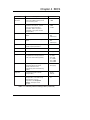
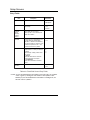
List of Tables
Table 1-1 DRAM Configurations . . . . . . . . . . . . . . . . . . . .1-6
Table 2-1 CPU Jumpers . . . . . . . . . . . . . . . . . . . . . . . . . . .2-2
Table 2-2 J23, DX4 Internal Multiplier . . . . . . . . . . . . . . . .2-2
Table 2-3 J24, 486SL / P24T Write . . . . . . . . . . . . . . . . . .2-3
Table 2-4 J27, Clock Frequency . . . . . . . . . . . . . . . . . . . . .2-3
Table 2-5 J29, CPU Select . . . . . . . . . . . . . . . . . . . . . . . . .2-3
Table 2-6 J34, CPU Functions Enable . . . . . . . . . . . . . . . .2-4
Table 2-7 J35, P24T / Clock Stop . . . . . . . . . . . . . . . . . . . .2-4
Table 2-8 J36, DX / SX Select . . . . . . . . . . . . . . . . . . . . . .2-4
Table 2-9 J37, Cyrix CPU Select . . . . . . . . . . . . . . . . . . . .2-5
Table 2-10 Board Jumpers . . . . . . . . . . . . . . . . . . . . . . . . .2-6
Table 2-11 J1, IDE IRQ Enable . . . . . . . . . . . . . . . . . . . . . .2-6
Table 2-12 J7, IDE Frequency Select . . . . . . . . . . . . . . . . .2-7
Table 2-13 J8, IDE Read Prefetch Enable . . . . . . . . . . . . . .2-7
Table 2-14 J10, IDE Mode Select . . . . . . . . . . . . . . . . . . . .2-7
Table 2-15 J11, IDE Drive Select . . . . . . . . . . . . . . . . . . . .2-8
Table 2-16 J13, Floppy Select . . . . . . . . . . . . . . . . . . . . . .2-8
Table 2-17 J15, Cache Select . . . . . . . . . . . . . . . . . . . . . . .2-8
Table 2-18 J16, SRAM Select . . . . . . . . . . . . . . . . . . . . . .2-9
Table 2-19 J17, CMOS Clear / Battery Enable . . . . . . . . . .2-9
Table 2-20 J18, Mouse IRQ Enable . . . . . . . . . . . . . . . . . . .2-9
iii
Table of Contents
List of Tables (continued)
Table 2-21 J19, Security Password Enable . . . . . . . . . . . . .2-10
Table 2-22 J28, Processor Speed . . . . . . . . . . . . . . . . . . . . .2-10
Table 2-23 J30, Video Enable/Disable . . . . . . . . . . . . . . . . .2-10
Table 2-24 J31, Video IRQ Enable . . . . . . . . . . . . . . . . . . .2-11
Table 2-25 J32, DMA Channel for LPT1 . . . . . . . . . . . . . .2-11
Table 2-26 J39, Video Enable/Disable . . . . . . . . . . . . . . . . .2-11
Table 2-27 Connectors . . . . . . . . . . . . . . . . . . . . . . . . . . . .2-12
Table 2-28 J2, IDE Connector . . . . . . . . . . . . . . . . . . . . . . .2-13
Table 2-29 J3, Floppy Connector . . . . . . . . . . . . . . . . . . . .2-14
Table 2-30 J4, Parallel Port . . . . . . . . . . . . . . . . . . . . . . . . .2-15
Table 2-31 DB25 Connector . . . . . . . . . . . . . . . . . . . . . . . .2-16
Table 2-32 J5, COM1 Port . . . . . . . . . . . . . . . . . . . . . . . . .2-17
Table 2-33 J6, COM2 Port . . . . . . . . . . . . . . . . . . . . . . . . .2-18
Table 2-34 Serial Port Cable Wire List . . . . . . . . . . . . . . . .2-19
Table 2-35 J9, Hard Drive LED Connector . . . . . . . . . . . . .2-20
Table 2-36 J14, Keyboard Connector - 10 pin . . . . . . . . . . .2-20
Table 2-37 J20, Keyboard mini-DIN . . . . . . . . . . . . . . . . . .2-21
Table 2-38 J21, Mouse mini-DIN . . . . . . . . . . . . . . . . . . . .2-21
Table 2-39 J22, Reset Connector . . . . . . . . . . . . . . . . . . . . .2-22
Table 2-40 J25, Speaker Connector . . . . . . . . . . . . . . . . . . .2-22
Table 2-41 J26, CPU Fan Power Connector . . . . . . . . . . . .2-22
Table 2-42 J33, SVGA Connector . . . . . . . . . . . . . . . . . . . .2-23
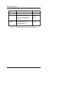
Table 3-1 Environmental Specifications . . . . . . . . . . . . . . .3-2
Table 4-1 Summary Screen Viewing Fields . . . . . . . . . . . . .4-10
Table 4-2 Energy Screen Entry Fields . . . . . . . . . . . . . . . . .4-13
Table 4-3 Clock Screen Entry Fields . . . . . . . . . . . . . . . . . .4-15
Table 4-4 Keyboard Screen Entry Fields . . . . . . . . . . . . . . .4-17
iv
Table of Contents
List of Tables (continued)
Table 4-5 Floppy Screen Entry Fields . . . . . . . . . . . . . . . . .4-19
Table 4-6 Fixed Disk Screen Entry Fields . . . . . . . . . . . . . .4-22
Table 4-7 VL-Bus IDE Screen Entry Fields . . . . . . . . . . . . .4-24
Table 4-8 Boot Sequence Screen Entry Fields . . . . . . . . . . .4-26
Table 4-9 Security Screen Entry Fields . . . . . . . . . . . . . . . .4-28
Table 4-10 Speed Screen Entry Fields . . . . . . . . . . . . . . . . .4-29
Table 4-11 Cache Screen Entry Fields . . . . . . . . . . . . . . . . .4-31
Table 4-12 Shadow RAM Screen Entry Fields . . . . . . . . . . .4-33
Table 4-13 Chipset Screen Entry Fields . . . . . . . . . . . . . . . .4-36
Table 4-14 37C665 Screen Entry Fields . . . . . . . . . . . . . . . .4-38
Table 4-15 Orca Post Codes . . . . . . . . . . . . . . . . . . . . . . . . .4-39
Table 4-16 Diagnostic Port 80h Post Codes . . . . . . . . . . . . .4-41
Table 4-17 Beep Codes and Error Messages . . . . . . . . . . . . .4-42
Table 4-18 Fixed Disk Parameters . . . . . . . . . . . . . . . . . . . .4-44
Table 4-19 Memory Map . . . . . . . . . . . . . . . . . . . . . . . . . . .4-45
Table A1-1 Standard PC-AT I/O Map . . . . . . . . . . . . . . . .A1-1
Table A1-2 DMA Channel Page Register and I/O Add. . . .A1-2
Table A1-3 DMA Channel Assignments . . . . . . . . . . . . . . .A1-2
Table A1-4 DMA Controller Register Functions . . . . . . . . .A1-3
Table A1-5 Interrupts . . . . . . . . . . . . . . . . . . . . . . . . . . . . .A1-4
Table A1-6 CMOS RAM Address Map . . . . . . . . . . . . . . . .A1-5
Table A1-7 Real-Time Clock Information . . . . . . . . . . . . . .A1-6
Table A1-8 ISA Connector Pin Assignments . . . . . . . . . . . .A1-7
v
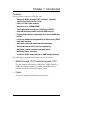
Chapter 1 Introduction
Welcome to the I-Bus family of passive backplane CPU boards.
This manual contains the information necessary to configure your CPU
board to your specific needs.
The Orcaª passive backplane CPU board is IBM
PC/AT- compatible utilizing 5V or 3.3V, 486-compatible processors.
This chapter is divided into three sections:
¥ About this manual
explains how this manual is laid out and what you can expect to
find in it.
¥ Preparing the board
describes the procedure for unpacking the Orca CPU board and
preparing it for use in your system.
¥ Features of the board
provides a brief overview of the major components of the Orca
CPU board accompanied by an illustration of the board showing its
jumpers, connectors and components. For convenient reference, a
fold-out version of this illustration is provided at the back of this
manual.
1-1
About this manual
The first three chapters of this manual pertain to your specific CPU
board. The appendices contain technical reference material, a glossary
of terms, a fold-out illustration of the board, and the BIOS setup utility,
followed by an index.
¥ Chapter 1 Introduction
introduces you to this manual and to the Orca CPU board.
¥ Chapter 2 Jumpers and Connectors
describes the jumpers and connectors on the Orca CPU board.
First, each jumper is described. A table shows on which pins to
place the jumper for your specific configuration and an illustration
of the jumper shows the pin locations. Then, each connector is
described. A table shows the pin-out descriptions and an illustration
shows the pin locations for each connector.
¥ Chapter 3 Specifications
provides the component data and environmental characteristics of
the Orca CPU board.
¥ Appendix 1 Technical Reference
provides additional information that can help you configure your
CPU board and attach external peripheral devices. These include
I/O Maps, I/O Channels, Interrupts and Address Maps and ISA pin
assignments.
¥ Appendix 2 Glossary of Terms
contains definitions of terms used in this manual as well as terms
that refer to items discussed.
¥ Appendix 3 Illustration
provides a convenient fold-out illustration of the Orca CPU board.
¥ Appendix 4 BIOS
explains the setup utility and how to use it.
1-2
Chapter 1 Introduction
¥ Index
provides easy access to page numbers of items discussed.
Preparing the board
¥ Unpacking your CPU board
The Orca CPU board is shipped in a sealed, anti-static shielded bag.
• Open the bag at a static-free workstation while observing proper
Electrostatic Discharge (ESD) practices.
• When not installed in a computer chassis, this board must be
sealed in an ESD approved shielded bag.
• This board must be shipped in a sealed ESD approved shielded
bag and protected with anti-static packaging material (e.g. bubble
wrap).
• I-Bus reserves the right to refuse warranty service on units not
properly packaged to protect against ESD damage.
CAUTION!
Components on this board are sensitive to damage from
Electrostatic Discharge (ESD). Handling of this board should
ONLY be done by a properly trained technician in an approved
ESD work area!
Packaged with the Orca CPU board are:
• an Orca Passive Backplane CPU Board User Manual
• Optional memory
• a Keyboard adapter cable
• Optional cables
If any of the items have been damaged in shipping, notify the transit
company and initiate an insurance claim. If any items are missing,
contact I-Bus. Refer to the Limited Warranty in the back of this
manual for further instructions.
1-3
Features
J14
Keyboard Connector
J20
Keyboard mini-DIN
J18
Mouse IRQ Enable
J21
Mouse mini-DIN
J6
COM2 Port
J5
COM1 Port
J33
SVGA Connector
J39
Video Enable/Disable
J19
Security Password Enable
J4
Parallel Port
J17
Clear CMOS/Battery
Enable
J13
Floppy Select
J32
Select DMA Channel
for LPT1
J12
Reserved
J3
Floppy Connector
J31
Video IRQ Enable
J11
IDE Drive Select
J30
Video Enable/Disable
J10
IDE Mode Select
J9
Hard Drive LED
Connector
J38
Reserved
J16
SRAM Select
J8
IDE Read Prefetch
Enable
J29
CPU Select
J28
Processor Speed
J7
IDE Frequency
Select
J27
Clock Frequency
J2
IDE Connector
J15
Cache Select
J1
IDE IRQ Enable
J24
486SL/P24T Write
SM1
SM2
J23
DX4 Internal Multiplier
J37
Cyrix CPU Select
CPU
SM3
SM4
J36
DX/SX Select
J35
P24T Clock Stop
J22
Reset Connector
J34
CPU Functions Enable
J26
CPU Fan Power Connector
J25
Speaker Connector
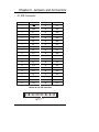
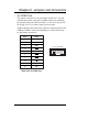
Figure 1-1: Orca CPU Board Jumpers, Connectors,
and Components
1-4
Chapter 1 Introduction
Features
The key features of the Orca CPU board are:
¥ Supports 486SX through P24T Pentiumª Upgrade
Central Processing Units (CPUs)
¥ 256K or 512K cache memory
¥ Supports up to 128MB DRAM
¥ Two high speed serial ports (16550 type UARTS)
¥ One bidirectional parallel port with DMA access
¥ Floppy disk interface supporting up to two 2.88MB disk
drives
¥ Local bus Enhanced Integrated Drive Electronics (EIDE)
hard disk interface
¥ Real-time clock with on-board battery backup
¥ On-board battery with 2 year life expectancy
¥ Keyboard, mouse, speaker, and reset ports
¥ Watchdog timer, two-level
¥ Local bus SVGA video with up to 2MB display memory
The following are detailed descriptions of the above features:
¥ 486SX through P24T Pentium Upgrade CPU
The Orca supports the 486SX @ 25MHz and 33MHz, 486DX @
33MHz and 50MHz, 486DX2 @ 50MHz and 66MHz, DX4 @
100MHz, and the P24T Pentium Upgrade CPUs.
¥ Cache
The Orca is equipped with 256K write back cache.
1-5
Features
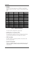
¥ DRAM
The Orca CPU board supports up to 128MB of 72-pin DRAM
SIMMs located in four sockets. Sockets are labeled SM1 through
SM4.
Total
4MB
8MB
16MB
32MB
8MB
16MB
32MB
64MB
128MB
16MB
24MB
40MB
72MB
32MB
48MB
80MB
64MB
96MB
128MB
SM1
---------------------------------------------------------------4MB (1MB x 36)
4MB (1MB x 36)
4MB (1MB x 36)
4MB (1MB x 36)
8MB (2MB x 36)
8MB (2MB x 36)
8MB (2MB x 36)
16MB (4MB x 36)
16MB (4MB x 36)
32MB (8MB x 36)
SM2
---------------------------------------------------------------4MB (1MB x 36)
4MB (1MB x 36)
4MB (1MB x 36)
4MB (1MB x 36)
8MB (2MB x 36)
8MB (2MB x 36)
8MB (2MB x 36)
16MB (4MB x 36)
16MB (4MB x 36)
32MB (8MB x 36)
SM3
----------------------------4MB (1MB x 36)
8MB (2MB x 36)
16MB (4MB x 36)
32MB (8MB x 36)
64MB (16MB x 36)
4MB (1MB x 36)
8MB (2MB x 36)
16MB (4MB x 36)
32MB (8MB x 36)
8MB (2MB x 36)
16MB (4MB x 36)
32MB (8MB x 36)
16MB (4MB x 36)
32MB (8MB x 36)
32MB (8MB x 36)
SM4
4MB (1MB x 36)
8MB (2MB x 36)
16MB (4MB x 36)
32MB (8MB x 36)
4MB (1MB x 36)
8MB (2MB x 36)
16MB (4MB x 36)
32MB (8MB x 36)
64MB (16MB x 36)
4MB (1MB x 36)
8MB (2MB x 36)
16MB (4MB x 36)
32MB (8MB x 36)
8MB (2MB x 36)
16MB (4MB x 36)
32MB (8MB x 36)
16MB (4MB x 36)
32MB (8MB x 36)
32MB (8MB x 36)
Table 1-1: DRAM Configurations
For other possible configurations, contact I-Bus.
¥ Multifunction Controller (XIO)
The multifunction controller provides two high speed serial ports,
one bidirectional parallel port, and a floppy disk controller.
¥ IDE Controller
The IDE controller is supported by VESA 32-bit local bus with
four-level read prefetch.
¥ Serial I/O Interface
There are two RS232-compatible serial communication ports with
16550 type UARTS: a primary serial port at J5 and a secondary
serial port at J6.
1-6
Chapter 1 Introduction
¥ Parallel I/O Interface
The Orca CPU board provides a parallel I/O interface at J4. While
it is conventionally a printer port, it can be reconfigured by software
to be a bidirectional parallel port. Contact I-Bus for information.
¥ Floppy Disk Drive Interface
Any combination of up to two 3.5" and/or 5.25" disk drives or up to
two 2.88MB drives can be installed on the Orca CPU board at J3.
The interface can also be disabled through the BIOS.
¥ OPTi 82C802G
The OPTi 82C802G provides the major portion of the system control. Its features include cache interface, buffer controller, memory
interface, system and cache controllers. The "G" indicates support
for green functions.
¥ Integrated Peripheral Controller (IPC)
The 82C802G integrates two 8237 DMA controllers, two 8259
interrupt controllers and one 8254 timer/counter.
¥ Programmable Interrupt Controller
The 82C802G provides 15 user selectable interrupt channels.
¥ Counter/Timer
The 82C802G provides three independent counter channels.
Counter 0 is used as a system timer. Counter 1 is used to generate
pulses for DRAM refresh. Counter 2 is a full function
counter/timer.
1-7
Features
¥ Direct Memory Access (DMA)
The 82C802G provides seven DMA channels. The first four DMA
channels are used for eight-bit DMA transfers. The remaining three
channels are used for sixteen-bit DMA transfers. The sixteen-bit
DMA channels function identically to the eight-bit DMA channels
except that bit 0 of the address and the length fields are assumed to
be zero. (All transfers must begin on an even address boundary and
the length must be an even number of bytes.) The sixteen-bit DMA
channels transfer up to 128KB while the eight-bit DMA channels
transfer up to 64KB.
¥ IDE Hard Disk Interface
The Orca CPU board provides a Local Bus Enhanced Integrated
Drive Electronics (EIDE) interface for up to two IDE hard disk drives through the header at J2. J2 accepts a forty-pin IDE connector.
¥ Keyboard Interface
The Orca CPU board uses the 8042 keyboard controller. A six-pin
mini-DIN connector is provided at J20. A ten-pin header is also
provided at J14. A keyboard adapter cable is available for keyboards with a five-pin DIN connector. Contact I-Bus for ordering
information.
¥ Real-time Clock/Calendar
The Orca CPU board has a real-time clock/calendar backed by an
on-board battery. It has 114 bytes of CMOS RAM included with
the clock. The battery has a two year life expectancy and is field
replaceable.
¥ Reset
An external reset can be attached to the Orca CPU board through
the connector at J22.
¥ Speaker
The Orca CPU board provides an on-board speaker and the capability of adding an external speaker at connector J25.
1-8
Chapter 1 Introduction
¥ EPROM
The 27C010 EPROM contains the BIOS for the system. The system BIOS is mapped from F0000h to FFFFFh.
¥ Bus Drivers
The Orca CPU board uses buffered bus drivers which are capable of
driving nineteen additional expansion cards.
¥ Watchdog Timer
To operate the watchdog timer on the Orca CPU board, several programming steps are required. After booting the system, perform a
byte write to port 160H to reset the watchdog (data value is unimportant). Set the divisor for the RTC square wave output by performing the following steps:
1. Write a 0AH to port 70H to access port A of the RTC.
2. Read port 71H to retrieve value.
3. Logically OR the value read with 0FH.
4. Write a 0AH to port 70H to access port A of the RTC.
5. Write the modified value to port 71H.
Enable the square wave output by executing the following steps:
1. Write a 0BH to port 70H to access port B of the RTC.
2. Read port 71H to retrieve value.
3. Logically OR the value read with 08H.
4. Write a 0BH to port 70H to access port B of the RTC.
5. Write the modified value to port 71H.
The watchdog timer is now running. To reset the watchdog timer,
perform a byte write to port 160H. The watchdog timer will time
out if no write to port 160H is executed within 16 seconds. At this
point, interrupt 11 is asserted. If another 16 seconds passes without
a write to port 160H the board is reset.
1-9
Features
To disable watchdog timer operation:
1. Write a 0BH to port 70H to access port B of the RTC.
2. Read port 71H to retrieve value.
3. Logically AND the value read with F7H.
4. Write a 0BH to port 70H to access port B of the RTC.
5. Write the modified value to port 71H.
¥ Local Bus Video
The Orca is equipped with on-board local bus SVGA with up to
2MB video RAM. It incorporates the Cirrus Logic CL-GD5434,
and runs at up to 41 million WINMARKS (WINBENCH 3.1) when
using a DX4-100 CPU with 2MB display memory. This provides a
dramatic improvement in performance over ISA video cards.
• Configurable resolutions up to 1280 x 1024 (256 colors noninterlaced)
• 32-bit wide DRAM interface with 1MB; 64-bit wide DRAM
interface with 2MB
• Up to 2MB display memory
• 16.8 million color capability (640 x 480, 800 x 600)
• Backward compatible with VGA, EGA, CGA, MDA
• 15, 16 or 24-bit True Color
• Refresh rates up to 72Hz non-interlaced
• Hardware bit BLT for Microsoft Windows™
• Independent video and DRAM timing
1-10
Chapter 2 Jumpers and Connectors
This chapter describes the jumpers and connectors on the Orca
CPU board. Jumpers and connectors are identified by the label shown
beside them on the board (e.g. J36), followed by the description (e.g.
DX/SX Selection). A table shows the jumper settings or connector pinouts for each jumper and connector. Illustrations of jumpers and connectors are shown from the component side of the board. Pin 1 is identified by the black pin.
All of the jumpers and connectors are shown on the illustration on page
1-4, Figure 1-1, Orca CPU Board Jumpers, Connectors and
Components and on the fold-out illustration on page A3-1.
Pin 1 can be identified on the solder side of the board by the square pad
in a connector or jumper.
For clarity, in this manual jumpers are divided into two types: CPU
Jumpers and Board Jumpers.
• CPU Jumpers, listed in Table 2-1, pertain to settings for the
CPU installed on your CPU board.
• Board Jumpers, listed in Table 2-10, pertain to functions of the
CPU board and its peripherals.
CAUTION!
Components on this board are sensitive to damage from
Electrostatic Discharge (ESD). Handling of this board should
ONLY be done by a properly trained technician in an approved
ESD work area!
2-1
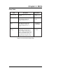
CPU Jumpers
The following jumpers are factory-set for the CPU installed on your
CPU board. If you upgrade to another CPU or reconfigure your system,
you may need to reset some of the jumpers.
Jumper
Description
No. of Pins
J23
DX4 Internal Multiplier
6
J24
486SL/P24T Write
8
J27
Clock Frequency
3
J29
CPU Select
3
J34
CPU Functions Enable
6
J35
P24T/Clock Stop
6
J36
DX/SX Select
4
J37
Cyrix CPU Select
4
Table 2-1: CPU Jumpers
¥ J23, DX4 Internal Multiplier
J23 contains a jumper setting if a Cyrix CPU is present. Otherwise,
the jumper settings pertain to the internal multiplier of the DX4.
Position
Function
3&4
Cyrix CPU-
1&3
DX4 / 2.5X-
3&5
DX4 / 2X-
None
DX4 / 3X-
-
Table 2-2: J23, DX4 Internal Multiplier
2-2
5
3
1
6
4
2
Chapter 2 Jumpers and Connectors
¥ J24, 486SL / P24T Write
Two jumpers must be placed on J24 if your CPU board contains a
486SL CPU (with power management feature). Or, if you have a
P24T CPU installed, you can select burst writes, write-back, or
write-through cache. Removing the jumper from pins 7 and 8
enables the write-through cache for a P24T CPU.
Position
Function
1&2, 3&4
486SL CPU-
5&6
7&8
No Jumpers
Enable P24T Burst WritesEnable P24T Write-BackEnable P24T Write-Through-
1-
2-
3-
4-
5-
6-
7
8
Table 2-3: J24, 486SL / P24T Write
¥ J27, Clock Frequency
J27 contains jumper settings for the slow clock frequency at 8MHz,
or 16MHz for the DX4 CPU.
Position
Function
1&2
8MHz-
2&3
16MHz (DX4)-
321
-
Table 2-4: J27, Clock Frequency
¥ J29, CPU Select
Jumpers must be set on J29 if an Intel/AMD or Cyrix CPU is
present.
Position
1&2
2&3
-
Function
Intel/AMD CPUCyrix CPU-
Table 2-5: J29, CPU Select
2-3
321
CPU Jumpers
¥ J34, CPU Functions Enable
J34 contains a jumper setting to activate the warm reset for a Cyrix
CPU. It also contains a setting if a 486SL CPU (with power management feature) is present. Two settings enable the write-back and
write-through cache for the P24D CPU with special write-back
cache.
Position
4&6
2&4
Function
5
3
1
6
4
2
Activate Cyrix CPU486SL CPU-
3&5
Enable P24D write-back cache-
1&3
Enable P24D write-through cache-
Table 2-6: J34, CPU Functions Enable
¥ J35, P24T / Clock Stop
J35 contains a jumper setting if a P24T CPU is present. Jumpers
are also installed on J35 to select bit 0 or bit 1 of the green port to
stop the clock.
Position
1&3
Function
5
3
1
6
4
2
CPU’s other than P24T-
3&5
P24T-
2&4
Bit 0 to stop clock-
4&6
Bit 1 to stop clock-
Table
2-7: J35, P24T / Clock Stop
¥ J36, DX / SX Select
Set jumpers on J36 for 486DX or 486SX operation.
Position
Function
1&2, 3&4
486DX Operation-
2&3
486SX Operation-
Table
2-8: J36, DX / SX Select
2-4
4
3
2
1
Chapter 2 Jumpers and Connectors
¥ J37, Cyrix CPU Select
Set jumpers on J37 if your CPU board contains a Cyrix CPU.
Position
Function
1&2, 3&4
Cyrix CPU-
OFF
CPU Other than Cyrix-
-
Table 2-9: J37, Cyrix CPU Select
2-5
4
3
2
1
Board Jumpers
The following jumpers control functions of the CPU board and its
peripherals.
Jumper
Description
No. of Pins
J1
IDE IRQ Enable
2
J7
IDE Frequency Select
6
J8
IDE Read Prefetch Enable
3
J10
IDE Mode Select
6
J11
IDE Drive Select
6
J12
Reserved
2
J13
Floppy Select
6
J15
Cache Select
6
J16
SRAM Select
3
J17
Clear CMOS / Battery Enable
3
J18
Mouse IRQ Enable
2
J19
Security Password Enable
2
J28
Processor Speed
6
J30
Video Enable/Disable
3
J31
Video IRQ Enable
2
J32
DMA Channel for LPT1
8
J39
Video Enable/Disable
2
Table 2-10: Board Jumpers
¥ J1, IDE IRQ Enable
Placing a jumper on J1 enables IRQ14 for the IDE. If no jumper is
placed on J1, IRQ14 is available for other use.
Position
Function
1&2
Enable IRQ14-
1-
OFF
IRQ14 Available
2
2-6
Chapter 2 Jumpers and Connectors
¥ J7, IDE Frequency Select
This jumper setting must match the frequency of the CPU installed
on your CPU board.
Position
Function
4&6, 3&5
50MHz-
3&5, 2&4
40MHz-
1&3, 4&6
33MHz-
1&3, 2&4
25MHz-
5
3
1
6
4
2
Table
2-12: J7, IDE Frequency Select
¥ J8, IDE Read Prefetch Enable
Read prefetch allows the controller to access data off the disk in
anticipation of its use.
Note: If WindowsNT™ is being used, jumpers must be placed on
pins 2 and 3 for proper operation.
Position
Function
1&2
Enable IDE Read Prefetch-
2&3
Disable IDE Read Prefetch
1
2
3
Table 2-13: J8, IDE Read Prefetch Enable
¥ J10, IDE Mode Select
Select the appropriate disk drive cycle time by placing jumpers on
the designated pins.
Position
Function
3 & 5, 4 & 6
> 480ns
1 & 3, 4 & 6
> 383ns
3 & 5, 2 & 4
> 240ns
1 & 3, 2 & 4
> 180ns
Table 2-14: J10, IDE Mode Select
2-7
5
3
1
6
4
2
Board Jumpers
¥ J11, IDE Drive Select
Select the address for the IDE port. Either one or the other must be
installed unless it is disabled.
Position
Function
1&3
Primary IDE-
3&5
Secondary IDE-
2&4
Enable IDE port-
4&6
Disable IDE port-
5
3
1
6
4
2
-
Table 2-15: J11, IDE Drive Select
¥ J12, Reserved - no jumper
¥ J13, Floppy Select
Select the density of the floppy disk drive enabled in the BIOS.
Position
Function
1&2
1.44MB-
3&4, 5&6
2.88MB
Table 2-16: J13, Floppy Select
5
3
1
6
4
2
¥ J15, Cache Select
Place the jumper on the designated pins for the amount of cache on
your CPU board.
Position
no jumpers
5&6
3&4, 5&6
1&2,3&4,5&6
-
Function
64K-
1-
2-
128K-
3-
4-
256K-
5
6
512K-
Table 2-17: J15, Cache Select
2-8
Chapter 2 Jumpers and Connectors
¥ J16, SRAM Select
J16 contains jumper settings for single bank SRAMs or double bank
SRAMs in the cache.
Position
Function
1&2
Single Bank (4)-
2&3
Double Bank (8)
123
Table 2-18: J16, SRAM Select
¥ J17, CMOS Clear / Battery Enable
J17 contains jumper settings for clearing the system information
stored in CMOS and enabling the on-board battery.
Position
Function
1&2
Clear CMOS-
3-
2&3
Enable Battery
21
Table 2-19: J17, CMOS Clear / Battery Enable
¥ J18, Mouse IRQ Enable
Placing a jumper on J18 enables IRQ12 for the mouse. If no
jumper is placed on J18, the mouse is disabled and IRQ12 is available for other use.
Position
Function
1&2
IRQ12 Enabled
OFF
IRQ12 Available
1-
Table 2-20: J18, Mouse IRQ Enable
2-9
2
Board Jumpers
¥ J19, Security Password Enable
Installing a jumper on pins 1 and 2 of J19 enables the security password option in the BIOS Setup Utility. With this jumper installed,
the password selection is available in BIOS.
Position
Function
1&2
Password Enabled
OFF
Password Disabled
21
Table 2-21: J19, Security Password Enable
¥ J28, Processor Speed
Select the clock speed of your CPU.
Position
5&6
Function
25MHz-
1&2, 5&6
33MHz-
3&4, 5&6
40MHz-
1&2,3&4,5&6
6-
5-
4-
3-
2
1
50MHz-
-
Table 2-22: J28, Processor Speed
¥ J30, Video Enable/Disable
Installing a jumper on pins 2 and 3 enables the on-board video controller. To disable the on-board video controller, install the jumper
on pins 1 and 2. This video selection (video enabled or disabled)
must be the same as jumper J39.
Position
Function
1&2
Video Disabled
2-
2&3
Video Enabled
3
Table 2-23: J30, Video Enable/Disable
2-10
1-
Chapter 2 Jumpers and Connectors
¥ J31, Video IRQ Enable
Placing a jumper on J31 enables IRQ9 for video. If no jumper is
placed on J31, IRQ9 is available for other use.
Position
Function
1&2
IRQ9 Enabled
2-
OFF
IRQ9 Available
1
Table 2-24: J31, Video IRQ Enable
¥ J32, DMA Channel for LPT1
Using DMA Channels enables high speed transfers from memory to
the parallel port. You can select DMA Channels 1 or 3 to be used
for the parallel port.
Position
Function
8-
7-
1&2, 7&8
DMA Channel 3-
6-
5-
3&4, 5&6
DMA Channel 1
4-
3-
2
1
Table 2-25: J32, DMA Channel for LPT1
¥ J39, Video Enable/Disable
Installing a jumper on pins 1 and 2 enables the on-board video controller. To disable the on-board video controller, remove the
jumper. This video selection (video enabled or disabled) must be
the same as jumper J30.
Position
Function
1&2
Video Enabled
OFF
Video Disabled
Table 2-26: J39, Video Enable/Disable
2-11
12
Connectors
The following connectors can be located in Figure 1-1: ORCA CPU
Board Jumpers, Connectors and Components on page 1-4 and on
the fold-out illustration at the back of this manual.
Jumper
Description
No. of Pins
J2
IDE Connector
40
J3
Floppy Connector
34
J4
Parallel Port
26
J5
COM1 Port
10
J6
COM2 Port
10
J9
Hard Drive LED Connector
2
J14
Keyboard Connector - 10 pin
J20
Keyboard mini-DIN
6
J21
Mouse mini-DIN
6
J22
Reset Connector
2
J25
Speaker Connector
4
J26
CPU Fan Power Connector
4
J33
SVGA Connector
Table 2-27: Connectors
2-12
10
15
Chapter 2 Jumpers and Connectors
¥ J2, IDE Connector
Pin #
Name
Pin #
Name
1
RST
21
N/C
2
GND
22
GND
3
D7
23
IOW
4
D8
24
GND
5
D6
25
IOR
6
D9
26
GND
7
D5
27
N/C
8
D10
28
BALE
9
D4
29
N/C
10
D11
30
GND
11
D3
31
IRQ14
12
D12
32
IO16
13
D2
33
SAI
14
D13
34
N/C
15
D1
35
SA0
16
D14
36
SA2
17
D0
37
CS0
18
D15
38
CS1
19
GND
39
HDIND
20
Key
40
N/C
Table 2-28: J2, IDE Connector
2
40
1
39
Indicates connector
key position
2-13
Connectors
¥ J3, Floppy Connector
Pin #
Name
2
RMP/LC
4
N/C
6
ID0
8
INDEX
10
MTRO
12
DRV1
14
DRV0
16
MTR1
18
DIR
20
STEP
22
WDATA
24
WGATE
26
TRK0
28
WPRT
29
ID0
30
RDATA
32
HDSEL
33
ID1
34
DSKCHG
*
GND
Table 2-29: J3, Floppy Connector
* The remainder of the odd numbered pins are GND.
2
34
1
33
2-14
Chapter 2 Jumpers and Connectors
¥ J4, Parallel Port
Pin #
Name
Pin #
Name
1
Strobe
2
AutoFeed
3
+ Data bit 0
4
Error
5
+ Data bit 1
6
Init
7
+ Data bit 2
8
SLCT IN
9
+ Data bit 3
10
GND
11
+ Data bit 4
12
GND
13
+ Data bit 5
14
GND
15
+ Data bit 6
16
GND
17
+ Data bit 7
18
GND
19
ACK
20
GND
21
Busy
22
GND
23
Paper Empty
24
GND
25
GND
26
N/C
Table 2-30: J4, Parallel Port
2
26
1
25
2-15
Connectors
¥ DB25 Connector
The optional parallel port cable connects to J4 on the CPU board and
contains a DB25 connector which attaches to the I/O panel on the back
of the chassis.
Pin#
Name
1
-Strobe-
2
+Data bit 0-
3
+Data bit 1-
4
+Data bit 2-
1-
5
+Data bit 3-
6
+Data bit 4-
7
+Data bit 5-
-
8
+Data bit 6-
-
9
+Data bit 7-
-
10
ACK1-
-
11
Busy-
-
12
Paper Empty-
13
14
SLCTAutoFeed-
15
Error-
16
Init-
17
SLCT IN-
18-25
GND-
Table 2-31: DB25 Connector
2-16
-
13
1425
Chapter 2 Jumpers and Connectors
¥ J5, COM1 Port
The primary serial port is a ten-pin header located at J5. You can
terminate the primary serial port in a DB9 connector by obtaining
the optional serial port cable from I-Bus. A wire list is also provided on page 2-19 if you want to make your own cable.
Another optional cable from I-Bus contains a retaining bracket with
a DB9 and a DB25 connector terminating in a ten-pin and twentysix-pin header, respectively.
Pin #
Name
1
DCD
2
DSR
3
RXD
4
RTS
5
TXD
6
CTS
7
DTR
8
RI
9
GND
10
N/C
2 4 6 8 10
1 3 5 7 9
Table 2-32: J5, COM1 Port
2-17
Connectors
¥ J6, COM2 Port
The secondary serial port is a ten-pin header located at J6. You can
terminate the secondary serial port in a DB9 connector by obtaining
the optional serial port cable from I-Bus. A wire list is also provided on page 2-19 if you want to make your own cable.
Another optional cable from I-Bus contains a retaining bracket with
a DB9 and a DB25 connector terminating in a ten-pin and twentysix-pin header, respectively.
Pin #
Name
1
DCD
2
DSR
3
RXD
4
RTS
5
TXD
6
CTS
7
DTR
8
RI
9
GND
10
N/C
2 4 6 8 10
1 3 5 7 9
Table 2-33: J6, COM2 Port
2-18
Chapter 2 Jumpers and Connectors
¥ Serial Port Cable Wire List
The following wire list is provided for users who want to make a
cable that connects to a serial port connector (J5 or J6) and terminates with either a DB9 or DB25 (RS232) connector. For the locations of J5 and J6, refer to Figure 1-1, ORCA CPU Board
Jumpers, Connectors and Components on page 1-4.
Signal
Name
Connector
Onboard 10 Pin
Connector (J5 or J6)
25 Pin
9 Pin
DCD
1
8
1
DSR
2
6
6
RXD
3
3
2
RTS
4
4
7
TXD
5
2
3
CTS
6
5
8
DTR
7
20
4
RI
8
22
9
GND
9
2
5
N/C
10
N/C
N/C
Table 2-34: Serial Port Cable Wire List
The following cable assembly shows the Pin 1 locations for the
DB9 and ten-pin connectors. Serial port cables with DB9 and
DB25 connectors are also available through I-Bus.
Pin 1
10-pin Connector
DB9 Connector
2-19
Connectors
¥ J9, Hard Drive LED Connector
An LED can be connected at J9 to display hard drive activity.
Pin#
Name
2
Anode-
1
Cathode
-
12
Table 2-35: J9, Hard Drive LED Connector
¥ J14, Keyboard Connector - 10-pin
Pin #
Name
1
CLOCK
2
GND
3
DATA
4
N/C
5
N/C
6
N/C
1 3 5 7 9
7
+5 V
Indicates connector
key position
8
Key
9
N/C
10
GND
Table 2-36: J14, Keyboard Connector - 10-
2-20
2 4 6 8 10
Chapter 2 Jumpers and Connectors
¥ J20, Keyboard mini-DIN
J20 is a six-pin mini-DIN keyboard connector located on the retaining bracket. You can also use a standard PC/AT-compatible keyboard fitted with the keyboard adapter cable furnished with your
CPU board. Or, you can use the ten-pin keyboard header at J14.
Pin #
Name
1
DATA
2
N/C
3
GND
4
+5 V
5
CLOCK
6
N/C
6
5
4
3
2
1
View from end
of board
Table 2-37: J20, Keyboard mini-DIN
CAUTION!
The mouse and keyboard mini-DIN connectors are
identical. Make sure the correct accessory is plugged
into it’s proper connector.
¥ J21, Mouse mini-DIN
J21 is a six-pin mini-DIN mouse connector located on the retaining
bracket.
Pin #
Name
1
DATA
2
N/C
3
GND
4
+5 V
5
CLOCK
6
N/C
Table 2-38: J21, Mouse mini-DIN
2-21
6
5
4
3
2
1
View from end
of board
Connectors
¥ J22, Reset Connector
An external reset cable can be attached to the ORCA at J22.
Pin#
Name
2
Reset-
1
GND
-
12
Table 2-39: J22, Reset Connector
¥ J25, Speaker Connector
Placing a jumper on pins 1 and 2 of J6 enables the on-board speaker. You can attach an external speaker to the ORCA by connecting
a four position connector to J25.
Pin#
Name
1
External Speaker-
2
Internal Speaker-
3
VCC-
4
VCC-
4
3
2
1
Table 2-40: J25, Speaker Connector
¥ J26, CPU Fan Power Connector
You can connect a CPU fan by connecting a four-position connector
to J26.
Pin#
Name
1
+12V-
2
N/C-
3
N/C-
4
GND-
Table 2-41: J26, CPU Fan Power Connector
2-22
4
3
2
1
Chapter 2 Jumpers and Connectors
¥ J33, SVGA Connector
J33 is a 15-pin connector located on the retaining bracket and connecting the SVGA with the system monitor.
Pin#
Name
1
Red Drive-
2
Green Drive-
3
Blue Drive-
4
N/C-
5
GND-
5-
6
GND-
-
7
GND-
8
GND-
9
N/C-
10
GND-
11
N/C-
12
N/C-
13
HORIZ SYNC-
14
VERT SYNC-
15
N/C-
Table 2-42: J33, SVGA Connector
2-23
6
123410
1112131415
Chapter 3 Specifications
System Components
CPU:
486SX/33 & 100,
486DX/50 & 66, DX4, P24T
Form Factor:
Standard full length AT
Interrupts:
15 levels available
Power Requirements:
Input Power with DX4-100 CPU and
4MB DRAM
+5V @ 4.6A
+12V @ 50mA
-12V @ 50mA
Cache:
256K or 512K standard write-back
cache
Dynamic RAM:
2MB to 128MB on-board 36-bit
DRAM SIMM
System ROM:
Contains system & video BIOS
Clock/Calendar:
Real-time clock backed by an on-board
lithium battery
External Connections:
IDE & floppy (shrouded headers)
Bidirectional parallel port (shrouded
header)
Serial port 1 (shrouded header)
Serial port 2 (shrouded header)
Keyboard (mini-DIN on retaining
bracket)
PS/2 Mouse (mini-DIN on retaining
bracket)
Keyboard (Ten-pin header)
Speaker (header)
Reset (header)
Hard Drive LED (header)
SVGA (15-pin connector on retaining
bracket)
Watchdog Timer:
Two-stage, software programmable
3-1
Environmental Specifications
SVGA Connector: Configurable resolutions up to 1280 x 1024
(256 colors non-interlaced)
32-bit wide DRAM interface with 1MB display
memory
64-bit wide DRAM interface with 2MB display
memory
Up to 2MB display memory
16.8 million color capability (640 x 480, 800 x
600)
Backward compatible with VGA, EGA, CGA,
MDA
15, 16 or 24-bit True Color
Refresh rates up to 72Hz non-interlaced
Hardware bit BLT for Microsoft Windows™
Independent video and DRAM timing
Environmental Specifications
Environmental
Operating
Temperature
0° to +55°C
Non-operating
-40° to +65°C
Humidity
5 to 95% @ 40°C
non-condensing
5 to 95% @ 40°C
non-condensing
Shock
2.5 g @ 10 ms
10 g @ 10 ms
Vibration
0.25 g @ 5-100 Hz
5 g @ 5-100 Hz
Table 3-1: Environmental Specifications
Agency
All I-Bus CPU boards meet UL 1950, CSA 22.2 No. 950, TUV and IEC
950, and FCC Part 15 Class A in I-Bus enclosures. Customer requested
FCC, VDE and CISPR Class B certification available.
3-2
Chapter 4 BIOS
The BIOS Setup Utility allows you to configure your CPU
(Central Processing Unit) board to your system. The BIOS, or Basic
Input/Output System, is the on-board firmware that communicates with
the display, keyboard, printers and other peripheral devices.
Starting and Exiting the BIOS Setup
When you turn on your computer, a test is conducted called the Power
On Self Test, or POST. During this test the system checks for certain
hardware configurations and compares them to the BIOS Setup Utility.
If, at boot, the system status does not match the system configuration
stored in CMOS, you will be prompted to start the BIOS Setup Utility.
This occurs if the "Initialization Errors Halt" prompt is set to "Active"
in the Boot Sequence setup screen. If set to "Inactive,” the system continues to boot.
To Start the BIOS Setup:
•
During a cold boot, press <Esc> while the memory size is
scrolling on the screen.
•
While in DOS, press <Ctrl> + <Alt> + <Esc>. (When you exit
the BIOS, the system automatically reboots).
To Exit the BIOS Setup and boot the computer:
•
While in a utility screen, move the cursor to the menu line at
the top of any screen and press <F10>. All configuration
changes edited in the various screens are recorded in CMOS
memory at this time. If, however, you turn off the power or
press the front panel reset button without pressing <F10>, the
changes you made in the BIOS will not be saved and the original configuration will remain unchanged.
4-1
Operating the BIOS Setup
The screens presented in this manual reflect the same format as your
screens but they do not contain parameters.
¥ All BIOS screens contain:
•
menu line at the top of the screen containing names of the utilities available from that screen.
•
body consisting of the entry fields containing the utility's parameters.
•
bottom line indicating the keystrokes that you can use to
manipulate the cursor in that screen.
¥ Manipulating the screens
A reverse video cursor is always present, either on the menu line or in
the body.
•
Use the <Right Arrow> and <Left Arrow> keys to move the
cursor across the menu line, highlighting the name of the current utility.
•
When a utility's name is highlighted in the menu line, the entry
fields of that utility are displayed in the body. Press the <Down
Arrow> key to move the cursor into the first entry field. You
can move the cursor through the entry fields using the <Down
Arrow> key.
•
To change an entry field, press <Enter>, then follow the instructions in the bottom line. The instructions change depending on
the current field.
•
You can scroll through the available choices for that field by
pressing the <Spacebar> or the "+" and "-" keys in all
adjustable fields. A few fields require alphanumeric entry.
•
When all changes have been made to the entry fields, press
<Esc> to return the cursor to the menu line. The bottom line
changes back to its previous condition.
•
When the cursor is in the menu line, you can press <F10> to
save your changes and reboot the computer.
4-2
Chapter 4 BIOS
¥ Keystrokes
The following keys are available while the cursor is on the menu
line:
Keystroke
Movement
Right, Left Arrow
right and left movement
Space, BackSpace
right and left movement
Tab, Shift-Tab
right and left movement
Home, End
leftmost and rightmost entry
DownArrow, Enter, PgDn
move down into edit window
F10
record and exit Setup
The following keys are generally available within the body:
Movement
Keystroke
Arrows
up, down, left, right
Space, BackSpace
scroll choices in field
Plus, Minus
scroll choices in field
AlphaNumeric
letters and numbers
Enter, (Esc)
begin/end (abort) mode or A/N entry
Esc, PgUp
exit current window, go back to menu
4-3
Your System's Parameters
Once you have set your system's parameters, record the settings below.
If for any reason you should lose the parameter settings on your system
(e.g. the CMOS is reset), you will then be able to easily re-enter them.
Summary
CPU Type
____________
Floppy 0
____________
CPU Rev
____________
Floppy 1
____________
CPU MHz
____________
Floppy 2
____________
PLL Ratio
____________
Floppy 3
____________
CPU Code Cache __________
Fixed 80
____________
CPU Data Cache ___________
Fixed 81
____________
External Cache ____________
Keyboard
____________
Memory - Base ____________
NumLock
____________
Memory - System __________
PS2-Mouse
____________
Memory - Extended ________
Video-Primary ____________
Memory - Total ____________
Video-Secondary ___________
Chipset
____________
BIOS ID
____________
BIOS Date
____________
Energy
IDE Drive Timer ___________
Event Monitoring ___________
System Activity ___________
Idle Video State
___________
Clock
Display Format ____________
Date
Time
Daylight Savings ___________
___________________
4-4
____________
Chapter 4 BIOS
Keyboard
NumLock State at Bootup
___________
Keyboard Typematic Speed
___________
Delay Before Keys Repeat
___________
Floppy
Floppy 0
___________
Floppy 2
___________
Floppy 1
___________
Floppy 3
___________
Step-Rate
___________
Fixed Disk 80
Size
Fixed Disk 81
___________
___________
Type
___________
Cylinders
___________
Heads
___________
Precomp
___________
Landing
___________
Sectors
___________
___________
Translate
___________
Xfer-Mode
___________
Anti-Virus
___________
Size
___________
___________
Type
___________
Cylinders
___________
Heads
___________
Precomp
___________
Landing
___________
Sectors
___________
___________
4-5
Translate
___________
Xfer-Mode
___________
Your System's Parameters
VL-Bus IDE
Drive 80 (C:)
___________
Selectable Rate ___________
Drive 81 (D:)
___________
External Jumper __________
VL-Bus (LRDY) ___________
Boot Sequence
Operating System
___________
Boot Sequence
___________
Memory Priming
___________
Cold-Boot Delay
___________
Initialization Error Halts___________
Ports
COM 1
___________
LPT1
___________
COM 2
___________
LPT 2
___________
COM 3
___________
LPT 3
___________
COM 4
___________
LPT 4
___________
Security
Security
___________
Speed
System Speed ___________
Cache
486-CPU Cache___________
SRAM Write Cycle
___________
External Cache ___________
Shadow RAM
___________
SRAM Burst Read__________ Cache Size
4-6
___________
Chapter 4 BIOS
Shadow RAM
___________
D000 Adapter ___________
E000 Adapter ___________
CC00 Adapter ___________
DC00 Adapter ___________
C800 Adapter ___________
D800 Adapter ___________
C400 Video
___________
D400 Adapter ___________
C000 Video
___________
F000 System
Chipset
Memory Timing
Wait States - Read___________
A20-Gate Control___________
Wait States - Write___________
Memory Refresh
Method ___________________
Period_____________________
AT-BUS Timing
Wait States__________________
I/O Recovery_______________
AT-Bus Clock_______________
37C665
Primary Serial
___________
Parallel Port
___________
Secondary Serial
___________
Floppy
___________
4-7
Setup Screens
This section
describes each setup screen in the Orca BIOS Setup
Utility.
Screens are identified in the menu line as:
• Summary
¥ Ports
¥ Energy
¥ Security
¥ Clock
¥ Speed
¥ Keyboard
¥ Cache
¥ Floppy
¥ Shadow RAM
¥ Fixed Disk
¥ Chipset
¥ VL-Bus IDE
¥ 37C665
¥ Boot Sequence
In this section each utility is represented by:
• Screen Illustration
¥ Explanation
¥ Entry Fields
Screen Illustration
The screens presented in this manual reflect the same format as your
screens but they do not contain parameters.
Explanation
The Explanation following each screen illustration describes the utility
and the available choices.
Entry Fields
Each entry field in the body of the screen is described and all available
choices, or parameters, are listed in table form.
4-8
Chapter 4 BIOS
¥ Summary Screen
Summary
Energy
Clock
Keyboard
CPU Type . . . . . . . . . . . . . . . . . . . . . . . . .
CPU Rev . . . . . . . . . . . . . . . . . . . . . . . . . .
CPU MHz . . . . . . . . . . . . . . . . . . . . . . . . .
PLL Ratio . . . . . . . . . . . . . . . . . . . . . . . . .
CPU Code Cache . . . . . . . . . . . . . . . . . . .
CPU Data Cache . . . . . . . . . . . . . . . . . . . .
External Cache . . . . . . . . . . . . . . . . . . . . .
Memory - Base . . . . . . . . . . . . . . . . . . . . . .
Memory - System . . . . . . . . . . . . . . . . . . . .
Memory - Extended . . . . . . . . . . . . . . . . . .
Memory - Total . . . . . . . . . . . . . . . . . . . . .
COM1 . . . . . . . . . . .
COM2 . . . . . . . . . . .
COM3 . . . . . . . . . . .
COM4 . . . . . . . . . . .
LPT1 . . . . . . . . .
LPT2 . . . . . . . . .
LPT3 . . . . . . . . .
LPT4 . . . . . . . . .
Floppy
Fixed Disk
More ----
Chipset . . . . . . . . . . . . . . . . . . . . . . . . . .
BIOS ID . . . . . . . . . . . . . . . . . . . . . . . . .
BIOS Date . . . . . . . . . . . . . . . . . . . . . . .
Floppy 0 . . . . . . . . . . . . . . . . . . . . . . . . .
Floppy 1 . . . . . . . . . . . . . . . . . . . . . . . . .
Floppy 2 . . . . . . . . . . . . . . . . . . . . . . . . .
Floppy 3 . . . . . . . . . . . . . . . . . . . . . . . . .
Fixed 80 . . . . . . . . . . . . . . . . . . . . . . . . .
Fixed 81 . . . . . . . . . . . . . . . . . . . . . . . . .
Keyboard . . . . . . . . . . . . . . . . . . . . . . . .
NumLock . . . . . . . . . . . . . . . . . . . . . . . .
PS2-Mouse . . . . . . . . . . . . . . . . . . . . . . .
Video-Primary . . . . . . . . . . . . . . . . . . . .
Video-Secondary . . . . . . . . . . . . . . . . . .
F10 to Record and Exit
Home End Moves Cursor
Figure 4-1: Summary Screen
Explanation
The Summary Screen contains information about the hardware on your
system. No user entry is allowed.
This screen allows you to view system information and indicates when
a system component has been properly installed and recognized by the
BIOS.
Some of the items on this screen are auto-sensed during the Power On
Self Test (POST). Others are determined by selections you make on the
following screens.
Items that are auto-sensed are:
CPU Type and MHz
Memory Base and Total
CPU Rev
Video Type
CPU Code Cache
Keyboard Type
CPU Data Cache
Floppy
RAM Cache
Fixed Disk
4-9
Setup Screens
Review this screen after making configuration changes and prior to exiting the Setup Utility.
Viewing Fields
There is no user entry allowed on this screen.
The parameters displayed are auto-sensed during POST or they are
selectable on other screens.
If the BIOS recognizes any serial and parallel ports, their addresses will
appear next to the port. If not, "n/a" will appear.
Field
Description
Parameters
CPU Type
Part number of the
microprocessor installed in your
system (auto-sensed during
POST).
1. 486DX4
2. P24T
CPU Rev
Revision level of the CPU (autosensed during POST).
1. 0480
CPU MHz
Operating frequency (auto-sensed
during POST).
1. 99.7
PLL Ratio
The factor by which the external
operating frequency of the system
board is multiplied to obtain the
internal CPU MHz.
1. 1:1
2. 2:1
3. 3:1
CPU Code
Cache
Amount of internal CPU cache
allocated for code.
1. 8K
CPU Data
Cache
Amount of internal CPU cache
allocated for data instructions.
1. 8K
External Cache
How much cache is on the CPU
board.
1. 256K
2. 512K
Memory - Base
The amount of Base Memory (at
and below the 640K boundary)
found to be in working order
(auto-sensed during POST).
1. 640K
Memory System
A portion of memory, typically
384K, reserved for special uses.
Some may be allocated to
Shadow RAM, and the remainder
might automatically be remapped
to the Extended Memory pool.
This field shows the amount of
memory retained for system use.
1. 384K
Table 4-1: Summary Screen Viewing Fields
4-10
Chapter 4 BIOS
Field
Description
Parameters
Memory Extended
The amount of Extended Memory
(above the 1MB boundary) found
to be in working order.
1. 3 MB
2. 7 MB
Memory - Total
The total amount of memory
installed in the system. It is the
sum of the three preceding
quantities: Base + System +
Extended = Total (auto-sensed
during POST).
1. 4 MB
2. 8 MB
3. 16 MB
COM1 - 4
Serial ports auto-sensed by the
BIOS.
1. n/a
2. Port
address(es)
LPT1 - 4
Parallel ports auto-sensed by the
BIOS.
1. n/a
2. Port
address(es)
Chipset
Permits optional fine tuning of
certain chipset parameters.
Opti 802G
BIOS ID
BIOS Type.
OptI9CI
BIOS Date
Date BIOS was built.
mm/dd/yy
Floppy 0 - 3
The floppy drives configured in
the system and usually named A
or B (auto-sensed during POST).
1.
2.
3.
4.
5.
6.
Fixed 80 - 81
The configured Size and Type for
Fixed Disk Drives 80 and 81,
usually named C and D,
respectively (auto-sensed during
POST).
1. None
2. Size [type]
Keyboard
Keyboard type (auto-sensed
during POST).
1. PC/AT
2. AT/PS2
NumLock
The NumLock state (auto-sensed
during POST). This field is only
meaningful for 101 key
keyboards. See Keyboard
Screen description in this
Chapter.
1. Off
2. On
None
5¼, 360K
3½, 720K
5¼, 1.2MB
3½, 1.4MB
3½, 2.8MB
Table 4-1: Summary Screen Viewing Fields (continued)
4-11
Setup Screens
Field
Description
PS2-Mouse
Parameters
1. n/a
Video - Primary
The main video display adapter
which will be in use when control
is passed to an Operating System
at power-up (auto-sensed during
POST).
1. None
2. V/EGA Color
3. Mono
Video Secondary
Indicates the presence of a
second video adapter. It will
remain idle until activated by
specialized software.
1. n/a
2. Mono
Table 4-1: Summary Screen Viewing Fields (continued)
4-12
Chapter 4 BIOS
¥ Energy Screen
Summary
Energy
Clock
Keyboard
Floppy
Fixed Disk
More ----
Energy Management Idle Timers
IDE Drive Timer . . . . . . . . . . . . 1 Min
System Activity . . . . . . . . . . . . . 2 Min
* Event Monitoring . . . . . . . . . . . Local
* Idle Video State . . . . . . . . . . . . . Off
* Default
F10 to Record and Exit
Home End Moves Cursor
Figure 4-2: Energy Screen
Explanation
Options available on this screen enable the user to reduce power consumption when the system is idle.
Entry Fields
Field
Description
Parameters
IDE Drive Timer
This switch can be set to 1, 2, or 5
minutes. After this duration with
no activity, the hard drive is spun
down.
1. 1, 2 or 5
minutes.
System Activity
After the above time has elapsed
with no activity, the system
operating frequency is reduced to
8 or 16MHz depending upon the
CPU.
1. 2, 5, 15, 30,
40, 60, 240
minutes.
Event
Monitoring
"Local" corresponds to the
keyboard input.
1. Local
2. Global
Idle Video State
When the system goes to slow
speed operation, the screen
blanks if this is set to "Off ."
1. On
2. Off
Table 4-2: Energy Screen Entry Fields
4-13
Setup Screens
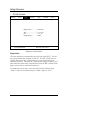
¥ Clock Screen
Summary
Energy
Clock
Keyboard
Floppy
Fixed Disk
More ----
Display Format . . . . . . . . . . . . United States
Time . . . . . . . . . . . . . . . . . . . . . 12 : 16 : 19 p
Date . . . . . . . . . . . . . . . . . . . . . 11 / 1 / 96
Daylight Savings . . . . . . . . . . . Disable
F10 to Record and Exit
Home End Moves Cursor
Figure 4-3: Clock Screen
Explanation
The time and date are maintained in the real-time clock (RTC). It's battery powered when the computer is shut off. The RTC needs to be set
with the initial time/date. Adjustments are required periodically for
continued accuracy. Variations in voltage (power supply or battery) and
other technical issues make it impractical to tune the RTC with the same
degree of precision as a dedicated timepiece.
To change the time or date, move the cursor into the field and press
<Enter>. Enter the new data and press <Enter> again or <Esc>.
4-14
Chapter 4 BIOS
Entry Fields
Field
Description
Parameters
Display Format
Select the display format for time
and date.
1. U.S.
2. International
Time
Press <Enter> and move the
cursor under the number to
change and enter "0-9" or "+"
or "-".
1. 12hr am/pm
2. 24hr
Date
Press <Enter> and move the
cursor under the number to
change and enter "0-9" or "+"
or "-".
1. mm/dd/yyyy
2. dd/mm/yyyy
Daylight
Savings
The RTC can be instructed to
automatically correct the time on
the two daylight savings days of
the year. Altering this field will not
cause an immediate change. The
RTC adjusts the time only when a
daylight savings transition occurs.
1. Enable
2. Disable
Table 4-3: Clock Screen Entry Fields
4-15
Setup Screens
¥ Keyboard Screen
Summary
Energy
Clock
Keyboard
Floppy
Fixed Disk
More ----
NumLock State at Bootup . . . . . .
Keyboard Typematic Speed . . . . .
Delay Before Keys Repeat. . . . . . .
F10 to Record and Exit
Home End Moves Cursor
Figure 4-4: Keyboard Screen
Explanation
From this screen you can control the power-up state of NumLock,
Keyboard Typematic Speed and Delay Before Repeat.
NumLock State at Bootup. This parameter sets the Numlock state of
the numeric keypad of your keyboard at power-up. You can change it at
any time by pressing the NumLock key.
When set to "Off," the numeric keys will produce special control functions (PgUp, PgDn, Home, End, Ins, Del, and cursors). When set to
"On," the numeric keys will produce the indicated numbers.
Keyboard Typematic Speed. This is the rate in characters-per-second
at which a key will repeat when depressed.
Delay Before Keys Repeat. This is the length of time a key can be
depressed before it will begin to repeat.
4-16
Chapter 4 BIOS
Entry Fields
Field
Description
Parameters
NumLock State
at Bootup
The initial NumLock state is
programmable for cursor or
numeric operation. "On" selects
numeric entry and "Off" selects
cursor control.
1. On
2. Off
Keyboard
Typematic
Speed
Select the default rate of 10cps or
select from 2 cps to 30 cps.
1. Default
2. 2.0-30.0 cps
Delay Before
Keys Repeat
Select one of four settings
between 0.25 to 1.0 seconds that
comfortably allows you to release
the keys before they begin to
repeat.
Note: This field will display
"Default" and cannot be changed
if the "Keyboard Typematic
Speed" field is set to "Default ."
1. Default
2. 0.25-1.0 sec
Table 4-4: Keyboard Screen Entry Fields
4-17
Setup Screens
¥ Floppy Screen
Summary
Energy
Clock
Keyboard
Floppy
Fixed Disk
More ----
Floppy Drive Configuration
Floppy 0 . . . . . . . . . . . . . . .
Floppy 1 . . . . . . . . . . . . . . .
Floppy 2 . . . . . . . . . . . . . . .
Floppy 3 . . . . . . . . . . . . . . .
Step Rate . . . . . . . . . . . . . . .
F10 to Record and Exit
Home End Moves Cursor
Figure 4-5: Floppy Screen
Explanation
Your system can have as many as four floppy disk drives, referred to as
Floppy 0 through Floppy 3, corresponding to A:, B:, etc., respectively,
depending on your operating system. Each floppy drive in your system
must be identified as one of the following:
• 5⁄
360K low density
• 3 fi
720K low density
• 5⁄
1.2MB high density
• 3 fi
1.4MB high density
• 3 fi
2.8MB extra density
The BIOS will support:
2.88MB floppy drives, or
A second controller card, or
Four floppy drives.
4-18
Chapter 4 BIOS
Step Rate. This is the radial track-to-track speed of the recording
heads.
Entry Fields
Field
Description
Parameters
Floppy 0 - 3
Indicate the drives present by
specifying their types. Floppy 0
and Floppy 1 correspond to
Drives A: and B:, respectively.
The drive letters for Floppy 2 and
3 depend on your Operating
System.
1. n/a
2. None
3. 5¼, 360K
4. 3½, 720K
5. 5¼, 1.2MB
6. 3½, 1.4MB
7. 3½, 2.88MB
Step Rate
Set to "Fast" for best
performance. A "Slow" setting is
provided for backward
compatibility with 8MHz data
transfer standards.
1. Fast
2. Slow
Table 4-5: Floppy Screen Entry Fields
4-19
Setup Screens
¥ Fixed Disk Screen
Summary
Energy
Clock
Keyboard
Floppy
Fixed
Fixed Disk
Disk
Fixed Disk 80 (C:)
More ----
Fixed Disk 81 (D:)
Low Level Format
Size . . . . . . . . . . . . . . . . .
.................
Type . . . . . . . . . . . . . . . .
Cylinders . . . . . . . . . . . .
Heads . . . . . . . . . . . . . . .
Precomp . . . . . . . . . . . .
Landing . . . . . . . . . . . . .
Sectors . . . . . . . . . . . . . .
................
Translate . . . . . . . . . . . .
Xfer-Mode . . . . . . . . . .
Anti-Virus . . . . . . . . . . .
Size
Type
Cylinders
Heads
Precomp
*
*
*
*
*
F10 to Record and Exit
Size . . . . . . . . . . . . . . . . .
.................
Type . . . . . . . . . . . . . . . .
Cylinders . . . . . . . . . . . .
Heads . . . . . . . . . . . . . . .
Precomp . . . . . . . . . . . .
Landing . . . . . . . . . . . . .
Sectors . . . . . . . . . . . . . .
................
Translate . . . . . . . . . . . .
Xfer-Mode . . . . . . . . . .
Home End Moves Cursor
Figure 4-6: Fixed Disk Screen
Explanation
The Fixed Disk Screen allows you to define the hard disk drives on
your system and to program the Low Level Format utility.
Fixed Disk 80 & 81. Fixed disks are referenced as Units 80 and 81,
corresponding to C: and D:, depending on your operating system. The
BIOS is unaware of any partitions or other logical mappings.
When you enter the fixed disk "Type" from 1 to 45, the system automatically enters the parameters. When you enter types 46 and 47, you can
either enter the parameters from the documentation furnished with your
drives or you can also enter a question mark (?) after entering 46 or 47.
The BIOS will then enter the parameters directly from the disk.
Fixed disk parameters are sorted into a universal standard for fixed disk
types. When the computer is booted, a table is constructed in main
memory with these parameters. If your computer has Shadow RAM
capability and the BIOS shadow is enabled, the table is generated in the
EPROM image to assure 100% compatibility with all software.
NOTE: Novell 2.X requires the BIOS to be shadowed when using types 46 & 47.
4-20
Chapter 4 BIOS
Translate. If your fixed disk has more than 1024 cylinders, you can
instruct the BIOS to translate the parameters. A drive with as many as
16K cylinders can be supported through this technique. Otherwise, the
fixed disk interface is limited to the traditional 1K cylinders.
Anti-Virus. The Anti-Virus option offers a measure of protection
against malicious programs which infect the main boot sector or low
level format (destroy) your data. Since viruses often gain entry when an
infected floppy disk is booted, you should supplement this defense with
the "C: 1st" boot order in the Boot Sequence Utility.
NOTE:
You will need to disable this option while using certain fixed disk maintenance programs (e.g., DOS FDISK), because their actions would be
interpreted as a violation.
WARNING!
Many classes of viruses will not be detected, and even when a virus is detected, it may have already infected the disk, corrupted data, spread through a
network, etc. Write protect the main boot sector by enabling this option.
You will need to disable it prior to running fixed disk maintenance programs
(e.g., FDISK). "No" writes to boot sector. "Yes" disallows writes to boot
sector.
4-21
Setup Screens
Entry Fields
Field
Description
Parameters
Size
This field is auto sensed.
1. None
2. MB capacity
Type
Scroll through 1-47 or enter
numerically.
1. None
2. 1-45
3. 46 & 47
Cylinders
Heads
Precomp
Landing
Sectors
These fields are auto sensed
When type 46 or 47 is entered, these
fields can be edited.*
Translate
A large drive, up to 16K cylinders, can 1. No
2. Yes
be fully utilized by enabling BIOS
translation. Otherwise, the traditional
1K cylinder interface is employed. "No"
indicates 1K cylinders or less. "Yes"
indicates more than 1K cylinders.
Xfer-Mode
A = Standard
Data transfer is 1 sector per interrupt.
B = Poll
No interrupts. Strictly polls the drive
for "ready."
C = Block
Transfers data based on the block
size that the disk drive reports.
D = 32-Bit Block
Uses 32-bit instructions to transfer
data.
1.
2.
3.
4.
Anti-Virus
Select "Yes" to enable.
1. No
2. Yes
A
B
C
D
Table 4-6: Fixed Disk Screen Entry Fields
* NOTE: If your documentation does not indicate a Precomp value, you can make
"None" appear by entering the same number as the Cylinders value.
Similarly, if your documentation does not indicate a Landing Zone, use
the same value as Cylinders.
4-22
Chapter 4 BIOS
¥ VL-Bus IDE Screen
---- More
VL-Bus IDE
Boot-Seq
Ports
Security
Speed
More ----
Local-Bus IDE Controller Configuration
* Drive 80 (C:) . . . . . . . . . . .
* Drive 81 (D:) . . . . . . . . . . .
* VL-Bus (LRDY). . . . . . . . .
Selectable Rate. . . . . . . . .
External Jumper. . . . . . . . .
* Default
F10 to Record and Exit
Home End Moves Cursor
Figure 4-7: VL-Bus IDE Screen
Explanation
This screen allows you to get the maximum transfer rate possible from
your IDE drives. When you enter a question mark (?) in the Drive 80
field, the ATA rating reported by the drive will display in the bottom of
the screen. By selecting “Selectable Rate” in the Drive 80 field, you
can then enter the rate shown on the screen in the Selectable Rate field.
For two IDE drives, repeat the process for Drive 81. If you have only
one IDE drive, select “External Jumper” in the Drive 81 field.
4-23
Setup Screens
Entry Fields
Field
Description
Parameters
Drive 80 (C:)
Drive 81 (D:)
Enter a question mark (?) to
display the ATA rating of the drive
in the bottom of the screen.
Select "Selectable Rate" for any
IDE drive present. Select
"External Jumper" if no IDE drive
is present.
1. Selectable
Rate
2. External
Jumper
VL-Bus (LRDY)
Select the ws access of the IDE
controller. For example, if you're
running at 50MHz, select "1ws ."
1. 0ws
2. 1ws
Selectable Rate
Enter the transfer rate displayed
at the bottom of the screen when
"?" is entered in a "Drive" field.
External
Jumper
CPU jumpers determine the
transfer rate of the drive.
Table 4-7: VL-Bus IDE Screen Entry Fields
4-24
Chapter 4 BIOS
¥ Boot Sequence Screen
---- More
VL-Bus IDE
Boot-Seq
Ports
Security
Speed
More ----
Operating System . . . . . . . . . . . . . . .
Boot Sequence . . . . . . . . . . . . . . . . . .
Memory Priming . . . . . . . . . . . . . . . .
Cold Boot Delay . . . . . . . . . . . . . . . . .
Initialization Error Halts . . . . . . . . .
Cold-Boot Key Sequence
. . . . . . . . . . . . . . . . . . . . Boot to Screen Prompt
ESC . . . . . . . . . . . . . . . . . . . . Boot to Setup Utility
Warm-Boot Key Sequence
CTRL ALT DEL . . . . . . Standard Warmup Restart
CNTRL ALT . . . . . . . . . . . . .Boot to Screen Prompt
CNTRL ALT ESC . . . . . . . . . . Boot to Setup Utility
F10 to Record and Exit
Home End Moves Cursor
Figure 4-8: Boot Sequence Screen
Explanation
This utility allows you to configure your system's start-up functions.
Boot Sequence. The following four choices are provided:
• A: 1st, C: 2nd. This is an industry standard boot order where
Drive C: is booted only when drive A: is empty.
• C: 1st, A: 2nd. Most installations use drive C: as the primary boot
device. This eliminates the opportunity for a virus to enter your
computer when a floppy is unintentionally left in the drive.
• Auto-Search instructs the system to first search the floppy drives,
then the fixed disk drives to find a bootable system disk. If nothing
is found, it displays a non-system disk error message. When it finds
a bootable drive, it automatically makes it the primary boot device
until you program it differently.
• Screen Prompt instructs the BIOS to pause and display a short
menu that requests your selection of the boot drive, A: or C:.
4-25
Setup Screens
NOTE: A prompted boot can also be invoked by pressing <Ctrl> + <Alt> + <Enter>
during runtime or by pressing <Enter> during the cold boot memory test.
(This is a convenient way to occasionally boot from floppy when the "C: 1st"
order is selected here as the default). The following prompt will appear:
Press F1 to Boot A:, F2 to Boot C:
Respond by pressing <A> or <F1> to boot from floppy, or press
<C> or <F2> to boot from the fixed disk.
Memory Priming. During cold boot, BIOS conducts a memory test
that both initializes and verifies the entire memory subsystem. In systems with a large memory capacity, boot speed can be significantly
increased by selecting Quick Scan to clear the memory.
Cold Boot Delay can provide additional power-up time required by
some slow mechanical devices (e.g., fixed disks). A delay before Power
On Self Test (POST) may be needed to allow proper initialization of
various slow mechanical devices. This is especially true of certain IDE
drives that are unprepared for the unusually swift execution of this
BIOS. If you experience powerup difficulties, try a delay of 1 to 30
seconds.
Entry Fields
Field
Description
Parameters
Operating
System
Select "OS/2" if the system is
running the OS/2 operating
system.
1. Not OS/2
2. OS/2
Boot
Sequence
Specify the drive order used to
load the Operating System.
1.
2.
3.
4.
Memory
Priming
Specify the memory testing
method.
1. Full Test
2. Quick Scan
Cold Boot
Delay
Unless required, select "None" to
avoid an unnecessary delay.
1. None
2. 5 Sec
Initialization
Error Halts
Select "Active" to enable.
1. Active
2. Inactive
A: 1st , C: 2 nd
C: 1st , A: 2 nd
Auto-Search
Screen Prompt
Table 4-8: Boot Sequence Screen Entry Fields
4-26
Chapter 4 BIOS
¥ Security Screen
---- More
VL-Bus IDE
Boot-Seq
Ports
Security
Speed
More ----
Security . . . . . . . . . . . . . . . . . .
Security switch on system board must be enabled
F10 to Record and Exit
Home End Moves Cursor
Figure 4-9: Security Screen
Explanation
A jumper must be installed on J19 before you can change or access the
security password function. Once the jumper is installed, you can select
a security code or password, which you must then enter to access the
computer.
The message, "Security Switch on system board must be enabled,"
displays at the bottom of the screen when "Disable" appears in the entry
field. It reminds you the jumper must be installed before you can enter
this field.
When the jumper is installed, setting the entry field to "Powerup/Setup"
allows you to select a security code or password. You will then be
prompted to enter your password on this screen and to verify it. You
are also given the option of selecting "Setup Only," "Disable," or
"Change Code."
"Setup only" allows you to view the Summary Screen without allowing
you to change anything in Setup. "Disable" allows you to enter the
computer without a password and "Change code" allows you to change
your password once you've assigned it.
4-27
Setup Screens
When you assign a security code, you are required to enter it when the
computer boots and again on the Summary Screen in order to enter the
Setup Utility.
Entry Fields
Field
Security
Description
Select the security option desired.
Parameters
1. Disable
2. Power/
Setup
3. Setup only
4. Change
code
Table 4-9: Security Screen Entry Fields
4-28
Chapter 4 BIOS
¥ Speed Screen
---- More
VL-Bus IDE
Boot-Seq
Ports
Security
Speed
Speed
More ----
System Speed . . . . . . . . . . . . . . . . . .
Runtime Hot-Key Sequence
CTRL ALT - . . . . . . . . . . . . . . . . . . . . . . .Low Speed
CTRL ALT + . . . . . . . . . . . . . . . . . . . . . . .High Speed
F10 to Record and Exit
Home End Moves Cursor
Figure 4-10: Speed Screen
Explanation
The operating speed of the CPU is configured here. High speed (turbo)
will maximize the system performance. Low speed reduces performance to simulate the original, slower personal computers. You can
change the speed during normal runtime by pressing <Ctrl> + <Alt> +
<+> for High speed or <Ctrl> + <Alt> + <-> for Low speed.
Entry Fields
Field
System Speed
Description
Select the computer's operating
speed according to your
preference.
Parameters
1. Low
2. High
Table 4-10: Speed Screen Entry Fields
4-29
Setup Screens
¥ Cache Screen
---- More
Security
Speed
Cache
Shadow
Chipset
37C665
* 486 CPU Cache . . . . . . . . . . . . . . . . . .
*
*
*
*
*
External Cache . . . . . . . . . . . . . . . . . .
SRAM Burst Read . . . . . . . . . . . . . . . .
SRAM Write Cycle. . . . . . . . . . . . . . . .
Shadow RAM . . . . . . . . . . . . . . . . . . . .
Cache Size . . . . . . . . . . . . . . . . . . . . . .
Runtime Hot-Key Sequence
CTRL ALT - . . . . . . . . . . . . . . . . . .Disable Cache
CTRL ALT +. . . . . . . . . . . . . . . . . .Enable Cache
F10 to Record and Exit
Home End Moves Cursor
Figure 4-11: Cache Screen
Explanation
The purpose of a cache is to optimize system performance by increasing
throughput of the memory subsystem. This is achieved through the use
of a small quantity of Static RAM (SRAM). As data is fetched from
slower main memory, it is copied into the faster SRAM. Subsequent
references to this data are directed to the SRAM, occurring more swiftly
than is possible from main memory.
The main objective of this utility is to allow you to enable the cache(s)
in your system. As a general rule, you will obtain best results by making all memory present in your computer cacheable, disabling any noncache blocks, and selecting the most aggressive timing parameters.
Non-cache blocks are used if a component or program in the system
needs to have a non-cached memory area. The address of the noncached block can start in the beginning of the base memory all the way
to the end of the available memory.
4-30
Chapter 4 BIOS
Entry Fields
Field
Description
Parameters
486 CPU
Cache
The cache can be enabled or
disabled in this field.
1. Enable
2. Disable
External
Cache
Indicates the amount of SRAM in
the cache. Usually, BIOS detects
this value automatically.
1. None
2. Enable
3. Disable
SRAM Burst
Read
Indicates the number of wait
states per cache read access.
1. 0ws
2. 1ws
SRAM Write
Cycle
Indicates the number of wait
states per cache write access.
1. 0ws
2. 1ws
Shadow
RAM
Shadow RAM is either cacheable
or non-cacheable.
1. Enable Cache
2. Disable Cache
Cache Size
The BIOS enters this number
automatically.
Table 4-11: Cache Screen Entry Fields
4-31
Setup Screens
¥ Shadow RAM Screen
---- More
Cache
Shadow
Chipset
37C665
Best performance is usually obtained
by copying ROMs into Shadow RAM
*
*
*
*
*
*
*
*
*
*
F000 SYSTEM . . . . . . . . . . . . . . . . .
E000 ADAPTER . . . . . . . . . . . . . . . .
DC00 ADAPTER . . . . . . . . . . . . . . .
D800 ADAPTER . . . . . . . . . . . . . . . .
D400 ADAPTER . . . . . . . . . . . . . . . .
D000 ADAPTER . . . . . . . . . . . . . . . .
CC00 ADAPTER . . . . . . . . . . . . . . . .
C800 ADAPTER . . . . . . . . . . . . . . . .
C400 VIDEO. . . . . . . . . . . . . . . . . . . .
C000 VIDEO. . . . . . . . . . . . . . . . . . . .
* Default
F000 UMB User Info
WP= Write-Protected (like a ROM)
F10 to Record and Exit
BIOS
UTILS
POST
SETUP
FBEC-FFFF
FA90-FBEB
F61C-FA8F
F15E-F61B
AVAIL:
F000-FA51
RW= Read/Write
Home End Moves Cursor
Figure 4-12: Shadow RAM Screen
Explanation
Shadow RAM is a mechanism that copies Read Only Memory into
main memory, then substitutes that memory image for the original
ROM. This increases the execution speed of programming that resides
in ROM. BIOS and VGA Adapters are two main examples of ROMs
that demonstrate significant performance gains when they are shadowed.
Since ROMs are by definition Read-Only, it is usually desirable to write
protect the Shadow RAM. However, Shadow RAM can also be used as
general purpose memory by certain programs. In this case, it should be
enabled as Read-Write memory. While most Adapter ROMs can be
shadowed either way, some permit only the RW or WP option, and a
rare few cannot be shadowed at all. You may need to experiment a little.
Unshadowed segments display "Vacant" if no adapter ROM is present
there. Unshadowed segments containing a ROM will indicate ROM #n,
where n is a number from 0 through 9. Each ROM is assigned a unique
number. If a single ROM spans several segments, then the same ROM
#n will appear multiple times. ROM #0 is always the system BIOS.
4-32
Chapter 4 BIOS
Shadow RAM is obtained from a gap in the otherwise contiguous memory space of the computer. The 384K region between the 640K and
1MB boundaries is occupied not by memory, but instead by ROMs,
video memory, and possibly other system-level devices. The memory
that should appear there is simply inaccessible and unused. One way to
make use of this lost memory is to activate it as Shadow RAM. Certain
designs can also remap a portion of this 384K into the Extended
Memory pool, provided it is not already enabled as Shadow RAM. In
most designs with this capability, remap will be prevented if any
Shadow segment is enabled in the D000 through E000 regions. View
the Extended Memory field in the Summary screen to see how (or if) a
particular Shadow configuration affects your computer's memory.
The critical runtime programming in the BIOS section cannot be
assigned to UMB space. The UTILS section should not be assigned to
UMBs either, since the speed and cache hotkey functions
<Ctr>l+<Alt>+<+> and <Ctrl>+<Alt>+<-> are contained in this section. Both the POST and SETUP regions may always be reclaimed for
UMBs since they contain only power-up and boot time code. The
AVAIL field shows the entire recommended range beginning at the bottom of the F000 EPROM.
Field
Description
Parameters
F000
System
The system BIOS occupies this
64K segment. For best results,
always enable "WP-Shadow"
here.*
1. ROM #
2. WP-Shadow
C800
through
E000
Adapter
If present, Adapter ROMs for nonvideo devices (e.g., disk
controllers or LAN adapters) are
found in one or more of these
seven segments. While C800DC00 are 16K segments, E000 is
64K.
1. Vacant
2. RW-Shadow
3. ROM #2
C000 &
C400 Video
Video Adapter ROMs (e.g., VGA)
usually occupy both of these 16K
segments. They appear
collectively as ROM #1 when
shadow is disabled. Best
performance is usually obtained
when shadow is enabled here.
1. ROM #1
2. WP-Shadow
Entry Fields
4-33
Setup Screens
Table 4-12: Shadow RAM Screen Entry Fields
* Fixed Disk Types 46 & 47 can be used with Novell 2.X only when
F000 is shadowed.
F000 UMB (Upper Memory Block) User Info. This region of memory is traditionally reserved for BIOS and ROMs. A maximum of 640K
can be installed as Base Memory. Various Memory Manager programs
are able to increase the Base Memory by reclaiming unused gaps
between the 640K and 1 MB boundaries.
Approximately the bottom 3/4 of the BIOS EPROM contains expendable code that may be reclaimed as UMB space. A view only breakdown of its content appears on this Setup screen for your convenient
reference. You will need to furnish this information to your Memory
Manager software in order to create a UMB in the F000 BIOS region.
BIOS . . . . Fzzz-FFFF
vital runtime BIOS
UTILS . . . Fyyy-Fzzz
speed & cache on/off
POST . . . . Fxxx-Fyyy
power-up code
SETUP . . Fwww-Fxxx
AVAIL . . . Fzzz-Fyyy
Setup Utility
available for UMBs
NOTE: The actual values entered for “w, x, y and z” will vary
depending upon the BIOS version.
4-34
Chapter 4 BIOS
---- More
Security
Speed
Cache
Shadow
Chipset
37C665
MEMORY TIMING
* Wait States - Read . . . . . . . . . . . . . . . .
* Wait States - Write . . . . . . . . . . . . . . .
* A20-Gate Control. . . . . . . . . . . . . . . . .
MEMORY REFRESH
* Method . . . . . . . . . . . . . . . . . . . . . . . . .
* Period . . . . . . . . . . . . . . . . . . . . . . . . . .
AT-BUS TIMING
* Wait States . . . . . . . . . . . . . . . . . . . . . .
* I/O Recovery. . . . . . . . . . . . . . . . . . . . .
* AT-Bus Clock . . . . . . . . . . . . . . . . . . . .
* Default
F10 to Record and Exit
Home End Moves Cursor
¥ Chipset Screen
Figure 4-13: Chipset Screen
Explanation
This utility permits optional fine tuning of certain chipset parameters
that are very technical in nature.
In modern ISA designs, practically the entire system logic is contained
in a few large chips called the chipset. Its primary responsibility is to
service and maintain the CPU and associated logic circuits.
The chipset is typically programmable by BIOS, allowing it to be adapted to a broad range of designs and operating environments. Most
chipset functions are presented elsewhere in the Setup Utility as standard BIOS features. The more technical core logic functions, including
Memory and AT-Bus timing, are managed here.
4-35
Setup Screens
Field
Description
Parameters
MEMORY TIMING
Wait States Read
Specified in terms of "wait states"
or ns rating (nanosecond).
Numerically lower "ws" values and
ns values cause faster access
giving better performance.
Common ns values range from 60
to 100ns and common "ws"
values are 1 - 2.
1. 1.0 - 2.0ws
2. 60 - 100ns
Wait States Write
Specified in terms of "wait states"
or ns rating (nanosecond). See
above.
1. 0 - 1ws
2. 60 - 100ns
A20-Gate
Control
General system failure during
Protected Mode programs (e.g.,
Windows, OS/2, or EMS drivers)
may be correctable by keeping
the A20-Gate Enabled. To do so,
set this field to "Always On." Set
this field to "Normal" for standard
A20 handling.
1. Normal
2. Always On
Method
"Standard" refresh synchronizes
the AT Bus memory refresh and
the on-board memory refresh.
"Hidden" refresh decouples these
two to refresh them
independently.
1. Standard
2. Hidden
Period
Specified in terms of µs rating
(microsecond).
1. 15 µs
2. 60 µs
Wait States
Many AT-Bus devices (especially
IDE drives) require an extra delay
between back-to-back cycles
when running with an increased
AT-Bus clock or in a high speed
system.
1. Normal
2. Extra
I/O Recovery
A delay state between back-toback I/O cycles.
1. Normal
2. Extra
AT-Bus Clock
The normal "dropout" rate for
peripherals is 11 MHz. It is
possible to operate the Orca
board at 11 MHz, but it will involve
finding expansion cards that will
operate at that speed. The speed
selected will affect all I/O
transmissions. In systems set to
run without any additional cards
(network, video, controllers,
modems), the Orca can run at the
highest available speed. Default
is 8.3 MHz.
1. 8.3 MHz
2. 11.1 MHz
3. 14.3/2 MHz
4. 5.6 MHz
5. 6.7 MHz
MEMORY REFRESH
AT-BUS TIMING
4-36
Chapter 4 BIOS
Entry Fields
---- More
Chipset
82C711
37C665
* * * ON-BOARD PERIPHERAL OPTIONS * * *
(37C665 I/O Chip)
*
*
*
*
Primary Serial . . . . . . . . . . . . . . . . .
Secondary Serial . . . . . . . . . . . . . . .
Parallel Port . . . . . . . . . . . . . . . . . . .
Floppy . . . . . . . . . . . . . . . . . . . . . . . .
* Default
F10 to Record and Exit
Home End Moves Cursor
Table 4-13: Chipset Screen Entry Fields
¥ 37C665 Screen
Figure 4-14: 37C665 Screen
Explanation
The 37C665 Multifunction Controller (XIO) provides two serial ports,
one parallel port, an IDE interface, and a floppy disk controller. The
controller determines the address to respond to and the IRQ to use for
each port.
NOTE: If you use an external I/O card, you must disable the Floppy
field on this screen. To disable the internal IDE, you must place
a jumper on pins 4 and 6 on J11.
4-37
Setup Screens
Field
Description
Parameters
Primary Serial
When the port is set to "Auto," the
BIOS looks for ports on the
backplane first, then on the CPU
board. The port can also either
be disabled or it can be identified
as a specific port.
1. Auto
2. COM1- 4
3. Disable
Secondary
Serial
When the port is set to "Auto," the
BIOS looks for ports on the
backplane first, then on the CPU
board. The port can also either
be disabled or it can be identified
as a specific port.
1. Auto
2. COM1- 4
3. Disable
Parallel Port
When the port is set to "Auto," the
BIOS looks for ports on the
backplane first, then on the CPU
board. The port can also either
be disabled or it can be identified
as a specific port.
1.
2.
3.
4.
5.
Floppy
The floppy drive can be enabled
or disabled.
1. Enable
2. Disable
Entry Fields
Table 4-14: 37C665 Screen Entry Fields
4-38
Auto
Video (3BC)
LPT1 (378)
LPT2 (278)
Disable
Chapter 4 BIOS
Post Code #
000102030405060708090A0B0C0D0E0F1011121415161718191A1B1C1D1E1F202122232425262728292A2B2C2D2E2F
StateCold StartHook 00, Custom 8042Disable critical I/O, Reset DMA/FDCChecksum EPROMTest Page Registers/Page Register BootKeyboard controller self test, Enable A20 gateInitialize ISA I/OHook 01Refresh toggle testTest DMA master/slave registersTest base 64K memoryTest interrupt controller maskTest interrupt controllers and initialize interrupt vectorsTest 8254 timerTest speaker channelTest Real Time ClockHook VideoTest CMOS memory/batteryDisplay signon messageSize and test base memoryRetry keyboard initializationSize and test cacheTest A20 gateSize extended memory, check for Stuck NMISize system memoryTest real time clockDetermine Comm. PortsPrint screen vectorInitialize numeric coprocessorDetermine FDC typeDetermine IDE typeCheck CMOS for FDC/FIXED typeKeyboard lockedSetup numlock, check securityFinal port setupSet keyboard typematic rateInitialize floppy disk driveInitialize fixed diskClear screen and set mode for primary video adapterHook 06Setup 64K segmentsAdapter checksumsEnable NMIReservedReservedInterrupt 19HBoot OS
Table 4-15:
4-1 Orca Post Codes
4-39
Orca Post Codes
Post Code #
32333435363738393A3B3C3D3E3F404142434445464748
StateTest CPU BurstPower management - warm boot disableDetermine 8042 typeTest High Memory Wrap-aroundDetermine CPUValidate CPUGreen PC setupReservedReservedReservedSet OEM defaults for bridgeIdentify AT-BUS CDE spaceReservedReservedATA mode supportReservedReservedReservedReservedDetermine PS/2 mouseReservedReservedSetup Utility-
Table 4-15: Orca Post Codes (continued)
4-40
Chapter 4 BIOS
00/00H
01/01H
02/02H
03/03H
04/04H
05/05H
06/06H
07/07H
08/08H
09/09H
10/0A H
11/0B H
12/0C H
13/0D H
14/0E H
15/0F H
19/13H
16/10H
17/11H
18/12H
20/14H
21/15H
22/16H
23/17H
24/18H
25/19H
26/1A H
27/1B H
28/1C H
29/1D H
30/1E H
31/1FH
32/20H
33/21H
34/22H
35/23H
36/24H
40/28H
37/25H
38/26H
39/27H
41/29H
42/2A H
43/2B H
44/2C H
45/2D H
46/2E H
47/2FH
Cold-Boot commences. (Not seen with warm-boot).Hook 00. OEM specificDisable critical I/O: 6845sBIOS checksum test.Page register test. (Ports 818F).8042 (Keyboard Controller) Self test.Gang Port Init: 8237 m/sHook 01. OEM specificRefresh toggle test (PORTB).Pattern test master/slave 8237sBase 64K memory test.Pattern test master/slave 8259 mask regs.8259 / IRQ tests8254 channel0 test and initialization.8254 channel2 toggle testRTC tests/inits: Init REGBHook 02. OEM specificVideo Initialization.CMOS Checksum test.Sign on messageSize/Test base memory (low 64K already done)Perform 2nd try KB initHook 03. OEM specific. Size/Test cache.Test A20 gateSize/Test extended memoryHook 04 and Size/Test system memory ("special" OEM memory).Test RTC Update In Progress and validate time.Serial port determinationParallel port determinationCoprocessor determination/initialization.Floppy controller test/determinationFixed Disk controller test/determinationRigorous CMOS parameter validationFront Panel lock checkSet NumLockHook 05. OEM specific.Set typematic rate.Hook 06. OEM specificFloppy subsystem initialization.Fixed subsystem initialization.ACK errorsDisable A20 gateACK errorsEnable parity checking and NMI.Install E000 ROM.ACK errors.Hook 07. OEM specific. Login EMS (if built in).Pass control to INT19 (boot disk).
Table 4-16: Diagnostic Port 80h Post Codes
4-41
Beep Codes and Error Messages
Port 80H
03/03H
04/04H
05/05H
07/07H
08/08H
08/08H
10/0AH
10/0AH
10/0AH
10/0AH
10/0AH
10/0AH
10/0AH
11/0BH
11/0BH
12/0CH
12/0CH
12/0CH
12/0CH
12/0CH
12/0CH
13/0DH
14/0EH
14/0EH
15/0FH
15/0FH
16/10H
17/11H
17/11H
18/12H
20/14H24/18H25/19H
20/14H
Beep Code
LHLLL
LHHLL
LHLHL
LHHHL
LHLLH
LHHLH
LHLLLL
LHHLLL
LHLHLL
LHHHLL
LHLLHL
LHHLHL
LHLHHL
LHHHHL
LHLLLH
LHHLLH
LHLHLH
LHHHLH
LHLLHH
LHHLHH
LHLHHH
LHHHHH
LHLLLLH
LHHLLLH
LHLHLLH
LHHHLLH
LHLLHLH
None
None
LHHLHLH
Error Message
ROMBIOS Checksum FailureDMA Page Register FailureKeyboard Controller Selftest FailureMemory Refresh Circuitry FailureMaster (16 bit) DMA Controller FailureSlave (8 bit) DMA Controller FailureMemory Bank 0 Pattern Test FailureMemory Bank 0 Parity Circuitry FailureMemory Bank 0 Parity ErrorMemory Bank 0 Data Bus FailureMemory Bank 0 Address Bus FailureMemory Bank 0 Block Access Read FailureMem. Bank 0 Block Access Read/Write Failure Master 8259 (Port 21) FailureSlave 8259 (Port A1) FailureMaster 8259 (Port 20) Interrupt address ErrorSlave 8259 (Port A0) Interrupt Address Error8259 (Port 20/A0) Interrupt Address ErrorMaster 8259 (Port 20) Stuck Interrupt ErrorSlave 8259 (Port A0) Stuck Interrupt ErrorSystem Timer 8254 CH0/IRQ0 Interrupt Failure8254 Channel 0 (System Timer) Failure8254 Channel 2 (Speaker) Failure8254 OUT2 (Speaker Detect) FailureCMOS RAM Read/Write Test FailureRTC Periodic Interrupt / IRQ8 FailureVideo ROM Checksum Failure at Address XXXXMono Card Memory Error at Address XXXXMono Card Mem. Address Line Error at Address XXXXColor Graphics Card Memory Error at Address XXXXColor Graphics Card Address Line Error Address XXXXReal Time Clock (RTC) Battery is DischargedBattery Backed Memory (CMOS) is CorruptKeyboard Controller Failure-
LHLHHLH
Memory Parity Error-
Table 4-17: Beep Codes and Error Messages
Beep Codes L = low tone and H = high tone
4-42
Chapter 4 BIOS
Port 80H
24/18H25/19H
20/14H24/18H25/19H
Beep Code
Error Message
LHHHHLH
I/O Channel Error-
None
RAM Pattern Test Failed at XXXXParity Circuit Failure in Bank XXXXData Bus Test Failed: Address XXXXAddress Line Test Failed at XXXXBlock Access Read Failure at Address XXXXBlock Access Read/Write Failure: Address XXXXBanks Decode to Same Loc.: XXXX & YYYY-
18/12H21/15H
None
23/17H
23/17H
23/17H
26/1AH
26/1AH
30/1EH
LHLLLHH
LHHLLHH
None
LHLHLHH
None
None
31/1FH
None
Keyboard Error Stuck KeyKeyboard Failure or no Keyboard PresentA20 Test Failure Due to 8042 TimeoutA20 Gate Stuck in Disabled State (A20=0)A20 Gate Stuck in Asserted State (A20 Follows CPU)Real Time Clock (RTC) is Not UpdatingReal Time Clock (RTC) Settings are InvalidDiskette CMOS Configuration is InvalidDiskette Controller FailureDiskette Drive A: FailureDiskette Drive B: FailureFixed Disk CMOS Configuration is InvalidFixed Disk C: (80) FailureFixed Disk D: (81) FailurePlease Wait for Fixed Disk to Spin Up32/Diskette Configuration Change20H, (None), Fixed Disk Configuration Chg.-
Serial Port Configuration ChangeParallel Port Configuration ChangeVideo Configuration ChangeMemory Configuration ChangeNumeric Coprocessor Configuration Change33/21H
41/29H
-
None
None
System Key is in Locked Position Turn Key to Unlocked Position-
Adapter ROM Checksum Failure at Address XXXX-
Table 4-17: Beep Codes and Error Messages (continued)
Beep Codes L = low tone and H = high tone
4-43
Fixed Disk Parameters
Type123456789101112131415161718192021222324252627282930313233343536373839404142434445-
Size (MB)10.721.432.165.549.121.432.231.9117.521.437.252.121.344.70.021.342.559.562.431.944.721.910.742.972.5104.944.671.371.6159.898.0133.744.610.780.271.342.871.642.242.842.542.771.672.2119.7-
Cylinder- Heads306461546156940 8940661544628733590015820385558557306873370061249775977710247733573377335306480549259776810245102488231012241510241110241510245612210249102486158823108096820697759815823108301091715-
Precomp- Landing Sectors/
ZoneTrack305171286151730061517300940175129401751261517None5111725673317None90117None82017None85517None85517None3191712873317None00None6631709771730097717None10231751273217300732173007331730033617080526None92517None77633None102417512102317None82317None122317None102417None102417None102417None61217128102417None10241751261517128823172568091712882017None97717None98117None8231751283017None91717None-
Table 4-18: Fixed Disk Parameters
4-44
,,,
,
,
,
Chapter 4 BIOS
Conventional Memory
Oh
0K
10000h
64K
512K
576K
80000h 90000h
RAM
20000h
128K
30000h
192K
40000h
256K
640K
A0000h
704K
B0000h
768K
C0000h
50000h
320K
60000h
384K
832K
896K
960K
1MB
D0000h E0000h F0000h 100000h
Upper Memory
ROM
EMS
FFFF:F
BIOS
F800:0
BIOS
Could be Page
Frame for EMS
Could be Page
Frame for EMS
F000:0
E800:0
E000:0
Network Cards
often use this area.
D800:0
D000:0
Hard Drive ROMs
EGA/VGA ROM
CGA/RAM
EGA/VGA Text Modes
C800:0
C000:0
B800:0
MONO/RAM
B000:0
EGA/VGA RAM
Graphics Modes
A800:0
EGA/VGA RAM
Graphics Modes
A000:0
640K Base
0040:0
Interrupt Vector Table
0000:0
Table 4-19: Memory Map
4-45
70000h
448K
Q&A
Q&A
This section
contains questions that are most frequently asked of
our Customer Support Department about the BIOS setup utility. You
may be able to diagnose any difficulty you have by referring to them
prior to calling our Customer Support.
Q1
Q2
How do you setup the board in the extended setup?
A1
Try using the defaults first (defaults have an asterisk at
the beginning of the line item ).
A2
Set the COM ports, IDE and Floppy for enabled or disabled, as needed.
A3
The defaults are:
3
Refresh:
Normal
AT wait cycle wait states:
0
Video BIOS:
Non-cacheable
SRAM wait states:
1
Non-cacheable blocks 1 & 2:
Disabled
These are used if a component or program in the system
needs to have non cached memory area.
The non-cacheable block can start in the beginning of
the base memory all the way to the end of the available
memory. The largest block size is 412k times two (noncache blocks 1 and 2).
Do I have to use the on board IDE or floppy disk controllers?
A
Q5
Write cycle wait states:
What is the starting address for these non-cacheable blocks?
A
Q4
2
What are the non-cacheable blocks for?
A
Q3
Read cycle wait states:
No.
Do you have to use the serial or parallel ports built onto the
CPUs?
A
No, you may relocate or disable them.
4-46
Chapter 4 BIOS
Q6
What if you are using a different controller other than the one
built into the CPU?
A
Q7
Q8
Can I use a SCSI controller and where should I set the address?
A1
You can use a SCSI controller. You must set the card
address for the primary controller in the system. Then
find an available appropriate address to set the SCSI
BIOS to.
A2
YOU MUST DISABLE THE ON-BOARD IDE CONTROLLER IF YOU WANT THE SCSI CONTROLLER
TO BE THE BOOT DEVICE. )
Can I use an ESDI controller and where should I set the
address?
A1
You can use an ESDI controller. The address should
be set for the primary controller in the system. Then
find an available appropriate address to set the ESDI
BIOS to.
A2
YOU MUST DISABLE THE ON-BOARD IDE CONTROLLER IF YOU WANT THE ESDI CONTO BE THE BOOT DEVICE.
TROLLER
Q9
This is not a problem if you adjust the BIOS to use an
off-board controller.
What preventive maintenance steps can I take?
A
Ensure all fans in the chassis are working.
Clean the filter with warm water or compressed air.
Replace brittle or torn filters.
Allow ample air circulation behind the chassis.
Keep all cables free from tangles.
CAUTION!
Electrostatic Discharge (ESD) may damage memory chips, programmed devices and other electrical components. ESD can be
prevented by wearing a wrist strap attached to a ground post on
a static mat. Grounding can also occur by touching a chassis
that is plugged into a power outlet.
4-47
Appendix 1 Technical Reference
Standard PC-AT I/O Map
Address (Hex)
Device
000 - 01F
DMA Controller
020 - 03F
Interrupt Controller 1
040 - 05F
Timer
060 - 06F
Keyboard Controller
070 - 07F
Real Time Clock (non-maskable interrupt)
080 - 09F
DMA Page Registers
0A0 - 0BF
Interrupt Controller 2
0C0 - 0DF
DMA Controller 2
0F8 - 0FF
Math Co-processor
1F0 - 1FF
Hard Disk Controller
200 - 207
Game I/O
278 - 27F
Prototype Card
2F8 - 2FF
Serial Port 2
300 - 31F
Prototype Card
360 - 36F
(Reserved)
378 - 37F
Parallel Printer Port
380 - 38F
SDLC Bisynchronous 2
3A0 - 3AF
Bisynchronous 1
3B0 - 3BF
Monochrome Display/Printer
3C0 - 3CF
(Reserved)
3D0 - 3DF
Color Graphics Display Adapter
3F0 - 3F7
Floppy Disk
3F8 - 3FF
Serial Port COM1
Table A1-1: Standard PC-AT I/O Map
A1-1
DMA
DMA Channel Page Register and I/O Addresses
Controller 1: 8-bit (ports 000-00F)
Page Register
I/O Hex Address
Channel 0
087
Channel 1
083
Channel 2
081
Channel 3
082
Controller 2: 16-bit (AT Only - ports 0C0-0DF)
Channel 5
08 B
Channel 6
089
Channel 7
08 A
Refresh (AT)
08 F
Table A1-2: DMA Channel Page Register and I/O Addresses
DMA Channel Assignments
Channel
Function
0
Reserved
1
SDLC
2
Floppy Disk
3
Spare
4
Cascade for CTRL
5
Spare (Reserved)
6
Spare (Reserved)
7
Spare (Reserved)
Table A1-3: DMA Channel Assignments
A1-2
Appendix 1 Technical Reference
DMA Controller Register Functions
DMA#
Description
1
2
000
0C0
CH0 base and current address
001
0C2
CH0 base and current word count
002
0C4
CH1 base and current address
003
0C6
CH1 base and current word count
004
0C8
CH2 base and current address
005
0CA
CH2 base and current word count
006
0CC
CH3 base and current address
007
0CE
CH3 base and current word count
008
0D0
Read status register/write command register
009
0D2
Write request register
00A
0D4
Write single mask register bit
00B
0D6
Write mode register
00C
0D8
Clear byte pointer flip-flop
00D
0DA
Read temporary register/write master clear
00E
0DC
Clear mask register
00F
0DE
Write all mask register bits
Table A1-4: DMA Controller Register Functions
A1-3
Interrupts
Channel
Name
Function
NMI
NMI
Parity
0
IRQ0
System Timer Output 0*
1
KYBIRQ
Keyboard Output Buffer Full
2
IRQ2
CTRL2 Interrupt (IRQ8 - IRQ15)
3
IRQ3
Serial Port 2 (COM2)
4
IRQ4
Serial Port 1 (COM1)
5
IRQ5
Parallel Port 2
6
IRQ6
Floppy Disk Controller
7
IRQ7
Parallel Port 1
8
RTCIRQ
Real Time Clock
9
IRQ9
Software redirected to INT 0Ah
10
IRQ10
External ISA Bus Device (Reserved)
11
IRQ11
External ISA Bus Device (Reserved)
12
IRQ12
External ISA Bus Device (Reserved)
13
IRQ13
Math Coprocessor
14
IRQ14
Hard Disk Controller
15
IRQ15
External ISA Bus Device (Reserved)
Table A1-5: Interrupts
* These interrupts exist on the system board and are not available
on the ISA Bus Connectors.
A1-4
Appendix 1 Technical Reference
CMOS RAM Address Map
Address
00 - 0D
Description
*Real Time clock information
0E
*Diagnostic status byte
0F
*Shutdown status byte
10
Floppy disk drive type byte - drives A & B
11
Reserved
12
Hard disk type byte - drives C & D
13
Reserved
14
Equipment byte
15
Low base memory size below 1 MB
16
High base memory size below 1 MB
17
Low expansion memory size above 1 MB
18
High expansion memory size above 1 MB
19 - 2D
Reserved
2E - 2F
Checksum for bytes 10 - 2D
30
*Low memory size determined by Pwr Up
31
*High memory size determined by Pwr Up
32
*BCD century byte
33
Information flags (set during power on)
34 - 3F
Reserved
Table A1-6: CMOS RAM Address Map
* These addresses are not verified by CHECKSUM.
A1-5
Real-Time Clock Information (Addresses 00-0D)
Byte
Function
Address
0
Seconds
00
1
Seconds alarm
01
2
Minutes
02
3
Minutes alarm
03
4
Hours
04
5
Hours alarm
05
6
Day of week
06
7
Day of month
07
8
Month
08
9
Year
09
10
Status Register B
0A
11
Status Register C
0B
12
Status Register D
0C
13
Status Register E
0D
Table A1-7: Real-Time Clock Information
A1-6
Appendix 1 Technical Reference
ISA Connector Pin Assignment
Pin #
Assign.
Pin #
A01
IOCHCHK#
B01
A02
SD 7
B02
A03
SD6
B03
A04
SD5
A05
SD4
A06
A07
A08
Assign.
Pin #
Assign.
Pin #
Assign.
GND
C01
SBHE#
D01
EMCS16#
RESETDRV
C02
LA23
D02
IOCS16#
+5 V
C03
LA22
D03
IRQ10
B04
IRQ9
C04
LA21
D04
IRQ11
B05
+5 V
C05
LA20
D05
IRQ12
SD3
B06
DRQ2
C06
LA19
D06
IRQ15
SD2
B07
-12 V
C07
LA18
D07
IRQ14
SD1
B08
ENDXFR#
C08
LA17
D08
DACK0#
A09
SD 0
B09
+12 V
C09
MEMR#
D09
DRQ0
A10
IOCHRDY
B10
GND
C10
MEMW#
D10
DACK5#
A11
AEN
B11
SMEMW#
C11
SD8
D11
DRQ5
A12
SA19
B12
SMEMR#
C12
SD9
D12
DACK6#
A13
SA18
B13
IOW#
C13
SD10
D 13
DRQ6
A14
SA17
B14
IOR#
C14
SD11
D 14
DACK7#
A15
SA16
B15
DACK3#
C15
SD12
D15
DRQ7
A16
SA15
B16
DRQ3
C16
SD13
D16
+5 V
A17
SA14
B17
DACK1#
C17
SD14
D17
MASTER#
A18
SA13
B18
DRQ1
C18
SD15
D18
GND
A19
SA12
B19
REFRSH#
A20
SA11
B20
SYSCLK
A21
SA10
B21
IRQ7
A22
SA9
B22
IRQ6
A23
SA8
B23
IRQ5
A24
SA7
B24
IRQ4
A25
SA6
B25
IRQ3
A26
SA5
B26
DACK2#
A27
SA4
B27
TC
A28
SA3
B28
BALE
A29
SA2
B29
+5 V
A30
SA1
B30
OSC
A31
SA0
B31
GND
Table A1-8: ISA Connector Pin Assignments
A1-7
Appendix 2 Glossary of Terms
B
bidirectional parallel port: An eight-bit port that can be used for an
input as well as an output device.
BIOS (Basic Input/Output System): The on-board firmware which
communicates with the display, keyboard, printers and other
peripheral devices.
bus: A common pathway, or channel, between multiple devices
consisting of one or more electrical conductors that transmit
power or binary data to the various sections of a computer.
C
cache: A collection of the most recently accessed data or instructions.
CMOS (Complementary Metal Oxide Semiconductor): A technique
of using PMOS and NMOS transistors in a complementary
fashion where power is consumed only during the switching
phase. With the input statically high or low, the power dissipation is essentially zero.
CMOS RAM: Random Access Memory made from CMOS transistors.
D
DMA (Direct Memory Access Channel): A channel for transferring
data from host main memory to and from peripherals without
direct involvement of the CPU resources.
DRAM (Dynamic Random Access Memory): The main memory in
your computer. It needs to be refreshed by a memory controller
or it will lose its information.
A2-1
Appendix 2 Glossary of Terms
E
EPROM (Erasable Programmable Read Only Memory):
A programmable device which stores information regardless of
power. The information can be erased and new information
written.
F
flash BIOS: BIOS that is stored in flash memory rather than in a
ROM. Flash BIOSs can be upgraded in place, whereas ROM
BIOSs must be replaced with a newer chip.
Floating Point Unit (FPU): A device which can perform calculations
on numbers in floating point format as opposed to simple
integers.
I
IDE (Integrated Drive Electronics): A standard of signalling and
communicating with a device.
interleave: Multiple banks of memory that overlap to reduce the access
time and eliminate wait states.
interrupt: Temporarily halting the operation of a digital computer to
respond to (service) an external event.
interval timer: A device that can generate a pulse at a defined interval
for background tasks.
IRQ (Interrupt Request): A signal channel used to trigger the CPU to
temporarily change tasks.
K
Kilobyte (KB): 1,024 bytes.
A2-2
Appendix 2 Glossary of Terms
N
ns (nano seconds): 1 x 10⁻⁹ seconds. (There are one billion
nanoseconds in one second.)
P
page mode: The ability to read a whole line (page) of memory to
reduce access time.
parity: A way to detect corrupted data in DRAM.
parallel port: An eight-bit port usually used for connecting a printer.
PCI (Peripheral Component Interconnect): Local bus for PCs that
provides a high-speed data path between the CPU and peripherals (video, disk, network, etc.). The PCI bus coexists in the PC
with the ISA or EISA bus. ISA and EISA boards still plug into
an ISA or EISA slot, while high-speed PCI controllers plug
into a PCI slot. The PCI bus runs at 33MHz, supports 32-bit
and 64-bit data paths and bus mastering. The first PCs with
PCI buses became available toward the end of 1993.
port: Ports are used to connect peripheral devices such as external
drives and printers to your computer.
R
RAM (Random Access Memory): The memory used to execute
applications while your computer is turned ON. When you turn
your computer OFF, all data stored in RAM is lost.
real-time clock (RTC): A CMOS counter used to maintain local time.
retaining bracket: The bracket on the end of the board that attaches to
the back of the chassis and contains connectors, usually key
board, mouse, serial port, and/or parallel port.
A2-3
Appendix 2 Glossary of Terms
S
serial port: A two channel port, one channel used for "In" transmissions and one for "Out" transmissions.
SCSI (Small Computer System Interface): A high speed, general
purpose interface to storage devices.
SRAM (Static Random Access Memory): As opposed to DRAM, this
memory does not need to be refreshed by a controller and holds
its information as long as the power is on.
T
tag comparator: A memory that tells whether an address is available in
the cache.
U
UART (Universal Asynchronous Receiver Transmitter): A circuit
that transmits and receives data on the serial port. It converts
bytes into serial bits for transmission, and vice versa, and
generates and strips the start and stop bits appended to each
character.
A2-4
Appendix 2 Glossary of Terms
W
wait states: Extra time inserted to allow access to slower devices (e.g.
DRAM) or EPROMS.
watchdog timer: A device that watches for CPU inactivity and then
resets the CPU after a specified duration of inactivity.
write-back cache: The process where the CPU updates the cache and
the DRAM simultaneously but does not wait for the DRAM to
complete the update.
write-through cache: The process where the CPU updates the cache
and the DRAM simultaneously but the CPU waits for the
DRAM to complete the update, resulting in more time being
consumed than in write-back.
A2-5
J26
CPU Fan
Power
Connector
J25
Speaker
Connector
J23
DX4
Internal
Multiplier
J35
P24T Clock
Stop
J36
DX/SX
Select
J37
Cyrix CPU
Select
CPU
SM4
SM3
SM2
SM1
J24
486SL/
P24T Write
J15
Cache
Select
J1
IDE IRQ Enable
J33
SVGA
Connector
J18
Mouse
IRQ Enable
J21
Mouse
mini-DIN
J20
Keyboard
mini-DIN
J14
Keyboard Connector
J6
COM2 Port
A3-1
J19
Security Password Enable
Battery
J5
COM1 Port
J39
Video Enable/Disable
J4
Parallel Port
J17
Clear CMOS/Battery
Enable
J13
Floppy Select
J12
Reserved
J3
Floppy Connector
J32
Select DMA Channel
for LPT1
J11
IDE Drive Select
J31
Video IRQ Enable
J10
IDE Mode Select
J30
Video Enable/Disable
J38
Reserved
J16
SRAM Select
J29
CPU Select
J28
Processor
Speed
J27
Clock
Frequency
J7
IDE Frequency
Select
J9
Hard Drive LED
Connector
ORCA Passive Backplane CPU Board
J34
CPU
Functions
Enable
J22
Reset
Connector
J2
IDE Connector
J8
IDE Read Prefetch
Enable
Index
Numerics
8042
1-8
82C802G
1-7, 1-8
Bus Drivers
1-9
Cache
1-5, 3-1
Clock/Calendar
3-1
CMOS RAM Address Map
A1-5
Connectors
2-12
B
C
DB25 Connector
2-16
J2, IDE Connector
2-13
J3, Floppy Connector
2-14
J4, Parallel Port
2-15
J5, COM 1 Port
2-17
J6, COM 2 Port
2-18
J9, Hard Drive LED Connector
2-20
J14, Keyboard Connector - 10 pin
2-20
J20, Keyboard mini-DIN
2-21
J21, Mouse mini-DIN
2-21
J22, Reset Connector
2-22
J25, Speaker Connector
2-22
J26, CPU Fan Power Connector
2-22
J33, SVGA Connector
2-23
Idx-1
Index
Counter/Timer
1-7
CPU
1-5, 3-1
Direct Memory Access (DMA)
1-8
D
DMA Channel I/O Addresses
A1-2
DMA Channel Assignments
A1-2
DMA Controller Register Functions
A1-3
DRAM
1-6, 3-1
Electrostatic Discharge (ESD)
1-3, 2-1
Environmental Specifications
3-2
EPROM
1-9
External Connections
3-1
Floppy Disk Drive Interface
1-7
Form Factor
3-1
ISA Connector Pin Assignments
A1-7
IDE Controller
1-6
Integrated Peripheral Controller (IPC)
1-7
Interrupts
1-7, 3-1, A1-4
E
F
I
Idx-2
Index
J
Jumpers, Board
2-6
J1, IDE IRQ Enable
2-6
J7, IDE Frequency Select
2-7
J8, IDE Read Prefetch Enable
2-7
J10, IDE Mode Select
2-7
J11, IDE Drive Select
2-8
J12, Reserved
2-8
J13, Floppy Select
2-8
J15, Cache Select
2-8
J16, SRAM Select
2-9
J17, CMOS Clear/Battery Enable
2-9
J18, Mouse IRQ Enable
2-9
J19, Security Password Enable
2-10
J28, Processor Speed
2-10
J30, Video Enable/Disable
2-10
J31, Video IRQ Enable
2-11
J32, DMA Channel for LPT1
2-11
J39, Video Enable/Disable
2-11
Jumpers, CPU
2-2
J23, DX4 Internal Multiplier
2-2
J24, 486SL / P24T Write
2-3
J27, Clock Frequency
2-3
J29, CPU Select
2-3
J34, CPU Functions Enable
2-4
Idx-3
Index
J35, P24T / Clock Stop
2-4
J36, DX / SX Select
2-4
J37, Cyrix CPU Select
2-5
K
Keyboard interface
1-8
Multifunction Controller (XIO)
1-6
Parallel I/O Interface
1-7
Pentium upgrade
1-5
Power Requirements
3-1
printer port
1-7
Programmable Interrupt Controller
1-7
Real-Time Clock Information
A1-6
Real-time Clock/Calendar
1-8
Reset
1-8
RS232
1-6
M
P
R
Idx-4
Index
S
Screens
37C665
4-37
Boot Sequence Screen
4-25
Cache Screen
4-30
Chipset Screen
4-35
Clock Screen
4-14
Energy Screen
4-13
Fixed Disk Screen
4-20
Floppy Screen
4-18
Keyboard Screen
4-16
Security Screen
4-27
Shadow RAM Screen
4-32
Speed Screen
4-29
Summary Screen
4-9
VL-Bus IDE Screen
4-23
Serial I/O Interface
1-6
Serial Port Cable Wire List
2-19
Speaker
1-8
Enabling on-board speaker
2-22
Standard PC/AT I/O Map
A1-1
SVGA
1-10, 2-23
System ROM
3-1
U
Idx-5
Index
Unpacking your CPU board
1-3
Watchdog Timer
1-9, 3-1
W
Idx-6