1
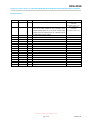
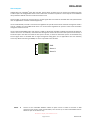
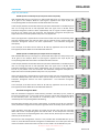
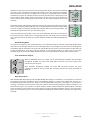
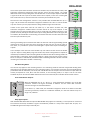
DDA-4010
Single 1 In, 8 Out / Dual 1 In, 4 Out 3G/HD/SD/ASI Reclocking/Non-Reclocking Distribution Amplifier
User Manual
IRT Electronics Pty Ltd | www.irtelectronics.com
Page 1 of 21
Revision 01
DDA-4010
Single 1 In, 8 Out / Dual 1 In, 4 Out 3G/HD/SD/ASI Reclocking/Non-Reclocking Distribution Amplifier
Revision History:
Revision
00
Date
03/01/2013
By
AL
01
03/06/2013
AL
Change Description
Original Issue.
DIP switch designators changed to SW1 and SW2,
links LK1 and LK2 added for rear assembly alarm
output NO/NC operation, front panel monitor BNC
outputs slew rate matches that of individual inputs
as opposed to current output.
Applicable to:
Issue 3 PCB units
fitted with
firmware version ≥ 2.1
Issue 4 PCB units
fitted with
firmware version ≥ 2.1
IRT Electronics Pty Ltd | www.irtelectronics.com
Page 2 of 21
Revision 01
DDA-4010
USER MANUAL
Table of Contents:
Section
Page
Revision History
Operational Safety
General Description
Technical Specifications
Configuration
DDA-4010 DIP Switch Settings
DDA-4010 Alarm Link Settings
Single 1 In, 8 Out Quick Set-up Guide
Dual 1 In, 4 Out Quick Set-up Guide
Installation
Signal Inputs & Outputs
Alarm Outputs
Front and Rear Layouts
Operation
Single 1 In, 8 Out Mode
ChAx8: Input A to all 8 Outputs
ChBx8: Input B to all 8 Outputs
Automatic Changeover Mode
Non-Reclocking Mode
Front Panel Monitor Outputs
Relay Bypass Option
Dual 1 In, 4 Out Mode
Input A to 4 Output A, and Input B to 4 x Output B
Automatic Changeover Mode
Non-Reclocking Mode
Front Panel Monitor Outputs
Relay Bypass Option
SNMP – What Is It?
DDA-4010 SNMP Functions
Maintenance & Storage
Warranty & Service
2
4
5
6
7
7
8
8
9
10
10
11
12
13
13
13
13
13
14
14
14
15
15
15
16
16
16
17
19
21
21
This instruction book applies to Issue 4 PCB units fitted with firmware version ≥ 2.1
IRT Electronics Pty Ltd | www.irtelectronics.com
Page 3 of 21
Revision 01
DDA-4010
OPERATIONAL SAFETY
WARNING
Operation of electronic equipment involves the use of voltages and currents that
may be dangerous to human life. Note that under certain conditions dangerous
potentials may exist in some circuits when power controls are in the OFF position.
Maintenance personnel should observe all safety regulations.
Do not make any adjustments inside equipment with power ON unless proper
precautions are observed. All internal adjustments should only be made by suitably
qualified personnel. All operational adjustments are available externally without
the need for removing covers or use of extender cards.
IRT Electronics Pty Ltd | www.irtelectronics.com
Page 4 of 21
Revision 01
DDA-4010
GENERAL DESCRIPTION
BLOCK DIAGRAM DDA-4010 SIGNAL PATH
SINGLE / DUAL MODE
DATA RATE
RECLOCK / NON-RECLOCK
I/P INVERT (x2)
AUTO CHANGEOVER
ALARM A
MON A
OUT 1A
OUT 2A
OUT 3A
IN A
EQUALISER
OUT 4A
RECLOCKER
IN B
OUT 4B
EQUALISER
OUT 3B
SNMP
OUT 2B
OUT 1B
Optional Relay Bypass on loss of power
In Dual 1 In, 4 Out mode:
IN 1 & IN 2 independently either 3G/HD/SD-SDI or ASI
MON B
ALARM B
The DDA-4010 serial digital data distribution amplifier provides the user with a single module to cover a wide range
of distribution and monitoring functions for 3G/HD/ SD-SDI or ASI signals.
Two quad output reclocking / non-reclocking distribution amplifiers are provided on the one card. On board switch
settings allow either of the inputs to feed all outputs to create a one in, eight out distribution amplifier.
Where non-reclocking is required, on-board switch settings select between reclocking and non-reclocking modes.
The DDA-4010 will automatically reclock to match the input at either 3G-SDI, HD-SDI, SD-SDI or ASI rates, or can be
fixed to operate at any one of these rates. Both sides of the DDA-4010 can be run independently allowing a mixture
of signal types to be used.
The DDA-4010 is also configurable for Automatic Changeover from one input to the other on loss of input signal
allowing for an input Main/Standby scenario.
Due to the nature of ASI signals being phase sensitive, signal inversion is also possible for situations where an
inverted ASI signal needs to be corrected.
Front panel LEDs indicate when input signals are present and whether the outputs are locked to the inputs.
An optional relay bypass rear assembly is available to switch the Inputs to one of their respective Outputs in the
event of a power failure.
Simple Network Management Protocol (SNMP) is available for remote setup and monitoring of input status and
alarm states when used in an IRT frame fitted with SNMP capability.
The DDA-4010 is designed to fit IRT’s 4000 series 3RU frame for use with IRT’s SNMP system as well as being
suitable with IRT’s 1000 series 1RU Eurocard frames and may be used alongside any other of IRT’s Eurocards.
Standard features:
• Switch selectable for 1 in, 8 out single distribution amplifier operation.
•
•
•
•
•
•
•
•
In-phase reclocked / non-reclocked outputs on each amplifier.
Selectable for either 3G/HD/SD-SDI or ASI applications.
Automatic output muting on no input.
Front panel monitoring outputs.
Front panel indicators provide monitoring of presence of inputs and lock status.
Automatic changeover to second input on loss of primary input (selectable).
Optional relay bypass on loss of power.
SNMP monitoring and control.
IRT Electronics Pty Ltd | www.irtelectronics.com
Page 5 of 21
Revision 01
DDA-4010
TECHNICAL SPECIFICATIONS
Data Inputs:
Number
Impedance
Type
Return loss
Equalisation Automatic
Data Outputs:
Number
Type
Level
Impedance
Return loss
8 (1 in, 8 out; or (2x) 1 in, 4 out), plus 2 front panel monitoring.
Reclocked or non-reclocked, switch selectable.
800 mV ± 10%.
75 Ω, BNC.
15dB 5 MHz to 1.485 GHz,
10dB from 1.485 GHz to 2.97 GHz1.
Performance:
Reclocking
Rise Time
3G/HD
SD
Intrinsic Jitter
Indicators:
DC
INPUT A
INPUT B
SD
Automatic or selectable for 3G-SDI, HD-SDI or SD-SDI / ASI operation.
< 135 ps at 2.97 Gb/s and 1.485 Gb/s;
> 0.4 ns and < 1.5 ns at 270 Mb/s.
< 0.3 UI at 2.97 Gb/s reclocked;
< 0.2 UI at 1.485 Gb/s reclocked;
< 0.1 UI at 270 Mb/s reclocked.
LED (green) for module power.
LED (green) when signal present on channel A input (LED flashes if present but not active5).
LED (green) when signal present on channel B input (LED flashes if present but not active5).
LED (green) x2 when SD-SDI or ASI signal present and locked to selected input on
either A or B outputs.
LED (green) x2 when HD-SDI signal present and locked to selected input on either A or
B outputs.
LED (green) x2 when 3G-SDI signal present and locked to selected input on either A or
B outputs.
HD
3G
Alarm Outputs:
Alarm A
A alarm switches to either open circuit or ground (link selectable) via MOSFET relays
on either loss of signal or incorrect signal rate on I/P A.
B alarm switches to either open circuit or ground (link selectable) via MOSFET relays
on either loss of signal or incorrect signal rate on I/P B.
Alarm B
Power requirement:
Voltage
Power consumption
Other:
Temperature
Mechanical
Finish
2
75 Ω, BNC.
3G-SDI, HD-SDI, SD-SDI or ASI (to SMPTE 424M, 292M and 259M-C standards; and
DVB-ASI standard).
15dB 5 MHz to 1.485 GHz,
10dB from 1.485 GHz to2.97 GHz1.
100 m at 3G-SDI rate with Belden 1694A2;
200 m at HD-SDI rate with Belden 16942,3, 120 m with Belden 82812,3;
400 m at SD-SDI/ASI rate with Belden 16943, 300 m with Belden 82813,4.
28 Vac CT (14-0-14) or ±16 Vdc.
< 6 VA.
Front panel
Rear assembly
0 - 50°C ambient.
Suitable for mounting in IRT 19" rack chassis with input, output and power
connections on the rear panel.
Grey background, black lettering & red IRT logo.
Detachable silk-screened PCB with direct mount connectors to Eurocard and external signals.
6 HP x 3 U x 220 mm IRT Eurocard.
Rear connector assembly with matching connector for alarm output.
ZDA-4010RL relay bypass rear assembly suitable for 3G-SDI1, HD-SDI and SD-SDI/ASI signals.
NOTE: 1
2
3
4
5
Return loss reduced by a couple of dB at 3G rate with optional bypass relay.
Reduces to ~ 50m with optional bypass relay rear assembly.
If two inputs are being inputted, cable equalisation is limited to that of the higher rate.
Reduces to ~ 70m when SW1-4 (I/P A), SW2-4 (I/P B) is ON.
When automatic change-over function has been set.
Dimensions
Standard
Optional
Due to our policy of continuing development, these specifications are subject to change without notice.
IRT Electronics Pty Ltd | www.irtelectronics.com
Page 6 of 21
Revision 01
DDA-4010
CONFIGURATION
The DDA-4010 may be configured as a Dual 1 In, 4 Out or a Single 1 In, 8 Out distribution amplifier either locally via
on board DIP switch settings, or remotely via SNMP.
To configure DDA-4010 via SNMP, DIP switch Sw2-7 must be set to ON.
DDA-4010 DIP Switch Settings:
Input A signal type (rate set)
Auto Detect (3G/HD/SD/ASI rates)
SD-SDI / ASI only
HD-SDI only
3G-SDI only
SW1-1
OFF
ON
OFF
ON
SW1-2
OFF
OFF
ON
ON
SW1-3
OFF Reclocking mode. DA behaves as a Reclocking DA.
ON Non-Reclocking mode (Reclocker bypassed). DA behaves as a Non-Reclocking DA.
SW1-4
OFF I/P A Normal cable equalisation.
ON I/P A Reduced cable equalisation to ~ 70m for shorter cable for use in a noisy environment.
SW1-5
OFF Single 1 In, 8 Out DA mode.
ON Dual 1 In, 4 Out DA mode (IN A → ‘A’ Outputs (OUT 1A, OUT 2A, OUT 3A & OUT 4A);
(IN B → ‘B’ Outputs (OUT 1B, OUT 2B, OUT 3B & OUT 4B).
SW1-6
OFF Non-invert I/P A (Default position).
6
ON Invert I/P A.
SW1-7
OFF Auto Changeover Function disabled.
ON Auto Changeover Function enabled.
SW1-8
Not Used.
Input B signal type (rate set)
Auto Detect (3G/HD/SD/ASI rates)
SD-SDI / ASI only
HD-SDI only
3G-SDI only
SW2-1
OFF
ON
OFF
ON
SW2-2
OFF
OFF
ON
ON
SW2-3
OFF I/P B Reclocking mode. DA behaves as a Reclocking DA.
ON I/P B Non-Reclocking mode (Reclocker bypassed). DA behaves as a Non-Reclocking DA.
SW2-4
OFF I/P B Normal cable equalisation.
ON I/P B Reduced cable equalisation to ~ 70m for shorter cable for use in a noisy environment.
SW2-5
OFF I/P A primary I/P of single 1 in, 8 out DA (IN A → All 8 Outputs).
ON I/P B primary I/P of single 1 in, 8 out DA (IN B → All 8 Outputs). Not applicable to Dual mode.
SW2-6
OFF Non-invert I/P B (Default position).
6
ON Invert I/P B.
SW2-7
OFF DIP Switch control. Settings as per DIP switch settings.
ON SNMP control. Settings as per SNMP settings.
SW2-8
OFF Enable major and minor SNMP alarms to the frame Agent (CDM card) .
7
ON Disable major and minor SNMP alarms to the frame Agent (CDM card) .
NOTE:
6
Due to the nature of ASI signals being phase sensitive, signal inversion is possible with this
switch for situations where an inverted ASI signal needs to be corrected.
7
When using TRAPS via SNMP, depending on how system is set up, in order to avoid double
reporting of alarms via the DDA-4010 card itself and the CDM card (SNMP Agent) of the
frame, major and minor SNMP alarms that are reported to the CDM card of the frame can be
disabled.
7
IRT Electronics Pty Ltd | www.irtelectronics.com
Page 7 of 21
Revision 01
DDA-4010
DDA-4010 Alarm Link Settings:
8
1-2 A alarm switches to open circuit on either loss of signal or incorrect signal rate on A I/P.
2-3 A alarm switches to closed circuit on either loss of signal or incorrect signal rate on A I/P.
8
1-2 B alarm switches to open circuit on either loss of signal or incorrect signal rate on B I/P.
2-3 B alarm switches to open circuit on either loss of signal or incorrect signal rate on B I/P.
LK 1
LK 2
NOTE:
8
Alarm O/P non-active with link not plugged into either 1-2 or 2-3 (permanently open circuited).
Single 1 In, 8 Out Quick Set-up Guide:
ChAx8 - Input A to all 8 Outputs (4 x Output A and 4 x Output B) Reclocking DA:
Sw1-5 = OFF
Sw2-5 = OFF
(Single 1 In, 8 Out DA mode).
(Input A primary input).
Note that it is also possible to set Input B to all 8 Outputs, if desired.
ChBx8 - Input B to all 8 Outputs (4 x Output A and 4 x Output B):
Sw1-5 = OFF
Sw2-5 = ON
(Single 1 In, 8 Out DA mode).
(Input B primary input).
Data Rate:
For automatic detection of signal type so that DDA-4010 will pass 3G-SDI, HD-SDI and SD-SDI/ASI
automatically:
Sw1-1 = OFF.
Sw1-2 = OFF.
For 3G-SDI only, HD-SDI only or SD-SDI/ASI only, see Sw1-1 and SW1-2 settings on page 8.
Note that Sw2-1 and Sw2-2 have no effect when being run in the Single 1 In, 8 Out mode.
Reclocking DA Mode:
Sw1-3 = OFF (Input reclocked. DA behaves as a reclocking DA).
Sw2-3 = Not Applicable.
Non-Reclocking DA Mode:
Sw1-3 = ON
(Input non-reclocked. DA behaves as a non-reclocking DA).
Sw2-3 = Not Applicable.
Reduced equalisation in a noisy environment:
Sw1-4 = ON
Sw2-4 = ON
(Input A cable equalisation reduced).
(Input B cable equalisation reduced. Relevant only if Automatic Changeover
enabled).
Automatic Changeover Mode:
On loss of primary input, secondary input will switch to all 8 outputs. See Operation section for complete
description.
Sw1-7 = OFF
Sw1-7 = ON
(Auto Changeover disabled).
(Auto Changeover enabled).
IRT Electronics Pty Ltd | www.irtelectronics.com
Page 8 of 21
Revision 01
DDA-4010
Dual 1 In, 4 Out Quick Set-up Guide:
Note that in Dual 1 In, 4 Out mode, each half of the DDA-4010 behaves as an independent DA, which means that
each input can be set with different (or the same) data rate and Reclock/Non-Reclock mode settings.
Input A to 4 x Output A, and Input B to 4 x Output B:
Sw1-5 = ON
(Dual 1 In, 4 Out mode).
Sw2-5 = Not Applicable.
Reclocking Mode:
Sw1-3 = OFF
Sw2-3 = OFF
(Input A reclocked. A input behaves as a reclocking DA).
(Input B reclocked. B input behaves as a reclocking DA).
Non-Reclocking Mode:
Sw1-3 = ON
Sw2-3 = ON
(Input A non-reclocked. A input behaves as a non-reclocking DA).
(Input B non-reclocked. B input behaves as a non-reclocking DA).
Reduced equalisation in a noisy environment:
Sw1-4 = ON
Sw2-4 = ON
(Input A cable equalisation reduced).
(Input B cable equalisation reduced).
Automatic Changeover Mode:
On loss of one input, other input will switch to all 8 outputs. See Operation section for complete description.
Sw1-7 = OFF
Sw1-7 = ON
(Auto Changeover disabled).
(Auto Changeover enabled).
IRT Electronics Pty Ltd | www.irtelectronics.com
Page 9 of 21
Revision 01
DDA-4010
INSTALLATION
Pre-installation:
Handling:
This equipment may contain or be connected to static sensitive devices and proper static free handling precautions
should be observed.
Where individual circuit cards are stored, they should be placed in antistatic bags. Proper antistatic procedures
should be followed when inserting or removing cards from these bags.
Power:
AC mains supply:
Ensure that operating voltage of unit and local supply voltage match and that correct rating
fuse is installed for local supply.
DC supply:
Ensure that the correct polarity is observed and that DC supply voltage is maintained within
the operating range specified.
Earthing:
The earth path is dependent on the type of frame selected. In every case particular care should be taken to ensure
that the frame is connected to earth for safety reasons. See frame manual for details.
Signal earth: For safety reasons a connection is made between signal earth and chassis earth.
No attempt should be made to break this connection.
Installation in frame or chassis:
See details in separate manual for selected frame type.
Signal Inputs & Outputs:
For use with supplied standard rear assembly (ZDA-4010) or optional relay bypass rear assembly (ZDA-4010RL).
The DDA-4010 can be configured as a single 1 IN, 8 OUT distribution amplifier, or as a dual 1 IN, 4 OUT distribution
amplifiers as described in the Configuration section of this handbook. If set up for a 1 IN, 8 OUT distribution
amplifier, either input can be configured as the primary input. The other input is not used except when the
automatic changeover function is enabled, in which case this becomes the secondary input. See the Operation
section of this manual for a complete description.
Inputs, Outputs and front panel monitoring ports are 75 Ω BNC type for connection with high quality 75 Ω coaxial
cable. Inputs are self-terminating.
An optional relay bypass rear assembly (ZDA-4010RL) is available where the inputs are outputted to one of the
respective outputs (OUT 1A for Input A, and OUT 1B for Input B) on loss of power or removal of the card from the
rear assembly itself. The bypass relay is suitable for all specified signals up to 3G-SDI. Note however that the cable
equalisation at the 3G/HD-SDI rates and the return loss at the 3G-SDI rates are reduced through these relays. Note
also that if operating in the 1x8 mode, if anything is connected to the secondary input this too will be switched to
one of the outputs on loss of power or removal of card.
IRT Electronics Pty Ltd | www.irtelectronics.com
Page 10 of 21
Revision 01
DDA-4010
Alarm Outputs:
9
Independent, link selectable (links LK1 and LK2), alarms switch to Open Circuit or Ground are available for both
A and B inputs. See Configuration section of this manual for relevant link positions. Alarm outputs are via MOSFET
relays limited to 120mA maximum continuous load current.
Alarms trigger on either loss of signal input or if input signal does not match the selected data rate (selected data
rate not applicable if reclocker has been bypassed).
If in the ChAx8 mode, alarm B is non-functional regardless of input B’s status unless automatic changeover mode is
also set. Likewise if in the ChBx8 mode alarm A is non-functional regardless of input A’s status unless automatic
changeover mode is also set.
If in the dual ChAx4-ChBx4 mode, both alarms A and B are functional regardless of whether Automatic Changeover
mode is also set or not. However, if the Automatic Changeover mode is set and one of the inputs were to be lost, if
the other input’s rate does not match the lost input’s set rate, an alarm for that other input is not activated. Only
the lost signal alarm is activated with no signal changeover taking place. This is applicable to the rear assembly
alarm only. When monitoring via SNMP, an alarm is reported in this situation.
NOTE:
9
1
GND.
2
Alarm A.
3
Alarm B.
Alarms are link selectable between switch to Open Circuit or switch to Ground on PCB
revisions ≥ Issue 4 only. Earlier revision PCB’s, such as Issue 3, are not link selectable and are
switch to open circuit alarms only.
IRT Electronics Pty Ltd | www.irtelectronics.com
Page 11 of 21
Revision 01
DDA-4010
Front & rear panel connector diagrams
ZDA-4010
Standard
Rear Assembly
ZDA-4010RL
3G/HD/SD/ASI
Relay Bypass
Rear Assembly
IRT Electronics Pty Ltd | www.irtelectronics.com
Page 12 of 21
Revision 01
DDA-4010
OPERATION
Single 1 In, 8 Out Mode:
ChAx8: Input A to all 8 Outputs (4 x Output A and 4 x Output B):
With the DDA-4010 set-up in the single 1 In, 8 Out mode with input ‘A’ as the primary input,
‘IN A’ goes to all 8 outputs. When an input signal is applied to the input A port, the
corresponding INPUT A and both data rate A & B LEDs will illuminate.
A
B
A
B
A
B
A
B
A
B
A
B
INPUT
SD
In this example, the data rate has either been set up for either ‘Auto Detect’ or ‘HD-SDI only’ data
rate and is being fed with an HD equivalent data rate signal such as HD-SDI. Unless
Automatic Changeover mode has been implemented, even if a signal has been applied to
the ‘IN B’ port, INPUT B will not illuminate. See Automatic Changeover description for
explanation of how secondary INPUT LED (in this case, B) behaves.
If the input signal that is applied does not match the set data rate, the corresponding input
and both detected data rate LEDs will flash and the outputs will be muted (unless the
Automatic Changeover function has been implemented - see Automatic Changeover
description).
HD
3G
INPUT
SD
HD
In this example, if the data rate has been set for HD only application and an SD rate has
been applied, both the INPUT A and SD A & B LEDs will flash.
3G
ChBx8: Input B to all 8 Outputs (4 x Output A and 4 x Output B):
With the DDA-4010 set-up in the single 1 In, 8 Out mode with input ‘B’ as the primary input,
‘IN B’ goes to all 8 outputs. When an input signal is applied to the input B port, the
corresponding INPUT B and both data rate A & B LEDs will illuminate.
INPUT
SD
In this example, the data rate has either been set up for either ‘Auto Detect’ or ‘HD-SDI only’ data
rate and is being fed with an HD equivalent data rate signal such as HD-SDI. Unless
Automatic Changeover mode has been implemented, even if a signal has been applied to
the ‘IN A’ port, INPUT A will not illuminate. See Automatic Changeover description for
explanation of how secondary INPUT LED (in this case, A) behaves.
If the input signal that is applied does not match the set data rate, the corresponding input
and both detected data rate LEDs will flash and the outputs will be muted (unless the
Automatic Changeover function has been implemented - see Automatic Changeover
description).
HD
3G
INPUT
SD
HD
In this example, if the data rate has been set for HD only application and an SD rate has
been applied, both the INPUT B and SD A & B LEDs will flash.
3G
Automatic Changeover Mode:
With the Automatic Changeover mode enabled, provided a secondary input is present at
the correct set data rate, on loss of the primary input the outputs will automatically switch
to the secondary input. The presence of a secondary input, in this example ‘IN B’, is
indicated by the corresponding INPUT LED flashing.
INPUT
SD
HD
Note that when the data rate is set for ‘Auto Detect’, or the DA is set-up for non-reclocking
mode, Automatic Changeover will take place regardless of the secondary input’s data rate.
If the secondary input data rate does not match the set data rate, both the secondary
INPUT LED and its corresponding data rate LED will flash. In this example the secondary
input is ‘IN B’ and its corresponding data rate is at the SD rate, whilst input A’s data rate is
obviously set for the HD rate.
3G
INPUT
SD
HD
Note that this LED configuration scenario is also possible with the DDA-4010 set up as a
dual 1 IN, 4 Out DA with Automatic Changeover enabled where one of the inputs does not
match its sets data rate but the other one does. In this case B is set for HD-SDI only rate.
3G
IRT Electronics Pty Ltd | www.irtelectronics.com
Page 13 of 21
Revision 01
DDA-4010
Likewise, if the primary input source was to change its data rate to not match what the data
rate was set for, provided the secondary was at the correct rate, Automatic Changeover
would take place and the primary INPUT LED and both its corresponding data rate LEDs
would flash. This gives an indication of which input was actually set up as the primary input.
In this example ‘IN B’ would actually represent the primary input and ‘IN A’ would take
control with B’s data rate being set up for the HD rate, but actually being fed with an SD
data rate.
If both the primary and secondary input data rates do not match the set data rate, both the
primary and secondary INPUT LEDs and their corresponding data rate LEDs will flash. Being
set up as a single 1 In, 8 Out DA, the both data rate LEDs of the primary input will flash. This
shows which input has been set up as the primary input.
A
B
A
B
INPUT
SD
HD
3G
INPUT
SD
HD
In this example the primary input is ‘IN A’ and its corresponding data rate is at the 3G rate.
The secondary input is ‘IN B’ and its corresponding data rate is at the SD rate. The set data
rate is obviously set for HD-SDI only as neither INPUT A (3G-SDI) nor INPUT B (SD-SDI) take
control.
3G
Non-Reclocking Mode:
The rate set only applies to the reclocking mode. In non-reclocking mode the reclocker is bypassed allowing other
data rates to pass through. Whilst in the non-reclocking mode, if an input signal is present, the corresponding front
panel INPUT LED will illuminate, but the 3G, HD and SD LEDs will not except in the case where the input data rate
actually corresponds to a 3G, HD or SD rate. Likewise, in the reclocking mode, if an input is not at one of the
standard 3G, HD or SD rates the INPUT LED will flash and none of the 3G, HD or SD LEDs will illuminate or flash.
Front Panel Monitor Outputs:
CH.A
CH.B
With the DDA-4010 set up as a Single 1 In, 8 Out Distribution Amplifier with Automatic
Changeover disabled, the ‘CH.A’ and ‘CH.B’ BNC connectors on the front panel both
monitor the primary input.
With Automatic Changeover enabled, the ‘CH.A’ BNC connector monitors the signal
connected to INPUT A and the ‘CH.B’ BNC connector monitors the signal connected to
INPUT B.
Relay Bypass Option:
With the DDA-4010 fitted with the optional ZDA-4010RL relay bypass rear assembly, on loss of power or removal of
the card from the frame, the INPUT A signal is automatically routed via a relay to the output ‘OUT 1A’ port, as is
the INPUT B signal to the output ‘OUT 1B’ port. Thus if the DDA-4010 is being run in the single 1 In, 8 Out mode, if
anything is connected to the secondary input port, whether the Automatic Changeover mode is enabled or not,
the secondary input is also routed to one of the outputs. Caution should therefore be observed when connecting
to the secondary input to connect the correct signal if using the Automatic Changeover mode, or not connecting a
signal to the secondary input at all with the Automatic Changeover disabled, when using the relay bypass rear
assembly.
IRT Electronics Pty Ltd | www.irtelectronics.com
Page 14 of 21
Revision 01
DDA-4010
Dual 1 In, 4 Out Mode:
Input A to 4 x Output A, and Input B to 4 x Output B:
With the DDA-4010 set-up in the dual 1 In, 4 Out mode, the DDA-4010 is essentially two independent distribution
amplifiers each with a single input and 4 outputs:
Input signal ‘IN A’ goes to outputs ‘OUT 1A’, ‘OUT 2A’, ‘OUT 3A’ and ‘OUT 4A’; and
Input signal ‘IN B’ goes to outputs ‘OUT 1B’, ‘OUT 2B’, ‘OUT 3B’ and ‘OUT 4B’.
Each of the input’s data rates can be set independently from each other, either ‘Auto Detect’ for automatic
detection of 3G/HD/SD-SDI or ASI rates, ‘3G-SDI only’, ‘HD-SDI only’ or ‘SD-SDI/ASI only’ rates. Either side can also
be individually configured as a reclocking or non-reclocking distribution amplifier.
When an input signal is applied, the corresponding INPUT and data rate LEDs will illuminate.
In this example, INPUT A has been set up for either ‘Auto Detect’ or ‘SD-SDI/ASI only’ data rate
and is being fed with a 270Mb/s data rate signal such as SD-SDI or ASI, and INPUT B has
either been set up for either ‘Auto Detect’ or ‘HD-SDI only’ data rate and is being fed with
an HD equivalent data rate signal such as HD-SDI.
If an input signal that is applied does not match the set data rate, the corresponding input
and detected data rate LEDs will flash and the corresponding outputs will be muted (unless
the Automatic Changeover function has been implemented - see Automatic Changeover
description).
A
B
A
B
A
B
A
B
A
B
INPUT
SD
HD
3G
INPUT
SD
HD
In this example, if Input A has been set for 3G or HD only application and an SD rate has
been applied, both the INPUT A and SD A LEDs will flash.
3G
Automatic Changeover Mode:
With the Automatic Changeover mode enabled, provided the other DA input is present at
the correct set data rate of the current DA, on loss of either input the outputs will
automatically switch to the other DA’s outputs.
INPUT
SD
In this example, both independent DA’s are operating in either Auto Detect, HD only or
reclocker bypassed modes. INPUT A feeds A outputs and INPUT B feeds B outputs.
HD
3G
On loss of INPUT A, INPUT B takes control of A outputs as well as its own B outputs.
INPUT
SD
HD
3G
On loss of INPUT A, if A was set for SD-SDI/ASI only rate and INPUT B was being fed with an
HD-SDI signal, INPUT B would not take control of A outputs. A outputs would be muted. The
HD data LED of A would flash to indicate that B’s input, which is currently an HD signal, is
not at A’s set data rate.
INPUT
SD
HD
Note that when the data rate is set for ‘Auto Detect’, or the DA is set-up for non-reclocking
mode, Automatic Changeover will take place regardless of the second input’s data rate.
3G
IRT Electronics Pty Ltd | www.irtelectronics.com
Page 15 of 21
Revision 01
DDA-4010
If one of the input’s data rate does not match its set data rate, but the other one does, with
Automatic Changeover enabled the other will take control of both outputs. The invalid
INPUT LED and its corresponding data rate LED will flash. In this example input B is fed with
a signal at the SD rate. Input A has taken control of B’s outputs, in this case A is being fed
with an HD rate source, hence B’s data rate is obviously set for HD-SDI only rate.
A
B
A
B
A
B
INPUT
SD
HD
3G
Note that this LED configuration scenario is also possible with the DDA-4010 set up as a
single 1 IN, 8 Out DA with Automatic Changeover enabled In this case A is set for HD-SDI
only rate and is the primary input whilst B is being fed with a signal at the SD rate.
If both of the inputs data rates do not match its, or the other’s set data rate, with
Automatic Changeover enabled neither will take control of any of the outputs. In this
example input A is being fed with either an SD or an HD data rate, likewise input B. It is not
possible to tell by looking at the LEDs which input is being fed with the SD or HD signal, but
as all INPUT, SD and HD LEDs are all flashing it is obvious that both A and B’s data rates have
been set up for 3G-SDI only rate.
If the signal feeding input A matches that of B’s set data rate and the signal feeding input B
matches that of A’s set data rate, where A and B’s set data rate are not set the same as
each other, it is possible for input A to be feeding B’s outputs whilst input B is feeding A’s
outputs.
INPUT
SD
HD
3G
INPUT
SD
HD
In this example A has been set at the HD-SDI only rate and B has been set for the SD-SDI
only rate. Input A is being fed by a signal at the SD rate, which is being fed to B’s outputs as
indicated by the INPUT A LED not flashing whilst A’s SD data rate LED is flashing and B’s SD
data rate LED is not flashing. Input B is being fed by a signal at the HD rate, which is being
fed to A’s outputs as indicated by the INPUT B LED not flashing whilst B’s HD data rate LED
is flashing and A’s HD data rate LED is not flashing.
3G
Non-Reclocking Mode:
The rate set only applies to the reclocking mode. In non-reclocking mode the reclocker is bypassed allowing other
data rates to pass through. Whilst in the non-reclocking mode, if an input signal is present, the corresponding front
panel INPUT LED will illuminate, but the 3G, HD and SD LEDs will not except in the case where the input data rate
actually corresponds to a 3G, HD or SD rate. Likewise, in the reclocking mode, if an input is not at one of the
standard 3G, HD or SD rates the INPUT LED will flash and none of the 3G, HD or SD LEDs will illuminate or flash.
Front Panel Monitor Outputs:
CH.A
CH.B
With the DDA-4010 set up as a Dual 1 In, 4 Out Distribution Amplifier, the ‘CH.A’ BNC
connector monitors the signal connected to INPUT A and the ‘CH.B’ BNC connector
monitors the signal connected to INPUT B.
In the Dual 1 In, 4 Out mode, the Automatic Changeover mode has no effect on the BNC
monitoring connectors, whether it is enabled or disabled, as in the case of when set up as a
Single 1 In, 8 Out DA.
Relay Bypass Option:
With the DDA-4010 fitted with the optional ZDA-4010RL relay bypass rear assembly, on loss of power or removal of
the card from the frame, the INPUT A signal is automatically routed via a relay to the output ‘OUT 1A’ port, as is
the INPUT B signal to the output ‘OUT 1B’ port.
IRT Electronics Pty Ltd | www.irtelectronics.com
Page 16 of 21
Revision 01
DDA-4010
SNMP
What Is It?
SNMP stands for Simple Network Management Protocol. It is an application layer protocol for managing IP
(Internet Protocol) based systems. SNMP enables system administrators to manage system performance, and to
find and solve system problems. SNMP runs over UDP (User Datagram Protocol), which in turn runs over IP.
Three types of SNMP exist: SNMP version 1 (SNMPv1), SNMP version 2 (SNMPv2) and SNMP version 3 (SNMPv3). It
is not the intention here to discuss the differences between various versions, only to bring attention to the fact
that IRT Electronics modules, fitted with SNMP capability, use SNMPv1.
An SNMP managed network consists of three key components: Network Management Systems (NMS), agents, and
managed devices.
An NMS is the console through which the network administrator performs network management functions, such
as monitoring status (e.g. alarm states) and remote controlling, of a set of managed devices. One or more NMS’s
must exist on any managed network. Generally the NMS is a computer running third party SNMP control software.
There are a number of third party SNMP software applications currently available on the market.
An NMS polls, or communicates with, an agent. An agent is a network management software module that resides
in a managed device. An agent has local knowledge of management information and translates that information
into a form compatible with SNMP. The agent, therefore, acts as an interface between the NMS and the managed
devices. The NMS sends a request message, and control commands for the managed devices, to the agent, which
in turn sends a response message, containing information about the managed devices, back to the NMS.
A managed device contains an SNMP agent and resides on a managed network. Managed devices collect and store
management information and make this information available to NMS’s using SNMP.
Managed device agent variables are organised in a tree structure known as a Management Information Base
(MIB). Within the MIB are parameters pertaining to the managed device. An Object Identifier (OID) number within
the MIB defines the managed device type. This is a unique number specific to the model of managed device. Other
information relating to the device is also stored, information such as alarm states, controllable settings, etc. The
MIB tree is organised in such a way that there will be no two MIB files with conflicting placements.
Normally an NMS polls an agent for information relating to the MIB in a managed device to be sent back to the
NMS. When certain conditions are met within the MIB, such as major alarm conditions, for example, the agent
automatically sends what is known as a trap to the NMS without any prompting from the NMS. This allows
automatic notification of a predetermined event.
SNMP Block Diagram
NMS
IP
Network
NMS
SNMP Agent
Protocol Engine
MIB
SNMP Agent
SNMP Agent
Protocol Engine
MIB
SNMP Agent
SNMP Agent
Protocol Engine
MIB
SNMP Agent
IRT Electronics Pty Ltd | www.irtelectronics.com
Page 17 of 21
Revision 01
DDA-4010
SNMP with IRT Products:
IRT Electronics currently employs SNMPv1 with its SNMP capable frames. The frame acts as an agent when fitted
with a CDM-xxxx module. This module has its own designated slot next to the power supply so as to not affect the
number of modules that the frame will take. Communication between the NMS, the frame and its loaded modules
are via this CDM-xxxx module. Note that the NMS software is third party and not supplied by IRT Electronics.
Ethernet connection for SNMP operation is via an RJ45 connector on the rear of the frame, below the mains inlet.
Ethernet rate runs at either 10 baseT or 100 baseT.
Frame parameters, such as Name, Address and Location, are set via an RS232 interface, a D9 connector on the rear
of the frame below the mains inlet. A software terminal emulator, such as Tera Term or HyperTerminal, is used for
setting and reading the parameters of the frame.
IRT modules that are SNMP compatible may need an optional plug-in SNMP module with a program relevant to the
module that it is plugged into. Depending on the module, besides the module identification, parameters such as
alarm states, inputs and controls etc. are communicated to the CDM-xxxx agent via a data bus on the rear of the
frame. Thus the CDM-xxxx collects information on what is loaded within the frame, what positions they occupy,
and their current status for communication to the NMS when the NMS sends a request for information.
In the event of a major alarm from any of the SNMP compatible modules, or power supplies, a trap is automatically
sent by the CDM-xxxx agent to the NMS without any prompting by the NMS. This alerts the operator to any fault
conditions that may exist that need immediate attention.
110/240 V 50/60 Hz
0.7 A (max.)
FRU-4000
FRAME
FUSES
220/240 Vac
500 mA S.B.
110/120 Vac
1A S.B.
RS232
Alarm
Ethernet
+
48Vdc
AS3260 approval no.: CS6346N
Ass. no.: 804692
IRT SNMP Connections
NMS
Ethernet Cable
IP
Network
IRT modules fitted
with SMU-4000
CDM-xxxx
PSU’s
IRT SNMP Frame
Ethernet Cable
IRT modules fitted
with SMU-4000
CDM-xxxx
PSU’s
IRT SNMP Frame
Ethernet Cable
IRT SNMP Setup
IRT Electronics Pty Ltd | www.irtelectronics.com
Page 18 of 21
Revision 01
DDA-4010
DDA-4010 SNMP Functions:
With the DDA-4010 installed in an IRT frame with SNMP capability, the unit can be interrogated by an SNMP
Network Management System (NMS):
sysDescr
- A description of the unit:
DDA-4010 1:8 or Dual 1:4 3G/HD/SD Distribution Amplifier.
sysUpTime
- A indication of how long the unit has been running since its last power on or reset in
Days, Hours, Minutes and Seconds.
sysName
- A 16 character writable system name. Default set name: DDA-4010.
alarms
- An indication of the current state of the Channel Status alarms:
(1) noAlarm: No alarms present.
(2) urgent-A: Input A is absent or does not match the set data rate.
(3) urgent-B: Input B is absent or does not match the set data rate.
(4) urgent-AB: Both input A & B are absent or do not match the set data rates.
(5) urgentA-nonUrgB: Primary input A and secondary input B are absent or do not
match the set data rate when in ChAx8 mode with automatic changeover enabled.
(6) urgentB-nonUrgA: Primary input B and secondary input A are absent or do not
match the set data rate when in ChBx8 mode with automatic changeover enabled.
(7) nonUrgent-A: Secondary input A is absent or does not match the set data rate
when in ChBx8 mode with automatic changeover enabled.
(8) nonUrgent-B: Secondary input B is absent or does not match the set data rate
when in ChAx8 mode with automatic changeover enabled.
ctrlMode
- The current configuration setting’s source as determined by DIP switch SW2-7 position:
(1) remoteSNMP: Configuration set remotely via SNMP (Sw2-7 = ON).
(2) pcbSwitches: Configuration set locally via on-board DIP switches (Sw2-7 = OFF).
distMode
- The current distribution mode setting as a single 1x8, or dual 1x4 distribution amplifier:
(1) chAx4-chBx4: Dual 1x4 DA. IN A → OUT 1A to OUT 4A; IN B → OUT 1B to OUT 4B.
(2) chAx8: Single 1x8 DA, IN A primary input. IN A → OUT 1A to OUT 4A & OUT 1B to OUT 4B.
(3) chBx8: Single 1x8 DA, IN B primary input. IN B → OUT 1B to OUT 4B & OUT 1A to OUT 4A.
autoChangeOver
- Enable or Disable Automatic Changeover to switch outputs from primary to secondary
input on loss of valid primary input (if secondary input is both present and valid):
(1) disabled: Automatic Changeover mode disabled.
(2) enabled: Automatic Changeover mode enabled.
- Information and control of the inputs in table form.
- Information and control of the separate individual inputs.
channelDesignator - An indication of the channel designator:
(1) chA: Channel designator A (IN A).
(2) chB: Channel designator B (IN B).
channelTable
channelEntry
inputStatus
- An indication of the input signal rate:
(1) unknownPresent: Input signal rate is not one of the 3G/HD/SD-SDI/ASI rates, or
10
is not being detected by the on-board reclocker .
(2) sdiSD-ASI Present: Input signal is either an SD-SDI or ASI signal, or at 270 Mb/s rate.
(3) sdiHD Present: Input signal is either an HD-SDI signal, or at 1.485 Gb/s rate.
(4) sdi3G Present: Input signal is either an 3G-SDI signal, or at 2.97 Gb/s rate.
(5) notPresent: no signal is present at the input.
outputStatus
- An indication of which input is feeding the outputs:
(1) inputA: Input A is feeding the outputs.
(2) inputB: Input B is feeding the outputs.
(3) muted: Outputs are muted. No input signal is feeding the outputs.
NOTE: 10
Whilst in either the chAx8 or chBx8 modes, with ‘autoChangeOver’ mode disabled, if a signal
is applied to the secondary input, SNMP ‘inputStatus’ is reported as ‘unknownPresent’. This is
because the secondary on-board reclocker chip is being used by the primary input to drive the
second front panel BNC monitor port. The correct rate is reported via SNMP ‘inputStatus’
when the ‘autoChangeOver’ mode is enabled as the secondary on-board reclocker chip is now
being used by the secondary input to drive its own relevant front panel BNC monitor port.
IRT Electronics Pty Ltd | www.irtelectronics.com
Page 19 of 21
Revision 01
DDA-4010
dataRateSet
- Control of the input data rate setting:
(1) autoDetect: Reclocker automatically set to incoming 3G-SDI, HD-SDI or SD-SDI/ASI
rates.
(2) sdiSD-ASI: Reclocker set to SD-SDI/ASI (270 Mb/s) rate only.
(3) sdiHD: Reclocker set to HD-SDI (1.485 Gb/s) rate only.
(4) sdi3G: Reclocker set to 3G-SDI (2.97 Gb/s) rate only.
(5) na: Data rate setting not applicable (secondary input of single 1x8 mode only). If
the user sets this parameter to ‘na’ the ‘dataRateSet’ will default to ‘autoDetect’
rate.
reclocker
- Enable or Bypass the reclocker for use as a reclocking or non-reclocking DA:
(1) enabled: Reclocker enabled. DA is set for a reclocking DA for 3G/HD/SD-SDI/ASI
rates only.
(2) bypassed: Reclocker is bypassed. DA is set for a non-reclocking DA. Other rates
other than 3G/HD/SD-SDI/ASI can also pass through regardless of what the
‘dataRateSet’ is set for.
(3) na: Reclocker enable/bypass option is not applicable to the secondary input of a
single 1x8 DA mode. If the user sets this parameter to ‘na’ the ‘reclocker’ will
default to the ‘enabled’ setting.
alias
- A 16 character maximum Alias (name) for the channel can be read and set.
inputStatusTrapEn -
11
Enable or Disable Traps to be sent when the input status condition changes :
(1) disabled: Input Status Trap not disabled.
(2) enabled: Input Status Trap enabled.
firmwareVer
- An indication of the firmware version of the microcontroller in the format ‘x.y’, where
x is the major revision number and y the minor.
reset
- Unit reset control:
(1) normal: when queried reset control returns a ‘normal’ state.
(2) reset: system reset causes ‘sysUpTime’ counter to reset.
NOTE: 11
With the ‘autoChangeOver’ mode disabled, change of state to the secondary input does not
cause an SNMP TRAP to be sent regardless of whether its ‘inputStatusTrapEn’ setting is
enabled or disabled. With the ‘autoChangeOver’ mode enabled, the secondary input is able to
generate TRAP’s if it is so enabled. ‘autoChangeOver’ mode has no affect on the primary
input’s TRAP generation capability.
IRT Electronics Pty Ltd | www.irtelectronics.com
Page 20 of 21
Revision 01
DDA-4010
MAINTENANCE & STORAGE
Maintenance:
No regular maintenance is required.
Care however should be taken to ensure that all connectors are kept clean and free from contamination of any
kind. This is especially important in fibre optic equipment where cleanliness of optical connections is critical to
performance.
Storage:
If the equipment is not to be used for an extended period, it is recommended the whole unit be placed in a sealed
plastic bag to prevent dust contamination. In areas of high humidity a suitably sized bag of silica gel should be
included to deter corrosion.
Where individual circuit cards are stored, they should be placed in antistatic bags. Proper antistatic procedures
should be followed when inserting or removing cards from these bags.
WARRANTY & SERVICE
Equipment is covered by a limited warranty period of three years from date of first delivery unless contrary
conditions apply under a particular contract of supply. For situations when “No Fault Found” for repairs, a
minimum charge of 1 hour’s labour, at IRT’s current labour charge rate, will apply, whether the equipment is
within the warranty period or not.
Equipment warranty is limited to faults attributable to defects in original design or manufacture. Warranty on
components shall be extended by IRT only to the extent obtainable from the component supplier.
Equipment return:
Before arranging service, ensure that the fault is in the unit to be serviced and not in associated equipment. If
possible, confirm this by substitution.
Before returning equipment contact should be made with IRT or your local agent to determine whether the
equipment can be serviced in the field or should be returned for repair.
The equipment should be properly packed for return observing antistatic procedures.
The following information should accompany the unit to be returned:
1.
2.
3.
4.
5.
6.
7.
A fault report should be included indicating the nature of the fault
The operating conditions under which the fault initially occurred.
Any additional information, which may be of assistance in fault location and remedy.
A contact name and telephone and fax numbers.
Details of payment method for items not covered by warranty.
Full return address.
For situations when “No Fault Found” for repairs, a minimum charge of 1 hour’s labour will apply,
whether the equipment is within the warranty period or not. Contact IRT for current hourly rate.
Please note that all freight charges are the responsibility of the customer.
The equipment should be returned to the agent who originally supplied the equipment or, where this is not
possible, to IRT directly. Details of IRT’s direct address can be found at IRT Electronics’ website.
Web address: www.irtelectronics.com
Email: [email protected]
IRT Electronics Pty Ltd | www.irtelectronics.com
Page 21 of 21
Revision 01