1
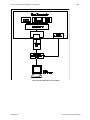
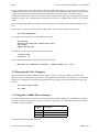
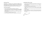
PCCtest 550/560 Serial Debugger User’s Manual M200023-03 October 2002 Preliminary Sycard Technology 1180-F Miraloma Way Sunnyvale, CA 94085 (408) 749-0130 (408) 749-1323 FAX http://www.sycard.com PCCtest 550/560 Serial Debugger User’s Manual Page 1 1.0 Introduction The PCCtest 550/560 CardBus socket tester is an enhanced version of the PCCtest model 460. The on-board RS-232 serial interface allows the user to perform various monitor and control functions on the CardBus, 16-bit and Zoomed Video (ZV) interface. The PCCtest 550/560 is fully compatible with the PCCtest 460 and may be used to test the CardBus, 16-bit and ZV interface. 1.1 Features The PCCtest 550/560 is fully compatible with the PCCtest 460. In addition the PCCtest 550/560 has a serial debug port that allows the user to debug the CardBus, 16-bit PC Card and Zoomed Video interfaces. This model has the following features: CardBus Mode • • • • • Capture single Memory or I/O transactions Measure Vcc, Vpp1 and Vpp2 voltages Measure CCLK frequency Master Memory and I/O read/write transactions Master Configuration Cycles 16-bit PC Card • • • Capture single Memory, I/O or attribute accesses Measure Vcc, Vpp1, and Vpp2 voltages Access all internal registers Zoomed Video • • • • Output Zoomed Video data pattern Control ZV outputs Output stereo or mono audio signal Output ZV Color bars Mode selection is via the external control unit and serial I/O commands. See section 2.0 for connection information. 1.2 Accessories Supplied The following accessories are shipped with each PCCtest 550/560. • • • • • • • • • • M200023-03 PCCtest 551 External Control Unit CardBus Configuration Header 16-bit PC Card Configuration Header RS-232 Serial Cable for 9 pin PC Serial port 25 pin Parallel Cable PCCtest 450/460/550/560 Technical Reference Manual PCCtest 460/550 Software Diskette PCCtest 550/560 Serial Debugger User’s Manual PCCtest 460 Zoomed Video Software User’s Manual PCCtest 460 User’s Manual 1994-2002 Sycard Technology Page 2 PCCtest 550/560 Serial Debugger’s User’s Manual 1.3 PCCtest Software The PCCtest 460/550 software diskette contains three applications, TESTCB, PCT450 and ZVTEST for testing the CardBus, 16-bit PC Card and Zoomed Video interface. In a production environment these applications will automatically test various portions of the PC Card interface. For component level debugging or engineering use each one of these applications include a menu oriented debug menu. This menu is invoked by adding a -m$ on the command line. PCCtest software updates, application notes and user manuals are always available on the Sycard Technology WEB site at http://www.sycard.com under the support page. For technical support contact Sycard Technology via email at [email protected]. 2.0 Using the PCCtest 550/560 The PCCtest 550/560 must be used with the PCCtest 551 external control unit to take advantage of the serial interface. It interfaces to the host PC’s parallel port. The supplied serial cable is designed to connect to a standard 9 pin PC serial port. Refer to figure 2.0-1 for a connection diagram for the PCCtest 550/551. 1. 2. 3. Connect the 15 pin cable from the PCCtest 551 to the PCCtest 560’s 15 pin I/O connector. Connect the 25 pin cable from the PCCtest 551 DB-25 to the host computer’s parallel port. Connect the RS-232 serial cable from the 6 pin RJ-11 connector to a remote computer’s serial port. The remote computer should be running a terminal emulator package set at 9600 Baud, 8 bits and no parity. The PCCtest 550/560 has 3 major modes of operation. • • • • 16-bit PC Card Mode Zoomed Video Mode CardBus Slave Mode CardBus Master Mode On initial power-up, the PCCtest 550/560 comes up in either 16-bit PC Card or CardBus Slave Mode. The power-up configuration (CardBus or PC Card-16) is controlled through the 15 pin I/O connector. An external configuration header (CardBus or PC Card-16) or the PCCtest 551 external control unit may be used to configure the power-up configuration. 2.1 The PCCtest 551 External Control Unit The PCCtest 551 external control unit is used to control the voltage sense and card detect pins on the PCCtest 460/560 unit. The external control unit is connected to the host PC’s parallel port. Sycard’s PCCtest software will configure the parallel port outputs for the requested power-up mode. The RS-232 serial connection is via a RJ-11 jack. The included cable is designed to interface to a PC’s 9 pin serial port. ©1994-2002 Sycard Technology M200023-03 PCCtest 550/560 Serial Debugger User’s Manual Page 3 Figure 2.0-1Installing the PCCtest 550/560 M200023-03 1994-2002 Sycard Technology Page 4 PCCtest 550/560 Serial Debugger’s User’s Manual 3.0 Using the PCCtest 550/560 to Test the CardBus Interface Before debugging takes place, the PCCtest 550/560/551 should be installed in the host computer as outlined in section 2.0. The user must 3.1 Testing the CardBus Slave Interface The first step in testing the CardBus slave interface is to power-up and initialize the slot. This can be accomplished by using a CardBus/PCI utility supplied by one of the CardBus chip vendors. Sycard’s PCCtest 460’s TESTCB.EXE program is also capable of limited initialization and power control. To use Sycard’s TESTCB.EXE program, enter the following: TESTCB -m$ -b60 The following menu (or similar) will appear: Texas Instruments PCI-1130 PCCtest software v1.02 Bus 0, Function 0, Device 13 Current Slot = 1 Scratch Buffer = 2F86:0000 PCI Chip = 1 1. Check for PCI BIOS and Find Selected Socket Controller 2. Display Socket Controller Status 3. Initialize and Power selected Slot 4. Power down selected Slot 5. Display PCCtest Configuration Space 6. Slave Test Sub-menu 7. Master Test Sub-menu 8. Slave II Test Sub-menu A. Test Card Detects and Voltage Sense (Ext Box Required) S. Go to next slot D. Enter Microsoft Debug X. Exit ==> Select the appropriate socket using the “S” key and power-up the socket using the “3” key. If the socket powers-up correctly, the CardBus LED on the PCCtest 551 External Control Unit will light and the following message will be output to the serial terminal: PCCTest 560 Ver 1.06 Copyright 1996-97 Sycard Technology CardBus Mode S32 > Note: If power is not applied, verify that the connections outlined in section 2.0 are correct. Appendix A also describes a list of problems and solutions. The user may enter commands at the serial terminal. To get a list of valid commands, enter “?” at the command prompt. PCCtest 560 commands Czx? - Read from PCI Config space xxxxxxxxH 1:0 Config type, 7:2 Register, 10:2 Function 15:11 Device number, 23:16 Bus number Czx=y - Write to PCI Config xxxxxxxxH value yyyyyyyyH F - Measure CCLK Frequency G - Display next access to PCCtest ©1994-2002 Sycard Technology M200023-03 PCCtest 550/560 Serial Debugger User’s Manual Page 5 GC - Display next access to PCCtest - Continuous Izx? - Read from PCI I/O address xxxxxxxxH Izx=y - Write to PCI I/O xxxxxxxxH value yyyyyyyyH Mzx? - Read from PCI Memory address xxxxxxxxH Mzx=y - Write to PCI Memory xxxxxxxxH value yyyyyyyyH (hex) z = access type, B = Byte, W = Word, L = Long V0 - Measure Vcc V1 - Measure Vpp1 V2 - Measure Vpp2 X0 - Load Slave 32 Config, X1 - Load Master 32A Config X4 - Load Slave 32A Config, X5 - Load Master 32 Config X5 - Load Master 32 Config PCCtest in Master Mode M32A> 3.1.1 Measuring Vcc The first step in verifying the operation of the CardBus slot, is to check the operating voltage. To measure the Vcc voltage, simply enter “V” followed by a carriage return at the serial terminal command line: S32 >V<CR> 3.243 V The voltage in volts will be displayed to the serial terminal. 3.1.2 Displaying a Slave Access to the PCCtest The PCCtest 550/560 is capable of capturing a single slave cycle. When placed in the capture mode, the PCCtest 550/560 will wait for next cycle and display the results to the serial terminal. The ‘g” command arms the cycle capture logic. S32 >gArmed and Waiting... When a cycle is detected, the PCCtest will display the cycle to the serial terminal in the following format: Mem Read (6) Command at 000D4000 00000000 CBE[3:0] = 1110 This output can be decoded as follows: Mem Read (6) 000D4000 00000000 CBE[3:0] = 1110 - CardBus command CardBus command in HEX Latched address Data pattern Byte Enables (CBE0 is active) Note: The PCCtest 550/560 will only capture single cycles. Burst cycle capture is not supported. M200023-03 1994-2002 Sycard Technology Page 6 PCCtest 550/560 Serial Debugger’s User’s Manual The data pattern displayed by the PCCtest cycle capture depends on the read data mode and the type of cycle. Cycle Type Memory Write Memory Read Data Mode Data Displayed Either Memory Write Data CardBus R/W Data written by previous CardBus I/O or memory (Z0) write Memory Read PCCtest Data Data stored by D=xxxxxxxxx command (Z1) I/O Write Either I/O Write Data I/O Read CardBus R/W Data written by previous CardBus I/O or memory (Z0) write I/O Read PCCtest Data Data stored by D=xxxxxxxxx command (Z1) Config Write Either Data not displayed Config Read Either Data not displayed Table 3.1-1 Data Pattern Displayed by PCCtest Cycle Capture 3.1.3 CardBus Slave Debug Example This section describes a step by step debugging session designed to test the slave portion of the CardBus interface. The PCCtest 550/560 should be installed in Slot 0 and connected to the PCCtest 551 as described in section 3.1. Using the TESTCB debug menu, apply power to the slot and initialize it. Exit the TESTCB debug menu (using X) and enter MSDOS DEBUG or equivalent. Enter GC<CR> on the serial terminal. The PCCtest 550/560 will return the following message to the terminal: S32 >g Armed and Waiting... Execute an I/O write to address 160H with a data pattern of AAh. Using MSDOS DEBUG enter the following command line: -O 160 AA<CR> The PCCtest 550/560 should return the following message to the serial terminal: I/O Write (3) Command at 00000160 000000AA CBE[3:0] = 1110 This status indicates that a 8 bit I/O write on the lower 8 bits occurred to PC Card address 160H in I/O space and a data pattern of 0AAH was written. Enter the following on the serial terminal to select the CardBus R/W data register: S32 >Z0<CR> CardBus Data Register enabled for R/W By selecting the CardBus data register the data written by the previous I/O write can be read by an I/O read command. Execute an I/O read from address 160H. Using MSDOS DEBUG enter the following command line: -I 160<CR> PCCtest should return the following message to the serial terminal: I/O Read (2) Command at 00000160 000000AA CBE[3:0] = 1110 ©1994-2002 Sycard Technology M200023-03 PCCtest 550/560 Serial Debugger User’s Manual Page 7 This status indicates that a 8 bit I/O read on the lower 8 bits occurred to PC Card address 160H in I/O space and a data pattern of AAH should be returned. If DEBUG returns another value, then the data is not being correctly read from the card. All subsequent I/O accesses to this I/O windows (160H - 16FH) will be displayed to the serial terminal. Using different data patterns the user can verify the data bus is properly functioning. The user may also wish to change the mapping of the I/O windows to the PCCtest card. By changing the I/O windows, other address ranges can be used. Data written via I/O and memory writes will be copied to the 3.1.4 Testing Memory Reads and Writes Using the PCCtest debug menu, apply power to the slot and initialize it. Exit the PCCtest debug menu and enter MSDOS DEBUG or equivalent. Enter GC<CR> on the serial terminal. The PCCtest will return the following message to the terminal Armed and Waiting... Execute an Memory read from address D000:0. Using MSDOS DEBUG enter the following command line: -E D400:0<CR> D000:0000 AA. PCCtest should return the following message to the serial terminal: Mem Read (6) Command at 000D4000 000000AA CBE[3:0] = 1110 This status indicates that a 8 bit memory read on the lower 8 bits occurred to PC Card address 00D0000 in common memory and a data pattern of 0AAH should be returned. If DEBUG returns another value, then the data is not being correctly read from the card. Execute an Memory write to address 0D000:0. Using MSDOS DEBUG enter 55 and <CR>: -E D000:0<CR> D000:0000 AA.55<CR> PCCtest should return the following message to the serial terminal: Mem Write (5) Command at 000D4000 00000055 CBE[3:0] = 1110 This status indicates that a 8 bit memory write on the lower 8 bits occurred to PC Card address 00D0000 in common memory and a data pattern of 55H was written. All subsequent memory accesses to this memory windows (D000:0 - D7FF:F) will be displayed to the serial terminal. Using different data patterns the user can verify the data bus is properly functioning. The user may also wish to change the mapping of the Memory windows to the PCCtest card. By changing the Memory windows, other address ranges can be used. 3.1.5 Using the PCCtest Data Register When the PCCtest 550/560 is configured for SLAVE 32 mode, there are two data registers designed to hold read and write data. Use of these data registers depend on which mode the PCCtest is currently in and what cycles are being received by the PCCtest unit. On memory and I/O writes to the PCCtest 550/560. data is stored in the CardBus data register. The CardBus data register can be displayed by using the “J” command on the serial terminal. The CardBus data register can be written and read from the CardBus interface. This register cannot be written via the serial terminal interface. Memory and I/O reads M200023-03 1994-2002 Sycard Technology Page 8 PCCtest 550/560 Serial Debugger’s User’s Manual can access data from one of two different places. When the CardBus data register is specified (via the Z0 command), CardBus I/O and memory reads will access data in a R/W register on the CardBus bus. This register is written from the CardBus interface and can be read from this interface. When the PCCtest data register is specified (via the Z1 command), I/O and memory reads will access this register. The PCCtest data register may be displayed from the serial terminal by using the “D?” command and set by using the “D=xxxxxxxxx” command, where xxxxxxxx is a 32 bit hex number. The following example illustrates using the PCCtest data register to test a memory read transaction from the PCCtest card: The first step is to load a pattern into the PCCtest data register. On the serial terminal enter the following: S32 >D=12345678<CR> Next, enable the PCCtest data register and arm the PCCtest unit: S32 >Z1<CR> PCCtest Data Register enabled for Read S32 >G<CR> Armed and Waiting... From Debug, execute a memory read from the PCCtest window: -E D400:0<CR> D000:0000 78. PCCtest should return the following message to the serial terminal: Mem Read (6) Command at 000D4000 12345678 CBE[3:0] = 1110 3.2 Measuring the Clock Frequency The PCCtest 550/560 contains a limited resolution frequency counter to verify the CardBus CCLK output. The frequency counter is contained in a separate FPGA configuration called SLAVE 32A. By using the “F” command, the SLAVE 32A configuration is automatically loaded and the CCLK frequency is measured and displayed to the serial terminal. S32 >Slave 32A Loaded 33.1 MHz 3.3 Testing the CardBus Master Interface For master mode transactions, the PCCtest 550/560 loads a different FPGA configuration, called Master 32A. Master 32A can be entered from the Slave 32 or Slave 32A modes by entering the “X1” command from the serial terminal or executing any Master command. Comman Description d M Master Memory Transaction I Master I/O Transaction C Master Configuration Transaction Table 3.3-1 Master Commands All master transactions have the same format: ©1994-2002 Sycard Technology M200023-03 PCCtest 550/560 Serial Debugger User’s Manual Page 9 Syntax: Xy=zzzzzzzzz Xy? X = Cycle type, M = Memory, I = I/O, C = Configuration y = Data size, L = Long Word, W = Word, B = Byte zzzzzzzzz = 8, 16 or 32 bit data 3.3.1 Mastering a Memory Transaction In the following example, the PCCtest is currently in the Slave 32 mode. The command “ml1000” will command the PCCtest to load the Master 32 configuration. After a short delay to load the new FPGA configuration, the PCCtest will execute a master read from the specified address. S32 >ml1000? Master 32A Loaded 4E204F4E M32A> 3.3.2 Mastering an I/O Transaction In the following example, the PCCtest is currently in the Master 32 mode. The command “ib3ff=aa” will execute an I/O write to address 3FFH (UART Scratch register). The next command performs a read from the same address. M32A>ib3ff=aa M32A>ib3ff? AA 3.3.3 Mastering a Configuration Transaction The PCCtest 550/560 is capable of mastering a configuration read or write configuration transaction. The Configuration access command follows the same format as the memory and I/O access commands. The configuration address is encoded as follows: Bits 23:16 Bus Number Bits 15:11 Device Number Bits 10:2 Function Number Bits 1:0 Configuration Type Table 3.3-1 Configuration Address Format Note: Some socket controllers are incapable of accepting Configuration cycles from the CardBus interface. Refer to the manufacturer data sheet for more information. M200023-03 1994-2002 Sycard Technology Page 10 PCCtest 550/560 Serial Debugger’s User’s Manual 3.4 TESTCB Resource Requirements The TESTCB.EXE requires the following system resource to be available I/O range from 150-16FH Memory area from D000:0 to D000:7FFF Remove any EMS or other high memory users prior to using the TESTCB.EXE program. ©1994-2002 Sycard Technology M200023-03 PCCtest 550/560 Serial Debugger User’s Manual Page 11 4.0 Using the PCCtest 550/560 to Test the 16-bit PC Card Interface PCMCIA sockets can reside in a variety of hardware and system environments. It is beyond the scope of this document to provide debug information for all PCMCIA environments. This section will describe how to debug an 82365SL compatible socket controller in a IBM PC compatible environment. The following assumptions will apply: • • • • • • IBM PC based host running MSDOS 3.3 or higher Intel 82365SL compatible socket controller residing at I/O Address 3E0/3E1H I/O window at 150-15FH available Memory window at 0D000:0 to 0D7FF:F available Socket and Card Services NOT loaded Do not run PCT450 in a Windows DOS box. Boot up in a MSDOS safe mode. 4.1 Documentation Before using the PCCtest in the serial debug mode, the user should be familiarize themselves with the PCCtest 460 user’s manual and the PCCtest 460 Technical Reference Manual. The user should also be familiar with the architecture of the socket controller that is being used. 4.2 Using the PCCtest 550/560 to Debug a 16-bit PC Card Interface. The following section describes the procedure for debugging a PCMCIA interface using the PCCtest model 550 and a serial terminal. A step-by-step procedure for debugging a PCMCIA interface will be presented. Software for debugging the interface may need to be provided by the user. Sycard includes the PCIC debugger (PCIC.EXE) for use with Intel 82365SL compatible socket controllers. Other debuggers may be obtained commercially or from socket controller vendors. 4.2.1 Test setup 1. Refer to section 2.0 for information on connecting the PCCtest 550/560 to the host system and terminal. 2. Run a terminal emulator on the host computer. The communications should be set to 9600 Baud, 8 bits, no parity. 4.2.2 Basic Pass/Fail Test The PCCtest software included with the PCCtest units will provide a pass/fail indication of the PCMCIA socket. This is the first test that the user should run to determine if there are any problems with the interface. The PCCtest unit is inserted into the socket under test and the following command line is run: PCT450 -0 -V -B62 This command line will perform a test on socket 0 on a Texas Instruments PCI-1130. The test software will dump test results to the user screen. The type of error will determine where to start your debug efforts. Once the error has been detected with the PCCtest software, debugging may begin. The following sections describe the procedure for various failures. The PCCtest software contains a simple debugging routine that may assist in finding the problem. To enter the PCCtest debugging mode enter the following: PCT450 -M$ -B62<CR> M200023-03 1994-2002 Sycard Technology Page 12 PCCtest 550/560 Serial Debugger’s User’s Manual A menu similar to the following will appear on the PC’s screen: Looking for Texas Instruments PCI-1130 PCI Controller #1... Sycard Technology PCCtest 45x/55x PC Card-16 software v1.14 Tester I/O base = 150 Memory window = D000:0 Socket Controller = Texas Instruments PCI-1130 VCC = 5.0 Volt 1. Power up socket 0 2. Power up socket 1 3. Power up PCIC socket 2 4. Power up PCIC socket 3 5. Power down all sockets 6. Init socket 0 7. Init socket 1 8. Init PCIC socket 2 9. Init PCIC socket 3 A. Reset socket 0 B. Reset socket 1 C. Card test sub-menu T. Debug Menu V. Toggle VCC voltage X. Exit => A list of valid commands may be obtained by entering “?” followed by a carriage return at the serial terminal command prompt. PCCtest A D I Rx Wx=yy G GC S0 S1 V0 V1 V2 X2 X3 S16 > 560 16 bit commands Arm Address latch Display latched address Identify Card Read PCCtest register Write to PCCtest register x value yy (hex) Capture and display next cycle to card Continue to capture cycles to card Strobe Card Detect 1 Strobe Card Detect 2 Measure Vcc Measure Vpp1 Measure Vpp2 Load 16 Bit Configuration Load Zoomed Video Configuration 4.2.3 Checking the Interface Power One of the more common problem on the PCMCIA interface is the power control logic. The PCCtest units require 3.3 or 5 volt power before they are able to operate. Before any testing is to occur, verify the setup described in section 2.1 and enter the PCCtest debugging mode shown above. The PCCtest unit should removed from the socket. a. Verify that the host software has turned off power to the host socket. ( Enter “5” in the PCT450 debugger) ©1994-2002 Sycard Technology M200023-03 PCCtest 550/560 Serial Debugger User’s Manual Page 13 b. Insert the PCCtest unit into the host socket. Verify that no message is sent to the serial terminal. If the following sign-on message is returned to the serial terminal, then this indicates that the power is not properly turned-off to the PC Card interface: PCCTest 560 Ver 1.06 Copyright 1996-97 Sycard Technology 16 Bit Mode S16 > c. If no message is returned, then power-up the appropriate socket. (Enter “0” or “1” in the PCCtest debug menu). The PCCtest sign-on message should be displayed as follows: PCCTest 560 Ver 1.06 Copyright 1996-97 Sycard Technology 16 Bit Mode S16 > This verifies that power is being applied to the PCCtest unit. To verify the voltage the following command may be entered: V0<CR> 4.784 V The returned value will be measured Vcc voltage. The A/D converter is an 8 bit converter with a 1% reference. Note: If erratic operation of the PCCtest occurs through the serial, then verify the voltage of the interface with a voltmeter. Operational voltage of less than 4.5 volts may cause erratic operation of the PCCtest unit. Also verify the voltage when the power is turned off on the interface. If the off voltage is greater than about 0.4 volts, then the PCCtest unit may not be able to do a proper power-on reset. 4.2.4 Checking Basic Read/Write Tests Failure of the Basic test indicates that a read/write of the PCCtest’s internal registers have failed. The PCCtest software will abandon the test since it is pointless to continue without being able to communicate with the PCCtest card. If this test fails, this indicates that the software has detected (via the card detects) that the PCCtest has been inserted into the correct slot. A failure of the basic test can be traced to one or more of the following problems: The I/O window The Memory window I/O read or write strobes missing Memory read or write strobes missing Address or Data bus bad The G command will instruct the PCCtest to wait for the first memory or I/O strobe. On receipt of the strobe the PCCtest will latch the address, strobe status and data and output this information to the serial debug port. If the GC command is entered, the PCCtest will continue to arm, latch and display this information to the serial debug port until the user cancels by pressing any key on the serial debug terminal. M200023-03 1994-2002 Sycard Technology Page 14 PCCtest 550/560 Serial Debugger’s User’s Manual 4.2.4.1 Verifying I/O Accesses to the Interface The first step in debugging a Basic Test failure is to power up the slot and open up a memory and I/O window to the PC Card. This can be accomplished by using the PCIC program or by using the PCCtest PCT450 -M$ -B11<CR> Looking for Texas Instruments PCI-1130 PCI Controller #1... Sycard Technology PCCtest 45x/55x PC Card-16 software v1.14 Tester I/O base = 150 Memory window = D000:0 Socket Controller = Texas Instruments PCI-1130 VCC = 5.0 Volt 1. Power up socket 0 2. Power up socket 1 3. Power up PCIC socket 2 4. Power up PCIC socket 3 5. Power down all sockets 6. Init socket 0 7. Init socket 1 8. Init PCIC socket 2 9. Init PCIC socket 3 A. Reset socket 0 B. Reset socket 1 C. Card test sub-menu X. Exit ==> Enter “1” or “2” to power-up the socket and then enter “6” or “7” to initialize the appropriate socket. Once these steps have been executed, a memory window to the 0D000:0 - 0D7FF:F and an I/O window to 150-15Fh are opened to the PC Card. The following two sections will describe how to use MSDOS DEBUG to access the PC Card interface. 4.2.4.2 Testing I/O Reads and Writes Using the PCT450 debug menu, apply power to the slot and initialize it. Exit the PCCtest debug menu (using X) and enter MSDOS DEBUG or equivalent. Enter GC<CR> on the serial terminal. The PCCtest will return the following message to the terminal: Armed and Waiting... Execute an I/O write to address 150H with a data pattern of AAh. Using MSDOS DEBUG enter the following command line: -O 150 AA<CR> PCCtest should return the following message to the serial terminal: 8L bit I/O Write 0000150 AA This status indicates that a 8 bit I/O write on the lower 8 bits occurred to PC Card address 150H in I/O space and a data pattern of 0AAH was written. Execute an I/O read from address 150H. Using MSDOS DEBUG enter the following command line: -I 150<CR> PCCtest should return the following message to the serial terminal: 8L bit I/O Read 0000150 AA ©1994-2002 Sycard Technology M200023-03 PCCtest 550/560 Serial Debugger User’s Manual Page 15 This status indicates that a 8 bit I/O read on the lower 8 bits occurred to PC Card address 150H in I/O space and a data pattern of 0AAH should be returned. If DEBUG returns another value, then the data is not being correctly read from the card. All subsequent I/O accesses to this I/O windows (150H - 15FH) will be displayed to the serial terminal. Using different data patterns the user can verify the data bus is properly functioning. The user may also wish to change the mapping of the I/O windows to the PCCtest card. By changing the I/O windows, other address ranges can be used. 4.2.4.3 Testing Memory Reads and Writes Using the PCT450 debug menu, apply power to the slot and initialize it. Exit the PCT450 debug menu and enter MSDOS DEBUG or equivalent. Enter GC<CR> on the serial terminal. The PCT450 will return the following message to the terminal Armed and Waiting... Execute an Memory read from address D000:0. Using MSDOS DEBUG enter the following command line: -E D000:0<CR> D000:0000 AA. PCCtest should return the following message to the serial terminal: 8L bit Mem Read 00D0000-C AA This status indicates that a 8 bit memory read on the lower 8 bits occurred to PC Card address 00D0000 in common memory and a data pattern of 0AAH should be returned. If DEBUG returns another value, then the data is not being correctly read from the card. Execute an Memory write to address 0D000:0. Using MSDOS DEBUG enter 55 and <CR>: -E D000:0<CR> D000:0000 AA.55<CR> PCCtest should return the following message to the serial terminal: 8L bit Mem Write 00D0000-C 55 This status indicates that a 8 bit memory write on the lower 8 bits occurred to PC Card address 00D0000 in common memory and a data pattern of 55H was written. All subsequent memory accesses to this memory windows (D000:0 - D7FF:F) will be displayed to the serial terminal. Using different data patterns the user can verify the data bus is properly functioning. The user may also wish to change the mapping of the Memory windows to the PCCtest card. By changing the Memory windows, other address ranges can be used. 4.3 Using the PCCtest Serial Port For Automated Debug The PCCtest’s serial port allows for full debugging of a non-functional PC Card interface. The host machine can access and monitor the status of the PC Card interface through the PCCtest’s serial interface. Access to the PCCtest registers and command are via a terse command language described in the PCCtest 460 Technical Reference Manual. The procedure for debugging a non-working interface requires a thorough knowledge of the PC Card interface and socket controller. The actual procedure depends on the system implementation and the test requirements of the OEM. But in general it follows these guideline: 1. Verify that power is correctly being applied to the slot by checking the PCCtest’s serial Sign-on message. M200023-03 1994-2002 Sycard Technology Page 16 PCCtest 550/560 Serial Debugger’s User’s Manual 2. 3. 4. 5. 6. 7. Verify the slot power by using the “V” command. Verify I/O reads and writes Verify memory reads and writes Verify the data bus Verify the address bus Verify the control signals Each step in the process requires the software inquire the state of the PCCtest unit through the serial port. The host test software will provide stimulus through the PC Card interface and monitor the results through the PCCtest’s serial port. The host software may also provide stimulus to the PC Card interface and monitor the results of that stimulus through the socket controller’s registers. Sycard Technology does not provide software for this loopback testing. Because of the many platforms and operating systems in use, it is up to the OEM to develop their own software. Sycard provides a technical reference with the model 460/560 that allows a user to create a custom test program. A thorough understanding of the PC Card interface and socket controller are required to create such a test program. 4.4 PCT450 System Resources The PCT450 software requires the following system resources to run: I/O range from 150-15FH Memory area from D000:0 to D000:7FFF Remove any EMS or other high memory users prior to using the PCT450.EXE program. ©1994-2002 Sycard Technology M200023-03 PCCtest 550/560 Serial Debugger User’s Manual Page 17 5.0 Using the PCCtest 550/560 to Test the Zoomed Video Interface The Zoomed Video mode is entered via the PCCtest 550/560’s 16-bit PC Card mode. The X3 command loads the Zoomed Video configuration. Once in the ZV configuration, the PCCtest can be commanded to output ZV audio and video signals to the interface. There are no Zoomed Video specific commands that can be entered from the serial interface. Control of the Zoomed Video logic is via the registers described in the PCCtest 460 Technical Reference Manual. These registers may be accessed through the serial port via Read “R” and Write “W” commands. The ZVTEST program may be used to power the socket power and place the host socket controller and the PCCtest unit into ZV mode. The following command line string will bring up the following menu: C:>ZVTEST -b62 -m$ Looking for Texas Instruments PCI-1130 PCI Controller #1... Sycard Technology PCCtest 45x/55x Zoomed Video software v1.04 Tester I/O base = 150 Memory window = D000:0 Socket Controller = Texas Instruments PCI-1130 VCC = 5.0 Volt 1. Power up socket 0 2. Power up socket 1 3. Power up PCIC socket 2 4. Power up PCIC socket 3 5. Power down all sockets 6. Init socket 0 7. Init socket 1 8. Init PCIC socket 2 9. Init PCIC socket 3 A. Reset socket 0 B. Reset socket 1 C. Card test sub-menu Z. ZV Port test sub-menu X. Exit ==> To power-up slot 0 and initialize memory and I/O windows, enter a “1” followed by a “6”. Verify that the socket power has been applied by observing the 16-bit PC Card LED on the PCCtest 551 external control unit. The following message will be output to the serial terminal: PCCTest 560 Ver 1.06 Copyright 1996-97 Sycard Technology 16 Bit Mode S16 > M200023-03 1994-2002 Sycard Technology Page 18 PCCtest 550/560 Serial Debugger’s User’s Manual The next step is to configure the host socket and PCCtest into Zoomed Video mode. By entering “Z” on the host computer, the following menu is displayed: Sycard PCCtest 45x/55x Zoomed Video Test Sub-menu 1. Enable Host Socket ZV Mode 2. Disable Host Socket ZV Mode 3. Enable PCCtest ZV Mode 4. Disable PCCtest ZV Mode 5. Enable ZV Buffers using en_sanyo.exe 6. Disable ZV Buffers using di_sanyo.exe 7. Set PCCtest ZV Control 8. Set PCCtest ZV Luminance (YREG) 9. Set PCCtest ZV Chroma (CREG) A. Set PCCtest ZV UREG Register B. Set PCCtest Polarity Register D. Run Full ZV Test E. Audio Test - using internal routines F. Audio Test - using test file X. Exit back to main menu ==> From this menu, the first step is to place the host socket controller into ZV mode. By entering “1”, the host socket controller will tri-state the signals used to carry the Zoomed Video signals. The next step is to enable the Zoomed Video buffers between the host socket and the video chip. By entering a “5” the user specified routine defined in the ZVTEST.CMD file will be executed. The third step is to enable the PCCtest zoomed video mode. This can be done through the host computer system by entering a “3” at the menu prompt or may be done at the serial terminal by entering a “X3” command. Once the initialization has been completed, all further control of the Zoomed Video hardware is controlled through the serial port. The user may exit the ZVTEST.EXE and enter a debugger for the video chip. Control of the ZV test patterns is via the serial terminal. The registers within the PCCtest 460 that control the Zoomed Video hardware are described in chapter 5 of the PCCtest 460/560 technical reference manual. 5.1 System Resource Requirement The ZVTEST program requires that the following resource be free: I/O range from 150-15FH Memory area from D000:0 to D000:7FFF Remove any EMS or other high memory users prior to using the ZVTEST.EXE program. ©1994-2002 Sycard Technology M200023-03 PCCtest 550/560 Serial Debugger User’s Manual Page A-1 Appendix A-Solving Problems A.1 CardBus Mode Problem Socket does not power-up Possible Cause Check 15 Pin I/O Cable Check 25 Pin Parallel Port connection Is correct parallel port selected by TESTCB -cx option Is PCCtest 550/560 inserted into correct slot Socket powers-up, but 16-bit LED is lit PCCtest memory space cannot be accessed Check 15 pin I/O cable connection Check 25 pin Parallel Port Connection Check for memory conflict. See section 3.4 A.2 16-bit PC Card Mode Problem Socket does not power-up Possible Cause Check 15 Pin I/O Cable Check 25 Pin Parallel Port connection Is correct parallel port selected by PCT450 -yx option Is PCCtest 550/560 inserted into correct slot Socket powers-up, but CardBus LED is lit Check 15 pin I/O cable connection Check 25 pin Parallel Port Connection TEST Check for memory conflict. See section 4.4 PCCtest memory or I/O space cannot be accessed A.3 Zoomed Video Mode Problem Socket does not power-up Possible Cause Check 15 Pin I/O Cable Check 25 Pin Parallel Port connection Is correct parallel port selected by ZVTEST -yx option Is PCCtest 550/560 inserted into correct slot Socket powers-up, but CardBus LED is lit Check 15 pin I/O cable connection Check 25 pin Parallel Port Connection TEST Verify socket controller Zoomed Video mode enabled Verify host system’s Zoomed Video buffers enabled No Zoomed Video Signal No ZV Audio M200023-03 Verify socket controller Zoomed Video mode enabled Verify host system’s Zoomed Video/Audio buffers enabled Verify audio I2S input to sound chip enabled Verify audio chip mixer is set correctly 1994-2002 Sycard Technology