1
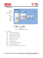
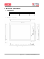
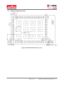
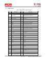
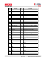
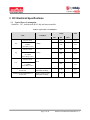
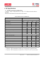
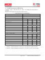
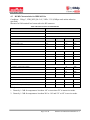
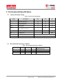
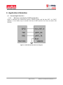
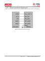
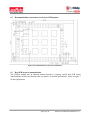
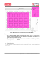
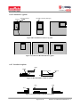
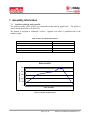
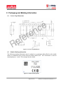
SN8200
Wi-Fi Network Controller Module
User Manual
And Datasheet
Version: 1.2
May 30, 2013
Note: SyChip, LLC. reserves the right to make changes in specifications at any time and without notice. The
information furnished in this data sheet is believed to be accurate and reliable. However, no responsibility is assumed
by SyChip for its use, nor any infringements of patents or other rights of third parties resulting from its use. No license
is generated under any rights of SyChip or its supporters unless specifically agreed.
Revision History
Revision
Date
Author
Change Description
0.1
12/09/2012
Y. Fang
Initial version
0.5
02/03/2012
Y. Fang
Preliminary version
0.6
2/20/2012
N. Nagayama
0.7
04/20/2012
J. Gregus
1.0
08/27/2012
Y. Fang
Formal Release
1.1
01/23/2013
Y. Fang
Added Power Rail Current Specification and Standby
Mode Current Consumption
1.2
05/30/2013
R. Willett
Changed specs in Table 1 for Pin 2, 3, 4, and 30
Update performance data and adjusted table format
Update CE compliance information
Page 2 of 30
SN8200 User Manual and Datasheet v1.2
Table of Contents
1
SYSTEM DESCRIPTIONS ..................................................................................................................................... 6
1.1
1.2
1.3
1.4
2
MECHANICAL SPECIFICATIONS ..................................................................................................................... 8
2.1
2.2
2.3
2.4
3
DC/RF CHARACTERISTICS FOR IEEE 802.11B ..................................................................................................... 14
DC/RF CHARACTERISTICS FOR IEEE 802.11G ..................................................................................................... 15
DC/RF CHARACTERISTICS FOR IEEE 802.11N ..................................................................................................... 16
ENVIRONMENTAL SPECIFICATIONS ........................................................................................................... 17
5.1
5.2
6
TYPICAL POWER CONSUMPTION........................................................................................................................... 13
RF SPECIFICATIONS .......................................................................................................................................... 14
4.1
4.2
4.3
5
MODULE DIMENSION .............................................................................................................................................. 8
MODULE TOP AND SIDE VIEW ................................................................................................................................. 8
MODULE FOOTPRINT (TOP VIEW) ............................................................................................................................ 9
MODULE PIN-OUT................................................................................................................................................. 10
DC ELECTRICAL SPECIFICATIONS .............................................................................................................. 13
3.1
4
APPLICATIONS ........................................................................................................................................................ 6
MODULE SUMMARY ............................................................................................................................................... 6
BLOCK DIAGRAM ................................................................................................................................................... 7
ACRONYMS............................................................................................................................................................. 7
ABSOLUTE MAXIMUM RATINGS ............................................................................................................................ 17
RECOMMENDED OPERATING CONDITIONS ............................................................................................................ 17
APPLICATION INFORMATION........................................................................................................................ 18
6.1 EXTERNAL DIGITAL INTERFACES .......................................................................................................................... 18
6.1.1
Reference connection for UART host interface .......................................................................................... 18
6.1.2
Reference connection for the SPI host interface ........................................................................................ 19
6.2 RECOMMENDED HOST (CUSTOMER) CIRCUIT BOARD PCB PATTERN ..................................................................... 20
6.3 HOST PCB LAYOUT RECOMMENDATIONS ............................................................................................................. 20
6.4 MODULE LOCATION ............................................................................................................................................. 21
6.4.1
Location in x-y plane .................................................................................................................................. 22
6.4.2
Location in z-plane ..................................................................................................................................... 22
7
ASSEMBLY INFORMATION ............................................................................................................................. 23
7.1
8
LEAD-FREE SOLDERING REFLOW PROFILE ............................................................................................................. 23
PACKAGING AND MARKING INFORMATION ............................................................................................ 24
8.1
8.2
CARRIER TAPE DIMENSIONS ................................................................................................................................. 24
MODULE MARKING INFORMATION ....................................................................................................................... 24
9
ORDERING INFORMATION ............................................................................................................................. 25
10
ROHS DECLARATION ........................................................................................................................................ 25
11
REGULATORY INFORMATION ....................................................................................................................... 25
11.1
11.2
11.3
11.4
11.5
11.6
FCC NOTICE (USA) ........................................................................................................................................ 25
FCC LABELING REQUIREMENTS ...................................................................................................................... 26
RF EXPOSURE .................................................................................................................................................. 26
IC NOTICE (CANADA) ...................................................................................................................................... 26
IC LABELING REQUIREMENTS ......................................................................................................................... 27
CE NOTICE (EUROPE) ...................................................................................................................................... 27
Page 3 of 30
SN8200 User Manual and Datasheet v1.2
11.7
CE LABELING REQUIREMENTS ........................................................................................................................ 27
12
TECHNICAL SUPPORT CONTACT ................................................................................................................. 28
13
DISCLAIMER ........................................................................................................................................................ 28
Page 4 of 30
SN8200 User Manual and Datasheet v1.2
LIST OF FIGURES
FIGURE 1 SN8200 MODULE BLOCK DIAGRAM ..................................................................................................................... 7
FIGURE 2 MODULE TOP AND SIDE VIEW .............................................................................................................................. 8
FIGURE 3 DETAILED MECHANICAL DATA (TOP VIEW) .......................................................................................................... 9
FIGURE 4 UART HOST INTERFACE REFERENCE DIAGRAM ................................................................................................. 18
FIGURE 5 SPI HOST INTERFACE REFERENCE DIAGRAM ...................................................................................................... 19
FIGURE 6 RECOMMENDED HOST (CUSTOMER) PCB PATTERN ............................................................................................ 20
FIGURE 7 RECOMMENDED HOST CIRCUIT BOARD DESIGN UNDERNEATH THE MODULE ..................................................... 21
FIGURE 8 RECOMMENDED LOCATIONS IN XY-PLANE .......................................................................................................... 22
FIGURE 9 LOCATIONS NOT RECOMMENDED IN XY-PLANE .................................................................................................. 22
FIGURE 10 RECOMMENDED LOCATIONS IN Z-PLANE ........................................................................................................... 22
FIGURE 11 LOCATIONS NOT RECOMMENDED IN XY-PLANE ................................................................................................ 22
FIGURE 12 REFLOW PROFILE PATTERN .............................................................................................................................. 23
FIGURE 13 CARRIER TAPE DIMENSIONS ............................................................................................................................. 24
FIGURE 14 MODULE MARKING DETAIL ............................................................................................................................. 24
LIST OF TABLES
TABLE 1 MODULE CONNECTOR SIGNAL DESCRIPTION ...................................................................................................... 10
TABLE 2 TYPICAL POWER CONSUMPTION .......................................................................................................................... 13
TABLE 3 RF CHARACTERISTICS FOR IEEE 802.11B ........................................................................................................... 14
TABLE 4 RF CHARACTERISTICS FOR IEEE 802.11G............................................................................................................ 15
TABLE 5 RF CHARACTERISTICS FOR IEEE 802.11N............................................................................................................ 16
TABLE 6 ABSOLUTE MAXIMUM RATING ............................................................................................................................ 17
TABLE 7 RECOMMENDED OPERATING CONDITIONS ........................................................................................................... 17
TABLE 8 REFLOW PROFILE RECOMMENDATION ................................................................................................................. 23
Page 5 of 30
SN8200 User Manual and Datasheet v1.2
1 System Descriptions
1.1 Applications
SN8200 is a complete low power self-contained embedded wireless solution to address the
connectivity demand in M2M applications. It integrates micro-controller, Wi-Fi BB/MAC/RF IC,
RF front end, clocks, and on-board antenna into a small form factor module. SN8200 can be
controlled by a host device through a serial interface; it can also serve as a standalone Wi-Fi
station or network controller. Thus, it can be used to enable wireless connectivity to the simplest
products with minimal engineering resources.
The SN8200 provides standard IEEE802.11 b/g/n functions. The integrated MCU supports
Broadcom WICED™ software. It can be used for a variety of different applications, such as
wireless sensor node, serial to Wi-Fi transceiver, Wi-Fi network controller, Wi-Fi gateway/bridges
plus internet server.
When used in a system where the SN8200 is controlled by a host CPU, the serial host interface
makes it very easy to integrate. When used in a system without a host CPU, the integrated ARM
Cortex-M3 can be used to run a variety of applications.
The SN8200 Wi-Fi module can be used for Wi-Fi gateway if combined with other radio module.
For example, one can design a Zigbee Wi-Fi gateway by combine SN8200 with SyChip SN3020
Zigbee module. SyChip provides a reference design to enable the OEM customer. This gateway
design can be used for low cost and low power consumption applications like Home Area
Networks.
1.2 Module Summary
• 2.4GHz IEEE 802.11b/g/n radio technology
• Dimension: 30.5 mm × 19.4 mm × 2.8 mm
• On-board antenna
• Transmit power: +18 dBm @ 11b /11Mbps
• Max receive sensitivity: -96dBm
• MCU: ARM Cortex-M3
• Diverse serial interface: UART, SPI
• Sensor applications support: ADC, DAC, I2C, GPIO
• Operating temperature range: -30ºC to 85ºC
• RoHS compliant
• MSL Level 3
• FCC/IC certified; CE compliant
Page 6 of 30
SN8200 User Manual and Datasheet v1.2
1.3
Block Diagram
Figure 1 SN8200 Module Block Diagram
1.4
Acronyms
ADC Analog to Digital Converter
GPIO
General-Purpose Input-Output
I2C
Intelligent Interface Controller
ISM
Industrial, Scientific and Medical
MAC
Medium Access Control
MSL
Moisture Sensitivity Level
PER
Packet Error Rate
ROHS Restriction of Hazardous Substances
SPI
Serial Peripheral Interface
UART Universal Asynchronous Receiver-Transmitter
Page 7 of 30
SN8200 User Manual and Datasheet v1.2
2 Mechanical Specifications
2.1
2.2
Module dimension
Parameter
Typical
Units
Dimension (LxWxH)
Dimension tolerances (LxWxH)
30.5 x 19.4 x 2.8
±0.2
mm
mm
Module top and side view
Figure 2 Module Top and Side View
Page 8 of 30
SN8200 User Manual and Datasheet v1.2
2.3
Module footprint (top view)
Figure 3 Detailed Mechanical Data (top view)
Page 9 of 30
SN8200 User Manual and Datasheet v1.2
2.4
Module Pin-out
Table 1 Module Connector Signal Description
Pin #
1
2
Pin name
GND
OSC32_IN
I/O
-
Description
Ground
I/O
Optional precision 32.768 kHz slow clock
input. No connect if not used
3
OSC32_OUT
I/O
No connect
4
WIFI_VDD_EN
I/O
No connect
5
ADC3
I/O
General purpose I/O or ADC3
6
ADC4
I/O
General purpose I/O or ADC4
7
ADC5
I/O
General purpose I/O or ADC5
8
VDD
PI
DC supply for MCU and I/O
9
ADC6
I/O
General purpose I/O or ADC6
10
DAC2
I/O
General purpose I/O or DAC2
11
DAC1
I/O
General purpose I/O or DAC1
12
ADC1
I/O
General purpose I/O or ADC1
13
Reserved
-
No connect
14
Reserved
-
No connect
15
GND
-
Ground
16
GND
-
Ground
17
GND
-
Ground
18
GND
-
Ground
19
GND
-
Ground
20
GND
-
Ground
21
GND
-
Ground
22
GND
-
Ground
23
GND
-
Ground
24
GND
-
Ground
25
GND
-
Ground
26
VDD_WIFI_IN
PI
Wi-Fi power supply
27
Reserved
-
No connect
28
Reserved
-
No connect
29
Reserved
-
No connect
30
WIFI_SLEEP_CLK_IN
I
Optional precision 32.768 kHz Wi-Fi sleep
Page 10 of 30
SN8200 User Manual and Datasheet v1.2
Pin #
Pin name
I/O
Description
clock input. Tie to GND if not used
31
GND
32
UART_TX
I/O
General purpose I/O or UART_TX
33
UART_RX
I/O
General purpose I/O or UART_RX
34
UART_CTS
I/O
General purpose I/O or UART_CTS
35
UART_RTS
I/O
General purpose I/O or UART_RTS
36
JTMS
I/O
General purpose I/O or JTMS
37
JTDI/SPI_NSS
I/O
General purpose I/O or JTDI or SPI_NSS
38
JTCK
I/O
General purpose I/O or JTCK
39
Ground
40
JTDO/SPI_SCK
I/O
General purpose I/O or JTDO or SPI_SCK
41
JTRST/SPI_MISO
I/O
General purpose I/O or JTRST or SPI_MISO
42
SPI_MOSI
I/O
General purpose I/O or SPI_MOSI
43
I2C_SCL
I/O
General purpose I/O or I2C_SCL
44
I2C_SDA
I/O
General purpose I/O or I2C_SDA
45
-
BOOT
46
ADC2
47
MICRO_RST_N
48
-
VBAT
I/O
Ground
Ground
Normal operation if connected to ground at
power up.
General purpose I/O or ADC2
I
Module reset
PI
Power supply for backup circuitry when
VDD is not present
49
GND
-
Ground
50
GND
-
Ground
51
GND
-
Ground
52
GND
-
Ground
53
GND
-
Ground
54
GND
-
Ground
55
GND
-
Ground
56
GND
-
Ground
57
GND
-
Ground
58
GND
-
Ground
59
GND
-
Ground
60
GND
-
Ground
Page 11 of 30
SN8200 User Manual and Datasheet v1.2
Pin #
Pin name
I/O
Description
61
Reserved
-
No connect
62
GND
-
Ground
Page 12 of 30
SN8200 User Manual and Datasheet v1.2
3 DC Electrical Specifications
3.1 Typical Power Consumption
Condition: 25C, includes both Wi-Fi chip and microcontroller
Table 2 Typical Power Consumption
Values
Item
Min
Receive mode
11b
Transmit mode
(18dBm/
100% Duty Cycle)
11Mbps
Receive mode
11g
Transmit mode
(14.5 dBm/
100 % Duty Cycle)
Transmit mode
(13.5dBm/
100% Duty Cycle)
Typ
Max
110
mA
370
mA
110
mA
290
mA
110
mA
280
mA
54Mbps
Receive mode
11n
Units
Condition
MCS7
Standby Mode with IEEE802.11
Power Save
DTIM 1, Telnet session
established and idling
3.15
mA
Standby Mode with IEEE802.11
Power Save
DTIM 3, Telnet session
established and idling
1.28
mA
Page 13 of 30
SN8200 User Manual and Datasheet v1.2
4 RF Specifications
4.1 DC/RF Characteristics for IEEE 802.11b
Conditions: 25deg.C, VDD_WIFI_IN=3.6V, VDD= 3.3V (11Mbps mode unless otherwise
specified.)
Measured at 50Ω terminal load connected to the RF connector
Table 3 RF Characteristics for IEEE 802.11b
Parameters
Specification
Modulation
DSSS/CCK
Physical layer data rate
1,2,5.5,11Mbps
RF Characteristics
Min
Typ.
Max.
Unit
Frequency range
2400
--
2483.5
MHz
Carrier frequency error
-20
--
+20
ppm
Transmit output power
16
18
20
dBm
--
--
-30
dBr
--
--
-50
dBr
Power-on and Power-down ramp
--
--
2
usec
RF Carrier Suppression
15
--
--
dBc
Modulation accuracy (EVM)
--
--
35
%
30MHz to 1GHz (BW=100KHz)
-96
dBm
1GHz to 12.75GHz (BW=1MHz)
-41
dBm
1.8GHz to 1.9GHz (BW=1MHz)
-65
dBm
5.15GHz to5.3GHz (BW=1MHz)
-85
dBm
Spectrum mask
1st side lobes
nd
2 side lobes
Outband spurious emissions
Receive Minimum Sensitivity
1Mbps (FER≤ 8%)
-94
-96
--
dBm
11Mbps (FER≤ 8%)
-86
-88
--
dBm
Maximum input level (FER≤ 8%)
-9.5
--
--
dBm
Adjacent channel rejection (FER≤ 8%)
35
dB
[Note]
1. Derate by 1.5 dB for temperatures less than -10C or more than 55C in transceiver mode.
2. Derate by 1.5 dB for temperatures less than-30C to -10C and 55C to 85C in receiver mode.
Page 14 of 30
SN8200 User Manual and Datasheet v1.2
4.2 DC/RF Characteristics for IEEE 802.11g
Conditions: 25deg.C, VDD_WIFI_IN=3.6V, VDD= 3.3V (54Mbps mode unless otherwise
specified.)
Measured at 50Ω terminal load connected to the RF connector
Table 4 RF Characteristics for IEEE 802.11g
Parameters
Specification
Standard conformance
IEEE 802.11 g
Modulation
OFDM
Data rate
6, 9, 12, 18, 24, 36, 48, 54Mbps
RF Characteristics
Min
Typ.
Max.
Unit
Frequency range
2400
--
2483.5
MHz
Carrier frequency error
-20
--
+20
ppm
Transmit output power
12.5
14.5
16.5
dBm
Spectrum mask
9MHz to 11MHz (0dB ~ -20dB)
0
-
dB
11MHz to 20MHz (-20dB ~ -28dB)
0
-
dB
20MHz to 30MHz (-28dB ~ -40dB)
0
-
dB
30MHz to 33MHz (-40dB)
0
-
dB
-25
dB
30MHz to 1GHz (BW=100KHz)
-96
dBm
1GHz to 12.75GHz (BW=1MHz)
-41
dBm
1.8GHz to 1.9GHz (BW=1MHz)
-65
dBm
5.15GHz to5.3GHz (BW=1MHz)
-85
dBm
Constellation Error (EVM)
--
--
Outband spurious emissions
Received Minimum Sensitivity
6Mbps (PER≤ 10%)
-87
-89
--
dBm
54Mbps (PER ≤ 10%)
-72
-74
--
dBm
Maximum input level (PER ≤ 10%)
-13
--
--
dBm
Adjacent channel rejection (PER ≤ 10%)
-1
dB
[Note]
1. Derate by 1.5 dB for temperatures less than -10C or more than 55C in transceiver mode.
2. Derate by 1.5 dB for temperatures less than-30C to -10C and 55C to 85C in receiver mode.
Page 15 of 30
SN8200 User Manual and Datasheet v1.2
4.3 DC/RF Characteristics for IEEE 802.11n
Conditions: 25deg.C, VDD_WIFI_IN=3.6V, VDD= 3.3V (65Mbps mode unless otherwise
specified.)
Measured at 50Ω terminal load connected to the RF connector
Table 5 RF Characteristics for IEEE 802.11n
Parameters
Specification
Standard conformance
IEEE 802.11 n
Modulation
OFDM
Data rate
6.5, 13, 19.5, 26, 39, 52, 58.5, 65Mbps
RF Characteristics
Min
Typ.
Max.
Unit
Frequency range
2400
--
2483.5
MHz
Carrier frequency error
-20
--
+20
Ppm
Power level
11
13
15
dBm
Spectrum mask
9MHz to 11MHz (0dB ~ -20dB)
0
-
dB
11MHz to 20MHz (-20dB ~ -28dB)
0
-
dB
20MHz to 30MHz (-28dB ~ -45dB)
0
-
dB
30MHz to 33MHz (-45dB)
0
-
dB
-28
dB
30MHz to 1GHz (BW=100KHz)
-96
dBm
1GHz to 12.75GHz (BW=1MHz)
-41
dBm
1.8GHz to 1.9GHz (BW=1MHz)
-65
dBm
5.15GHz to5.3GHz (BW=1MHz)
-85
dBm
--
dBm
Constellation Error (EVM)
--
--
Outband spurious emissions
Received Minimum Sensitivity
65Mbps (PER ≤ 10%)
-69
-71
Maximum input level (PER ≤ 10%)
-13
dB
Adjacent channel rejection (PER ≤ 10%)
-2
dB
[Note]
1. Derate by 1.5 dB for temperatures less than -10C or more than 55C in transceiver mode.
2. Derate by 1.5 dB for temperatures less than-30C to -10C and 55C to 85C in receiver mode.
Page 16 of 30
SN8200 User Manual and Datasheet v1.2
5 Environmental Specifications
5.1
Absolute maximum ratings
Table 6 Absolute Maximum Rating
Symbol
5.2
Description
Min
Max
Unit
Top
Operating temperature
-30
85
°C
Tst
Storage temperature
-40
85
°C
VDD
Power supply
0
4.0
V
VBAT
Power supply for backup circuitry
when VDD is not present
0
4.0
V
VDD_WiFi
Wi-Fi Power supply
0
6.0
V
RFin
RF input power
0
dBm
MSL
Moisture Sensitivity Level
RoHS
Restriction of Hazardous Substances
3
Compliant
Recommended Operating Conditions
Table 7 Recommended Operating Conditions
VDD
VBAT
VDD_WiFi
Min (V)
Typical (V)
Max (V)
2.4
2.0
3.4
3.3
3.3
3.6
3.6
3.6
4.0
Page 17 of 30
Supply Current
Specification (mA)
150
10
500
SN8200 User Manual and Datasheet v1.2
6 Application Information
6.1
External digital interfaces
6.1.1
Reference connection for UART host interface
Figure 4 illustrates the connections between SN8200 module and the host MCU via UART
interface. A level shifter may be needed if the host UART interface level does not match with
SN8200.
Figure 4 UART Host Interface Reference Diagram
Page 18 of 30
SN8200 User Manual and Datasheet v1.2
6.1.2
Reference connection for the SPI host interface
Figure 5 illustrates the connections between SN8200 module and the host MCU via SPI interface.
Figure 5 SPI Host Interface Reference Diagram
Page 19 of 30
SN8200 User Manual and Datasheet v1.2
6.2
Recommended host (customer) circuit board PCB pattern
Figure 6 Recommended Host (customer) PCB Pattern
6.3 Host PCB layout recommendations
The SN8200 module has an onboard antenna therefore it requires careful host PCB layout
underneath the module such that the radio can achieve its best RF performance. Refer to Figure 7
for the requirements.
Page 20 of 30
SN8200 User Manual and Datasheet v1.2
Figure 7 Recommended Host Circuit Board Design underneath the Module
Notes:
1. Due to the surface mount antenna on the module, the area in ‘Zone1’ on all layers of the
customer circuit board should be free of any metal objects. Specifically, there should be no
ground plane, traces or metal shield case.
2. The area in ‘Zone2’ on the top layer of the customer circuit board should have ground only
with no signal traces.
6.4 Module Location
For optimum EIRP, customer is advised to use the recommended module location on their host
circuit board.
Page 21 of 30
SN8200 User Manual and Datasheet v1.2
6.4.1 Location in x-y plane
Antenna Connector
No GND in this area (See Fig.8)
Antenna
Shield Case
Figure 8 Recommended Locations in xy-plane
Figure 9 Locations Not Recommended in xy-plane
6.4.2 Location in z-plane
Metal
Module
Antenna Connector
Antenna
Mother Board
Metal
Figure 10 Recommended Locations in z-plane
Metal
Metal
Metal
Figure 11 Locations Not Recommended in xy-plane
Page 22 of 30
SN8200 User Manual and Datasheet v1.2
7 Assembly Information
7.1 Lead-free soldering reflow profile
The lead-free solder reflow profile is recommended in the table & graph below. The profile is
used to attach the module to its host PCB.
The module is designed to withstand 2 reflows. Opposite side reflow is prohibited due to the
module weight.
Table 8 Reflow Profile Recommendation
Ramp up rate
Maximum time maintained above 217oC
Peak temperature
Maximum time within 5oC of peak temperature
Ramp down rate
3oC/second max
120 seconds
250oC
20 seconds
6oC/second max
Reflow Profile
Temperature, C
250
200
150
100
50
0
Time, seconds
Figure 12 Reflow Profile Pattern
Page 23 of 30
SN8200 User Manual and Datasheet v1.2
8 Packaging and Marking Information
8.1
Carrier Tape Dimensions
Figure 13 Carrier Tape Dimensions
8.2 Module Marking Information
The following marking information may be printed on a permanent label affixed to the module
shield or permanently laser written into the module shield itself. The 2D barcode is used for
internal purposes. A pin 1 ID is stamped into the shield.
Figure 14 Module Marking Detail
Page 24 of 30
SN8200 User Manual and Datasheet v1.2
9 Ordering Information
Table 9 Ordering Information
SyChip Model
Number
SyChip Part
Number
Standard Order
Increment
*Evaluation Development Kit
SN8200EVK
88-00151-85
1 pc
Evaluation Development Kit+
SN8200EVK+
88-00151-95
1 pc
SN8200
88-00151-00
400 pcs
Product
Module in Tape & Reel
10 RoHS Declaration
To the best of our present knowledge, given our supplier declarations, this product does not contain
substances that are banned by Directive 2002/95/EC or contain a maximum concentration of 0.1%
by weight in homogeneous materials for
• Lead and lead compounds
• Mercury and mercury compounds
• Chromium (VI)
• PBB (polybrominated biphenyl)
• PBDE (polybrominated biphenyl ether)
And a maximum concentration of 0.01% by weight in homogeneous materials for
• Cadmium and cadmium compounds
11 Regulatory Information
SN8200 has obtained the certifications described below.
11.1 FCC Notice (USA)
This device complies with Part 15 of the FCC rules. Operation is subject to the following two
conditions: (1) this device may not cause harmful interference, and (2) this device must accept any
interference received, including interference that may cause undesired operation.
The FCC requires the OEM to be notified that any changes or modifications not expressly approved
by SyChip, LLC may void the user’s authority to operate the equipment. While an application of the
SN8200 module in a product is not required to obtain a new FCC authorization for the module, this
does not preclude the possibility that some other form of authorization or testing may be required for
that end product.
This device using the integrated antenna has been tested to comply with FCC CFR Part 15. The
device meets the requirements for modular transmitter approval as detailed in the FCC public notice
DA00.1407.
Page 25 of 30
SN8200 User Manual and Datasheet v1.2
This equipment has been tested and found to comply with the limits for a Class B digital device,
pursuant to Part 15 of the FCC Rules. These limits are designed to provide reasonable protection
against harmful interference in a residential installation. This equipment generates uses and can
radiate radio frequency energy and, if not installed and used in accordance with the instructions, may
cause harmful interference to radio communications. However, there is no guarantee that
interference will not occur in a particular installation. If this equipment does cause harmful
interference to radio or television reception, which can be determined by turning the equipment off
and on, the user is encouraged to try to correct the interference by one or more of the following
measures: reorient or relocate the receiving antenna, increase the separation between the equipment
and receiver, connect the equipment into an outlet on a circuit different from that to which the
receiver is connected, or consult the dealer or an experienced radio/TV technician for help.
11.2 FCC Labeling Requirements
When integrating the SN8200 into a product the FCC labeling requirements must be met. This
includes a clearly visible label on the outside of the finished product specifying the SN8200 FCC
identifier (FCC ID:QPU8200) as well as the notice above. The exterior label can use wording such
as “Contains Transmitter Module FCC ID:QPU8200” or “Contains FCC ID:QPU8200” although
any similar wording that expresses the same meaning may be used.
11.3 RF Exposure
This module has been certified for remote and base radio applications and is not intended to be
operated within 20cm of the body. If the module will be used for portable applications, the device
must undergo SAR testing.
The following statement must be included as a CAUTION statement in manuals for the products to
alert users on FCC RF exposure compliance:
“WARNING: To satisfy FCC RF exposure requirements for mobile transmitting devices, a
separation distance of 20cm or more should be maintained between the antenna of this device and
persons during operation. To ensure compliance, operations at closer distances than this are not
recommended.”
11.4 IC Notice (Canada)
The term “IC” before the certification/registration number only signifies that the Industry Canada
technical specifications were met.
Le terme “IC” devant le numéro de certification /d’enregistrement signifie seulement que les
spécifications techniques Industrie Canada ont été respectées.
This device complies with Industry Canada license-exempt RSS standard(s). Operation is subject to
The following two conditions: (1) this device may not cause interference, and (2) this device must
accept any interference, including interference that may cause undesired operation of the device.
Page 26 of 30
SN8200 User Manual and Datasheet v1.2
Cet appareil est conforme avec Industrie Canada RSS standard exempts de licence (s). Son
utilisation est soumise à Les deux conditions suivantes: (1) cet appareil ne peut pas provoquer
d'interférences et (2) cet appareil doit accepter Toute interférence, y compris les interférences qui
peuvent causer un mauvais fonctionnement du dispositif.
This device complies with Health Canada’s Safety Code 6 / IC RSS-210. The installer of this device
should ensure that RF radiation is not emitted in excess of the Health Canada’s requirement.
Information can be obtained at: http://www.hc-sc.gc.ca/ewh-semt/pubs/radiation/radio_guidelignes_direct-eng.php
Cet appareil est conforme avec Santé Canada Code de sécurité 6 / IC RSS-210. Le programme
d'installation de cet appareil doit s'assurer que les rayonnements RF n'est pas émis au-delà de
l'exigence de Santé Canada. Les informations peuvent être obtenues: http://www.hc-sc.gc.ca/ewhsemt/pubs/radiation/radio_guide-lignes_direct-eng.php
11.5 IC Labeling Requirements
The host device should be properly labeled to identify the module within the host device. The
Industry Canada certification label of a module shall be clearly visible at all times when installed in
the host device, otherwise the host device must be labeled to display the Industry Canada
certification number of the module, preceded by the words “Contains transmitter module”, or the
word “Contains”, or similar wording expressing the same meaning, as follows:
Contains transmitter module IC:4523A-SN8200,
where 4523A-SN8200 is the module’s certification number.
11.6 CE Notice (Europe)
This device has been tested and certified for use in the European Union.
If this device is used in a product, the OEM has responsibility to verify compliance of the final
product to the EU standards. A Declaration of Conformity must be issued and kept on file as
described in Annex II of the Radio and Telecommunications Terminal Equipment Directive.
11.7 CE Labeling Requirements
The ‘CE’ mark must be placed on the OEM product per the labeling requirements of the Directive.
Given that the operating frequency band is not harmonized by a few European countries, the
restriction or alert sign must be placed alongside the ‘CE’ mark as shown below. As of the date of
this document, only France has a restriction. The restriction is that, if the radio is operated outdoors
in the 2450-2483.5 MHz band, the power must be limited to 10 mW instead of 100 mW. The OEM
must account for this and the product must have the alert mark. It does not require country
notifications, however.
Page 27 of 30
SN8200 User Manual and Datasheet v1.2
12 Technical Support Contact
SyChip LLC
2805 Dallas Parkway, Suite 400
Plano, TX 75093
USA
Tel: (972) 202-8900
Fax: (972) 633-0327
Note: SyChip LLC is an operating unit within Murata Wireless Solutions
13 Disclaimer
Please read this notice before using the SN8200 product.
1.
Please note that the only warranty that SyChip LLC (“SyChip”) provides regarding the
products is its conformance to the specifications provided herein. Accordingly, SyChip shall not be
responsible for any defects in products or equipment incorporating such products, which are caused
under the conditions other than those specified in this specification.
SYCHIP HEREBY DISCLAIMS ALL OTHER WARRANTIES REGARDING THE PRODUCTS,
EXPRESS OR IMPLIED, INCLUDING WITHOUT LIMITATION ANY WARRANTY OF
FITNESS FOR A PARTICULAR PURPOSE, THAT THEY ARE DEFECT-FREE, OR AGAINST
INFRINGEMENT OF INTELLECTUAL PROPERTY RIGHTS. YOU AGREE TO INDEMNIFY
AND DEFEND SYCHIP AND ITS AFFILIATES AGAINST ALL CLAIMS, DAMAGES, COSTS
AND EXPENSES THAT MAY BE INCURRED, INCLUDING WITHOUT LIMITATION,
ATTORNEY FEES AND COSTS, DUE TO THE USE OF PRODUCTS.
2.
The product is designed and manufactured for general applications, and not for any particular
application, so testing and use of the product shall be conducted at your own risk and responsibility.
Specifically, please observe the following:
i) Please conduct validation and verification of the products in actual condition of
mounting and operating environment before commercial shipment of the
equipment.
ii) Please pay attention to minimize any mechanical vibration or shock, not to drop
the product or a substrate that contains the product during transportation.
iii) Since the application of static electricity or overvoltage may cause a defect in the
product or deterioration of its reliability, caution must be taken against exposure
to any static electricity generated by electrified items such as work benches,
soldering irons, tools, carrying containers, etc.
iv) Caution shall be taken to avoid overstress to the product during and after the
soldering process.
Page 28 of 30
SN8200 User Manual and Datasheet v1.2
v) Since the applied soldering method may deteriorate the reliability, thorough
evaluation is recommended.
vi) In case the product is to be used in equipment or electric circuit that requires high
safety or reliability function or performance, sufficient reliability evaluation
checks for safety shall be performed before commercial shipment and moreover,
due consideration to install a protective circuit is strongly recommended at
customer's design stage. Please provide an appropriate fail-safe function on your
product to prevent any damages that may be caused by the abnormal function or
the failure of our product.
Notwithstanding the foregoing, the product shall not be used in any application listed below which
requires especially high reliability for the prevention of such defect as may directly cause damage to
the third party's life, body or property.
- Aircraft equipment
- Aerospace equipment
- Undersea equipment
- Power plant control equipment
- Medical equipment
- Transportation equipment (vehicles, trains, ships, etc.)
- Traffic signal equipment
- Disaster prevention / crime prevention equipment
- Application of similar complexity and/or reliability requirements to the applications listed in the
above.
3.
SyChip’s warranty as provided in Clause 1 above that the products comply with descriptions
expressly specified in the specifications shall be effective for a period of six (6) months from the
date of delivery. SyChip shall not be liable for any defects that occur in dry packed products that are
installed more than six (6) months after shipment.
SyChip’s liability under this warranty shall be limited to products that are returned during the
warranty period to the address designated by SyChip and that are determined by SyChip not to
conform to such warranty. If SyChip elects to repair or replace such products, SyChip shall have
reasonable time to repair such products or provide replacements. Repaired products shall be
warranted for the remainder of the original warranty period. Replaced products shall be warranted
for a new full warranty period.
For avoidance of doubt, SyChip shall not be liable for any defects that are caused by neglect, misuse
or mistreatment by an entity other than SyChip including improper installation or testing, or for any
products that have been altered or modified in any way by an entity other than SyChip. Moreover,
SyChip shall not be liable for any defects that result from your or third party’s design, specifications
or instructions for such products.
Page 29 of 30
SN8200 User Manual and Datasheet v1.2
4.
Testing and other quality control techniques are used to the extent SyChip deems necessary.
Unless mandated by government requirements, SyChip does not necessarily test all parameters of
each product.
5.
End of Life - Please note that we may discontinue the manufacture of products, due to
reasons such as, but not limited to, end of supply of materials and/or components from our suppliers.
Page 30 of 30
SN8200 User Manual and Datasheet v1.2
Mouser Electronics
Authorized Distributor
Click to View Pricing, Inventory, Delivery & Lifecycle Information:
Murata:
88-00151-85